KR102342804B1 - Organic light emitting display device - Google Patents
Organic light emitting display deviceDownload PDFInfo
- Publication number
- KR102342804B1 KR102342804B1KR1020140193876AKR20140193876AKR102342804B1KR 102342804 B1KR102342804 B1KR 102342804B1KR 1020140193876 AKR1020140193876 AKR 1020140193876AKR 20140193876 AKR20140193876 AKR 20140193876AKR 102342804 B1KR102342804 B1KR 102342804B1
- Authority
- KR
- South Korea
- Prior art keywords
- layer
- disposed
- light emitting
- organic light
- region
- Prior art date
- Legal status (The legal status is an assumption and is not a legal conclusion. Google has not performed a legal analysis and makes no representation as to the accuracy of the status listed.)
- Active
Links
Images


Classifications
- H—ELECTRICITY
- H10—SEMICONDUCTOR DEVICES; ELECTRIC SOLID-STATE DEVICES NOT OTHERWISE PROVIDED FOR
- H10K—ORGANIC ELECTRIC SOLID-STATE DEVICES
- H10K59/00—Integrated devices, or assemblies of multiple devices, comprising at least one organic light-emitting element covered by group H10K50/00
- H—ELECTRICITY
- H10—SEMICONDUCTOR DEVICES; ELECTRIC SOLID-STATE DEVICES NOT OTHERWISE PROVIDED FOR
- H10K—ORGANIC ELECTRIC SOLID-STATE DEVICES
- H10K59/00—Integrated devices, or assemblies of multiple devices, comprising at least one organic light-emitting element covered by group H10K50/00
- H10K59/80—Constructional details
- H10K59/84—Parallel electrical configurations of multiple OLEDs
- H—ELECTRICITY
- H10—SEMICONDUCTOR DEVICES; ELECTRIC SOLID-STATE DEVICES NOT OTHERWISE PROVIDED FOR
- H10K—ORGANIC ELECTRIC SOLID-STATE DEVICES
- H10K59/00—Integrated devices, or assemblies of multiple devices, comprising at least one organic light-emitting element covered by group H10K50/00
- H10K59/80—Constructional details
- H10K59/86—Series electrical configurations of multiple OLEDs
Landscapes
- Electroluminescent Light Sources (AREA)
- Devices For Indicating Variable Information By Combining Individual Elements (AREA)
Abstract
Translated fromKorean
Description
Translated fromKorean본 발명은 유기 발광 표시 장치에 관한 것으로서, 보다 상세하게는 표시 패널의 GIP 회로 내부의 산화물 반도체를 사용하는 TFT의 문턱 전압 변동이 최소화된 유기 발광 표시 장치에 관한 것이다.BACKGROUND OF THE
유기 발광 표시 장치는 자체 발광형 표시 장치로서, 액정 표시 장치와는 달리 별도의 광원이 필요하지 않아 경량 박형으로 제조 가능하다. 또한, 유기 발광 표시 장치는 저전압 구동에 의해 소비 전력 측면에서 유리할 뿐만 아니라, 색상 구현, 응답 속도, 시야각, 명암 대비비(contrast ratio; CR)도 우수하여, 차세대 디스플레이로서 연구되고 있다.The organic light emitting display device is a self-emission type display device, and unlike a liquid crystal display device, it does not require a separate light source, so it can be manufactured in a lightweight and thin form. In addition, the organic light emitting diode display is being studied as a next-generation display because it is advantageous in terms of power consumption due to low voltage driving, and has excellent color realization, response speed, viewing angle, and contrast ratio (CR).
유기 발광 표시 장치의 표시 패널은 스캔 라인과 데이터 라인들에 의해 구획되는 다수의 화소를 포함한다. 다수의 화소 각각은 유기 발광 소자 및 유기 발광 소자와 연결되어 이를 구동하는 화소 구동 회로를 포함한다. 화소 구동 회로는 스캔 라인의 게이트 펄스에 응답하여 데이터 전압을 구동 TFT의 게이트 전극에 공급하는 스캔 TFT 및 게이트 전극에 공급되는 데이터 전압에 따라 유기 발광 소자에 공급되는 전류의 양을 조절하는 구동 TFT와 데이터 전압을 소정 시간 저장하는 커패시터를 포함한다.A display panel of an organic light emitting diode display includes a plurality of pixels that are partitioned by scan lines and data lines. Each of the plurality of pixels includes an organic light emitting device and a pixel driving circuit connected to and driving the organic light emitting device. The pixel driving circuit includes a scan TFT that supplies a data voltage to the gate electrode of the driving TFT in response to a gate pulse of the scan line, and a driving TFT that adjusts the amount of current supplied to the organic light emitting diode according to the data voltage supplied to the gate electrode; and a capacitor for storing the data voltage for a predetermined time.
그리고 유기 발광 표시 장치는 스캔 라인과 데이터 라인들을 통해 각종의 신호를 이러한 각 화소의 화소 구동 회로에 공급하는, 데이터 드라이버와 게이트 드라이버를 포함한다.In addition, the organic light emitting diode display includes a data driver and a gate driver for supplying various signals to a pixel driving circuit of each pixel through scan lines and data lines.
보다 경량 박형화된, 유기 발광 표시 장치에 대한 시장의 요구에 따라, 베젤부를 최대한 얇게 제작하려는 시도가 이루어져 왔고, 이에 게이트 드라이버가 표시 패널 내부에 실장되는, GIP 방식(Gate Drive-IC in Panel)이 적용되고 있다. GIP 방식에 의하여 구성되는 GIP 회로는 TFT(TFT; Thin Film Transistor)는 액티브층으로 사용되는 물질에 따라 비정질 실리콘(amorphous-silicon)을 사용하는 TFT, 다결정 실리콘(poly-silicon)을 사용하는 TFT 또는 산화물 반도체를 사용하는 TFT 중 어느 하나를 포함할 수 있다. 그 중에서, 산화물 반도체를 사용하는 TFT의 경우 비정질 실리콘을 사용하는 TFT 대비하여 이동도가 우수하다. 또한, 비정질 실리콘이나 다결정 실리콘을 사용하는 TFT 대비하여 누설 전류(leakage current)가 현저히 낮다. 또한, 다결정 실리콘을 사용하는 TFT 대비하여 문턱 전압의 산포가 균일한 특성이 확보된다는 유리함이 있다.In response to the market demand for a lighter and thinner organic light emitting display device, attempts have been made to make the bezel part as thin as possible. Accordingly, a Gate Drive-IC in Panel (GIP) method in which a gate driver is mounted inside a display panel has been developed. is being applied In the GIP circuit constructed by the GIP method, TFT (Thin Film Transistor) is a TFT using amorphous-silicon, a TFT using poly-silicon, or a TFT using poly-silicon depending on the material used as the active layer. It may include any one of TFTs using an oxide semiconductor. Among them, in the case of a TFT using an oxide semiconductor, the mobility is excellent compared to a TFT using amorphous silicon. In addition, the leakage current is significantly lower than that of a TFT using amorphous silicon or polycrystalline silicon. In addition, there is an advantage in that a characteristic in which the distribution of the threshold voltage is uniform is secured compared to a TFT using polycrystalline silicon.
따라서, GIP 회로에 있어서 산화물 반도체를 사용하는 TFT를 유기 발광 표시 장치에 적용하기 위한 연구가 활발하게 진행되고 있다.Therefore, research for applying a TFT using an oxide semiconductor to an organic light emitting display device in a GIP circuit is being actively conducted.
그런데, 산화물 반도체는 소정한 캐리어 농도 구간에서, 캐리어 농도가 증가함에 따라 이동도가 증가하게 된다. 따라서 산화물 반도체의 캐리어 농도를 적절하게 조절하는 것이 산화물 반도체를 사용하는 TFT의 특성을 좌우한다. 이 때, 산화물 반도체에 산소의 빈격자점(Vacancy)이가 많이 존재할 수록, 산화물 반도체의 캐리어 농도가 증가된다. 또한, 산화물 반도체가 수소 등에 의하여 환원이 진행됨에 따라, 산화물 반도체 내의 캐리어 농도가 증가된다.However, the mobility of the oxide semiconductor increases as the carrier concentration increases in a predetermined carrier concentration section. Therefore, proper control of the carrier concentration of the oxide semiconductor influences the characteristics of the TFT using the oxide semiconductor. At this time, as the number of vacancies of oxygen in the oxide semiconductor increases, the carrier concentration of the oxide semiconductor increases. In addition, as the oxide semiconductor is reduced by hydrogen or the like, the carrier concentration in the oxide semiconductor increases.
산화물 반도체의 캐리어 농도가 증가됨에 따라 산화물 반도체를 사용하는 TFT의 문턱 전압이 음으로(Negative) 변동된다. 또한 산화물 반도체의 캐리어 농도가 소정의 농도를 넘어가게 되면, 산화물 반도체는 도체화 되어 반도체의 성질을 잃게 된다. 따라서, 산화물 반도체를 사용하는 TFT의 특성을 유지함에 있어서, 산화물 반도체의 캐리어 농도를 적절하게 조절하는 것은 매우 중요하다. 그런데, 산화물 반도체를 사용하는 TFT는, 유기 발광 표시 장치의 제조 공정 과정 및 장치의 사용 과정에서 외부로부터 여러가지 스트레스를 받게 됨에 따라 손상을 받을 수 있고 이로 인해 캐리어 농도가 변할 수 있다는 문제가 있다.As the carrier concentration of the oxide semiconductor increases, the threshold voltage of the TFT using the oxide semiconductor changes negatively. Also, when the carrier concentration of the oxide semiconductor exceeds a predetermined concentration, the oxide semiconductor becomes a conductor and loses properties of the semiconductor. Therefore, in maintaining the characteristics of the TFT using the oxide semiconductor, it is very important to properly control the carrier concentration of the oxide semiconductor. However, a TFT using an oxide semiconductor may be damaged as it is subjected to various external stresses during a manufacturing process of an organic light emitting display device and a process of using the device, thereby causing a problem in that a carrier concentration may change.
이에, 본 발명이 해결하고자 하는 과제는 합착층 경화를 위하여 가하는 고에너지의 영향으로부터 GIP 회로에 포함된 산화물 반도체를 사용한 TFT를 보호하는, 유기 발광 표시 장치를 제공하는 것이다.Accordingly, an object of the present invention is to provide an organic light emitting display device that protects a TFT using an oxide semiconductor included in a GIP circuit from the influence of high energy applied for curing the bonding layer.
이로써, 종국적으로는 산화물 반도체를 사용하는 TFT의 특성이 변동이 최소화되어 유기 발광 표시 장치의 성능이 보다 향상되는, 유기 발광 표시 장치를 제공하는 것이다.Accordingly, ultimately, an organic light emitting diode display device in which the characteristics of the TFT using the oxide semiconductor are minimized to further improve the performance of the organic light emitting display device is provided.
본 발명의 과제들은 이상에서 언급한 과제들로 제한되지 않으며, 언급되지 않은 또 다른 과제들은 아래의 기재로부터 당업자에게 명확하게 이해될 수 있을 것이다.The problems of the present invention are not limited to the problems mentioned above, and other problems not mentioned will be clearly understood by those skilled in the art from the following description.
본 발명의 실시예에 따른 유기 발광 표시 장치가 제공된다.An organic light emitting display device according to an embodiment of the present invention is provided.
본 발명의 실시예에 따른 유기 발광 표시 장치는 유기 발광 소자 및 화소 구동 회로를 포함하는 다수의 화소가 배치된 표시 영역과, 각각의 화소에 연결되는 GIP 회로가 배치된 비표시 영역이 정의된 하부 기판, 하부 기판과 서로 대향하고, 표시 영역에 대응하여 컬러 필터가 배치된 상부 기판 및, 하부 기판과 상부 기판 사이에 배치되고, 비표시 영역에 대응하여 배치된 제1 합착 영역 및 제1 합착 영역에 의하여 둘러싸이는 제2 합착 영역을 포함하는 합착층을 포함하고, 제2 합착 영역은, 비표시 영역에 대응하여, 제1 합착 영역과 제2 합착 영역이 직접 접촉하는 지점으로부터 표시 영역을 향하여 제1 폭을 가지는, 제2 합착 영역-노출영역을 가지고, 비표시 영역에 대응하여, GIP 회로와 합착층 사이에, 자외선을 반사하는 반사층이 배치되는 것을 특징으로 한다.In an organic light emitting diode display according to an embodiment of the present invention, a lower portion is defined in which a display area including a plurality of pixels including an organic light emitting element and a pixel driving circuit is disposed and a non-display area in which a GIP circuit connected to each pixel is disposed. The substrate, the upper substrate facing the lower substrate and having a color filter disposed to correspond to the display area, and the first junction region and the first junction region disposed between the lower substrate and the upper substrate and disposed to correspond to the non-display area and a closure layer including a second junction region surrounded by It has a second bonding area-exposed area having a width of one, and a reflective layer for reflecting ultraviolet rays is disposed between the GIP circuit and the bonding layer to correspond to the non-display area.
또한, 본 발명의 실시예에 따른 유기 발광 표시 장치에 있어서, 제1 합착 영역은 자외선에 의하여 경화된, 제1 합착 영역인 것을 특징으로 한다.In addition, in the organic light emitting diode display according to an embodiment of the present invention, the first bonding area is a first bonding area cured by ultraviolet light.
또한, 본 발명의 실시예에 따른 유기 발광 표시 장치에 있어서, 제1 합착 영역은 광중합체를 포함하는 것을 특징으로 한다.Also, in the organic light emitting diode display according to an embodiment of the present invention, the first bonding region may include a photopolymer.
또한, 본 발명의 실시예에 따른 유기 발광 표시 장치에 있어서, 제2 합착 영역은 자외선이 투과되는 것을 특징으로 한다.In addition, in the organic light emitting diode display according to an embodiment of the present invention, the second bonding region is characterized in that ultraviolet light is transmitted.
또한, 본 발명의 실시예에 따른 유기 발광 표시 장치에 있어서, 제2 합착 영역의 굴절률은 제1 합착 영역의 굴절률과 다른 것을 특징으로 한다.In addition, in the organic light emitting diode display according to an embodiment of the present invention, a refractive index of the second junction region is different from a refractive index of the first junction region.
또한, 본 발명의 실시예에 따른 유기 발광 표시 장치에 있어서, 반사층은 GIP 회로에 포함된 산화물 반도체를 사용하는 TFT를 모두 덮는 것을 특징으로 한다.In addition, in the organic light emitting diode display according to the embodiment of the present invention, the reflective layer is characterized in that it covers all TFTs using the oxide semiconductor included in the GIP circuit.
또한, 본 발명의 실시예에 따른 유기 발광 표시 장치에 있어서, GIP 회로는 다수의 산화물 반도체를 사용하는 TFT를 포함하는 것을 특징으로 한다.In addition, in the organic light emitting diode display according to the embodiment of the present invention, the GIP circuit is characterized in that it includes a TFT using a plurality of oxide semiconductors.
또한, 본 발명의 실시예에 따른 유기 발광 표시 장치에 있어서, 반사층은, 화소 구동 회로 및 GIP 회로 상에 배치된 제1 패시베이션층과, 제1 패시베이션층 상에 배치된 제1 오버 코팅층 사이에 배치된 제1 반사층인 것을 특징으로 한다.Further, in the organic light emitting diode display according to the embodiment of the present invention, the reflective layer is disposed between the first passivation layer disposed on the pixel driving circuit and the GIP circuit and the first overcoat layer disposed on the first passivation layer. It is characterized in that it is a first reflective layer.
또한, 본 발명의 실시예에 따른 유기 발광 표시 장치에 있어서, 제1 반사층을 구성하는 물질은 표시 영역에 대응하여, 제1 패시베이션층과 제1 오버 코팅층 사이에 배치된 제1 보조 전극을 구성하는 물질과 동일한 것을 특징으로 한다.In addition, in the organic light emitting diode display according to an embodiment of the present invention, the material constituting the first reflective layer corresponds to the display area and forms the first auxiliary electrode disposed between the first passivation layer and the first overcoat layer. Characterized by the same material.
또한, 본 발명의 실시예에 따른 유기 발광 표시 장치에 있어서, 제1 반사층의 두께는 표시 영역에 대응하여, 제1 패시베이션층과 제1 오버 코팅층 사이에 배치된 제1 보조 전극의 두께와 동일한 것을 특징으로 한다.In addition, in the organic light emitting diode display according to the embodiment of the present invention, the thickness of the first reflective layer is the same as the thickness of the first auxiliary electrode disposed between the first passivation layer and the first overcoat layer corresponding to the display area. characterized.
또한, 본 발명의 실시예에 따른 유기 발광 표시 장치에 있어서, 화소 구동 회로 및 GIP 회로 상에 순차로 배치된 제1 패시베이션층, 제1 오버 코팅층 및 뱅크를 더 포함하고, 반사층은 제1 오버 코팅층과 뱅크 사이에 배치된 제2 반사층인 것을 특징으로 한다.Further, in the organic light emitting diode display according to the embodiment of the present invention, the display device further includes a first passivation layer, a first overcoat layer, and a bank sequentially disposed on the pixel driving circuit and the GIP circuit, and the reflective layer is the first overcoating layer. and a second reflective layer disposed between the bank and the bank.
또한, 본 발명의 실시예에 따른 유기 발광 표시 장치에 있어서, 제2 반사층을 구성하는 물질은 제1 오버 코팅층 상에 배치된 유기 발광 소자에 포함된 화소 전극을 구성하는 물질과 동일한 것을 특징으로 한다.Further, in the organic light emitting diode display according to the embodiment of the present invention, the material constituting the second reflective layer is the same as the material constituting the pixel electrode included in the organic light emitting device disposed on the first overcoat layer. .
또한, 본 발명의 실시예에 따른 유기 발광 표시 장치에 있어서, 제2 반사층의 두께는 제1 오버 코팅층 상에 배치된 유기 발광 소자에 포함된 화소 전극의 두께와 동일한 것을 특징으로 한다.Further, in the organic light emitting diode display according to the embodiment of the present invention, the thickness of the second reflective layer is the same as the thickness of the pixel electrode included in the organic light emitting device disposed on the first overcoat layer.
또한, 본 발명의 실시예에 따른 유기 발광 표시 장치에 있어서, 화소 구동 회로 및 GIP 회로 상에 순차로 배치된 제1 패시베이션층, 제2 오버 코팅층 및 제1 오버 코팅층을 더 포함하고, 반사층은 제1 패시베이션층과 제2 오버 코팅층 사이에 배치된 제3 반사층인 것을 특징으로 한다.In addition, in the organic light emitting diode display according to an embodiment of the present invention, the display device further includes a first passivation layer, a second overcoat layer, and a first overcoat layer sequentially disposed on the pixel driving circuit and the GIP circuit, and the reflective layer includes the first and a third reflective layer disposed between the first passivation layer and the second over-coating layer.
또한, 본 발명의 실시예에 따른 유기 발광 표시 장치에 있어서, 제3 반사층을 구성하는 물질은 표시 영역에 대응하여, 제1 패시베이션층과 제2 오버 코팅층 사이에 배치된 제2 보조 전극을 구성하는 물질과 동일한 것을 특징으로 한다.In addition, in the organic light emitting diode display according to an embodiment of the present invention, the material constituting the third reflective layer corresponds to the display area and forms the second auxiliary electrode disposed between the first passivation layer and the second overcoat layer. Characterized by the same material.
또한, 본 발명의 실시예에 따른 유기 발광 표시 장치에 있어서, 제3 반사층의 두께는 표시 영역에 대응하여, 제1 패시베이션층과 제2 오버 코팅층 사이에 배치된 제2 보조 전극의 두께와 동일한 것을 특징으로 한다.In addition, in the organic light emitting diode display according to the embodiment of the present invention, the thickness of the third reflective layer is the same as the thickness of the second auxiliary electrode disposed between the first passivation layer and the second overcoat layer corresponding to the display area. characterized.
또한, 본 발명의 실시예에 따른 유기 발광 표시 장치에 있어서, 제2 합착 영역-노출영역은 제1 합착 영역에 인접하여 제1 합착 영역을 따라서 배치되고, 제1 폭은 제1 폭을 포함하는 수직 단면에서 반사층이 가지는 제2 폭보다 좁고, 제2 폭이 제1 폭을 포개도록 제2 폭과 제1 폭이 중첩하는 것을 특징으로 한다.Also, in the organic light emitting diode display according to an embodiment of the present invention, the second junction region-exposed region is disposed adjacent to the first junction region along the first junction region, and the first width includes the first width. The second width is narrower than the second width of the reflective layer in the vertical section, and the second width overlaps the first width so that the second width overlaps the first width.
또한, 본 발명의 실시예에 따른 유기 발광 표시 장치에 있어서, 제2 합착 영역-노출영역의 평면 형상은 반사층의 평면 형상에 포개지고, 반사층의 평면 면적이 제2 합착 영역-노출영역의 평면 면적보다 큰 것을 특징으로 한다.Also, in the organic light emitting diode display according to an embodiment of the present invention, the planar shape of the second junction area-exposed area is superimposed on the planar shape of the reflective layer, and the planar area of the reflective layer is the planar area of the second junction area-exposed area. It is characterized by being larger.
또한, 본 발명의 실시예에 따른 유기 발광 표시 장치에 있어서, 제2 폭은, 제1 폭을 포함하는 수직 단면에서 GIP 회로가 가지는 제3 폭보다 넓고, 제2 폭이 제3 폭을 포개도록 제2 폭과 제 3폭이 중첩하는 것을 특징으로 한다.In addition, in the organic light emitting diode display according to the embodiment of the present invention, the second width is wider than the third width of the GIP circuit in a vertical section including the first width, and the second width overlaps the third width. It is characterized in that the second width and the third width overlap.
또한, 본 발명의 실시예에 따른 유기 발광 표시 장치에 있어서, 제1 합착 영역은 사이 사이에 제2 합착 영역을 가지도록 패터닝 되고, 제1 합착 영역의 패턴의 형상에 대응하여, 제2 합착 영역-노출영역은 다수개가 제1 합착 영역 패턴과 교번하여 배치되는 것을 특징으로 한다.In addition, in the organic light emitting diode display according to an embodiment of the present invention, the first junction region is patterned to have a second junction region therebetween, and corresponds to the shape of the pattern of the first junction region, so that the second junction region - It is characterized in that a plurality of exposed areas are alternately arranged with the first bonding area pattern.
기타 실시예의 구체적인 사항들은 상세한 설명 및 도면들에 포함되어 있다.Details of other embodiments are included in the detailed description and drawings.
본 발명은 GIP 회로와 합착층 사이에 반사층을 배치하여 GIP 회로를 가려줌으로써, 비표시 영역에서의 고점도 레진을 광경화하는 과정에서 GIP 회로에 포함되어 있는 산화물 반도체를 사용하는 TFT가 자외선과 같은 빛에너지에 노출되지 않도록 한다.In the present invention, a reflective layer is disposed between the GIP circuit and the bonding layer to cover the GIP circuit, so that in the process of photocuring the high-viscosity resin in the non-display area, the TFT using the oxide semiconductor included in the GIP circuit can emit light such as ultraviolet rays. Avoid exposure to energy.
본 발명은 유기 발광 소자에 손상이 가지 않도록 하면서 동시에 합착을 위해 사용하는 고점도 레진 및 저점도 레진이 효과적으로 경화될 수 있도록 한다.The present invention prevents damage to an organic light emitting diode and at the same time allows a high-viscosity resin and a low-viscosity resin used for bonding to be effectively cured.
본 발명은 고점도 레진 패턴의 형상에 대응하여, 저점도 레진-노출영역 다수개가 고점도 레진 패턴과 교번하여 배치됨으로써, 고점도 레진이 빛에너지에 노출되는 표면적이 증가하여 고점도 레진의 광경화가 보다 효과적으로 일어날 수 있다.In the present invention, in response to the shape of the high-viscosity resin pattern, a plurality of low-viscosity resin-exposed areas are alternately arranged with the high-viscosity resin pattern, so that the surface area of the high-viscosity resin exposed to light energy increases, so that photocuring of the high-viscosity resin can occur more effectively. have.
본 발명은 GIP 회로에 포함되는 산화물 반도체를 사용하는 TFT의 산화물 반도체층이 자외선과 같은 빛에너지에 노출되지 않도록 함과 동시에, 합착층의 형성을 위한 광경화가 이루어질 수 있도록 한다.The present invention prevents the oxide semiconductor layer of the TFT using the oxide semiconductor included in the GIP circuit from being exposed to light energy such as ultraviolet rays, and at the same time, enables photocuring for the formation of the bonding layer.
본 발명은 자외선과 같은 빛에너지에 의한, GIP 회로에 포함되는 산화물 반도체를 사용하는 TFT의 산화물 반도체층의 환원이 발생하지 않도록 함으로써, TFT의 문턱 전압 변동을 최소화할 수 있다.The present invention can minimize the threshold voltage fluctuation of the TFT by preventing the reduction of the oxide semiconductor layer of the TFT using the oxide semiconductor included in the GIP circuit by light energy such as ultraviolet rays.
본 발명은 비표시 영역에서의 고점도 레진을 광경화하는 과정에서 GIP 회로에 포함되어 있는 산화물 반도체를 사용하는 TFT가 자외선과 같은 빛에너지에 노출되지 않도록 가려줌에 있어, 새로운 공정 또는 재료를 추가하지 않고도, 기존의 보조 전극 구조의 디자인 만을 변경하는 방법으로써 이를 가능하게 한다.The present invention does not add a new process or material in the process of photocuring the high-viscosity resin in the non-display area to prevent the TFT using the oxide semiconductor included in the GIP circuit from being exposed to light energy such as ultraviolet rays. This is made possible by a method of changing only the design of the existing auxiliary electrode structure without the need to do so.
본 발명은 TFT의 문턱 전압 변동을 최소화하여, 유기 발광 소자의 구동에 이상이 발생하지 않도록 할 수 있다. 이로써 유기 발광 표시 장치의 불량을 최소화할 수 있다.According to the present invention, the threshold voltage fluctuation of the TFT is minimized, so that an abnormality does not occur in the driving of the organic light emitting diode. Accordingly, defects in the organic light emitting diode display can be minimized.
본 발명에 따른 효과는 이상에서 예시된 내용에 의해 제한되지 않으며, 더욱 다양한 효과들이 본 명세서 내에 포함되어 있다.The effect according to the present invention is not limited by the contents exemplified above, and more various effects are included in the present specification.
도 1은 본 발명의 실시예에 따른 유기 발광 표시 장치를 설명하기 위한 유기 발광 표시 장치의 평면 구성도이다.
도 2 내지 도 4는 본 발명의 실시예에 따른 유기 발광 표시의 표시 패널에서 GIP 회로가 배치되어 있는 일측의 단면도이다.1 is a plan configuration diagram of an organic light emitting display device for explaining an organic light emitting display device according to an exemplary embodiment of the present invention.
2 to 4 are cross-sectional views of one side in which a GIP circuit is disposed in a display panel of an organic light emitting display according to an exemplary embodiment of the present invention.
본 발명의 이점 및 특징, 그리고 그것들을 달성하는 방법은 첨부되는 도면과 함께 상세하게 후술되어 있는 실시예를 참조하면 명확해질 것이다. 그러나 본 발명은 이하에서 개시되는 실시예에 한정되는 것이 아니라 서로 다른 다양한 형태로 구현된다. 단지 실시예는 본 발명의 개시가 완전하도록 하며, 본 발명이 속하는 기술분야에서 통상의 지식을 가진 자에게 발명의 범주를 완전하게 알려주기 위해 제공되는 것일 뿐, 본 발명은 청구항의 범주에 의해 정의된다.Advantages and features of the present invention, and methods for achieving them, will become apparent with reference to the embodiments described below in detail in conjunction with the accompanying drawings. However, the present invention is not limited to the embodiments disclosed below, but is implemented in various different forms. Only the examples are provided to complete the disclosure of the present invention, and to fully inform those of ordinary skill in the art to which the present invention belongs, the scope of the invention, the present invention is defined by the scope of the claims do.
본 발명의 실시예를 설명하기 위한 도면에 개시된 형상, 크기, 비율, 각도, 개수 등은 예시적인 것이므로, 본 발명이 도면에 개시된 사항에 한정되는 것은 아니다.The shape, size, ratio, angle, number, etc. disclosed in the drawings for explaining the embodiment of the present invention are exemplary, and therefore the present invention is not limited to the matters disclosed in the drawings.
본 명세서 전체에 걸쳐 동일 참조 부호는 동일 구성 요소를 지칭한다.Like reference numerals refer to like elements throughout.
본 발명을 설명함에 있어서, 관련된 공지 기술에 대한 구체적인 설명이 본 발명의 요지를 불필요하게 흐릴 수 있다고 판단되는 경우 그 상세한 설명은 생략한다.In describing the present invention, if it is determined that a detailed description of a related known technology may unnecessarily obscure the gist of the present invention, the detailed description thereof will be omitted.
본 명세서에서 언급된 '포함한다', '갖는다', '이루어진다' 등이 사용되는 경우 '~만'이 사용되지 않는 이상, 다른 부분이 추가될 수 있는 개방적인 의미를 가진다.When 'includes', 'have', 'consists of', etc. mentioned in this specification are used, unless 'only' is used, other parts may be added and have an open meaning.
본 명세서에서 구성 요소를 단수로 표현한 경우에 특별히 명시적인 기재 사항이 없는 한, 해당 구성 요소가 복수인 경우를 배제하는 것으로 해석되지 않는다.In the present specification, when a component is expressed in a singular, it is not construed as excluding the case where the component is a plural number, unless specifically stated otherwise.
본 명세서에서 구성 요소를 해석함에 있어서, 별도의 명시적 기재가 없더라도 실질적으로 동일하다고 볼 수 있는 오차 범위까지를 감안하여 그 구성 요소를 해석하여야 한다.In interpreting the components in the present specification, even if there is no separate explicit description, the components should be interpreted in consideration of the error range that can be considered substantially the same.
본 명세서에서 구성 요소 간의 위치 관계에 대하여 설명함에 있어서, 예를 들어, '~상에', '~상부에', '~하부에', '~옆에' 등이 사용되는 경우, '바로' 또는 ‘직접’ 또는 ‘접촉하여’가 함께 사용되지 않는 이상, 해당 구성 요소의 사이에 하나 이상의 다른 구성 요소가 위치할 수도 있다.In the description of the positional relationship between components in the present specification, for example, when 'on', 'on', 'on', 'beside', etc. are used, 'right' Alternatively, one or more other components may be positioned between the corresponding components unless 'directly' or 'contacting' is used together.
본 명세서에서 어떤 구성 요소가 다른 구성 요소에 ‘연결’, ‘결합’ 또는 ‘접속’된다고 기재된 경우, 그 구성 요소는 그 다른 구성 요소에 직접적으로 연결되거나 또는 접속될 수도 있지만, 각 구성 요소 사이에 다른 구성 요소가 ‘개재’되거나, 각 구성 요소가 다른 구성 요소를 통하여 ‘연결’, ‘결합’ 또는 ‘접속’될 수도 있다고 이해되어야 할 것이다.In this specification, when it is described that a component is 'connected', 'coupled' or 'connected' to another component, the component may be directly connected or connected to the other component, but between each component It should be understood that other components may be 'interposed', or each component may be 'connected', 'coupled' or 'connected' through other components.
본 명세서에서 어떤 구성 요소가 다른 구성 요소와 ‘중첩’된다고 기재된 경우, 이는 특별히 다른 설명이 없는 한, 상부 기판 내지 하부 기판을 기준 평면이라고 보고, 그에 대하여 수직적으로 적층하여 중첩된다는 의미로 이해될 수 있다.In the present specification, when a component is described as 'overlapping' with another component, it can be understood that, unless otherwise specified, the upper substrate to the lower substrate are regarded as a reference plane, and are vertically stacked and overlapped with respect to it. have.
본 명세서에서 어떤 구성 요소를 설명함에 있어서, ‘제1’, ‘제2’, ‘A’, ‘B’, ‘(a)’, ‘(b)’ 등이 사용될 수 있다. 해당 구성 요소를 해석함에 있어 이들 용어들에 의해 제한되지 않는다. 이러한 용어는 그 구성 요소를 다른 구성 요소와 구별하기 위한 것일 뿐, 그 용어에 의해 해당 구성 요소의 본질, 차례, 순서 또는 개수 등이 한정되지는 않는다. 따라서, 이하에서 언급되는 ‘제1’ 구성 요소는 본 발명의 기술적 사상 내에서 ‘제2’ 구성 요소일 수도 있다.In describing certain elements in the present specification, ‘first’, ‘second’, ‘A’, ‘B’, ‘(a)’, ‘(b)’, etc. may be used. In interpreting the component, it is not limited by these terms. These terms are only for distinguishing the elements from other elements, and the nature, order, order, or number of the elements are not limited by the terms. Accordingly, the 'first' component mentioned below may be a 'second' component within the spirit of the present invention.
본 발명의 여러 실시예의 각각 특징들이 부분적으로 또는 전체적으로 서로 결합 또는 조합 가능하고, 기술적으로 다양한 연동 및 구동이 가능하며, 각 실시예가 서로에 대하여 독립적으로 실시 가능할 수도 있고 연관 관계로 함께 실시 가능할 수도 있다.Each feature of the various embodiments of the present invention may be partially or wholly combined or combined with each other, technically various interlocking and driving are possible, and each embodiment may be implemented independently of each other or may be implemented together in a related relationship. .
본 발명의 다양한 실시예에 따른 유기 발광 표시 장치를 첨부된 도면을 참조하여 상세히 설명한다. 도면에서는 본 발명에 따른 유기 발광 표시 장치의 구성 요소 중 각종 층들이 편의상 직사각형으로 모식적으로 표현되어 있어, 각종 층들은 전면(前面)과 측면(側面)이 명확하게 구분되는 것처럼 보이나, 실제로는 그 형태가 전면과 측면이 명확하게 구분되지 않는 완만한 곡선형일 수 있다.An organic light emitting diode display according to various embodiments of the present invention will be described in detail with reference to the accompanying drawings. In the drawings, various layers of the constituent elements of the organic light emitting diode display according to the present invention are schematically represented as rectangles for convenience, and the front and side surfaces of the various layers appear to be clearly distinguished, but in reality, the The shape may be a gentle curved shape in which the front and the sides are not clearly distinguished.
이하에서는 첨부된 도면을 참조하여, 본 발명의 실시예에 따른 유기 발광 표시 장치에 대하여 설명하기로 한다.Hereinafter, an organic light emitting diode display according to an embodiment of the present invention will be described with reference to the accompanying drawings.
도 1은 본 발명의 실시예에 따른 유기 발광 표시 장치를 설명하기 위한 유기 발광 표시 장치의 평면 구성도이다.1 is a plan view of an organic light emitting diode display for explaining an organic light emitting diode display according to an exemplary embodiment of the present invention.
도 1에 도시된 유기 발광 표시 장치는 다수의 게이트 라인(GL)과 다수의 데이타 라인(DL)이 교차되어 각 화소(P)를 정의하는 표시 패널(2), 다수의 게이트 라인(GL)을 구동하는 게이트 드라이버(4), 다수의 데이터 라인(DL)을 구동하는 데이터 드라이버(6), 외부로부터 입력된 영상 데이터(RGB)를 정렬하여 데이터 드라이버(6)에 공급하고, 게이트 제어 신호(GCS) 및 데이터 제어 신호(DCS)를 출력하여 게이트 드라이버(4) 및 데이터 드라이버(6)를 제어하는 타이밍 컨트롤러(8)를 구비한다.The organic light emitting diode display illustrated in FIG. 1 includes a
표시 패널(2)은 서로 교차하는 다수의 게이트 라인(GL)과 다수의 데이터 라인(DL)을 구비하는데, 이들(GL, DL)의 교차 영역에 다수의 화소(P)가 배치된다.The
각 화소(P)는 유기 발광 소자 및 해당 유기 발광 소자에 구동 전류를 공급하는 화소 구동 회로를 포함한다. 그리고 각 화소(P)는 게이트 라인(GL), 데이터 라인(DL), 고전위 전압(VDD) 공급 라인과, 저전위 전압(VSS) 공급 라인과, 초기화 전압(Vinit) 공급 라인에 접속된다. 이러한 다수의 화소(P)가 정렬하여 구성되는 화소어레이에 의해, 표시 영역이 정의된다. 화소 구동 회로는 구동 TFT의 특성 편차를 보상하고, 고전위 전압(VDD)의 전압 강하를 보상하도록 구성됨으로써, 즉, 보상 회로를 포함함으로써, 각 화소(P) 간의 휘도 편차를 줄인다.Each pixel P includes an organic light emitting device and a pixel driving circuit supplying a driving current to the corresponding organic light emitting device. In addition, each pixel P is connected to a gate line GL, a data line DL, a high potential voltage (VDD) supply line, a low potential voltage (VSS) supply line, and an initialization voltage (Vinit) supply line. A display area is defined by a pixel array in which a plurality of pixels P are aligned. The pixel driving circuit is configured to compensate the characteristic deviation of the driving TFT and compensate for the voltage drop of the high potential voltage VDD, that is, by including the compensation circuit, thereby reducing the luminance deviation between the respective pixels P.
게이트 드라이버(4)는 타이밍 컨트롤러(8)로부터 제공된 다수의 게이트 제어 신호(GCS)에 따라 다수의 게이트 라인(GL)에 다수의 스캔 신호를 공급한다. 보다 구체적으로 게이트 드라이버(4)는 타이밍 콘트롤러(8)와, 표시 패널(2)의 다수의 게이트 라인(GL) 사이에 접속된 레벨 쉬프터(Level Shifter) 및 GIP 회로를 포함한다.The
이 때, GIP 회로는 각 화소(P)의 각종의 스캔 신호 및 초기화 전압(Vint)을 제어하는 스캔 제어부(Scan Driver) 및 각 화소(P)의 발광 신호를 제어하는 발광 제어부(Inverter)를 포함할 수 있다.In this case, the GIP circuit includes a scan driver controlling various scan signals and initialization voltages Vint of each pixel P, and a light emission controller Inverter controlling a light emission signal of each pixel P can do.
레벨 쉬프터는 타이밍 콘트롤러(8)로부터 입력되는 게이트 쉬프트 클럭들의 TTL(Transistor-Transistor Logic) 로직 레벨 전압을 게이트 하이 전압(VGH)과 게이트 로우 전압(VGL)으로 레벨 쉬프팅한다.The level shifter level shifts the transistor-transistor logic (TTL) logic level voltages of the gate shift clocks input from the timing controller 8 to a gate high voltage VGH and a gate low voltage VGL.
스캔 제어부는 게이트 스타트 펄스를 게이트 쉬프트 클럭들에 맞추어 쉬프트시키면서 각 게이트 라인(GL)을 통해 각 스캔 신호를 출력한다. 발광 제어부는 발광 제어 라인을 통해 발광 신호를 출력한다. 각종의 스캔 신호 및 발광 신호는 게이트 쉬프트 클럭들 및 스타트 전압에 의하여 산출될 수 있다.The scan control unit outputs each scan signal through each gate line GL while shifting the gate start pulse according to the gate shift clocks. The light emission control unit outputs a light emission signal through the light emission control line. Various scan signals and light emission signals may be calculated by gate shift clocks and start voltages.
GIP 회로는 도 1에서와 같이, TAB(Tape Automatic Bonding) 방식에 의해서, 표시 패널(2)의 게이트 라인(GL)들과 타이밍 콘트롤러(8) 사이에 연결될 수도 있으나, GIP(Gate Drive-IC In Panel) 방식에 의해서 표시 패널(2)에 직접 실장되도록 형성될 수 있다. 즉, GIP 회로는 표시 패널(2)의 하부 기판 상에 직접 형성될 수 있다. 보다 구체적으로, 게이트 드라이버(4)는 레벨 쉬프터는 PCB(Printed Circuit Board) 상에 실장되고 GIP 회로는 표시 패널(2)의 하부 기판 상에 형성되는 방식으로 형성될 수 있다. 이하에서 본 발명의 실시예에 따른 유기 발광 표시 장치를 설명함에 있어서 GIP 회로는 GIP 방식에 의해 표시 패널(2)에 직접 실장되어 있음을 전제로 한다.As shown in FIG. 1 , the GIP circuit may be connected between the gate lines GL of the
고전위 전압(VDD)은 저전위 전압(VSS)보다 상대적으로 높은 전압을 가지며, 고전위 전압(VDD)으로부터 유기 발광 소자를 구동하기 위한 전류가 유입된다. 저전위 전압(VSS)은 접지 전압일 수 있다.The high potential voltage VDD has a relatively higher voltage than the low potential voltage VSS, and a current for driving the organic light emitting diode is introduced from the high potential voltage VDD. The low potential voltage VSS may be a ground voltage.
초기화 전압(Vinit)은 화소 구동 회로의 구동 TFT의 문턱 전압을 센싱하기 전에, 구동 TFT의 게이트-소스 간 전압 차이 값이, 구동 TFT의 문턱 전압 값보다 크도록 한다. 이를 위하여, 초기화 전압(Vinit)은 구동 TFT의 문턱 전압보다 낮은 전압보다 낮은 값을 가질 수 있다.Before sensing the threshold voltage of the driving TFT of the pixel driving circuit, the initialization voltage Vinit causes the gate-source voltage difference of the driving TFT to be greater than the threshold voltage of the driving TFT. To this end, the initialization voltage Vinit may have a value lower than a voltage lower than the threshold voltage of the driving TFT.
데이터 드라이버(6)는 타이밍 컨트롤러(8)로부터 제공된 다수의 데이터 제어 신호(DCS)에 따라 타이밍 컨트롤러(8)로부터 입력되는 디지털 영상 데이터(RGB)를 기준 감마 전압을 이용하여 데이터 전압(Vdata)으로 변환한다. 그리고 변환된 데이터 전압(Vdata)을 다수의 데이터 라인(DL)에 공급한다.The
타이밍 컨트롤러(8)는 외부로부터 입력되는 영상 데이터(RGB)를 표시 패널(2)의 크기 및 해상도에 알맞게 정렬하여 데이터 드라이버(6)에 공급한다. 타이밍 컨트롤러(8)는 외부로부터 입력되는 동기 신호들(SYNC), 예를 들어 도트클럭(DCLK), 데이터 인에이블 신호(DE), 수평 동기신호(Hsync), 수직 동기신호(Vsync)를 이용해 다수의 게이트 및 데이터 제어신호(GCS, DCS)를 생성한다. 그리고 생성된 다수의 게이트 및 데이터 제어신호(GCS, DCS)를 게이트 드라이버(4) 및 데이터 드라이버(6)에 각각 공급함으로써, 게이트 드라이버(4) 및 데이터 드라이버(6)를 제어한다.The timing controller 8 aligns image data RGB input from the outside according to the size and resolution of the
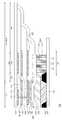
도 2는 본 발명의 실시예에 따른 유기 발광 표시 장치의 표시 패널(200)의, GIP 회로(221)가 배치되어 있는 일측의 단면도이다.2 is a cross-sectional view of one side of the
도 2를 참조하여, 우선 본 발명의 실시예에 따른 유기 발광 표시 장치의 표시 패널(200)이 어떻게 구성되어 있는지 설명하고자 한다.Referring to FIG. 2 , first, a configuration of the
표시 패널(200)은 서로 대향하여 마주보는 하부 기판(211)과 상부 기판(212), 그리고 하부 기판(211)과 상부 기판(212)을 합착하고 고정하는 합착층(270)을 포함한다.The
하부 기판(211)에는 유기 발광 소자(260) 및 화소 구동 회로(222)를 포함하는 다수의 화소가 배치된 표시 영역(A/A)과, 각각의 화소에 연결되는 GIP 회로(221)가 배치된 비표시 영역(NON-A/A)이 정의된다. 비표시 영역(NON-A/A)은 표시 영역(A/A)의 주변에 배치되며, 비표시 영역(NON-A/A)에 의하여 표시 영역(A/A)이 둘러싸일 수 있다.A display area A/A in which a plurality of pixels including an organic
화소 구동 회로(222)와 GIP 회로(221)를 연결하는 더미 배선부(DA)가, 표시 영역(A/A)의 경계와 접하는 비표시 영역(NON-A/A)에 대응하여 배치된다. 그리고, GIP 회로(221)로부터 연장되어 표시 패널(200) 외부에 배치되는 여타 구성 요소들과 연결되는 배선부(WA)가 GIP 회로(221) 옆인, 비표시 영역(NON-A/A)의 최외곽에 대응하여 배치된다.The dummy wiring part DA connecting the
상부 기판(212)에는 표시 영역(A/A)에 대응하여 컬러 필터(280)가 배치된다.A
하부 기판(211)과 상부 기판(212)은 서로 대향하여 포개진다. 이 때, 화소, GIP 회로(221) 및 컬러 필터(280)가 하부 기판(211)과 상부 기판(212) 사이에 모두 배치되도록, 하부 기판(211)과 상부 기판(212)이 서로 대향하여 포개진다.The
합착층(270)은 하부 기판(211)과 상부 기판(212) 사이에 배치되고, 하부 기판(211)과 상부 기판(212)이 서로 합착되도록 하고, 나아가 하부 기판(211)과 상부 기판(212)이 합착된 상태가 영구히 고정되도록 한다. 합착층(270)은 비표시 영역(NON-A/A)에 대응하여 배치된 제1 합착 영역(271)(Dam) 및 제1 합착 영역(271)에 의하여 둘러싸이는 제2 합착 영역(272)(Filling)을 포함한다.The
비표시 영역(NON-A/A)에 대응하여, GIP 회로(221)와 합착층(270) 사이에는, GIP 회로(221)에 포함된 산화물 반도체를 사용하는 TFT를 모두 덮음으로써, 외부로부터 입사되는 자외선을 차단하는 반사층이 배치된다. 그리고, 비표시 영역(NON-A/A)에 대응하여, 반사층과 상부 기판(212) 사이에는 제1 합착 영역(271) 및 제2 합착 영역-노출영역이 배치된다.Corresponding to the non-display area NON-A/A, between the
도 2에 도시된 본 발명의 실시예에 따른 유기 발광 표시 장치는 하부 기판(211) 상에서 발광한 광이 컬러 필터(280)가 배치된 상부 기판(212)을 통해 외부로 방출되는 탑 에미션 방식의 유기 발광 표시 장치일 수 있으나 이는 예시적인 구조일 뿐 본 발명이 이에 제한되는 것은 아니다.The organic light emitting diode display according to the embodiment of the present invention shown in FIG. 2 is a top emission method in which light emitted from a
도 2에는 도시되지 않았으나, GIP 회로(221)는 표시 패널(200)의 일측 뿐만 아니라, 표시 패널(200)의 여타 측에도 추가로 배치될 수 있다. 예를 들어, GIP 회로(221)는 표시 패널(200)의 마주보는 양 측에 배치될 수 있다.Although not shown in FIG. 2 , the
이하에서는 하부 기판(211)과 상부 기판(212) 및 이들 사이에 배치되는 구성 요소들에 대하여 보다 자세히 살펴보고자 한다.Hereinafter, the
하부 기판(211)은 유리 기판이거나 플라스틱 계열의 기판일 수 있다. 유기 발광 표시 장치를 구성하는 각 구성 요소들을 유기 발광 표시 장치에 배치함에 있어서 각 구성 요소들을 고정하고 지지하는 역할을 한다.The
하부 기판(211) 상에 비표시 영역(NON-A/A)에 대응하여 GIP 회로(221)가 배치된다. GIP 회로(221)는 다수의 산화물 반도체를 사용하는 TFT(Oxide TFT)를 포함한다. 산화물 반도체를 사용하는 TFT는 게이트 전극, 게이트 절연층, 산화물 반도체층, 에치 스타퍼, 소스 전극 및 드레인 전극으로 구성된다. 산화물 반도체를 사용하는 TFT에 대하여 이하에서 보다 자세히 살펴 보기로 한다.A
하부 기판(211) 상에 게이트 전극이 배치된다. 게이트 전극은 전도성이 우수한, 금속 또는 금속 합금으로 구성될 수 있다. 예를 들어, 게이트 전극은 몰리브덴(Mo), 텅스텐(W), 백금(Pt), 탄탈(Ta), 알루미늄(Al), 크롬(Cr), 금(Au), 티탄(Ti), 니켈(Ni), 네오디뮴(Nd) 및 구리(Cu) 또는 이들의 합금 중 적어도 어느 하나로 이루어질 수 있으나, 이에 제한되지 않고, 다양한 물질로 형성될 수 있다.A gate electrode is disposed on the
게이트 전극 상에 게이트 절연층이 배치된다. 게이트 절연층은 게이트 전극을 전기적으로 절연시키며, 게이트 전극에 직접 접촉하여 배치된다. 게이트 절연층은, 실리콘 산화물, 실리콘 질화물 또는 금속 산화물로 구성될 수 있다. 구체적으로, 금속 산화물층은 알루미늄 산화물, 아연 산화물, 지르코늄 산화물, 티탄 산화물, 하프늄 산화물, 란타늄 산화물 등 중 하나로 이루어질 수 있다.A gate insulating layer is disposed on the gate electrode. The gate insulating layer electrically insulates the gate electrode and is disposed in direct contact with the gate electrode. The gate insulating layer may be made of silicon oxide, silicon nitride, or metal oxide. Specifically, the metal oxide layer may be formed of one of aluminum oxide, zinc oxide, zirconium oxide, titanium oxide, hafnium oxide, lanthanum oxide, and the like.
게이트 절연층 상에 산화물 반도체층이 배치된다. 산화물 반도체층은 반도체 성질을 가지는, 금속 산화물로 구성될 수 있다. 이 때, 반도체 성질을 가지는 금속 산화물은 인듐 산화물(InO), 주석 산화물(SnO), 아연 산화물(ZnO), 카드뮴 산화물(CdO), 갈륨 산화물(GaO), 하프늄 인듐 아연 산화물(HfInZnO), 인듐 갈륨 아연 산화물(InGaZnO), 인듐 주석 아연 산화물(InSnZnO), 인듐 아연 산화물(InZnO), 주석 아연 산화물(SnZnO) 중 적어도 어느 하나로 이루어질 수 있다. 이 때, 산화물 반도체층의 두께는 약 10 nm 내지 1000 nm 정도의 두께로 형성될 수 있으나, 다양하게 조정될 수 있다.An oxide semiconductor layer is disposed on the gate insulating layer. The oxide semiconductor layer may be composed of a metal oxide, having semiconductor properties. At this time, the metal oxide having semiconductor properties is indium oxide (InO), tin oxide (SnO), zinc oxide (ZnO), cadmium oxide (CdO), gallium oxide (GaO), hafnium indium zinc oxide (HfInZnO), indium gallium It may be formed of at least one of zinc oxide (InGaZnO), indium tin zinc oxide (InSnZnO), indium zinc oxide (InZnO), and tin zinc oxide (SnZnO). In this case, the thickness of the oxide semiconductor layer may be formed to a thickness of about 10 nm to about 1000 nm, but may be variously adjusted.
이 때, 산화물 반도체층이 자외선과 같은 빛에너지에 노출될 경우, 산화물 반도체층이 가지는 산소 빈격자점(Vacancy)에 전자가 트랩(Trap)됨으로써, 산화물 반도체층이 환원되게 된다. 이에 따라, 산화물 반도체층을 사용하는 TFT의 문턱 전압이 음의 바이어스(Negative bias)로 변동이 발생하게 된다. GIP 회로(221)에 포함되는 산화물 반도체층을 사용하는 TFT의 문턱 전압이 변동되면, 각각의 유기 발광 소자(260)를 원하는 대로 구동하지 못하게 됨에 따라 표시 패널(200)의 표시 품질에 이상이 생기고 경우에 따라서는 유기 발광 표시 장치의 불량으로 이어질 수 있다. 따라서, 유기 발광 표시 장치를 제작하는 전 과정에서, GIP 회로(221)에 포함된 산화물 반도체를 사용한 TFT의 문턱 전압 특성이 변동되지 않도록 하는, 유기 발광 표시 장치를 발명하는 것이 필요하다.At this time, when the oxide semiconductor layer is exposed to light energy such as ultraviolet rays, electrons are trapped in oxygen vacancies of the oxide semiconductor layer, thereby reducing the oxide semiconductor layer. Accordingly, the threshold voltage of the TFT using the oxide semiconductor layer is changed with a negative bias. When the threshold voltage of the TFT using the oxide semiconductor layer included in the
산화물 반도체층 상에 에치 스타퍼가 배치된다. 보다 구체적으로, 에치 스타퍼는 산화물 반도체층의 백 채널(Back-channel) 상에서 소스 전극과 드레인 전극 사이에 배치된다. 에치 스타퍼는 절연 물질로 구성된다. 이러한 에치 스타퍼는 산화물 반도체층이 포토 공정에 의해 화학물질과 접촉하는 것을 방지하고, 습식 또는 건식 식각 및 플라즈마 공정 등에 의해 손상되는 것을 방지하는 역할을 한다. 즉, 에치 스타퍼에 의해, 공정 수행 중 발생할 수 있는 산화물 반도체층의 캐리어 농도 변화를 최소화 할 수 있다.An etch stopper is disposed on the oxide semiconductor layer. More specifically, the etch stopper is disposed between the source electrode and the drain electrode on a back-channel of the oxide semiconductor layer. The etch stopper is made of an insulating material. The etch stopper serves to prevent the oxide semiconductor layer from being in contact with a chemical material by a photo process, and from being damaged by a wet or dry etching process and a plasma process. That is, the change in the carrier concentration of the oxide semiconductor layer that may occur during the process may be minimized by the etch stopper.
산화물 반도체층 및 에치 스타퍼 상에 소스 전극 및 드레인 전극이 배치된다. 소스 전극 및 드레인 전극 각각은, 산화물 반도체층과 직접 접촉하는 방식으로 산화물 반도체층과 전기적으로 연결된다. 소스 전극 및 드레인 전극은, 에치 스타퍼 및 산화물 반도체층의 양측 가장자리를 덮는 형태로 배치된다. 소스 전극 및 드레인 전극은 몰리브덴(Mo), 텅스텐(W), 백금(Pt), 탄탈(Ta), 알루미늄(Al), 크롬(Cr), 금(Au), 티탄(Ti), 니켈(Ni), 네오디뮴(Nd) 및 구리(Cu) 또는 이들의 합금 중 적어도 어느 하나로 이루어질 수 있으나, 이에 제한되지 않고, 다양한 물질로 형성될 수 있다.A source electrode and a drain electrode are disposed on the oxide semiconductor layer and the etch stopper. Each of the source electrode and the drain electrode is electrically connected to the oxide semiconductor layer in such a way as to directly contact the oxide semiconductor layer. The source electrode and the drain electrode are disposed to cover both edges of the etch stopper and the oxide semiconductor layer. Source electrode and drain electrode are molybdenum (Mo), tungsten (W), platinum (Pt), tantalum (Ta), aluminum (Al), chromium (Cr), gold (Au), titanium (Ti), nickel (Ni) , neodymium (Nd), copper (Cu), or may be made of at least one of alloys thereof, but is not limited thereto, and may be formed of various materials.
본 명세서에서는 TFT가 인버티드 스태거드(Inverted staggered) 구조인 것으로 설명하였으나 코플래너(Coplanar) 구조의 TFT도 사용될 수 있다.Although it has been described herein that the TFT has an inverted staggered structure, a TFT having a coplanar structure may also be used.
비표시 영역(NON-A/A)의 배선부(WA), GIP 회로(221) 및 더미 배선부(DA)와, 표시 영역(A/A)의 화소 구동 회로(222) 상에 연속적으로 제1 패시베이션층(231)이 배치된다. 제1 패시베이션층(231)은 비표시 영역(NON-A/A)의 배선부(WA), GIP 회로(221) 및 더미 배선부(DA)와, 표시 영역(A/A)의 화소 구동 회로(222) 상면의 형상을 따라 배치된다. 제1 패시베이션층(231)은 산화규소, 질화규소, 산화알루미늄, 산화아연, 산화지르코늄, 산화티타늄, 산화하프늄, 산화란타늄 중에서 적어도 하나의 무기물질로 구성되는 무기층을 포함할 수 있다. 제1 패시베이션층(231)은 스퍼터링(Sputtering) 이나 열 증착(Thermal deposition)과 같은 물리적 기상증착(Physical vapor deposition) 공정 또는 화학적 기상증착(Chemical vapor deposition) 공정에 의해 형성된다. 제1 패시베이션층(231)은 수소, 산소 및 수분으로부터, 비표시 영역(NON-A/A)의 배선부(WA), GIP 회로(221) 및 더미 배선부(DA)와, 표시 영역(A/A)의 화소 구동 회로(222)를 보호하는 역할을 한다. 이를 위해, 제1 패시베이션층(231)은 1 ㎛ 이상 10 ㎛ 이하의 두께로 형성될 수 있다.The wiring portion WA, the
제1 패시베이션층(231) 상에 비표시 영역(NON-A/A)에 대응하여 반사층이, 표시 영역(A/A)에 대응하여 보조 전극이 배치될 수 있다. 이 때, 비표시 영역(NON-A/A)에 대응하여, 제1 패시베이션층(231)과 제1 오버 코팅층(241) 사이에 배치되는 반사층을 제1 반사층(252)이라 한다. 그리고 표시 영역(A/A)에 대응하여, 제1 패시베이션층(231)과 제1 오버 코팅층(241) 사이에 배치되는 보조 전극을 제1 보조 전극(261(a))이라 한다. 이 때, 제1 보조 전극(261(a))은 제1 패시베이션층(231)의 컨택홀 및 제1 오버 코팅층(241)의 컨택홀을 통하여, 유기 발광 소자(260)의 화소 전극(261)과 화소 구동 회로(222)에 포함되어 있는 구동 TFT의 소스 전극 또는 드레인 전극 중 어느 하나가 전기적으로 연결되도록 하는 전극이다.A reflective layer may be disposed on the
제1 반사층(252)은 제1 패시베이션층(231) 상에 배치된다. 이 때, 제1 반사층(252)은 제1 반사층(252) 하에 배치되는 GIP 회로(221)를 덮는 형상으로 배치된다. 보다 구체적으로, 제1 반사층(252)은 GIP 회로(221)에 포함되는 산화물 반도체를 사용하는 TFT를 모두 덮는 형상으로 배치된다. 제1 반사층(252)은 GIP 회로(221)를 가림으로써, GIP 회로(221)에 외부로부터 입사되는 자외선을 차단시키는 역할을 한다. 제1 반사층(252)은 자외선과 같은 빛에너지를 반사시킴으로써 GIP 회로(221)를 빛에너지의 영향으로부터 차단한다.The first
소정의 파장대의 자외선을 반사시키기 위하여, 제1 반사층(252)은 광반사성이 우수한 금속 또는 금속 합금을 포함할 수 있다. 보다 구체적으로 제1 반사층(252)은 은(Ag), 알루미늄(Al), 몰리브덴(Mo) 및 이들의 합금 중 적어도 어느 하나를 포함할 수 있다. 예를 들어, 제1 반사층(252)은 몰리브덴(Mo) - 알루미늄(Al) - 몰리브덴(Mo) 의 삼중층 구조를 가질 수 있다. 제1 반사층(252)이 몰리브덴(Mo) - 알루미늄(Al) - 몰리브덴(Mo) 의 삼중층 구조를 가질 경우 365 nm 파장 영역대의 자외선에 대한 제1 반사층(252)의 투과도를 측정해 본 결과, 두께 100 nm 일 때에는 약 1.3 %, 두께 200 nm 일 때에는 0 %, 두께 400 nm 일 때에는 0 % 이다. 즉, 제1 반사층(252)은 365 nm 파장 영역대의 자외선에 대한 투과도가 0(zero) 수준이 되기 위하여, 적어도 200 nm 이상의 두께를 가지면 충분하다.In order to reflect ultraviolet rays in a predetermined wavelength band, the first
이 때, 제1 반사층(252)을 구성하는 물질과 제1 보조 전극(261(a))을 구성하는 물질이 동일할 수 있다. 또한, 제1 반사층(252)의 두께와 제1 보조 전극(261(a))의 두께가 동일할 수 있다.In this case, the material constituting the first
제1 반사층(252) 및 제1 보조 전극(261(a)) 상에 제1 오버 코팅층(241)이 배치된다. 제1 오버 코팅층(241)은 절연 물질로 형성되고, 1 μm 이상 2 μm 이하의 두께로 형성된다. 예를 들어, 아크릴계 수지, 에폭시 수지, 페놀 수지, 폴리아미드계 수지, 폴리이미드계 수지, 불포화 폴리에스테르계 수지, 폴리페닐렌계 수지, 폴리페닐렌설파이드계 수지, 벤조사이클로부텐 및 포토레지스트 중 하나로 형성될 수 있으나, 이에 제한되지 않는다.A
제1 오버 코팅층(241) 상에 비표시 영역(NON-A/A)에 대응하여 뱅크(243)가 배치되고, 표시 영역(A/A)에 대응하여 유기 발광 소자(260) 및 뱅크(243)가 배치된다. 이렇게 비표시 영역(NON-A/A)에 대응하여, 제1 오버 코팅층(241)과 뱅크(243) 사이에 배치되는 반사층을 제2 반사층(251)이라 한다. 이 때, 유기 발광 소자(260)는 각각의 화소 마다 각각의 화소 구동 회로(222)에 대응하여 배치되며, 유기 발광층(262), 화소 전극(261) 및 공통 전극(263)을 포함한다.A
보다 구체적으로, 제1 오버 코팅층(241) 상에 표시 영역(A/A)에 대응하여 정공(Hole)을 유기 발광층(262)에 공급하는 화소 전극(261)이 각각의 화소마다 독립하여 배치된다. 평면상으로 보았을 때, 아일랜드 형상을 가지는 화소 전극(261)의 가장자리를 둘러서 뱅크(243)가 배치된다. 화소 전극(261) 및 뱅크(243) 상에 유기 발광층(262)이 배치되고, 유기 발광층(262) 상에 전자(Electron)를 유기 발광층(262)에 공급하는 공통 전극(263)이 배치된다.More specifically, a
표시 영역(A/A)에서, 화소 전극(261)의 가장자리를 뱅크(243)가 덮도록, 제1 오버 코팅층(241) 상에 뱅크(243)가 배치됨으로써, 각각의 화소마다 발광 영역이 구획된다. 각각의 화소 별로 각각의 발광 영역은 아일랜드 형상의 화소 전극(261) 중, 뱅크(243)와 중첩되지 않는 화소 전극(261) 영역에 의해 구획된다. 즉, 뱅크(243)가 배치되지 않음으로써 화소 전극(261)이 노출되는 영역이 발광 영역이 된다. 이리하여, 각각의 화소는 각각의 발광 영역과 그 이외의 영역인 비 발광 영역으로 구획된다.In the display area A/A, the
비표시 영역(NON-A/A)에서, 제2 반사층(251)의 전 영역을 뱅크(243)가 덮도록, 제1 오버 코팅층(241) 상에 뱅크(243)가 배치될 수 있다.In the non-display area NON-A/A, the
뱅크(243)는 절연물질로 구성된다. 예를 들어, 뱅크(243)는 폴리이미드와 같은 플라스틱 계열의 물질로 이루어진 투명 레진일 수도 있고, 블랙 카본(Black carbon)을 포함하는 블랙 레진(Black-resin)일 수도 있다. 이 때, 블랙 레진은 예를 들어, PALIOGEN Black L0084(BASF로부터 상업적으로 구입 가능), Pigment Black K801(BASF로부터 상업적으로 구입 가능), REGAL 330(Cabot로부터 상업적으로 구입 가능), Nipex 150(Degusssa로부터 상업적으로 구입 가능), Carbon Black 5250 및 Carbon Black 5750(Columbia Chemical로부터 상업적으로 구입 가능)와 같은, 블랙 카본 등뿐만 아니라 그 혼합물을 포함할 수 있다.The
도 2에서는 화소 전극(261)이 단일층인 것으로 간략히 도시되었으나, 화소 전극(261)은 반사 전극 및 반사 전극 상의 투명 도전층을 포함할 수 있다. 화소 전극(261)의 반사 전극은 광반사성이 우수한 금속 물질로 이루어질 수 있고, 예를 들어, 은(Ag), 알루미늄(Al), 몰리브덴(Mo) 등과 같은 금속 및 이들의 합금 중 적어도 어느 하나를 포함할 수 있다. 화소 전극(261)의 투명 도전층은 일함수가 높은 투명 도전성 산화물(TCO)로 이루어질 수 있고, 예를 들어, 인듐 주석 산화물(InSnO), 인듐 아연 산화물(InZnO) 등과 같은 물질로 이루어질 수 있다.Although the
화소 전극(261)은 제1 오버 코팅층(241)의 컨택홀을 통하여 제1 보조 전극(261(a))과 연결됨으로써, 화소 구동 회로(222)에 포함되어 있는 구동 TFT의 소스 전극 또는 드레인 전극 중 어느 하나와 전기적으로 연결된다.The
제1 오버 코팅층(241) 상에 비표시 영역(NON-A/A)에 대응하여 제2 반사층(251)이 배치된다. 이 때, 제2 반사층(251)은 제2 반사층(251) 하에 배치되는 GIP 회로(221)를 덮는 형상으로 배치된다. 보다 구체적으로, 제2 반사층(251)은 GIP 회로(221)에 포함되는 산화물 반도체를 사용하는 TFT를 모두 덮는 형상으로 배치된다. 제2 반사층(251)은 GIP 회로(221)를 가림으로써, GIP 회로(221)에 외부로부터 입사되는 소정의 파장대의 자외선을 차단시키는 역할을 한다. 제2 반사층(251)은 소정의 파장대의 자외선을 반사시킴으로써 GIP 회로(221)를 자외선의 영향으로부터 차단한다.A second
소정의 파장대의 자외선을 반사시키기 위하여, 제2 반사층(251)은 광반사성이 우수한 금속 또는 금속 합금을 포함할 수 있다. 보다 구체적으로 제2 반사층(251)은 은(Ag), 알루미늄(Al), 몰리브덴(Mo) 및 이들의 합금 중 적어도 어느 하나를 포함할 수 있다. 또한 제2 반사층(251)은 일함수가 높은 투명 도전성 산화물(TCO)을 포함할 수도 있다. 예를 들어, 제2 반사층(251)은 인듐 주석 산화물(InSnO) - 은 합금(Ag alloy) - 인듐 주석 산화물(InSnO)의 삼중층 구조일 수 있다. 제2 반사층(251)이 인듐 주석 산화물(InSnO) - 은 합금(Ag alloy) - 인듐 주석 산화물(InSnO)의 삼중층 구조를 가질 경우 320 nm 파장 영역대의 자외선에 대한 제2 반사층(251)의 투과도를 측정해 본 결과, 두께 100 nm 일 때에는 약 23 %, 두께 200 nm 일 때에는 약 8 %, 두께 400 nm 일 때에는 0 % 이다. 즉, 제2 반사층(251)은 320 nm 파장 영역대의 자외선에 대한 투과도가 0(zero) 수준이 되기 위하여, 적어도 400 nm 이상의 두께를 가지면 충분하다.In order to reflect ultraviolet rays in a predetermined wavelength band, the second
이 때, 제2 반사층(251)을 구성하는 물질과 화소 전극(261)을 구성하는 물질이 동일할 수 있다. 예를 들어, 제2 반사층(251)을 구성하는 물질과 화소 전극(261) 중 반사 전극을 구성하는 물질이 동일할 수 있다. 또한, 제2 반사층(251)의 두께와 화소 전극(261)의 두께가 동일할 수 있다. 예를 들어, 제2 반사층(251)의 두께와 화소 전극(261) 중 반사 전극의 두께가 동일할 수 있다.In this case, the material constituting the second
공통 전극(263)은 광반투과성의 도전층으로 구성된다. 즉, 공통 전극(263)은 유기 발광층(262)에서 발광된 광 중 일부는 통과시켜 외부로 방출되도록 하고, 다른 일부는 화소 전극(261) 방향으로 반사되도록 구성될 수 있다. 구체적으로, 공통 전극(263)은 일함수가 낮은 금속 물질로 형성될 수 있다. 또한 공통 전극(263)은 광투과성을 확보하기 위하여 매우 얇은 두께로 형성될 수 있다. 예를 들어, 공통 전극(263)은 은(Ag), 티타늄(Ti), 알루미늄(Al), 몰리브덴(Mo), 또는 은(Ag)과 마그네슘(Mg)의 합금 등과 같은 금속 물질이 500 Å 보다 작은 두께로 아주 얇게 형성된 반투과층일 수 있다.The
도 2에서는 본 발명의 설명함에 있어서 편의상, 표시 영역(A/A)에 배치되는 다수의 화소들 중, 비표시 영역(NON-A/A)과 가장 인접한 하나의 화소만을 도시하였으나, 하부 기판(211)은 다수의 적색 화소, 녹색 화소 및 청색 화소를 포함한다. 이 때, 적색 화소, 녹색 화소 및 청색 화소는 모두 백색광을 발광하는 유기 발광 소자(260)를 포함할 수 있다. 예를 들어, 유기 발광층(262)이 모든 화소에서 복수 개의 스택(Stack)을 이루고 있고, 각각의 스택에서의 유기 발광층(262)이 보색관계에 있는 색의 광을 각각 발생하여, 이들이 합쳐져 백색광이 구현될 수 있다. 이러한 구조를 취함으로써 유기 발광 소자(260)에서는 백색광이 방출될 수 있다. 또는, 적색 화소는 적색광을 발광하는 유기 발광 소자(260)를 포함하고, 녹색 화소는 녹색광을 발광하는 유기 발광 소자(260)를 포함하고, 청색 화소는 청색광을 발광하는 유기 발광 소자(260)를 포함할 수 있다. 예를 들어, 유기 발광층(262)은 각각의 화소 별로, 적색을 발광하는 적색 유기 발광층(262), 녹색을 발광하는 녹색 유기 발광층(262), 청색을 발광하는 청색 유기 발광층(262)일 수 있다. 경우에 따라서, 하부 기판(211)은 백색광을 발광하는 유기 발광 소자(260)를 포함하는 백색 화소를 더 포함할 수도 있다. 이 때, 하부 기판(211)의 백색 화소에 대응하여서는 컬러 필터부가 배치되지 않을 수도 있다.In FIG. 2 , only one pixel closest to the non-display area NON-A/A is illustrated among a plurality of pixels disposed in the display area A/A for convenience of explanation of the present invention, but the lower substrate ( 211 includes a plurality of red pixels, green pixels, and blue pixels. In this case, the red pixel, the green pixel, and the blue pixel may all include the organic
공통 전극(263) 상에 제2 패시베이션층(232)이 배치된다. 이 때, 제2 패시베이션층(232)은 공통 전극(263) 상면의 형상을 따라 배치된다. 제2 패시베이션층(232)은 산화규소, 질화규소, 산화알루미늄, 산화아연, 산화지르코늄, 산화티타늄, 산화하프늄, 산화란타늄 중에서 적어도 하나의 무기물질로 구성되는 무기층을 포함할 수 있다. 또한 제2 패시베이션층(232)은 이물 방지 및 평탄화 작용을 하는 유기물질로 구성되는 유기층을 포함할 수 있다. 이 때 유기물질은 에폭시, 아크릴레이트 또는 우레탄아크릴레이트를 포함하는 고분자 유기 화합물일 수 있다. 제2 패시베이션층(232)은 산소 및 수분으로부터 유기 발광 소자(260)를 보호하는 역할을 한다. 이를 위해, 제2 패시베이션층(232)은 10㎛ 이하의 두께로 형성될 수 있다. 제2 패시베이션층(232)은 스퍼터링(Sputtering) 이나 열 증착(Thermal Deposition)과 같은 물리적 기상증착(Physical Vapor Deposition) 공정 또는 화학적 기상증착(Chemical Vapor Deposition) 공정에 의해 형성된다.A
합착층(270)은 제2 패시베이션층(232) 상에 배치된다. 합착층(270)은 하부 기판(211)과 상부 기판(212) 사이에 배치되어, 하부 기판(211)과 상부 기판(212)이 결합되도록 한다. 합착층(270)은 비표시 영역(NON-A/A)에 대응하여 배치된 댐(Dam) 역할을 하는 제1 합착 영역(271)을 포함하고, 제1 합착 영역(271)에 의하여 폐쇄적으로 구획된 영역을 채우는(Filling) 역할을 하는 제2 합착 영역(272)을 포함한다. 제1 합착 영역(271)은 비표시 영역(NON-A/A)에 대응되므로 투명할 필요가 없다. 그러나, 제2 합착 영역(272)은 비표시 영역(NON-A/A) 일부에 대응되도록 배치될 수도 있기는 하지만, 표시 영역(A/A) 전체에 대응하여 배치되므로, 반드시 투명하고 광학적으로 깨끗하여야 한다. 또한, 제1 합착 영역(271)의 물질과 제2 합착 영역(272)의 성분 및 조성비가 서로 다를 수 있다. 또한, 제1 합착 영역(271)의 굴절률은 제2 합착 영역(272)의 굴절률과 다를 수 있다.The
컬러 필터(280)는 합착층(270) 상에 표시 영역(A/A)에 대응하여 배치된다. 유기 발광층(262)에서 발생한 광은, 유기 발광 표시 장치의 외부로 방출되는 과정에서 컬러 필터(280)를 통과하게 된다. 도 2에 도시되지는 않았으나, 컬러 필터(280)는 각각의 화소 별로 적색 컬러 필터부, 녹색 컬러 필터부 및 청색 컬러 필터부를 포함할 수 있다. 적색 컬러 필터부는 유기 발광층(262)에서 발광하여 외부로 방출되는 광의 색이 적색이 되도록 하고, 녹색 컬러 필터부는 유기 발광층(262)에서 발광하여 외부로 방출되는 광의 색이 녹색이 되도록 하고, 청색 컬러 필터부는 유기 발광층(262)에서 발광하여 외부로 방출되는 광의 색이 청색이 되도록 한다. 적색 컬러 필터부는 적색 화소에, 녹색 컬러 필터부는 녹색 화소에, 청색 컬러 필터부는 청색 화소에 각각 대응하도록 배치될 수 있다. 즉, 상부 기판(212)의 컬러 필터(280)에는 하부 기판(211)의 적색 화소에 대응하여 적색 컬러 필터부가 배치되고, 하부 기판(211)의 녹색 화소에 대응하여 녹색 컬러 필터부가 배치되고, 하부 기판(211)의 청색 화소에 대응하여 청색 컬러 필터부가 배치될 수 있다. 각각의 컬러 필터부는 비 발광 영역 전 영역 및 발광 영역 전 영역에 대응하도록 배치될 수도 있고, 비 발광 영역의 일부분 및 발광 영역 전 영역에 대응하도록 배치될 수도 있고, 발광 영역 전 영역에만 대응하도록 배치될 수도 있다.The
광흡수부(290)는 인접한 화소 간의 경계에 대응하여 합착층(270) 상에 배치된다. 광흡수부(290)가 인접한 화소 간의 경계에 대응함에 있어, 광흡수부(290)는 해당 화소의 컬러 필터부 상에 배치될 수 있다. 도시되지는 않았으나, 광흡수부(290)가 인접한 화소 간의 경계에 대응함에 있어, 광흡수부(290)는 해당 화소의 컬러 필터부를 둘러싸도록 배치되거나, 해당 화소의 컬러 필터부 하에 배치될 수 있다.The
이 때, 광흡수부(290)의 배치는 발광 영역에 대응하지 않는다. 즉, 광흡수부(290)는 발광 영역 이외의 영역 즉, 비 발광 영역에만 대응하도록 배치된다. 이로써, 광흡수부(290)는 인접한 화소 간에 발생할 수 있는 혼색 현상을 방지한다. 광흡수부(290)가 비 발광 영역에만 대응하도록 배치됨에 따라, 표시 영역(A/A)에서의 광흡수부(290)는 뱅크(243)와 중첩하게 된다. 이 때, 광흡수부(290)와 뱅크(243) 사이에는 합착층(270)이, 특히, 합착층(270) 중에서도 제2 합착 영역(272)이 개재될 수 있다.In this case, the arrangement of the
광흡수부(290)는 블랙매트릭스(Black Matrix)로 구성될 수 있다. 블랙매트릭스는 블랙 카본 또는 각종 색안료의 혼합물 또는 금속 산화물 입자 중 적어도 어느 하나를 포함하는 레진(Resin)으로 구성될 수 있다. 블랙매트릭스는 컬러 필터부 상에 배치되어 있다. 도시되지는 않았으나, 블랙매트릭스는 컬러 필터부 하에 배치될 수도 있다. 즉, 블랙매트릭스와 상부 기판(212) 사이에 컬러 필터부가 배치될 수도 있다. 또한, 도시되지는 않았으나, 블랙매트릭스가 컬러 필터부와 중첩하지 않고 각각의 컬러 필터부 사이 사이에 배치될 수도 있다. 도 2에 도시되지는 않았으나, 블랙매트릭스는 테이퍼 형상을 가질 수도 있고, 역테이퍼 형상을 가질 수도 있다. 블랙매트릭스를 형성하는 포토 리소그래피 공정에서의 노광 및 현상 조건을 조절함으로써 각 블랙매트릭스의 형상을 형성할 수 있다.The
도 2에 도시되지는 않았으나, 광흡수부(290)는 블랙매트릭스로 구성되는 것이 아니라, 각각의 컬러 필터부가 중첩 배치됨으로써 구성될 수 있다. 보다 구체적으로, 광흡수부(290)는 적색 컬러 필터부와 녹색 컬러 필터부가 중첩하여 배치됨으로써 구성될 수 있다. 또한, 광흡수부(290)는 녹색 컬러 필터부와 청색 컬러 필터부가 중첩하여 배치됨으로써 구성될 수 있다. 또한, 청색 컬러 필터부와 적색 컬러 필터부가 중첩하여 배치됨으로써 구성될 수 있다. 또한, 광흡수부(290)는 적색 컬러 필터부, 녹색 컬러 필터부 및 청색 컬러 필터부 모두가 중첩하여 배치됨으로써 구성될 수 있다. 즉, 광흡수부(290)는 적색 컬러 필터부, 녹색 컬러 필터부 및 청색 컬러 필터부 중 적어도 두 개 이상의 컬러 필터부가 중첩하여 배치된 광흡수부(290)일 수 있다.Although not shown in FIG. 2 , the
광흡수부(290)는 비표시 영역(NON-A/A)에까지 일부 연장되어 배치될 수 있다. 이 때, 광흡수부(290)는 제1 합착 영역(271)과 중첩하지 않는다. 즉, 광흡수부(290)는 제2 합착 영역(272)과 상부 기판(212) 사이에 배치될 뿐이고, 제1 합착 영역(271)과 상부 기판(212) 사이에는 배치되지 않는다.The
컬러 필터(280) 상에 상부 기판(212)이 배치된다. 상부 기판(212)의 면적은 하부 기판(211)의 면적보다 작을 수 있다. 또는, 적어도 상부 기판(212)의 면적과 중첩되지 않는, 하부 기판(211)의 일부 면적이 비표시 영역(NON-A/A)에 대응하여 존재할 수 있다. 상부 기판(212)은 투명한 유리 기판이거나, 투명한 플라스틱 계열의 기판일 수 있다.An
이하에서는 레진의 경화 과정을 통하여 합착층(270)을 형성함에 있어서, 동시에 화소의 유기 발광 소자(260)와, GIP 회로(221)의 산화물 반도체를 사용하는 TFT에 손상이 가지 않도록 하는 각 구성 요소들의 배치 관계에 대하여 보다 자세히 살펴보고자 한다.Hereinafter, when the
하부 기판(211)과 상부 기판(212)이 레진에 의한 합착 상태를 유지하도록 고정하기 위해서는, 레진이 경화되어 합착층(270)이 형성되어야 한다. 레진을 경화를 위해서는 고에너지를 가해주는 과정이 필요한데, 이 때 경화용 고에너지로서 열에너지 또는 빛에너지를 이용할 수 있다. 그런데, 유기 발광 소자(260)는, 고열에 의해 변성될 수 있는 유기물질로 이루어진 유기 발광층(262)을 포함하고 있기 때문에 고열이 가해지면 손상에 의한 열화가 진행된다. 이러한 점은 합착층(270)을 형성하기 위한 경화용 고에너지로서, 열에너지를 사용하는데 있어 제약 사항이 된다. 한편, 합착층(270) 상에 배치된 컬러 필터(280)와 합착층(270) 하에 배치된 화소 구동 회로(222)는 표시 패널(200) 내부의 레진으로 빛에너지가 도달하지 못하게끔 차단한다. 즉 컬러 필터(280)와 화소 구동 회로(222)는 합착층(270)을 형성하기 위한 경화용 고에너지로서, 빛에너지를 사용하는데 제약 사항이 된다.In order to fix the
정리하면, 표시 패널(200) 내부의 레진을 경화하여 합착층(270)을 형성함에 있어서, 빛에너지를 사용할 때는 빛에너지가 합착층(270) 전 영역에 균일하게 전달되지 않는다는 문제가 있고, 열에너지를 사용할 때는 고열로 인하여 유기 발광 소자(260)가 손상을 입을 수 있다는 문제가 있다.In summary, in forming the
이에, 비표시 영역(NON-A/A)에 대응하여, 컬러 필터(280) 주변을 둘러싸는 형상을 가지도록 고점도 레진이 배치된다. 이 때, 고점도 레진은 빛에너지로 경화가 되는 물질로 구성된다. 특히, 고점도 레진은 광경화를 위한 광개시제 및 광가교제 및 광반응성 작용기를 가지는 모노머 또는 폴리머를 포함한다.Accordingly, the high-viscosity resin is disposed to have a shape surrounding the
그리고, 표시 영역(A/A)에 대응하여, 컬러 필터(280)를 덮거나 또는 유기 발광 소자(260)를 덮는 형상을 가지도록 저점도 레진이 배치된다. 이 때, 저점도 레진은 열에너지로 경화가 되는 물질로 구성된다.In addition, the low-viscosity resin is disposed to cover the
고점도 레진은 댐(Dam)의 형상을 가짐으로써 저점도 레진이 채워져야 하는 영역을 구획한다. 이 때, 고점도 레진의 점도는 저점도 레진의 점도보다 상대적으로 더 높고, 고점도 레진의 퍼짐성은 저점도 레진의 퍼짐성보다 상대적으로 더 낮다. 이로써 고점도 레진은 상대적으로 퍼짐성이 더 좋은 저점도 레진이 퍼지나가는 영역을 구획하는 울타리, 댐 또는 틀의 역할을 한다.The high-viscosity resin has the shape of a dam, thereby defining an area to be filled with the low-viscosity resin. At this time, the viscosity of the high-viscosity resin is relatively higher than that of the low-viscosity resin, and the spreadability of the high-viscosity resin is relatively lower than that of the low-viscosity resin. In this way, the high-viscosity resin acts as a fence, dam, or frame that divides the area where the low-viscosity resin with relatively better spreadability spreads.
자외선과 같은 빛에너지를 직접적으로 비표시 영역(NON-A/A)에 조사하여, 단시간에 비표시 영역(NON-A/A)에 대응하여 배치된 고점도 레진을 경화한다. 이로써, 제1 합착 영역(271)을 형성한다. 저점도 레진은 빛에너지로 경화가 되는 물질로 구성되지 않을 수 있고, 설사 빛에너지로 경화되는 물질을 일부 포함하고 있다 하더라도 고점도 레진에 비하여 그 양이 현저히 적고, 저점도 레진이 배치된 영역에는 자외선과 같은 빛에너지를 가하지 않음으로써, 고점도 레진이 경화될 때에 저점도 레진은 경화되지 못하고 그대로 유동성을 가진 채로 남아 있게 된다. 고점도 레진이 자외선과 같은 빛에너지에 의하여 경화된 상태인 제1 합착 영역(271)은, 표시 영역(A/A)에 대응하여 배치된 저점도 레진이 마저 경화되어 제2 합착 영역(272)이 되기까지, 저점도 레진의 퍼짐 또는 넘침을 물리적으로 방지하는 울타리, 댐 또는 틀의 역할을 한다.Light energy such as ultraviolet light is directly irradiated to the non-display area NON-A/A to cure the high-viscosity resin disposed corresponding to the non-display area NON-A/A in a short time. Thus, the
열에너지를 직접적으로 표시 패널(200) 전 영역에 가하여, 표시 영역(A/A) 및 비표시 영역(NON-A/A) 일부에 대응하여 배치된 저점도 레진을 경화한다. 열에너지는 열전도 현상에 의하여, 표시 패널(200) 외부에서부터 표시 패널(200) 내부까지 전달이 될 수 있다. 따라서 표시 패널(200) 내부의 표시 영역(A/A)에 대응하는 저점도 레진은 열에너지로 경화가 되는 물질로 구성되는 것이 바람직하다. 저점도 레진의 경화 과정에서, 제1 합착 영역(271)이 저점도 레진의 퍼짐 또는 넘침을 방지하고 있기 때문에, 저점도 레진은 고열의 열에너지로 단시간에 경화될 필요 없이, 상대적으로 저온의 열에너지로 보다 천천히 경화될 수 있다. 이로써 표시 영역(A/A)에 대응하는 합착층(270)이 경화될 때, 유기 발광 소자(260)가 손상되는 문제를 최소화할 수 있다.Heat energy is directly applied to the entire area of the
요약하면, 표시 패널(200)의 외곽부에 해당하고, 비표시 영역(NON-A/A)에 대응되는 제1 합착 영역(271)은 자외선과 같은 빛에너지에 의하여 경화될 수 있는 고점도 레진이 광경화됨으로써 구성된다. 그리고 표시 영역(A/A)에 대응되는 제2 합착 영역(272)은 열에너지에 의하여 경화될 수 있는 저점도 레진이 열경화됨으로써 구성된다. 이에 따라, 고점도 레진은 광개시제, 광가교졔를 포함한다. 저점도 레진 역시 광개시제, 광가교제를 포함할 수 있으나, 고점도 레진이 광개시제, 광가교제를 포함하고 있는 조성비보다 더 적은 조성비를 가질 따름이다.In summary, the
앞서 살펴 보았듯이, 고점도 레진 및 고점도 레진이 광경화된 제1 합착 영역(271)이 배치되는 영역은 비표시 영역(NON-A/A)이다. 고점도 레진은 하부 기판(211) 쪽에서부터 표시 패널(200) 내부를 향하도록 자외선을 조사하여서는 효과적으로 경화될 수 없다. 왜냐하면, 하부 기판(211) 쪽에서부터 표시 패널(200) 내부를 향하도록 자외선과 같은 빛에너지를 조사하는 경우, 비표시 영역(NON-A/A)에 대응하여 배치된 GIP 회로(221) 및 더미 배선부(DA)에 의하여 빛에너지는 차단될 수 밖에 없기 때문이다. 그리고 GIP 회로(221)가 자외선에 의하여 손상이 발생할 수 있다는 문제가 있다. 그러므로, 상부 기판(212) 쪽에서부터 표시 패널(200) 내부를 향하도록 자외선과 같은 빛에너지를 조사하는 것이 바람직하다. 따라서, 컬러 필터(280)를 표시 영역(A/A)에 한정하여 배치하여, 빛에너지가 컬러 필터(280)에 의해 차단되는 일이 없이 고점도 레진으로 도달할 수 있도록 할 필요가 있다.As described above, the high-viscosity resin and the area in which the high-viscosity resin is photocured is disposed in the non-display area NON-A/A. The high-viscosity resin cannot be effectively cured by irradiating ultraviolet rays from the
이 때, 빛에너지가 조사되는 고점도 레진의 표면적이 넓을수록 고점도 레진은 더 빠르게 그리고 더 균일하게 광경화가 진행된다. 따라서, 빛에너지에 노출되는 고점도 레진의 표면적을 넓힐 필요가 있다. 보다 구체적으로는, 고점도 레진의 상면뿐만 아니라 고점도 레진의 측면도 역시 빛에너지에 노출되도록 할 필요가 있다. 저점도 레진에 의해서 형성되는 제2 합착 영역은 투명하고, 광학적으로 깨끗하여야 하므로, 자외선과 같은 빛에너지를 흡수하거나 차단하는 정도가 현저히 떨어진다. 이에 따라, 저점도 레진은 고점도 레진을 경화하기 위한 자외선과 같은 빛에너지를 흡수하거나 차단하지 못하고 그대로 투과하게 된다. 이를 이용하여, 상부 기판(212)과 접하는 고점도 레진의 상면뿐만 아니라, 저점도 레진과 접하는 고점도 레진의 측면도 역시 빛에너지에 노출되도록 한다. 고점도 레진과 인접한 저점도 레진이 광흡수부(290) 및 컬러 필터(280)에 의해 가려지지 않고 그대로 노출되도록 함으로써, 저점도 레진은 고점도 레진을 경화하기 위한 경화용 빛에너지가 고점도 레진의 측면에 전달되도록 하는 매개체 역할을 하게 된다.At this time, the higher the surface area of the high-viscosity resin irradiated with light energy, the faster and more uniformly the high-viscosity resin is photocured. Therefore, it is necessary to increase the surface area of the high-viscosity resin exposed to light energy. More specifically, it is necessary to expose not only the top surface of the high-viscosity resin but also the side surfaces of the high-viscosity resin to light energy. Since the second cementation region formed by the low-viscosity resin must be transparent and optically clean, the degree of absorbing or blocking light energy such as ultraviolet rays is significantly reduced. Accordingly, the low-viscosity resin does not absorb or block light energy such as ultraviolet light for curing the high-viscosity resin, but transmits it as it is. By using this, not only the upper surface of the high-viscosity resin in contact with the
이러한 저점도 레진의 역할을 위하여, 고점도 레진과 인접한 저점도 레진과, 상부 기판(212) 사이에는, 광흡수부(290) 및 컬러 필터(280)가 배치되지 않는다. 이로써 저점도 레진-노출영역이 구성된다. 비표시 영역(NON-A/A)에 대응하여, 고점도 레진과 인접하고, 광흡수부(290) 및 컬러 필터(280)와 중첩하지 않는, 저점도 레진을 저점도 레진-노출영역이라고 명명하기로 한다. 저점도 레진-노출영역은 고점도 레진을 따라, 고점도 레진과 인접하여 배치된다.In order to serve as the low-viscosity resin, the
저점도 레진은 열경화 후에 제2 합착 영역이 된다. 이에 따라, 저점도 레진-노출영역은 열경화 후에 제2 합착 영역-노출영역이 된다. 제1 합착 영역(271)과 인접한 제2 합착 영역(272)과, 상부 기판(212) 사이에는, 광흡수부(290) 및 컬러 필터(280)가 배치되지 않도록 함으로써 제2 합착 영역-노출영역이 구성된다. 비표시 영역(NON-A/A)에 대응하여, 제1 합착 영역(271)과 인접하고, 광흡수부(290) 및 컬러 필터(280)와 중첩하지 않는, 제2 합착 영역(272)을 제2 합착 영역-노출영역이라고 명명하기로 한다. 제2 합착 영역(272)은 제1 합착 영역(271)을 따라 제1 합착 영역(271)과 인접하여 배치된다.The low-viscosity resin becomes the second cementation region after thermosetting. Accordingly, the low-viscosity resin-exposed region becomes the second cemented region-exposed region after thermal curing. The
도 2를 참조하면, 고점도 레진과 광흡수부(290)가 소정 간격 이격하여 구성하는 이격거리 만큼, 저점도 레진이 노출된다. 이 때, 고점도 레진과 광흡수부(290)가 소정 간격 이격하여 이격거리를 구성함으로써, 저점도 레진-노출영역을 매개체로 하여 고점도 레진의 측면이 빛에너지에 노출될 수 있게 된다. 저점도 레진-노출영역은, 고점도 레진과 저점도 레진의 경계에서부터 표시 영역(A/A)을 향하여 제1 폭(W1)을 가지도록 구성된다. 고점도 레진 및 저점도 레진의 경화가 각기 완료되면, 고점도 레진은 제1 합착 영역(271)이, 저점도 레진은 제2 합착 영역(272)이 된다. 따라서, 제1 합착 영역(271)과 제2 합착 영역(272)이 직접 접촉하는 지점으로부터 표시 영역(A/A)을 향하여 제1 폭(W1)을 가지는, 제2 합착 영역-노출영역이 구성된다. 제2 합착 영역-노출영역은 저점도 레진이 열경화되어 형성된 것이므로, 저점도 레진과 마찬가지로, 자외선을 차단하거나 흡수하지 못한다. 즉, 제2 합착 영역-노출영역은 자외선이 투과된다. 이러한 저점도 레진-노출영역 또는 제2 합착 영역-노출영역에 의하여, 고점도 레진의 측면까지도 빛에너지가 조사됨으로써 고점도 레진의 광경화가 보다 효과적으로 일어날 수 있다.Referring to FIG. 2 , the low-viscosity resin is exposed as much as the separation distance formed between the high-viscosity resin and the
제2 합착 영역-노출영역을 배치하여 고점도 레진을 광경화 할 때, 비표시 영역(NON-A/A)에 대응하는 합착층(270), 뱅크(243), 제1 오버 코팅층(241) 등을 투과하여 들어온 자외선과 같은 빛에너지가, GIP 회로(221)에 포함되어 있는 산화물 반도체를 사용하는 TFT를 손상시킬 수 있는 문제가 있다. 보다 구체적으로, 산화물 반도체층이 자외선과 같은 빛에너지에 노출될 경우, 산화물 반도체층이 가지는 산소 빈격자점(Vacancy)에 전자가 트랩(Trap)됨으로써, 산화물 반도체층이 환원되게 된다. 이에 따라, 산화물 반도체층을 사용하는 TFT의 문턱 전압이 음의 바이어스(Negative bias)로 변동이 발생하게 된다. GIP 회로(221)에 포함되는 산화물 반도체층을 사용하는 TFT의 문턱 전압이 변동되면, 각각의 유기 발광 소자(260)를 원하는 대로 구동하지 못하게 됨에 따라 표시 패널(200)의 표시 품질에 이상이 생기고 경우에 따라서는 유기 발광 표시 장치의 불량으로 이어질 수 있다.When the high-viscosity resin is photocured by arranging the second bonding area-exposed area, the
즉, 자외선과 같은 빛에너지가 합착층(270) 형성의 측면에서는 경화용 고에너지로써 꼭 필요한 인자이지만, 반대로 GIP 회로(221)의 산화물 반도체를 사용하는 TFT에는 스트레스를 주는 인자이므로, GIP 회로(221) 상에 배치된 고점도 레진과, GIP 회로(221) 사이에서 자외선과 같은 빛에너지의 진행을 차단하여야 할 필요가 있다.That is, light energy such as ultraviolet light is an essential factor as high energy for curing in terms of forming the
본 발명의 발명자는 상술한 바와 같이 합착층(270) 경화를 위하여 자외선과 같은 빛에너지를 유기 발광 표시 장치에 가할 때 GIP 회로(221)를 보호함으로써, GIP 회로(221)에 포함된 산화물 반도체를 사용한 TFT의 특성이 변동되지 않도록 하는, 유기 발광 표시 장치를 발명하였다. 본 발명의 실시예에 따른 유기 발광 표시 장치에는, 합착층(270) 경화용 고에너지로써 가해지는 자외선과 같은 빛에너지의 영향으로부터 GIP 회로(221)에 포함된 산화물 반도체를 사용한 TFT를 보호하기 위하여, 제1 합착 영역(271) 및 제2 합착 영역-노출영역과 GIP 회로(221) 사이에 자외선을 차단하는 반사층이 배치된다.As described above, the inventor of the present invention protects the
이 때, 제2 합착 영역-노출영역이 가지는 제1 폭(W1)은, 제1 폭(W1)을 포함하는 수직 단면에서 반사층이 가지는 제2 폭(W2)보다 좁다. 그리고 제2 폭(W2)이 제1 폭(W1)을 포개도록, 제2 폭(W2)과 제1 폭(W1)이 중첩한다. 그리고 제2 폭(W2)은, 제2 폭(W2)을 포함하는 수직 단면에서 GIP 회로(221)가 가지는 제3 폭(W3)보다 넓다. 그리고 제2 폭(W2)이 제3 폭(W3)을 포개도록, 제2 폭(W2)과 제 3폭이 중첩한다. 여기서, GIP 회로(221)가 가지는 제3 폭(W3)은, 제2 폭(W2)을 포함하는 수직 단면에서 서로 가장 멀리 떨어져 있는, GIP 회로(221)의 산화물 반도체를 사용하는 TFT를 기준으로 정의되는 폭을 의미한다.In this case, the first width W1 of the second bonding area-exposed area is narrower than the second width W2 of the reflective layer in a vertical section including the first width W1. In addition, the second width W2 and the first width W1 overlap so that the second width W2 overlaps the first width W1 . In addition, the second width W2 is wider than the third width W3 of the
이 때, 제2 합착 영역-노출영역의 평면 형상은 반사층의 평면 형상에 포개지고, 반사층의 평면 면적이 제2 합착 영역-노출영역의 평면 면적보다 크다.In this case, the planar shape of the second cementation area-exposed area is superimposed on the planar shape of the reflective layer, and the planar area of the reflective layer is larger than the planar area of the second cementation area-exposed area.
GIP 회로(221) 상에, GIP 회로(221)에 포함되는 산화물 반도체를 사용하는 TFT를 덮도록 배치되는 반사층은 앞서 살펴 보았듯이 광반사성이 우수한 금속 또는 금속 합금으로 구성될 수 있다. 금속은 도전성을 가지기 때문에 GIP 회로(221)에 영향을 줄 수도 있으나, 제1 패시베이션층(231) 또는 제1 오버 코팅층(241)이 적어도 1 μm 이상의 두께를 가지게 됨에 따라, 제1 패시베이션층(231) 또는 제1 오버 코팅층(241)의 두께만큼 반사층과 GIP 회로(221)의 이격 거리가 확보된다. 따라서 반사층이 GIP 회로(221)의 구동에 영향을 주지 않는다.A reflective layer disposed on the
이 때, 반사층은 제1 반사층(252) 만을 포함하거나, 제2 반사층(251) 만을 포함하거나, 또는 제1 반사층(252) 및 제2 반사층(251)을 모두 포함할 수도 있다.In this case, the reflective layer may include only the first
도 3은 또 다른, 본 발명의 실시예에 따른 유기 발광 표시 장치의 표시 패널(300)의, GIP 회로(221)가 배치되어 있는 일측의 단면도이다.3 is another cross-sectional view of one side of the
도 3의 본 발명의 실시예에 따른 유기 발광 표시 장치의 표시 패널(300)을 설명함에 있어, 도 2의 본 발명의 실시예에 따른 유기 발광 표시 장치의 표시 패널(200)과 동일한 구성 요소에 대해서는 도 2에서 사용한 도면 부호를 동일하게 사용하였으며, 그에 대한 설명을 생략한다. 도 3의 본 발명의 실시예에 따른 유기 발광 표시 장치의 표시 패널(300)을 설명함에 있어, 도 2의 본 발명의 실시예에 따른 유기 발광 표시 장치의 표시 패널(200)에서의 설명과 동일하지 않은 부분을 이하에서 추가로 설명하기로 한다. 특히 합착층(270)을 완전하게 경화함에 있어서, 동시에 화소의 유기 발광 소자(260)와, GIP 회로(221)의 산화물 반도체를 사용하는 TFT에 손상이 가지 않도록 하는 각 구성 요소들의 배치 관계를 중점적으로 추가로 설명하기로 한다.In the description of the
도 3을 참조하면, 빛에너지에 노출되는 고점도 레진의 표면적을 가능한 한 넓히기 위하여, 제1 합착 영역(271)은, 일체화되지 않고 그 사이 사이에 제2 합착 영역(272)을 가지도록 패터닝 될 수 있다. 다시 말하면, 고점도 레진을 형성할 때에, 표면적을 넓히기 위하여, 소정 간격 이격하여 이격거리를 구성하는 패턴을 가지도록 형성할 수 있다. 이로써, 고점도 레진의 측면이 빛에너지에 노출될 수 있게 된다. 이 때, 서로 인접한 고점도 레진 패턴끼리 소정 간격 이격하여 구성하는 이격거리 만큼 채워진 저점도 레진이 노출된다. 이로써, 고점도 레진과 저점도 레진의 경계에서부터 표시 영역(A/A)을 향하여 제1 폭(W1)을 가지는, 저점도 레진-노출영역이 구성된다. 이 때, 고점도 레진 패턴의 형상에 대응하여, 저점도 레진-노출영역은 다수개가 고점도 레진 패턴과 교번하여 배치될 수 있다.Referring to FIG. 3 , in order to increase the surface area of the high-viscosity resin exposed to light energy as much as possible, the
고점도 레진 및 저점도 레진의 경화가 각기 완료되면, 고점도 레진은 제1 합착 영역(271)이, 저점도 레진은 제2 합착 영역(272)이 된다. 따라서, 제1 합착 영역(271)과 제2 합착 영역(272)이 직접 접촉하는 지점으로부터 표시 영역(A/A)을 향하여 제1 폭(W1)을 가지는, 제2 합착 영역-노출영역이 구성된다. 마찬가지로, 제1 합착 영역(271) 패턴의 형상에 대응하여, 제2 합착 영역-노출영역은 다수개가 제1 합착 영역(271) 패턴과 교번하여 배치될 수 있다. 이러한 저점도 레진-노출영역 또는 제2 합착 영역-노출영역의 배치에 의하여, 고점도 레진이 빛에너지에 노출되는 표면적이 증가하여 고점도 레진의 광경화가 보다 효과적으로 일어날 수 있다.When curing of the high-viscosity resin and the low-viscosity resin is completed, the high-viscosity resin becomes the
도 4는 또 다른, 본 발명의 실시예에 따른 유기 발광 표시 장치의 표시 패널(400)에서 GIP 회로(221)가 배치되어 있는 일측의 단면도이다.4 is another cross-sectional view of one side in which the
도 4의 본 발명의 실시예에 따른 유기 발광 표시 장치의 표시 패널(400)을 설명함에 있어, 도 2의 본 발명의 실시예에 따른 유기 발광 표시 장치의 표시 패널(200)과 동일한 구성 요소에 대해서는 도 2에서 사용한 도면 부호를 동일하게 사용하였으며, 그에 대한 설명을 생략한다. 도 4의 본 발명의 실시예에 따른 유기 발광 표시 장치의 표시 패널(400)을 설명함에 있어, 도 2의 본 발명의 실시예에 따른 유기 발광 표시 장치의 표시 패널(200)에서의 설명과 동일하지 않은 부분을 이하에서 추가로 설명하기로 한다.In the description of the
도 4를 참조하면, 제1 패시베이션층(231)과 제1 오버 코팅층(241) 사이에 추가의, 제2 오버 코팅층(242)이 배치된다. 즉, 비표시 영역(NON-A/A)에 대응하여 배치된 배선부(WA), GIP 회로(221) 및 더미 배선부(DA)와 표시 영역(A/A)에 대응하여 배치된 화소 구동 회로(222) 상에 제1 패시베이션층(231), 제2 오버 코팅층(242) 그리고 제1 오버 코팅층(241)이 순차로 배치된다.Referring to FIG. 4 , an additional, second over-coating layer 242 is disposed between the
제2 오버 코팅층(242)은 절연 물질로 형성되고, 1 μm 이상 2 μm 이하의 두께로 형성된다. 예를 들어, 아크릴계 수지, 에폭시 수지, 페놀 수지, 폴리아미드계 수지, 폴리이미드계 수지, 불포화 폴리에스테르계 수지, 폴리페닐렌계 수지, 폴리페닐렌설파이드계 수지, 벤조사이클로부텐 및 포토레지스트 중 하나로 형성될 수 있으나, 이에 제한되지 않는다. 제2 오버 코팅층(242)을 구성하는 물질은 제1 오버 코팅층(241)을 구성하는 물질과 동일할 수 있다.The second overcoat layer 242 is formed of an insulating material and has a thickness of 1 μm or more and 2 μm or less. For example, formed of one of an acrylic resin, an epoxy resin, a phenol resin, a polyamide-based resin, a polyimide-based resin, an unsaturated polyester-based resin, a polyphenylene-based resin, a polyphenylene sulfide-based resin, benzocyclobutene, and a photoresist may be, but is not limited thereto. The material constituting the second overcoat layer 242 may be the same as the material constituting the
제1 패시베이션층(231)과 제2 오버 코팅층(242) 사이에 비표시 영역(NON-A/A)에 대응하여 반사층이 배치되고 표시 영역(A/A)에 대응하여 보조 전극이 배치된다. 이렇게 비표시 영역(NON-A/A)에 대응하여, 제1 패시베이션층(231)과 제2 오버 코팅층(242) 사이에 배치되는 반사층을 제3 반사층(253)이라 한다. 그리고 표시 영역(A/A)에 대응하여 제1 패시베이션층(231)과 제2 오버 코팅층(242) 사이에 배치되는 보조 전극을 제2 보조 전극(261(b))이라 한다. 이 때, 제2 보조 전극(261(b))은 제1 패시베이션층(231)의 컨택홀을 통하여 화소 구동 회로(222)에 포함되어 있는 구동 TFT의 소스 전극 또는 드레인 전극 중 어느 하나와 연결되고, 제2 오버 코팅층(242)의 컨택홀을 통하여 제1 보조 전극(261(a))과 연결된다. 이로써, 제2 보조 전극(261(b))은 유기 발광 소자(260)의 화소 전극(261)과 화소 구동 회로(222)에 포함되어 있는 구동 TFT의 소스 전극 또는 드레인 전극 중 어느 하나가 전기적으로 연결되도록 한다.A reflective layer is disposed between the
제3 반사층(253)은 제1 패시베이션층(231)과 제2 오버 코팅층(242) 사이에 배치된다. 이 때, 제3 반사층(253)은 제3 반사층(253) 하에 배치되는 GIP 회로(221)를 덮는 형상으로 배치된다. 보다 구체적으로, 제3 반사층(253)은 GIP 회로(221)에 포함되는 산화물 반도체를 포함하는 TFT를 모두 덮는 형상으로 배치된다. 제3 반사층(253)은 GIP 회로(221)를 가림으로써, GIP 회로(221)에 외부로부터 입사되는 소정의 파장대의 자외선을 차단시키는 역할을 한다. 제3 반사층(253)은 소정의 파장대의 자외선을 반사시킴으로써 GIP 회로(221)를 자외선의 영향으로부터 차단한다.The third
소정의 파장대의 자외선을 반사시키기 위하여, 제3 반사층(253)은 광반사성이 우수한 금속 또는 금속 합금을 포함할 수 있다. 보다 구체적으로 제3 반사층(253)은 알루미늄, 몰리브덴 및 이들의 합금 중 적어도 어느 하나를 포함할 수 있다. 예를 들어, 제3 반사층(253)은 몰리브덴(Mo) - 알루미늄(Al) - 몰리브덴(Mo)의 삼중층 구조를 가질 수 있다. 제3 반사층(253)이 몰리브덴(Mo) - 알루미늄(Al) - 몰리브덴(Mo)의 삼중층 구조를 가질 경우 365 nm 파장 영역대의 자외선에 대한 제3 반사층(253)의 투과도를 측정해본 결과, 두께 100 nm 일 때에는 약 1.3 %, 두께 200 nm 일 때에는 0 %, 두께 400 nm 일 때에는 0 % 이다. 즉, 제3 반사층(253)은 365 nm 파장 영역대의 자외선에 대한 투과도가 0(zero) 수준이 되기 위하여, 적어도 200 nm 이상의 두께를 가지면 충분하다.In order to reflect ultraviolet rays in a predetermined wavelength band, the third
이 때, 제3 반사층(253)을 구성하는 물질과 제2 보조 전극(261(b))을 구성하는 물질이 동일할 수 있다. 또한, 제3 반사층(253)의 두께와 제2 보조 전극(261(b))의 두께가 동일할 수 있다.In this case, the material constituting the third
제3 반사층(253) 및 제2 보조 전극(261(b)) 상에 제2 오버 코팅층(242)이 배치된다. 그리고 제2 오버 코팅층(242) 상에 비표시 영역(NON-A/A)에 대응하여 제1 반사층(252)이 배치되고 표시 영역(A/A)에 대응하여 제1 보조 전극(261(a))이 배치된다. 그리고 제1 반사층(252)과 제1 보조 전극(261(a)) 상에 제1 오버 코팅층(241)이 배치된다.A second overcoat layer 242 is disposed on the third
여기서, 제1 보조 전극(261(a))은 제2 오버 코팅층(242)의 컨택홀을 통하여 제2 보조 전극(261(b))과 연결되고, 제1 오버 코팅층(241)의 컨택홀을 통하여 유기 발광 소자(260)의 화소 전극(261)과 연결된다. 이로써, 제1 보조 전극(261(a))은 유기 발광 소자(260)의 화소 전극(261)과 화소 구동 회로(222)에 포함되어 있는 구동 TFT의 소스 전극 또는 드레인 전극 중 어느 하나가 전기적으로 연결되도록 한다.Here, the first auxiliary electrode 261 (a) is connected to the second auxiliary electrode 261 (b) through the contact hole of the second over-coating layer 242, and is connected to the contact hole of the first
이 때, 반사층은 제1 반사층(252) 만을 포함하거나, 제2 반사층(251) 만을 포함하거나, 제3 반사층(253) 만을 포함하거나, 제1 반사층(252) 및 제2 반사층(251) 만을 포함하거나, 제2 반사층(251) 및 제3 반사층(253) 만을 포함하거나, 제1 반사층(252) 및 제3 반사층(253) 만을 포함하거나, 또는 제1 반사층(252)과 제2 반사층(251)과 제3 반사층(253)을 모두 포함할 수도 있다.In this case, the reflective layer includes only the first
이상 첨부된 도면을 참조하여 본 발명의 실시예를 더욱 상세하게 설명하였으나, 본 발명은 반드시 이러한 실시예로 국한되는 것은 아니고, 본 발명의 기술사상을 벗어나지 않는 범위 내에서 다양하게 서로 조합되고 변형되어 실시될 수 있다. 따라서, 본 발명에 개시된 실시예들은 본 발명의 기술 사상을 한정하기 위한 것이 아니라 설명하기 위한 것이고, 이러한 실시예에 의하여 본 발명의 기술 사상의 범위가 한정되는 것은 아니다. 본 발명의 보호 범위는 아래의 청구범위에 의하여 해석되어야 하며, 그와 동등한 범위 내에 있는 모든 기술 사상은 본 발명의 권리범위에 포함되는 것으로 해석되어야 할 것이다.Although the embodiments of the present invention have been described in more detail with reference to the accompanying drawings, the present invention is not necessarily limited to these embodiments, and various combinations and modifications are made without departing from the technical spirit of the present invention. can be carried out. Therefore, the embodiments disclosed in the present invention are not intended to limit the technical spirit of the present invention, but to explain, and the scope of the technical spirit of the present invention is not limited by these embodiments. The protection scope of the present invention should be construed by the following claims, and all technical ideas within the scope equivalent thereto should be construed as being included in the scope of the present invention.
200, 300, 400: 표시 패널
A/A: 표시 영역
NON-A/A: 비표시 영역
DA: 더미 배선부
GIP: GIP 회로
WA: 배선부
211: 하부 기판
212: 상부 기판
221: GIP 회로
222: 화소 구동 회로
231: 제1 패시베이션층
232: 제2 패시베이션층
241: 제1 오버 코팅층
242: 제2 오버 코팅층
243: 뱅크
251: 제2 반사층
252: 제1 반사층
253: 제3 반사층
260: 유기 발광 소자
261: 화소 전극
262: 유기 발광층
263: 공통 전극
270, 370: 합착층
271, 371: 제1 합착 영역
272, 372: 제2 합착 영역
280: 컬러 필터
290: 광흡수부200, 300, 400: display panel
A/A: display area
NON-A/A: non-display area
DA: dummy wiring part
GIP: GIP circuit
WA: wiring part
211: lower substrate
212: upper substrate
221: GIP circuit
222: pixel driving circuit
231: first passivation layer
232: second passivation layer
241: first overcoat layer
242: second over-coating layer
243: bank
251: second reflective layer
252: first reflective layer
253: third reflective layer
260: organic light emitting device
261: pixel electrode
262: organic light emitting layer
263: common electrode
270, 370: cementation layer
271, 371: first cementation region
272, 372: second cementation region
280: color filter
290: light absorption unit
Claims (20)
Translated fromKorean상기 하부 기판과 서로 대향하고, 상기 표시 영역에 대응하여 컬러 필터가 배치된 상부 기판,
상기 하부 기판과 상기 상부 기판 사이에 배치되고, 상기 비표시 영역에 대응하여 배치된 제1 합착 영역 및 상기 제1 합착 영역에 의하여 둘러싸이는 제2 합착 영역을 포함하는 합착층 및,
상기 화소 구동 회로 및 상기 GIP 회로 상에 순차로 배치된 제1 패시베이션층, 제1 오버 코팅층 및 뱅크를 포함하고,
상기 제2 합착 영역은, 상기 비표시 영역에 대응하여, 상기 제1 합착 영역과 상기 제2 합착 영역이 직접 접촉하는 지점으로부터 상기 표시 영역을 향하여 제1 폭을 가지는, 제2 합착 영역-노출영역을 가지고,
상기 비표시 영역에 대응하여, 상기 GIP 회로와 상기 합착층 사이에, 자외선을 반사하는 복수의 반사층이 상기 제1 패시베이션층, 제1 오버 코팅층 및 뱅크로 이루어진 군에서 적어도 두 개 사이에 배치되고, 상기 복수의 반사층은 플로팅되며,
상기 복수의 반사층은 제1 패시베이션층과 상기 제1 오버 코팅층 사이에 배치된 제1 반사층 및 상기 제1 오버 코팅층과 상기 뱅크 사이에 배치된 제2 반사층을 포함하는, 유기 발광 표시 장치.A lower substrate in which a display area including a plurality of pixels including an organic light emitting device and a pixel driving circuit is disposed, and a non-display area connected to each pixel and in which a GIP circuit including a TFT using an oxide semiconductor is disposed;
an upper substrate facing the lower substrate and having a color filter disposed to correspond to the display area;
a junction layer disposed between the lower substrate and the upper substrate and including a first junction region disposed to correspond to the non-display region and a second junction region surrounded by the first junction region;
a first passivation layer, a first overcoat layer, and a bank sequentially disposed on the pixel driving circuit and the GIP circuit;
The second junction region may correspond to the non-display region and may have a first width toward the display region from a point where the first junction region and the second junction region are in direct contact with each other. To have,
Corresponding to the non-display area, between the GIP circuit and the bonding layer, a plurality of reflective layers for reflecting ultraviolet rays are disposed between at least two from the group consisting of the first passivation layer, the first overcoat layer, and the bank, The plurality of reflective layers are floating,
The plurality of reflective layers includes a first reflective layer disposed between a first passivation layer and the first over-coating layer, and a second reflective layer disposed between the first over-coating layer and the bank.
상기 제1 합착 영역은 상기 자외선에 의하여 경화된, 제1 합착 영역인 것을 특징으로 하는 유기 발광 표시 장치.According to claim 1,
The organic light emitting diode display according to claim 1, wherein the first bonding area is a first bonding area cured by the ultraviolet light.
상기 제1 합착 영역은 광중합체를 포함하는 것을 특징으로 하는 유기 발광 표시 장치.According to claim 1,
The organic light emitting display device of claim 1, wherein the first bonding region includes a photopolymer.
상기 제2 합착 영역은 자외선이 투과되는 것을 특징으로 하는 유기 발광 표시 장치.According to claim 1,
The organic light emitting display device, characterized in that the second bonding region transmits ultraviolet rays.
상기 제2 합착 영역의 굴절률은 상기 제1 합착 영역의 굴절률과 다른 것을 특징으로 하는 유기 발광 표시 장치.According to claim 1,
The organic light emitting diode display device of claim 1, wherein a refractive index of the second junction region is different from a refractive index of the first junction region.
상기 복수의 반사층은 상기 GIP 회로에 포함된 상기 산화물 반도체를 사용하는 TFT를 모두 덮는 것을 특징으로 하는 유기 발광 표시 장치.According to claim 1,
and the plurality of reflective layers cover all of the TFTs using the oxide semiconductor included in the GIP circuit.
상기 제1 반사층을 구성하는 물질은
상기 표시 영역에 대응하여, 상기 제1 패시베이션층과 상기 제1 오버 코팅층 사이에 배치된 제1 보조 전극을 구성하는 물질과 동일한 것을 특징으로 하는 유기 발광 표시 장치.According to claim 1,
The material constituting the first reflective layer is
The organic light emitting diode display according to claim 1, wherein the same material as the material constituting the first auxiliary electrode disposed between the first passivation layer and the first over-coating layer corresponds to the display area.
상기 제1 반사층의 두께는
상기 표시 영역에 대응하여, 상기 제1 패시베이션층과 상기 제1 오버 코팅층 사이에 배치된 제1 보조 전극의 두께와 동일한 것을 특징으로 하는 유기 발광 표시 장치.2. The method of claim 1
The thickness of the first reflective layer is
The organic light emitting diode display according to claim 1 , wherein the thickness of the first auxiliary electrode disposed between the first passivation layer and the first overcoat layer is the same as that of the first auxiliary electrode corresponding to the display area.
상기 제2 반사층을 구성하는 물질은
상기 제1 오버 코팅층 상에 배치된 상기 유기 발광 소자에 포함된 화소 전극을 구성하는 물질과 동일한 것을 특징으로 하는 유기 발광 표시 장치.According to claim 1,
The material constituting the second reflective layer is
The organic light emitting diode display device according to claim 1, wherein the material is the same as the material constituting the pixel electrode included in the organic light emitting device disposed on the first overcoat layer.
상기 제2 반사층의 두께는
상기 제1 오버 코팅층 상에 배치된 상기 유기 발광 소자에 포함된 화소 전극의 두께와 동일한 것을 특징으로 하는 유기 발광 표시 장치.According to claim 1,
The thickness of the second reflective layer is
The organic light emitting display device of claim 1, wherein the thickness of the pixel electrode included in the organic light emitting device disposed on the first overcoat layer is the same.
상기 제1 패시베이션층과 상기 제1 오버 코팅층 사이에 제2 오버 코팅층을 더 포함하고,
상기 복수의 반사층은
상기 제1 패시베이션층과 상기 제2 오버 코팅층 사이에 배치된 제3 반사층을 더 포함하는 것을 특징으로 하는 유기 발광 표시 장치.According to claim 1,
a second overcoat layer between the first passivation layer and the first overcoat layer;
The plurality of reflective layers
and a third reflective layer disposed between the first passivation layer and the second overcoat layer.
상기 제3 반사층을 구성하는 물질은
상기 표시 영역에 대응하여, 상기 제1 패시베이션층과 상기 제2 오버 코팅층 사이에 배치된 제2 보조 전극을 구성하는 물질과 동일한 것을 특징으로 하는 유기 발광 표시 장치.15. The method of claim 14,
The material constituting the third reflective layer is
The organic light emitting diode display according to claim 1 , wherein the material is the same as the material constituting the second auxiliary electrode disposed between the first passivation layer and the second overcoat layer to correspond to the display area.
상기 제3 반사층의 두께는
상기 표시 영역에 대응하여, 상기 제1 패시베이션층과 상기 제2 오버 코팅층 사이에 배치된 제2 보조 전극의 두께와 동일한 것을 특징으로 하는 유기 발광 표시 장치.15. The method of claim 14,
The thickness of the third reflective layer is
and a thickness of a second auxiliary electrode disposed between the first passivation layer and the second over-coating layer to correspond to the display area.
상기 제2 합착 영역-노출영역은 상기 제1 합착 영역에 인접하여 상기 제1 합착 영역을 따라서 배치되고, 상기 제1 폭은 상기 제1 폭을 포함하는 수직 단면에서 상기 복수의 반사층이 가지는 제2 폭보다 좁고, 상기 제2 폭이 상기 제1 폭을 포개도록 상기 제2 폭과 상기 제1 폭이 중첩하는 것을 특징으로 하는 유기 발광 표시 장치.According to claim 1,
The second cementation region-exposed region is disposed along the first cementation region adjacent to the first cementation region, and the first width is a second portion of the plurality of reflective layers in a vertical cross-section including the first width. The organic light emitting diode display device of claim 1, wherein the second width overlaps the first width so that the second width overlaps the first width.
상기 제2 합착 영역-노출영역의 평면 형상은 상기 복수의 반사층의 평면 형상에 포개지고, 상기 복수의 반사층의 평면 면적이 상기 제2 합착 영역-노출영역의 평면 면적보다 큰 것을 특징으로 하는 유기 발광 표시 장치.18. The method of claim 17,
The planar shape of the second junction area-exposed area is superimposed on the planar shape of the plurality of reflective layers, and the planar area of the plurality of reflective layers is larger than the planar area of the second cementation area-exposed area. display device.
상기 제2 폭은, 상기 제1 폭을 포함하는 수직 단면에서 상기 GIP 회로가 가지는 제3 폭보다 넓고,
상기 제2 폭이 상기 제3 폭을 포개도록 상기 제2 폭과 상기 제 3폭이 중첩하는 것을 특징으로 하는 유기 발광 표시 장치.18. The method of claim 17,
The second width is wider than a third width of the GIP circuit in a vertical section including the first width,
The organic light emitting diode display device of claim 1, wherein the second width and the third width overlap so that the second width overlaps the third width.
상기 제1 합착 영역은 사이 사이에 제2 합착 영역을 가지도록 패터닝 되고, 상기 제1 합착 영역의 패턴의 형상에 대응하여, 상기 제2 합착 영역-노출영역은 다수개가 제1 합착 영역 패턴과 교번하여 배치되는 것을 특징으로 하는 유기 발광 표시 장치.According to claim 1,
The first cementation region is patterned to have a second cementation region therebetween, and a plurality of the second cementation region-exposed regions alternate with the first cementation region pattern to correspond to the shape of the pattern of the first cementation region. An organic light emitting display device, characterized in that it is disposed.
Priority Applications (1)
| Application Number | Priority Date | Filing Date | Title |
|---|---|---|---|
| KR1020140193876AKR102342804B1 (en) | 2014-12-30 | 2014-12-30 | Organic light emitting display device |
Applications Claiming Priority (1)
| Application Number | Priority Date | Filing Date | Title |
|---|---|---|---|
| KR1020140193876AKR102342804B1 (en) | 2014-12-30 | 2014-12-30 | Organic light emitting display device |
Publications (2)
| Publication Number | Publication Date |
|---|---|
| KR20160080987A KR20160080987A (en) | 2016-07-08 |
| KR102342804B1true KR102342804B1 (en) | 2021-12-22 |
Family
ID=56503299
Family Applications (1)
| Application Number | Title | Priority Date | Filing Date |
|---|---|---|---|
| KR1020140193876AActiveKR102342804B1 (en) | 2014-12-30 | 2014-12-30 | Organic light emitting display device |
Country Status (1)
| Country | Link |
|---|---|
| KR (1) | KR102342804B1 (en) |
Families Citing this family (4)
| Publication number | Priority date | Publication date | Assignee | Title |
|---|---|---|---|---|
| KR102728403B1 (en)* | 2017-02-24 | 2024-11-12 | 삼성디스플레이 주식회사 | Organic light emitting display device |
| KR102473378B1 (en)* | 2017-08-31 | 2022-12-01 | 엘지디스플레이 주식회사 | Organic light emitting display device |
| KR102461393B1 (en)* | 2017-11-29 | 2022-10-31 | 엘지디스플레이 주식회사 | Display apparatus having a light-emitting device |
| KR102433198B1 (en)* | 2017-12-12 | 2022-08-16 | 엘지디스플레이 주식회사 | Organic light emitting display device |
Citations (1)
| Publication number | Priority date | Publication date | Assignee | Title |
|---|---|---|---|---|
| US20050040762A1 (en)* | 2002-12-26 | 2005-02-24 | Semiconductor Energy Laboratory Co., Ltd. | Light emitting device and method for manufacturing the same |
Family Cites Families (3)
| Publication number | Priority date | Publication date | Assignee | Title |
|---|---|---|---|---|
| KR20060031590A (en)* | 2005-01-04 | 2006-04-12 | 후지 덴키 홀딩스 가부시키가이샤 | Organic EL display and manufacturing method |
| CN105070749B (en)* | 2009-07-18 | 2019-08-09 | 株式会社半导体能源研究所 | Semiconductor device and method of manufacturing semiconductor device |
| JP6074597B2 (en)* | 2013-03-29 | 2017-02-08 | 株式会社Joled | Organic EL display device and electronic device |
- 2014
- 2014-12-30KRKR1020140193876Apatent/KR102342804B1/enactiveActive
Patent Citations (1)
| Publication number | Priority date | Publication date | Assignee | Title |
|---|---|---|---|---|
| US20050040762A1 (en)* | 2002-12-26 | 2005-02-24 | Semiconductor Energy Laboratory Co., Ltd. | Light emitting device and method for manufacturing the same |
Also Published As
| Publication number | Publication date |
|---|---|
| KR20160080987A (en) | 2016-07-08 |
Similar Documents
| Publication | Publication Date | Title |
|---|---|---|
| KR102735475B1 (en) | Light emitting display device | |
| KR102478641B1 (en) | Organic light emitting display device | |
| US9601554B2 (en) | Transparent display device and method of manufacturing the same | |
| JP7045889B2 (en) | Display device and its manufacturing method | |
| KR101765102B1 (en) | Organic light emitting display device and method of manufacturing the same | |
| US11437439B2 (en) | Display device | |
| US10032809B2 (en) | Method of manufacturing display device including light blocking portion on planarization layer protrusion | |
| US10515609B2 (en) | Display device and operation method thereof, and electronic device | |
| US10032837B2 (en) | Organic electroluminescent display device with enhanced extraction efficiency | |
| JP2018055099A (en) | Display device | |
| US20230309336A1 (en) | Display device | |
| US10942410B2 (en) | Display device and manufacturing method thereof | |
| KR102342804B1 (en) | Organic light emitting display device | |
| JP6132924B2 (en) | Display device | |
| KR102302661B1 (en) | Display Device | |
| CN112530976A (en) | Organic light emitting diode display device | |
| CN120390560A (en) | Display device and method of manufacturing the same | |
| WO2020100862A1 (en) | Display device and method for manufacturing same, electronic device, and illumination device | |
| CN118946206A (en) | Display device and method of manufacturing the same | |
| KR20220080923A (en) | Electroluminescence Display | |
| KR102394349B1 (en) | Display device and method for manufacturing thereof | |
| KR102428392B1 (en) | Organic Light Emitting Diode Display Device | |
| JP2020181696A (en) | Organic electroluminescence display device | |
| US20250275439A1 (en) | Display Device | |
| KR20250104805A (en) | Display apparatus |
Legal Events
| Date | Code | Title | Description |
|---|---|---|---|
| PA0109 | Patent application | Patent event code:PA01091R01D Comment text:Patent Application Patent event date:20141230 | |
| PG1501 | Laying open of application | ||
| A201 | Request for examination | ||
| PA0201 | Request for examination | Patent event code:PA02012R01D Patent event date:20191226 Comment text:Request for Examination of Application Patent event code:PA02011R01I Patent event date:20141230 Comment text:Patent Application | |
| E902 | Notification of reason for refusal | ||
| PE0902 | Notice of grounds for rejection | Comment text:Notification of reason for refusal Patent event date:20210420 Patent event code:PE09021S01D | |
| AMND | Amendment | ||
| E601 | Decision to refuse application | ||
| PE0601 | Decision on rejection of patent | Patent event date:20211012 Comment text:Decision to Refuse Application Patent event code:PE06012S01D Patent event date:20210420 Comment text:Notification of reason for refusal Patent event code:PE06011S01I | |
| AMND | Amendment | ||
| PX0901 | Re-examination | Patent event code:PX09011S01I Patent event date:20211012 Comment text:Decision to Refuse Application Patent event code:PX09012R01I Patent event date:20210604 Comment text:Amendment to Specification, etc. | |
| PX0701 | Decision of registration after re-examination | Patent event date:20211125 Comment text:Decision to Grant Registration Patent event code:PX07013S01D Patent event date:20211112 Comment text:Amendment to Specification, etc. Patent event code:PX07012R01I Patent event date:20211012 Comment text:Decision to Refuse Application Patent event code:PX07011S01I Patent event date:20210604 Comment text:Amendment to Specification, etc. Patent event code:PX07012R01I | |
| X701 | Decision to grant (after re-examination) | ||
| GRNT | Written decision to grant | ||
| PR0701 | Registration of establishment | Comment text:Registration of Establishment Patent event date:20211220 Patent event code:PR07011E01D | |
| PR1002 | Payment of registration fee | Payment date:20211220 End annual number:3 Start annual number:1 | |
| PG1601 | Publication of registration | ||
| PR1001 | Payment of annual fee | Payment date:20241118 Start annual number:4 End annual number:4 |