KR102341741B1 - Logic circuit, processing unit, electronic component, and electronic device - Google Patents
Logic circuit, processing unit, electronic component, and electronic deviceDownload PDFInfo
- Publication number
- KR102341741B1 KR102341741B1KR1020177008142AKR20177008142AKR102341741B1KR 102341741 B1KR102341741 B1KR 102341741B1KR 1020177008142 AKR1020177008142 AKR 1020177008142AKR 20177008142 AKR20177008142 AKR 20177008142AKR 102341741 B1KR102341741 B1KR 102341741B1
- Authority
- KR
- South Korea
- Prior art keywords
- circuit
- transistor
- layer
- terminal
- oxide
- Prior art date
- Legal status (The legal status is an assumption and is not a legal conclusion. Google has not performed a legal analysis and makes no representation as to the accuracy of the status listed.)
- Active
Links
Images


Classifications
- H—ELECTRICITY
- H03—ELECTRONIC CIRCUITRY
- H03K—PULSE TECHNIQUE
- H03K19/00—Logic circuits, i.e. having at least two inputs acting on one output; Inverting circuits
- H03K19/0008—Arrangements for reducing power consumption
- G—PHYSICS
- G11—INFORMATION STORAGE
- G11C—STATIC STORES
- G11C7/00—Arrangements for writing information into, or reading information out from, a digital store
- G11C7/04—Arrangements for writing information into, or reading information out from, a digital store with means for avoiding disturbances due to temperature effects
- H01L27/1207—
- H01L27/1255—
- H01L28/40—
- H01L29/045—
- H01L29/7849—
- H—ELECTRICITY
- H03—ELECTRONIC CIRCUITRY
- H03K—PULSE TECHNIQUE
- H03K19/00—Logic circuits, i.e. having at least two inputs acting on one output; Inverting circuits
- H03K19/0175—Coupling arrangements; Interface arrangements
- H03K19/0185—Coupling arrangements; Interface arrangements using field effect transistors only
- H03K19/018507—Interface arrangements
- H03K19/018514—Interface arrangements with at least one differential stage
- H—ELECTRICITY
- H10—SEMICONDUCTOR DEVICES; ELECTRIC SOLID-STATE DEVICES NOT OTHERWISE PROVIDED FOR
- H10D—INORGANIC ELECTRIC SEMICONDUCTOR DEVICES
- H10D1/00—Resistors, capacitors or inductors
- H10D1/60—Capacitors
- H10D1/68—Capacitors having no potential barriers
- H—ELECTRICITY
- H10—SEMICONDUCTOR DEVICES; ELECTRIC SOLID-STATE DEVICES NOT OTHERWISE PROVIDED FOR
- H10D—INORGANIC ELECTRIC SEMICONDUCTOR DEVICES
- H10D30/00—Field-effect transistors [FET]
- H10D30/60—Insulated-gate field-effect transistors [IGFET]
- H10D30/67—Thin-film transistors [TFT]
- H10D30/6729—Thin-film transistors [TFT] characterised by the electrodes
- H10D30/673—Thin-film transistors [TFT] characterised by the electrodes characterised by the shapes, relative sizes or dispositions of the gate electrodes
- H10D30/6733—Multi-gate TFTs
- H10D30/6734—Multi-gate TFTs having gate electrodes arranged on both top and bottom sides of the channel, e.g. dual-gate TFTs
- H—ELECTRICITY
- H10—SEMICONDUCTOR DEVICES; ELECTRIC SOLID-STATE DEVICES NOT OTHERWISE PROVIDED FOR
- H10D—INORGANIC ELECTRIC SEMICONDUCTOR DEVICES
- H10D30/00—Field-effect transistors [FET]
- H10D30/60—Insulated-gate field-effect transistors [IGFET]
- H10D30/67—Thin-film transistors [TFT]
- H10D30/6757—Thin-film transistors [TFT] characterised by the structure of the channel, e.g. transverse or longitudinal shape or doping profile
- H—ELECTRICITY
- H10—SEMICONDUCTOR DEVICES; ELECTRIC SOLID-STATE DEVICES NOT OTHERWISE PROVIDED FOR
- H10D—INORGANIC ELECTRIC SEMICONDUCTOR DEVICES
- H10D30/00—Field-effect transistors [FET]
- H10D30/60—Insulated-gate field-effect transistors [IGFET]
- H10D30/791—Arrangements for exerting mechanical stress on the crystal lattice of the channel regions
- H10D30/798—Arrangements for exerting mechanical stress on the crystal lattice of the channel regions being provided in or under the channel regions
- H—ELECTRICITY
- H10—SEMICONDUCTOR DEVICES; ELECTRIC SOLID-STATE DEVICES NOT OTHERWISE PROVIDED FOR
- H10D—INORGANIC ELECTRIC SEMICONDUCTOR DEVICES
- H10D62/00—Semiconductor bodies, or regions thereof, of devices having potential barriers
- H10D62/40—Crystalline structures
- H—ELECTRICITY
- H10—SEMICONDUCTOR DEVICES; ELECTRIC SOLID-STATE DEVICES NOT OTHERWISE PROVIDED FOR
- H10D—INORGANIC ELECTRIC SEMICONDUCTOR DEVICES
- H10D62/00—Semiconductor bodies, or regions thereof, of devices having potential barriers
- H10D62/40—Crystalline structures
- H10D62/405—Orientations of crystalline planes
- H—ELECTRICITY
- H10—SEMICONDUCTOR DEVICES; ELECTRIC SOLID-STATE DEVICES NOT OTHERWISE PROVIDED FOR
- H10D—INORGANIC ELECTRIC SEMICONDUCTOR DEVICES
- H10D86/00—Integrated devices formed in or on insulating or conducting substrates, e.g. formed in silicon-on-insulator [SOI] substrates or on stainless steel or glass substrates
- H10D86/40—Integrated devices formed in or on insulating or conducting substrates, e.g. formed in silicon-on-insulator [SOI] substrates or on stainless steel or glass substrates characterised by multiple TFTs
- H10D86/421—Integrated devices formed in or on insulating or conducting substrates, e.g. formed in silicon-on-insulator [SOI] substrates or on stainless steel or glass substrates characterised by multiple TFTs having a particular composition, shape or crystalline structure of the active layer
- H10D86/423—Integrated devices formed in or on insulating or conducting substrates, e.g. formed in silicon-on-insulator [SOI] substrates or on stainless steel or glass substrates characterised by multiple TFTs having a particular composition, shape or crystalline structure of the active layer comprising semiconductor materials not belonging to the Group IV, e.g. InGaZnO
- H—ELECTRICITY
- H10—SEMICONDUCTOR DEVICES; ELECTRIC SOLID-STATE DEVICES NOT OTHERWISE PROVIDED FOR
- H10D—INORGANIC ELECTRIC SEMICONDUCTOR DEVICES
- H10D86/00—Integrated devices formed in or on insulating or conducting substrates, e.g. formed in silicon-on-insulator [SOI] substrates or on stainless steel or glass substrates
- H10D86/40—Integrated devices formed in or on insulating or conducting substrates, e.g. formed in silicon-on-insulator [SOI] substrates or on stainless steel or glass substrates characterised by multiple TFTs
- H10D86/481—Integrated devices formed in or on insulating or conducting substrates, e.g. formed in silicon-on-insulator [SOI] substrates or on stainless steel or glass substrates characterised by multiple TFTs integrated with passive devices, e.g. auxiliary capacitors
- H—ELECTRICITY
- H10—SEMICONDUCTOR DEVICES; ELECTRIC SOLID-STATE DEVICES NOT OTHERWISE PROVIDED FOR
- H10D—INORGANIC ELECTRIC SEMICONDUCTOR DEVICES
- H10D86/00—Integrated devices formed in or on insulating or conducting substrates, e.g. formed in silicon-on-insulator [SOI] substrates or on stainless steel or glass substrates
- H10D86/40—Integrated devices formed in or on insulating or conducting substrates, e.g. formed in silicon-on-insulator [SOI] substrates or on stainless steel or glass substrates characterised by multiple TFTs
- H10D86/60—Integrated devices formed in or on insulating or conducting substrates, e.g. formed in silicon-on-insulator [SOI] substrates or on stainless steel or glass substrates characterised by multiple TFTs wherein the TFTs are in active matrices
- H—ELECTRICITY
- H10—SEMICONDUCTOR DEVICES; ELECTRIC SOLID-STATE DEVICES NOT OTHERWISE PROVIDED FOR
- H10D—INORGANIC ELECTRIC SEMICONDUCTOR DEVICES
- H10D87/00—Integrated devices comprising both bulk components and either SOI or SOS components on the same substrate
Landscapes
- Engineering & Computer Science (AREA)
- Computer Hardware Design (AREA)
- Computing Systems (AREA)
- General Engineering & Computer Science (AREA)
- Mathematical Physics (AREA)
- Physics & Mathematics (AREA)
- Thin Film Transistor (AREA)
- Semiconductor Integrated Circuits (AREA)
- Power Engineering (AREA)
- Chemical & Material Sciences (AREA)
- Crystallography & Structural Chemistry (AREA)
- Logic Circuits (AREA)
- Electronic Switches (AREA)
- Design And Manufacture Of Integrated Circuits (AREA)
- Metal-Oxide And Bipolar Metal-Oxide Semiconductor Integrated Circuits (AREA)
- Oscillators With Electromechanical Resonators (AREA)
- Filters And Equalizers (AREA)
Abstract
Translated fromKoreanDescription
Translated fromKorean본 명세서, 도면, 및 청구항(이하에서는 "본 명세서 등"이라고 함)에 개시(開示)되는 본 발명의 일 형태는 반도체 장치(예를 들어 순서 회로, 유지 회로, 저장 회로, 또는 논리 회로), 이의 구동 방법, 및 이의 제작 방법에 관한 것이다. 본 발명의 일 형태는 상술한 기술분야에 한정되지 않는다. 예를 들어 본 발명의 일 형태는 저장 장치, 처리 유닛, 촬상 장치, 표시 장치, 발광 장치, 전기 저장 장치, 이들의 구동 방법, 또는 이들의 제작 방법에 관한 것이다.One embodiment of the present invention disclosed in this specification, drawings, and claims (hereinafter referred to as "this specification, etc.") is a semiconductor device (eg, a sequence circuit, a holding circuit, a storage circuit, or a logic circuit); It relates to a driving method thereof, and a manufacturing method thereof. One embodiment of the present invention is not limited to the technical field described above. For example, one embodiment of the present invention relates to a storage device, a processing unit, an imaging device, a display device, a light emitting device, an electric storage device, a driving method thereof, or a manufacturing method thereof.
반도체 장치의 소비전력을 저감시키기 위하여, 동작할 필요가 없는 회로들은 파워 게이팅 또는 클록 게이팅에 의하여 정지된다. 플립플롭(FF)은 반도체 장치에 많이 포함되는 순서 회로(상태를 유지하는 저장 회로)이다. 따라서, FF의 소비전력 저감은 FF를 포함하는 반도체 장치의 소비전력 저감으로 이어진다. 일반적인 FF는 전원이 차단되면, 유지된 상태(데이터)가 손실된다.In order to reduce power consumption of the semiconductor device, circuits that do not need to operate are stopped by power gating or clock gating. The flip-flop FF is a sequence circuit (a storage circuit that maintains a state) frequently included in semiconductor devices. Accordingly, the reduction in power consumption of the FF leads to a reduction in power consumption of the semiconductor device including the FF. In general FF, when the power is cut off, the maintained state (data) is lost.
반도체 영역이 산화물 반도체를 사용하여 형성된 트랜지스터(이하에서 이러한 트랜지스터를 OS 트랜지스터라고 할 수 있음)의 오프 전류가 매우 낮다는 것을 이용함으로써, 전원이 차단되더라도 데이터를 유지할 수 있는 유지 회로가 제안되고 있다. 예를 들어, 특허문헌 1 내지 3의 각각은, OS 트랜지스터를 포함하는 유지 회로를 포함하고 파워 게이팅이 가능한 FF를 개시한다. 비특허문헌 1은 예를 들어, OS 트랜지스터를 포함하는 유지 회로를 FF 및 SRAM의 각각에 사용함에 의한 프로세서의 파워 게이팅을 개시한다.A holding circuit capable of retaining data even when the power is cut off has been proposed by utilizing the very low off current of a transistor in which a semiconductor region is formed using an oxide semiconductor (hereinafter, such a transistor may be referred to as an OS transistor). For example, each of
본 발명의 일 형태의 한 목적은 신규 반도체 장치, 또는 그 반도체 장치의 신규 구동 방법을 제공하는 것이다. 본 발명의 일 형태의 다른 목적은 예를 들어, 파워 게이팅을 수행하는 것, 전원 공급 없이 데이터 유지를 수행하는 것, 소비전력을 저감시키는 것, 사이즈를 축소시키는 것, 또는 설계를 용이하게 하는 것이다.One object of one embodiment of the present invention is to provide a novel semiconductor device or a novel driving method of the semiconductor device. Another object of one aspect of the present invention is, for example, to perform power gating, perform data retention without power supply, reduce power consumption, reduce size, or facilitate design .
복수의 목적의 기재는 각 목적의 존재를 방해하지 않는다. 본 발명의 일 형태는 상술한 목적 모두를 반드시 달성할 필요는 없다. 다른 목적은 본 명세서 등의 기재로부터 명백해질 것이고, 이러한 목적도 본 발명의 일 형태의 목적이 될 수 있다.The description of a plurality of purposes does not prevent the existence of each purpose. One embodiment of the present invention does not necessarily achieve all of the above-described objects. Other objects will become apparent from the description of the present specification and the like, and these objects may also become objects of one embodiment of the present invention.
본 발명의 일 형태는 제 1 회로 및 제 2 회로를 포함하는 논리 회로이다. 제 1 회로는 제 1 내지 제n 입력 단자(n은 2 이상의 정수(integer)) 및 제 1 출력 단자를 포함한다. 제 2 회로는 제 (n+1) 입력 단자, 제 1 노드, 제 1 용량 소자, 및 제 1 내지 제 3 트랜지스터를 포함한다. 제 1 회로는 제 1 내지 제n 입력 단자 중 어느 하나를 선택하고, 선택한 입력 단자의 논리와 같은 논리의 데이터를 제 1 출력 단자로부터 출력하는 기능을 갖는다. 용량 소자는 제 1 노드에 전기적으로 접속된다. 제 1 트랜지스터는 제 (n+1) 입력 단자와 제 1 입력 단자 사이의 전기적 접속을 제어하는 기능을 갖는다. 제 2 트랜지스터는 제 1 출력 단자와 제 1 노드 사이의 전기적 접속을 제어하는 기능을 갖는다. 제 3 트랜지스터는 제 1 노드와 제 1 입력 단자 사이의 전기적 접속을 제어하는 기능을 갖는다. 제 1 트랜지스터의 게이트는 제 2 트랜지스터의 게이트에 전기적으로 접속된다. 제 2 트랜지스터 및 제 3 트랜지스터의 각각은 산화물 반도체층을 사용하여 형성된 반도체 영역을 포함한다.One embodiment of the present invention is a logic circuit including a first circuit and a second circuit. The first circuit includes first ton-th input terminals (n is an integer greater than or equal to 2) and a first output terminal. The second circuit includes a (n +1)th input terminal, a first node, a first capacitive element, and first to third transistors. The first circuit has a functionof selecting any one of the first to nth input terminals and outputting, from the first output terminal, data having the same logic as the logic of the selected input terminal. The capacitive element is electrically connected to the first node. The first transistor has a function of controlling an electrical connection betweenthe (n+1)th input terminal and the first input terminal. The second transistor has a function of controlling an electrical connection between the first output terminal and the first node. The third transistor has a function of controlling an electrical connection between the first node and the first input terminal. The gate of the first transistor is electrically connected to the gate of the second transistor. Each of the second transistor and the third transistor includes a semiconductor region formed using an oxide semiconductor layer.
상술한 형태에 있어서, 제 1 용량 소자 및 제 1 내지 제 3 트랜지스터는 제 1 회로가 형성되는 영역 위에 적층되어도 좋다. 상술한 형태에 있어서, 제 1 트랜지스터는 산화물 반도체층을 사용하여 형성된 반도체 영역을 포함하여도 좋다. 이 경우, 제 1 내지 제 3 트랜지스터의 산화물 반도체층의 각각은 c축 배향된 결정을 포함하는 것이 바람직하다.In the above aspect, the first capacitor element and the first to third transistors may be stacked over the region where the first circuit is formed. In the above aspect, the first transistor may include a semiconductor region formed using an oxide semiconductor layer. In this case, each of the oxide semiconductor layers of the first to third transistors preferably includes a c-axis oriented crystal.
상술한 형태의 논리 회로에서, 제 1 회로는 선택 회로 및 제 1 논리 회로를 포함하여도 좋다. 제 1 논리 회로는 제 (n+2) 입력 단자 및 제 1 출력 단자를 포함하여도 좋다. 제 1 논리 회로는 제 (n+2) 입력 단자의 논리와 같은 논리의 데이터를 제 1 출력 단자로부터 출력하는 기능을 가져도 좋다. 선택 회로는 제 2 출력 단자를 포함하여도 좋다. 선택 회로는 제 1 내지 제n 입력 단자 중 어느 하나와 제 2 출력 단자를 전기적으로 접속시키는 기능을 가져도 좋다. 제 2 출력 단자는 제 (n+2) 입력 단자에 전기적으로 접속되어도 좋다.In the logic circuit of the above type, the first circuit may include a selection circuit and a first logic circuit. The first logic circuit may include a (n +2)th input terminal and a first output terminal. The first logic circuit may have a function of outputting, from the first output terminal, data of the same logic as thatof the (n +2)th input terminal. The selection circuit may include a second output terminal. The selection circuit may havea function of electrically connecting any one of the first to nth input terminals and the second output terminal. The second output terminal may be electrically connected tothe (n +2)th input terminal.
본 발명의 일 형태는 신규 반도체 장치, 또는 그 반도체 장치의 신규 동작 방법을 제공할 수 있다. 또는 본 발명의 일 형태는 파워 게이팅이 가능하고, 전원 공급 없이 데이터 유지가 가능하고, 소비전력을 저감시킬 수 있고, 사이즈를 축소시킬 수 있고, 또는 설계를 용이하게 할 수 있다.One embodiment of the present invention can provide a novel semiconductor device or a novel operating method of the semiconductor device. Alternatively, in one embodiment of the present invention, power gating is possible, data can be maintained without power supply, power consumption can be reduced, size can be reduced, or design can be facilitated.
복수의 효과의 기재는 다른 효과의 존재를 방해하지 않는다. 본 발명의 일 형태에서는 상술한 효과 모두를 얻을 필요는 없다. 본 발명의 일 형태에서는, 명세서 및 도면의 기재로부터 다른 목적, 효과, 및 신규 특징이 명백해질 것이다.The description of a plurality of effects does not prevent the existence of other effects. In one embodiment of the present invention, it is not necessary to obtain all of the above-described effects. In one embodiment of the present invention, other objects, effects, and novel features will become apparent from description of the specification and drawings.
첨부 도면에 있어서,
도 1의 (A)는 논리 회로의 구조예를 도시한 블록도이고, 도 1의 (B)는 도 1의 (A)의 회로(10)의 구조예를 도시한 블록도.
도 2의 (A) 및 (B)는 논리 회로의 구조예를 각각 도시한 블록도.
도 3은 논리 회로의 구조예를 도시한 블록도.
도 4는 스캔 FF(SFF)의 구조예를 도시한 회로도.
도 5는 SFF의 구조예를 도시한 회로도.
도 6은 SFF의 동작예를 도시한 타이밍 차트.
도 7은 SFF의 동작예를 도시한 타이밍 차트.
도 8은 SFF의 구조예를 도시한 회로도.
도 9는 SFF의 구조예를 도시한 회로도.
도 10은 SFF의 구조예를 도시한 회로도.
도 11은 SFF의 구조예를 도시한 회로도.
도 12는 SFF의 구조예를 도시한 회로도.
도 13은 처리 유닛의 구조예를 도시한 블록도.
도 14는 프로세서 코어의 구조예를 도시한 블록도.
도 15는 SFF의 디바이스 구조를 도시한 도면.
도 16의 (A)는 전자 부품의 제작 방법의 예를 나타낸 흐름도이고, 도 16의 (B)는 전자 부품의 구조예를 도시한 개략 투시도.
도 17의 (A) 내지 (F)의 각각은 전자 기기의 예를 도시한 도면.
도 18의 (A)는 트랜지스터의 구조예를 도시한 평면도이고, 도 18의 (B) 내지 (D)는 도 18의 (A)의 트랜지스터의 단면도.
도 19의 (A)는 도 18의 (B)의 트랜지스터의 부분 확대도이고, 도 19의 (B)는 트랜지스터의 에너지 밴드도.
도 20의 (A) 내지 (C)는 트랜지스터의 구조예를 각각 도시한 단면도.
도 21의 (A) 및 (B)는 트랜지스터의 구조예를 각각 도시한 단면도.
도 22는 칩의 구조예를 도시한 단면도.
도 23은 칩의 구조예를 도시한 단면도.In the accompanying drawings,
Fig. 1A is a block diagram showing a structural example of a logic circuit, and Fig. 1B is a block diagram showing a structural example of the
2A and 2B are block diagrams each showing a structural example of a logic circuit.
Fig. 3 is a block diagram showing a structural example of a logic circuit;
Fig. 4 is a circuit diagram showing a structural example of a scan FF (SFF);
Fig. 5 is a circuit diagram showing a structural example of an SFF;
Fig. 6 is a timing chart showing an operation example of the SFF;
Fig. 7 is a timing chart showing an operation example of the SFF;
Fig. 8 is a circuit diagram showing a structural example of an SFF;
Fig. 9 is a circuit diagram showing a structural example of an SFF;
Fig. 10 is a circuit diagram showing a structural example of an SFF;
Fig. 11 is a circuit diagram showing a structural example of an SFF;
Fig. 12 is a circuit diagram showing a structural example of an SFF;
Fig. 13 is a block diagram showing a structural example of a processing unit;
Fig. 14 is a block diagram showing a structural example of a processor core;
Fig. 15 is a diagram showing a device structure of an SFF;
Fig. 16A is a flowchart showing an example of a method for manufacturing an electronic component, and Fig. 16B is a schematic perspective view showing a structural example of the electronic component.
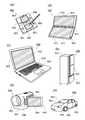
Each of FIGS. 17A to 17F is a diagram showing an example of an electronic device.
Fig. 18A is a plan view showing a structural example of the transistor, and Figs. 18B to 18D are cross-sectional views of the transistor of Fig. 18A.
19A is a partially enlarged view of the transistor of FIG. 18B, and FIG. 19B is an energy band diagram of the transistor.
20A to 20C are cross-sectional views each showing a structural example of a transistor.
21A and 21B are cross-sectional views each showing a structural example of a transistor;
Fig. 22 is a cross-sectional view showing a structural example of a chip;
Fig. 23 is a cross-sectional view showing a structural example of a chip;
본 명세서 등에 있어서, 반도체 장치란, 반도체 특성을 이용하는 장치를 말하고, 반도체 소자(예를 들어, 트랜지스터 또는 다이오드)를 포함하는 회로, 및 이 회로를 포함하는 장치 등을 의미한다. 반도체 장치란, 반도체 특성을 이용함으로써 기능할 수 있는 어떤 장치도 의미한다. 예를 들어, 집적 회로, 및 집적 회로를 포함하는 칩은 모두 반도체 장치이다. 또한, 저장 장치, 표시 장치, 발광 장치, 조명 장치, 및 전자 기기 등은 이들 자체가 반도체 장치일 수 있거나, 또는 각각이 반도체 장치를 포함할 수 있다.In this specification and the like, the term "semiconductor device" refers to a device using semiconductor characteristics, and refers to a circuit including a semiconductor element (eg, a transistor or a diode), a device including the circuit, and the like. A semiconductor device means any device that can function by using semiconductor characteristics. For example, integrated circuits, and chips including integrated circuits, are all semiconductor devices. In addition, the storage device, the display device, the light emitting device, the lighting device, and the electronic device may themselves be semiconductor devices, or may each include a semiconductor device.
본 명세서 등에서 "X와Y가 접속된다"라는 명시적인 기재는X와Y가 전기적으로 접속되는 것,X와Y가 기능적으로 접속되는 것, 그리고X와Y가 직접 접속되는 것을 의미한다. 따라서, 소정의 접속 관계, 예를 들어, 도면 또는 문장에 나타낸 접속 관계에 한정되지 않으며, 도면 또는 문장에는 다른 접속 관계도 포함된다.X 및Y는 각각 물체(예를 들어 장치, 소자, 회로, 배선, 전극, 단자, 도전막, 또는 층)를 나타낸다.In this specification, etc., the explicit description "X andY are connected" means thatX andY are electrically connected, thatX andY are functionally connected, and thatX andY are directly connected. Therefore, it is not limited to a predetermined connection relationship, for example, a connection relationship shown in a drawing or text, and other connection relationships are also included in the drawing or text.X andY each represent an object (eg, a device, element, circuit, wiring, electrode, terminal, conductive film, or layer).
트랜지스터는 3개의 단자(게이트, 소스, 및 드레인)를 갖는 소자이다. 게이트는 트랜지스터의 도통 상태를 제어하기 위한 제어 노드로서 기능한다. 트랜지스터의 형태 또는 단자에 인가되는 전위의 레벨에 따라, 2개의 입출력 노드 중 한쪽이 소스로서 기능하고 다른 쪽이 드레인으로서 기능한다. 따라서, 본 명세서 등에서 "소스" 및 "드레인"이라는 용어는 서로 바뀔 수 있다. 본 명세서 등에서, 게이트 외의 2개의 단자를 제 1 단자 및 제 2 단자라고 하는 경우가 있다.A transistor is a device with three terminals (gate, source, and drain). The gate functions as a control node for controlling the conduction state of the transistor. Depending on the shape of the transistor or the level of the potential applied to the terminals, one of the two input/output nodes functions as a source and the other functions as a drain. Accordingly, the terms “source” and “drain” may be used interchangeably in this specification and the like. In this specification and the like, two terminals other than the gate are sometimes referred to as a first terminal and a second terminal.
노드는, 회로 구조 및 디바이스 구조 등에 따라, 단자, 배선, 전극, 도전층, 도전체, 또는 불순물 영역 등이라고 할 수 있다. 또한, 단자 또는 배선 등을 노드라고 할 수 있다.A node may be said to be a terminal, a wiring, an electrode, a conductive layer, a conductor, an impurity region, etc. according to a circuit structure, a device structure, etc. In addition, a terminal or wiring may be referred to as a node.
또한 전압은 소정의 전위와 참조 전위(예를 들어 접지 전위(GND) 또는 소스 전위) 사이의 전위차를 말하는 경우가 많다. 전압을 전위라고 할 수 있다. 또한 전위는 상대적인 값을 갖는다. 따라서, 접지 전위는 반드시 0V를 의미할 필요는 없다.In addition, the voltage often refers to a potential difference between a predetermined potential and a reference potential (eg, the ground potential (GND) or the source potential). Voltage can be called potential. Also, the potential has a relative value. Therefore, the ground potential does not necessarily mean 0V.
본 명세서 등에서, "막" 및 "층"이라는 용어는 상황 또는 조건에 따라 서로 바뀔 수 있다. 예를 들어, "도전층"이라는 용어는 "도전막"이라는 용어로 바뀔 수 있는 경우가 있다. 예를 들어, "절연막"이라는 용어는 "절연층"이라는 용어로 바뀔 수 있는 경우가 있다.In this specification and the like, the terms “film” and “layer” may be interchanged with each other depending on circumstances or conditions. For example, the term "conductive layer" may be interchanged with the term "conductive film". For example, the term "insulating film" may be changed to the term "insulating layer" in some cases.
본 명세서 등에서, "제 1", "제 2", 및 "제 3" 등의 서수사는 구성요소 간의 혼동을 피하기 위하여 사용되기 때문에, 구성요소의 수 또는 순서를 한정하지 않는다.In this specification and the like, ordinal numbers such as "first", "second", and "third" are used to avoid confusion between the elements, and thus the number or order of the elements is not limited.
본 명세서 등에서, 클록 신호(CLK)를 "신호(CLK)" 또는 "CLK" 등으로 생략하는 경우가 있다. 다른 구성요소(예를 들어 신호, 전압, 전위, 회로, 소자, 전극, 및 배선)에 대해서도 마찬가지이다.In this specification and the like, the clock signal CLK is sometimes omitted as “signal CLK” or “CLK”. The same is true for other components (eg, signals, voltages, potentials, circuits, elements, electrodes, and wirings).
도면에서, 사이즈, 층 두께, 또는 영역은 명료화를 위하여 과장되어 있는 경우가 있다. 따라서, 본 발명의 실시형태들은 그 스케일에 한정되지 않는다. 또한, 도면은 이상적인 예를 나타내는 개략도이고, 본 발명의 실시형태들은 도면에 나타낸 형상 또는 값에 한정되지 않는다. 예를 들어, 노이즈 또는 타이밍 차이로 인한 신호, 전압, 또는 전류의 편차가 포함될 수 있다.In the drawings, sizes, layer thicknesses, or regions are sometimes exaggerated for clarity. Accordingly, embodiments of the present invention are not limited to that scale. In addition, the drawings are schematic diagrams showing ideal examples, and embodiments of the present invention are not limited to the shapes or values shown in the drawings. For example, variations in signal, voltage, or current due to noise or timing differences may be included.
본 명세서에서, "위" 및 "아래" 등의 배치를 설명하는 용어는 도면을 참조하여 구성요소들 사이의 위치 관계를 설명하기 위하여 편의상 사용되는 경우가 있다. 또한, 구성요소들 사이의 위치 관계는 각 구성요소를 설명하는 방향에 따라 적절히 변화된다. 따라서, 본 명세서에서 사용되는 용어에 한정은 없고, 상황에 따라 적절히 설명할 수 있다.In this specification, terms describing the arrangement such as "above" and "below" are sometimes used for convenience to describe the positional relationship between components with reference to the drawings. In addition, the positional relationship between the components is appropriately changed depending on the direction in which each component is described. Therefore, there is no limitation on the terms used in this specification, and may be appropriately described according to circumstances.
블록도에서의 회로 블록들의 위치 관계는 설명을 위하여 특정된다. 상이한 기능들이 상이한 회로 블록들에 의하여 실현되도록 블록도가 나타내더라도, 실제로는 하나의 블록이 상이한 기능들을 실현할 수도 있다. 회로 블록들의 기능은 설명을 위하여 특정된다. 하나의 회로 블록이 도시되더라도, 실제의 회로 블록에서는 하나의 블록에 의하여 수행되는 처리가 복수의 회로 블록에 의하여 수행되는 것처럼 블록들이 제공될 수 있다.Positional relationships of circuit blocks in the block diagram are specified for explanation. Although the block diagram shows that different functions are realized by different circuit blocks, in reality, one block may realize different functions. The function of the circuit blocks is specified for purposes of illustration. Although one circuit block is shown, in an actual circuit block, blocks may be provided as if processing performed by one block is performed by a plurality of circuit blocks.
본 발명의 실시형태에 대하여 이하에서 설명한다. 또한 본 명세서에 기재되는 실시형태들 중 어느 것을 적절히 조합할 수 있다. 또한, 하나의 실시형태에 복수의 구조예(동작예 및 제작 방법예를 포함함)가 제시되는 경우에는, 이들 구조예 중 어느 것을 적절히 조합할 수 있다. 본 발명은 다양한 형태로 실시될 수 있고, 본 발명의 취지 및 그 범위에서 일탈하지 않고 본 발명의 형태 및 상세한 사항을 다양하게 수정할 수 있다는 것은 통상의 기술자에 의하여 용이하게 이해될 것이다. 그러므로, 본 발명은 이하의 실시형태의 설명에 한정하여 해석되지 말아야 한다.EMBODIMENT OF THE INVENTION Embodiment of this invention is described below. Also, any of the embodiments described herein may be appropriately combined. In addition, when a plurality of structural examples (including operation examples and production method examples) are presented in one embodiment, any of these structural examples can be appropriately combined. It will be readily understood by those skilled in the art that the present invention may be embodied in various forms, and that various modifications may be made in the form and details of the present invention without departing from the spirit and scope of the present invention. Therefore, the present invention should not be construed as being limited to the description of the embodiments below.
(실시형태 1)(Embodiment 1)
<논리 회로의 구조예><Structure example of logic circuit>
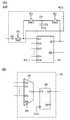
도 1의 (A)는 논리 회로의 구조예를 도시한 것이다. 도 1의 (A)의 논리 회로(100)는 데이터(상태)를 유지할 수 있는 반도체 장치이다. 회로 구조 등에 따라, 논리 회로(100)는 순서 회로라고도 할 수 있다. 논리 회로(100)는 클록 게이팅 및 파워 게이팅이 가능한 반도체 장치이다. 논리 회로(100)는 회로(10) 및 회로(RC1)를 포함한다. 회로(RC1)는 데이터를 유지하는 기능을 갖는 유지 회로이다. 회로(RC1)는 회로(10)의 데이터(상태)를 판독하고 유지하는 기능을 갖는다. 또한, 회로(RC1)는 유지된 데이터를 회로(10)에 출력하는 기능을 갖는다.Fig. 1A shows a structural example of a logic circuit. The
<회로(10)><
회로(10)는 단자(D1 내지 Dn)(n은 2 이상의 정수), 단자(Q), 단자(QB), 및 단자(EN)를 포함한다. 단자(D1 내지 Dn)는 데이터 입력 단자이다. 단자(Q 및 QB)는 데이터 출력 단자이다. 제어 신호(E0)는 단자(EN)에 입력된다. 회로(10)는 논리 회로이다. 회로(10)는, 단자(EN)의 논리에 따라 단자(D1 내지 Dn) 중 어느 하나를 선택하는 기능, 및 선택된 단자에 입력된 데이터의 논리와 같은 논리의 데이터를 단자(Q)로부터 출력하는 계산 기능을 갖는다. 단자(QB)는 단자(Q)의 논리가 반전된 논리의 데이터를 출력한다. 도 1의 (A)의 예에서, 회로(10)는 단자(QB)를 포함하지 않아도 된다.The
도 1의 (B)는 회로(10)의 구조예를 도시한 것이다. 도 1의 (B)의 회로(10)는 선택 회로(20) 및 회로(30)를 포함한다. 선택 회로(20)의 단자(T1)는 회로(30)의 단자(T2)에 전기적으로 접속된다. 단자(T1)는 선택 회로(20)의 출력 단자이고, 단자(T2)는 회로(30)의 입력 단자이다.FIG. 1B shows a structural example of the
신호(E0)는 선택 회로(20)를 제어하기 위한 신호이다. 선택 회로(20)는 신호(E0)에 따라 단자(D1 내지 Dn) 중 어느 하나를 선택하고, 선택된 단자와 단자(T1)를 전기적으로 접속시키는 기능을 갖는다.The signal E0 is a signal for controlling the
회로(30)는 논리 회로이다. 회로(30)는 단자(T2)에 입력된 데이터의 논리와 같은 논리의 데이터를 단자(Q)로부터 출력하는 계산 기능을 갖는다. 예를 들어, 회로(30)는 클록 신호(CLK) 등의 제어 신호에 의하여 내부 상태가 업데이트되는 순서 회로로 할 수 있다. 회로(30)는, 예를 들어 래치, 플립플롭, 시프트 레지스터, 카운터 회로, 또는 분주 회로로 할 수 있다.
<회로(RC1)><Circuit (RC1)>
회로(RC1)는 노드(FN), 단자(D0), 단자(T0), 스위치(SW1), 스위치(SW2), 스위치(SW3), 및 용량 소자(C1)를 포함한다. 단자(D0 및 T0)는 입력 단자이다.The circuit RC1 includes a node FN, a terminal D0, a terminal T0, a switch SW1, a switch SW2, a switch SW3, and a capacitor C1. Terminals D0 and T0 are input terminals.
노드(FN)는 전기적으로 부유 상태가 될 수 있고 회로(RC1)의 데이터(상태) 유지부로서 기능한다. 용량 소자(C1)의 한쪽 단자는 노드(FN)에 전기적으로 접속된다. 용량 소자(C1)의 다른 쪽 단자는 단자(T0)에 전기적으로 접속된다. 용량 소자(C1)는 노드(FN)의 전압을 유지하는 저장 용량 소자로서 기능할 수 있다. 단자(T0)에는 신호 또는 고정 전압이 입력될 수 있다. 예를 들어, 단자(T0)에는 회로(10)의 저전원 전압이 입력될 수 있다.The node FN may be electrically suspended and functions as a data (state) holding unit of the circuit RC1. One terminal of the capacitive element C1 is electrically connected to the node FN. The other terminal of the capacitive element C1 is electrically connected to the terminal T0. The capacitive element C1 may function as a storage capacitive element that maintains the voltage of the node FN. A signal or a fixed voltage may be input to the terminal T0. For example, the low power voltage of the
스위치(SW1)는 단자(D0)와 단자(D1) 사이의 전기적 접속을 제어하고, 스위치(SW2)는 단자(Q)와 노드(FN) 사이의 전기적 접속을 제어한다. 스위치(SW1 및 SW2)의 온/오프 상태는 신호(E2)에 의하여 제어된다. 스위치(SW3)는 노드(FN)와 단자(D1) 사이의 전기적 접속을 제어한다. 스위치(SW3)의 온/오프 상태는 신호(E3)에 의하여 제어된다.The switch SW1 controls the electrical connection between the terminal D0 and the terminal D1, and the switch SW2 controls the electrical connection between the terminal Q and the node FN. The on/off states of the switches SW1 and SW2 are controlled by the signal E2. The switch SW3 controls the electrical connection between the node FN and the terminal D1. The on/off state of the switch SW3 is controlled by the signal E3.
(통상 동작)(normal operation)
회로(10)에 입력되는 데이터를 처리하기 위하여, 스위치(SW3)를 오프 상태로 한다. 스위치(SW1)는 필요에 따라 온 상태로 한다. 회로(10)에 의하여 처리되는 데이터가 단자(D1)의 데이터를 포함하지 않는 경우에는, 스위치(SW1)를 오프 상태로 하면 좋다. 회로(10)에 의하여 처리되는 데이터가 단자(D1)의 데이터를 포함하는 경우에는, 스위치(SW1)를 온 상태로 하면 좋다. 스위치(SW2)는 온 상태이어도 오프 상태이어도 좋다. 도 1의 (A)의 예에서는, 신호(E2)에 의하여 스위치(SW1)와 연동하여 스위치(SW2)도 온 상태가 된다. 스위치(SW1 및 SW2)에 각각 상이한 제어 신호를 사용하여 스위치(SW2)를 오프 상태로 하여도 좋다. 스위치(SW1 및 SW2)에 공통의 제어 신호를 사용하는 경우, 배선의 수 및 소자의 수가 삭감되어 소비전력 저감으로 이어진다.In order to process data input to the
(백업 동작)(backup action)
회로(10)의 상태를 백업하기 위해서는, 필요에 따라 회로(10)로의 CLK 등의 신호 입력을 정지하여 단자(Q)의 논리(상태)가 변화되지 않도록 한다. 다음에, 스위치(SW2)를 온 상태로 하고 스위치(SW3)를 오프 상태로 한다. 노드(FN)는 단자(Q)에 전기적으로 접속되기 때문에, 노드(FN)의 논리는 단자(Q)의 논리와 같다. 단자(Q)의 논리가 "1"일 때 노드(FN)의 논리도 "1"이다. 단자(Q)의 논리가 "0"일 때 노드(FN)의 논리도 "0"이다. 스위치(SW2 및 SW3)를 오프 상태로 하여 노드(FN)를 전기적으로 부유 상태로 함으로써, 백업 동작이 완료되고 회로(RC1)는 데이터를 유지한다.In order to back up the state of the
백업 동작이 완료되면, 회로(10)로의 전원 공급을 정지할 수 있다. 바꿔 말하면, 회로(RC1)를 제공하면, 회로(10)의 클록 게이팅 및 파워 게이팅을 수행할 수 있다.When the backup operation is completed, the supply of power to the
(복원 동작)(restore action)
회로(10)의 상태를 복원하기 위해서는, 회로(10)에 전원을 공급하고, 회로(10)를, 신호(E0)에 의하여 단자(D1)의 데이터가 단자(Q)로부터 출력되도록 한다. 단자(D1)는 노드(FN)에 전기적으로 접속되기 때문에, 단자(D1)의 논리 레벨은 노드(FN)의 논리 레벨과 같다. 따라서, 회로(10)는 노드(FN)에 유지된 데이터의 논리와 같은 논리의 데이터를 단자(Q)로부터 출력할 수 있다. 바꿔 말하면, 논리 회로(100)의 상태가 복원된다.In order to restore the state of the
스위치(SW3)를 오프 상태로 한다. 필요에 따라 신호(CLK)의 공급을 재개하면, 논리 회로(100)는 통상 동작을 수행할 수 있다. 또한 신호(CLK)의 공급을 재개하기 전에 단자(Q)의 논리를 데이터 유지 기간의 노드(FN)의 논리와 같게 할 필요가 있는 경우에는, 회로(10)가 통상 동작을 수행하도록, 스위치(SW3)를 오프 상태로 하기 전에 신호(CLK) 등의 제어 신호를 공급하고, 단자(D1)의 데이터를 단자(Q)에 기록하면 좋다.The switch SW3 is turned off. If the supply of the signal CLK is resumed as necessary, the
회로(RC1)는 회로(10)가 파워 게이팅되고 있는 동안 데이터가 유지될 수 있는 유지 특성을 가지면 좋다. 회로(RC1)에 데이터를 오랫동안 유지하기 위해서는, 전기적으로 부유 상태에 있는 노드(FN)의 전위 변화(특히, 전위 강하)를 가능한 한 저감시키는 것이 바람직하다. 이를 달성하기 위한 하나의 수단은, 스위치(SW2 및 SW3) 각각으로서 오프 상태의 드레인 전류(오프 전류)가 매우 낮은 트랜지스터를 사용하는 것이다.The circuit RC1 may have a holding characteristic in which data can be held while the
트랜지스터의 오프 전류를 저감하기 위하여, 반도체 영역은 예를 들어 에너지 갭이 넓은 반도체를 포함한다. 반도체의 에너지 갭은 2.5eV 이상, 2.7eV 이상, 또는 3eV 이상인 것이 바람직하다. 이러한 반도체의 예는 산화물 반도체이다. 스위치(SW2 및 SW3)는 각각 예를 들어 반도체 영역이 산화물 반도체를 포함하는 트랜지스터(OS 트랜지스터)이다. 채널 폭으로 정규화된 OS 트랜지스터의 누설 전류는 예를 들어, 실온(약 25℃)에서 10V의 소스-드레인 전압으로 10×10-21A/μm(10zA/μm) 이하로 할 수 있다. 스위치(SW2 및 SW3)의 각각으로서 사용된 OS 트랜지스터의 누설 전류는 실온(약 25℃)에서 1×10-18A 이하, 1×10-21A 이하, 또는 1×10-24A 이하가 되는 것이 바람직하다. 또는, 누설 전류는 85℃에서 1×10-15A 이하, 1×10-18A 이하, 또는 1×10-21A 이하가 되는 것이 바람직하다.In order to reduce the off-state current of the transistor, the semiconductor region includes, for example, a semiconductor with a wide energy gap. The energy gap of the semiconductor is preferably 2.5 eV or more, 2.7 eV or more, or 3 eV or more. An example of such a semiconductor is an oxide semiconductor. The switches SW2 and SW3 are, for example, transistors (OS transistors) whose semiconductor regions include an oxide semiconductor, respectively. The leakage current of the OS transistor normalized to the channel width can be, for example, 10×10-21 A/μm (10zA/μm) or less at room temperature (about 25°C) with a source-drain voltage of 10V. The leakage current of the OS transistor used as each of the switches SW2 and SW3 becomes 1×10-18 A or less, 1×10-21 A or less, or 1×10-24 A or less at room temperature (about 25° C.) it is preferable Alternatively, the leakage current is preferably 1×10-15 A or less, 1×10-18 A or less, or 1×10-21 A or less at 85°C.
산화물 반도체가 넓은 에너지 갭을 갖고 따라서 전자가 여기되기 어려우며 정공의 유효 질량은 크기 때문에, OS 트랜지스터에서는 실리콘 등을 포함하는 일반적인 트랜지스터보다 애벌란시 항복(Avalanche breakdown) 등이 일어나기 어렵다. 애벌란시 항복으로 인한 핫 캐리어 열화 등이 억제되므로, OS 트랜지스터는 높은 드레인 내전압을 갖고 높은 드레인 전압으로 구동될 수 있다. 따라서, 회로(RC1)에 OS 트랜지스터를 사용함으로써, 신호의 전위 레벨 및 입력 타이밍 등의 구동 조건을 위한 여유도(margin)를 넓게 할 수 있다. 회로(RC1)는 예를 들어, 데이터가 유지될 때 노드(FN)의 전압이 높아지도록 구동될 수 있다.Since the oxide semiconductor has a wide energy gap and thus electrons are difficult to be excited and the effective mass of holes is large, avalanche breakdown is less likely to occur in the OS transistor than in a general transistor including silicon or the like. Since degradation of hot carriers due to avalanche breakdown, etc. is suppressed, the OS transistor has a high drain withstand voltage and can be driven with a high drain voltage. Accordingly, by using the OS transistor in the circuit RC1, a margin for driving conditions such as the signal potential level and input timing can be widened. The circuit RC1 may be driven to increase the voltage of the node FN when data is maintained, for example.
OS 트랜지스터에 포함되는 산화물 반도체는 In, Ga, Sn, 및 Zn에서 선택된 적어도 하나 이상의 원소를 포함하는 산화물인 것이 바람직하다. 이러한 산화물로서는, In-Sn-Ga-Zn 산화물, In-Ga-Zn 산화물, In-Sn-Zn 산화물, In-Al-Zn 산화물, Sn-Ga-Zn 산화물, Al-Ga-Zn 산화물, Sn-Al-Zn 산화물, In-Zn 산화물, Sn-Zn 산화물, Al-Zn 산화물, Zn-Mg 산화물, Sn-Mg 산화물, In-Mg 산화물, In-Ga 산화물, In 산화물, Sn 산화물, 또는 Zn 산화물 등을 사용할 수 있다. 또한, 상기 산화물은 산화물의 구성 원소 이외의 원소 또는 화합물, 예를 들어, SiO2를 포함하는 산화물 반도체를 포함할 수 있다.The oxide semiconductor included in the OS transistor is preferably an oxide including at least one element selected from In, Ga, Sn, and Zn. Examples of such oxides include In-Sn-Ga-Zn oxide, In-Ga-Zn oxide, In-Sn-Zn oxide, In-Al-Zn oxide, Sn-Ga-Zn oxide, Al-Ga-Zn oxide, Sn- Al-Zn oxide, In-Zn oxide, Sn-Zn oxide, Al-Zn oxide, Zn-Mg oxide, Sn-Mg oxide, In-Mg oxide, In-Ga oxide, In oxide, Sn oxide, or Zn oxide, etc. can be used In addition, the oxide may include an oxide semiconductor including an element or compound other than the constituent elements of the oxide, for example, SiO2 .
또한, OS 트랜지스터는 게이트 절연층이 약 11nm의 등가 산화물 두께를 갖고 채널 길이가 50nm로 짧더라도 우수한 오프 전류 특성 및 서브스레숄드(subthreshold) 특성을 가질 수 있다. OS 트랜지스터의 게이트 절연층은 논리 회로에 일반적으로 사용되는 Si 트랜지스터보다 두꺼울 수 있으므로, 게이트 절연층을 통한 누설 전류를 저감시킬 수 있고 게이트 절연층의 두께의 편차로 인한 전기 특성의 편차를 억제할 수 있다. OS 트랜지스터의 자세한 사항은 실시형태 4에서 설명한다.In addition, the OS transistor may have excellent off-current characteristics and subthreshold characteristics even if the gate insulating layer has an equivalent oxide thickness of about 11 nm and the channel length is as short as 50 nm. Since the gate insulating layer of the OS transistor can be thicker than that of a Si transistor generally used in logic circuits, leakage current through the gate insulating layer can be reduced and variations in electrical characteristics caused by variations in the thickness of the gate insulating layer can be suppressed. have. The details of the OS transistor will be described in the fourth embodiment.
스위치(SW1), 및 회로(10)에 포함되는 트랜지스터에 특별히 한정은 없고, 표준 셀에 포함되는 일반적인 트랜지스터를 사용할 수 있다. 예를 들어, 반도체 영역이 제 14 족 원소(Si, Ge, 또는 C)를 포함하는 트랜지스터를 사용할 수 있다. 회로(10)의 트랜지스터의 대표적인 예는 반도체 영역이 실리콘을 포함하는 트랜지스터(Si 트랜지스터)이다. Si 트랜지스터의 이동도를 향상시키는 목적 또는 다른 목적을 위하여, Si을 포함하는 반도체 영역에 Ge가 첨가된 왜곡 트랜지스터(distortion transistor)를 사용하여도 좋다.The transistors included in the switch SW1 and the
스위치(SW1)는 스위치(SW2 및 SW3)와 같은 OS 트랜지스터로 하여도 좋고, 또는 아날로그 스위치 등의 CMOS 회로로 하여도 좋다. OS 트랜지스터가 스위치(SW1)로서 사용되는 경우, 회로(RC1)의 추가로 인한 논리 회로(100)의 면적 오버헤드는 아래에서 설명하는 바와 같이 제로로 할 수 있다. 아날로그 스위치(n채널 트랜지스터가 p채널 트랜지스터와 병렬로 접속되는 스위치)를 스위치(SW1)로서 사용할 때, n채널 OS 트랜지스터를 p채널 Si 트랜지스터 위에 적층시킨다. 이 경우, 아날로그 스위치를 Si 트랜지스터만을 사용하여 형성하는 경우에 비하여, 논리 회로(100)의 면적 증가를 저감시킬 수 있다. 또한 아날로그 스위치는 트랜스퍼 게이트라고도 불린다.The switch SW1 may be the same OS transistor as the switches SW2 and SW3, or a CMOS circuit such as an analog switch. When an OS transistor is used as the switch SW1, the area overhead of the
회로(RC1)로 인하여 논리 회로(100)에서의 회로(10)의 회로 구조를 변경할 필요는 없다. 예를 들어 도 1의 (B)의 구조예의 경우에는, 선택 회로(20)로서 실렉터 또는 멀티플렉서 등의 일반적인 회로를 사용할 수 있다. 회로(30)로서는 래치 또는 플립플롭 등의 일반적인 순서 회로를 사용할 수 있다. 회로(10) 위에 회로(RC1)를 적층시킬 수 있기 때문에, 회로(10)의 설계 및 레이아웃을 변경하지 않아도 회로(RC1)를 제공할 수 있다.It is not necessary to change the circuit structure of the
상술한 바와 같이, 본 실시형태의 유지 회로에 의하여, 논리 회로의 회로 구조 및 레이아웃을 변경하지 않아도 논리 회로는 백업 기능을 가질 수 있다. 또한 상기 유지 회로에 의하여, 통상 동작에서의 성능의 실질적인 저하 없이 논리 회로는 백업 기능을 가질 수 있다. 또한, 논리 회로가 형성된 영역 위에 유지 회로를 적층시킬 수 있기 때문에, 유지 회로의 추가로 인한 면적 오버헤드를 제로로 할 수 있다.As described above, with the holding circuit of the present embodiment, the logic circuit can have a backup function without changing the circuit structure and layout of the logic circuit. Also, by the holding circuit, the logic circuit can have a backup function without substantially lowering the performance in normal operation. Further, since the holding circuit can be stacked over the area where the logic circuit is formed, the area overhead due to the addition of the holding circuit can be made zero.
<유지 회로의 변형예><Modified example of holding circuit>
도 2의 (A)의 논리 회로(101)는 회로(RC1) 대신에 회로(RC2)를 포함한다. 회로(RC2)는 회로(RC1)에 인버터(42)를 추가하여 얻어진다. 인버터(42)의 입력 단자는 단자(QB)에 전기적으로 접속되고, 인버터(42)의 출력 단자는 스위치(SW2)에 전기적으로 접속된다. 단자(QB)를 논리적으로 반전하여 얻어진 데이터가 회로(RC2)에 유지된다. 따라서, 회로(RC2)는 단자(Q)의 논리와 같은 논리의 데이터를 유지할 수 있고, 유지된 데이터를 단자(D1)에 기록할 수 있다. 백업 동작에서만 인버터(42)에 전원이 공급되는 것이 바람직하다.The logic circuit 101 of FIG. 2A includes the circuit RC2 instead of the circuit RC1. Circuit RC2 is obtained by adding
도 2의 (B)의 논리 회로(102)는 회로(RC1) 대신에 회로(RC3)를 포함한다. 회로(RC3)는 회로(RC1)에 인버터(43 및 44)를 추가하여 얻어진다. 인버터(43)의 입력 단자는 스위치(SW1 및 SW3)에 전기적으로 접속되고, 인버터(43)의 출력 단자는 단자(D1)에 전기적으로 접속된다. 인버터(44)의 입력 단자는 단자(D0)에 전기적으로 접속되고, 인버터(44)의 출력 단자는 스위치(SW1)에 전기적으로 접속된다. 스위치(SW2)는 단자(QB)와 노드(FN) 사이의 전기적 접속을 제어한다. 백업 동작을 통하여, 회로(RC3)는 단자(QB)의 논리와 같은 논리의 데이터를 유지한다. 복원 동작에 의하여 단자(D1)에 기록되는 데이터는 노드(FN)의 논리가 인버터(43)로 반전되어 얻어진다. 바꿔 말하면, 단자(Q)의 논리와 같은 논리의 데이터를 단자(D1)에 기록할 수 있다.The
도 2의 (A) 및 (B)의 회로(10)는 단자(Q)를 포함하지 않아도 된다.The
<논리 회로의 변형예><Modified example of logic circuit>
도 3의 논리 회로(103)는 논리 회로(101)의 변형예이다. 도 3의 회로(10)는 1입력의 회로(15)이다. 회로(15)는 논리 회로이다. 회로(15)는 단자(D1)의 논리와 같은 논리의 데이터를 출력하는 계산 기능을 갖는다. 회로(15)에는 필요에 따라 CLK 등의 제어 신호가 입력되어도 좋다. 또한 회로(15)는 단자(QB)를 포함하여도 좋다. 회로(15)는 예를 들어 버퍼 회로이다.The
회로(RC4)는 회로(RC1)의 변형예이다. 스위치(SW1 내지 SW3)는 상이한 신호(E1 내지 E3)에 의하여 제어된다. 결과적으로, 논리 회로(103)의 통상 동작 시에 스위치(SW1)만을 온 상태로 할 수 있고, 백업 동작 시에 SW1을 오프 상태로 할 수 있다.The circuit RC4 is a modification of the circuit RC1. The switches SW1 to SW3 are controlled by different signals E1 to E3. As a result, only the switch SW1 can be turned on during the normal operation of the
(실시형태 2)(Embodiment 2)
<스캔 플립플롭의 구조예><Structure example of scan flip-flop>
논리 회로(100)의 구체적인 회로 구조 및 구동 방법의 예에 대하여 설명한다. 여기서, 논리 회로(100)는 스캔 플립플롭이다. 도 4의 스캔 플립플롭(SFF)(110)은 스캔 플립플롭(SFF)(11) 및 회로(RC11)를 포함한다. SFF(11)는 선택 회로(SEL)(21) 및 플립플롭(FF)(31)을 포함한다. 회로(RC11)는 데이터를 유지하는 기능을 갖는다. SFF(110)를 백업 기능을 갖는 스캔 FF라고 할 수 있다. SFF(110)는 파워 게이팅이 수행되는 파워 도메인에 제공될 수 있다.An example of a specific circuit structure and driving method of the
<SFF(11)의 구조예><Structural example of SFF(11)>
도 5는 SFF(11)의 회로 구조예이다. 도 5의 SFF(11)는 SEL(21), FF(31), 및 단자(VH, VL, D, Q, QB, SD, SE, CK, 및 RT)를 포함한다.5 is an example of the circuit structure of the
단자(VH)는 고전원 전압(VDD)용의 전원 단자이고, 단자(VL)는 저전원 전압(VSS)용의 전원 단자이다. VDD 및 VSS는 SEL(21)의 인버터, 및 FF(31)의 인버터와 NAND 회로(이하에서는 NAND라고 함)에 공급된다. VDD는 파워 스위치를 통하여 단자(VH)에 입력된다.The terminal VH is a power supply terminal for the high power supply voltage VDD, and the terminal VL is a power supply terminal for the low power supply voltage VSS. VDD and VSS are supplied to the inverter of the
단자(D 및 SD)는 데이터 입력 단자이다. 단자(D)는 논리 회로(예를 들어 조합 회로)의 출력 단자에 전기적으로 접속되고, 데이터(DIN)가 단자(D)에 입력된다. 단자(SD)에는 회로(RC11)를 통하여 복원 데이터 또는 스캔 테스트 데이터(SCNIN)가 입력된다(도 4 참조). 단자(Q)는 데이터 출력 단자이다. 단자(Q)는 다른 SFF(110)의 단자(SN_IN) 및 논리 회로의 데이터 입력 단자에 전기적으로 접속된다. 단자(QB)는 단자(Q)의 논리가 반전된 논리의 데이터를 출력한다. 단자(QB)는 다른 논리 회로의 데이터 입력 단자에 전기적으로 접속된다. 단자(QB)는 필요에 따라 제공된다.Terminals D and SD are data input terminals. The terminal D is electrically connected to an output terminal of a logic circuit (for example, a combination circuit), and data DIN is input to the terminal D. As shown in FIG. The restored data or scan test data SCNIN is input to the terminal SD through the circuit RC11 (refer to FIG. 4 ). The terminal Q is a data output terminal. The terminal Q is electrically connected to the terminal SN_IN of the other SFF 110 and the data input terminal of the logic circuit. The terminal QB outputs data of logic in which the logic of the terminal Q is inverted. The terminal QB is electrically connected to a data input terminal of another logic circuit. A terminal QB is provided as needed.
단자(SE, CK, 및 RT)는 제어 신호용의 입력 단자이다. 단자(SE)에는 스캔 인에이블 신호(SEsig)가 입력된다. SE는 SEL(21)에 전기적으로 접속된다. 단자(CK)에는 클록 신호(CLK)가 입력된다. 단자(CK)는 회로(31a)에 전기적으로 접속된다. 단자(RT)에는 리셋 신호(RSTsig)가 입력된다. 단자(RT)는 FF(31)의 NAND에 전기적으로 접속된다.Terminals SE, CK, and RT are input terminals for control signals. A scan enable signal SEsig is input to the terminal SE. SE is electrically connected to SEL (21). A clock signal CLK is input to the terminal CK. The terminal CK is electrically connected to the
(SEL(21))(SEL(21))
SEL(21)는, 단자(SE)의 전압(논리)에 따라 단자(D 및 SD) 중 하나를 선택하고, 선택된 단자를 FF(31)의 입력 단자에 전기적으로 접속시키는 기능을 갖는다. 스캔 테스트가 수행될 때, 신호(SE)를 고레벨 전압("H")으로 하여 단자(SD)를 FF(31)의 입력 단자에 전기적으로 접속시킨다. SFF(11)가 플립플롭으로서 통상 동작하는 경우, 단자(SE)를 저레벨 전압("L")으로 하여 단자(D)를 FF(31)의 입력 단자에 전기적으로 접속시킨다.The
(FF(31))(FF(31))
FF(31)는 2개의 래치(32M 및 33S) 및 회로(31a)를 포함한다. 래치(32M)는 마스터 래치이고 래치(32S)는 슬레이브 래치이다. 래치(32M)는 래치(32S)와 직렬로 전기적으로 접속된다. 회로(31a)는 클록 신호를 입력하기 위한 회로이며 단자(CK1 및 CKB1)를 포함한다. 단자(CK1)는 신호(CLK)의 비반전 클록 신호를 출력한다. 단자(CKB1)는 신호(CLK)의 반전 클록 신호를 출력한다. 단자(CK1 및 CKB1)는 FF(31)의 아날로그 스위치에 각각 전기적으로 접속된다.The
<유지 회로의 구조예 1><Structural example 1 of holding circuit>
도 4의 회로(RC11)는 단자(SD_IN, RE, BK, 및 PL), 노드(FN11), 트랜지스터(M1 내지 M3), 및 용량 소자(C11)를 포함한다. 회로(RC1)의 스위치(SW1 내지 SW3)는 회로(RC11)에서 트랜지스터(M1 내지 M3)로 치환된다. 또한 이하의 설명에서, 단자(VH)를 VH라고 부르는 경우가 있다. 다른 단자에 대해서도 마찬가지이다. 또한 노드(FN11)를 FN11이라고 부르는 경우가 있다.The circuit RC11 of FIG. 4 includes terminals SD_IN, RE, BK, and PL, a node FN11 , transistors M1 to M3 , and a capacitor C11 . The switches SW1 to SW3 of the circuit RC1 are replaced with transistors M1 to M3 in the circuit RC11. In addition, in the following description, the terminal VH is called VH in some cases. The same is true for other terminals. Also, the node FN11 is sometimes referred to as FN11.
SN_IN은 스캔 테스트 데이터(SCNIN)용의 입력 단자이다. BK 및 RE는 제어 신호용의 입력 단자이다. BK에는 백업 동작을 제어하기 위한 신호(백업 신호(BKsig))가 입력된다. BK는 트랜지스터(M1 및 M2)의 게이트에 전기적으로 접속된다. RE에는 복원 동작을 제어하기 위한 신호(복원 신호(REsig))가 입력된다. RE는 트랜지스터(M3)의 게이트에 전기적으로 접속된다.SN_IN is an input terminal for scan test data (SCNIN). BK and RE are input terminals for control signals. A signal (backup signal BKsig) for controlling the backup operation is input to BK. BK is electrically connected to the gates of transistors M1 and M2. A signal (recovery signal REsig) for controlling the restoration operation is input to RE. RE is electrically connected to the gate of transistor M3.
용량 소자(C11)의 2개의 단자 중 한쪽은 FN11에 전기적으로 접속된다. 용량 소자(C11)의 2개의 단자 중 다른 쪽은 PL에 전기적으로 접속된다. PL에는 VSS가 입력된다. 트랜지스터(M1 내지 M3)는 n채널 트랜지스터, 여기서는 OS 트랜지스터이다. 트랜지스터(M1)는 SD_IN과 SD를 전기적으로 접속시키기 위한 패스 트랜지스터이다. 트랜지스터(M2)는 Q와 FN11을 전기적으로 접속시키기 위한 패스 트랜지스터이다. 트랜지스터(M3)는 FN11과 SD를 전기적으로 접속시키기 위한 패스 트랜지스터이다.One of the two terminals of the capacitor C11 is electrically connected to FN11. The other of the two terminals of the capacitive element C11 is electrically connected to PL. VSS is input to PL. Transistors M1 to M3 are n-channel transistors, here OS transistors. The transistor M1 is a pass transistor for electrically connecting SD_IN and SD. The transistor M2 is a pass transistor for electrically connecting Q and FN11. Transistor M3 is a pass transistor for electrically connecting FN11 and SD.
트랜지스터(M2 및 M3)는 OS 트랜지스터이기 때문에, FN11이 데이터 "1"을 유지하더라도 FN11의 전압 저하를 저감시킬 수 있다. 따라서, 회로(RC11)는 SFF(11)의 백업 비휘발성 저장 회로로서 기능할 수 있다. 또한, SFF(110)를 포함하는 반도체 장치는 파워 게이팅이 가능하고, 반도체 장치의 소비전력을 저감시킬 수 있다.Since the transistors M2 and M3 are OS transistors, the voltage drop of the FN11 can be reduced even if the FN11 holds the data "1". Accordingly, the circuit RC11 can function as a backup nonvolatile storage circuit of the
또한 회로(RC11)의 데이터 유지 기간에, 트랜지스터(M2 및 M3)를 완전히 오프 상태로 하는 전압이 게이트들에 계속 공급되는 경우가 있다. 또는, 트랜지스터(M2 및 M3)가 백 게이트를 포함하는 경우에는, 트랜지스터(M2 및 M3)를 노멀리 오프로 하는 전압이 백 게이트들에 계속 공급되는 경우가 있다. 이러한 경우, 유지 기간에 회로(RC11)에 전압이 공급된다. 그러나, 회로(RC11)는 전류가 거의 흐르지 않기 때문에 전력을 거의 소비하지 않는다. 유지 기간에 소정의 전압이 회로(RC11)에 공급되더라도 회로(RC11)는 전력을 거의 소비하지 않기 때문에, 회로(RC11)는 비휘발성이라고 간주할 수 있다.Also, in the data holding period of the circuit RC11, there is a case where a voltage for completely turning off the transistors M2 and M3 is continuously supplied to the gates. Alternatively, when the transistors M2 and M3 include back gates, a voltage that normally turns off the transistors M2 and M3 is continuously supplied to the back gates in some cases. In this case, a voltage is supplied to the circuit RC11 in the sustain period. However, the circuit RC11 consumes little power because little current flows. Since the circuit RC11 consumes little power even when a predetermined voltage is supplied to the circuit RC11 in the sustain period, the circuit RC11 can be regarded as non-volatile.
<스캔 플립플롭의 동작예><Example of operation of scan flip-flop>
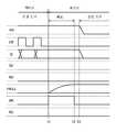
도 6 및 도 7은 SFF(110)의 동작예를 각각 도시한 타이밍 차트이다. 도 6은 SFF(110)를 포함하는 반도체 장치가 액티브 모드에서 슬리프 모드로 이행될 때의 SFF(110)의 동작예를 도시한 것이다. 도 7은 상기 반도체 장치가 슬리프 모드에서 액티브 모드로 이행될 때의 SFF(110)의 동작예를 도시한 것이다. 도 6 및 도 7은 단자(VH, CK, Q, SE, SD, BK, 및 RE) 및 노드(FN11)의 전압(논리)의 변화를 도시한 것이다. 도 6 및 도 7에서 최대 전압은 VDD이고 최소 전압은 VSS이다. 또한 t1 내지 t10은 각각 시간을 가리킨다.6 and 7 are timing charts each showing an operation example of the SFF 110 . 6 illustrates an operation example of the SFF 110 when the semiconductor device including the SFF 110 transitions from the active mode to the sleep mode. 7 illustrates an operation example of the SFF 110 when the semiconductor device transitions from the sleep mode to the active mode. 6 and 7 show changes in voltage (logic) of the terminals VH, CK, Q, SE, SD, BK, and RE and the node FN11. 6 and 7 , the maximum voltage is VDD and the minimum voltage is VSS. In addition, t1 to t10 indicate time, respectively.
<액티브 모드(통상 동작 모드)><Active mode (normal operation mode)>
액티브 모드에서 SFF(110)는 통상 동작을 수행한다. SFF(110)는 논리 회로로부터의 출력 데이터를 일시적으로 유지하는 플립플롭으로서 기능한다. 여기서, 논리 회로로부터 출력되는 데이터는 단자(D)에 입력된다. 통상 동작에서는 RE 및 BK가 "L"이고, 트랜지스터(M1 내지 M3)는 오프 상태이다. SE는 "L"이고, SEL(21)에 의하여 단자(D)는 FF(31)의 입력 단자에 접속된다. RT는 "H"이다. 신호(CLK)는 CK에 입력된다. CK가 "H"로 변화되는 것과 연동하여 Q의 전압(논리)이 변화된다.In the active mode, the SFF 110 performs a normal operation. The SFF 110 functions as a flip-flop that temporarily holds the output data from the logic circuit. Here, the data output from the logic circuit is inputted to the terminal (D). In normal operation, RE and BK are "L", and the transistors M1 to M3 are off. SE is "L", and the terminal D is connected to the input terminal of the
<스캔 모드><Scan Mode>
스캔 모드에서는, 복수의 SFF(110)가 직렬로 전기적으로 접속되어 스캔 체인을 형성한다. 회로(RC11)에서는, 트랜지스터(M1 및 M2)가 온 상태가 되고 트랜지스터(M3)가 오프 상태가 된다. SE가 "H"이기 때문에, SEL(21)에 의하여 SD는 FF(31)의 입력 단자에 전기적으로 접속된다. 바꿔 말하면, 스캔 모드에서는 SFF(11)의 Q로부터 출력되는 데이터가 다음 스테이지의 SFF(11)의 SD에 입력된다.In the scan mode, a plurality of SFFs 110 are electrically connected in series to form a scan chain. In the circuit RC11, the transistors M1 and M2 are turned on and the transistor M3 is turned off. Since SE is "H", SD is electrically connected to the input terminal of FF (31) by SEL (21). In other words, in the scan mode, data output from the Q of the
(스캔 테스트)(Scan test)
스캔 테스트를 수행하기 위해서는, 모드를 스캔 모드로 하고, 스캔 체인의 제 1 스테이지의 SFF(110)의 SD_IN에 스캔 테스트 데이터(SCNIN)를 입력한다. CLK의 입력에 의하여 스캔 체인의 시프트 동작을 수행하고, 스캔 체인의 SFF(110)에 스캔 테스트 데이터(SCNIN)를 기록한다. 다음에, SFF(110)는 통상 동작을 수행하여 SFF(110)의 논리 회로로부터 출력되는 데이터를 유지한다. 모드를 다시 스캔 모드로 하여 스캔 체인의 시프트 동작을 수행한다. 마지막 스테이지의 SFF(110)의 Q로부터 출력되는 데이터로부터, 논리 회로 및 SFF(110)에 고장이 난지 여부를 판정할 수 있다.In order to perform the scan test, the mode is set to the scan mode, and the scan test data SCNIN is input to SD_IN of the SFF 110 of the first stage of the scan chain. A shift operation of the scan chain is performed according to the input of CLK, and scan test data SCNIN is recorded in the SFF 110 of the scan chain. Next, the SFF 110 maintains data output from the logic circuit of the SFF 110 by performing a normal operation. The shift operation of the scan chain is performed by changing the mode back to the scan mode. From the data output from Q of the SFF 110 of the last stage, it may be determined whether a failure occurs in the logic circuit and the SFF 110 .
(백업 시퀀스)(backup sequence)
액티브 모드에서 슬리프 모드로의 이행에 의하여 백업 시퀀스가 수행된다. 백업 시퀀스에서는, 클록 게이팅(클록 정지), 데이터 백업, 및 파워 게이팅(전원 오프)이 수행된다. 클록의 공급을 정지함으로써 모드를 슬리프 모드로 한다.A backup sequence is performed by transitioning from the active mode to the sleep mode. In the backup sequence, clock gating (clock stop), data backup, and power gating (power off) are performed. The mode is set to sleep mode by stopping the clock supply.
도 6의 예에서는, t1에서 SFF(11)의 클록 게이팅이 시작하고, 회로(RC11)에서 백업 동작이 시작한다. 구체적으로는, t1에서 CK를 "L"로 하고 BK를 "H"로 한다. BK가 "H"인 기간이 백업 동작 기간이다. BK를 "H"로 하면 트랜지스터(M2)는 FN11과 Q를 전기적으로 접속시킨다. 이로써, Q가 "0"일 때 FN11은 "L"을 유지하고, Q가 "1"일 때 FN11의 전압은 "H"로 상승된다. 바꿔 말하면, BK가 "H"인 기간에는 FN11의 논리를 Q의 논리와 같게 할 수 있다. FN11의 전압을 "1" 논리 레벨까지 상승할 수 있도록, BK가 "H"인 기간을 결정하면 좋다. t2에서, BK를 "L"로 하여 트랜지스터(M1 및 M2)를 오프 상태로 함으로써, FN11은 전기적으로 부유 상태가 되어 회로(RC11)는 데이터를 유지한다.In the example of Fig. 6, clock gating of the
t3에서 전원을 차단하여 RT를 "L"로 한다. VH의 전압은 VDD로부터 VSS로 서서히 저하된다. t2에서 전원을 차단하여도 좋다. 또한, 필요에 따라 전원을 차단하여도 좋다. SFF(110)를 포함하는 반도체 장치의 파워 도메인 또는 슬리프 모드 시간 등에 따라, 슬리프 모드에서 액티브 모드로 복귀하는 데 요구된 전력이, 전원 오프에 의하여 저감될 수 있는 전력보다 높아질 가능성이 있다. 이 경우에는 파워 게이팅의 효과를 얻을 수 없기 때문에, 슬리프 모드에서는 전원을 차단하지 않고 클록 공급만을 정지하는 것이 바람직하다.Turn off the power at t3 to set RT to “L”. The voltage on VH gradually drops from VDD to VSS. The power may be cut off at t2. Moreover, you may cut off the power supply as needed. Depending on the power domain or sleep mode time of the semiconductor device including the SFF 110 , the power required to return to the active mode from the sleep mode may be higher than the power that can be reduced by turning off the power. In this case, since the effect of power gating cannot be obtained, it is preferable to stop only the clock supply without shutting off the power in the sleep mode.
(복원 시퀀스)(restore sequence)
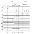
모드가 슬리프 모드에서 액티브 모드로 이행되는 복원 시퀀스에서는, 전원이 온되고, 데이터가 복원되며, 클록이 공급된다. 모드는 클록 공급을 시작함으로써 액티브 모드로 이행된다.In the recovery sequence in which the mode is transitioned from the sleep mode to the active mode, power is turned on, data is restored, and a clock is supplied. The mode is transitioned to active mode by starting the clock supply.
t4에서 전원을 온한다. VH의 전압이 VSS로부터 VDD로 서서히 상승된다. VH가 VDD로 된 후에 복원 동작이 시작한다. t5에서 SE 및 RE를 "H"로 한다. 또한 RT를 "H"로 한다. RE가 "H"인 동안 복원 동작이 수행된다. 트랜지스터(M3)가 온 상태가 되어 FN11은 SD에 접속된다. FN11이 "L"일 때 SD는 "L"을 유지한다. FN11이 "H"일 때 SD의 전압은 "H"로 상승된다. t6에서 SE를 "H"로 한다. SE 및 SEL(21)에 의하여 SD는 FF(31)의 입력 단자에 전기적으로 접속된다. 바꿔 말하면, RE를 "H"로 하면, FN11에 유지된 데이터가 SD에 기록된다.Turn on the power at t4. The voltage on VH rises slowly from VSS to VDD. After VH becomes VDD, the restoration operation starts. Let SE and RE be "H" at t5. In addition, let RT be "H". A restoration operation is performed while RE is "H". Transistor M3 is turned on, and FN11 is connected to SD. SD holds "L" when FN11 is "L". When FN11 is "H", the voltage of SD is raised to "H". Let SE be "H" at t6. SD is electrically connected to the input terminal of FF (31) by SE and SEL (21). In other words, when RE is "H", data held in FN11 is written to SD.
또한 t5에서 RE와 함께 SE도 "H"로 할 수 있다. 도 7에 도시된 바와 같이, FN11이 "H"인 경우, SD의 전압이 "1" 논리 레벨까지 상승된 후에 SE를 "H"로 하는 것이 바람직하다. 이 구동은 SFF(11)를 통하여 관통 전류가 흐르는 것을 방지한다.In addition, at t5, SE together with RE may be set to "H". As shown in Fig. 7, when FN11 is "H", it is preferable to set SE to "H" after the voltage of SD rises to "1" logic level. This drive prevents a through current from flowing through the
용량 분배에 의하여 FN11의 데이터를 SD에 기록하기 위하여 FN11이 "H"인 동안 FN11이 SD에 접속되는 경우, SD의 기생 용량에 의하여 FN11의 전압이 저하된다. 따라서, C11의 용량은 SD의 기생 용량보다 충분히 클 필요가 있다. C11의 용량은, SD의 데이터가 입력되는 논리 회로의 특성 등을 고려하여 결정한다. 예를 들어, 이 논리 회로의 문턱 전압이 VDD/2인 경우, C11의 용량은 SD의 기생 용량 이상일 필요가 있다.When FN11 is connected to SD while FN11 is "H" in order to write data of FN11 to SD by capacity distribution, the voltage of FN11 is lowered by the parasitic capacitance of SD. Therefore, the capacity of C11 needs to be sufficiently larger than the parasitic capacity of SD. The capacity of C11 is determined in consideration of characteristics of a logic circuit to which SD data is input, and the like. For example, when the threshold voltage of this logic circuit is VDD/2, the capacitance of C11 needs to be greater than or equal to the parasitic capacitance of SD.
SD의 논리가 FN11의 논리와 같아진 후, 일정 기간(t7부터 t8까지) CK는 "H"이다. 도 7의 예에서는 1클록의 CLK가 CK에 입력된다. t7에서 CK를 "H"로 하면 래치(32M)의 데이터가 래치(32S)에 기록된다. t7에서 SD가 "0"일 때 Q는 "0"이 되고, SD가 "1"일 때 Q는 "1"이 된다. 바꿔 말하면, FN11의 데이터가 Q에 기록되고, SFF(110)는 CLK의 공급이 정지되기(즉, 모드가 슬리프 모드로 되기) 직전의 상태로 되돌아간다. t9에서 SE 및 RE를 "L"로 함으로써 복원 동작이 종료된다. SEL(21)에 의하여 D는 FF(31)의 입력 단자에 전기적으로 접속된다. 회로(RC11)에서는, 트랜지스터(M3)가 오프 상태가 되어 노드(FN11)가 부유 상태가 된다.After the logic of SD becomes the same as that of FN11, CK is "H" for a certain period (from t7 to t8). In the example of Fig. 7, CLK of one clock is input to CK. When CK is set to "H" at t7, the data of the
SE 및 RE를 "L"로 한 후, 일정 기간(예를 들어 1클록 기간) 경과 후에 t10에서 CLK의 입력을 재개하여 SFF(110)를 액티브 모드로 한다. SFF(110)는 통상 동작을 수행한다.After setting SE and RE to "L", CLK input is resumed at t10 after a certain period (eg, one clock period) has elapsed to put the SFF 110 in the active mode. The SFF 110 performs a normal operation.
상술한 바와 같이, SFF(110)는 고속으로 백업 및 복원을 수행할 수 있고, 예를 들어, 몇 클록(2클록 내지 5클록) 이내로 백업 동작 및 복원 동작을 완료할 수 있다. 회로(RC11)의 기록 동작에서는 트랜지스터(M1 내지 M3)의 동작을 전환함으로써 FN11이 충전 또는 방전된다. 회로(RC11)의 판독 동작에서는 트랜지스터(M1 내지 M3)의 동작을 전환함으로써 SD가 충전 또는 방전된다. 이들 동작에 필요한 에너지는 DRAM 셀에 필요한 에너지만큼 낮다. 데이터 유지를 위하여 회로(RC1)에 전원을 공급할 필요가 없기 때문에, SFF(110)의 대기 전력을 저감시킬 수 있다. 마찬가지로, 통상 동작에서 회로(RC11)에 전원을 공급할 필요가 없기 때문에, 회로(RC11)는 SFF(110)의 다이내믹 전력의 실질적인 증가로 이어지지 않는다. 회로(RC11)는 트랜지스터(M1)의 기생 용량을 단자(Q)에 부가시킨다. 그러나, 이 기생 용량은 단자(Q)에 접속되는 논리 회로의 기생 용량보다 낮다. 결과적으로, SFF(110)의 통상 동작은 영향을 받지 않고, 회로(RC11)는 액티브 모드에서 SFF(110)의 실질적인 성능 저하로 이어지지 않는다.As described above, the SFF 110 may perform backup and restoration at high speed, and, for example, may complete the backup operation and restoration operation within several clocks (2 clocks to 5 clocks). In the write operation of the circuit RC11, FN11 is charged or discharged by switching the operations of the transistors M1 to M3. In the read operation of the circuit RC11, the SD is charged or discharged by switching the operations of the transistors M1 to M3. The energy required for these operations is as low as the energy required for a DRAM cell. Since it is not necessary to supply power to the circuit RC1 for data retention, the standby power of the SFF 110 can be reduced. Likewise, since it is not necessary to supply power to the circuit RC11 in normal operation, the circuit RC11 does not lead to a substantial increase in the dynamic power of the SFF 110 . Circuit RC11 adds the parasitic capacitance of transistor M1 to terminal Q. However, this parasitic capacitance is lower than the parasitic capacitance of the logic circuit connected to the terminal Q. As a result, the normal operation of the SFF 110 is not affected, and the circuit RC11 does not lead to substantial performance degradation of the SFF 110 in the active mode.
스캔 FF를 예로 들어 유지 회로의 다른 회로 구조예에 대하여 이하에서 설명한다.Taking the scan FF as an example, another example of the circuit structure of the holding circuit will be described below.
<유지 회로의 구조예 2><Structural example 2 of holding circuit>
도 8의 SFF(112)는 회로(RC12) 및 SFF(11)를 포함한다. 회로(RC12)는 회로(RC11)(도 4)의 변형예이고, 노드(FN11)와 단자(RE) 사이의 용량 결합을 위한 용량 소자(C12)를 포함한다. 이러한 회로 구조에 의하여, 복원 동작에서 RE의 전압을 VDD("H")로 하는 경우, 노드(FN11)의 전압을 상승시킬 수 있다. 따라서, 회로(RC12)는 회로(RC11)보다 길게 "H" 전압을 유지할 수 있다. 그러나, 이 경우, 노드(FN11)가 "L" 전압을 유지할 때도 노드(FN11)의 전압이 상승된다. 따라서, 이 경우, 노드(FN11)의 "L" 전압이 SD에 기록될 때, SD의 전압이 "0" 논리 레벨을 갖도록 용량 소자(C12)의 용량을 설정한다. 그 결과, 용량 소자(C12)의 용량은 C11의 용량보다 낮다.The SFF 112 of FIG. 8 includes a circuit RC12 and an
<유지 회로의 구조예 3 및 4><Structural examples 3 and 4 of holding circuit>
도 9의 SFF(113)는 회로(RC13) 및 SFF(11)를 포함한다. 도 10의 SFF(114)는 회로(RC14) 및 SFF(11)를 포함한다.The SFF 113 of FIG. 9 includes a circuit RC13 and an
도 8의 회로(RC12)에서는, 노드(FN11)의 "H" 전압을 노드(SD)에 기록할 때, 용량 소자(C11)에 대한 용량 소자(C12)의 용량비에 따라 SD의 전압은 "1" 논리 레벨을 초과할 경우가 있다. 이러한 경우, 회로(RC13) 또는 회로(RC14)를 유지 회로로서 사용하면 좋다. 회로(RC13)는 회로(RC12)에 버퍼(45)(이하에서는 BUF(45)라고 함)를 추가하여 얻어진 회로이다. BUF(45)의 입력 단자는 트랜지스터(M3)의 드레인(소스)에 전기적으로 접속된다. BUF(45)의 출력 단자는 SD에 전기적으로 접속된다. BUF(45)의 트랜지스터는 VDD를 초과하는 게이트 전압을 견딜 수 있는 것이 바람직하다.In the circuit RC12 of Fig. 8, when the voltage "H" of the node FN11 is written to the node SD, the voltage of SD is "1" according to the capacitance ratio of the capacitor C12 to the capacitor C11. "There are cases where the logic level is exceeded. In this case, the circuit RC13 or the circuit RC14 may be used as the holding circuit. The circuit RC13 is a circuit obtained by adding a buffer 45 (hereinafter referred to as a BUF 45) to the circuit RC12. The input terminal of the
도 10의 회로(RC14)는 회로(RC13)의 변형예이다. 도 10에 도시된 바와 같이 용량 소자(C12)의 접속이 변경되었다. 용량 소자(C12)의 한쪽 단자는 트랜지스터(M3)의 드레인(소스)에 전기적으로 접속된다. 용량 소자(C12)의 다른 쪽 단자는 BUF(45)의 입력 단자에 전기적으로 접속된다. BUF(45)는 필요에 따라 회로(RC14)에 제공된다.The circuit RC14 in FIG. 10 is a modified example of the circuit RC13. As shown in Fig. 10, the connection of the capacitive element C12 has been changed. One terminal of the capacitor C12 is electrically connected to the drain (source) of the transistor M3. The other terminal of the capacitive element C12 is electrically connected to the input terminal of the
<유지 회로의 구조예 5 및 6><Structural examples 5 and 6 of holding circuit>
도 11의 SFF(115)는 회로(RC15) 및 SFF(11)를 포함한다. 도 12의 SFF(116)는 회로(RC16) 및 SFF(11)를 포함한다. 회로(RC15) 및 회로(RC16)는 회로(RC11)의 변형예이고, 백 게이트를 갖는 트랜지스터(M1 내지 M3)를 포함한다.The SFF 115 of FIG. 11 includes a circuit RC15 and an
회로(RC15)에서, 트랜지스터(M1 내지 M3)의 백 게이트는 단자(OBG)에 전기적으로 접속된다. OBG에는 신호 또는 고정 전위가 입력될 수 있다. 또는 OBG에는 용량 소자가 접속되어도 좋다. 이 용량 소자는 트랜지스터(M1 내지 M3)의 백 게이트의 전압이 유지될 수 있도록 충전되어도 좋다. 예를 들어, 트랜지스터(M1 내지 M3)의 문턱 전압을 트랜지스터(M1 내지 M3)의 백 게이트의 전압에 따라 조절할 수 있다.In the circuit RC15, the back gates of the transistors M1 to M3 are electrically connected to the terminal OBG. A signal or a fixed potential may be input to the OBG. Alternatively, a capacitor may be connected to the OBG. This capacitor may be charged so that the voltage of the back gates of the transistors M1 to M3 can be maintained. For example, the threshold voltages of the transistors M1 to M3 may be adjusted according to the voltages of the back gates of the transistors M1 to M3 .
회로(RC16)에서는, 트랜지스터(M1 내지 M3)의 게이트에 백 게이트가 전기적으로 접속된다. 이러한 디바이스 구조에 의하여 트랜지스터(M1 내지 M3)의 온 전류 특성을 향상시킬 수 있다.In the circuit RC16, a back gate is electrically connected to the gates of the transistors M1 to M3. With this device structure, the on-current characteristics of the transistors M1 to M3 may be improved.
트랜지스터(RC15)에서는, 트랜지스터(M1 내지 M3)가 백 게이트를 포함하지만, 트랜지스터(M1 내지 M3) 중 일부의 트랜지스터는 백 게이트를 포함하지 않아도 된다. 트랜지스터(M1)가 백 게이트를 포함하는 경우, 이 백 게이트는 단자(OBG)에 접속되어도 좋고, 트랜지스터(M1)의 게이트에 전기적으로 접속되어도 좋다. 트랜지스터(M2 및 M3)에 대해서도 마찬가지이다. 또한 회로(RC16)에 대해서도 마찬가지이다.In the transistor RC15, the transistors M1 to M3 include a back gate, but some of the transistors M1 to M3 need not include a back gate. When the transistor M1 includes a back gate, the back gate may be connected to the terminal OBG or electrically connected to the gate of the transistor M1. The same is true for transistors M2 and M3. The same applies to the circuit RC16.
<처리 유닛의 구조예><Structural example of processing unit>
스캔 FF를 포함하는 반도체 장치의 예에 대하여 설명한다. 도 13의 반도체 장치는 처리 유닛(PU)(200) 및 전원 회로(210)를 포함한다. PU(200)는 명령을 실행하는 기능을 갖는다. PU(200)는 하나의 칩 위에 집적된 복수의 기능 회로를 포함한다. PU(200)는 프로세서 코어(201), 전원 관리 유닛(PMU)(202), 파워 스위치(PSW)(203), 및 클록 제어 회로(204)를 더 포함한다. 도 13은, PU(200)가 제공된 칩과 다른 칩 위에 전원 회로(210)가 제공되는 예를 도시한 것이다. 단자(220)는 전원 단자이고, 단자(220)에는 전원 전압(VDD)이 전원 회로(210)로부터 입력된다. 단자(221 및 222)는 신호 입력 단자이다. 단자(221)에는 마스터 클록 신호(MCLK)가 입력된다. 단자(222)에는 신호(INT)가 입력된다. 신호(INT)는 인터럽트 처리를 요구하기 위한 인터럽트 신호이다. 신호(INT)는 프로세서 코어(201) 및 PMU(202)에 입력된다.An example of a semiconductor device including the scan FF will be described. The semiconductor device of FIG. 13 includes a processing unit (PU) 200 and a
<프로세서 코어><processor core>
프로세서 코어(201)는 명령을 실행할 수 있고, 연산 처리 회로 또는 프로세서(처리 유닛)라고도 불릴 수 있다. 프로세서 코어(201)는 논리 회로(240) 및 스캔 FF(SFF)(250) 등을 포함하고, 이들 회로를 사용하여 다양한 기능 회로가 형성된다. 예를 들어, 논리 회로(240)는 조합 회로로 할 수 있다. 예를 들어, SFF(250)는 레지스터에 포함된다. SFF(250)는 SFF(50) 및 회로(RC50)를 포함한다. SFF(50)는 스캔 FF로서 기능하면 좋고, 표준적인 회로 라이브러리에 준비되는 스캔 FF를 사용하여 형성할 수 있다. 회로(RC50)는 SFF(50)의 백업 유지 회로이고, 회로(RC11 내지 RC14) 중 어느 것을 회로(RC50)로서 사용할 수 있다. SFF(250)의 단자(Q)는 논리 회로(240)의 입력 단자에 전기적으로 접속되고, 스캔 체인을 형성하기 위하여 다른 SFF(250)의 단자(SD_IN)에도 전기적으로 접속된다. SFF(250)는 프로세서 코어(201)의 클록 게이팅 및 파워 게이팅이 가능하기 때문에, PU(200)의 소비전력을 저감시킬 수 있다.The
도 14는 프로세서 코어(201)의 구조예를 도시한 것이다. 도 14의 프로세서 코어(201)는 제어 유닛(231), 프로그램 카운터(232), 파이프라인 레지스터(233), 파이프라인 레지스터(234), 레지스터 파일(235), 연산 논리 유닛(ALU)(236), 및 데이터 버스(237)를 포함한다. 데이터는 데이터 버스(237)를 통하여 프로세서 코어(201)와 PMU(202) 또는 캐시 등의 주변 회로 사이에서 전달된다.14 shows a structural example of the
제어 유닛(231)은 프로그램 카운터(232), 파이프라인 레지스터(233), 파이프라인 레지스터(234), 레지스터 파일(235), ALU(236), 및 데이터 버스(237)의 종합적인 동작을 제어함으로써, 입력된 애플리케이션 등의 프로그램에 포함되는 명령을 디코딩하여 실행하는 기능을 갖는다. ALU(236)는 사칙 연산 및 논리 연산 등의 각종 연산 처리를 수행하는 기능을 갖는다. 프로그램 카운터(232)는 다음에 실행되는 명령의 어드레스를 저장하는 기능을 갖는 레지스터이다.The
파이프라인 레지스터(233)는 명령 데이터를 일시적으로 저장하는 기능을 갖는다. 레지스터 파일(235)은 범용 레지스터를 포함하는 복수의 레지스터를 포함하고, 메인 메모리로부터 판독되는 데이터, 또는 ALU(236)에서의 연산 처리의 결과로서 얻어진 데이터 등을 저장할 수 있다. 파이프라인 레지스터(234)는 ALU(236)에서 수행되는 연산 처리에 사용되는 데이터, 또는 ALU(236)에서의 연산 처리의 결과로서 얻어진 데이터 등을 일시적으로 저장하는 기능을 갖는다.The pipeline register 233 has a function of temporarily storing instruction data. The
<전원 관리><Power Management>
PMU(202)는 파워 게이팅 및 클록 게이팅 등을 제어하는 기능을 갖는다. 구체적으로, PMU(202)는 프로세서 코어(201), PSW(203), 및 클록 제어 회로(204)를 제어할 수 있다. PMU(202)는 BKsig, REsig, 및 SEsig 등의 제어 신호를 프로세서 코어(201)에 출력하는 기능을 갖는다.The
PMU(202)는 회로(205)를 포함한다. 회로(205)는 시간을 측정할 수 있다. PMU(202)는 회로(205)에 의하여 얻어지는 시간에 관한 데이터에 기초하여 전원 관리를 수행할 수 있다. 예를 들어, 회로(205)가 타이머 회로일 때, PMU(202)는 타이머 인터럽트 요구 신호를 생성하여도 좋다. 회로(205)는 필요에 따라 제공된다.
PSW(203)는 PMU(202)의 제어 신호에 따라 PU(200)로의 VDD 공급을 제어할 수 있다. 도 13의 예에서, 프로세서 코어(201)는 복수의 파워 도메인을 포함하여도 좋다. 이 경우, 복수의 파워 도메인으로의 전원 공급은 PSW(203)에 의하여 독립적으로 제어되어도 좋다. 또한, 프로세서 코어(201)는 파워 게이팅되지 않는 파워 도메인을 포함하여도 좋다. 이 경우, PSW(203)를 통하지 않고 이 파워 도메인에 VDD가 공급되어도 좋다.The
클록 제어 회로(204)는 신호(MCLK)로부터 게이티드 클록 신호(gated clock signal)를 생성하여 출력하는 기능을 갖는다. 클록 제어 회로(204)는 PMU(202)의 제어 신호에 따라 프로세서 코어(201)로의 클록 신호 공급을 정지할 수 있다. 전원 회로(210)는 PMU(202)의 제어 신호에 따라 VDD의 크기를 변경할 수 있어도 좋다.The
프로세서 코어(201)로부터 PMU(202)에 신호(SLP)가 출력된다. 신호(SLP)는 프로세서 코어(201)를 슬리프 모드로 이행시키기 위한 트리거 신호이다. 프로세서 코어(201)에서는 SFF(250)의 백업 시퀀스가 신호(SLP)에 따라 실행된다. SFF(250)의 백업 시퀀스는 도 6의 SFF(110)의 백업 시퀀스와 같은 식으로 실행될 수 있다. PMU(202)에 신호(SLP)가 입력되면, PMU(202)는 액티브 모드에서 슬리프 모드로의 이행을 위한 제어 신호를 제어 대상의 기능 회로에 출력한다. PMU(202)는 클록 제어 회로(204)를 제어하여 프로세서 코어(201)로의 클록 신호 공급을 정지한다. 또한, PMU(202)는 PSW(203)를 제어하여 프로세서 코어(201)로의 전원 공급을 정지한다.A signal SLP is output from the
프로세서 코어(201)를 슬리프 모드에서 액티브 모드로 복원하기 위한 처리는 신호(INT)의 입력에 의하여 실행된다. 프로세서 코어(201)에서 SFF(250)의 복원 시퀀스는 신호(INT)에 따라 실행된다. SFF(250)의 복원 시퀀스는 도 7의 SFF(110)의 복원 시퀀스와 같은 식으로 수행될 수 있다. PMU(202)에 신호(INT)가 입력되면, PMU(202)는 슬리프 모드에서 액티브 모드로의 이행을 위한 제어 신호를 제어 대상의 기능 회로에 출력한다. PMU(202)는 PSW(203)를 제어하여 프로세서 코어(201)로의 전원 공급을 재개한다. 또한, PMU(202)는 클록 제어 회로(204)를 제어하여 프로세서 코어(201)로의 클록 신호 공급을 재개한다.The processing for restoring the
백업 시퀀스는 신호(INT) 또는 PMU(202)의 인터럽트 요구 신호를 트리거로서 사용하여 실행되어도 좋다. 또한 복원 시퀀스는 PMU(202)의 인터럽트 요구 신호를 트리거로서 사용하여 실행되어도 좋다.The backup sequence may be executed using the signal INT or the interrupt request signal of the
<SFF(250)의 디바이스 구조><Device structure of SFF 250>
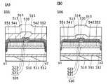
도 15는 SFF(250)의 디바이스 구조를 도시한 것이다. 도 15에서, 회로(RC50)는 회로(RC11)(도 4)와 같은 회로 구조를 갖는다. 트랜지스터(M1 내지 M3)는 OS 트랜지스터이다. SFF(250)는, 회로(RC50)가 SFF(50) 위에 적층된 3D 디바이스 구조를 가질 수 있다. 제 1 배선층, 제k 배선층, 제 (k+1) 배선층, 및 제h 배선층은 각각 W1, Wk, Wk+1, 및 Wh로 나타낸다. 여기서,k는 1 이상의 정수이고h는 (k+2) 이상의 정수이다. SFF(50)의 단자(D, SD, Q, SE, 및 CK)는 배선층(Wk)에 제공되고, 회로(RC50)의 단자(SD_IN)는 배선층(Wh)에 제공된다.15 shows a device structure of the SFF 250 . In Fig. 15, circuit RC50 has the same circuit structure as circuit RC11 (Fig. 4). Transistors M1 to M3 are OS transistors. The SFF 250 may have a 3D device structure in which the circuit RC50 is stacked on the SFF 50 . The first wiring layer, thekth wiring layer, the (k +1)th wiring layer, and thehth wiring layer are denoted by W1 , Wk , Wk+1 , and Wh , respectively. Here,k is an integer greater than or equal to 1 andh is aninteger greater than or equal to (k +2). The terminals D, SD, Q, SE, and CK of the SFF 50are provided to the wiring layer W k , and the terminal SD_IN of the circuit RC50 is provided to thewiring layer W h .
SFF(50)의 트랜지스터는 FET층(260)에 제공된다. FET층(260)의 트랜지스터는 표준적인 CMOS 프로세스에 의하여 형성하면 좋다. 배선층(W1 내지 Wk)의 도전체는 FET층(260)의 트랜지스터들을 서로 전기적으로 접속시킨다. 배선층(Wk+1 내지 Wh)의 도전체는 SFF(50)와 회로(RC50)를 전기적으로 접속시킨다.The transistor of the SFF 50 is provided in the
회로(RC50)에서의 소자의 수는 SFF(50)에서의 소자의 수보다 대폭으로 적기 때문에, 회로(RC50)를 적층시키기 위하여 SFF(50)의 회로 구조 및 레이아웃을 바꿀 필요는 없다. 바꿔 말하면, 회로(RC50)는 매우 넓은 유용성을 갖는 백업 회로이다. 또한 회로(RC50)는 SFF(50)가 형성된 영역에 제공할 수 있기 때문에, 회로(RC50)가 포함되더라도, SFF(250)의 면적 오버헤드는 제로이다.Since the number of elements in the circuit RC50 is significantly smaller than the number of elements in the SFF 50, it is not necessary to change the circuit structure and layout of the SFF 50 in order to stack the circuits RC50. In other words, circuit RC50 is a backup circuit with very wide utility. Also, since the circuit RC50 can be provided in the region where the SFF 50 is formed, even if the circuit RC50 is included, the area overhead of the SFF 250 is zero.
<회로(RC50)를 포함하는 집적 회로><Integrated circuit including circuit RC50>
도 13의 프로세서 코어(201)에서 회로(RC50)는 SFF(50)의 배치에 영향을 주지 않고, 스캔 테스트를 효율적으로 실시할 수 있도록 SFF(50)를 배치할 수 있다. 바꿔 말하면, 회로(RC50)를 백업 회로로서 사용하면, 백업 기능을 갖는 집적 회로를 쉽게 설계할 수 있고 테스트의 용이성도 확보할 수 있다.In the
프로세서 코어(201)에서는, SFF(50)에서와 같이, NAND 회로 등의 다른 표준 셀이 FET층(260) 및 배선층(W1 내지 Wk)에 제공된다. 회로(RC50)와 단자(SD 및 Q)를 접속시키기 위한 도전체는 배선층(W1 내지 Wk)에 형성되기 때문에, 이들 도전체 주위의 배선을 우회하여 다른 표준 셀의 배선을 레이아웃할 필요가 있다. 따라서, 프로세서 코어(201)의 면적이 증가되는 경우가 있다. SFF(250)는 프로세서 코어(201)에 많이 포함되는 표준 셀의 한 가지이지만, 회로(RC50)로 인한 SFF(250)의 면적 오버헤드는 제로이다. 따라서, 프로세서 코어(201)의 면적 증가는 다른 표준 셀들 간의 배선 레이아웃의 변경으로 인한 것이고, 프로세서 코어(201)의 면적 오버헤드는 수% 미만으로 할 수 있다. 이 사실은 회로(RC50)를 포함하는 프로세서 코어를 설계함으로써 확인된다. 시뮬레이션은 회로(RC50)를 포함하는 프로세서 코어의 소비전력이 저감될 수 있는 것을 가리킨다.In the
<프로세서 코어의 면적 및 전력><Area and Power of Processor Core>
회로(RC50)를 포함하는 스캔 FF를 포함하는 프로세서 코어를 설계한다. 이 프로세서 코어를 OS-FF 탑재 프로세서라고 부르고, 회로(RC50)를 포함하는 스캔 FF를 OS-FF라고 부른다. 비교를 위하여, 회로(RC50)를 포함하지 않은 스캔 FF를 포함하는 CPU 코어를 설계한다. 이 프로세서 코어를 Si-FF 탑재 프로세서라고 부른다.Design a processor core including scan FF including circuit RC50. This processor core is called an OS-FF mounted processor, and the scan FF including the circuit RC50 is called OS-FF. For comparison, a CPU core including a scan FF that does not include the circuit RC50 is designed. This processor core is called Si-FF-equipped processor.
설계한 프로세서 코어는 RISC 프로세서 코어이다. OS-FF 탑재 프로세서 및 Si-FF 탑재 프로세서는 회로(RC50) 유무 이외는 같은 회로 구조를 갖는다. 회로(RC50) 이외의 회로는 Si 트랜지스터를 사용하여 형성된다. 프로세서 코어는 Si 트랜지스터의 채널 길이가 60nm이고 OS 트랜지스터의 채널 길이가 60nm인 디자인 룰에 의하여 설계한다. Si-FF 탑재 프로세서의 면적은 275μm×272μm로 하고 OS-FF 탑재 프로세서의 면적은 275μm×272μm로 한다. 스캔 FF는 프로세서 코어의 논리 회로의 약 절반을 차지한다. OS-FF 탑재 프로세서의 각 스캔 FF가 회로(RC50)를 포함하더라도, 면적 오버헤드는 3%로 작다.The designed processor core is a RISC processor core. The OS-FF-mounted processor and the Si-FF-mounted processor have the same circuit structure except for the presence or absence of the circuit RC50. Circuits other than the circuit RC50 are formed using Si transistors. The processor core is designed according to the design rule that the channel length of the Si transistor is 60 nm and the channel length of the OS transistor is 60 nm. The area of the Si-FF-equipped processor is 275 μm×272 μm, and the area of the OS-FF-mounted processor is 275 μm×272 μm. The scan FF occupies about half of the logic circuitry of the processor core. Even if each scan FF of the OS-FF mounted processor includes the circuit RC50, the area overhead is as small as 3%.
시뮬레이션은 전원 전압 1.2V일 때의 Si-FF 탑재 프로세서의 다이내믹 전력이 19μA/MHz이고, OS-FF 탑재 프로세서의 다이내믹 전력도 19μA/MHz이고, 회로(RC50)의 추가로 인하여 다이내믹 전력이 증가되지 않는 것을 가리킨다. 또한, 파워 게이팅을 수행할 때의 OS-FF 탑재 프로세서의 대기 전력은 0.03μA로 추정된다.The simulation shows that the dynamic power of the processor equipped with Si-FF is 19 μA/MHz when the power supply voltage is 1.2 V, the dynamic power of the processor equipped with OS-FF is also 19 μA/MHz, and the dynamic power is not increased due to the addition of the circuit (RC50). refers to not In addition, the standby power of the OS-FF-equipped processor when power gating is performed is estimated to be 0.03 μA.
설계한 OS-FF의 성능을 시뮬레이션을 통하여 증명한다. OS 트랜지스터의 채널 길이가 65nm이고 OS 트랜지스터의 문턱 전압이 1.6V인 경우, 실온에서의 OS-FF의 유지 시간은 30일간을 넘는다. 바꿔 말하면, OS-FF 탑재 프로세서의 슬리프 기간에서, OS-FF는 비휘발성 저장 회로로서 충분한 유지 성능을 갖는다.The performance of the designed OS-FF is verified through simulation. When the channel length of the OS transistor is 65 nm and the threshold voltage of the OS transistor is 1.6 V, the OS-FF retention time at room temperature exceeds 30 days. In other words, in the sleep period of the OS-FF-equipped processor, the OS-FF has sufficient holding performance as a non-volatile storage circuit.
시뮬레이션에서는, 동작 주파수가 50MHz일 때의 OS-FF의 백업 시간 및 복원 시간은 각각 2클록이다. 파워 게이팅 동작으로 인한 OS-FF 탑재 프로세서의 오버헤드 시간은 충분히 짧으므로, OS-FF는 프로세서의 성능을 저하시키지 않는다.In the simulation, the backup time and restoration time of OS-FF when the operating frequency is 50 MHz are 2 clocks each. Since the overhead time of the OS-FF-equipped processor due to the power gating operation is sufficiently short, OS-FF does not degrade the performance of the processor.
파워 게이팅에 의하여 발생하는 OS-FF 탑재 프로세서의 전력 저감 효과를 시뮬레이션을 통하여 증명한다. 액티브 기간이 1ms이고 슬리프 기간이 1ms, 1s, 또는 100s인 동작 조건에서 소비전력을 어림잡았다. 전원 전압은 1.2V로 한다. 동작 조건 1(액티브 기간: 1ms, 슬리프 기간: 1ms)에서의 소비전력은 570μW이다. 동작 조건 2(액티브 기간: 1ms, 슬리프 기간: 1s)에서의 소비전력은 1.2μW이다. 동작 조건 3(액티브 기간: 1ms, 슬리프 기간: 100s)에서의 소비전력은 0.05μW이다. 슬리프 기간에서의 파워 게이팅은 OS-FF 탑재 프로세서의 소비전력을 효과적으로 저감시킬 수 있다.The power reduction effect of the OS-FF-equipped processor caused by power gating is verified through simulation. Power consumption was estimated under operating conditions with an active period of 1 ms and a sleep period of 1 ms, 1 s, or 100 s. The power supply voltage is 1.2V. Power consumption under operating condition 1 (active period: 1 ms, sleep period: 1 ms) is 570 μW. Power consumption under operating condition 2 (active period: 1 ms, sleep period: 1 s) is 1.2 μW. Power consumption under operating condition 3 (active period: 1 ms, sleep period: 100 s) is 0.05 μW. Power gating in the sleep period can effectively reduce power consumption of the OS-FF-equipped processor.
본 실시형태의 스캔 FF가 유지 회로를 포함하면, 예를 들어 다음과 같은 이로운 효과를 얻을 수 있다. 유지 회로로 인한 스캔 FF의 면적 오버헤드를 제로로 할 수 있다. 유지 회로는 통상 동작 시의 소비전력을 거의 제로로 하고 통상 동작 성능은 거의 저하되지 않는다. 백업 동작 및 복원 동작을 저전력 및 고속으로 수행할 수 있다. 전원 공급 없이 데이터를 유지할 수 있다. 또한, 본 스캔 FF는 회로 라이브러리의 스캔 FF를 직접 사용하여 설계할 수 있기 때문에 스캔 FF를 쉽게 설계할 수 있다. 그 결과, 본 스캔 FF를 포함하는 집적 회로는 스캔 FF가 스캔 체인을 형성하더라도 테스트의 용이성을 저하되지 않는다.If the scan FF of the present embodiment includes the holding circuit, for example, the following advantageous effects can be obtained. The area overhead of the scan FF due to the holding circuit can be zeroed. The holding circuit achieves almost zero power consumption during normal operation, and the normal operation performance hardly deteriorates. A backup operation and a restore operation can be performed with low power and high speed. Data can be maintained without power supply. In addition, since this scan FF can be designed by directly using the scan FF of the circuit library, it is easy to design the scan FF. As a result, the integrated circuit including the main scan FF does not degrade the ease of testing even if the scan FF forms a scan chain.
이와 같이, 본 스캔 FF는 노멀리 오프 컴퓨팅에 매우 적합하다. 본 스캔 FF가 포함되더라도, 집적 회로의 다이내믹 전력은 거의 증가되지 않고, 집적 회로의 성능은 거의 저하되지 않게 할 수 있다. 따라서 본 스캔 FF를 포함하는 집적 회로는 성능을 유지하면서, 파워 게이팅에 의하여 소비전력을 효과적으로 저감시킬 수 있다.As such, this scan FF is well suited for normally off computing. Even if the main scan FF is included, the dynamic power of the integrated circuit is hardly increased and the performance of the integrated circuit is hardly deteriorated. Accordingly, the integrated circuit including the main scan FF can effectively reduce power consumption by power gating while maintaining performance.
여기서, 순서 회로가 스캔 FF이지만, 다른 순서 회로도 상술한 효과를 가질 수 있다.Here, although the ordering circuit is scan FF, other ordering circuits may also have the above-described effect.
(실시형태 3)(Embodiment 3)
본 실시형태에서는 전자 부품 및 전자 부품을 포함하는 전자 기기 등을 반도체 장치의 예로서 설명한다.In this embodiment, an electronic component and an electronic device containing an electronic component etc. are demonstrated as an example of a semiconductor device.
<전자 부품의 제작 방법의 예><Example of manufacturing method of electronic component>
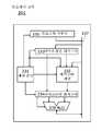
도 16의 (A)는 전자 부품의 제작 방법의 예를 나타낸 흐름도이다. 전자 부품은 반도체 패키지 또는 IC 패키지이라고도 한다. 이 전자 부품은 단자의 추출 방향 및 단자의 형상에 따라 복수의 규격 및 이름을 갖는다. 전자 부품의 예에 대하여 본 실시형태에서 설명한다.Fig. 16A is a flowchart showing an example of a method for manufacturing an electronic component. Electronic components are also referred to as semiconductor packages or IC packages. This electronic component has a plurality of specifications and names according to the extraction direction of the terminal and the shape of the terminal. An example of an electronic component is demonstrated in this embodiment.
트랜지스터를 포함하는 반도체 장치는, 조립 공정(후공정)을 거쳐, 탈착 가능한 부품을 프린트 배선 기판과 통합시킴으로써 완성된다. 후공정은 도 16의 (A)의 공정을 거쳐 마칠 수 있다. 구체적으로는, 웨이퍼 처리에서 얻어지는 소자 기판을 완성(공정 S1)시킨 후, 기판의 이면을 연삭한다(공정 S2). 이 공정에서 기판을 얇게 하여, 웨이퍼 공정에서의 기판의 굽힘 등을 저감하고, 전자 부품의 크기를 축소한다.A semiconductor device including a transistor is completed by integrating detachable parts with a printed wiring board through an assembly process (post-process). The post-process may be completed through the process of FIG. 16A. Specifically, after the element substrate obtained in the wafer processing is completed (Step S1), the back surface of the substrate is ground (Step S2). In this process, the substrate is made thin to reduce bending of the substrate in the wafer process, and the size of the electronic component is reduced.
기판의 이면을 연삭하여, 이 기판을 다이싱 공정에서 복수의 칩으로 분리한다. 다이 본딩 공정에서, 이 분리한 칩을 따로따로 픽업하여 리드 프레임에 탑재하고 접합한다(공정 S3). 다이 본딩 공정에서는, 제품에 따라 적절한 방법, 예를 들어 수지 또는 테이프에 의한 접합에 의하여 칩과 리드 프레임을 접합한다. 다이 본딩 공정에서, 칩을 인터포저 위에 탑재하여 접합하여도 좋다. 와이어 본딩 공정에서, 리드 프레임의 리드와 칩 위의 전극을 금속 세선(細線)(와이어)으로 전기적으로 접속시킨다(공정 S4). 금속 세선으로서는 은선 또는 금선을 사용할 수 있다. 와이어 본딩으로서는, 볼 본딩(ball bonding) 또는 웨지 본딩(wedge bonding)을 사용할 수 있다.The back surface of the substrate is ground, and the substrate is separated into a plurality of chips in the dicing process. In the die bonding step, the separated chips are picked up separately, mounted on a lead frame, and joined (step S3). In the die bonding step, the chip and the lead frame are joined by an appropriate method depending on the product, for example, bonding with resin or tape. In the die bonding process, the chip may be mounted on an interposer and joined. In the wire bonding step, the lead of the lead frame and the electrode on the chip are electrically connected with a thin metal wire (wire) (step S4). As the fine metal wire, a silver wire or a gold wire can be used. As wire bonding, ball bonding or wedge bonding can be used.
몰딩 공정은 와이어 본딩된 칩을 에폭시 수지 등으로 밀봉하기 위하여 수행된다(공정 S5). 몰딩 공정에 의하여 전자 부품은 수지로 채워져, 탑재된 회로부 또는 와이어에 대한 기계적 외력으로 인한 대미지를 저감시킬 수 있다. 또한, 수분 또는 먼지로 인한 특성 열화를 저감시킬 수 있다. 리드 프레임의 리드를 도금한다. 그 후, 리드를 절단하고 가공한다(공정 S6). 이 도금 처리에 의하여 리드의 녹을 방지하고, 나중의 공정에서 프린트 배선 기판에 칩을 탑재할 때의 납땜을 용이하게 한다. 프린팅(마킹)을 패키지 표면에 수행한다(공정 S7). 점검 공정(공정 S8)을 거쳐 전자 부품이 완성된다(공정 S9). 전자 부품이 본 실시형태에서 설명한 반도체 장치를 포함하면, 저전력이며 소형의 전자 부품을 제공할 수 있다.A molding process is performed to seal the wire-bonded chip with an epoxy resin or the like (step S5). The electronic component may be filled with resin by the molding process, thereby reducing damage due to mechanical external force to the mounted circuit unit or wire. In addition, deterioration of properties due to moisture or dust can be reduced. Plate the leads of the lead frame. Thereafter, the lead is cut and processed (Step S6). This plating process prevents rusting of the leads and facilitates soldering when mounting a chip on a printed wiring board in a later step. Printing (marking) is performed on the package surface (step S7). An electronic component is completed through an inspection process (process S8) (process S9). When the electronic component includes the semiconductor device described in the present embodiment, it is possible to provide a low-power and small-sized electronic component.
도 16의 (B)는 완성된 전자 부품의 개략 투시도이다. 도 16의 (B)는 전자 부품의 예로서 QFP(quad flat package)의 개략 투시도를 도시한 것이다. 도 16의 (B)에 도시된 바와 같이, 전자 부품(7000)은 리드(7001) 및 회로부(7003)를 포함한다. 회로부(7003)에서는 예를 들어, 실시형태 2에서 설명한 스캔 FF(SFF) 및 다른 논리 회로가 형성된다. 전자 부품(7000)은 예를 들어, 프린트 배선 기판(7002)에 탑재된다. 복수의 전자 부품(7000)이 조합되어 사용되고 프린트 배선 기판(7002) 위에서 서로 전기적으로 접속되면, 전자 부품(7000)을 전자 기기에 탑재할 수 있다. 완성된 회로 기판(7004)은 전자 기기 등 내에 제공된다. 전자 부품(7000)은 예를 들어, 데이터를 저장하는 랜덤 액세스 메모리, 또는 CPU, MCU(microcontroller unit), FPGA, 또는 무선 IC 등의 각종 처리를 실행하는 처리 유닛으로서 사용될 수 있다. 전자 기기가 전자 부품(7000)을 포함하면, 전자 기기의 소비전력을 저감시킬 수 있다. 또는 전자 기기를 소형으로 할 수 있다.Fig. 16B is a schematic perspective view of a completed electronic component. 16B is a schematic perspective view of a quad flat package (QFP) as an example of an electronic component. As shown in FIG. 16B , the
전자 부품(7000)은 디지털 신호 처리, 소프트웨어 정의 무선 시스템, 항공 전자 공학 시스템(통신 시스템, 항법 시스템, 자동 유도 시스템, 및 비행 관리 시스템 등, 항공기에 사용되는 전자 기기), ASIC 프로토타이핑, 의료 화상 처리, 음성 인식, 암호화, 바이오 정보 과학, 기계 시스템의 에뮬레이터, 및 전파 천문학에서의 전파 망원경 등, 폭넓은 분야에서의 전자 기기의 전자 부품(IC칩)으로서 사용될 수 있다. 이러한 전자 기기의 예에는 표시 장치, 퍼스널 컴퓨터(PC), 및 기록 매체가 제공된 화상 재생 장치(DVD, Blu-ray, 플래시 메모리, 및 HDD 등의 기록 매체의 내용을 재생하는 장치, 및 표시 화상을 표시하는 디스플레이)가 포함된다. 본 발명의 일 형태의 전자 부품이 제공될 수 있는 전자 기기의 다른 예에는, 휴대 전화, 휴대 게임기를 포함하는 게임기, 휴대 정보 기기, 전자책 리더, 카메라(예를 들어, 비디오 카메라 및 디지털 스틸 카메라), 웨어러블 표시 장치(예를 들어, 헤드마운트 표시 장치, 고글형 표시 장치, 안경형 표시 장치, 완장형 표시 장치, 팔찌형 표시 장치, 및 목걸이형 표시 장치), 항법 시스템, 음향 재생 장치(예를 들어, 카 오디오 시스템 및 디지털 오디오 플레이어), 복사기, 팩시밀리, 프린터, 프린터 복합기, 현금 자동 입출금기(ATM), 및 자동 판매기가 포함된다. 도 17의 (A) 내지 (H)는 이러한 전자 기기의 구체적인 예를 도시한 것이다.
도 17의 (A)의 휴대 게임기(900)는 하우징(901), 하우징(902), 표시부(903), 표시부(904), 마이크로폰(905), 스피커(906), 조작 키(907), 및 스타일러스(908) 등을 포함한다.The
도 17의 (B)의 휴대 정보 단말(910)은 하우징(911), 하우징(912), 표시부(913), 표시부(914), 연결 부위(915), 및 조작 키(916) 등을 포함한다. 표시부(913)는 하우징(911)에 제공되고 표시부(914)는 하우징(912)에 제공된다. 하우징(911) 및 하우징(912)은 연결 부위(915)에 의하여 서로 접속되고, 하우징(911)과 하우징(912) 사이의 각도는 연결 부위(915)에 의하여 변경될 수 있다. 표시부(913)에 표시되는 화상은 연결 부위(915)에서 하우징(911)과 하우징(912) 사이의 각도에 따라 전환될 수 있다. 터치 패널을 갖는 표시 장치는 표시부(913) 및/또는 표시부(914)로서 사용될 수 있다.The
도 17의 (C)의 노트북(920)은 하우징(921), 표시부(922), 키보드(923), 및 포인팅 디바이스(924) 등을 포함한다.The
도 17의 (D)의 전기 냉동 냉장고(930)는 하우징(931), 냉장고 도어(932), 및 냉동고 도어(933) 등을 포함한다.The
도 17의 (E)의 비디오 카메라(940)는 하우징(941), 하우징(942), 표시부(943), 조작 키(944), 렌즈(945), 및 연결 부위(946) 등을 포함한다. 조작 키(944) 및 렌즈(945)는 하우징(941)에 제공되고, 표시부(943)는 하우징(942)에 제공된다. 하우징(941) 및 하우징(942)은 연결 부위(946)에 의하여 서로 연결되고, 하우징(941)과 하우징(942) 사이의 각도는 연결 부위(946)에 의하여 변경될 수 있다. 하우징(941)과 하우징(942) 사이의 각도에 따라, 예를 들어 표시부(943)에 표시되는 화상의 방향이 변경될 수 있고 화상의 표시 및 비표시가 전환될 수 있다.The
도 17의 (F)의 자동차(950)는 차체(951), 차륜(952), 대시보드(953), 및 라이트(954) 등을 포함한다.The
(실시형태 4)(Embodiment 4)
본 실시형태에서는, 산화물 반도체 및 OS 트랜지스터 등에 대하여 설명한다.In this embodiment, an oxide semiconductor, an OS transistor, and the like will be described.
<OS 트랜지스터의 구조예 1><Structure Example 1 of OS Transistor>
도 18의 (A) 내지 (D)는 OS 트랜지스터의 구조예를 도시한 것이다. 도 18의 (A)는 OS 트랜지스터의 구조예를 도시한 상면도이다. 도 18의 (B)는 도 18의 (A)의 선 y1-y2를 따라 취한 단면도이다. 도 18의 (C)는 도 18의 (A)의 선 x1-x2를 따라 취한 단면도이다. 도 18의 (D)는 도 18의 (A)의 선 x3-x4를 따라 취한 단면도이다. 선 y1-y2의 방향을 채널 길이 방향이라고 하고, 선 x1-x2의 방향을 채널 폭 방향이라고 하는 경우가 있다. 따라서, 도 18의 (B)에는 채널 길이 방향에서의 OS 트랜지스터의 단면도를 도시하고, 도 18의 (C) 및 (D)에는 각각 채널 폭 방향에서의 OS 트랜지스터의 단면 구조를 도시하였다. 또한, 디바이스 구조를 명확하게 하기 위하여, 도 18의 (A)에는 일부 구성요소를 도시하지 않았다.18A to 18D show a structural example of an OS transistor. 18A is a top view showing a structural example of an OS transistor. FIG. 18B is a cross-sectional view taken along line y1-y2 of FIG. 18A. Fig. 18(C) is a cross-sectional view taken along the line x1-x2 of Fig. 18(A). Fig. 18(D) is a cross-sectional view taken along the line x3-x4 of Fig. 18(A). The direction of the line y1-y2 is referred to as a channel length direction, and the direction of the line x1-x2 is referred to as a channel width direction in some cases. Accordingly, FIG. 18B shows a cross-sectional view of the OS transistor in the channel length direction, and FIGS. 18C and 18D show a cross-sectional structure of the OS transistor in the channel width direction, respectively. In addition, in order to clarify the device structure, some components are not shown in FIG. 18A.
OS 트랜지스터(501)는 절연 표면 위, 여기서는 절연층(511) 위에 형성된다. 절연층(511)은 기판(510)의 표면 위에 형성된다. OS 트랜지스터(501)는 절연층(514) 및 절연층(515)으로 덮인다. 또한, 절연층(514 및 515)은 OS 트랜지스터(501)의 구성요소로서 간주할 수 있다. OS 트랜지스터(501)는 절연층(512), 절연층(513), 산화물 반도체(OS)층(521 내지 523), 도전층(530), 도전층(541), 및 도전층(542)을 포함한다. 절연층(513)은 게이트 절연층으로서 기능하는 영역을 포함한다. 도전층(530)은 게이트 전극으로서 기능한다. 도전층(531)은 백 게이트 전극으로서 기능한다. 여기서, OS층(521 내지 523)을 통합적으로 OS층(520)이라고 부른다.An
도 18의 (B) 및 (C)에 도시된 바와 같이, OS층(520)은 OS층(521), OS층(522), 및 OS층(523)이 이 순서대로 적층된 영역을 포함한다. 절연층(513)은 이 적층 영역을 덮는다. 도전층(531)은 절연층(513)을 개재(介在)하여 적층 영역과 중첩된다. 도전층(541) 및 도전층(542)은 OS층(521) 및 OS층(523)으로 형성된 적층 위에 제공되고, 이 적층의 상면 및 적층의 채널 길이 방향에 위치하는 측면과 접한다. 도 18의 (A) 내지 (D)의 예에서는, 도전층(541 및 542)은 절연층(512)과도 접한다. OS층(523)은 OS층(521 및 522) 및 도전층(541 및 542)을 덮도록 형성된다. OS층(523)의 하면은 OS층(522)의 상면과 접한다.As shown in (B) and (C) of FIG. 18 , the
도전층(530)은 절연층(513)을 개재하여, OS층(520)에서 OS층들(521 내지 523)이 적층된 영역을 채널 폭 방향으로 둘러싸도록 형성된다(도 18의 (C) 참조). 따라서, 수직 방향의 게이트 전계 및 횡 방향의 게이트 전계가 이 적층 영역에 인가된다. OS 트랜지스터(501)에서, 게이트 전계란 도전층(530)(게이트 전극층)에 인가되는 전압에 의하여 생성되는 전계를 말한다. 따라서, OS층(521 내지 523)의 적층 영역 전체를 게이트 전계에 의하여 전기적으로 둘러쌀 수 있기 때문에, OS층(522) 전체(벌크)에 채널이 형성되는 경우가 있다. 따라서 OS 트랜지스터(501)는 높은 온 전류를 가질 수 있다.The
본 명세서에서, 상술한 트랜지스터와 같이 게이트 전계에 의하여 반도체가 전기적으로 둘러싸이는 트랜지스터의 구조를 s-channel(surrounded channel) 구조라고 한다. OS 트랜지스터(501)는 s-channel 구조를 갖는다. 이 s-channel 구조에 의하여, 많은 양의 전류가 트랜지스터의 소스와 드레인 사이를 흐를 수 있어, 온 상태에서의 드레인 전류(온 전류)를 높일 수 있다.In the present specification, a structure of a transistor in which a semiconductor is electrically surrounded by a gate electric field like the above-described transistor is referred to as an s-channel (surrounded channel) structure. The
OS 트랜지스터(501)의 s-channel 구조는 OS층(522)의 측면에도 게이트 전계가 인가되게 하여, 채널 형성 영역의 제어가 쉬워진다. 도전층(530)이 OS층(522) 아래에 도달하고 OS층(521)의 측면과 대향하는 구조에서는, 높은 제어성을 달성할 수 있어 바람직하다. 결과적으로 OS 트랜지스터(501)의 S값(subthreshold swing)을 작게 할 수 있어, 단채널 효과를 저감시킬 수 있다. 따라서, s-channel 구조는 소형화에 적합하다.The s-channel structure of the
OS 트랜지스터(501)와 같이, OS 트랜지스터가 입체적인 구조를 갖는 경우, 채널 길이는 100nm 미만으로 할 수 있다. OS 트랜지스터를 소형화함으로써, 회로 면적을 작게 할 수 있다. OS 트랜지스터의 채널 길이는 65nm 미만이 바람직하고, 30nm 이하 또는 20nm 이하가 더 바람직하다. 채널 길이는 적어도 10nm이다.When the OS transistor has a three-dimensional structure like the
트랜지스터의 게이트로서 기능하는 도전체, 트랜지스터의 소스로서 기능하는 도전체, 및 트랜지스터의 드레인으로서 기능하는 도전체를 각각 게이트 전극, 소스 전극, 및 드레인 전극이라고 한다. 트랜지스터의 소스로서 기능하는 영역 및 트랜지스터의 드레인으로서 기능하는 영역은 각각 소스 영역 및 드레인 영역이라고 한다. 본 명세서에서는, 게이트 전극을 게이트라고 할 수 있고, 드레인 전극 또는 드레인 영역을 드레인이라고 할 수 있고, 소스 전극 또는 소스 영역을 소스라고 할 수 있다.The conductor functioning as the gate of the transistor, the conductor functioning as the source of the transistor, and the conductor functioning as the drain of the transistor are referred to as a gate electrode, a source electrode, and a drain electrode, respectively. The region serving as the source of the transistor and the region serving as the drain of the transistor are referred to as a source region and a drain region, respectively. In this specification, the gate electrode may be referred to as a gate, the drain electrode or the drain region may be referred to as a drain, and the source electrode or the source region may be referred to as a source.
채널 길이란, 예를 들어, 트랜지스터의 상면에서 반도체(또는 트랜지스터가 온일 때 전류가 반도체를 흐르는 부분)와 게이트 전극이 서로 중첩되는 영역 또는 채널이 형성되는 영역의 소스와 드레인 사이의 거리를 말한다. 하나의 트랜지스터에서, 모든 영역의 채널 길이가 반드시 같을 필요는 없다. 바꿔 말하면, 하나의 트랜지스터의 채널 길이는 하나의 값에 고정되지 않는 경우가 있다. 따라서, 본 명세서에서 채널 길이는 채널이 형성되는 영역에서의 어느 하나의 값, 최대값, 최소값, 또는 평균값이다.The channel length refers to, for example, a distance between a source and a drain in a region where a semiconductor (or a portion through which a current flows when the transistor is on) and a gate electrode overlap each other on the upper surface of a transistor or a region in which a channel is formed. In one transistor, the channel lengths of all regions are not necessarily the same. In other words, there are cases where the channel length of one transistor is not fixed to one value. Accordingly, in the present specification, the channel length is any one value, a maximum value, a minimum value, or an average value in a region where a channel is formed.
채널 폭이란, 예를 들어, 반도체(또는 트랜지스터가 온일 때 전류가 반도체를 흐르는 부분)와 게이트 전극이 서로 중첩되는 영역 또는 채널이 형성되는 영역에서 소스와 드레인이 서로 대향하는 부분의 길이를 말한다. 하나의 트랜지스터에서, 모든 영역의 채널 폭이 반드시 같은 값을 가질 필요는 없다. 바꿔 말하면, 하나의 트랜지스터의 채널 폭은 하나의 값에 고정되지 않는 경우가 있다. 따라서, 본 명세서에서 채널 폭은 채널이 형성되는 영역에서의 어느 하나의 값, 최대값, 최소값, 또는 평균값이다.The channel width refers to, for example, a length of a portion where a source and a drain face each other in a region where a semiconductor (or a portion through which a current flows when a transistor is on) and a gate electrode overlap each other or a region where a channel is formed. In one transistor, the channel widths of all regions do not necessarily have the same value. In other words, there are cases where the channel width of one transistor is not fixed to one value. Accordingly, in the present specification, the channel width is any one value, a maximum value, a minimum value, or an average value in a region where a channel is formed.
또한, 트랜지스터의 구조에 따라서는, 채널이 실제로 형성되는 영역에서의 채널 폭(이하, 실효적인 채널 폭이라고 함)은, 트랜지스터의 상면도에 나타내어지는 채널 폭(이하, 외견상 채널 폭이라고 함)과 상이한 경우가 있다. 예를 들어, 입체적인 구조를 갖는 트랜지스터에서는, 실효적인 채널 폭이 트랜지스터의 상면도에 나타내어지는 외견상 채널 폭보다 크고, 그 영향을 무시할 수 없는 경우가 있다. 예를 들어, 입체적인 구조를 갖는 소형화된 트랜지스터에서는, 반도체의 측면에 형성되는 채널 영역의 비율이 증가되는 경우가 있다. 이 경우, 채널이 실제로 형성될 때 얻어지는 실효적인 채널 폭은 상면도에 나타내어지는 외견상 채널 폭보다 크다.In addition, depending on the structure of the transistor, the channel width in the region where the channel is actually formed (hereinafter referred to as effective channel width) is the channel width shown in the top view of the transistor (hereinafter referred to as apparent channel width) may be different from For example, in a transistor having a three-dimensional structure, the effective channel width is larger than the apparent channel width shown in the top view of the transistor, and the influence thereof cannot be ignored in some cases. For example, in a miniaturized transistor having a three-dimensional structure, the ratio of a channel region formed on a side surface of a semiconductor may increase. In this case, the effective channel width obtained when the channel is actually formed is larger than the apparent channel width shown in the top view.
입체적인 구조를 갖는 트랜지스터에서는, 실효적인 채널 폭을 측정하기가 어려운 경우가 있다. 예를 들어, 설계값으로부터의 실효적인 채널 폭을 추산하기 위해서는, 반도체의 형상이 알려져 있다고 상정할 필요가 있다. 따라서, 반도체의 형상이 정확히 알려져 있지 않은 경우에는, 실효적인 채널 폭을 정확히 측정하기 어렵다.In a transistor having a three-dimensional structure, it may be difficult to measure the effective channel width. For example, in order to estimate the effective channel width from the design value, it is necessary to assume that the shape of the semiconductor is known. Therefore, when the shape of the semiconductor is not precisely known, it is difficult to accurately measure the effective channel width.
따라서 본 명세서에서는, 트랜지스터의 상면도에 있어서, 반도체와 게이트 전극이 서로 중첩되는 영역에서 소스와 드레인이 서로 대향하는 부분의 길이인 외견상 채널 폭을 SCW(surrounded channel width)라고 하는 경우가 있다. 또한, 본 명세서에서 '채널 폭'이라는 용어는 SCW, 즉 외견상 채널 폭 또는 실효적인 채널 폭을 나타낼 수 있다. 또한, 채널 길이, 채널 폭, 실효적인 채널 폭, 외견상 채널 폭, SCW 등의 값은 단면 TEM 이미지 등을 얻고 분석함으로써 결정할 수 있다.Therefore, in the present specification, in the top view of the transistor, the apparent channel width, which is the length of the portion where the source and the drain face each other in the region where the semiconductor and the gate electrode overlap each other, is sometimes referred to as a surround channel width (SCW). Also, in this specification, the term 'channel width' may refer to SCW, that is, an apparent channel width or an effective channel width. In addition, values of channel length, channel width, effective channel width, apparent channel width, SCW, etc. can be determined by obtaining and analyzing a cross-sectional TEM image or the like.
트랜지스터의 전계 효과 이동도, 및 채널 폭당 전류값 등을 계산하기 위하여 SCW를 사용할 수 있다. 이러한 경우에는, 얻어지는 값은 시뮬레이션에 실효적인 채널 폭을 사용하여 얻어지는 값과 상이한 경우가 있다.SCW may be used to calculate the field-effect mobility of the transistor, the current value per channel width, and the like. In this case, the value obtained may be different from the value obtained using the effective channel width for the simulation.
<기판><substrate>
기판(510)은 단순한 지지 기판에 한정되지 않고, 트랜지스터 등의 장치가 형성되는 기판이어도 좋다. 이 경우, OS 트랜지스터(501)의 도전층(530), 도전층(541), 및 도전층(542) 중 하나는 상기 장치와 전기적으로 접속되어도 좋다.The
<하지 절연층><Sub Insulation Layer>
절연층(511)은 기판(510)으로부터의 불순물 확산을 방지하는 기능을 갖는다. 절연층(512)은 OS층(520)에 산소를 공급하는 기능을 갖는 것이 바람직하다. 이 때문에, 절연층(512)은 산소를 포함하는 절연막인 것이 바람직하고, 산소 함유량이 화학량론적 조성보다 높은 산소를 포함하는 절연막인 것이 더 바람직하다. 예를 들어, TDS(thermal desorption spectroscopy)에서, 막의 표면 온도가 100℃ 이상 700℃ 이하 또는 100℃ 이상 500℃ 이하일 때 1.0×10¹⁸분자/cm3 이상의 산소 분자가 방출되는 막을 사용할 수 있다. 기판(510)이 상술한 바와 같이 디바이스가 형성된 기판인 경우, 절연층(511)은 평평한 표면을 갖도록 CMP(chemical mechanical polishing) 등의 평탄화 처리가 수행되는 것이 바람직하다.The insulating
절연층(511 및 512)은 산화 알루미늄, 산화질화 알루미늄, 산화 마그네슘, 산화 실리콘, 산화질화 실리콘, 질화산화 실리콘, 산화 갈륨, 산화 저마늄, 산화 이트륨, 산화 지르코늄, 산화 란타넘, 산화 네오디뮴, 산화 하프늄, 산화 탄탈럼, 질화 실리콘, 또는 질화산화 알루미늄 등의 절연 재료, 또는 이들 재료의 혼합 재료를 사용하여 형성될 수 있다.The insulating
<게이트 전극><Gate electrode>
도전층(530)은 구리(Cu), 텅스텐(W), 몰리브데넘(Mo), 금(Au), 알루미늄(Al), 망가니즈(Mn), 타이타늄(Ti), 탄탈럼(Ta), 니켈(Ni), 크로뮴(Cr), 납(Pb), 주석(Sn), 철(Fe), 코발트(Co), 루테늄(Ru), 이리듐(Ir), 스트론튬(Sr), 또는 백금(Pt) 등의 금속, 이들 금속 중 어느 것의 합금, 또는 이들 금속 중 어느 것을 주성분으로서 포함하는 화합물을 사용하여 형성되는 것이 바람직하다.The
도전층(530)은 단층 구조 또는 2층 이상의 층상 구조를 가져도 좋다. 예를 들어, 이하의 구조 중 어느 것을 채용할 수 있다: 실리콘을 포함하는 알루미늄막의 단층 구조; 타이타늄막이 알루미늄막 위에 적층된 2층 구조; 타이타늄막이 질화 타이타늄막 위에 적층된 2층 구조; 텅스텐막이 질화 타이타늄막 위에 적층된 2층 구조; 텅스텐막이 질화 탄탈럼막 또는 질화 텅스텐막 위에 적층된 2층 구조; 타이타늄막, 알루미늄막, 및 타이타늄막이 이 순서대로 적층된 3층 구조; Cu-Mn 합금막의 단층 구조; Cu막이 Cu-Mn 합금막 위에 적층된 2층 구조; 및 Cu-Mn 합금막, Cu막, 및 Cu-Mn 합금막이 이 순서대로 적층된 3층 구조. Cu-Mn 합금막은 전기 저항이 낮고, 산소를 포함하는 절연막과의 계면에 산화 망가니즈를 형성하고, 산화 망가니즈는 Cu 확산을 방지할 수 있기 때문에 바람직하게 사용된다.The
도전층(530)은 인듐 주석 산화물, 산화 텅스텐을 포함하는 인듐 산화물, 산화 텅스텐을 포함하는 인듐 아연 산화물, 산화 타이타늄을 포함하는 인듐 산화물, 산화 타이타늄을 포함하는 인듐 주석 산화물, 인듐 아연 산화물, 또는 산화 실리콘이 첨가된 인듐 주석 산화물 등의 투광성 도전 재료를 사용하여 형성될 수도 있다. 상기 투광성 도전 재료 및 상기 금속 원소를 사용하여 형성된 층상 구조를 가질 수도 있다.The
<게이트 절연층><Gate Insulation Layer>
절연층(513)은 단층 구조 또는 층상 구조를 갖는 절연막을 사용하여 형성된다. 절연층(513)은 산화 알루미늄, 산화 마그네슘, 산화 실리콘, 산화질화 실리콘, 질화산화 실리콘, 질화 실리콘, 산화 갈륨, 산화 저마늄, 산화 이트륨, 산화 지르코늄, 산화 란타넘, 산화 네오디뮴, 산화 하프늄, 및 산화 탄탈럼 중 적어도 하나를 포함하는 절연막을 사용하여 형성될 수 있다. 절연층(513)은 상술한 재료 중 어느 것을 포함하는 적층이어도 좋다. 절연층(513)은 란타넘(La), 질소, 또는 지르코늄(Zr) 등을 불순물로서 포함하여도 좋다. 절연층(511)은 절연층(513)과 마찬가지로 형성될 수 있다. 절연층(511)은 예를 들어, 산소, 질소, 실리콘, 또는 하프늄 등을 포함한다. 구체적으로는, 절연층(511)은 산화 하프늄, 및 산화 실리콘 또는 산화질화 실리콘을 포함하는 것이 바람직하다.The insulating
산화 하프늄은 산화 실리콘 및 산화질화 실리콘보다 유전율이 높다. 따라서, 산화 하프늄을 사용한 절연층(513)은 산화 실리콘을 사용한 절연층(513)보다 두께를 크게 할 수 있기 때문에, 터널 전류로 인한 누설 전류를 저감시킬 수 있다. 즉, 오프 전류가 낮은 트랜지스터를 제공할 수 있다. 또한, 결정 구조를 갖는 산화 하프늄은 비정질 구조를 갖는 산화 하프늄보다 유전율이 높다. 따라서, 오프 전류가 낮은 트랜지스터를 제공하기 위하여 결정 구조를 갖는 산화 하프늄을 사용하는 것이 바람직하다. 결정 구조의 예에는 단사정 구조 및 입방정 구조가 포함된다. 또한, 본 발명의 일 형태는 상술한 예에 한정되지 않는다.Hafnium oxide has a higher dielectric constant than silicon oxide and silicon oxynitride. Accordingly, since the insulating
<소스 전극, 드레인 전극, 백 게이트 전극><Source electrode, drain electrode, back gate electrode>
도전층(541 및 542)은 도전층(530)과 마찬가지로 형성할 수 있다. Cu-Mn 합금막은 전기 저항이 낮고, 산화물 반도체막과 접하여 형성될 때 산화물 반도체막과의 계면에 산화 망가니즈를 형성할 수 있고, 그리고 산화 망가니즈가 Cu의 확산을 방지할 수 있기 때문에 도전층(541 및 542)에 바람직하게 사용된다. 또한, 후술하는 도전층(531)(도 20의 (A) 참조)은 도전층(530)과 마찬가지로 형성할 수 있다.The
<보호 절연막><Protective Insulation Film>
절연층(514)은 산소, 수소, 물, 알칼리 금속, 및 알칼리 토금속 등을 차단하는 기능을 갖는 것이 바람직하다. 절연층(514)은 OS층(520)으로부터의 산소의 외부 확산 및 외부로부터 OS층(520)으로의 수소 또는 물 등의 진입을 방지할 수 있다. 절연층(514)은 예를 들어, 질화물 절연막일 수 있다. 상기 질화물 절연막은 질화 실리콘, 질화산화 실리콘, 질화 알루미늄, 또는 질화산화 알루미늄 등을 사용하여 형성된다. 또한, 산소, 수소, 물, 알칼리 금속, 및 알칼리 토금속 등에 대한 차단 효과를 갖는 질화물 절연막 대신에, 산소, 수소, 및 물 등에 대한 차단 효과를 갖는 산화물 절연막을 제공하여도 좋다. 산소, 수소, 및 물 등에 대한 차단 효과를 갖는 산화물 절연막으로서는, 산화 알루미늄막, 산화질화 알루미늄막, 산화 갈륨막, 산화질화 갈륨막, 산화 이트륨막, 산화질화 이트륨막, 산화 하프늄막, 및 산화질화 하프늄막을 사용할 수 있다.The insulating
산화 알루미늄막은 수소 및 수분 등 불순물 및 산소의 양쪽의 투과를 방지하는 데에 매우 효과적이기 때문에, 절연층(514)으로서 바람직하게 사용된다. 이로써, 산화 알루미늄막은, 트랜지스터의 제작 공정 중 및 그 후에, 트랜지스터의 전기 특성의 변화를 일으키는 수소 및 수분 등 불순물의 OS층(520)으로의 진입 방지, OS층(520)의 주성분인 산소의 산화물 반도체로부터의 방출 방지, 및 절연층(512)으로부터의 산소의 필요 없는 방출 방지의 효과를 갖는 보호막으로서 적합하게 기능할 수 있다. 또한, 산화 알루미늄막에 포함되는 산소를 산화물 반도체로 확산시킬 수 있다.The aluminum oxide film is preferably used as the insulating
<층간 절연막><Interlayer Insulation Film>
절연층(514) 위에 절연층(515)이 형성되는 것이 바람직하다. 절연층(515)은 단층 구조 또는 적층 구조의 절연막을 사용하여 형성할 수 있다. 이 절연층은 산화 마그네슘, 산화 실리콘, 산화질화 실리콘, 질화산화 실리콘, 질화 실리콘, 산화 갈륨, 산화 저마늄, 산화 이트륨, 산화 지르코늄, 산화 란타넘, 산화 네오디뮴, 산화 하프늄, 및 산화 탄탈럼 중 하나 이상을 포함하는 절연막을 사용하여 형성할 수 있다.The insulating
<산화물 반도체층><Oxide semiconductor layer>
OS층(521 내지 523)의 반도체 재료로서, 대표적으로는, In-Ga 산화물, In-Zn 산화물, 또는 In-M-Zn 산화물(M은 Ga, Y, Sn, Zr, La, Ce, 또는 Nd 등)을 사용한다. 원소 M은, 예를 들어, 산소와의 결합 에너지가 높은 원소이다. 원소 M은 산소와의 결합 에너지가 인듐보다 높은 원소이다. 또는, 원소 M은 산화물 반도체의 에너지 갭을 증대시킬 수 있는 원소이다. 또한, OS층(521 내지 523)은 인듐을 포함하는 산화물층에 한정되지 않는다. OS층(521 내지 523)은 예를 들어, Zn-Sn 산화물층, Ga-Sn 산화물층, 또는 Zn-Mg 산화물을 사용하여 형성할 수 있다. OS층(522)은 In-M-Zn 산화물을 사용하여 형성되는 것이 바람직하다. OS층(521 및 523)은 Ga 산화물을 사용하여 형성할 수 있다.As a semiconductor material of the OS layers 521 to 523, representatively, In-Ga oxide, In-Zn oxide, or In-M-Zn oxide (M is Ga, Y, Sn, Zr, La, Ce, or Nd) etc) is used. The element M is, for example, an element with high binding energy with oxygen. Element M is an element having a higher bonding energy with oxygen than indium. Alternatively, the element M is an element capable of increasing the energy gap of the oxide semiconductor. In addition, the OS layers 521 to 523 are not limited to oxide layers containing indium. The OS layers 521 to 523 may be formed using, for example, a Zn-Sn oxide layer, a Ga-Sn oxide layer, or a Zn-Mg oxide. The
OS층(522)은 인듐을 포함하는 산화물 반도체에 한정되지 않는다. OS층(522)은 예를 들어 인듐을 포함하지 않고 아연, 갈륨, 및 주석 중 적어도 하나를 포함하는 산화물 반도체(예를 들어 아연 주석 산화물 또는 갈륨 주석 산화물)이어도 좋다.The
OS층(522)에는 에너지 갭이 넓은 산화물을 사용할 수 있다. OS층(522)의 에너지 갭은 예를 들어 2.5eV 이상 4.2eV 이하, 바람직하게는 2.8eV 이상 3.8eV 이하, 더 바람직하게는 3eV 이상 3.5eV 이하이다.An oxide having a wide energy gap may be used for the
OS층(522)은 후술하는 CAAC-OS막인 것이 바람직하다. 산화물 반도체가 Zn을 포함하면, 산화물 반도체는 결정화되기 쉬운 경우가 있다. 따라서, OS층(522)은 Zn을 포함하는 것이 바람직하다.The
OS층(522)과 OS층(521) 사이의 계면에 계면 준위가 형성되면, 이 계면에 가까운 영역에 채널 영역도 형성되기 때문에, OS 트랜지스터(501)의 문턱 전압이 변화된다. OS층(521)은 OS층(522)에 포함되는 금속 원소 중 적어도 하나를 포함하는 것이 바람직하다. 따라서, OS층(522)과 OS층(523) 사이의 계면에 계면 준위가 거의 형성되지 않아, 문턱 전압 등 OS 트랜지스터(501)의 전기 특성의 편차를 저감시킬 수 있다.When an interface level is formed at the interface between the
OS층(522)과 OS층(523) 사이의 계면에서 계면 산란이 일어나기 어렵고, 캐리어 이동이 저해되지 않기 때문에, OS층(523)은 OS층(522)에 포함되는 금속 원소 중 적어도 하나를 포함하는 것이 바람직하다. 그러므로, OS 트랜지스터(501)의 전계 효과 이동도를 높일 수 있다.Since interfacial scattering hardly occurs at the interface between the
OS층(521, 522, 및 523)은 적어도 인듐을 포함하는 것이 바람직하다. OS층(521)으로서 In-M-Zn 산화물을 사용하는 경우, In과 M의 총 비율을 100atomic%로 상정할 때, In의 비율을 50atomic% 미만, M의 비율을 50atomic%보다 높게 하는 것이 바람직하고, In의 비율을 25atomic% 미만, M의 비율을 75atomic%보다 높게 하는 것이 더 바람직하다. OS층(522)으로서 In-M-Zn 산화물을 사용하는 경우, In과 M의 총 비율을 100atomic%로 상정할 때, In의 비율을 25atomic%보다 높게, M의 비율을 75atomic% 미만으로 하는 것이 바람직하고, In의 비율을 34atomic%보다 높게,M의 비율을 66atomic% 미만으로 하는 것이 더 바람직하다. OS층(523)으로서 In-M-Zn 산화물을 사용하는 경우, In과 M의 총 비율을 100atomic%로 상정할 때, In의 비율을 50atomic% 미만, M의 비율을 50atomic%보다 높게 하는 것이 바람직하고, In의 비율을 25atomic% 미만, M의 비율을 75atomic%보다 높게 하는 것이 더 바람직하다. 또한, OS층(523)은 OS층(521)과 같은 종류의 산화물이어도 좋다. 또는, OS층(521) 및/또는 OS층(523)은 인듐을 포함하지 않아도 되는 경우가 있다. 예를 들어, OS층(521) 및/또는 OS층(523)은 산화 갈륨을 사용하여 형성할 수 있다.The OS layers 521, 522, and 523 preferably contain at least indium. In the case of using In-M-Zn oxide as the
OS층(521 내지 523) 중에서 OS층(522)이 가장 높은 캐리어 이동도를 갖는 것이 바람직하다. 이로써, 절연층(511)으로부터 떨어져 있는 OS층(522)에 채널을 형성할 수 있다.Among the OS layers 521 to 523, the
예를 들어, In-M-Zn 산화물 등 In을 포함하는 산화물에서는, In 함유량의 증가에 의하여 캐리어 이동도가 높아질 수 있다. In-M-Zn 산화물에서는, 주로 중금속의 s 궤도가 캐리어 이동에 기여하고, 산화물 반도체 내의 인듐 함유량이 증가되면, In 원자의 s 궤도의 중첩이 증가된다. 따라서, 인듐의 함유량이 높은 산화물은 인듐의 함유량이 낮은 산화물보다 이동도가 높다. 그러므로, 인듐의 함유량이 높은 산화물을 산화물 반도체막으로서 사용하여, 캐리어 이동도를 높일 수 있다.For example, inan oxide containing In, such as an In-M- Zn oxide, carrier mobility may be increased by an increase in the In content. In In-M- Zn oxide, mainly the s orbitals of heavy metals contribute to carrier movement, and when the indium content in the oxide semiconductor is increased, the overlap of the s orbitals of In atoms is increased. Accordingly, an oxide having a high indium content has a higher mobility than an oxide having a low indium content. Therefore, carrier mobility can be improved by using an oxide with a high indium content as the oxide semiconductor film.
산화물 반도체막을 스퍼터링에 의하여 퇴적시킬 때, 기판 표면(산화물 반도체막이 퇴적되는 표면)의 가열 또는 공간 가열 등에 의하여, 막의 조성이 소스인 타깃 등의 조성과 상이한 경우가 있다. 예를 들어, In-Ga-Zn 산화물의 타깃을 사용하는 경우, 산화 아연은 산화 인듐 또는 산화 갈륨 등보다 승화되기 쉽기 때문에, 소스 및 In-Ga-Zn 산화물이 상이한 조성을 갖기 쉽다. 구체적으로는, In-Ga-Zn 산화물에서 Zn의 함유량이 소스보다 낮다. 따라서, 소스는 조성의 변화를 미리 고려하여 선택하는 것이 바람직하다. 또한, 소스와 막의 조성의 차이는 온도에 더하여 압력 또는 퇴적에 사용되는 가스에 의해서도 영향을 받는다.When the oxide semiconductor film is deposited by sputtering, the composition of the film may be different from the composition of the target or the like as the source due to heating or space heating of the substrate surface (the surface on which the oxide semiconductor film is deposited). For example, when a target of In-Ga-Zn oxide is used, since zinc oxide is more likely to sublimate than indium oxide or gallium oxide, the source and In-Ga-Zn oxide tend to have different compositions. Specifically, the content of Zn in the In-Ga-Zn oxide is lower than that of the source. Therefore, it is preferable to select the source in consideration of the change in composition in advance. In addition, the difference in the composition of the source and the film is affected by the pressure or the gas used for deposition in addition to the temperature.
OS층(522)이, 스퍼터링에 의하여 형성된 In-M-Zn 산화물인 경우, In-M-Zn 산화물을 퇴적시키기 위하여 사용되는 타깃의 금속 원소의 원자수비가 In:M:Zn=1:1:1, 3:1:2, 또는 4:2:4.1인 것이 바람직하다. 예를 들어, In:M:Zn=4:2:4.1의 타깃을 사용하여 퇴적된 반도체막에 포함되는 금속 원소의 원자수비는 약 In:M:Zn=4:2:3이다.When the
OS층(521 및 523) 각각이 스퍼터링에 의하여 형성된 In-M-Zn 산화물인 경우, In-M-Zn 산화물을 퇴적시키기 위하여 사용되는 타깃의 금속 원소의 원자수비가 In:M:Zn=1:3:2 또는 1:3:4인 것이 바람직하다.When each of the OS layers 521 and 523 is an In-M-Zn oxide formed by sputtering, the atomic ratio of the metal element of the target used for depositing the In-M-Zn oxide is In:M:Zn=1: 3:2 or 1:3:4 is preferred.
산화물 반도체막을 스퍼터링에 의하여 형성하는 경우, 플라스마를 발생시키기 위한 전원은 적절히 RF 전원, AC 전원, 또는 DC 전원 등으로 할 수 있다. 스퍼터링 가스로서, 희가스(대표적으로 아르곤), 산소 가스, 또는 희가스와 산소의 혼합 가스를 적절히 사용한다. 희가스와 산소의 혼합 가스를 사용하는 경우, 희가스에 대한 산소의 비율을 증가시키는 것이 바람직하다. 또한 타깃은 형성하는 산화물 반도체의 조성에 따라 적절히 선택하면 좋다.In the case where the oxide semiconductor film is formed by sputtering, the power source for generating the plasma may be appropriately an RF power supply, an AC power supply, or a DC power supply. As the sputtering gas, a noble gas (typically argon), oxygen gas, or a mixed gas of a rare gas and oxygen is appropriately used. When a mixed gas of rare gas and oxygen is used, it is preferable to increase the ratio of oxygen to the rare gas. In addition, what is necessary is just to select a target suitably according to the composition of the oxide semiconductor to form.
고순도 진성 또는 실질적으로 고순도 진성의 산화물 반도체막을 형성하기 위해서는, 체임버를 고진성으로 배기하는 것 외에 스퍼터링 가스를 고순도화할 필요가 있다. 스퍼터링 가스로서 사용되는 산소 가스 또는 아르곤 가스를 이슬점이 -40℃ 이하, 바람직하게는 80℃ 이하, 더 바람직하게는 -100℃ 이하가 되도록 고순도화함으로써, 산화물 반도체로의 수분 등의 침입을 가능한 한 방지할 수 있다.In order to form a high-purity intrinsic or substantially high-purity intrinsic oxide semiconductor film, it is necessary to purify the sputtering gas in addition to evacuating the chamber to high intrinsic nature. By purifying the oxygen gas or argon gas used as the sputtering gas so that the dew point is -40°C or less, preferably 80°C or less, and more preferably -100°C or less, the penetration of moisture into the oxide semiconductor is as much as possible. can be prevented
<에너지 밴드 구조><Energy band structure>
다음에, OS층(521), OS층(522), 및 OS층(523)이 적층되는 OS층(520)의 기능 및 효과에 대하여 도 19의 (B)의 에너지 밴드도를 사용하여 설명한다. 도 19의 (A)는 도 18의 (B)의 OS 트랜지스터(502)의 채널 영역의 부분 확대도이다. 도 19의 (B)는 도 19의 (A)에서 점선 z1-z2를 따른 부분(OS 트랜지스터(502)의 채널 형성 영역)의 에너지 밴드도를 나타낸 것이다. 아래에서 OS 트랜지스터(501)를 일례로서 설명하지만, 이것은 OS 트랜지스터(502 내지 506)에도 마찬가지로 적용된다.Next, the functions and effects of the
도 19의 (B)에 있어서, Ec512, Ec521, Ec522, Ec523, 및 Ec513은 각각 절연층(512), OS층(521), OS층(522), OS층(523), 및 절연층(513)의 전도대 하단의 에너지를 나타낸다.In FIG. 19B , Ec512, Ec521, Ec522, Ec523, and Ec513 are an insulating
여기서, 진공 준위와 전도대 하단 사이의 에너지 차이(이 차이를 전자 친화력이라고도 함)는 진공 준위와 가전자대 상단 사이의 에너지 차이(이 차이를 이온화 전위라고도 함)에서 에너지 갭을 뺌으로써 얻어진 값에 상당한다. 에너지 갭은 분광 타원해석기(HORIBA JOBIN YVON S.A.S.제조 UT-300)를 사용하여 측정할 수 있다. 진공 준위와 가전자대 상단 사이의 에너지 차이는 UPS(ultraviolet photoelectron spectroscopy) 장치(ULVAC-PHI, Inc.제조 VersaProbe)를 사용하여 측정할 수 있다.Here, the energy difference between the vacuum level and the lower end of the conduction band (this difference is also called electron affinity) is equivalent to the value obtained by subtracting the energy gap from the energy difference between the vacuum level and the upper end of the valence band (this difference is also called the ionization potential) do. The energy gap can be measured using a spectral elliptic analyzer (UT-300 manufactured by HORIBA JOBIN YVON S.A.S.). The energy difference between the vacuum level and the top of the valence band can be measured using an ultraviolet photoelectron spectroscopy (UPS) device (VersaProbe manufactured by ULVAC-PHI, Inc.).
절연층(512 및 513)은 절연체이기 때문에, Ec512와 Ec513은 Ec521, Ec522, 및 Ec523보다 진공 준위에 가깝다(즉, 절연층(512 및 513)은 전자 친화력이 OS층(521, 522, 및 523)보다 낮다).Since insulating
OS층(522)은 OS층(521 및 523)보다 전자 친화력이 높은 산화물층이다. 예를 들어, OS층(522)으로서 OS층(521 및 523)보다 0.07eV 이상 1.3eV 이하, 바람직하게는 0.1eV 이상 0.7eV 이하, 더 바람직하게는 0.15eV 이상 0.4eV 이하 높은 전자 친화력을 갖는 산화물을 사용한다. 또한, 전자 친화력은 진공 준위와 전도대 하단 사이의 에너지 갭이다.The
OS 트랜지스터(501)의 게이트(도전층(530))에 전압을 인가하면, OS층(521 내지 523) 중 가장 큰 전자 친화력을 갖는 OS층(522)에 채널이 형성된다.When a voltage is applied to the gate (conductive layer 530 ) of the
인듐 갈륨 산화물은 전자 친화력이 낮고 산소 차단성이 높다. 그러므로, OS층(523)은 인듐 갈륨 산화물을 포함하는 것이 바람직하다. 갈륨의 원자수비 [Ga/(In+Ga)]는 예를 들어, 70% 이상, 바람직하게는 80% 이상, 더 바람직하게는 90% 이상이다.Indium gallium oxide has low electron affinity and high oxygen barrier properties. Therefore, the
Ec521은 Ec522보다 진공 준위에 가깝다. 구체적으로는, Ec521은 Ec522보다 0.05eV 이상, 0.07eV 이상, 0.1eV 이상, 또는 0.15eV 이상, 및 2eV 이하, 1eV 이하, 0.5eV 이하, 또는 0.4eV 이하 진공 준위에 가까운 것이 바람직하다.Ec521 is closer to the vacuum level than Ec522. Specifically, Ec521 is 0.05 eV or more, 0.07 eV or more, 0.1 eV or more, or 0.15 eV or more, and 2 eV or less, 1 eV or less, 0.5 eV or less, or 0.4 eV or less It is preferable to be closer to the vacuum level than Ec522.
Ec523은 Ec522보다 진공 준위에 가깝다. 구체적으로는, Ec523은 Ec522보다 0.05eV 이상, 0.07eV 이상, 0.1eV 이상, 또는 0.15eV 이상, 및 2eV 이하, 1eV 이하, 0.5eV 이하, 또는 0.4eV 이하 진공 준위에 가까운 것이 바람직하다.Ec523 is closer to the vacuum level than Ec522. Specifically, Ec523 is 0.05 eV or more, 0.07 eV or more, 0.1 eV or more, or 0.15 eV or more, and 2 eV or less, 1 eV or less, 0.5 eV or less, or 0.4 eV or less It is preferable to be closer to the vacuum level than Ec522.
OS층(521)과 OS층(522) 사이에는 OS층(521)과 OS층(522)의 혼합 영역이 있는 경우가 있다. 또한, OS층(522)과 OS층(523) 사이에 OS층(522)과 OS층(523)의 혼합 영역이 있는 경우가 있다. 혼합 영역은 계면 준위 밀도가 낮기 때문에, OS층(521 내지 523)의 적층체(OS층(520))는 각 계면과 계면 근방의 에너지가 연속적으로 변화되는(연속 접합) 밴드 구조를 갖는다.A mixed region of the
이러한 에너지 밴드 구조를 갖는 OS층(520)에서 전자는 주로 OS층(522)을 통하여 이동한다. 그러므로, OS층(521)과 절연층(512) 사이의 계면 또는 OS층(523)과 절연층(513) 사이의 계면에 계면 준위가 존재하더라도, OS층(520) 내의 전자 이동이 억제되기 어렵고, OS 트랜지스터(501)의 온 전류를 증가시킬 수 있다.In the
도 19의 (B)에 도시된 바와 같이, OS층(521)과 절연층(512) 사이의 계면 근방 및 OS층(523)과 절연층(513) 사이의 계면 근방에는, 불순물 또는 결함으로 인한 트랩 준위(trap state) Et502가 형성될 수도 있지만, OS층(521 및 523)의 존재에 의하여 OS층(522)은 트랩 준위와 떨어지게 할 수 있다. 트랜지스터(501)에서는 채널 폭 방향으로, OS층(522)의 상면과 측면이 OS층(523)과 접하고, OS층(522)의 하면이 OS층(521)과 접한다(도 18의 (C) 참조). 이와 같이 OS층(522)을 OS층(521)과 OS층(523)으로 둘러쌈으로써, 트랩 준위 Et502의 영향을 더 저감시킬 수 있다.As shown in FIG. 19B , in the vicinity of the interface between the
그러나, Ec522와 Ec521 사이 또는 Ec522와 Ec523 사이의 에너지 차이가 작을 때, OS층(522) 내의 전자가 상기 에너지 차이를 넘어감으로써 트랩 준위에 도달할 가능성이 있다. 전자가 트랩 준위에 포획되기 때문에, 절연막과의 계면에 음의 고정 전하가 발생되어, 트랜지스터의 문턱 전압은 양의 방향으로 시프트된다. 따라서, Ec521과 Ec522 사이 및 Ec522와 Ec523 사이의 에너지 갭의 각각이 바람직하게는 0.1eV 이상, 더 바람직하게는 0.15eV 이상이면, OS 트랜지스터(501)의 문턱 전압의 변동을 저감시킬 수 있고 OS 트랜지스터(501)는 양호한 전기 특성을 가질 수 있다.However, when the energy difference between Ec522 and Ec521 or between Ec522 and Ec523 is small, there is a possibility that electrons in the
전자 이동을 억제하는 요인을 저감시킬수록, 트랜지스터의 온 전류를 증가시킬 수 있다. 예를 들어, 전자 이동을 억제하는 요인이 없는 경우에는, 전자는 효율적으로 이동한다고 생각된다. 전자 이동은 예를 들어, 채널 영역의 물리적인 요철이 큰 경우에는 억제된다. 전자 이동은 예를 들어, 채널 영역에서 결함 준위의 밀도가 높은 경우에도 억제된다.As the factor for suppressing electron movement is reduced, the on-state current of the transistor can be increased. For example, when there is no factor which suppresses electron movement, it is thought that an electron moves efficiently. Electron migration is suppressed, for example, when the physical unevenness of the channel region is large. Electron migration is suppressed even when, for example, the density of defect states in the channel region is high.
OS 트랜지스터(501)의 온 전류를 증가시키기 위해서는, 예를 들어, OS층(522)의 상면 또는 하면(형성면; 여기서는 OS층(521))의 1μm×1μm의 측정 면적에서의 제곱 평균 제곱근(RMS: root mean square) 거칠기가 1nm 미만, 바람직하게는 0.6nm 미만, 더 바람직하게는 0.5nm 미만, 더욱 바람직하게는 0.4nm 미만이다. 1μm×1μm의 측정 면적에서의 평균 면 거칠기(Ra)가 1nm 미만, 바람직하게는 0.6nm 미만, 더 바람직하게는 0.5nm 미만, 더욱 바람직하게는 0.4nm 미만이다. 1μm×1μm의 측정 면적에서의 최대 차이(P-V)가 10nm 미만, 바람직하게는 9nm 미만, 더 바람직하게는 8nm 미만, 더욱 바람직하게는 7nm 미만이다.In order to increase the on-state current of the
예를 들어, OS층(522)이 산소 빈자리(VO)를 포함하는 경우, 산소 빈자리의 사이트(site)로의 수소 진입에 의하여 도너 준위가 형성되는 경우가 있다. 다음 설명에서는 수소가 산소 빈자리의 사이트에 들어간 상태를 VOH라고 표기하는 경우가 있다. VOH는 전자를 산란시키기 때문에 VOH는 트랜지스터의 온 전류를 저하시키는 요인이다. 또한, 산소 빈자리의 사이트는 수소의 진입보다 산소의 진입에 의하여 더 안정되게 된다. 따라서, OS층(522) 내의 산소 빈자리를 저감시킴으로써, 트랜지스터의 온 전류를 높일 수 있는 경우가 있다. 예를 들어, 이차 이온 질량 분석(SIMS: secondary ion mass spectrometry)에 의하여 측정되는, OS층(522)의 어떤 깊이 또는 OS층(522)의 어떤 영역에서 수소 농도를 2×10²⁰atoms/cm3 이하, 바람직하게는 5×10¹⁹atoms/cm3 이하, 더 바람직하게는 1×10¹⁹atoms/cm3 이하, 더욱 바람직하게는 5×10¹⁸atoms/cm3 이하로 한다.For example, when the
OS층(522)의 산소 빈자리를 저감시키기 위하여, 예를 들어, 절연층(512) 내의 과잉 산소를 OS층(521)을 통하여 OS층(522)으로 이동시키는 방법이 있다. 이 경우, OS층(521)은 산소 투과성을 갖는 층(산소를 투과시키는 층)인 것이 바람직하다.In order to reduce oxygen vacancies in the
OS 트랜지스터(501)가 s-channel 구조를 갖는 경우에는, OS층(522) 전체에 채널이 형성될 수 있다. OS층(522)의 두께는 10nm 이상 100nm 이하, 또는 10nm 이상 30nm 이하이다.When the
트랜지스터의 온 전류를 증가시키기 위해서는, OS층(523)의 두께를 작게 하면 좋다. 예를 들어, OS층(523)은 두께가 10nm 미만, 바람직하게는 3nm 이하인 영역을 갖는다. 한편, OS층(523)은 인접한 절연체에 포함되는 산소 이외의 원소(수소 및 실리콘 등)가 OS층(522)에 들어가는 것을 차단하는 기능을 갖는다. 따라서, OS층(523)은 어느 정도의 두께를 갖는 것이 바람직하다. 예를 들어, OS층(523)은 0.3nm 이상, 바람직하게는 1nm 이상, 더 바람직하게는 2nm 이상의 두께의 영역을 가지면 좋다. OS층(523)은 절연층(512) 등으로부터 방출된 산소의 외부 확산을 억제하기 위하여 산소 차단성을 갖는 것이 바람직하다.In order to increase the on-state current of the transistor, the thickness of the
신뢰성을 향상시키기 위해서는, OS층(521)의 두께는 두껍고 OS층(523)의 두께는 얇은 것이 바람직하다. 예를 들어, OS층(521)은 10nm 이상, 바람직하게는 20nm 이상, 더 바람직하게는 40nm 이상, 더욱 바람직하게는 60nm 이상의 두께의 영역을 갖는다. OS층(521)의 두께를 두껍게 하면, 인접된 절연체와 OS층(521) 사이의 계면으로부터 채널이 형성되는 OS층(522)까지의 거리를 크게 할 수 있다. 반도체 장치의 생산성이 저하될 수 있기 때문에, OS층(521)은 예를 들어, 200nm 이하, 바람직하게는 120nm 이하, 더 바람직하게는 80nm 이하의 두께의 영역을 갖는다.In order to improve reliability, it is preferable that the
채널이 산화물 반도체에 형성되는 OS 트랜지스터가 안정된 전기 특성을 갖기 위해서는, 산화물 반도체 내의 불순물의 농도를 저감시킴으로써, 산화물 반도체를 진성 또는 실질적으로 진성으로 하는 것이 효과적이다. "실질적으로 진성"이라는 용어는, 1×10¹⁷/cm3 미만, 바람직하게는 1×10¹⁵/cm3 미만, 더 바람직하게는 1×10¹³/cm3 미만인 캐리어 밀도를 산화물 반도체가 갖는 상태를 말한다.In order for the OS transistor in which the channel is formed in the oxide semiconductor to have stable electrical characteristics, it is effective to make the oxide semiconductor intrinsic or substantially intrinsic by reducing the concentration of impurities in the oxide semiconductor. The term “substantially intrinsic” refers to the state in which an oxide semiconductor has a carrier density thatis less than 1×10 17 /cm3 , preferably less than 1×10¹⁵ /cm3 , more preferably less than 1×10¹³ /cm3 . say
산화물 반도체에서 수소, 질소, 탄소, 실리콘, 및 주성분 이외의 금속 원소는 불순물이다. 예를 들어, 수소 및 질소는 도너 준위를 형성하여 캐리어 밀도를 증가시키고, 실리콘은 산화물 반도체에 불순물 준위를 형성한다. 이 불순물 준위는 트랩의 역할을 하며, 트랜지스터의 전기 특성의 열화를 일으킬 가능성이 있다. 그러므로, OS층(521, 522, 및 523) 내 및 이들 OS층 사이의 계면에서의 불순물의 농도를 저감시키는 것이 바람직하다.In the oxide semiconductor, hydrogen, nitrogen, carbon, silicon, and metal elements other than the main component are impurities. For example, hydrogen and nitrogen form donor levels to increase carrier density, and silicon forms impurity levels in the oxide semiconductor. This impurity level acts as a trap and may cause deterioration of the electrical characteristics of the transistor. Therefore, it is desirable to reduce the concentration of impurities in the OS layers 521, 522, and 523 and at the interface between these OS layers.
산화물 반도체를 진성 또는 실질적으로 진성으로 하기 위하여, 예를 들어 SIMS에 의하여 측정되는, 산화물 반도체의 어떤 깊이 또는 산화물 반도체의 한 영역에서의 실리콘 농도는 1×10¹⁹atoms/cm3 미만, 바람직하게는 5×10¹⁸atoms/cm3 미만, 더 바람직하게는 1×10¹⁸atoms/cm3 미만이다. 산화물 반도체의 어떤 깊이 또는 산화물 반도체의 한 영역에서의 수소 농도는 2×10²⁰atoms/cm3 이하, 바람직하게는 5×10¹⁹atoms/cm3 이하, 더 바람직하게는 1×10¹⁹atoms/cm3 이하, 더욱 바람직하게는 5×10¹⁸atoms/cm3 이하이다. 산화물 반도체의 어떤 깊이 또는 산화물 반도체의 한 영역에서의 질소 농도는 5×10¹⁹atoms/cm3 미만, 바람직하게는 5×10¹⁸atoms/cm3 이하, 더 바람직하게는 1×10¹⁸atoms/cm3 이하, 더욱 바람직하게는 5×10¹⁷atoms/cm3 이하이다.In order to render the oxide semiconductor intrinsic or substantially intrinsic, the silicon concentration in a region of the oxide semiconductor or at a certain depth of the oxide semiconductor, measured for example by SIMS, is less than1×10 19 atoms/cm3 , preferably less than 5×10¹⁸ atoms/cm3 , more preferably less than 1×10¹⁸ atoms/cm3 . The hydrogen concentration at any depth of the oxide semiconductor or in one region of the oxide semiconductor is 2×10²⁰ atoms/cm3 or less, preferably 5×10¹⁹ atoms/cm3 or less, more preferably 1×10¹⁹ atoms/cm3 or less, more preferably 5×10¹⁸ atoms/cm3 or less. The nitrogen concentration at any depth in the oxide semiconductor or in a region of the oxide semiconductor isless than 5×10 19 atoms/cm3 , preferably notgreater than 5×10 18 atoms/cm3 , more preferably 1×10¹⁸ atoms/cm3 or less, more preferably 5×10¹⁷ atoms/cm3 or less.
또한, 산화물 반도체가 결정을 포함하는 경우, 실리콘 또는 탄소의 농도가 높으면 산화물 반도체의 결정성이 저하될 수 있다. 산화물 반도체의 결정성을 저하시키지 않기 위하여, 예를 들어, 산화물 반도체의 어떤 깊이 또는 산화물 반도체의 한 영역에서의 실리콘 농도는 1×10¹⁹atoms/cm3 미만, 바람직하게는 5×10¹⁸atoms/cm3 미만, 더 바람직하게는 1×10¹⁸atoms/cm3 미만이다. 또한, 산화물 반도체의 어떤 깊이 또는 산화물 반도체의 한 영역에서의 탄소 농도는 예를 들어, 1×10¹⁹atoms/cm3 미만, 바람직하게는 5×10¹⁸atoms/cm3 미만, 더 바람직하게는 1×10¹⁸atoms/cm3 미만이다.In addition, when the oxide semiconductor includes a crystal, when the concentration of silicon or carbon is high, the crystallinity of the oxide semiconductor may be reduced. In order not to degrade the crystallinity of the oxide semiconductor, for example, the silicon concentration in a certain depth of the oxide semiconductor or in one region of the oxide semiconductor isless than 1×10 19 atoms/cm3 , preferably 5×10¹⁸ atoms/ less than cm3 , more preferably less than 1×10¹⁸ atoms/cm3 . Further, the carbon concentration in a certain depth of the oxide semiconductor or in one region of the oxide semiconductor is, for example,less than 1×10 19 atoms/cm3 , preferably less than 5×10¹⁸ atoms/cm3 , more preferably 1 It is less than ×1018 atoms/cm3 .
상술한 고순도화된 산화물 반도체가 채널 형성 영역에 사용된 트랜지스터는 매우 낮은 오프 전류를 나타낸다. 예를 들어, 소스와 드레인 사이의 전압을 약 0.1V, 5V, 또는 10V로 하였을 때, 트랜지스터의 채널 폭으로 정규화된 오프 전류는 수yA/μm 내지 수zA/μm로 낮게 될 수 있다.The transistor in which the above-described highly purified oxide semiconductor is used in the channel formation region exhibits a very low off-state current. For example, when the voltage between the source and drain is about 0.1V, 5V, or 10V, the off current normalized to the channel width of the transistor may be as low as several yA/μm to several zA/μm.
도 18의 (A) 내지 (D)는 OS층(520)이 3층 구조를 갖는 예를 도시한 것이지만, 본 발명의 일 형태는 이에 한정되지 않는다. 예를 들어, OS층(520)은 OS층(521 또는 523)이 없는 2층 구조를 가져도 좋다. 또는, OS층(520)은 OS층(521) 아래 또는 위, 또는 OS층(523) 아래 또는 위에 OS층(521 내지 523)으로서 설명한 산화물 반도체층들 중 어느 하나가 제공된 4층 구조를 가져도 좋다. 또는, OS층(520)은, OS층(520)의 임의의 층들 사이, OS층(520) 위, 및 OS층(520) 아래 중 2개 이상의 위치에 OS층(521 내지 523)으로서 설명한 산화물 반도체층들 중 어느 하나가 제공된n층 구조(n은 5 이상의 정수)를 가져도 좋다.18A to 18D show an example in which the
<OS 트랜지스터의 구조예 2><Structure Example 2 of OS Transistor>
도 20의 (A)의 OS 트랜지스터(502)는 OS 트랜지스터(501)의 변형예이다. OS 트랜지스터(501)와 같이, OS 트랜지스터(502)도 s-channel 구조를 갖는다. OS 트랜지스터(502)는, 도전층(541 및 542)의 형상, 및 도전층(531)이 절연층(511) 위에 제공되는 점에서 OS 트랜지스터(501)와 상이하다.The
도전층(531)은 백 게이트 전극으로서 기능한다. 도전층(531)에는 소정의 전위, 도전층(530)에 공급되는 것과 같은 전위 또는 신호, 또는 도전층(530)에 공급되는 것과 상이한 전위 또는 신호가 공급되어도 좋다. 도전층(541 및 542)은 소스 전극 및 드레인 전극으로서 기능한다.The
OS 트랜지스터(502)의 도전층(541 및 542)은 OS층(521과 522)의 적층막을 형성하기 위하여 사용되는 하드 마스크로부터 형성된다. 그러므로, 도전층(541 및 542)은 OS층(521 및 522)의 측면과 접하는 영역을 갖지 않는다. 예를 들어, 다음 공정을 거쳐, OS층(521 및 522) 및 도전층(541 및 541)을 형성할 수 있다. OS층(521 및 522)을 포함하는 2층의 산화물 반도체막을 형성한다. 이 산화물 반도체막 위에 단층 또는 다층의 도전막을 형성한다. 이 도전층을 에칭하여 하드 마스크를 형성한다. 이 하드 마스크를 사용하여 2층의 산화물 반도체막을 에칭하여 OS층(521 및 522)을 형성한다. 그리고, 하드 마스크를 에칭하여 도전층(541 및 542)을 형성한다.The
도전층(531)은 OS 트랜지스터(502)의 백 게이트 전극으로서 기능할 수 있다. 도전층(531)은 도 20의 (A) 내지 (C)의 OS 트랜지스터(501) 및 후술하는 OS 트랜지스터(503 내지 506)(도 18의 (A) 내지 (D), 도 19의 (A) 및 (B), 도 20의 (A) 내지 (C), 및 도 21의 (A) 및 (B))에 제공할 수 있다.The
<OS 트랜지스터의 구조예 3 및 4><Structural Examples 3 and 4 of OS Transistor>
도 20의 (B)의 OS 트랜지스터(503)는 OS 트랜지스터(501)의 변형예이고, 도 20의 (C)의 OS 트랜지스터(504)는 OS 트랜지스터(502)의 변형예이다. OS 트랜지스터(503) 및 OS 트랜지스터(504)에서는, 도전층(530)을 마스크로서 사용하여 OS층(523) 및 절연층(513)을 에칭한다. 따라서, OS층(523)의 단부 및 절연층(513)의 단부는 도전층(530)의 단부와 실질적으로 정렬된다.The
<OS 트랜지스터의 구조예 5 및 6><Structural Examples 5 and 6 of OS Transistor>
도 21의 (A)의 OS 트랜지스터(505)는 OS 트랜지스터(501)의 변형예이고, 도 21의 (B)의 OS 트랜지스터(506)는 OS 트랜지스터(502)의 변형예이다. OS 트랜지스터(505) 및 OS 트랜지스터(506)는 OS층(523)과 도전층(541) 사이의 층(551)을 포함하고 OS층(523)과 도전층(542) 사이의 층(552)을 포함한다.The
층(551 및 552)은 예를 들어, 투명 도전체, 산화물 반도체, 질화물 반도체, 또는 산화질화물 반도체를 사용하여 형성할 수 있다. 층(551 및 552)은 n형 산화물 반도체층을 사용하여 형성하거나, 또는 도전층(541 및 542)보다 저항이 높은 도전층을 사용하여 형성할 수 있다. 층(551 및 552)은 예를 들어, 인듐, 주석, 및 산소를 포함하는 층, 인듐 및 아연을 포함하는 층, 인듐, 텅스텐, 및 아연을 포함하는 층, 주석 및 아연을 포함하는 층, 아연 및 갈륨을 포함하는 층, 아연 및 알루미늄을 포함하는 층, 아연 및 플루오린을 포함하는 층, 아연 및 붕소를 포함하는 층, 주석 및 안티모니를 포함하는 층, 주석 및 플루오린을 포함하는 층, 타이타늄 및 나이오븀을 포함하는 층 등을 사용하여 형성할 수 있다. 또는, 이들 층은 수소, 탄소, 질소, 실리콘, 저마늄, 및 아르곤 중 하나 이상을 포함하여도 좋다.The
층(551 및 552)은 가시광을 투과시키는 성질을 가져도 좋다. 또는, 층(551 및 552)은 가시광, 자외광, 적외광, 또는 X선을 반사 또는 흡수함으로써 투과시키지 않는 성질을 가져도 좋다. 이러한 성질은 미광에 의한 트랜지스터의 전기 특성의 변화를 억제할 수 있는 경우가 있다.The
층(551 및 552)은 OS층(522)과의 쇼트키 장벽(Schottky barrier)을 형성하지 않는 층을 사용하여 형성되는 것이 바람직한 경우가 있다. 이에 따라, OS 트랜지스터(505 및 506)의 온 상태 특성을 향상시킬 수 있다.In some cases, the
층(551 및 552)은 도전층(541 및 542)보다 저항이 높은 것이 바람직하다. 층(551 및 552)의 저항은 OS 트랜지스터(505 및 506)의 채널 저항보다 낮은 것이 바람직하다. 예를 들어, 층(551 및 552)은 저항률이 0.1Ωcm 이상 100Ωcm 이하, 0.5Ωcm 이상 50Ωcm 이하, 또는 1Ωcm 이상 10Ωcm 이하인 것이 바람직하다. 상술한 범위 내에 저항률을 갖는 층(551 및 552)은 채널과 드레인 사이의 경계 부분에서의 전계 집중을 저감시킬 수 있다. 따라서, 트랜지스터의 전기 특성의 변화를 억제할 수 있다. 또한, 드레인으로부터의 전계에 의하여 생성된 펀치스루(punch-through) 전류를 저감시킬 수 있다. 따라서, 채널 길이가 작은 트랜지스터는 양호한 포화 특성을 가질 수 있다. 또한, OS 트랜지스터(505 및 506) 각각의 소스 및 드레인이 동작 시에 교체되지 않는 회로 구조에서는, 상황에 따라 층(551 및 552) 중 하나만(예를 들어, 드레인 측의 층)을 제공하는 것이 바람직하다.
<칩의 디바이스 구조예 1><Chip device structure example 1>
도 22는 OS 트랜지스터 및 Si 트랜지스터를 사용하여 형성된 칩의 디바이스 구조예를 도시한 것이다. 도 22는 PU(200)(도 13)의 층 구조를 도시한 것이고, 도 14의 층 구조를 구체적으로 도시한 것이다. 또한 도 22의 PU(200)는 특정한 절단선을 따라 취한 것이 아니다.22 shows a device structure example of a chip formed using OS transistors and Si transistors. 22 shows the layer structure of the PU 200 (FIG. 13), and shows the layer structure of FIG. 14 in detail. Also, the
칩은 단결정 실리콘 웨이퍼(270)를 사용하여 형성된다. FET층(260)은 회로(RC50)를 제외한 회로에 포함되는 Si 트랜지스터 및 용량 소자 등의 반도체 소자를 포함한다. 도 22는 p채널 Si 트랜지스터(271) 및 n채널 Si 트랜지스터(272)를 대표적으로 도시한 것이다. FET층(260) 위에 배선층들(W1 내지 W4)이 적층된다. 배선층(W4) 위에 FET층(261)이 적층된다.The chip is formed using a single
FET층(261)에는 OS 트랜지스터가 형성되고, 트랜지스터(M1 내지 M3)가 형성된다. 트랜지스터(M3)를 대표적으로 도시하였다. 트랜지스터(M1 및 M2)도 같은 디바이스 구조를 갖는다. 여기서, 트랜지스터(M1 내지 M3)의 구조는 OS 트랜지스터(504)(도 20의 (C))의 구조와 같다. 트랜지스터(M3)가 백 게이트를 포함하기 위하여, 배선층(W4)에 도전층(280)이 형성된다.An OS transistor is formed in the
FET층(261) 위에는 배선층(W5 및 W6)이 적층되고, 배선층(W6) 위에는 용량 소자(C11)가 적층되고, 용량 소자(C11) 위에는 배선층(W7 및 W8)이 적층된다. 용량 소자(C11)는 도전층(281 및 282) 및 절연층(284)을 포함한다. 여기서, 도전층(281)이 형성되는 층을 배선층으로서 사용한다. FET층(261) 위에 용량 소자(C11)를 적층시키면, 용량 소자(C11)의 용량을 쉽게 증가시킬 수 있다. 용량 소자(C11)의 용량에 따르지만, FET층(261)에 용량 소자(C11)를 제공할 수 있다. 이 경우, 트랜지스터(M3)의 소스 전극 및 드레인 전극과 같은 층에 있는 도전층, 및 트랜지스터(M3)의 게이트 전극과 같은 층에 있는 도전층이 2개의 전극을 형성하면 좋다. FET층(261)에 용량 소자(C11)를 제공하면, 공정 수를 저감시킬 수 있기 때문에, 제조 비용을 삭감할 수 있다.To be laminated above the
<칩의 디바이스 구조예 2><Chip device structure example 2>
OS 트랜지스터가 형성된 다른 FET층을 FET층(261) 위에 적층시킬 수 있다. 도 23은 이러한 3D 디바이스 구조를 갖는 칩의 예를 도시한 것이다.Another FET layer in which the OS transistor is formed may be stacked on the
FIG 23의 칩에서, FET층(261)에 용량 소자(C11)가 형성된다. FET층(261) 위에는 배선층(W6 및 W7)이 적층된다. 배선층(W7) 위에는 FET층(262)이 적층된다. FET층(262)에는 OS 트랜지스터가 형성된다. 여기서는, 트랜지스터(M80)를 도시하였다. 트랜지스터(M80)가 백 게이트를 포함하기 위하여, 배선층(W7)에 도전층(283)이 형성된다.In the chip of FIG 23, a capacitor C11 is formed in the
FET층(262) 위에는 배선층(W8 및 W9)이 적층된다. 배선층(W9) 위에는 용량층(263)이 적층된다. 용량층(263) 위에는 배선층(W10 및 W11)이 적층된다. 용량층(263)에는 복수의 용량 소자(C80)가 제공된다. 예를 들어, 트랜지스터(M80) 및 용량 소자(C11)는 1T1C 메모리 셀을 형성할 수 있다. 이로써, FET층(261) 위에 메모리 셀 어레이를 적층시킬 수 있다.Wiring layers W 8 and W9 are stacked on the
또한, FET층(261)의 OS 트랜지스터 및 FET층(262)의 OS 트랜지스터는 상이한 전기 특성을 가질 수 있다. 예를 들어, 이들 OS 트랜지스터의 제 2 산화물 반도체층들을 서로 상이하게 할 수 있다. 제 2 산화물 반도체층이 스퍼터링에 의하여 퇴적되는 In-Ga-Zn 산화물인 경우에는, In:Ga:Zn의 원자수비가 상이한 타깃을 사용하면 좋다. 예를 들어, 원자수비가 In:Ga:Zn=1:1:1인 타깃을 트랜지스터(M3)에 사용하고, 원자수비가 In:Ga:Zn=4:2:4.1인 타깃을 트랜지스터(M80)에 사용한다. 트랜지스터(M80)의 산화물 반도체층에서 In의 함유량이 증가되기 때문에, 트랜지스터(M80)의 이동도를 증가시킬 수 있다. 한편, 트랜지스터(M3)의 산화물 반도체층에서는 In의 함유량이 저감되기 때문에 트랜지스터(M3)의 이동도는 트랜지스터(M80)의 이동도보다 낮아지지만, 트랜지스터(M3)의 오프 전류는 트랜지스터(M80)의 오프 전류보다 낮아진다.Also, the OS transistor of the
도 22 또는 도 23의 칩에 사용되는 절연체로서는, 산화 알루미늄, 질화산화 알루미늄, 산화 마그네슘, 산화 실리콘, 산화질화 실리콘, 질화산화 실리콘, 질화 실리콘, 산화 갈륨, 산화 저마늄, 산화 이트륨, 산화 지르코늄, 산화 란타넘, 산화 네오디뮴, 산화 하프늄, 및 산화 탄탈럼 등에서 선택되는 1종 이상의 재료를 포함하는 절연체를 사용할 수 있다. 또는, 절연체에는 폴리이미드 수지, 폴리아마이드 수지, 아크릴 수지, 실록산 수지, 에폭시 수지, 또는 페놀 수지 등의 수지를 사용할 수 있다. 본 명세서에서, 산화질화물은 질소보다 산소를 많이 포함하는 물질을 말하고, 질화산화물은 산소보다 질소를 많이 포함하는 물질을 말한다.As an insulator used in the chip of FIG. 22 or FIG. 23, aluminum oxide, aluminum nitride oxide, magnesium oxide, silicon oxide, silicon oxynitride, silicon nitride oxide, silicon nitride, gallium oxide, germanium oxide, yttrium oxide, zirconium oxide, An insulator including at least one material selected from lanthanum oxide, neodymium oxide, hafnium oxide, and tantalum oxide may be used. Alternatively, a resin such as a polyimide resin, a polyamide resin, an acrylic resin, a siloxane resin, an epoxy resin, or a phenol resin can be used for the insulator. In the present specification, oxynitride refers to a material containing more oxygen than nitrogen, and oxynitride refers to a material containing more nitrogen than oxygen.
절연층(291 내지 295)은 수소 및 물 등에 대한 차단 효과를 갖는 절연체를 사용하여 형성되는 적어도 하나의 층을 포함하는 것이 바람직하다. 물 및 수소 등은 산화물 반도체에서 캐리어를 발생시키는 원인이 되기 때문에, 수소 및 물 등에 대한 차단층을 제공하면, 트랜지스터(M3)의 신뢰성을 향상시킬 수 있다. 수소 및 물 등에 대한 차단 효과를 갖는 절연체로서는, 예를 들어 산화 알루미늄, 산화질화 알루미늄, 산화 갈륨, 산화질화 갈륨, 산화 이트륨, 산화질화 이트륨, 산화 하프늄, 산화질화 하프늄, 또는 이트리아 안정화 지르코니아(YSZ)를 사용할 수 있다.The insulating
<산화물 반도체의 구조><Structure of oxide semiconductor>
산화물 반도체는 단결정 산화물 반도체와 비단결정 산화물 반도체로 분류된다. 비단결정 산화물 반도체의 예에는 CAAC-OS(c-axis aligned crystalline oxide semiconductor), 다결정 산화물 반도체, 미결정 산화물 반도체, 및 비정질 산화물 반도체가 포함된다. 다른 관점에서는, 산화물 반도체는 비정질 산화물 반도체와 결정성 산화물 반도체로 분류된다. 결정성 산화물 반도체의 예에는 단결정 산화물 반도체, CAAC-OS, 다결정 산화물 반도체, 및 미결정 산화물 반도체가 포함된다.Oxide semiconductors are classified into single-crystal oxide semiconductors and non-single-crystal oxide semiconductors. Examples of the non-single crystal oxide semiconductor include a c-axis aligned crystalline oxide semiconductor (CAAC-OS), a polycrystalline oxide semiconductor, a microcrystalline oxide semiconductor, and an amorphous oxide semiconductor. From another point of view, oxide semiconductors are classified into amorphous oxide semiconductors and crystalline oxide semiconductors. Examples of the crystalline oxide semiconductor include a single crystal oxide semiconductor, a CAAC-OS, a polycrystalline oxide semiconductor, and a microcrystalline oxide semiconductor.
본 명세서에서, "평행"이라는 용어는 두 개의 직선 사이에 형성되는 각도가 -10° 이상 10° 이하임을 나타내기 때문에, 각도가 -5° 이상 5° 이하인 경우를 포함한다. "실질적으로 평행"이라는 용어는 두 개의 직선 사이에 형성되는 각도가 -30° 이상 30° 이하임을 나타낸다. "수직"이라는 용어는 두 개의 직선 사이에 형성되는 각도가 80° 이상 100° 이하임을 나타내기 때문에, 각도가 85° 이상 95° 이하인 경우를 포함한다. "실질적으로 수직"이라는 용어는 두 개의 직선 사이에 형성되는 각도가 60° 이상 120° 이하임을 나타낸다. 본 명세서에서, 삼방정계 및 능면체정계(rhombohedral crystal system)는 육방정계에 포함된다.In the present specification, the term "parallel" indicates that the angle formed between two straight lines is -10° or more and 10° or less, and thus includes the case where the angle is -5° or more and 5° or less. The term "substantially parallel" indicates that the angle formed between two straight lines is not less than -30° and not more than 30°. Since the term “vertical” indicates that the angle formed between two straight lines is 80° or more and 100° or less, it includes the case where the angle is 85° or more and 95° or less. The term "substantially perpendicular" denotes that the angle formed between two straight lines is not less than 60° and not more than 120°. In the present specification, the trigonal system and the rhombohedral crystal system are included in the hexagonal system.
<CAAC-OS><CAAC-OS>
CAAC-OS는 CANC(c-axis aligned nanocrystals)를 포함하는 산화물 반도체라고 할 수 있다. CAAC-OS는 복수의 c축 배향된 결정부(펠릿이라고도 함)를 갖는 산화물 반도체 중 하나이다.CAAC-OS may be referred to as an oxide semiconductor including c-axis aligned nanocrystals (CANC). CAAC-OS is one of the oxide semiconductors having a plurality of c-axis oriented crystal portions (also called pellets).
TEM(transmission electron microscope)을 사용하여 얻어지는, CAAC-OS의 명시야상과 회절 패턴의 복합 분석 이미지(고분해능 TEM 이미지라고도 함)에서는, 복수의 펠릿이 관찰될 수 있다. 그러나, 고분해능 TEM 이미지에서는, 펠릿들 사이의 경계, 즉 그레인 바운더리(grain boundary)가 명확하게 관찰되지 않는다. 따라서, CAAC-OS에서는, 그레인 바운더리로 인한 전자 이동도의 감소가 일어나기 어렵다.In a composite analysis image (also referred to as a high-resolution TEM image) of a bright field image and a diffraction pattern of CAAC-OS obtained using a transmission electron microscope (TEM), a plurality of pellets can be observed. However, in the high-resolution TEM image, the boundary between the pellets, that is, the grain boundary, is not clearly observed. Accordingly, in the CAAC-OS, a decrease in electron mobility due to grain boundaries is unlikely to occur.
out-of-plane법에 의한 CAAC-OS의 구조 분석에서는, 2θ가 31° 근방일 때의 피크에 더하여 2θ가 36° 근방일 때 다른 피크가 나타날 수 있다. 2θ가 36° 근방일 때의 피크는 c축 배향을 갖지 않는 결정이 CAAC-OS의 일부에 포함되는 것을 가리킨다. out-of-plane법에 의하여 분석된 CAAC-OS에서는 2θ가 31° 근방일 때 피크가 나타나고 2θ가 36° 근방일 때 피크가 나타나지 않는 것이 바람직하다.In structural analysis of CAAC-OS by the out-of-plane method, in addition to the peak when2 θ is around 31°, another peak may appear when2 θ is around 36°.The peak when 2θ is around 36° indicates that a crystal having no c-axis orientation is included in a part of the CAAC-OS. In CAAC-OS analyzed by the out-of-plane method, it is preferable that a peakappears when 2 θ is around 31° anddoes not appear when 2 θ is around 36°.
한편, c축에 실질적으로 수직인 방향으로 샘플에 X선을 입사하는 in-plane법에 의한 CAAC-OS의 구조 분석에서, 2θ가 56° 부근일 때 피크가 나타난다. 이 피크는 InGaZnO4 결정의 (110)면에서 유래한다. CAAC-OS의 경우, 2θ를 56° 부근에 고정하고 샘플 표면의 법선 벡터를 축(φ축)으로서 사용하여 샘플을 회전시켜 분석(φ 스캔)을 행하면, 피크가 명확하게 관찰되지 않는다. 한편, InGaZnO4의 단결정 산화물 반도체의 경우, 2θ를 56° 부근에 고정하고φ 스캔을 행하면, (110)면과 등가인 결정면에서 유래하는 6개의 피크가 관찰된다. 따라서, XRD를 사용한 구조 분석은, CAAC-OS에서 a축 및 b축의 방향이 불규칙하게 배향되는 것을 보여준다.Meanwhile, in the structural analysis of CAAC-OS by the in-plane method in which X-rays are incident on the sample in a direction substantially perpendicular to the c-axis, a peak appears when2 θ is around 56°. This peak originates from the (110) plane of the InGaZnO4 crystal. For CAAC-OS, by rotating the sample using a fixing 2θ at 56 °, and a normal to the axis(φ-axis) vector of the sample performed in the surface analysis(φ scan), but the peak is not clearly observed. On the other hand, in the case of a single crystal oxide semiconductor ofInGaZnO 4, when 2 θ is fixed around 56° andφ scan is performed, six peaks derived from the crystal plane equivalent to the (110) plane are observed. Therefore, structural analysis using XRD shows that the directions of the a-axis and the b-axis are irregularly oriented in the CAAC-OS.
CAAC-OS는 결함 준위의 밀도가 낮은 산화물 반도체이다. 산화물 반도체의 결함은, 예를 들어, 불순물로 인한 결함 및 산소 빈자리이다. 따라서, CAAC-OS는 불순물 농도가 낮은 산화물 반도체, 또는 산소 빈자리의 수가 작은 산화물 반도체라고 간주할 수 있다. 산화물 반도체에 포함되는 불순물은 캐리어 트랩으로서 기능하거나 또는 캐리어 발생원으로서 기능할 수 있다. 또한, 산화물 반도체에서의 산소 빈자리는, 캐리어 트랩으로서 기능하거나, 또는 수소가 포획된 경우에는 캐리어 발생원으로서 기능한다.CAAC-OS is an oxide semiconductor with a low density of defect states. The defects of the oxide semiconductor are, for example, defects due to impurities and oxygen vacancies. Accordingly, the CAAC-OS can be regarded as an oxide semiconductor having a low impurity concentration or an oxide semiconductor having a small number of oxygen vacancies. The impurity contained in the oxide semiconductor may function as a carrier trap or as a carrier generating source. In addition, oxygen vacancies in the oxide semiconductor function as carrier traps or as a carrier generation source when hydrogen is trapped.
또한, 불순물이란 수소, 탄소, 실리콘, 또는 전이 금속 원소 등, 산화물 반도체의 주성분 외의 원소를 의미한다. 예를 들어, 산화물 반도체에 포함되는 금속 원소보다 산소와의 결합력이 높은 원소(구체적으로는, 실리콘 등)는 산화물 반도체로부터 산소를 추출하여, 그 결과 산화물 반도체의 원자 배열을 무질서하게 하여 결정성을 낮춘다. 철 또는 니켈 등의 중금속, 아르곤, 또는 이산화탄소 등은 원자 반경(또는 분자 반경)이 크기 때문에, 산화물 반도체의 원자 배열을 흐트러지게 하여 결정성을 감소시킨다.In addition, an impurity means elements other than the main component of an oxide semiconductor, such as hydrogen, carbon, silicon, or a transition metal element. For example, an element (specifically, silicon, etc.) having a higher bonding strength with oxygen than a metal element included in the oxide semiconductor extracts oxygen from the oxide semiconductor, and as a result, the atomic arrangement of the oxide semiconductor is disordered, resulting in crystallinity. lower it Since a heavy metal such as iron or nickel, argon, or carbon dioxide has a large atomic radius (or molecular radius), the atomic arrangement of the oxide semiconductor is disturbed to reduce crystallinity.
결함 준위의 밀도가 낮은(산소 빈자리의 수가 작은) 산화물 반도체는 캐리어 밀도가 낮을 수 있다. 이러한 산화물 반도체를 고순도 진성 또는 실질적으로 고순도 진성의 산화물 반도체라고 한다. CAAC-OS는 불순물 농도가 낮고 결함 준위의 밀도가 낮다. 즉, CAAC-OS는 고순도 진성 또는 실질적으로 고순도 진성의 산화물 반도체가 되기 쉽다. 따라서, CAAC-OS를 포함하는 트랜지스터는 좀처럼 음의 문턱 전압을 갖지 않는다(좀처럼 노멀리 온이 되지 않는다). 고순도 진성 또는 실질적으로 고순도 진성의 산화물 반도체는 캐리어 트랩이 적다. 따라서, CAAC-OS를 포함하는 트랜지스터는 전기 특성의 변동이 작고 신뢰성이 높다. CAAC-OS는 결함 준위의 밀도가 낮기 때문에, 광 조사 등에 의하여 생성되는 캐리어가 결함 준위에 포획되기 어렵다. 따라서, CAAC-OS를 사용한 트랜지스터에서는, 가시광 또는 자외광의 조사에 의한 전기 특성의 변화가 작다.An oxide semiconductor having a low density of defect states (a small number of oxygen vacancies) may have a low carrier density. Such an oxide semiconductor is called a high-purity intrinsic or substantially high-purity intrinsic oxide semiconductor. CAAC-OS has a low impurity concentration and a low density of defect levels. That is, the CAAC-OS tends to be a high-purity intrinsic or substantially high-purity intrinsic oxide semiconductor. Therefore, a transistor including a CAAC-OS seldom has a negative threshold voltage (rarely is not normally on). A high-purity intrinsic or substantially high-purity intrinsic oxide semiconductor has fewer carrier traps. Accordingly, the transistor including the CAAC-OS has small variations in electrical characteristics and high reliability. Since the CAAC-OS has a low density of defect states, it is difficult for carriers generated by light irradiation or the like to be captured by the defect states. Accordingly, in the transistor using the CAAC-OS, the change in electrical characteristics due to irradiation with visible light or ultraviolet light is small.
산화물 반도체에서의 캐리어 트랩에 의하여 포획된 전하는 방출되는 데 오랜 시간이 걸린다. 포획된 전하는 고정 전하처럼 작용할 수 있다. 따라서, 불순물 농도가 높고 결함 준위의 밀도가 높은 산화물 반도체를 포함하는 트랜지스터는 불안정적인 전기 특성을 가질 수 있다.Charges trapped by carrier traps in oxide semiconductors take a long time to be released. The trapped charge can act like a fixed charge. Accordingly, a transistor including an oxide semiconductor having a high impurity concentration and a high density of defect states may have unstable electrical characteristics.
<미결정 산화물 반도체><Microcrystalline Oxide Semiconductor>
미결정 산화물 반도체는 고분해능 TEM 이미지에서, 결정부가 관찰되는 영역 및 결정부가 명확히 관찰되지 않는 영역을 갖는다. 대부분의 경우, 미결정 산화물 반도체에서의 결정부는 1nm 이상 100nm 이하, 또는 1nm 이상 10nm 이하이다. 크기가 1nm 이상 10nm 이하, 또는 1nm 이상 3nm 이하의 미결정은 구체적으로 n나노결정이라고 한다. 나노결정을 포함하는 산화물 반도체는 nc-OS(nanocrystalline oxide semiconductor)라고 한다. nc-OS의 고분해능 TEM 이미지에서는, 예를 들어, 그레인 바운더리가 명확히 관찰되지 않는 경우가 있다. 또한, 나노결정의 기원은 CAAC-OS에서의 펠릿과 동일할 가능성이 있다. 따라서, 이하의 설명에서는 nc-OS의 결정부를 펠릿이라고 할 수 있다.The microcrystalline oxide semiconductor has a region in which a crystal part is observed and a region in which a crystal part is not clearly observed in a high-resolution TEM image. In most cases, the crystal part in the microcrystalline oxide semiconductor is 1 nm or more and 100 nm or less, or 1 nm or more and 10 nm or less. Microcrystals having a size of 1 nm or more and 10 nm or less, or 1 nm or more and 3 nm or less are specifically referred to as n-nanocrystals. An oxide semiconductor including nanocrystals is referred to as a nanocrystalline oxide semiconductor (nc-OS). In the high-resolution TEM image of the nc-OS, for example, grain boundaries are not clearly observed in some cases. Also, the origin of the nanocrystals is likely to be the same as the pellets in CAAC-OS. Therefore, in the following description, the crystal part of the nc-OS can be referred to as a pellet.
nc-OS에서는, 미세한 영역(예를 들어, 크기가 1nm 이상 10nm 이하의 영역, 특히 크기가 1nm 이상 3nm 이하의 영역)은 주기적인 원자 배열을 갖는다. nc-OS에서는 상이한 펠릿들 사이에 결정 배향의 규칙성은 없다. 그러므로, 막 전체의 배향이 관찰되지 않는다. 따라서, 분석 방법에 따라서는 nc-OS를 비정질 산화물 반도체와 구별할 수 없는 경우가 있다. 예를 들어, nc-OS에 대하여, 펠릿의 크기보다 직경이 큰 X선빔을 사용한 XRD 장치로 out-of-plane법에 의한 구조 분석을 수행하면, 결정면을 나타내는 피크가 나타나지 않는다. 또한, nc-OS에 대하여, 펠릿의 크기보다 큰 프로브 직경(예를 들어, 50nm 이상)의 전자빔을 사용한 전자 회절(이 전자 회절을 제한 시야 전자 회절이라고도 함)을 수행하면, 헤일로(halo) 패턴과 같은 회절 패턴이 관찰된다. 한편, 펠릿의 크기와 가깝거나 펠릿의 크기보다 작은 전자빔을 적용하면, nc-OS의 나노빔 전자 회절 패턴에 스폿이 나타난다. 또한, nc-OS의 나노빔 전자 회절 패턴에서는, 원(고리)형으로 휘도가 높은 영역이 나타나는 경우가 있다. 고리형 영역에 복수의 스폿이 나타나는 경우가 있다.In the nc-OS, a microscopic region (eg, a region having a size of 1 nm or more and 10 nm or less, particularly a region of 1 nm or more and 3 nm or less in size) has a periodic atomic arrangement. There is no regularity of crystal orientation between different pellets in nc-OS. Therefore, the orientation of the entire film is not observed. Therefore, depending on the analysis method, the nc-OS cannot be distinguished from the amorphous oxide semiconductor in some cases. For example, for nc-OS, when the structure analysis by the out-of-plane method is performed with an XRD device using an X-ray beam having a diameter larger than the size of the pellet, a peak indicating a crystal plane does not appear. In addition, when electron diffraction (this electron diffraction is also referred to as limited field electron diffraction) using an electron beam with a probe diameter larger than the size of the pellet (for example, 50 nm or more) is performed on the nc-OS, a halo pattern is obtained. The same diffraction pattern is observed. On the other hand, when an electron beam close to the size of the pellet or smaller than the size of the pellet is applied, a spot appears in the nanobeam electron diffraction pattern of the nc-OS. In addition, in the nanobeam electron diffraction pattern of nc-OS, a circular (ring)-shaped area|region with high brightness|luminance may appear. A plurality of spots may appear in the annular region.
상술한 바와 같이, 펠릿들(나노결정들) 사이에는 결정 배향의 규칙성이 없기 때문에, nc-OS를 RANC(random aligned nanocrystals)를 포함하는 산화물 반도체 또는 NANC(non-aligned nanocrystals)를 포함하는 산화물 반도체라고 할 수도 있다.As described above, since there is no regularity of crystal orientation between the pellets (nanocrystals), the nc-OS is an oxide semiconductor including random aligned nanocrystals (RANC) or an oxide including non-aligned nanocrystals (NANC). It can also be referred to as a semiconductor.
nc-OS는 비정질 산화물 반도체보다 규칙성이 높은 산화물 반도체이다. 따라서, nc-OS는 비정질 산화물 반도체보다 결함 준위의 밀도가 낮은 경향이 있다. 또한, nc-OS에서는 상이한 결정부들 사이에 결정 배향의 규칙성은 없다. 그러므로, nc-OS는 CAAC-OS보다 결함 준위의 밀도가 높다.nc-OS is an oxide semiconductor with higher regularity than an amorphous oxide semiconductor. Therefore, the nc-OS tends to have a lower density of defect states than the amorphous oxide semiconductor. Also, in nc-OS, there is no regularity of crystal orientation between different crystal portions. Therefore, nc-OS has a higher density of defect states than CAAC-OS.
<비정질 산화물 반도체><Amorphous Oxide Semiconductor>
비정질 산화물 반도체는 무질서한 원자 배열을 갖고 결정부를 갖지 않는 산화물 반도체이다. 예를 들어, 비정질 산화물 반도체는 석영에서와 같이 특정한 상태를 갖지 않는다. 비정질 산화물 반도체의 고분해능 TEM 이미지에서는, 결정부를 볼 수 없다. 비정질 산화물 반도체에 대하여, XRD 장치로 out-of-plane법에 의한 구조 분석을 수행하는 경우, 결정면을 나타내는 피크가 나타나지 않는다. 비정질 산화물 반도체에 대하여 전자 회절을 수행하면, 헤일로 패턴만이 관찰된다. 또한, 비정질 산화물 반도체에 대하여 나노빔 전자 회절을 수행하면, 스폿이 관찰되지 않고 헤일로 패턴만이 나타난다.An amorphous oxide semiconductor is an oxide semiconductor having a disordered atomic arrangement and no crystal part. For example, an amorphous oxide semiconductor does not have a specific state as in quartz. In the high-resolution TEM image of the amorphous oxide semiconductor, the crystal part cannot be seen. When the structure analysis by the out-of-plane method is performed with respect to the amorphous oxide semiconductor by an XRD apparatus, a peak indicating a crystal plane does not appear. When electron diffraction is performed on the amorphous oxide semiconductor, only the halo pattern is observed. In addition, when nanobeam electron diffraction is performed on an amorphous oxide semiconductor, no spots are observed and only a halo pattern appears.
비정질 구조에 대한 다양한 견해가 있다. 예를 들어, 원자 배열이 질서를 전혀 갖지 않는 구조를 완전한 비정질 구조(completely amorphous structure)라고 부른다. 한편, 장거리 질서를 갖지 않지만, 한 원자에서 최근접 원자 또는 제 2 근접 원자의 범위에서 질서를 갖는 구조를 비정질 구조라고도 부르는 경우가 있다. 따라서, 가장 엄격한 정의는, 조금이라도 질서가 원자 배열에 존재하기만 하면, 산화물 반도체를 비정질 산화물 반도체라고 부르는 것을 허락하지 않는다. 적어도 장거리 질서를 갖는 산화물 반도체를 비정질 산화물 반도체라고 부를 수 없다. 따라서, 결정부가 존재하기 때문에, 예를 들어, CAAC-OS 및 nc-OS를 비정질 산화물 반도체 또는 완전한 비정질 산화물 반도체라고 부를 수 없다.There are various views of the amorphous structure. For example, a structure in which the arrangement of atoms has no order is called a completely amorphous structure. On the other hand, a structure that does not have long-range order but has order in the range of one atom to the nearest atom or the second adjacent atom is sometimes called an amorphous structure. Thus, the strictest definition does not allow an oxide semiconductor to be called an amorphous oxide semiconductor as long as there is even the slightest order in the atomic arrangement. An oxide semiconductor having at least long-range order cannot be called an amorphous oxide semiconductor. Therefore, CAAC-OS and nc-OS, for example, cannot be called amorphous oxide semiconductors or completely amorphous oxide semiconductors because crystal parts exist.
<a-like OS><a-like OS>
또한, 산화물 반도체는 nc-OS와 비정질 산화물 반도체의 중간의 구조를 가질 수 있다. 이러한 구조를 갖는 산화물 반도체를 구체적으로 a-like OS(amorphous-like oxide semiconductor)라고 한다.Also, the oxide semiconductor may have an intermediate structure between the nc-OS and the amorphous oxide semiconductor. An oxide semiconductor having such a structure is specifically referred to as an amorphous-like oxide semiconductor (a-like OS).
a-like OS의 고분해능 TEM 이미지에서는, 공동(void)이 관찰되는 경우가 있다. 또한, 고분해능 TEM 이미지에서는, 결정부가 명확히 관찰되는 영역 및 결정부가 관찰되지 않는 영역이 있다. a-like OS는 공동을 포함하기 때문에 불안정적인 구조를 갖는다. a-like OS는 공동을 포함하기 때문에 nc-OS 및 CAAC-OS보다 밀도가 낮다. 구체적으로는, a-like OS의 밀도는 동일한 조성을 갖는 단결정 산화물 반도체의 밀도의 78.6% 이상 92.3% 미만이다. nc-OS 및 CAAC-OS 각각의 밀도는 동일한 조성을 갖는 단결정 산화물 반도체의 밀도의 92.3% 이상 100% 미만이다. 밀도가 단결정 산화물 반도체의 밀도의 78% 미만인 산화물 반도체는 퇴적되기 어렵다.In the high-resolution TEM image of the a-like OS, voids are sometimes observed. In addition, in the high-resolution TEM image, there are a region in which a crystal part is clearly observed and a region in which a crystal part is not observed. The a-like OS has an unstable structure because it contains a cavity. a-like OS is less dense than nc-OS and CAAC-OS because it contains cavities. Specifically, the density of the a-like OS is 78.6% or more and less than 92.3% of the density of the single crystal oxide semiconductor having the same composition. The density of each of the nc-OS and CAAC-OS is 92.3% or more and less than 100% of the density of the single crystal oxide semiconductor having the same composition. An oxide semiconductor whose density is less than 78% of that of a single crystal oxide semiconductor is difficult to deposit.
예를 들어, 원자수비가 In:Ga:Zn=1:1:1인 산화물 반도체의 경우, 능면체정 구조를 갖는 단결정 InGaZnO4의 밀도는 6.357g/cm3이다. 따라서, 원자수비가 In:Ga:Zn=1:1:1인 산화물 반도체의 경우, a-like OS의 밀도는 5.0g/cm3 이상 5.9g/cm3 미만이다. 예를 들어, 원자수비가 In:Ga:Zn=1:1:1인 산화물 반도체의 경우, nc-OS 및 CAAC-OS 각각의 밀도는 5.9g/cm3 이상 6.3g/cm3 미만이다.For example, in the case of an oxide semiconductor having an atomic ratio of In:Ga:Zn=1:1:1,the density of single crystal InGaZnO 4 having a rhombohedral structure is 6.357 g/cm3 . Accordingly, in the case of an oxide semiconductor having an atomic ratio of In:Ga:Zn=1:1:1, the density of the a-like OS is 5.0 g/cm3 or more and less than 5.9 g/cm3 . For example, in the case of an oxide semiconductor having an atomic ratio of In:Ga:Zn=1:1:1, the densities of nc-OS and CAAC-OS are 5.9 g/cm3 or more and less than 6.3 g/cm3 .
같은 조성을 갖는 단결정이 존재하지 않는 경우가 있다. 이 경우에는, 상이한 조성을 갖는 단결정을 임의의 비율로 조합함으로써, 원하는 조성을 갖는 단결정의 밀도에 상당하는 밀도를 계산할 수 있다. 원하는 조성을 갖는 단결정의 밀도는 조성이 상이한 단결정의 조합 비율에 대한 가중 평균을 사용하여 계산될 수 있다. 밀도 계산에는 가능한 한 적은 종류의 단결정을 조합하는 것이 바람직하다.There are cases where single crystals having the same composition do not exist. In this case, by combining single crystals having different compositions in arbitrary ratios, a density corresponding to the density of single crystals having a desired composition can be calculated. The density of single crystals having a desired composition can be calculated using a weighted average of the combined ratios of single crystals having different compositions. It is desirable to combine as few types of single crystals as possible for density calculation.
산화물 반도체는 다양한 구조 및 다양한 특성을 갖는다. OS 트랜지스터의 반도체 영역은 예를 들어, 비정질 산화물 반도체, a-like OS, 미결정 산화물 반도체, 및 CAAC-OS 중 2개 이상을 포함하는 적층막이어도 좋다.Oxide semiconductors have various structures and various properties. The semiconductor region of the OS transistor may be, for example, a stacked film including two or more of an amorphous oxide semiconductor, an a-like OS, a microcrystalline oxide semiconductor, and a CAAC-OS.
10: 회로, 11: 스캔 플립플롭(SFF), 15: 회로, 20: 선택 회로, 21: 선택 회로(SEL), 30: 회로, 31: 플립플롭(FF), 31a: 회로, 32M: 래치, 32S: 래치, 42: 인버터, 43: 인버터, 44: 인버터, 45: 버퍼(BUF), 50: SFF, 100: 논리 회로, 101: 논리 회로, 102: 논리 회로, 103: 논리 회로, 110: SFF, 112: SFF, 113: SFF, 114: SFF, 115: SFF, 116: SFF, 200: PU, 201: 프로세서 코어, 202: 전원 관리 유닛(PMU), 203: 파워 스위치(PSW), 204: 클록 제어 회로, 205: 회로, 210: 전원 회로, 220: 단자, 221: 단자, 222: 단자, 231: 제어 유닛, 232: 프로그램 카운터, 233: 파이프라인 레지스터, 234: 파이프라인 레지스터, 235: 레지스터 파일, 236: 연산 논리 유닛(ALU), 237: 데이터 버스, 240: 논리 회로, 250: SFF, 260: FET층, 261: FET층, 262: FET층, 263: 용량층, 270: 단결정 실리콘 웨이퍼, 271: p채널 Si 트랜지스터, 272: n채널 Si 트랜지스터, 280: 도전층, 281: 도전층, 282: 도전층, 283: 도전층, 284: 절연층, 291: 절연층, 292: 절연층, 293: 절연층, 294: 절연층, 295: 절연층, 501: OS 트랜지스터, 502: OS 트랜지스터, 503: OS 트랜지스터, 504: OS 트랜지스터, 505: OS 트랜지스터, 506: OS트랜지스터, 510: 기판, 511: 절연층, 512: 절연층, 513: 절연층, 514: 절연층, 515: 절연층, 520: OS층, 521: OS층, 522: OS층, 523: OS층, 530: 도전층, 531: 도전층, 541: 도전층, 542: 도전층, 551: 층, 552: 층, 900: 휴대 게임기, 901: 하우징, 902: 하우징, 903: 표시부, 904: 표시부, 905: 마이크로폰, 906: 스피커, 907: 조작 키, 908: 스타일러스, 910: 휴대 정보 단말, 911: 하우징, 912: 하우징, 913: 표시부, 914: 표시부, 915: 연결 부위, 916: 조작 키, 920: 노트북, 921: 하우징, 922: 표시부, 923: 키보드, 924: 포인팅 디바이스, 930: 전기 냉동 냉장고, 931: 하우징, 932: 냉장고 도어, 933: 냉동고 도어, 940: 비디오 카메라, 941: 하우징, 942: 하우징, 943: 표시부, 944: 조작 키, 945: 렌즈, 946: 연결 부위, 950: 자동차, 951: 차체, 952: 차륜, 953: 대시보드, 954: 라이트, 7000: 전자 부품, 7001: 리드, 7002: 프린트 배선 기판, 7003: 회로부, 7004: 회로 기판, BK: 단자, C1: 용량 소자, C11: 용량 소자, C12: 용량 소자, C80: 용량 소자, CK: 단자, CK1: 단자, CKB1: 단자, D: 단자, D0: 단자, D1: 단자, D2: 단자, D3: 단자, Dn: 단자, EN: 단자, FN: 노드, FN11: 노드, M1: 트랜지스터, M2: 트랜지스터, M3: 트랜지스터, M80: 트랜지스터, OBG: 단자, PL: 단자, Q: 단자, QB: 단자, RC1: 회로, RC2: 회로, RC3: 회로, RC4: 회로, RC11: 회로, RC12: 회로, RC13: 회로, RC14: 회로, RC15: 회로, RC16: 회로, RC50: 회로, RE: 단자, RT: 단자, SD: 단자, SD_IN: 단자, SE: 단자, SW1: 스위치, SW2: 스위치, SW3: 스위치, T0: 단자, T1: 단자, T2: 단자, VH: 단자, VL: 단자, W1: 배선층, W2: 배선층, W3: 배선층, W4: 배선층, W5: 배선층, W6: 배선층, W7: 배선층, W8: 배선층, W9: 배선층, W10: 배선층, 및 W11: 배선층.
본 출원은 2014년 10월 10일에 일본 특허청에 출원된 일련 번호 2014-209506의 일본 특허 출원에 기초하고, 본 명세서에 그 전문이 참조로 통합된다.10 circuit, 11: scan flip-flop (SFF), 15 circuit, 20 selection circuit, 21 selection circuit (SEL), 30 circuit, 31 flip-flop (FF), 31a circuit, 32M latch, 32S: latch, 42: inverter, 43: inverter, 44: inverter, 45: buffer (BUF), 50: SFF, 100: logic circuit, 101: logic circuit, 102: logic circuit, 103: logic circuit, 110: SFF , 112: SFF, 113: SFF, 114: SFF, 115: SFF, 116: SFF, 200: PU, 201: processor core, 202: power management unit (PMU), 203: power switch (PSW), 204: clock Control circuit, 205 circuit, 210 power circuit, 220 terminal, 221 terminal, 222 terminal, 231 control unit, 232 program counter, 233 pipeline register, 234 pipeline register, 235 register file , 236: arithmetic logic unit (ALU), 237: data bus, 240: logic circuit, 250: SFF, 260: FET layer, 261: FET layer, 262: FET layer, 263: capacitive layer, 270: single crystal silicon wafer; 271 p-channel Si transistor, 272 n-channel Si transistor, 280 conductive layer, 281 conductive layer, 282 conductive layer, 283 conductive layer, 284 insulating layer, 291 insulating layer, 292 insulating layer, 293 Insulation layer, 294 insulating layer, 295 insulating layer, 501 OS transistor, 502 OS transistor, 503 OS transistor, 504 OS transistor, 505 OS transistor, 506 OS transistor, 510 substrate, 511: Insulating layer, 512 insulating layer, 513 insulating layer, 514 insulating layer, 515 insulating layer, 520 OS layer, 521 OS layer, 522 OS layer, 523 OS layer, 530 conductive layer, 531: DESCRIPTION OF SYMBOLS conductive layer, 541 conductive layer, 542 conductive layer, 551 layer, 552 layer, 900 portable game machine, 901 housing, 902 housing, 903 : display unit, 904 display unit, 905 microphone, 906 speaker, 907 operation key, 908 stylus, 910 portable information terminal, 911 housing, 912 housing, 913 display unit, 914 display unit, 915 connection part , 916 operation keys, 920 notebook computer, 921 housing, 922 display unit, 923 keyboard, 924 pointing device, 930 electric refrigerator, 931 housing, 932 refrigerator door, 933 freezer door, 940 video Camera, 941: Housing, 942: Housing, 943: Display, 944: Control keys, 945: Lens, 946: Connection, 950: Car, 951: Body, 952: Wheel, 953: Dashboard, 954: Light, 7000 : electronic component, 7001 lead, 7002 printed wiring board, 7003 circuit part, 7004 circuit board, BK: terminal, C1: capacitive element, C11: capacitive element, C12: capacitive element, C80: capacitive element, CK: terminal , CK1: Terminal, CKB1: Terminal, D: Terminal, D0: Terminal, D1: Terminal, D2: Terminal, D3: Terminal, Dn: Terminal, EN: Terminal, FN: Node, FN11: Node, M1: Transistor, M2 : Transistor, M3: Transistor, M80: Transistor, OBG: Terminal, PL: Terminal, Q: Terminal, QB: Terminal, RC1: Circuit, RC2: Circuit, RC3: Circuit, RC4: Circuit, RC11: Circuit, RC12: Circuit , RC13: Circuit, RC14: Circuit, RC15: Circuit, RC16: Circuit, RC50: Circuit, RE: Terminal, RT: Terminal, SD: Terminal, SD_IN: Terminal, SE: Terminal, SW1: Switch, SW2: Switch, SW3 : switch, T0: terminal, T1: terminal, T2: terminal, VH: terminal, VL: terminal, W1 : wiring layer, W2 : wiring layer, W3 : wiring layer, W4 : wiring layer, W5 : wiring layer, W6 : wiring layer, W7 : wiring layer, W8 : wiring layer, W9 : wiring layer, W10 : wiring layer, and W11 : wiring layer.
This application is based on the Japanese Patent Application of Serial No. 2014-209506, filed with the Japan Patent Office on October 10, 2014, the entirety of which is incorporated herein by reference.
Claims (11)
Translated fromKorean제 1 회로 및 제 2 회로를 포함하고,
상기 제 1 회로는 제 1 내지 제n 입력 단자(n은 2 이상의 정수) 및 제 1 출력 단자를 포함하고,
상기 제 2 회로는 제 (n+1) 입력 단자, 제 1 노드, 제 1 용량 소자, 및 제 1 내지 제 3 트랜지스터를 포함하고,
상기 제 1 회로는, 상기 제 1 내지 제n 입력 단자 중 하나를 선택하고, 상기 선택된 입력 단자의 논리 레벨과 같은 논리 레벨의 데이터를 상기 제 1 출력 단자로부터 출력하고,
상기 제 1 용량 소자는 상기 제 1 노드에 전기적으로 접속되고,
상기 제 1 트랜지스터는 상기 제 (n+1) 입력 단자와 상기 제 1 입력 단자 사이의 전기적 접속을 제어하고,
상기 제 2 트랜지스터는 상기 제 1 출력 단자와 상기 제 1 노드 사이의 전기적 접속을 제어하고,
상기 제 3 트랜지스터는 상기 제 1 노드와 상기 제 1 입력 단자 사이의 전기적 접속을 제어하고,
상기 제 1 트랜지스터의 게이트는 상기 제 2 트랜지스터의 게이트에 전기적으로 접속되고,
상기 제 2 트랜지스터 및 상기 제 3 트랜지스터의 각각은 산화물 반도체층을 포함하는 반도체 영역을 포함하는, 논리 회로.In a logic circuit,
a first circuit and a second circuit;
The first circuit includes first tonth input terminals (n is an integer greater than or equal to 2) and a first output terminal,
the second circuit includes a (n +1)th input terminal, a first node, a first capacitive element, and first to third transistors;
the first circuitselects one of the first to nth input terminals and outputs data of a logic level equal to that of the selected input terminal from the first output terminal;
the first capacitive element is electrically connected to the first node,
the first transistorcontrols an electrical connection between the (n +1)th input terminal and the first input terminal;
the second transistor controls an electrical connection between the first output terminal and the first node;
the third transistor controls an electrical connection between the first node and the first input terminal;
the gate of the first transistor is electrically connected to the gate of the second transistor,
and each of the second transistor and the third transistor comprises a semiconductor region comprising an oxide semiconductor layer.
상기 제 1 트랜지스터는 산화물 반도체층을 포함하는 반도체 영역을 포함하는, 논리 회로.The method of claim 1,
wherein the first transistor comprises a semiconductor region comprising an oxide semiconductor layer.
상기 제 1 내지 제 3 트랜지스터의 상기 산화물 반도체층의 각각은 c축 배향된 결정을 포함하는, 논리 회로.3. The method of claim 2,
and each of the oxide semiconductor layers of the first through third transistors comprises a c-axis oriented crystal.
상기 제 1 용량 소자 및 상기 제 1 내지 제 3 트랜지스터는 상기 제 1 회로가 형성되는 영역 위에 적층되는, 논리 회로.The method of claim 1,
and the first capacitive element and the first to third transistors are stacked over a region where the first circuit is formed.
상기 제 1 회로는 선택 회로 및 제 1 논리 회로를 포함하고,
상기 제 1 논리 회로는 제 (n+2) 입력 단자 및 상기 제 1 출력 단자를 포함하고,
상기 제 1 논리 회로는, 상기 제 (n+2) 입력 단자의 논리 레벨과 같은 논리 레벨의 데이터를 상기 제 1 출력 단자로부터 출력하고,
상기 선택 회로는 제 2 출력 단자를 포함하고,
상기 선택 회로는 상기 제 1 내지 제n 입력 단자 중 하나와 상기 제 2 출력 단자를 전기적으로 접속시키고,
상기 제 2 출력 단자는 상기 제 (n+2) 입력 단자에 전기적으로 접속되는, 논리 회로.The method of claim 1,
wherein the first circuit comprises a selection circuit and a first logic circuit;
wherein the first logic circuit includes a (n +2)th input terminal and the first output terminal;
the first logic circuit outputs data of a logic level equal to a logic level ofthe (n +2)th input terminal from the first output terminal;
the selection circuit comprises a second output terminal;
the selection circuitelectrically connects one of the first to nth input terminals and the second output terminal;
and the second output terminal is electrically connected tothe ( n +2)th input terminal.
제 1 내지 제m 스캔 플립플롭(m은 2 이상의 정수); 및
복수의 조합 회로를 포함하고,
상기 제 1 내지 제m 스캔 플립플롭의 각각은n이 2인 제 5 항에 따른 논리 회로이고,
제 (k-1) 스캔 플립플롭(k는 2 이상m 이하의 정수)의 상기 제 1 출력 단자는 제k 스캔 플립플롭의 상기 제 (n+1) 입력 단자에 전기적으로 접속되고,
상기 복수의 조합 회로의 출력 단자들 중 하나는 상기 제 1 내지 제m 스캔 플립플롭의 상기 제 1 내지 제n 입력 단자 중 하나에 전기적으로 접속되고,
상기 제 1 내지 제m 스캔 플립플롭의 상기 제 1 출력 단자들의 각각은 상기 복수의 조합 회로의 입력 단자들 중 하나에 전기적으로 접속되는, 처리 유닛.A processing unit, comprising:
1st tomth scan flip-flops (m is an integer greater than or equal to 2); and
comprising a plurality of combination circuits,
Each of the first tom- th scan flip-flops is a logic circuit according to claim 5,wherein n is 2,
The first output terminal of the (k −1)th scan flip-flop (k is an integer of 2 or more andm or less) is electrically connected tothe (n+1)th input terminal of the kth scan flip-flop,
one of the output terminals of the plurality of combinational circuits is electrically connected to one ofthe first to nthinput terminals of the first to mth scan flip-flops;
and each of the first output terminals of the first tomth scan flip-flops is electrically connected to one of the input terminals of the plurality of combinational circuits.
칩 및 리드를 포함하고,
상기 칩은 제 1 항에 따른 논리 회로를 포함하고,
상기 리드는 상기 칩에 전기적으로 접속되는, 전자 부품.In an electronic component,
including chips and leads;
The chip comprises the logic circuit according to claim 1,
and the lead is electrically connected to the chip.
제 1 항에 따른 논리 회로; 및
표시 장치, 터치 패널, 마이크로폰, 스피커, 조작 키, 및 하우징 중 적어도 하나를 포함하는, 전자 기기.In an electronic device,
a logic circuit according to claim 1; and
An electronic device comprising at least one of a display device, a touch panel, a microphone, a speaker, an operation key, and a housing.
상기 제 2 회로는 버퍼를 더 포함하고,
상기 버퍼는 상기 제 1 트랜지스터 및 상기 제 3 트랜지스터에 전기적으로 접속되는, 논리 회로.The method of claim 1,
The second circuit further comprises a buffer,
and the buffer is electrically connected to the first transistor and the third transistor.
상기 제 2 회로는 제 2 용량 소자를 더 포함하고,
상기 제 2 용량 소자는 상기 제 3 트랜지스터의 게이트에 전기적으로 접속되는, 논리 회로.The method of claim 1,
the second circuit further comprises a second capacitive element;
and the second capacitive element is electrically connected to the gate of the third transistor.
상기 처리 유닛으로의 전원 전압 공급은 스위치에 의하여 제어되는, 처리 유닛.7. The method of claim 6,
and the supply of power supply voltage to the processing unit is controlled by a switch.
Priority Applications (1)
| Application Number | Priority Date | Filing Date | Title |
|---|---|---|---|
| KR1020217041346AKR102433326B1 (en) | 2014-10-10 | 2015-10-01 | Logic circuit, processing unit, electronic component, and electronic device |
Applications Claiming Priority (3)
| Application Number | Priority Date | Filing Date | Title |
|---|---|---|---|
| JP2014209506 | 2014-10-10 | ||
| JPJP-P-2014-209506 | 2014-10-10 | ||
| PCT/IB2015/057512WO2016055913A1 (en) | 2014-10-10 | 2015-10-01 | Logic circuit, processing unit, electronic component, and electronic device |
Related Child Applications (1)
| Application Number | Title | Priority Date | Filing Date |
|---|---|---|---|
| KR1020217041346ADivisionKR102433326B1 (en) | 2014-10-10 | 2015-10-01 | Logic circuit, processing unit, electronic component, and electronic device |
Publications (2)
| Publication Number | Publication Date |
|---|---|
| KR20170067731A KR20170067731A (en) | 2017-06-16 |
| KR102341741B1true KR102341741B1 (en) | 2021-12-22 |
Family
ID=55652662
Family Applications (4)
| Application Number | Title | Priority Date | Filing Date |
|---|---|---|---|
| KR1020177008142AActiveKR102341741B1 (en) | 2014-10-10 | 2015-10-01 | Logic circuit, processing unit, electronic component, and electronic device |
| KR1020227027892AActiveKR102727602B1 (en) | 2014-10-10 | 2015-10-01 | Logic circuit, processing unit, electronic component, electronic device, and semiconductor device |
| KR1020247036797APendingKR20240161234A (en) | 2014-10-10 | 2015-10-01 | Logic circuit, processing unit, electronic component, electronic device, and semiconductor device |
| KR1020217041346AActiveKR102433326B1 (en) | 2014-10-10 | 2015-10-01 | Logic circuit, processing unit, electronic component, and electronic device |
Family Applications After (3)
| Application Number | Title | Priority Date | Filing Date |
|---|---|---|---|
| KR1020227027892AActiveKR102727602B1 (en) | 2014-10-10 | 2015-10-01 | Logic circuit, processing unit, electronic component, electronic device, and semiconductor device |
| KR1020247036797APendingKR20240161234A (en) | 2014-10-10 | 2015-10-01 | Logic circuit, processing unit, electronic component, electronic device, and semiconductor device |
| KR1020217041346AActiveKR102433326B1 (en) | 2014-10-10 | 2015-10-01 | Logic circuit, processing unit, electronic component, and electronic device |
Country Status (7)
| Country | Link |
|---|---|
| US (8) | US9385713B2 (en) |
| JP (7) | JP6651326B2 (en) |
| KR (4) | KR102341741B1 (en) |
| CN (2) | CN106797213B (en) |
| DE (1) | DE112015004644T5 (en) |
| TW (5) | TWI703823B (en) |
| WO (1) | WO2016055913A1 (en) |
Families Citing this family (20)
| Publication number | Priority date | Publication date | Assignee | Title |
|---|---|---|---|---|
| WO2016128853A1 (en) | 2015-02-09 | 2016-08-18 | Semiconductor Energy Laboratory Co., Ltd. | Semiconductor device, electronic component, and electronic device |
| AR106309A1 (en) | 2015-10-12 | 2018-01-03 | Pioneer Hi Bred Int | COMPOSITION THAT INCLUDES AN ENTOMOPATHOGENIC Fungal strain for PEST CONTROL IN PLANTS |
| US10177142B2 (en) | 2015-12-25 | 2019-01-08 | Semiconductor Energy Laboratory Co., Ltd. | Circuit, logic circuit, processor, electronic component, and electronic device |
| US9620200B1 (en)* | 2016-03-26 | 2017-04-11 | Arm Limited | Retention voltages for integrated circuits |
| US10247777B1 (en)* | 2016-11-10 | 2019-04-02 | Teseda Corporation | Detecting and locating shoot-through timing failures in a semiconductor integrated circuit |
| CN110178213B (en)* | 2017-01-13 | 2023-09-05 | 株式会社半导体能源研究所 | Memory device, semiconductor device, electronic component, and electronic device |
| US9947673B1 (en) | 2017-04-04 | 2018-04-17 | United Microelectronics Corp. | Semiconductor memory device |
| US10032777B1 (en) | 2017-06-05 | 2018-07-24 | United Microelectronics Corp. | Array of dynamic random access memory cells |
| US10276578B2 (en)* | 2017-06-25 | 2019-04-30 | United Microelectronics Corp. | Dynamic oxide semiconductor random access memory(DOSRAM) having a capacitor electrically connected to the random access memory (SRAM) |
| JP2019046199A (en)* | 2017-09-01 | 2019-03-22 | 株式会社半導体エネルギー研究所 | Processor and electronic device |
| TWI732090B (en) | 2018-01-16 | 2021-07-01 | 聯華電子股份有限公司 | Memory device and method for operating the same |
| KR102434565B1 (en)* | 2018-01-19 | 2022-08-19 | 미쓰비시덴키 가부시키가이샤 | Thin-Layer Capacitors and Methods for Manufacturing Thin-Layer Capacitors |
| TWI829663B (en)* | 2018-01-19 | 2024-01-21 | 日商半導體能源研究所股份有限公司 | Semiconductor device and operating method thereof |
| US10746792B1 (en)* | 2018-11-30 | 2020-08-18 | Amazon Technologies, Inc. | Debug mechanisms for a processor circuit |
| CN114067863B (en)* | 2020-10-12 | 2025-04-29 | 台积电(南京)有限公司 | Semiconductor device and method for manufacturing the same |
| US12243482B2 (en) | 2020-12-06 | 2025-03-04 | Semiconductor Energy Laboratory Co., Ltd. | Display device and display correction system |
| JP2023152817A (en) | 2022-03-31 | 2023-10-17 | 株式会社半導体エネルギー研究所 | Semiconductor device |
| TWI890246B (en)* | 2022-12-28 | 2025-07-11 | 美商高效電源轉換公司 | Integrated circuit for gate overvoltage protection of power devices |
| CN120693790A (en)* | 2023-03-03 | 2025-09-23 | 株式会社半导体能源研究所 | semiconductor devices |
| WO2025008730A1 (en)* | 2023-07-06 | 2025-01-09 | 株式会社半導体エネルギー研究所 | Storage circuit, processing device, and electronic equipment |
Citations (1)
| Publication number | Priority date | Publication date | Assignee | Title |
|---|---|---|---|---|
| JP2010145134A (en) | 2008-12-16 | 2010-07-01 | Renesas Electronics Corp | Semiconductor integrated circuit and method of retraction and restoration of internal state of semiconductor integrated circuit |
Family Cites Families (167)
| Publication number | Priority date | Publication date | Assignee | Title |
|---|---|---|---|---|
| US3775693A (en) | 1971-11-29 | 1973-11-27 | Moskek Co | Mosfet logic inverter for integrated circuits |
| JPS60198861A (en) | 1984-03-23 | 1985-10-08 | Fujitsu Ltd | Thin film transistor |
| JPS60214629A (en)* | 1984-04-10 | 1985-10-26 | Mitsubishi Electric Corp | Analog signal selecting circuit |
| JP2689416B2 (en) | 1986-08-18 | 1997-12-10 | 日本電気株式会社 | Flip flop |
| JPH0244256B2 (en) | 1987-01-28 | 1990-10-03 | Kagaku Gijutsucho Mukizaishitsu Kenkyushocho | INGAZN2O5DESHIMESARERUROTSUHOSHOKEINOSOJOKOZOOJUSURUKAGOBUTSUOYOBISONOSEIZOHO |
| JPH0244260B2 (en) | 1987-02-24 | 1990-10-03 | Kagaku Gijutsucho Mukizaishitsu Kenkyushocho | INGAZN5O8DESHIMESARERUROTSUHOSHOKEINOSOJOKOZOOJUSURUKAGOBUTSUOYOBISONOSEIZOHO |
| JPS63210023A (en) | 1987-02-24 | 1988-08-31 | Natl Inst For Res In Inorg Mater | Compound having a hexagonal layered structure represented by InGaZn↓4O↓7 and its manufacturing method |
| JPH0244258B2 (en) | 1987-02-24 | 1990-10-03 | Kagaku Gijutsucho Mukizaishitsu Kenkyushocho | INGAZN3O6DESHIMESARERUROTSUHOSHOKEINOSOJOKOZOOJUSURUKAGOBUTSUOYOBISONOSEIZOHO |
| JPH0244262B2 (en) | 1987-02-27 | 1990-10-03 | Kagaku Gijutsucho Mukizaishitsu Kenkyushocho | INGAZN6O9DESHIMESARERUROTSUHOSHOKEINOSOJOKOZOOJUSURUKAGOBUTSUOYOBISONOSEIZOHO |
| JPH0244263B2 (en) | 1987-04-22 | 1990-10-03 | Kagaku Gijutsucho Mukizaishitsu Kenkyushocho | INGAZN7O10DESHIMESARERUROTSUHOSHOKEINOSOJOKOZOOJUSURUKAGOBUTSUOYOBISONOSEIZOHO |
| US4800303A (en) | 1987-05-19 | 1989-01-24 | Gazelle Microcircuits, Inc. | TTL compatible output buffer |
| US5039883A (en) | 1990-02-21 | 1991-08-13 | Nec Electronics Inc. | Dual input universal logic structure |
| JPH05110392A (en)* | 1991-10-16 | 1993-04-30 | Hitachi Ltd | Integrated circuit provided with state latch circuit |
| US5257223A (en) | 1991-11-13 | 1993-10-26 | Hewlett-Packard Company | Flip-flop circuit with controllable copying between slave and scan latches |
| JPH05251705A (en) | 1992-03-04 | 1993-09-28 | Fuji Xerox Co Ltd | Thin-film transistor |
| JPH07147530A (en)* | 1993-11-24 | 1995-06-06 | Mitsubishi Electric Corp | Latch circuit and master-slave flip-flop circuit |
| JP3479375B2 (en) | 1995-03-27 | 2003-12-15 | 科学技術振興事業団 | Metal oxide semiconductor device in which a pn junction is formed with a thin film transistor made of a metal oxide semiconductor such as cuprous oxide, and methods for manufacturing the same |
| KR100394896B1 (en) | 1995-08-03 | 2003-11-28 | 코닌클리케 필립스 일렉트로닉스 엔.브이. | A semiconductor device including a transparent switching element |
| JPH09270677A (en)* | 1995-09-05 | 1997-10-14 | Mitsubishi Electric Corp | Flip-flop circuit, scan path, and memory circuit |
| US6078194A (en) | 1995-11-13 | 2000-06-20 | Vitesse Semiconductor Corporation | Logic gates for reducing power consumption of gallium arsenide integrated circuits |
| JP3625598B2 (en) | 1995-12-30 | 2005-03-02 | 三星電子株式会社 | Manufacturing method of liquid crystal display device |
| JP3363691B2 (en)* | 1996-03-13 | 2003-01-08 | シャープ株式会社 | Semiconductor logic integrated circuit |
| US6260165B1 (en)* | 1996-10-18 | 2001-07-10 | Texas Instruments Incorporated | Accelerating scan test by re-using response data as stimulus data |
| US5980092A (en) | 1996-11-19 | 1999-11-09 | Unisys Corporation | Method and apparatus for optimizing a gated clock structure using a standard optimization tool |
| JP3653170B2 (en)* | 1998-01-27 | 2005-05-25 | 三菱電機株式会社 | Latch circuit and flip-flop circuit |
| US6708303B1 (en)* | 1998-03-06 | 2004-03-16 | Texas Instruments Incorporated | Method and apparatus for controlling a seperate scan output of a scan circuit |
| US6049883A (en) | 1998-04-01 | 2000-04-11 | Tjandrasuwita; Ignatius B. | Data path clock skew management in a dynamic power management environment |
| JP4170454B2 (en) | 1998-07-24 | 2008-10-22 | Hoya株式会社 | Article having transparent conductive oxide thin film and method for producing the same |
| JP2000150861A (en) | 1998-11-16 | 2000-05-30 | Tdk Corp | Oxide thin film |
| JP3276930B2 (en) | 1998-11-17 | 2002-04-22 | 科学技術振興事業団 | Transistor and semiconductor device |
| US6204695B1 (en) | 1999-06-18 | 2001-03-20 | Xilinx, Inc. | Clock-gating circuit for reducing power consumption |
| TW460731B (en) | 1999-09-03 | 2001-10-21 | Ind Tech Res Inst | Electrode structure and production method of wide viewing angle LCD |
| US6281710B1 (en) | 1999-12-17 | 2001-08-28 | Hewlett-Packard Company | Selective latch for a domino logic gate |
| JP4089858B2 (en) | 2000-09-01 | 2008-05-28 | 国立大学法人東北大学 | Semiconductor device |
| JP3727838B2 (en) | 2000-09-27 | 2005-12-21 | 株式会社東芝 | Semiconductor integrated circuit |
| US6570801B2 (en) | 2000-10-27 | 2003-05-27 | Kabushiki Kaisha Toshiba | Semiconductor memory having refresh function |
| JP2002148309A (en)* | 2000-11-13 | 2002-05-22 | Hitachi Ltd | Semiconductor integrated circuit |
| KR20020038482A (en) | 2000-11-15 | 2002-05-23 | 모리시타 요이찌 | Thin film transistor array, method for producing the same, and display panel using the same |
| JP3997731B2 (en) | 2001-03-19 | 2007-10-24 | 富士ゼロックス株式会社 | Method for forming a crystalline semiconductor thin film on a substrate |
| JP2002289859A (en) | 2001-03-23 | 2002-10-04 | Minolta Co Ltd | Thin film transistor |
| DE10119051B4 (en) | 2001-04-18 | 2006-12-28 | Infineon Technologies Ag | Circuit arrangement for enabling a clock signal in response to an enable signal |
| JP2002340986A (en)* | 2001-05-22 | 2002-11-27 | Hitachi Ltd | Semiconductor integrated circuit and failure detection method for semiconductor integrated circuit |
| JP4090716B2 (en) | 2001-09-10 | 2008-05-28 | 雅司 川崎 | Thin film transistor and matrix display device |
| JP3925839B2 (en) | 2001-09-10 | 2007-06-06 | シャープ株式会社 | Semiconductor memory device and test method thereof |
| JP4164562B2 (en) | 2002-09-11 | 2008-10-15 | 独立行政法人科学技術振興機構 | Transparent thin film field effect transistor using homologous thin film as active layer |
| WO2003040441A1 (en) | 2001-11-05 | 2003-05-15 | Japan Science And Technology Agency | Natural superlattice homologous single crystal thin film, method for preparation thereof, and device using said single crystal thin film |
| JP4083486B2 (en) | 2002-02-21 | 2008-04-30 | 独立行政法人科学技術振興機構 | Method for producing LnCuO (S, Se, Te) single crystal thin film |
| CN1445821A (en) | 2002-03-15 | 2003-10-01 | 三洋电机株式会社 | Forming method of ZnO film and ZnO semiconductor layer, semiconductor element and manufacturing method thereof |
| JP3933591B2 (en) | 2002-03-26 | 2007-06-20 | 淳二 城戸 | Organic electroluminescent device |
| US7339187B2 (en) | 2002-05-21 | 2008-03-04 | State Of Oregon Acting By And Through The Oregon State Board Of Higher Education On Behalf Of Oregon State University | Transistor structures |
| JP2004022625A (en) | 2002-06-13 | 2004-01-22 | Murata Mfg Co Ltd | Semiconductor device and method of manufacturing the semiconductor device |
| KR20050012820A (en) | 2002-06-21 | 2005-02-02 | 코닌클리즈케 필립스 일렉트로닉스 엔.브이. | Electronic circuit with asynchronously operating components |
| US7105868B2 (en) | 2002-06-24 | 2006-09-12 | Cermet, Inc. | High-electron mobility transistor with zinc oxide |
| US7067843B2 (en) | 2002-10-11 | 2006-06-27 | E. I. Du Pont De Nemours And Company | Transparent oxide semiconductor thin film transistors |
| US7539915B1 (en)* | 2003-01-07 | 2009-05-26 | Marvell Israel (Misl) Ltd. | Integrated circuit testing using segmented scan chains |
| JP4166105B2 (en) | 2003-03-06 | 2008-10-15 | シャープ株式会社 | Semiconductor device and manufacturing method thereof |
| JP2004273732A (en) | 2003-03-07 | 2004-09-30 | Sharp Corp | Active matrix substrate and manufacturing method thereof |
| JP4108633B2 (en) | 2003-06-20 | 2008-06-25 | シャープ株式会社 | THIN FILM TRANSISTOR, MANUFACTURING METHOD THEREOF, AND ELECTRONIC DEVICE |
| US7262463B2 (en) | 2003-07-25 | 2007-08-28 | Hewlett-Packard Development Company, L.P. | Transistor including a deposited channel region having a doped portion |
| US7076748B2 (en) | 2003-08-01 | 2006-07-11 | Atrenta Inc. | Identification and implementation of clock gating in the design of integrated circuits |
| US7297977B2 (en) | 2004-03-12 | 2007-11-20 | Hewlett-Packard Development Company, L.P. | Semiconductor device |
| CN1998087B (en) | 2004-03-12 | 2014-12-31 | 独立行政法人科学技术振兴机构 | Amorphous oxide and thin film transistor |
| US7145174B2 (en) | 2004-03-12 | 2006-12-05 | Hewlett-Packard Development Company, Lp. | Semiconductor device |
| US7282782B2 (en) | 2004-03-12 | 2007-10-16 | Hewlett-Packard Development Company, L.P. | Combined binary oxide semiconductor device |
| US7211825B2 (en) | 2004-06-14 | 2007-05-01 | Yi-Chi Shih | Indium oxide-based thin film transistors and circuits |
| JP2006100760A (en) | 2004-09-02 | 2006-04-13 | Casio Comput Co Ltd | Thin film transistor and manufacturing method thereof |
| US20060095975A1 (en) | 2004-09-03 | 2006-05-04 | Takayoshi Yamada | Semiconductor device |
| US7285501B2 (en) | 2004-09-17 | 2007-10-23 | Hewlett-Packard Development Company, L.P. | Method of forming a solution processed device |
| US7374984B2 (en) | 2004-10-29 | 2008-05-20 | Randy Hoffman | Method of forming a thin film component |
| US7298084B2 (en) | 2004-11-02 | 2007-11-20 | 3M Innovative Properties Company | Methods and displays utilizing integrated zinc oxide row and column drivers in conjunction with organic light emitting diodes |
| EP2453481B1 (en) | 2004-11-10 | 2017-01-11 | Canon Kabushiki Kaisha | Field effect transistor with amorphous oxide |
| KR100953596B1 (en) | 2004-11-10 | 2010-04-21 | 캐논 가부시끼가이샤 | Light emitting device |
| US7791072B2 (en) | 2004-11-10 | 2010-09-07 | Canon Kabushiki Kaisha | Display |
| AU2005302964B2 (en) | 2004-11-10 | 2010-11-04 | Canon Kabushiki Kaisha | Field effect transistor employing an amorphous oxide |
| US7453065B2 (en) | 2004-11-10 | 2008-11-18 | Canon Kabushiki Kaisha | Sensor and image pickup device |
| US7829444B2 (en) | 2004-11-10 | 2010-11-09 | Canon Kabushiki Kaisha | Field effect transistor manufacturing method |
| US7863611B2 (en) | 2004-11-10 | 2011-01-04 | Canon Kabushiki Kaisha | Integrated circuits utilizing amorphous oxides |
| US7256622B2 (en) | 2004-12-08 | 2007-08-14 | Naveen Dronavalli | AND, OR, NAND, and NOR logical gates |
| US7579224B2 (en) | 2005-01-21 | 2009-08-25 | Semiconductor Energy Laboratory Co., Ltd. | Method for manufacturing a thin film semiconductor device |
| TWI445178B (en) | 2005-01-28 | 2014-07-11 | Semiconductor Energy Lab | Semiconductor device, electronic device, and method of manufacturing semiconductor device |
| TWI505473B (en) | 2005-01-28 | 2015-10-21 | Semiconductor Energy Lab | Semiconductor device, electronic device, and method of manufacturing semiconductor device |
| US7858451B2 (en) | 2005-02-03 | 2010-12-28 | Semiconductor Energy Laboratory Co., Ltd. | Electronic device, semiconductor device and manufacturing method thereof |
| US7948171B2 (en) | 2005-02-18 | 2011-05-24 | Semiconductor Energy Laboratory Co., Ltd. | Light emitting device |
| US20060197092A1 (en) | 2005-03-03 | 2006-09-07 | Randy Hoffman | System and method for forming conductive material on a substrate |
| US8681077B2 (en) | 2005-03-18 | 2014-03-25 | Semiconductor Energy Laboratory Co., Ltd. | Semiconductor device, and display device, driving method and electronic apparatus thereof |
| US7544967B2 (en) | 2005-03-28 | 2009-06-09 | Massachusetts Institute Of Technology | Low voltage flexible organic/transparent transistor for selective gas sensing, photodetecting and CMOS device applications |
| US7645478B2 (en) | 2005-03-31 | 2010-01-12 | 3M Innovative Properties Company | Methods of making displays |
| US8300031B2 (en) | 2005-04-20 | 2012-10-30 | Semiconductor Energy Laboratory Co., Ltd. | Semiconductor device comprising transistor having gate and drain connected through a current-voltage conversion element |
| JP2006344849A (en) | 2005-06-10 | 2006-12-21 | Casio Comput Co Ltd | Thin film transistor |
| US7402506B2 (en) | 2005-06-16 | 2008-07-22 | Eastman Kodak Company | Methods of making thin film transistors comprising zinc-oxide-based semiconductor materials and transistors made thereby |
| US7691666B2 (en) | 2005-06-16 | 2010-04-06 | Eastman Kodak Company | Methods of making thin film transistors comprising zinc-oxide-based semiconductor materials and transistors made thereby |
| US7507618B2 (en) | 2005-06-27 | 2009-03-24 | 3M Innovative Properties Company | Method for making electronic devices using metal oxide nanoparticles |
| KR100711890B1 (en) | 2005-07-28 | 2007-04-25 | 삼성에스디아이 주식회사 | OLED display and manufacturing method thereof |
| US7323909B2 (en) | 2005-07-29 | 2008-01-29 | Sequence Design, Inc. | Automatic extension of clock gating technique to fine-grained power gating |
| JP2007059128A (en) | 2005-08-23 | 2007-03-08 | Canon Inc | Organic EL display device and manufacturing method thereof |
| JP5116225B2 (en) | 2005-09-06 | 2013-01-09 | キヤノン株式会社 | Manufacturing method of oxide semiconductor device |
| JP2007073705A (en) | 2005-09-06 | 2007-03-22 | Canon Inc | Oxide semiconductor channel thin film transistor and method for manufacturing the same |
| JP4850457B2 (en) | 2005-09-06 | 2012-01-11 | キヤノン株式会社 | Thin film transistor and thin film diode |
| JP4280736B2 (en) | 2005-09-06 | 2009-06-17 | キヤノン株式会社 | Semiconductor element |
| EP1770788A3 (en) | 2005-09-29 | 2011-09-21 | Semiconductor Energy Laboratory Co., Ltd. | Semiconductor device having oxide semiconductor layer and manufacturing method thereof |
| JP5037808B2 (en) | 2005-10-20 | 2012-10-03 | キヤノン株式会社 | Field effect transistor using amorphous oxide, and display device using the transistor |
| CN101577231B (en) | 2005-11-15 | 2013-01-02 | 株式会社半导体能源研究所 | Semiconductor device and method of manufacturing the same |
| TWI292281B (en) | 2005-12-29 | 2008-01-01 | Ind Tech Res Inst | Pixel structure of active organic light emitting diode and method of fabricating the same |
| US7867636B2 (en) | 2006-01-11 | 2011-01-11 | Murata Manufacturing Co., Ltd. | Transparent conductive film and method for manufacturing the same |
| JP4977478B2 (en) | 2006-01-21 | 2012-07-18 | 三星電子株式会社 | ZnO film and method of manufacturing TFT using the same |
| US7576394B2 (en) | 2006-02-02 | 2009-08-18 | Kochi Industrial Promotion Center | Thin film transistor including low resistance conductive thin films and manufacturing method thereof |
| US7977169B2 (en) | 2006-02-15 | 2011-07-12 | Kochi Industrial Promotion Center | Semiconductor device including active layer made of zinc oxide with controlled orientations and manufacturing method thereof |
| KR20070101595A (en) | 2006-04-11 | 2007-10-17 | 삼성전자주식회사 | ZnO TFT |
| US20070252928A1 (en) | 2006-04-28 | 2007-11-01 | Toppan Printing Co., Ltd. | Structure, transmission type liquid crystal display, reflection type display and manufacturing method thereof |
| JP5028033B2 (en) | 2006-06-13 | 2012-09-19 | キヤノン株式会社 | Oxide semiconductor film dry etching method |
| JP4999400B2 (en) | 2006-08-09 | 2012-08-15 | キヤノン株式会社 | Oxide semiconductor film dry etching method |
| JP4609797B2 (en) | 2006-08-09 | 2011-01-12 | Nec液晶テクノロジー株式会社 | Thin film device and manufacturing method thereof |
| JP4954639B2 (en) | 2006-08-25 | 2012-06-20 | パナソニック株式会社 | Latch circuit and semiconductor integrated circuit having the same |
| JP4332545B2 (en) | 2006-09-15 | 2009-09-16 | キヤノン株式会社 | Field effect transistor and manufacturing method thereof |
| JP5164357B2 (en) | 2006-09-27 | 2013-03-21 | キヤノン株式会社 | Semiconductor device and manufacturing method of semiconductor device |
| JP4274219B2 (en) | 2006-09-27 | 2009-06-03 | セイコーエプソン株式会社 | Electronic devices, organic electroluminescence devices, organic thin film semiconductor devices |
| US7622371B2 (en) | 2006-10-10 | 2009-11-24 | Hewlett-Packard Development Company, L.P. | Fused nanocrystal thin film semiconductor and method |
| US7772021B2 (en) | 2006-11-29 | 2010-08-10 | Samsung Electronics Co., Ltd. | Flat panel displays comprising a thin-film transistor having a semiconductive oxide in its channel and methods of fabricating the same for use in flat panel displays |
| JP2008140684A (en) | 2006-12-04 | 2008-06-19 | Toppan Printing Co Ltd | Color EL display and manufacturing method thereof |
| US7576582B2 (en) | 2006-12-05 | 2009-08-18 | Electronics And Telecommunications Research Institute | Low-power clock gating circuit |
| KR101303578B1 (en) | 2007-01-05 | 2013-09-09 | 삼성전자주식회사 | Etching method of thin film |
| US8207063B2 (en) | 2007-01-26 | 2012-06-26 | Eastman Kodak Company | Process for atomic layer deposition |
| KR100851215B1 (en) | 2007-03-14 | 2008-08-07 | 삼성에스디아이 주식회사 | Thin film transistor and organic light emitting display device using same |
| US7795613B2 (en) | 2007-04-17 | 2010-09-14 | Toppan Printing Co., Ltd. | Structure with transistor |
| KR101325053B1 (en) | 2007-04-18 | 2013-11-05 | 삼성디스플레이 주식회사 | Thin film transistor substrate and manufacturing method thereof |
| KR20080094300A (en) | 2007-04-19 | 2008-10-23 | 삼성전자주식회사 | Thin film transistors and methods of manufacturing the same and flat panel displays comprising thin film transistors |
| KR101334181B1 (en) | 2007-04-20 | 2013-11-28 | 삼성전자주식회사 | Thin Film Transistor having selectively crystallized channel layer and method of manufacturing the same |
| CN101663762B (en) | 2007-04-25 | 2011-09-21 | 佳能株式会社 | Oxynitride semiconductor |
| KR101345376B1 (en) | 2007-05-29 | 2013-12-24 | 삼성전자주식회사 | Fabrication method of ZnO family Thin film transistor |
| US8202365B2 (en) | 2007-12-17 | 2012-06-19 | Fujifilm Corporation | Process for producing oriented inorganic crystalline film, and semiconductor device using the oriented inorganic crystalline film |
| JP4623179B2 (en) | 2008-09-18 | 2011-02-02 | ソニー株式会社 | Thin film transistor and manufacturing method thereof |
| JP5451280B2 (en) | 2008-10-09 | 2014-03-26 | キヤノン株式会社 | Wurtzite crystal growth substrate, manufacturing method thereof, and semiconductor device |
| US8045401B2 (en) | 2009-09-18 | 2011-10-25 | Arm Limited | Supporting scan functions within memories |
| CN102687400B (en) | 2009-10-30 | 2016-08-24 | 株式会社半导体能源研究所 | Logic circuit and semiconductor device |
| CN104332177B (en) | 2009-11-20 | 2018-05-08 | 株式会社半导体能源研究所 | Non-volatile latch circuit and logic circuit, and use its semiconductor devices |
| KR101720072B1 (en) | 2009-12-11 | 2017-03-27 | 가부시키가이샤 한도오따이 에네루기 켄큐쇼 | Nonvolatile latch circuit and logic circuit, and semiconductor device using the same |
| CN102656801B (en) | 2009-12-25 | 2016-04-27 | 株式会社半导体能源研究所 | Memory device, semiconductor device and electronic device |
| KR101861991B1 (en)* | 2010-01-20 | 2018-05-30 | 가부시키가이샤 한도오따이 에네루기 켄큐쇼 | Signal processing circuit and method for driving the same |
| US8467231B2 (en) | 2010-08-06 | 2013-06-18 | Semiconductor Energy Laboratory Co., Ltd. | Semiconductor device and driving method thereof |
| US8422272B2 (en) | 2010-08-06 | 2013-04-16 | Semiconductor Energy Laboratory Co., Ltd. | Semiconductor device and driving method thereof |
| TWI632551B (en) | 2010-12-03 | 2018-08-11 | 半導體能源研究所股份有限公司 | Integrated circuit, driving method thereof, and semiconductor device |
| TWI621121B (en) | 2011-01-05 | 2018-04-11 | 半導體能源研究所股份有限公司 | Storage component, storage device, and signal processing circuit |
| TWI525619B (en) | 2011-01-27 | 2016-03-11 | 半導體能源研究所股份有限公司 | Memory circuit |
| US20120250457A1 (en)* | 2011-03-28 | 2012-10-04 | Pgs Americas, Inc. | Systems and methods for wireless communication in a geophysical survey streamer |
| JP5879165B2 (en) | 2011-03-30 | 2016-03-08 | 株式会社半導体エネルギー研究所 | Semiconductor device |
| TWI567735B (en) | 2011-03-31 | 2017-01-21 | 半導體能源研究所股份有限公司 | Memory circuit, memory unit, and signal processing circuit |
| KR101277683B1 (en) | 2011-07-15 | 2013-06-21 | 주식회사 동성기업 | The window structure of high airtight and insulating performance |
| US9159409B2 (en)* | 2011-09-16 | 2015-10-13 | Advanced Micro Devices, Inc. | Method and apparatus for providing complimentary state retention |
| US8982607B2 (en) | 2011-09-30 | 2015-03-17 | Semiconductor Energy Laboratory Co., Ltd. | Memory element and signal processing circuit |
| JP6105266B2 (en)* | 2011-12-15 | 2017-03-29 | 株式会社半導体エネルギー研究所 | Storage device |
| JP6088253B2 (en) | 2012-01-23 | 2017-03-01 | 株式会社半導体エネルギー研究所 | Semiconductor device |
| US9058892B2 (en) | 2012-03-14 | 2015-06-16 | Semiconductor Energy Laboratory Co., Ltd. | Semiconductor device and shift register |
| JP5917285B2 (en)* | 2012-05-11 | 2016-05-11 | 株式会社半導体エネルギー研究所 | Driving method of semiconductor device |
| KR102112364B1 (en)* | 2012-12-06 | 2020-05-18 | 가부시키가이샤 한도오따이 에네루기 켄큐쇼 | Semiconductor device |
| KR102010454B1 (en) | 2012-12-26 | 2019-08-13 | 삼성전자주식회사 | Scan flip-flop, method thereof and device including the same |
| US9190172B2 (en) | 2013-01-24 | 2015-11-17 | Semiconductor Energy Laboratory Co., Ltd. | Semiconductor device |
| US8792288B1 (en)* | 2013-01-30 | 2014-07-29 | Texas Instruments Incorporation | Nonvolatile logic array with built-in test drivers |
| US8952723B2 (en)* | 2013-02-13 | 2015-02-10 | Semiconductor Energy Laboratory Co., Ltd. | Programmable logic device and semiconductor device |
| JP2014199709A (en) | 2013-03-14 | 2014-10-23 | 株式会社半導体エネルギー研究所 | Memory device and semiconductor device |
| JP6316630B2 (en)* | 2013-03-26 | 2018-04-25 | 株式会社半導体エネルギー研究所 | Semiconductor device |
| TWI640014B (en) | 2013-09-11 | 2018-11-01 | 半導體能源研究所股份有限公司 | Memory device, semiconductor device, and electronic device |
| GB2519353A (en)* | 2013-10-18 | 2015-04-22 | St Microelectronics Res & Dev | Testing method, testing apparatus and circuit for use with scan chains |
| TWI646782B (en) | 2014-04-11 | 2019-01-01 | 日商半導體能源研究所股份有限公司 | Holding circuit, driving method of holding circuit, and semiconductor device including holding circuit |
| DE112015002911T5 (en) | 2014-06-20 | 2017-03-09 | Semiconductor Energy Laboratory Co., Ltd. | Semiconductor device |
| CN105445653B (en)* | 2014-09-29 | 2019-11-08 | 恩智浦美国有限公司 | Integrated circuit with low power scan trigger |
| WO2016055903A1 (en)* | 2014-10-10 | 2016-04-14 | Semiconductor Energy Laboratory Co., Ltd. | Semiconductor device, circuit board, and electronic device |
| WO2016128853A1 (en)* | 2015-02-09 | 2016-08-18 | Semiconductor Energy Laboratory Co., Ltd. | Semiconductor device, electronic component, and electronic device |
- 2015
- 2015-10-01KRKR1020177008142Apatent/KR102341741B1/enactiveActive
- 2015-10-01WOPCT/IB2015/057512patent/WO2016055913A1/enactiveApplication Filing
- 2015-10-01DEDE112015004644.5Tpatent/DE112015004644T5/enactivePending
- 2015-10-01KRKR1020227027892Apatent/KR102727602B1/enactiveActive
- 2015-10-01KRKR1020247036797Apatent/KR20240161234A/enactivePending
- 2015-10-01CNCN201580054805.7Apatent/CN106797213B/ennot_activeExpired - Fee Related
- 2015-10-01CNCN202011559586.7Apatent/CN112671388B/enactiveActive
- 2015-10-01KRKR1020217041346Apatent/KR102433326B1/enactiveActive
- 2015-10-05USUS14/874,607patent/US9385713B2/enactiveActive
- 2015-10-06TWTW108110763Apatent/TWI703823B/enactive
- 2015-10-06TWTW113128060Apatent/TWI890532B/enactive
- 2015-10-06TWTW109127951Apatent/TWI782310B/enactive
- 2015-10-06TWTW104132888Apatent/TWI663835B/ennot_activeIP Right Cessation
- 2015-10-06TWTW111140944Apatent/TWI852147B/enactive
- 2015-10-12JPJP2015201643Apatent/JP6651326B2/enactiveActive
- 2016
- 2016-06-29JPJP2016128282Apatent/JP2016192792A/ennot_activeWithdrawn
- 2016-06-30USUS15/199,004patent/US9704882B2/ennot_activeExpired - Fee Related
- 2017
- 2017-07-10USUS15/644,916patent/US10153301B2/enactiveActive
- 2018
- 2018-12-04USUS16/208,656patent/US10453863B2/ennot_activeExpired - Fee Related
- 2019
- 2019-10-18USUS16/657,277patent/US10825836B2/enactiveActive
- 2020
- 2020-01-22JPJP2020008026Apatent/JP6998977B2/enactiveActive
- 2020-04-10JPJP2020070733Apatent/JP6982650B2/enactiveActive
- 2020-10-29USUS17/083,393patent/US11374023B2/enactiveActive
- 2021
- 2021-12-21JPJP2021206941Apatent/JP7325495B2/enactiveActive
- 2022
- 2022-06-21USUS17/845,112patent/US12057451B2/enactiveActive
- 2023
- 2023-08-01JPJP2023125521Apatent/JP7578772B2/enactiveActive
- 2024
- 2024-07-31USUS18/789,755patent/US20240395825A1/enactivePending
- 2024-10-24JPJP2024187184Apatent/JP7747848B2/enactiveActive
Patent Citations (1)
| Publication number | Priority date | Publication date | Assignee | Title |
|---|---|---|---|---|
| JP2010145134A (en) | 2008-12-16 | 2010-07-01 | Renesas Electronics Corp | Semiconductor integrated circuit and method of retraction and restoration of internal state of semiconductor integrated circuit |
Also Published As
Similar Documents
| Publication | Publication Date | Title |
|---|---|---|
| KR102341741B1 (en) | Logic circuit, processing unit, electronic component, and electronic device |
Legal Events
| Date | Code | Title | Description |
|---|---|---|---|
| PA0105 | International application | Patent event date:20170324 Patent event code:PA01051R01D Comment text:International Patent Application | |
| PG1501 | Laying open of application | ||
| PA0201 | Request for examination | Patent event code:PA02012R01D Patent event date:20200910 Comment text:Request for Examination of Application | |
| E701 | Decision to grant or registration of patent right | ||
| PE0701 | Decision of registration | Patent event code:PE07011S01D Comment text:Decision to Grant Registration Patent event date:20211006 | |
| PA0104 | Divisional application for international application | Comment text:Divisional Application for International Patent Patent event code:PA01041R01D Patent event date:20211216 | |
| PR0701 | Registration of establishment | Comment text:Registration of Establishment Patent event date:20211216 Patent event code:PR07011E01D | |
| PR1002 | Payment of registration fee | Payment date:20211217 End annual number:3 Start annual number:1 | |
| PG1601 | Publication of registration | ||
| PR1001 | Payment of annual fee | Payment date:20241029 Start annual number:4 End annual number:4 |