KR102336033B1 - Semiconductor device having buried gate structure and method for manufacturing the same, memory cell having the same and electronic device having the same - Google Patents
Semiconductor device having buried gate structure and method for manufacturing the same, memory cell having the same and electronic device having the sameDownload PDFInfo
- Publication number
- KR102336033B1 KR102336033B1KR1020150056595AKR20150056595AKR102336033B1KR 102336033 B1KR102336033 B1KR 102336033B1KR 1020150056595 AKR1020150056595 AKR 1020150056595AKR 20150056595 AKR20150056595 AKR 20150056595AKR 102336033 B1KR102336033 B1KR 102336033B1
- Authority
- KR
- South Korea
- Prior art keywords
- work function
- liner
- insulating layer
- gate insulating
- trench
- Prior art date
- Legal status (The legal status is an assumption and is not a legal conclusion. Google has not performed a legal analysis and makes no representation as to the accuracy of the status listed.)
- Active
Links
- 239000004065semiconductorSubstances0.000titleclaimsabstractdescription146
- 238000000034methodMethods0.000titleclaimsdescription105
- 238000004519manufacturing processMethods0.000titleclaimsdescription30
- 239000000758substrateSubstances0.000claimsabstractdescription106
- 239000012535impuritySubstances0.000claimsdescription272
- 230000004888barrier functionEffects0.000claimsdescription187
- 239000000463materialSubstances0.000claimsdescription174
- 229910052760oxygenInorganic materials0.000claimsdescription80
- 239000001301oxygenSubstances0.000claimsdescription80
- QVGXLLKOCUKJST-UHFFFAOYSA-Natomic oxygenChemical compound[O]QVGXLLKOCUKJST-UHFFFAOYSA-N0.000claimsdescription79
- 229910018072Al 2 O 3Inorganic materials0.000claimsdescription41
- 229910021420polycrystalline siliconInorganic materials0.000claimsdescription41
- CPLXHLVBOLITMK-UHFFFAOYSA-Nmagnesium oxideInorganic materials[Mg]=OCPLXHLVBOLITMK-UHFFFAOYSA-N0.000claimsdescription40
- 239000000395magnesium oxideSubstances0.000claimsdescription40
- AXZKOIWUVFPNLO-UHFFFAOYSA-Nmagnesium;oxygen(2-)Chemical compound[O-2].[Mg+2]AXZKOIWUVFPNLO-UHFFFAOYSA-N0.000claimsdescription40
- 229920005591polysiliconPolymers0.000claimsdescription40
- 229910044991metal oxideInorganic materials0.000claimsdescription38
- TWNQGVIAIRXVLR-UHFFFAOYSA-Noxo(oxoalumanyloxy)alumaneChemical compoundO=[Al]O[Al]=OTWNQGVIAIRXVLR-UHFFFAOYSA-N0.000claimsdescription36
- 150000004706metal oxidesChemical class0.000claimsdescription35
- RVTZCBVAJQQJTK-UHFFFAOYSA-Noxygen(2-);zirconium(4+)Chemical compound[O-2].[O-2].[Zr+4]RVTZCBVAJQQJTK-UHFFFAOYSA-N0.000claimsdescription35
- 229910001928zirconium oxideInorganic materials0.000claimsdescription35
- 229910052731fluorineInorganic materials0.000claimsdescription34
- 239000011737fluorineSubstances0.000claimsdescription34
- 229910004298SiO 2Inorganic materials0.000claimsdescription26
- VYPSYNLAJGMNEJ-UHFFFAOYSA-NSilicium dioxideChemical compoundO=[Si]=OVYPSYNLAJGMNEJ-UHFFFAOYSA-N0.000claimsdescription25
- 229910052710siliconInorganic materials0.000claimsdescription25
- 239000010703siliconSubstances0.000claimsdescription25
- 229910052814silicon oxideInorganic materials0.000claimsdescription25
- 239000007769metal materialSubstances0.000claimsdescription23
- CJNBYAVZURUTKZ-UHFFFAOYSA-Nhafnium(iv) oxideChemical compoundO=[Hf]=OCJNBYAVZURUTKZ-UHFFFAOYSA-N0.000claimsdescription21
- GWEVSGVZZGPLCZ-UHFFFAOYSA-NTitan oxideChemical compoundO=[Ti]=OGWEVSGVZZGPLCZ-UHFFFAOYSA-N0.000claimsdescription20
- 230000001939inductive effectEffects0.000claimsdescription16
- MRELNEQAGSRDBK-UHFFFAOYSA-Nlanthanum(3+);oxygen(2-)Chemical compound[O-2].[O-2].[O-2].[La+3].[La+3]MRELNEQAGSRDBK-UHFFFAOYSA-N0.000claimsdescription12
- YBMRDBCBODYGJE-UHFFFAOYSA-Ngermanium dioxideChemical compoundO=[Ge]=OYBMRDBCBODYGJE-UHFFFAOYSA-N0.000claimsdescription8
- 229910003443lutetium oxideInorganic materials0.000claimsdescription8
- 229910052755nonmetalInorganic materials0.000claimsdescription8
- MPARYNQUYZOBJM-UHFFFAOYSA-Noxo(oxolutetiooxy)lutetiumChemical compoundO=[Lu]O[Lu]=OMPARYNQUYZOBJM-UHFFFAOYSA-N0.000claimsdescription8
- SIWVEOZUMHYXCS-UHFFFAOYSA-Noxo(oxoyttriooxy)yttriumChemical groupO=[Y]O[Y]=OSIWVEOZUMHYXCS-UHFFFAOYSA-N0.000claimsdescription8
- UFQXGXDIJMBKTC-UHFFFAOYSA-NoxostrontiumChemical compound[Sr]=OUFQXGXDIJMBKTC-UHFFFAOYSA-N0.000claimsdescription8
- GEIAQOFPUVMAGM-UHFFFAOYSA-NOxozirconiumChemical compound[Zr]=OGEIAQOFPUVMAGM-UHFFFAOYSA-N0.000claimsdescription5
- PXGOKWXKJXAPGV-UHFFFAOYSA-NFluorineChemical compoundFFPXGOKWXKJXAPGV-UHFFFAOYSA-N0.000claims1
- 230000006870functionEffects0.000description602
- 239000010410layerSubstances0.000description525
- 238000002955isolationMethods0.000description64
- 229910052751metalInorganic materials0.000description60
- 239000002184metalSubstances0.000description59
- 230000008569processEffects0.000description57
- NRTOMJZYCJJWKI-UHFFFAOYSA-NTitanium nitrideChemical compound[Ti]#NNRTOMJZYCJJWKI-UHFFFAOYSA-N0.000description46
- WFKWXMTUELFFGS-UHFFFAOYSA-NtungstenChemical compound[W]WFKWXMTUELFFGS-UHFFFAOYSA-N0.000description45
- 229910052721tungstenInorganic materials0.000description45
- 239000010937tungstenSubstances0.000description45
- 238000010586diagramMethods0.000description38
- YCKRFDGAMUMZLT-UHFFFAOYSA-NFluorine atomChemical compound[F]YCKRFDGAMUMZLT-UHFFFAOYSA-N0.000description33
- XUIMIQQOPSSXEZ-UHFFFAOYSA-NSiliconChemical compound[Si]XUIMIQQOPSSXEZ-UHFFFAOYSA-N0.000description22
- 230000004048modificationEffects0.000description22
- 238000012986modificationMethods0.000description22
- 230000008859changeEffects0.000description18
- 239000011810insulating materialSubstances0.000description17
- 229910052581Si3N4Inorganic materials0.000description16
- 239000002019doping agentSubstances0.000description16
- HQVNEWCFYHHQES-UHFFFAOYSA-Nsilicon nitrideChemical compoundN12[Si]34N5[Si]62N3[Si]51N64HQVNEWCFYHHQES-UHFFFAOYSA-N0.000description16
- 238000005229chemical vapour depositionMethods0.000description14
- 238000000231atomic layer depositionMethods0.000description12
- 125000006850spacer groupChemical group0.000description12
- 150000004767nitridesChemical class0.000description11
- 229910010037TiAlNInorganic materials0.000description9
- 239000004020conductorSubstances0.000description9
- 230000001965increasing effectEffects0.000description9
- 229910021332silicideInorganic materials0.000description7
- FVBUAEGBCNSCDD-UHFFFAOYSA-Nsilicide(4-)Chemical compound[Si-4]FVBUAEGBCNSCDD-UHFFFAOYSA-N0.000description7
- OAICVXFJPJFONN-UHFFFAOYSA-NPhosphorusChemical compound[P]OAICVXFJPJFONN-UHFFFAOYSA-N0.000description6
- 229910052785arsenicInorganic materials0.000description6
- RQNWIZPPADIBDY-UHFFFAOYSA-Narsenic atomChemical compound[As]RQNWIZPPADIBDY-UHFFFAOYSA-N0.000description6
- 230000000694effectsEffects0.000description6
- 239000011229interlayerSubstances0.000description6
- 229910052698phosphorusInorganic materials0.000description6
- 239000011574phosphorusSubstances0.000description6
- 239000003990capacitorSubstances0.000description5
- 229910052735hafniumInorganic materials0.000description5
- VBJZVLUMGGDVMO-UHFFFAOYSA-Nhafnium atomChemical compound[Hf]VBJZVLUMGGDVMO-UHFFFAOYSA-N0.000description5
- 238000002513implantationMethods0.000description5
- 238000006243chemical reactionMethods0.000description4
- 239000003989dielectric materialSubstances0.000description4
- 239000007789gasSubstances0.000description4
- 229910000449hafnium oxideInorganic materials0.000description4
- WIHZLLGSGQNAGK-UHFFFAOYSA-Nhafnium(4+);oxygen(2-)Chemical compound[O-2].[O-2].[Hf+4]WIHZLLGSGQNAGK-UHFFFAOYSA-N0.000description4
- 230000006698inductionEffects0.000description4
- 230000002093peripheral effectEffects0.000description4
- 238000003860storageMethods0.000description4
- WQJQOUPTWCFRMM-UHFFFAOYSA-Ntungsten disilicideChemical compound[Si]#[W]#[Si]WQJQOUPTWCFRMM-UHFFFAOYSA-N0.000description4
- NXHILIPIEUBEPD-UHFFFAOYSA-Htungsten hexafluorideChemical compoundF[W](F)(F)(F)(F)FNXHILIPIEUBEPD-UHFFFAOYSA-H0.000description4
- 229910021342tungsten silicideInorganic materials0.000description4
- LEVVHYCKPQWKOP-UHFFFAOYSA-N[Si].[Ge]Chemical compound[Si].[Ge]LEVVHYCKPQWKOP-UHFFFAOYSA-N0.000description3
- 230000015556catabolic processEffects0.000description3
- 230000000052comparative effectEffects0.000description3
- 238000005530etchingMethods0.000description3
- 238000005468ion implantationMethods0.000description3
- CEPICIBPGDWCRU-UHFFFAOYSA-N[Si].[Hf]Chemical compound[Si].[Hf]CEPICIBPGDWCRU-UHFFFAOYSA-N0.000description2
- ILCYGSITMBHYNK-UHFFFAOYSA-N[Si]=O.[Hf]Chemical compound[Si]=O.[Hf]ILCYGSITMBHYNK-UHFFFAOYSA-N0.000description2
- 238000001312dry etchingMethods0.000description2
- 238000009413insulationMethods0.000description2
- 229910021421monocrystalline siliconInorganic materials0.000description2
- 230000003647oxidationEffects0.000description2
- 238000007254oxidation reactionMethods0.000description2
- KJXBRHIPHIVJCS-UHFFFAOYSA-Noxo(oxoalumanyloxy)lanthanumChemical compoundO=[Al]O[La]=OKJXBRHIPHIVJCS-UHFFFAOYSA-N0.000description2
- 239000012782phase change materialSubstances0.000description2
- UVGLBOPDEUYYCS-UHFFFAOYSA-Nsilicon zirconiumChemical compound[Si].[Zr]UVGLBOPDEUYYCS-UHFFFAOYSA-N0.000description2
- GFQYVLUOOAAOGM-UHFFFAOYSA-Nzirconium(iv) silicateChemical compound[Zr+4].[O-][Si]([O-])([O-])[O-]GFQYVLUOOAAOGM-UHFFFAOYSA-N0.000description2
- ZOXJGFHDIHLPTG-UHFFFAOYSA-NBoronChemical compound[B]ZOXJGFHDIHLPTG-UHFFFAOYSA-N0.000description1
- OKTJSMMVPCPJKN-UHFFFAOYSA-NCarbonChemical compound[C]OKTJSMMVPCPJKN-UHFFFAOYSA-N0.000description1
- 229910001218Gallium arsenideInorganic materials0.000description1
- 229910021193La 2 O 3Inorganic materials0.000description1
- 229910000577Silicon-germaniumInorganic materials0.000description1
- 229910021417amorphous siliconInorganic materials0.000description1
- 229910052787antimonyInorganic materials0.000description1
- WATWJIUSRGPENY-UHFFFAOYSA-Nantimony atomChemical compound[Sb]WATWJIUSRGPENY-UHFFFAOYSA-N0.000description1
- 229910052796boronInorganic materials0.000description1
- 229910052799carbonInorganic materials0.000description1
- 150000004770chalcogenidesChemical class0.000description1
- -1combinations thereofSubstances0.000description1
- 150000001875compoundsChemical class0.000description1
- 230000003247decreasing effectEffects0.000description1
- 238000005137deposition processMethods0.000description1
- 230000005684electric fieldEffects0.000description1
- 229910052732germaniumInorganic materials0.000description1
- GNPVGFCGXDBREM-UHFFFAOYSA-Ngermanium atomChemical compound[Ge]GNPVGFCGXDBREM-UHFFFAOYSA-N0.000description1
- 239000012212insulatorSubstances0.000description1
- 150000002736metal compoundsChemical class0.000description1
- 230000005693optoelectronicsEffects0.000description1
- 238000005498polishingMethods0.000description1
- 230000004044responseEffects0.000description1
- 229910052711seleniumInorganic materials0.000description1
- 229910052714telluriumInorganic materials0.000description1
- 239000010409thin filmSubstances0.000description1
- 229910000314transition metal oxideInorganic materials0.000description1
- 238000001039wet etchingMethods0.000description1
Images


Classifications
- H01L29/42356—
- H—ELECTRICITY
- H10—SEMICONDUCTOR DEVICES; ELECTRIC SOLID-STATE DEVICES NOT OTHERWISE PROVIDED FOR
- H10D—INORGANIC ELECTRIC SEMICONDUCTOR DEVICES
- H10D30/00—Field-effect transistors [FET]
- H10D30/60—Insulated-gate field-effect transistors [IGFET]
- H—ELECTRICITY
- H01—ELECTRIC ELEMENTS
- H01L—SEMICONDUCTOR DEVICES NOT COVERED BY CLASS H10
- H01L21/00—Processes or apparatus adapted for the manufacture or treatment of semiconductor or solid state devices or of parts thereof
- H01L21/02—Manufacture or treatment of semiconductor devices or of parts thereof
- H01L21/02104—Forming layers
- H01L21/02107—Forming insulating materials on a substrate
- H01L21/02109—Forming insulating materials on a substrate characterised by the type of layer, e.g. type of material, porous/non-porous, pre-cursors, mixtures or laminates
- H01L21/02112—Forming insulating materials on a substrate characterised by the type of layer, e.g. type of material, porous/non-porous, pre-cursors, mixtures or laminates characterised by the material of the layer
- H01L21/02123—Forming insulating materials on a substrate characterised by the type of layer, e.g. type of material, porous/non-porous, pre-cursors, mixtures or laminates characterised by the material of the layer the material containing silicon
- H01L21/02164—Forming insulating materials on a substrate characterised by the type of layer, e.g. type of material, porous/non-porous, pre-cursors, mixtures or laminates characterised by the material of the layer the material containing silicon the material being a silicon oxide, e.g. SiO2
- H—ELECTRICITY
- H01—ELECTRIC ELEMENTS
- H01L—SEMICONDUCTOR DEVICES NOT COVERED BY CLASS H10
- H01L21/00—Processes or apparatus adapted for the manufacture or treatment of semiconductor or solid state devices or of parts thereof
- H01L21/02—Manufacture or treatment of semiconductor devices or of parts thereof
- H01L21/04—Manufacture or treatment of semiconductor devices or of parts thereof the devices having potential barriers, e.g. a PN junction, depletion layer or carrier concentration layer
- H01L21/18—Manufacture or treatment of semiconductor devices or of parts thereof the devices having potential barriers, e.g. a PN junction, depletion layer or carrier concentration layer the devices having semiconductor bodies comprising elements of Group IV of the Periodic Table or AIIIBV compounds with or without impurities, e.g. doping materials
- H01L21/28—Manufacture of electrodes on semiconductor bodies using processes or apparatus not provided for in groups H01L21/20 - H01L21/268
- H01L29/42352—
- H01L29/7838—
- H—ELECTRICITY
- H10—SEMICONDUCTOR DEVICES; ELECTRIC SOLID-STATE DEVICES NOT OTHERWISE PROVIDED FOR
- H10B—ELECTRONIC MEMORY DEVICES
- H10B12/00—Dynamic random access memory [DRAM] devices
- H10B12/01—Manufacture or treatment
- H10B12/02—Manufacture or treatment for one transistor one-capacitor [1T-1C] memory cells
- H10B12/05—Making the transistor
- H10B12/053—Making the transistor the transistor being at least partially in a trench in the substrate
- H—ELECTRICITY
- H10—SEMICONDUCTOR DEVICES; ELECTRIC SOLID-STATE DEVICES NOT OTHERWISE PROVIDED FOR
- H10B—ELECTRONIC MEMORY DEVICES
- H10B12/00—Dynamic random access memory [DRAM] devices
- H10B12/30—DRAM devices comprising one-transistor - one-capacitor [1T-1C] memory cells
- H10B12/31—DRAM devices comprising one-transistor - one-capacitor [1T-1C] memory cells having a storage electrode stacked over the transistor
- H10B12/315—DRAM devices comprising one-transistor - one-capacitor [1T-1C] memory cells having a storage electrode stacked over the transistor with the capacitor higher than a bit line
- H—ELECTRICITY
- H10—SEMICONDUCTOR DEVICES; ELECTRIC SOLID-STATE DEVICES NOT OTHERWISE PROVIDED FOR
- H10B—ELECTRONIC MEMORY DEVICES
- H10B12/00—Dynamic random access memory [DRAM] devices
- H10B12/30—DRAM devices comprising one-transistor - one-capacitor [1T-1C] memory cells
- H10B12/34—DRAM devices comprising one-transistor - one-capacitor [1T-1C] memory cells the transistor being at least partially in a trench in the substrate
- H—ELECTRICITY
- H10—SEMICONDUCTOR DEVICES; ELECTRIC SOLID-STATE DEVICES NOT OTHERWISE PROVIDED FOR
- H10B—ELECTRONIC MEMORY DEVICES
- H10B12/00—Dynamic random access memory [DRAM] devices
- H10B12/30—DRAM devices comprising one-transistor - one-capacitor [1T-1C] memory cells
- H10B12/48—Data lines or contacts therefor
- H10B12/488—Word lines
- H—ELECTRICITY
- H10—SEMICONDUCTOR DEVICES; ELECTRIC SOLID-STATE DEVICES NOT OTHERWISE PROVIDED FOR
- H10D—INORGANIC ELECTRIC SEMICONDUCTOR DEVICES
- H10D30/00—Field-effect transistors [FET]
- H10D30/01—Manufacture or treatment
- H10D30/021—Manufacture or treatment of FETs having insulated gates [IGFET]
- H10D30/027—Manufacture or treatment of FETs having insulated gates [IGFET] of lateral single-gate IGFETs
- H10D30/0275—Manufacture or treatment of FETs having insulated gates [IGFET] of lateral single-gate IGFETs forming single crystalline semiconductor source or drain regions resulting in recessed gates, e.g. forming raised source or drain regions
- H—ELECTRICITY
- H10—SEMICONDUCTOR DEVICES; ELECTRIC SOLID-STATE DEVICES NOT OTHERWISE PROVIDED FOR
- H10D—INORGANIC ELECTRIC SEMICONDUCTOR DEVICES
- H10D30/00—Field-effect transistors [FET]
- H10D30/60—Insulated-gate field-effect transistors [IGFET]
- H10D30/62—Fin field-effect transistors [FinFET]
- H—ELECTRICITY
- H10—SEMICONDUCTOR DEVICES; ELECTRIC SOLID-STATE DEVICES NOT OTHERWISE PROVIDED FOR
- H10D—INORGANIC ELECTRIC SEMICONDUCTOR DEVICES
- H10D64/00—Electrodes of devices having potential barriers
- H10D64/01—Manufacture or treatment
- H10D64/025—Manufacture or treatment forming recessed gates, e.g. by using local oxidation
- H10D64/027—Manufacture or treatment forming recessed gates, e.g. by using local oxidation by etching at gate locations
- H—ELECTRICITY
- H10—SEMICONDUCTOR DEVICES; ELECTRIC SOLID-STATE DEVICES NOT OTHERWISE PROVIDED FOR
- H10D—INORGANIC ELECTRIC SEMICONDUCTOR DEVICES
- H10D64/00—Electrodes of devices having potential barriers
- H10D64/20—Electrodes characterised by their shapes, relative sizes or dispositions
- H10D64/23—Electrodes carrying the current to be rectified, amplified, oscillated or switched, e.g. sources, drains, anodes or cathodes
- H10D64/251—Source or drain electrodes for field-effect devices
- H10D64/258—Source or drain electrodes for field-effect devices characterised by the relative positions of the source or drain electrodes with respect to the gate electrode
- H10D64/259—Source or drain electrodes being self-aligned with the gate electrode and having bottom surfaces higher than the interface between the channel and the gate dielectric
- H—ELECTRICITY
- H10—SEMICONDUCTOR DEVICES; ELECTRIC SOLID-STATE DEVICES NOT OTHERWISE PROVIDED FOR
- H10D—INORGANIC ELECTRIC SEMICONDUCTOR DEVICES
- H10D64/00—Electrodes of devices having potential barriers
- H10D64/20—Electrodes characterised by their shapes, relative sizes or dispositions
- H10D64/27—Electrodes not carrying the current to be rectified, amplified, oscillated or switched, e.g. gates
- H10D64/311—Gate electrodes for field-effect devices
- H10D64/411—Gate electrodes for field-effect devices for FETs
- H10D64/511—Gate electrodes for field-effect devices for FETs for IGFETs
- H10D64/512—Disposition of the gate electrodes, e.g. buried gates
- H10D64/513—Disposition of the gate electrodes, e.g. buried gates within recesses in the substrate, e.g. trench gates, groove gates or buried gates
- H—ELECTRICITY
- H10—SEMICONDUCTOR DEVICES; ELECTRIC SOLID-STATE DEVICES NOT OTHERWISE PROVIDED FOR
- H10D—INORGANIC ELECTRIC SEMICONDUCTOR DEVICES
- H10D64/00—Electrodes of devices having potential barriers
- H10D64/60—Electrodes characterised by their materials
- H10D64/66—Electrodes having a conductor capacitively coupled to a semiconductor by an insulator, e.g. MIS electrodes
- H10D64/665—Electrodes having a conductor capacitively coupled to a semiconductor by an insulator, e.g. MIS electrodes the conductor comprising a layer of elemental metal contacting the insulator, e.g. tungsten or molybdenum
- H10D64/666—Electrodes having a conductor capacitively coupled to a semiconductor by an insulator, e.g. MIS electrodes the conductor comprising a layer of elemental metal contacting the insulator, e.g. tungsten or molybdenum the conductor further comprising additional layers
- H—ELECTRICITY
- H10—SEMICONDUCTOR DEVICES; ELECTRIC SOLID-STATE DEVICES NOT OTHERWISE PROVIDED FOR
- H10D—INORGANIC ELECTRIC SEMICONDUCTOR DEVICES
- H10D64/00—Electrodes of devices having potential barriers
- H10D64/60—Electrodes characterised by their materials
- H10D64/66—Electrodes having a conductor capacitively coupled to a semiconductor by an insulator, e.g. MIS electrodes
- H10D64/667—Electrodes having a conductor capacitively coupled to a semiconductor by an insulator, e.g. MIS electrodes the conductor comprising a layer of alloy material, compound material or organic material contacting the insulator, e.g. TiN workfunction layers
- H—ELECTRICITY
- H10—SEMICONDUCTOR DEVICES; ELECTRIC SOLID-STATE DEVICES NOT OTHERWISE PROVIDED FOR
- H10D—INORGANIC ELECTRIC SEMICONDUCTOR DEVICES
- H10D64/00—Electrodes of devices having potential barriers
- H10D64/60—Electrodes characterised by their materials
- H10D64/66—Electrodes having a conductor capacitively coupled to a semiconductor by an insulator, e.g. MIS electrodes
- H10D64/68—Electrodes having a conductor capacitively coupled to a semiconductor by an insulator, e.g. MIS electrodes characterised by the insulator, e.g. by the gate insulator
- H10D64/681—Electrodes having a conductor capacitively coupled to a semiconductor by an insulator, e.g. MIS electrodes characterised by the insulator, e.g. by the gate insulator having a compositional variation, e.g. multilayered
- H10D64/685—Electrodes having a conductor capacitively coupled to a semiconductor by an insulator, e.g. MIS electrodes characterised by the insulator, e.g. by the gate insulator having a compositional variation, e.g. multilayered being perpendicular to the channel plane
- H—ELECTRICITY
- H10—SEMICONDUCTOR DEVICES; ELECTRIC SOLID-STATE DEVICES NOT OTHERWISE PROVIDED FOR
- H10D—INORGANIC ELECTRIC SEMICONDUCTOR DEVICES
- H10D64/00—Electrodes of devices having potential barriers
- H10D64/60—Electrodes characterised by their materials
- H10D64/66—Electrodes having a conductor capacitively coupled to a semiconductor by an insulator, e.g. MIS electrodes
- H10D64/68—Electrodes having a conductor capacitively coupled to a semiconductor by an insulator, e.g. MIS electrodes characterised by the insulator, e.g. by the gate insulator
- H10D64/691—Electrodes having a conductor capacitively coupled to a semiconductor by an insulator, e.g. MIS electrodes characterised by the insulator, e.g. by the gate insulator comprising metallic compounds, e.g. metal oxides or metal silicates
- H—ELECTRICITY
- H10—SEMICONDUCTOR DEVICES; ELECTRIC SOLID-STATE DEVICES NOT OTHERWISE PROVIDED FOR
- H10D—INORGANIC ELECTRIC SEMICONDUCTOR DEVICES
- H10D84/00—Integrated devices formed in or on semiconductor substrates that comprise only semiconducting layers, e.g. on Si wafers or on GaAs-on-Si wafers
- H10D84/01—Manufacture or treatment
- H10D84/0123—Integrating together multiple components covered by H10D12/00 or H10D30/00, e.g. integrating multiple IGBTs
- H10D84/0126—Integrating together multiple components covered by H10D12/00 or H10D30/00, e.g. integrating multiple IGBTs the components including insulated gates, e.g. IGFETs
- H10D84/013—Manufacturing their source or drain regions, e.g. silicided source or drain regions
- H—ELECTRICITY
- H10—SEMICONDUCTOR DEVICES; ELECTRIC SOLID-STATE DEVICES NOT OTHERWISE PROVIDED FOR
- H10D—INORGANIC ELECTRIC SEMICONDUCTOR DEVICES
- H10D84/00—Integrated devices formed in or on semiconductor substrates that comprise only semiconducting layers, e.g. on Si wafers or on GaAs-on-Si wafers
- H10D84/01—Manufacture or treatment
- H10D84/02—Manufacture or treatment characterised by using material-based technologies
- H10D84/03—Manufacture or treatment characterised by using material-based technologies using Group IV technology, e.g. silicon technology or silicon-carbide [SiC] technology
- H10D84/038—Manufacture or treatment characterised by using material-based technologies using Group IV technology, e.g. silicon technology or silicon-carbide [SiC] technology using silicon technology, e.g. SiGe
- H—ELECTRICITY
- H01—ELECTRIC ELEMENTS
- H01L—SEMICONDUCTOR DEVICES NOT COVERED BY CLASS H10
- H01L21/00—Processes or apparatus adapted for the manufacture or treatment of semiconductor or solid state devices or of parts thereof
- H01L21/02—Manufacture or treatment of semiconductor devices or of parts thereof
- H01L21/02104—Forming layers
- H01L21/02107—Forming insulating materials on a substrate
- H01L21/02109—Forming insulating materials on a substrate characterised by the type of layer, e.g. type of material, porous/non-porous, pre-cursors, mixtures or laminates
- H01L21/02112—Forming insulating materials on a substrate characterised by the type of layer, e.g. type of material, porous/non-porous, pre-cursors, mixtures or laminates characterised by the material of the layer
- H01L21/02172—Forming insulating materials on a substrate characterised by the type of layer, e.g. type of material, porous/non-porous, pre-cursors, mixtures or laminates characterised by the material of the layer the material containing at least one metal element, e.g. metal oxides, metal nitrides, metal oxynitrides or metal carbides
- H01L21/02175—Forming insulating materials on a substrate characterised by the type of layer, e.g. type of material, porous/non-porous, pre-cursors, mixtures or laminates characterised by the material of the layer the material containing at least one metal element, e.g. metal oxides, metal nitrides, metal oxynitrides or metal carbides characterised by the metal
- H01L21/02178—Forming insulating materials on a substrate characterised by the type of layer, e.g. type of material, porous/non-porous, pre-cursors, mixtures or laminates characterised by the material of the layer the material containing at least one metal element, e.g. metal oxides, metal nitrides, metal oxynitrides or metal carbides characterised by the metal the material containing aluminium, e.g. Al2O3
- H—ELECTRICITY
- H01—ELECTRIC ELEMENTS
- H01L—SEMICONDUCTOR DEVICES NOT COVERED BY CLASS H10
- H01L21/00—Processes or apparatus adapted for the manufacture or treatment of semiconductor or solid state devices or of parts thereof
- H01L21/02—Manufacture or treatment of semiconductor devices or of parts thereof
- H01L21/02104—Forming layers
- H01L21/02107—Forming insulating materials on a substrate
- H01L21/02109—Forming insulating materials on a substrate characterised by the type of layer, e.g. type of material, porous/non-porous, pre-cursors, mixtures or laminates
- H01L21/02112—Forming insulating materials on a substrate characterised by the type of layer, e.g. type of material, porous/non-porous, pre-cursors, mixtures or laminates characterised by the material of the layer
- H01L21/02172—Forming insulating materials on a substrate characterised by the type of layer, e.g. type of material, porous/non-porous, pre-cursors, mixtures or laminates characterised by the material of the layer the material containing at least one metal element, e.g. metal oxides, metal nitrides, metal oxynitrides or metal carbides
- H01L21/02175—Forming insulating materials on a substrate characterised by the type of layer, e.g. type of material, porous/non-porous, pre-cursors, mixtures or laminates characterised by the material of the layer the material containing at least one metal element, e.g. metal oxides, metal nitrides, metal oxynitrides or metal carbides characterised by the metal
- H01L21/02181—Forming insulating materials on a substrate characterised by the type of layer, e.g. type of material, porous/non-porous, pre-cursors, mixtures or laminates characterised by the material of the layer the material containing at least one metal element, e.g. metal oxides, metal nitrides, metal oxynitrides or metal carbides characterised by the metal the material containing hafnium, e.g. HfO2
- H—ELECTRICITY
- H01—ELECTRIC ELEMENTS
- H01L—SEMICONDUCTOR DEVICES NOT COVERED BY CLASS H10
- H01L21/00—Processes or apparatus adapted for the manufacture or treatment of semiconductor or solid state devices or of parts thereof
- H01L21/02—Manufacture or treatment of semiconductor devices or of parts thereof
- H01L21/02104—Forming layers
- H01L21/02107—Forming insulating materials on a substrate
- H01L21/02109—Forming insulating materials on a substrate characterised by the type of layer, e.g. type of material, porous/non-porous, pre-cursors, mixtures or laminates
- H01L21/02112—Forming insulating materials on a substrate characterised by the type of layer, e.g. type of material, porous/non-porous, pre-cursors, mixtures or laminates characterised by the material of the layer
- H01L21/02172—Forming insulating materials on a substrate characterised by the type of layer, e.g. type of material, porous/non-porous, pre-cursors, mixtures or laminates characterised by the material of the layer the material containing at least one metal element, e.g. metal oxides, metal nitrides, metal oxynitrides or metal carbides
- H01L21/02175—Forming insulating materials on a substrate characterised by the type of layer, e.g. type of material, porous/non-porous, pre-cursors, mixtures or laminates characterised by the material of the layer the material containing at least one metal element, e.g. metal oxides, metal nitrides, metal oxynitrides or metal carbides characterised by the metal
- H01L21/02186—Forming insulating materials on a substrate characterised by the type of layer, e.g. type of material, porous/non-porous, pre-cursors, mixtures or laminates characterised by the material of the layer the material containing at least one metal element, e.g. metal oxides, metal nitrides, metal oxynitrides or metal carbides characterised by the metal the material containing titanium, e.g. TiO2
- H—ELECTRICITY
- H01—ELECTRIC ELEMENTS
- H01L—SEMICONDUCTOR DEVICES NOT COVERED BY CLASS H10
- H01L21/00—Processes or apparatus adapted for the manufacture or treatment of semiconductor or solid state devices or of parts thereof
- H01L21/02—Manufacture or treatment of semiconductor devices or of parts thereof
- H01L21/02104—Forming layers
- H01L21/02107—Forming insulating materials on a substrate
- H01L21/02109—Forming insulating materials on a substrate characterised by the type of layer, e.g. type of material, porous/non-porous, pre-cursors, mixtures or laminates
- H01L21/02112—Forming insulating materials on a substrate characterised by the type of layer, e.g. type of material, porous/non-porous, pre-cursors, mixtures or laminates characterised by the material of the layer
- H01L21/02172—Forming insulating materials on a substrate characterised by the type of layer, e.g. type of material, porous/non-porous, pre-cursors, mixtures or laminates characterised by the material of the layer the material containing at least one metal element, e.g. metal oxides, metal nitrides, metal oxynitrides or metal carbides
- H01L21/02175—Forming insulating materials on a substrate characterised by the type of layer, e.g. type of material, porous/non-porous, pre-cursors, mixtures or laminates characterised by the material of the layer the material containing at least one metal element, e.g. metal oxides, metal nitrides, metal oxynitrides or metal carbides characterised by the metal
- H01L21/02189—Forming insulating materials on a substrate characterised by the type of layer, e.g. type of material, porous/non-porous, pre-cursors, mixtures or laminates characterised by the material of the layer the material containing at least one metal element, e.g. metal oxides, metal nitrides, metal oxynitrides or metal carbides characterised by the metal the material containing zirconium, e.g. ZrO2
Landscapes
- Engineering & Computer Science (AREA)
- Manufacturing & Machinery (AREA)
- Microelectronics & Electronic Packaging (AREA)
- General Physics & Mathematics (AREA)
- Condensed Matter Physics & Semiconductors (AREA)
- Computer Hardware Design (AREA)
- Physics & Mathematics (AREA)
- Power Engineering (AREA)
- Insulated Gate Type Field-Effect Transistor (AREA)
- Chemical & Material Sciences (AREA)
- Composite Materials (AREA)
- Materials Engineering (AREA)
- Crystallography & Structural Chemistry (AREA)
- Information Transfer Between Computers (AREA)
Abstract
Translated fromKoreanDescription
Translated fromKorean본 발명은 반도체장치에 관한 것으로서, 상세하게는 매립금속게이트구조를 구비한 반도체장치 및 그 제조 방법, 그를 구비한 메모리셀 및 그를 구비한 전자장치에 관한 것이다.The present invention relates to a semiconductor device, and more particularly, to a semiconductor device having a buried metal gate structure, a manufacturing method thereof, a memory cell having the same, and an electronic device having the same.
트랜지스터의 고성능을 위해 금속게이트전극(Metal gate electrode)을 적용하고 있다. 특히, 매립게이트형 트랜지스터(Buried gate type transistor)에서는 고성능 동작을 위해 문턱전압(Threshhold voltage)의 제어가 요구된다. 또한, 게이트유도드레인누설(Gate Induced Drain Leakage; GIDL) 특성이 매립게이트형 트랜지스터의 성능에 큰 영향을 미치고 있다.For the high performance of the transistor, a metal gate electrode is applied. In particular, in a buried gate type transistor, it is required to control a threshold voltage for high performance operation. In addition, gate induced drain leakage (GIDL) characteristics have a great influence on the performance of the buried gate transistor.
본 실시예들은, 문턱전압을 쉬프트(shift)시킬 수 있는 매립게이트구조 및 그 제조 방법을 제공한다.The present embodiments provide a buried gate structure capable of shifting a threshold voltage and a method of manufacturing the same.
본 실시예들은, 게이트유도드레인누설(GIDL)을 개선할 수 있는 반도체장치 및 그 제조 방법을 제공한다.The present embodiments provide a semiconductor device capable of improving gate induced drain leakage (GIDL) and a method of manufacturing the same.
본 실시예들은, 리프레쉬(Refresh) 특성을 개선할 수 있는 메모리셀을 제공한다.The present embodiments provide a memory cell capable of improving a refresh characteristic.
본 실시예들은, 성능이 개선된 전자장치를 제공한다.The present embodiments provide an electronic device with improved performance.
본 실시예에 따른 반도체장치는 트렌치를 포함하는 기판; 상기 트렌치의 표면 상에 형성된 게이트절연층; 상기 기판의 상부 표면보다 낮은 레벨에 위치하며, 상기 게이트절연층 상에서 상기 트렌치의 저부에 내장된 하부 매립부 및 상기 하부 매립부 상에 위치하는 상부 매립부를 포함하는 게이트전극; 및 상기 하부매립부와 게이트절연층 사이에 위치하여 상기 하부 매립부와 게이트절연층 사이에 다이폴을 형성하기 위한 절연성의 일함수조절라이너를 포함할 수 있다. 상기 상부 매립부는 N형 불순물이 도핑된 폴리실리콘을 포함할 수 있다. 상기 일함수조절라이너는 상기 게이트절연층보다 단위부피당 산소함량이 큰 고산소함량-금속산화물을 포함하고, 상기 고산소함량-금속산화물은 일함수를 증가시키는 다이폴을 생성할 수 있다. 상기 게이트절연층은 실리콘산화물(SiO2)을 포함하고, 상기 일함수조절라이너는 알루미늄산화물(Al2O3), 티타늄산화물(TiO2), 하프늄산화물(HfO2), 지르코늄산화물(ZrO2) 또는 마그네슘산화물(MgO)을 포함할 수 있다.A semiconductor device according to this embodiment includes: a substrate including a trench; a gate insulating layer formed on a surface of the trench; a gate electrode positioned at a level lower than the upper surface of the substrate and including a lower buried part embedded in a bottom of the trench on the gate insulating layer and an upper buried part positioned on the lower buried part; and an insulating work function control liner positioned between the lower buried part and the gate insulating layer to form a dipole between the lower buried part and the gate insulating layer. The upper buried portion may include polysilicon doped with N-type impurities. The work function control liner may include a high oxygen content-metal oxide having a higher oxygen content per unit volume than the gate insulating layer, and the high oxygen content-metal oxide may generate a dipole that increases a work function. The gate insulating layer includes silicon oxide (SiO2 ), and the work function control liner is aluminum oxide (Al2 O3 ), titanium oxide (TiO2 ), hafnium oxide (HfO2 ), zirconium oxide (ZrO2 ) Or it may include magnesium oxide (MgO).
본 실시예에 따른 반도체장치는 트렌치를 포함하는 기판; 상기 트렌치의 표면 상에 형성된 게이트절연층; 상기 기판의 상부 표면보다 낮은 레벨에 위치하며, 상기 게이트절연층 상에서 상기 트렌치의 저부에 내장된 하부 매립부 및 상기 하부 매립부 상에 위치하는 상부 매립부를 포함하는 게이트전극; 상기 하부매립부와 게이트절연층 사이에 위치하여 상기 하부 매립부와 게이트절연층 사이에 다이폴을 형성하기 위한 절연성의 일함수조절라이너; 및 상기 상부 매립부와 게이트절연층 사이에 위치하는 도전성의 일함수라이너를 포함할 수 있다.A semiconductor device according to this embodiment includes: a substrate including a trench; a gate insulating layer formed on a surface of the trench; a gate electrode positioned at a level lower than the upper surface of the substrate and including a lower buried part embedded in a bottom of the trench on the gate insulating layer and an upper buried part positioned on the lower buried part; an insulating work function control liner positioned between the lower buried part and the gate insulating layer to form a dipole between the lower buried part and the gate insulating layer; and a conductive work function liner positioned between the upper buried portion and the gate insulating layer.
본 실시예에 따른 반도체장치는 트렌치를 포함하는 기판; 상기 트렌치의 표면 상에 형성된 게이트절연층; 상기 기판의 상부 표면보다 낮은 레벨에 위치하며, 상기 게이트절연층 상에서 상기 트렌치의 저부에 내장된 하부 매립부 및 상기 하부 매립부 상에 위치하는 상부 매립부를 포함하는 게이트전극; 상기 하부매립부와 게이트절연층 사이에 위치하여, 상기 하부매립부와 게이트절연층 사이에 제1다이폴을 형성하기 위한 절연성의 제1일함수조절라이너; 및 상기 상부 매립부와 게이트절연층 사이에 위치하여, 상기 상부 매립부와 게이트절연층 사이에 제2다이폴을 형성하기 위한 절연성의 제2일함수조절라이너를 포함할 수 있다. 상기 제1일함수조절라이너는 상기 게이트절연층보다 단위부피당 산소 함량이 큰 고산소함유-금속산화물을 포함할 수 있다. 상기 게이트절연층은 실리콘산화물(SiO2)을 포함하고, 상기 제1일함수조절라이너는 알루미늄산화물(Al2O3), 티타늄산화물(TiO2), 하프늄산화물(HfO2), 지르코늄산화물(ZrO2) 또는 마그네슘산화물(MgO)을 포함할 수 있다. 상기 제2일함수조절라이너는 상기 게이트절연층보다 단위부피당 산소 함량이 작은 고산소함유-금속산화물을 포함할 수 있다. 상기 제2일함수조절라이너는 이트륨산화물(Y2O3), 란탄늄산화물(La2O3), 저마늄산화물(GeO2), 루테튬산화물(Lu2O3) 또는 스트론튬산화물(SrO)을 포함할 수 있다.A semiconductor device according to this embodiment includes: a substrate including a trench; a gate insulating layer formed on a surface of the trench; a gate electrode positioned at a level lower than the upper surface of the substrate and including a lower buried part embedded in a bottom of the trench on the gate insulating layer and an upper buried part positioned on the lower buried part; an insulating first work function control liner positioned between the lower buried part and the gate insulating layer to form a first dipole between the lower buried part and the gate insulating layer; and an insulating second work function control liner positioned between the upper buried part and the gate insulating layer to form a second dipole between the upper buried part and the gate insulating layer. The first work function control liner may include a high oxygen-containing metal oxide having a higher oxygen content per unit volume than the gate insulating layer. The gate insulating layer includes silicon oxide (SiO2 ), and the first work function control liner is aluminum oxide (Al2 O3 ), titanium oxide (TiO2 ), hafnium oxide (HfO2 ), zirconium oxide (ZrO)2 ) or magnesium oxide (MgO). The second work function control liner may include a high oxygen-containing metal oxide having a lower oxygen content per unit volume than the gate insulating layer. The second work function control liner is made of yttrium oxide (Y2 O3 ), lanthanum oxide (La2 O3 ), germanium oxide (GeO2 ), lutetium oxide (Lu2 O3 ) or strontium oxide (SrO). may include
본 실시예에 따른 반도체장치는 트렌치를 포함하는 기판; 상기 트렌치의 표면 상에 형성된 게이트절연층; 상기 기판의 상부 표면보다 낮은 레벨에 위치하며, 상기 게이트절연층 상에서 상기 트렌치에 내장된 싱글 게이트전극; 상기 싱글 게이트전극과 게이트절연층 사이의 제1계면에 위치하되, 상기 제1계면에 고일함수를 유도하는 다이폴을 형성하기 위한 절연성의 일함수조절라이너; 및 상기 싱글 게이트전극과 게이트절연층 사이의 제2계면에 위치하는 도전성의 저일함수라이너를 포함하고, 상기 제2계면은 상기 트렌치의 탑부에 이웃하고, 상기 제1계면은 상기 제2계면보다 낮은 레벨로서 상기 트렌치의 저부와 바닥부에 이웃할 수 있다.A semiconductor device according to this embodiment includes: a substrate including a trench; a gate insulating layer formed on a surface of the trench; a single gate electrode positioned at a level lower than the upper surface of the substrate and embedded in the trench on the gate insulating layer; an insulating work function control liner positioned at a first interface between the single gate electrode and the gate insulating layer to form a dipole inducing a high work function at the first interface; and a conductive low work function liner positioned at a second interface between the single gate electrode and the gate insulating layer, wherein the second interface is adjacent to a top of the trench, and the first interface is lower than the second interface. The level may be adjacent to the bottom and bottom of the trench.
본 실시예에 따른 반도체장치는 트렌치를 포함하는 기판; 상기 트렌치의 표면 상에 형성된 게이트절연층; 상기 기판의 상부 표면보다 낮은 레벨에 위치하며, 상기 게이트절연층 상에서 상기 트렌치에 내장된 싱글 게이트전극; 상기 싱글 게이트전극과 게이트절연층 사이의 제1계면에 위치하되, 상기 제1계면에 고일함수를 유도하는 다이폴을 형성하기 위한 절연성의 제1일함수조절라이너; 및 상기 싱글 게이트전극과 게이트절연층 사이의 제2계면에 위치하되, 상기 제2계면에 저일함수를 유도하는 다이폴을 형성하기 위한 절연성의 제2일함수조절라이너를 포함하고, 상기 제2계면은 상기 트렌치의 탑부에 이웃하고, 상기 제1계면은 상기 제2계면보다 낮은 레벨로서 상기 트렌치의 저부와 바닥부에 이웃할 수 있다.A semiconductor device according to this embodiment includes: a substrate including a trench; a gate insulating layer formed on a surface of the trench; a single gate electrode positioned at a level lower than the upper surface of the substrate and embedded in the trench on the gate insulating layer; an insulating first work function control liner positioned at a first interface between the single gate electrode and the gate insulating layer to form a dipole inducing a high work function at the first interface; and an insulating second work function control liner positioned at a second interface between the single gate electrode and the gate insulating layer to form a dipole inducing a low work function at the second interface, wherein the second interface comprises: It may be adjacent to a top of the trench, and the first interface may be adjacent to a bottom and a bottom of the trench at a level lower than the second interface.
본 실시예에 따른 반도체장치 제조 방법은 기판에 트렌치를 형성하는 단계; 상기 트렌치에 내장되고 게이트절연층, 상기 게이트절연층 상의 게이트전극 및 상기 게이트전극 상의 캡핑층을 포함하는 매립게이트구조를 형성하는 단계; 상기 매립게이트구조 양측의 기판 내에 제1불순물영역과 제2불순물영역을 형성하는 단계를 포함하고, 상기 매립게이트구조를 형성하는 단계는, 상기 제1 및 제2불순물영역과 비-오버랩되며 상기 게이트전극과 게이트절연층의 계면에 다이폴을 형성하기 위한 절연성의 일함수조절라이너를 형성하는 단계를 포함할 수 있다.A method of manufacturing a semiconductor device according to the present embodiment includes forming a trench in a substrate; forming a buried gate structure embedded in the trench and including a gate insulating layer, a gate electrode on the gate insulating layer, and a capping layer on the gate electrode; forming a first impurity region and a second impurity region in a substrate on both sides of the buried gate structure, wherein the forming of the buried gate structure non-overlapping the first and second impurity regions and the gate The method may include forming an insulating work function control liner for forming a dipole at an interface between the electrode and the gate insulating layer.
본 실시예에 따른 반도체장치 제조 방법은 기판에 트렌치를 형성하는 단계; 상기 트렌치에 내장되고 게이트절연층, 상기 게이트절연층 상의 게이트전극및 상기 게이트전극 상의 캡핑층을 포함하는 매립게이트구조를 형성하는 단계; 상기 매립게이트구조 양측의 기판 내에 제1불순물영역과 제2불순물영역을 형성하는 단계를 포함하고, 상기 매립게이트구조를 형성하는 단계는, 상기 제1 및 제2불순물영역과 비-오버랩되는 상기 게이트전극과 게이트절연층의 계면에 고일함수를 유도하는 다이폴을 형성하기 위한 절연성의 제1일함수조절라이너를 형성하는 단계; 및 상기 제1 및 제2불순물영역과 오버랩되는 상기 게이트절연층과의 계면에 저일함수를 유도하는 다이폴을 형성하기 위한 절연성의 제2일함수조절라이너를 형성하는 단계를 포함할 수 있다.A method of manufacturing a semiconductor device according to the present embodiment includes forming a trench in a substrate; forming a buried gate structure embedded in the trench and including a gate insulating layer, a gate electrode on the gate insulating layer, and a capping layer on the gate electrode; forming a first impurity region and a second impurity region in a substrate on both sides of the buried gate structure, wherein the forming of the buried gate structure includes the gate non-overlapping with the first and second impurity regions forming an insulating first work function control liner for forming a dipole inducing a high work function at the interface between the electrode and the gate insulating layer; and forming an insulating second work function control liner for forming a dipole inducing a low work function at an interface with the gate insulating layer overlapping the first and second impurity regions.
본 실시예에 따른 반도체장치는 트렌치를 포함하는 기판; 상기 트렌치의 표면 상에 형성된 게이트절연층; 상기 기판의 상부 표면보다 낮은 레벨에 위치하며, 상기 게이트절연층 상에서 상기 트렌치의 저부에 내장된 하부 매립부 및 상기 하부 매립부 상에 위치하는 상부 매립부를 포함하는 게이트전극; 상기 하부매립부와 게이트절연층 사이에 위치하고 상기 게이트절연층보다 단위부피당 산소함량이 큰 제1금속산화물라이너; 및 상기 상부 매립부와 게이트절연층 사이에 위치하고 상기 게이트절연층보다 단위부피당 산소함량이 작은 제2금속산화물라이너를 포함할 수 있다.A semiconductor device according to this embodiment includes: a substrate including a trench; a gate insulating layer formed on a surface of the trench; a gate electrode positioned at a level lower than the upper surface of the substrate and including a lower buried part embedded in a bottom of the trench on the gate insulating layer and an upper buried part positioned on the lower buried part; a first metal oxide liner positioned between the lower buried part and the gate insulating layer and having a higher oxygen content per unit volume than the gate insulating layer; and a second metal oxide liner positioned between the upper buried portion and the gate insulating layer and having a smaller oxygen content per unit volume than the gate insulating layer.
본 실시예에 따른 트랜지스터회로는, 트렌치에 의해 서로 이격되어 형성된 소스영역과 드레인영역을 구비하는 제1영역을 포함하는 기판; 상기 트렌치 내에 내장된 매립게이트구조를 포함하는 비-플라나형 트랜지스터; 및 상기 기판의 제2영역 상에 형성된 플라나게이트구조를 포함하는 플라나형 트랜지스터를 포함하고, 상기 매립게이트구조는, 상기 소스영역 및 드레인영역과 비-오버랩되며 상기 게이트절연층과의 계면에 고일함수를 유도하는 다이폴을 생성시키는 일함수조절라이너; 및 상기 소스영역 및 드레인영역과 오버랩되는 N형 도프드 폴리실리콘을 포함할 수 있다. 또한, 본 실시예에 따른 트랜지스터회로의 매립게이트구조는, 상기 소스영역 및 드레인영역과 비-오버랩되며 상기 게이트절연층과의 계면에 고일함수를 유도하는 다이폴을 생성시키는 절연성의 제1일함수조절라이너; 및 상기 소스영역 및 드레인영역과 오버랩되며 상기 게이트절연층과의 계면에 저일함수를 유도하는 다이폴을 생성시키는 절연성의 제2일함수라이너를 포함할 수 있다.A transistor circuit according to this embodiment includes: a substrate including a first region having a source region and a drain region formed to be spaced apart from each other by a trench; a non-planar transistor including a buried gate structure embedded in the trench; and a planar-type transistor including a planar gate structure formed on a second region of the substrate, wherein the buried gate structure does not overlap the source region and the drain region and has a high work function at an interface with the gate insulating layer. a work function control liner that generates a dipole that induces ; and N-type doped polysilicon overlapping the source region and the drain region. In addition, in the buried gate structure of the transistor circuit according to the present embodiment, the first work function of insulation is adjusted to generate a dipole that does not overlap the source region and the drain region and induces a high work function at the interface with the gate insulating layer. liner; and an insulating second work function liner overlapping the source region and the drain region and generating a dipole inducing a low work function at an interface with the gate insulating layer.
본 실시예에 따른 메모리셀은, 트렌치에 의해 서로 이격되어 형성된 제1불순물영역과 제2불순물영역을 포함하는 기판; 상기 기판의 상부 표면보다 낮은 레벨에 위치하는 상기 트렌치 내의 매립워드라인구조; 상기 제1불순물영역에 접속된 비트라인; 및 상기 제2불순물영역에 접속된 메모리요소를 포함하고, 상기 매립워드라인구조는, 상기 제1불순물영역 및 제2불순물영역과 비-오버랩되며 상기 게이트절연층과의 계면에 고일함수를 유도하는 다이폴을 생성시키는 일함수조절라이너; 및 상기 제1불순물영역 및 제2불순물영역과과 오버랩되는 N형 도프드 폴리실리콘을 포함할 수 있다. 또한, 본 실시예에 따른 메모리셀의 매립워드라인구조는 상기 제1불순물영역 및 제2불순물영역과 비-오버랩되며 상기 게이트절연층과의 계면에 고일함수를 유도하는 다이폴을 생성시키는 절연성의 제1일함수조절라이너; 및 상기 제1불순물영역 및 제2불순물영역과 오버랩되며 상기 게이트절연층과의 계면에 저일함수를 유도하는 다이폴을 생성시키는 절연성의 제2일함수라이너를 포함할 수 있다.A memory cell according to this embodiment includes: a substrate including a first impurity region and a second impurity region formed to be spaced apart from each other by a trench; a buried word line structure in the trench positioned at a level lower than an upper surface of the substrate; a bit line connected to the first impurity region; and a memory element connected to the second impurity region, wherein the buried word line structure does not overlap the first impurity region and the second impurity region and induces a high work function at an interface with the gate insulating layer. a work function control liner that generates a dipole; and N-type doped polysilicon overlapping the first impurity region and the second impurity region. In addition, the buried word line structure of the memory cell according to the present embodiment does not overlap the first impurity region and the second impurity region and has an insulating property that generates a dipole that induces a high work function at the interface with the gate insulating layer. Daily Function Control Liner; and an insulating second work function liner overlapping the first impurity region and the second impurity region and generating a dipole inducing a low work function at an interface with the gate insulating layer.
본 실시예에 따른 전자장치는, 트렌치에 의해 서로 이격되어 형성된 제1불순물영역과 제2불순물영역을 포함하는 기판, 상기 기판의 상부 표면보다 낮은 레벨에 위치하는 상기 트렌치 내의 매립게이트구조를 포함하는 적어도 하나의 비-플라나형 트랜지스터를 포함하는 전자장치에 있어서, 상기 매립게이트구조는, 상기 소스영역 및 드레인영역과 비-오버랩되며 상기 게이트절연층과의 계면에 고일함수를 유도하는 다이폴을 생성시키는 일함수조절라이너; 및 상기 소스영역 및 드레인영역과 오버랩되는 N형 도프드 폴리실리콘을 포함할 수 있다. 또한, 본 실시예에 따른 전자장치의 매립게이트구조는, 상기 소스영역 및 드레인영역과 비-오버랩되며 상기 게이트절연층과의 계면에 고일함수를 유도하는 다이폴을 생성시키는 절연성의 제1일함수조절라이너; 및 상기 소스영역 및 드레인영역과 오버랩되며 상기 게이트절연층과의 계면에 저일함수를 유도하는 다이폴을 생성시키는 절연성의 제2일함수라이너를 포함할 수 있다.The electronic device according to the present embodiment includes a substrate including a first impurity region and a second impurity region formed to be spaced apart from each other by a trench, and a buried gate structure in the trench positioned at a level lower than an upper surface of the substrate. In the electronic device including at least one non-planar transistor, the buried gate structure is configured to generate a dipole that does not overlap the source region and the drain region and induces a high work function at an interface with the gate insulating layer. work function control liner; and N-type doped polysilicon overlapping the source region and the drain region. In addition, in the buried gate structure of the electronic device according to the present embodiment, the first work function of insulation is adjusted to generate a dipole that does not overlap the source region and the drain region and induces a high work function at the interface with the gate insulating layer. liner; and an insulating second work function liner overlapping the source region and the drain region and generating a dipole inducing a low work function at an interface with the gate insulating layer.
본 기술은 게이트절연층과 매립게이트전극의 계면에 고일함수(High work function)를 유도하는 다이폴(Dipole)을 형성하므로써 채널 도즈(Channel dose)를 감소시켜 접합누설(Junction leakage)을 감소시킬 수 있다.This technology can reduce junction leakage by reducing channel dose by forming a dipole inducing a high work function at the interface between the gate insulating layer and the buried gate electrode. .
또한, 본 기술은 매립게이트전극과 불순물영역 사이에 저일함수물질(Low work function materials) 또는 저일함수로 변화시키는 다이폴을 형성하므로써, 게이트유도드레인누설(GIDL)을 감소시킬 수 있다.In addition, the present technology can reduce gate induced drain leakage (GIDL) by forming a low work function material or a dipole changing to a low work function between the buried gate electrode and the impurity region.
도 1은 제1실시예에 따른 반도체장치를 도시한 평면도이다.
도 2a는 도 1의 A-A'선에 따른 단면도이다.
도 2b는 도 1의 B-B'선에 따른 단면도이다.
도 3a 및 도 3b는 제1실시예가 적용된 매립 게이트형 핀채널 트랜지스터를 도시한 도면이다.
도 4는 제1실시예의 변형예에 따른 반도체장치를 도시한 도면이다.
도 5a 내지 도 5g는 제1실시예에 따른 반도체장치를 제조하는 방법의 일예를 설명하기 위한 도면이다.
도 6은 제2실시예에 따른 반도체장치를 도시한 도면이다.
도 7a 내지 도 7c는 제2실시예의 변형예들을 도시한 도면이다.
도 8a 내지 도 8g는 제2실시예에 따른 반도체장치를 제조하는 방법의 일예를 설명하기 위한 도면이다.
도 9는 제3실시예에 따른 반도체장치를 도시한 도면이다.
도 10a 내지 도 10c는 제3실시예의 변형예들을 도시한 도면이다.
도 11a 내지 도 11f는 제3실시예에 따른 반도체장치를 제조하는 방법의 일예를 설명하기 위한 도면이다.
도 12는 제4실시예에 따른 반도체장치를 도시한 도면이다.
도 13a 내지 도 13c는 제4실시예의 변형예들을 도시한 도면이다.
도 14a는 제5실시예에 따른 반도체장치를 도시한 도면이다.
도 14b는 제5실시예의 변형예에 따른 반도체장치를 도시한 도면이다.
도 15a는 제6실시예에 따른 반도체장치를 도시한 도면이다.
도 15b는 제6실시예의 변형예에 따른 반도체장치를 도시한 도면이다.
도 16은 본 실시예들에 따른 반도체장치를 포함하는 트랜지스터회로의 일예를 도시한 도면이다.
도 17은 본 실시예들에 따른 반도체장치를 포함하는 메모리셀을 도시한 도면이다.
도 18은 본 실시예들에 따른 반도체장치를 포함하는 전자장치를 도시한 도면이다.1 is a plan view showing a semiconductor device according to a first embodiment.
FIG. 2A is a cross-sectional view taken along line A-A' of FIG. 1 .
FIG. 2B is a cross-sectional view taken along line B-B' of FIG. 1 .
3A and 3B are diagrams illustrating a buried gate type fin channel transistor to which the first embodiment is applied.
4 is a diagram showing a semiconductor device according to a modification of the first embodiment.
5A to 5G are diagrams for explaining an example of a method of manufacturing the semiconductor device according to the first embodiment.
6 is a diagram illustrating a semiconductor device according to a second embodiment.
7A to 7C are diagrams illustrating modified examples of the second embodiment.
8A to 8G are diagrams for explaining an example of a method of manufacturing a semiconductor device according to the second embodiment.
9 is a diagram illustrating a semiconductor device according to a third embodiment.
10A to 10C are diagrams illustrating modified examples of the third embodiment.
11A to 11F are diagrams for explaining an example of a method of manufacturing a semiconductor device according to the third embodiment.
12 is a diagram illustrating a semiconductor device according to a fourth embodiment.
13A to 13C are diagrams illustrating modified examples of the fourth embodiment.
14A is a diagram showing a semiconductor device according to a fifth embodiment.
14B is a diagram showing a semiconductor device according to a modification of the fifth embodiment.
15A is a diagram illustrating a semiconductor device according to a sixth embodiment.
15B is a diagram showing a semiconductor device according to a modification of the sixth embodiment.
16 is a diagram illustrating an example of a transistor circuit including a semiconductor device according to the present embodiments.
17 is a diagram illustrating a memory cell including a semiconductor device according to the present exemplary embodiment.
18 is a diagram illustrating an electronic device including a semiconductor device according to example embodiments.
본 명세서에서 기재하는 실시예들은 본 발명의 이상적인 개략도인 단면도, 평면도 및 블록도를 참고하여 설명될 것이다. 따라서, 제조 기술 및/또는 허용 오차 등에 의해 예시도의 형태가 변형될 수 있다. 따라서, 본 발명의 실시예들은 도시된 특정 형태로 제한되는 것이 아니라 제조 공정에 따라 생성되는 형태의 변화도 포함하는 것이다. 따라서, 도면에서 예시된 영역들은 개략적인 속성을 가지며, 도면에서 예시된 영역들의 모양은 소자의 영역의 특정 형태를 예시하기 위한 것이고, 발명의 범주를 제한하기 위한 것은 아니다.The embodiments described herein will be described with reference to cross-sectional views, plan views and block diagrams, which are ideal schematic views of the present invention. Accordingly, the shape of the illustrative drawing may be modified due to manufacturing technology and/or tolerance. Accordingly, the embodiments of the present invention are not limited to the specific form shown, but also include changes in the form generated according to the manufacturing process. Accordingly, the regions illustrated in the drawings have schematic properties, and the shapes of the regions illustrated in the drawings are intended to illustrate specific shapes of regions of the device, and not to limit the scope of the invention.
이하 실시예들에서, 일함수조절라이너(work function adjusting liner)와 일함수라이너(work function liner)는 다른 역할을 한다. 일함수조절라이너는 이웃하는 다른 물질과 다이폴을 형성하여 일함수를 변화시키는 역할을 하고, 일함수라이너는 고정된 일정 값의 일함수를 갖는다. 예를 들어, 일함수조절라이너에 의해 형성되는 다이폴(dipole)에 따른 에너지 밴드 변화로 고일함수 특성을 발현시킬 수 있다. 일함수라이너는 저일함수를 가질 수 있다.In the following embodiments, the work function adjusting liner and the work function liner serve different roles. The work function control liner serves to change the work function by forming a dipole with other neighboring materials, and the work function liner has a work function of a fixed constant value. For example, a high work function characteristic may be expressed by a change in an energy band according to a dipole formed by the work function control liner. A work function liner may have a low work function.
도 1은 본 실시예들에 따른 반도체장치를 도시한 평면도이다.1 is a plan view illustrating a semiconductor device according to the present exemplary embodiment.
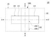
도 1을 참조하면, 반도체장치(100)는 매립게이트구조(100G), 제1불순물영역(113) 및 제2불순물영역(114)을 포함할 수 있다. 기판(101)에 소자분리층(102) 및 활성영역(104)이 형성될 수 있다. 활성영역(104) 내에 제1불순물영역(113) 및 제2불순물영역(114)이 배치될 수 있다. 활성영역(104)과 소자분리층(102)을 가로지르는 트렌치, 즉 게이트트렌치(105)가 형성될 수 있다. 게이트트렌치(105) 내에 매립게이트구조(100G)가 형성될 수 있다. 게이트트렌치(105)에 의해 제1불순물영역(113)과 제2불순물영역(114) 사이에 채널(115)이 형성될 수 있다.Referring to FIG. 1 , the
반도체장치(100)는 트랜지스터를 포함할 수 있다. 이하, 실시예들 및 그 변형예들은, 비-플라나 트랜지스터(Non-planar transistor), 예컨대, 매립게이트형 트랜지스터(Buried gate type transistor)에 적용될 수 있다.The
제1실시예에 따른 반도체장치(100)를 자세히 살펴보기로 한다.The
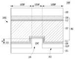
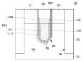
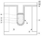
도 2a 및 도 2b는 제1실시예에 따른 반도체장치를 도시한 도면이다. 도 2a는 도 1의 A-A'선에 따른 단면도이다. 도 2b는 도 1의 B-B'선에 따른 단면도이다.2A and 2B are diagrams illustrating a semiconductor device according to the first embodiment. FIG. 2A is a cross-sectional view taken along line A-A' of FIG. 1 . FIG. 2B is a cross-sectional view taken along line B-B' of FIG. 1 .
반도체장치(100)는 기판(101)에 형성된다. 기판(101)은 반도체프로세싱에 적합한 물질일 수 있다. 기판(101)은 반도체기판을 포함할 수 있다. 기판(101)은 실리콘을 함유하는 물질로 이루어질 수 있다. 기판(101)은 실리콘, 단결정 실리콘, 폴리실리콘, 비정질 실리콘, 실리콘저마늄, 단결정 실리콘저마늄, 다결정 실리콘저마늄, 탄소 도핑된 실리콘, 그들의 조합 또는 그들의 다층을 포함할 수 있다. 기판(101)은 저마늄과 같은 다른 반도체물질을 포함할 수도 있다. 기판(101)은 Ⅲ/Ⅴ족 반도체기판, 예컨대 GaAs과 같은 화합물반도체기판을 포함할 수도 있다. 기판(101)은 SOI(Silicon On Insulator) 기판을 포함할 수도 있다.The
기판(101)에 소자분리층(102) 및 활성영역(104)이 형성될 수 있다. 소자분리층(102)에 의해 활성영역(104)이 정의될 수 있다. 소자분리층(102)은 트렌치 식각에 의해 형성된 STI 영역(Shallow Trench Isolation region)일 수 있다. 소자분리층(102)은 얕은 트렌치, 예들 들어, 분리트렌치(Isolation trench, 103)에 절연물질을 채워 형성할 수 있다.A
기판(101) 내에 게이트트렌치(105)가 형성될 수 있다. 평면도로 볼 때, 게이트트렌치(105)는 어느 한 방향으로 연장된 라인 형태(line shaped)가 될 수 있다. 게이트트렌치(105)는 활성영역(104)과 소자분리층(102)을 가로지르는 형태일 수 있다. 게이트트렌치(105)는 분리트렌치(103)보다 더 얕은 깊이를 가질 수 있다. 게이트트렌치(105)는 제1트렌치(105A)와 제2트렌치(105B)를 포함할 수 있다. 제1트렌치(105A)는 활성영역(104) 내에 형성될 수 있다. 제2트렌치(105B)는 소자분리층(102) 내에 형성될 수 있다. 제1트렌치(105A)로부터 제2트렌치(105B)로 연속적으로 확장될 수 있다. 제1트렌치(105A)의 바닥면과 제2트렌치(105B)의 바닥면은 동일 레벨에 위치할 수 있다. 게이트트렌치(105)의 저부는 곡률을 가질 수 있다.A
활성영역(104) 내에 제1불순물영역(113)과 제2불순물영역(114)이 형성될 수 있다. 제1불순물영역(113)과 제2불순물영역(114)은 도전형 불순물이 도핑된 영역이다. 예컨대, 도전형 불순물은 인(P), 비소(As), 안티몬(Sb) 또는 붕소(B)를 포함할 수 있다. 제1불순물영역(113)과 제2불순물영역(114)은 동일 도전형의 불순물로 도핑될 수 있다. 게이트트렌치(105) 양측의 활성영역(104) 내에 제1불순물영역(113)과 제2불순물영역(114)이 위치한다. 제1불순물영역(113)과 제2불순물영역(114)은 각각 소스영역과 드레인영역이라고 지칭될 수 있다. 제1불순물영역(113)과 제2불순물영역(114)의 하부면은 활성영역(104)의 상부 표면(top surface)으로부터 소정의 깊이에 위치할 수 있다. 제1불순물영역(113)과 제2불순물영역(114)은 게이트트렌치(105)의 측벽에 접할 수 있다. 제1불순물영역(113)과 제2불순물영역(114)의 하부면은 게이트트렌치(105)의 바닥면보다 높을 수 있다.A
게이트트렌치(105) 내에 매립게이트구조(100G)가 내장될 수 있다. 매립게이트구조(100G)는 제1불순물영역(113)과 제2불순물영역(114) 사이의 활성영역(104) 내에 배치되면서 소자분리층(102) 내로 연장될 수 있다. 매립게이트구조(100G)는 활성영역(104) 내에 배치된 부분의 바닥면과 소자분리층(102) 내에 배치된 부분의 바닥면이 동일 레벨에 위치할 수 있다.A buried
매립게이트구조(100G)는 게이트절연층(106), 게이트전극(BG), 일함수조절라이너(work function adjusting liner, 110), 캡핑층(109)을 포함할 수 있다. 게이트전극(BG)은 활성영역(104)의 상부면보다 낮은 레벨에 위치할 수 있다. 게이트전극(BG)은 게이트트렌치(105)를 부분적으로 채울 수 있다. 따라서, '매립 게이트전극'이라고 지칭될 수 있다. 캡핑층(109)은 게이트전극(BG) 상에 위치할 수 있다. 게이트절연층(106)은 게이트트렌치(105)의 바닥면 및 측벽들 상에 형성될 수 있다. 일함수조절라이너(110)는 게이트전극(BG)과 게이트절연층(106) 사이에 위치할 수 있다.The buried
게이트절연층(106)은 실리콘산화물(Silicon oxide), 실리콘질화물(Silicon nitride), 실리콘산질화물(Silicon oxynitride), 고유전물질(High-k material) 또는 이들의 조합을 포함할 수 있다. 고유전물질은 실리콘산화물의 유전상수(dielectric constant)보다 더 큰 유전상수를 갖는 물질을 포함할 수 있다. 예컨대, 고유전물질은 3.9보다 큰 유전상수를 갖는 물질을 포함할 수 있다. 다른 예에서, 고유전물질은 10보다 큰 유전상수를 갖는 물질을 포함할 수 있다. 또다른 예에서, 고유전물질은 10 내지 30의 유전상수를 갖는 물질을 포함할 수 있다. 고유전물질은 적어도 하나의 금속성 원소(at least one metallic element)를 포함할 수 있다. 고유전물질은 하프늄함유물질(hafnium-containing material)을 포함할 수 있다. 하프늄함유물질은 하프늄산화물(hafnium oxide), 하프늄실리콘산화물(hafnium silicon oxide), 하프늄실리콘산화질화물(hafnium silicon oxynitride) 또는 그들의 조합을 포함할 수 있다. 다른 실시예에서, 고유전물질은 란탄산화물(lanthanum oxide), 란탄알루미늄산화물(lanthanum aluminum oxide), 지르코늄산화물(zirconium oxide), 지르코늄실리콘산화물(zirconium silicon oxide), 지르코늄실리콘산화질화물(zirconium silicon oxynitride), 알루미늄산화물(aluminum oxide), 및 그들의 조합을 포함할 수 있다. 고유전물질로는 공지된 다른 고유전물질이 선택적으로 사용될 수도 있다. 게이트절연층(106)은 일함수조절라이너(110)에 따라 적절한 물질이 선택될 수 있다. 예컨대, 게이트절연층(106)은 일함수조절라이너(110)보다 단위부피당 산소함량이 작은 물질이 선택될 수 있다.The
제1불순물영역(113)과 제2불순물영역(114) 사이의 게이트전극(BG)을 따라 채널(115)이 형성될 수 있다. 채널(115)은 일반적인 플라나형 트랜지스터(Planar type transistor)에 비해 채널길이가 길다. 이에 따라, 숏채널효과를 방지할 수 있다.A
게이트전극(BG)은 하부 매립부(Lower buried portion, 107)와 상부 매립부(108)를 포함할 수 있다. 하부 매립부(107) 상에 상부 매립부(108)가 위치할 수 있고, 상부 매립부(108)는 제1불순물영역(113) 및 제2불순물영역(114)과 오버랩될 수 있다. 상부 매립부(108)는 하부 매립부(107) 상에서 게이트트렌치(105)에 부분적으로 채워진다. 상부 매립부(108)의 상부 표면 높이는 기판(101)의 상부 표면보다 낮은 레벨일 수 있다. 상부 매립부(108)는 게이트절연층(106)을 사이에 두고 제1,2불순물영역(113, 114)과 오버랩될 수 있다. 즉, 제1,2불순물영역(113, 114)은 상부 매립부(108)와 오버랩되는 깊이를 가질 수 있다.The gate electrode BG may include a lower buried
상부 매립부(108)의 상부에 캡핑층(109)이 채워질 수 있다. 캡핑층(109)은 게이트전극(BG)을 보호하는 역할을 한다. 캡핑층(109)은 절연물질을 포함할 수 있다. 캡핑층(109)는 실리콘질화물, 실리콘산화질화물 또는 이들의 조합을 포함할 수 있다. 다른 실시예에서, 캡핑층(109)은 실리콘질화물과 실리콘산화물의 조합을 포함할 수 있다. 예컨대, 캡핑층(109)을 형성하기 위해 실리콘질화물로 라이닝한 후, 스핀온절연물질(Spin On Dielectric; SOD)로 채울 수 있다.A
게이트전극(BG) 및 일함수조절라이너(110)에 대해 자세히 살펴보면 다음과 같다.The gate electrode BG and the work
일함수조절라이너(110)는 일함수를 조절하기 위한 물질로서, 예컨대, 하부 매립부(107)의 유효일함수(Effective Work function)를 조절하기 위한 물질일 수 있다. 일함수조절라이너(110)에 의해 하부 매립부(107)와 게이트절연층(106) 사이에 증가된 유효일함수, 즉 고일함수(High workfunction)를 발현할 수 있다. 여기서, 고일함수란 실리콘의 미드갭일함수(Mid-gap Work Function)보다 높은 일함수를 지칭한다. 저일함수는 실리콘의 미드갭일함수보다 낮은 일함수를 지칭한다. 부연 설명하면, 고일함수는 4.5eV보다 높은 일함수를 갖고, 저일함수는 4.5eV보다 낮은 일함수를 가질 수 있다. 일함수조절라이너(110)는 게이트절연층(106)과 하부 매립부(107) 사이에 다이폴(dipole)을 생성하여(generated) 에너지밴드(Energy band) 변화로 인한 고일함수 특성을 유도하는 물질을 포함할 수 있다. 일함수조절라이너(110)와 게이트절연층(106)는 서로 다른 산소함량을 가질 수 있다. 일함수조절라이너(110)는 게이트절연층(106)보다 단위부피당 산소함량이 큰 고산소함유-금속산화물(High oxygen contained-metal oxide)로 형성할 수 있다. 게이트절연층(106)이 SiO2인 경우, 일함수조절라이너(110)는 알루미늄산화물(Al2O3), 티타늄산화물(TiO2), 하프늄산화물(HfO2), 지르코늄산화물(ZrO2) 또는 마그네슘산화물(MgO)을 포함할 수 있다. 본 실시예에서, 일함수조절라이너(110)는 알루미늄산화물(Al2O3)을 포함할 수 있다. 알루미늄산화물은 다른 고산소함유-금속산화물보다 산소함량이 더 크다. 따라서, 문턱전압 쉬프트가 더 크게 일어난다. 일함수조절라이너(110)로서 알루미늄산화물(Al2O3)을 적용함에 따라, 게이트절연층(106)과 상호 안정적인 계면 상태를 유지할 수 있다. 일함수조절라이너(110)는 얇은 두께로 형성될 수 있다. 이로써, 게이트트렌치(105) 내에서의 하부 매립부(107)의 체적을 크게 하여 게이트전극(BG)의 저항을 현저히 낮출 수 있다.The work
게이트전극(BG)의 하부 매립부(107)와 상부 매립부(108)는 불연속될 수 있다. 예를 들어, 하부 매립부(107)와 상부 매립부(108)는 서로 다른 물질일 수 있다. 게이트전극(BG)의 상부 매립부(108)는 제1일함수를 가질 수 있다. 여기서, 제1일함수는 실리콘의 미드갭 일함수(mid-gap work function)보다 낮은 일함수값을 지칭할 수 있다. 예컨대, 제1일함수는 4.5eV보다 낮은 저일함수(Low workfunction)를 가질 수 있다. 상부 매립부(108)는 비-금속물질(Non-metal material)을 포함할 수 있다. 상부 매립부(108)는 N형 도펀트(N-type dopant)가 함유된 실리콘함유물질을 포함할 수 있다. 본 실시예에서, 상부 매립부(108)는 N형 도펀트가 도핑된 폴리실리콘(이하, N형 도프드 폴리실리콘)을 포함할 수 있다. N형 도프드 폴리실리콘은 저일함수(Low work function)를 갖는다. N형 도펀트는 인(Ph) 또는 비소(As)를 포함할 수 있다. 상부 매립부(108)는 제1불순물영역(113)과 제2불순물영역(114)에 오버랩(overlap)될 수 있다. 예컨대, 상부 매립부(108)는 제1불순물영역(113)과 제2불순물영역(114)에 수평적으로 오버랩될 수 있다. 일함수조절라이너(110)에 의해 하부 매립부(107)와 게이트절연층(106) 사이에 상부 매립부(108)의 제1일함수보다 높은 제2일함수가 유도될 수 있다. 예를 들어, 제2일함수는 고일함수일 수 있다. 다른 실시예에서, 하부 매립부(107)가 제1고일함수를 갖는 물질로 형성되는 경우, 일함수조절라이너(110)에 의해 하부 매립부(107)와 게이트절연층(106) 사이에 제1고일함수보다 더 높은 제2고일함수가 유도될 수 있다.The lower buried
게이트전극(BG)의 하부 매립부(107)는 게이트전극(BG)의 저항을 낮추기 위해 저저항금속을 포함할 수 있다. 하부 매립부(107)는 상부 매립부(108)보다 낮은 비저항 물질을 포함할 수 있다. 제1실시예에서, 하부 매립부(107)는 상부 매립부(108)에 대해 반응성물질(reactive materials)로 형성될 수 있다. 즉, 상부 매립부(108)와 반응하기 쉬운 물질로 형성될 수 있다. 예를 들어, 하부 매립부(107)로서 텅스텐(W)이 사용될 수 있다. 하부 매립부(107)의 텅스텐과 상부 매립부(108)의 실리콘이 반응하여 텅스텐실리사이드가 형성될 수 있다. 텅스텐실리사이드에 의해 저항이 증가될 수 있다. 따라서, 이러한 실리사이드 반응을 방지하기 위해, 하부 매립부(107)와 상부 매립부(108) 사이에 중간배리어(middle barrier, 112)가 형성될 수 있다.The lower buried
위와 같이, 하부 매립부(107)는 상부 매립부(108)보다 비저항이 낮고, 상부 매립부(108)에 대해 반응성물질인 저저항 금속으로 형성될 수 있다. 하부 매립부(107)로서 텅스텐이 사용되는 경우, 게이트절연층(106)에 어택을 줄 수 있다. 예컨대, 텅스텐은 육불화텅스텐(WF6) 가스를 이용하여 증착할 수 있고, 이때 불소(Fluorine)에 의해 게이트절연층(106)이 어택받을 수 있다. 따라서, 불소 어택을 방지하기 위해 하부 매립부(107)와 게이트절연층(106) 사이에 하부 배리어(Lower barrier, 111)가 형성될 수 있다. 하부 배리어(111)는 하부 매립부(107)와 일함수조절라이너(110) 사이에 위치할 수 있다. 하부 배리어(111)는 비저항이 낮은 물질로 형성될 수 있다. 일부 실시예에서, 불소가 미함유된 텅스텐소스에 의해 텅스텐층을 증착하는 경우, 하부 배리어(111)는 생략될 수 있다.As described above, the lower buried
제1불순물영역(113), 제2불순물영역(114) 및 매립게이트구조(100G)는 트랜지스터를 구성할 수 있다. 예컨대, 트랜지스터는 '매립게이트형 트랜지스터(Buried Gate type transistor)'라고 지칭할 수 있다. 제1불순물영역(113)과 제2불순물영역(114) 사이의 게이트트렌치(105)의 표면을 따라 채널(115)이 정의될 수 있다. 일부 실시예에서, 채널(115)은 채널도핑(channel doping)에 의한 도펀트를 포함할 수 있다.The
제1실시예에 따르면, 일함수조절라이너(110)는 고일함수를 유도하는 물질이고, 상부 매립부(108)는 저일함수를 갖는 물질이다.According to the first embodiment, the work
일함수조절라이너(110)에 의해 문턱전압(Threshold voltage, Vt)이 조절된다. 예컨대, 일함수조절라이너(110)에 의해 문턱전압을 쉬프트(Shift)시킬 수 있다. 일함수조절라이너(110)에 의해 일함수조절라이너(110)와 게이트절연층(106)의 계면에 다이폴(dipole)을 형성시킨다. 다이폴은 일함수조절라이너(110)와 게이트절연층(106)간의 산소함량 차이에 의해 발생될 수 있다. 이러한 다이폴은 하부 매립부(107)와 게이트절연층(106) 사이에 고일함수를 유도하고, 이에 따라 문턱전압을 쉬프트시킬 수 있다. 결국, 일함수조절라이너(110)에 의해 채널(115)의 도즈(channel dose)를 낮출 수 있다. 일함수조절라이너(110)와 게이트절연층(106) 사이에 생성되는 다이폴의 극성 방향(polarity direction)을 제어하므로써 게이트전극(BG)의 일함수를 제어할 수 있다. 이러한 방법에 의해, 게이트전극(BG)의 하부매립부(107)의 일함수는 증가 또는 감소될 수 있다. 예컨대, 일함수조절라이너(110)가 게이트절연층(106)보다 단위부피당 산소함량이 큰 물질인 경우, 고일함수로 변화시키는 방향의 다이폴이 생성될 수 있다. 일함수조절라이너(110)가 게이트절연층(106)보다 단위부피당 산소함량이 작은 물질인 경우, 저일함수로 변화시키는 방향의 다이폴이 생성될 수 있다. 본 실시예에서, 일함수조절라이너(110)는 게이트절연층(106)보다 단위부피당 산소함량이 큰 물질이므로, 게이트절연층(106)과의 계면에 고일함수로 변화시키는 방향의 다이폴이 생성될 수 있다. 게이트절연층(106)이 SiO2인 경우, SiO2보다 단위부피당 산소함량이 큰 물질은 알루미늄산화물(Al2O3), 티타늄산화물(TiO2), 하프늄산화물(HfO2), 지르코늄산화물(ZrO2) 또는 마그네슘산화물(MgO)을 포함할 수 있다. SiO2보다 단위부피당 산소함량이 작은 물질은 이트륨산화물(Y2O3), 란탄늄산화물(La2O3), 저마늄산화물(GeO2), 루테튬산화물(Lu2O3) 또는 스트론튬산화물(SrO)을 포함할 수 있다. 예를 들어, SiO2에 대한 Al2O3의 단위부피당 산소함량비(

게이트트렌치(105)가 고종횡비(High aspect ratio)를 갖기 때문에, 일반적인 채널도핑에 의해서는, 게이트트렌치(105)의 바닥부까지 충분히 도핑을 수행하기 어렵다. 따라서, 채널도핑 이후에 추가로 게이트트렌치(105)의 바닥부에 국부적으로 채널도핑을 수행하는데, 이를 '국부적채널도핑'이라 지칭한다. 국부적채널도핑으로서 임플란트(Implantation)를 적용하는 경우, LCI(Locally Channel Implantation)라고 지칭한다.Since the
일함수조절라이너(110)에 의해 채널 도즈를 낮출 수 있으므로, 국부적채널도핑(LCI)의 도즈를 현저히 낮추거나, 국부적채널도핑(LCI)을 생략할 수 있다. 결국, 본 실시예들은, 채널도즈를 낮추므로, 접합누설(junction leakage) 특성이 개선된다.Since the channel dose can be lowered by the work
또한, 제1실시예는, 상부 매립부(108)가 저일함수를 갖기 때문에, 제1불순물영역(113) 및 제2불순물영역(114)에서의 게이트유도드레인누설(GIDL)을 억제할 수 있다. 일함수조절라이너(110)가 제1불순물영역(113) 및 제2불순물영역(114)에 오버랩되는 경우, 고일함수 유도로 인해 게이트유도드레인누설이 증가될 수 있다. 따라서, 일함수조절라이너(110)는 제1불순물영역(113) 및 제2불순물영역(114)에 비-오버랩(Non-overlap)되도록 높이가 조절될 수 있다.In addition, in the first embodiment, since the upper buried
상부 매립부(108)의 비저항이 다른 금속물질들에 비해 상대적으로 높을 수 있으나, 게이트전극(BG)에서 차지하는 상부 매립부(108)의 비율(즉, 두께)을 최대한 작게(즉, 얇게) 하므로써 게이트전극(BG)의 저항에 미치는 영향은 무시할 수 있다.Although the resistivity of the upper buried
한편, 비교예로서, 상부 매립부(108)로서, 저일함수 금속물질, 즉 N형 일함수 금속이 사용될 수도 있으나, N형 일함수 금속은 N형 도프드 폴리실리콘의 일함수보다 높다. N형 일함수 금속으로는 N형 도프드 폴리실리콘에 준하는 낮은 일함수를 얻기 어렵다. 또한, 일함수조절라이너(110)로서 'TiAlN'과 같은 고일함수의 도전성 물질이 사용될 수 있으나, TiAlN은 텅스텐(W)보다 저항이 큰 물질이므로 절연성의 일함수조절라이너(110), 즉 Al2O3를 적용하는 경우보다 게이트전극(BG)의 저항을 낮추는데 한계가 있다. 아울러, TiAlN은 Al2O3를 적용하는 경우보다 다이폴 밀도가 미약하여 문턱전압 쉬프트 효과가 크지 않다.Meanwhile, as a comparative example, as the upper buried
제1실시예에 따른 매립게이트구조(100G)는 매립게이트형 핀채널 트랜지스터(Buried Gate type Fin channel transistor)에 적용될 수 있다.The buried
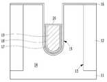
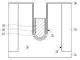
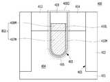
도 3a 및 도 3b는 제1실시예가 적용된 매립 게이트형 핀채널 트랜지스터를 도시한 도면이다. 도 3a는 도 1의 A-A'선에 따른 단면도이다. 도 3b는 도 1의 B-B'선에 따른 단면도이다. 반도체장치(100F)의 일부 구성들은 제1실시예의 반도체장치(100)와 동일할 수 있다.3A and 3B are diagrams illustrating a buried gate type fin channel transistor to which the first embodiment is applied. 3A is a cross-sectional view taken along line A-A' of FIG. 1 . 3B is a cross-sectional view taken along line B-B' of FIG. 1 . Some configurations of the
도 3a 및 도 3b를 참조하면, 게이트트렌치(105)는 제1트렌치(105AF)와 제2트렌치(105BF)를 포함한다. 제1트렌치(105AF)는 활성영역(104) 내에 형성된다. 제2트렌치(105BF)는 소자분리층(102) 내에 형성된다. 제1트렌치(105AF)로부터 제2트렌치(105BF)로 연속적으로 연장될 수 있다. 게이트트렌치(105)에서, 제1트렌치(105AF)와 제2트렌치(105BF)는 서로 다른 레벨에 위치하는 바닥면을 가질 수 있다. 예를 들어, 제1트렌치(105AF)의 바닥면은 제2트렌치(105BF)의 바닥면보다 높은 레벨에 위치할 수 있다. 제1트렌치(105AF)와 제2트렌치(105BF)의 높이 차이는 소자분리층(102)이 리세스됨에 따라 형성된다. 따라서, 제2트렌치(105BF)는 제1트렌치(105AF)의 바닥면보다 낮은 바닥면을 갖는 리세스영역(R)을 포함할 수 있다.3A and 3B , the
제1트렌치(105AF)와 제2트렌치(105BF) 사이의 단차로 인하여 활성영역(104)에 핀(Fin, 104F)이 형성된다. 따라서, 활성영역(104)은 핀(104F)을 포함한다.A
이와 같이, 제1트렌치(105AF) 아래에 핀(104F)이 형성되고, 핀(104F)의 측벽은 리세스된 소자분리층(102F)에 의해 노출된다. 핀(104F)은 채널이 형성되는 부분이다. 핀(104F)은 새들핀(Saddle Fin)이라고 일컫는다. 핀(104F)에 의해 채널 폭을 증가시킬 수 있고, 전기적 특성을 향상시킬 수 있다.In this way, a
반도체장치(100F)의 매립게이트구조(100G)는 게이트절연층(106), 일함수조절라이너(110), 게이트전극(BG) 및 캡핑층(109)을 포함할 수 있다. 핀(104F)의 측벽과 상부 표면 상에 게이트절연층(106)이 형성된다. 일함수조절라이너(110) 및 하부 매립부(107)는 핀(104F)의 측벽과 상부를 모두 덮는 형태가 된다. 하부 매립부(107)는 리세스영역(R)을 채우면서 게이트트렌치(105) 내에 형성된다. 하부 매립부(107)의 단면적은 활성영역(104) 내에서보다 소자분리층(102) 내에서 더 넓을 수 있다. 상부 매립부(108)는 핀(104F)의 측벽 주변에 위치하지 않는다. 핀(104F)의 채널도즈는 일함수조절라이너(110)에 의해 영향을 받는다.The buried
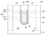
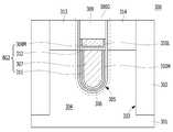
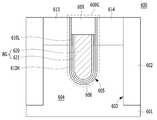
도 4는 제1실시예의 변형예에 따른 반도체장치를 도시한 도면이다. 반도체장치(100M)의 일부 구성들은 제1실시예의 반도체장치(100)와 동일할 수 있다.4 is a diagram showing a semiconductor device according to a modification of the first embodiment. Some configurations of the
반도체장치(100M)의 매립게이트구조(100GM)는 게이트절연층(106), 일함수조절라이너(110), 게이트전극(BGM) 및 캡핑층(109)을 포함할 수 있다.The buried gate structure 100GM of the
게이트전극(BGM)은 하부 매립부(107M)와 상부 매립부(108)를 포함할 수 있다. 하부 매립부(107M)는 채널(115)과 오버랩될 수 있고, 상부 매립부(108)는 제1불순물영역(113) 및 제2불순물영역(114)과 오버랩될 수 있다.The gate electrode BGM may include a lower buried
게이트전극(BGM)의 하부 매립부(107M)는 게이트전극(BGM)의 저항을 낮추기 위해 저저항금속을 포함할 수 있다. 하부 매립부(107M)는 상부 매립부(108)보다 낮은 비저항 물질을 포함할 수 있다. 하부 매립부(107M)는 상부 매립부(108)에 대해 비-반응성물질(Non-reactive materials)로 형성될 수 있다. 즉, 상부 매립부(108)와 반응하지 않는 물질로 형성될 수 있다. 예를 들어, 하부 매립부(108M)로서 티타늄질화물이 사용되는 경우, 상부 매립부(108)의 실리콘과 하부 매립부(107M)는 반응하지 않는다. 따라서, 하부 매립부(107M)와 상부 매립부(108) 사이에 중간배리어가 생략될 수 있다.The lower buried
위와 같이, 하부 매립부(107M)는 상부 매립부(108)보다 비저항이 낮고, 상부 매립부(108)에 대해 비-반응성물질인 저저항 금속으로 형성될 수 있다.As described above, the lower buried
아울러, 하부 매립부(107M)는 게이트절연층(106)에 어택을 주지 않는 물질로 형성될 수 있다. 예컨대, 하부 매립부(107M)는 불소(Fluorine)와 같은 불순물이 미함유된 물질(Fluorine-free material)로 형성될 수 있다. 따라서, 하부 매립부(107M)와 게이트절연층(106) 사이에 하부 배리어가 생략될 수 있다.In addition, the lower buried
하부 매립부(107M)는 티타늄질화물을 포함할 수 있다. 하부 매립부(107M)가 상부 매립부(108)에 대해 비-반응성물질이면서 불소미함유물질이므로, 게이트전극(BGM)은 배리어가 필요없게 되어, '배리어-리스 게이트전극(barrier-less gate electrode)'이라고 지칭할 수 있다.The lower buried
도 4의 매립게이트구조(100M)는 도 3a 및 도 3b와 같은 매립게이트형 핀채널 트랜지스터에 적용될 수도 있다.The buried
이하, 제1실시예에 따른 반도체장치의 제조 방법이 설명된다.Hereinafter, a method of manufacturing the semiconductor device according to the first embodiment will be described.
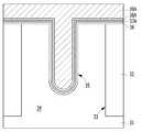
도 5a 내지 도 5g는 제1실시예에 따른 반도체장치를 제조하는 방법의 일예를 설명하기 위한 도면이다. 도 5a 내지 도 5g는 도 1의 A-A'선에 따른 공정 단면도이다.5A to 5G are diagrams for explaining an example of a method of manufacturing the semiconductor device according to the first embodiment. 5A to 5G are cross-sectional views taken along line A-A' of FIG. 1 .
도 5a에 도시된 바와 같이, 기판(11)에 소자분리층(12)이 형성된다. 소자분리층(12)에 의해 활성영역(14)이 정의된다. 소자분리층(12)은 STI 공정에 의해 형성될 수 있다. 예를 들어, 기판(11) 상에 패드층(Pad layer, 도시 생략)을 형성한 후 소자분리마스크(도시 생략)를 이용하여 패드층 및 기판(11)을 식각한다. 이로써 분리트렌치(13)가 형성된다. 분리트렌치(13)는 절연물질로 채워지고, 이에 따라 소자분리층(12)이 형성된다. 소자분리층(12)은 실리콘산화물, 실리콘질화물 또는 이들의 조합을 포함할 수 있다. 화학기상증착(CVD) 또는 다른 증착공정은 절연물질로 분리트렌치(13)를 채우는데 사용될 수 있다. CMP(chemical-mechanical polishing)와 같은 평탄화 공정(planarization process)이 부가적으로 사용될 수 있다.As shown in FIG. 5A , the
기판(11) 내에 게이트트렌치(15)가 형성된다. 게이트트렌치(15)는 활성영역(14) 및 소자분리층(12)을 가로지르는 라인 형태로 형성될 수 있다. 게이트트렌치(15)는 기판(11) 상에 마스크패턴(도시 생략)을 형성하고, 마스크 패턴을 식각 마스크로 이용한 식각 공정에 의해 형성될 수 있다. 게이트트렌치(15)는 분리트렌치(13)보다 얕게 형성될 수 있다. 게이트트렌치(15)의 깊이는 후속 게이트전극의 평균 단면적을 크게 할 수 있는 충분한 깊이를 가질 수 있다. 이에 따라, 게이트전극의 저항을 감소시킬 수 있다. 게이트트렌치(15)의 저부는 곡률을 가질 수 있다. 이와 같이 곡률을 갖도록 형성하므로써, 게이트트렌치(15)의 저부에서 요철을 최소화하고, 그에 따라 게이트전극의 채움(filling)을 용이하게 수행할 수 있다. 또한, 곡률을 갖도록 하므로써, 게이트트렌치(15)의 저부 모서리에 각진 모양을 제거하여 전계집중(electric field)을 완화할 수 있다.A
도 5b에 도시된 바와 같이, 게이트트렌치(15)의 표면 상에 게이트절연층(16)이 형성될 수 있다. 게이트절연층(16)을 형성하기 전에, 게이트트렌치(15) 표면의 식각손상을 치유할 수 있다. 예컨대, 열산화 처리에 의해 희생산화물을 형성한 후, 희생산화물을 제거할 수 있다.As shown in FIG. 5B , a
게이트절연층(16)은 열산화 공정(Thermal Oxidation)에 의해 형성될 수 있다. 다른 실시예에서, 게이트절연층(16)은 화학기상증착(Chemical Vapor Deposition; CVD) 또는 원자층증착(Atomic Layer Deposition; ALD)에 의해 형성될 수 있다. 게이트절연층(16)은 고유전물질, 산화물, 질화물, 산화 질화물 또는 이들의 조합을 포함할 수 있다. 고유전물질은 하프늄함유물질을 포함할 수 있다. 하프늄함유물질은 하프늄산화물, 하프늄실리콘산화물, 하프늄실리콘산화질화물 또는 그들의 조합을 포함할 수 있다. 다른 실시예에서, 고유전물질은 란탄산화물, 란탄알루미늄산화물, 지르코늄산화물, 지르코늄실리콘산화물, 지르코늄실리콘산화질화물, 알루미늄산화물 및 그들의 조합을 포함할 수 있다. 고유전물질로는 공지된 다른 고유전물질이 선택적으로 사용될 수도 있다.The
게이트절연층(16) 상에 일함수조절라이너층(17A)이 형성될 수 있다. 일함수조절라이너층(17A)은 게이트절연층(16)의 표면 상에 컨포멀하게 형성될 수 있다. 일함수조절라이너층(17A)은 일함수를 조절하기 위한 물질이다. 일함수조절라이너층(17A)은 게이트절연층(16)과의 계면에 다이폴(dipole)을 생성하여(generated) 에너지밴드 변화로 인한 고일함수 특성을 유도하는 물질을 포함할 수 있다. 일함수조절라이너층(17A)은 SiO2보다 단위부피당 산소함량이 큰 물질로 형성될 수 있다. 알루미늄산화물(Al2O3), 티타늄산화물(TiO2), 하프늄산화물(HfO2), 지르코늄산화물(ZrO2) 또는 마그네슘산화물(MgO)을 포함할 수 있다. 본 실시예에서, 일함수조절라이너층(17A)은 Al2O3를 포함할 수 있다. 일함수조절라이너층(17A)으로서 알루미늄산화물을 적용함에 따라, 게이트절연층(16)과 상호 안정적인 계면 상태를 유지할 수 있다. 일함수조절라이너층(17A)은 얇은 두께로 형성될 수 있다.A work function
일함수조절라이너층(17A) 상에 제1저저항층(19A)이 형성될 수 있다. 제1저저항층(19A)은 게이트트렌치(15)를 채울 수 있다. 제1저저항층(19A)은 저저항 금속물질을 포함한다. 제1저저항층(19A)은 후속 일함수라이너층에 대해 반응성물질(reactive material)로 형성될 수 있다. 제1저저항층(19A)은 텅스텐을 포함할 수 있다. 텅스텐이 불소를 함유하는 경우, 제1저저항층(19A)을 형성하기 전에 하부 배리어층(18A)을 미리 형성할 수 있다. 하부 배리어층(18A)은 일함수조절라이너층(17A)의 표면 상에 컨포멀하게 형성될 수 있다. 하부 배리어층(18A)은 금속함유물질로 형성될 수 있다. 하부 배리어층(18A)은 금속질화물(Metal nitride)을 포함할 수 있다. 예를 들어, 하부 배리어층(18A)은 티타늄질화물(Titanium nitride)을 포함할 수 있다. 하부 배리어층(18A)은 후속 리세싱 공정에 의해 하부 배리어가 될 수 있다. 다른 실시예로서, 제1저저항층(19A)은 게이트절연층(16)의 어택을 방지하기 위해, 불소와 같은 불순물들을 미함유하는 물질로 형성될 수 있다. 아울러, 제1저저항층(19A)은 후속 일함수라이너층에 대해 비-반응성물질(Non-reactive material)로 형성될 수 있다. 다른 실시예에서, 제1저저항층(19A)은 티타늄질화물로 형성될 수 있다. 제1저저항층(19A)은 화학기상증착법(CVD) 또는 원자층증착법(ALD)에 의해 형성될 수 있다.A first
도 5c에 도시된 바와 같이, 게이트트렌치(15) 내부에 하부 매립부(19)가 잔류하도록 제1리세싱 공정(first recessing process)을 진행한다. 제1리세싱 공정은 건식식각, 예컨대, 에치백공정에 의해 진행될 수 있다. 제1일함수라이너(17)는 제1일함수라이너층(17A)의 에치백공정에 의해 형성된다. 하부 매립부(19)는 제1저저항층(19A)의 에치백공정에 의해 형성된다. 다른 실시예에서, 제1리세싱 공정은 평탄화 공정을 먼저 진행한 후에, 후속하여 에치백 공정을 진행할 수 있다. 제1리세싱 공정에 의해 하부 배리어층도 리세싱될 수 있다. 이에 따라, 하부 배리어(18)가 형성될 수 있다. 하부 배리어(18)는 하부 매립부(19)와 게이트절연층(16) 사이에 위치할 수 있다. 하부 배리어(18)와 하부 매립부(19)의 상부 표면 높이는 동일 레벨일 수 있다.As shown in FIG. 5C , a first recessing process is performed so that the lower buried
상술한 제1리세싱 공정에 의해 하부 매립부(19)가 형성된다. 하부 매립부(19)는 활성영역(14)의 상부 표면보다 낮게 리세스될 수 있다.The lower buried
도 5d에 도시된 바와 같이, 게이트트렌치(15) 내부에 일함수조절라이너(17)가 잔류하도록 제2리세싱 공정(Second recessing process)을 진행한다. 제2리세싱 공정은 건식식각 또는 습식식각에 의해 진행될 수 있다. 일함수조절라이너(17)는 일함수조절라이너층(17A)의 에치백공정에 의해 형성된다. 제2리세싱 공정은 게이트절연층(16)의 어택없이 수행될 수 있다. 일함수조절라이너(17)는 하부 매립부(19)와 게이트절연층(16) 사이에 위치할 수 있다. 일함수조절라이너(17)와 하부 매립부(19) 사이에 하부 배리어(18)가 위치할 수 있다. 일함수조절라이너(17), 하부 배리어(18) 및 하부 매립부(19)의 상부 표면 높이는 동일 레벨일 수 있다.As shown in FIG. 5D , a second recessing process is performed so that the work
도 5e에 도시된 바와 같이, 중간배리어(20)가 형성될 수 있다. 중간배리어(20)는 중간배리어층(도시 생략)을 형성한 후 리세싱공정에 의해 형성될 수 있다. 중간배리어(20)는 하부 배리어(18)과 동일 물질일 수 있다. 중간배리어(20)는 금속함유물질로 형성될 수 있다. 중간배리어(20)는 금속질화물(Metal nitride)을 포함할 수 있다. 예를 들어, 중간배리어(20)는 티타늄질화물(Titanium nitride)을 포함할 수 있다. 중간배리어(20)에 의해 일함수조절라이너(17), 하부 배리어(18) 및 하부 매립부(19)의 상부가 커버링될 수 있다.As shown in FIG. 5E , an
도 5f에 도시된 바와 같이, 상부 매립부(21)가 형성될 수 있다. 상부 매립부(21)는 중간배리어(20) 상에 상부 매립층(21A)을 채운 후에, 제3리세싱 공정에 의해 형성될 수 있다. 상부 매립부(21)는 저일함수 물질을 포함한다. 상부 매립부(21)는 비-금속물질로 형성될 수 있다. 상부 매립부(21)는 N형 불순물이 도핑된 폴리실리콘을 포함할 수 있다. 상부 매립부(21)는 활성영역(14)의 상부 표면보다 낮은 레벨일 수 있다.As shown in FIG. 5F , an upper buried
도 5g에 도시된 바와 같이, 상부 매립부(21) 상에 캡핑층(22)이 형성된다. 캡핑층(22)은 절연물질을 포함한다. 상부 매립부(21) 상에서 게이트트렌치(15)가 캡핑층(22)으로 채워진다. 캡핑층(22)은 실리콘질화물을 포함할 수 있다. 후속하여, 기판(11)의 상부 표면이 노출되도록 캡핑층(22)의 평탄화가 진행될 수 있다. 캡핑층(22)의 평탄화 공정시 또는 평탄화 공정 이후에, 기판(11) 상부 표면의 게이트절연층(16)이 제거될 수 있다.As shown in FIG. 5G , a
상술한 바와 같은 일련의 공정에 의해, 매립게이트구조가 형성된다. 매립게이트구조는 게이트절연층(16), 일함수조절라이너(17), 게이트전극(BG) 및 캡핑층(22)을 포함한다. 게이트전극(BG)은 하부 배리어(18), 하부 매립부(19), 중간배리어(20) 및 상부 매립부(21)를 포함한다. 게이트전극(BG)의 하부 매립부(19)와 게이트절연층(16) 사이에 일함수조절라이너(17)가 위치할 수 있다. 게이트전극(BG)의 상부 표면은 기판(11)의 상부 표면보다 낮게 위치한다. 이와 같이, 게이트전극(BG)의 상부 표면을 낮게 리세스시킴에 따라, 게이트전극(BG)과 주변 도전물(예, 콘택플러그) 간의 물리적 거리를 충분히 확보할 수 있다. 결국, 게이트전극(BG)과 주변 도전물간의 절연 내압을 향상시킬 수 있다.A buried gate structure is formed by a series of processes as described above. The buried gate structure includes a
캡핑층(22) 형성 후에, 임플란트 또는 기타 다른 도핑기술에 의해 불순물의 도핑공정이 수행된다. 이에 따라 기판(11) 내에 제1불순물영역(23)과 제2불순물영역(24)이 형성된다. 불순물의 도핑 공정을 진행할 때, 캡핑층(22)이 배리어로 사용된다. 제1불순물영역(23)과 제2불순물영역(24)은 각각 소스영역과 드레인영역이라고 지칭될 수 있다. 기판(11) 상부 표면의 게이트절연층(16)은 불순물의 도핑 공정 이후에 제거될 수도 있다.After the
제1불순물영역(23)과 제2불순물영역(24)은 상부 매립부(21)와 오버랩되는 깊이를 가질 수 있다. 따라서, 상부 매립부(21)는 제1 및 제2불순물영역(23, 24)에 오버랩될 수 있다.The
다른 실시예에서, 제1불순물영역(23)과 제2불순물영역(24)은 게이트트렌치 (15) 형성전에 형성될 수도 있다. 예컨대, 이온주입마스크를 이용하여 활성영역(14)에 불순물을 도핑하여 불순물영역을 형성한 후, 게이트트렌치(15)를 형성할 수 있다. 이때, 불순물영역이 게이트트렌치(15)에 의해 제1불순물영역(23)과 제2불순물영역(24)으로 분할될 수 있다.In another embodiment, the
도 6은 제2실시예에 따른 반도체장치를 도시한 도면이다. 매립게이트구조(200G)를 제외한 반도체장치(200)의 일부 구성들은 제1실시예의 반도체장치(100)와 동일할 수 있다.6 is a diagram illustrating a semiconductor device according to a second embodiment. Some components of the
반도체장치(200)는 기판(201)에 형성될 수 있다. 반도체장치(200)의 매립게이트구조(200G)는 게이트트렌치(205) 내에 내장될 수 있다. 매립게이트구조(200G)는 제1불순물영역(213)과 제2불순물영역(214) 사이의 활성영역(204) 내에 배치되면서 소자분리층(202) 내로 연장될 수 있다. 소자분리층(202)은 분리트렌치(203)에 절연물질을 채워 형성할 수 있다.The
매립게이트구조(200G)는 게이트절연층(206), 게이트전극(BG), 일함수조절라이너(210H), 캡핑층(209) 및 일함수라이너(work function liner, 210L)를 포함할 수 있다. 게이트전극(BG)은 활성영역(204)의 상부면보다 낮은 레벨에 위치할 수 있다. 게이트전극(BG)은 게이트트렌치(205)를 부분적으로 채울 수 있다. 캡핑층(209)은 게이트전극(BG) 상에 위치할 수 있다. 게이트절연층(206)은 게이트트렌치(205)의 바닥면 및 측벽들 상에 형성될 수 있다. 일함수조절라이너(210)는 게이트전극(BG)과 게이트절연층(206) 사이에 위치할 수 있다.The buried
게이트전극(BG)은 하부 배리어(211B), 하부 매립부(207), 상부 배리어(211T) 및 상부 매립부(208)를 포함할 수 있다. 하부 매립부(207) 상에 상부 매립부(208)가 위치할 수 있고, 상부 매립부(208)는 제1불순물영역(213) 및 제2불순물영역(214)과 오버랩될 수 있다. 상부 매립부(208)는 하부 매립부(207) 상에서 게이트트렌치(205)에 부분적으로 채워진다. 상부 매립부(208)의 상부 표면 높이는 기판(201)의 상부 표면보다 낮은 레벨일 수 있다. 상부 매립부(208)는 게이트절연층(206)을 사이에 두고 제1,2불순물영역(213, 214)과 오버랩될 수 있다. 상부 매립부(208)의 상부에 캡핑층(209)이 채워질 수 있다.The gate electrode BG may include a lower barrier 211B, a lower buried
일함수조절라이너(210H)는 제1실시예에 따른 일함수조절라이너(110)와 동일 물질일 수 있다. 즉, 일함수조절라이너(210H)는 일함수를 조절하기 위한 물질로서, 하부 매립부(207)의 유효일함수를 조절하기 위한 물질일 수 있다. 일함수조절라이너(210H)에 의해 하부 매립부(207)가 증가된 유효일함수, 즉 고일함수를 가질 수 있다. 일함수조절라이너(210H)는 게이트절연층(206)과 하부 매립부(207) 사이에 다이폴을 생성하여 에너지밴드 변화로 인한 고일함수 특성을 유도하는 물질을 포함할 수 있다. 일함수조절라이너(210H)는 게이트절연층(206)보다 단위부피당 산소함량이 큰 고산소함유-금속산화물로 형성할 수 있다. 게이트절연층(206)이 SiO2인 경우, 일함수조절라이너(210H)는 SiO2보다 단위부피당 산소함량이 큰 고산소함유-금속산화물로 형성될 수 있다. 예를 들어, 일함수조절라이너(210H)는 알루미늄산화물(Al2O3), 티타늄산화물(TiO2), 하프늄산화물(HfO2), 지르코늄산화물(ZrO2) 또는 마그네슘산화물(MgO)을 포함할 수 있다. 본 실시예에서, 일함수조절라이너(210H)는 Al2O3를 포함할 수 있다. 일함수조절라이너(210H)로서 알루미늄산화물을 적용함에 따라, 게이트절연층(206)과 상호 안정적인 계면 상태를 유지할 수 있다. 일함수조절라이너(210H)는 Al2O3를 포함할 수 있다. 일함수조절라이너(210H)는 얇은 두께로 형성될 수 있다. 이로써, 게이트트렌치(205) 내에서의 하부 매립부(207)의 체적을 크게 하여 게이트전극(BG)의 저항을 현저히 낮출 수 있다.The work
일함수라이너(210L)는 제1일함수를 가질 수 있다. 여기서, 제1일함수는 실리콘의 미드갭 일함수보다 낮은 일함수값을 지칭할 수 있다. 예컨대, 제1일함수는 4.5eV보다 낮은 저일함수(Low workfunction)를 가질 수 있다. 일함수라이너(210L)는 비-금속물질을 포함할 수 있다. 일함수라이너(210L)는 N형 도펀트가 함유된 실리콘함유물질을 포함할 수 있다. 본 실시예에서, 일함수라이너(210L)는 N형 도펀트가 도핑된 폴리실리콘(이하, N형 도프드 폴리실리콘)을 포함할 수 있다. N형 도프드 폴리실리콘은 저일함수를 갖는다. N형 도펀트는 인(Ph) 또는 비소(As)를 포함할 수 있다. 일함수라이너(210L)는 제1불순물영역(213)과 제2불순물영역(214)에 오버랩될 수 있다. 예컨대, 일함수라이너(210L)는 제1불순물영역(213)과 제2불순물영역(214)에 수평적으로 오버랩될 수 있다. 일함수라이너(210L)는 스페이서 형상일 수 있다. 즉, 일함수라이너(210L)는 상부 매립부(208)와 하부 매립부(207) 사이에 위치하지 않을 수 있다. 일함수라이너(210L)는 상부 매립부(208)와 제1,2불순물영역(213, 214) 사이에 위치할 수 있다. 일함수라이너(210L)와 일함수조절라이너(210H)는 접속될 수 있다. 일함수라이너(210L)와 일함수조절라이너(210H)는 두께가 동일하거나 서로 다를 수 있다. 일함수조절라이너(210H)에 의해 하부 매립부(207)와 게이트절연층(206) 사이에 일함수라이너(210L)의 제1일함수보다 높은 제2일함수가 유도될 수 있다. 예를 들어, 제2일함수는 고일함수일 수 있다. 다른 실시예에서, 하부 매립부(207)가 제1고일함수를 갖는 물질로 형성되는 경우, 일함수조절라이너(210H)에 의해 하부 매립부(207)와 게이트절연층(206) 사이에 제1고일함수보다 더 높은 제2고일함수가 유도될 수 있다.The
게이트전극(BG)의 하부 매립부(207)와 상부 매립부(208)는 게이트전극(BG)의 저항을 낮추기 위해 저저항금속을 포함할 수 있다. 하부 매립부(207)와 상부 매립부(208)는 일함수라이너(210L)보다 낮은 비저항 물질을 포함할 수 있다. 제2실시예에서, 하부 매립부(207) 및 상부 매립부(208)는 일함수라이너(210L)에 대해 반응성물질로 형성될 수 있다. 즉, 일함수라이너(210L)와 반응하기 쉬운 물질로 형성될 수 있다. 예를 들어, 하부 매립부(207) 및 상부 매립부(208)로서 텅스텐(W)이 사용될 수 있다. 상부 매립부(208)의 텅스텐과 일함수라이너(210L)의 실리콘이 반응하여 텅스텐실리사이드가 형성될 수 있다. 텅스텐실리사이드에 의해 저항이 증가될 수 있다. 따라서, 이러한 실리사이드 반응을 방지하기 위해, 상부 매립부(208)와 일함수라이너(210L) 사이에 상부배리어(Upper barrier, 211T)가 형성될 수 있다. 상부 배리어(211T)는 하부 매립부(207)와 상부 매립부(208) 사이에 위치하도록 연장될 수 있다.The lower buried
위와 같이, 하부 매립부(207) 및 상부 매립부(208)는 일함수라이너(210L)보다 비저항이 낮고, 일함수라이너(210L)에 대해 반응성물질인 저저항 금속으로 형성될 수 있다. 하부 매립부(207)로서 텅스텐이 사용되는 경우, 게이트절연층(206)에 어택을 줄수 있다. 예컨대, 텅스텐은 육불화텅스텐(WF6) 가스를 이용하여 증착할 수 있고, 이때 불소에 의해 게이트절연층(206)이 어택받을 수 있다. 따라서, 불소 어택을 방지하기 위해 하부 매립부(207)와 게이트절연층(206) 사이에 하부 배리어(211B)가 형성될 수 있다. 하부 배리어(211B)는 하부 매립부(207)와 일함수조절라이너(210H) 사이에 위치할 수 있다. 하부 배리어(211B)는 비저항이 낮은 물질로 형성될 수 있다. 일부 실시예에서, 불소가 미함유된 텅스텐소스에 의해 텅스텐층을 증착하는 경우, 하부 배리어(211B)는 생략될 수 있다.As described above, the lower buried
제1불순물영역(213), 제2불순물영역(214) 및 매립게이트구조(200G)는 매립게이트형 트랜지스터를 형성할 수 있다. 제1불순물영역(213)과 제2불순물영역(214) 사이의 게이트트렌치(205)의 표면을 따라 채널이 정의될 수 있다.The
제2실시예에 따르면, 일함수조절라이너(210H)는 고일함수를 유도하는 물질이고, 일함수라이너(210L)는 저일함수를 갖는 물질이다.According to the second embodiment, the work
일함수조절라이너(210H)에 의해 문턱전압(Vt)이 조절된다. 예컨대, 일함수조절라이너(210H)에 의해 문턱전압을 쉬프트시킬 수 있다. 일함수조절라이너(210H)에 의해 일함수조절라이너(210H)와 게이트절연층(206)의 계면에 다이폴을 형성시킨다. 다이폴은 하부 매립부(207)과 게이트절연층(206) 사이에 고일함수를 유도하고, 이에 따라 문턱전압을 쉬프트시킬 수 있다. 결국, 일함수조절라이너(210H)에 의해 채널의 도즈를 낮출 수 있다.The threshold voltage Vt is adjusted by the work
일함수조절라이너(210H)에 의해 채널 도즈를 낮출 수 있으므로, 국부적채널도핑의 도즈를 현저히 낮추거나, 국부적채널도핑을 생략할 수 있다. 결국, 본 실시예들은, 채널도즈를 낮추므로, 접합누설 특성이 개선된다.Since the channel dose can be lowered by the work
또한, 제2실시예는, 일함수라이너(210L)가 저일함수를 갖기 때문에, 제1불순물영역(213) 및 제2불순물영역(214)에서의 게이트유도드레인누설(GIDL)을 억제할 수 있다. 일함수조절라이너(210H)가 제1불순물영역(213) 및 제2불순물영역(214)에 오버랩되는 경우, 고일함수 유도로 인해 게이트유도드레인누설이 증가될 수 있다. 따라서, 일함수조절라이너(210H)는 제1불순물영역(213) 및 제2불순물영역(214)에 비-오버랩(Non-overlap)되도록 높이가 조절될 수 있다.In addition, in the second embodiment, since the
일함수라이너(210L)의 비저항이 하부 매립부(207) 및 상부 매립부(208)에 비해 상대적으로 높을 수 있으나, 게이트전극(BG)에서 차지하는 일함수라이너(210L)의 비율(즉, 두께)을 최대한 작게(즉, 얇게) 하므로써 게이트전극(BG)의 저항에 미치는 영향은 무시할 수 있다. 제1실시예는 상부 매립부(108)가 저일함수물질로 형성되었으나, 제2실시예는 상부 매립부(208)가 저저항금속으로 형성되고, 일함수라이너(210L)가 얇게 형성된다.The specific resistance of the
한편, 비교예로서, 일함수라이너(210L)로서, 저일함수 금속물질, 즉 N형 일함수 금속이 사용될 수도 있으나, N형 일함수 금속은 N형 도프드 폴리실리콘의 일함수보다 높다. N형 일함수 금속으로는 N형 도프드 폴리실리콘에 준하는 낮은 일함수를 얻기 어렵다. 또한, 일함수조절라이너(210H)로서 TiAlN과 같은 고일함수의 도전성물질이 사용될 수 있으나, TiAlN은 W보다 저항이 큰 물질이므로 절연성의 Al2O3를 적용하는 경우보다 게이트전극(BG)의 저항을 낮추는데 한계가 있다. 아울러, TiAlN은 Al2O3를 적용하는 경우보다 다이폴 밀도가 미약하여 문턱전압 쉬프트 효과가 크지 않다.Meanwhile, as a comparative example, as the
제2실시예에 따른 매립게이트구조(200G)는 매립게이트형 핀채널 트랜지스터에 적용될 수 있다.The buried
도 7a 내지 도 7c는 제2실시예의 변형예들을 도시한 도면이다. 제2실시예의 변형예들에 따른 반도체장치(200)의 일부 구성들은 제2실시예의 반도체장치(200)와 동일할 수 있다. 게이트전극(BG1, BG2, BG3)을 제외한 나머지 구성들은 제2실시예와 동일할 수 있다.7A to 7C are diagrams illustrating modified examples of the second embodiment. Some configurations of the
도 7a를 참조하면, 제1변형예에 따른 반도체장치(200)의 게이트구조(200G)는 게이트절연층(206), 일함수조절라이너(210H), 게이트전극(BG1), 일함수라이너(210L) 및 캡핑층(209)을 포함할 수 있다. 게이트전극(BG1)은 하부 매립부(207M)와 상부 매립부(208M)를 포함할 수 있다.Referring to FIG. 7A , the
게이트전극(BG1)의 하부 매립부(207M)와 상부 매립부(208M)는 게이트전극(BG1)의 저항을 낮추기 위해 저저항금속을 포함할 수 있다. 하부 매립부(207M)와 상부 매립부(208M)는 일함수라이너(210L)보다 낮은 비저항 물질을 포함할 수 있다. 하부 매립부(207M)와 상부 매립부(208M)는 일함수라이너(210L)에 대해 비-반응성물질로 형성될 수 있다. 하부 매립부(207M)와 상부 매립부(208M)는 티타늄질화물을 포함할 수 있다. 상부 매립부(208M)로서 티타늄질화물이 사용되는 경우, 상부 매립부(208M)와 일함수라이너(210L)는 반응하지 않는다. 따라서, 상부 매립부(208M)와 일함수라이너(210L) 사이에 상부배리어가 생략될 수 있다. 아울러, 하부 매립부(207M)는 게이트절연층(206)에 어택을 주지 않는 물질로 형성될 수 있다. 예컨대, 하부 매립부(207M)는 불소와 같은 불순물이 미함유된 물질로 형성될 수 있다. 따라서, 하부 매립부(207M)와 게이트절연층(206) 사이에 하부 배리어가 생략될 수 있다. 하부 매립부(207M)는 티타늄질화물을 포함할 수 있다.The lower buried
위와 같이, 하부 매립부(207M) 및 상부 매립부(208M)가 일함수라이너(210L)에 대해 비-반응성물질이면서 불소미함유물질이므로, 게이트전극(BG1)은 '배리어-리스 게이트전극이 될 수 있다.As described above, since the lower buried
도 7b를 참조하면, 제2변형예에 따른 반도체장치(200)의 게이트구조(200G)는 게이트절연층(206), 일함수라이너(210H), 게이트전극(BG2), 일함수라이너(210L) 및 캡핑층(209)을 포함할 수 있다. 게이트전극(BG2)은 하부 매립부(207)와 상부 매립부(208M)를 포함할 수 있다.Referring to FIG. 7B , the
게이트전극(BG2)의 하부 매립부(207)와 상부 매립부(208M)는 게이트전극(BG2)의 저항을 낮추기 위해 저저항금속을 포함할 수 있다. 하부 매립부(207)와 상부 매립부(208M)는 일함수라이너(210L)보다 낮은 비저항 물질을 포함할 수 있다. 하부 매립부(207)는 일함수라이너(210L)에 대해 반응성물질로 형성될 수 있다. 상부 매립부(208M)는 일함수라이너(210L)에 대해 비-반응성물질로 형성될 수 있다. 하부 매립부(207)는 텅스텐을 포함할 수 있고, 상부 매립부(208M)는 티타늄질화물을 포함할 수 있다. 상부 매립부(208M)로서 티타늄질화물이 사용되는 경우, 상부 매립부(208M)와 일함수라이너(210L)는 반응하지 않는다. 따라서, 상부 매립부(208M)와 일함수라이너(210L) 사이에 상부배리어가 생략될 수 있다. 하부 매립부(207)가 텅스텐을 포함하는 경우, 게이트절연층(206)에 대한 불소어택을 방지하기 위해 하부 배리어(211B)가 필요할 수 있다. 하부 배리어(211B)는 티타늄질화물을 포함할 수 있다.The lower buried
도 7c를 참조하면, 제3변형예에 따른 반도체장치(200)의 게이트구조(200G)는 게이트절연층(206), 일함수라이너(210H), 게이트전극(BG3), 일함수라이너(210L) 및 캡핑층(209)을 포함할 수 있다. 게이트전극(BG3)은 하부 매립부(207M)와 상부 매립부(208)를 포함할 수 있다.Referring to FIG. 7C , the
게이트전극(BG3)의 하부 매립부(207M)와 상부 매립부(208)는 게이트전극(BG3)의 저항을 낮추기 위해 저저항금속을 포함할 수 있다. 하부 매립부(207M)와 상부 매립부(208)는 일함수라이너(210L)보다 낮은 비저항 물질을 포함할 수 있다. 하부 매립부(207M)는 일함수라이너(210L)에 대해 비-반응성물질로 형성될 수 있다. 상부 매립부(208)는 일함수라이너(210L)에 대해 반응성물질로 형성될 수 있다. 하부 매립부(207M)는 티타늄질화물을 포함할 수 있고, 상부 매립부(208)는 텅스텐을 포함할 수 있다. 상부 매립부(208)로서 텅스텐이 사용되는 경우, 상부 매립부(208)와 일함수라이너(210L)가 반응할 수 있다. 따라서, 상부 매립부(208)와 일함수라이너(210L) 사이에 상부배리어(211T)가 형성될 수 있다. 하부 매립부(207M)가 티타늄질화물을 포함하는 경우, 게이트절연층(206)에 대한 불소어택이 없으므로 하부 배리어가 생략될 수 있다. 상부 배리어(211T)는 티타늄질화물을 포함할 수 있다.The lower buried
상술한 바와 같은 변형예들은, 매립게이트형 핀채널 트랜지스터에 적용될 수 있다.Modifications as described above may be applied to the buried gate type fin channel transistor.
이하, 제2실시예에 따른 반도체장치의 제조 방법이 설명된다.Hereinafter, a method of manufacturing a semiconductor device according to the second embodiment will be described.
도 8a 내지 도 8g는 제2실시예에 따른 반도체장치를 제조하는 방법의 일예를 설명하기 위한 도면이다.8A to 8G are diagrams for explaining an example of a method of manufacturing a semiconductor device according to the second embodiment.
도 8a에 도시된 바와 같이, 기판(31)에 소자분리층(32)이 형성된다. 소자분리층(32)에 의해 활성영역(34)이 정의된다.As shown in FIG. 8A , the
기판(31) 내에 게이트트렌치(35)가 형성된다.A
게이트트렌치(35)의 표면 상에 게이트절연층(36)이 형성될 수 있다.A
게이트절연층(36) 상에 일함수조절라이너층(37A)이 형성될 수 있다. 일함수조절라이너층(37A)은 게이트절연층(36)의 표면 상에 컨포멀하게 형성될 수 있다. 일함수조절라이너층(37A)은 게이트절연층(16)과의 계면에 다이폴을 생성하여 에너지밴드 변화로 인한 고일함수 특성을 유도하는 물질을 포함할 수 있다. 일함수조절라이너층(37A)은 SiO2보다 단위부피당 산소함량이 큰 물질을 포함할 수 있다. 예를 들어, 일함수조절라이너층(37A)은 알루미늄산화물(Al2O3), 티타늄산화물(TiO2), 하프늄산화물(HfO2), 지르코늄산화물(ZrO2) 또는 마그네슘산화물(MgO)을 포함할 수 있다. 본 실시예에서, 일함수조절라이너층(37A)은 Al2O3를 포함할 수 있다. 일함수조절라이너층(37A)으로서 알루미늄산화물을 적용함에 따라, 게이트절연층(36)과 상호 안정적인 계면 상태를 유지할 수 있다. 일함수조절라이너층(37A)은 얇은 두께로 형성될 수 있다.A work function
일함수조절라이너층(37A) 상에 제1저저항층(39A)이 형성될 수 있다. 제1저저항층(39A)은 게이트트렌치(35)를 채울 수 있다. 제1저저항층(39A)은 저저항 금속물질을 포함한다. 제1저저항층(39A)은 후속 일함수라이너층에 대해 반응성물질로 형성될 수 있다. 제1저저항층(39A)은 텅스텐을 포함할 수 있다. 텅스텐이 불소를 함유하는 경우, 제1저저항층(39A)을 형성하기 전에 하부 배리어층(38A)을 미리 형성할 수 있다. 하부 배리어층(38A)은 일함수조절라이너층(37A)의 표면 상에 컨포멀하게 형성될 수 있다. 하부 배리어층(38A)은 금속함유물질로 형성될 수 있다. 하부 배리어층(38A)은 금속질화물을 포함할 수 있다. 예를 들어, 하부 배리어층(38A)은 티타늄질화물을 포함할 수 있다. 하부 배리어층(38A)은 후속 리세싱 공정에 의해 하부 배리어가 될 수 있다. 다른 실시예로서, 제1저저항층(39A)은 게이트절연층(36)의 어택을 방지하기 위해, 불소와 같은 불순물들을 미함유하는 물질로 형성될 수 있다. 아울러, 제1저저항층(39A)은 후속 일함수라이너층에 대해 비-반응성물질로 형성될 수 있다. 다른 실시예에서, 제1저저항층(39A)은 티타늄질화물로 형성될 수 있다. 제1저저항층(39A)은 화학기상증착법(CVD) 또는 원자층증착법(ALD)에 의해 형성될 수 있다.A first
도 8b에 도시된 바와 같이, 게이트트렌치(35) 내부에 하부 매립부(39) 및 일함수조절라이너(37)가 잔류하도록 리세싱 공정을 진행한다. 일함수조절라이너(37)는 일함수조절라이너층(37A)의 에치백공정에 의해 형성된다. 하부 매립부(39)는 제1저저항층(39A)의 에치백공정에 의해 형성된다. 리세싱 공정에 의해 하부 배리어층(38A)도 리세싱될 수 있다. 이에 따라, 하부 배리어(38)가 형성될 수 있다. 하부 배리어(38)는 하부 매립부(39)와 게이트절연층(36) 사이에 위치할 수 있다. 일함수조절라이너(37), 하부 배리어(38) 및 하부 매립부(39)의 상부 표면 높이는 동일 레벨일 수 있다. 일함수조절라이너(37), 하부 배리어(38) 및 하부 매립부(39)는 활성영역(34)의 상부 표면보다 낮게 리세스될 수 있다.As shown in FIG. 8B , a recessing process is performed so that the lower buried
도 8c에 도시된 바와 같이, 일함수라이너층(40A)이 형성될 수 있다. 일함수라이너층(40A)은 저일함수 물질을 포함한다. 일함수라이너층(40A)는 비-금속물질로 형성될 수 있다. 일함수라이너층(40A)는 N형 불순물이 도핑된 폴리실리콘을 포함할 수 있다.As shown in FIG. 8C , a work
도 8d에 도시된 바와 같이, 일함수라이너(40)가 형성될 수 있다. 일함수라이너(40)는 일함수라이너층(40A)의 에치백 공정에 의해 형성될 수 있다. 일함수라이너(40)는 기판(31)의 상부 표면보다 낮게 리세스될 수 있다. 일함수라이너(40)는 일함수조절라이너(37)와 접촉될 수 있다. 일함수라이너(40)에 의해 하부 매립부(39) 및 하부 배리어(38)의 상부가 노출될 수 있다.As shown in FIG. 8D , a
도 8e에 도시된 바와 같이, 제2저저항층(42A)이 게이트트렌치(35)를 채울 수 있다. 제2저저항층(42A)은 저저항 금속물질을 포함한다. 제2저저항층(42A)은 일함수라이너(40)에 대해 반응성물질로 형성될 수 있다. 제2저저항층(42A)은 텅스텐을 포함할 수 있다. 제2저저항층(42A)을 형성하기 전에 상부 배리어층(41A)을 미리 형성할 수 있다. 상부 배리어층(41A)은 일함수라이너(40)의 표면 상에 컨포멀하게 형성될 수 있다. 상부 배리어층(41A)은 금속함유물질로 형성될 수 있다. 상부 배리어층(41A)은 금속질화물을 포함할 수 있다. 예를 들어, 상부 배리어층(41A)은 티타늄질화물을 포함할 수 있다. 상부 배리어층(41A)은 후속 리세싱 공정에 의해 상부 배리어가 될 수 있다. 다른 실시예로서, 제2저저항층(42A)은 일함수라이너(40)에 대해 비-반응성물질로 형성될 수 있다. 다른 실시예에서, 제2저저항층(42A)은 티타늄질화물로 형성될 수 있다. 제2저저항층(42A)으로서 티타늄질화물이 적용되는 경우, 상부 배리어층은 생략될 수 있다. 제2저저항층(42A)은 화학기상증착법(CVD) 또는 원자층증착법(ALD)에 의해 형성될 수 있다.As shown in FIG. 8E , the second
도 8f에 도시된 바와 같이, 게이트트렌치(35) 내부에 상부 매립부(42) 및 상부 배리어(41)가 잔류하도록 리세싱 공정을 진행한다. 상부 매립부(42)는 제2저저항층(42A)의 에치백공정에 의해 형성된다. 리세싱 공정에 의해 상부 배리어층(41A)도 리세싱될 수 있다. 이에 따라, 상부 배리어(41)가 형성될 수 있다. 상부 배리어(41)는 상부 매립부(42)와 일함수라이너(40) 사이에 위치할 수 있다. 일함수라이너(40), 상부 배리어(41) 및 상부 매립부(42)의 상부 표면 높이는 동일 레벨일 수 있다. 일함수라이너(40), 상부 배리어(41) 및 상부 매립부(42)는 활성영역(34)의 상부 표면보다 낮게 리세스될 수 있다.As shown in FIG. 8F , a recessing process is performed so that the upper buried
도 8g에 도시된 바와 같이, 상부 매립부(42) 상에 캡핑층(43)이 형성된다. 캡핑층(43)은 절연물질을 포함한다. 상부 매립부(42) 상에서 게이트트렌치(35)가 캡핑층(43)으로 채워진다. 캡핑층(43)은 실리콘질화물을 포함할 수 있다. 후속하여, 기판(31)의 상부 표면이 노출되도록 캡핑층(43)의 평탄화가 진행될 수 있다. 캡핑층(43)의 평탄화 공정시 또는 평탄화 공정 이후에, 기판(31) 상부 표면의 게이트절연층(36)이 제거될 수 있다.As shown in FIG. 8G , a
상술한 바와 같은 일련의 공정에 의해, 매립게이트구조가 형성된다. 매립게이트구조는 게이트절연층(36), 일함수조절라이너(37), 게이트전극(BG) 및 캡핑층(43)을 포함한다. 게이트전극(BG)은 하부 배리어(38), 하부 매립부(39), 상부배리어(41) 및 상부 매립부(42)를 포함한다. 게이트전극(BG)의 하부 매립부(39)와 게이트절연층(36) 사이에 일함수조절라이너(37)가 위치할 수 있다. 게이트전극(BG)의 상부 매립부(42)와 게이트절연층(36) 사이에 일함수라이너(40)가 위치할 수 있다.게이트전극(BG)의 상부 표면은 기판(31)의 상부 표면보다 낮게 위치한다. 이와 같이, 게이트전극(BG)의 상부 표면을 낮게 리세스시킴에 따라, 게이트전극(BG)과 주변 도전물(예, 콘택플러그) 간의 물리적 거리를 충분히 확보할 수 있다. 결국, 게이트전극(BG)과 주변 도전물간의 절연 내압을 향상시킬 수 있다.A buried gate structure is formed by a series of processes as described above. The buried gate structure includes a
캡핑층(43) 형성 후에, 임플란트 또는 기타 다른 도핑기술에 의해 불순물의 도핑공정이 수행된다. 이에 따라 기판(31) 내에 제1불순물영역(44)과 제2불순물영역(45)이 형성된다. 불순물의 도핑 공정을 진행할 때, 캡핑층(43)이 배리어로 사용된다. 제1불순물영역(44)과 제2불순물영역(45)은 각각 소스영역과 드레인영역이 된다. 기판(31) 상부 표면의 게이트절연층(36)은 불순물의 도핑 공정 이후에 제거될 수도 있다.After the
제1불순물영역(44)과 제2불순물영역(45)은 일함수라이너(40)와 오버랩되는 깊이를 가질 수 있다. 따라서, 일함수라이너(40)는 제1 및 제2불순물영역(44, 45)에 오버랩될 수 있다.The
다른 실시예에서, 제1불순물영역(44)과 제2불순물영역(45)은 게이트트렌치 (35) 형성전에 형성될 수도 있다. 예컨대, 이온주입마스크를 이용하여 활성영역(34)에 불순물을 도핑하여 불순물영역을 형성한 후, 게이트트렌치(35)를 형성할 수 있다. 이때, 불순물영역이 게이트트렌치(35)에 의해 제1불순물영역(44)과 제2불순물영역(45)으로 분할될 수 있다.In another embodiment, the
도 9는 제3실시예에 따른 반도체장치를 도시한 도면이다. 매립게이트구조(300G)를 제외한 반도체장치(300)의 일부 구성들은 제1실시예 및 제2실시예의 반도체장치(100, 200)와 동일할 수 있다.9 is a diagram illustrating a semiconductor device according to a third embodiment. Some components of the
반도체장치(300)는 기판(301)에 형성될 수 있다. 반도체장치(300)의 매립게이트구조(300G)는 게이트트렌치(305) 내에 내장될 수 있다. 매립게이트구조(300G)는 제1불순물영역(313)과 제2불순물영역(314) 사이의 활성영역(304) 내에 배치되면서 소자분리층(302) 내로 연장될 수 있다. 소자분리층(302)은 분리트렌치(303)에 절연물질을 채워 형성할 수 있다.The
매립게이트구조(300G)는 게이트절연층(306), 게이트전극(BG), 일함수조절라이너(310H), 캡핑층(309) 및 일함수라이너(310L)를 포함할 수 있다. 게이트전극(BG)은 활성영역(304)의 상부면보다 낮은 레벨에 위치할 수 있다. 게이트전극(BG)은 게이트트렌치(305)를 부분적으로 채울 수 있다. 캡핑층(309)은 게이트전극(BG) 상에 위치할 수 있다. 게이트절연층(306)은 게이트트렌치(305)의 바닥면 및 측벽들 상에 형성될 수 있다. 일함수조절라이너(310H)는 게이트전극(BG)과 게이트절연층(306) 사이에 위치할 수 있다.The buried
게이트전극(BG)은 하부 배리어(311B), 하부 매립부(307), 중간배리어(312), 상부 배리어(311T) 및 상부 매립부(308)를 포함할 수 있다. 하부 매립부(307) 상에 상부 매립부(308)가 위치할 수 있고, 상부 매립부(308)는 제1불순물영역(313) 및 제2불순물영역(314)과 오버랩될 수 있다. 상부 매립부(308)는 하부 매립부(307) 상에서 게이트트렌치(305)에 부분적으로 채워진다. 상부 매립부(308)의 상부 표면 높이는 기판(301)의 상부 표면보다 낮은 레벨일 수 있다. 상부 매립부(308)는 게이트절연층(306)을 사이에 두고 제1,2불순물영역(313, 314)과 오버랩될 수 있다. 상부 매립부(308)의 상부에 캡핑층(309)이 채워질 수 있다.The gate electrode BG may include a
일함수조절라이너(310H)는 제1실시예에 따른 일함수조절라이너(110)와 동일 물질일 수 있다. 일함수조절라이너(310H)는 게이트절연층(306)과 하부 매립부(307) 사이에 다이폴을 생성하여 에너지밴드 변화로 인한 고일함수 특성을 유도하는 물질을 포함할 수 있다. 일함수조절라이너(310H)와 게이트절연층(306)은 서로 다른 산소함량을 가질 수 있다. 일함수조절라이너(310H)는 게이트절연층(306)보다 단위부피당 산소함량이 큰 고산소함유-금속산화물로 형성할 수 있다. 게이트절연층(106)이 SiO2인 경우, 일함수조절라이너(310H)은 알루미늄산화물(Al2O3), 티타늄산화물(TiO2), 하프늄산화물(HfO2), 지르코늄산화물(ZrO2) 또는 마그네슘산화물(MgO)을 포함할 수 있다. 본 실시예에서, 일함수조절라이너(310H)는 Al2O3를 포함할 수 있다. 일함수조절라이너(310H)로서 알루미늄산화물을 적용함에 따라, 게이트절연층(306)과 상호 안정적인 계면 상태를 유지할 수 있다. 일함수조절라이너(310H)는 Al2O3를 포함할 수 있다. 일함수조절라이너(310H)는 얇은 두께로 형성될 수 있다. 이로써, 게이트트렌치(305) 내에서의 하부 매립부(307)의 체적을 크게 하여 게이트전극(BG)의 저항을 현저히 낮출 수 있다. 다른 실시예에서, 하부 매립부(307)가 제1고일함수를 갖는 물질로 형성되는 경우, 일함수조절라이너(310H)에 의해 하부 매립부(307)와 게이트절연층(306) 사이는 제1고일함수보다 더 높은 제2고일함수가 유도될 수 있다.The work
일함수라이너(310L)는 실리콘의 미드갭 일함수보다 낮은 일함수값을 지칭할 수 있다. 예컨대, 일함수라이너(310L)는 4.5eV보다 낮은 저일함수를 가질 수 있다. 일함수라이너(310L)는 비-금속물질을 포함할 수 있다. 일함수라이너(310L)는 N형 도펀트가 함유된 실리콘함유물질을 포함할 수 있다. 본 실시예에서, 일함수라이너(310L)는 N형 도펀트가 도핑된 폴리실리콘(이하, N형 도프드 폴리실리콘)을 포함할 수 있다. N형 도프드 폴리실리콘은 저일함수를 갖는다. N형 도펀트는 인(Ph) 또는 비소(As)를 포함할 수 있다. 일함수라이너(310L)는 제1불순물영역(313)과 제2불순물영역(314)에 오버랩될 수 있다. 예컨대, 일함수라이너(310L)는 제1불순물영역(313)과 제2불순물영역(314)에 수평적으로 오버랩될 수 있다. 일함수라이너(310L)는 제2실시예의 일함수라이너(310L)과 다른 형상일 수 있다. 즉, 일함수라이너(310L)는 상부 매립부(308)와 하부 매립부(307) 사이에도 위치할 수 있다. 이에 따라, 일함수라이너(310L)와 하부 매립부(307)간의 반응을 방지하기 위해 중간배리어(312)가 형성될 수 있다. 일함수라이너(310L)는 상부 매립부(308)와 제1,2불순물영역(313, 314) 사이에 위치할 수 있다. 일함수라이너(310L)와 일함수조절라이너(310H)는 접속될 수 있다. 일함수라이너(310L)와 일함수조절라이너(310H)는 두께가 동일하거나 서로 다를 수 있다.The
게이트전극(BG)의 하부 매립부(307)와 상부 매립부(308)는 게이트전극(BG)의 저항을 낮추기 위해 저저항금속을 포함할 수 있다. 하부 매립부(307)와 상부 매립부(308)는 일함수라이너(310L)보다 낮은 비저항 물질을 포함할 수 있다. 하부 매립부(307) 및 상부 매립부(308)는 일함수라이너(310L)에 대해 반응성물질로 형성될 수 있다. 즉, 일함수라이너(310L)와 반응하기 쉬운 물질로 형성될 수 있다. 예를 들어, 하부 매립부(307) 및 상부 매립부(308)로서 텅스텐(W)이 사용될 수 있다. 상부 매립부(308)와 일함수라이너(310L)의 실리사이드 반응을 방지하기 위해, 상부 매립부(308)과 일함수라이너(310L) 사이에 상부배리어(311T)가 형성될 수 있다.The lower buried
위와 같이, 하부 매립부(307) 및 상부 매립부(308)는 일함수라이너(310L)보다 비저항이 낮고, 일함수라이너(310L)에 대해 반응성물질인 저저항 금속으로 형성될 수 있다. 하부 매립부(307)로서 텅스텐이 사용되는 경우, 게이트절연층(306)에 어택을 줄수 있다. 예컨대, 텅스텐은 육불화텅스텐(WF6) 가스를 이용하여 증착할 수 있고, 이때 불소에 의해 게이트절연층(306)이 어택받을 수 있다. 따라서, 불소 어택을 방지하기 위해 하부 매립부(307)와 게이트절연층(306) 사이에 하부 배리어(311B)가 형성될 수 있다. 하부 배리어(311B)는 하부 매립부(307)와 일함수조절라이너(310H) 사이에 위치할 수 있다. 하부 배리어(311B)는 비저항이 낮은 물질로 형성될 수 있다. 일부 실시예에서, 불소가 미함유된 텅스텐소스에 의해 텅스텐층을 증착하는 경우, 하부 배리어(311B)는 생략될 수 있다.As described above, the lower buried
제1불순물영역(313), 제2불순물영역(314) 및 매립게이트구조(300G)는 매립게이트형 트랜지스터를 형성할 수 있다. 제1불순물영역(313)과 제2불순물영역(314) 사이의 게이트트렌치(305)의 표면을 따라 채널이 정의될 수 있다.The
제3실시예에 따르면, 일함수조절라이너(310H)는 고일함수를 유도하는 물질이고, 일함수라이너(310L)는 저일함수를 갖는 물질이다.According to the third embodiment, the work
일함수조절라이너(310H)에 의해 문턱전압(Vt)이 조절된다. 예컨대, 일함수조절라이너(310H)에 의해 문턱전압을 쉬프트시킬 수 있다. 일함수조절라이너(310H)에 의해 일함수조절라이너(310H)와 게이트절연층(306)의 계면에 다이폴(dipole)을 형성시킨다. 다이폴은 하부 매립부(307)와 게이트절연층(306) 사이에 고일함수를 유도하고, 이에 따라 문턱전압을 쉬프트시킬 수 있다. 결국, 일함수조절라이너(310H)에 의해 채널의 도즈를 낮출 수 있다.The threshold voltage Vt is adjusted by the work
일함수조절라이너(310H)에 의해 채널 도즈를 낮출 수 있으므로, 국부적채널도핑의 도즈를 현저히 낮추거나, 국부적채널도핑을 생략할 수 있다. 결국, 본 실시예들은, 채널도즈를 낮추므로, 접합누설 특성이 개선된다.Since the channel dose can be lowered by the work
또한, 제3실시예는, 일함수라이너(310L)가 저일함수를 갖기 때문에, 제1불순물영역(313) 및 제2불순물영역(314)에서의 게이트유도드레인누설(GIDL)을 억제할 수 있다. 일함수조절라이너(310H)가 제1불순물영역(313) 및 제2불순물영역(314)에 오버랩되는 경우, 고일함수 유도로 인해 게이트유도드레인누설이 증가될 수 있다. 따라서, 일함수조절라이너(310H)는 제1불순물영역(313) 및 제2불순물영역(314)에 비-오버랩(Non-overlap)되도록 높이가 조절될 수 있다.Also, in the third embodiment, since the
일함수라이너(310L)의 비저항이 하부 매립부(307) 및 상부 매립부(308)에 비해 상대적으로 높을 수 있으나, 일함수라이너(310L)의 비율(즉, 두께)을 최대한 작게(즉, 얇게) 하므로써 게이트전극(BG)의 저항에 미치는 영향은 무시할 수 있다.Although the specific resistance of the
한편, 비교예로서, 일함수라이너(310L)로서, 저일함수 금속물질, 즉 N형 일함수 금속이 사용될 수도 있으나, N형 일함수 금속은 N형 도프드 폴리실리콘의 일함수보다 높다. N형 일함수 금속으로는 N형 도프드 폴리실리콘에 준하는 낮은 일함수를 얻기 어렵다. 또한, 일함수조절라이너(310H)로서 TiAlN과 같은 고일함수의 도전성물질이 사용될 수 있으나, TiAlN은 W보다 저항이 큰 물질이므로 절연성의 Al2O3를 적용하는 경우보다 게이트전극(BG)의 저항을 낮추는데 한계가 있다. 아울러, TiAlN은 Al2O3를 적용하는 경우보다 다이폴 밀도가 미약하여 문턱전압 쉬프트 효과가 크지 않다.Meanwhile, as a comparative example, as the
제3실시예에 따른 매립게이트구조(300G)는 매립게이트형 핀채널 트랜지스터에 적용될 수 있다.The buried
도 10a 내지 도 10c는 제3실시예의 변형예들을 도시한 도면이다. 제3실시예의 변형예들에 따른 반도체장치(300)의 일부 구성들은 제3실시예의 반도체장치(300)와 동일할 수 있다. 게이트전극(BG1, BG2, BG3)을 제외한 나머지 구성들은 제3실시예와 동일할 수 있다.10A to 10C are diagrams illustrating modified examples of the third embodiment. Some configurations of the
도 10a를 참조하면, 제1변형예에 따른 반도체장치(300)의 게이트구조(300G)는 게이트절연층(306), 일함수라이너(310H), 게이트전극(BG1), 일함수라이너(310L) 및 캡핑층(309)을 포함할 수 있다. 게이트전극(BG1)은 하부 매립부(307M)와 상부 매립부(308M)를 포함할 수 있다.Referring to FIG. 10A , the
게이트전극(BG1)의 하부 매립부(307M)와 상부 매립부(308M)는 게이트전극(BG1)의 저항을 낮추기 위해 저저항금속을 포함할 수 있다. 하부 매립부(307M)와 상부 매립부(308M)는 일함수라이너(310L)보다 낮은 비저항 물질을 포함할 수 있다. 하부 매립부(307M)와 상부 매립부(308M)는 일함수라이너(310L)에 대해 비-반응성물질로 형성될 수 있다. 하부 매립부(307M)와 상부 매립부(308M)는 티타늄질화물을 포함할 수 있다. 상부 매립부(308M)로서 티타늄질화물이 사용되는 경우, 상부 매립부(308M)와 일함수라이너(310L)는 반응하지 않는다. 따라서, 상부 매립부(308M)와 일함수라이너(310L) 사이에 상부배리어가 생략될 수 있다. 아울러, 하부 매립부(307M)는 게이트절연층(306)에 어택을 주지 않는 물질로 형성될 수 있다. 예컨대, 하부 매립부(307M)는 불소와 같은 불순물이 미함유된 물질로 형성될 수 있다. 따라서, 하부 매립부(307M)와 게이트절연층(306) 사이에 하부 배리어가 생략될 수 있다. 또한, 하부 매립부(307M)와 일함수라이너(310L) 사이에 중간 배리어가 생략될 수 있다. 하부 매립부(307M)는 티타늄질화물을 포함할 수 있다.The lower buried
위와 같이, 하부 매립부(307M) 및 상부 매립부(308M)이 일함수라이너(310L)에 대해 비-반응성물질이면서 불소미함유물질이므로, 게이트전극(BG1)은 '배리어-리스 게이트전극이 될 수 있다.As described above, since the lower buried
도 10b를 참조하면, 제2변형예에 따른 반도체장치(300)의 게이트구조(300G)는 게이트절연층(306), 일함수라이너(310H), 게이트전극(BG2), 일함수라이너(310L) 및 캡핑층(309)을 포함할 수 있다. 게이트전극(BG2)은 하부 매립부(307)와 상부 매립부(308M)를 포함할 수 있다.Referring to FIG. 10B , the
게이트전극(BG2)의 하부 매립부(307)와 상부 매립부(308M)는 게이트전극(BG2)의 저항을 낮추기 위해 저저항금속을 포함할 수 있다. 하부 매립부(307)와 상부 매립부(308M)는 일함수라이너(310L)보다 낮은 비저항 물질을 포함할 수 있다. 하부 매립부(307)는 일함수라이너(310L)에 대해 반응성물질로 형성될 수 있다. 상부 매립부(308M)는 일함수라이너(310L)에 대해 비-반응성물질로 형성될 수 있다. 하부 매립부(307)는 텅스텐을 포함할 수 있고, 상부 매립부(308M)는 티타늄질화물을 포함할 수 있다. 상부 매립부(308M)로서 티타늄질화물이 사용되는 경우, 상부 매립부(308M)와 일함수라이너(310L)는 반응하지 않는다. 따라서, 상부 매립부(308M)와 일함수라이너(310L) 사이에 상부배리어가 생략될 수 있다. 하부 매립부(307)가 텅스텐을 포함하는 경우, 게이트절연층(306)에 대한 불소어택을 방지하기 위해 하부 배리어(311B)가 필요할 수 있다. 또한, 일함수라이너(310L)과 하부 매립부(307) 사이에 중간배리어(312)가 필요할 수 있다. 중간 배리어(312) 및 하부 배리어(311B)는 티타늄질화물을 포함할 수 있다.The lower buried
도 10c를 참조하면, 제3변형예에 따른 반도체장치(300)의 게이트구조(300G)는 게이트절연층(306), 일함수라이너(310H), 게이트전극(BG3), 일함수라이너(310L) 및 캡핑층(309)을 포함할 수 있다. 게이트전극(BG3)은 하부 매립부(307M)와 상부 매립부(308)를 포함할 수 있다.Referring to FIG. 10C , the
게이트전극(BG3)의 하부 매립부(307M)와 상부 매립부(308)는 게이트전극(BG3)의 저항을 낮추기 위해 저저항금속을 포함할 수 있다. 하부 매립부(307M)와 상부 매립부(308)는 일함수라이너(310L)보다 낮은 비저항 물질을 포함할 수 있다. 하부 매립부(307M)는 일함수라이너(310L)에 대해 비-반응성물질로 형성될 수 있다. 상부 매립부(308)는 일함수라이너(310L)에 대해 반응성물질로 형성될 수 있다. 하부 매립부(307M)는 티타늄질화물을 포함할 수 있고, 상부 매립부(308)는 텅스텐을 포함할 수 있다. 상부 매립부(308)로서 텅스텐이 사용되는 경우, 상부 매립부(308)와 일함수라이너(310L)가 반응할 수 있다. 따라서, 상부 매립부(308)와 일함수라이너(310L) 사이에 상부배리어(311T)가 형성될 수 있다. 하부 매립부(307M)가 티타늄질화물을 포함하는 경우, 게이트절연층(306)에 대한 불소어택이 없으므로 하부 배리어가 생략될 수 있다. 또한, 하부 매립부(307M)과 일함수라이너(310L) 사이에 중간 배리어가 생략될 수 있다. 상부 배리어(311T)는 티타늄질화물을 포함할 수 있다.The lower buried
상술한 바와 같은 변형예들은, 매립게이트형 핀채널 트랜지스터에 적용될 수 있다.Modifications as described above may be applied to the buried gate type fin channel transistor.
이하, 제3실시예에 따른 반도체장치의 제조 방법이 설명된다.Hereinafter, a method of manufacturing a semiconductor device according to the third embodiment will be described.
도 11a 내지 도 11f는 제3실시예에 따른 반도체장치를 제조하는 방법의 일예를 설명하기 위한 도면이다. 제3실시예에 따른 반도체장치의 제조 방법은 제2실시예와 유사할 수 있다.11A to 11F are diagrams for explaining an example of a method of manufacturing a semiconductor device according to the third embodiment. A method of manufacturing a semiconductor device according to the third embodiment may be similar to that of the second embodiment.
도 11a에 도시된 바와 같이, 기판(31)에 소자분리층(32)이 형성된다. 소자분리층(32)에 의해 활성영역(34)이 정의된다.As shown in FIG. 11A , the
기판(31) 내에 게이트트렌치(35)가 형성된다. 게이트트렌치(35)의 표면 상에 게이트절연층(36)이 형성될 수 있다. 게이트절연층(36) 상에 일함수조절라이너층(37A)이 형성될 수 있다. 일함수조절라이너층(37A)은 게이트절연층(36)의 표면 상에 컨포멀하게 형성될 수 있다. 일함수조절라이너층(37A)은 게이트절연층(36)과의 계면에 다이폴을 생성하여 에너지밴드 변화로 인한 고일함수 특성을 유도하는 물질을 포함할 수 있다. 일함수조절라이너(37A)은 알루미늄산화물(Al2O3), 티타늄산화물(TiO2), 하프늄산화물(HfO2), 지르코늄산화물(ZrO2) 또는 마그네슘산화물(MgO)을 포함할 수 있다. 본 실시예에서, 일함수조절라이너층(37A)은 Al2O3를 포함할 수 있다. 일함수조절라이너층(37A)으로서 알루미늄산화물을 적용함에 따라, 게이트절연층(36)과 상호 안정적인 계면 상태를 유지할 수 있다. 일함수조절라이너층(37A)은 얇은 두께로 형성될 수 있다.A
일함수조절라이너층(37A) 상에 제1저저항층(39A)이 형성될 수 있다. 제1저저항층(39A)은 게이트트렌치(35)를 채울 수 있다. 제1저저항층(39A)은 저저항 금속물질을 포함한다. 제1저저항층(39A)은 후속 일함수라이너층에 대해 반응성물질로 형성될 수 있다. 제1저저항층(39A)은 텅스텐을 포함할 수 있다. 텅스텐이 불소를 함유하는 경우, 제1저저항층(39A)을 형성하기 전에 하부 배리어층(38A)을 미리 형성할 수 있다. 하부 배리어층(38A)은 일함수조절라이너층(37A)의 표면 상에 컨포멀하게 형성될 수 있다. 하부 배리어층(38A)은 금속함유물질로 형성될 수 있다. 하부 배리어층(38A)은 금속질화물을 포함할 수 있다. 예를 들어, 하부 배리어층(38A)은 티타늄질화물을 포함할 수 있다. 하부 배리어층(38A)은 후속 리세싱 공정에 의해 하부 배리어가 될 수 있다. 다른 실시예로서, 제1저저항층(39A)은 게이트절연층(36)의 어택을 방지하기 위해, 불소와 같은 불순물들을 미함유하는 물질로 형성될 수 있다. 아울러, 제1저저항층(39A)은 후속 일함수라이너층에 대해 비-반응성물질로 형성될 수 있다. 다른 실시예에서, 제1저저항층(39A)은 티타늄질화물로 형성될 수 있다. 제1저저항층(39A)은 화학기상증착법(CVD) 또는 원자층증착법(ALD)에 의해 형성될 수 있다.A first
도 11b에 도시된 바와 같이, 게이트트렌치(35) 내부에 하부 매립부(39) 및 일함수조절라이너(37)가 잔류하도록 리세싱 공정을 진행한다. 일함수조절라이너(37)는 일함수조절라이너층(37A)의 에치백공정에 의해 형성된다. 하부 매립부(39)는 제1저저항층(39A)의 에치백공정에 의해 형성된다. 리세싱 공정에 의해 하부 배리어층(38A)도 리세싱될 수 있다. 이에 따라, 하부 배리어(38)가 형성될 수 있다. 하부 배리어(38)는 하부 매립부(39)와 게이트절연층(36) 사이에 위치할 수 있다. 일함수조절라이너(37), 하부 배리어(38) 및 하부 매립부(39)의 상부 표면 높이는 동일 레벨일 수 있다. 일함수조절라이너(37), 하부 배리어(38) 및 하부 매립부(39)는 활성영역(34)의 상부 표면보다 낮게 리세스될 수 있다.As shown in FIG. 11B , a recessing process is performed so that the lower buried
도 11c에 도시된 바와 같이, 중간배리어(46)가 형성될 수 있다. 중간배리어(46)는 중간배리어층(도시 생략)을 형성한 후 리세싱공정에 의해 형성될 수 있다. 중간배리어(46)는 하부 배리어(38)와 동일 물질일 수 있다. 중간배리어(46)는 금속함유물질로 형성될 수 있다. 중간배리어(46)는 티타늄질화물을 포함할 수 있다.11C, an
도 11d에 도시된 바와 같이, 일함수라이너층(40A)이 형성될 수 있다. 일함수라이너층(40A)은 저일함수 물질을 포함한다. 일함수라이너층(40A)는 비-금속물질로 형성될 수 있다. 일함수라이너층(40A)는 N형 불순물이 도핑된 폴리실리콘을 포함할 수 있다.11D , a work
일함수라이너층(40A) 상에 제2저저항층(42A)이 형성될 수 있다. 제2저저항층(42A)이 게이트트렌치(35)를 채울 수 있다. 제2저저항층(42A)은 저저항 금속물질을 포함한다. 제2저저항층(42A)은 일함수라이너층(40A)에 대해 반응성물질로 형성될 수 있다. 제2저저항층(42A)은 텅스텐을 포함할 수 있다. 제2저저항층(42A)을 형성하기 전에 상부 배리어층(41A)을 미리 형성할 수 있다. 상부 배리어층(41A)은 일함수라이너층(40A)의 표면 상에 컨포멀하게 형성될 수 있다. 상부 배리어층(41A)은 금속함유물질로 형성될 수 있다. 상부 배리어층(41A)은 금속질화물을 포함할 수 있다. 예를 들어, 상부 배리어층(41A)은 티타늄질화물을 포함할 수 있다. 상부 배리어층(41A)은 후속 리세싱 공정에 의해 상부 배리어가 될 수 있다. 다른 실시예로서, 제2저저항층(42A)은 일함수라이너층(40A)에 대해 비-반응성물질로 형성될 수 있다. 다른 실시예에서, 제2저저항층(42A)은 티타늄질화물로 형성될 수 있다. 제2저저항층(42A)으로서 티타늄질화물이 적용되는 경우, 상부 배리어층은 생략될 수 있다. 제2저저항층(42A)은 화학기상증착법(CVD) 또는 원자층증착법(ALD)에 의해 형성될 수 있다.A second
도 11e에 도시된 바와 같이, 게이트트렌치(35) 내부에 일함수라이너(40), 상부 매립부(42) 및 상부 배리어(41)가 잔류하도록 리세싱 공정을 진행한다. 상부 매립부(42)는 제2저저항층(42A)의 에치백공정에 의해 형성된다. 리세싱 공정에 의해 상부 배리어층(41A)도 리세싱될 수 있다. 이에 따라, 상부 배리어(41)가 형성될 수 있다.11E , a recessing process is performed so that the
다음으로, 일함수라이너층(40A)에 대해 리세싱 공정을 실시할 수 있다. 상부 배리어(41)는 상부 매립부(42)와 일함수라이너(40) 사이에 위치할 수 있다. 일함수라이너(40), 상부 배리어(41) 및 상부 매립부(42)의 상부 표면 높이는 동일 레벨일 수 있다. 일함수라이너(40), 상부 배리어(41) 및 상부 매립부(42)는 활성영역(34)의 상부 표면보다 낮게 리세스될 수 있다.Next, a recessing process may be performed on the work
도 11f에 도시된 바와 같이, 상부 매립부(42) 상에 캡핑층(43)이 형성된다. 캡핑층(43)은 절연물질을 포함한다. 상부 매립부(42) 상에서 게이트트렌치(35)가 캡핑층(43)으로 채워진다. 캡핑층(43)은 실리콘질화물을 포함할 수 있다. 후속하여, 기판(31)의 상부 표면이 노출되도록 캡핑층(43)의 평탄화가 진행될 수 있다. 캡핑층(43)의 평탄화 공정시 또는 평탄화 공정 이후에, 기판(31) 상부 표면의 게이트절연층(36)이 제거될 수 있다.11F , a
상술한 바와 같은 일련의 공정에 의해, 매립게이트구조가 형성된다. 매립게이트구조는 게이트절연층(36), 일함수조절라이너(37), 게이트전극(BG) 및 캡핑층(43)을 포함한다. 게이트전극(BG)은 하부 배리어(38), 하부 매립부(39), 중간배리어(46), 상부배리어(41) 및 상부 매립부(42)를 포함한다. 게이트전극(BG)의 하부 매립부(39)와 게이트절연층(36) 사이에 일함수조절라이너(37)가 위치할 수 있다. 게이트전극(BG)의 상부 매립부(42)와 게이트절연층(36) 사이에 일함수라이너(40)가 위치할 수 있다. 아울러, 일함수라이너(40)는 중간배리어(46)를 사이에 두고 하부 매립부(39)와 상부 매립부(42) 사이에 위치할 수 있다. 게이트전극(BG)의 상부 표면은 기판(31)의 상부 표면보다 낮게 위치한다. 이와 같이, 게이트전극(BG)의 상부 표면을 낮게 리세스시킴에 따라, 게이트전극(BG)과 주변 도전물(예, 콘택플러그) 간의 물리적 거리를 충분히 확보할 수 있다. 결국, 게이트전극(BG)과 주변 도전물간의 절연 내압을 향상시킬 수 있다.A buried gate structure is formed by a series of processes as described above. The buried gate structure includes a
캡핑층(43) 형성 후에, 임플란트 또는 기타 다른 도핑기술에 의해 불순물의 도핑공정이 수행된다. 이에 따라 기판(31) 내에 제1불순물영역(44)과 제2불순물영역(45)이 형성된다. 불순물의 도핑 공정을 진행할 때, 캡핑층(43)이 배리어로 사용된다. 제1불순물영역(44)과 제2불순물영역(45)은 각각 소스영역과 드레인영역이 된다. 기판(31) 상부 표면의 게이트절연층(36)은 불순물의 도핑 공정 이후에 제거될 수도 있다.After the
제1불순물영역(44)과 제2불순물영역(45)의 저면은 일함수라이너(40)와 오버랩되는 깊이를 가질 수 있다. 따라서, 일함수라이너(40)는 제1 및 제2불순물영역(44, 45)에 오버랩될 수 있다.Bottom surfaces of the
다른 실시예에서, 제1불순물영역(44)과 제2불순물영역(45)은 게이트트렌치 (35) 형성전에 형성될 수도 있다. 예컨대, 이온주입마스크를 이용하여 활성영역(34)에 불순물을 도핑하여 불순물영역을 형성한 후, 게이트트렌치(35)를 형성할 수 있다. 이때, 불순물영역이 게이트트렌치(35)에 의해 제1불순물영역(44)과 제2불순물영역(45)으로 분할될 수 있다.In another embodiment, the
도 12는 제4실시예에 따른 반도체장치를 도시한 도면이다. 매립게이트구조(400G)를 제외한 반도체장치(400)의 일부 구성들은 전술한 실시예들과 동일할 수 있다.12 is a diagram illustrating a semiconductor device according to a fourth embodiment. Some configurations of the
반도체장치(400)는 기판(401)에 형성될 수 있다. 반도체장치(400)의 매립게이트구조(400G)는 게이트트렌치(405) 내에 내장될 수 있다. 매립게이트구조(400G)는 제1불순물영역(413)과 제2불순물영역(414) 사이의 활성영역(404) 내에 배치되면서 소자분리층(402) 내로 연장될 수 있다. 소자분리층(402)은 분리트렌치(403)에 절연물질을 채워 형성할 수 있다.The
매립게이트구조(400G)는 게이트절연층(406), 게이트전극(BG), 제1일함수조절라이너(410H), 캡핑층(409) 및 제2일함수조절라이너(410L)를 포함할 수 있다. 게이트전극(BG)은 활성영역(404)의 상부면보다 낮은 레벨에 위치할 수 있다. 게이트전극(BG)은 게이트트렌치(405)를 부분적으로 채울 수 있다. 캡핑층(409)은 게이트전극(BG) 상에 위치할 수 있다. 게이트절연층(406)은 게이트트렌치(405)의 바닥면 및 측벽들 상에 형성될 수 있다.The buried
게이트전극(BG)은 하부 배리어(411B), 하부 매립부(407), 상부 배리어(411T) 및 상부 매립부(408)를 포함할 수 있다. 하부 매립부(407) 상에 상부 매립부(408)가 위치할 수 있고, 상부 매립부(408)는 제1불순물영역(413) 및 제2불순물영역(414)과 오버랩될 수 있다. 상부 매립부(408)는 하부 매립부(407) 상에서 게이트트렌치(405)에 부분적으로 채워진다. 상부 매립부(408)의 상부 표면 높이는 기판(401)의 상부 표면보다 낮은 레벨일 수 있다. 상부 매립부(408)는 게이트절연층(406)을 사이에 두고 제1,2불순물영역(413, 414)과 오버랩될 수 있다. 상부 매립부(408)의 상부에 캡핑층(409)이 채워질 수 있다.The gate electrode BG may include a lower barrier 411B, a lower buried
제1일함수조절라이너(410H)는 제1실시예에 따른 일함수조절라이너(110)와 동일 물질일 수 있다. 즉, 제1일함수조절라이너(410H)는 게이트절연층(406)과 하부 매립부(407) 사이에 고일함수를 유도할 수 있는 물질이다. 제1일함수조절라이너(410H)는 게이트절연층(406)과 하부 매립부(407) 사이에 제1다이폴을 생성하여 에너지밴드 변화로 인한 고일함수 특성을 유도하는 물질을 포함할 수 있다. 제1일함수조절라이너(410H)와 게이트절연층(406)은 서로 다른 산소함량을 가질 수 있다. 제1일함수조절라이너(410H)는 게이트절연층(406)보다 단위부피당 산소함량이 큰 고산소함유-금속산화물로 형성할 수 있다. 고산소함유-금속산화물은 알루미늄산화물(Al2O3), 티타늄산화물(TiO2), 하프늄산화물(HfO2), 지르코늄산화물(ZrO2) 또는 마그네슘산화물(MgO)을 포함할 수 있다. 본 실시예에서, 제1일함수조절라이너(410H)는 Al2O3를 포함할 수 있다. 제1일함수조절라이너(410H)로서 Al2O3를 적용함에 따라, 게이트절연층(406)과 상호 안정적인 계면 상태를 유지할 수 있다. 제1일함수조절라이너(410H)는 얇은 두께로 형성될 수 있다. 이로써, 게이트트렌치(405) 내에서의 하부 매립부(407)의 체적을 크게 하여 게이트전극(BG)의 저항을 현저히 낮출 수 있다. 다른 실시예에서, 하부 매립부(407)가 제1고일함수를 갖는 물질로 형성되는 경우, 제1일함수조절라이너(410H)에 의해 하부 매립부(407)과 게이트절연층(406) 사이는 제1고일함수보다 더 높은 제2고일함수가 유도될 수 있다.The first work
제2일함수조절라이너(410L)는 일함수를 조절하기 위한 물질이다. 제2일함수조절라이너(410L)은 게이트절연층(406)과 상부 매립부(408) 사이에 저일함수를 유도할 수 있다. 제2일함수조절라이너(410L)는 게이트절연층(406)과 상부 매립부(408) 사이에 제2다이폴을 생성하여 에너지밴드 변화로 인한 저일함수 특성을 유도하는 물질을 포함할 수 있다. 제2일함수조절라이너(410L)와 게이트절연층(406)은 서로 다른 산소함량을 가질 수 있다. 제2일함수조절라이너(410L)는 게이트절연층(406)보다 단위부피당 산소함량이 작은 저산소함유-금속산화물로 형성할 수 있다. 저산소함유-금속산화물은 이트륨산화물(Y2O3), 란탄늄산화물(La2O3), 저마늄산화물(GeO2), 루테튬산화물(Lu2O3) 또는 스트론튬산화물(SrO)을 포함할 수 있다. 제2일함수조절라이너(410L)는 제1불순물영역(413)과 제2불순물영역(414)에 오버랩될 수 있다. 예컨대, 제2일함수조절라이너(410L)는 제1불순물영역(413)과 제2불순물영역(414)에 수평적으로 오버랩될 수 있다. 제2일함수조절라이너(410L)는 스페이서 형상일 수 있다. 즉, 제2일함수조절라이너(410L)는 상부 매립부(408)와 하부 매립부(407) 사이에 위치하지 않을 수 있다. 제2일함수조절라이너(410L)는 상부 매립부(408)와 제1,2불순물영역(413, 414) 사이에 위치할 수 있다. 제2일함수조절라이너(410L)와 제1일함수조절라이너(410H)는 접속될 수 있다. 제2일함수조절라이너(410L)와 제1일함수조절라이너(410H)는 두께가 동일하거나 서로 다를 수 있다.The second work
게이트전극(BG)의 하부 매립부(407)와 상부 매립부(408)는 게이트전극(BG)의 저항을 낮추기 위해 저저항금속을 포함할 수 있다. 예를 들어, 하부 매립부(407) 및 상부 매립부(408)로서 텅스텐(W)이 사용될 수 있다. 상부 매립부(408) 및 하부 매립부(407)로서 텅스텐이 사용되는 경우, 게이트절연층(406)에 어택을 줄수 있다. 예컨대, 텅스텐은 육불화텅스텐(WF6) 가스를 이용하여 증착할 수 있고, 이때 불소에 의해 게이트절연층(406)이 어택받을 수 있다. 따라서, 불소 어택을 방지하기 위해 하부 매립부(407)와 게이트절연층(406) 사이에 하부 배리어(411B)가 형성될 수 있다. 상부 매립부(407)와 게이트절연층(406) 사이에 상부 배리어(411T)가 형성될 수 있다. 하부 배리어(411B)는 하부 매립부(407)와 제1일함수조절라이너(410H) 사이에 위치할 수 있다. 상부 배리어(411T)는 상부 매립부(408)와 제2일함수조절라이너(410L) 사이에 위치할 수 있다. 하부 배리어(411B) 및 상부 배리어(411T)는 비저항이 낮은 물질로 형성될 수 있다. 하부 배리어(411B) 및 상부 배리어(411T)는 티타늄질화물로 형성될 수 있다. 하부 배리어(411B) 및 상부 배리어(411T)에 의해 각각 제1일함수조절라이너(410H) 및 제2일함수조절라이너(410L)의 불소어택을 방지할 수 있다. 일부 실시예에서, 불소가 미함유된 텅스텐소스에 의해 텅스텐층을 증착하는 경우, 하부 배리어(411B) 및 상부 배리어(411T)는 생략될 수 있다.The lower buried
제1불순물영역(413), 제2불순물영역(414) 및 매립게이트구조(400G)는 매립게이트형 트랜지스터를 형성할 수 있다. 제1불순물영역(413)과 제2불순물영역(414) 사이의 게이트트렌치(405)의 표면을 따라 채널이 정의될 수 있다.The
제4실시예에 따르면, 제1일함수조절라이너(410H)는 고일함수를 유도하는 물질이고, 제2일함수조절라이너(410L)는 저일함수를 유도하는 물질이다.According to the fourth embodiment, the first work
제1일함수조절라이너(410H)에 의해 문턱전압(Vt)이 조절된다. 예컨대, 제1일함수조절라이너(410H)에 의해 문턱전압을 쉬프트(Shift)시킬 수 있다. 제1일함수조절라이너(410H)에 의해 제1일함수조절라이너(410H)와 게이트절연층(406)의 계면에 제1다이폴을 형성시킨다. 제1다이폴에 의해 하부 매립부(407)와 게이트절연층(406) 사이에 고일함수가 유도되고, 이에 따라 문턱전압을 쉬프트시킬 수 있다. 결국, 제1일함수조절라이너(410H)에 의해 채널의 도즈를 낮출 수 있다.The threshold voltage Vt is adjusted by the first work
제1일함수조절라이너(410H)에 의해 채널 도즈를 낮출 수 있으므로, 국부적채널도핑의 도즈를 현저히 낮추거나, 국부적채널도핑을 생략할 수 있다. 결국, 본 실시예들은, 채널도즈를 낮추므로, 접합누설 특성이 개선된다.Since the channel dose can be lowered by the first work
또한, 제4실시예는, 제2일함수조절라이너(410L)에 의해 제2일함수조절라이너(410L)와 게이트절연층(406)의 계면에 제2다이폴을 형성시킨다. 제2다이폴은 상부 매립부(408)와 게이트절연층(406) 사이에 저일함수를 유도하고, 이에 따라 제1불순물영역(413) 및 제2불순물영역(414)에서의 게이트유도드레인누설(GIDL)을 억제할 수 있다. 제1일함수조절라이너(410H)가 제1불순물영역(413) 및 제2불순물영역(414)에 오버랩되는 경우, 고일함수 유도로 인해 게이트유도드레인누설이 증가될 수 있다. 따라서, 제1일함수조절라이너(410H)는 제1불순물영역(413) 및 제2불순물영역(414)에 비-오버랩되도록 높이가 조절될 수 있다.Also, in the fourth embodiment, a second dipole is formed at the interface between the second work
또한, 제4실시예는, 제1일함수조절라이너(410H)와 제2일함수조절라이너(410L)가 절연 물질이므로, 게이트전극(BG)의 저항을 더욱 낮출 수 있다.Also, in the fourth embodiment, since the first work
제4실시예에 따른 매립게이트구조(400G)는 매립게이트형 핀채널 트랜지스터에 적용될 수 있다.The buried
도 13a 내지 도 13c는 제4실시예의 변형예들을 도시한 도면이다. 제4실시예의 변형예들에 따른 반도체장치(400)의 일부 구성들은 제4실시예의 반도체장치(400)와 동일할 수 있다. 게이트전극(BG1, BG2, BG3)을 제외한 나머지 구성들은 제4실시예와 동일할 수 있다.13A to 13C are diagrams illustrating modified examples of the fourth embodiment. Some configurations of the
도 13a를 참조하면, 제1변형예에 따른 반도체장치(400)의 게이트구조(400G)는 게이트절연층(406), 제1일함수조절라이너(410H), 게이트전극(BG1), 제2일함수조절라이너(410L) 및 캡핑층(209)을 포함할 수 있다. 게이트전극(BG1)은 하부 매립부(407M)와 상부 매립부(408M)를 포함할 수 있다.Referring to FIG. 13A , the
게이트전극(BG1)의 하부 매립부(407M)와 상부 매립부(408M)는 게이트전극(BG1)의 저항을 낮추기 위해 저저항금속을 포함할 수 있다. 하부 매립부(407M)와 상부 매립부(408M)는 게이트절연층(406)에 어택을 주지 않는 물질로 형성될 수 있다. 예컨대, 하부 매립부(407M) 및 상부 매립부(408M)는 불소(Fluorine)와 같은 불순물이 미함유된 물질로 형성될 수 있다. 따라서, 하부 매립부(407M)와 게이트절연층(406) 사이에 하부 배리어가 생략될 수 있다. 또한, 상부 매립부(408M)와 게이트절연층(406) 사이에 상부 배리어가 생략될 수 있다. 하부 매립부(407M) 및 상부 매립부(408M)는 티타늄질화물을 포함할 수 있다.The lower buried
위와 같이, 하부 매립부(407M) 및 상부 매립부(408M)이 불소미함유물질이므로, 게이트전극(BG1)은 '배리어-리스 게이트전극이 될 수 있다.As described above, since the lower buried
도 13b를 참조하면, 제2변형예에 따른 반도체장치(400)의 게이트구조(400G)는 게이트절연층(406), 제1일함수조절라이너(410H), 게이트전극(BG2), 제2일함수조절라이너(410L) 및 캡핑층(409)을 포함할 수 있다. 게이트전극(BG2)은 하부 매립부(407)와 상부 매립부(408M)를 포함할 수 있다.Referring to FIG. 13B , the
게이트전극(BG2)의 하부 매립부(407)와 상부 매립부(408M)는 게이트전극(BG2)의 저항을 낮추기 위해 저저항금속을 포함할 수 있다. 하부 매립부(407)는 불소함유 물질로 형성될 수 있고, 상부 매립부(408M)는 불소미함유물질로 형성될 수 있다. 하부 매립부(407)는 텅스텐을 포함할 수 있고, 상부 매립부(408M)는 티타늄질화물을 포함할 수 있다. 상부 매립부(408M)로서 티타늄질화물이 사용되는 경우, 제2일함수조절라이너(410L) 및 게이트절연층(406)의 불소어택이 없다. 따라서, 상부 매립부(408M)와 제2일함수조절라이너(410L) 사이에 상부배리어가 생략될 수 있다. 하부 매립부(407)가 텅스텐을 포함하는 경우, 게이트절연층(406)에 대한 불소어택을 방지하기 위해 하부 배리어(411B)가 필요할 수 있다. 하부 배리어(411B)는 티타늄질화물을 포함할 수 있다.The lower buried
도 13c를 참조하면, 제3변형예에 따른 반도체장치(400)의 게이트구조(400G)는 게이트절연층(406), 제1일함수조절라이너(410H), 게이트전극(BG3), 제2일함수조절라이너(410L) 및 캡핑층(409)을 포함할 수 있다. 게이트전극(BG3)은 하부 매립부(407M)와 상부 매립부(408)를 포함할 수 있다.Referring to FIG. 13C , the
게이트전극(BG3)의 하부 매립부(407M)와 상부 매립부(408)는 게이트전극(BG3)의 저항을 낮추기 위해 저저항금속을 포함할 수 있다. 하부 매립부(407M)는 불소미함유 물질로 형성될 수 있고, 상부 매립부(408)는 불소함유물질로 형성될 수 있다. 상부 매립부(408)는 텅스텐을 포함할 수 있고, 하부 매립부(407M)는 티타늄질화물을 포함할 수 있다. 상부 매립부(408)로서 텅스텐이 사용되는 경우, 상부 매립부(408)에 의해 제2일함수조절라이너(410L) 및 게이트절연층(406)이 어택받을 수 있다. 따라서, 상부 매립부(408)와 제2일함수조절라이너(410L) 사이에 상부배리어(411T)가 형성될 수 있다. 하부 매립부(407M)가 티타늄질화물을 포함하는 경우, 게이트절연층(406) 및 제1일함수조절라이너(410H)에 대한 불소어택이 없으므로 하부 배리어가 생략될 수 있다. 상부 배리어(411T)는 티타늄질화물을 포함할 수 있다.The lower buried
상술한 바와 같은 변형예들은, 매립게이트형 핀채널 트랜지스터에 적용될 수 있다.Modifications as described above may be applied to the buried gate type fin channel transistor.
제4실시예 및 제4실시예의 변형예들에 따른 반도체장치의 제조 방법은 제2실시예와 유사할 수 있다.The manufacturing method of the semiconductor device according to the fourth embodiment and the modifications of the fourth embodiment may be similar to the second embodiment.
도 14a는 제5실시예에 따른 반도체장치를 도시한 도면이다. 매립게이트구조(500G)를 제외한 반도체장치(500)의 일부 구성들은 전술한 실시예들의 반도체장치와 동일할 수 있다.14A is a diagram showing a semiconductor device according to a fifth embodiment. Some components of the
반도체장치(500)는 기판(501)에 형성될 수 있다. 반도체장치(500)의 매립게이트구조(500G)는 게이트트렌치(505) 내에 내장될 수 있다. 매립게이트구조(500G)는 제1불순물영역(513)과 제2불순물영역(514) 사이의 활성영역(504) 내에 배치되면서 소자분리층(502) 내로 연장될 수 있다. 소자분리층(502)은 분리트렌치(503)에 절연물질을 채워 형성할 수 있다.The
매립게이트구조(500G)는 게이트절연층(506), 게이트전극(520), 일함수조절라이너(510H), 캡핑층(509) 및 일함수라이너(510L)를 포함할 수 있다. 게이트전극(520)은 활성영역(504)의 상부면보다 낮은 레벨에 위치할 수 있다. 게이트전극(520)은 게이트트렌치(505)를 부분적으로 채울 수 있다. 캡핑층(509)은 게이트전극(520) 상에 위치할 수 있다. 게이트절연층(506)은 게이트트렌치(505)의 바닥면 및 측벽들 상에 형성될 수 있다.The buried
이와 같이, 제5실시예는, 전술한 실시예들과 다르게 게이트전극(520)이 싱글 구조를 갖는다. 싱글 구조의 게이트전극(520)이란, 하나의 저저항층에 의해 형성된 구조를 일컫는다. 예를 들어, 하부 매립부와 상부 매립부로 불연속되는 구조가 아니라, 하나의 저저항금속물질이 게이트트렌치(505)를 부분적으로 채우는 형상이다.As such, in the fifth embodiment, the
게이트전극(520)은 저저항 금속을 포함할 수 있다. 게이트전극(520)은 불소미함유물질로 형성될 수 있다. 게이트전극(520)은 티타늄질화물로 형성될 수 있다.The
게이트전극(520)과 게이트절연층(506) 사이는 제1계면과 제2계면을 포함할 수 있다. 제2계면은 게이트트렌치(505)의 탑부에 이웃하고, 제1계면은 제2계면보다 낮은 레벨로서 게이트트렌치(505)의 저부와 바닥부에 이웃할 수 있다. 제1계면은 전술한 실시예들의 하부 매립부와 게이트절연층 사이의 계면에 대응할 수 있고, 제2계면은 상부 매립부(또는 일함수라이너)와 게이트절연층 사이의 계면에 대응할 수 있다.A first interface and a second interface may be provided between the
일함수조절라이너(510H)는 게이트절연층(506)과 게이트전극(520) 사이에 다이폴을 생성하여 에너지밴드 변화로 인한 고일함수 특성을 유도하는 물질을 포함할 수 있다. 일함수조절라이너(510H)는 게이트절연층(506)보다 단위부피당 산소함량이 큰 고산소함유-금속산화물로 형성할 수 있다. 고산소함유-금속산화물은 알루미늄산화물(Al2O3), 티타늄산화물(TiO2), 하프늄산화물(HfO2), 지르코늄산화물(ZrO2) 또는 마그네슘산화물(MgO)을 포함할 수 있다.The work
일함수라이너(510L)는 저일함수물질을 포함할 수 있다. 일함수라이너(510L)는 N형 도펀트가 함유된 실리콘함유물질을 포함할 수 있다. 본 실시예에서, 일함수라이너(510L)는 N형 도펀트가 도핑된 폴리실리콘(이하, N형 도프드 폴리실리콘)을 포함할 수 있다. N형 도프드 폴리실리콘은 저일함수를 갖는다. N형 도펀트는 인(Ph) 또는 비소(As)를 포함할 수 있다. 일함수라이너(510L)는 제1불순물영역(513)과 제2불순물영역(514)에 오버랩(overlap)될 수 있다.The
도 14b는 제5실시예의 변형예에 따른 반도체장치를 도시한 도면이다. 매립게이트구조(500G)를 제외한 반도체장치(500)의 일부 구성들은 제5실시예의 반도체장치(500)와 동일할 수 있다.14B is a diagram showing a semiconductor device according to a modification of the fifth embodiment. Some components of the
반도체장치(500)는 기판(501)에 형성될 수 있다. 반도체장치(500)의 매립게이트구조(500G)는 게이트트렌치(505) 내에 내장될 수 있다. 매립게이트구조(500G)는 제1불순물영역(513)과 제2불순물영역(514) 사이의 활성영역(504) 내에 배치되면서 소자분리층(502) 내로 연장될 수 있다. 소자분리층(502)은 분리트렌치(503)에 절연물질을 채워 형성할 수 있다.The
매립게이트구조(500G)는 게이트절연층(506), 게이트전극(BG), 일함수조절라이너(510H), 캡핑층(509) 및 일함수라이너(510L)를 포함할 수 있다. 게이트전극(BG)은 활성영역(504)의 상부면보다 낮은 레벨에 위치할 수 있다. 게이트전극(BG)은 게이트트렌치(505)를 부분적으로 채울 수 있다. 캡핑층(509)은 게이트전극(BG) 상에 위치할 수 있다. 게이트절연층(506)은 게이트트렌치(505)의 바닥면 및 측벽들 상에 형성될 수 있다.The buried
게이트전극(BG)은 싱글 저저항 전극(520)과 배리어(521)를 포함할 수 있다. 싱글 저저항 전극(520)은 불소함유물질로 형성될 수 있다. 싱글 저저항 전극(520)은 텅스텐으로 형성될 수 있다. 싱글 저저항 전극(520)과 일함수라이너(510L)의 반응을 방지하기 위해 배리어(521)가 형성될 수 있다. 배리어(521)는 티타늄질화물을 포함할 수 있다. 배리어(521)에 의해 일함수조절라이너(510H) 및 게이트절연층(506)의 불소어택이 방지될 수 있다.The gate electrode BG may include a single low-
싱글 저저항전극(520)과 게이트절연층(506) 사이는 제1계면과 제2계면을 포함할 수 있다. 제2계면은 게이트트렌치(505)의 탑부에 이웃하고, 제1계면은 제2계면보다 낮은 레벨로서 게이트트렌치(505)의 저부와 바닥부에 이웃할 수 있다. 제1계면은 전술한 실시예들의 하부 매립부와 게이트절연층 사이의 계면에 대응할 수 있고, 제2계면은 상부 매립부(또는 일함수라이너)와 게이트절연층 사이의 계면에 대응할 수 있다.A first interface and a second interface may be included between the single low-
일함수조절라이너(510H)는 게이트절연층(506)과 싱글 저저항전극(520) 사이에 다이폴을 생성하여 에너지밴드 변화로 인한 고일함수 특성을 유도하는 물질을 포함할 수 있다. 일함수조절라이너(510H)는 게이트절연층(506)보다 단위부피당 산소함량이 큰 고산소함유-금속산화물로 형성할 수 있다.The work
일함수라이너(510L)는 저일함수물질을 포함할 수 있다. 일함수라이너(510L)는 N형 도펀트가 함유된 실리콘함유물질을 포함할 수 있다. 본 실시예에서, 일함수라이너(510L)는 N형 도펀트가 도핑된 폴리실리콘(이하, N형 도프드 폴리실리콘)을 포함할 수 있다. N형 도프드 폴리실리콘은 저일함수를 갖는다. N형 도펀트는 인(Ph) 또는 비소(As)를 포함할 수 있다. 일함수라이너(510L)는 제1불순물영역(513)과 제2불순물영역(514)에 오버랩(overlap)될 수 있다.The
제5실시예 및 그 변형예에 따르면, 일함수조절라이너(510H)에 의해 문턱전압(Vt)이 조절된다. 예컨대, 일함수조절라이너(510H)에 의해 문턱전압을 쉬프트시킬 수 있다. 일함수조절라이너(510H)에 의해 일함수조절라이너(510H)와 게이트절연층(506)의 계면에 다이폴을 형성시킨다. 다이폴은 싱글 저저항전극(520)과 게이트절연층(506) 사이에 고일함수를 유도하고, 이에 따라 문턱전압을 쉬프트시킬 수 있다. 결국, 일함수조절라이너(510H)에 의해 채널의 도즈를 낮출 수 있다.According to the fifth embodiment and its modifications, the threshold voltage Vt is adjusted by the work
또한, 일함수라이너(510L)가 저일함수를 갖기 때문에, 제1불순물영역(513) 및 제2불순물영역(514)에서의 게이트유도드레인누설(GIDL)을 억제할 수 있다.In addition, since the
도 15a는 제6실시예에 따른 반도체장치를 도시한 도면이다. 매립게이트구조(600G)를 제외한 반도체장치(600)의 일부 구성들은 제5실시예의 반도체장치(500)와 동일할 수 있다.15A is a diagram illustrating a semiconductor device according to a sixth embodiment. Some components of the
반도체장치(600)는 기판(601)에 형성될 수 있다. 반도체장치(600)의 매립게이트구조(600G)는 게이트트렌치(605) 내에 내장될 수 있다. 매립게이트구조(600G)는 제1불순물영역(613)과 제2불순물영역(614) 사이의 활성영역(604) 내에 배치되면서 소자분리층(602) 내로 연장될 수 있다. 소자분리층(602)은 분리트렌치(603)에 절연물질을 채워 형성할 수 있다.The
매립게이트구조(600G)는 게이트절연층(606), 게이트전극(620), 제1일함수조절라이너(610H), 캡핑층(609) 및 제2일함수조절라이너(610L)를 포함할 수 있다. 게이트전극(620)은 활성영역(604)의 상부면보다 낮은 레벨에 위치할 수 있다. 게이트전극(620)은 게이트트렌치(605)를 부분적으로 채울 수 있다. 캡핑층(609)은 게이트전극(620) 상에 위치할 수 있다. 게이트절연층(606)은 게이트트렌치(605)의 바닥면 및 측벽들 상에 형성될 수 있다.The buried
제6실시예는, 게이트전극(620)이 싱글 구조를 갖는다.In the sixth embodiment, the
게이트전극(620)은 저저항 금속을 포함할 수 있다. 게이트전극(620)은 불소미함유물질로 형성될 수 있다. 게이트전극(620)은 티타늄질화물로 형성될 수 있다.The
게이트전극(620)과 게이트절연층(606) 사이는 제1계면과 제2계면을 포함할 수 있다. 제2계면은 게이트트렌치(605)의 탑부에 이웃하고, 제1계면은 제2계면보다 낮은 레벨로서 게이트트렌치(605)의 저부와 바닥부에 이웃할 수 있다. 제1계면은 전술한 실시예들의 하부 매립부와 게이트절연층 사이의 계면에 대응할 수 있고, 제2계면은 상부 매립부(또는 일함수라이너)와 게이트절연층 사이의 계면에 대응할 수 있다.A first interface and a second interface may be included between the
제1일함수조절라이너(610H)는 게이트절연층(606)과 게이트전극(620) 사이에 제1다이폴을 생성하여 에너지밴드 변화로 인한 고일함수 특성을 유도하는 물질을 포함할 수 있다. 제1일함수조절라이너(610H)는 게이트절연층(606)보다 단위부피당 산소함량이 큰 고산소함유-금속산화물로 형성할 수 있다. 고산소함유-금속산화물은 알루미늄산화물(Al2O3), 티타늄산화물(TiO2), 하프늄산화물(HfO2), 지르코늄산화물(ZrO2) 또는 마그네슘산화물(MgO)을 포함할 수 있다.The first work
제2일함수조절라이너(610L)는 게이트절연층(406)과의 계면에 제2다이폴을 생성하여 에너지밴드 변화로 인한 저일함수 특성을 유도하는 물질을 포함할 수 있다. 제2일함수조절라이너(610L)은 게이트절연층(606)보다 단위부피당 산소함량이 작은 저산소함유-금속산화물로 형성할 수 있다. 저산소함유-금속산화물은 이트륨산화물(Y2O3), 란탄늄산화물(La2O3), 저마늄산화물(GeO2), 루테튬산화물(Lu2O3) 또는 스트론튬산화물(SrO)을 포함할 수 있다. 제2일함수조절라이너(610L)는 제1불순물영역(613)과 제2불순물영역(614)에 오버랩될 수 있다. 제2일함수조절라이너(610L)는 스페이서 형상일 수 있다. 제2일함수조절라이너(610L)와 제1일함수조절라이너(610H)는 접속될 수 있다. 제2일함수조절라이너(610L)와 제1일함수조절라이너(610H)는 두께가 동일하거나 서로 다를 수 있다.The second work
도 15b는 제6실시예의 변형예에 따른 반도체장치를 도시한 도면이다. 매립게이트구조(600G)를 제외한 반도체장치(600)의 일부 구성들은 제6실시예의 반도체장치(600)와 동일할 수 있다.15B is a diagram showing a semiconductor device according to a modification of the sixth embodiment. Some components of the
반도체장치(600)는 기판(601)에 형성될 수 있다. 반도체장치(600)의 매립게이트구조(600G)는 게이트트렌치(605) 내에 내장될 수 있다. 매립게이트구조(600G)는 제1불순물영역(613)과 제2불순물영역(614) 사이의 활성영역(604) 내에 배치되면서 소자분리층(602) 내로 연장될 수 있다. 소자분리층(602)은 분리트렌치(603)에 절연물질을 채워 형성할 수 있다.The
매립게이트구조(600G)는 게이트절연층(606), 게이트전극(BG), 제1일함수조절라이너(610H), 캡핑층(609) 및 제2일함수조절라이너(610L)를 포함할 수 있다. 게이트전극(BG)은 활성영역(604)의 상부면보다 낮은 레벨에 위치할 수 있다. 게이트전극(BG)은 게이트트렌치(605)를 부분적으로 채울 수 있다. 캡핑층(609)은 게이트전극(BG) 상에 위치할 수 있다. 게이트절연층(606)은 게이트트렌치(605)의 바닥면 및 측벽들 상에 형성될 수 있다.The buried
게이트전극(BG)은 싱글 저저항 전극(620)과 배리어(621)를 포함할 수 있다. 싱글 저저항 전극(620)은 불소함유물질로 형성될 수 있다. 싱글 저저항 전극(620)은 텅스텐으로 형성될 수 있다. 배리어(621)는 티타늄질화물을 포함할 수 있다. 배리어(621)에 의해 제1일함수조절라이너(610H), 제2일함수조절라이너(610L) 및 게이트절연층(606)의 불소어택이 방지될 수 있다.The gate electrode BG may include a single low-
싱글 저저항전극(620)과 게이트절연층(606) 사이는 제1계면과 제2계면을 포함할 수 있다. 제2계면은 게이트트렌치(605)의 탑부에 이웃하고, 제1계면은 제2계면보다 낮은 레벨로서 게이트트렌치(605)의 저부와 바닥부에 이웃할 수 있다. 제1계면은 전술한 실시예들의 하부 매립부와 게이트절연층 사이의 계면에 대응할 수 있고, 제2계면은 상부 매립부(또는 일함수라이너)와 게이트절연층 사이의 계면에 대응할 수 있다.A first interface and a second interface may be included between the single low-
제1일함수조절라이너(610H)는 게이트절연층(606)과 싱글 저저항전극(620) 사이에 다이폴을 생성하여 에너지밴드 변화로 인한 고일함수 특성을 유도하는 물질을 포함할 수 있다. 제1일함수조절라이너(610H)는 게이트절연층(606)보다 단위부피당 산소함량이 큰 고산소함유-금속산화물로 형성할 수 있다. 고산소함유-금속산화물은 알루미늄산화물(Al2O3), 티타늄산화물(TiO2), 하프늄산화물(HfO2), 지르코늄산화물(ZrO2) 또는 마그네슘산화물(MgO)을 포함할 수 있다.The first work
제2일함수조절라이너(610L)는 게이트절연층(406)과 싱글 저저항전극(620) 사이에 다이폴을 생성하여 에너지밴드 변화로 인한 저일함수 특성을 유도하는 물질을 포함할 수 있다. 제2일함수조절라이너(610L)은 게이트절연층(606)보다 단위부피당 산소함량이 작은 저산소함유-금속산화물로 형성할 수 있다. 저산소함유-금속산화물은 이트륨산화물(Y2O3), 란탄늄산화물(La2O3), 저마늄산화물(GeO2), 루테튬산화물(Lu2O3) 또는 스트론튬산화물(SrO)을 포함할 수 있다. 제2일함수조절라이너(610L)는 제1불순물영역(613)과 제2불순물영역(614)에 오버랩될 수 있다.The second work
제6실시예 및 그 변형예에 따르면, 제1일함수조절라이너(610H)에 의해 문턱전압(Vt)이 조절된다. 예컨대, 제1일함수조절라이너(610H)에 의해 문턱전압을 쉬프트시킬 수 있다. 제1일함수조절라이너(610H)에 의해 제1일함수조절라이너(610H)와 게이트절연층(606)의 계면에 제1다이폴이 형성된다. 제1다이폴은 싱글 저저항전극(620)과 게이트절연층(606) 사이에 고일함수를 유도하고, 이에 따라 문턱전압을 쉬프트시킬 수 있다. 결국, 제1일함수조절라이너(610H)에 의해 채널의 도즈를 낮출 수 있다.According to the sixth embodiment and its modifications, the threshold voltage Vt is adjusted by the first work
또한, 제2일함수조절라이너(610L)에 의해 제2일함수조절라이너(610L)와 게이트절연층(606)의 계면에 제2다이폴이 형성된다. 제2다이폴은 싱글 저저항 전극(620)과 게이트절연층(606) 사이에 저일함수를 유도하고, 이에 따라 제1불순물영역(613) 및 제2불순물영역(614)에서의 게이트유도드레인누설(GIDL)을 억제할 수 있다.In addition, a second dipole is formed at the interface between the second work
본 실시예들에 따른 반도체장치는 트랜지스터 회로(transistor circuit)에 집적될 수 있다. 또한, 본 실시예들에 따른 반도체장치는 다양한 목적의 트랜지스터를 포함하는 집적회로에 적용될 수 있다. 예를 들어, IGFET(Insulated Gate FET), HEMT(High Electron Mobility Transistor), 파워트랜지스터(Power transistor), TFT(Thin Film Transistor) 등을 포함하는 집적회로에 적용될 수 있다.The semiconductor device according to the present embodiments may be integrated in a transistor circuit. Also, the semiconductor device according to the present embodiments may be applied to an integrated circuit including transistors for various purposes. For example, it may be applied to an integrated circuit including an insulated gate FET (IGFET), a high electron mobility transistor (HEMT), a power transistor, and a thin film transistor (TFT).
본 실시예들에 따른 반도체장치, 트랜지스터 및 집적회로는, 전자장치에 내장될 수 있다. 전자장치는 메모리(Memory) 및 비메모리(Non-memory)를 포함할 수 있다. 메모리는 SRAM, DRAM, FLASH, MRAM, ReRAM, STTRAM, FeRAM 등을 포함한다. 비메모리는 로직회로(Logic circuit)를 포함한다. 로직회로는 메모리장치를 컨트롤하기 위한 센스앰프(Sense Amp.), 디코더(Decorder), 입출력회로(Input/Output circuit) 등을 포함할 수 있다. 또한, 로직회로는 메모리 이외의 다양한 집적회로(Integrated Circuit, IC)를 포함할 수 있다. 예를 들어, 마이크로프로세서(Micro-processor), 모바일장치(Mobile device)의 AP(Application processor) 등을 포함한다. 또한, 비메모리는 NAND 게이트와 같은 로직게이트(Logic gate), 디스플레이장치(Display device)를 위한 드라이버회로(Driver IC), 전원관리집적회로(Power Management IC, PMIC) 등의 전력 반도체 장치(POWER SEMICONDUCTOR DEVICE) 등을 포함한다. 전자장치는 컴퓨팅시스템, 이미지센서, 카메라, 모바일장치, 디스플레이장치, 센서, 의료기기, 광전자장치, RFID(Radio Frequency Identification), 태양전지, 자동차용 반도체장치, 철도차량용 반도체장치, 항공기용 반도체장치 등을 포함할 수 있다.The semiconductor device, the transistor, and the integrated circuit according to the present embodiments may be embedded in an electronic device. The electronic device may include a memory and a non-memory. Memory includes SRAM, DRAM, FLASH, MRAM, ReRAM, STTRAM, FeRAM, and the like. The non-memory includes a logic circuit. The logic circuit may include a sense amplifier, a decoder, an input/output circuit, and the like for controlling the memory device. In addition, the logic circuit may include various integrated circuits (ICs) other than the memory. For example, it includes a micro-processor, an application processor (AP) of a mobile device, and the like. In addition, the non-memory includes a logic gate such as a NAND gate, a driver circuit for a display device, and a power semiconductor device such as a power management IC (PMIC). DEVICE) and the like. Electronic devices include computing systems, image sensors, cameras, mobile devices, display devices, sensors, medical devices, optoelectronic devices, RFID (Radio Frequency Identification), solar cells, semiconductor devices for automobiles, semiconductor devices for railway vehicles, semiconductor devices for aircraft, etc. may include
도 16은 본 실시예들에 따른 반도체장치를 포함하는 트랜지스터회로의 일예를 도시한 도면이다.16 is a diagram illustrating an example of a transistor circuit including a semiconductor device according to the present embodiments.
도 16을 참조하면, 트랜지스터회로(700)는 제1트랜지스터(720)와 제2트랜지스터(740)을 포함한다. 제1트랜지스터(720)와 제2트랜지스터(740)는 기판(701)에 형성되고, 소자분리층(702)에 의해 서로 분리되어 있다.Referring to FIG. 16 , the
제1트랜지스터(720)는 매립게이트구조(700G), 제1소스영역(713) 및 제1드레인영역(714)을 포함한다. 매립게이트구조(700G)는 게이트트렌치(705) 내에 형성된다. 게이트트렌치(705)는 소자분리층(702)과 활성영역(704)을 가로지르는 형태이다. 소자분리층(702)은 분리트렌치(703)에 절연물질을 채워 형성할 수 있다.The
매립게이트구조(700G)는 제1게이트절연층(706), 매립게이트전극(BG) 및 캡핑층(709)을 포함할 수 있다. 매립게이트전극(BG)은 일함수조절라이너(710), 하부 배리어(711), 하부 매립부(707), 중간배리어(712) 및 상부 매립부(708)를 포함한다. 일함수조절라이너(710)는 알루미늄산화물(Al2O3)과 같은 고산소함유-금속산화물을 포함하고, 상부 매립부(708)는 N형 도프드 폴리실리콘을 포함할 수 있다.The buried
제2트랜지스터(740)는 플라나게이트전극(732), 제2소스영역(733) 및 제2드레인영역(734)을 포함한다. 플라나게이트전극(732) 아래에 제2게이트절연층(731)이 형성된다. 플라나게이트전극(732)은 폴리실리콘, 금속, 금속질화물, 금속화합물 또는 이들의 조합을 포함할 수 있다. 제2게이트절연층(731)은 실리콘산화물, 실리콘질화물, 실리콘산질화물 또는 고유전물질 중에서 선택된 적어도 하나를 포함할 수 있다. 고유전 물질은 하프늄계 물질을 포함할 수 있다. 제2게이트절연층(731)은 계면층과 고유전물질이 적층될 수 있다. 계면층은 실리콘산화물, 실리콘질화물, 실리콘산질화물을 포함할 수 있다.The
위와 같이, 트랜지스터회로(700)는 매립게이트전극(BG)을 갖는 제1트랜지스터(720)와 플라나게이트전극(732)을 갖는 제2트랜지스터(740)가 하나의 기판(701)에 집적화된다. 제1트랜지스터(720)를 형성한 후에 제2트랜지스터(740)를 형성할 수 있다.As described above, in the
트랜지스터회로(700)에서, 제1트랜지스터(720)와 제2트랜지스터(740)가 모두 NMOSFET가 될 수 있다. 또한, 제1트랜지스터(720)와 제2트랜지스터(740)가 모두 PMOSFET가 될 수 있다.In the
트랜지스터회로(700)는 CMOSFET가 될 수 있다. 예컨대, 제1트랜지스터(720)와 제2트랜지스터(740) 중 어느 하나의 트랜지스터는 NMOSFET가 되고, 다른 하나의 트랜지스터는 PMOSFET가 될 수 있다. 제2트랜지스터(740)의 플라나게이트전극(732)은 문턱전압 조절을 위해 적절한 일함수 물질이 선택될 수 있다. 예컨대, PMOSFET인 경우, 플라나게이트전극(732)은 PMOSFET에 적합한 일함수를 갖도록 P형 일함수 물질이 선택될 수 있다.The
제1트랜지스터(720)는 '매립게이트형 트랜지스터'라 약칭하고, 제2트랜지스터(740)는 '플라나게이트형 트랜지스터(Planar gate type transistor)'라고 약칭한다.The
트랜지스터회로(700)에서, 제1트랜지스터(720)는 메모리셀의 트랜지스터가 될 수 있고, 제2트랜지스터(740)는 주변회로영역의 트랜지스터가 될 수 있다.In the
위와 같이, 일함수조절라이너(710)와 저일함수의 상부매립부(708)를 포함하는 매립게이트구조(700G)을 형성하므로써, 트랜지스터회로(700)의 성능을 향상시킬 수 있다.As described above, the performance of the
다른 실시예로서, 트랜지스터회로(700)의 매립게이트구조(700G)는 전술한 제1실시예는 물론, 제2실시예 내지 제6실시예, 및 그들의 변형예에 따른 구조가 적용될 수도 있다.As another embodiment, the buried
도 17은 본 실시예들에 따른 반도체장치를 포함하는 메모리셀을 도시한 도면이다.17 is a diagram illustrating a memory cell including a semiconductor device according to the present exemplary embodiment.
도 17을 참조하면, 메모리셀(800)은, 매립워드라인구조(Buried wordline structure, 800G), 비트라인(Bitline, 819) 및 메모리요소(Memory element, 824)를 포함한다.Referring to FIG. 17 , the
메모리셀(800)을 자세히 살펴보면 다음과 같다.A detailed look at the
먼저, 기판(801)에 분리트렌치(802)가 형성되고, 분리트렌치(802)에 소자분리층(803)이 형성된다. 소자분리층(803)에 의해 복수의 활성영역(804)이 정의된다. 활성영역(804) 및 소자분리층(803)을 가로지르는 게이트트렌치(805)가 형성된다. 게이트트렌치(805)에 매립워드라인구조(800G)가 내장된다.First, an
매립워드라인구조(800G)는 제1게이트절연층(806), 매립워드라인(BWL) 및 캡핑층(809)을 포함할 수 있다. 매립워드라인(BWL)은 일함수조절라이너(810), 하부 배리어(811), 하부 매립부(807), 중간배리어(812) 및 상부 매립부(808)를 포함한다. 일함수조절라이너(810)는 알루미늄산화물(Al2O3)과 같은 고산소함유-금속산화물을 포함하고, 상부 매립부(808)는 N형 도프드 폴리실리콘을 포함할 수 있다. 매립워드라인구조(800G)는 제1실시예에 따른 매립게이트구조(100G)와 동일한 구성을 갖는다. 다른 실시예들에서, 매립워드라인구조(800G)은 전술한 제1실시예는 물론, 제2실시예 내지 제6실시예, 및 그들의 변형예에 따른 구조가 적용될 수도 있다.The buried
매립워드라인구조(800G) 양측의 기판(801) 내에 제1불순물영역(813) 및 제2불순물영역(814)이 형성된다. 매립워드라인(BWL), 제1불순물영역(813) 및 제2불순물영역(814)은 셀트랜지스터를 구성할 수 있다.A
제1불순물영역(813)에 전기적으로 연결되는 비트라인구조물이 형성될 수 있다. 비트라인구조물은 비트라인(819) 및 비트라인하드마스크층(820)을 포함한다. 비트라인구조물은 비트라인(819)과 제1불순물영역(813) 사이의 제1콘택플러그(818)를 더 포함할 수 있다. 비트라인구조물의 측벽에 스페이서(821)가 형성된다. 기판(801) 상에 제1,2층간절연층(816, 817)이 형성된다. 제1콘택플러그(818)는 제1콘택홀(815) 내에 형성될 수 있다. 제1콘택홀(815)은 제1층간절연층(816)에 형성될 수 있다. 제1콘택플러그(819)는 제1불순물영역(813)과 전기적으로 연결된다. 제1콘택플러그(818)와 비트라인(819)의 선폭은 동일할 수 있다. 따라서, 제1콘택플러그(818)와 제1콘택홀(815)의 측벽 사이에 갭이 존재하며, 스페이서(821)의 일부가 갭에 매립되도록 연장된다. 제1불순물영역(813)의 표면이 리세스될 수 있다. 이에 따라, 제1콘택플러그(818)와 제1불순물영역(813)간의 접촉면적이 증가한다. 비트라인(819)은 매립워드라인(BWL)이 연장되는 방향과 교차하는 방향으로 연장되는 라인 형태일 수 있다. 비트 라인(819)은 폴리실리콘, 금속실리사이드, 금속질화물 또는 금속 중에서 선택된 적어도 하나를 포함할 수 있다. 비트라인하드마스크층(820)은 실리콘산화물 또는 실리콘질화물을 포함할 수 있다. 제1콘택플러그(818)는 폴리실리콘, 금속실리사이드, 금속질화물 또는 금속 중에서 선택된 적어도 하나를 포함할 수 있다.A bit line structure electrically connected to the
스페이서(821)는 절연물질을 포함한다. 스페이서(821)는 실리콘산화물, 실리콘질화물 또는 실리콘산화물과 실리콘질화물의 조합을 포함할 수 있다. 스페이서(821)는 다중스페이서(Multi-spacer) 구조일 수 있다. 예를 들어, 스페이서(821)는 실리콘질화물/실리콘산화물/실리콘질화물의 NON 구조일 수 있다. 스페이서(821)는 에어갭이 내장된(Air-gap embedded) 다중스페이서 구조일 수도 있다.The
제2불순물영역(814) 상에 메모리요소(824)가 형성될 수 있다. 메모리요소(824)와 제2불순물영역(814) 사이에 제2콘택플러그(822)가 형성될 수 있다. 제1,2층간절연층(816, 817)을 관통하는 제2콘택홀(823)이 형성되고, 제2콘택홀(823) 내에 제2콘택플러그(822)가 형성될 수 있다. 제2콘택플러그(822)는 제2불순물영역(814)과 전기적으로 연결된다. 제2콘택플러그(822)는 폴리실리콘, 금속, 금속실리사이드 또는 금속질화물 중에서 선택된 적어도 어느 하나를 포함할 수 있다. 예를 들어, 제2콘택플러그(822)는 폴리실리콘, 금속실리사이드 및 금속이 적층된 플러그구조물을 포함할 수 있다.A
제1,2층간절연층(816, 817)은 단일층(Single-layered) 또는 다층(Multi-layered)일 수 있다. 제1,2층간절연층(816, 817)은 실리콘산화물, 실리콘질화물 또는 실리콘산화질화물 중에서 선택된 적어도 어느 하나를 포함할 수 있다. 제2층간절연층(817)은 이웃하는 제2콘택플러그(822) 간의 분리 역할을 한다. 다른 실시예에서, 제2콘택플러그(822)의 측벽을 에워싸는 콘택스페이서(도시 생략)가 더 형성될 수도 있다. 콘택스페이서는 에어갭이 내장된 다중스페이서 구조일 수 있다.The first and second
다른 실시예에서, 제2콘택플러그(822) 상에 제3콘택플러그(도시 생략)가 더 형성될 수 있다. 제3콘택플러그는 비트라인구조물과 제2콘택플러그(824)에 각각 오버랩되는 형태가 될 수 있다. 제3콘택플러그는 금속물질을 포함할 수 있다.In another embodiment, a third contact plug (not shown) may be further formed on the
제2콘택플러그(822) 상에 제2콘택플러그(822)와 전기적으로 연결되는 메모리요소(824)가 형성될 수 있다. 메모리요소(824)는 다양한 형태로 구현될 수 있다.A
메모리요소(824)는 캐패시터(Capacitor)일 수 있다. 따라서, 메모리요소(824)는 제2콘택플러그(822)와 접촉하는 스토리지노드를 포함할 수 있다. 스토리지노드는 실린더 또는 필라 형태일 수 있다. 스토리지노드의 표면상에 캐패시터 유전층이 형성될 수 있다. 캐패시터 유전층은 지르코늄산화물, 알루미늄산화물 또는 하프늄산화물 중에서 선택된 적어도 어느 하나를 포함할 수 있다. 예를 들어, 캐패시터 유전층은 제1지르코늄산화물, 알루미늄산화물 및 제2지르코늄산화물이 적층된 ZAZ 구조가 될 수 있다. 캐패시터 유전층 상에 플레이트노드가 형성된다. 스토리지노드와 플레이트노드는 금속함유물질을 포함할 수 있다.The
다른 실시예에서, 메모리요소(824)는 가변저항체를 포함할 수 있다. 가변 저항체는 상변화 물질을 포함할 수 있다. 상변화 물질은 칼코게나이드(chalcogenide) 원소인 Te 및 Se 중 선택된 적어도 하나를 포함할 수 있다. 다른 실시예에서, 가변저항체는 전이 금속 산화물을 포함할 수 있다. 또다른 실시예에서, 가변저항체는 자기 터널 접합(Magnetic Tunnel Junction: MTJ)일 수 있다.In another embodiment, the
위와 같이, 메모리셀(800)은 일함수조절라이너(810)와 상부 매립부(808)를 포함하는 매립워드라인구조(BWL)를 포함할 수 있다. 일함수조절라이너(810)에 의해 접합누설을 감소시키고, 상부 매립부(808)에 의해 게이트유도드레인누설(GIDL)을 개선할 수 있다. 따라서, 메모리셀(800)이 DRAM에 적용된 경우, DRAM의 리프레쉬 특성을 개선할 수 있다.As described above, the
도 18은 본 실시예들에 따른 반도체장치를 포함하는 전자장치를 도시한 도면이다.18 is a diagram illustrating an electronic device including a semiconductor device according to example embodiments.
도 18을 참조하면, 전자장치(900)는 복수의 반도체장치(901, 902, 903, 904, 905)를 포함할 수 있다. 예컨대, 전자장치(900)에 포함되는 반도체장치(901, 902, 903, 904, 905)는 상술한 실시예들 및 그 변형예들에 따른 반도체장치(100, 200, 300, 400, 500, 600), 트랜지스터회로(700) 및 메모리셀(800) 중 적어도 하나 이상을 포함할 수 있다.Referring to FIG. 18 , an
전자장치(900)에 포함된 반도체장치(901, 902, 903, 904, 905) 중에서 적어도 하나의 반도체장치는, 게이트트렌치 내에 형성된 매립게이트구조를 포함한다. 매립게이트구조는 절연성의 일함수조절라이너와 도전성의 일함수라이너를 포함할 수 있다. 또한, 매립게이트구조는 절연성의 제1일함수조절라이너와 절연성의 제2일함수조절라이너를 포함할 수 있다. 일함수라이너 또는 제2일함수조절라이너는 소스영역과 드레인영역에 오버랩되며, 이에 따라 게이트유도드레인누설(GIDL)을 개선시킨다. 일함수조절라이너 또는 제1일함수조절라이너는 채널도즈를 감소시킬 수 있다. 따라서, 전자장치(900)는 소형화에 대응하여 빠른 동작속도를 구현할 수 있다.At least one semiconductor device among the
이상으로 해결하고자 하는 과제를 위한 다양한 실시예들이 기재되었으나, 본 발명이 속하는 기술분야에서 통상의 지식을 가진 자진 자라면 본 발명의 기술사상의 범위 내에서 다양한 변경 및 수정이 이루어질 수 있음은 명백하다.Various embodiments for the problem to be solved above have been described, but it is clear that various changes and modifications can be made within the scope of the technical spirit of the present invention by those of ordinary skill in the art to which the present invention pertains. .
101 : 기판 102 : 소자분리층
103 : 분리트렌치 104 : 활성영역
105 : 게이트트렌치 106 : 게이트절연층
107 : 하부 매립부 108 : 상부 매립부
109 : 캡핑층 110 : 일함수조절라이너
111 : 하부 배리어 112 : 중간 배리어
113 : 제1불순물영역 114 : 제2불순물영역
115 : 채널101: substrate 102: device isolation layer
103: isolation trench 104: active region
105: gate trench 106: gate insulating layer
107: lower buried part 108: upper buried part
109: capping layer 110: work function control liner
111: lower barrier 112: middle barrier
113: first impurity region 114: second impurity region
115: channel
Claims (69)
Translated fromKorean상기 트렌치의 표면 상에 형성된 게이트절연층;
상기 기판 내에 형성되고 상기 트렌치에 의해 서로 분리된 제1불순물영역 및 제2불순물영역;
상기 기판의 상부 표면보다 낮은 레벨에 위치하며, 상기 게이트절연층 상에서 상기 트렌치의 저부에 내장된 하부 매립부 및 상기 하부 매립부 상에 위치하는 상부 매립부를 포함하는 게이트전극; 및
상기 하부매립부와 게이트절연층 사이에 위치하여, 상기 하부 매립부와 게이트절연층 사이에 다이폴을 형성하기 위한 절연성의 일함수조절라이너를 포함하고,
상기 절연성의 일함수조절라이너는 상기 제1불순물영역 및 제2불순물영역에 오버랩되지 않는
반도체장치.
a substrate comprising a trench;
a gate insulating layer formed on a surface of the trench;
a first impurity region and a second impurity region formed in the substrate and separated from each other by the trench;
a gate electrode positioned at a level lower than the upper surface of the substrate and including a lower buried part embedded in a bottom of the trench on the gate insulating layer and an upper buried part positioned on the lower buried part; and
and an insulating work function control liner positioned between the lower buried part and the gate insulating layer to form a dipole between the lower buried part and the gate insulating layer;
The insulating work function control liner does not overlap the first impurity region and the second impurity region.
semiconductor device.
상기 상부 매립부는 제1일함수를 갖고, 상기 일함수조절라이너에 의해 형성된 다이폴은 상기 제1일함수보다 높은 제2일함수를 유도하는 반도체장치.
According to claim 1,
The upper buried portion has a first work function, and the dipole formed by the work function adjusting liner induces a second work function higher than the first work function.
상기 하부 매립부는 상기 상부 매립부보다 높은 제1고일함수를 갖고,
상기 하부 매립부와 게이트절연층의 계면에 형성된 다이폴은 상기 제1고일함수보다 높은 제2고일함수를 유도하는 다이폴을 포함하는 반도체장치.
According to claim 1,
The lower buried part has a higher first high work function than the upper buried part,
and the dipole formed at the interface between the lower buried portion and the gate insulating layer includes a dipole that induces a second high work function higher than the first high work function.
상기 일함수조절라이너는 상기 게이트절연층보다 단위부피당 산소 함량이 큰 고산소함량 금속산화물을 포함하는 반도체장치.
According to claim 1,
and the work function control liner includes a high oxygen content metal oxide having a higher oxygen content per unit volume than the gate insulating layer.
상기 게이트절연층은 실리콘산화물(SiO2)을 포함하고, 상기 일함수조절라이너는 알루미늄산화물(Al2O3)을 포함하는 반도체장치.
According to claim 1,
The gate insulating layer includes silicon oxide (SiO2 ), and the work function control liner includes aluminum oxide (Al2 O3 ).
상기 게이트절연층은 실리콘산화물(SiO2)을 포함하고, 상기 일함수조절라이너는 티타늄산화물(TiO2), 하프늄산화물(HfO2), 지르코늄산화물(ZrO2) 또는 마그네슘산화물(MgO)을 포함하는 반도체장치.
According to claim 1,
The gate insulating layer includes silicon oxide (SiO2 ), and the work function control liner includes titanium oxide (TiO2 ), hafnium oxide (HfO2 ), zirconium oxide (ZrO2 ) or magnesium oxide (MgO) semiconductor device.
상기 상부 매립부는 N형 불순물이 도핑된 폴리실리콘을 포함하는 반도체장치.
According to claim 1,
The upper buried portion includes polysilicon doped with N-type impurities.
상기 하부 매립부는 상기 상부 매립부보다 저항이 낮은 물질을 포함하는 반도체장치.
According to claim 1,
The lower buried portion includes a material having a lower resistance than that of the upper buried portion.
상기 하부 매립부는 상기 상부 매립부에 대해 비반응성을 갖는 금속물질 또는 반응성을 갖는 금속물질을 포함하는 반도체장치.
According to claim 1,
The lower buried portion may include a non-reactive metallic material or a reactive metallic material with respect to the upper buried portion.
상기 하부 매립부와 상부 매립부 사이의 중간배리어를 더 포함하고, 상기 하부 매립부는 상기 상부 매립부에 대해 반응성을 갖는 금속물질을 포함하는 반도체장치.
According to claim 1,
and an intermediate barrier between the lower buried part and the upper buried part, wherein the lower buried part includes a metal material reactive to the upper buried part.
상기 하부 매립부와 상부 매립부 사이의 중간배리어 및 상기 하부 매립부와 일함수조절라이너 사이의 하부 배리어를 더 포함하고, 상기 하부 매립부는 상기 상부 매립부에 대해 반응성을 갖고 불소가 미함유된 금속물질을 포함하는 반도체장치.
According to claim 1,
and a lower barrier between the lower buried part and the upper buried part and a lower barrier between the lower buried part and the work function control liner, wherein the lower buried part is reactive with the upper buried part and does not contain fluorine. A semiconductor device containing a material.
상기 게이트절연층을 사이에 두고 상기 하부 매립부 아래의 기판 내에 형성된 핀을 더 포함하는 반도체장치.
According to claim 1,
and a fin formed in the substrate under the lower buried portion with the gate insulating layer interposed therebetween.
상기 제1불순물영역과 제2불순물영역은 상기 상부 매립부와 오버랩되는 깊이를 갖는 반도체장치.
According to claim 1,
The first impurity region and the second impurity region have a depth overlapping the upper buried portion.
상기 트렌치의 표면 상에 형성된 게이트절연층;
상기 기판 내에 형성되고 상기 트렌치에 의해 서로 분리된 제1불순물영역 및 제2불순물영역;
상기 기판의 상부 표면보다 낮은 레벨에 위치하며, 상기 게이트절연층 상에서 상기 트렌치의 저부에 내장된 하부 매립부 및 상기 하부 매립부 상에 위치하는 상부 매립부를 포함하는 게이트전극;
상기 하부매립부와 게이트절연층 사이에 위치하여 상기 하부 매립부와 게이트절연층 사이에 다이폴을 형성하기 위한 절연성의 일함수조절라이너; 및
상기 상부 매립부와 게이트절연층 사이에 위치하는 도전성의 일함수라이너를 포함하고,
상기 절연성의 일함수조절라이너는 상기 제1불순물영역 및 제2불순물영역에 오버랩되지 않고,
상기 도전성의 일함수라이너는 실리콘이 함유된 비금속물질을 포함하는
반도체장치.
a substrate comprising a trench;
a gate insulating layer formed on a surface of the trench;
a first impurity region and a second impurity region formed in the substrate and separated from each other by the trench;
a gate electrode positioned at a level lower than the upper surface of the substrate and including a lower buried part embedded in a bottom of the trench on the gate insulating layer and an upper buried part positioned on the lower buried part;
an insulating work function control liner positioned between the lower buried part and the gate insulating layer to form a dipole between the lower buried part and the gate insulating layer; and
a conductive work function liner positioned between the upper buried portion and the gate insulating layer;
The insulating work function control liner does not overlap the first impurity region and the second impurity region,
The conductive work function liner includes a non-metal material containing silicon.
semiconductor device.
상기 일함수라이너는 제1일함수를 갖고, 상기 일함수조절라이너에 의해 형성된 다이폴은 상기 제1일함수보다 높은 제2일함수를 유도하는 반도체장치.
15. The method of claim 14,
The work function liner has a first work function, and the dipole formed by the work function adjustment liner induces a second work function higher than the first work function.
상기 하부 매립부는 상기 일함수라이너보다 높은 제1고일함수를 갖고,
상기 일함수조절라이너에 의해 형성된 다이폴은 상기 제1고일함수보다 높은 제2고일함수를 유도하는 반도체장치.15. The method of claim 14,
The lower buried portion has a first high work function higher than that of the work function liner,
The dipole formed by the work function control liner induces a second high work function higher than the first high work function.
상기 일함수조절라이너는 상기 게이트절연층보다 단위부피당 산소 함량이 높은 고산소함량 금속산화물을 포함하는 반도체장치.
15. The method of claim 14,
The work function control liner includes a high oxygen content metal oxide having a higher oxygen content per unit volume than the gate insulating layer.
상기 게이트절연층은 실리콘산화물(SiO2)을 포함하고, 상기 일함수조절라이너는 알루미늄산화물(Al2O3)을 포함하는 반도체장치.
15. The method of claim 14,
The gate insulating layer includes silicon oxide (SiO2 ), and the work function control liner includes aluminum oxide (Al2 O3 ).
상기 게이트절연층은 실리콘산화물(SiO2)을 포함하고, 상기 일함수조절라이너는 티타늄산화물(TiO2), 하프늄산화물(HfO2), 지르코늄산화물(ZrO2) 또는 마그네슘산화물(MgO)을 포함하는 반도체장치.
15. The method of claim 14,
The gate insulating layer includes silicon oxide (SiO2 ), and the work function control liner includes titanium oxide (TiO2 ), hafnium oxide (HfO2 ), zirconium oxide (ZrO2 ) or magnesium oxide (MgO) semiconductor device.
상기 일함수라이너는, N형 불순물이 도핑된 폴리실리콘을 포함하는 반도체 장치.
15. The method of claim 14,
The work function liner may include polysilicon doped with N-type impurities.
상기 하부 매립부 및 상부 매립부는 상기 일함수라이너보다 저항이 낮은 물질을 포함하는 반도체장치.
15. The method of claim 14,
The lower buried portion and the upper buried portion may include a material having a lower resistance than that of the work function liner.
상기 상부 매립부와 일함수라이너 사이의 상부배리어; 및
상기 하부 매립부와 일함수조절라이너 사이의 하부 배리어를 더 포함하고,
상기 상부배리어는 상기 하부 매립부와 상부 매립부 사이에 위치하도록 연장되는 반도체장치.
15. The method of claim 14,
an upper barrier between the upper buried portion and the work function liner; and
Further comprising a lower barrier between the lower buried portion and the work function control liner,
The upper barrier extends to be positioned between the lower buried part and the upper buried part.
상기 하부 매립부와 일함수조절라이너 사이의 하부배리어를 더 포함하고,
상기 하부배리어에 의해 상기 하부 매립부와 일함수라이너가 비접촉되는 반도체장치.
15. The method of claim 14,
Further comprising a lower barrier between the lower buried portion and the work function control liner,
A semiconductor device in which the lower buried portion and the work function liner are not in contact by the lower barrier.
상기 상부 매립부와 일함수라이너 사이의 상부배리어를 더 포함하고,
상기 하부 매립부는 상기 일함수라이너에 대해 비반응성 금속물질로 형성되는 반도체장치.
15. The method of claim 14,
Further comprising an upper barrier between the upper buried portion and the work function liner,
The lower buried portion is formed of a non-reactive metal material with respect to the work function liner.
상기 게이트절연층을 사이에 두고 상기 하부 매립부 아래의 기판 내에 형성된 핀을 더 포함하는 반도체장치.
15. The method of claim 14,
and a fin formed in the substrate under the lower buried portion with the gate insulating layer interposed therebetween.
상기 일함수라이너는 상기 하부 매립부와 상부 매립부 사이에 위치하도록 연장된
반도체장치.
15. The method of claim 14,
The work function liner extends to be positioned between the lower buried part and the upper buried part.
semiconductor device.
상기 일함수라이너와 하부 매립부 사이의 중간 배리어를 더 포함하는 반도체장치.
27. The method of claim 26,
and an intermediate barrier between the work function liner and the lower buried part.
상기 상부 매립부와 일함수라이너 사이의 상부배리어를 더 포함하는 반도체장치.
28. The method of claim 27,
and an upper barrier between the upper buried portion and the work function liner.
상기 하부 매립부와 일함수조절라이너 사이의 하부 배리어를 더 포함하는 반도체장치.
28. The method of claim 27,
The semiconductor device further comprising a lower barrier between the lower buried portion and the work function control liner.
상기 제1불순물영역과 제2불순물영역은 상기 일함수라이너와 오버랩되는 깊이를 갖는 반도체장치.
15. The method of claim 14,
The first impurity region and the second impurity region have a depth overlapping the work function liner.
상기 게이트절연층을 사이에 두고 상기 하부 매립부 아래의 기판 내에 형성된 핀을 더 포함하는 반도체장치.
15. The method of claim 14,
and a fin formed in the substrate under the lower buried portion with the gate insulating layer interposed therebetween.
상기 트렌치의 표면 상에 형성된 게이트절연층;
상기 기판 내에 형성되고 상기 트렌치에 의해 서로 분리된 제1불순물영역 및 제2불순물영역;
상기 기판의 상부 표면보다 낮은 레벨에 위치하며, 상기 게이트절연층 상에서 상기 트렌치의 저부에 내장된 하부 매립부 및 상기 하부 매립부 상에 위치하는 상부 매립부를 포함하는 게이트전극;
상기 하부매립부와 게이트절연층 사이에 위치하여, 상기 하부매립부와 게이트절연층 사이에 제1다이폴을 형성하기 위한 절연성의 제1일함수조절라이너; 및
상기 상부 매립부와 게이트절연층 사이에 위치하여, 상기 상부 매립부와 게이트절연층 사이에 제2다이폴을 형성하기 위한 절연성의 제2일함수조절라이너를 포함하고,
상기 절연성의 제1일함수조절라이너는 상기 제1 및 제2불순물영역에 오버랩되지 않으며, 상기 제1일함수조절라이너는 상기 게이트절연층보다 단위부피당 산소함량이 큰 고산소함유 금속산화물을 포함하고,
상기 제2일함수조절라이너는 상기 게이트절연층보다 단위부피당 산소함량이 작은 저산소함유 금속산화물을 포함하는
반도체장치.
a substrate comprising a trench;
a gate insulating layer formed on a surface of the trench;
a first impurity region and a second impurity region formed in the substrate and separated from each other by the trench;
a gate electrode positioned at a level lower than the upper surface of the substrate and including a lower buried part embedded in a bottom of the trench on the gate insulating layer and an upper buried part positioned on the lower buried part;
an insulating first work function control liner positioned between the lower buried part and the gate insulating layer to form a first dipole between the lower buried part and the gate insulating layer; and
and an insulating second work function control liner positioned between the upper buried part and the gate insulating layer to form a second dipole between the upper buried part and the gate insulating layer;
The insulating first work function control liner does not overlap the first and second impurity regions, and the first work function control liner includes a high oxygen-containing metal oxide having a higher oxygen content per unit volume than the gate insulating layer, ,
The second work function control liner includes a low oxygen-containing metal oxide having a lower oxygen content per unit volume than the gate insulating layer.
semiconductor device.
상기 제1다이폴은 고일함수를 유도하는 방향의 다이폴을 포함하는 반도체장치.
33. The method of claim 32,
and the first dipole includes a dipole in a direction to induce a high work function.
상기 게이트절연층은 실리콘산화물(SiO2)을 포함하고, 상기 제1일함수조절라이너는 알루미늄산화물(Al2O3), 티타늄산화물(TiO2), 하프늄산화물(HfO2), 지르코늄산화물(ZrO2) 또는 마그네슘산화물(MgO)을 포함하는 반도체장치.
33. The method of claim 32,
The gate insulating layer includes silicon oxide (SiO2 ), and the first work function control liner is aluminum oxide (Al2 O3 ), titanium oxide (TiO2 ), hafnium oxide (HfO2 ), zirconium oxide (ZrO)2 ) or a semiconductor device containing magnesium oxide (MgO).
상기 제2다이폴은 저일함수를 유도하는 방향의 다이폴을 포함하는 반도체장치.
33. The method of claim 32,
and the second dipole includes a dipole in a direction for inducing a low work function.
상기 게이트절연층은 실리콘산화물(SiO2)을 포함하고, 상기 제2일함수조절라이너는 이트륨산화물(Y2O3), 란탄늄산화물(La2O3), 저마늄산화물(GeO2), 루테튬산화물(Lu2O3) 또는 스트론튬산화물(SrO)을 포함하는 반도체장치.
33. The method of claim 32,
The gate insulating layer includes silicon oxide (SiO2 ), and the second work function control liner is yttrium oxide (Y2 O3 ), lanthanum oxide (La2 O3 ), germanium oxide (GeO2 ), A semiconductor device comprising lutetium oxide (Lu2 O3 ) or strontium oxide (SrO).
상기 제1불순물영역과 제2불순물영역은 상기 제2일함수조절라이너와 오버랩되는 깊이를 갖는 반도체 장치.
33. The method of claim 32,
The first impurity region and the second impurity region have a depth overlapping the second work function control liner.
상기 게이트절연층을 사이에 두고 상기 하부 매립부 아래의 기판 내에 형성된 핀을 더 포함하는 반도체장치.
33. The method of claim 32,
and a fin formed in the substrate under the lower buried portion with the gate insulating layer interposed therebetween.
상기 트렌치의 표면 상에 형성된 게이트절연층;
상기 기판 내에 형성되고 상기 트렌치에 의해 서로 분리된 제1불순물영역 및 제2불순물영역;
상기 기판의 상부 표면보다 낮은 레벨에 위치하며, 상기 게이트절연층 상에서 상기 트렌치에 내장된 싱글 게이트전극;
상기 싱글 게이트전극과 게이트절연층 사이의 제1계면에 위치하되, 상기 제1계면에 고일함수를 유도하는 다이폴을 형성하기 위한 절연성의 일함수조절라이너; 및
상기 싱글 게이트전극과 게이트절연층 사이의 제2계면에 위치하는 도전성의 저일함수라이너를 포함하고,
상기 제2계면은 상기 트렌치의 탑부에 이웃하고, 상기 제1계면은 상기 제2계면보다 낮은 레벨로서 상기 트렌치의 저부와 바닥부에 이웃하며,
상기 절연성의 일함수조절라이너는 상기 제1불순물영역 및 제2불순물영역에 오버랩되지 않고,
상기 도전성의 일함수라이너는 실리콘이 함유된 비금속물질을 포함하는
반도체장치.
a substrate comprising a trench;
a gate insulating layer formed on a surface of the trench;
a first impurity region and a second impurity region formed in the substrate and separated from each other by the trench;
a single gate electrode positioned at a level lower than the upper surface of the substrate and embedded in the trench on the gate insulating layer;
an insulating work function control liner positioned at a first interface between the single gate electrode and the gate insulating layer to form a dipole inducing a high work function at the first interface; and
a conductive low work function liner positioned at the second interface between the single gate electrode and the gate insulating layer;
The second interface is adjacent to the top of the trench, and the first interface is adjacent to the bottom and the bottom of the trench at a level lower than the second interface,
The insulating work function control liner does not overlap the first impurity region and the second impurity region,
The conductive work function liner includes a non-metal material containing silicon.
semiconductor device.
상기 일함수조절라이너는 상기 게이트절연층보다 단위부피당 산소함량이 큰 고산소함유 금속산화물을 포함하는 반도체장치.
42. The method of claim 41,
and the work function control liner includes a high oxygen-containing metal oxide having a higher oxygen content per unit volume than the gate insulating layer.
상기 게이트절연층은 실리콘산화물(SiO2)을 포함하고, 상기 일함수조절라이너는 알루미늄산화물(Al2O3), 티타늄산화물(TiO2), 하프늄산화물(HfO2), 지르코늄산화물(ZrO2) 또는 마그네슘산화물(MgO)을 포함하는 반도체장치.
42. The method of claim 41,
The gate insulating layer includes silicon oxide (SiO2 ), and the work function control liner is aluminum oxide (Al2 O3 ), titanium oxide (TiO2 ), hafnium oxide (HfO2 ), zirconium oxide (ZrO2 ) or a semiconductor device containing magnesium oxide (MgO).
상기 저일함수라이너는, N형 불순물이 도핑된 폴리실리콘을 포함하는 반도체 장치.
42. The method of claim 41,
The low work function liner may include polysilicon doped with N-type impurities.
상기 제1불순물영역과 제2불순물영역은 상기 저일함수라이너와 오버랩되는 깊이를 갖는 반도체장치.
42. The method of claim 41,
The first impurity region and the second impurity region have a depth overlapping with the low work function liner.
상기 게이트절연층을 사이에 두고 상기 싱글 게이트전극 아래의 기판 내에 형성된 핀을 더 포함하는 반도체장치.
42. The method of claim 41,
and a fin formed in the substrate under the single gate electrode with the gate insulating layer interposed therebetween.
상기 트렌치의 표면 상에 형성된 게이트절연층;
상기 기판 내에 형성되고 상기 트렌치에 의해 서로 분리된 제1불순물영역 및 제2불순물영역;
상기 기판의 상부 표면보다 낮은 레벨에 위치하며, 상기 게이트절연층 상에서 상기 트렌치에 내장된 싱글 게이트전극;
상기 싱글 게이트전극과 게이트절연층 사이의 제1계면에 위치하되, 상기 제1계면에 고일함수를 유도하는 다이폴을 형성하기 위한 절연성의 제1일함수조절라이너; 및
상기 싱글 게이트전극과 게이트절연층 사이의 제2계면에 위치하되, 상기 제2계면에 저일함수를 유도하는 다이폴을 형성하기 위한 절연성의 제2일함수조절라이너를 포함하고,
상기 제2계면은 상기 트렌치의 탑부에 이웃하고, 상기 제1계면은 상기 제2계면보다 낮은 레벨로서 상기 트렌치의 저부와 바닥부에 이웃하며,
상기 절연성의 제1일함수조절라이너는 상기 제1 및 제2불순물영역에 오버랩되지 않으며, 상기 제1일함수조절라이너는 상기 게이트절연층보다 단위부피당 산소함량이 큰 고산소함유 금속산화물을 포함하고,
상기 제2일함수조절라이너는 상기 게이트절연층보다 단위부피당 산소함량이 작은 저산소함유 금속산화물을 포함하는
반도체장치.
a substrate comprising a trench;
a gate insulating layer formed on a surface of the trench;
a first impurity region and a second impurity region formed in the substrate and separated from each other by the trench;
a single gate electrode positioned at a level lower than the upper surface of the substrate and embedded in the trench on the gate insulating layer;
an insulating first work function control liner positioned at a first interface between the single gate electrode and the gate insulating layer to form a dipole inducing a high work function at the first interface; and
It is located at the second interface between the single gate electrode and the gate insulating layer, and includes an insulating second work function control liner for forming a dipole inducing a low work function at the second interface,
The second interface is adjacent to the top of the trench, and the first interface is adjacent to the bottom and the bottom of the trench at a level lower than the second interface,
The insulating first work function control liner does not overlap the first and second impurity regions, and the first work function control liner includes a high oxygen-containing metal oxide having a higher oxygen content per unit volume than the gate insulating layer, ,
The second work function control liner includes a low oxygen-containing metal oxide having a lower oxygen content per unit volume than the gate insulating layer.
semiconductor device.
상기 게이트절연층은 실리콘산화물(SiO2)을 포함하고, 상기 제1일함수조절라이너는 알루미늄산화물(Al2O3), 티타늄산화물(TiO2), 하프늄산화물(HfO2), 지르코늄산화물(ZrO2) 또는 마그네슘산화물(MgO)을 포함하는 반도체장치.
48. The method of claim 47,
The gate insulating layer includes silicon oxide (SiO2 ), and the first work function control liner is aluminum oxide (Al2 O3 ), titanium oxide (TiO2 ), hafnium oxide (HfO2 ), zirconium oxide (ZrO)2 ) or a semiconductor device containing magnesium oxide (MgO).
상기 게이트절연층은 실리콘산화물(SiO2)을 포함하고, 상기 제2일함수조절라이너는 이트륨산화물(Y2O3), 란탄늄산화물(La2O3), 저마늄산화물(GeO2), 루테튬산화물(Lu2O3) 또는 스트론튬산화물(SrO)을 포함하는 반도체장치.
48. The method of claim 47,
The gate insulating layer includes silicon oxide (SiO2 ), and the second work function control liner is yttrium oxide (Y2 O3 ), lanthanum oxide (La2 O3 ), germanium oxide (GeO2 ), A semiconductor device comprising lutetium oxide (Lu2 O3 ) or strontium oxide (SrO).
상기 제1불순물영역과 제2불순물영역은 상기 제2일함수조절라이너와 오버랩되는 깊이를 갖는 반도체장치.
48. The method of claim 47,
The first impurity region and the second impurity region have a depth overlapping with the second work function control liner.
상기 게이트절연층을 사이에 두고 상기 싱글 게이트전극 아래의 기판 내에 형성된 핀을 더 포함하는 반도체장치.
48. The method of claim 47,
and a fin formed in the substrate under the single gate electrode with the gate insulating layer interposed therebetween.
상기 트렌치에 내장되고 게이트절연층, 상기 게이트절연층 상의 게이트전극및 상기 게이트전극 상의 캡핑층을 포함하는 매립게이트구조를 형성하는 단계; 및
상기 매립게이트구조 양측의 기판 내에 제1불순물영역과 제2불순물영역을 형성하는 단계를 포함하고,
상기 매립게이트구조를 형성하는 단계는,
상기 제1 및 제2불순물영역과 비오버랩되며 상기 게이트전극과 게이트절연층의 계면에 다이폴을 형성하기 위한 절연성의 일함수조절라이너를 형성하는 단계를 포함하며,
상기 일함수조절라이너는, 상기 게이트절연층보다 단위부피당 산소함량이 큰 고산소함유 금속산화물로 형성하는
를 포함하는 반도체장치 제조 방법.
forming a trench in the substrate;
forming a buried gate structure embedded in the trench and including a gate insulating layer, a gate electrode on the gate insulating layer, and a capping layer on the gate electrode; and
forming a first impurity region and a second impurity region in a substrate on both sides of the buried gate structure;
Forming the buried gate structure comprises:
and forming an insulating work function control liner for forming a dipole at an interface between the gate electrode and the gate insulating layer, the work function control liner being non-overlapping with the first and second impurity regions;
The work function control liner is formed of a high oxygen-containing metal oxide having a higher oxygen content per unit volume than the gate insulating layer.
A method of manufacturing a semiconductor device comprising a.
상기 게이트절연층은 실리콘산화물(SiO2)을 포함하고, 상기 일함수조절라이너는 알루미늄산화물(Al2O3), 티타늄산화물(TiO2), 하프늄산화물(HfO2), 지르코늄산화물(ZrO2) 또는 마그네슘산화물(MgO)을 포함하는 반도체장치 제조 방법.55. The method of claim 54,
The gate insulating layer includes silicon oxide (SiO2 ), and the work function control liner is aluminum oxide (Al2 O3 ), titanium oxide (TiO2 ), hafnium oxide (HfO2 ), zirconium oxide (ZrO2 ) or a method of manufacturing a semiconductor device including magnesium oxide (MgO).
상기 매립게이트구조를 형성하는 단계는,
상기 트렌치의 표면 상에 상기 게이트절연층을 형성하는 단계;
상기 게이트절연층 상에 절연성의 일함수조절라이너층을 형성하는 단계;
상기 트렌치를 채우기 위해 상기 일함수조절라이너층 상에 제1도전층을 채우는 단계; 및
상기 제1도전층과 일함수조절라이너층을 리세싱하여 각각 하부 매립부와 상기 일함수조절라이너를 형성하는 단계
를 포함하는 반도체장치 제조 방법.
55. The method of claim 54,
Forming the buried gate structure comprises:
forming the gate insulating layer on a surface of the trench;
forming an insulating work function control liner layer on the gate insulating layer;
filling the first conductive layer on the work function control liner layer to fill the trench; and
Recessing the first conductive layer and the work function control liner layer to form a lower buried portion and the work function control liner, respectively
A method of manufacturing a semiconductor device comprising a.
상기 매립게이트구조를 형성하는 단계는,
상기 하부 매립부 및 일함수조절라이너 상에 도전성 일함수층을 채우는 단계;
상기 제1불순물영역과 제2불순물영역과 오버랩되는 상부 매립부를 형성하기 위해 상기 도전성 일함수층을 리세싱하는 단계; 및
상기 상부 매립부 상에 상기 트렌치를 채우는 캡핑층을 형성하는 단계
를 더 포함하는 반도체장치 제조 방법.58. The method of claim 57,
Forming the buried gate structure comprises:
filling a conductive work function layer on the lower buried portion and the work function control liner;
recessing the conductive work function layer to form an upper buried portion overlapping the first impurity region and the second impurity region; and
forming a capping layer filling the trench on the upper buried part
A method of manufacturing a semiconductor device further comprising a.
상기 매립게이트구조를 형성하는 단계는,
상기 하부 매립부 및 일함수조절라이너 상에 도전성 일함수층을 컨포멀하게 형성하는 단계;
상기 제1불순물영역과 제2불순물영역과 오버랩되는 도전성 일함수라이너를 형성하기 위해 상기 도전성 일함수층을 리세싱하는 단계;
상기 도전성 일함수라이너 및 하부 매립부 상에 제2도전층을 채우는 단계;
상기 하부 매립부 상에 채워진 상부 매립부를 형성하기 위해 상기 제2도전층에 대해 리세싱을 수행하는 단계; 및
상기 상부 매립부 상에 상기 트렌치를 채우는 캡핑층을 형성하는 단계
를 더 포함하는 반도체장치 제조 방법.
58. The method of claim 57,
Forming the buried gate structure comprises:
conformally forming a conductive work function layer on the lower buried portion and the work function control liner;
recessing the conductive work function layer to form a conductive work function liner overlapping the first impurity region and the second impurity region;
filling a second conductive layer on the conductive work function liner and the lower buried portion;
performing recessing on the second conductive layer to form an upper buried part filled on the lower buried part; and
forming a capping layer filling the trench on the upper buried part
A method of manufacturing a semiconductor device further comprising a.
상기 매립게이트구조를 형성하는 단계는,
상기 하부 매립부 및 일함수조절라이너 상에 도전성 일함수층을 컨포멀하게 형성하는 단계;
상기 도전성 일함수층 상에 제2도전층을 채우는 단계;
상기 제1불순물영역 및 제2불순물영역과 오버랩되는 도전성 일함수라이너 및 상부 매립부를 형성하기 위해 각각 상기 도전성 일함수층 및 제2도전층에 대해 리세싱을 수행하는 단계;
상기 상부 매립부 및 도전성 일함수라이너 상에 상기 트렌치를 채우는 캡핑층을 형성하는 단계
를 더 포함하는 반도체장치 제조 방법.
58. The method of claim 57,
Forming the buried gate structure comprises:
conformally forming a conductive work function layer on the lower buried portion and the work function control liner;
filling a second conductive layer on the conductive work function layer;
performing recessing on the conductive work function layer and the second conductive layer, respectively, to form a conductive work function liner and an upper buried portion overlapping the first impurity region and the second impurity region;
forming a capping layer filling the trench on the upper buried portion and the conductive work function liner;
A method of manufacturing a semiconductor device further comprising a.
상기 도전성 일함수층은 실리콘의 미드갭일함수보다 낮은 저일함수를 갖는 물질로 형성하는 반도체장치 제조 방법.
61. The method of any one of claims 58 to 60,
The method of manufacturing a semiconductor device, wherein the conductive work function layer is formed of a material having a lower work function than a mid-gap work function of silicon.
상기 도전성 일함수층은 N형 불순물이 도핑된 폴리실리콘으로 형성하는 반도체장치 제조 방법.
62. The method of claim 61,
The method of manufacturing a semiconductor device, wherein the conductive work function layer is formed of polysilicon doped with N-type impurities.
상기 트렌치를 형성하는 단계 이후에,
상기 트렌치 아래에 핀을 형성하는 단계를 더 포함하는 반도체장치 제조 방법.
55. The method of claim 54,
After forming the trench,
and forming a fin under the trench.
상기 트렌치에 내장되고 게이트절연층, 상기 게이트절연층 상의 게이트전극및 상기 게이트전극 상의 캡핑층을 포함하는 매립게이트구조를 형성하는 단계;
상기 매립게이트구조 양측의 기판 내에 제1불순물영역과 제2불순물영역을 형성하는 단계를 포함하고,
상기 매립게이트구조를 형성하는 단계는,
상기 제1 및 제2불순물영역과 비오버랩되는 상기 게이트전극과 게이트절연층의 계면에 고일함수를 유도하는 다이폴을 형성하기 위한 절연성의 제1일함수조절라이너를 형성하는 단계; 및
상기 제1 및 제2불순물영역과 오버랩되는 상기 게이트절연층과의 계면에 저일함수를 유도하는 다이폴을 형성하기 위한 절연성의 제2일함수조절라이너를 형성하는 단계를 포함하며,
상기 제1일함수조절라이너는, 상기 게이트절연층보다 단위부피당 산소함량이 큰 고산소함유 금속산화물로 형성하고,
상기 제2일함수조절라이너는, 상기 게이트절연층보다 단위부피당 산소함량이 작은 저산소함유 금속산화물로 형성하는
를 포함하는 반도체장치 제조 방법.
forming a trench in the substrate;
forming a buried gate structure embedded in the trench and including a gate insulating layer, a gate electrode on the gate insulating layer, and a capping layer on the gate electrode;
forming a first impurity region and a second impurity region in a substrate on both sides of the buried gate structure;
Forming the buried gate structure comprises:
forming an insulating first work function control liner for forming a dipole inducing a high work function at an interface between the gate electrode and the gate insulating layer that do not overlap the first and second impurity regions; and
forming an insulating second work function control liner for forming a dipole inducing a low work function at an interface with the gate insulating layer overlapping the first and second impurity regions;
The first work function control liner is formed of a high oxygen-containing metal oxide having a higher oxygen content per unit volume than the gate insulating layer,
The second work function control liner is formed of a low-oxygen-containing metal oxide having a lower oxygen content per unit volume than the gate insulating layer.
A method of manufacturing a semiconductor device comprising a.
상기 게이트절연층은 실리콘산화물(SiO2)을 포함하고, 상기 제1일함수조절라이너는 알루미늄산화물(Al2O3), 티타늄산화물(TiO2), 하프늄산화물(HfO2), 지르코늄산화물(ZrO2) 또는 마그네슘산화물(MgO)을 포함하는 반도체장치 제조 방법.
65. The method of claim 64,
The gate insulating layer includes silicon oxide (SiO2 ), and the first work function control liner is aluminum oxide (Al2 O3 ), titanium oxide (TiO2 ), hafnium oxide (HfO2 ), zirconium oxide (ZrO)2 ) or a method of manufacturing a semiconductor device containing magnesium oxide (MgO).
상기 게이트절연층은 실리콘산화물(SiO2)을 포함하고, 상기 제2일함수조절라이너는 이트륨산화물(Y2O3), 란탄늄산화물(La2O3), 저마늄산화물(GeO2), 루테튬산화물(Lu2O3) 또는 스트론튬산화물(SrO)을 포함하는 반도체장치 제조 방법.65. The method of claim 64,
The gate insulating layer includes silicon oxide (SiO2 ), and the second work function control liner is yttrium oxide (Y2 O3 ), lanthanum oxide (La2 O3 ), germanium oxide (GeO2 ), A method of manufacturing a semiconductor device comprising lutetium oxide (Lu2 O3 ) or strontium oxide (SrO).
상기 트렌치를 형성하는 단계 이후에,
상기 트렌치 아래에 핀을 형성하는 단계를 더 포함하는 반도체장치 제조 방법.65. The method of claim 64,
After forming the trench,
and forming a fin under the trench.
Priority Applications (7)
| Application Number | Priority Date | Filing Date | Title |
|---|---|---|---|
| KR1020150056595AKR102336033B1 (en) | 2015-04-22 | 2015-04-22 | Semiconductor device having buried gate structure and method for manufacturing the same, memory cell having the same and electronic device having the same |
| US14/937,056US9634011B2 (en) | 2015-04-22 | 2015-11-10 | Semiconductor device having buried gate structure and method for manufacturing the same, memory cell having the same and electronic device having the same |
| CN201610048818.XACN106067482B (en) | 2015-04-22 | 2016-01-25 | Semiconductor device having buried gate structure and method of manufacturing the same |
| US15/456,119US9947667B2 (en) | 2015-04-22 | 2017-03-10 | Semiconductor device having buried gate structure and method for manufacturing the same, memory cell having the same and electronic device having the same |
| US15/914,599US10037997B1 (en) | 2015-04-22 | 2018-03-07 | Semiconductor device having buried gate structure and method for manufacturing the same, memory cell having the same and electronic device having the same |
| US16/021,959US10153284B2 (en) | 2015-04-22 | 2018-06-28 | Semiconductor device having buried gate structure and method for manufacturing the same, memory cell having the same and electronic device having the same |
| US16/734,157US11417663B2 (en) | 2015-04-22 | 2020-01-03 | System and method for data collection and exchange with protected memory devices |
Applications Claiming Priority (1)
| Application Number | Priority Date | Filing Date | Title |
|---|---|---|---|
| KR1020150056595AKR102336033B1 (en) | 2015-04-22 | 2015-04-22 | Semiconductor device having buried gate structure and method for manufacturing the same, memory cell having the same and electronic device having the same |
Publications (2)
| Publication Number | Publication Date |
|---|---|
| KR20160126147A KR20160126147A (en) | 2016-11-02 |
| KR102336033B1true KR102336033B1 (en) | 2021-12-08 |
Family
ID=57148397
Family Applications (1)
| Application Number | Title | Priority Date | Filing Date |
|---|---|---|---|
| KR1020150056595AActiveKR102336033B1 (en) | 2015-04-22 | 2015-04-22 | Semiconductor device having buried gate structure and method for manufacturing the same, memory cell having the same and electronic device having the same |
Country Status (3)
| Country | Link |
|---|---|
| US (5) | US9634011B2 (en) |
| KR (1) | KR102336033B1 (en) |
| CN (1) | CN106067482B (en) |
Families Citing this family (78)
| Publication number | Priority date | Publication date | Assignee | Title |
|---|---|---|---|---|
| US9837487B2 (en) | 2015-11-30 | 2017-12-05 | Taiwan Semiconductor Manufacturing Co., Ltd. | Structure and formation method of semiconductor device structure with gate stack |
| KR102432719B1 (en) | 2015-12-23 | 2022-08-17 | 에스케이하이닉스 주식회사 | Semiconductor device having buried gate structure and method for manufacturing the same, memory cell having the same and electronic device having the same |
| US9698339B1 (en)* | 2015-12-29 | 2017-07-04 | International Business Machines Corporation | Magnetic tunnel junction encapsulation using hydrogenated amorphous semiconductor material |
| KR102411401B1 (en)* | 2016-03-08 | 2022-06-22 | 삼성전자주식회사 | Method of manufacturing semiconductor devices |
| US10128237B2 (en) | 2016-06-24 | 2018-11-13 | Taiwan Semiconductor Manufacturing Co., Ltd. | Methods of gate replacement in semiconductor devices |
| US20180026055A1 (en)* | 2016-07-19 | 2018-01-25 | Applied Materials, Inc. | Hybrid high-k dielectric material film stacks comprising zirconium oxide utilized in display devices |
| US10269569B2 (en) | 2016-11-29 | 2019-04-23 | Taiwan Semiconductor Manufacturing Company, Ltd. | Semiconductor device and methods of manufacture |
| KR102707542B1 (en) | 2016-12-02 | 2024-09-20 | 삼성전자주식회사 | Semiconductor memory device and method of forming the same |
| KR102511942B1 (en) | 2016-12-16 | 2023-03-23 | 에스케이하이닉스 주식회사 | Semiconductor device having buried gate structure and method for manufacturing the same |
| KR102626234B1 (en)* | 2017-02-03 | 2024-01-19 | 에스케이하이닉스 주식회사 | Electronic device and method for fabricating the same |
| KR102222542B1 (en) | 2017-04-12 | 2021-03-05 | 삼성전자주식회사 | Semiconductor device and method for fabricating the same |
| CN108962891B (en)* | 2017-05-18 | 2019-11-19 | 联华电子股份有限公司 | Semiconductor structure and method of making same to avoid row hammering problem |
| US9972626B1 (en)* | 2017-06-22 | 2018-05-15 | Winbond Electronics Corp. | Dynamic random access memory and method of fabricating the same |
| KR102426665B1 (en) | 2017-07-21 | 2022-07-28 | 삼성전자주식회사 | Integrated circuit device |
| KR102279732B1 (en)* | 2017-07-21 | 2021-07-22 | 삼성전자주식회사 | Semiconductor memory device and method of forming the same |
| CN109427677B (en)* | 2017-08-24 | 2021-08-06 | 中芯国际集成电路制造(上海)有限公司 | Semiconductor structure and method of forming the same |
| KR102404645B1 (en) | 2017-08-28 | 2022-06-03 | 삼성전자주식회사 | Semiconductor device |
| KR102378471B1 (en)* | 2017-09-18 | 2022-03-25 | 삼성전자주식회사 | A semiconductor memory device and a method for manufacturing the same |
| KR102377358B1 (en) | 2017-10-16 | 2022-03-23 | 삼성전자주식회사 | A semiconductor memory device and a method for manufacturing the same |
| KR102515429B1 (en)* | 2017-11-29 | 2023-03-28 | 삼성전자주식회사 | Semiconductor device |
| KR102457515B1 (en)* | 2018-02-22 | 2022-10-21 | 에스케이하이닉스 주식회사 | Semiconductor device having buried gate structure and method for manufacturing the same |
| KR102045285B1 (en) | 2018-04-06 | 2019-11-15 | 고려대학교 산학협력단 | Semiconductor memory device including structure for reducing leakage current |
| DE102019113208B4 (en) | 2018-06-26 | 2022-08-25 | Taiwan Semiconductor Manufacturing Co. Ltd. | Integrated circuit with high-voltage trench-gate transistor for an embedded memory and method for its manufacture |
| KR102528205B1 (en) | 2018-06-26 | 2023-05-03 | 에스케이하이닉스 주식회사 | Cryogenic Semiconductor Device Having a Buried Channel Array Transistor |
| US10672910B2 (en) | 2018-08-09 | 2020-06-02 | International Business Machines Corporation | Threshold voltage adjustment from oxygen vacancy by scavenge metal filling at gate cut (CT) |
| KR102471277B1 (en)* | 2018-09-19 | 2022-11-28 | 삼성전자주식회사 | Semiconductor device having gate insulating layer |
| KR102540965B1 (en) | 2018-10-17 | 2023-06-07 | 삼성전자주식회사 | Semiconductor device |
| US10790287B2 (en) | 2018-11-29 | 2020-09-29 | Applied Materials, Inc. | Reducing gate induced drain leakage in DRAM wordline |
| KR102657070B1 (en) | 2019-01-03 | 2024-04-16 | 삼성전자주식회사 | Semiconductor device and method of forming the same |
| KR102605621B1 (en) | 2019-01-25 | 2023-11-23 | 삼성전자주식회사 | Method for manufacturing semiconductor device having buried gate electrodes |
| KR102704119B1 (en) | 2019-06-17 | 2024-09-10 | 에스케이하이닉스 주식회사 | Semiconductor device having buried gate structure and method for manufacturing the same |
| KR102671273B1 (en)* | 2019-06-17 | 2024-06-04 | 에스케이하이닉스 주식회사 | Semiconductor device having buried gate structure and method for manufacturing the same |
| KR102822865B1 (en)* | 2019-07-23 | 2025-06-19 | 삼성전자주식회사 | A semiconductor device |
| US11177389B2 (en) | 2019-07-30 | 2021-11-16 | Micron Technology, Inc. | Integrated transistors having gate material passing through a pillar of semiconductor material, and methods of forming integrated transistors |
| US10886406B1 (en)* | 2019-07-31 | 2021-01-05 | Nanya Technology Corporation | Semiconductor structure and method of manufacturing the same |
| US11887988B2 (en) | 2019-08-01 | 2024-01-30 | Intel Corporation | Thin film transistor structures with regrown source and drain |
| KR102777034B1 (en) | 2019-09-17 | 2025-03-10 | 에스케이하이닉스 주식회사 | Semiconductor device having buried gate structure and method for manufacturing the same |
| KR102857206B1 (en) | 2019-10-02 | 2025-09-11 | 삼성전자주식회사 | Semiconductor device |
| US12431388B2 (en) | 2019-10-08 | 2025-09-30 | Eugenus, Inc. | Conformal titanium silicon nitride-based thin films and methods of forming same |
| CN110690293A (en)* | 2019-10-12 | 2020-01-14 | 武汉新芯集成电路制造有限公司 | Flash memory device and method of manufacturing the same |
| US11367787B2 (en)* | 2019-11-12 | 2022-06-21 | Winbond Electronics Corp. | Semiconductor device and manufacturing method thereof |
| US11244943B2 (en) | 2019-12-27 | 2022-02-08 | Intel Corporation | Three-dimensional integrated circuits (3DICs) including bottom gate MOS transistors with monocrystalline channel material |
| US11328988B2 (en) | 2019-12-27 | 2022-05-10 | Intel Corporation | Top gate recessed channel CMOS thin film transistor in the back end of line and methods of fabrication |
| KR102736068B1 (en)* | 2020-01-31 | 2024-12-02 | 에스케이하이닉스 주식회사 | Memory device |
| CN113284797B (en)* | 2020-02-20 | 2022-10-18 | 长鑫存储技术有限公司 | Method for manufacturing semiconductor memory |
| US11444087B2 (en)* | 2020-04-24 | 2022-09-13 | Nanya Technology Corporation | Semiconductor memory device with air gaps for reducing capacitive coupling and method for preparing the same |
| CN113629144B (en) | 2020-05-08 | 2023-07-07 | 长鑫存储技术有限公司 | Semiconductor device and method for manufacturing the same |
| US11227926B2 (en)* | 2020-06-01 | 2022-01-18 | Nanya Technology Corporation | Semiconductor device and method for fabricating the same |
| US11856801B2 (en)* | 2020-06-16 | 2023-12-26 | Taiwan Semiconductor Manufacturing Company Limited | Threshold voltage-modulated memory device using variable-capacitance and methods of forming the same |
| KR102819963B1 (en)* | 2020-07-14 | 2025-06-12 | 삼성전자주식회사 | Integrated circuit device |
| KR102780361B1 (en)* | 2020-09-08 | 2025-03-13 | 삼성전자주식회사 | Semiconductor devices |
| KR102450478B1 (en)* | 2020-09-10 | 2022-10-05 | 울산과학기술원 | Electronic device |
| CN114267640B (en)* | 2020-09-16 | 2024-10-25 | 长鑫存储技术有限公司 | Semiconductor device and method for manufacturing the same |
| KR102766279B1 (en) | 2020-09-22 | 2025-02-10 | 에스케이하이닉스 주식회사 | Semiconductor device including recess gate structure and method of manufacturing the same |
| TWI750858B (en)* | 2020-10-22 | 2021-12-21 | 華邦電子股份有限公司 | Semiconductor structure and method for forming the same |
| CN112309987A (en)* | 2020-10-30 | 2021-02-02 | 福建省晋华集成电路有限公司 | Manufacturing method of semiconductor structure and semiconductor structure |
| CN114582867B (en)* | 2020-12-02 | 2025-07-04 | 华邦电子股份有限公司 | Semiconductor structure and method for forming the same |
| TWI770756B (en) | 2021-01-06 | 2022-07-11 | 華邦電子股份有限公司 | Buried word line structure and manufacturing method thereof |
| US11812605B2 (en) | 2021-01-12 | 2023-11-07 | Winbond Electronics Corp. | Semiconductor structure with air gaps for buried semiconductor gate and method for forming the same |
| US11424360B1 (en) | 2021-02-04 | 2022-08-23 | Nanya Technology Corporation | Semiconductor device and method for manufacturing the same |
| TWI808383B (en)* | 2021-02-22 | 2023-07-11 | 華邦電子股份有限公司 | Seniconductor structure and method of manufacturing the same |
| CN115117060B (en)* | 2021-03-17 | 2025-05-13 | 华邦电子股份有限公司 | Buried word line structure and manufacturing method thereof |
| US11374011B1 (en)* | 2021-05-11 | 2022-06-28 | Winbond Electronics Corp. | Method of manufacturing dynamic random access memory |
| US11810973B2 (en)* | 2021-05-14 | 2023-11-07 | Taiwan Semiconductor Manufacturing Company Ltd. | Semiconductor structure and method of forming thereof |
| US12414340B2 (en)* | 2021-07-29 | 2025-09-09 | Taiwan Semiconductor Manufacturing Company Ltd. | Semiconductor structure including nanosheet channel structure and method for forming the same |
| KR102848714B1 (en)* | 2021-09-29 | 2025-08-22 | 에스케이하이닉스 주식회사 | Semiconductor device having buried gate structure and method for fabricating the same |
| TWI833235B (en)* | 2022-01-19 | 2024-02-21 | 南亞科技股份有限公司 | Method for preparing memory device having word line |
| US11937420B2 (en) | 2022-01-19 | 2024-03-19 | Nanya Technology Corporation | Memory device having word line with improved adhesion between work function member and conductive layer |
| US11895820B2 (en) | 2022-01-19 | 2024-02-06 | Nanya Technology Corporation | Method of manufacturing memory device having word line with improved adhesion between work function member and conductive layer |
| CN116801608A (en)* | 2022-03-14 | 2023-09-22 | 长鑫存储技术有限公司 | Semiconductor structure and preparation method thereof |
| EP4270446A4 (en)* | 2022-03-14 | 2023-12-13 | Changxin Memory Technologies, Inc. | Semiconductor structure and preparation method therefor |
| US12426339B2 (en)* | 2022-07-18 | 2025-09-23 | Nanya Technology Corporation | Buried gate semiconductor device having a dielectric layer between two electrodes |
| CN117727736A (en)* | 2022-09-08 | 2024-03-19 | 长鑫存储技术有限公司 | Semiconductor structure and manufacturing method thereof |
| US20240113222A1 (en)* | 2022-09-30 | 2024-04-04 | Taiwan Semiconductor Manufacturing Company, Ltd. | Threshold voltage modulation for thin film transistors |
| KR20240106376A (en)* | 2022-12-29 | 2024-07-08 | 삼성전자주식회사 | Semiconductor devices |
| TWI826229B (en)* | 2023-01-07 | 2023-12-11 | 南亞科技股份有限公司 | Semiconductor structure and manufacturing method therof |
| KR20240123562A (en)* | 2023-02-07 | 2024-08-14 | 삼성전자주식회사 | A semiconductor device |
| US20240304696A1 (en)* | 2023-03-10 | 2024-09-12 | Nanya Technology Corporation | Semiconductor device with capping layer |
Citations (2)
| Publication number | Priority date | Publication date | Assignee | Title |
|---|---|---|---|---|
| US20080308865A1 (en)* | 2007-06-15 | 2008-12-18 | Tokyo Electron Limited | Semiconductor device and method for manufacturing the same |
| US20130256770A1 (en)* | 2012-03-29 | 2013-10-03 | Ki-Jae Huh | Transistor, semiconductor device, and semiconductor module including the same |
Family Cites Families (45)
| Publication number | Priority date | Publication date | Assignee | Title |
|---|---|---|---|---|
| JP3980355B2 (en) | 2000-03-30 | 2007-09-26 | 三洋電機株式会社 | LICENSE INFORMATION STORAGE DEVICE, CONTENT REPRODUCTION DEVICE, AND LICENSE INFORMATION DISTRIBUTION SYSTEM |
| US7814208B2 (en)* | 2000-04-11 | 2010-10-12 | Science Applications International Corporation | System and method for projecting content beyond firewalls |
| IL140267A0 (en) | 2000-12-13 | 2003-09-17 | Milsys Ltd | Dual processor trusted computing environment |
| JP4059472B2 (en) | 2001-08-09 | 2008-03-12 | 株式会社ルネサステクノロジ | Memory card and memory controller |
| US7461204B2 (en)* | 2001-11-30 | 2008-12-02 | Hewlett-Packard Development Company, L.P. | Method to store and retrieve memory card usage information |
| JP4082913B2 (en) | 2002-02-07 | 2008-04-30 | 株式会社ルネサステクノロジ | Memory system |
| US7370072B2 (en)* | 2002-07-08 | 2008-05-06 | Electronic Evidence Discovery, Inc. | System and method for collecting electronic evidence data |
| DE60202863T2 (en) | 2002-08-30 | 2005-06-30 | Errikos Pitsos | Method, gateway and system for data transmission between a network device in a public network and a network device in a private network |
| US7508943B2 (en) | 2003-05-16 | 2009-03-24 | Mo-Dv, Inc. | Multimedia storage systems and methods |
| US7548944B2 (en)* | 2003-07-15 | 2009-06-16 | Intel Corporation | Statistics collection framework for a network processor |
| AU2004307448B2 (en) | 2003-10-20 | 2010-12-23 | Mo-Dv, Inc. | Content distribution systems and methods |
| US7590728B2 (en) | 2004-03-10 | 2009-09-15 | Eric White | System and method for detection of aberrant network behavior by clients of a network access gateway |
| US20060023642A1 (en)* | 2004-07-08 | 2006-02-02 | Steve Roskowski | Data collection associated with components and services of a wireless communication network |
| JP4593618B2 (en)* | 2005-03-08 | 2010-12-08 | パナソニック株式会社 | Packet transmitter |
| US20060212836A1 (en)* | 2005-03-15 | 2006-09-21 | Nokia Corporation | Personalized user interfaces for presentation-oriented web services |
| KR20080007446A (en) | 2005-05-09 | 2008-01-21 | 마쯔시다덴기산교 가부시키가이샤 | Memory card, application program maintenance method, and maintenance program |
| US7467304B2 (en) | 2005-06-22 | 2008-12-16 | Discretix Technologies Ltd. | System, device, and method of selectively allowing a host processor to access host-executable code |
| US20070082454A1 (en) | 2005-10-12 | 2007-04-12 | Infineon Technologies Ag | Microelectronic device and method of manufacturing a microelectronic device |
| US9122643B2 (en) | 2005-12-08 | 2015-09-01 | Nvidia Corporation | Event trigger based data backup services |
| US20070192833A1 (en) | 2006-01-27 | 2007-08-16 | Arcadyan Technology Corporation | System and method for configuring an electronic device to access to a wireless local area network |
| US8008144B2 (en) | 2006-05-11 | 2011-08-30 | Micron Technology, Inc. | Dual work function recessed access device and methods of forming |
| US20080016196A1 (en) | 2006-07-14 | 2008-01-17 | Anthology Solutions, Inc. | System and method for automatic storage and serving of digital content |
| US20080040748A1 (en)* | 2006-08-09 | 2008-02-14 | Ken Miyaki | Dynamic rating of content |
| US9141819B2 (en) | 2006-11-08 | 2015-09-22 | International Business Machines Corporation | Encrypted tape access control via challenge-response protocol |
| WO2008148130A2 (en)* | 2007-05-31 | 2008-12-04 | Agent Logic, Inc. | Distributed system for monitoring information events |
| US20090063185A1 (en)* | 2007-08-30 | 2009-03-05 | Fego Precision Industrial Co., Ltd. | System for integrating and managing health related information |
| US20090164522A1 (en)* | 2007-12-20 | 2009-06-25 | E-Fense, Inc. | Computer forensics, e-discovery and incident response methods and systems |
| US20090164529A1 (en)* | 2007-12-21 | 2009-06-25 | Mccain Greg | Efficient Backup of a File System Volume to an Online Server |
| US8346743B2 (en)* | 2008-09-18 | 2013-01-01 | International Business Machines Corporation | Configuring data collection rules in a data monitoring system |
| US8909925B2 (en)* | 2008-11-17 | 2014-12-09 | Prakash Baskaran | System to secure electronic content, enforce usage policies and provide configurable functionalities |
| KR101081949B1 (en)* | 2009-12-03 | 2011-11-10 | 연세대학교 산학협력단 | Semiconductor device and method for foming the semiconductor |
| CN102299156B (en)* | 2010-06-28 | 2014-02-12 | 中国科学院微电子研究所 | A kind of semiconductor device and its manufacturing method |
| CN102339858B (en)* | 2010-07-16 | 2013-09-04 | 中国科学院微电子研究所 | P-type semiconductor device and method for manufacturing the same |
| US8751795B2 (en) | 2010-09-14 | 2014-06-10 | Mo-Dv, Inc. | Secure transfer and tracking of data using removable non-volatile memory devices |
| US9183045B2 (en) | 2010-12-21 | 2015-11-10 | Mo-Dv, Inc. | System and method for data collection and exchange with protected memory devices |
| JP2013247345A (en) | 2012-05-29 | 2013-12-09 | Ps4 Luxco S A R L | Semiconductor device and manufacturing method of the same |
| KR101927992B1 (en)* | 2012-08-31 | 2018-12-12 | 에스케이하이닉스 주식회사 | Semiconductor device and method for fabricating the same |
| KR101920247B1 (en) | 2012-09-17 | 2018-11-20 | 삼성전자 주식회사 | Semiconductor device and fabricating method thereof |
| KR102008318B1 (en)* | 2012-12-06 | 2019-08-08 | 삼성전자주식회사 | Semiconductor device |
| KR20140145434A (en)* | 2013-06-13 | 2014-12-23 | 삼성전자주식회사 | Semiconductor device and method for fabricating the same |
| KR20150090674A (en)* | 2014-01-29 | 2015-08-06 | 에스케이하이닉스 주식회사 | Transistor having dual work function bruied gate electrode, method for manufacturing the same and electronic device having the same |
| KR20150090669A (en)* | 2014-01-29 | 2015-08-06 | 에스케이하이닉스 주식회사 | Dual work function bruied gate type transistor, method for manufacturing the same and electronic device having the same |
| KR102162733B1 (en)* | 2014-05-29 | 2020-10-07 | 에스케이하이닉스 주식회사 | Dual work function bruied gate type transistor, method for manufacturing the same and electronic device having the same |
| KR102242989B1 (en)* | 2014-12-16 | 2021-04-22 | 에스케이하이닉스 주식회사 | Semiconductor device having dual work function gate structure and method for manufacturing the same, memory cell having the same and electronic device having the same |
| KR102250583B1 (en)* | 2014-12-16 | 2021-05-12 | 에스케이하이닉스 주식회사 | Semiconductor device having dual work function gate structure and method for manufacturing the same, memory cell having the same and electronic device having the same |
- 2015
- 2015-04-22KRKR1020150056595Apatent/KR102336033B1/enactiveActive
- 2015-11-10USUS14/937,056patent/US9634011B2/enactiveActive
- 2016
- 2016-01-25CNCN201610048818.XApatent/CN106067482B/enactiveActive
- 2017
- 2017-03-10USUS15/456,119patent/US9947667B2/enactiveActive
- 2018
- 2018-03-07USUS15/914,599patent/US10037997B1/enactiveActive
- 2018-06-28USUS16/021,959patent/US10153284B2/enactiveActive
- 2020
- 2020-01-03USUS16/734,157patent/US11417663B2/enactiveActive
Patent Citations (2)
| Publication number | Priority date | Publication date | Assignee | Title |
|---|---|---|---|---|
| US20080308865A1 (en)* | 2007-06-15 | 2008-12-18 | Tokyo Electron Limited | Semiconductor device and method for manufacturing the same |
| US20130256770A1 (en)* | 2012-03-29 | 2013-10-03 | Ki-Jae Huh | Transistor, semiconductor device, and semiconductor module including the same |
Also Published As
| Publication number | Publication date |
|---|---|
| US10153284B2 (en) | 2018-12-11 |
| CN106067482A (en) | 2016-11-02 |
| US20170186753A1 (en) | 2017-06-29 |
| US10037997B1 (en) | 2018-07-31 |
| US9634011B2 (en) | 2017-04-25 |
| US20180308850A1 (en) | 2018-10-25 |
| KR20160126147A (en) | 2016-11-02 |
| US20180197866A1 (en) | 2018-07-12 |
| CN106067482B (en) | 2020-10-13 |
| US20160315088A1 (en) | 2016-10-27 |
| US9947667B2 (en) | 2018-04-17 |
| US11417663B2 (en) | 2022-08-16 |
| US20200251475A1 (en) | 2020-08-06 |
Similar Documents
| Publication | Publication Date | Title |
|---|---|---|
| KR102336033B1 (en) | Semiconductor device having buried gate structure and method for manufacturing the same, memory cell having the same and electronic device having the same | |
| US11276761B2 (en) | Semiconductor device having buried gate structure, method for manufacturing the same, and memory cell having the same | |
| KR102250583B1 (en) | Semiconductor device having dual work function gate structure and method for manufacturing the same, memory cell having the same and electronic device having the same | |
| KR102396085B1 (en) | Semiconductor device having buried gate structure and method for manufacturing the same, memory cell having the same and electronic device having the same | |
| KR102162733B1 (en) | Dual work function bruied gate type transistor, method for manufacturing the same and electronic device having the same | |
| KR102410919B1 (en) | Semiconductor structure having buried gate structure and method for manufacturing the same, memory cell having the same | |
| US9589960B1 (en) | Semiconductor device having buried gate structure, method for manufacturing the same, memory cell having the same, and electronic device having the same | |
| US20160093717A1 (en) | Dual work function buried gate type transistor and method for fabricating the same | |
| KR20150090674A (en) | Transistor having dual work function bruied gate electrode, method for manufacturing the same and electronic device having the same |
Legal Events
| Date | Code | Title | Description |
|---|---|---|---|
| PA0109 | Patent application | Patent event code:PA01091R01D Comment text:Patent Application Patent event date:20150422 | |
| PG1501 | Laying open of application | ||
| A201 | Request for examination | ||
| PA0201 | Request for examination | Patent event code:PA02012R01D Patent event date:20200416 Comment text:Request for Examination of Application Patent event code:PA02011R01I Patent event date:20150422 Comment text:Patent Application | |
| E902 | Notification of reason for refusal | ||
| PE0902 | Notice of grounds for rejection | Comment text:Notification of reason for refusal Patent event date:20210330 Patent event code:PE09021S01D | |
| E701 | Decision to grant or registration of patent right | ||
| PE0701 | Decision of registration | Patent event code:PE07011S01D Comment text:Decision to Grant Registration Patent event date:20211126 | |
| GRNT | Written decision to grant | ||
| PR0701 | Registration of establishment | Comment text:Registration of Establishment Patent event date:20211201 Patent event code:PR07011E01D | |
| PR1002 | Payment of registration fee | Payment date:20211202 End annual number:3 Start annual number:1 | |
| PG1601 | Publication of registration | ||
| PR1001 | Payment of annual fee | Payment date:20241126 Start annual number:4 End annual number:4 |