KR102332948B1 - Polarizer device and display device comprising the same - Google Patents
Polarizer device and display device comprising the sameDownload PDFInfo
- Publication number
- KR102332948B1 KR102332948B1KR1020150006337AKR20150006337AKR102332948B1KR 102332948 B1KR102332948 B1KR 102332948B1KR 1020150006337 AKR1020150006337 AKR 1020150006337AKR 20150006337 AKR20150006337 AKR 20150006337AKR 102332948 B1KR102332948 B1KR 102332948B1
- Authority
- KR
- South Korea
- Prior art keywords
- substituted
- group
- unsubstituted
- substrate
- disposed
- Prior art date
- Legal status (The legal status is an assumption and is not a legal conclusion. Google has not performed a legal analysis and makes no representation as to the accuracy of the status listed.)
- Active
Links
- 229910052751metalInorganic materials0.000claimsabstractdescription112
- 239000002184metalSubstances0.000claimsabstractdescription112
- 239000000758substrateSubstances0.000claimsabstractdescription77
- 230000002209hydrophobic effectEffects0.000claimsabstractdescription23
- 239000011247coating layerSubstances0.000claimsabstractdescription22
- 239000010410layerSubstances0.000claimsdescription90
- 239000002094self assembled monolayerSubstances0.000claimsdescription46
- 239000013545self-assembled monolayerSubstances0.000claimsdescription46
- 238000002161passivationMethods0.000claimsdescription20
- 239000004973liquid crystal related substanceSubstances0.000claimsdescription19
- 150000001875compoundsChemical class0.000claimsdescription18
- 238000000034methodMethods0.000claimsdescription15
- 229910052736halogenInorganic materials0.000claimsdescription13
- 150000002367halogensChemical class0.000claimsdescription13
- 125000003837(C1-C20) alkyl groupChemical group0.000claimsdescription12
- IJGRMHOSHXDMSA-UHFFFAOYSA-NAtomic nitrogenChemical compoundN#NIJGRMHOSHXDMSA-UHFFFAOYSA-N0.000claimsdescription12
- 125000003118aryl groupChemical group0.000claimsdescription10
- 125000001424substituent groupChemical group0.000claimsdescription8
- OKTJSMMVPCPJKN-UHFFFAOYSA-NCarbonChemical compound[C]OKTJSMMVPCPJKN-UHFFFAOYSA-N0.000claimsdescription7
- NINIDFKCEFEMDL-UHFFFAOYSA-NSulfurChemical compound[S]NINIDFKCEFEMDL-UHFFFAOYSA-N0.000claimsdescription7
- QVGXLLKOCUKJST-UHFFFAOYSA-Natomic oxygenChemical compound[O]QVGXLLKOCUKJST-UHFFFAOYSA-N0.000claimsdescription7
- 229910052799carbonInorganic materials0.000claimsdescription7
- 229910052760oxygenInorganic materials0.000claimsdescription7
- 239000001301oxygenSubstances0.000claimsdescription7
- 239000011593sulfurSubstances0.000claimsdescription7
- 229910052717sulfurInorganic materials0.000claimsdescription7
- 125000001072heteroaryl groupChemical group0.000claimsdescription6
- 125000005842heteroatomChemical group0.000claimsdescription6
- 229910052739hydrogenInorganic materials0.000claimsdescription6
- 239000001257hydrogenSubstances0.000claimsdescription6
- 125000004435hydrogen atomChemical group[H]*0.000claimsdescription6
- 229910052757nitrogenInorganic materials0.000claimsdescription6
- XUIMIQQOPSSXEZ-UHFFFAOYSA-NSiliconChemical compound[Si]XUIMIQQOPSSXEZ-UHFFFAOYSA-N0.000claimsdescription5
- 229910052710siliconInorganic materials0.000claimsdescription5
- 239000010703siliconSubstances0.000claimsdescription5
- 125000004400(C1-C12) alkyl groupChemical class0.000claimsdescription4
- OAICVXFJPJFONN-UHFFFAOYSA-NPhosphorusChemical compound[P]OAICVXFJPJFONN-UHFFFAOYSA-N0.000claimsdescription4
- 125000003545alkoxy groupChemical group0.000claimsdescription4
- 125000003178carboxy groupChemical group[H]OC(*)=O0.000claimsdescription4
- 125000001033ether groupChemical group0.000claimsdescription4
- 229910052698phosphorusInorganic materials0.000claimsdescription4
- 239000011574phosphorusSubstances0.000claimsdescription4
- 125000003396thiol groupChemical group[H]S*0.000claimsdescription4
- 125000000923(C1-C30) alkyl groupChemical group0.000claimsdescription3
- 150000001412aminesChemical class0.000claimsdescription3
- 125000003277amino groupChemical group0.000claimsdescription3
- 239000010408filmSubstances0.000description18
- VYPSYNLAJGMNEJ-UHFFFAOYSA-NSilicium dioxideChemical compoundO=[Si]=OVYPSYNLAJGMNEJ-UHFFFAOYSA-N0.000description17
- 229910052814silicon oxideInorganic materials0.000description15
- 239000000463materialSubstances0.000description14
- 230000010287polarizationEffects0.000description10
- 239000011159matrix materialSubstances0.000description9
- 230000001681protective effectEffects0.000description9
- 229910052581Si3N4Inorganic materials0.000description8
- HQVNEWCFYHHQES-UHFFFAOYSA-Nsilicon nitrideChemical compoundN12[Si]34N5[Si]62N3[Si]51N64HQVNEWCFYHHQES-UHFFFAOYSA-N0.000description8
- 239000004065semiconductorSubstances0.000description7
- PXHVJJICTQNCMI-UHFFFAOYSA-NNickelChemical compound[Ni]PXHVJJICTQNCMI-UHFFFAOYSA-N0.000description6
- 238000000151depositionMethods0.000description6
- 239000011241protective layerSubstances0.000description6
- 239000011810insulating materialSubstances0.000description5
- 239000010409thin filmSubstances0.000description5
- 239000011651chromiumSubstances0.000description4
- 239000010949copperSubstances0.000description4
- 230000008021depositionEffects0.000description4
- 230000005684electric fieldEffects0.000description4
- 239000010931goldSubstances0.000description4
- 125000001165hydrophobic groupChemical group0.000description4
- -1dichlorophosphoryl groupChemical group0.000description3
- CNQCVBJFEGMYDW-UHFFFAOYSA-Nlawrencium atomChemical compound[Lr]CNQCVBJFEGMYDW-UHFFFAOYSA-N0.000description3
- 238000004519manufacturing processMethods0.000description3
- 239000000126substanceSubstances0.000description3
- CTGNCBOZEMOASL-UHFFFAOYSA-N1,1,2,2,3,3,4,4,5,5,6,6,7,7,8,8,9,9,10,10,10-henicosafluorodecylphosphonic acidChemical compoundOP(O)(=O)C(F)(F)C(F)(F)C(F)(F)C(F)(F)C(F)(F)C(F)(F)C(F)(F)C(F)(F)C(F)(F)C(F)(F)FCTGNCBOZEMOASL-UHFFFAOYSA-N0.000description2
- GWOLZNVIRIHJHB-UHFFFAOYSA-N11-mercaptoundecanoic acidChemical compoundOC(=O)CCCCCCCCCCSGWOLZNVIRIHJHB-UHFFFAOYSA-N0.000description2
- SDAWVOFJSUUKMR-UHFFFAOYSA-N12-sulfanyldodecanoic acidChemical compoundOC(=O)CCCCCCCCCCCSSDAWVOFJSUUKMR-UHFFFAOYSA-N0.000description2
- INOAASCWQMFJQA-UHFFFAOYSA-N16-sulfanylhexadecanoic acidChemical compoundOC(=O)CCCCCCCCCCCCCCCSINOAASCWQMFJQA-UHFFFAOYSA-N0.000description2
- VYZAMTAEIAYCRO-UHFFFAOYSA-NChromiumChemical compound[Cr]VYZAMTAEIAYCRO-UHFFFAOYSA-N0.000description2
- RYGMFSIKBFXOCR-UHFFFAOYSA-NCopperChemical compound[Cu]RYGMFSIKBFXOCR-UHFFFAOYSA-N0.000description2
- BWGNESOTFCXPMA-UHFFFAOYSA-NDihydrogen disulfideChemical compoundSSBWGNESOTFCXPMA-UHFFFAOYSA-N0.000description2
- XEEYBQQBJWHFJM-UHFFFAOYSA-NIronChemical compound[Fe]XEEYBQQBJWHFJM-UHFFFAOYSA-N0.000description2
- BQCADISMDOOEFD-UHFFFAOYSA-NSilverChemical compound[Ag]BQCADISMDOOEFD-UHFFFAOYSA-N0.000description2
- 229910052782aluminiumInorganic materials0.000description2
- XAGFODPZIPBFFR-UHFFFAOYSA-NaluminiumChemical compound[Al]XAGFODPZIPBFFR-UHFFFAOYSA-N0.000description2
- 229910052804chromiumInorganic materials0.000description2
- 229910052802copperInorganic materials0.000description2
- DZQISOJKASMITI-UHFFFAOYSA-Ndecyl-dioxido-oxo-$l^{5}-phosphane;hydronChemical compoundCCCCCCCCCCP(O)(O)=ODZQISOJKASMITI-UHFFFAOYSA-N0.000description2
- 238000005137deposition processMethods0.000description2
- 238000010586diagramMethods0.000description2
- PCHJSUWPFVWCPO-UHFFFAOYSA-NgoldChemical compound[Au]PCHJSUWPFVWCPO-UHFFFAOYSA-N0.000description2
- 229910052737goldInorganic materials0.000description2
- 239000011261inert gasSubstances0.000description2
- 229910010272inorganic materialInorganic materials0.000description2
- 239000011147inorganic materialSubstances0.000description2
- 239000007791liquid phaseSubstances0.000description2
- 238000000813microcontact printingMethods0.000description2
- 239000011259mixed solutionSubstances0.000description2
- 229910052759nickelInorganic materials0.000description2
- ORQBXQOJMQIAOY-UHFFFAOYSA-NnobeliumChemical compound[No]ORQBXQOJMQIAOY-UHFFFAOYSA-N0.000description2
- FTMKAMVLFVRZQX-UHFFFAOYSA-Noctadecylphosphonic acidChemical compoundCCCCCCCCCCCCCCCCCCP(O)(O)=OFTMKAMVLFVRZQX-UHFFFAOYSA-N0.000description2
- NJGCRMAPOWGWMW-UHFFFAOYSA-Noctylphosphonic acidChemical compoundCCCCCCCCP(O)(O)=ONJGCRMAPOWGWMW-UHFFFAOYSA-N0.000description2
- 239000011368organic materialSubstances0.000description2
- 239000003960organic solventSubstances0.000description2
- 239000002952polymeric resinSubstances0.000description2
- 229910052709silverInorganic materials0.000description2
- 239000004332silverSubstances0.000description2
- 238000004528spin coatingMethods0.000description2
- 229920003002synthetic resinPolymers0.000description2
- 238000002834transmittanceMethods0.000description2
- VSBHPKMQILBUGP-UHFFFAOYSA-N(hexadecyldisulfanyl)formic acidChemical compoundCCCCCCCCCCCCCCCCSSC(O)=OVSBHPKMQILBUGP-UHFFFAOYSA-N0.000description1
- BMMUJKMHJWGHJA-UHFFFAOYSA-N1-(undecyldisulfanyl)undecaneChemical compoundCCCCCCCCCCCSSCCCCCCCCCCCBMMUJKMHJWGHJA-UHFFFAOYSA-N0.000description1
- OMEBWCFMNYDCFP-UHFFFAOYSA-N1-sulfanylundecan-1-olChemical compoundCCCCCCCCCCC(O)SOMEBWCFMNYDCFP-UHFFFAOYSA-N0.000description1
- ULGGZAVAARQJCS-UHFFFAOYSA-N11-sulfanylundecan-1-olChemical compoundOCCCCCCCCCCCSULGGZAVAARQJCS-UHFFFAOYSA-N0.000description1
- ZNQVEEAIQZEUHB-UHFFFAOYSA-N2-ethoxyethanolChemical compoundCCOCCOZNQVEEAIQZEUHB-UHFFFAOYSA-N0.000description1
- 239000004215Carbon black (E152)Substances0.000description1
- 239000004593EpoxySubstances0.000description1
- GYHNNYVSQQEPJS-UHFFFAOYSA-NGalliumChemical compound[Ga]GYHNNYVSQQEPJS-UHFFFAOYSA-N0.000description1
- PKAALKWTUITCLN-UHFFFAOYSA-NO=P(OCCCc1ccc(CCCCC(F)(F)F)[s]1)(Cl)ClChemical compoundO=P(OCCCc1ccc(CCCCC(F)(F)F)[s]1)(Cl)ClPKAALKWTUITCLN-UHFFFAOYSA-N0.000description1
- ZDBDFKACHQVKCG-UHFFFAOYSA-NO=P(Oc(c(F)c(c(C(F)(F)F)c1F)F)c1F)(Cl)ClChemical compoundO=P(Oc(c(F)c(c(C(F)(F)F)c1F)F)c1F)(Cl)ClZDBDFKACHQVKCG-UHFFFAOYSA-N0.000description1
- ATPNBOGMJXTBSD-UHFFFAOYSA-NO=P(Oc(cc1F)cc(F)c1F)(Cl)ClChemical compoundO=P(Oc(cc1F)cc(F)c1F)(Cl)ClATPNBOGMJXTBSD-UHFFFAOYSA-N0.000description1
- 229910004298SiO 2Inorganic materials0.000description1
- ATJFFYVFTNAWJD-UHFFFAOYSA-NTinChemical compound[Sn]ATJFFYVFTNAWJD-UHFFFAOYSA-N0.000description1
- 239000002253acidSubstances0.000description1
- NIXOWILDQLNWCW-UHFFFAOYSA-Nacrylic acid groupChemical groupC(C=C)(=O)ONIXOWILDQLNWCW-UHFFFAOYSA-N0.000description1
- 125000004429atomChemical group0.000description1
- 230000015572biosynthetic processEffects0.000description1
- 125000004432carbon atomChemical groupC*0.000description1
- 238000005229chemical vapour depositionMethods0.000description1
- 239000004020conductorSubstances0.000description1
- 238000007598dipping methodMethods0.000description1
- 229920001971elastomerPolymers0.000description1
- 239000000806elastomerSubstances0.000description1
- 125000000524functional groupChemical group0.000description1
- 229910052733galliumInorganic materials0.000description1
- 239000011521glassSubstances0.000description1
- 229910052735hafniumInorganic materials0.000description1
- VBJZVLUMGGDVMO-UHFFFAOYSA-Nhafnium atomChemical compound[Hf]VBJZVLUMGGDVMO-UHFFFAOYSA-N0.000description1
- 229930195733hydrocarbonNatural products0.000description1
- 150000002430hydrocarbonsChemical class0.000description1
- 238000007654immersionMethods0.000description1
- 229910052738indiumInorganic materials0.000description1
- APFVFJFRJDLVQX-UHFFFAOYSA-Nindium atomChemical compound[In]APFVFJFRJDLVQX-UHFFFAOYSA-N0.000description1
- AMGQUBHHOARCQH-UHFFFAOYSA-Nindium;oxotinChemical compound[In].[Sn]=OAMGQUBHHOARCQH-UHFFFAOYSA-N0.000description1
- 239000000203mixtureSubstances0.000description1
- 238000012986modificationMethods0.000description1
- 230000004048modificationEffects0.000description1
- 230000003287optical effectEffects0.000description1
- 239000012044organic layerSubstances0.000description1
- 238000010422paintingMethods0.000description1
- 230000035699permeabilityEffects0.000description1
- 229920003207poly(ethylene-2,6-naphthalate)Polymers0.000description1
- 239000011112polyethylene naphthalateSubstances0.000description1
- 229920000139polyethylene terephthalatePolymers0.000description1
- 239000005020polyethylene terephthalateSubstances0.000description1
- 235000012239silicon dioxideNutrition0.000description1
- 239000000377silicon dioxideSubstances0.000description1
- 239000000243solutionSubstances0.000description1
- 239000002904solventSubstances0.000description1
- JBQYATWDVHIOAR-UHFFFAOYSA-NtellanylidenegermaniumChemical compound[Te]=[Ge]JBQYATWDVHIOAR-UHFFFAOYSA-N0.000description1
- UWHCKJMYHZGTIT-UHFFFAOYSA-Ntetraethylene glycolChemical compoundOCCOCCOCCOCCOUWHCKJMYHZGTIT-UHFFFAOYSA-N0.000description1
- 239000012808vapor phaseSubstances0.000description1
- YVTHLONGBIQYBO-UHFFFAOYSA-Nzinc indium(3+) oxygen(2-)Chemical compound[O--].[Zn++].[In+3]YVTHLONGBIQYBO-UHFFFAOYSA-N0.000description1
Images


Classifications
- G—PHYSICS
- G02—OPTICS
- G02B—OPTICAL ELEMENTS, SYSTEMS OR APPARATUS
- G02B5/00—Optical elements other than lenses
- G02B5/30—Polarising elements
- G—PHYSICS
- G02—OPTICS
- G02B—OPTICAL ELEMENTS, SYSTEMS OR APPARATUS
- G02B5/00—Optical elements other than lenses
- G02B5/30—Polarising elements
- G02B5/3025—Polarisers, i.e. arrangements capable of producing a definite output polarisation state from an unpolarised input state
- G02B5/3033—Polarisers, i.e. arrangements capable of producing a definite output polarisation state from an unpolarised input state in the form of a thin sheet or foil, e.g. Polaroid
- G02B5/3041—Polarisers, i.e. arrangements capable of producing a definite output polarisation state from an unpolarised input state in the form of a thin sheet or foil, e.g. Polaroid comprising multiple thin layers, e.g. multilayer stacks
- G02B5/305—Polarisers, i.e. arrangements capable of producing a definite output polarisation state from an unpolarised input state in the form of a thin sheet or foil, e.g. Polaroid comprising multiple thin layers, e.g. multilayer stacks including organic materials, e.g. polymeric layers
- G—PHYSICS
- G02—OPTICS
- G02F—OPTICAL DEVICES OR ARRANGEMENTS FOR THE CONTROL OF LIGHT BY MODIFICATION OF THE OPTICAL PROPERTIES OF THE MEDIA OF THE ELEMENTS INVOLVED THEREIN; NON-LINEAR OPTICS; FREQUENCY-CHANGING OF LIGHT; OPTICAL LOGIC ELEMENTS; OPTICAL ANALOGUE/DIGITAL CONVERTERS
- G02F1/00—Devices or arrangements for the control of the intensity, colour, phase, polarisation or direction of light arriving from an independent light source, e.g. switching, gating or modulating; Non-linear optics
- G02F1/01—Devices or arrangements for the control of the intensity, colour, phase, polarisation or direction of light arriving from an independent light source, e.g. switching, gating or modulating; Non-linear optics for the control of the intensity, phase, polarisation or colour
- G02F1/13—Devices or arrangements for the control of the intensity, colour, phase, polarisation or direction of light arriving from an independent light source, e.g. switching, gating or modulating; Non-linear optics for the control of the intensity, phase, polarisation or colour based on liquid crystals, e.g. single liquid crystal display cells
- G02F1/133—Constructional arrangements; Operation of liquid crystal cells; Circuit arrangements
- G02F1/1333—Constructional arrangements; Manufacturing methods
- G02F1/1335—Structural association of cells with optical devices, e.g. polarisers or reflectors
- G02F1/133528—Polarisers
- G—PHYSICS
- G02—OPTICS
- G02B—OPTICAL ELEMENTS, SYSTEMS OR APPARATUS
- G02B5/00—Optical elements other than lenses
- G02B5/30—Polarising elements
- G02B5/3025—Polarisers, i.e. arrangements capable of producing a definite output polarisation state from an unpolarised input state
- G02B5/3058—Polarisers, i.e. arrangements capable of producing a definite output polarisation state from an unpolarised input state comprising electrically conductive elements, e.g. wire grids, conductive particles
- G—PHYSICS
- G02—OPTICS
- G02B—OPTICAL ELEMENTS, SYSTEMS OR APPARATUS
- G02B1/00—Optical elements characterised by the material of which they are made; Optical coatings for optical elements
- G02B1/10—Optical coatings produced by application to, or surface treatment of, optical elements
- G02B1/18—Coatings for keeping optical surfaces clean, e.g. hydrophobic or photo-catalytic films
- G—PHYSICS
- G02—OPTICS
- G02F—OPTICAL DEVICES OR ARRANGEMENTS FOR THE CONTROL OF LIGHT BY MODIFICATION OF THE OPTICAL PROPERTIES OF THE MEDIA OF THE ELEMENTS INVOLVED THEREIN; NON-LINEAR OPTICS; FREQUENCY-CHANGING OF LIGHT; OPTICAL LOGIC ELEMENTS; OPTICAL ANALOGUE/DIGITAL CONVERTERS
- G02F1/00—Devices or arrangements for the control of the intensity, colour, phase, polarisation or direction of light arriving from an independent light source, e.g. switching, gating or modulating; Non-linear optics
- G02F1/01—Devices or arrangements for the control of the intensity, colour, phase, polarisation or direction of light arriving from an independent light source, e.g. switching, gating or modulating; Non-linear optics for the control of the intensity, phase, polarisation or colour
- G02F1/13—Devices or arrangements for the control of the intensity, colour, phase, polarisation or direction of light arriving from an independent light source, e.g. switching, gating or modulating; Non-linear optics for the control of the intensity, phase, polarisation or colour based on liquid crystals, e.g. single liquid crystal display cells
- G02F1/133—Constructional arrangements; Operation of liquid crystal cells; Circuit arrangements
- G02F1/1333—Constructional arrangements; Manufacturing methods
- G02F1/1335—Structural association of cells with optical devices, e.g. polarisers or reflectors
- G02F1/133528—Polarisers
- G02F1/133536—Reflective polarizers
- C—CHEMISTRY; METALLURGY
- C09—DYES; PAINTS; POLISHES; NATURAL RESINS; ADHESIVES; COMPOSITIONS NOT OTHERWISE PROVIDED FOR; APPLICATIONS OF MATERIALS NOT OTHERWISE PROVIDED FOR
- C09K—MATERIALS FOR MISCELLANEOUS APPLICATIONS, NOT PROVIDED FOR ELSEWHERE
- C09K2323/00—Functional layers of liquid crystal optical display excluding electroactive liquid crystal layer characterised by chemical composition
- C09K2323/03—Viewing layer characterised by chemical composition
- C09K2323/031—Polarizer or dye
- C—CHEMISTRY; METALLURGY
- C09—DYES; PAINTS; POLISHES; NATURAL RESINS; ADHESIVES; COMPOSITIONS NOT OTHERWISE PROVIDED FOR; APPLICATIONS OF MATERIALS NOT OTHERWISE PROVIDED FOR
- C09K—MATERIALS FOR MISCELLANEOUS APPLICATIONS, NOT PROVIDED FOR ELSEWHERE
- C09K2323/00—Functional layers of liquid crystal optical display excluding electroactive liquid crystal layer characterised by chemical composition
- C09K2323/05—Bonding or intermediate layer characterised by chemical composition, e.g. sealant or spacer
- G—PHYSICS
- G02—OPTICS
- G02F—OPTICAL DEVICES OR ARRANGEMENTS FOR THE CONTROL OF LIGHT BY MODIFICATION OF THE OPTICAL PROPERTIES OF THE MEDIA OF THE ELEMENTS INVOLVED THEREIN; NON-LINEAR OPTICS; FREQUENCY-CHANGING OF LIGHT; OPTICAL LOGIC ELEMENTS; OPTICAL ANALOGUE/DIGITAL CONVERTERS
- G02F1/00—Devices or arrangements for the control of the intensity, colour, phase, polarisation or direction of light arriving from an independent light source, e.g. switching, gating or modulating; Non-linear optics
- G02F1/01—Devices or arrangements for the control of the intensity, colour, phase, polarisation or direction of light arriving from an independent light source, e.g. switching, gating or modulating; Non-linear optics for the control of the intensity, phase, polarisation or colour
- G02F1/13—Devices or arrangements for the control of the intensity, colour, phase, polarisation or direction of light arriving from an independent light source, e.g. switching, gating or modulating; Non-linear optics for the control of the intensity, phase, polarisation or colour based on liquid crystals, e.g. single liquid crystal display cells
- G02F1/133—Constructional arrangements; Operation of liquid crystal cells; Circuit arrangements
- G02F1/1333—Constructional arrangements; Manufacturing methods
- G02F1/1335—Structural association of cells with optical devices, e.g. polarisers or reflectors
- G02F1/133528—Polarisers
- G02F1/133548—Wire-grid polarisers
Landscapes
- Physics & Mathematics (AREA)
- General Physics & Mathematics (AREA)
- Optics & Photonics (AREA)
- Nonlinear Science (AREA)
- Chemical & Material Sciences (AREA)
- Mathematical Physics (AREA)
- Crystallography & Structural Chemistry (AREA)
- Chemical Kinetics & Catalysis (AREA)
- Polarising Elements (AREA)
Abstract
Translated fromKoreanDescription
Translated fromKorean본 발명은 편광 소자 및 편광 소자를 포함하는 표시장치에 대한 것이다.The present invention relates to a polarizing element and a display device including the polarizing element.
표시장치(Display Device)는 빛을 방출하는 소자를 가지고 화상을 표시한다. 최근 표시장치로서 평판 표시장치가 널리 사용되고 있는데, 대표적인 평판 표시장치로 액정표시장치가 있다.A display device displays an image with an element emitting light. Recently, a flat panel display is widely used as a display device, and a liquid crystal display is a representative flat panel display device.
액정표시장치는 적어도 한 쌍의 전계 생성 전극, 한 쌍의 기판 사이에 개재된 액정층 및 액정층으로 입사되는 입사광을 편광시키기 위한 편광 소자를 포함한다. 액정표시장치의 전계 생성 전극에 전압이 인가되어 액정층에 전계가 인가되고, 이를 통하여 액정층의 액정 분자들의 배향이 결정됨으로써 입사광의 편광이 제어되어, 액정표시장치에 영상이 표시된다.The liquid crystal display includes at least a pair of electric field generating electrodes, a liquid crystal layer interposed between a pair of substrates, and a polarizing element for polarizing incident light incident to the liquid crystal layer. A voltage is applied to the electric field generating electrode of the liquid crystal display device to apply an electric field to the liquid crystal layer, and the alignment of the liquid crystal molecules in the liquid crystal layer is determined through this, thereby controlling the polarization of incident light and displaying an image on the liquid crystal display device.
일반적으로 편광 소자는 기판과 별도로 제조된 후 기판에 부착되어 사용되는데, 최근 표시장치의 경량화 및 박막화를 위해 편광 소자를 기판에 직접 형성하고자 하는 시도가 있다.In general, the polarizer is manufactured separately from the substrate and then attached to the substrate. Recently, attempts have been made to directly form the polarizer on the substrate in order to reduce the weight and thickness of the display device.
본 발명의 일 실시예는 기판에 배치된 와이더 그리드를 포함하는 편광 소자를 제공하고자 한다.An embodiment of the present invention is to provide a polarizing device including a wider grid disposed on a substrate.
또한, 본 발명의 다른 일 실시예는 와이어 그리드 편광 소자를 포함하는 표시장치를 제공하고자 한다.Another aspect of the present invention is to provide a display device including a wire grid polarizer.
본 발명의 일 실시예는, 기판; 상기 기판상에 배치되고, 각각 제1 폭 및 제1 높이를 갖고, 제1 간격으로 서로 이격되어 나란히 배치된 복수개의 금속선; 및 상기 금속선의 표면에 배치된 소수성 코팅층;을 포함하는 편광 소자를 제공한다.One embodiment of the present invention, a substrate; a plurality of metal wires disposed on the substrate, each having a first width and a first height, and spaced apart from each other at a first interval and arranged side by side; and a hydrophobic coating layer disposed on the surface of the metal wire.
상기 제1 폭은 50 내지 200nm 범위이다.The first width ranges from 50 to 200 nm.
상기 제1 높이는 50 내지 250nm 범위이다.The first height ranges from 50 to 250 nm.
상기 제1 간격은 50 내지 200nm 범위이다.The first spacing ranges from 50 to 200 nm.
상기 소수성 코팅층은 자기조립 단분자막(Self-Assembled Monolayer)이다.The hydrophobic coating layer is a self-assembled monolayer.
상기 자기조립 단분자막은 하기 화학식 1로 표현되는 화합물이다.The self-assembled monolayer is a compound represented by the following formula (1).
[화학식 1][Formula 1]

여기서, Y는 치환기와 결합되거나 결합되지 않은 황(S), 규소(Si), 인(P) 및 탄소(C) 중 어느 하나이다. R은 치환 또는 비치환된 C6-C30의 방향족기, 하나 이상의 헤테로 원자를 포함하는 치환 또는 비치환된 C5-C30의 헤테로방향족기, 치환 또는 비치환된 C1-C20의 알킬기 및 주쇄에


상기 자기조립 단분자막은 0.2 내지 5nm의 두께를 갖는다.The self-assembled monolayer has a thickness of 0.2 to 5 nm.
상기 자기조립 단분자막은 하기 화학식 3으로 표시되는 화합물로 만들어질 수 있다.The self-assembled monolayer may be made of a compound represented by the following formula (3).
[화학식 3][Formula 3]

여기서, R은 치환 또는 비치환된 C6-C30의 방향족기, 하나 이상의 헤테로원자를 포함하는 치환 또는 비치환된 C5-C30의 헤테로방향족기, 치환 또는 비치환된 C1-C20의 알킬기 및 주쇄에


상기 화학식 3으로 표시되는 화합물은 하기 화학식 4 내지 6 중 어느 하나로 표시될 수 있다.The compound represented by Formula 3 may be represented by any one of Formulas 4 to 6 below.
[화학식 4] [Formula 4]

여기서, Z는 황, 질소, 탄소 및 산소 중 어느 하나이고, m은 0 내지 20의 정수이고, n은 0 내지 20의 정수이다.Here, Z is any one of sulfur, nitrogen, carbon, and oxygen, m is an integer from 0 to 20, and n is an integer from 0 to 20.
[화학식 5][Formula 5]

여기서, X1, X2, X3, X4, X5는 각각 독립적으로 수소; 할로겐; 또는 수소, 할로겐, 산소 또는 질소 중 하나 이상으로 치환된 C1-C30의 알킬기;이고, m은 1 내지 20의 정수이고, n은 0 내지 20의 정수이다.Here, X1, X2, X3, X4, X5 are each independently hydrogen; halogen; or a C1-C30 alkyl group substituted with one or more of hydrogen, halogen, oxygen, or nitrogen; m is an integer from 1 to 20, and n is an integer from 0 to 20.
[화학식 6][Formula 6]

여기서, X6는 각각 독립적으로 할로겐 또는 CF3이고, h는 1 내지 5의 정수이다.Here, X6 is each independently halogen or CF3 , and h is an integer of 1 to 5.
상기 편광 소자는 상기 복수개의 금속선 상부에 걸쳐 판 형상으로 배치된 보호막을 더 포함할 수 있다.The polarizer may further include a protective layer disposed in a plate shape over the plurality of metal lines.
상기 편광 소자는 상기 복수개의 금속선의 상면에 각각 배치된 복수개의 마스크를 더 포함할 수 있다.The polarizer may further include a plurality of masks respectively disposed on upper surfaces of the plurality of metal lines.
상기 편광 소자는 상기 복수개의 마스크 상부에 걸쳐 판 형상으로 배치된 보호막을 더 포함할 수 있다.The polarizer may further include a passivation layer disposed in a plate shape over the plurality of masks.
본 발명의 다른 일 실시예는, 제1 기판; 상기 제1 기판상에 배치되고, 각각 제1 폭 및 제1 높이를 갖고, 제1 간격으로 서로 이격되어 나란히 배치된 복수개의 금속선; 상기 금속선의 표면에 배치된 소수성 코팅층; 제2 기판; 및 상기 제1 기판과 상기 제2 기판 사이에 배치된 액정층;을 포함하는 표시장치를 제공한다.Another embodiment of the present invention, a first substrate; a plurality of metal wires disposed on the first substrate, each having a first width and a first height, and spaced apart from each other at a first interval and arranged side by side; a hydrophobic coating layer disposed on the surface of the metal wire; a second substrate; and a liquid crystal layer disposed between the first substrate and the second substrate.
상기 제1 폭은 50 내지 200nm 범위이다.The first width ranges from 50 to 200 nm.
상기 제1 높이는 50 내지 250nm 범위이다.The first height ranges from 50 to 250 nm.
상기 제1 간격은 50 내지 200nm 범위이다.The first spacing ranges from 50 to 200 nm.
상기 소수성 코팅층은 자기조립 단분자막(Self-Assembled Monolayer)이다.The hydrophobic coating layer is a self-assembled monolayer.
상기 자기조립 단분자막은 0.2 내지 5nm의 두께를 갖는다.The self-assembled monolayer has a thickness of 0.2 to 5 nm.
상기 표시장치는 상기 제2 기판상에 배치되고, 각각 제1 폭 및 제1 높이를 갖고, 제1 간격으로 서로 이격되어 나란히 배치된 복수개의 금속선 및 상기 금속선의 표면에 배치된 소수성 코팅층을 더 포함할 수 있다.The display device further includes a plurality of metal wires disposed on the second substrate, each having a first width and a first height, spaced apart from each other at a first interval and disposed side by side, and a hydrophobic coating layer disposed on a surface of the metal wire. can do.
본 발명의 일 실시예에 따른 편광 소자는 와이어 그리드를 형성하는 금속선들간의 간격이 균일하게 유지되어 편광 특성이 우수하다.The polarizing device according to an embodiment of the present invention has excellent polarization characteristics because the distance between metal lines forming the wire grid is uniformly maintained.
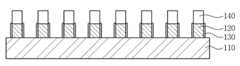
도 1a는 본 발명의 제1 실시예에 따른 편광 소자의 사시도이다.
도 1b는 도 1의 I-I'를 따른 단면도이다.
도 2는 본 발명의 제2 실시예에 따른 편광 소자의 단면도이다.
도 3은 본 발명의 제3 실시예에 따른 편광 소자의 단면도이다.
도 4는 본 발명의 제4 실시예에 따른 편광 소자의 단면도이다.
도 5는 자기조립 단분자막의 개략도이다.
도 6a 내지 6g는 도 4에 따른 편광 소자의 제조 공정도이다.
도 7은 본 발명의 제5 실시예에 따른 표시장치의 단면도이다.
도 8은 본 발명의 제6 실시예에 따른 표시장치의 단면도이다.1A is a perspective view of a polarizing device according to a first embodiment of the present invention.
FIG. 1B is a cross-sectional view taken along line II′ of FIG. 1 .
2 is a cross-sectional view of a polarizing device according to a second embodiment of the present invention.
3 is a cross-sectional view of a polarizing device according to a third embodiment of the present invention.
4 is a cross-sectional view of a polarizing device according to a fourth embodiment of the present invention.
5 is a schematic diagram of a self-assembled monolayer.
6A to 6G are flowcharts of a manufacturing process of the polarizer according to FIG. 4 .
7 is a cross-sectional view of a display device according to a fifth embodiment of the present invention.
8 is a cross-sectional view of a display device according to a sixth embodiment of the present invention.
이하, 실시예들을 중심으로 본 발명을 상세하게 설명한다. 그러나, 본 발명의 범위가 하기 설명하는 도면이나 실시예들에 의하여 한정되는 것은 아니다. 첨부된 도면들은 다양한 실시예들 중 본 발명을 구체적으로 설명하기 위하여 예시적으로 선택된 것일 뿐이다.Hereinafter, the present invention will be described in detail focusing on examples. However, the scope of the present invention is not limited by the drawings or examples described below. The accompanying drawings are only illustratively selected to specifically describe the present invention among various embodiments.
발명의 이해를 돕기 위해, 도면에서 각 구성요소와 그 형상 등이 간략하게 그려지거나 또는 과장되어 그려지기도 하며, 실제 제품에 있는 구성요소가 표현되지 않고 생략되기도 한다. 따라서 도면은 발명의 이해를 돕기 위한 것으로 해석해야 한다. 한편, 도면에서 동일한 역할을 하는 요소들은 동일한 부호로 표시된다.In order to help the understanding of the invention, each component and its shape in the drawings may be briefly drawn or drawn exaggeratedly, and the components in the actual product may be omitted without being expressed. Accordingly, the drawings should be interpreted as helping the understanding of the invention. On the other hand, elements that play the same role in the drawings are denoted by the same reference numerals.
명세서 전체에서, 어떤 부분이 다른 부분과 "연결"되어 있다고 할 때, 이는 "직접적으로 연결"되어 있는 경우뿐 아니라, 그 중간에 다른 소자를 사이에 두고 "전기적으로 연결"되어 있는 경우도 포함한다. 또한 어떤 부분이 어떤 구성요소를 "포함"한다고 할 때, 이는 특별히 반대되는 기재가 없는 한 다른 구성요소를 제외하는 것이 아니라 다른 구성요소를 더 포함할 수 있는 것을 의미한다.Throughout the specification, when a part is "connected" with another part, this includes not only the case of being "directly connected" but also the case of being "electrically connected" with another element interposed therebetween. . In addition, when a part "includes" a certain component, this means that other components may be further included rather than excluding other components unless otherwise stated.
또한, 어떤 층이나 구성요소가 다른 층이나 또는 구성요소의 "상"에 있다라고 기재되는 경우에는, 상기 어떤 층이나 구성요소가 상기 다른 층이나 구성요소와 직접 접촉하여 배치된 경우뿐만 아니라, 그 사이에 제3의 층이 개재되어 배치된 경우까지 모두 포함하는 의미이다.
Also, when a layer or component is described as being "on" another layer or component, the layer or component is placed in direct contact with the other layer or component, as well as when the layer or component is placed in direct contact with the other layer or component. It is meant to include all the cases in which the third layer is interposed therebetween.
이하, 도 1a 및 1b를 참조하여 본 발명의 제1 실시예를 설명한다.Hereinafter, a first embodiment of the present invention will be described with reference to FIGS. 1A and 1B.
도 1a는 본 발명의 제1 실시예에 따른 편광 소자(101)의 사시도이고, 도 1b는 도 1a의 I-I'를 따른 단면도이다.1A is a perspective view of a
도 1a 및 1b를 참조하면, 편광 소자(101)는 기판(110), 기판(110)상에 배치된 복수개의 금속선(120) 및 금속선(120)의 표면에 배치된 소수성 코팅층인 자기조립 단분자막(130)을 포함한다.1A and 1B, the
기판(110)은 투과성, 내열성, 내화학성 등이 우수한 물질로 만들어질 수 있다, 예를 들어, 기판(110)은 광 투과성이 우수한 유리, 폴리에틸렌나프탈레이트, 폴리에틸렌테레프탈레이트 및 폴리아크릴 중 어느 하나로 만들어질 수 있다.The
복수개의 금속선(120)이 서로 나란하게 기판(110)상에 배치된다. 각각의 금속선(120)은 한 방향으로 연장된 라인 형태를 가지며, 제1 폭(w1) 및 제1 높이(t1)를 갖는다. 또한, 인접한 금속선(120)들은 제1 간격(s1)으로 서로 이격된다.A plurality of
이러한 복수개의 금속선(120)들은 와이어 그리드(wire grid)를 구성한다. 와이어 그리드는 편광판 역할을 한다. 즉, 도 1a 및 1b에 도시된 편광 소자(101)는 와이어 그리드 편광 소자다(Wire Grid Polarizer; WGP).The plurality of
금속선(120)은 알루미늄(Al), 금(Au), 은(Ag), 구리(Cu), 크롬(Cr), 철(Fe) 및 니켈(Ni) 중 어느 하나 이상을 포함할 수 있다.The
편광 소자(101)가 우수한 편광기능을 수행하기 위해, 광이 통과하는 부분인 제1 간격(s1)이 입사광의 파장보다 짧아야 한다. 예를 들어, 입사광이 가시광선인 경우, 가시광선의 파장은 약 400 내지 700nm이므로, 제1 간격(s1)이 약 400nm 이하이면 편광 특성을 기대할 수 있다. 양호한 편광 기능을 위해, 본 발명의 제1 실시예에 따른 편광 소자(101)는 50 내지 200nm 범위의 제1 간격(s1)을 갖는다. 구체적으로 제1 간격(s1)은 100nm 이하가 될 수 있다.In order for the
또한, 금속선(120)이 배치되어 광이 통과하지 못하는 부분, 즉, 금속선(120)의 제1 폭(w1)도 50 내지 200nm 범위로 설계된다. 구체적으로 제1 폭(w1)은 100nm 이하가 될 수 있다.In addition, the portion where the
편광 효율 향상을 위해, 금속선(120)의 두께인 제1 높이(t1)는 50 내지 250nm 범위일 수 있다. 예를 들어, 제1 높이(t1)는 150nm 일 수 있다.In order to improve polarization efficiency, the first height t1 , which is the thickness of the
소수성 코팅층은 금속선(120)의 표면에 배치된다. 본 발명의 제1 실시예에서, 소수성 코팅층은 자기조립 단분자막(Self-Assembled Monolayer; SAM)(130)이다.The hydrophobic coating layer is disposed on the surface of the
자기조립 단분자막(130)은 0.2 내지 5nm의 두께를 갖는다. 자기조립 단분자막(130)의 두께가 0.2nm보다 작은 경우 막 형성이 용이하지 않을 수 있으며, 5.0nm 보다 큰 경우 자기조립 단분자막의 표면이 불균일해질 수 있다.The self-assembled
자기조립 단분자막(130)의 일단은 금속선(120)과 접촉하며, 금속선(120)과 접촉하지 않는 자기조립 단분자막(130)의 타단은 소수성기를 갖는다. 그에 따라 자기조립 단분자막(130)으로 코팅된 금속선(120)의 표면이 소수성을 갖는다.One end of the self-assembled
자기조립 단분자막(130)은 도 5를 참조하여 아래에서 보다 상세히 설명된다.
The self-assembled
이하, 도 2를 참조하여 본 발명의 제2 실시예를 설명한다. 도 2는 본 발명의 제2 실시예에 따른 편광 소자(102)의 단면도이다. 이하 중복을 피하기 위해, 이미 설명된 구성요소에 대한 상세한 설명은 생략된다.Hereinafter, a second embodiment of the present invention will be described with reference to FIG. 2 . 2 is a cross-sectional view of a
본 발명의 제2 실시예에 따른 편광 소자(102)는 기판(110), 기판(110)상에 배치된 복수개의 금속선(120), 금속선(120)상에 배치된 보호막(150) 및 금속선(120)의 표면에 배치된 소수성 코팅층인 자기조립 단분자막(130)을 포함한다.The
보호막(150)은 금속선(120) 상부에 배치되는데, 복수개의 금속선(120)에 걸쳐 하나의 판 형태로 배치된다. 보호막(150)은 절연성 재료로 만들어질 수 있는데, 예를 들어, 실리콘 질화물(SiNx)로 만들어질 수 있다. 그러나 보호막(150)의 재료가 실리콘 질화물(SiNx)로 한정되는 것은 아니며, 당업계에 알려진 공지의 다른 절연재료로 만들어질 수도 있다.The
보호막(150)은 증착에 의하여 만들어질 수 있다. 보호막(150)의 증착과정에서 보호막(150) 형성재료가 금속선(120) 표면 또는 금속선(120) 사이에 증착되는 경우 금속선(120) 사이의 간격이 일정하게 유지되지 않아 편광 소자(103)의 편광 특성이 저하될 수 있다. 반면, 제2 실시예와 같이, 금속선(120)의 표면에 소수성 코팅층이 형성되어 있는 경우 보호막(150) 형성재료가 금속선(120) 사이에 증착되는 것이 방지된다. 그에 따라, 금속선(120) 사이의 간격이 일정하게 유지되어 편광 소자(103)의 편광 특성이 유지될 수 있다.The
금속선(120) 사이의 공간은 공기로 채워질 수도 있고, 불활성 기체로 채워질 수도 있다. 또는 금속선(120) 사이의 공간(132)이 투명 고분자 수지로 채워질 수도 있다.
The space between the
이하, 도 3을 참조하여 본 발명의 제3 실시예를 설명한다. 도 3은 본 발명의 제3 실시예에 따른 편광 소자(103)의 단면도이다.Hereinafter, a third embodiment of the present invention will be described with reference to FIG. 3 . 3 is a cross-sectional view of a
본 발명의 제3 실시예에 따른 편광 소자(103)는 기판(110), 기판(110)상에 배치된 복수개의 금속선(120), 각각의 금속선(120)상에 배치된 복수개의 마스크(140) 및 금속선(120)의 표면에 배치된 소수성 코팅층인 자기조립 단분자막(130)을 포함한다.The
마스크(140)는 각각의 금속선(120) 상부에 배치되며, 금속선(120)과 마찬가지로 한 방향으로 연장된 라인 형태를 가진다. 마스크(140)는 금속선(120)의 상부를 보호한다. 마스크(140)는, 예를 들어, 실리콘 산화물(SiOx)로 만들어질 수 있다. 그러나 마스크(140) 형성 재료가 이에 한정되는 것은 아니며, 마스크(140)는 공지의 절연 재료 또는 보호막 재료로 만들어질 수도 있다.The
마스크(140)의 높이(t2)에 특별한 제안이 있는 것은 아니다. 마스크(140)는 금속층(120)과 동일한 높이를 가질 수 있다. 마스크(140)의 높이(t2)는 금속층(120)의 높이(t1)보다 클 수도 있고 작을 수도 있다.
There is no special suggestion for the height t2 of the
이하, 도 4를 참조하여 본 발명의 제4 실시예를 설명한다. 도 4는 본 발명의 제4 실시예에 따른 편광 소자(104)의 단면도이다.Hereinafter, a fourth embodiment of the present invention will be described with reference to FIG. 4 . 4 is a cross-sectional view of a
본 발명의 제4 실시예에 따른 편광 소자(104)는 기판(110), 기판(110)상에 배치된 복수개의 금속선(120), 각각의 금속선(120)상에 배치된 복수개의 마스크(140), 마스크(140)상에 배치된 보호막(150) 및 금속선(120)의 표면에 배치된 소수성 코팅층인 자기조립 단분자막(130)을 포함한다.The
보호막(150)은 마스크(140)상에 배치되는데, 복수개의 마스크(140)에 걸쳐 하나의 판 형태로 배치된다. 보호막(150)은 절연성 재료로 만들어질 수 있는데, 예를 들어, 실리콘 질화물(SiNx)로 만들어질 수 있다. 보호막(150)은 증착에 의하여 만들어질 수 있다. 금속선(120)의 표면에 자기조립 단분자막(130)으로 된 소수성 코팅층이 형성되어 있기 때문에, 증착 과정에서 보호막(150) 형성재료가 금속선(120) 사이에 증착되는 것이 방지된다. 금속선(120) 사이의 공간(132)은 공기, 불활성 기체 또는 투명 고분자 수지로 채워질 수 있다.
The
이하 도 5를 참조하여 자기조립 단분자막(130)을 설명한다. 도 5는 자기조립 단분자막(130)의 일례에 대한 구조도이다.Hereinafter, the self-assembled
자기조립 단분자막(130)은 화학식 1로 표현되는 화합물을 포함할 수 있다.The self-assembled
[화학식 1][Formula 1]

여기서, Y는 치환기와 결합되거나 결합되지 않은 황(S), 규소(Si), 인(P) 및 탄소(C) 중 어느 하나일 수 있다.Here, Y may be any one of sulfur (S), silicon (Si), phosphorus (P), and carbon (C), which may or may not be bonded to a substituent.
Y와 결합된 산소(O)는 금속선(120)의 금속원자와 결합된다.Oxygen (O) combined with Y is combined with a metal atom of the
R은 치환되거나 치환되지 않은 탄소수 2 내지 50의 탄화수소계 화합물일 수 있다. 예를 들어, R은 치환 또는 비치환된 C6-C30의 방향족기, 하나 이상의 헤테로 원자를 포함하는 치환 또는 비치환된 C5-C30의 헤테로방향족기, 치환 또는 비치환된 C1-C20의 알킬기 및 주쇄에


X는 소수성 작용기(hydrophobic group)이다. X의 예로 CFn, CBrm, 치환 또는 비치환 아릴기 등이 있다. 여기서 n과 m는 1 내지 3의 정수이다. 이러한 소수성 작용기(X)로 인하여, 자기조립 단분자막(130)은 소수성을 가지며 소수성 코팅층을 형성한다.X is a hydrophobic group. Examples of X include CFn , CBrm , and a substituted or unsubstituted aryl group. Here, n and m are integers from 1 to 3. Due to the hydrophobic functional group (X), the self-assembled
화학식 1로 표현되는 화합물의 예로 화학식 2로 표현되는 화합물이 있다.Examples of the compound represented by the formula (1) include a compound represented by the formula (2).
[화학식 2][Formula 2]

여기서 n은 1 내지 30의 정수이다.Here, n is an integer from 1 to 30.
자기조립 단분자막(130) 형성에 사용되는 화합물로, 예를 들어, 퍼플루오르데실포스포닉산(Perfluorodecylphosphonic acid; PFDP), 퍼플루오르데실디메틸클로로실란(Perfluorodecyldimethychlorosilane; PFMS) 등이 있으며, 말단이 소수성기로 치환된 옥타데실포스포닉산(Octadecylphosphonic acid; ODP), 데실포스포닉산(Decylphosphonic acid; DP), 옥틸포스포닉산(Octylphosphonic acid; OP) 등이 있다.As a compound used to form the self-assembled
자기조립 단분자막(130) 형성용 화합물의 다른 예로, 말단의 산기가 소수성기로 치환된 11-머캅토운데카노익산(11-mercaptoundecanoic acid, MUA), 11-하이드록시-1-운데칸티올(11-hydroxy-1-undecanethiol), 12-머캅토오데카노익산(12- mercaptododecanoic acid, 19-하이드록시-1-헥사데칸티올 (16-hydroxy-1- hexadecanethiol), 16-머캅토헥사데카노익산(16-mercaptohexadecanoic acid), 카르복시헥사데실 디설파이드(Carboxyhexadecyl disulfide), 하이드록시헥사데실 디설파이드(Hydroxyhexadecyl disulfide), 하이드록시운데실 디설파이드(Hydroxyundecyl disulfide). 테트라(에틸글리콜)운데실 디설파이드[Tetra(ethylene glycol) undecyl disulfide] 등이 있다.As another example of the compound for forming the self-assembled
예를 들어, 자기조립 단분자막(130)은 디클로로포스포릴기를 함유하는 하기 화학식 3으로 표시되는 화합물로 만들어질 수 있다.For example, the self-assembled
[화학식 3][Formula 3]

화학식 3에서 R과 X는 화학식 1에서 정의된 것과 동일하다.In Formula 3, R and X are the same as defined in Formula 1.
화학식 3으로 표시되는 화합물은 하기 화학식 4 내지 6으로 표현되는 화합물 중 어느 하나일 수 있다.The compound represented by Formula 3 may be any one of compounds represented by Formulas 4 to 6 below.
[화학식 4][Formula 4]

화학식 4에서, Z는 황, 질소, 탄소 및 산소 중 어느 하나이고, m은 0 내지 20의 정수이고, n은 0 내지 20의 정수이다.In Formula 4, Z is any one of sulfur, nitrogen, carbon, and oxygen, m is an integer from 0 to 20, and n is an integer from 0 to 20.
[화학식 5][Formula 5]

화학식 5에서, X1, X2, X3, X4, X5는 각각 독립적으로 수소; 할로겐; 또는 수소, 할로겐, 산소 또는 질소 중 하나 이상으로 치환된 C1-C30의 알킬기;이고, m은 1 내지 20의 정수이고, n은 0 내지 20의 정수이다.In Formula 5, X1, X2, X3, X4, and X5 are each independently hydrogen; halogen; or a C1-C30 alkyl group substituted with one or more of hydrogen, halogen, oxygen, or nitrogen; m is an integer from 1 to 20, and n is an integer from 0 to 20.
[화학식 6][Formula 6]

화학식 6에서, X6는 각각 독립적으로 할로겐 또는 CF3이고, h는 1 내지 5의 정수이다.In Formula 6, each X6 is independently halogen or CF3 , and h is an integer of 1 to 5.
또한, 화학식 3으로 표시되는 화합물은 하기 화학식 7 내지 17로 표현되는 화합물 중 어느 하나일 수 있다.In addition, the compound represented by Formula 3 may be any one of compounds represented by Formulas 7 to 17 below.
[화학식 7][Formula 7]

[화학식 8][Formula 8]

[화학식 9][Formula 9]

[화학식 10][Formula 10]

[화학식 11][Formula 11]

[화학식 12][Formula 12]

[화학식 13][Formula 13]

[화학식 14][Formula 14]

[화학식 15][Formula 15]

[화학식 16][Formula 16]

[화학식 17][Formula 17]

이하, 도 6a 내지 6g를 참조하여 본 발명의 제4 실시예에 따른 편광 소자(104)의 제조방법을 설명한다. 도 6a 내지 6g는 도 4에 따른 편광 소자의 제조 공정도이다.Hereinafter, a method of manufacturing the
도 6a를 참조하면, 기판(110)상에 금속층(121)이 형성된다. 기판(110)은 투과성, 내열성, 내화학성 등이 우수한 물질로 만들어질 수 있다. 예를 들어, 기판(110)은 광 투과성이 우수한 유리, 폴리에틸렌나프탈레이트, 폴리에틸렌테레프탈레이트층 및 폴리아크릴 중 어느 하나로 만들어질 수 있다.Referring to FIG. 6A , a
금속층(121)은 알루미늄(Al), 금(Au), 은(Ag), 구리(Cu), 크롬(Cr), 철(Fe) 및 니켈(Ni) 중 어느 하나 이상을 포함할 수 있다. 금속층(121)은 증착에 의하여 형성될 수 있다. 금속층(121)은 100nm 내지 200nm의 두께를 가질 수 있다. 예를 들어 금속층(121)은 약 150nm의 두께를 가질 수 있다.The
금속층(121)의 두께는 제1 폭(도 1b의 w1)을 고려하여 결정될 수 있다. 편광에 필요한 금속선(120)의 간격과 금속선(120)의 강도를 고려하여, 금속층(121)의 두께는 제1 폭(w1) 또는 제1 간격(s1)의 약 3배 정도가 될 수 있다.The thickness of the
금속층(121) 상에 마스크층(141)이 형성된다. 마스크층(141)은, 예를 들어 실리콘 산화물(SiOx)를 포함할 수 있다. 이러한 실리콘 산화물(SiOx)로 이산화 규소(SiO2)가 있다. 마스크층(141)는 화학 기상 증착(chemical vapor deposition)에 의해 형성될 수 있다. 마스크층(141)에 의해 금속층(121)의 표면이 보호된다.A
마스크층(141)은 금속층(121)과 동일한 두께를 가질 수 있다. 또한, 마스크층(141)은 금속층보다 두꺼울 수도 있고 얇을 수도 있다. 예를 들어, 마스크층(141)은 약 150nm의 두께를 가질 수 있다.The
도 6b를 참조하면, 마스크층(141) 상에 레지스트층(311)이 배치된다. 레지스트층(150)은 당해 기술 분야에서 사용되는 공지의 레지스트 물질로 만들어질 수 있다. 레지스트층(311)은 유기물로 만들어질 수 있다.Referring to FIG. 6B , a resist
도 6c를 참조하면, 레지스트층(311)이 패턴화되어 복수개의 레지스트 패턴(310)이 형성된다. 레지스트 패턴(310)은 패턴 마스크를 이용한 광조사 및 현상에 의하여 만들어질 수 있고, 몰드를 이용한 임프린트(imprint) 방법에 의하여 만들어질 수도 있다.Referring to FIG. 6C , the resist
레지스트 패턴(310)의 단면은 제1 폭(w1)을 갖는 돌출부 형태이며, 복수의 레지스트 패턴(310)이 제1 간격(s1)으로 서로 이격된다. 여기서, 제1 폭(w1)과 제1 간격(s1)의 비는 약 1:1 일 수 있다. 구체적으로 제1 폭(w1)은 약 30nm 내지 60nm 이고, 제1 간격(s1)은 약 30nm 내지 60nm일 수 있는데, 예를 들어, 제1 폭(w1)은 약 50nm 이고, 제1 간격(s1)은 약 50nm 일 수 있다.A cross-section of the resist
도 6d를 참조하면, 마스크층(141)과 금속층(121)이 식각되어, 금속선(120)과 마스크(140)가 형성된다. 각각의 금속선(120)은 제1 폭(w1)을 가지며, 복수개의 금속선(120)이 제1 간격(s1)으로 서로 이격된다.Referring to FIG. 6D , the
도 6e를 참조하면, 레지스트 패턴(310)이 제거되어, 금속선(120) 및 금속선(120)상에 배치된 마스크(140)를 포함하는 와이어 그리드(wire grid) 패턴이 형성된다. 와이어 그리드 패턴의 규격은 금속선(120)과 마스크(140)의 높이(t1, t2), 제1 폭(w1) 및 제1 간격(s1)에 따라 결정된다.Referring to FIG. 6E , the resist
도 6f를 참조하면, 금속선(120)의 표면에 자기조립 단분자막(130)이 형성된다. 자기조립 단분자막(130)은 말단이 소수성을 갖는 코팅층이다.Referring to FIG. 6F , the self-assembled
자기조립 단분자막(130)을 형성하는 방법으로 액상 공정(solution process)과 기상 공정(vapor process)이 있다.As a method of forming the self-assembled
액상 공정으로 침지법(dipping), 미세접촉인쇄법(micro-contact printing), 스핀코팅법(spin-coating) 등이 있다. 액상공정에는 용매가 사용된다.The liquid phase process includes dipping, micro-contact printing, and spin-coating. A solvent is used in the liquid phase process.
침지법은 와이어 그리드 패턴(120, 140)이 배치된 기판(110)을 유기용매와 자기조립 단분자막 형성 물질이 혼합된 혼합물에 일정 시간 침지하여 자기조립 단분자막(130)을 형성하는 방법이다. 스핀코팅법은 유기용매와 자기조립 단분자막 형성 물질이 혼합된 혼합용액을 스포이트 등을 이용하여 기판(110)위에 떨어뜨리고, 기판(110)을 회전시켜 혼합액을 고르게 분포시킨 후 가열하여 자기조립 단분자막(130)을 형성하는 방법이다. 미세접촉인쇄법은 탄성중합체(elastomer)로 만들어진 도장에 자기조립 단분자막 형성 재료를 묻힌 후 이를 금속선(120)과 접촉시켜 자기조립 단분자막(110)을 형성하는 방법이다.The immersion method is a method of forming the self-assembled
기상 공정의 예로 증착 방법이 있다.An example of a vapor phase process is a deposition method.
도 6g를 참조하면, 마스크(140)상에 보호막(150)이 형성된다.Referring to FIG. 6G , a
보호막(150)은 복수개의 마스크(140)에 걸쳐 하나의 판 형태로 형성된다. 보호막(150)은 절연성 재료로 만들어질 수 있는데, 예를 들어, 실리콘 질화물(SiNx)로 만들어질 수 있다.The
보호막(150)은 증착에 의하여 만들어질 수 있다. 금속선(120)의 표면에 소수성 코팅층인 자기조립 단분자막(130)이 형성되어 있기 때문에 증착과정에서 보호막(150) 형성재료가 금속선(120) 또는 금속선(120) 사이에 증착되는 것이 방지된다.
The
이하, 도 7을 참조하여 본 발명에 제5 실시예에 따른 표시장치를 설명한다.Hereinafter, a display device according to a fifth embodiment of the present invention will be described with reference to FIG. 7 .
도 7은 본 발명의 제5 실시예에 따른 표시장치(105)의 단면도이다.7 is a cross-sectional view of a
표시장치(105)은 어레이 기판(201), 대향 기판(202) 및 어레이 기판(201)과 대향 기판(202) 사이에 배치되는 액정층(183)을 포함한다.The
어레이 기판(201)은 제1 기판(111), 금속선(120), 마크스(140), 보호막(150), 게이트 절연막(170), 박막트랜지스터(177), 평탄화막(160) 및 제1 전극(181)을 포함한다.The
금속선(120)은 제1 기판(111)상에 배치된다. 금속선(120) 상부에 마스크(140)가 배치되고, 금속선(120)의 표면에 자기조립 단분자막(130)이 배치된다. 제1 기판(111)상에 배치된 금속선(120)과 마스크(140)는 하부 와이어 그리드 패턴을 형성한다. 금속선(120)은 제1 기판(111)의 전면에 배치될 수도 있고, 일부에 배치될 수도 있다. 제5 실시예에서 금속선(120)은 제1 기판(111)의 전면에 배치된다. 금속선(120), 마스크(140) 및 자기조립 단분자막(130)은 이미 설명되었으므로, 이들에 대한 자세한 설명은 생략된다.The
마스크(140)상에 보호막(150)이 배치된다. 보호막(150)은 실리콘 산화물(SiOx) 또는 실리콘 질화물(SiNx)을 포함할 수 있다.A
보호막(150) 상에 게이트 전극(171) 및 게이트 라인(미도시)이 배치된다. 게이트 라인은 금속선(120)과 수직 방향, 수평 방향 또는 소정의 각도를 갖는 사선 방향으로 배치될 수 있다.A
게이트 전극(171) 및 게이트 라인이 배치된 보호막(150)상에 게이트 절연막(170)이 배치된다. 게이트 절연막(170)은 실리콘 질화물(SiNx) 또는 실리콘 산화물(SiOx)등의 무기 물질로 만들어질 수 있다.A
게이트 절연막(170) 상에 반도체층(173)이 배치된다. 반도체층(173)은 실리콘을 포함할 수 있고, 산화물 반도체를 포함할 수도 있다. 산화물 반도체는, 예를 들어, 인듐(indium: In), 아연(zinc: Zn), 갈륨(gallium: Ga), 주석(tin: Sn) 및 하프늄(hafnium: Hf) 중 적어도 하나를 포함할 수 있다.A
반도체층(173)상에 반도체층(173)과 적어도 일부가 중첩된 소스 전극(175) 및 드레인 전극(176)이 배치된다. 소스 전극(175)과 드레인 전극(176)은 서로 이격되어 있는데, 소스 전극(175)은 데이터 라인(미도시)와 연결되고, 드레인 전극(176)은 제1 전극(181)과 연결된다.A
게이트 전극(171), 소스 전극(175), 드레인 전극(176) 및 반도체층(176)은 박막트랜지스터(177)를 구성한다.The
박막트랜지스터(177) 상에 평탄화막(160)이 배치된다. 평탄화막(160)은 실리콘 질화물(SiNx), 실리콘 산화물(SiOx) 등의 무기 물질로 만들어질 수도 있고, 유기 물질로 만들어질 수도 있다. 또한 평탄화막(160)은 무기막과 유기막을 포함하는 다중막 구조를 가질 수도 있다. 평탄화막(160)은 드레인 전극(176)의 일부를 노출하는 콘택홀(161)을 갖는다.A
평탄화막(160)상에 제1 전극(181)이 배치된다. 제1 전극(181)은 화소 영역에 대응되어 배치되며, 콘택홀(161)을 통하여 드레인 전극(176)과 연결된다.A
대향 기판(202)은 제2 기판(211), 금속선(220), 마스크(240), 보호막(250), 컬러필터(191), 블랙 매트릭스(192), 오버 코팅층(193) 및 제2 전극(182)을 포함한다.The
제1 기판(111)과 대향되는 제2 기판(211)의 일면에 금속선(220)이 배치되고, 금속선(220)상에 마스크(240)가 배치된다. 금속선(220)의 표면에 자기조립 단분자막(230)이 배치된다. 제2 기판(211)상에 배치된 금속선(220)과 마스크(240)는 상부 와이어 그리드 패턴을 형성한다. 금속선(220)은 제2 기판(211)의 전면에 배치될 수도 있고, 일부에 배치될 수도 있다. 제4 실시예에서 금속선(220)은 제2 기판(211)의 전면에 배치된다. 금속선(220), 마스크(240) 및 자기조립 단분자막(230)은 이미 설명되었으므로 자세한 설명은 생략된다.A
마스크(240)상에 보호막(250)이 배치된다. 보호막(250)은 실리콘 산화물(SiOx) 또는 실리콘 질화물(SiOx)을 포함할 수 있다.A
보호막(250)상에 블랙 매트릭스(BM)가 배치된다. 블랙 매트릭스(192)는 화소 영역 이외의 영역에 대응되어 배치되어 화소 영역을 정의한다. 예를 들어, 블랙 매트릭스(192)는 데이터 라인, 게이트 라인 및 박막트랜지스터(177)와 중첩할 수 있다.A black matrix BM is disposed on the
컬러 필터(191)는 블랙 매트릭스(192)에 의해 정의되는 화소 영역에 배치된다. 컬러 필터(191)는 액정층(183)을 투과하는 광에 색을 제공한다. 컬러 필터(191)는 적색 컬러 필터(red), 녹색 컬러 필터(green) 및 청색 컬러 필터(blue) 중 어느 하나일 수 있다. 제5 실시예에서 컬러 필터(191)는 블랙 매트릭스(192)와 일부 중첩한다.The
컬러 필터(191)와 블랙 매트릭스(192)상에 오버 코팅층(193)이 배치된다. 오버 코팅층(193)은 컬러 필터(191) 상부를 평탄화하면서, 컬러 필터(191)를 보호한다. 오버 코팅층(193)은, 예를 들어, 아크릴계 에폭시 재료로 만들어질 수 있다.An
오버 코팅층(193)상에 제2 전극(182)이 배치된다. 제2 전극(182)은 공통 라인(미도시)과 전기적으로 연결된다. 제2 전극(182)은 복수의 개구를 갖는 슬릿 패턴을 가질 수도 있다. 제2 전극(182)은 투명 도전 물질을 포함할 수 있다. 예를 들어, 제2 전극(182)은 산화 인듐 주석(indium tin oxide: ITO) 또는 산화 아연 주석(indium zinc oxide: IZO)으로 만들어질 수 있다.A
액정층(183)은 어레이 기판(201)과 대향 기판(202) 사이에 배치된다. 액정층(183)은 광학적 이방성을 갖는 액정 분자들을 포함한다. 액정 분자들은 전계에 의해 정렬이 변경되어 액정층(183)을 지나는 광의 투과량을 조정한다.
The
이하, 도 8을 참조하여 본 발명에 제6 실시예에 따른 표시장치를 설명한다.Hereinafter, a display device according to a sixth embodiment of the present invention will be described with reference to FIG. 8 .
도 8은 본 발명의 제6 실시예에 따른 표시장치(106)의 단면도이다.8 is a cross-sectional view of the
도 8을 참조하면, 제6 실시예에 따른 표시장치(106)는 제1 기판(111)과 제2 기판(211)에 배치된 금속선(120, 220), 마스크(140, 240) 및 보호막(150, 250)의 위치를 제외하고, 도 7의 표시장치(105)와 실질적으로 동일하다. 따라서 중복되는 부분에 대한 설명은 생략된다.Referring to FIG. 8 , the
구체적으로, 제1 기판(111)의 일면에 게이트 절연막(170), 박막트랜지스터(177), 평탄화막(160) 및 제1 전극(181)이 배치되고, 제1 기판(111)의 타면에 금속선(120)과 마스크(140)가 배치되어 하부 와이어 그리드 패턴이 형성된다. 또한, 금속(120)선의 표면에 자기조립 단분자막(130)이 배치되고, 마스크(140)상에 보호막(150)이 배치되어 금속선(120)을 보호한다. 여기서, 제1 기판(111)의 일면은 제2 기판(211)을 향하는 면이고, 제1 기판(111)의 타면은 제2 기판(211)과 대향되는 면의 반대면이다.Specifically, a
제2 기판(211)의 일면에 컬러필터(191), 블랙 매트릭스(192), 오버코팅층(193) 및 제2 전극(182)이 배치되고, 제2 기판(211)의 타면에 금속선(220)과 마스크(240)가 배치되어 상부 와이어 그리드 패턴이 형성된다. 또한, 금속(220)선의 표면에 자기조립 단분자막(230)이 배치되고, 마스크(240)상에 보호막(250)이 배치되어 금속선(220)을 보호한다. 여기서, 제2 기판(211)의 일면은 제1 기판(111)을 향하는 면이고, 제2 기판(211)의 타면은 제1 기판(111)과 대향되는 면의 반대면이다.
A
이상에서, 도면에 도시된 예들을 참고하여 본 발명을 설명하였으나, 이러한 설명은 예시적인 것에 불과하며, 당해 기술 분야에서 통상의 지식을 가진 자라면 이로부터 다양한 변형 및 균등한 다른 실시예가 가능할 것이다. 따라서, 본 발명의 기술적 보호 범위는 첨부된 특허청구범위의 기술적 사상에 의하여 정해져야 할 것이다.In the above, the present invention has been described with reference to the examples shown in the drawings, but these descriptions are merely exemplary, and various modifications and equivalent other embodiments will be possible therefrom by those skilled in the art. Accordingly, the technical protection scope of the present invention should be defined by the technical spirit of the appended claims.
110: 기판111: 제1 기판
120: 금속선130: 자기조립 단분자막
140: 마스크150: 보호막
160: 평탄화막161: 콘택홀
170: 게이트 절연막181: 제1 전극
182: 제2 전극183: 액정층
191: 컬러 필터192: 블랙 매트릭스
210: 대향 기판211: 제2 기판
w1: 제1 폭s1: 제1 간격
t1: 제1 두께t2: 제2 두께110: substrate 111: first substrate
120: metal wire 130: self-assembled monolayer
140: mask 150: shield
160: planarization film 161: contact hole
170: gate insulating layer 181: first electrode
182: second electrode 183: liquid crystal layer
191: color filter 192: black matrix
210: counter substrate 211: second substrate
w1: first width s1: first interval
t1: first thickness t2: second thickness
Claims (19)
Translated fromKorean상기 기판상에 배치되고, 각각 제1 폭 및 제1 높이를 갖고, 제1 간격으로 서로 이격되어 나란히 배치된 복수개의 금속선; 및
상기 금속선의 표면에 배치된 소수성 코팅층;
을 포함하고,
상기 소수성 코팅층은 하기 화학식 1로 표현되는 화합물을 포함하는 자기조립 단분자막(Self-Assembled Monolayer)인, 편광 소자:
[화학식 1]

여기서, Y는 치환기와 결합되거나 결합되지 않은 황(S), 규소(Si), 인(P) 및 탄소(C) 중 어느 하나이며,
R은 치환 또는 비치환된 C6-C30의 방향족기, 하나 이상의 헤테로 원자를 포함하는 치환 또는 비치환된 C5-C30의 헤테로방향족기, 치환 또는 비치환된 C1-C20의 알킬기 및 주쇄에


X는 CFn, CBrm, 치환 또는 비치환 아릴기이다.Board;
a plurality of metal wires disposed on the substrate, each having a first width and a first height, and spaced apart from each other at a first interval and arranged side by side; and
a hydrophobic coating layer disposed on the surface of the metal wire;
including,
The hydrophobic coating layer is a self-assembled monolayer (Self-Assembled Monolayer) including a compound represented by the following formula (1), a polarizing device:
[Formula 1]
Here, Y is any one of sulfur (S), silicon (Si), phosphorus (P), and carbon (C) bonded to or not bonded to a substituent,
R is a substituted or unsubstituted C6-C30 aromatic group, a substituted or unsubstituted C5-C30 heteroaromatic group containing one or more hetero atoms, a substituted or unsubstituted C1-C20 alkyl group, and in the main chain
X is CFn , CBrm , a substituted or unsubstituted aryl group.
[화학식 3]

여기서, R은 치환 또는 비치환된 C6-C30의 방향족기, 하나 이상의 헤테로원자를 포함하는 치환 또는 비치환된 C5-C30의 헤테로방향족기, 치환 또는 비치환된 C1-C20의 알킬기 및 주쇄에


[Formula 3]
Here, R is a substituted or unsubstituted C6-C30 aromatic group, a substituted or unsubstituted C5-C30 heteroaromatic group containing one or more heteroatoms, a substituted or unsubstituted C1-C20 alkyl group and in the main chain
[화학식 4]

여기서, Z는 황, 질소, 탄소 및 산소 중 어느 하나이고, m은 0 내지 20의 정수이고, n은 0 내지 20의 정수이다:
[화학식 5]

여기서, X1, X2, X3, X4, X5는 각각 독립적으로 수소; 할로겐; 또는 수소, 할로겐, 산소 또는 질소 중 하나 이상으로 치환된 C1-C30의 알킬기;이고, m은 1 내지 20의 정수이고, n은 0 내지 20의 정수이다:
[화학식 6]

여기서, X6는 각각 독립적으로 할로겐 또는 CF3이고, h는 1 내지 5의 정수이다.The polarizing device according to claim 8, wherein the compound represented by Formula 3 is represented by any one of Formulas 4 to 6 below:
[Formula 4]
where Z is any one of sulfur, nitrogen, carbon and oxygen, m is an integer from 0 to 20, and n is an integer from 0 to 20:
[Formula 5]
Here, X1, X2, X3, X4, X5 are each independently hydrogen; halogen; or a C1-C30 alkyl group substituted with one or more of hydrogen, halogen, oxygen or nitrogen; m is an integer from 1 to 20, and n is an integer from 0 to 20:
[Formula 6]
Here, X6 is each independently halogen or CF3 , and h is an integer of 1 to 5.
상기 제1 기판상에 배치되고, 각각 제1 폭 및 제1 높이를 갖고, 제1 간격으로 서로 이격되어 나란히 배치된 복수개의 금속선;
상기 금속선의 표면에 배치된 소수성 코팅층;
제2 기판; 및
상기 제1 기판과 상기 제2 기판 사이에 배치된 액정층;
을 포함하고,
상기 소수성 코팅층은 하기 화학식 1로 표현되는 화합물을 포함하는 자기조립 단분자막(Self-Assembled Monolayer)인, 표시장치:
[화학식 1]
[화학식 1]

여기서, Y는 치환기와 결합되거나 결합되지 않은 황(S), 규소(Si), 인(P) 및 탄소(C) 중 어느 하나이며,
R은 치환 또는 비치환된 C6-C30의 방향족기, 하나 이상의 헤테로 원자를 포함하는 치환 또는 비치환된 C5-C30의 헤테로방향족기, 치환 또는 비치환된 C1-C20의 알킬기 및 주쇄에


X는 CFn, CBrm, 치환 또는 비치환 아릴기이다.a first substrate;
a plurality of metal wires disposed on the first substrate, each having a first width and a first height, and spaced apart from each other at a first interval and arranged side by side;
a hydrophobic coating layer disposed on the surface of the metal wire;
a second substrate; and
a liquid crystal layer disposed between the first substrate and the second substrate;
including,
The hydrophobic coating layer is a self-assembled monolayer including a compound represented by the following formula (1), a display device:
[Formula 1]
[Formula 1]
Here, Y is any one of sulfur (S), silicon (Si), phosphorus (P), and carbon (C) bonded to or not bonded to a substituent,
R is a substituted or unsubstituted C6-C30 aromatic group, a substituted or unsubstituted C5-C30 heteroaromatic group containing one or more hetero atoms, a substituted or unsubstituted C1-C20 alkyl group, and in the main chain
X is CFn , CBrm , a substituted or unsubstituted aryl group.
상기 제2 기판상에 배치되고, 각각 제1 폭 및 제1 높이를 갖고, 제1 간격으로 서로 이격되어 나란히 배치된 복수개의 금속선 및 상기 금속선의 표면에 배치된 소수성 코팅층을 더 포함하는 표시장치.14. The method of claim 13,
A display device further comprising: a plurality of metal wires disposed on the second substrate, each having a first width and a first height, spaced apart from each other at a first interval and disposed side by side, and a hydrophobic coating layer disposed on a surface of the metal wire.
Priority Applications (2)
| Application Number | Priority Date | Filing Date | Title |
|---|---|---|---|
| KR1020150006337AKR102332948B1 (en) | 2015-01-13 | 2015-01-13 | Polarizer device and display device comprising the same |
| US14/887,916US9933655B2 (en) | 2015-01-13 | 2015-10-20 | Polarizer and display device comprising the same |
Applications Claiming Priority (1)
| Application Number | Priority Date | Filing Date | Title |
|---|---|---|---|
| KR1020150006337AKR102332948B1 (en) | 2015-01-13 | 2015-01-13 | Polarizer device and display device comprising the same |
Publications (2)
| Publication Number | Publication Date |
|---|---|
| KR20160087477A KR20160087477A (en) | 2016-07-22 |
| KR102332948B1true KR102332948B1 (en) | 2021-12-01 |
Family
ID=56367469
Family Applications (1)
| Application Number | Title | Priority Date | Filing Date |
|---|---|---|---|
| KR1020150006337AActiveKR102332948B1 (en) | 2015-01-13 | 2015-01-13 | Polarizer device and display device comprising the same |
Country Status (2)
| Country | Link |
|---|---|
| US (1) | US9933655B2 (en) |
| KR (1) | KR102332948B1 (en) |
Families Citing this family (5)
| Publication number | Priority date | Publication date | Assignee | Title |
|---|---|---|---|---|
| CN105549236B (en)* | 2016-02-19 | 2020-05-12 | 京东方科技集团股份有限公司 | Switchable peep-proof device, preparation method thereof and display device |
| KR102581143B1 (en)* | 2016-08-18 | 2023-09-21 | 삼성디스플레이 주식회사 | Display device |
| EP3545345B1 (en)* | 2016-11-22 | 2022-11-02 | Moxtek, Inc. | Wire grid polarizer heat sink |
| WO2021114176A1 (en)* | 2019-12-12 | 2021-06-17 | 京东方科技集团股份有限公司 | Display panel and manufacturing method therefor, and display device |
| CN113874768B (en)* | 2021-07-16 | 2024-09-17 | 福建晶安光电有限公司 | Polarization element, light emitting diode and light emitting device |
Family Cites Families (6)
| Publication number | Priority date | Publication date | Assignee | Title |
|---|---|---|---|---|
| US7570424B2 (en) | 2004-12-06 | 2009-08-04 | Moxtek, Inc. | Multilayer wire-grid polarizer |
| US20090153961A1 (en) | 2005-07-22 | 2009-06-18 | Zeon Corporation | Grid Polarizer and Method for Manufacturing the Same |
| KR101211216B1 (en)* | 2005-09-28 | 2012-12-11 | 엘지디스플레이 주식회사 | method for fabricating of metal wiring, flat display device fabricated using the same and method for fabricating of flat display device using the same |
| KR101325665B1 (en)* | 2006-12-21 | 2013-11-05 | 엘지디스플레이 주식회사 | Array substrate and method for fabricating the same |
| KR101197776B1 (en)* | 2010-12-27 | 2012-11-06 | 엘지이노텍 주식회사 | method for manufacturing wire grid polarizer |
| KR101977061B1 (en) | 2012-07-10 | 2019-05-13 | 삼성디스플레이 주식회사 | Polarizer, display panel having the same and method of manufacturing the same |
- 2015
- 2015-01-13KRKR1020150006337Apatent/KR102332948B1/enactiveActive
- 2015-10-20USUS14/887,916patent/US9933655B2/enactiveActive
Also Published As
| Publication number | Publication date |
|---|---|
| US9933655B2 (en) | 2018-04-03 |
| KR20160087477A (en) | 2016-07-22 |
| US20160202552A1 (en) | 2016-07-14 |
Similar Documents
| Publication | Publication Date | Title |
|---|---|---|
| KR102332948B1 (en) | Polarizer device and display device comprising the same | |
| US9977280B2 (en) | COT type liquid crystal display device | |
| US20120038867A1 (en) | Display substrate, display device including the same, and method of manufacturing the display substrate | |
| US20130148072A1 (en) | Narrow bezel-type liquid crystal display device | |
| US9575356B2 (en) | Polarizer, display substrate, display panel having the same and method of manufacturing the same | |
| CN104011632B (en) | Touch panel and display device with touch panel | |
| KR20090100186A (en) | How to Form Metal Wiring | |
| KR101686098B1 (en) | Organic light emitting diode display device and method for fabricating the same | |
| CN103149763B (en) | TFT-LCD array substrate, display panel and preparation method thereof | |
| US20140285760A1 (en) | Liquid crystal display and method of manufacturing the same | |
| US20160322387A1 (en) | Display device and manufacturing method thereof | |
| US20130134426A1 (en) | Composition of organic insulating layer and thin film transistor substrate and display device using the same | |
| KR101960827B1 (en) | Liquid crystal composition, liquid crystal display and method of manufacturing liquid crystal display | |
| KR20160125598A (en) | Thin film transistor array substrate and method of manufacturing thereof and display device having the thin film transistor array substrate | |
| KR20070015314A (en) | LCD and its manufacturing method | |
| KR102112650B1 (en) | Flexible liquid crystal display device and method of fabricating the same | |
| KR102250491B1 (en) | A display panel and method of manufacturing a polarizer | |
| CN107526220A (en) | Display device and its manufacture method | |
| US9915844B2 (en) | Liquid crystal display and method of manufacturing the same | |
| KR102438632B1 (en) | Display device and manufacturing method of display device | |
| KR102315207B1 (en) | Display device and manufacturing method thereof | |
| US10353240B2 (en) | Display apparatus and method of manufacturing the same | |
| CN114792768A (en) | Display device | |
| WO2016045255A1 (en) | Organic thin film transistor, and preparation method, array substrate, and display device thereof | |
| CN108020965B (en) | Liquid crystal display device |
Legal Events
| Date | Code | Title | Description |
|---|---|---|---|
| PA0109 | Patent application | Patent event code:PA01091R01D Comment text:Patent Application Patent event date:20150113 | |
| PG1501 | Laying open of application | ||
| A201 | Request for examination | ||
| PA0201 | Request for examination | Patent event code:PA02012R01D Patent event date:20191226 Comment text:Request for Examination of Application Patent event code:PA02011R01I Patent event date:20150113 Comment text:Patent Application | |
| E902 | Notification of reason for refusal | ||
| PE0902 | Notice of grounds for rejection | Comment text:Notification of reason for refusal Patent event date:20210209 Patent event code:PE09021S01D | |
| E701 | Decision to grant or registration of patent right | ||
| PE0701 | Decision of registration | Patent event code:PE07011S01D Comment text:Decision to Grant Registration Patent event date:20210826 | |
| PR0701 | Registration of establishment | Comment text:Registration of Establishment Patent event date:20211125 Patent event code:PR07011E01D | |
| PR1002 | Payment of registration fee | Payment date:20211126 End annual number:3 Start annual number:1 | |
| PG1601 | Publication of registration | ||
| PR1001 | Payment of annual fee | Payment date:20241022 Start annual number:4 End annual number:4 |