KR102329497B1 - Display device and electronic device including the same - Google Patents
Display device and electronic device including the sameDownload PDFInfo
- Publication number
- KR102329497B1 KR102329497B1KR1020217012853AKR20217012853AKR102329497B1KR 102329497 B1KR102329497 B1KR 102329497B1KR 1020217012853 AKR1020217012853 AKR 1020217012853AKR 20217012853 AKR20217012853 AKR 20217012853AKR 102329497 B1KR102329497 B1KR 102329497B1
- Authority
- KR
- South Korea
- Prior art keywords
- transistor
- electrode
- oxide semiconductor
- layer
- gate
- Prior art date
- Legal status (The legal status is an assumption and is not a legal conclusion. Google has not performed a legal analysis and makes no representation as to the accuracy of the status listed.)
- Active
Links
Images


Classifications
- G—PHYSICS
- G09—EDUCATION; CRYPTOGRAPHY; DISPLAY; ADVERTISING; SEALS
- G09G—ARRANGEMENTS OR CIRCUITS FOR CONTROL OF INDICATING DEVICES USING STATIC MEANS TO PRESENT VARIABLE INFORMATION
- G09G3/00—Control arrangements or circuits, of interest only in connection with visual indicators other than cathode-ray tubes
- G09G3/20—Control arrangements or circuits, of interest only in connection with visual indicators other than cathode-ray tubes for presentation of an assembly of a number of characters, e.g. a page, by composing the assembly by combination of individual elements arranged in a matrix no fixed position being assigned to or needed to be assigned to the individual characters or partial characters
- G09G3/22—Control arrangements or circuits, of interest only in connection with visual indicators other than cathode-ray tubes for presentation of an assembly of a number of characters, e.g. a page, by composing the assembly by combination of individual elements arranged in a matrix no fixed position being assigned to or needed to be assigned to the individual characters or partial characters using controlled light sources
- G09G3/30—Control arrangements or circuits, of interest only in connection with visual indicators other than cathode-ray tubes for presentation of an assembly of a number of characters, e.g. a page, by composing the assembly by combination of individual elements arranged in a matrix no fixed position being assigned to or needed to be assigned to the individual characters or partial characters using controlled light sources using electroluminescent panels
- G09G3/32—Control arrangements or circuits, of interest only in connection with visual indicators other than cathode-ray tubes for presentation of an assembly of a number of characters, e.g. a page, by composing the assembly by combination of individual elements arranged in a matrix no fixed position being assigned to or needed to be assigned to the individual characters or partial characters using controlled light sources using electroluminescent panels semiconductive, e.g. using light-emitting diodes [LED]
- G09G3/3208—Control arrangements or circuits, of interest only in connection with visual indicators other than cathode-ray tubes for presentation of an assembly of a number of characters, e.g. a page, by composing the assembly by combination of individual elements arranged in a matrix no fixed position being assigned to or needed to be assigned to the individual characters or partial characters using controlled light sources using electroluminescent panels semiconductive, e.g. using light-emitting diodes [LED] organic, e.g. using organic light-emitting diodes [OLED]
- G09G3/3225—Control arrangements or circuits, of interest only in connection with visual indicators other than cathode-ray tubes for presentation of an assembly of a number of characters, e.g. a page, by composing the assembly by combination of individual elements arranged in a matrix no fixed position being assigned to or needed to be assigned to the individual characters or partial characters using controlled light sources using electroluminescent panels semiconductive, e.g. using light-emitting diodes [LED] organic, e.g. using organic light-emitting diodes [OLED] using an active matrix
- G09G3/3233—Control arrangements or circuits, of interest only in connection with visual indicators other than cathode-ray tubes for presentation of an assembly of a number of characters, e.g. a page, by composing the assembly by combination of individual elements arranged in a matrix no fixed position being assigned to or needed to be assigned to the individual characters or partial characters using controlled light sources using electroluminescent panels semiconductive, e.g. using light-emitting diodes [LED] organic, e.g. using organic light-emitting diodes [OLED] using an active matrix with pixel circuitry controlling the current through the light-emitting element
- G—PHYSICS
- G09—EDUCATION; CRYPTOGRAPHY; DISPLAY; ADVERTISING; SEALS
- G09G—ARRANGEMENTS OR CIRCUITS FOR CONTROL OF INDICATING DEVICES USING STATIC MEANS TO PRESENT VARIABLE INFORMATION
- G09G3/00—Control arrangements or circuits, of interest only in connection with visual indicators other than cathode-ray tubes
- G09G3/20—Control arrangements or circuits, of interest only in connection with visual indicators other than cathode-ray tubes for presentation of an assembly of a number of characters, e.g. a page, by composing the assembly by combination of individual elements arranged in a matrix no fixed position being assigned to or needed to be assigned to the individual characters or partial characters
- G09G3/22—Control arrangements or circuits, of interest only in connection with visual indicators other than cathode-ray tubes for presentation of an assembly of a number of characters, e.g. a page, by composing the assembly by combination of individual elements arranged in a matrix no fixed position being assigned to or needed to be assigned to the individual characters or partial characters using controlled light sources
- G09G3/30—Control arrangements or circuits, of interest only in connection with visual indicators other than cathode-ray tubes for presentation of an assembly of a number of characters, e.g. a page, by composing the assembly by combination of individual elements arranged in a matrix no fixed position being assigned to or needed to be assigned to the individual characters or partial characters using controlled light sources using electroluminescent panels
- G09G3/32—Control arrangements or circuits, of interest only in connection with visual indicators other than cathode-ray tubes for presentation of an assembly of a number of characters, e.g. a page, by composing the assembly by combination of individual elements arranged in a matrix no fixed position being assigned to or needed to be assigned to the individual characters or partial characters using controlled light sources using electroluminescent panels semiconductive, e.g. using light-emitting diodes [LED]
- G09G3/3208—Control arrangements or circuits, of interest only in connection with visual indicators other than cathode-ray tubes for presentation of an assembly of a number of characters, e.g. a page, by composing the assembly by combination of individual elements arranged in a matrix no fixed position being assigned to or needed to be assigned to the individual characters or partial characters using controlled light sources using electroluminescent panels semiconductive, e.g. using light-emitting diodes [LED] organic, e.g. using organic light-emitting diodes [OLED]
- G09G3/3266—Details of drivers for scan electrodes
- H01L27/1225—
- H01L27/3262—
- H—ELECTRICITY
- H10—SEMICONDUCTOR DEVICES; ELECTRIC SOLID-STATE DEVICES NOT OTHERWISE PROVIDED FOR
- H10D—INORGANIC ELECTRIC SEMICONDUCTOR DEVICES
- H10D30/00—Field-effect transistors [FET]
- H10D30/60—Insulated-gate field-effect transistors [IGFET]
- H10D30/67—Thin-film transistors [TFT]
- H10D30/674—Thin-film transistors [TFT] characterised by the active materials
- H10D30/6741—Group IV materials, e.g. germanium or silicon carbide
- H10D30/6743—Silicon
- H10D30/6744—Monocrystalline silicon
- H—ELECTRICITY
- H10—SEMICONDUCTOR DEVICES; ELECTRIC SOLID-STATE DEVICES NOT OTHERWISE PROVIDED FOR
- H10D—INORGANIC ELECTRIC SEMICONDUCTOR DEVICES
- H10D30/00—Field-effect transistors [FET]
- H10D30/60—Insulated-gate field-effect transistors [IGFET]
- H10D30/67—Thin-film transistors [TFT]
- H10D30/674—Thin-film transistors [TFT] characterised by the active materials
- H10D30/6755—Oxide semiconductors, e.g. zinc oxide, copper aluminium oxide or cadmium stannate
- H—ELECTRICITY
- H10—SEMICONDUCTOR DEVICES; ELECTRIC SOLID-STATE DEVICES NOT OTHERWISE PROVIDED FOR
- H10D—INORGANIC ELECTRIC SEMICONDUCTOR DEVICES
- H10D30/00—Field-effect transistors [FET]
- H10D30/60—Insulated-gate field-effect transistors [IGFET]
- H10D30/67—Thin-film transistors [TFT]
- H10D30/6757—Thin-film transistors [TFT] characterised by the structure of the channel, e.g. transverse or longitudinal shape or doping profile
- H—ELECTRICITY
- H10—SEMICONDUCTOR DEVICES; ELECTRIC SOLID-STATE DEVICES NOT OTHERWISE PROVIDED FOR
- H10D—INORGANIC ELECTRIC SEMICONDUCTOR DEVICES
- H10D86/00—Integrated devices formed in or on insulating or conducting substrates, e.g. formed in silicon-on-insulator [SOI] substrates or on stainless steel or glass substrates
- H10D86/40—Integrated devices formed in or on insulating or conducting substrates, e.g. formed in silicon-on-insulator [SOI] substrates or on stainless steel or glass substrates characterised by multiple TFTs
- H10D86/421—Integrated devices formed in or on insulating or conducting substrates, e.g. formed in silicon-on-insulator [SOI] substrates or on stainless steel or glass substrates characterised by multiple TFTs having a particular composition, shape or crystalline structure of the active layer
- H10D86/423—Integrated devices formed in or on insulating or conducting substrates, e.g. formed in silicon-on-insulator [SOI] substrates or on stainless steel or glass substrates characterised by multiple TFTs having a particular composition, shape or crystalline structure of the active layer comprising semiconductor materials not belonging to the Group IV, e.g. InGaZnO
- H—ELECTRICITY
- H10—SEMICONDUCTOR DEVICES; ELECTRIC SOLID-STATE DEVICES NOT OTHERWISE PROVIDED FOR
- H10D—INORGANIC ELECTRIC SEMICONDUCTOR DEVICES
- H10D86/00—Integrated devices formed in or on insulating or conducting substrates, e.g. formed in silicon-on-insulator [SOI] substrates or on stainless steel or glass substrates
- H10D86/40—Integrated devices formed in or on insulating or conducting substrates, e.g. formed in silicon-on-insulator [SOI] substrates or on stainless steel or glass substrates characterised by multiple TFTs
- H10D86/60—Integrated devices formed in or on insulating or conducting substrates, e.g. formed in silicon-on-insulator [SOI] substrates or on stainless steel or glass substrates characterised by multiple TFTs wherein the TFTs are in active matrices
- H—ELECTRICITY
- H10—SEMICONDUCTOR DEVICES; ELECTRIC SOLID-STATE DEVICES NOT OTHERWISE PROVIDED FOR
- H10K—ORGANIC ELECTRIC SOLID-STATE DEVICES
- H10K59/00—Integrated devices, or assemblies of multiple devices, comprising at least one organic light-emitting element covered by group H10K50/00
- H10K59/10—OLED displays
- H10K59/12—Active-matrix OLED [AMOLED] displays
- H10K59/121—Active-matrix OLED [AMOLED] displays characterised by the geometry or disposition of pixel elements
- H10K59/1213—Active-matrix OLED [AMOLED] displays characterised by the geometry or disposition of pixel elements the pixel elements being TFTs
- H—ELECTRICITY
- H10—SEMICONDUCTOR DEVICES; ELECTRIC SOLID-STATE DEVICES NOT OTHERWISE PROVIDED FOR
- H10K—ORGANIC ELECTRIC SOLID-STATE DEVICES
- H10K59/00—Integrated devices, or assemblies of multiple devices, comprising at least one organic light-emitting element covered by group H10K50/00
- H10K59/10—OLED displays
- H10K59/12—Active-matrix OLED [AMOLED] displays
- H10K59/122—Pixel-defining structures or layers, e.g. banks
- H—ELECTRICITY
- H10—SEMICONDUCTOR DEVICES; ELECTRIC SOLID-STATE DEVICES NOT OTHERWISE PROVIDED FOR
- H10K—ORGANIC ELECTRIC SOLID-STATE DEVICES
- H10K59/00—Integrated devices, or assemblies of multiple devices, comprising at least one organic light-emitting element covered by group H10K50/00
- H10K59/10—OLED displays
- H10K59/12—Active-matrix OLED [AMOLED] displays
- H10K59/123—Connection of the pixel electrodes to the thin film transistors [TFT]
- H—ELECTRICITY
- H10—SEMICONDUCTOR DEVICES; ELECTRIC SOLID-STATE DEVICES NOT OTHERWISE PROVIDED FOR
- H10K—ORGANIC ELECTRIC SOLID-STATE DEVICES
- H10K59/00—Integrated devices, or assemblies of multiple devices, comprising at least one organic light-emitting element covered by group H10K50/00
- H10K59/30—Devices specially adapted for multicolour light emission
- H10K59/35—Devices specially adapted for multicolour light emission comprising red-green-blue [RGB] subpixels
- H10K59/353—Devices specially adapted for multicolour light emission comprising red-green-blue [RGB] subpixels characterised by the geometrical arrangement of the RGB subpixels
- G—PHYSICS
- G09—EDUCATION; CRYPTOGRAPHY; DISPLAY; ADVERTISING; SEALS
- G09G—ARRANGEMENTS OR CIRCUITS FOR CONTROL OF INDICATING DEVICES USING STATIC MEANS TO PRESENT VARIABLE INFORMATION
- G09G2300/00—Aspects of the constitution of display devices
- G09G2300/04—Structural and physical details of display devices
- G09G2300/0421—Structural details of the set of electrodes
- G09G2300/0426—Layout of electrodes and connections
- G—PHYSICS
- G09—EDUCATION; CRYPTOGRAPHY; DISPLAY; ADVERTISING; SEALS
- G09G—ARRANGEMENTS OR CIRCUITS FOR CONTROL OF INDICATING DEVICES USING STATIC MEANS TO PRESENT VARIABLE INFORMATION
- G09G2300/00—Aspects of the constitution of display devices
- G09G2300/04—Structural and physical details of display devices
- G09G2300/0439—Pixel structures
- G—PHYSICS
- G09—EDUCATION; CRYPTOGRAPHY; DISPLAY; ADVERTISING; SEALS
- G09G—ARRANGEMENTS OR CIRCUITS FOR CONTROL OF INDICATING DEVICES USING STATIC MEANS TO PRESENT VARIABLE INFORMATION
- G09G2300/00—Aspects of the constitution of display devices
- G09G2300/08—Active matrix structure, i.e. with use of active elements, inclusive of non-linear two terminal elements, in the pixels together with light emitting or modulating elements
- G09G2300/0809—Several active elements per pixel in active matrix panels
- G09G2300/0814—Several active elements per pixel in active matrix panels used for selection purposes, e.g. logical AND for partial update
- G—PHYSICS
- G09—EDUCATION; CRYPTOGRAPHY; DISPLAY; ADVERTISING; SEALS
- G09G—ARRANGEMENTS OR CIRCUITS FOR CONTROL OF INDICATING DEVICES USING STATIC MEANS TO PRESENT VARIABLE INFORMATION
- G09G2300/00—Aspects of the constitution of display devices
- G09G2300/08—Active matrix structure, i.e. with use of active elements, inclusive of non-linear two terminal elements, in the pixels together with light emitting or modulating elements
- G09G2300/0809—Several active elements per pixel in active matrix panels
- G09G2300/0842—Several active elements per pixel in active matrix panels forming a memory circuit, e.g. a dynamic memory with one capacitor
- G—PHYSICS
- G09—EDUCATION; CRYPTOGRAPHY; DISPLAY; ADVERTISING; SEALS
- G09G—ARRANGEMENTS OR CIRCUITS FOR CONTROL OF INDICATING DEVICES USING STATIC MEANS TO PRESENT VARIABLE INFORMATION
- G09G2310/00—Command of the display device
- G09G2310/02—Addressing, scanning or driving the display screen or processing steps related thereto
- G09G2310/0264—Details of driving circuits
- G09G2310/0267—Details of drivers for scan electrodes, other than drivers for liquid crystal, plasma or OLED displays
- G—PHYSICS
- G09—EDUCATION; CRYPTOGRAPHY; DISPLAY; ADVERTISING; SEALS
- G09G—ARRANGEMENTS OR CIRCUITS FOR CONTROL OF INDICATING DEVICES USING STATIC MEANS TO PRESENT VARIABLE INFORMATION
- G09G2310/00—Command of the display device
- G09G2310/02—Addressing, scanning or driving the display screen or processing steps related thereto
- G09G2310/0264—Details of driving circuits
- G09G2310/0286—Details of a shift registers arranged for use in a driving circuit
- G—PHYSICS
- G09—EDUCATION; CRYPTOGRAPHY; DISPLAY; ADVERTISING; SEALS
- G09G—ARRANGEMENTS OR CIRCUITS FOR CONTROL OF INDICATING DEVICES USING STATIC MEANS TO PRESENT VARIABLE INFORMATION
- G09G2310/00—Command of the display device
- G09G2310/08—Details of timing specific for flat panels, other than clock recovery
- G—PHYSICS
- G09—EDUCATION; CRYPTOGRAPHY; DISPLAY; ADVERTISING; SEALS
- G09G—ARRANGEMENTS OR CIRCUITS FOR CONTROL OF INDICATING DEVICES USING STATIC MEANS TO PRESENT VARIABLE INFORMATION
- G09G2320/00—Control of display operating conditions
- G09G2320/06—Adjustment of display parameters
- G09G2320/0613—The adjustment depending on the type of the information to be displayed
- G—PHYSICS
- G09—EDUCATION; CRYPTOGRAPHY; DISPLAY; ADVERTISING; SEALS
- G09G—ARRANGEMENTS OR CIRCUITS FOR CONTROL OF INDICATING DEVICES USING STATIC MEANS TO PRESENT VARIABLE INFORMATION
- G09G2330/00—Aspects of power supply; Aspects of display protection and defect management
- G09G2330/02—Details of power systems and of start or stop of display operation
- G09G2330/021—Power management, e.g. power saving
- H—ELECTRICITY
- H10—SEMICONDUCTOR DEVICES; ELECTRIC SOLID-STATE DEVICES NOT OTHERWISE PROVIDED FOR
- H10D—INORGANIC ELECTRIC SEMICONDUCTOR DEVICES
- H10D30/00—Field-effect transistors [FET]
- H10D30/60—Insulated-gate field-effect transistors [IGFET]
- H10D30/67—Thin-film transistors [TFT]
- H10D30/674—Thin-film transistors [TFT] characterised by the active materials
- H10D30/6741—Group IV materials, e.g. germanium or silicon carbide
- H10D30/6743—Silicon
- H10D30/6745—Polycrystalline or microcrystalline silicon
Landscapes
- Engineering & Computer Science (AREA)
- Physics & Mathematics (AREA)
- Computer Hardware Design (AREA)
- General Physics & Mathematics (AREA)
- Theoretical Computer Science (AREA)
- Microelectronics & Electronic Packaging (AREA)
- Geometry (AREA)
- Thin Film Transistor (AREA)
- Devices For Indicating Variable Information By Combining Individual Elements (AREA)
- Electroluminescent Light Sources (AREA)
- Control Of Indicators Other Than Cathode Ray Tubes (AREA)
- Control Of El Displays (AREA)
- Electrophonic Musical Instruments (AREA)
- Shift Register Type Memory (AREA)
- Chemical & Material Sciences (AREA)
- Crystallography & Structural Chemistry (AREA)
Abstract
Translated fromKoreanDescription
Translated fromKorean본 발명은, 표시 장치에 관한 것이다. 또는, 이 표시 장치를 구비하는 전자 기기에 관한 것이다.The present invention relates to a display device. Or, it is related with the electronic device provided with this display device.
최근, 액정 표시 장치나, 일렉트로 루미네센스 소자를 이용한 일렉트로 루미네센스 표시 장치(이하, 'EL 표시 장치'라 한다.)로 대표되는 플랫 패널 디스플레이가 화상 표시 장치의 주류로서 양산화되고 있다.In recent years, a flat panel display typified by a liquid crystal display device or an electroluminescent display device using an electroluminescent element (hereinafter referred to as an 'EL display device') has been mass-produced as a mainstream image display device.
액티브 매트릭스형의 액정 표시 장치나 EL 표시 장치의 경우, 화소부의 각 화소에 트랜지스터가 형성되어 있다. 그리고, 이들 트랜지스터에는, 실리콘(Si)으로 된 반도체층이 활성층으로 이용되고 있다.In the case of an active matrix liquid crystal display device or an EL display device, a transistor is formed in each pixel of the pixel portion. In these transistors, a semiconductor layer made of silicon (Si) is used as an active layer.
이에 반해, 산화물을 활성층으로 이용한 트랜지스터를 이용한 화상 표시 장치가 제안되어 있다(예를 들어, 특허문헌 1 참조).On the other hand, an image display device using a transistor using an oxide as an active layer has been proposed (see, for example, Patent Document 1).
트랜지스터의 전기 특성을 판단하는 지표의 하나로, 오프 전류가 있다. 오프 전류란, 트랜지스터가 오프 상태(비통전 상태라고도 한다.)일 때, 소스와 드레인 사이에 흐르는 전류를 말한다. n 채널형 트랜지스터에서는, 게이트와 소스 사이에 인가되는 전압이 역치 전압(Vth) 이하인 경우에, 소스와 드레인 사이를 흐르는 전류를 말한다.One of the indicators for judging the electrical characteristics of a transistor is an off current. The off current refers to a current flowing between a source and a drain when the transistor is in an off state (also referred to as a non-energizing state). In the n-channel transistor, when the voltage applied between the gate and the source is equal to or less than the threshold voltage (Vth), it refers to the current flowing between the source and the drain.
비정질 산화물 반도체 박막을 트랜지스터의 채널층으로 이용함으로써, 오프 전류를 10μA(=1×10⁻⁵A) 미만, 바람직하게는 0.1μA(=1×10⁻⁷A) 미만으로 할 수 있다고 특허문헌 1에 개시되어 있다. 또한, 특허문헌 1에는, 비정질 산화물 반도체 박막을 이용함으로써, 온·오프 비를 103 초과로 할 수 있다고 기재되어 있다. 그러나, 이 정도의 전기적 특성을 나타내는 트랜지스터에서는, 오프 전류가 충분히 낮다고는 할 수 없다. 즉, 화상 표시 장치의 추가적인 저소비 전력화가 요구되고 있는 현재의 요구를 맞추기 위해서는, 오프 전류를 더욱 낮게 하는 것이 요구된다.
본 발명의 일 양태는, 산화물 반도체를 이용한 트랜지스터를 갖는 화소가 복수 형성된 화소부를 포함하는 표시 장치에서, 소비 전력이 억제된 표시 장치를 제공하는 것을 과제의 하나로 한다.An aspect of the present invention is to provide a display device in which power consumption is suppressed in a display device including a pixel portion in which a plurality of pixels each having a transistor using an oxide semiconductor are formed.
본 발명의 일 양태는, 표시 장치의 표시부에서의 각 화소에서, 산화물 반도체를 이용한 트랜지스터를 적어도 갖는 것을 특징으로 한다. 이 산화물 반도체를 이용한 트랜지스터는, 안정된 전기 특성을 갖고 있으며, 예를 들어 오프 전류가 매우 낮다. 오프 전류가 매우 낮은 트랜지스터를 실현하기 위해, 본 발명의 일 양태는, 진성 또는 실질적으로 진성이라고 할 수 있을 정도로 캐리어의 공여체가 되는 불순물 농도가 매우 저감된 산화물 반도체(고순도의 산화물 반도체)를 이용하고 있다. 대표적으로는, 본 발명의 일 양태는, 막 중에 포함되는 수소 농도가 5×10¹⁹/cm3 이하인 산화물 반도체를 이용한 트랜지스터이다.One aspect of the present invention is characterized in that each pixel in the display section of the display device includes at least a transistor using an oxide semiconductor. A transistor using this oxide semiconductor has stable electrical characteristics and, for example, has a very low off-state current. In order to realize a transistor with a very low off-current, an aspect of the present invention uses an oxide semiconductor (a high-purity oxide semiconductor) in which the concentration of impurities serving as a carrier donor is very reduced to the extent that it can be said to be intrinsic or substantially intrinsic, have. Typically, one aspect of the present invention is a transistor using an oxide semiconductor having ahydrogen concentration of 5×10 19 /cm3 or less in the film.
본 발명의 일 양태는, 제 1 트랜지스터, 제 2 트랜지스터, 및 한 쌍의 전극을 갖는 발광 소자를 포함하는 화소가 복수 형성된 화소부를 갖는다. 그리고, 상기 제 1 트랜지스터는, 게이트가 주사선에 전기적으로 접속되고, 소스 또는 드레인의 한쪽이 신호선에 전기적으로 접속되고, 소스 또는 드레인의 다른 한쪽이 상기 제 2 트랜지스터의 게이트에 전기적으로 접속되고, 상기 제 2 트랜지스터는, 소스 또는 드레인의 한쪽이 전원선에 전기적으로 접속되고, 소스 또는 드레인의 다른 한쪽이 상기 한 쌍의 전극의 한쪽에 전기적으로 접속되고, 상기 제 1 트랜지스터는, 수소 농도가 5×10¹⁹/cm3 이하인 산화물 반도체층을 갖는 것을 특징으로 하는 표시 장치이다.One aspect of the present invention has a pixel portion in which a plurality of pixels including a light emitting element having a first transistor, a second transistor, and a pair of electrodes are formed. And, in the first transistor, a gate is electrically connected to a scan line, one of a source or a drain is electrically connected to a signal line, and the other one of a source or a drain is electrically connected to a gate of the second transistor, In the second transistor, one of the source or the drain is electrically connected to the power supply line, the other of the source or the drain is electrically connected to one of the pair of electrodes, and the first transistor has a hydrogen concentration of 5x A display device having an oxide semiconductor layer of 1019 /cm3 or less.
또한, 본 발명의 일 양태는, 상기 표시 장치가 정지 화상을 표시하는 기간 동안, 상기 화소부에 포함되는 모든 주사선에 공급되는 신호의 출력이 정지되는 기간을 갖는 표시 장치이다.Further, one aspect of the present invention is a display device having a period in which output of signals supplied to all scanning lines included in the pixel portion is stopped during a period in which the display device displays a still image.
또한, 본 발명의 일 양태는, 제 1 트랜지스터, 제 2 트랜지스터, 및 한 쌍의 전극을 갖는 발광 소자를 포함하는 화소가 복수 형성된 화소부와, 상기 화소부를 구동하는 구동 회로부와, 상기 구동 회로부를 구동하는 제어신호, 및 상기 화소에 공급하는 화상 신호를 생성하는 신호 생성 회로와, 상기 화상 신호를 프레임 기간별로 기억하는 기억 회로와, 상기 기억 회로에서 상기 프레임 기간별로 기억된 화상 신호 중, 연속하는 프레임 기간의 화상 신호의 차이를 검출하는 비교 회로와, 상기 비교 회로에서 차이를 검출했을 때 상기 연속하는 프레임 기간의 화상 신호를 선택하여 출력하는 선택 회로와, 상기 비교 회로에서 차이를 검출했을 때 상기 제어 신호 및 상기 선택 회로에서 출력되는 화상 신호의 상기 구동 회로부로의 공급을 행하고, 상기 비교 회로에서 차이를 검출하지 않았을 때 상기 제어 신호의 상기 구동 회로부로의 공급을 정지하는 표시 제어 회로를 갖는다. 그리고, 상기 제 1 트랜지스터는, 게이트가 주사선에 전기적으로 접속되고, 소스 또는 드레인의 한쪽이 신호선에 전기적으로 접속되고, 소스 또는 드레인의 다른 한쪽이 상기 제 2 트랜지스터의 게이트에 전기적으로 접속되고, 상기 제 2 트랜지스터는, 소스 또는 드레인의 한쪽이 전원선에 전기적으로 접속되고, 소스 또는 드레인의 다른 한쪽이 상기 한 쌍의 전극의 한쪽에 전기적으로 접속되고, 상기 제 1 트랜지스터는, 수소 농도가 5×10¹⁹/cm3 이하인 산화물 반도체층을 갖는 것을 특징으로 하는 표시 장치이다.Further, according to an aspect of the present invention, a pixel unit including a plurality of pixels including a light emitting element having a first transistor, a second transistor, and a pair of electrodes is formed, a driving circuit unit driving the pixel unit, and the driving circuit unit a signal generating circuit for generating a control signal for driving and an image signal to be supplied to the pixel; a memory circuit for storing the image signal for each frame period; a comparison circuit for detecting a difference between image signals in frame periods; a selection circuit for selecting and outputting image signals in the successive frame periods when the difference is detected by the comparison circuit; and a display control circuit for supplying a control signal and an image signal output from the selection circuit to the driving circuit unit, and stopping the supply of the control signal to the driving circuit unit when no difference is detected by the comparison circuit. And, in the first transistor, a gate is electrically connected to a scan line, one of a source or a drain is electrically connected to a signal line, and the other one of a source or a drain is electrically connected to a gate of the second transistor, In the second transistor, one of the source or the drain is electrically connected to the power supply line, the other of the source or the drain is electrically connected to one of the pair of electrodes, and the first transistor has a hydrogen concentration of 5x A display device having an oxide semiconductor layer of 1019 /cm3 or less.
또한, 본 발명의 일 양태는, 상기 제어 신호가, 고전원 전위, 저전원 전위, 클럭 신호, 스타트 펄스 신호, 또는 리셋 신호인 표시 장치이다.Further, an aspect of the present invention is a display device in which the control signal is a high power potential, a low power potential, a clock signal, a start pulse signal, or a reset signal.
또한, 본 발명의 일 양태는, 상기 화소에 축광층을 추가로 갖는 표시 장치이다.Further, one aspect of the present invention is a display device further including a photoluminescent layer in the pixel.
또한, 본 발명의 일 양태는, 상기 산화물 반도체층의 캐리어 농도가 1×10¹⁴/cm3 미만인 표시 장치이다.Also, according to an aspect of the present invention, a display device in whichthe carrier concentration of the oxide semiconductor layer is less than 1×10 14 /cm3 .
또한, 본 발명의 일 양태는, 상기 산화물 반도체층의 밴드갭이 2eV 이상인 표시 장치이다.Also, according to one aspect of the present invention, a band gap of the oxide semiconductor layer is 2 eV or more.
또한, 본 발명의 일 양태는, 상기 제 2 트랜지스터는, 수소 농도가 5×10¹⁹/cm3 이하인 산화물 반도체층을 갖는 표시 장치이다.In one aspect of the present invention, the second transistor is a display device including an oxide semiconductor layer having ahydrogen concentration of 5×10 19 /cm3 or less.
또한, 본 발명의 일 양태는, 상기 제 2 트랜지스터는, 다결정 실리콘층을 갖는 표시 장치이다.In one aspect of the present invention, the second transistor is a display device including a polycrystalline silicon layer.
또한, 본 발명의 일 양태는, 상기 표시 장치를 구비하는 전자 기기이다.Moreover, one aspect of this invention is an electronic device provided with the said display device.
한편, 트랜지스터는, 그 구조상, 소스와 드레인의 구별이 어렵다. 또한, 회로의 동작에 따라서는, 전위의 높고 낮음이 바뀌는 경우도 있다. 따라서, 본 명세서에서는, 소스와 드레인은 특별히 특정하지 않고, 제 1 전극(또는 제 1 단자), 제 2 전극(또는 제 2 단자)로 기술한다. 예를 들어, 제 1 전극이 소스인 경우에는, 제 2 전극은 드레인을 말하고, 반대로 제 1 전극이 드레인인 경우에는, 제 2 전극은 소스를 말한다.On the other hand, a transistor is difficult to distinguish between a source and a drain due to its structure. In addition, depending on the operation of the circuit, the high and low potential may change. Accordingly, in this specification, the source and drain are not particularly specified, and are described as a first electrode (or a first terminal) and a second electrode (or a second terminal). For example, when the first electrode is the source, the second electrode refers to the drain, and conversely, when the first electrode is the drain, the second electrode refers to the source.
한편, 본 명세서에서, '개구율'이란, 단위 면적에 대해, 광이 투광하는 영역의 면적 비율에 대해 나타낸 것이고, 광을 투광하지 않는 부재가 차지하는 영역이 넓어지면 개구율이 저하되고, 광을 투광하는 부재가 차지하는 영역이 넓어지면 개구율이 향상하게 된다. 표시 장치에서는, 화소 전극에 중첩하는 배선, 용량선이 차지하는 면적, 및 트랜지스터의 사이즈를 작게 함으로써 개구율이 향상하게 된다.Meanwhile, in this specification, the 'aperture ratio' refers to the area ratio of the area through which light transmits with respect to the unit area. When the area occupied by the member is widened, the opening ratio is improved. In the display device, the aperture ratio is improved by reducing the area occupied by the wiring overlapping the pixel electrode, the capacitor line, and the size of the transistor.
특히, 발광 소자를 각 화소에 포함하는 자기발광형의 표시 장치에서는, 관찰자가 표시 장치의 표시에 마주하는 위치에서 관찰할 수 있는 발광 소자의 발광 면적이, 화소 면적에서 차지하는 비율을 개구율이라 한다.In particular, in a self-emission type display device including a light emitting element in each pixel, the ratio of the light emitting area of the light emitting element that can be observed by an observer at a position facing the display of the display device to the pixel area is referred to as an aperture ratio.
또한, 본 명세서에서, 'A와 B가 접속되어 있다' 라고 기재하는 경우는, A와 B가 전기적으로 접속되어 있는 경우(즉, A와 B 사이에 다른 소자나 다른 회로를 끼운 상태로 접속되어 있는 경우)와, A와 B가 기능적으로 접속되어 있는 경우(즉, A와 B 사이에 다른 회로를 끼운 상태로 기능적으로 접속되어 있는 경우)와, A와 B가 직접 접속되어 있는 경우(즉, A와 B 사이에 다른 소자나 다른 회로를 끼우지 않고 접속되어 있는 경우)를 포함하는 것으로 한다.In addition, in this specification, when it is described as 'A and B are connected', when A and B are electrically connected (that is, they are connected in a state where other elements or other circuits are sandwiched between A and B. case), when A and B are functionally connected (that is, functionally connected with another circuit between A and B), and when A and B are directly connected (i.e., when there is another circuit between A and B) (when connected without interposing other elements or other circuits between A and B) shall be included.
또한, 본 명세서에서 이용하는 제 1, 제 2, 제 3, 내지 제 N(N은 자연수)이라는 용어는, 구성 요소의 혼동을 막기 위해 부여한 것으로, 수적으로 한정하는 것이 아니다. 예를 들어, '제 1 트랜지스터'라고 본 명세서에서 기재하고 있더라도, 다른 구성 요소와 혼동을 일으키지 않는 범위에서 '제 2 트랜지스터'라고 읽을 수도 있다.In addition, the terms 1st, 2nd, 3rd, to Nth (N is a natural number) used in this specification are given in order to prevent confusion of components, and are not limited numerically. For example, although described herein as a 'first transistor', it may be read as a 'second transistor' in a range not to cause confusion with other components.
본 발명의 일 양태에 따르면, 고순도의 산화물 반도체를 이용한 트랜지스터를 표시 장치의 화소부로 이용함으로써, 오프 전류를 1×10-13A 이하로 저감할 수 있다. 이로 인해, 데이터의 유지 기간을 길게 가질 수 있게 되고, 정지 화상 등을 표시할 때의 소비 전력을 억제할 수 있다.According to an aspect of the present invention, by using a transistor using a high-purity oxide semiconductor as a pixel portion of a display device, the off-state currentcan be reduced to 1×10 -13 A or less. For this reason, it is possible to have a long data retention period, and power consumption when displaying a still image or the like can be suppressed.
또한, 정지 화상과 동화상을 판정하고, 정지 화상을 표시하는 기간 동안 구동 회로부의 동작을 정지시킴으로써, 표시 장치의 소비 전력을 더욱 억제할 수 있다.Further, by judging a still image and a moving image, and stopping the operation of the driving circuit portion during the period for displaying the still image, power consumption of the display device can be further suppressed.
도 1은, 표시 장치의 구성의 일 예를 나타낸 도면이다.
도 2는, 화소 구성의 일 예를 나타낸 등가 회로도이다.
도 3은, 트랜지스터의 일 예를 나타낸 단면도이다.
도 4는, 화소에 대한 쓰기 기간과 유지 기간의 관계를 나타낸 도면이다.
도 5(A) 내지 도 5(C)는, 화소 구성의 일 예를 나타낸 단면도이다.
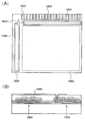
도 6(A) 및 도 6(B)는, 발광 표시 패널의 일 예를 나타낸 평면도 및 단면도이다.
도 7은, 표시 장치의 블럭도의 일 예를 나타낸 도면이다.
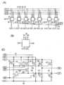
도 8은, 구동 회로의 일 예를 나타낸 도면이다.
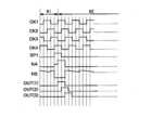
도 9는, 구동 회로의 타이밍 차트를 나타낸 도면이다.
도 10(A) 내지 도 10(C)는, 구동 회로의 일 예를 나타낸 도면이다.
도 11(A) 내지 도 11(D)는, 구동 회로에 공급되는 신호의 공급 및 정지 순서의 일 예를 나타낸 도면이다.
도 12(A) 및 도 12(B)는, 발광 표시 패널의 일 예를 나타낸 평면도 및 단면도이다.
도 13(A) 및 도 12(B)는, 트랜지스터의 일 예를 나타낸 평면도 및 단면도이다.
도 14(A) 내지 도 14(E)는, 트랜지스터의 제작 방법의 일 예를 나타낸 단면도이다.
도 15(A) 내지 도 15(E)는, 트랜지스터의 제작 방법의 일 예를 나타낸 단면도이다.
도 16(A) 내지 도 16(D)는, 트랜지스터의 제작 방법의 일 예를 나타낸 단면도이다.
도 17(A) 내지 도 17(D)는, 트랜지스터의 제작 방법의 일 예를 나타낸 단면도이다.
도 18은, 화소 구성의 일 예를 나타낸 단면도이다.
도 19(A) 내지 도 19(C)는, 전자 기기를 나타낸 도면이다.
도 20은, 전자 기기를 나타낸 도면이다.
도 21은, 산화물 반도체를 이용한 MOS 트랜지스터의 소스-드레인 간 밴드구조를 나타낸 도면이다.
도 22는, 도 19에서 드레인 측으로 플러스 전압이 인가된 상태를 나타낸 도면이다.
도 23(A) 및 도 23(B)는 산화물 반도체를 이용한 MOS 트랜지스터의 MOS 구조의 에너지밴드도이고, (A) 게이트 전압을 플러스로 한 경우, (B) 게이트 전압을 마이너스로 한 경우를 나타낸 도면이다.
도 24는, 실리콘 MOS 트랜지스터의 소스-드레인 간 밴드구조를 나타낸 도면이다.
도 25는, 제작한 트랜지스터의 초기 특성을 나타낸 도면이다.
도 26(A) 및 도 26(B)는, 제작한 트랜지스터를 나타낸 상면도이다.
도 27(A) 및 도 27(B)는, 제작한 트랜지스터의 전기 특성을 나타낸 도면이다.
도 28은, 구동 회로에 공급되는 신호의 공급 및 정지 순서의 일 예를 나타낸 도면이다.1 is a diagram illustrating an example of a configuration of a display device.
2 is an equivalent circuit diagram illustrating an example of a pixel configuration.
3 is a cross-sectional view illustrating an example of a transistor.
4 is a diagram showing the relationship between a write period and a sustain period for a pixel.
5(A) to 5(C) are cross-sectional views illustrating an example of a pixel configuration.
6A and 6B are a plan view and a cross-sectional view illustrating an example of a light emitting display panel.
7 is a diagram illustrating an example of a block diagram of a display device.
8 is a diagram illustrating an example of a driving circuit.
Fig. 9 is a diagram showing a timing chart of the driving circuit.
10A to 10C are diagrams illustrating an example of a driving circuit.
11(A) to 11(D) are diagrams showing an example of a sequence of supplying and stopping a signal supplied to a driving circuit.
12A and 12B are a plan view and a cross-sectional view illustrating an example of a light emitting display panel.
13A and 12B are a plan view and a cross-sectional view illustrating an example of a transistor.
14A to 14E are cross-sectional views illustrating an example of a method for manufacturing a transistor.
15A to 15E are cross-sectional views showing an example of a method for manufacturing a transistor.
16A to 16D are cross-sectional views illustrating an example of a method for manufacturing a transistor.
17A to 17D are cross-sectional views illustrating an example of a method for manufacturing a transistor.
18 is a cross-sectional view showing an example of a pixel configuration.
19(A) to 19(C) are diagrams showing an electronic device.
20 is a diagram illustrating an electronic device.
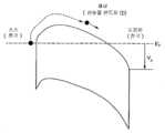
21 is a diagram showing a source-drain band structure of a MOS transistor using an oxide semiconductor.
22 is a diagram illustrating a state in which a positive voltage is applied to the drain side in FIG. 19 .
23(A) and 23(B) are energy band diagrams of a MOS structure of a MOS transistor using an oxide semiconductor, (A) when the gate voltage is positive and (B) when the gate voltage is negative. It is a drawing.
24 is a diagram showing a source-drain band structure of a silicon MOS transistor.
25 is a diagram showing the initial characteristics of the fabricated transistor.
26(A) and 26(B) are top views showing a fabricated transistor.
27(A) and 27(B) are diagrams showing electrical characteristics of the fabricated transistor.
28 is a diagram showing an example of a sequence of supplying and stopping a signal supplied to a driving circuit.
본 발명의 일 양태에 관한 실시형태에 대해, 도면을 이용하여 자세히 설명한다. 단, 본 발명은 이하의 설명에 한정되지 않으며, 본 발명의 취지 및 그 범위에서 벗어나지 않는 한도 내에서 그 형태 및 상세한 내용을 다양하게 변경할 수 있는 것은 당업자라면 용이하게 이해할 수 있다. 따라서, 실시형태의 기재 내용에 한정하여 해석되어서는 안 된다. 한편, 이하에 설명하는 본 발명의 일 양태에서, 동일한 것을 나타내는 부호는 다른 도면에서도 공통으로 한다.EMBODIMENT OF THE INVENTION Embodiment which concerns on one aspect of this invention is described in detail using drawings. However, the present invention is not limited to the following description, and it can be easily understood by those skilled in the art that various changes can be made in form and detail within the limits that do not depart from the spirit and scope of the present invention. Therefore, it should not be interpreted limited to the description of embodiment. On the other hand, in one aspect of the present invention described below, reference numerals indicating the same are common to other drawings.
한편, 이하에 설명하는 실시형태 및 실시예의 각각에서, 특별히 언급이 없는 한, 본 명세서에 기재되어 있는 다른 실시형태 및 실시예와 적절히 조합하여 실시하는 것이 가능하다.In addition, in each of the embodiment and Example described below, it is possible to carry out suitably combining with other embodiment and Example described in this specification, unless there is special notice.
(실시형태 1)(Embodiment 1)
본 실시형태에서는, 본 발명의 일 양태인 표시 장치의 일 예에 대해 설명한다. 특히, 표시 장치의 화소부에 형성되는 화소 구성의 일 예에 대해 도 1, 도 2, 도 3, 도 4, 도 5(A) 내지 도 5(C), 도 6(A) 및 도 6(B)를 이용하여 설명한다.In this embodiment, an example of a display device which is an aspect of the present invention will be described. In particular, FIGS. 1, 2, 3, 4, 5 (A) to 5 (C), 6 (A) and 6 ( B) is used to explain.
도 1은, 본 발명의 일 양태인 표시 장치의 구성의 일 예를 나타낸 도면이다. 도 1에 나타낸 바와 같이, 표시 장치에는, 복수의 화소(201)가 매트릭스 형태로 배치된 화소부(202)가 기판(200) 위에 형성되어 있다. 그리고, 표시 장치는, 복수의 화소(201)를 구동하는 회로로, 주사선 구동 회로(203) 및 신호선 구동 회로(204)를 갖는다. 화소(201)는, 주사선 구동 회로(203)에 전기적으로 접속된 제 1 배선(121)(주사선)에 의해 공급되는 주사 신호에 의해, 각 행 별로 선택 상태인지, 비 선택 상태인지가 결정된다. 또한, 주사 신호에 의해 선택되어 있는 화소(201)는, 신호선 구동 회로(204)에 전기적으로 접속된 제 2 배선(122)(신호선)에 의해, 제 2 배선(122)에서 비디오 전압(영상 신호, 화상 신호, 비디오 신호, 비디오 데이터라고도 한다. )이 공급된다. 또한, 화소(201)에는 한 쌍의 전극을 갖는 발광 소자가 형성되어 있고, 이 발광 소자의 한쪽 전극에는 전위를 공급하기 위한 전원선(123)이 전기적으로 접속되어 있다.1 is a diagram illustrating an example of the configuration of a display device according to an embodiment of the present invention. As shown in FIG. 1 , in the display device, a
한편, 도 1에서는, 주사선 구동 회로(203), 및 신호선 구동 회로(204)가 기판(200) 위에 형성되는 구성에 대해 도시하고 있으나, 본 발명은 이 구성에 한정되지 않는다. 즉, 주사선 구동 회로(203) 또는 신호선 구동 회로(204) 중 어느 한쪽이 기판(200) 위에 형성되는 구성이어도 좋다. 또한, 화소부(202) 만이 기판(200) 위에 형성되는 구성이어도 좋다.On the other hand, although FIG. 1 shows a configuration in which the scan
또한, 도 1에서는, 복수의 화소(201)가 매트릭스 형태로 배치(스트라이프 배치)되어 있는 예를 나타내고 있으나, 본 발명은 이 구성에 한정되지 않는다. 즉, 화소(201)의 배치 구성으로, 스트라이프 배치뿐만 아니라, 델타 배치, 베이어 배치 등을 채용할 수 있다.1 shows an example in which a plurality of
또한, 화소부(202)에서의 표시 방식은, 프로그레시브 방식이나 인터레스 방식 등을 이용할 수 있다. 또한, 컬러 표시할 때에 화소에서 제어하는 색 요소로는, RGB(R은 적, G는 녹, B는 청을 나타낸다.)의 삼색에 한정되지 않는다. 예를 들어, RGBW(W는 백을 나타낸다.), 또는 RGB에, 옐로우, 시안, 마젠타 등을 한가지 색 이상 추가한 것이 있다. 한편, 색 요소의 도트 별로 그 표시 영역의 크기가 달라도 좋다. 단, 본 발명은 컬러 표시의 표시 장치에 한정되는 것이 아니며, 흑백 표시 장치에 적용할 수도 있다.In addition, as the display method in the
또한, 도 1에서, 제 1 배선(121) 및 제 2 배선(122)의 갯수가, 각각 화소의 행 방향 및 열 방향의 수에 1 대 1로 대응한 것을 나타내고 있으나, 본 발명은 이 구성에 한정되지 않는다. 예를 들어, 이웃하는 화소간에, 제 1 배선(121) 또는 제 2 배선(122)을 공유하여 화소(201)를 구동하는 구성으로 하여도 좋다.1 shows that the number of the
도 2는, 도 1에서의 화소(201) 구성의 일 예를 나타낸 등가 회로도이다. 한편, 본 발명은 도 2에 나타낸 화소 구성에 한정되는 것은 아니다.FIG. 2 is an equivalent circuit diagram illustrating an example of the configuration of the
화소(6400)에는, 제 1 트랜지스터(이하, 스위칭용 트랜지스터라고 부를 수 있다.)(6401)와, 제 2 트랜지스터(이하, 구동용 트랜지스터라고 부를 수 있다.)(6402)와, 발광 소자(6404)가 형성되어 있다.In the
제 1 트랜지스터(6401)는, 게이트가 주사선(6406)에 전기적으로 접속되고, 제 1 전극(소스 전극 및 드레인 전극의 한쪽)이 신호선(6405)에 전기적으로 접속되고, 제 2 전극(소스 전극 및 드레인 전극의 다른 한쪽)이 제 2 트랜지스터(6402)의 게이트에 전기적으로 접속되어 있다. 또한, 제 2 트랜지스터(6402)는, 제 1 전극(소스 전극 및 드레인 전극의 한쪽)이 전원선(6407)에 전기적으로 접속되고, 제 2 전극(소스 전극 및 드레인 전극의 다른 한쪽)이 발광 소자(6404)의 제 1 전극(화소전극)에 전기적으로 접속되어 있다. 한편, 발광 소자(6404)의 제 2 전극은 공통 전극(6408)에 상응한다. 또한, 도 2에서는 제 2 트랜지스터(6402)의 게이트와 전원선(6407) 사이에 용량 소자(6410)를 형성하는 구성으로 하였으나, 본 발명은 이 구성에 한정되지 않는다. 예를 들어, 제 2 트랜지스터(6402)의 게이트와 제 2 트랜지스터(6402)의 제 2 전극 사이에 용량 소자를 형성하는 구성으로 하여도 좋다.The
공통 전극(6408)은, 공통 전위선과 전기적으로 접속되고, 저전원 전위가 공급되도록 설정되어 있다. 또한, 전원선(6407)에는 고전원 전위가 공급되도록 설정되어 있다. 한편, 저전원 전위란, 전원선(6407)에 설정되는 고전원 전위를 기준으로 하여 저전원 전위<고전원 전위를 만족하는 전위이다. 저전원 전위의 구체예로는, GND, 0V를 들 수 있다. 한편, 고전원 전위와 저전원 전위의 전위는, 고전원 전위와 저전원 전위의 전위 차가 적어도 발광 소자(6404)의 순방향 역치 전압 이상이 되도록 각각 설정할 필요가 있다.The
여기서, 본 실시형태에서는, 산화물 반도체층을 갖는 트랜지스터를 제 1 트랜지스터(6401)로 이용하고 있다. 이때, 제 1 트랜지스터(6401)는 n 채널형 트랜지스터이다. 또한, 제 2 트랜지스터(6402)는, n 채널형 트랜지스터 및 p 채널형 트랜지스터 중 어느 쪽을 이용하여도 좋다. 또한, 제 2 트랜지스터(6402)는, 활성층으로 산화물 반도체층을 이용한 구성으로 하여도 좋으며, 실리콘층을 이용한 구성으로 하여도 좋다. 활성층으로 실리콘층을 이용하는 경우는, 비정질의 실리콘층이어도 좋으나, 다결정의 실리콘층을 이용하는 것이 바람직하다. 본 실시형태에서는, 제 2 트랜지스터(6402)가 n 채널형 트랜지스터이고, 산화물 반도체층을 활성층으로 이용하는 경우에 대해 설명한다.Here, in the present embodiment, a transistor having an oxide semiconductor layer is used as the
이어서, 화소(6400)에서의 제 1 트랜지스터(6401)의 단면도의 일 예를 도 3에 나타낸다. 도 3에 나타낸 트랜지스터(106)는, 제 1 트랜지스터(6401)에 대응하는 것으로, 보톰 게이트형의 구조이다. 또한, 채널 영역이 되는 산화물 반도체층(103)에 대해 아래측으로 게이트 전극으로 기능하는 제 1 배선(101)을 갖고, 산화물 반도체층(103)을 사이에 끼워 제 1 배선(101)과 반대측에, 제 1 전극(소스 전극 및 드레인 전극의 한쪽)(102A), 및 제 2 전극(소스 전극 및 드레인 전극의 다른 한쪽)(102B)을 가지므로, 역스태거형의 트랜지스터라고도 불린다.Next, an example of a cross-sectional view of the
기판(111) 위에는, 하지막(112)을 통해 제 1 배선(101)이 형성되어 있다. 제 1 배선(101)은, 트랜지스터(106)의 게이트로 기능한다. 그리고, 제 1 배선(101)은, 주사선 구동 회로와 전기적으로 접속되는 주사선 그 자체이어도 좋으며, 주사선과 전기적으로 접속되어 있는 배선이어도 좋다.A
또한, 제 1 배선(101)을 덮도록 게이트 절연막(113)이 형성되어 있다. 그리고, 게이트 절연막(113) 위에는 산화물 반도체층(103)이 형성되어 있다. 그리고, 산화물 반도체층(103) 위에는, 제 1 전극(102A), 및 제 2 전극(102B)이 형성되어 있다. 제 1 전극(102A), 및 제 2 전극(102B)은, 산화물 반도체층(103)에 전기적으로 접속되어 있고, 한쪽이 소스 전극으로 기능하고, 다른 한쪽이 드레인 전극으로 기능한다. 한편, 제 1 전극(102A)은, 신호선 구동 회로와 전기적으로 접속되는 신호선 그 자체이어도 좋으며, 신호선과 전기적으로 접속되어 있는 배선이어도 좋다.In addition, a
또한, 산화물 반도체층(103), 제 1 전극(102A), 및 제 2 전극(102B) 위에는, 패시베이션막으로 기능하는 산화물 절연층(114)이 형성되어 있다. 산화물 절연층(114)에는 개구부가 형성되어 있고, 이 개구부에서 제 4 배선(105)과 제 2 전극(102B)이 전기적으로 접속되어 있다. 한편, 이 제 4 배선(105)은, 제 2 트랜지스터의 게이트에 전기적으로 접속되어 있다.Further, an
이어서, 산화물 반도체층(103)에 대해 설명한다.Next, the
본 실시형태에서 이용하는 산화물 반도체층(103)은, 산화물 반도체를 이용한 트랜지스터의 전기 특성에 악영향을 주는 불순물이 매우 적은 레벨까지 저감된 것으로, 고순도화된 것이다. 전기 특성에 악영향을 주는 불순물의 대표적인 예로는, 수소를 들 수 있다. 수소는, 산화물 반도체 중에서 전자의 공여체(도너)가 될 수 있는 불순물이고, 산화물 반도체 중에 수소가 다량으로 포함되어 있으면, 산화물 반도체가 N형화되게 된다. 이와 같이 수소가 다량으로 포함된 산화물 반도체를 이용한 트랜지스터는, 노멀리 온 되게 된다. 그리고, 트랜지스터의 온·오프 비를 충분히 가질 수 없게 된다. 따라서, 본 명세서에서의 '고순도의 산화물 반도체'는 산화물 반도체에서의 수소가 최대한 저감되어 있는 것으로, 진성 또는 실질적으로 진성인 반도체를 말한다. 고순도의 산화물 반도체의 일 예로는, 함유하는 수소 농도가 적어도 5×10¹⁹/cm3 이하로, 바람직하게는 5×10¹⁸/cm3 이하, 더욱 바람직하게는 5×10¹⁷/cm3 이하, 또는 1×10¹⁶/cm3 미만인 산화물 반도체이다. 그리고, 캐리어 농도가, 1×10¹⁴/cm3 미만, 바람직하게는 1×10¹²/cm3 미만, 더욱 바람직하게는 1×10¹¹/cm3 미만, 또는 6.0×10¹⁰/cm3 미만인 산화물 반도체막을 채널 형성 영역에 이용하여 트랜지스터를 구성한다. 한편, 산화물 반도체층 중의 수소 농도 측정은, 이차이온 질량 분석법(SIMS: Secondary Ion Mass Spectroscopy)으로 행하면 된다.In the
또한, 산화물 반도체층(103)의 에너지갭는, 2eV 이상, 바람직하게는 2.5eV 이상, 보다 바람직하게는 3eV 이상이다.Moreover, the energy gap of the
이와 같이, 산화물 반도체층에 포함되는 수소를 철저히 제거함으로써 얻어지는 고순도의 산화물 반도체층을 트랜지스터의 채널 형성 영역으로 이용함으로써, 오프 전류 값이 매우 작은 트랜지스터를 제공할 수 있다.As described above, by using the high-purity oxide semiconductor layer obtained by thoroughly removing hydrogen contained in the oxide semiconductor layer as the channel formation region of the transistor, it is possible to provide a transistor with a very small off-state current value.
예를 들어, 고순도의 산화물 반도체층을 이용한 트랜지스터의 채널 길이가 3㎛, 채널 폭이 10mm인 경우에도, 드레인 전압이 1V 및 10V인 경우에서, 게이트 전압이 -5V에서 -20V인 범위(오프 상태)에서, 드레인 전류는 1×10-13A 이하가 되도록 작용한다.For example, even when a transistor using a high-purity oxide semiconductor layer has a channel length of 3 μm and a channel width of 10 mm, when the drain voltages are 1V and 10V, the gate voltage is in the range of -5V to -20V (off state). ), the drain currentacts to be 1×10 -13 A or less.
여기서, 고순도의 산화물 반도체층을 이용한 트랜지스터의 특성에 대해, 도 21 내지 도 27을 이용하여 설명한다. 한편, 이하의 설명에서는, 이해를 쉽게 하기 위해 이상적인 상황을 가정하고 있으며, 모든 것이 현실의 모양을 반영하고 있다고는 할 수 없다. 또한, 이하의 설명은 어디까지나 하나의 고찰에 지나지 않으며, 발명의 유효성에 영향을 주는 것이 아님을 명시한다.Here, characteristics of a transistor using a high-purity oxide semiconductor layer will be described with reference to FIGS. 21 to 27 . On the other hand, in the following description, an ideal situation is assumed for easy understanding, and it cannot be said that everything reflects the shape of reality. In addition, it is specified that the following description is merely a consideration, and does not affect the effectiveness of the invention.
도 21은, 고순도의 산화물 반도체층을 이용한 트랜지스터의 소스-드레인 간 밴드 구조를 나타낸 도면이다. 고순도화가 얻어진 산화물 반도체의 페르미 준위는, 이상적인 상태에서는 금제대의 중앙에 위치하고 있다. 수소 농도를 감소시킨 산화물 반도체에서는 소수 캐리어(이 경우는 정공)가 0(zero) 또는 무한대로 0에 가까운 상태로 되어 있다.21 is a diagram illustrating a source-drain band structure of a transistor using a high-purity oxide semiconductor layer. The Fermi level of the oxide semiconductor obtained with high purity is located at the center of the forbidden band in an ideal state. In an oxide semiconductor in which the hydrogen concentration is reduced, minority carriers (holes in this case) are in a state of zero or infinitely close to zero.
이 경우, 일함수를 φm, 산화물 반도체의 전자 친화력을 χ, 산화물 반도체의 열평형 상태에서의 캐리어 밀도(전자 밀도)를 Nd, 산화물 반도체의 전도대에서의 실효 상태 밀도를 Nc로 하면, 금속-산화물 반도체의 접합면에서 밴드 구조가 플랫이 되기 위한 조건은, φm=χ-Vtln(Nd/Nc)가 된다.In this case, if the work function is φm , the electron affinity of the oxide semiconductor is χ , the carrier density (electron density) in the thermal equilibrium state of theoxide semiconductor is N d , and the effective state density in the conduction band of the oxide semiconductor is Nc , The condition for the band structure to be flat at the junction surface of the metal-oxide semiconductor is phim = χ-Vt ln(Nd /Nc ).
여기서, Vt=kbT/q이고, kb:볼츠만 상수, T:온도, q:소전하이다. 이 등식 φm=χ-Vtln(Nd/Nc)을 경계로, 우변이 큰 경우는 오믹 접촉이 된다. 여기서, φm=χ이면, 접합면에서 전극 메탈의 페르미 레벨과 산화물 반도체의 전도대의 레벨이 일치한다. 산화물 반도체는, 밴드갭 3.05eV, 전자 친화력 4.3eV, 진성 상태(캐리어 밀도 약 1×10⁻⁷/cm3)이라고 가정하고, 소스 전극 및 드레인 전극으로 일함수 4.3eV의 티탄(Ti)을 이용했을 때에는, 도 21에 나타낸 바와 같이 전자에 대해 격벽은 형성되지 않는다.Here, Vt =kb T/q, kb : Boltzmann constant, T: temperature, q: small charge. Based on this equation φm =χ-Vt ln(Nd /Nc ), when the right side is large, it is an ohmic contact. Here, when phim = χ, the Fermi level of the electrode metal and the level of the conduction band of the oxide semiconductor coincide with each other at the junction surface. Assuming that the oxide semiconductor has a band gap of 3.05 eV, an electron affinity of 4.3 eV, and an intrinsic state (carrier density of about 1×10⁻⁷ /cm3 ), titanium (Ti) with a work function of 4.3 eV is used as the source electrode and the drain electrode. In this case, as shown in FIG. 21, the barrier rib is not formed with respect to the former.
도 22는 산화물 반도체를 이용한 트랜지스터에서, 드레인 측으로 플러스 전압이 인가된 상태를 나타낸 도면이다. 산화물 반도체는 밴드갭이 크므로, 고순도화되고 진성 또는 실질적으로 진성인 산화물 반도체의 진성 캐리어 밀도는 0 또는 무한대로 0에 가까운 상태이나, 게이트에 플러스 전압을 인가하고, 또한, 소스-드레인 간에 전압이 인가되면, 소스 측에서 캐리어(전자)가 주입되고, 드레인 측으로 흐를 수 있는 것을 이해할 수 있다.22 is a diagram illustrating a state in which a positive voltage is applied to a drain side of a transistor using an oxide semiconductor. Since the oxide semiconductor has a large bandgap, the intrinsic carrier density of a highly purified and intrinsic or substantially intrinsic oxide semiconductor is zero or infinitely close to zero, but a positive voltage is applied to the gate, and a voltage between the source and drain When this is applied, it can be understood that carriers (electrons) are injected from the source side and can flow to the drain side.
도 23(A)는 게이트 전압을 플러스로 했을 때의 MOS 구조의 에너지밴드도이고, 산화물 반도체를 이용한 트랜지스터에서의 것을 나타내고 있다. 한편, 도면에서 GE는 게이트 전극을 나타내고, GI는 게이트 절연막을 나타내고, OS는 산화물 반도체를 나타낸다. 이 경우, 고순도화된 산화물 반도체에는 열여기 캐리어가 거의 존재하지 않는다는 점에서, 게이트 절연막 부근에도 캐리어는 축적되지 않는다. 그러나, 도 22에 나타낸 바와 같이, 소스 측에서 주입된 캐리어가 전파될 수는 있다.Fig. 23A is an energy band diagram of the MOS structure when the gate voltage is positive, and shows the transistor using an oxide semiconductor. Meanwhile, in the drawings, GE denotes a gate electrode, GI denotes a gate insulating film, and OS denotes an oxide semiconductor. In this case, since there are almost no thermally excited carriers in the highly purified oxide semiconductor, carriers do not accumulate even in the vicinity of the gate insulating film. However, as shown in FIG. 22 , carriers injected from the source side may propagate.
도 23(B)는, 게이트 전압을 마이너스로 했을 때의 MOS 구조의 에너지밴드도이고, 산화물 반도체를 이용한 트랜지스터에서의 것을 나타내고 있다. 산화물 반도체 중의 소수 캐리어(정공)는 실질적으로 0이므로, 소스-드레인 간 전류는 무한대로 0에 가까운 값이 된다.Fig. 23B is an energy band diagram of the MOS structure when the gate voltage is negative, and shows the transistor using an oxide semiconductor. Since minority carriers (holes) in the oxide semiconductor are substantially zero, the source-drain current becomes infinitely close to zero.
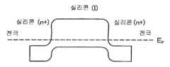
한편, 도 24에 실리콘 반도체를 이용한 경우의 트랜지스터의 밴드도를 나타낸다. 실리콘 반도체의 진성 캐리어 밀도는 1.45×10¹⁰/cm3(300K)이고, 실온에서도 캐리어가 존재하고 있다. 이는, 실온에서도, 열여기 캐리어가 존재하고 있다는 것을 의미한다. 실용적으로는 인 또는 보론 등의 불순물이 첨가된 실리콘 웨이퍼가 사용되므로, 실제로는 1×10¹⁴/cm3 이상의 캐리어가 실리콘 반도체에 존재하고, 이것이 소스-드레인 간 전도에 기여한다. 나아가, 실리콘 반도체의 밴드갭은 1.12eV이므로, 실리콘 반도체를 이용한 트랜지스터는 온도에 의존하여 오프 전류가 크게 변동하게 된다.On the other hand, Fig. 24 shows a band diagram of a transistor in the case of using a silicon semiconductor. The intrinsic carrier density of a silicon semiconductor is 1.45×10¹⁰ /cm3 (300K), and carriers exist even at room temperature. This means that even at room temperature, thermal excitation carriers are present. Since a silicon wafer doped with impurities such as phosphorus or boron is used practically,carriers of 1×10 14 /cm3 or more actually exist in the silicon semiconductor, which contributes to source-drain conduction. Furthermore, since the band gap of the silicon semiconductor is 1.12 eV, the off current of the transistor using the silicon semiconductor varies greatly depending on the temperature.
이와 같이, 단순히, 밴드갭이 넓은 산화물 반도체를 트랜지스터에 적용하는 것이 아니라, 도너를 형성하는 수소 등의 불순물을 최대한 저감하고, 캐리어 농도를 1×10¹⁴/cm3 미만, 바람직하게는 1×10¹²/cm3 미만, 더욱 바람직하게는 1×10¹¹/cm3 미만, 또는 6.0×10¹⁰/cm3 미만이 되도록 함으로써, 실용적인 동작 온도에서 열적으로 여기되는 캐리어를 배제하여, 소스 측에서 주입되는 캐리어만에 의해 트랜지스터를 동작시킬 수 있다. 이에 의해, 오프 전류를 1×10-13A 이하까지 낮춤과 동시에, 온도 변화에 의해 오프 전류가 거의 변화하지 않는 매우 안정적으로 동작하는 트랜지스터를 얻을 수 있다.As described above, rather than simply applying an oxide semiconductor having a wide bandgap to the transistor, impurities such as hydrogen forming a donor are reduced as much as possible, and the carrier concentration is reduced toless than 1×10 14 /cm3 , preferably 1×10less than 12 /cm3 , more preferably less than 1×10¹¹ /cm3 , or less than 6.0×10¹⁰ /cm3 , thereby excluding thermally excited carriers at practical operating temperatures, and Transistors can be operated only by carriers. In this way, it is possible to obtain a transistor that reduces the off current to 1×10-13 A or less and operates very stably with little change in the off current due to temperature change.
이어서, 평가용 소자(TEG라고도 한다)에서의 오프 전류의 측정치에 대해 이하에 설명한다.Next, the measured value of the off current in the element for evaluation (also referred to as TEG) will be described below.
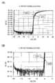
L/W=3㎛/50㎛의 트랜지스터를 200개 병렬로 접속하고, L/W=3㎛/10000㎛의 트랜지스터의 초기 특성을 도 25에 나타낸다. 여기에서는, Vg를 -20V~+5V까지의 범위로 나타내고 있다. 또한, 상면도를 도 26(A)에 나타내고, 그 일부를 확대한 상면도를 도 26(B)에 나타낸다. 도 26(B)의 점선으로 둘러싼 영역이 L/W=3㎛/50㎛, Lov=1.5㎛의 1단 분의 트랜지스터이다. 트랜지스터의 초기 특성을 측정하기 위해, 기판 온도를 실온으로 하고, 소스-드레인 간 전압(이하, 드레인 전압 또는 Vd라 한다.)을 10V로 하고, 소스-게이트 간 전압(이하, 게이트 전압 또는 Vg라 한다.)을 -20V~+20V까지 변화시켰을 때의 소스-드레인 전류(이하, 드레인 전류 또는 Id라 한다.)의 변화 특성, 즉 Vg-Id 특성을 측정하였다.200 transistors with L/W = 3 mu m/50 mu m are connected in parallel, and the initial characteristics of the transistors with L/W = 3 mu m/10000 mu m are shown in FIG. 25 . Here, Vg is shown in the range of -20V to +5V. In addition, a top view is shown in FIG.26(A), and the top view which expanded the part is shown in FIG.26(B). A region surrounded by a dotted line in Fig. 26B is a transistor for one stage with L/W = 3 mu m/50 mu m and Lov = 1.5 mu m. In order to measure the initial characteristics of the transistor, the substrate temperature is at room temperature, the source-drain voltage (hereinafter referred to as drain voltage or Vd) is 10 V, and the source-gate voltage (hereinafter referred to as gate voltage or Vg) is assumed to be 10 V. The change characteristics of the source-drain current (hereinafter referred to as drain current or Id) when the voltage is changed from -20V to +20V, that is, the Vg-Id characteristic, was measured.
도 25에 나타낸 바와 같이, 채널 폭(W)이 10000㎛인 트랜지스터는, Vd가 1V 및 10V에서 오프 전류는 1×10-13[A] 이하로 되어 있고, 측정기(반도체 파라메터·아날라이저, Agilent 4156C; Agilent사 제조)의 분해능(100fA) 이하로 되어 있다.As shown in Fig. 25, in a transistor with a channel width (W) of 10000 µm, when Vd is 1 V and 10 V, the off current is 1 × 10-13 [A] or less, and a measuring instrument (semiconductor parameter analyzer, Agilent 4156C) The resolution (100 fA) of Agilent Co., Ltd. or less is set.
이어서, 측정한 트랜지스터의 제작 방법에 대해 설명한다.Next, the manufacturing method of the measured transistor is demonstrated.
우선, 유리 기판 위에 하지층으로, CVD법에 의해 질화 규소층을 형성하고, 질화 규소층 위에 산화질화 규소층을 형성하였다. 산화질화 규소층 위에 게이트 전극으로 스퍼터링법에 의해 텅스텐층을 형성하였다. 여기서, 텅스텐층을 선택적으로 에칭하여 게이트 전극을 형성하였다.First, a silicon nitride layer was formed by the CVD method as a base layer on a glass substrate, and a silicon oxynitride layer was formed on the silicon nitride layer. A tungsten layer was formed on the silicon oxynitride layer by sputtering as a gate electrode. Here, the tungsten layer was selectively etched to form a gate electrode.
이어서, 게이트 전극 위에 게이트 절연층으로 CVD법에 의해 두께 100nm의 산화질화 규소층을 형성하였다.Then, a silicon oxynitride layer having a thickness of 100 nm was formed on the gate electrode by the CVD method as a gate insulating layer.
이어서, 게이트 절연층 위에, 스퍼터링법에 의해 In-Ga-Zn-O계의 금속 산화물 타겟(몰수비로, In2O3:Ga2O3:ZnO=1:1:2)을 이용하여, 두께 50nm의 산화물 반도체층을 형성하였다. 그리고, 산화물 반도체층을 선택적으로 에칭하여, 섬 모양의 산화물 반도체층을 형성하였다.Next, on the gate insulating layer, an In-Ga-Zn-O-based metal oxide target (in mole ratio, In2 O3 :Ga2 O3 :ZnO=1:1:2) was used by sputtering to obtain a thickness A 50 nm oxide semiconductor layer was formed. Then, the oxide semiconductor layer was selectively etched to form an island-shaped oxide semiconductor layer.
이어서, 산화물 반도체층을 클린 오븐에서 질소 분위기 하, 450℃, 1시간의 제 1 열처리를 하였다.Next, the oxide semiconductor layer was subjected to a first heat treatment at 450° C. for 1 hour in a nitrogen atmosphere in a clean oven.
이어서, 산화물 반도체층 위에 소스 전극 및 드레인 전극으로 티탄층(두께 150nm)을 스퍼터링법에 의해 형성하였다. 여기서, 소스 전극 및 드레인 전극을 선택적으로 에칭하고, 1개의 트랜지스터의 채널 길이(L)가 3㎛, 채널 폭(W)이 50㎛로 하고, 200개를 병렬로 함으로써, L/W=3㎛/10000㎛가 되도록 하였다.Next, a titanium layer (thickness 150 nm) was formed as a source electrode and a drain electrode on the oxide semiconductor layer by sputtering. Here, the source electrode and the drain electrode are selectively etched, the channel length (L) of one transistor is 3 µm, the channel width (W) is 50 µm, and 200 are parallel to each other, so that L/W = 3 µm It was made to become 100000 micrometers.
이어서, 산화물 반도체층에 접하도록 보호 절연층으로 리액티브 스퍼터링법에 의해 산화 규소층을 막후 300nm로 형성하였다. 여기서, 보호 절연층인 산화 규소층을 선택적으로 에칭하고, 게이트 전극, 소스 전극 및 드레인 전극 위에 개구부를 형성하였다. 그 후, 질소 분위기 하, 250℃에서 1시간, 제 2 열처리를 하였다.Then, a silicon oxide layer was formed to a thickness of 300 nm by reactive sputtering as a protective insulating layer so as to be in contact with the oxide semiconductor layer. Here, the silicon oxide layer as the protective insulating layer was selectively etched to form openings over the gate electrode, the source electrode, and the drain electrode. Thereafter, a second heat treatment was performed at 250° C. for 1 hour in a nitrogen atmosphere.
그리고, Vg-Id 특성을 측정하기 전에 150℃, 10시간의 가열을 하였다.Then, before measuring the Vg-Id characteristics, heating was performed at 150° C. for 10 hours.
이상의 공정에 의해, 보톰 게이트형의 트랜지스터를 제작하였다.Through the above steps, a bottom gate type transistor was produced.
도 25에 나타낸 바와 같이, 트랜지스터의 오프 전류가, 1×10-13[A] 정도인 것은, 상기 제작 공정에서 산화물 반도체층 중에서의 수소 농도를 충분히 저감할 수 있었기 때문이다. 산화물 반도체층 중의 수소 농도는, 5×10¹⁹atoms/cm3 이하, 바람직하게는 5×10¹⁸atoms/cm3 이하, 더욱 바람직하게는 5×10¹⁷/cm3 이하, 또는 1×10¹⁶atoms/cm3 미만으로 한다. 한편, 산화물 반도체층 중의 수소 농도 측정은, 이차이온 질량 분석법(SIMS: Secondary Ion Mass Spectroscopy)으로 행한다.As shown in FIG. 25 , the off current of the transistor isabout 1×10 −13 [A] because the hydrogen concentration in the oxide semiconductor layer can be sufficiently reduced in the manufacturing process. The hydrogen concentration in the oxide semiconductor layer is 5×10¹⁹ atoms/cm3 or less, preferably 5×10¹⁸ atoms/cm3 or less, more preferably 5×10¹⁷ /cm3 or less, or 1×10¹⁶ atoms /cm3 or less. In addition, the hydrogen concentration measurement in an oxide semiconductor layer is performed by secondary ion mass spectroscopy (SIMS:Secondary Ion Mass Spectroscopy).
또한, In-Ga-Zn-O계의 산화물 반도체를 이용하는 예를 도시하였으나, 특별히 한정되지 않으며, 다른 산화물 반도체 재료, 예를 들어, In-Sn-Zn-O계, Sn-Ga-Zn-O계, Al-Ga-Zn-O계, Sn-Al-Zn-O계, In-Zn-O계, In-Sn-O계, Sn-Zn-O계, Al-Zn-O계, In-O계, Sn-O계, Zn-O계 등을 이용할 수 있다. 또한, 산화물 반도체 재료로, AlOx를 2.5~10wt% 혼입한 In-Al-Zn-O계나, Si를 2.5~10wt% 혼입한 In-Zn-O계를 이용할 수도 있다.In addition, although an example of using an In-Ga-Zn-O-based oxide semiconductor is shown, it is not particularly limited, and other oxide semiconductor materials, for example, In-Sn-Zn-O-based, Sn-Ga-Zn-O based, Al-Ga-Zn-O, Sn-Al-Zn-O, In-Zn-O, In-Sn-O, Sn-Zn-O, Al-Zn-O, In- O-based, Sn-O-based, Zn-O-based and the like can be used. In addition, as the oxide semiconductor material,an In-Al-Zn-O type containing 2.5 to 10 wt% of AlO x or an In-Zn-O type containing 2.5 to 10 wt% of Si may be used.
또한, 캐리어 측정기로 측정되는 산화물 반도체층의 캐리어 농도는, 1×10¹⁴/cm3 미만, 바람직하게는 1×10¹²/cm3 미만, 더욱 바람직하게는 1×10¹¹/cm3 미만, 또는 6.0×10¹⁰/cm3 미만이다. 즉, 산화물 반도체층의 캐리어 농도는, 무한대로 0에 가깝게 할 수 있다. 한편, 캐리어 농도의 측정 방법의 구체예로는, MOS 캐패시터를 제작하고, 상기 MOS 캐패시터의 CV 측정의 결과(CV 특성)를 평가함으로써 구하는 방법을 들 수 있다.In addition, the carrier concentration of the oxide semiconductor layer measured by a carrier meter isless than 1×10 14 /cm3 , preferably less than 1×10¹² /cm3 , more preferably less than 1×10¹¹ /cm3 , or less than 6.0×10¹⁰ /cm3 . That is, the carrier concentration of the oxide semiconductor layer can be infinitely close to zero. On the other hand, as a specific example of the measuring method of carrier concentration, the method of obtaining by producing a MOS capacitor and evaluating the result (CV characteristic) of the CV measurement of the said MOS capacitor is mentioned.
또한, 트랜지스터의 채널 길이(L)를 10nm 이상 1000nm 이하로 할 수도 있다. 이 경우, 회로의 동작 속도를 고속화할 수 있고, 오프 전류 값이 매우 작으므로, 더욱 저소비 전력화를 도모할 수 있다.In addition, the channel length L of the transistor may be set to 10 nm or more and 1000 nm or less. In this case, the operation speed of the circuit can be increased, and the off current value is very small, so that power consumption can be further reduced.
한편, 트랜지스터의 오프 상태에서, 산화물 반도체층은 절연체로 간주하여 회로 설계를 할 수 있다.On the other hand, in the OFF state of the transistor, the oxide semiconductor layer can be regarded as an insulator and circuit design can be performed.
이어서, 본 실시형태에서 제작한 트랜지스터에 대해 오프 전류의 온도 특성을 평가하였다. 온도 특성은, 트랜지스터가 사용되는 최종 제품의 내환경성이나, 성능의 유지 등을 고려하였을 때 중요하다. 당연히, 변화량이 작을수록 바람직하며, 제품 설계의 자유도가 늘어난다.Next, the temperature characteristic of the off-current was evaluated for the transistor fabricated in this embodiment. The temperature characteristic is important when considering the environmental resistance of the final product in which the transistor is used, and the maintenance of performance. Naturally, it is preferable that the change amount is small, and the degree of freedom in product design is increased.
온도 특성은, 항온조를 이용하여, -30, 0, 25, 40, 60, 80, 100, 및 120℃의 각각의 온도에서 트랜지스터를 형성한 기판을 일정 온도로 하고, 드레인 전압을 6V, 게이트 전압을 -20V~+20V까지 변화시켜 Vg-Id 특성을 취득하였다.As for the temperature characteristics, using a constant temperature bath, the substrate on which the transistor was formed at each temperature of -30, 0, 25, 40, 60, 80, 100, and 120° C. was set to a constant temperature, the drain voltage was 6 V, and the gate voltage was Vg-Id characteristics were obtained by changing from -20V to +20V.
도 27(A)에 나타낸 것은, 상기 각각의 온도에서 측정한 Vg-Id 특성을 중복 기재한 것으로, 점선으로 둘러싼 오프 전류의 영역을 확대한 것을 도 27(B)에 나타낸다. 도에서 화살표로 나타낸 우단의 곡선이 -30℃, 좌단이 120℃에서 취득한 곡선으로, 다른 온도에서 취득한 곡선은, 그 사이에 위치한다. 온 전류의 온도 의존성은 거의 볼 수 없다. 한편, 오프 전류는 확대도인 도 27(B)에서도 알 수 있듯이, 게이트 전압이 -20V 부근을 제외하고, 모든 온도에서 측정기의 분해능 근방의 1×10-12[A] 이하로 되어 있고, 온도 의존성도 보이지 않는다. 즉, 120℃의 고온에서도, 오프 전류가 1×10-12[A] 이하를 유지하고 있으며, 채널 폭(W)이 10000㎛인 것을 고려하면, 1×10-16[A/㎛] 이하가 되고, 오프 전류가 매우 작은 것을 알 수 있다.Fig. 27(A) shows the overlapping description of the Vg-Id characteristics measured at each of the above temperatures, and Fig. 27(B) shows an enlarged area of the off current enclosed by the dotted line. The curve at the right end indicated by an arrow in the figure is a curve obtained at -30°C and the left end is a curve obtained at 120°C, and the curves obtained at different temperatures are located in between. The temperature dependence of the on current is almost invisible.On the other hand, the off current is 1×10 -12 [A] or less in the vicinity of the resolution of the measuring instrument at all temperatures except for the gate voltage around -20 V, and the temperature I don't see any dependencies. That is, even at a high temperature of 120°C, the off current is maintained at 1×10-12 [A] or less, and considering that the channel width (W) is 10000 μm, 1×10-16 [A/μm] or less is and the off current is very small.
고순도화의 산화물 반도체(purified OS)를 이용한 트랜지스터는, 오프 전류의 온도 의존성이 거의 나타나지 않는다. 이는, 도 21의 밴드도에 나타낸 바와 같이, 산화물 반도체가 고순도화됨으로써, 도전형이 무한대로 진성형에 가까워지고, 페르미 준위가 금제대의 중앙에 위치하므로, 온도 의존성을 나타내지 않게 된다고 할 수 있다. 또한, 이는, 산화물 반도체의 에너지갭이 3eV 이상이고, 열여기 캐리어가 매우 적은 것에도 기인한다. 또한, 소스 영역 및 드레인 영역은 축퇴한 상태에 있으므로 역시 온도 의존성이 나타나지 않는 요인이 된다. 트랜지스터의 동작은, 축퇴한 소스 영역에서 산화물 반도체에 주입된 캐리어에 의한 것이 대부분이고, 캐리어 밀도의 온도 의존성이 없다는 점에서 상기 특성(오프 전류의 온도 의존성 없음)을 설명할 수 있다.A transistor using a highly purified oxide semiconductor (purified OS) hardly exhibits temperature dependence of the off current. As shown in the band diagram of FIG. 21, as the oxide semiconductor is highly purified, the conductivity type is infinitely close to the intrinsic type, and since the Fermi level is located at the center of the forbidden band, it can be said that the temperature dependence is not exhibited. . In addition, this is also due to the fact that the energy gap of the oxide semiconductor is 3 eV or more and there are very few thermal excitation carriers. In addition, since the source region and the drain region are in a degenerate state, this also becomes a factor in which temperature dependence does not appear. The operation of the transistor is mostly due to carriers injected into the oxide semiconductor in the degenerate source region, and the above characteristic (no temperature dependence of the off current) can be explained in that there is no temperature dependence of carrier density.
이상과 같이, 트랜지스터의 채널 폭(W)이 1×10⁴㎛이고, 채널 길이가 3㎛인 소자라도, 오프 전류가 10-13A 이하이고, 서브스레숄드 스윙값(S값, subthreshold swing)이 0.1V/dec.(게이트 절연막후 100nm)라는 우수한 전기 특성을 얻을 수 있다. 이와 같이, 산화물 반도체 중의 불순물이 최대한 포함되지 않도록 고순도화함으로써, 트랜지스터의 동작을 양호한 것으로 할 수 있다. 즉, 상술한 산화물 반도체층을 구비하는 트랜지스터는, 채널 폭 1㎛ 당 오프 전류를 10aA/㎛(1×10-17A/㎛)이하, 나아가 1aA/㎛(1×10-18A/㎛) 이하로 하는 것이 가능하다. 그리고, 오프 상태에서의 전류값(오프 전류값)이 매우 작은 트랜지스터를 제 1 트랜지스터(6401)로 이용함으로써, 영상 신호 등의 전기 신호의 유지 시간을 길게 할 수 있다. 예를 들어, 쓰기 간격은 10초 이상, 바람직하게는 30초 이상, 더욱 바람직하게는 1분 이상 10분 미만으로 한다. 쓰기 간격을 길게 함으로써, 소비 전력을 억제하는 효과를 높일 수 있다.As described above, even if the transistor has a channel width W of 1×104 μm and a channel length of 3 μm, the off current is 10-13 A or less, and the subthreshold swing value (S value) is Excellent electrical properties of 0.1 V/dec. (100 nm thickness of the gate insulating film) can be obtained. In this way, by increasing the purity so that impurities in the oxide semiconductor are not contained as much as possible, the operation of the transistor can be improved. That is, the transistor including the oxide semiconductor layer described above has an off current of 10 aA/μm (1×10⁻¹⁷ A/μm) or lessper channel width 1 μm, and further 1 aA/μm (1×10 −18 A/μm) It is possible to do the following. Also, by using a transistor having a very small off-state current value (off-state current value) as the
한편, 예를 들어 저온 폴리 실리콘을 구비하는 트랜지스터에서는, 오프 전류가 1×10-12A/㎛ 상당인 것으로 추정하여 설계 등을 행하도록 되어 있다. 이로 인해, 산화물 반도체를 갖는 트랜지스터에서는, 저온 폴리 실리콘을 구비하는 트랜지스터에 비해, 유지 용량이 동등(0.1pF 정도)할 때, 전압의 유지 기간을 105배 정도 연장할 수 있다. 또한, 아몰퍼스 실리콘을 구비하는 트랜지스터의 경우, 채널 폭 1㎛ 당 오프 전류는, 1×10-13A/㎛ 이상이다. 따라서, 유지 용량이 동등(0.1pF정도)할 때, 고순도의 산화물 반도체를 이용한 트랜지스터가 아몰퍼스 실리콘을 이용한 트랜지스터에 비해, 전압의 유지 기간을 104배 이상 연장할 수 있다.On the other hand, for a transistor including, for example, low-temperature polysilicon, design or the like is performed by estimating that theoff-state current is equivalent to 1×10 -12 A/μm. For this reason, in a transistor including an oxide semiconductor, when the storage capacitance is equal (about 0.1 pF), the voltage holding period can be extended by about10 5 times compared to a transistor including low-temperature polysilicon. Further, in the case of a transistor including amorphous silicon, the off current per channel width of 1 μm is 1×10⁻¹³ A/μm or more. Accordingly, when the holding capacitance is equal (about 0.1 pF), a transistor using a high-purity oxide semiconductor can extend thevoltage holding period 10 4 times or more compared to a transistor using amorphous silicon.
일 예로, 저온 폴리 실리콘을 이용한 트랜지스터를 갖는 화소에서는, 표시를 60프레임/초(1 프레임 당 16msec)로 행하고 있다. 이는 정지화인 경우도 동일하며, 레이트(rate)를 저하시키면(쓰기 간격을 늘림), 화소의 전압이 저하되어 표시에 지장을 주기 때문이다. 한편, 상술한 산화물 반도체층을 구비하는 트랜지스터를 이용한 경우, 오프 전류가 작으므로, 1회의 신호 쓰기에 의한 유지 기간을 105배인 1600초 정도로 할 수 있다. 그리고, 적은 화상 신호의 쓰기 횟수에서도, 표시부에서의 정지화 표시를 행할 수 있다. 유지 기간을 길게 가질 수 있으므로, 특히 정지화 표시를 할 때, 신호의 쓰기를 행하는 빈도를 저감할 수 있다. 예를 들어, 하나의 정지 화상의 표시 기간(1600초 정도의 기간)에 화소에 쓰는 횟수는, 저온 폴리 실리콘을 구비한 트랜지스터를 이용한 경우, 105회 정도 필요한데 반해, 상술한 산화물 반도체층을 구비하는 트랜지스터를 이용한 경우, 1회로 할 수도 있다.For example, in a pixel having a transistor using low-temperature polysilicon, display is performed at 60 frames/sec (16 msec per frame). This is the same for still images, and if the rate is lowered (the write interval is increased), the voltage of the pixel is lowered, which interferes with display. On the other hand, when the transistor including the oxide semiconductor layer described above is used, since the off current is small, the sustain period for writing a signalcan be 10 5 times or about 1600 seconds. Further, it is possible to display a still image on the display unit even with a small number of writing times of the image signal. Since the sustain period can be long, it is possible to reduce the frequency at which signals are written, especially when still image display is performed. For example, the number of times of writing to a pixel during the display period of one still image (a period of about 1600 seconds) isabout 10 5 times when a transistor including low-temperature polysilicon is used, whereas the oxide semiconductor layer described above is required. In the case of using a transistor such as
도 4에서는, 표시부로의 쓰기 기간과 유지 기간(1 프레임 기간이라고도 한다)의 관계에 대해 나타내고 있다. 도 4에서, 기간(251, 252)이 유지 기간에 상응하고, 기간(261, 262)이 표시부로의 쓰기 기간에 상응한다. 상술한 고순도의 산화물 반도체층을 구비하는 트랜지스터는, 유지 기간을 길게 가질 수 있으므로, 특히 정지화 표시를 행할 때, 화소로의 쓰기 횟수를 현저히 저감할 수 있다. 이로 인해, 표시의 전환이 적은 정지화 등의 표시에서는, 저소비 전력화를 도모할 수 있다.4 shows the relationship between the write period to the display unit and the sustain period (also referred to as one frame period). In Fig. 4, the
한편, 정지화 표시에서, 유지 기간 중의 구동용 트랜지스터의 게이트에 인가되어 있는 전압의 유지율을 고려하여, 적절히 리프레쉬 동작을 하여도 좋다. 예를 들어, 구동용 트랜지스터의 게이트에 신호를 쓴 직후에서의 전압의 값(초기값)에 대해 소정의 레벨까지 전압이 낮아진 타이밍에서 리프레쉬 동작을 하면 된다. 소정의 레벨로 하는 전압은, 초기값에 대해 깜빡임(flicker)을 느끼지 않을 정도로 설정하는 것이 바람직하다. 구체적으로는, 표시 대상이 영상인 경우, 초기값에 대해 1.0% 낮은 상태, 바람직하게는 0.3% 낮은 상태가 될 때마다, 리프레쉬 동작(다시 쓰기)을 하는 것이 바람직하다. 또한, 표시 대상이 문자인 경우, 초기값에 대해 10% 낮은 상태, 바람직하게는 3% 낮은 상태가 될 때마다, 리프레쉬 동작(다시 쓰기)을 하는 것이 바람직하다.On the other hand, in the still image display, the refresh operation may be appropriately performed in consideration of the retention ratio of the voltage applied to the gate of the driving transistor during the sustain period. For example, the refresh operation may be performed at the timing when the voltage is lowered to a predetermined level with respect to the voltage value (initial value) immediately after a signal is written to the gate of the driving transistor. It is preferable to set the voltage to a predetermined level to such an extent that no flicker is felt with respect to the initial value. Specifically, when the display target is an image, it is preferable to perform a refresh operation (rewrite) whenever the state is 1.0% lower than the initial value, preferably 0.3% lower than the initial value. In addition, when the display target is a character, it is preferable to perform a refresh operation (rewrite) whenever the state is 10% lower than the initial value, preferably 3% lower than the initial value.
이어서, 발광 소자(6404)의 구동 방법의 일 예로, 아날로그 계조 구동을 하는 방법을 설명한다. 제 2 트랜지스터(6402)의 게이트에 발광 소자(6404)의 순 방향 전압+제 2 트랜지스터(6402)의 Vth 이상의 전압을 가한다. 여기서, 발광 소자(6404)의 순방향 전압이란, 원하는 휘도로 하는 경우의 전압을 말하고, 적어도 순방향 역치 전압을 포함한다. 예를 들어, 제 2 트랜지스터(6402)가 포화 영역에서 동작하는 비디오 신호(영상 신호)를 입력함으로써, 발광 소자(6404)에 전류를 흘려 보낼 수 있다. 한편, 제 2 트랜지스터(6402)를 포화 영역에서 동작시키기 위해서는, 전원선(6407)의 전위를 제 2 트랜지스터(6402)의 게이트 전위보다 높게 하는 것이 좋다. 비디오 신호를 아날로그로 함으로써, 발광 소자(6404)에 비디오 신호에 따른 전류를 흐르게 하고, 아날로그 계조 구동을 행할 수 있다.Next, an analog grayscale driving method as an example of a driving method of the
또한, 전압 입력 전압 구동 방식에 의하면, 복수의 화소를 이용한 면적 계조 표시나, 발광색이 다른 복수의 화소(예를 들어 R, G, B)의 조합에 의한 색 표현, (예를 들어, R+G, G+B, R+B, R+G+B) 등이 가능하다. 전압 입력 전압 구동 방식의 경우에는, 제 2 트랜지스터(6402)의 게이트에는, 제 2 트랜지스터(6402)가 충분히 온이 되거나, 오프가 되는 2개의 상태가 되도록 신호를 입력한다. 즉, 제 2 트랜지스터(6402)는 선형 영역에서 동작시킨다. 한편, 제 2 트랜지스터(6402)를 선형 영역에서 동작시키기 위해서는, 전원선(6407)의 전압을 제 2 트랜지스터(6402)의 게이트 전위보다 낮게 하는 것이 좋다. 구체적으로는, 전원선의 전위에 제 2 트랜지스터(6402)의 역치 전압을 가한 값 이상의 전위를 공급하는 전압 신호를 신호선(6405)에 입력하면 된다.In addition, according to the voltage input voltage driving method, an area grayscale display using a plurality of pixels or a color expression by a combination of a plurality of pixels (for example, R, G, and B) having different emission colors (for example, R+ G, G+B, R+B, R+G+B) are possible. In the case of the voltage input voltage driving method, a signal is input to the gate of the
한편, 발광 소자(6404)를 아날로그 계조 구동하는 경우도, 전압 입력 전압 구동하는 경우도, 스위칭용 트랜지스터(6401)의 오프 전류가 예를 들어 1×10-16A 이하로 억제되어 있으므로, 제 2 트랜지스터(6402)의 게이트 전위의 유지 기간이 길다. 따라서, 적은 화상 신호의 쓰기 횟수에서도, 표시부에서의 정지화의 표시를 행할 수 있다. 신호의 쓰기를 하는 빈도를 저감할 수 있으므로, 저소비 전력화를 도모할 수 있다. 또한, 도 2에 나타낸 화소 구성은, 이에 한정되지 않는다. 예를 들어, 도 2에 나타낸 화소에 새롭게 스위치, 저항 소자, 용량 소자, 트랜지스터 또는 논리 회로 등을 추가하여도 좋다.On the other hand, when the
특히, 발광 소자의 일 예로, 일렉트로 루미네센스를 이용하는 발광 소자를 들 수 있다. 일렉트로 루미네센스를 이용하는 발광 소자는, 발광 재료가 유기 화합물인지, 무기 화합물인지에 따라 구별되고, 일반적으로, 전자는 유기 EL 소자, 후자는 무기 EL 소자로 불린다.In particular, an example of the light emitting device may include a light emitting device using electroluminescence. Light-emitting elements using electroluminescence are distinguished depending on whether the light-emitting material is an organic compound or an inorganic compound, and the former is generally called an organic EL element and the latter an inorganic EL element.
유기 EL 소자는, 한 쌍의 전극(양극 및 음극)과, 한 쌍의 전극 사이에 형성된 유기 화합물을 포함하는 층을 갖는다. 양극 전위를 음극의 전위보다 높게 하여, 유기 화합물을 포함하는 층에 양극에서 정공을, 음극에서 전자를 주입한다. 전자 및 정공(캐리어)이 유기 화합물을 포함하는 층에서 재결합할 때 발광한다.The organic EL element has a pair of electrodes (anode and cathode) and a layer containing an organic compound formed between the pair of electrodes. The anode potential is made higher than that of the cathode, and holes are injected from the anode and electrons from the cathode into the layer containing the organic compound. It emits light when electrons and holes (carriers) recombine in a layer containing an organic compound.
무기 EL 소자는, 그 소자 구성에 의해, 분산형 무기 EL 소자와 박막형 무기 EL 소자로 분류된다. 분산형 무기 EL 소자는, 발광 재료의 입자를 바인더 중에 분산시킨 발광층을 갖는 것이고, 발광 메커니즘은 도너 준위와 억셉터 준위를 이용하는 도너-억셉터 재결합형 발광이다. 박막형 무기 EL 소자는, 발광층을 유전체층 사이에 끼우고, 나아가 이를 전극 사이에 끼운 구조이고, 발광 메커니즘은 금속이온의 내각 전자 천이를 이용하는 국재형 발광이다.The inorganic EL element is classified into a dispersion type inorganic EL element and a thin film type inorganic EL element according to the element structure. A dispersed inorganic EL device has a light emitting layer in which particles of a light emitting material are dispersed in a binder, and the light emission mechanism is a donor-acceptor recombination type light emission using a donor level and an acceptor level. The thin film type inorganic EL element has a structure in which a light emitting layer is sandwiched between dielectric layers and further sandwiched between electrodes, and the light emitting mechanism is localized light emission using inner-shell electron transition of metal ions.
한편, 본 실시형태에서는, 발광 소자로 유기 EL 소자를 이용하여 설명하지만, 본 발명은 이 구성에 한정되는 것은 아니다. 즉, 본 발명은 발광 소자로 무기 EL 소자를 이용하는 것도 가능하다.In addition, although this embodiment demonstrates using organic electroluminescent element as a light emitting element, this invention is not limited to this structure. That is, in the present invention, it is also possible to use an inorganic EL element as the light emitting element.
이어서, 발광 소자를 갖는 표시 장치의 단면 구조에 대해 도 5를 이용하여 설명한다. 한편, 도 5(A), 도 5(B), 도 5(C)에 예시된 구동용 트랜지스터(7001, 7011, 7021)는, 고순도의 산화물 반도체층을 이용한 트랜지스터이어도 좋으며, 실리콘층을 이용한 트랜지스터로 하여도 좋다. 본 실시형태에서는, 구동용 트랜지스터(7001, 7011, 7021)의 활성층으로 고순도의 산화물 반도체층을 이용한 경우에 대해 설명한다.Next, the cross-sectional structure of the display device including the light emitting element will be described with reference to FIG. 5 . On the other hand, the driving
본 실시형태에서 예시하는 발광 소자는, 한 쌍의 전극(제 1 전극 및 제 2 전극) 사이에 EL층(일렉트로 루미네센스층)이 끼워진 구성을 갖는다. 제 1 전극 및 제 2 전극은, 한쪽이 양극으로 기능하고, 다른 한쪽이 음극으로 기능한다.The light emitting element illustrated in this embodiment has a structure in which an EL layer (electroluminescence layer) is sandwiched between a pair of electrodes (a first electrode and a second electrode). One of the first electrode and the second electrode functions as an anode and the other serves as a cathode.
양극으로 이용하는 재료는, 일함수가 큰(구체적으로는 4.0eV 이상) 금속, 합금, 도전성 화합물, 또는 이들의 혼합물 등이 바람직하다. 구체적으로는, 산화 인듐-산화 주석(ITO: Indium Tin Oxide), 규소 또는 산화 규소를 함유한 산화 인듐-산화 주석, 산화 인듐- 산화 아연(IZO: Indium Zinc Oxide), 산화 텅스텐 및 산화 아연을 함유한 산화 인듐(IWZO) 등을 들 수 있다. 이 외에, 금(Au), 백금(Pt), 니켈(Ni), 텅스텐(W), 크롬(Cr), 몰리브덴(Mo), 철(Fe), 코발트(Co), 구리(Cu), 파라듐(Pd), 또는 금속 재료의 질화물(예를 들어, 질화 티탄) 등을 들 수 있다.The material used for the anode is preferably a metal having a large work function (specifically, 4.0 eV or more), an alloy, a conductive compound, or a mixture thereof. Specifically, it contains indium tin oxide (ITO), indium oxide-tin oxide containing silicon or silicon oxide, indium oxide-zinc oxide (IZO), tungsten oxide and zinc oxide. Indium oxide (IWZO), etc. are mentioned. In addition, gold (Au), platinum (Pt), nickel (Ni), tungsten (W), chromium (Cr), molybdenum (Mo), iron (Fe), cobalt (Co), copper (Cu), palladium (Pd) or the nitride of a metal material (for example, titanium nitride), etc. are mentioned.
음극으로 이용하는 재료는, 일함수가 작은(구체적으로는 3.8eV 이하) 금속, 합금, 전기 전도성 화합물, 또는 이들의 혼합물 등이 바람직하다. 구체적으로는, 원소 주기표의 제 1 족 또는 제 2 족에 속하는 원소, 즉 리튬(Li)이나 세슘(Cs) 등의 알칼리 금속, 마그네슘(Mg), 칼슘(Ca), 스트론튬(Sr) 등의 알칼리토류 금속을 들 수 있다. 또한, 알칼리 금속 또는 알칼리토류 금속을 포함하는 합금(예를 들어 MgAg, AlLi)을 이용할 수도 있다. 또한, 유로퓸(Eu), 이테르븀(Yb) 등의 희토류 금속, 또는 희토류 금속을 포함하는 합금을 이용할 수도 있다. 또한, EL층의 일부로, 제 2 전극에 접하는 전자 주입층을 형성하는 경우, 일함수의 대소에 관계없이, Al, Ag, ITO 등의 다양한 도전성 재료를 제 2 전극으로 이용할 수 있다. 이들 도전성 재료는, 스퍼터링법이나 잉크젯법, 스핀코팅법 등을 이용하여 성막할 수 있다.The material used for the cathode is preferably a metal, an alloy, an electrically conductive compound, or a mixture thereof with a small work function (specifically, 3.8 eV or less). Specifically, elements belonging to
EL층은, 단층 구조로 구성되는 것도 가능하나, 통상은 적층 구조로 구성된다. EL층의 적층 구조에 대해서는 특별히 한정되지 않으며, 전자 수송성이 높은 물질을 포함하는 층(전자 수송층) 또는 정공 수송성이 높은 물질을 포함하는 층(정공 수송층), 전자 주입성이 높은 물질을 포함하는 층(전자 주입층), 정공 주입성이 높은 물질을 포함하는 층(정공 주입층), 바이폴라성(전자 및 정공의 수송성이 높은 물질)의 물질을 포함하는 층, 발광 물질을 포함하는 층(발광층) 등을 적절히 조합하여 구성하면 된다. 예를 들어, 정공 주입층, 정공 수송층, 발광층, 전자 수송층, 전자 주입층 등을 적절히 조합하여 구성할 수 있다. 또한, 전하 발생층으로 기능하는 중간층에 의해 나누어진 복수의 EL층을, 제 1 전극과 제 2 전극 사이에 형성한 구성이어도 좋다.The EL layer may be constituted by a single-layer structure, but is usually constituted by a laminated structure. The layered structure of the EL layer is not particularly limited, and a layer containing a material having high electron transporting property (electron transporting layer) or a layer containing a material having high hole transporting property (hole transporting layer), a layer containing a material having high electron injecting property (electron injection layer), a layer containing a material having high hole injection properties (hole injection layer), a layer containing a material having bipolar properties (a material having high electron and hole transport properties), and a layer containing a light emitting material (light emitting layer) What is necessary is just to combine them suitably, and to comprise. For example, a hole injection layer, a hole transport layer, a light emitting layer, an electron transport layer, an electron injection layer, etc. can be combined and comprised suitably. Moreover, the structure in which the some EL layer divided by the intermediate|middle layer functioning as a charge generating layer was formed between a 1st electrode and a 2nd electrode may be sufficient.
또한, 발광 소자에서 광을 추출하기 위해, 제 1 전극 또는 제 2 전극의 적어도 한쪽을, 투광성을 갖는 도전막으로 형성한다. 기판 위에 형성된 발광 소자가 발하는 광을 추출하는 방향에 따라 발광 소자를 분류하면, 기판의 발광 소자가 형성된 측의 면에서 추출되는 상면 사출, 기판의 발광 소자가 형성된 측과 반대되는 측의 면에서 추출하는 하면 사출, 기판의 발광 소자가 형성된 측의 면 및 그 반대측 면의 양방에서 추출하는 양면 사출의 3개의 대표적인 구조의 발광 소자가 있다. 본 발명은, 어느 사출 구조의 발광 소자도 적용할 수 있다.Further, in order to extract light from the light emitting element, at least one of the first electrode and the second electrode is formed of a light-transmitting conductive film. When the light emitting devices are classified according to the direction in which the light emitted from the light emitting device formed on the substrate is extracted, the top surface injection is extracted from the side on which the light emitting device is formed, and the light emitting device is extracted from the side opposite to the side of the substrate. There are light-emitting elements of three typical structures: bottom-side injection, double-side injection, extraction from both the surface of the substrate on the side on which the light-emitting element is formed, and the opposite side of the substrate. The present invention can be applied to any light emitting device having an emission structure.
또한, 제 1 전극 위에 EL층을 적층하는 경우, 제 1 전극의 주연부를 격벽으로 덮는다. 격벽은, 예를 들어 폴리이미드, 아크릴 수지, 폴리아미드, 에폭시 수지 등의 유기 수지막, 무기 절연막 또는 유기 폴리실록산을 이용하여 형성하면 되는데, 예를 들어 감광성 수지 재료를 이용하여 격벽을 형성하는 것이 바람직하다. 감광성 수지 재료를 이용한 경우는, 격벽의 개구부의 측벽이 연속한 곡률을 가진 경사면이 되어, 레지스트 마스크를 형성하는 공정을 삭감할 수 있다.Further, when the EL layer is laminated on the first electrode, the periphery of the first electrode is covered with a partition wall. The barrier rib may be formed using, for example, an organic resin film such as polyimide, acrylic resin, polyamide, or epoxy resin, an inorganic insulating film, or organic polysiloxane. For example, the barrier rib is preferably formed using a photosensitive resin material. do. When a photosensitive resin material is used, the side wall of the opening of the partition becomes an inclined surface having a continuous curvature, and the step of forming the resist mask can be reduced.
한편, 기판과 발광 소자 사이에 컬러 필터를 형성할 수도 있다. 컬러 필터는 잉크젯법 등의 액적 토출법이나, 인쇄법, 포토리소 그래피 기술을 이용한 에칭 방법 등으로 각각 형성하면 된다.Meanwhile, a color filter may be formed between the substrate and the light emitting element. The color filter may be formed by a droplet discharging method such as an inkjet method, a printing method, or an etching method using a photolithography technique, respectively.
또한, 컬러 필터 위에 오버코트층을 형성하고, 나아가 보호 절연층을 형성하는 것이 좋다. 오버코트층을 형성하면, 컬러 필터에 기인하는 요철을 평탄하게 할 수 있다. 보호 절연막을 형성하면, 불순물이 컬러 필터에서 발광 소자로 확산되는 현상을 방지할 수 있다.Moreover, it is preferable to form an overcoat layer on a color filter, and also to form a protective insulating layer further. When an overcoat layer is formed, the unevenness|corrugation resulting from a color filter can be made flat. When the protective insulating film is formed, it is possible to prevent the diffusion of impurities from the color filter to the light emitting element.
한편, 트랜지스터 위의 보호 절연층, 오버코트층 및 절연층 위에 발광 소자를 형성하는 경우, 보호 절연층, 오버코트층 및 절연층을 관통하고, 트랜지스터의 소스 전극 또는 드레인 전극에 달하는 콘택트홀을 형성한다. 특히, 이 콘택트홀을 상술한 격벽과 겹치는 위치에 레이아웃하여 형성하면, 개구율의 저감을 억제할 수 있으므로 바람직하다.On the other hand, in the case of forming the light emitting element on the protective insulating layer, the overcoat layer and the insulating layer on the transistor, a contact hole passing through the protective insulating layer, the overcoat layer and the insulating layer and reaching the source electrode or the drain electrode of the transistor is formed. In particular, when the contact hole is laid out and formed at a position overlapping with the above-described partition wall, reduction in the opening ratio can be suppressed, so it is preferable.
이어서, 하면 사출 구조의 발광 소자를 갖는 화소 구성의 일 예에 대해 설명한다. 화소에 형성한 구동용 트랜지스터(7011)와, 발광 소자(7012)를 포함하는 절단면의 단면도를 도 5(A)에 나타낸다.Next, an example of a pixel configuration having a light emitting element having a bottom emission structure will be described. Fig. 5A is a cross-sectional view of a cross section including a
구동용 트랜지스터(7011)는, 기판 위에, 절연층, 산화물 반도체층, 소스 전극 및 드레인 전극, 게이트 절연층, 게이트 전극을 갖고, 소스 전극 및 드레인 전극에 각각 배선층이 전기적으로 접속하여 형성되어 있다.The driving
또한, 구동용 트랜지스터(7011)를 덮도록 절연층(7031)이 형성되고, 절연층(7031) 위에 개구부를 갖는 컬러 필터(7033)가 형성되어 있다. 투광성을 갖는 도전막(7017)은, 컬러 필터(7033)를 덮도록 형성된 오버코트층(7034) 및 보호 절연층(7035) 위에 형성되어 있다. 한편, 구동용 트랜지스터(7011)의 드레인 전극과 도전막(7017)은, 오버코트층(7034), 보호 절연층(7035), 및 절연층(7031)에 형성된 개구부를 통하여 전기적으로 접속되어 있다. 한편, 도전막(7017) 위에 발광 소자(7012)의 제 1 전극(7013)이 접하여 형성되어 있다.In addition, an insulating
발광 소자(7012)는, EL층(7014)을 제 1 전극(7013)과 제 2 전극(7015) 사이에 끼워진 상태로 갖는다.The
투광성을 갖는 도전막(7017)으로는, 산화 텅스텐을 포함하는 인듐 산화물, 산화 텅스텐을 포함하는 인듐아연 산화물, 산화 티탄을 포함하는 인듐 산화물, 산화 티탄을 포함하는 인듐주석 산화물, 인듐주석 산화물(이하, ITO라 한다.), 인듐아연 산화물, 산화 규소를 첨가한 인듐주석 산화물 등으로 이루어진 막을 이용할 수 있다.As the light-transmitting
여기에서는, 발광 소자(7012)의 제 1 전극(7013)을 음극으로 이용하는 경우에 대해 설명한다. 제 1 전극(7013)을 음극으로 이용하는 경우는 일함수가 작은 금속이 적합하다. 도 5(A)에서는, 제 1 전극(7013)의 막후는, 광을 투광하는 정도(바람직하게는, 5nm~30nm 정도)로 한다. 예를 들어 20nm의 막후를 갖는 알루미늄막 또는 Mg-Ag 합금막을 제 1 전극(7013)으로 이용한다.Here, a case in which the
한편, 투광성을 갖는 도전막과 알루미늄막을 적층 성막 한 후, 선택적으로 에칭하여 투광성을 갖는 도전막(7017)과 제 1 전극(7013)을 형성하여도 좋으며, 이 경우, 동일한 마스크를 이용하여 에칭할 수 있어 바람직하다.On the other hand, after laminating a light-transmitting conductive film and an aluminum film, the light-transmitting
또한, EL층(7014) 위에 형성하는 제 2 전극(7015)으로는, 일함수가 큰 재료가 바람직하다. 또한, 제 2 전극(7015) 위에 차폐막(7016), 예를 들어 광을 차광하는 금속, 광을 반사하는 금속 등을 이용한다. 본 실시형태에서는, 제 2 전극(7015)으로 ITO막을 이용하고, 차폐막(7016)으로 Ti막을 이용한다.Further, as the
또한, 컬러 필터(7033)를 오버코트층(7034)으로 덮고, 나아가 보호 절연층(7035)으로 덮는다. 한편, 도 5(A)에서는 오버코트층(7034)은 얇은 막후로 도시하였으나, 오버코트층(7034)은, 컬러 필터(7033)에 기인하는 요철을 평탄화하고 있다.Further, the
또한, 오버코트층(7034) 및 보호 절연층(7035)에 형성되고, 또한, 드레인 전극(7030)에 달하는 콘택트홀은, 격벽(7019)과 겹치는 위치에 배치되어 있다.Further, a contact hole formed in the
도 5(A)에 나타낸 화소 구조의 경우, 발광 소자(7012)가 발한 광은, 화살표로 나타낸 바와 같이 제 1 전극(7013) 측으로 사출하고, 컬러 필터(7033)을 투광하여 표시 장치 밖으로 나온다.In the case of the pixel structure shown in FIG. 5A , the light emitted by the
한편, 구동용 트랜지스터(7011)의 게이트 전극, 소스 전극, 및 드레인 전극으로 투광성을 갖는 도전막을 이용하고, 구동용 트랜지스터(7011)의 채널 형성 영역으로, 투광성을 갖는 고순도의 산화물 반도체층을 이용하는 것이 바람직하다. 이 경우, 도 5(A)에 나타낸 바와 같이, 발광 소자(7012)에서 발한 광은, 컬러 필터(7033)를 통과하여 사출될 뿐만 아니라, 구동용 트랜지스터(7011)도 통과하여 사출되게 되어, 개구율을 향상시킬 수 있다. 또한, 구동용 트랜지스터(7011)의 채널 형성 영역으로, 투광성을 갖는 고순도의 산화물 반도체층을 이용함으로써, 구동용 트랜지스터(7011)의 오프 전류를 매우 작게 만들 수 있으므로, 종래와 비교하여 유지 용량을 형성하기 위한 전극의 면적을 축소할 수 있다. 따라서, 더욱 개구율을 향상시킬 수 있다.On the other hand, it is preferable to use a light-transmitting conductive film as the gate electrode, the source electrode, and the drain electrode of the driving
이어서, 양면 사출 구조의 발광 소자를 갖는 화소의 구성에 대해 설명한다. 화소에 형성한 구동용 트랜지스터(7021)와, 발광 소자(7022)를 포함하는 절단면의 단면도를 도 5(B)에 나타낸다.Next, the structure of the pixel which has the light emitting element of the double-sided emission structure is demonstrated. Fig. 5(B) is a cross-sectional view of a cross section including a
구동용 트랜지스터(7021)는, 기판 위에, 절연층, 산화물 반도체층, 소스 전극 및 드레인 전극, 게이트 절연층, 게이트 전극을 갖고, 소스 전극 및 드레인 전극에 각각 배선층이 전기적으로 접속하여 형성되어 있다.The driving
또한, 구동용 트랜지스터(7021)를 덮어 절연층(7041)이 형성되고, 절연층(7041) 위에 개구부를 갖는 컬러 필터(7043)가 형성되어 있다. 투광성을 갖는 도전막(7027)은, 컬러 필터(7043)를 덮어 형성된 오버코트층(7044) 및 절연층(7045) 위에 형성되어 있다. 한편, 구동용 트랜지스터(7021)의 드레인 전극과 도전막(7027)은, 오버코트층(7044), 절연층(7045), 및 절연층(7041)에 형성된 개구부를 통하여 전기적으로 접속되어 있다. 한편, 도전막(7027) 위에 발광 소자(7022)의 제 1 전극(7023)이 접하여 형성되어 있다.Further, an insulating
발광 소자(7022)는, EL층(7024)을 제 1 전극(7023)과 제 2 전극(7025) 사이에 끼워지도록 갖는다.The
여기에서는, 발광 소자(7022)의 제 1 전극(7023)을 음극으로 이용하는 경우에 대해 설명한다. 한편, 투광성을 갖는 도전막(7027)은 도 5(A)에 나타낸 도전막(7017)과 동일하게 형성하면 되고, 또한, 제 1 전극(7023)은 도 5(A)에 나타낸 제 1 전극(7013)과 동일하게 형성하면 되고, 또한, EL층(7024)은 도 5(A)에 나타낸 EL층(7014)과 동일하게 형성하면 되므로, 여기서는 상세한 설명을 생략한다.Here, a case in which the
EL층(7024) 위에 형성하는 제 2 전극(7025)은, 여기서는 양극으로 기능하므로, 일함수가 큰 재료, 예를 들어, ITO, IZO, ZnO 등의 투명 도전성 재료가 바람직하다. 본 실시형태에서는, 제 2 전극(7025)으로 ITO를 형성한다.Since the
또한, 컬러 필터(7043), 오버코트층(7044) 및 보호 절연층(7045)은, 도 5(A)에서 예시한 화소가 갖는 컬러 필터(7033), 오버코트층(7034) 및 보호 절연층(7035)과 각각 동일하게 형성하면 된다.Further, the
도 5(B)에 나타낸 소자 구조의 경우, 발광 소자(7022)에서 발하는 광은, 화살표로 나타낸 바와 같이 제 1 전극(7023) 측과 제 2 전극(7025) 측의 양방으로 사출되고, 제 1 전극(7023) 측의 광은 컬러 필터(7043)를 투광하여 표시 장치 밖으로 나온다.In the case of the element structure shown in Fig. 5B, light emitted from the
한편, 도 5(B)에서는 게이트 전극, 소스 전극, 및 드레인 전극으로 투광성을 갖는 도전막을 이용하여 구동용 트랜지스터(7021)를 구성하는 예를 도시하고 있다. 따라서, 발광 소자(7022)에서 발하는 광의 일부는, 컬러 필터(7043)와 구동용 트랜지스터(7021)를 통과하여 사출된다.On the other hand, FIG. 5B shows an example of configuring the driving
또한, 오버코트층(7044) 및 보호 절연층(7045)에 형성되고, 또한, 드레인 전극(7040)에 달하는 콘택트홀은, 격벽(7029)과 겹치는 위치에 배치되어 있다. 드레인 전극에 달하는 콘택트홀과 격벽(7029)을 겹치게 하는 레이아웃으로 함으로써 제 2 전극(7025) 측의 개구율과 제 1 전극(7023) 측의 개구율을 거의 동일하게 할 수 있다.A contact hole formed in the
단, 양면 사출 구조의 발광 소자의 모든 표시면을 풀 컬러 표시로 하는 경우, 제 2 전극(7025) 측에서의 광은 컬러 필터(7043)를 통과하지 않으므로, 별도의 컬러 필터를 구비한 봉지 기판을 제 2 전극(7025) 상방에 형성하는 것이 바람직하다.However, when all the display surfaces of the light emitting element of the double-sided emission structure are full-color display, the light from the
이어서, 상면 사출 구조의 발광 소자를 갖는 화소의 구성에 대해 설명한다. 화소에 형성한 구동용 트랜지스터(7001)와, 발광 소자(7002)를 포함하는 절단면의 단면도를 도 5(C)에 나타낸다.Next, the configuration of a pixel having a light-emitting element having a top-emission structure will be described. Fig. 5C is a cross-sectional view of a cross section including a
구동용 트랜지스터(7001)는, 기판 위에, 절연층, 산화물 반도체층, 소스 전극 및 드레인 전극, 게이트 절연층, 게이트 전극을 갖고, 소스 전극 및 드레인 전극에 각각 배선층이 전기적으로 접속하여 형성되어 있다.The driving
또한, 구동용 트랜지스터(7001)를 덮도록 절연층(7051)이 형성되고, 절연층(7051) 위에 개구부를 갖는 절연층(7053)이 형성되어 있다. 제 1 전극(7003)은, 절연층(7053)을 덮도록 형성된 절연층(7055) 위에 형성되어 있다. 한편, 구동용 트랜지스터(7001)의 드레인 전극과 제 1 전극(7003)은, 절연층(7055), 및 절연층(7051)에 형성된 개구부를 통하여 전기적으로 접속되어 있다.Further, an insulating
한편, 절연층(7053)은, 폴리이미드, 아크릴 수지, 벤조시클로부텐 수지, 폴리아미드, 에폭시 등의 수지 재료를 이용할 수 있다. 또한 상기 수지 재료 외에, 저유전율 재료(low-k 재료), 실록산계 수지, PSG(인 유리), BPSG(인보론 유리) 등을 이용할 수 있다. 한편, 이들 재료로 형성되는 절연막을 복수 적층시킴으로써, 절연층(7053)을 형성하여도 좋다. 절연층(7053)의 형성법은, 특별히 한정되지 않으며, 그 재료에 따라, 스퍼터링법, SOG법, 스핀코팅, 딥, 스프레이 도포, 액적토출법(잉크젯법, 스크린 인쇄, 오프셋 인쇄 등), 닥터나이프, 롤코터, 커텐코터, 나이프코터 등을 이용할 수 있다. 절연층(7053)을 형성함으로써, 예를 들어 구동용 트랜지스터에 기인하는 요철을 평탄하게 할 수 있다. 또한, 절연층(7055) 및 절연층(7053)에 형성되고, 또한, 드레인 전극(7050)에 달하는 콘택트홀은, 격벽(7009)과 겹치는 위치에 배치되어 있다.On the other hand, for the insulating
발광 소자(7002)는, EL층(7004)을 제 1 전극(7003)과 제 2 전극(7005) 사이에 끼워지도록 갖는다. 도 5(C)에 예시하는 발광 소자(7002)에서는, 제 1 전극(7003)을 음극으로 이용하는 경우에 대해 설명한다.The
제 1 전극(7003)은 도 5(A)에 나타낸 제 1 전극(7013)과 동일한 재료를 적용하면 되나, 도 5(C)에 나타낸 상면 사출 구조의 발광 소자에서는, 제 1 전극(7003)은 투광성을 갖지 않고, 오히려 높은 반사율을 갖는 전극인 것이 바람직하다. 높은 반사율을 갖는 전극을 이용함으로써, 발광의 추출 효율을 높일 수 있다.For the
제 1 전극(7003)으로는, 예를 들어 알루미늄막 또는 알루미늄을 주성분으로 하는 합금막, 또는 알루미늄막에 티탄막을 적층한 것이 바람직하다. 도 5(C)에서는, Ti막, 알루미늄막, Ti막의 순서대로 적층한 적층막을 제 1 전극(7003)으로 이용한다.The
또한, EL층(7004)은 도 5(A)에 나타낸 EL층(7014)과 동일하게 형성하면 되고, 또한, 제 2 전극(7005)은 도 5(B)에 나타낸 제 2 전극(7025)과 동일하게 형성하면 되므로, 여기서는 상세한 설명을 생략한다.The
도 5(C)에 나타낸 소자 구조의 경우, 발광 소자(7002)에서 나온 광은, 화살표로 나타낸 바와 같이 제 2 전극(7005) 측으로 사출된다.In the case of the device structure shown in Fig. 5C, light emitted from the
도 5(C)의 구조를 이용하여 풀 컬러 표시를 하는 경우, 예를 들어 발광 소자(7002)를 녹색 발광 소자로 하고, 이웃하는 한쪽의 발광 소자를 적색 발광 소자로 하고, 다른 한쪽의 발광 소자를 청색 발광 소자로 한다. 또한, 3종류의 발광 소자뿐만 아니라 백색 소자를 추가한 4종류의 발광 소자로 풀 컬러 표시를 할 수 있는 발광 표시 장치를 제작하여도 좋다.When full-color display is performed using the structure of Fig. 5C, for example, the
또한, 도 5(C)의 구조로 배치하는 복수의 발광 소자를 모두 백색 발광 소자로 하여, 발광 소자(7002)를 포함하는 각각의 발광 소자의 상방에 컬러 필터 등을 갖는 봉지 기판을 배치하는 구성으로 하여, 풀 컬러 표시할 수 있는 발광 표시 장치를 제작하여도 좋다. 백색 등의 단색의 발광을 나타내는 재료를 형성하고, 컬러 필터나 색 변환층을 조합함으로써 풀 컬러 표시를 할 수 있다.In addition, a configuration in which a plurality of light emitting elements arranged in the structure of Fig. 5C are all white light emitting elements, and a sealing substrate having a color filter or the like is disposed above each light emitting element including the
또한, 필요에 따라, 원편광판 등의 광학 필름을 형성하여도 좋다.Moreover, you may form optical films, such as a circularly polarizing plate, as needed.
이어서, 표시 장치의 일 형태에 상응하는 발광 표시 패널(발광 패널이라고도 한다)의 외관 및 단면에 대해, 도 6을 이용하여 설명한다. 도 6(A)는, 제 1 기판 위에 형성된 트랜지스터 및 발광 소자를, 제 2 기판 사이에 씰 재에 의해 봉지한 패널의 평면도이고, 도 6(B)는, 도 6(A)의 H-I에서의 단면도에 상응한다.Next, the appearance and cross section of a light emitting display panel (also referred to as a light emitting panel) corresponding to one form of the display device will be described with reference to FIG. 6 . Fig. 6(A) is a plan view of a panel in which a transistor and a light emitting element formed on a first substrate are sealed with a sealing material between a second substrate, and Fig. 6(B) is a view taken from the HI of Fig. 6(A). Corresponds to the cross section.
제 1 기판(4501) 위에 형성된 화소부(4502), 신호선 구동 회로(4503a, 4503b), 및 주사선 구동 회로(4504a, 4504b)를 둘러싸도록 하여, 씰 재(4505)가 형성되어 있다. 또한 화소부(4502), 신호선 구동 회로(4503a, 4503b), 및 주사선 구동 회로(4504a, 4504b) 위에 제 2 기판(4506)이 형성되어 있다. 따라서, 화소부(4502), 신호선 구동 회로(4503a, 4503b), 및 주사선 구동 회로(4504a, 4504b)는, 제 1 기판(4501)과 씰 재(4505)와 제 2 기판(4506)에 의해, 충전재(4507)와 함께 밀봉되어 있다. 이와 같이, 화소부(4502), 신호선 구동 회로(4503a, 4503b), 및 주사선 구동 회로(4504a, 4504b)가 외부 공기에 노출되지 않도록 기밀성이 높고, 탈가스가 적은 보호 필름(접합 필름, 자외선 경화 수지 필름 등)이나 커버재로 패키징(봉입)하는 것이 바람직하다.A sealing
또한, 제 1 기판(4501) 위에 형성된 화소부(4502), 신호선 구동 회로(4503a, 4503b), 및 주사선 구동 회로(4504a, 4504b)는, 트랜지스터를 복수 갖고 있으며, 도 6(B)에서는, 화소부(4502)에 포함되는 트랜지스터(4510)와, 신호선 구동 회로(4503a)에 포함되는 트랜지스터(4509)를 예시하고 있다. 트랜지스터(4509, 4510) 위에는 절연층(4542-4545)이 형성되어 있다. 또한, 절연층(4542-4545)에 형성된 콘택트홀을 통하여, 트랜지스터(4510)의 소스 전극 또는 드레인 전극(4848)과 발광 소자(4511)의 제 1 전극층(4517)이 전기적으로 접속되어 있다.Further, the
본 실시형태에서는, 신호선 구동 회로(4503a)에 포함되는 트랜지스터(4509), 및 화소부(4502)에 포함되는 트랜지스터(4510)로, 고순도의 산화물 반도체층을 갖는 트랜지스터를 각각 이용한다.In the present embodiment, as the
절연층(4542) 위에서, 구동 회로용 트랜지스터(4509)의 산화물 반도체층의 채널 형성 영역과 겹치는 위치에 도전층(4540)이 형성되어 있다. 도전층(4540)을 산화물 반도체층의 채널 형성 영역과 겹치는 위치에 형성함으로써, BT 스트레스 시험(바이어스·온도 스트레스 시험) 전후에서의 트랜지스터(4509)의 역치 전압의 변화량을 저감할 수 있다. 한편, 본 명세서에서, BT 스트레스 시험(바이어스·온도 스트레스 시험)이란, 트랜지스터에 고온 분위기 하에서, 고게이트 전압을 인가하는 시험을 말한다. 또한, 도전층(4540)은, 전위가 트랜지스터(4509)의 게이트 전극과 동일하여도 좋으며, 서로 달라도 좋고, 제 2 게이트 전극으로서 기능 시킬 수도 있다. 또한, 도전층(4540)의 전위가 GND, 0V, 또는 플로팅 상태이어도 좋다.On the insulating
발광 소자(4511)의 구성은, 제 1 전극층(4517), 전계 발광층(4512), 제 2 전극층(4513)의 적층 구조이나, 여기에 나타낸 구성에 한정되지 않는다. 발광 소자(4511)에서 추출하는 광의 방향 등에 맞추어, 발광 소자(4511)의 구성은 적절히 바뀔 수 있다.Although the structure of the
격벽(4520)은, 유기 수지막, 무기 절연막 또는 유기 폴리실록산을 이용하여 형성한다. 특히 감광성 재료를 이용하여, 격벽(4520)의 측벽이 연속된 곡률을 갖도록 형성되는 경사면이 되도록 형성하는 것이 바람직하다.The
전계 발광층(4512)은, 단수 층으로 구성되어 있어도, 복수 층으로 적층되도록 구성되어 있어도 좋다.The electroluminescent layer 4512 may be configured as a single layer or may be configured to be laminated in multiple layers.
발광 소자(4511)에 산소, 수소, 수분, 이산화 탄소 등이 침입하지 않도록, 제 2 전극층(4513) 및 격벽(4520) 위에 보호막을 형성하여도 좋다. 보호막으로는, 질화 규소막, 질화산화 규소막, DLC막 등을 형성할 수 있다.A protective film may be formed on the
또한, 신호선 구동 회로(4503a, 4503b), 주사선 구동 회로(4504a, 4504b), 또는 화소부(4502)에 공급되는 각종 신호 및 전위는, FPC(4518a, 4518b)로부터 공급된다.In addition, various signals and potentials supplied to the signal
접속 단자 전극(4515)은, 발광 소자(4511)가 갖는 제 1 전극층(4517)과 동일한 도전막에서 형성되어 있다. 또한, 단자 전극(4516)은, 트랜지스터(4509, 4510)가 갖는 소스 전극 및 드레인 전극과 동일한 도전막으로 형성되어 있다.The
접속 단자 전극(4515)은, FPC(4518a)가 갖는 단자와, 이방성 도전막(4519)을 통하여 전기적으로 접속되어 있다.The
발광 소자(4511)로부터의 광의 추출 방향에 위치하는 기판은 투광성이어야 한다. 이 경우에는, 유리판, 플라스틱판, 폴리에스테르 필름 또는 아크릴 필름과 같은 투광성을 갖는 재료를 이용한다.The substrate positioned in the light extraction direction from the
또한, 충전재(4507)로는 질소나 아르곤 등의 불활성 기체 외에, 자외선 경화 수지 또는 열경화 수지를 이용할 수 있고, PVC(폴리비닐클로라이드), 아크릴, 폴리이미드, 에폭시 수지, 실리콘 수지, PVB(폴리비닐부티랄) 또는 EVA(에틸렌비닐아세테이트)를 이용할 수 있다. 예를 들어 충전재로 질소를 이용하면 된다.Further, as the
또한, 필요에 따라, 발광 소자의 사출면에 편광판, 또는 원편광판(타원 편광판을 포함한다.), 위상차판(λ/4판, λ/2판), 컬러 필터 등의 광학 필름을 적절히 형성하여도 좋다. 또한, 편광판 또는 원편광판에 반사 방지막을 형성하여도 좋다. 예를 들어, 표면의 요철에 의해 반사광을 확산하고, 눈부심을 저감할 수 있는 안티 글레어(anti-glare) 처리를 할 수 있다.In addition, if necessary, an optical film such as a polarizing plate or a circularly polarizing plate (including an elliptically polarizing plate), a retardation plate (λ/4 plate, λ/2 plate), and a color filter is formed on the emission surface of the light emitting element appropriately also good Further, an antireflection film may be formed on the polarizing plate or the circularly polarizing plate. For example, an anti-glare treatment capable of diffusing reflected light by the unevenness of the surface and reducing glare can be performed.
한편, 본 발명은, 도 6의 구성에 한정되지 않는다. 즉, 신호선 구동 회로(4503a, 4503b), 및 주사선 구동 회로(4504a, 4504b)는, 별도로 준비된 기판 위에 단결정 반도체막 또는 다결정 반도체막에 의해 형성된 구동 회로에 실장되어 있어도 좋다. 또한, 신호선 구동 회로만, 또는 일부, 또는 주사선 구동 회로만, 또는 일부만을 별도로 형성하여 실장되어 있어도 좋다.In addition, this invention is not limited to the structure of FIG. That is, the signal
(실시형태 2)(Embodiment 2)
본 실시형태에서는, 표시 장치의 소비 전력을 더욱 억제하는 구성에 대해 설명한다. 구체적으로는, 표시 장치의 화소부에서의 소비 전력을 억제하는데 더하여, 표시 장치의 구동 회로부에서의 소비 전력을 억제하는 구성에 대해 설명한다.In the present embodiment, a configuration for further suppressing power consumption of the display device will be described. Specifically, a configuration for suppressing power consumption in the driving circuit portion of the display device in addition to suppressing power consumption in the pixel portion of the display device will be described.
도 7은, 표시 장치의 블럭도의 일 예를 나타낸 것이다. 단, 본 발명은 도 7의 구성에 한정되는 것은 아니다.7 illustrates an example of a block diagram of a display device. However, the present invention is not limited to the configuration of FIG. 7 .
도 7에 나타낸 표시 장치(1000)는, 표시 패널(1001), 신호 생성 회로(1002), 기억 회로(1003), 비교 회로(1004), 선택 회로(1005), 표시 제어 회로(1006)를 갖는다. 또한, 표시 패널(1001)은, 구동 회로부(1007), 화소부(1008)를 갖는다. 또한, 구동 회로부(1007)는, 게이트선 구동 회로(1009A), 신호선 구동 회로(1009B)를 갖는다. 또한, 게이트선 구동 회로(1009A), 신호선 구동 회로(1009B)는, 복수의 화소를 갖는 화소부(1008)를 구동하는 기능을 갖는다.The
화소부(1008)를 구성하는 트랜지스터에는, 실시형태 1에서 설명한 것을 이용한다. 즉, 스위칭용 트랜지스터로, 고순도의 산화물 반도체층을 갖는 n 채널형 트랜지스터를 이용한다. 한편, 구동용 트랜지스터는, 고순도의 산화물 반도체층을 이용한 구성이어도 좋으며, 실리콘층을 이용한 구성이어도 좋으나, 본 실시형태에서는, 구동용 트랜지스터에도 고순도의 산화물 반도체층을 갖는 n 채널형 트랜지스터를 적용하는 경우에 대해 설명한다.The transistors constituting the
본 실시형태에서는, 화소부(1008)를 구성하는 트랜지스터의 하나인 스위칭용 트랜지스터로, 고순도의 산화물 반도체층을 갖는 n 채널형 트랜지스터를 이용함으로써, 화상 신호 등의 데이터 유지 시간을 길게 가질 수 있다. 이로 인해, 정지화 등의 표시를 할 때, 신호의 쓰기를 행하는 빈도를 저감할 수 있다. 따라서, 표시 장치의 저소비 전력화를 도모할 수 있다.In the present embodiment, by using an n-channel transistor having a high-purity oxide semiconductor layer as a switching transistor that is one of the transistors constituting the
또한, 본 실시형태에서는, 정지화 표시를 할 때, 화소부에 포함되는 모든 신호선 및/또는 모든 주사선에 공급되는 신호의 출력을 정지하도록 구동 회로부를 동작시킴으로써, 화소부 뿐만 아니라 구동 회로부의 소비 전력도 억제할 수 있다. 즉, 표시 장치가 정지 화상을 표시하는 기간 동안, 상기 화소부에 포함되는 모든 신호선 및/또는 모든 주사선에 공급되는 신호의 출력이 정지되는 기간을 갖는다. 본 실시형태에서는, 구동 회로부의 저소비 전력화를 실현하기 위한 일 구성으로, 표시 장치(1000)가 신호 생성 회로(1002), 기억 회로(1003), 비교 회로(1004), 선택 회로(1005), 표시 제어 회로(1006)를 갖는다.Further, in the present embodiment, by operating the driving circuit unit to stop outputting signals supplied to all signal lines and/or all scanning lines included in the pixel unit during still image display, power consumption of not only the pixel unit but also the driving circuit unit is reduced. can be suppressed That is, during the period in which the display device displays a still image, there is a period in which the output of signals supplied to all the signal lines and/or all the scanning lines included in the pixel portion is stopped. In the present embodiment, as one configuration for realizing reduction in power consumption of the driving circuit section, the
신호 생성 회로(1002)는, 게이트선 구동 회로(1009A), 및 신호선 구동 회로(1009B)를 구동하는데 필요한 신호(제어 신호)를 생성하는 기능을 갖는다. 그리고, 신호 생성 회로(1002)는, 배선을 통해 제어 신호를 구동 회로부(1007)에 출력하는 동시에, 배선을 통해 화상 신호(비디오 전압, 비디오 신호, 비디오 데이터라고도 한다.)를 기억 회로(1003)로 출력하는 기능을 갖는다. 다시 말하면, 신호 생성 회로(1002)는, 구동 회로부(1007)를 구동하기 위한 제어 신호, 및 화소부에 공급하는 화상 신호를 생성하고 출력하기 위한 회로이다.The
구체적으로는, 신호 생성 회로(1002)는, 제어 신호로, 게이트선 구동 회로(1009A), 및 신호선 구동 회로(1009B)에 전원 전압인 고전원 전위(Vdd), 저전원 전위(Vss)를 공급하고, 게이트선 구동 회로(1009A)에는, 게이트선 구동 회로용 스타트 펄스(SP), 클럭 신호(CK)를 공급하고, 신호선 구동 회로(1009B)에는, 신호선 구동 회로용의 스타트 펄스(SP), 클럭 신호(CK)를 공급한다. 또한 신호 생성 회로(1002)는, 동화상 또는 정지화를 표시하기 위한 화상 신호 Data를 기억 회로(1003)로 출력한다.Specifically, the
한편, 동화상은, 복수의 프레임으로 시분할한 복수의 화상을 고속으로 전환함으로써 인간의 눈에는 동화상으로 인식되는 화상을 말한다. 구체적으로는, 1초 사이에 60회(60프레임) 이상 화상을 전환함으로써, 인간의 눈에는 깜빡임이 적어 동화상으로 인식되는, 연속하는 화상 신호를 말한다. 한편 정지화는, 동화상과 달리, 복수의 프레임 기간으로 시분할한 복수의 화상을 고속으로 전환하여 동작시키기는 하나, 연속하는 프레임 기간, 예를 들어 n 프레임째와, (n+1) 프레임째에서 화상 신호가 변화하지 않는 화상 신호를 말한다.On the other hand, a moving image refers to an image recognized as a moving image by the human eye by rapidly switching a plurality of images time-divided into a plurality of frames. Specifically, it refers to a continuous image signal that is recognized as a moving image with little flicker to the human eye by switching images 60 times (60 frames) or more in one second. On the other hand, unlike a moving image, a still image converts and operates a plurality of images time-divided into a plurality of frame periods at high speed. It refers to an image signal in which the signal does not change.
한편, 신호 생성 회로(1002)는, 이 외에도 화상 신호, 래치 신호 등을 생성하는 기능을 가지고 있어도 좋다. 또한, 신호 생성 회로(1002)는, 게이트선 구동 회로(1009A) 및/또는 신호선 구동 회로(1009B)에 대해, 각 구동 회로의 펄스 신호 출력을 정지하기 위한 리셋 신호 Res 신호를 출력하는 기능을 갖고 있어도 좋다. 또한, 각 신호는 제 1 클럭 신호, 제 2 클럭 신호와 같이 복수의 신호로 구성되는 신호이어도 좋다.On the other hand, the
한편, 고전원 전위(Vdd)란, 기준 전위보다 높은 전위를 말하고, 저전원 전위란 기준 전위 이하의 전위를 말한다. 한편 고전원 전위 및 저전원 전위 모두, 트랜지스터가 동작할 수 있는 정도의 전위인 것이 바람직하다.On the other hand, the high power supply potential Vdd refers to a potential higher than the reference potential, and the low power supply potential refers to a potential below the reference potential. On the other hand, it is preferable that both the high power supply potential and the low power supply potential are potentials at which the transistor can operate.
한편, 전압이란, 어떠한 전위와, 기준 전위(예를 들어 그라운드 전위)의 전위차를 나타내는 경우가 많다. 따라서, 전압, 전위, 전위차를, 각각, 전위, 전압, 전압이라고 바꾸어 말할 수 있다.On the other hand, the voltage indicates a potential difference between a certain potential and a reference potential (eg, a ground potential) in many cases. Therefore, the voltage, the potential, and the potential difference can be interchanged with the potential, the voltage, and the voltage, respectively.
또한, 신호 생성 회로(1002)에서 기억 회로(1003)로의 화상 신호의 출력이 아날로그 신호인 경우에는, A/D 컨버터 등을 통해 디지털 신호로 변환하여, 기억 회로(1003)로 출력하는 구성으로 하면 된다.In the case where the output of the image signal from the
기억 회로(1003)는, 복수의 프레임에 관한 화상 신호를 기억하기 위한 복수의 프레임 메모리(1010)를 갖는다. 한편 프레임 메모리는, 예를 들어 DRAM(Dynamic Random Access Memory), SRAM(Static Random Access Memory) 등의 기억 소자를 이용하여 구성하면 된다.The
한편, 프레임 메모리(1010)는, 프레임 기간별로 화상 신호를 기억하는 구성이면 되고, 프레임 메모리의 수에 대해 특별히 한정되는 것은 아니다. 또한 프레임 메모리(1010)의 화상 신호는, 비교 회로(1004) 및 선택 회로(1005)에 의해 선택적으로 읽어지는 것이다.On the other hand, the
비교 회로(1004)는, 기억 회로(1003)에 기억된 연속하는 프레임 기간의 화상 신호를 선택적으로 읽어, 이 화상 신호를 비교하고, 차이를 검출하기 위한 회로이다. 이 비교 회로(1004)에서의 화상 신호의 비교에 의해 차이가 검출된 경우, 이 차이가 검출된 연속하는 프레임 기간에는 동화상인 것으로 판단된다. 한편, 비교 회로(1004)에서의 화상 신호의 비교에 의해 차이가 검출되지 않은 경우, 이 차이가 검출되지 않은 연속하는 프레임 기간에는 정지화인 것으로 판단된다. 즉, 비교 회로(1004)에서의 차이의 검출에 따라, 연속하는 프레임 기간의 화상 신호가, 동화상을 표시하기 위한 화상 신호인지, 또는 정지화를 표시하기 위한 화상 신호인지의 판단이 이루어지는 것이다. 한편, 이 비교에 의해 얻어지는 차이의 검출은, 일정한 레벨을 넘었을 때에 차이를 검출하였다고 판단되도록 설정하여도 좋다.The
선택 회로(1005)는, 복수의 스위치, 예를 들어 트랜지스터로 형성되는 스위치를 형성하고, 동화상을 표시하기 위한 화상 신호가 비교 회로에서의 차이 검출에 의해 판단되었을 때, 이 화상 신호가 기억된 프레임 메모리(1010)에서 화상 신호를 선택하여 표시 제어 회로(1006)로 출력하기 위한 회로이다. 한편 비교 회로(1004)에서 비교한 프레임 간의 화상 신호의 차이가 검출되지 않으면, 연속하는 프레임 간에서 표시되는 화상은 정지화이고, 이 경우, 연속하는 프레임 기간 중, 후자의 화상 신호에 대해 표시 제어 회로(1006)로 출력하지 않는 구성으로 하면 된다.The
표시 제어 회로(1006)는, 화상 신호, 고전원 전위(Vdd), 저전원 전위(Vss), 스타트 펄스(SP), 클럭 신호(CK), 및 리셋 신호(Res)의 제어 신호에 관해, 구동 회로부(1007)로의 공급 또는 정지를 전환하기 위한 회로이다. 구체적으로는, 비교 회로(1004)에 의해 동화상으로 판단, 즉 연속 프레임 기간의 화상 신호의 차이가 추출된 경우에는, 화상 신호가 선택 회로(1005)에서 표시 제어 회로(1006)로 공급된다. 그리고, 표시 제어 회로(1006)를 통해 구동 회로부(1007)에 화상 신호가 공급된다. 또한, 제어 신호가 표시 제어 회로(1006)를 통해 구동 회로부(1007)에 공급되게 된다. 한편, 비교 회로(1004)에 의해 정지화라고 판단, 즉 연속 프레임 기간의 화상 신호의 차이를 추출하지 않은 경우에는, 화상 신호가 선택 회로(1005)에서 공급되지 않으므로, 표시 제어 회로(1006)에서 구동 회로부(1007)로 화상 신호가 공급되지 않는다. 또한, 제어 신호의 구동 회로부(1007)로의 공급을 표시 제어 회로(1006)가 정지하게 된다.The
한편, 정지화라고 판단되는 경우에서, 정지화라고 판단되는 기간이 짧은 경우에는, 제어 신호 중, 고전원 전위(Vdd), 저전원 전위(Vss)의 정지를 하지 않는 구성으로 하여도 좋다. 이 경우, 빈번하게 고전원 전위(Vdd), 저전원 전위(Vss)의 정지 및 재개를 하는데 따른 소비 전력의 증대를 저감할 수 있으므로 바람직하다.On the other hand, in the case where it is determined that the image is still image, and when the period determined that the image is still image is short, the high power supply potential Vdd and the low power supply potential Vss may not be stopped among the control signals. In this case, it is preferable because the increase in power consumption caused by frequent stopping and restarting of the high power supply potential Vdd and the low power supply potential Vss can be reduced.
한편, 화상 신호 및 제어 신호의 정지는, 화소부(1008)의 각 화소에서 화상 신호를 유지할 수 있는 기간에 걸쳐 행하는 것이 바람직하고, 각 화소에서의 유지 기간 후에 다시 화상 신호를 공급하도록, 표시 제어 회로(1006)가 먼저 공급한 화상 신호 및 제어 신호를 다시 공급하도록 하는 구성으로 하면 된다.On the other hand, the stop of the image signal and the control signal is preferably performed over a period in which the image signal can be maintained in each pixel of the
한편, 신호의 공급이란, 배선에 소정의 전위를 공급하는 것을 말한다. 또한, 신호의 정지란, 배선으로의 소정의 전위의 공급을 정지하고, 소정의 고정 전위가 공급되는 배선, 예를 들어 저전원 전위(Vss)가 공급된 배선에 전기적으로 접속하는 것을 말한다. 또는, 신호의 정지란, 소정의 전위가 공급되어 있는 배선과의 전기적인 접속을 절단하고, 부유 상태로 하는 것을 말한다.On the other hand, signal supply means supplying a predetermined potential to the wiring. In addition, the stop of the signal means that the supply of a predetermined potential to the wiring is stopped and electrically connected to a wiring supplied with a predetermined fixed potential, for example, a wiring supplied with a low power supply potential Vss. Alternatively, the stop of the signal means that the electrical connection with the wiring to which a predetermined potential is supplied is cut off and the signal is placed in a floating state.
상술한 바와 같이 영상 신호를 비교하여 동화상인지 정지화인지를 판정하고, 클럭 신호나 스타트 펄스 등의 제어 신호의 구동 회로부로의 공급의 재개 또는 정지를 선택적으로 행함으로써, 구동 회로부(1007)에서의 소비 전력을 억제할 수 있다.As described above, by comparing video signals to determine whether it is a moving image or a still image, and selectively restarting or stopping the supply of a control signal such as a clock signal or a start pulse to the driving circuit unit, consumption in the
이어서, 구동 회로부(1007)의 게이트선 구동 회로(1009A), 신호선 구동 회로부(1009B)를 구성하는 시프트 레지스터의 구성에 대해 도 8(A) 내지 도 8(C)에 일 예를 나타낸다.Next, an example of the configuration of the shift register constituting the gate
도 8(A)에 나타낸 시프트 레지스터는, 제 1 펄스 출력 회로(10_1) 내지 제 N 펄스 출력 회로(10_N)(N은 3 이상의 자연수)를 갖고 있다. 도 8(A)에 나타낸 시프트 레지스터의 제 1 펄스 출력 회로(10_1) 내지 제 N 펄스 출력 회로(10_N)에는, 제 1 배선(11)에서 제 1 클럭 신호(CK1), 제 2 배선(12)에서 제 2 클럭 신호(CK2), 제 3 배선(13)에서 제 3 클럭 신호(CK3), 제 4 배선(14)에서 제 4 클럭 신호(CK4)가 공급된다. 또한 제 1 펄스 출력 회로(10_1)에서는, 제 5 배선(15)에서의 스타트 펄스(SP1)(제 1 스타트 펄스)가 입력된다. 또한 2단 이후의 제 n 펄스 출력 회로(10_n)(n은, 2 이상 N 이하의 자연수)에서는, 일단 전단의 펄스 출력 회로로부터의 신호(전단 신호(OUT(n-1)(SR))라고 한다)가 입력된다. 또한 제 1 펄스 출력 회로(10_1)에서는, 2단 후단의 제 3 펄스 출력 회로(10_3)로부터의 신호가 입력된다. 마찬가지로, 2단 이후의 제 n 펄스 출력 회로(10_n)에서는, 2단 후단의 제 (n+2) 펄스 출력 회로(10_(n+2))로부터의 신호(후단 신호(OUT(n+2)(SR))라 한다)가 입력된다. 따라서, 각 단의 펄스 출력 회로에서는, 후단 및/또는 2개 전단의 펄스 출력 회로에 입력하기 위한 제 1 출력 신호(OUT(1)(SR) ~ OUT(N)(SR)), 다른 배선 등으로 입력되는 제 2 출력신호(OUT(1)~OUT(N))가 출력된다. 한편, 도 8(A)에 나타낸 바와 같이, 시프트 레지스터의 최종단의 2개의 단에는, 후단 신호(OUT(n+2)(SR))가 입력되지 않으므로, 일 예로는, 별도의 제 6 배선(17)에서 제 2 스타트 펄스(SP2), 제 7 배선(18)에서 제 3 스타트 펄스(SP3)를 각각 입력하는 구성이어도 좋다. 또는, 별도의 시프트 레지스터의 내부에서 생성된 신호이어도 좋다. 예를 들어, 화소부로의 펄스 출력에 기여하지 않는 제 (N+1) 펄스 출력 회로(10_(N+1)), 제 (N+2) 펄스 출력 회로(10_(n+2))를 형성하고(더미단이라고도 한다.), 이 더미단에서 제 2 스타트 펄스(SP2) 및 제 3 스타트 펄스(SP3)에 상응하는 신호를 생성하는 구성으로 하여도 좋다.The shift register shown in Fig. 8A has a first pulse output circuit 10_1 to an N-th pulse output circuit 10_N (N is a natural number equal to or greater than 3). In the first pulse output circuit 10_1 to the N-th pulse output circuit 10_N of the shift register shown in FIG. 8A , the first clock signal CK1 and the
제 1 클럭 신호(CK1) 내지 제 4 클럭 신호(CK4)는, 도 9에 나타낸 바와 같이, 일정한 간격으로 H신호와 L신호를 반복하는 신호이다. 또한, 제 1 클럭 신호(CK1) 내지 제 4 클럭 신호(CK4)는, 순서대로 1/4 주기만큼 지연되어 있다. 본 실시형태에서는, 제 1 클럭 신호(CK1) 내지 제 4 클럭 신호(CK4)를 이용하여, 펄스 출력 회로의 구동 제어 등을 한다. 한편, 클럭 신호(CK)는, 입력되는 구동 회로에 따라, GCK, SCK라고 할 수도 있으나, 여기서는 CK로 설명한다.As shown in FIG. 9 , the first clock signal CK1 to the fourth clock signal CK4 are signals that repeat the H signal and the L signal at regular intervals. In addition, the first clock signal CK1 to the fourth clock signal CK4 are sequentially delayed by 1/4 cycle. In the present embodiment, the driving control of the pulse output circuit and the like are performed using the first clock signal CK1 to the fourth clock signal CK4. On the other hand, the clock signal CK may be referred to as GCK or SCK depending on the input driving circuit, but will be described as CK here.
제 1 펄스 출력 회로(10_1) 내지 제 N 펄스 출력 회로(10_n) 각각은, 제 1 입력 단자(21), 제 2 입력 단자(22), 제 3 입력 단자(23), 제 4 입력 단자(24), 제 5 입력 단자(25), 제 1 출력 단자(26), 제 2 출력 단자(27)를 갖고 있다(도 8(B) 참조).Each of the first pulse output circuits 10_1 to Nth pulse output circuit 10_n includes a
제 1 입력 단자(21), 제 2 입력 단자(22) 및 제 3 입력 단자(23)는, 제 1 배선(11) ~ 제 4 배선(14) 중 어느 하나와 전기적으로 접속되어 있다. 예를 들어, 도 8(A), (B)에서, 제 1 펄스 출력 회로(10_1)는, 제 1 입력 단자(21)가 제 1 배선(11)과 전기적으로 접속되고, 제 2 입력 단자(22)가 제 2 배선(12)과 전기적으로 접속되고, 제 3 입력 단자(23)가 제 3 배선(13)과 전기적으로 접속되어 있다. 또한, 제 2 펄스 출력 회로(10_2)는, 제 1 입력 단자(21)가 제 2 배선(12)과 전기적으로 접속되고, 제 2 입력 단자(22)가 제 3 배선(13)과 전기적으로 접속되고, 제 3 입력 단자(23)가 제 4 배선(14)과 전기적으로 접속되어 있다.The
또한 도 8(A), (B)에서, 제 1 펄스 출력 회로(10_1)는, 제 4 입력 단자(24)로 스타트 펄스가 입력되고, 제 5 입력 단자(25)로 후단 신호(OUT(3)(SR))가 입력되고, 제 1 출력 단자(26)에서 제 1 출력 신호(OUT(1)(SR))가 출력되고, 제 2 출력 단자(27)에서 제 2 출력 신호(OUT(1))가 출력되게 된다.In addition, in FIGS. 8(A) and (B), the first pulse output circuit 10_1 receives a start pulse input to the
이어서, 펄스 출력 회로의 구체적인 회로 구성의 일 예에 대해, 도 8(C)에서 설명한다.Next, an example of a specific circuit configuration of the pulse output circuit will be described with reference to Fig. 8C.
도 8(C)에서 제 1 트랜지스터(31)는, 제 1 단자가 전원선(51)에 전기적으로 접속되고, 제 2 단자가 제 9 트랜지스터(39)의 제 1 단자에 전기적으로 접속되고, 게이트가 제 4 입력 단자(24)에 전기적으로 접속되어 있다. 제 2 트랜지스터(32)는, 제 1 단자가 전원선(52)에 전기적으로 접속되고, 제 2 단자가 제 9 트랜지스터(39)의 제 1 단자에 전기적으로 접속되고, 게이트가 제 4 트랜지스터(34)의 게이트에 전기적으로 접속되어 있다. 제 3 트랜지스터(33)는, 제 1 단자가 제 1 입력 단자(21)에 전기적으로 접속되고, 제 2 단자가 제 1 출력 단자(26)에 전기적으로 접속되어 있다. 제 4 트랜지스터(34)는, 제 1 단자가 전원선(52)에 전기적으로 접속되고, 제 2 단자가 제 1 출력 단자(26)에 전기적으로 접속되어 있다. 제 5 트랜지스터(35)는, 제 1 단자가 전원선(52)에 전기적으로 접속되고, 제 2 단자가 제 2 트랜지스터(32)의 게이트 및 제 4 트랜지스터(34)의 게이트에 전기적으로 접속되고, 게이트가 제 4 입력 단자(24)에 전기적으로 접속되어 있다. 제 6 트랜지스터(36)는, 제 1 단자가 전원선(51)에 전기적으로 접속되고, 제 2 단자가 제 2 트랜지스터(32)의 게이트 및 제 4 트랜지스터(34)의 게이트에 전기적으로 접속되고, 게이트가 제 5 입력 단자(25)에 전기적으로 접속되어 있다. 제 7 트랜지스터(37)는, 제 1 단자가 전원선(51)에 전기적으로 접속되고, 제 2 단자가 제 8 트랜지스터(38)의 제 2 단자에 전기적으로 접속되고, 게이트가 제 3 입력 단자(23)에 전기적으로 접속되어 있다. 제 8 트랜지스터(38)는, 제 1 단자가 제 2 트랜지스터(32)의 게이트 및 제 4 트랜지스터(34)의 게이트에 전기적으로 접속되고, 게이트가 제 2 입력 단자(22)에 전기적으로 접속되어 있다. 제 9 트랜지스터(39)는, 제 1 단자가 제 1 트랜지스터(31)의 제 2 단자 및 제 2 트랜지스터(32)의 제 2 단자에 전기적으로 접속되고, 제 2 단자가 제 3 트랜지스터(33)의 게이트 및 제 10 트랜지스터(40)의 게이트에 전기적으로 접속되고, 게이트가 전원선(51)에 전기적으로 접속되어 있다. 제 10 트랜지스터(40)는, 제 1 단자가 제 1 입력 단자(21)에 전기적으로 접속되고, 제 2 단자가 제 2 출력 단자(27)에 전기적으로 접속되고, 게이트가 제 9 트랜지스터(39)의 제 2 단자에 전기적으로 접속되어 있다. 제 11 트랜지스터(41)는, 제 1 단자가 전원선(52)에 전기적으로 접속되고, 제 2 단자가 제 2 출력 단자(27)에 전기적으로 접속되고, 게이트가 제 2 트랜지스터(32)의 게이트 및 제 4 트랜지스터(34)의 게이트에 전기적으로 접속되어 있다.In FIG. 8(C) , the
도 8(C)에서, 제 3 트랜지스터(33)의 게이트, 제 10 트랜지스터(40)의 게이트, 및 제 9 트랜지스터(39)의 제 2 단자의 접속 장소를 노드(NA)라 한다. 또한, 제 2 트랜지스터(32)의 게이트, 제 4 트랜지스터(34)의 게이트, 제 5 트랜지스터(35)의 제 2 단자, 제 6 트랜지스터(36)의 제 2 단자, 제 8 트랜지스터(38)의 제 1 단자, 및 제 11 트랜지스터(41)의 게이트의 접속 장소를 노드(NB)라 한다.In FIG. 8(C) , a connection location between the gate of the
도 8(C)에서의 펄스 출력 회로가 제 1 펄스 출력 회로(10_1)인 경우, 제 1 입력 단자(21)에는 제 1 클럭 신호(CK1)가 입력되고, 제 2 입력 단자(22)에는 제 2 클럭 신호(CK2)가 입력되고, 제 3 입력 단자(23)에는 제 3 클럭 신호(CK3)가 입력되고, 제 4 입력 단자(24)에는 스타트 펄스(SP1)가 입력되고, 제 5 입력 단자(25)에는 후단 신호(OUT(3)(SR))가 입력되고, 제 1 출력 단자(26)에서는 OUT(1)(SR)가 출력되고, 제 2 출력 단자(27)에서는 OUT(1)이 출력되게 된다.When the pulse output circuit in FIG. 8C is the first pulse output circuit 10_1 , the first clock signal CK1 is input to the
여기서, 도 8(C)에 나타낸 펄스 출력 회로를 복수 구비하는 시프트 레지스터의 타이밍 차트에 대해 도 9에 나타낸다. 한편 시프트 레지스터가 게이트선 구동 회로인 경우, 도 9의 기간(61)은 수직 귀선 기간이고, 기간(62)은 게이트 선택 기간에 상응한다.Here, Fig. 9 shows a timing chart of a shift register having a plurality of pulse output circuits shown in Fig. 8C. On the other hand, when the shift register is a gate line driving circuit, a
도 8, 도 9에서 일 예로 도시한, n 채널형 트랜지스터를 복수 이용하여 제작한 구동 회로에서, 정지화 표시 및 동화상 표시를 할 때의 각 배선의 전위 공급 또는 정지 순서에 대해 설명한다.The procedure for supplying or stopping potentials of each wiring when displaying still images and displaying moving images in a driving circuit manufactured using a plurality of n-channel transistors shown as an example in FIGS. 8 and 9 will be described.
우선, 구동 회로부(1007)의 동작을 정지하는 경우에는, 우선 표시 제어 회로(1006)는, 스타트 펄스(SP)를 정지한다. 이어서, 스타트 펄스(SP) 정지 후, 펄스 출력이 시프트 레지스터의 최종단까지 달한 후에, 각 클럭 신호(CK)를 정지한다. 이어서, 전원 전압의 고전원 전위(Vdd), 및 저전원 전위(Vss)를 정지한다(도 11(A) 참조). 또한 구동 회로부(1007)의 동작을 재개하는 경우에는, 우선 표시 제어 회로(1006)는, 전원 전압의 고전원 전위(Vdd), 및 저전원 전위(Vss)를 구동 회로부(1007)에 공급한다. 이어서, 클럭 신호(CK)를 공급하고, 이어서 스타트 펄스(SP)의 공급을 재개한다(도 11(B) 참조).First, when stopping the operation of the driving
이어서, 도 8, 도 9에서 일 예로 도시한, n 채널형 트랜지스터를 복수 이용하여 제작한 구동 회로에서, 정지화 표시에서부터 동화상 표시를 하는 동작, 또는 구동용 트랜지스터의 게이트에 인가하는 전압의 다시 쓰기를 하는 동작(이하, 리프레쉬 동작이라고도 한다.)을 할 때의, 구동 회로부로의 각 배선의 전위 공급 또는 정지 순서의 상세한 내용에 대해, 도 28을 참조하여 설명한다. 도 28은, 시프트 레지스터에 고전원 전위(VDD)를 공급하는 배선, 저전원 전위(VSS)를 공급하는 배선, 스타트 펄스(SP)를 공급하는 배선, 및 제 1 클럭 신호(CK1)를 공급하는 배선 내지 제 4 클럭 신호(CK4)를 공급하는 배선의, 프레임 기간(T1) 전후에서의 전위의 변화를 나타낸 도면이다.Next, in the driving circuit manufactured using a plurality of n-channel transistors shown as an example in FIGS. 8 and 9 , an operation of displaying a moving image from a still image display or rewriting of the voltage applied to the gate of the driving transistor is performed. The details of the procedure for supplying or stopping potentials of the respective wirings to the driving circuit unit when performing the operation (hereinafter also referred to as refresh operation) will be described with reference to FIG. 28 . 28 shows a wiring supplying a high power supply potential VDD to the shift register, a wiring supplying a low power supply potential VSS, a wiring supplying a start pulse SP, and a wiring supplying the first clock signal CK1. It is a diagram showing the change in potential of the wiring supplying the wiring to the fourth clock signal CK4 before and after the frame period T1.
본 실시형태의 표시 장치에서는, 구동 회로부를 항상 동작하는 동화상의 표시와 정지화의 표시뿐만 아니라, 리프레쉬 동작을 위해 구동 회로부를 항상 동작하지 않아도, 정지화의 표시를 할 수 있다. 이로 인해, 도 28에 나타낸 바와 같이, 시프트 레지스터에 대해, 고전원 전위(VDD), 제 1 클럭 신호(CK1) 내지 제 4 클럭 신호(CK4), 및 스타트 펄스 등의 제어 신호가 공급되는 기간, 및 제어 신호가 공급되지 않는 기간이 존재한다. 한편, 도 28에 나타낸 기간(T1)은, 제어 신호가 공급되는 기간, 즉 동화상을 표시하는 기간 및 리프레쉬 동작을 하는 기간에 상응한다. 또한 도 28에 나타낸 기간(T2)은, 제어 신호가 공급되지 않는 기간, 즉 정지화를 표시하는 기간에 상응한다.In the display device of the present embodiment, not only the display of a moving image and still image in which the driving circuit unit is always operated, but also a still image can be displayed even when the driving circuit unit is not always operated for the refresh operation. For this reason, as shown in Fig. 28, the shift register is supplied with control signals such as the high power potential VDD, the first clock signals CK1 to the fourth clock signals CK4, and the start pulse period; and a period in which the control signal is not supplied. On the other hand, the period T1 shown in Fig. 28 corresponds to the period in which the control signal is supplied, that is, the period in which a moving image is displayed and the period in which the refresh operation is performed. Further, the period T2 shown in Fig. 28 corresponds to a period in which no control signal is supplied, that is, a period in which still images are displayed.
도 28에서 고전원 전위(VDD)가 공급되는 기간은, 기간(T1)에 한정되지 않고, 기간(T1)과 기간(T2)에 이르는 기간에 걸쳐 형성되어 있다. 또한 도 28에서, 제 1 클럭 신호(CK1) 내지 제 4 클럭 신호(CK4)가 공급되는 기간은, 고전원 전위(VDD)가 공급된 후부터, 고전원 전위(VDD)가 정지하기 전까지에 걸쳐 형성되어 있다.In FIG. 28 , the period to which the high power source potential VDD is supplied is not limited to the period T1 , and is formed over the period from the period T1 to the period T2 . In addition, in FIG. 28 , the period in which the first clock signal CK1 to the fourth clock signal CK4 is supplied is formed from after the high power potential VDD is supplied until the high power potential VDD stops. has been
또한 도 28에 나타낸 바와 같이, 제 1 클럭 신호(CK1) 내지 제 4 클럭 신호(CK4)는, 기간(T1)이 시작하기 전에는 일단 고전위의 신호로 한 뒤 일정 주기의 클럭 신호의 발진을 개시하고, 기간(T1)이 끝난 후에는 저전위 신호로부터 클럭 신호의 발진을 종료하는 구성으로 하면 된다.Also, as shown in FIG. 28 , the first clock signal CK1 to the fourth clock signal CK4 are set to a high potential signal before the start of the period T1 and then start oscillation of the clock signal in a certain period. Then, after the period T1 ends, the oscillation of the clock signal from the low potential signal may be terminated.
상술한 바와 같이, 본 실시형태의 표시 장치에서는, 기간(T2)에서는 시프트 레지스터에 고전원 전위(VDD), 제 1 클럭 신호(CK1) 내지 제 4 클럭 신호(CK4), 및 스타트 펄스 등의 제어 신호의 공급을 정지한다. 그리고, 제어 신호의 공급이 정지하는 기간에서는, 각 트랜지스터의 통전 또는 비통전을 제어하여 동작하고 시프트 레지스터에서 출력되는 펄스 신호도 정지한다. 이로 인해, 시프트 레지스터에서 소비되는 전력, 및 이 시프트 레지스터에 의해 구동되는 화소부에서 소비되는 전력을 저감하는 것이 가능해진다.As described above, in the display device of the present embodiment, in the period T2, the shift register controls the high power supply potential VDD, the first clock signals CK1 to the fourth clock signals CK4, and the start pulse. Stop the signal supply. Then, during the period in which the supply of the control signal is stopped, the energization or de-energization of each transistor is controlled to operate, and the pulse signal output from the shift register is also stopped. This makes it possible to reduce the power consumed in the shift register and the power consumed in the pixel portion driven by the shift register.
한편 상술한 리프레쉬 동작은, 표시되는 정지화의 화질의 열화가 발생할 가능성을 고려하여, 정기적으로 행하는 것이 바람직하다. 본 실시형태의 표시 장치는, 각 화소가 갖는 구동용 트랜지스터의 게이트에 인가하는 전압을 제어하는 스위칭 소자로, 상술한 고순도의 산화물 반도체를 구비하는 트랜지스터를 적용하고 있다. 이에 따라, 오프 전류를 극단적으로 저감할 수 있으므로, 각 화소가 갖는 구동용 트랜지스터의 게이트에 인가되는 전압의 변동을 저감할 수 있다. 즉, 정지화를 표시할 때, 시프트 레지스터의 동작이 정지하는 기간이 장기간이어도, 화질의 열화를 저감할 수 있다. 일 예로는, 이 기간이 3분이라고 해도 표시되는 정지화의 품질을 유지하는 것이 가능하다. 예를 들어, 1초 동안 60회의 다시 쓰기를 하는 표시 장치와, 3분 동안 1회의 리프레쉬 동작을 하는 표시 장치를 비교하면, 약 1/10000로까지 소비 전력을 저감하는 것이 가능하다.On the other hand, it is preferable to periodically perform the above-described refresh operation in consideration of the possibility that the image quality of the displayed still image may deteriorate. In the display device of the present embodiment, as a switching element for controlling the voltage applied to the gate of the driving transistor included in each pixel, the transistor including the high-purity oxide semiconductor described above is applied. Accordingly, the off-state current can be extremely reduced, so that it is possible to reduce variations in the voltage applied to the gate of the driving transistor included in each pixel. That is, when displaying a still image, even if the period during which the operation of the shift register is stopped is long, the deterioration of image quality can be reduced. As an example, even if this period is 3 minutes, it is possible to maintain the quality of the still picture displayed. For example, when a display device that rewrites 60 times per second and a display device that performs a refresh operation once for 3 minutes are compared, it is possible to reduce power consumption by about 1/10000.
한편, 상술한 고전원 전위(VDD)의 정지란, 도 28에 나타낸 바와 같이, 저전위 전원(VSS)과 등전위로 하는 것이고, 한편, 고전원 전위(VDD)의 정지는, 고전원 전위가 공급되는 배선의 전위를 부유 상태로 하는 것이어도 좋다.On the other hand, the above-described stopping of the high power supply potential VDD means that the high power supply potential VDD is equivalent to the low potential power supply VSS as shown in FIG. The potential of the wiring used may be in a floating state.
한편, 고전원 전위(VDD)가 공급되는 배선의 전위를 증가시키는, 즉 기간(T1) 전에 저전원 전위(VSS)에서 고전원 전위(VDD)로 증가시킬 때에는, 이 배선의 전위의 변화가 완만하게 되도록 제어하는 것이 바람직하다. 이 배선의 전위의 변화의 기울기가 급하면, 이 전위의 변화가 노이즈가 되고, 시프트 레지스터에서 부정 펄스가 출력될 가능성이 있다. 이 시프트 레지스터가, 게이트선 구동 회로가 갖는 시프트 레지스터인 경우, 부정 펄스는, 트랜지스터를 온 시키는 신호가 된다. 이로 인해, 이 부정 펄스에 의해, 구동용 트랜지스터의 게이트에 인가되는 전압이 변화하고, 정지화의 화상이 변화할 가능성이 있기 때문이다. 상술한 내용을 감안하여, 도 28에서는, 고전원 전위(VDD)가 되는 신호의 상승이 하강보다 완만해지는 예에 대해 도시하고 있다. 특히, 본 실시형태의 표시 장치에서는, 화소부에서 정지화를 표시하고 있을 때, 시프트 레지스터에 대한 고전원 전위(VDD)의 공급의 정지 및 재공급이 적절히 이루어지는 구성이 된다. 즉, 고전원 전위(VDD)를 공급하는 배선의 전위의 변화가, 노이즈로서 화소부에 영향을 준 경우, 이 노이즈는 표시 화상의 열화에 직결된다. 이로 인해, 본 실시형태의 표시 장치에서는, 이 배선의 전위의 변화(특히, 전위의 증가)가 노이즈로 화소부에 침입하지 않도록 제어하는 것이 중요하다.On the other hand, when the potential of the wiring supplied with the high power supply potential VDD is increased, that is, when it is increased from the low power supply potential VSS to the high power supply potential VDD before the period T1, the change in the potential of this wiring is gradual. It is desirable to control so that If the slope of the change in the electric potential of the wiring is steep, the change in the electric potential becomes noise, and there is a possibility that an indefinite pulse is output from the shift register. When this shift register is a shift register included in the gate line driving circuit, the indefinite pulse becomes a signal for turning on the transistor. For this reason, this indefinite pulse changes the voltage applied to the gate of the driving transistor, and there is a possibility that the image of the still image is changed. In view of the above, FIG. 28 shows an example in which the rise of the signal serving as the high power supply potential VDD is more gentle than the fall. In particular, in the display device of the present embodiment, when a still image is displayed in the pixel portion, the supply of the high power potential VDD to the shift register is stopped and re-supplied appropriately. That is, when a change in the potential of the wiring supplying the high power supply potential VDD affects the pixel portion as noise, the noise is directly related to deterioration of the display image. For this reason, in the display device of the present embodiment, it is important to control so that a change in the electric potential of the wiring (in particular, an increase in the electric potential) does not enter the pixel portion with noise.
한편, 도 8, 도 9의 설명에서는, 리셋 신호(Res)를 공급하지 않는 구동 회로의 구성에 대해 도시하였으나, 리셋 신호(Res)를 공급하는 구성에 대해 도 10(A) 내지 도 10(C)에 도시하여 설명한다.On the other hand, in the description of FIGS. 8 and 9 , the configuration of the driving circuit in which the reset signal Res is not supplied is illustrated, but the configuration in which the reset signal Res is supplied is illustrated in FIGS. 10(A) to 10(C). ) and will be described.
도 10(A)에 나타낸 시프트 레지스터는, 제 1 펄스 출력 회로(10_1) 내지 제 N 펄스 출력 회로(10_N)(N은 3 이상의 자연수)를 갖고 있다. 도 10(A)에 나타낸 시프트 레지스터의 제 1 펄스 출력 회로(10_1) 내지 제 N 펄스 출력 회로(10_N)에는, 제 1 배선(11)에서 제 1 클럭 신호(CK1), 제 2 배선(12)에서 제 2 클럭 신호(CK2), 제 3 배선(13)에서 제 3 클럭 신호(CK3), 제 4 배선(14)에서 제 4 클럭 신호(CK4)가 공급된다. 또한 제 1 펄스 출력 회로(10_1)에서는, 제 5 배선(15)에서의 스타트 펄스(SP1)(제 1 스타트 펄스)가 입력된다. 또한 2단 이후의 제 n 펄스 출력 회로(10_n)(n은, 2 이상 N 이하의 자연수)에서는, 일단 전단의 펄스 출력 회로에서의 신호(전단 신호(OUT(n-1)(SR))라고 한다)가 입력된다. 또한 제 1 펄스 출력 회로(10_1)에서는, 2단 후단의 제 3 펄스 출력 회로(10_3)에서의 신호가 입력된다. 마찬가지로, 2단 이후의 제 n 펄스 출력 회로(10_n)에서는, 2단 후단의 제 (n+2) 펄스 출력 회로(10_(n+2))에서의 신호(후단 신호(OUT(n+2)(SR))라 한다)가 입력된다. 따라서 각 단의 펄스 출력 회로에서는, 후단 및/또는 2개 전단의 펄스 출력 회로에 입력하기 위한 제 1 출력 신호(OUT(1)(SR) ~ OUT(N)(SR)), 다른 배선 등에 입력되는 제 2 출력 신호(OUT(1) ~ OUT(N))가 출력된다. 또한 각 단의 펄스 출력 회로에는, 제 6 배선(16)에서 리셋 신호(Res)가 공급된다.The shift register shown in Fig. 10A includes a first pulse output circuit 10_1 to an N-th pulse output circuit 10_N (N is a natural number equal to or greater than 3). In the first pulse output circuit 10_1 to the Nth pulse output circuit 10_N of the shift register shown in FIG. 10A , the first clock signal CK1 and the
한편, 도 10(A) 내지 도 10(C)에 나타낸 펄스 출력 회로가 도 8(A) 내지 도 8(C)에서 나타낸 펄스 출력 회로와 다른 점은, 리셋 신호(Res)를 공급하는 제 6 배선(16)을 갖는 점에 있고, 다른 부분에 관한 점은 상기 도 8(A) 내지 도 8(C)의 설명과 동일하다.On the other hand, the pulse output circuit shown in FIGS. 10A to 10C is different from the pulse output circuit shown in FIGS. 8A to 8C in that the sixth The point having the
제 1 펄스 출력 회로(10_1) ~ 제 N 펄스 출력 회로(10_N)의 각각은, 제 1 입력 단자(21), 제 2 입력 단자(22), 제 3 입력 단자(23), 제 4 입력 단자(24), 제 5 입력 단자(25), 제 1 출력 단자(26), 제 2 출력 단자(27), 제 6 입력 단자(28)를 갖고 있다(도 10(B) 참조).Each of the first pulse output circuit 10_1 to the Nth pulse output circuit 10_N includes a
제 1 입력 단자(21), 제 2 입력 단자(22) 및 제 3 입력 단자(23)는, 제 1 배선(11) ~ 제 4 배선(14) 중 어느 하나와 전기적으로 접속되어 있다. 예를 들어, 도 10(A), (B)에서, 제 1 펄스 출력 회로(10_1)는, 제 1 입력 단자(21)가 제 1 배선(11)과 전기적으로 접속되고, 제 2 입력 단자(22)가 제 2 배선(12)과 전기적으로 접속되고, 제 3 입력 단자(23)가 제 3 배선(13)과 전기적으로 접속되어 있다. 또한, 제 2 펄스 출력 회로(10_2)는, 제 1 입력 단자(21)가 제 2 배선(12)과 전기적으로 접속되고, 제 2 입력 단자(22)가 제 3 배선(13)과 전기적으로 접속되고, 제 3 입력 단자(23)가 제 4 배선(14)과 전기적으로 접속되어 있다.The
또한, 도 10(A), 도 10(B)에서, 제 1 펄스 출력 회로(10_1)는, 제 4 입력 단자(24)에 스타트 펄스가 입력되고, 제 5 입력 단자(25)에 후단 신호(OUT(3)(SR))가 입력되고, 제 1 출력 단자(26)에서 제 1 출력 신호(OUT(1)(SR))가 출력되고, 제 2 출력 단자(27)에서 제 2 출력 신호(OUT(1))가 출력되고, 제 6 입력 단자(28)에서 리셋 신호(Res)가 입력되게 된다.In addition, in FIGS. 10A and 10B , in the first pulse output circuit 10_1 , a start pulse is input to the
이어서, 펄스 출력 회로의 구체적인 회로 구성의 일 예에 대해, 도 10(C)에서 설명한다.Next, an example of a specific circuit configuration of the pulse output circuit will be described with reference to Fig. 10C.
도 10(C)에서 제 1 트랜지스터(31)는, 제 1 단자가 전원선(51)에 전기적으로 접속되고, 제 2 단자가 제 9 트랜지스터(39)의 제 1 단자에 전기적으로 접속되고, 게이트가 제 4 입력 단자(24)에 전기적으로 접속되어 있다. 제 2 트랜지스터(32)는, 제 1 단자가 전원선(52)에 전기적으로 접속되고, 제 2 단자가 제 9 트랜지스터(39)의 제 1 단자에 전기적으로 접속되고, 게이트가 제 4 트랜지스터(34)의 게이트에 전기적으로 접속되어 있다. 제 3 트랜지스터(33)는, 제 1 단자가 제 1 입력 단자(21)에 전기적으로 접속되고, 제 2 단자가 제 1 출력 단자(26)에 전기적으로 접속되어 있다. 제 4 트랜지스터(34)는, 제 1 단자가 전원선(52)에 전기적으로 접속되고, 제 2 단자가 제 1 출력 단자(26)에 전기적으로 접속되어 있다. 제 5 트랜지스터(35)는, 제 1 단자가 전원선(52)에 전기적으로 접속되고, 제 2 단자가 제 2 트랜지스터(32)의 게이트 및 제 4 트랜지스터(34)의 게이트에 전기적으로 접속되고, 게이트가 제 4 입력 단자(24)에 전기적으로 접속되어 있다. 제 6 트랜지스터(36)는, 제 1 단자가 전원선(51)에 전기적으로 접속되고, 제 2 단자가 제 2 트랜지스터(32)의 게이트 및 제 4 트랜지스터(34)의 게이트에 전기적으로 접속되고, 게이트가 제 5 입력 단자(25)에 전기적으로 접속되어 있다. 제 7 트랜지스터(37)는, 제 1 단자가 전원선(51)에 전기적으로 접속되고, 제 2 단자가 제 8 트랜지스터(38)의 제 2 단자에 전기적으로 접속되고, 게이트가 제 3 입력 단자(23)에 전기적으로 접속되어 있다. 제 8 트랜지스터(38)는, 제 1 단자가 제 2 트랜지스터(32)의 게이트 및 제 4 트랜지스터(34)의 게이트에 전기적으로 접속되고, 게이트가 제 2 입력 단자(22)에 전기적으로 접속되어 있다. 제 9 트랜지스터(39)는, 제 1 단자가 제 1 트랜지스터(31)의 제 2 단자 및 제 2 트랜지스터(32)의 제 2 단자에 전기적으로 접속되고, 제 2 단자가 제 3 트랜지스터(33)의 게이트 및 제 10 트랜지스터(40)의 게이트에 전기적으로 접속되고, 게이트가 전원선(51)에 전기적으로 접속되어 있다. 제 10 트랜지스터(40)는, 제 1 단자가 제 1 입력 단자(21)에 전기적으로 접속되고, 제 2 단자가 제 2 출력 단자(27)에 전기적으로 접속되고, 게이트가 제 9 트랜지스터(39)의 제 2 단자에 전기적으로 접속되어 있다. 제 11 트랜지스터(41)는, 제 1 단자가 전원선(52)에 전기적으로 접속되고, 제 2 단자가 제 2 출력 단자(27)에 전기적으로 접속되고, 게이트가 제 2 트랜지스터(32)의 게이트 및 제 4 트랜지스터(34)의 게이트에 전기적으로 접속되어 있다. 또한 제 2 트랜지스터(32)의 게이트, 제 4 트랜지스터(34)의 게이트, 제 5 트랜지스터(35)의 제 2 단자, 제 6 트랜지스터(36)의 제 2 단자, 제 8 트랜지스터(38)의 제 1 단자, 및 제 11 트랜지스터(41)의 게이트는, 리셋 신호(Res)를 공급하기 위한 배선(53)에 전기적으로 접속되어 있다. 한편 리셋 신호(Res)는, 제 2 트랜지스터(32)의 게이트, 제 4 트랜지스터(34)의 게이트, 제 5 트랜지스터(35)의 제 2 단자, 제 6 트랜지스터(36)의 제 2 단자, 제 8 트랜지스터(38)의 제 1 단자, 및 제 11 트랜지스터(41)의 게이트 전위에 고전원 전위 레벨의 신호를 공급함으로써, 펄스 출력 회로에서의 출력을 강제적으로 저전원 전위 레벨 신호로 떨어트리기 위한 신호이다.In FIG. 10(C) , the
도 10(C)에서, 제 3 트랜지스터(33)의 게이트, 제 10 트랜지스터(40)의 게이트, 및 제 9 트랜지스터(39)의 제 2 단자의 접속 장소를 노드(NA)로 한다. 또한, 제 2 트랜지스터(32)의 게이트, 제 4 트랜지스터(34)의 게이트, 제 5 트랜지스터(35)의 제 2 단자, 제 6 트랜지스터(36)의 제 2 단자, 제 8 트랜지스터(38)의 제 1 단자, 및 제 11 트랜지스터(41)의 게이트의 접속 장소를 노드(NB)로 한다.In FIG. 10C , a node NA is a connection location between the gate of the
도 10(C)에서의 펄스 출력 회로가 제 1 펄스 출력 회로(10_1)인 경우, 제 1 입력 단자(21)에는 제 1 클럭 신호(CK1)가 입력되고, 제 2 입력 단자(22)에는 제 2 클럭 신호(CK2)가 입력되고, 제 3 입력 단자(23)에는 제 3 클럭 신호(CK3)가 입력되고, 제 4 입력 단자(24)에는 스타트 펄스(SP)가 입력되고, 제 5 입력 단자(25)에는 후단 신호(OUT(3)(SR))가 입력되고, 제 1 출력 단자(26)에서는 OUT(1)(SR)이 출력되고, 제 2 출력 단자(27)에서는 OUT(1)이 출력되고, 제 6 입력 단자(28)에는 리셋 신호(Res)가 입력된다. When the pulse output circuit in FIG. 10C is the first pulse output circuit 10_1 , the first clock signal CK1 is input to the
한편, 도 10(C)에 나타낸 펄스 출력 회로를 복수 구비하는 시프트 레지스터의 타이밍 차트에 대해서는, 도 9에 나타낸 타이밍 차트와 동일하다.On the other hand, the timing chart of the shift register having a plurality of pulse output circuits shown in Fig. 10C is the same as the timing chart shown in Fig. 9 .
도 10에서, 일 예로 나타낸, n 채널형 트랜지스터를 복수 이용하여 제작한 구동 회로에서, 정지화 및 동화상 표시를 할 때의, 각 배선의 전위 공급 또는 정지 순서에 대해 설명한다.In Fig. 10, a description will be given of a procedure for supplying or stopping potentials of each wiring when displaying still images and moving images in a driving circuit manufactured using a plurality of n-channel transistors, shown as an example.
우선 구동 회로부(1007)의 동작을 정지하는 경우에는, 우선 표시 제어 회로(1006)는, 스타트 펄스(SP)를 정지한다. 이어서, 스타트 펄스(SP)의 정지 후, 펄스 출력이 시프트 레지스터의 최종단까지 달한 후에, 각 클럭 신호(CK)를 정지한다. 이어서, 리셋 신호(Res)를 공급한다. 이어서, 전원 전압의 고전원 전위(Vdd), 및 저전원 전위(Vss)를 정지한다(도 11(C) 참조). 또한 구동 회로부(1007)의 동작을 재개하는 경우에는, 우선 표시 제어 회로(1006)는, 전원 전압의 고전원 전위(Vdd), 및 저전원 전위(Vss)를 구동 회로부(1007)에 공급한다. 이어서, 리셋 신호(Res)를 공급한다. 이어서, 클럭 신호(CK)를 공급하고, 이어서 스타트 펄스(SP)의 공급을 재개한다(도 11(D) 참조).When stopping the operation of the driving
도 10에서 설명한 바와 같이, 도 8, 도 9의 구성에 추가로 리셋 신호를 공급하는 구성으로 함으로써, 정지화와 동화상 전환 시의 신호의 지연 등에 의한 오작동을 저감할 수 있으므로 적합하다.As described with reference to Fig. 10, the configuration in which a reset signal is supplied in addition to the configuration of Figs. 8 and 9 is suitable because it is possible to reduce malfunction due to signal delay or the like during switching between still images and moving images.
또한, 정지화로 표시할 경우에, 구동 회로부를 구성하는 트랜지스터 위에 형성한 공통 전위 전극을 공통 전위선에서 절리하여 플로팅 상태로 하여도 좋다. 그리고, 정지화 모드 후, 구동 회로를 다시 동작시킬 때에는, 공통 전위 전극을 공통 전위선에 접속한다. 이와 같이 하면 구동 회로부의 트랜지스터의 오작동을 방지할 수 있다.In the case of displaying a still image, the common potential electrode formed on the transistor constituting the driving circuit portion may be disconnected from the common potential line to be in a floating state. Then, when the driving circuit is operated again after the still mode, the common potential electrode is connected to the common potential line. In this way, it is possible to prevent malfunction of the transistor of the driving circuit unit.
도 12(A)는, 이와 같은 표시 패널(1800)의 일 예를 나타내고, 도 12(B)는 그 단면 구조를 설명하는 도면이다.12(A) shows an example of such a
표시 패널(1800)에는 구동 회로(1802, 1804) 및 화소부(1806)가 형성되어 있다. 구동 회로(1802)가 형성되는 영역에 중첩하여 공통 전위 전극(1808)이 배설되어 있다. 공통 전위 전극(1808)과 공통 전위 단자(1812) 사이에는, 양자의 접속/비접속을 제어하는 스위치 소자(1810)가 형성되어 있다.In the
도 12(B)에 나타낸 바와 같이, 공통 전위 전극(1808)은 구동 회로의 트랜지스터(1803) 위에 배설되어 있다. 공통 전위 전극(1808)이 트랜지스터(1803) 위에 형성됨으로써, 트랜지스터(1803)는 정전 차폐되고, 역치 전압의 변동이나 기생 채널이 생성되는 것을 방지하고 있다.As shown in Fig. 12B, the common
스위치 소자(1810)는, 이 트랜지스터(1803)와 동일한 구성의 것을 이용할 수 있다. 이들 소자는, 오프 상태에서의 리크 전류가 매우 작으므로, 표시 패널의 동작을 안정화시키는데 기여한다. 즉, 정지화로 표시하는 경우에서, 스위치 소자(1810)를 오프로 하여 공통 전위 전극을 플로팅 상태로 만든 경우에도, 전위를 일정하게 유지하는 효과가 있다.As the
이와 같이, 밴드갭이 넓은 산화물 반도체에 의해 구성되는 트랜지스터를 이용하는 동시에, 공통 전위 전극을 형성하여 외부 전장을 차폐함으로써, 구동 회로의 동작을 정지시킨 상태에서도 정지화를 표시할 수 있다. 또한, 공통 전위 전극의 전위를 구동 회로의 동작에 맞추어 적절히 제어함으로써, 표시 패널 동작의 안정화를 도모할 수 있다.As described above, by using a transistor made of an oxide semiconductor having a wide bandgap and forming a common potential electrode to shield an external electric field, it is possible to display still images even when the operation of the driving circuit is stopped. In addition, by appropriately controlling the potential of the common potential electrode in accordance with the operation of the driving circuit, it is possible to achieve stabilization of the operation of the display panel.
이상 설명한 바와 같이, 고순도의 산화물 반도체를 이용한 트랜지스터를 각 화소에 구비함으로써, 유지 용량으로 전압을 유지할 수 있는 기간을 종래와 비교하여 길게 가질 수 있고, 정지화 등을 표시할 때의 저소비 전력화를 도모할 수 있다. 또한, 정지화 표시를 할 때에, 화소부에 포함되는 모든 신호선 및/또는 모든 주사선에 공급되는 신호의 출력을 정지하도록 구동 회로부를 동작시킴으로써, 화소부 뿐만 아니라 구동 회로부의 소비 전력도 억제할 수 있다.As described above, by providing each pixel with a transistor using a high-purity oxide semiconductor, the period during which the voltage can be maintained with the storage capacitor can be longer than in the prior art, and power consumption when displaying still images, etc. can be reduced. can Further, by operating the driving circuit unit to stop outputting signals supplied to all signal lines and/or all scanning lines included in the pixel unit during still image display, power consumption of not only the pixel unit but also the driving circuit unit can be suppressed.
(실시형태 3)(Embodiment 3)
본 실시형태에서는, 실시형태 1에서 설명한 제 1 트랜지스터(6401)의 구조의 일 예, 및 그 제작 방법의 일 예에 대해 설명한다. 즉, 고순도의 산화물 반도체를 이용한 트랜지스터 구조의 일 예, 및 그 제작 방법의 일 예에 대해 설명한다.In this embodiment, an example of the structure of the
우선, 도 13(A), 도 13(B)에 트랜지스터의 평면 및 단면 구조의 일 예를 나타낸다. 도 13(A)는 탑게이트 구조의 트랜지스터(410)의 평면도이고, 도 13(B)는 도 13(A)의 선 C1-C2에서의 단면도이다.First, an example of a planar and cross-sectional structure of a transistor is shown in FIGS. 13A and 13B. 13(A) is a plan view of the
트랜지스터(410)는, 기판(400) 위에, 절연층(407), 산화물 반도체층(412), 제 1 전극(소스 전극 및 드레인 전극의 한쪽)(415a), 제 2 전극(소스 전극 및 드레인 전극의 다른 한쪽)(415b), 게이트 절연층(402), 및 게이트 전극(411)을 갖고, 제 1 전극(415a), 제 2 전극(415b)에는 각각 제 1 배선(414a), 제 2 배선(414b)이 접하도록 형성되고, 전기적으로 접속되어 있다.The
한편, 도 13(A)에 나타낸 트랜지스터(410)는 싱글 게이트 구조의 트랜지스터를 나타내고 있으나, 본 발명은 이 구성에 한정되는 것은 아니며, 게이트 전극을 복수 갖고, 채널 형성 영역을 복수 갖는 멀티 게이트 구조의 트랜지스터로 하여도 좋다.On the other hand, although the
이어서, 도 14(A) 내지 도 14(E)를 이용하여, 트랜지스터(410)를 제작하는 공정에 대해 설명한다.Next, a process for manufacturing the
우선, 기판(400) 위에 하지막이 되는 절연층(407)을 형성한다.First, an insulating
기판(400)으로 사용 가능한 기판으로는 크게 제한은 없으나, 적어도 후의 가열 처리에 견딜 수 있는 정도의 내열성을 갖고 있는 것이 필요하다. 후의 가열 처리 온도가 높은 경우에는, 변형점이 730℃ 이상인 것을 이용하면 된다. 기판(400)의 구체예로는, 유리 기판, 결정화 유리 기판, 세라믹 기판, 석영 기판, 사파이어 기판, 플라스틱 기판 등을 들 수 있다. 또한, 유리 기판의 구체적인 재료예로는, 알루미노실리케이트 유리, 알루미노붕규산 유리, 바륨붕규산 유리를 들 수 있다.The substrate that can be used as the
절연층(407)으로는, 산화 실리콘층, 산화질화 실리콘층, 산화 알루미늄층, 또는 산화질화 알루미늄층 등의 산화물 절연층을 이용하는 것이 바람직하다. 절연층(407)의 형성 방법으로는, 플라즈마 CVD법, 스퍼터링법 등을 이용할 수 있으나, 절연층(407) 중에 수소가 다량으로 포함되지 않도록 하기 위해서는, 스퍼터링법으로 절연층(407)을 성막하는 것이 바람직하다. 본 실시형태에서는, 절연층(407)으로 스퍼터링법에 의해 산화 실리콘층을 형성한다. 구체적으로는, 기판(400)을 처리실로 수송한 후, 수소 및 수분이 제거된 고순도 산소를 포함하는 스퍼터링 가스를 도입하고, 실리콘 또는 실리콘 산화물의 타겟을 이용하여, 기판(400) 위에 절연층(407)으로서 산화 실리콘층을 성막한다. 한편, 성막 시의 기판(400)은 실온이어도 좋고, 가열되어 있어도 좋다.As the insulating
성막 조건의 구체예로는, 타겟으로 석영(바람직하게는 합성 석영)을 이용하고, 기판 온도 108℃, 기판(400)과 타겟 사이의 거리(T-S간 거리)를 60mm, 압력 0.4Pa, 고주파 전원 1.5kW, 산소 및 아르곤(산소 유량 25sccm:아르곤 유량 25sccm=1:1) 분위기 하에서 RF 스퍼터링법에 의해 산화 실리콘막을 성막한다. 막후는 100nm로 한다. 한편, 타겟으로 석영(바람직하게는 합성 석영) 대신 실리콘 타겟을 이용할 수도 있다. 또한, 스퍼터링 가스로 산소 및 아르곤의 혼합 가스 대신 산소 가스를 이용해도 좋다. 여기서, 절연층(407)을 성막 할 때에 이용하는 스퍼터링 가스는, 수소, 물, 수산기 또는 수소화물 등의 불순물 농도가 ppm 레벨, 바람직하게는 ppb 레벨까지 제거된 고순도 가스를 이용한다.As a specific example of the film formation conditions, quartz (preferably synthetic quartz) is used as the target, the substrate temperature is 108° C., the distance between the
또한, 절연층(407)의 성막 시에, 처리실 내의 잔류 수분을 제거하면서 절연층(407)을 성막함으로써, 절연층(407)에 수소, 수산기 또는 수분이 포함되지 않도록 하는 것이 바람직하다.In addition, when forming the insulating
처리실 내의 잔류 수분을 제거하기 위해서는, 흡착형의 진공 펌프를 이용하면 된다. 예를 들어, 크라이오 펌프, 이온 펌프, 티탄승화 펌프를 이용할 수 있다. 또한, 배기 수단으로는, 터보 펌프에 콜드 트랩을 구비한 것이 바람직하다. 크라이오 펌프를 이용하여 배기한 처리실은, 수소 원자나, 물(H2O) 등의 수소 원자를 포함하는 화합물 등이 배기되므로, 이 처리실에서 성막한 절연층(407)은, 수소 원자가 거의 포함되기 어려우므로 바람직하다.In order to remove residual moisture in the processing chamber, an adsorption-type vacuum pump may be used. For example, a cryopump, an ion pump, or a titanium sublimation pump may be used. Further, as the exhaust means, it is preferable that the turbo pump is equipped with a cold trap. Since the process chamber evacuated using the cryopump exhaustshydrogen atoms and compounds containing hydrogen atoms such as water (H 2 O), the insulating
스퍼터링법으로는, 스퍼터링용 전원에 고주파 전원을 이용하는 RF 스퍼터링법, 직류 전원을 이용하는 DC 스퍼터링법, 펄스적으로 바이어스를 가하는 펄스 DC 스퍼터링법이 있다. RF 스퍼터링법은 주로 절연막을 성막하는 경우에 이용되고, DC 스퍼터링법은 주로 금속막을 성막하는 경우에 이용된다.As the sputtering method, there are a RF sputtering method using a high frequency power supply as a power supply for sputtering, a DC sputtering method using a DC power supply, and a pulse DC sputtering method in which a bias is applied in a pulse manner. The RF sputtering method is mainly used for forming an insulating film, and the DC sputtering method is mainly used for forming a metal film.
또한, 재료가 다른 타겟을 복수 설치하는 것이 가능한 다원 스퍼터링 장치도 있다. 다원 스퍼터링 장치는, 동일 챔버에서 다른 재료막을 적층 성막하는 것도, 동일 챔버에서 복수 종류의 재료를 동시에 방전시켜 성막하는 것도 가능하다.Moreover, there also exists a multiple-source sputtering apparatus which can provide two or more targets from which a material differs. In the multi-component sputtering apparatus, it is possible to form a film by laminating different material films in the same chamber, or by simultaneously discharging a plurality of types of materials in the same chamber to form a film.
또한, 챔버 내부에 자석 기구를 구비한 마그네트론 스퍼터링법을 이용하는 스퍼터링 장치나, 글로 방전을 사용하지 않고 마이크로파를 이용하여 발생시킨 플라즈마를 이용하는 ECR 스퍼터링법을 이용하는 스퍼터링 장치를 이용할 수 있다.In addition, a sputtering apparatus using a magnetron sputtering method having a magnetic mechanism inside the chamber, or a sputtering apparatus using an ECR sputtering method using plasma generated using microwaves without using glow discharge can be used.
또한, 스퍼터링법을 이용하는 성막 방법으로는, 성막 중에 타겟 물질과 스퍼터링 가스 성분을 화학 반응시켜, 이들의 화합물 박막을 형성하는 리액티브 스퍼터링법이나, 성막 중에 기판에도 전압을 가하는 바이어스 스퍼터링법도 있다.In addition, as a film formation method using the sputtering method, there is a reactive sputtering method in which a target material and a sputtering gas component are chemically reacted during film formation to form a thin film of these compounds, and a bias sputtering method in which a voltage is also applied to the substrate during film formation.
또한, 절연층(407)은 단층 구조에 한정되지 않으며, 적층 구조이어도 좋다. 예를 들어, 기판(400) 측에서 질화 실리콘층, 질화산화 실리콘층, 질화 알루미늄층, 또는 질화산화 알루미늄 등의 질화물 절연층과, 상기 산화물 절연층의 적층 구조로 하여도 좋다.In addition, the insulating
예를 들어, 산화 실리콘층과 기판 사이에 수소 및 수분이 제거된 고순도 질소를 포함하는 스퍼터링 가스를 도입하고, 실리콘 타겟을 이용하여 질화 실리콘층을 성막한다. 이 경우에도, 산화 실리콘층과 동일하게, 처리실 내의 잔류 수분을 제거하면서 질화 실리콘층을 성막하는 것이 바람직하다. 또한, 질화 실리콘층을 형성하는 경우도, 성막 시에 기판을 가열하여도 좋다.For example, a sputtering gas containing high-purity nitrogen from which hydrogen and moisture has been removed is introduced between the silicon oxide layer and the substrate, and a silicon nitride layer is formed using a silicon target. Also in this case, similarly to the silicon oxide layer, it is preferable to form the silicon nitride layer while removing residual moisture in the processing chamber. Moreover, when forming a silicon nitride layer, you may heat a board|substrate at the time of film-forming.
절연층(407)으로 질화 실리콘층과 산화 실리콘층을 적층하는 경우, 질화 실리콘층과 산화 실리콘층을 같은 처리실에서, 공통의 실리콘 타겟을 이용하여 성막할 수 있다. 먼저 질소를 포함하는 스퍼터링 가스를 도입하여, 처리실 내에 장착된 실리콘 타겟을 이용하여 질화 실리콘층을 형성하고, 이어서 스퍼터링 가스를 산소를 포함하는 스퍼터링 가스로 전환하여 같은 실리콘 타겟을 이용하여 산화 실리콘층을 성막한다. 이 방법을 이용하는 경우, 질화 실리콘층과 산화 실리콘층을 대기에 노출시키지 않고 연속하여 형성할 수 있으므로, 질화 실리콘층 표면에 수소나 수분 등의 불순물이 흡착되는 것을 방지할 수 있다.When a silicon nitride layer and a silicon oxide layer are laminated as the insulating
이어서, 절연층(407) 위에 산화물 반도체층을 스퍼터링법에 의해 형성한다.Next, an oxide semiconductor layer is formed on the insulating
산화물 반도체층에 수소, 수산기 및 수분이 최대한 포함되지 않도록 하기 위해, 성막의 전처리로, 스퍼터링 장치의 예비 가열실에서 절연층(407)이 형성된 기판(400)을 예비 가열하고, 기판(400)에 흡착된 수소, 수분 등의 불순물을 탈리하여 배기하는 것이 바람직하다. 한편, 예비 가열실에 형성하는 배기 수단은 크라이오 펌프가 바람직하다. 또한, 이 예비 가열은, 후에 형성하는 게이트 절연층(402)의 성막 전의 기판(400)에 대해 행하는 것이 바람직하다. 또한, 후에 형성하는 제 1 전극(415a) 및 제 2 전극(415b)까지 형성한 기판(400)에 대해서도 동일하게 행하는 것이 바람직하다. 단, 이들 예비 가열 처리는 생략하여도 좋다.In order to prevent the oxide semiconductor layer from containing hydrogen, hydroxyl groups and moisture as much as possible, as a pre-treatment of film formation, the
한편, 산화물 반도체층을 스퍼터링법에 의해 성막하기 전에, 아르곤 가스를 도입하여 플라즈마를 발생시키는 역스퍼터링을 행하고, 절연층(407)의 표면에 부착되어 있는 먼지를 제거하는 것도 바람직하다. 역스퍼터링이란, 타겟 측으로 전압을 인가하지 않고, 아르곤 분위기 하에서 기판 측으로 고주파 전원을 이용하여 전압을 인가함으로써 기판 부근에 플라즈마를 형성하고, 표면을 개질하는 방법이다. 한편, 아르곤 분위기 대신 질소, 헬륨, 산소 등을 이용해도 좋다.On the other hand, before the oxide semiconductor layer is formed by the sputtering method, it is also preferable to perform reverse sputtering to generate plasma by introducing argon gas to remove dust adhering to the surface of the insulating
산화물 반도체층의 타겟으로는, 산화 아연을 주성분으로 하는 금속 산화물의 타겟을 이용할 수 있다. 또한, 금속 산화물의 타겟의 다른 예로는, In, Ga, 및 Zn을 포함하는 금속 산화물 타겟(조성비로, In2O3:Ga2O3:ZnO=1:1:1[mol%], In:Ga:Zn=1:1:0.5[atom%])을 이용할 수 있다. 또한, In, Ga, 및 Zn을 포함하는 금속 산화물의 타겟으로, In:Ga:Zn=1:1:1[atom%], 또는 In:Ga:Zn=1:1:2[atom%]의 조성비를 갖는 타겟을 이용할 수도 있다. 또한, SiO2을 2중량% 이상 10중량% 이하 포함하는 타겟을 이용할 수도 있다. 금속 산화물 타겟의 충전율은 90% 이상 100% 이하, 바람직하게는 95% 이상 99.9% 이하이다. 충전율이 높은 금속 산화물 타겟을 이용함으로써, 성막한 산화물 반도체층을 치밀한 막으로 할 수 있다.As the target of the oxide semiconductor layer, a target of a metal oxide containing zinc oxide as a main component can be used. In addition, as another example of the metal oxide target, a metal oxide target containing In, Ga, and Zn (in a composition ratio, In2 O3 :Ga2 O3 :ZnO=1:1:1 [mol%], In :Ga:Zn=1:1:0.5[atom%]) can be used. In addition, as a target of a metal oxide containing In, Ga, and Zn, In:Ga:Zn=1:1:1[atom%], or In:Ga:Zn=1:1:2[atom%] A target having a composition ratio may be used. In addition, a target containing 2 wt% or more and 10 wt% or less ofSiO 2 may be used. The filling factor of the metal oxide target is 90% or more and 100% or less, preferably 95% or more and 99.9% or less. By using the metal oxide target with a high filling factor, the oxide semiconductor layer formed into a film can be made into a precise|minute film|membrane.
한편, 산화물 반도체층의 성막 시에는, 희가스(대표적으로는 아르곤) 분위기 하, 산소 분위기 하, 또는 희가스(대표적으로는 아르곤) 및 산소 분위기 하로 하면 된다. 여기서, 산화물 반도체층을 성막 할 때에 이용하는 스퍼터링 가스는, 수소, 물, 수산기 또는 수소화물 등의 불순물의 농도가 ppm 레벨, 바람직하게는 ppb 레벨까지 제거된 고순도 가스를 이용한다.On the other hand, what is necessary is just to make into the case of film-forming of an oxide semiconductor layer under a rare gas (typically argon) atmosphere, under an oxygen atmosphere, or under a rare gas (typically argon) and oxygen atmosphere. Here, as the sputtering gas used for forming the oxide semiconductor layer, a high-purity gas in which the concentration of impurities such as hydrogen, water, hydroxyl group or hydride has been removed to a ppm level, preferably to a ppb level is used.
산화물 반도체층은, 감압 상태로 유지된 처리실 내에 기판을 유지하고, 처리실 내의 잔류 수분을 제거하면서 수소 및 수분이 제거된 스퍼터링 가스를 도입하고, 금속 산화물을 타겟으로 하여 기판(400) 위에 성막한다. 처리실 내의 잔류 수분을 제거하기 위해서는, 흡착형의 진공 펌프를 이용하는 것이 바람직하다. 예를 들어, 크라이오 펌프, 이온 펌프, 티탄승화 펌프를 이용하는 것이 바람직하다. 또한, 배기 수단으로는, 터보 펌프에 콜드 트랩을 구비한 것이어도 좋다. 크라이오 펌프를 이용하여 배기한 처리실은, 예를 들어, 수소 원자, 물(H2O) 등 수소 원자를 포함하는 화합물(보다 바람직하게는 탄소 원자를 포함하는 화합물) 등이 배기되므로, 이 처리실에서 성막한 산화물 반도체층에 포함되는 불순물의 농도를 저감할 수 있다. 또한, 산화물 반도체층 성막 시에 기판을 실온 상태로 하거나, 또는 400℃ 미만의 온도로 가열하여도 좋다.The oxide semiconductor layer is formed on the
산화물 반도체층의 성막 조건의 일 예로는, 기판 온도 실온, 기판과 타겟 사이의 거리를 110mm, 압력 0.4Pa, 직류(DC) 전원 0.5kW, 산소 및 아르곤(산소 유량 15sccm:아르곤 유량 30sccm) 분위기 하의 조건을 들 수 있다. 한편, 펄스 직류(DC) 전원을 이용하면, 성막 시에 발생하는 과립형 물질(파티클, 먼지라고도 한다)을 경감시킬 수 있고, 막후 분포도 균일해지므로 바람직하다. 산화물 반도체층의 막후는, 막후 2nm 이상 200nm 이하로 하면 되고, 바람직하게는 5nm 이상 30nm 이하로 한다. 한편, 적용하는 산화물 반도체의 재료에 따라 적절한 두께는 다르며, 재료에 따라 적절히 두께를 선택하면 된다.As an example of the film formation conditions of the oxide semiconductor layer, the substrate temperature is room temperature, the distance between the substrate and the target is 110 mm, the pressure is 0.4 Pa, the direct current (DC) power is 0.5 kW, and oxygen and argon (
이상의 방법에 의해 형성되는 산화물 반도체층의 구체예로는, 사원계 금속 산화물인 In-Sn-Ga-Zn-O나, 삼원계 금속 산화물인 In-Ga-Zn-O, In-Sn-Zn-O, In-Al-Zn-O, Sn-Ga-Zn-O, Al-Ga-Zn-O, Sn-Al-Zn-O나, 이원계 금속 산화물인 In-Zn-O, Sn-Zn-O, Al-Zn-O, Zn-Mg-O, Sn-Mg-O, In-Mg-O나, In-O, Sn-O, Zn-O 등의 산화물 반도체층을 이용할 수 있다. 또한, 상기 산화물 반도체층은 Si를 포함하고 있어도 좋다. 또한, 이들 산화물 반도체층은, 비정질이어도 좋으며, 결정질이어도 좋다. 또는, 비단결정이어도 좋으며, 단결정이어도 좋다. 본 실시형태에서는, In-Ga-Zn-O을 타겟으로 이용한 스퍼터링법에 의해, 비정질의 In-Ga-Zn-O막을 성막한다.Specific examples of the oxide semiconductor layer formed by the above method include In-Sn-Ga-Zn-O which is a quaternary metal oxide, In-Ga-Zn-O, In-Sn-Zn-O which is a ternary metal oxide, O, In-Al-Zn-O, Sn-Ga-Zn-O, Al-Ga-Zn-O, Sn-Al-Zn-O or binary metal oxide In-Zn-O, Sn-Zn-O , Al-Zn-O, Zn-Mg-O, Sn-Mg-O, In-Mg-O, or an oxide semiconductor layer such as In-O, Sn-O or Zn-O can be used. Moreover, the said oxide semiconductor layer may contain Si. In addition, amorphous form may be sufficient as these oxide semiconductor layers, and crystalline form may be sufficient as them. Alternatively, it may be a non-single crystal or a single crystal. In this embodiment, an amorphous In-Ga-Zn-O film is formed by sputtering using In-Ga-Zn-O as a target.
또한, 산화물 반도체층으로, InMO3(ZnO)m(m>0)로 표기되는 박막을 이용할 수도 있다. 여기서, M은, Ga, Al, Mn 및 Co에서 선택된 하나 또는 복수의 금속 원소이다. 예를 들어, M으로, Ga, Ga 및 Al, Ga 및 Mn, 또는 Ga 및 Co를 들 수 있다. 한편, InMO3(ZnO)m(m>0)로 표기되는 구조의 산화물 반도체막 중, M으로 Ga를 포함하는 구조의 산화물 반도체를, 상기한 In-Ga-Zn-O 산화물 반도체라고 할 수 있다.In addition, as the oxide semiconductor layer,a thin film represented by InMO 3 (ZnO)m (m>0) may be used. Here, M is one or a plurality of metal elements selected from Ga, Al, Mn, and Co. For example, as M, Ga, Ga and Al, Ga and Mn, or Ga and Co are mentioned. On the other hand, amongthe oxide semiconductor films having a structure represented by InMO 3 (ZnO)m (m>0), an oxide semiconductor having a structure including Ga as M can be referred to as the above-described In-Ga-Zn-O oxide semiconductor. .
이어서, 산화물 반도체층을 제 1 포토리소 그래피 공정에 의해 섬 모양의 산화물 반도체층(412)으로 가공한다(도 14(A) 참조.). 한편, 섬 모양의 산화물 반도체층(412)을 형성하기 위한 레지스트 마스크를 잉크젯법으로 형성하여도 좋다. 레지스트 마스크를 잉크젯법으로 형성하면 포토 마스크를 사용하지 않으므로, 제조 비용을 절감할 수 있다.Next, the oxide semiconductor layer is processed into an island-shaped
한편, 산화물 반도체층의 에칭은, 건식 에칭이어도 습식 에칭이어도 좋으며, 양쪽 모두를 이용해도 좋다.In addition, dry etching or wet etching may be sufficient as etching of an oxide semiconductor layer, and both may be used.
건식 에칭을 하는 경우, 평행평판형 RIE(Reactive Ion Etching)법이나, ICP(Inductively Coupled Plasma: 유도결합형 플라즈마) 에칭법을 이용할 수 있다. 원하는 가공 형상으로 에칭할 수 있도록, 에칭 조건(코일형의 전극에 인가되는 전력량, 기판 측의 전극에 인가되는 전력량, 기판 측의 전극 온도 등)을 적절히 조절한다.In the case of dry etching, a parallel plate reactive ion etching (RIE) method or an inductively coupled plasma (ICP) etching method may be used. The etching conditions (the amount of electric power applied to the coil-type electrode, the amount of electric power applied to the electrode on the substrate side, the temperature of the electrode on the substrate side, etc.) are appropriately adjusted so that etching can be performed in a desired processing shape.
건식 에칭에 이용하는 에칭 가스로는, 염소를 포함하는 가스(염소계 가스, 예를 들어 염소(Cl2), 염화 붕소(BCl3), 염화 규소(SiCl4), 사염화 탄소(CCl4) 등)가 바람직하나, 불소를 포함하는 가스(불소계 가스, 예를 들어 사불화 탄소(CF4), 육불화 유황(SF6), 삼불화 질소(NF3), 트리플루오로메탄(CHF3) 등), 브롬화수소 (HBr), 산소(O2), 이들 가스에 헬륨(He)이나 아르곤(Ar) 등의 희가스를 첨가한 가스 등을 이용할 수도 있다.As the etching gas used for dry etching, a gas containing chlorine (chlorine-based gas, for example, chlorine (Cl2 ), boron chloride (BCl3 ), silicon chloride (SiCl4 ), carbon tetrachloride (CCl4 ), etc.) is preferable. One, gas containing fluorine (fluorine-based gas, for example, carbon tetrafluoride (CF4 ), sulfur hexafluoride (SF6 ), nitrogen trifluoride (NF3 ), trifluoromethane (CHF3 ), etc.), bromide Hydrogen (HBr), oxygen (O2 ), or a gas obtained by adding a noble gas such as helium (He) or argon (Ar) to these gases may be used.
습식 에칭에 이용하는 에칭액으로는, 인산과 초산과 질산을 섞은 용액, 암모니아과수(예를 들어, 부피비로 31중량% 과산화수소수:28중량%암모니아수:물=5:2:2가 되도록 혼합한 용액) 등을 이용할 수 있다. 또한, ITO07N(칸토 카가꾸 제조)을 이용해도 좋다. 에칭의 조건(에칭액, 에칭시간, 온도 등)에 대해서는, 산화물 반도체의 재료에 맞추어 적절히 조절하면 된다.As the etching solution used for wet etching, a solution of phosphoric acid, acetic acid, and nitric acid, and aqueous ammonia (e.g., a solution mixed so as to be 31 wt% hydrogen peroxide solution:28 wt% ammonia water:water=5:2:2 by volume) etc. can be used. Moreover, you may use ITO07N (made by Kanto Chemical). What is necessary is just to adjust suitably about the conditions of etching (etching liquid, etching time, temperature, etc.) according to the material of an oxide semiconductor.
또한, 습식 에칭을 하는 경우, 에칭액은 에칭된 재료와 함께 세척에 의해 제거된다. 이 제거된 재료를 포함하는 에칭액의 폐액을 정제하고, 포함되는 재료를 재이용하여도 좋다. 이 에칭 후의 폐액에서 산화물 반도체층에 포함되는 재료(예를 들어, 인듐 등의 레어 메탈)를 회수하여 재이용함으로써, 자원을 유효하게 활용할 수 있다.Further, in the case of wet etching, the etching liquid is removed by washing together with the etched material. The waste liquid of the etching liquid containing the removed material may be purified, and the contained material may be reused. Resources can be effectively utilized by recovering and recycling the material (for example, rare metals, such as indium) contained in an oxide semiconductor layer from this waste liquid after etching.
본 실시형태에서는, 에칭액으로 인산과 초산과 질산을 섞은 용액을 이용한 습식 에칭법에 의해, 산화물 반도체층을 섬 모양의 산화물 반도체층(412)으로 가공한다.In the present embodiment, the oxide semiconductor layer is processed into an island-shaped
이어서, 산화물 반도체층(412)에 제 1 가열 처리를 한다. 제 1 가열 처리의 온도는, 400℃ 이상 750℃ 이하, 바람직하게는 400℃ 이상 기판의 변형점 미만으로 한다. 여기에서는, 가열 처리 장치의 하나인 전기로에 기판을 도입하고, 산화물 반도체층에 대해 질소 분위기 하 450℃에서 1시간의 가열 처리를 한 후, 대기에 접촉시키지 않음으로써, 산화물 반도체층으로의 물이나 수소의 재혼입을 막는다. 이 제 1 가열 처리에 의해 산화물 반도체층(412)에서 수소, 물, 및 수산기 등을 제거할 수 있다.Next, the
한편, 가열 처리 장치는 전기로에 한정되지 않고, 저항 발열체 등의 발열체로부터의 열전도 또는 열복사에 의해, 피처리물을 가열하는 장치를 구비하고 있어도 좋다. 예를 들어, GRTA(Gas Rapid Thermal Anneal) 장치, LRTA(Lamp Rapid Thermal Anneal) 장치 등의 RTA(Rapid Thermal Anneal) 장치를 이용할 수 있다. LRTA 장치는, 할로겐 램프, 메탈할라이드 램프, 크세논아크 램프, 카본아크 램프, 고압 나트륨 램프, 고압 수은 램프 등의 램프에서 발하는 광(전자파)의 복사에 의해, 피처리물을 가열하는 장치이다. GRTA 장치는, 고온의 가스를 이용하여 가열 처리를 하는 장치이다. 기체로는, 불활성 가스(대표적으로는, 아르곤 등의 희가스) 또는 질소 가스를 이용할 수 있다.In addition, the heat processing apparatus is not limited to an electric furnace, You may be equipped with the apparatus which heats a to-be-processed object by heat conduction or thermal radiation from heat generating elements, such as a resistance heating element. For example, a rapid thermal annealing (RTA) device such as a gas rapid thermal annealing (GRTA) device or a lamp rapid thermal annealing (LRTA) device may be used. The LRTA apparatus is an apparatus that heats a target object by radiation of light (electromagnetic waves) emitted from lamps such as a halogen lamp, a metal halide lamp, a xenon arc lamp, a carbon arc lamp, a high pressure sodium lamp, and a high pressure mercury lamp. A GRTA apparatus is an apparatus which heat-processes using high-temperature gas. As the gas, an inert gas (typically, a rare gas such as argon) or nitrogen gas can be used.
예를 들어, 제 1 가열 처리로, 650℃ ~ 700℃의 고온으로 가열한 불활성 가스 중에 기판을 이동시켜 넣고, 수분간 가열 한 후, 기판을 이동시켜 고온으로 가열한 불활성 가스에서 꺼내는 GRTA를 행하여도 좋다. GRTA를 이용함으로써, 단시간에 고온 가열 처리가 가능해진다.For example, in the first heat treatment, the substrate is moved into an inert gas heated to a high temperature of 650 ° C to 700 ° C, heated for several minutes, and then the substrate is moved and taken out from the inert gas heated to a high temperature. also good By using GRTA, high temperature heat processing becomes possible in a short time.
제 1 가열 처리할 때의 분위기로는, 물, 수소 등이 포함되지 않도록 하는 것이 바람직하다. 또는, 가열 처리 장치의 장치 내에 도입하는 질소, 헬륨, 네온, 아르곤 등의 가스의 순도를, 6N(99.9999%) 이상, 바람직하게는 7N(99.99999%) 이상(즉 불순물 농도를 1ppm 이하, 바람직하게는 0.1ppm 이하)으로 하는 것이 바람직하다.It is preferable not to contain water, hydrogen, etc. as an atmosphere at the time of 1st heat processing. Alternatively, the purity of the gas such as nitrogen, helium, neon, or argon introduced into the apparatus of the heat treatment apparatus is 6N (99.9999%) or more, preferably 7N (99.99999%) or more (that is, the impurity concentration is 1 ppm or less, preferably is preferably 0.1 ppm or less).
한편, 제 1 가열 처리의 조건, 또는 산화물 반도체층의 재료에 따라서는, 제 1 가열 처리에 의해 섬 모양의 산화물 반도체층(412)이 결정화하고, 미세 결정화 또는 다결정화하는 경우도 있다. 예를 들어, 결정화율이 80% 이상인 미세 결정의 산화물 반도체층이 되는 경우도 있다. 단, 제 1 가열 처리를 하여도 섬 모양의 산화물 반도체층(412)이 결정화하지 않고, 비정질의 산화물 반도체층이 되는 경우도 있다. 또한, 비정질의 산화물 반도체층 중에 미세 결정부(입경 1nm 이상 20nm 이하(대표적으로는 2nm 이상 4nm 이하))가 혼재하는 산화물 반도체층이 되는 경우도 있다.On the other hand, depending on the conditions of the first heat treatment or the material of the oxide semiconductor layer, the island-like
또한, 산화물 반도체층에 대한 제 1 가열 처리는, 섬 모양의 산화물 반도체층으로 가공하기 전의 산화물 반도체층에 행하여도 좋다. 이 경우, 제 1 가열 처리 후에, 가열 처리 장치에서 기판을 꺼내, 포토리소 그래피 공정을 행한다.Note that the first heat treatment for the oxide semiconductor layer may be performed on the oxide semiconductor layer before processing into an island-like oxide semiconductor layer. In this case, after the first heat treatment, the substrate is taken out of the heat treatment apparatus and a photolithography step is performed.
제 1 가열 처리에서는, 산화물 반도체층 중에서 수소, 물, 및 수산기 등의 불순물을 제거하는 것을 주 목적으로 하고 있으나, 이 가열 처리 시에 산화물 반도체층 중에 산소 결함이 발생하게 될 우려가 있다. 따라서, 제 1 가열 처리 후에, 가산화 처리를 하는 것이 바람직하다. 가산화 처리의 구체예로는, 제 1 가열 처리 후, 연속해서 산소 분위기 또는 질소 및 산소를 포함하는 분위기(질소:산소의 부피비=4:1)에서 가열 처리를 하는 방법을 들 수 있다. 또한, 산소 분위기 하에서 플라즈마 처리를 하는 방법을 이용할 수도 있다.In the first heat treatment, the main purpose is to remove impurities such as hydrogen, water, and hydroxyl groups from the oxide semiconductor layer, but there is a possibility that oxygen defects are generated in the oxide semiconductor layer during this heat treatment. Therefore, it is preferable to carry out the addition treatment after the first heat treatment. As a specific example of the oxidation treatment, a method of continuously performing heat treatment in an oxygen atmosphere or an atmosphere containing nitrogen and oxygen (nitrogen: oxygen volume ratio = 4:1) after the first heat treatment is exemplified. In addition, a method of plasma processing in an oxygen atmosphere can also be used.
산화물 반도체층에 대한 탈수화, 탈수소화의 효과를 나타내는 가열 처리는, 산화물 반도체층 성막 후, 산화물 반도체층 위에 소스 전극 및 드레인 전극을 적층시킨 후, 소스 전극 및 드레인 전극 위에 게이트 절연층을 형성한 후, 중 어느 한 단계에서 행하여도 좋다.Heat treatment showing the effect of dehydration and dehydrogenation on the oxide semiconductor layer is after the oxide semiconductor layer is formed, a source electrode and a drain electrode are laminated on the oxide semiconductor layer, and then a gate insulating layer is formed on the source electrode and the drain electrode. After that, it may be carried out in any one of the steps.
이어서, 절연층(407) 및 산화물 반도체층(412) 위에, 도전막을 형성한다. 도전막은, 스퍼터링법이나 진공 증착법에 의해 형성하면 된다. 도전막의 재료로는, Al, Cu, Cr, Ta, Ti, Mo, W, Y 등의 금속 재료, 이 금속 재료를 성분으로 하는 합금 재료, 도전성을 갖는 금속 산화물 등을 들 수 있다. 도전성을 갖는 금속 산화물로는, 산화 인듐(In2O3), 산화 주석(SnO2), 산화 아연(ZnO), 산화인듐 산화주석 합금(In2O3-SnO2, ITO로 약기한다), 산화인듐 산화아연 합금(In2O3-ZnO) 또는 상기 금속 산화물 재료에 실리콘 또는 산화실리콘을 포함시킨 것을 이용할 수 있다. 또한, Si, Ti, Ta, W, Mo, Cr, Nd, Sc, Y 등 Al막에 생기는 힐록(hillocks)이나 위스커(whiskers)의 발생을 방지하는 원소가 첨가된 Al 재료를 이용하여도 좋으며, 이 경우, 내열성을 향상시킬 수 있다.Next, a conductive film is formed over the insulating
또한, 도전막은, 단층 구조이어도 좋으며, 2층 이상의 적층 구조로 하여도 좋다. 예를 들어, 실리콘을 포함하는 알루미늄막의 단층 구조, 알루미늄막 위에 티탄막을 적층한 2층 구조, Ti막 위에 겹쳐서 알루미늄막을 적층하고, 나아가 그 위에 Ti막을 적층한 3층 구조를 들 수 있다. 또한, Al, Cu 등의 금속층과, Cr, Ta, Ti, Mo, W 등의 고융점 금속층이 적층된 구성으로 하여도 좋다.In addition, a single-layer structure may be sufficient as an electrically conductive film, and it is good also as a laminated structure of two or more layers. For example, a single-layer structure of an aluminum film containing silicon, a two-layer structure in which a titanium film is laminated on an aluminum film, and a three-layer structure in which an aluminum film is laminated on a Ti film and a Ti film is laminated thereon are mentioned. Moreover, it is good also as a structure in which metal layers, such as Al and Cu, and high-melting-point metal layers, such as Cr, Ta, Ti, Mo, and W, were laminated|stacked.
이어서, 제 2 포토리소 그래피 공정에 의해 도전막 위에 레지스트 마스크를 형성하고, 선택적으로 에칭하여 제 1 전극(415a) 및 제 2 전극(415b)을 형성한 후, 레지스트 마스크를 제거한다(도 14(B) 참조). 제 1 전극(415a)은 소스 전극 및 드레인 전극의 한쪽으로 기능하고, 제 2 전극(415b)은 소스 전극 및 드레인 전극의 다른 한쪽으로 기능한다. 여기서, 제 1 전극(415a) 및 제 2 전극(415b)의 단부가 테이퍼 형상이 되도록 에칭하면, 위에 적층하는 게이트 절연층의 피복성이 향상되므로 바람직하다. 한편, 제 1 전극(415a), 제 2 전극(415b)을 형성하기 위한 레지스트 마스크를 잉크젯법으로 형성하여도 좋다. 레지스트 마스크를 잉크젯법으로 형성하면 포토 마스크를 사용하지 않으므로, 제조 비용을 절감할 수 있다.Next, a resist mask is formed on the conductive film by a second photolithography process, and after selective etching to form the
본 실시형태에서는 제 1 전극(415a), 제 2 전극(415b)으로 스퍼터링법에 의해 막후 150nm의 티탄막을 형성한다.In the present embodiment, a titanium film having a thickness of 150 nm is formed on the
또한, 도전막의 에칭 시에는, 산화물 반도체층(412)이 제거되고 그 아래 절연층(407)이 노출되지 않도록 각각의 재료 및 에칭 조건을 적절히 조절할 필요가 있다. 여기서, 본 실시형태에서는, 산화물 반도체층(412)으로 In-Ga-Zn-O계의 산화물 반도체를 이용하고, 도전막으로 티탄막을 이용하며, 에천트로 암모니아과수(암모니아, 물, 과산화수소수의 혼합액)을 이용함으로써, 산화물 반도체층(412)의 일부가 에칭되지 않도록 하고 있으나, 본 발명은 이 구성에 한정되지 않는다. 즉, 제 2 포토리소 그래피 공정에 의해, 산화물 반도체층(412)의 일부를 에칭하고, 홈부(요부)를 갖는 산화물 반도체층으로 할 수도 있다.In addition, at the time of etching the conductive film, it is necessary to appropriately adjust each material and etching conditions so that the
제 2 포토리소 그래피 공정에서의 레지스트 마스크 형성 시의 노광에는, 자외선이나 KrF 레이저광, 또는 ArF 레이저광을 이용하면 된다. 산화물 반도체층(412) 위에서 이웃하는 제 1 전극의 하단부와 제 2 전극의 하단부의 간격 폭에 의해, 후에 형성되는 트랜지스터의 채널 길이(L)가 결정된다. 한편, 채널 길이(L)=25nm 미만의 노광을 행하는 경우에는, 수 nm ~ 수 10nm로 매우 파장이 짧은 초자외선(Extreme Ultraviolet)을 이용하여 제 2 포토리소 그래피 공정에서의 레지스트 마스크 형성 시의 노광을 행한다. 초자외선에 의한 노광은, 해상도가 높고 초점 심도도 크다. 이로 인해, 후에 형성되는 트랜지스터의 채널 길이(L)를 10nm 이상 1000nm 이하로 하는 것도 가능하다. 이 경우, 트랜지스터의 동작 속도를 고속화할 수 있고, 나아가 오프 전류 값이 매우 작으므로, 트랜지스터의 저소비 전력화를 도모할 수 있다.What is necessary is just to use an ultraviolet-ray, KrF laser beam, or ArF laser beam for exposure at the time of the resist mask formation in the 2nd photolithography process. The channel length L of the transistor to be formed later is determined by the width of the gap between the lower end of the first electrode and the lower end of the second electrode adjacent on the
이어서, 절연층(407), 산화물 반도체층(412), 제 1 전극(415a), 제 2 전극(415b) 위에 게이트 절연층(402)을 형성한다(도 14(C) 참조).Next, a
게이트 절연층(402)은, 플라즈마 CVD법 또는 스퍼터링법 등을 이용하여, 산화 실리콘층, 질화 실리콘층, 산화질화 실리콘층, 질화산화 실리콘층, 또는 산화 알루미늄층을 단층 또는 적층하여 형성할 수 있다.The
게이트 절연층(402)을 형성할 때에는, 수소가 포함되지 않도록 하는 것이 바람직하다. 이로 인해, 성막 시의 분위기에서 수소를 최대한 줄이는 것이 가능한 스퍼터링법으로 게이트 절연층(402)을 성막하는 것이 바람직하다. 스퍼터링법에 의해 산화 실리콘막을 성막하는 경우에는, 타겟으로 실리콘 타겟 또는 석영 타겟을 이용하고, 스퍼터링 가스로 산소, 또는 산소 및 아르곤의 혼합 가스를 이용하여 행한다.When forming the
또한, 게이트 절연층(402)은, 제 1 전극(415a), 제 2 전극(415b) 측에서 순서대로 산화 실리콘층과 질화 실리콘층을 적층한 구조로 할 수도 있다. 예를 들어, 제 1 게이트 절연층으로 막후 5nm 이상 300nm 이하의 산화 실리콘층(SiOx(x>0))을 형성하고, 제 1 게이트 절연층 위에 제 2 게이트 절연층으로 막후 50nm 이상 200nm 이하의 질화 실리콘층(SiNy(y>0))을 적층하여, 막후 100nm의 게이트 절연층으로 하여도 좋다. 본 실시형태에서는, 압력 0.4Pa, 고주파 전원 1.5kW, 산소 및 아르곤(산소 유량25sccm:아르곤 유량25sccm=1:1) 분위기 하에서 RF 스퍼터링법에 의해 막후 100nm의 산화 실리콘층을 형성한다.Further, the
이어서, 제 3 포토리소 그래피 공정에 의해 레지스트 마스크를 형성하고, 선택적으로 에칭을 하여 게이트 절연층(402)의 일부를 제거함으로써, 제 1 전극(415a), 제 2 전극(415b)에 달하는 개구(421a, 421b)를 형성한다(도 14(D) 참조). 한편, 레지스트 마스크를 잉크젯법으로 형성하는 경우, 포토 마스크를 사용하지 않으므로, 제조 비용을 절감할 수 있다.Next, a resist mask is formed by a third photolithography process, and a part of the
이어서, 게이트 절연층(402), 및 개구(421a, 421b) 위에 도전막을 형성한 후, 제 4 포토리소 그래피 공정에 의해 게이트 전극(411), 제 1 배선(414a), 제 2 배선(414b)을 형성한다.Next, after forming a conductive film over the
게이트 전극(411), 제 1 배선(414a), 제 2 배선(414b)의 재료는, 몰리브덴, 티탄, 크롬, 탄탈, 텅스텐, 알루미늄, 구리, 네오디뮴, 스칸듐 등의 금속 재료, 또는 이들을 주성분으로 하는 합금 재료를 이용하여, 단층 또는 적층하여 형성할 수 있다. 게이트 전극(411), 제 1 배선(414a), 및 제 2 배선(414b)의 2층 구조의 구체예로는, 알루미늄층 위에 몰리브덴층이 적층된 구조, 구리층 위에 몰리브덴층이 적층된 구조, 구리층 위에 질화 티탄층 또는 질화 탄탈층이 적층된 구조, 또는 질화 티탄층 위에 몰리브덴층이 적층된 구조를 들 수 있다. 또한, 3층 구조의 구체예로는, 텅스텐층 또는 질화 텅스텐층과, 알루미늄 및 실리콘의 합금 또는 알루미늄 및 티탄의 합금층과, 질화 티탄 또는 티탄층이 적층된 구조를 들 수 있다. 한편, 투광성을 갖는 도전막을 이용하여 게이트 전극층을 형성할 수도 있다. 투광성을 갖는 도전막의 구체예로는, 투광성을 갖는 도전성 산화물로 이루어진 막을 들 수 있다.The material of the
본 실시형태에서는 게이트 전극(411), 제 1 배선(414a), 제 2 배선(414b)으로 스퍼터링법에 의해 막후 150nm의 티탄막을 형성한다.In this embodiment, a 150 nm thick titanium film is formed by sputtering on the
이어서, 불활성 가스 분위기 하, 또는 산소 가스 분위기 하에서 제 2 가열 처리(바람직하게는 200℃ 이상 400℃ 이하, 예를 들어 250℃ 이상 350℃ 이하)를 한다. 본 실시형태에서는, 질소 분위기 하에서 250℃, 1시간의 제 2 가열 처리를 한다. 한편, 제 2 가열 처리는, 트랜지스터(410) 위에 보호 절연층이나 평탄화 절연층을 형성한 후 행하여도 좋다.Next, a second heat treatment (preferably 200°C or more and 400°C or less, for example, 250°C or more and 350°C or less) is performed under an inert gas atmosphere or an oxygen gas atmosphere. In the present embodiment, the second heat treatment is performed at 250°C for 1 hour in a nitrogen atmosphere. On the other hand, the second heat treatment may be performed after the protective insulating layer or the planarization insulating layer is formed on the
또한, 대기 중, 100℃ 이상 200℃ 이하, 1시간 이상 30시간 이하에서의 가열 처리를 추가로 행하여도 좋다. 이 가열 처리는, 일정한 가열 온도를 유지하여 가열하여도 좋으며, 실온에서, 100℃ 이상 200℃ 이하의 가열 온도로의 승온과, 가열 온도에서 실온까지의 강온을 복수 회 반복하여 행하여도 좋다. 또한, 이 가열 처리를 산화물 절연층의 형성 전에 감압 하에서 행하여도 좋다. 감압 하에서 가열 처리를 하면, 가열 시간을 단축할 수 있으므로 바람직하다.Moreover, you may further perform heat processing in air|atmosphere in 100 degreeC or more and 200 degrees C or less, 1 hour or more and 30 hours or less. This heat treatment may be performed while maintaining a constant heating temperature, and may be performed by repeating a temperature increase from room temperature to a heating temperature of 100°C or more and 200°C or less and a temperature decrease from the heating temperature to room temperature several times. In addition, this heat treatment may be performed under reduced pressure before formation of the oxide insulating layer. When heat processing is performed under reduced pressure, since a heating time can be shortened, it is preferable.
이상의 공정에 의해, 수소, 수분, 수소화물, 수산화물의 농도가 저감된, 고순도의 산화물 반도체층(412)을 갖는 트랜지스터(410)를 형성할 수 있다(도 14(E) 참조). 트랜지스터(410)는, 실시형태 1에서 설명한 제 1 트랜지스터(6401) 등으로 적용할 수 있다.Through the above process, the
또한, 트랜지스터(410) 위에 보호 절연층이나, 평탄화를 위한 평탄화 절연층을 형성하여도 좋다. 보호 절연층으로는, 산화 실리콘층, 질화 실리콘층, 산화질화 실리콘층, 질화산화 실리콘층, 또는 산화 알루미늄층을 단층 또는 적층하여 형성할 수 있다. 또한, 평탄화 절연층으로는, 폴리이미드, 아크릴 수지, 벤조시클로부텐 수지, 폴리아미드, 에폭시 수지 등의, 내열성을 갖는 유기 재료를 이용할 수 있다. 또한 상기 유기 재료 외에, 저유전율 재료(low-k 재료), 실록산계 수지, PSG(인 유리), BPSG(인보론 유리) 등을 이용할 수도 있다. 또한, 이들 재료로 형성되는 절연막을 복수 적층시킴으로써 평탄화 절연층을 형성하여도 좋다.In addition, a protective insulating layer or a planarization insulating layer for planarization may be formed on the
여기서, 실록산계 수지란, 실록산계 재료를 출발 재료로 하여 형성된 Si-O-Si 결합을 포함하는 수지에 상응한다. 실록산계 수지는 치환기로는 유기기(예를 들어 알킬기나 아릴기)나 플루오로기를 이용하여도 좋다. 또한, 유기기는 플루오로기를 갖고 있어도 좋다.Here, the siloxane-based resin corresponds to a resin including a Si-O-Si bond formed using a siloxane-based material as a starting material. In the siloxane-based resin, an organic group (eg, an alkyl group or an aryl group) or a fluoro group may be used as a substituent. Moreover, the organic group may have a fluoro group.
평탄화 절연층의 형성법은, 특별히 한정되지 않으며, 그 재료에 따라, 스퍼터링법, SOG법, 스핀코팅법, 딥, 스프레이 도포, 액적토출법(잉크젯법, 스크린 인쇄, 오프셋 인쇄 등), 닥터나이프, 롤코터, 커텐코터, 나이프코터 등을 이용할 수 있다.The method of forming the planarization insulating layer is not particularly limited, and depending on the material, sputtering method, SOG method, spin coating method, dip, spray coating, droplet discharging method (inkjet method, screen printing, offset printing, etc.), doctor knife, A roll coater, a curtain coater, a knife coater, etc. can be used.
상술한 바와 같이, 산화물 반도체층을 성막할 때에, 반응 분위기 중의 잔류 수분을 제거함으로써, 산화물 반도체층 중의 수소 및 수소화물의 농도를 저감할 수 있다.As described above, when the oxide semiconductor layer is formed, the concentrations of hydrogen and hydride in the oxide semiconductor layer can be reduced by removing residual moisture in the reaction atmosphere.
본 실시형태에서 설명한 산화물 반도체층을 갖는 트랜지스터를 표시 장치의 표시부를 구성하는 화소로 이용함으로써, 오프 전류를 저감할 수 있다. 이로 인해, 유지 용량으로 전압을 유지할 수 있는 기간을 길게 가질 수 있고, 정지화 등을 표시할 때의 소비 전력을 억제할 수 있다. 또한 정지화를 표시할 때 제어 신호를 정지함으로써 저소비 전력화를 도모할 수 있다. 또한 정지화와 동화상의 전환을 오작동 없이 행할 수 있다. By using the transistor having the oxide semiconductor layer described in the present embodiment as a pixel constituting the display portion of the display device, the off-state current can be reduced. For this reason, the period during which the voltage can be maintained with the holding capacity can be long, and power consumption when displaying still images or the like can be suppressed. In addition, power consumption can be reduced by stopping the control signal when displaying still images. Also, switching between still images and moving images can be performed without malfunction.
(실시형태 4)(Embodiment 4)
본 실시형태에서는, 실시형태 1에서 설명한 제 1 트랜지스터(6401)의 구조의 일 예, 및 그 제작 방법의 일 예에 대해 설명한다. 즉, 고순도의 산화물 반도체를 이용한 트랜지스터 구조의 일 예, 및 그 제작 방법의 일 예에 대해 도 15(A) 내지도 15(E)를 이용하여 설명한다.In this embodiment, an example of the structure of the
도 15(A) 내지 (E)에 트랜지스터의 단면 구조의 일 예를 나타낸다. 도 15(E)에 나타낸 트랜지스터(390)는, 보톰게이트 구조의 하나이고 역스태거형의 트랜지스터라고도 한다. 이 트랜지스터(390)를, 실시형태 1에서 설명한 제 1 트랜지스터(6401) 등으로 이용할 수 있다. 한편, 트랜지스터(390)는 싱글 게이트 구조의 트랜지스터를 나타내고 있으나, 본 발명은 이 구성에 한정되는 것은 아니며, 게이트 전극을 복수 갖고, 채널 형성 영역을 복수 갖는 멀티 게이트 구조의 트랜지스터로 하여도 좋다.An example of the cross-sectional structure of a transistor is shown in FIGS. 15(A) - (E). The
이하, 도 15(A) 내지 도 15(E)를 이용하여, 기판(394) 위에 트랜지스터(390)를 제작하는 방법에 대해 설명한다.Hereinafter, a method of manufacturing the
우선, 기판(394) 위에 도전막을 형성한 후, 제 1 포토리소 그래피 공정에 의해 게이트 전극(391)을 형성한다. 형성된 게이트 전극의 단부는 테이퍼 형상일 경우 위에 적층하는 게이트 절연층의 피복성이 향상되므로 바람직하다. 한편, 레지스트 마스크를 잉크젯법으로 형성하여도 좋다. 레지스트 마스크를 잉크젯법으로 형성하면 포토 마스크를 사용하지 않으므로, 제조 비용을 저감할 수 있다.First, a conductive film is formed on the
여기서, 기판(394)의 재료에 대해서는, 실시형태 3에서 설명한 기판(400)과 동일한 것을 채용할 수 있다. 또한, 게이트 전극(391)의 재료나 성막 방법 등은, 실시형태 3에서 설명한 게이트 전극(411)과 동일한 것을 채용할 수 있다.Here, as for the material of the
한편, 기판(394)과 게이트 전극(391) 사이에, 하지막이 되는 절연막을 형성하여도 좋다. 하지막은, 기판(394)에서의 불순물 원소의 확산을 방지하는 기능이 있고, 질화 실리콘막, 산화 실리콘막, 질화산화 실리콘막, 또는 산화질화 실리콘막에서 선택된 하나로 이루어진 단층 구조, 또는 이들에서 선택된 복수의 막에 의한 적층 구조에 의해 형성하면 된다.On the other hand, an insulating film serving as a base film may be formed between the
이어서, 게이트 전극(391) 위에 게이트 절연층(397)을 형성한다.Next, a
게이트 절연층(397)은, 플라즈마 CVD법 또는 스퍼터링법 등을 이용하여, 산화 실리콘층, 질화 실리콘층, 산화질화 실리콘층, 질화산화 실리콘층, 또는 산화 알루미늄층을 단층 또는 적층하여 형성할 수 있다. 한편, 게이트 절연층(397) 중에 수소가 다량으로 포함되지 않도록 하기 위해, 스퍼터링법으로 게이트 절연층(397)을 성막하는 것이 바람직하다. 스퍼터링법에 의해 산화 실리콘막을 성막하는 경우에는, 타겟으로 실리콘 타겟 또는 석영 타겟을 이용하고, 스퍼터링 가스로 산소 또는, 산소 및 아르곤의 혼합 가스를 이용하여 행한다.The
게이트 절연층(397)은, 게이트 전극(391) 측에서 순서대로 질화 실리콘층과 산화 실리콘층을 적층한 구조로 할 수도 있다. 예를 들어, 제 1 게이트 절연층으로 스퍼터링법에 의해 막후 50nm 이상 200nm 이하의 질화 실리콘층(SiNy(y>0))을 형성하고, 제 1 게이트 절연층 위에 제 2 게이트 절연층으로 막후 5nm 이상 300nm 이하의 산화 실리콘층(SiOx(x>0))을 적층하여, 막후 100nm의 게이트 절연층으로 하면 된다.The
이어서, 게이트 절연층(397) 위에, 막후 2nm 이상 200nm 이하의 산화물 반도체층(393)을 형성한다(도 15(A) 참조).Next, an
여기서, 산화물 반도체층(393)의 재료나 성막 방법 등은, 실시형태 3에서 설명한 산화물 반도체층(섬 모양의 산화물 반도체층(412))과 동일한 것을 채용할 수 있다.Here, as for the material, film-forming method, etc. of the
예를 들어, 산화물 반도체층(393)을 스퍼터링법에 의해 형성할 때의 성막 조건의 일 예로는, 기판과 타겟 사이의 거리를 100mm, 압력 0.6Pa, 직류(DC) 전원 0.5kW, 산소(산소 유량 비율 100%) 분위기 하의 조건을 들 수 있다. 한편, 펄스 직류(DC) 전원을 이용하면, 성막 시에 발생하는 과립형 물질(파티클, 먼지라고도 한다)을 경감할 수 있고, 막후 분포도 균일해지므로 바람직하다. 산화물 반도체층(393)의 막후는, 막후 2nm 이상 200nm 이하로 하면 되고, 바람직하게는 5nm 이상 30nm 이하로 한다. 한편, 적용하는 산화물 반도체의 재료에 따라 적절한 두께는 다르며, 재료에 따라 적절히 두께를 선택하면 된다.For example, as an example of film formation conditions when the
한편, 산화물 반도체층(393)을 성막하기 전에, 아르곤 가스를 도입하여 플라즈마를 발생시키는 역스퍼터링을 행하고, 게이트 절연층(397)의 표면에 부착되어 있는 먼지를 제거하는 것이 바람직하다.On the other hand, before the
또한, 게이트 절연층(397), 산화물 반도체층(393)에 수소, 수산기 및 수분이 되도록 포함되지 않도록 하기 위해, 성막의 전처리로써, 스퍼터링 장치의 예비 가열실에서 게이트 전극(391)이 형성된 기판(394), 또는 게이트 절연층(397) 까지 형성된 기판(394)을 예비 가열하고, 기판(394)에 흡착된 수소, 수분 등의 불순물을 탈리하여 배기하는 것이 바람직하다. 예비 가열의 온도로는, 100℃ 이상 400℃ 이하, 바람직하게는 150℃ 이상 300℃ 이하로 하면 된다. 또한, 예비 가열실에 구비하는 배기 수단은 크라이오 펌프가 바람직하다. 또한, 이 예비 가열은, 보호 절연층(396)의 성막 전에, 제 1 전극(395a) 및 제 2 전극(395b)까지 형성한 기판(394)에 대해 동일하게 행하여도 좋다.In addition, in order not to contain hydrogen, hydroxyl groups and moisture in the
이어서, 산화물 반도체층을 제 2 포토리소 그래피 공정에 의해 섬 모양의 산화물 반도체층(399)으로 가공한다(도 15(B) 참조). 한편, 섬 모양의 산화물 반도체층(399)의 가공 방법에 대해서는, 실시형태 3에서 설명한 섬 모양의 산화물 반도체층(412)을 형성할 때의 가공 방법과 동일한 것을 채용할 수 있다.Next, the oxide semiconductor layer is processed into an island-shaped
한편, 다음 공정의 도전막을 형성하기 전에 역스퍼터링을 행하고, 산화물 반도체층(399) 및 게이트 절연층(397)의 표면에 부착되어 있는 레지스트 잔사 등을 제거하는 것이 바람직하다.On the other hand, it is preferable to perform reverse sputtering before forming the conductive film in the next step to remove resist residues and the like adhering to the surfaces of the
이어서, 게이트 절연층(397) 및 산화물 반도체층(399) 위에 도전막을 형성한다. 도전막의 성막 방법은, 스퍼터링법이나 진공 증착법 등을 이용하면 된다. 또한, 도전막의 재료로는, Al, Cr, Cu, Ta, Ti, Mo, W에서 선택된 원소, 또는 이들 원소를 성분으로 하는 합금, 또는 이들 원소를 복수 조합한 합금 등을 이용할 수 있다. 또한, 망간, 마그네슘, 지르코늄, 베릴륨, 토륨 중 어느 하나 또는 복수에서 선택된 재료를 이용해도 좋다. 또한, 투광성을 갖는 도전막을 이용해도 좋다. 투광성을 갖는 도전막의 구체예로는, 투광성을 갖는 도전성 산화물로 이루어진 막을 들 수 있다.Next, a conductive film is formed on the
또한, 도전막은, 단층 구조이어도 좋으며, 2층 이상의 적층 구조로 하여도 좋다. 예를 들어, 실리콘을 포함하는 알루미늄막의 단층 구조, 알루미늄막 위에 티탄막을 적층하는 2층 구조, Ti막과, 이 Ti막 위에 겹쳐서 알루미늄막을 적층하고, 나아가 그 위에 Ti막을 성막하는 3층 구조 등을 들 수 있다.In addition, a single-layer structure may be sufficient as an electrically conductive film, and it is good also as a laminated structure of two or more layers. For example, a single-layer structure of an aluminum film containing silicon, a two-layer structure in which a titanium film is laminated on an aluminum film, a Ti film and a three-layer structure in which an aluminum film is stacked on top of the Ti film, and a Ti film is formed thereon. can be heard
이어서, 제 3 포토리소 그래피 공정에 의해 도전막 위에 레지스트 마스크를 형성하고, 선택적으로 에칭을 하여 제 1 전극(395a), 제 2 전극(395b)을 형성한 후, 레지스트 마스크를 제거한다(도 15(C) 참조). 여기서, 도전막의 에칭 시에는, 산화물 반도체층(399)이 제거되어 그 아래 게이트 절연층(397)이 노출되지 않도록 각각의 재료 및 에칭 조건을 적절히 조절할 필요가 있다. 여기서, 본 실시형태에서는, 산화물 반도체층(399)으로 In-Ga-Zn-O계의 산화물 반도체를 이용하고, 도전막으로 티탄막을 이용하며, 에천트로 암모니아과수(암모니아, 물, 과산화수소수의 혼합액)를 이용함으로써, 산화물 반도체층(399)의 일부가 에칭되지 않도록 하고 있으나, 본 발명은 이 구성에 한정되지 않는다. 즉, 제 3 포토리소 그래피 공정에 의해, 산화물 반도체층(399)의 일부를 에칭하고, 홈부(요부)를 갖는 산화물 반도체층으로 할 수도 있다.Next, a resist mask is formed on the conductive film by a third photolithography process, and after selective etching is performed to form the
제 3 포토리소 그래피 공정에서의 레지스트 마스크 형성 시의 노광에는, 자외선이나 KrF 레이저광, 또는 ArF 레이저광을 이용하면 된다. 산화물 반도체층(399) 위에서 이웃하는 제 1 전극(395a)의 하단부와 제 2 전극(395b)의 하단부의 간격 폭에 의해, 후에 형성되는 트랜지스터의 채널 길이(L)가 결정된다. 한편, 채널 길이(L)=25nm 미만의 노광을 하는 경우에는, 수 nm ~ 수 10nm로 매우 파장이 짧은 초자외선(Extreme Ultraviolet)을 이용하여 제 3 포토리소 그래피 공정에서의 레지스트 마스크 형성 시의 노광을 한다. 초자외선에 의한 노광은, 해상도가 높고 초점 심도도 크다. 이로 인해, 후에 형성되는 트랜지스터의 채널 길이(L)를 10nm 이상 1000nm 이하로 할 수도 있고, 회로의 동작 속도를 고속화 할 수 있으며, 나아가 오프 전류 값이 매우 작으므로, 트랜지스터의 저소비 전력화를 도모할 수 있다.What is necessary is just to use an ultraviolet-ray, KrF laser beam, or ArF laser beam for exposure at the time of the resist mask formation in the 3rd photolithography process. The channel length L of a transistor to be formed later is determined by the width of the gap between the lower end of the
또한, 포토리소 그래피 공정에서 이용하는 포토마스크 수 및 공정 수를 삭감하기 위해, 투과된 광이 복수의 강도가 되는 노광 마스크인 다계조 마스크에 의해 형성된 레지스트 마스크를 이용하여 에칭 공정을 행하여도 좋다. 다계조 마스크를 이용하여 형성한 레지스트 마스크는 복수의 막후를 갖는 형상이 되고, 에칭을 행함으로써 추가로 형상을 변형할 수 있으므로, 다른 패턴으로 가공하는 복수의 에칭 공정에 이용할 수 있다. 따라서, 한 장의 다계조 마스크에 의해, 적어도 두 종류 이상의 다른 패턴에 대응하는 레지스트 마스크를 형성할 수 있다. 따라서 노광 마스크 수를 삭감할 수 있고, 대응하는 포토리소 그래피 공정도 삭감할 수 있으므로, 공정의 간략화가 가능해진다.In addition, in order to reduce the number of photomasks and the number of steps used in the photolithography process, the etching process may be performed using a resist mask formed by a multi-gradation mask which is an exposure mask in which the transmitted light has a plurality of intensities. A resist mask formed using a multi-gradation mask has a shape having a plurality of film thicknesses, and since the shape can be further deformed by etching, it can be used in a plurality of etching steps to be processed into different patterns. Accordingly, a resist mask corresponding to at least two or more types of different patterns can be formed by using a single multi-gradation mask. Accordingly, the number of exposure masks can be reduced and the corresponding photolithography process can also be reduced, so that the process can be simplified.
또한, N2O, N2, 또는 Ar 등의 가스를 이용한 플라즈마 처리에 의해 노출되어 있는 산화물 반도체층(399)의 표면에 부착된 흡착수 등을 제거하여도 좋다. 또한, 산소와 아르곤의 혼합 가스를 이용하여 플라즈마 처리를 하여도 좋다. 본 실시형태에서는, 상기 중 어느 하나의 플라즈마 처리를 한다.Also, the adsorbed water adhering to the exposed surface of the
이어서, 플라즈마 처리를 한 후, 대기에 접촉하지 않도록 하여, 노출되어 있는 산화물 반도체층(399), 제 1 전극(395a), 및 제 2 전극(395b)에 접하는 보호 절연막(396)을 형성한다(도 15(D) 참조). 이때, 산화물 반도체층(399) 및 보호 절연층(396)에 수소, 수산기 또는 수분이 포함되지 않도록 하기 위해, 처리실 내의 잔류 수분을 제거하면서 보호 절연층(396)을 성막하는 것이 바람직하다. 처리실 내의 잔류 수분을 제거하기 위해서는, 흡착형의 진공 펌프를 이용하는 것이 바람직하다. 예를 들어, 크라이오 펌프, 이온 펌프, 티탄 승화 펌프를 이용하는 것이 바람직하다. 또한, 배기 수단으로는, 터보 펌프에 콜드 트랩을 구비한 것이어도 좋다. 크라이오 펌프를 이용하여 배기한 처리실은, 예를 들어, 수소 원자나, 물(H2O) 등 수소 원자를 포함하는 화합물 등이 배기되므로, 이 처리실에서 성막한 보호 절연층(396)에 포함되는 불순물의 농도를 저감할 수 있다.Next, after plasma treatment, a protective
본 실시형태에서는, 보호 절연층(396)으로 산화물 절연층을 형성한다. 보호 절연층(396)의 형성 방법으로, 섬 모양의 산화물 반도체층(399), 제 1 전극(395a), 및 제 2 전극(395b)이 형성된 기판(394)을 실온 상태 그대로, 또는 100℃ 미만의 온도로 가열하고, 수소 및 수분이 제거된 고순도 산소를 포함하는 스퍼터링 가스를 도입하고, 실리콘 반도체의 타겟을 이용하여, 산화 실리콘층을 성막한다. 한편, 산화물 절연층으로, 산화 실리콘층 대신, 산화질화 실리콘층, 산화 알루미늄층, 또는 산화질화 알루미늄층 등을 이용할 수도 있다.In this embodiment, an oxide insulating layer is formed as the protective insulating
예를 들어, 순도가 6N이고, 보론이 도프된 실리콘 타겟(저항치 0.01Ωcm)을 이용하고, 기판과 타겟 사이의 거리(T-S간 거리)를 89mm, 압력 0.4Pa, 직류(DC) 전원 6kW, 산소(산소 유량 비율 100%) 분위기 하에서 펄스 DC 스퍼터링법에 의해, 산화 실리콘층을 성막한다. 산화 실리콘층의 막후는 300nm로 한다. 한편, 실리콘 타겟 대신 석영(바람직하게는 합성 석영)을 이용할 수도 있다. 스퍼터링 가스는, 산소, 또는 산소 및 아르곤의 혼합 가스를 이용하면 된다.For example, using a silicon target with a purity of 6N (resistance value of 0.01 Ωcm) doped with boron, the distance between the substrate and the target (distance between TS) is 89mm, a pressure of 0.4Pa, a DC power supply of 6kW, and oxygen (Oxygen flow rate ratio 100%) A silicon oxide layer is formed into a film by the pulse DC sputtering method in atmosphere. The thickness of the silicon oxide layer is set to 300 nm. Meanwhile, instead of the silicon target, quartz (preferably synthetic quartz) may be used. As the sputtering gas, oxygen or a mixed gas of oxygen and argon may be used.
또한, 보호 절연층(396)과 산화물 반도체층(399)이 접한 상태에서 100℃ 내지 400℃에서 가열 처리를 하는 것이 바람직하다. 이 가열 처리에 의해, 산화물 반도체층(399) 중에 포함되는 수소, 수분, 수산기 또는 수소화물 등의 불순물을 보호 절연층(396)에 확산시켜, 산화물 반도체층(399) 중에 포함되는 이 불순물을 더욱 저감시킬 수 있다.In addition, it is preferable to heat-treat at 100°C to 400°C in a state where the protective insulating
이상의 공정에 의해, 수소, 수분, 수산기 또는 수소화물의 농도가 저감된 산화물 반도체층(392)을 갖는 트랜지스터(390)를 형성할 수 있다(도 15(E) 참조). 본 실시형태에서 설명한 바와 같이, 산화물 반도체층을 성막할 때에, 반응 분위기 중의 잔류 수분을 제거함으로써, 이 산화물 반도체층 중의 수소 및 수소화물의 농도를 저감할 수 있다. 그 결과, 진성 또는 실질적으로 진성인 반도체를 얻을 수 있다.Through the above process, the
한편, 보호 절연층(396) 위에 절연층을 추가로 형성하여도 좋다. 본 실시형태에서는, 보호 절연층(396) 위에 절연층(398)을 형성한다. 절연층(398)으로는, 질화 실리콘막, 질화산화 실리콘막, 질화 알루미늄막, 또는 질화산화 알루미늄막 등을 이용하면 된다.On the other hand, an insulating layer may be further formed on the protective insulating
절연층(398)의 형성 방법으로는, 보호 절연층(396)까지 형성된 기판(394)을 100℃ ~ 400℃의 온도로 가열하고, 수소 및 수분이 제거된 고순도 질소를 포함하는 스퍼터링 가스를 도입하고, 실리콘 반도체 타겟을 이용하여 질화 실리콘막을 성막한다. 이 경우에도, 보호 절연층(396)과 마찬가지로, 처리실 내의 잔류 수분을 제거하면서 절연층(398)을 성막하는 것이 바람직하다. 절연층(398)의 성막 시에 100℃ ~ 400℃로 기판(394)을 가열함으로써, 산화물 반도체층(399) 중에 포함되는 수소 또는 수분을 절연층(398)으로 확산시킬 수 있다. 이 경우, 보호 절연층(396)의 형성 직후에 가열 처리를 하지 않아도 된다.As a method of forming the insulating
또한, 보호 절연층(396)으로 산화 실리콘층을 형성하고, 절연층(398)으로 질화 실리콘층을 형성하는 경우, 산화 실리콘층과 질화 실리콘층을 같은 처리실에서, 공통의 실리콘 타겟을 이용하여 성막할 수 있다. 먼저 산소를 포함하는 에칭 가스를 도입하여, 처리실 내에 장착된 실리콘 타겟을 이용하여 산화 실리콘층을 형성하고, 이어서 에칭 가스를 질소를 포함하는 에칭 가스로 전환하여 같은 실리콘 타겟을 이용하여 질화 실리콘층을 성막한다. 산화 실리콘층과 질화 실리콘층을 대기에 노출시키지 않고 연속해서 형성할 수 있으므로, 산화 실리콘층 표면에 수소나 수분 등의 불순물이 흡착되는 것을 방지할 수 있다. 한편, 보호 절연층(396)으로 산화 실리콘층을 형성하고, 절연층(398)으로 질화 실리콘층을 적층한 후, 산화물 반도체층 중에 포함되는 수소 또는 수분을 산화물 절연층으로 확산시키기 위한 가열 처리(온도 100℃ 내지 400℃)를 하는 것이 더욱 바람직하다.Further, when a silicon oxide layer is formed as the protective insulating
보호 절연층(396)의 형성 후, 추가로 대기 중, 100℃ 이상 200℃ 이하, 1시간 이상 30시간 이하에서 가열 처리를 하여도 좋다. 이 가열 처리는 일정한 가열 온도를 유지하여 가열하여도 좋으며, 실온에서 100℃ 이상 200℃ 이하의 가열 온도로의 승온과, 가열 온도에서 실온까지의 강온을 복수 회 반복하여 행하여도 좋다. 또한, 이 가열 처리를, 산화물 절연층의 형성 전에 감압 하에서 행하여도 좋다. 감압 하에서 가열 처리를 하면 가열 시간을 단축할 수 있다.After formation of the protective insulating
상기 공정은, 400℃ 이하의 온도에서 이루어지므로, 두께가 1mm 이하이고, 한 변이 1m를 넘는 유리 기판을 이용하는 제조 공정에도 적용할 수 있다. 또한, 400℃ 이하의 처리 온도에서 모든 공정을 행할 수 있으므로, 표시 패널을 제조하기 위한 에너지 소비를 저감할 수 있다.Since the above process is performed at a temperature of 400° C. or less, it can be applied to a manufacturing process using a glass substrate having a thickness of 1 mm or less and a side exceeding 1 m. In addition, since all the steps can be performed at a processing temperature of 400° C. or lower, energy consumption for manufacturing the display panel can be reduced.
본 실시형태에서 설명한 산화물 반도체층을 갖는 트랜지스터를 표시 장치의 표시부를 구성하는 화소에 이용함으로써, 오프 전류를 저감할 수 있다. 이로 인해, 유지 용량으로 전압을 유지할 수 있는 기간을 길게 가질 수 있고, 정지화 등을 표시할 때의 소비 전력을 억제할 수 있다. 또한 정지화를 표시할 때 제어 신호를 정지함으로써 저소비 전력화를 도모할 수 있다. 또한 정지화와 동화상의 전환을 오작동 없이 행할 수 있다.By using the transistor having the oxide semiconductor layer described in the present embodiment for the pixel constituting the display portion of the display device, the off-state current can be reduced. For this reason, the period during which the voltage can be maintained with the holding capacity can be long, and power consumption when displaying still images or the like can be suppressed. In addition, power consumption can be reduced by stopping the control signal when displaying still images. Also, switching between still images and moving images can be performed without malfunction.
(실시형태 5)(Embodiment 5)
본 실시형태에서는, 실시형태 1에서 설명한 제 1 트랜지스터(6401)의 구조의 일 예, 및 그 제작 방법의 일 예에 대해 설명한다. 즉, 고순도의 산화물 반도체를 이용한 트랜지스터 구조의 일 예, 및 그 제작 방법의 일 예에 대해 도 16(A) 내지 도 16(D)를 이용하여 설명한다.In this embodiment, an example of the structure of the
도 16(A) 내지 도 16(D)에 트랜지스터의 단면 구조의 일 예를 나타낸다. 도 16(A) 내지 도 16(D)에 나타낸 트랜지스터(360)는, 채널 보호형(채널 스톱형 이라고도 한다)으로 불리는 보톰 게이트 구조의 하나로, 역스태거형의 트랜지스터라고도 한다. 이 트랜지스터(360)를, 실시형태 1에서 설명한 제 1 트랜지스터(6401)로 이용할 수 있다. 한편, 트랜지스터(360)는 싱글 게이트 구조의 트랜지스터를 나타내고 있으나, 본 발명은 이 구성에 한정되는 것은 아니며, 게이트 전극을 복수 갖고, 채널 형성 영역을 복수 갖는 멀티 게이트 구조의 트랜지스터로 하여도 좋다.16A to 16D show an example of a cross-sectional structure of a transistor. The
이하, 도 16(A) 내지 도 16(D)를 이용하여, 기판(320) 위에 트랜지스터(360)를 제작하는 방법에 대해 설명한다.Hereinafter, a method of manufacturing the
우선, 기판(320) 위에 도전막을 형성한 후, 제 1 포토리소 그래피 공정에 의해 게이트 전극(361)을 형성한다. 기판(320)의 재료에 대해서는, 실시형태 4에서 설명한 기판(394)과 동일한 것을 채용할 수 있다. 또한, 게이트 전극(361)의 재료나 성막 방법 등은, 실시형태 4에서 설명한 게이트 전극(391)과 동일한 것을 채용할 수 있다.First, after forming a conductive layer on the
이어서, 게이트 전극(361) 위에 게이트 절연층(322)을 형성한다. 게이트 절연층(322)의 재료에 대해서는, 실시형태 4에서 설명한 게이트 절연층(397)과 동일한 것을 채용할 수 있다. 본 실시형태에서는, 게이트 절연층(322)으로 플라즈마 CVD법에 의해 막후 100nm 이하의 산화질화 규소층을 형성한다.Next, a
이어서, 게이트 절연층(322) 위에, 막후 2nm 이상 200nm 이하의 산화물 반도체층을 형성하고, 제 2 포토리소 그래피 공정에 의해 섬 모양의 산화물 반도체층으로 가공한다. 섬 모양의 산화물 반도체층의 재료나 성막 방법, 가공 방법 등은, 실시형태 4에서 설명한 섬 모양의 산화물 반도체층(399)과 동일한 것을 채용할 수 있다. 본 실시형태에서는, 산화물 반도체층으로 In-Ga-Zn-O계의 산화물 반도체 타겟을 이용하여 스퍼터링법에 의해 성막한다.Next, an oxide semiconductor layer with a thickness of 2 nm or more and 200 nm or less is formed on the
이어서, 산화물 반도체층의 탈수화 또는 탈수소화를 행한다. 탈수화 또는 탈수소화를 행하는 제 1 가열 처리의 온도는, 400℃ 이상 750℃ 이하, 바람직하게는 400℃ 이상 기판의 변형점 미만으로 한다. 여기에서는, 가열 처리 장치의 하나인 전기로에 기판을 도입하고, 산화물 반도체층에 대해 질소 분위기 하 450℃에서 1시간의 가열 처리를 한 후, 대기에 접촉시키지 않음으로써, 산화물 반도체층으로 물이나 수소가 재혼입 되는 것을 막아, 산화물 반도체층(332)을 얻는다(도 16(A) 참조). Next, dehydration or dehydrogenation of the oxide semiconductor layer is performed. The temperature of the first heat treatment for dehydration or dehydrogenation is 400°C or higher and 750°C or lower, preferably 400°C or higher and less than the strain point of the substrate. Here, the substrate is introduced into an electric furnace, which is one of the heat treatment apparatuses, and the oxide semiconductor layer is heated at 450° C. under a nitrogen atmosphere for 1 hour, and then is not brought into contact with the atmosphere, so that water or hydrogen is introduced into the oxide semiconductor layer. is prevented from re-incorporation, and an
이어서, N2O, N2, 또는 Ar 등의 가스를 이용한 플라즈마 처리를 한다. 이 플라즈마 처리에 의해 노출되어 있는 산화물 반도체층의 표면에 부착된 흡착수 등을 제거한다. 또는, 산소와 아르곤의 혼합 가스를 이용하여 플라즈마 처리를 하여도 좋다.Next, plasma treatment is performed using a gas such asN 2 O, N2 , or Ar. By this plasma treatment, adsorbed water and the like adhering to the exposed surface of the oxide semiconductor layer are removed. Alternatively, plasma treatment may be performed using a mixed gas of oxygen and argon.
이어서, 게이트 절연층(322), 및 산화물 반도체층(332) 위에, 산화물 절연층을 형성한 후, 제 3 포토리소 그래피 공정에 의해 레지스트 마스크를 형성하고, 선택적으로 에칭을 하여 산화물 절연층(366)을 형성한 후, 레지스트 마스크를 제거한다.Next, an oxide insulating layer is formed on the
본 실시형태에서는, 산화물 절연층(366)으로 막후 200nm의 산화 규소막을 스퍼터링법을 이용하여 성막한다. 성막 시의 기판 온도는, 실온 이상 300℃ 이하로 하면 되고, 본 실시형태에서는 100℃로 한다. 산화 규소막의 스퍼터링법에 의한 성막은, 희가스(대표적으로는 아르곤) 분위기 하, 산소 분위기 하, 또는 희가스(대표적으로는 아르곤) 및 산소 분위기 하에서 행할 수 있다. 또한, 타겟으로 산화 규소 타겟 또는 규소 타겟을 이용할 수 있다. 예를 들어, 규소 타겟을 이용하여, 산소 및 질소 분위기 하에서 스퍼터링법에 의해 산화 규소막을 형성할 수 있다. 산화물 반도체층에 접하여 형성하는 산화물 절연층(366)은, 수분이나, 수소 이온이나, OH- 등의 불순물을 포함하지 않고, 이들이 외부로부터 침입하는 것을 막는 무기 절연막을 이용하고, 대표적으로는 산화 실리콘막, 산화질화 실리콘막, 산화 알루미늄막, 또는 산화질화 알루미늄막 등을 이용할 수 있다.In this embodiment, a 200 nm thick silicon oxide film is formed as the
이때, 산화물 반도체층(332) 및 산화물 절연층(366)에 수소, 수산기 또는 수분이 포함되지 않도록 하기 위해, 처리실 내의 잔류 수분을 제거하면서 산화물 절연층(366)을 성막하는 것이 바람직하다. 한편, 처리실 내의 잔류 수분의 제거 방법에 대해는, 다른 실시형태에서 설명한 방법을 이용할 수 있다.At this time, in order to prevent hydrogen, hydroxyl groups, or moisture from being contained in the
이어서, 불활성 가스 분위기 하, 또는 산소 가스 분위기 하에서 제 2 가열 처리(바람직하게는 200℃ 이상 400℃ 이하, 예를 들어 250℃ 이상 350℃ 이하)를 행하는 것이 바람직하다. 예를 들어, 질소 분위기 하에서 250℃, 1시간의 제 2 가열 처리를 한다. 제 2 가열 처리를 하면, 산화물 반도체층의 일부(채널 형성 영역)가 산화물 절연층(366)과 접한 상태에서 가열된다.Next, it is preferable to perform the second heat treatment (preferably 200°C or more and 400°C or less, for example, 250°C or more and 350°C or less) under an inert gas atmosphere or an oxygen gas atmosphere. For example, the second heat treatment is performed at 250° C. for 1 hour in a nitrogen atmosphere. When the second heat treatment is performed, a part of the oxide semiconductor layer (channel formation region) is heated while in contact with the
본 실시형태에서는, 산화물 절연층(366)에 의해 덮여있지 않은 영역의 산화물 반도체층(332)을, 질소, 불활성 가스 분위기 하, 또는 감압 하에서 가열 처리를 한다. 산화물 절연층(366)에 의해 덮여있지 않은 영역의 산화물 반도체층(332)은, 질소, 불활성 가스 분위기 하, 또는 감압 하에서 가열 처리를 하면, 탈수소화와 동시에 산소 결핍 상태가 됨으로써 저저항화될 수 있다. 예를 들어, 질소 분위기 하에서 250℃, 1시간의 가열 처리를 하는 것이 좋다.In the present embodiment, the
산화물 절연층(366)이 형성된 산화물 반도체층(332)에 대한 질소 분위기 하의 가열 처리에 의해, 산화물 반도체층(332)의 노출 영역은 저저항화되하고, 저항의 다른 영역(도 16(B)에서는 사선 영역 및 백지 영역으로 나타낸다)을 갖는 산화물 반도체층(362)이 된다. By heat treatment under a nitrogen atmosphere for the
이어서, 게이트 절연층(322), 산화물 반도체층(362), 및 산화물 절연층(366) 위에, 도전막을 형성한 후, 제 4 포토리소 그래피 공정에 의해 레지스트 마스크를 형성하고, 선택적으로 에칭을 하여 제 1 전극(365a), 제 2 전극(365b)을 형성한 후, 레지스트 마스크를 제거한다(도 16(C) 참조).Next, a conductive film is formed on the
제 1 전극(365a), 제 2 전극(365b)의 재료로는, Al, Cr, Cu, Ta, Ti, Mo, W에서 선택된 원소, 또는 상술한 원소를 성분으로 하는 합금이나, 상술한 원소를 조합한 합금막 등을 들 수 있다. 또한, 금속 도전막은, 단층 구조이어도 좋으며, 2층 이상의 적층 구조로 하여도 좋다.As the material of the
이상의 공정을 거침으로써, 성막 후의 산화물 반도체층에 대해 탈수화 또는 탈수소화를 위한 가열 처리를 하여 저저항화한 후, 산화물 반도체층의 일부를 선택적으로 산소 과잉 상태로 한다. 그 결과, 게이트 전극(361)과 겹치는 채널 형성 영역(363)은, I형이 되고, 제 1 전극(365a)에 겹치는 저저항 소스 영역(364a)과, 제 2 전극(365b)에 겹치는 저저항 드레인 영역(364b)이 자기 정합적으로 형성된다. 이상의 공정에 의해, 트랜지스터(360)가 형성된다.By passing through the above steps, the oxide semiconductor layer after film formation is subjected to dehydration or heat treatment for dehydrogenation to reduce resistance, and then a part of the oxide semiconductor layer is selectively brought into an oxygen-excessive state. As a result, the
또한, 대기 중, 100℃ 이상 200℃ 이하, 1시간 이상 30 시간 이하에서의 가열 처리를 행하여도 좋다. 본 실시형태에서는 150℃에서 10시간 가열 처리를 한다. 이 가열 처리는 일정한 가열 온도를 유지하여 가열하여도 좋으며, 실온에서 100℃ 이상 200℃ 이하의 가열 온도로의 승온과, 가열 온도에서 실온까지의 강온을 복수회 반복하여 행하여도 좋다. 또한, 이 가열 처리를, 산화물 절연막의 형성 전에, 감압 하에서 행하여도 좋다. 감압 하에서 가열 처리를 하면, 가열 시간을 단축할 수 있다.Moreover, you may heat-process 100 degreeC or more and 200 degrees C or less, 1 hour or more and 30 hours or less in air|atmosphere. In this embodiment, heat processing is performed at 150 degreeC for 10 hours. This heat treatment may be performed while maintaining a constant heating temperature, or may be performed by repeating the temperature increase from room temperature to a heating temperature of 100°C or more and 200°C or less and temperature decrease from the heating temperature to room temperature several times. In addition, this heat treatment may be performed under reduced pressure before formation of the oxide insulating film. If heat treatment is performed under reduced pressure, the heating time can be shortened.
한편, 제 2 전극(365b)(및 제 1 전극(365a))과 중첩한 산화물 반도체층에서 저저항 드레인 영역(364b)(또는 저저항 소스 영역(364a))을 형성함으로써, 트랜지스터의 신뢰성 향상을 도모할 수 있다. 구체적으로는, 저저항 드레인 영역(364b)을 형성함으로써, 드레인 전극에서 저저항 드레인 영역(364b), 채널 형성 영역(363)에 걸쳐, 도전성을 단계적으로 변화시킬 수 있는 구조로 할 수 있다. 이로 인해, 제 2 전극(365b)에 고전원 전위(Vdd)를 공급하는 배선에 접속하여 동작시키는 경우, 게이트 전극(361)과 제 2 전극(365b) 사이에 고전계가 인가되어도 저저항 드레인 영역이 버퍼가 되어 국소적인 고전계가 인가되지 않고, 트랜지스터의 내성을 향상시킨 구성으로 할 수 있다.On the other hand, by forming the low-
이어서, 제 1 전극(365a), 제 2 전극(365b), 산화물 절연층(366) 위에 보호 절연층(323)을 형성한다. 본 실시형태에서는, 보호 절연층(323)을, 질화 규소막을 이용하여 형성한다(도 16(D) 참조).Next, a protective
본 실시형태에서 설명한 산화물 반도체층을 갖는 트랜지스터를 표시 장치의 표시부를 구성하는 화소에 이용함으로써, 오프 전류를 저감할 수 있다. 이로 인해, 유지 용량으로 전압을 유지할 수 있는 기간을 길게 가질 수 있고, 정지화 등을 표시할 때의 소비 전력을 억제할 수 있다. 또한, 정지화를 표시할 때 제어 신호를 정지함으로써 저소비 전력화를 도모할 수 있다. 또한 정지화와 동화상의 전환을 오작동 없이 행할 수 있다.By using the transistor having the oxide semiconductor layer described in the present embodiment for the pixel constituting the display portion of the display device, the off-state current can be reduced. For this reason, the period during which the voltage can be maintained with the holding capacity can be long, and power consumption when displaying still images or the like can be suppressed. In addition, power consumption can be reduced by stopping the control signal when displaying a still image. Also, switching between still images and moving images can be performed without malfunction.
(실시형태 6)(Embodiment 6)
본 실시형태는, 본 명세서에서 개시하는 표시 장치에 적용할 수 있는 트랜지스터의 다른 예를 나타낸다. 본 실시형태에서 나타내는 트랜지스터(350)는, 실시형태 1의 화소부의 각 화소에 이용하는 트랜지스터(6401) 등으로 이용할 수 있다.This embodiment shows another example of a transistor applicable to the display device disclosed in this specification. The
도 17(D)에 나타낸 트랜지스터(350)는 싱글 게이트 구조의 트랜지스터를 나타내고 있으나, 본 발명은 이 구성에 한정되는 것은 아니며, 게이트 전극을 복수 갖고, 채널 형성 영역을 복수 갖는 멀티 게이트 구조의 트랜지스터로 하여도 좋다.The
이하, 도 17(A) 내지 도 17(D)를 이용하여, 기판(340) 위에 트랜지스터(350)를 제작하는 공정을 설명한다.Hereinafter, a process for fabricating the
우선, 기판(340) 위에 도전막을 형성한 후, 제 1 포토리소 그래피 공정에 의해 게이트 전극(351)을 형성한다. 본 실시형태에서는, 게이트 전극(351)으로, 막후 150nm의 텅스텐막을, 스퍼터링법을 이용하여 형성한다.First, after forming a conductive layer on the
이어서, 게이트 전극(351) 위에 게이트 절연층(342)을 형성한다. 본 실시형태에서는, 게이트 절연층(342)으로 플라즈마 CVD법에 의해 막후 100nm 이하의 산화질화 규소막을 형성한다.Next, a
이어서, 게이트 절연층(342)에 도전막을 형성하고, 제 2 포토리소 그래피 공정에 의해 도전막 위에 레지스트 마스크를 형성하고, 선택적으로 에칭을 하여 소스 전극(355a), 드레인 전극(355b)을 형성한 후, 레지스트 마스크를 제거한다(도 17(A) 참조).Next, a conductive film is formed on the
이어서 산화물 반도체층(345)을 형성한다(도 17(B) 참조). 본 실시형태에서는, 산화물 반도체층(345)으로 In-Ga-Zn-O계의 금속 산화물 타겟을 이용하여 스퍼터링법에 의해 성막한다. 이어서, 산화물 반도체층(345)을 제 3 포토리소 그래피 공정에 의해 섬 모양의 산화물 반도체층으로 가공한다.Next, the
산화물 반도체층(345)을 성막하는 공정에서는, 처리실 내의 잔류 수분을 제거하면서 산화물 반도체층(345)을 성막함으로써, 산화물 반도체층(345)에 수소, 수산기 또는 수분이 포함되지 않도록 하는 것이 바람직하다. 처리실 내의 잔류 수분의 제거 방법에 대해서는, 다른 실시형태에서 설명한 방법을 이용할 수 있다.In the process of forming the
이어서, 산화물 반도체층의 탈수화 또는 탈수소화를 행하기 위해, 제 1 가열 처리를 한다. 제 1 가열 처리의 온도는, 400℃ 이상 750℃ 이하, 바람직하게는 400℃ 이상 기판의 변형점 미만으로 한다. 여기에서는, 가열 처리 장치의 하나인 전기로에 기판을 도입하고, 산화물 반도체층에 대해 질소 분위기 하 450℃에서 1시간의 가열 처리를 한 후, 대기에 접촉시키지 않음으로써, 산화물 반도체층으로의 물이나 수소의 재혼입을 막고, 산화물 반도체층(346)을 얻는다(도 17(C) 참조).Next, in order to perform dehydration or dehydrogenation of the oxide semiconductor layer, a first heat treatment is performed. The temperature of the first heat treatment is 400°C or more and 750°C or less, and preferably 400°C or more and less than the strain point of the substrate. Here, the substrate is introduced into an electric furnace, which is one of the heat treatment apparatuses, and the oxide semiconductor layer is subjected to heat treatment at 450° C. under a nitrogen atmosphere for 1 hour. Re-incorporation of hydrogen is prevented, and an
또한, 제 1 가열 처리로, 650℃ ~ 700℃의 고온으로 가열한 불활성 가스 중에 기판을 이동시켜 넣고, 수분간 가열한 후, 기판을 이동시켜 고온으로 가열한 불활성 가스 중에서 꺼내는 GRTA를 행하여도 좋다.Alternatively, as the first heat treatment, GRTA may be performed in which the substrate is moved into an inert gas heated to a high temperature of 650°C to 700°C, heated for several minutes, and then the substrate is moved and taken out from the inert gas heated to a high temperature. .
이어서, 산화물 반도체층(346)에 접하는 산화물 절연층(356)을 형성한다. 산화물 절연층(356)은, 적어도 1nm 이상의 막후로 하고, 산화물 절연층(356)에 물, 수소 등의 불순물을 혼입시키지 않는 방법(예를 들어, 스퍼터링법)을 적절히 이용하여 형성할 수 있다. 산화물 절연층(356)에 수소가 포함되면, 이 수소의 산화물 반도체층으로의 침입, 또는 수소에 의한 산화물 반도체층 중의 산소의 인출이 발생하고, 산화물 반도체층의 백채널이 저저항화(N형화)되어, 기생 채널이 형성될 우려가 있다. 이 때문에, 산화물 절연층(356)은 가능한한 수소를 포함하지 않는 막이 되도록 하는 성막 방법을 이용하는 것이 중요하다.Next, an
한편, 산화물 절연층(356)의 재료나 성막 방법 등에 대해서는, 실시형태 4에서의 보호 절연층(396)과 동일한 것을 채용할 수 있다.On the other hand, as for the material of the
이어서, 불활성 가스 분위기 하, 또는 산소 가스 분위기 하에서 제 2 가열 처리(바람직하게는 200℃ 이상 400℃ 이하, 예를 들어 250℃ 이상 350℃ 이하)를 한다. 예를 들어, 질소 분위기 하에서 250℃, 1시간의 제 2 가열 처리를 한다. 제 2 가열 처리를 하면, 산화물 반도체층이 산화물 절연층(356)과 접한 상태에서 가열된다.Next, a second heat treatment (preferably 200°C or more and 400°C or less, for example, 250°C or more and 350°C or less) is performed under an inert gas atmosphere or an oxygen gas atmosphere. For example, the second heat treatment is performed at 250° C. for 1 hour in a nitrogen atmosphere. When the second heat treatment is performed, the oxide semiconductor layer is heated while in contact with the
이상의 공정을 거침으로써, 성막 후의 산화물 반도체층에 대해 탈수화 또는 탈수소화를 위한 가열 처리를 하여 저저항화한 후, 산화물 반도체층을 산소 과잉 상태로 한다. 그 결과, I형의 산화물 반도체층(352)이 형성된다. 이상의 공정에 의해, 트랜지스터(350)가 형성된다.By passing through the above steps, the oxide semiconductor layer after film formation is subjected to dehydration or heat treatment for dehydrogenation to reduce resistance, and then the oxide semiconductor layer is brought into an oxygen-excessive state. As a result, an I-type
나아가, 대기 중, 100℃ 이상 200℃ 이하, 1시간 이상 30시간 이하에서의 가열 처리를 하여도 좋다. 본 실시형태에서는 150℃에서 10시간 가열 처리를 한다. 이 가열 처리는 일정한 가열 온도를 유지하여 가열하여도 좋으며, 실온에서 100℃ 이상 200℃ 이하의 가열 온도로의 승온과, 가열 온도에서 실온까지의 강온을 복수회 반복하여 행하여도 좋다. 또한, 이 가열 처리를, 산화물 절연막의 형성 전에, 감압 하에서 행하여도 좋다. 감압 하에서 가열 처리를 하면, 가열 시간을 단축할 수 있다. 이 가열 처리에 의해, 산화물 반도체층에서 산화물 절연층 중으로 수소가 유입되어, 노멀리 오프가 되는 트랜지스터를 얻을 수 있다. 따라서 표시 장치의 신뢰성을 향상할 수 있다.Furthermore, you may heat-process 100 degreeC or more and 200 degrees C or less, 1 hour or more and 30 hours or less in air|atmosphere. In this embodiment, heat processing is performed at 150 degreeC for 10 hours. This heat treatment may be performed while maintaining a constant heating temperature, or may be performed by repeating the temperature increase from room temperature to a heating temperature of 100°C or more and 200°C or less and temperature decrease from the heating temperature to room temperature several times. In addition, this heat treatment may be performed under reduced pressure before formation of the oxide insulating film. If heat treatment is performed under reduced pressure, the heating time can be shortened. By this heat treatment, hydrogen flows into the oxide insulating layer from the oxide semiconductor layer, and a transistor that is normally turned off can be obtained. Accordingly, the reliability of the display device may be improved.
한편, 산화물 절연층(356) 위에 절연층을 추가로 형성하여도 좋다. 본 실시형태에서는, 산화물 절연층(356) 위에 절연층(343)을 형성한다(도 17(D) 참조). 절연층(343)의 재료나 성막 방법 등에 대해서는, 실시형태 4에서의 보호 절연층(398)과 동일한 것을 채용할 수 있다.On the other hand, an insulating layer may be further formed on the
또한, 절연층(343) 위의 표면을 평탄화할 목적으로, 평탄화 절연층을 형성하여도 좋다.In addition, a planarization insulating layer may be formed for the purpose of planarizing the surface on the insulating
본 실시형태에서 설명한 산화물 반도체층을 갖는 트랜지스터를 표시 장치의 표시부를 구성하는 화소로 이용함으로써, 오프 전류를 저감할 수 있다. 이로 인해, 유지 용량으로 전압을 유지할 수 있는 기간을 길게 가질 수 있고, 정지화 등을 표시할 때의 소비 전력을 억제할 수 있다. 또한, 정지화를 표시할 때 제어 신호를 정지함으로써 저소비 전력화를 도모할 수 있다. 또한 정지화와 동화상의 전환을 오작동 없이 행할 수 있다.By using the transistor having the oxide semiconductor layer described in the present embodiment as a pixel constituting the display portion of the display device, the off-state current can be reduced. For this reason, the period during which the voltage can be maintained with the holding capacity can be long, and power consumption when displaying still images or the like can be suppressed. In addition, power consumption can be reduced by stopping the control signal when displaying a still image. Also, switching between still images and moving images can be performed without malfunction.
(실시형태 7)(Embodiment 7)
본 실시형태에서는, 화소부에 축광층을 형성한 표시 장치의 일 양태에 대해 설명한다.In the present embodiment, an aspect of a display device in which a light emitting layer is formed in a pixel portion will be described.
도 18은 하면 사출 구조의 화소부의 단면도이고, 화소에 형성된 트랜지스터(구동용 트랜지스터)(7211)와, 트랜지스터(7211)와 전기적으로 접속된 발광 소자(7212)를 포함하는 절단면의 단면도이다.FIG. 18 is a cross-sectional view of a pixel portion having a bottom emission structure, and is a cross-sectional view including a transistor (driving transistor) 7211 formed in the pixel and a light-emitting
트랜지스터(7211)는, 기판 위에, 절연층, 산화물 반도체층, 소스 전극층 및 드레인 전극층, 게이트 절연층, 게이트 전극층을 갖고, 소스 전극층 및 드레인 전극층에 각각 배선층이 전기적으로 접속하여 형성되어 있다.The
또한, 트랜지스터(7211)를 덮도록 절연층(7231)이 형성되고, 절연층(7231) 위에 개구부를 갖는 축광층(7233)이 형성되어 있다. 또한, 축광층(7233)을 덮도록 형성된 오버코트층(7234) 및 절연층(7235) 위에, 투광성을 갖는 도전막(7217)이 형성되어 있다. 한편, 트랜지스터(7211)의 드레인 전극(7230)과 도전막(7217)은, 축광층(7233), 오버코트층(7234), 절연층(7235), 및 절연층(7231)에 형성된 개구부를 통하여 전기적으로 접속되어 있다. 또한, 도전막(7217) 위에 발광 소자(7212)의 제 1 전극(7213)이 접하여 형성되어 있다. 한편, 발광 소자(7212)는, EL층(7214)을 제 1 전극(7213)과 제 2 전극(7215) 사이에 끼워진 구조로 갖고, 제 2 전극(7015) 위에는 차폐막(7216)이 형성되어 있다.In addition, an insulating
한편, 트랜지스터(7211), 및 발광 소자(7212)는 실시형태 3 내지 6에서 설명한 방법을 이용하여 제작할 수 있으므로, 여기서는 상세한 설명을 생략한다.On the other hand, since the
축광층(7233)은 축광 재료를 포함하고, 인접하는 발광 소자가 발하는 광을 축적한다. 인접하는 발광 소자가 발광을 중단한 후에도, 축광층(7233)에 포함되는 축광 재료가 발광을 계속한다. 본 실시형태에서는 축광 재료로 구리부활 황화아연(ZnS:Cu)을 이용한다. 또한, 황화스트론튬(SrS) 등의 황화물을 모체로 부활제를 첨가한 형광체나, 희토류를 부활한 알칼리토류 알루민산염 등을 이용할 수도 있다. 희토류를 부활한 알칼리토류 알루민산염의 구체예로는, CaAl2O4:Eu, CaAl2O4:Nd, Sr4Al14O25:Eu, Sr4Al14O25:Dy, SrAl2O4:Eu, 및 SrAl2O4:Dy를 들 수 있다. 한편, 축광 재료로 무기 입자를 이용하는 경우, 입경이 1nm 이하이면 축광성을 잃을 우려가 있다. 또한, 입경이 10㎛ 이상인 경우는, 축광층의 평탄성이 손상될 우려가 있어, 발광 소자의 제작이 곤란해진다. 이로 인해, 입경은 1nm 이상 10㎛ 이하로 하는 것이 바람직하다.The
축광층(7233)이 발광을 계속하는 시간은, 축광 재료의 종류에 따라 바뀔 수 있다. 즉, 축광 재료의 종류에 따라 발광을 계속하는 시간, 이른바 잔광 시간이 다르므로, 용도에 따라 재료를 선택하면 된다. 예를 들어, 표시 내용을 빈번하게 다시 쓸 필요가 없는 용도로 이용하는 표시 장치를 구비하는 전자 기기(예를 들어, 전자 페이퍼)로는, 잔광 시간이 긴 축광 재료를 선택하여 이용하는 것이 바람직하다. 또한, 비교적 빈번하게 표시를 다시 쓸 필요가 있는 용도로 이용하는 표시 장치를 구비하는 전자 기기(예를 들어, 텔레비전 수상기)는, 잔광 시간이 짧은 축광 재료를 선택하여 이용하는 것이 바람직하다.The length of time for which the light-emitting
또한, 축광층(7233)은 바인더 폴리머를 포함하고 있어도 좋다. 이 경우, 축광 재료를 분산한 분산액을 이용한 잉크젯법 등의 액적토출법, 인쇄법, 스핀코팅법, 포토리소 그래피 기술을 이용한 에칭 방법 등을 적절히 선택하여 형성할 수 있다.In addition, the
또한, 축광층(7233) 표면의 요철을 평탄화하기 위해, 축광층(7233)의 표면을 오버코트층(7234)으로 덮는 것이 바람직하다. 또한, 오버코트층(7234)을 절연층(7235)으로 덮는 것이 바람직하다. 한편, 도 18에서, 오버코트층(7234) 및 보호 절연층(7235)에 형성되고, 또한, 드레인 전극(7230)에 달하는 콘택트홀은, 격벽(7219)과 겹치는 위치에 배치되어 있다.Moreover, in order to planarize the unevenness|corrugation of the surface of the light-emitting
또한, 축광층(7233)을 형성하는 위치는, 표시 장치의 사용자와 발광 소자 사이로 한정되지 않는다. 예를 들어, 투광성을 갖는 한 쌍의 전극 사이에 EL층을 끼운 양면 사출 구조의 발광 소자는 투광성을 갖는다. 이와 같이 발광 소자가 투광성을 갖는 경우는, 축광층(7233)을 표시 장치의 사용자가 보았을 때 발광층의 배면측으로 배치할 수 있다. 다시 말하면, 축광층과 표시 장치의 사용자 사이에 발광 소자를 배치하는 것도 가능하다. 발광 소자를 표시 장치의 사용자와 축광층 사이에 배치하는 경우, 축광층이 반드시 투광성을 가질 필요는 없으므로, 축광 재료의 선택 폭을 넓힐 수 있다. 구체적으로는, 입경이 100㎛ 이하인 축광 재료를 이용할 수 있게 된다.In addition, the position where the
이상 설명한 바와 같이, 본 실시형태에서 설명한 표시 장치는, 고순도의 산화물 반도체층을 갖는 트랜지스터에 더하여, 축광층을 화소부에 포함한다. 이와 같은 표시 장치는, 오프 전류가 저감된 트랜지스터를 화소에 가질 뿐만 아니라, 축광층을 화소에 가짐으로써 발광 소자의 발광 간격이 길어도 깜빡임(flickers)이 눈에 보이지 않는다는 특징을 갖는다. 즉, 본 실시형태에서 설명한 표시 장치는, 소비 전력을 억제하는 동시에, 정지화의 표시 품위가 뛰어난 것으로 할 수 있다.As described above, the display device described in the present embodiment includes a photoluminescent layer in a pixel portion in addition to a transistor having a high-purity oxide semiconductor layer. Such a display device not only has a transistor with a reduced off current in the pixel, but also has a photoluminescent layer in the pixel, so that flickers are not visible even if the light emission interval of the light emitting element is long. That is, the display device described in the present embodiment can suppress power consumption and provide excellent display quality of still images.
(실시형태 8)(Embodiment 8)
본 실시형태에서는, 상기 실시형태에서 설명한 표시 장치를 구비하는 전자 기기의 구체예에 대해 설명한다. 단, 본 발명에 적용 가능한 전자 기기는, 하기에 나타낸 구체예에 한정되는 것은 아니다.In the present embodiment, a specific example of an electronic device including the display device described in the above embodiment will be described. However, the electronic device applicable to this invention is not limited to the specific example shown below.
도 19(A)에 나타낸 전자 기기는 휴대형 게임기로, 하우징(9630), 표시부(9631), 스피커(9633), 조작키(9635), 접속 단자(9636), 기록 매체 읽기부(9672) 등을 갖는다. 또한, 휴대형 게임기는, 기록 매체에 기록되어 있는 프로그램 또는 데이터를 읽어 표시부에 표시하는 기능, 다른 휴대형 게임기와 무선 통신을 하여 정보를 공유하는 기능 등을 갖고 있어도 좋다. 한편, 휴대형 게임기가 갖는 기능은 이에 한정되지 않고, 다양한 기능을 가질 수 있다.The electronic device shown in Fig. 19A is a portable game machine, and includes a
도 19(B)에 나타낸 전자 기기는 디지털 카메라로, 하우징(9630), 표시부(9631), 스피커(9633), 조작키(9635), 접속 단자(9636), 셔터 버튼(9676), 수상부(9677) 등을 갖는다. 디지털 카메라는, 정지화를 촬영하는 기능, 동화상을 촬영하는 기능, 촬영한 화상을 자동 또는 수동으로 보정하는 기능, 촬영한 화상 정보를 기억 소자에 저장하는 기능, 촬영한 화상 정보를 표시부에 표시하는 기능, 텔레비전 수상 기능 등을 갖고 있어도 좋다. 한편, 디지털 카메라가 갖는 기능은 이에 한정되지 않고, 다양한 기능을 갖는 것일 수 있다.The electronic device shown in Fig. 19(B) is a digital camera, and includes a
도 19(C)에 나타낸 전자 기기는 텔레비전 수상기이고, 하우징(9630), 표시부(9631), 스피커(9633), 조작키(9635), 접속 단자(9636) 등을 갖는다. 텔레비전 수상기는, 텔레비전용 전파를 처리하여 화상 신호로 변환하는 기능, 화상 신호를 처리하여 표시에 적합한 신호로 변환하는 기능, 화상 신호의 프레임 주파수를 변환하는 기능 등을 갖고 있어도 좋다. 한편, 텔레비전 수상기가 갖는 기능은 이에 한정되지 않고, 다양한 기능을 갖는 것일 수 있다.The electronic device shown in Fig. 19C is a television receiver, and includes a
도 20(A)에 나타낸 전자 기기는 컴퓨터로, 하우징(9630), 표시부(9631), 스피커(9633), 조작 키(9635), 접속 단자(9636), 포인팅 디바이스(9681), 외부 접속 포트(9680) 등을 갖는다. 컴퓨터는, 다양한 정보(정지화, 동화상, 텍스트 화상 등)를 표시부에 표시하는 기능, 다양한 소프트웨어(프로그램)에 의해 처리를 제어하는 기능, 무선 통신 또는 유선 통신 등의 통신 기능, 통신 기능을 이용하여 다양한 컴퓨터 네트워크에 접속하는 기능, 통신 기능을 이용하여 다양한 데이터의 송신 또는 수신을 하는 기능 등을 갖고 있어도 좋다. 한편, 컴퓨터가 갖는 기능은 이에 한정되지 않고, 다양한 기능을 가질 수 있다.The electronic device shown in Fig. 20A is a computer, and includes a
도 20(B)에 나타낸 전자 기기는 휴대 전화기로, 하우징(9630), 표시부(9631), 스피커(9633), 조작 키(9635), 마이크로폰(9638) 등을 갖는다. 휴대 전화기는, 다양한 정보(정지화, 동화상, 텍스트 화상 등)를 표시하는 기능, 달력, 날짜 또는 시각 등을 표시부에 표시하는 기능, 표시부에 표시한 정보를 조작 또는 편집하는 기능, 다양한 소프트웨어(프로그램)에 의해 처리를 제어하는 기능 등을 갖고 있어도 좋다. 한편, 휴대 전화기가 갖는 기능은 이에 한정되지 않고, 다양한 기능을 갖는 것일 수 있다.The electronic device shown in Fig. 20B is a mobile phone, and includes a
도 20(C)에 나타낸 전자 기기는 전자 페이퍼로, 하우징(9630), 표시부(9631), 조작 키(9635) 등을 갖는다. 전자 페이퍼는, 다양한 정보(정지화, 동화상, 텍스트 화상 등)를 표시하는 기능, 달력, 날짜 또는 시각 등을 표시부에 표시하는 기능, 표시부에 표시한 정보를 조작 또는 편집하는 기능, 다양한 소프트웨어(프로그램)에 의해 처리를 제어하는 기능 등을 갖고 있어도 좋다. 한편, 전자 페이퍼가 갖는 기능은 이에 한정되지 않고, 다양한 기능을 갖는 것일 수 있다. 또한, 전자 페이퍼를 이용하는 용도의 구체예로는, 전자 서적(전자북, e-book이라고도 한다.), 포스터, 전철 등의 탈것의 차내 광고 등을 들 수 있다.The electronic device shown in Fig. 20C is electronic paper, and has a
도 20(D)에 나타낸 전자 기기는 디지털 포토 프레임으로, 하우징(9701)에 표시부(9703)가 내장되어 있다. 표시부(9703)는 각종 화상을 표시하는 것이 가능하고, 예를 들어 디지털 카메라 등으로 촬영한 화상 데이터를 표시함으로써, 통상적인 사진첩과 마찬가지로 기능시킬 수 있다.The electronic device shown in FIG. 20(D) is a digital photo frame, and a
디지털 포토 프레임은, 조작부, 외부 접속용 단자(USB 단자, USB 케이블 등의 각종 케이블과 접속 가능한 단자 등), 기록 매체 삽입부 등을 갖는다. 이들 구성은, 표시부와 동일면에 내장되어 있어도 좋으나, 측면이나 뒷면에 구비하면 디자인성이 향상되므로 바람직하다. 예를 들어, 디지털 포토 프레임의 기록 매체 삽입부에, 디지털 카메라로 촬영한 화상 데이터를 저장한 메모리를 삽입하여 화상 데이터를 저장하고, 이 저장한 화상 데이터를 표시부(9703)에 표시할 수 있다.The digital photo frame has an operation unit, an external connection terminal (USB terminal, a terminal connectable to various cables such as a USB cable, etc.), a recording medium insertion unit, and the like. Although these structures may be built on the same surface as the display unit, they are preferably provided on the side surface or the rear surface to improve design properties. For example, a memory in which image data photographed by a digital camera is stored is inserted into the recording medium insertion unit of the digital photo frame to store the image data, and the stored image data can be displayed on the
또한, 디지털 포토 프레임은, 무선으로 정보의 송수신이 가능한 기능을 갖고 있어도 좋다. 이 경우, 무선에 의해 원하는 화상 데이터를 디지털 포토 프레임에 내장하여, 표시시킬 수 있다. 한편, 디지털 포토 프레임이 갖는 기능은 이들에 한정되지 않고, 다양한 기능을 가질 수 있다.Further, the digital photo frame may have a function capable of wirelessly transmitting and receiving information. In this case, desired image data can be embedded in the digital photo frame and displayed wirelessly. Meanwhile, the functions of the digital photo frame are not limited thereto, and may have various functions.
본 발명의 일 양태인 표시 장치를 이들 전자 기기에 적용함으로써, 정지화 등을 표시할 때의 저소비 전력화를 도모할 수 있다. 따라서, 동화상보다 정지화를 표시하는 기회가 많은 디지털 카메라, 전자 페이퍼, 디지털 포토 프레임 등의 전자 기기에 본 발명의 일 양태인 표시 장치를 적용한 경우, 소비 전력의 저감 효과가 현저하게 나타나므로, 특히 바람직하다.By applying the display device according to one aspect of the present invention to these electronic devices, it is possible to reduce power consumption when displaying still images and the like. Therefore, when the display device according to one aspect of the present invention is applied to electronic devices such as digital cameras, electronic papers, and digital photo frames that have more opportunities to display still images than moving images, it is particularly preferable because the effect of reducing power consumption is remarkable. do.
1000; 표시 장치1001; 표시 패널
1002; 신호 생성 회로1003; 기억 회로
1004; 비교 회로1005; 선택 회로
1006; 표시 제어 회로1007; 구동 회로부
1008; 화소부1009A; 게이트선 구동 회로
1009B; 신호선 구동 회로1010; 프레임 메모리1000;
1002;
1004;
1006;
1008;
1009B; signal
Claims (4)
Translated fromKorean제 1 트랜지스터, 제 2 트랜지스터, 용량 소자, 및 발광 소자를 포함하는 화소가 복수 제공된 화소부를 가지고,
상기 제 1 트랜지스터는 채널 형성 영역에 산화물 반도체층, 상기 산화물 반도체층에 전기적으로 접속된 소스 전극 및 드레인 전극, 상기 산화물 반도체층 위의 게이트 절연막, 및 상기 게이트 절연막 위의 게이트 전극을 가지고,
상기 산화물 반도체층은 인듐, 갈륨, 및 아연을 가지고,
상기 제 1 트랜지스터의 소스 전극과 드레인 전극은 각각, 제 1 티탄막, 상기 제 1 티탄막 위의 알루미늄막, 및 상기 알루미늄막 위의 제 2 티탄막을 가지고,
상기 제 1 트랜지스터의 게이트 절연막은 산화 실리콘막을 가지고,
상기 제 1 트랜지스터의 게이트 전극은 제 3 티탄막을 가지고,
상기 제 2 트랜지스터는 채널 형성 영역에 다결정의 실리콘층을 가지고,
상기 제 1 트랜지스터의 게이트 전극은 주사선에 전기적으로 접속되고,
상기 제 1 트랜지스터의 소스 전극 및 드레인 전극 중 한쪽은 상기 제 2 트랜지스터의 게이트 전극과 상기 용량 소자의 한쪽의 전극에 전기적으로 접속되고,
상기 제 2 트랜지스터의 소스 전극 및 드레인 전극 중 한쪽은 상기 발광 소자에 전기적으로 접속되는, 표시 장치.A display device comprising:
a pixel portion provided with a plurality of pixels including a first transistor, a second transistor, a capacitor, and a light emitting element;
wherein the first transistor has an oxide semiconductor layer in a channel formation region, source and drain electrodes electrically connected to the oxide semiconductor layer, a gate insulating film over the oxide semiconductor layer, and a gate electrode over the gate insulating film,
The oxide semiconductor layer has indium, gallium, and zinc,
the source electrode and the drain electrode of the first transistor each have a first titanium film, an aluminum film on the first titanium film, and a second titanium film on the aluminum film;
The gate insulating film of the first transistor has a silicon oxide film,
The gate electrode of the first transistor has a third titanium film,
The second transistor has a polycrystalline silicon layer in the channel formation region,
a gate electrode of the first transistor is electrically connected to a scan line;
one of the source electrode and the drain electrode of the first transistor is electrically connected to the gate electrode of the second transistor and one electrode of the capacitor;
one of the source electrode and the drain electrode of the second transistor is electrically connected to the light emitting element.
제 1 트랜지스터, 제 2 트랜지스터, 용량 소자, 및 발광 소자를 포함하는 화소가 복수 제공된 화소부; 및
상기 화소부를 구동하는 구동 회로부를 가지고,
상기 화소부와 상기 구동 회로부는 동일 기판 위에 제공되고,
상기 제 1 트랜지스터는 채널 형성 영역에 산화물 반도체층, 상기 산화물 반도체층에 전기적으로 접속된 소스 전극 및 드레인 전극, 상기 산화물 반도체층 위의 게이트 절연막, 및 상기 게이트 절연막 위의 게이트 전극을 가지고,
상기 산화물 반도체층은 인듐, 갈륨, 및 아연을 가지고,
상기 제 1 트랜지스터의 소스 전극과 드레인 전극은 각각, 제 1 티탄막, 상기 제 1 티탄막 위의 알루미늄막, 및 상기 알루미늄막 위의 제 2 티탄막을 가지고,
상기 제 1 트랜지스터의 게이트 절연막은 산화 실리콘막을 가지고,
상기 제 1 트랜지스터의 게이트 전극은 제 3 티탄막을 가지고,
상기 제 2 트랜지스터는 채널 형성 영역에 다결정의 실리콘층을 가지고,
상기 제 1 트랜지스터의 게이트 전극은 주사선에 전기적으로 접속되고,
상기 제 1 트랜지스터의 소스 전극 및 드레인 전극 중 한쪽은 상기 제 2 트랜지스터의 게이트 전극과 상기 용량 소자의 한쪽의 전극에 전기적으로 접속되고,
상기 제 2 트랜지스터의 소스 전극 및 드레인 전극 중 한쪽은 상기 발광 소자에 전기적으로 접속되는, 표시 장치.A display device comprising:
a pixel portion provided with a plurality of pixels including a first transistor, a second transistor, a capacitor, and a light emitting element; and
and a driving circuit unit for driving the pixel unit;
The pixel unit and the driving circuit unit are provided on the same substrate,
wherein the first transistor has an oxide semiconductor layer in a channel formation region, source and drain electrodes electrically connected to the oxide semiconductor layer, a gate insulating film over the oxide semiconductor layer, and a gate electrode over the gate insulating film,
The oxide semiconductor layer has indium, gallium, and zinc,
the source electrode and the drain electrode of the first transistor each have a first titanium film, an aluminum film on the first titanium film, and a second titanium film on the aluminum film;
The gate insulating film of the first transistor has a silicon oxide film,
The gate electrode of the first transistor has a third titanium film,
The second transistor has a polycrystalline silicon layer in the channel formation region,
a gate electrode of the first transistor is electrically connected to a scan line;
one of the source electrode and the drain electrode of the first transistor is electrically connected to the gate electrode of the second transistor and one electrode of the capacitor;
one of the source electrode and the drain electrode of the second transistor is electrically connected to the light emitting element.
상기 제 1 트랜지스터는 스위칭용 트랜지스터이며, 상기 제 2 트랜지스터는 구동용 트랜지스터인, 표시 장치.3. The method according to claim 1 or 2,
The first transistor is a switching transistor, and the second transistor is a driving transistor.
상기 제 1 트랜지스터의 소스 전극 및 드레인 전극 중 다른 한쪽은 신호선에 전기적으로 접속되고,
상기 제 2 트랜지스터의 소스 전극 및 드레인 전극 중 다른 한쪽과 상기 용량 소자의 다른 한쪽의 전극은 전원선에 전기적으로 접속되는, 표시 장치.3. The method according to claim 1 or 2,
the other of the source electrode and the drain electrode of the first transistor is electrically connected to a signal line;
and the other of the source electrode and the drain electrode of the second transistor and the other electrode of the capacitor are electrically connected to a power supply line.
Priority Applications (1)
| Application Number | Priority Date | Filing Date | Title |
|---|---|---|---|
| KR1020217037333AKR102433801B1 (en) | 2009-11-13 | 2010-10-22 | Display device and electronic device including the same |
Applications Claiming Priority (6)
| Application Number | Priority Date | Filing Date | Title |
|---|---|---|---|
| JP2009259818 | 2009-11-13 | ||
| JPJP-P-2009-259818 | 2009-11-13 | ||
| JP2009278995 | 2009-12-08 | ||
| JPJP-P-2009-278995 | 2009-12-08 | ||
| KR1020207034560AKR102248564B1 (en) | 2009-11-13 | 2010-10-22 | Display device and electronic device including the same |
| PCT/JP2010/069226WO2011058885A1 (en) | 2009-11-13 | 2010-10-22 | Display device and electronic device including the same |
Related Parent Applications (1)
| Application Number | Title | Priority Date | Filing Date |
|---|---|---|---|
| KR1020207034560ADivisionKR102248564B1 (en) | 2009-11-13 | 2010-10-22 | Display device and electronic device including the same |
Related Child Applications (1)
| Application Number | Title | Priority Date | Filing Date |
|---|---|---|---|
| KR1020217037333ADivisionKR102433801B1 (en) | 2009-11-13 | 2010-10-22 | Display device and electronic device including the same |
Publications (2)
| Publication Number | Publication Date |
|---|---|
| KR20210049983A KR20210049983A (en) | 2021-05-06 |
| KR102329497B1true KR102329497B1 (en) | 2021-11-22 |
Family
ID=43991544
Family Applications (14)
| Application Number | Title | Priority Date | Filing Date |
|---|---|---|---|
| KR1020217012853AActiveKR102329497B1 (en) | 2009-11-13 | 2010-10-22 | Display device and electronic device including the same |
| KR1020237043429ACeasedKR20230173750A (en) | 2009-11-13 | 2010-10-22 | Display device and electronic device including the same |
| KR1020227027831ACeasedKR20220116369A (en) | 2009-11-13 | 2010-10-22 | Display device and electronic device including the same |
| KR1020207002295AActiveKR102187753B1 (en) | 2009-11-13 | 2010-10-22 | Display device and electronic device including the same |
| KR1020237022769AActiveKR102705608B1 (en) | 2009-11-13 | 2010-10-22 | Display device and electronic device including the same |
| KR1020207034560AActiveKR102248564B1 (en) | 2009-11-13 | 2010-10-22 | Display device and electronic device including the same |
| KR1020187003094ACeasedKR20180014255A (en) | 2009-11-13 | 2010-10-22 | Display device and electronic device including the same |
| KR1020127014970AExpired - Fee RelatedKR101826832B1 (en) | 2009-11-13 | 2010-10-22 | Display device and electronic device including the same |
| KR1020187036878AActiveKR101987790B1 (en) | 2009-11-13 | 2010-10-22 | Display device and electronic device including the same |
| KR1020237043428ACeasedKR20230173233A (en) | 2009-11-13 | 2010-10-22 | Display device and electronic device including the same |
| KR1020237043430ACeasedKR20230174763A (en) | 2009-11-13 | 2010-10-22 | Display device and electronic device including the same |
| KR1020217037333AActiveKR102433801B1 (en) | 2009-11-13 | 2010-10-22 | Display device and electronic device including the same |
| KR1020197015903AActiveKR102072118B1 (en) | 2009-11-13 | 2010-10-22 | Display device and electronic device including the same |
| KR1020207002294AActiveKR102188443B1 (en) | 2009-11-13 | 2010-10-22 | Display device and electronic device including the same |
Family Applications After (13)
| Application Number | Title | Priority Date | Filing Date |
|---|---|---|---|
| KR1020237043429ACeasedKR20230173750A (en) | 2009-11-13 | 2010-10-22 | Display device and electronic device including the same |
| KR1020227027831ACeasedKR20220116369A (en) | 2009-11-13 | 2010-10-22 | Display device and electronic device including the same |
| KR1020207002295AActiveKR102187753B1 (en) | 2009-11-13 | 2010-10-22 | Display device and electronic device including the same |
| KR1020237022769AActiveKR102705608B1 (en) | 2009-11-13 | 2010-10-22 | Display device and electronic device including the same |
| KR1020207034560AActiveKR102248564B1 (en) | 2009-11-13 | 2010-10-22 | Display device and electronic device including the same |
| KR1020187003094ACeasedKR20180014255A (en) | 2009-11-13 | 2010-10-22 | Display device and electronic device including the same |
| KR1020127014970AExpired - Fee RelatedKR101826832B1 (en) | 2009-11-13 | 2010-10-22 | Display device and electronic device including the same |
| KR1020187036878AActiveKR101987790B1 (en) | 2009-11-13 | 2010-10-22 | Display device and electronic device including the same |
| KR1020237043428ACeasedKR20230173233A (en) | 2009-11-13 | 2010-10-22 | Display device and electronic device including the same |
| KR1020237043430ACeasedKR20230174763A (en) | 2009-11-13 | 2010-10-22 | Display device and electronic device including the same |
| KR1020217037333AActiveKR102433801B1 (en) | 2009-11-13 | 2010-10-22 | Display device and electronic device including the same |
| KR1020197015903AActiveKR102072118B1 (en) | 2009-11-13 | 2010-10-22 | Display device and electronic device including the same |
| KR1020207002294AActiveKR102188443B1 (en) | 2009-11-13 | 2010-10-22 | Display device and electronic device including the same |
Country Status (6)
| Country | Link |
|---|---|
| US (2) | US9520411B2 (en) |
| JP (17) | JP5089755B2 (en) |
| KR (14) | KR102329497B1 (en) |
| CN (2) | CN102598095B (en) |
| TW (4) | TWI500007B (en) |
| WO (1) | WO2011058885A1 (en) |
Families Citing this family (103)
| Publication number | Priority date | Publication date | Assignee | Title |
|---|---|---|---|---|
| JP5504008B2 (en) | 2009-03-06 | 2014-05-28 | 株式会社半導体エネルギー研究所 | Semiconductor device |
| KR102143040B1 (en) | 2009-10-16 | 2020-08-11 | 가부시키가이샤 한도오따이 에네루기 켄큐쇼 | Liquid crystal display device and electronic apparatus having the same |
| KR101835155B1 (en)* | 2009-10-30 | 2018-03-06 | 가부시키가이샤 한도오따이 에네루기 켄큐쇼 | Liquid crystal display device, driving method of the same, and electronic appliance including the same |
| KR102329497B1 (en)* | 2009-11-13 | 2021-11-22 | 가부시키가이샤 한도오따이 에네루기 켄큐쇼 | Display device and electronic device including the same |
| WO2011065243A1 (en) | 2009-11-28 | 2011-06-03 | Semiconductor Energy Laboratory Co., Ltd. | Semiconductor device and manufacturing method thereof |
| KR101825345B1 (en) | 2009-11-28 | 2018-02-05 | 가부시키가이샤 한도오따이 에네루기 켄큐쇼 | Stacked oxide material, semiconductor device, and method for manufacturing the semiconductor device |
| WO2011065210A1 (en) | 2009-11-28 | 2011-06-03 | Semiconductor Energy Laboratory Co., Ltd. | Stacked oxide material, semiconductor device, and method for manufacturing the semiconductor device |
| KR101763660B1 (en)* | 2009-12-18 | 2017-08-01 | 가부시키가이샤 한도오따이 에네루기 켄큐쇼 | Liquid crystal display device and driving method thereof |
| WO2011081041A1 (en) | 2009-12-28 | 2011-07-07 | Semiconductor Energy Laboratory Co., Ltd. | Semiconductor device and method for manufacturing the semiconductor device |
| KR101781788B1 (en)* | 2009-12-28 | 2017-09-26 | 가부시키가이샤 한도오따이 에네루기 켄큐쇼 | Liquid crystal display device and electronic device |
| CN105353551A (en) | 2009-12-28 | 2016-02-24 | 株式会社半导体能源研究所 | Liquid crystal display device and electronic device |
| KR101750126B1 (en)* | 2010-01-20 | 2017-06-22 | 가부시키가이샤 한도오따이 에네루기 켄큐쇼 | Method for driving display device and liquid crystal display device |
| WO2011089843A1 (en) | 2010-01-20 | 2011-07-28 | Semiconductor Energy Laboratory Co., Ltd. | Method for driving display device |
| US9000438B2 (en) | 2010-02-26 | 2015-04-07 | Semiconductor Energy Laboratory Co., Ltd. | Semiconductor device and manufacturing method thereof |
| KR101878206B1 (en)* | 2010-03-05 | 2018-07-16 | 가부시키가이샤 한도오따이 에네루기 켄큐쇼 | Manufacturing method of oxide semiconductor film and manufacturing method of transistor |
| WO2011125455A1 (en)* | 2010-04-09 | 2011-10-13 | Semiconductor Energy Laboratory Co., Ltd. | Oxide semiconductor memory device |
| CN102213854B (en) | 2010-04-09 | 2015-08-05 | 株式会社半导体能源研究所 | Liquid crystal indicator and electronic equipment |
| US9349325B2 (en) | 2010-04-28 | 2016-05-24 | Semiconductor Energy Laboratory Co., Ltd. | Liquid crystal display device and electronic device |
| US8698852B2 (en) | 2010-05-20 | 2014-04-15 | Semiconductor Energy Laboratory Co., Ltd. | Display device and method for driving the same |
| TWI562379B (en) | 2010-11-30 | 2016-12-11 | Semiconductor Energy Lab Co Ltd | Semiconductor device and method for manufacturing semiconductor device |
| TWI614995B (en) | 2011-05-20 | 2018-02-11 | 半導體能源研究所股份有限公司 | Phase-locked loop and semiconductor device using the same |
| US8669781B2 (en)* | 2011-05-31 | 2014-03-11 | Semiconductor Energy Laboratory Co., Ltd. | Semiconductor device |
| US9024927B2 (en)* | 2011-06-15 | 2015-05-05 | Semiconductor Energy Laboratory Co., Ltd. | Display device and method for driving the same |
| US9252279B2 (en)* | 2011-08-31 | 2016-02-02 | Semiconductor Energy Laboratory Co., Ltd. | Semiconductor device and manufacturing method thereof |
| KR102504604B1 (en)* | 2011-09-29 | 2023-02-27 | 가부시키가이샤 한도오따이 에네루기 켄큐쇼 | Semiconductor device |
| JP2013093565A (en) | 2011-10-07 | 2013-05-16 | Semiconductor Energy Lab Co Ltd | Semiconductor device |
| US8962386B2 (en) | 2011-11-25 | 2015-02-24 | Semiconductor Energy Laboratory Co., Ltd. | Semiconductor device and method for manufacturing the same |
| JP6033071B2 (en)* | 2011-12-23 | 2016-11-30 | 株式会社半導体エネルギー研究所 | Semiconductor device |
| JP5939812B2 (en)* | 2012-01-26 | 2016-06-22 | 株式会社半導体エネルギー研究所 | Method for manufacturing semiconductor device |
| US9859114B2 (en)* | 2012-02-08 | 2018-01-02 | Semiconductor Energy Laboratory Co., Ltd. | Oxide semiconductor device with an oxygen-controlling insulating layer |
| KR20210078571A (en)* | 2012-03-13 | 2021-06-28 | 가부시키가이샤 한도오따이 에네루기 켄큐쇼 | Light-emitting device and method for driving the same |
| US9449571B2 (en)* | 2012-06-29 | 2016-09-20 | Sharp Kabushiki Kaisha | Display device driving method, display device, and liquid crystal display device |
| KR102082794B1 (en) | 2012-06-29 | 2020-02-28 | 가부시키가이샤 한도오따이 에네루기 켄큐쇼 | Method of driving display device, and display device |
| JP5965338B2 (en) | 2012-07-17 | 2016-08-03 | 出光興産株式会社 | Sputtering target, oxide semiconductor thin film, and manufacturing method thereof |
| JP6284710B2 (en)* | 2012-10-18 | 2018-02-28 | 出光興産株式会社 | Sputtering target, oxide semiconductor thin film, and manufacturing method thereof |
| KR20150085035A (en) | 2012-11-15 | 2015-07-22 | 가부시키가이샤 한도오따이 에네루기 켄큐쇼 | Liquid crystal display device |
| JP2014130336A (en) | 2012-11-30 | 2014-07-10 | Semiconductor Energy Lab Co Ltd | Display device |
| KR102109166B1 (en)* | 2013-01-15 | 2020-05-12 | 삼성디스플레이 주식회사 | Thin film transistor and display substrate having the same |
| JP6076468B2 (en)* | 2013-04-02 | 2017-02-08 | シャープ株式会社 | Display device and driving method thereof |
| JP6264090B2 (en) | 2013-07-31 | 2018-01-24 | 株式会社リコー | FIELD EFFECT TRANSISTOR AND METHOD FOR MANUFACTURING FIELD EFFECT TRANSISTOR |
| US9818765B2 (en)* | 2013-08-26 | 2017-11-14 | Apple Inc. | Displays with silicon and semiconducting oxide thin-film transistors |
| US9583063B2 (en)* | 2013-09-12 | 2017-02-28 | Semiconductor Energy Laboratory Co., Ltd. | Display device |
| US10089932B2 (en) | 2013-10-30 | 2018-10-02 | Joled Inc. | Method for powering off display apparatus, and display apparatus |
| KR102119572B1 (en)* | 2013-11-29 | 2020-06-05 | 엘지디스플레이 주식회사 | Thin film transistor array substrate and method for fabricating the same |
| US9991392B2 (en)* | 2013-12-03 | 2018-06-05 | Semiconductor Energy Laboratory Co., Ltd. | Semiconductor device and manufacturing method thereof |
| JP6258047B2 (en) | 2014-01-27 | 2018-01-10 | 株式会社ジャパンディスプレイ | Light emitting element display device |
| US9887253B2 (en)* | 2014-01-27 | 2018-02-06 | Japan Display Inc. | Light emitting element display device |
| US10720482B2 (en) | 2014-01-27 | 2020-07-21 | Japan Display Inc. | Light emitting element display device |
| KR102235597B1 (en)* | 2014-02-19 | 2021-04-05 | 삼성디스플레이 주식회사 | Organic light emitting display device and manufacturing method thereof |
| US9214508B2 (en) | 2014-02-24 | 2015-12-15 | Lg Display Co., Ltd. | Thin film transistor substrate with intermediate insulating layer and display using the same |
| US10903246B2 (en) | 2014-02-24 | 2021-01-26 | Lg Display Co., Ltd. | Thin film transistor substrate and display using the same |
| US9691799B2 (en) | 2014-02-24 | 2017-06-27 | Lg Display Co., Ltd. | Thin film transistor substrate and display using the same |
| US10325937B2 (en) | 2014-02-24 | 2019-06-18 | Lg Display Co., Ltd. | Thin film transistor substrate with intermediate insulating layer and display using the same |
| US10985196B2 (en) | 2014-02-24 | 2021-04-20 | Lg Display Co., Ltd. | Thin film transistor substrate with intermediate insulating layer and display using the same |
| US10186528B2 (en) | 2014-02-24 | 2019-01-22 | Lg Display Co., Ltd. | Thin film transistor substrate and display using the same |
| US9721973B2 (en) | 2014-02-24 | 2017-08-01 | Lg Display Co., Ltd. | Thin film transistor substrate and display using the same |
| US9881986B2 (en) | 2014-02-24 | 2018-01-30 | Lg Display Co., Ltd. | Thin film transistor substrate and display using the same |
| US9325308B2 (en)* | 2014-05-30 | 2016-04-26 | Delta Electronics, Inc. | Semiconductor device and cascode circuit |
| KR102298336B1 (en)* | 2014-06-20 | 2021-09-08 | 엘지디스플레이 주식회사 | Organic Light Emitting diode Display |
| JP6581825B2 (en)* | 2014-07-18 | 2019-09-25 | 株式会社半導体エネルギー研究所 | Display system |
| JP2016066065A (en) | 2014-09-05 | 2016-04-28 | 株式会社半導体エネルギー研究所 | Display device and electronic device |
| US9543370B2 (en)* | 2014-09-24 | 2017-01-10 | Apple Inc. | Silicon and semiconducting oxide thin-film transistor displays |
| US9601517B2 (en)* | 2014-10-01 | 2017-03-21 | Apple Inc. | Hybrid pixel control circuits for light-emitting diode display |
| US10706790B2 (en) | 2014-12-01 | 2020-07-07 | Semiconductor Energy Laboratory Co., Ltd. | Display device, display module including the display device, and electronic device including the display device or the display module |
| KR20250108751A (en)* | 2014-12-31 | 2025-07-15 | 엘지디스플레이 주식회사 | Display backplane having multiple types of thin-film-transistors |
| JP6645738B2 (en)* | 2015-01-26 | 2020-02-14 | シナプティクス・ジャパン合同会社 | Display driver, display system, and display panel driving method |
| JP6681780B2 (en) | 2015-05-07 | 2020-04-15 | 株式会社半導体エネルギー研究所 | Display systems and electronic devices |
| KR20160144314A (en) | 2015-06-08 | 2016-12-16 | 가부시키가이샤 한도오따이 에네루기 켄큐쇼 | Imaging device, operation method thereof, and electronic device |
| KR102553553B1 (en) | 2015-06-12 | 2023-07-10 | 가부시키가이샤 한도오따이 에네루기 켄큐쇼 | Imaging device, method for operating the same, and electronic device |
| GB2549734B (en) | 2016-04-26 | 2020-01-01 | Facebook Tech Llc | A display |
| WO2017037475A1 (en)* | 2015-09-02 | 2017-03-09 | Oculus Vr, Llc | Assembly of semiconductor devices |
| JP6639170B2 (en)* | 2015-09-18 | 2020-02-05 | 株式会社カネカ | Insulating film for circuit board and method of manufacturing the same |
| KR102179379B1 (en)* | 2015-10-07 | 2020-11-18 | 엘지디스플레이 주식회사 | Thin Film Transistor Substrate And Display Using The Same |
| KR102179378B1 (en)* | 2015-10-07 | 2020-11-18 | 엘지디스플레이 주식회사 | Thin Film Transistor Substrate And Display Using The Same |
| US20170104033A1 (en)* | 2015-10-13 | 2017-04-13 | Shenzhen China Star Optoelectronics Technology Co., Ltd. | Array substrate and manufacturing method for the same |
| US9818344B2 (en) | 2015-12-04 | 2017-11-14 | Apple Inc. | Display with light-emitting diodes |
| KR102465381B1 (en)* | 2015-12-14 | 2022-11-10 | 삼성디스플레이 주식회사 | Organic light emitting device |
| KR102617041B1 (en) | 2015-12-28 | 2023-12-26 | 가부시키가이샤 한도오따이 에네루기 켄큐쇼 | devices, television systems, and electronic devices |
| KR102465003B1 (en)* | 2016-01-04 | 2022-11-10 | 삼성디스플레이 주식회사 | Display device |
| CN205282054U (en)* | 2016-01-05 | 2016-06-01 | 北京京东方显示技术有限公司 | A shift register unit, gate drive circuit and display panel |
| US10027896B2 (en) | 2016-01-15 | 2018-07-17 | Semiconductor Energy Laboratory Co., Ltd. | Image display system, operation method of the same, and electronic device |
| WO2017170219A1 (en)* | 2016-03-31 | 2017-10-05 | シャープ株式会社 | Active matrix substrate, manufacturing method therefor and display device |
| US10504204B2 (en) | 2016-07-13 | 2019-12-10 | Semiconductor Energy Laboratory Co., Ltd. | Electronic device |
| KR102458660B1 (en) | 2016-08-03 | 2022-10-26 | 가부시키가이샤 한도오따이 에네루기 켄큐쇼 | Display device and electronic device |
| US11200859B2 (en) | 2017-01-24 | 2021-12-14 | Semiconductor Energy Laboratory Co., Ltd. | Display device and electronic device |
| JP7114574B2 (en)* | 2017-04-20 | 2022-08-08 | 株式会社半導体エネルギー研究所 | display panel |
| DE102017119872A1 (en)* | 2017-08-30 | 2019-02-28 | Osram Opto Semiconductors Gmbh | Method for producing an optoelectronic semiconductor component and optoelectronic semiconductor component |
| CN107452335B (en)* | 2017-09-22 | 2019-11-26 | 深圳市华星光电半导体显示技术有限公司 | A kind of pixel-driving circuit and driving method, OLED display panel |
| CN111771283B (en) | 2018-01-11 | 2024-10-25 | 应用材料公司 | Thin film transistor of small storage capacitor with metal oxide switch |
| CN115578983A (en) | 2018-01-19 | 2023-01-06 | 株式会社半导体能源研究所 | display device |
| JPWO2019220275A1 (en)* | 2018-05-18 | 2021-07-08 | 株式会社半導体エネルギー研究所 | Display device and how to drive the display device |
| US10515905B1 (en)* | 2018-06-18 | 2019-12-24 | Raytheon Company | Semiconductor device with anti-deflection layers |
| KR102657045B1 (en)* | 2018-07-17 | 2024-04-15 | 삼성디스플레이 주식회사 | Display apparatus and method of driving the display apparatus |
| CN109841183B (en)* | 2019-03-27 | 2022-06-10 | 京东方科技集团股份有限公司 | Pixel circuit, driving method thereof, array substrate and display device |
| JP7457255B2 (en)* | 2019-05-08 | 2024-03-28 | 日亜化学工業株式会社 | Image display device manufacturing method and image display device |
| KR102631015B1 (en)* | 2019-06-05 | 2024-01-30 | 엘지디스플레이 주식회사 | Foldable display and driving method thereof |
| CN114787901B (en)* | 2019-12-11 | 2025-03-25 | 三星显示有限公司 | Display device and video wall display system including the same |
| KR102812175B1 (en) | 2020-05-08 | 2025-05-23 | 삼성디스플레이 주식회사 | Display device |
| US11296163B2 (en)* | 2020-05-27 | 2022-04-05 | Shenzhen China Star Optoelectronics Semiconductor Display Technology Co., Ltd. | OLED display panel and OLED display device |
| KR102731162B1 (en)* | 2020-07-06 | 2024-11-15 | 엘지디스플레이 주식회사 | Display device |
| TW202211195A (en) | 2020-08-12 | 2022-03-16 | 日商半導體能源研究所股份有限公司 | Display device, method for operating same, and electronic instrument |
| CN113314575B (en)* | 2021-05-25 | 2023-04-07 | 厦门天马微电子有限公司 | Display panel, preparation method thereof and display device |
| WO2025100069A1 (en)* | 2023-11-07 | 2025-05-15 | 株式会社Nttドコモ | Display device |
Citations (3)
| Publication number | Priority date | Publication date | Assignee | Title |
|---|---|---|---|---|
| JP2002182619A (en) | 2000-10-05 | 2002-06-26 | Sharp Corp | Display device driving method and display device using the same |
| JP2007058186A (en) | 2005-07-27 | 2007-03-08 | Semiconductor Energy Lab Co Ltd | Display device, method for driving the same, and electronic apparatus |
| JP2007103918A (en) | 2005-09-06 | 2007-04-19 | Canon Inc | Field effect transistor using amorphous oxide film for channel layer, method for manufacturing field effect transistor using amorphous oxide film for channel layer, and method for manufacturing amorphous oxide film |
Family Cites Families (223)
| Publication number | Priority date | Publication date | Assignee | Title |
|---|---|---|---|---|
| JPS5713777A (en) | 1980-06-30 | 1982-01-23 | Shunpei Yamazaki | Semiconductor device and manufacture thereof |
| US5091334A (en) | 1980-03-03 | 1992-02-25 | Semiconductor Energy Laboratory Co., Ltd. | Semiconductor device |
| US5859443A (en) | 1980-06-30 | 1999-01-12 | Semiconductor Energy Laboratory Co., Ltd. | Semiconductor device |
| US5262350A (en) | 1980-06-30 | 1993-11-16 | Semiconductor Energy Laboratory Co., Ltd. | Forming a non single crystal semiconductor layer by using an electric current |
| JPS60198861A (en) | 1984-03-23 | 1985-10-08 | Fujitsu Ltd | Thin film transistor |
| JPH0244256B2 (en) | 1987-01-28 | 1990-10-03 | Kagaku Gijutsucho Mukizaishitsu Kenkyushocho | INGAZN2O5DESHIMESARERUROTSUHOSHOKEINOSOJOKOZOOJUSURUKAGOBUTSUOYOBISONOSEIZOHO |
| JPH0244258B2 (en) | 1987-02-24 | 1990-10-03 | Kagaku Gijutsucho Mukizaishitsu Kenkyushocho | INGAZN3O6DESHIMESARERUROTSUHOSHOKEINOSOJOKOZOOJUSURUKAGOBUTSUOYOBISONOSEIZOHO |
| JPS63210023A (en) | 1987-02-24 | 1988-08-31 | Natl Inst For Res In Inorg Mater | Compound having a hexagonal layered structure represented by InGaZn↓4O↓7 and its manufacturing method |
| JPH0244260B2 (en) | 1987-02-24 | 1990-10-03 | Kagaku Gijutsucho Mukizaishitsu Kenkyushocho | INGAZN5O8DESHIMESARERUROTSUHOSHOKEINOSOJOKOZOOJUSURUKAGOBUTSUOYOBISONOSEIZOHO |
| JPH0244262B2 (en) | 1987-02-27 | 1990-10-03 | Kagaku Gijutsucho Mukizaishitsu Kenkyushocho | INGAZN6O9DESHIMESARERUROTSUHOSHOKEINOSOJOKOZOOJUSURUKAGOBUTSUOYOBISONOSEIZOHO |
| JPH0244263B2 (en) | 1987-04-22 | 1990-10-03 | Kagaku Gijutsucho Mukizaishitsu Kenkyushocho | INGAZN7O10DESHIMESARERUROTSUHOSHOKEINOSOJOKOZOOJUSURUKAGOBUTSUOYOBISONOSEIZOHO |
| JPH01238073A (en)* | 1988-03-18 | 1989-09-22 | Toshiba Corp | Light emitting device |
| US5849601A (en) | 1990-12-25 | 1998-12-15 | Semiconductor Energy Laboratory Co., Ltd. | Electro-optical device and method for manufacturing the same |
| JP2838318B2 (en) | 1990-11-30 | 1998-12-16 | 株式会社半導体エネルギー研究所 | Photosensitive device and manufacturing method thereof |
| KR940008180B1 (en) | 1990-12-27 | 1994-09-07 | 가부시끼가이샤 한도다이 에네르기 겐꾸쇼 | Liquid crystal electro-optical device and its driving method |
| US5289030A (en) | 1991-03-06 | 1994-02-22 | Semiconductor Energy Laboratory Co., Ltd. | Semiconductor device with oxide layer |
| JPH05251705A (en) | 1992-03-04 | 1993-09-28 | Fuji Xerox Co Ltd | Thin-film transistor |
| JPH05275735A (en) | 1992-03-30 | 1993-10-22 | Hamamatsu Photonics Kk | Optically controlled switch |
| JPH06196705A (en) | 1992-12-24 | 1994-07-15 | Hitachi Ltd | Reverse conduction type insulated gate bipolar transistor and manufacturing method thereof |
| JP3476241B2 (en) | 1994-02-25 | 2003-12-10 | 株式会社半導体エネルギー研究所 | Display method of active matrix type display device |
| JPH07297406A (en) | 1994-04-21 | 1995-11-10 | Tdk Corp | Vertical thin film semiconductor device |
| US6943764B1 (en) | 1994-04-22 | 2005-09-13 | Semiconductor Energy Laboratory Co., Ltd. | Driver circuit for an active matrix display device |
| JP3402400B2 (en) | 1994-04-22 | 2003-05-06 | 株式会社半導体エネルギー研究所 | Manufacturing method of semiconductor integrated circuit |
| TW475079B (en) | 1994-05-24 | 2002-02-01 | Semiconductor Energy Lab | Liquid crystal display device |
| TW283230B (en) | 1994-08-16 | 1996-08-11 | Handotai Energy Kenkyusho Kk | |
| JP3538841B2 (en)* | 1994-11-17 | 2004-06-14 | セイコーエプソン株式会社 | Display device and electronic equipment |
| JP2894229B2 (en) | 1995-01-13 | 1999-05-24 | 株式会社デンソー | Matrix type liquid crystal display |
| JP3479375B2 (en) | 1995-03-27 | 2003-12-15 | 科学技術振興事業団 | Metal oxide semiconductor device in which a pn junction is formed with a thin film transistor made of a metal oxide semiconductor such as cuprous oxide, and methods for manufacturing the same |
| KR100394896B1 (en) | 1995-08-03 | 2003-11-28 | 코닌클리케 필립스 일렉트로닉스 엔.브이. | A semiconductor device including a transparent switching element |
| JP3625598B2 (en) | 1995-12-30 | 2005-03-02 | 三星電子株式会社 | Manufacturing method of liquid crystal display device |
| JP3305946B2 (en) | 1996-03-07 | 2002-07-24 | 株式会社東芝 | Liquid crystal display |
| TW455725B (en) | 1996-11-08 | 2001-09-21 | Seiko Epson Corp | Driver of liquid crystal panel, liquid crystal device, and electronic equipment |
| JP3883641B2 (en) | 1997-03-27 | 2007-02-21 | 株式会社半導体エネルギー研究所 | Contact structure and active matrix display device |
| KR100265767B1 (en) | 1998-04-20 | 2000-09-15 | 윤종용 | Power-saving driving circuit & method |
| JP4170454B2 (en) | 1998-07-24 | 2008-10-22 | Hoya株式会社 | Article having transparent conductive oxide thin film and method for producing the same |
| JP3846057B2 (en) | 1998-09-03 | 2006-11-15 | セイコーエプソン株式会社 | Electro-optical device drive circuit, electro-optical device, and electronic apparatus |
| JP2000150861A (en) | 1998-11-16 | 2000-05-30 | Tdk Corp | Oxide thin film |
| JP3276930B2 (en) | 1998-11-17 | 2002-04-22 | 科学技術振興事業団 | Transistor and semiconductor device |
| JP2000268969A (en) | 1999-03-17 | 2000-09-29 | Tdk Corp | Organic electroluminescent element |
| TW460731B (en) | 1999-09-03 | 2001-10-21 | Ind Tech Res Inst | Electrode structure and production method of wide viewing angle LCD |
| JP3767292B2 (en)* | 1999-12-22 | 2006-04-19 | セイコーエプソン株式会社 | Driving method of display device |
| CN1220098C (en) | 2000-04-28 | 2005-09-21 | 夏普株式会社 | Display device, display device driving method, and electronic equipment incorporating display device |
| JP3766926B2 (en)* | 2000-04-28 | 2006-04-19 | シャープ株式会社 | Display device driving method, display device using the same, and portable device |
| TW521256B (en) | 2000-05-18 | 2003-02-21 | Semiconductor Energy Lab | Electronic device and method of driving the same |
| JP2002014320A (en) | 2000-06-30 | 2002-01-18 | Toshiba Corp | Driving method of liquid crystal display device |
| JP2002140036A (en) | 2000-08-23 | 2002-05-17 | Semiconductor Energy Lab Co Ltd | Portable information device and its driving method |
| JP4089858B2 (en) | 2000-09-01 | 2008-05-28 | 国立大学法人東北大学 | Semiconductor device |
| US7053874B2 (en) | 2000-09-08 | 2006-05-30 | Semiconductor Energy Laboratory Co., Ltd. | Light emitting device and driving method thereof |
| KR20020038482A (en) | 2000-11-15 | 2002-05-23 | 모리시타 요이찌 | Thin film transistor array, method for producing the same, and display panel using the same |
| JP2002169499A (en)* | 2000-11-30 | 2002-06-14 | Sanyo Electric Co Ltd | Driving method of display panel and driving controller of display panel |
| TW525216B (en) | 2000-12-11 | 2003-03-21 | Semiconductor Energy Lab | Semiconductor device, and manufacturing method thereof |
| JP2002207462A (en) | 2001-01-11 | 2002-07-26 | Toshiba Corp | Driving method of liquid crystal display element |
| JP3730159B2 (en)* | 2001-01-12 | 2005-12-21 | シャープ株式会社 | Display device driving method and display device |
| JP3997731B2 (en) | 2001-03-19 | 2007-10-24 | 富士ゼロックス株式会社 | Method for forming a crystalline semiconductor thin film on a substrate |
| JP2002289859A (en)* | 2001-03-23 | 2002-10-04 | Minolta Co Ltd | Thin film transistor |
| JP4869516B2 (en) | 2001-08-10 | 2012-02-08 | 株式会社半導体エネルギー研究所 | Semiconductor device |
| JP4090716B2 (en) | 2001-09-10 | 2008-05-28 | 雅司 川崎 | Thin film transistor and matrix display device |
| JP3925839B2 (en) | 2001-09-10 | 2007-06-06 | シャープ株式会社 | Semiconductor memory device and test method thereof |
| TW574529B (en)* | 2001-09-28 | 2004-02-01 | Tokyo Shibaura Electric Co | Organic electro-luminescence display device |
| WO2003040441A1 (en) | 2001-11-05 | 2003-05-15 | Japan Science And Technology Agency | Natural superlattice homologous single crystal thin film, method for preparation thereof, and device using said single crystal thin film |
| JP4164562B2 (en) | 2002-09-11 | 2008-10-15 | 独立行政法人科学技術振興機構 | Transparent thin film field effect transistor using homologous thin film as active layer |
| JP4014895B2 (en)* | 2001-11-28 | 2007-11-28 | 東芝松下ディスプレイテクノロジー株式会社 | Display device and driving method thereof |
| CN100382338C (en)* | 2002-02-19 | 2008-04-16 | Hoya株式会社 | Field Effect Transistor Type Light Emitting Device |
| JP4083486B2 (en) | 2002-02-21 | 2008-04-30 | 独立行政法人科学技術振興機構 | Method for producing LnCuO (S, Se, Te) single crystal thin film |
| JP2003249656A (en) | 2002-02-22 | 2003-09-05 | Canon Inc | Organic thin film transistor device and method of manufacturing the same |
| US7109961B2 (en) | 2002-03-13 | 2006-09-19 | Semiconductor Energy Laboratory Co., Ltd. | Electric circuit, latch circuit, display apparatus and electronic equipment |
| JP2003271075A (en) | 2002-03-13 | 2003-09-25 | Toshiba Corp | Display device |
| CN1445821A (en) | 2002-03-15 | 2003-10-01 | 三洋电机株式会社 | Forming method of ZnO film and ZnO semiconductor layer, semiconductor element and manufacturing method thereof |
| JP3933591B2 (en) | 2002-03-26 | 2007-06-20 | 淳二 城戸 | Organic electroluminescent device |
| US7339187B2 (en) | 2002-05-21 | 2008-03-04 | State Of Oregon Acting By And Through The Oregon State Board Of Higher Education On Behalf Of Oregon State University | Transistor structures |
| JP2003344823A (en) | 2002-05-23 | 2003-12-03 | Sharp Corp | Liquid crystal display device and liquid crystal display driving method |
| JP2004022625A (en) | 2002-06-13 | 2004-01-22 | Murata Mfg Co Ltd | Semiconductor device and method of manufacturing the semiconductor device |
| US7105868B2 (en) | 2002-06-24 | 2006-09-12 | Cermet, Inc. | High-electron mobility transistor with zinc oxide |
| KR100482162B1 (en)* | 2002-08-28 | 2005-04-14 | 엘지.필립스 엘시디 주식회사 | A method for manufacturing of Thin Film Transistor using a driving circuit for one body Liquid Crystal Display Device |
| JP2006501617A (en) | 2002-10-01 | 2006-01-12 | コーニンクレッカ フィリップス エレクトロニクス エヌ ヴィ | Electroluminescent display with improved light external coupling |
| US7067843B2 (en) | 2002-10-11 | 2006-06-27 | E. I. Du Pont De Nemours And Company | Transparent oxide semiconductor thin film transistors |
| JP2003208111A (en) | 2002-10-17 | 2003-07-25 | Matsushita Electric Ind Co Ltd | Organic EL display device, liquid crystal display device, and semiconductor device for display device |
| JP2004226522A (en)* | 2003-01-21 | 2004-08-12 | Hitachi Displays Ltd | Display device and driving method thereof |
| JP4166105B2 (en) | 2003-03-06 | 2008-10-15 | シャープ株式会社 | Semiconductor device and manufacturing method thereof |
| JP2004273732A (en) | 2003-03-07 | 2004-09-30 | Sharp Corp | Active matrix substrate and manufacturing method thereof |
| KR100945577B1 (en) | 2003-03-11 | 2010-03-08 | 삼성전자주식회사 | Driving device of liquid crystal display and method thereof |
| JP4108633B2 (en) | 2003-06-20 | 2008-06-25 | シャープ株式会社 | THIN FILM TRANSISTOR, MANUFACTURING METHOD THEREOF, AND ELECTRONIC DEVICE |
| JP4393812B2 (en) | 2003-07-18 | 2010-01-06 | 株式会社半導体エネルギー研究所 | Display device and electronic device |
| JP4480968B2 (en) | 2003-07-18 | 2010-06-16 | 株式会社半導体エネルギー研究所 | Display device |
| US7262463B2 (en) | 2003-07-25 | 2007-08-28 | Hewlett-Packard Development Company, L.P. | Transistor including a deposited channel region having a doped portion |
| US20050052386A1 (en) | 2003-08-28 | 2005-03-10 | Su-Hyun Kwon | Method of processing image signals for improved image quality |
| US7291967B2 (en) | 2003-08-29 | 2007-11-06 | Semiconductor Energy Laboratory Co., Ltd. | Light emitting element including a barrier layer and a manufacturing method thereof |
| JP2005167164A (en) | 2003-12-05 | 2005-06-23 | Mitsui Chemicals Inc | Transistor and manufacturing method thereof |
| JP2005190797A (en)* | 2003-12-25 | 2005-07-14 | Seiko Epson Corp | Organic EL device and electronic device |
| CN1998087B (en) | 2004-03-12 | 2014-12-31 | 独立行政法人科学技术振兴机构 | Amorphous oxide and thin film transistor |
| US7145174B2 (en) | 2004-03-12 | 2006-12-05 | Hewlett-Packard Development Company, Lp. | Semiconductor device |
| US7282782B2 (en) | 2004-03-12 | 2007-10-16 | Hewlett-Packard Development Company, L.P. | Combined binary oxide semiconductor device |
| US7297977B2 (en) | 2004-03-12 | 2007-11-20 | Hewlett-Packard Development Company, L.P. | Semiconductor device |
| US7211825B2 (en) | 2004-06-14 | 2007-05-01 | Yi-Chi Shih | Indium oxide-based thin film transistors and circuits |
| JP2006024610A (en) | 2004-07-06 | 2006-01-26 | Sony Corp | Thin-film transistor and display device |
| JP2006100760A (en) | 2004-09-02 | 2006-04-13 | Casio Comput Co Ltd | Thin film transistor and manufacturing method thereof |
| JP2006084758A (en) | 2004-09-16 | 2006-03-30 | Seiko Epson Corp | Electro-optical device drive circuit and method, electro-optical device, and electronic apparatus |
| US7285501B2 (en) | 2004-09-17 | 2007-10-23 | Hewlett-Packard Development Company, L.P. | Method of forming a solution processed device |
| US7298084B2 (en) | 2004-11-02 | 2007-11-20 | 3M Innovative Properties Company | Methods and displays utilizing integrated zinc oxide row and column drivers in conjunction with organic light emitting diodes |
| JP2006133673A (en)* | 2004-11-09 | 2006-05-25 | Casio Comput Co Ltd | Display drive device, display device, and drive control method for display drive device |
| US7863611B2 (en) | 2004-11-10 | 2011-01-04 | Canon Kabushiki Kaisha | Integrated circuits utilizing amorphous oxides |
| AU2005302964B2 (en)* | 2004-11-10 | 2010-11-04 | Canon Kabushiki Kaisha | Field effect transistor employing an amorphous oxide |
| US7791072B2 (en) | 2004-11-10 | 2010-09-07 | Canon Kabushiki Kaisha | Display |
| US7453065B2 (en) | 2004-11-10 | 2008-11-18 | Canon Kabushiki Kaisha | Sensor and image pickup device |
| US7829444B2 (en) | 2004-11-10 | 2010-11-09 | Canon Kabushiki Kaisha | Field effect transistor manufacturing method |
| EP2453481B1 (en) | 2004-11-10 | 2017-01-11 | Canon Kabushiki Kaisha | Field effect transistor with amorphous oxide |
| JP5126729B2 (en) | 2004-11-10 | 2013-01-23 | キヤノン株式会社 | Image display device |
| KR100953596B1 (en) | 2004-11-10 | 2010-04-21 | 캐논 가부시끼가이샤 | Light emitting device |
| JP5053537B2 (en) | 2004-11-10 | 2012-10-17 | キヤノン株式会社 | Semiconductor device using amorphous oxide |
| US7579224B2 (en) | 2005-01-21 | 2009-08-25 | Semiconductor Energy Laboratory Co., Ltd. | Method for manufacturing a thin film semiconductor device |
| TWI505473B (en) | 2005-01-28 | 2015-10-21 | Semiconductor Energy Lab | Semiconductor device, electronic device, and method of manufacturing semiconductor device |
| TWI445178B (en) | 2005-01-28 | 2014-07-11 | Semiconductor Energy Lab | Semiconductor device, electronic device, and method of manufacturing semiconductor device |
| US7858451B2 (en) | 2005-02-03 | 2010-12-28 | Semiconductor Energy Laboratory Co., Ltd. | Electronic device, semiconductor device and manufacturing method thereof |
| US7948171B2 (en) | 2005-02-18 | 2011-05-24 | Semiconductor Energy Laboratory Co., Ltd. | Light emitting device |
| US20060197092A1 (en) | 2005-03-03 | 2006-09-07 | Randy Hoffman | System and method for forming conductive material on a substrate |
| KR101315381B1 (en)* | 2005-03-09 | 2013-10-07 | 삼성디스플레이 주식회사 | Liquid crystal display |
| US8681077B2 (en) | 2005-03-18 | 2014-03-25 | Semiconductor Energy Laboratory Co., Ltd. | Semiconductor device, and display device, driving method and electronic apparatus thereof |
| US7544967B2 (en) | 2005-03-28 | 2009-06-09 | Massachusetts Institute Of Technology | Low voltage flexible organic/transparent transistor for selective gas sensing, photodetecting and CMOS device applications |
| US7645478B2 (en) | 2005-03-31 | 2010-01-12 | 3M Innovative Properties Company | Methods of making displays |
| US8300031B2 (en) | 2005-04-20 | 2012-10-30 | Semiconductor Energy Laboratory Co., Ltd. | Semiconductor device comprising transistor having gate and drain connected through a current-voltage conversion element |
| JP2006323097A (en)* | 2005-05-18 | 2006-11-30 | Toshiba Matsushita Display Technology Co Ltd | Liquid crystal display apparatus |
| US8847861B2 (en)* | 2005-05-20 | 2014-09-30 | Semiconductor Energy Laboratory Co., Ltd. | Active matrix display device, method for driving the same, and electronic device |
| JP2006344849A (en) | 2005-06-10 | 2006-12-21 | Casio Comput Co Ltd | Thin film transistor |
| JP4984439B2 (en) | 2005-06-13 | 2012-07-25 | セイコーエプソン株式会社 | Light emitting device and manufacturing method thereof |
| US7402506B2 (en) | 2005-06-16 | 2008-07-22 | Eastman Kodak Company | Methods of making thin film transistors comprising zinc-oxide-based semiconductor materials and transistors made thereby |
| US7691666B2 (en) | 2005-06-16 | 2010-04-06 | Eastman Kodak Company | Methods of making thin film transistors comprising zinc-oxide-based semiconductor materials and transistors made thereby |
| US7507618B2 (en) | 2005-06-27 | 2009-03-24 | 3M Innovative Properties Company | Method for making electronic devices using metal oxide nanoparticles |
| CN1901668B (en) | 2005-07-19 | 2012-05-23 | 腾讯科技(深圳)有限公司 | Multiple person video frequency data display processing method and system |
| US20070200803A1 (en) | 2005-07-27 | 2007-08-30 | Semiconductor Energy Laboratory Co., Ltd. | Display device, and driving method and electronic device thereof |
| KR100711890B1 (en) | 2005-07-28 | 2007-04-25 | 삼성에스디아이 주식회사 | OLED display and manufacturing method thereof |
| JP2007059128A (en) | 2005-08-23 | 2007-03-08 | Canon Inc | Organic EL display device and manufacturing method thereof |
| JP4280736B2 (en) | 2005-09-06 | 2009-06-17 | キヤノン株式会社 | Semiconductor element |
| JP5116225B2 (en) | 2005-09-06 | 2013-01-09 | キヤノン株式会社 | Manufacturing method of oxide semiconductor device |
| JP2007073705A (en) | 2005-09-06 | 2007-03-22 | Canon Inc | Oxide semiconductor channel thin film transistor and method for manufacturing the same |
| JP4850457B2 (en) | 2005-09-06 | 2012-01-11 | キヤノン株式会社 | Thin film transistor and thin film diode |
| CN101258607B (en)* | 2005-09-06 | 2011-01-05 | 佳能株式会社 | Field-effect transistor using amorphous oxide film as channel layer, method for manufacturing field-effect transistor using amorphous oxide film as channel layer, and method for manufacturing amorphous oxide film |
| EP1770788A3 (en) | 2005-09-29 | 2011-09-21 | Semiconductor Energy Laboratory Co., Ltd. | Semiconductor device having oxide semiconductor layer and manufacturing method thereof |
| JP5078246B2 (en)* | 2005-09-29 | 2012-11-21 | 株式会社半導体エネルギー研究所 | Semiconductor device and manufacturing method of semiconductor device |
| JP5064747B2 (en)* | 2005-09-29 | 2012-10-31 | 株式会社半導体エネルギー研究所 | Semiconductor device, electrophoretic display device, display module, electronic device, and method for manufacturing semiconductor device |
| JP5037808B2 (en) | 2005-10-20 | 2012-10-03 | キヤノン株式会社 | Field effect transistor using amorphous oxide, and display device using the transistor |
| CN101577231B (en) | 2005-11-15 | 2013-01-02 | 株式会社半导体能源研究所 | Semiconductor device and method of manufacturing the same |
| US7998372B2 (en) | 2005-11-18 | 2011-08-16 | Idemitsu Kosan Co., Ltd. | Semiconductor thin film, method for manufacturing the same, thin film transistor, and active-matrix-driven display panel |
| JP5395994B2 (en) | 2005-11-18 | 2014-01-22 | 出光興産株式会社 | Semiconductor thin film, manufacturing method thereof, and thin film transistor |
| JP5376750B2 (en)* | 2005-11-18 | 2013-12-25 | 出光興産株式会社 | Semiconductor thin film, manufacturing method thereof, thin film transistor, active matrix drive display panel |
| TWI292281B (en) | 2005-12-29 | 2008-01-01 | Ind Tech Res Inst | Pixel structure of active organic light emitting diode and method of fabricating the same |
| US7867636B2 (en) | 2006-01-11 | 2011-01-11 | Murata Manufacturing Co., Ltd. | Transparent conductive film and method for manufacturing the same |
| JP4977478B2 (en) | 2006-01-21 | 2012-07-18 | 三星電子株式会社 | ZnO film and method of manufacturing TFT using the same |
| US7576394B2 (en) | 2006-02-02 | 2009-08-18 | Kochi Industrial Promotion Center | Thin film transistor including low resistance conductive thin films and manufacturing method thereof |
| JP2007206651A (en)* | 2006-02-06 | 2007-08-16 | Toshiba Corp | Image display apparatus and method |
| US7977169B2 (en) | 2006-02-15 | 2011-07-12 | Kochi Industrial Promotion Center | Semiconductor device including active layer made of zinc oxide with controlled orientations and manufacturing method thereof |
| JP5110803B2 (en) | 2006-03-17 | 2012-12-26 | キヤノン株式会社 | FIELD EFFECT TRANSISTOR USING OXIDE FILM FOR CHANNEL AND METHOD FOR MANUFACTURING THE SAME |
| JP4956030B2 (en) | 2006-03-31 | 2012-06-20 | キヤノン株式会社 | Organic EL display device and driving method thereof |
| US7616179B2 (en) | 2006-03-31 | 2009-11-10 | Canon Kabushiki Kaisha | Organic EL display apparatus and driving method therefor |
| KR20070101595A (en) | 2006-04-11 | 2007-10-17 | 삼성전자주식회사 | ZnO TFT |
| JP2007286150A (en)* | 2006-04-13 | 2007-11-01 | Idemitsu Kosan Co Ltd | Electro-optical device, current control TFT substrate, and manufacturing method thereof |
| US20070252928A1 (en) | 2006-04-28 | 2007-11-01 | Toppan Printing Co., Ltd. | Structure, transmission type liquid crystal display, reflection type display and manufacturing method thereof |
| WO2007139009A1 (en) | 2006-05-25 | 2007-12-06 | Fuji Electric Holdings Co., Ltd. | Oxide semiconductor, thin film transistor, and their production methods |
| JP5028033B2 (en) | 2006-06-13 | 2012-09-19 | キヤノン株式会社 | Oxide semiconductor film dry etching method |
| JP2008033066A (en)* | 2006-07-28 | 2008-02-14 | Sony Corp | Display operation controller, display device, electronic apparatus, display operation control method, and computer program |
| CN102750932B (en)* | 2006-07-31 | 2014-12-03 | 夏普株式会社 | Display controller, display device, display system, and method for controlling display device |
| JP4609797B2 (en) | 2006-08-09 | 2011-01-12 | Nec液晶テクノロジー株式会社 | Thin film device and manufacturing method thereof |
| JP4999400B2 (en) | 2006-08-09 | 2012-08-15 | キヤノン株式会社 | Oxide semiconductor film dry etching method |
| JP5127183B2 (en) | 2006-08-23 | 2013-01-23 | キヤノン株式会社 | Thin film transistor manufacturing method using amorphous oxide semiconductor film |
| JP4332545B2 (en) | 2006-09-15 | 2009-09-16 | キヤノン株式会社 | Field effect transistor and manufacturing method thereof |
| KR101279596B1 (en)* | 2006-09-18 | 2013-06-28 | 삼성디스플레이 주식회사 | Array substrate and display apparatus having the same |
| JP4274219B2 (en) | 2006-09-27 | 2009-06-03 | セイコーエプソン株式会社 | Electronic devices, organic electroluminescence devices, organic thin film semiconductor devices |
| JP5164357B2 (en)* | 2006-09-27 | 2013-03-21 | キヤノン株式会社 | Semiconductor device and manufacturing method of semiconductor device |
| JP4932415B2 (en)* | 2006-09-29 | 2012-05-16 | 株式会社半導体エネルギー研究所 | Semiconductor device |
| US7622371B2 (en) | 2006-10-10 | 2009-11-24 | Hewlett-Packard Development Company, L.P. | Fused nanocrystal thin film semiconductor and method |
| JP2008134625A (en)* | 2006-10-26 | 2008-06-12 | Semiconductor Energy Lab Co Ltd | Semiconductor device, display device and electronic apparatus |
| TWI442368B (en) | 2006-10-26 | 2014-06-21 | Semiconductor Energy Lab | Electronic device, display device, and semiconductor device, and driving method thereof |
| US7772021B2 (en) | 2006-11-29 | 2010-08-10 | Samsung Electronics Co., Ltd. | Flat panel displays comprising a thin-film transistor having a semiconductive oxide in its channel and methods of fabricating the same for use in flat panel displays |
| JP2008140684A (en) | 2006-12-04 | 2008-06-19 | Toppan Printing Co Ltd | Color EL display and manufacturing method thereof |
| JP5105842B2 (en) | 2006-12-05 | 2012-12-26 | キヤノン株式会社 | Display device using oxide semiconductor and manufacturing method thereof |
| KR101303578B1 (en) | 2007-01-05 | 2013-09-09 | 삼성전자주식회사 | Etching method of thin film |
| JP5508662B2 (en)* | 2007-01-12 | 2014-06-04 | 株式会社半導体エネルギー研究所 | Display device |
| US8207063B2 (en) | 2007-01-26 | 2012-06-26 | Eastman Kodak Company | Process for atomic layer deposition |
| EP1950804A2 (en) | 2007-01-26 | 2008-07-30 | Samsung Electronics Co., Ltd. | Display device and manufacturing method of the same |
| KR20080073944A (en)* | 2007-02-07 | 2008-08-12 | 엘지전자 주식회사 | Hybrid organic EL device and method for manufacturing same |
| TWI478347B (en) | 2007-02-09 | 2015-03-21 | Idemitsu Kosan Co | A thin film transistor, a thin film transistor substrate, and an image display device, and an image display device, and a semiconductor device |
| US8129714B2 (en) | 2007-02-16 | 2012-03-06 | Idemitsu Kosan Co., Ltd. | Semiconductor, semiconductor device, complementary transistor circuit device |
| JP4910779B2 (en) | 2007-03-02 | 2012-04-04 | 凸版印刷株式会社 | Organic EL display and manufacturing method thereof |
| KR100851215B1 (en) | 2007-03-14 | 2008-08-07 | 삼성에스디아이 주식회사 | Thin film transistor and organic light emitting display device using same |
| WO2008117739A1 (en) | 2007-03-23 | 2008-10-02 | Idemitsu Kosan Co., Ltd. | Semiconductor device, polycrystalline semiconductor thin film, process for producing polycrystalline semiconductor thin film, field effect transistor, and process for producing field effect transistor |
| WO2008126879A1 (en) | 2007-04-09 | 2008-10-23 | Canon Kabushiki Kaisha | Light-emitting apparatus and production method thereof |
| JP5197058B2 (en)* | 2007-04-09 | 2013-05-15 | キヤノン株式会社 | Light emitting device and manufacturing method thereof |
| US7795613B2 (en) | 2007-04-17 | 2010-09-14 | Toppan Printing Co., Ltd. | Structure with transistor |
| JP5282419B2 (en)* | 2007-04-18 | 2013-09-04 | ソニー株式会社 | Semiconductor device and manufacturing method thereof |
| KR101325053B1 (en) | 2007-04-18 | 2013-11-05 | 삼성디스플레이 주식회사 | Thin film transistor substrate and manufacturing method thereof |
| KR20080094300A (en) | 2007-04-19 | 2008-10-23 | 삼성전자주식회사 | Thin film transistors and methods of manufacturing the same and flat panel displays comprising thin film transistors |
| KR101334181B1 (en) | 2007-04-20 | 2013-11-28 | 삼성전자주식회사 | Thin Film Transistor having selectively crystallized channel layer and method of manufacturing the same |
| CN101663762B (en) | 2007-04-25 | 2011-09-21 | 佳能株式会社 | Oxynitride semiconductor |
| JP2009003437A (en) | 2007-05-18 | 2009-01-08 | Semiconductor Energy Lab Co Ltd | Liquid crystal display and manufacturing method therefor |
| JP4989309B2 (en) | 2007-05-18 | 2012-08-01 | 株式会社半導体エネルギー研究所 | Liquid crystal display |
| KR101345376B1 (en) | 2007-05-29 | 2013-12-24 | 삼성전자주식회사 | Fabrication method of ZnO family Thin film transistor |
| JP5242083B2 (en) | 2007-06-13 | 2013-07-24 | 出光興産株式会社 | Crystalline oxide semiconductor and thin film transistor using the same |
| US8354674B2 (en) | 2007-06-29 | 2013-01-15 | Semiconductor Energy Laboratory Co., Ltd. | Semiconductor device wherein a property of a first semiconductor layer is different from a property of a second semiconductor layer |
| JP5489446B2 (en)* | 2007-11-15 | 2014-05-14 | 富士フイルム株式会社 | Thin film field effect transistor and display device using the same |
| TW200949822A (en)* | 2007-11-26 | 2009-12-01 | Tpo Displays Corp | Display system and method for reducing power consumption of same |
| JP2010103451A (en)* | 2007-11-26 | 2010-05-06 | Fujifilm Corp | Thin film field-effect type transistor and field light-emitting device using it |
| EP2071441A1 (en) | 2007-12-03 | 2009-06-17 | Semiconductor Energy Laboratory Co., Ltd. | Mobile phone |
| US8202365B2 (en) | 2007-12-17 | 2012-06-19 | Fujifilm Corporation | Process for producing oriented inorganic crystalline film, and semiconductor device using the oriented inorganic crystalline film |
| US20100244185A1 (en) | 2007-12-27 | 2010-09-30 | Sharp Kabushiki Kaisha | Semiconductor device, single-crystal semiconductor thin film-including substrate, and production methods thereof |
| KR20090070324A (en)* | 2007-12-27 | 2009-07-01 | 엘지디스플레이 주식회사 | LCD and its driving method |
| JP5213458B2 (en)* | 2008-01-08 | 2013-06-19 | キヤノン株式会社 | Amorphous oxide and field effect transistor |
| WO2009093625A1 (en) | 2008-01-23 | 2009-07-30 | Idemitsu Kosan Co., Ltd. | Field-effect transistor, method for manufacturing field-effect transistor, display device using field-effect transistor, and semiconductor device |
| JP2009206508A (en) | 2008-01-31 | 2009-09-10 | Canon Inc | Thin film transistor and display |
| KR100963003B1 (en) | 2008-02-05 | 2010-06-10 | 삼성모바일디스플레이주식회사 | Thin film transistor, its manufacturing method, and flat panel display device comprising thin film transistor |
| JP5305696B2 (en) | 2008-03-06 | 2013-10-02 | キヤノン株式会社 | Semiconductor device processing method |
| JP5467728B2 (en) | 2008-03-14 | 2014-04-09 | 富士フイルム株式会社 | Thin film field effect transistor and method of manufacturing the same |
| JP5181164B2 (en)* | 2008-03-17 | 2013-04-10 | ユー・ディー・シー アイルランド リミテッド | Organic electroluminescence display |
| JP2009258275A (en) | 2008-04-15 | 2009-11-05 | Sony Corp | Display device and output buffer circuit |
| JP5325446B2 (en) | 2008-04-16 | 2013-10-23 | 株式会社日立製作所 | Semiconductor device and manufacturing method thereof |
| JP4623179B2 (en) | 2008-09-18 | 2011-02-02 | ソニー株式会社 | Thin film transistor and manufacturing method thereof |
| JP5451280B2 (en) | 2008-10-09 | 2014-03-26 | キヤノン株式会社 | Wurtzite crystal growth substrate, manufacturing method thereof, and semiconductor device |
| JP5606682B2 (en) | 2009-01-29 | 2014-10-15 | 富士フイルム株式会社 | Thin film transistor, method for manufacturing polycrystalline oxide semiconductor thin film, and method for manufacturing thin film transistor |
| JP4571221B1 (en) | 2009-06-22 | 2010-10-27 | 富士フイルム株式会社 | IGZO-based oxide material and method for producing IGZO-based oxide material |
| JP4415062B1 (en) | 2009-06-22 | 2010-02-17 | 富士フイルム株式会社 | THIN FILM TRANSISTOR AND METHOD FOR PRODUCING THIN FILM TRANSISTOR |
| US9715845B2 (en) | 2009-09-16 | 2017-07-25 | Semiconductor Energy Laboratory Co., Ltd. | Semiconductor display device |
| KR101717460B1 (en) | 2009-10-16 | 2017-03-17 | 가부시키가이샤 한도오따이 에네루기 켄큐쇼 | Liquid crystal display device and electronic device including the liquid crystal display device |
| KR102143040B1 (en) | 2009-10-16 | 2020-08-11 | 가부시키가이샤 한도오따이 에네루기 켄큐쇼 | Liquid crystal display device and electronic apparatus having the same |
| KR101835155B1 (en) | 2009-10-30 | 2018-03-06 | 가부시키가이샤 한도오따이 에네루기 켄큐쇼 | Liquid crystal display device, driving method of the same, and electronic appliance including the same |
| KR102329497B1 (en)* | 2009-11-13 | 2021-11-22 | 가부시키가이샤 한도오따이 에네루기 켄큐쇼 | Display device and electronic device including the same |
- 2010
- 2010-10-22KRKR1020217012853Apatent/KR102329497B1/enactiveActive
- 2010-10-22KRKR1020237043429Apatent/KR20230173750A/ennot_activeCeased
- 2010-10-22CNCN201080051723.4Apatent/CN102598095B/enactiveActive
- 2010-10-22KRKR1020227027831Apatent/KR20220116369A/ennot_activeCeased
- 2010-10-22KRKR1020207002295Apatent/KR102187753B1/enactiveActive
- 2010-10-22KRKR1020237022769Apatent/KR102705608B1/enactiveActive
- 2010-10-22KRKR1020207034560Apatent/KR102248564B1/enactiveActive
- 2010-10-22CNCN201610009295.8Apatent/CN105655351B/enactiveActive
- 2010-10-22WOPCT/JP2010/069226patent/WO2011058885A1/ennot_activeApplication Discontinuation
- 2010-10-22KRKR1020187003094Apatent/KR20180014255A/ennot_activeCeased
- 2010-10-22KRKR1020127014970Apatent/KR101826832B1/ennot_activeExpired - Fee Related
- 2010-10-22KRKR1020187036878Apatent/KR101987790B1/enactiveActive
- 2010-10-22KRKR1020237043428Apatent/KR20230173233A/ennot_activeCeased
- 2010-10-22KRKR1020237043430Apatent/KR20230174763A/ennot_activeCeased
- 2010-10-22KRKR1020217037333Apatent/KR102433801B1/enactiveActive
- 2010-10-22KRKR1020197015903Apatent/KR102072118B1/enactiveActive
- 2010-10-22KRKR1020207002294Apatent/KR102188443B1/enactiveActive
- 2010-11-09JPJP2010250760Apatent/JP5089755B2/enactiveActive
- 2010-11-09TWTW099138507Apatent/TWI500007B/enactive
- 2010-11-09TWTW104120730Apatent/TWI562106B/enactive
- 2010-11-09TWTW105128051Apatent/TWI588796B/enactive
- 2010-11-09TWTW106111196Apatent/TWI622032B/enactive
- 2010-11-12USUS12/945,475patent/US9520411B2/enactiveActive
- 2012
- 2012-09-07JPJP2012196743Apatent/JP2013054357A/ennot_activeWithdrawn
- 2012-12-05JPJP2012265901Apatent/JP5827613B2/enactiveActive
- 2015
- 2015-01-06JPJP2015000892Apatent/JP2015111272A/ennot_activeWithdrawn
- 2016
- 2016-04-08JPJP2016077961Apatent/JP6313357B2/enactiveActive
- 2016-12-08USUS15/372,839patent/US10332912B2/enactiveActive
- 2018
- 2018-03-22JPJP2018053709Apatent/JP2018124564A/ennot_activeWithdrawn
- 2019
- 2019-10-18JPJP2019190976Apatent/JP2020034926A/ennot_activeWithdrawn
- 2019-11-14JPJP2019206016Apatent/JP2020042285A/ennot_activeWithdrawn
- 2021
- 2021-09-10JPJP2021147575Apatent/JP7149397B2/enactiveActive
- 2022
- 2022-09-26JPJP2022152549Apatent/JP7315768B2/enactiveActive
- 2023
- 2023-07-13JPJP2023115015Apatent/JP7463602B2/enactiveActive
- 2023-09-28JPJP2023168367Apatent/JP7554334B2/enactiveActive
- 2023-11-16JPJP2023195394Apatent/JP7645342B2/enactiveActive
- 2023-11-16JPJP2023195396Apatent/JP2024019186A/ennot_activeWithdrawn
- 2024
- 2024-03-27JPJP2024052113Apatent/JP7599598B2/enactiveActive
- 2024-10-29JPJP2024189857Apatent/JP7645428B2/enactiveActive
- 2025
- 2025-03-03JPJP2025033125Apatent/JP2025078728A/enactivePending
Patent Citations (3)
| Publication number | Priority date | Publication date | Assignee | Title |
|---|---|---|---|---|
| JP2002182619A (en) | 2000-10-05 | 2002-06-26 | Sharp Corp | Display device driving method and display device using the same |
| JP2007058186A (en) | 2005-07-27 | 2007-03-08 | Semiconductor Energy Lab Co Ltd | Display device, method for driving the same, and electronic apparatus |
| JP2007103918A (en) | 2005-09-06 | 2007-04-19 | Canon Inc | Field effect transistor using amorphous oxide film for channel layer, method for manufacturing field effect transistor using amorphous oxide film for channel layer, and method for manufacturing amorphous oxide film |
Also Published As
Similar Documents
| Publication | Publication Date | Title |
|---|---|---|
| JP7315768B2 (en) | Display device | |
| JP2023174719A (en) | display device |
Legal Events
| Date | Code | Title | Description |
|---|---|---|---|
| A107 | Divisional application of patent | ||
| PA0104 | Divisional application for international application | St.27 status event code:A-0-1-A10-A18-div-PA0104 St.27 status event code:A-0-1-A10-A16-div-PA0104 | |
| PG1501 | Laying open of application | St.27 status event code:A-1-1-Q10-Q12-nap-PG1501 | |
| P11-X000 | Amendment of application requested | St.27 status event code:A-2-2-P10-P11-nap-X000 | |
| P13-X000 | Application amended | St.27 status event code:A-2-2-P10-P13-nap-X000 | |
| PA0201 | Request for examination | St.27 status event code:A-1-2-D10-D11-exm-PA0201 | |
| E701 | Decision to grant or registration of patent right | ||
| PE0701 | Decision of registration | St.27 status event code:A-1-2-D10-D22-exm-PE0701 | |
| A107 | Divisional application of patent | ||
| PA0104 | Divisional application for international application | St.27 status event code:A-0-1-A10-A18-div-PA0104 St.27 status event code:A-0-1-A10-A16-div-PA0104 | |
| GRNT | Written decision to grant | ||
| PR0701 | Registration of establishment | St.27 status event code:A-2-4-F10-F11-exm-PR0701 | |
| PR1002 | Payment of registration fee | St.27 status event code:A-2-2-U10-U12-oth-PR1002 Fee payment year number:1 | |
| PG1601 | Publication of registration | St.27 status event code:A-4-4-Q10-Q13-nap-PG1601 | |
| P22-X000 | Classification modified | St.27 status event code:A-4-4-P10-P22-nap-X000 | |
| P22-X000 | Classification modified | St.27 status event code:A-4-4-P10-P22-nap-X000 | |
| PR1001 | Payment of annual fee | St.27 status event code:A-4-4-U10-U11-oth-PR1001 Fee payment year number:4 | |
| P22-X000 | Classification modified | St.27 status event code:A-4-4-P10-P22-nap-X000 | |
| PR1001 | Payment of annual fee | St.27 status event code:A-4-4-U10-U11-oth-PR1001 Fee payment year number:5 |