KR102328140B1 - Curved image sensor, method for fabricating the same and electronic device having the same - Google Patents
Curved image sensor, method for fabricating the same and electronic device having the sameDownload PDFInfo
- Publication number
- KR102328140B1 KR102328140B1KR1020140180216AKR20140180216AKR102328140B1KR 102328140 B1KR102328140 B1KR 102328140B1KR 1020140180216 AKR1020140180216 AKR 1020140180216AKR 20140180216 AKR20140180216 AKR 20140180216AKR 102328140 B1KR102328140 B1KR 102328140B1
- Authority
- KR
- South Korea
- Prior art keywords
- substrate
- pattern
- image sensor
- support substrate
- sensor
- Prior art date
- Legal status (The legal status is an assumption and is not a legal conclusion. Google has not performed a legal analysis and makes no representation as to the accuracy of the status listed.)
- Active
Links
- 238000000034methodMethods0.000titleclaimsdescription46
- 239000000758substrateSubstances0.000claimsabstractdescription192
- 238000004519manufacturing processMethods0.000claimsdescription28
- 230000008569processEffects0.000claimsdescription28
- 238000012545processingMethods0.000claimsdescription23
- 239000000463materialSubstances0.000claimsdescription19
- 229920001187thermosetting polymerPolymers0.000claimsdescription11
- 230000003287optical effectEffects0.000claimsdescription10
- 229920000642polymerPolymers0.000claimsdescription8
- 238000000137annealingMethods0.000claimsdescription7
- 239000000853adhesiveSubstances0.000claimsdescription6
- 230000001070adhesive effectEffects0.000claimsdescription6
- 238000005530etchingMethods0.000claimsdescription5
- 235000012489doughnutsNutrition0.000claimsdescription4
- 230000008859changeEffects0.000claimsdescription3
- 239000010410layerSubstances0.000description71
- 235000012431wafersNutrition0.000description67
- 238000006243chemical reactionMethods0.000description22
- 239000011229interlayerSubstances0.000description8
- 230000002093peripheral effectEffects0.000description8
- XUIMIQQOPSSXEZ-UHFFFAOYSA-NSiliconChemical compound[Si]XUIMIQQOPSSXEZ-UHFFFAOYSA-N0.000description7
- 229910052710siliconInorganic materials0.000description7
- 239000010703siliconSubstances0.000description7
- 238000010586diagramMethods0.000description6
- 239000004065semiconductorSubstances0.000description5
- 150000004767nitridesChemical class0.000description4
- 238000012858packaging processMethods0.000description4
- KRHYYFGTRYWZRS-UHFFFAOYSA-NFluoraneChemical compoundFKRHYYFGTRYWZRS-UHFFFAOYSA-N0.000description3
- 229910052581Si3N4Inorganic materials0.000description3
- VYPSYNLAJGMNEJ-UHFFFAOYSA-NSilicium dioxideChemical compoundO=[Si]=OVYPSYNLAJGMNEJ-UHFFFAOYSA-N0.000description3
- 239000003990capacitorSubstances0.000description3
- 230000000875corresponding effectEffects0.000description3
- 239000013078crystalSubstances0.000description3
- 239000002184metalSubstances0.000description3
- 230000004044responseEffects0.000description3
- HQVNEWCFYHHQES-UHFFFAOYSA-Nsilicon nitrideChemical compoundN12[Si]34N5[Si]62N3[Si]51N64HQVNEWCFYHHQES-UHFFFAOYSA-N0.000description3
- 229910052814silicon oxideInorganic materials0.000description3
- OKTJSMMVPCPJKN-UHFFFAOYSA-NCarbonChemical compound[C]OKTJSMMVPCPJKN-UHFFFAOYSA-N0.000description2
- 230000004075alterationEffects0.000description2
- 230000008901benefitEffects0.000description2
- 229910052799carbonInorganic materials0.000description2
- 238000012937correctionMethods0.000description2
- 238000005516engineering processMethods0.000description2
- 238000005286illuminationMethods0.000description2
- 239000012535impuritySubstances0.000description2
- 239000011810insulating materialSubstances0.000description2
- 230000010354integrationEffects0.000description2
- 239000002356single layerSubstances0.000description2
- 238000012356Product developmentMethods0.000description1
- 230000003321amplificationEffects0.000description1
- 238000004380ashingMethods0.000description1
- 230000005540biological transmissionEffects0.000description1
- 230000003139buffering effectEffects0.000description1
- 230000000295complement effectEffects0.000description1
- 230000001276controlling effectEffects0.000description1
- 230000002596correlated effectEffects0.000description1
- 238000001312dry etchingMethods0.000description1
- 230000007274generation of a signal involved in cell-cell signalingEffects0.000description1
- 229910044991metal oxideInorganic materials0.000description1
- 150000004706metal oxidesChemical class0.000description1
- 230000004048modificationEffects0.000description1
- 238000012986modificationMethods0.000description1
- 229910021421monocrystalline siliconInorganic materials0.000description1
- QPJSUIGXIBEQAC-UHFFFAOYSA-Nn-(2,4-dichloro-5-propan-2-yloxyphenyl)acetamideChemical compoundCC(C)OC1=CC(NC(C)=O)=C(Cl)C=C1ClQPJSUIGXIBEQAC-UHFFFAOYSA-N0.000description1
- 238000003199nucleic acid amplification methodMethods0.000description1
- 238000005498polishingMethods0.000description1
- 238000011160researchMethods0.000description1
- 238000005070samplingMethods0.000description1
- 230000035945sensitivityEffects0.000description1
- 239000000126substanceSubstances0.000description1
Images


Classifications
- H—ELECTRICITY
- H10—SEMICONDUCTOR DEVICES; ELECTRIC SOLID-STATE DEVICES NOT OTHERWISE PROVIDED FOR
- H10F—INORGANIC SEMICONDUCTOR DEVICES SENSITIVE TO INFRARED RADIATION, LIGHT, ELECTROMAGNETIC RADIATION OF SHORTER WAVELENGTH OR CORPUSCULAR RADIATION
- H10F39/00—Integrated devices, or assemblies of multiple devices, comprising at least one element covered by group H10F30/00, e.g. radiation detectors comprising photodiode arrays
- H10F39/10—Integrated devices
- H10F39/12—Image sensors
- H—ELECTRICITY
- H10—SEMICONDUCTOR DEVICES; ELECTRIC SOLID-STATE DEVICES NOT OTHERWISE PROVIDED FOR
- H10F—INORGANIC SEMICONDUCTOR DEVICES SENSITIVE TO INFRARED RADIATION, LIGHT, ELECTROMAGNETIC RADIATION OF SHORTER WAVELENGTH OR CORPUSCULAR RADIATION
- H10F39/00—Integrated devices, or assemblies of multiple devices, comprising at least one element covered by group H10F30/00, e.g. radiation detectors comprising photodiode arrays
- H10F39/011—Manufacture or treatment of image sensors covered by group H10F39/12
- H10F39/024—Manufacture or treatment of image sensors covered by group H10F39/12 of coatings or optical elements
- H—ELECTRICITY
- H10—SEMICONDUCTOR DEVICES; ELECTRIC SOLID-STATE DEVICES NOT OTHERWISE PROVIDED FOR
- H10F—INORGANIC SEMICONDUCTOR DEVICES SENSITIVE TO INFRARED RADIATION, LIGHT, ELECTROMAGNETIC RADIATION OF SHORTER WAVELENGTH OR CORPUSCULAR RADIATION
- H10F39/00—Integrated devices, or assemblies of multiple devices, comprising at least one element covered by group H10F30/00, e.g. radiation detectors comprising photodiode arrays
- H10F39/011—Manufacture or treatment of image sensors covered by group H10F39/12
- H10F39/026—Wafer-level processing
- H—ELECTRICITY
- H10—SEMICONDUCTOR DEVICES; ELECTRIC SOLID-STATE DEVICES NOT OTHERWISE PROVIDED FOR
- H10F—INORGANIC SEMICONDUCTOR DEVICES SENSITIVE TO INFRARED RADIATION, LIGHT, ELECTROMAGNETIC RADIATION OF SHORTER WAVELENGTH OR CORPUSCULAR RADIATION
- H10F39/00—Integrated devices, or assemblies of multiple devices, comprising at least one element covered by group H10F30/00, e.g. radiation detectors comprising photodiode arrays
- H10F39/80—Constructional details of image sensors
- H10F39/802—Geometry or disposition of elements in pixels, e.g. address-lines or gate electrodes
- H—ELECTRICITY
- H10—SEMICONDUCTOR DEVICES; ELECTRIC SOLID-STATE DEVICES NOT OTHERWISE PROVIDED FOR
- H10F—INORGANIC SEMICONDUCTOR DEVICES SENSITIVE TO INFRARED RADIATION, LIGHT, ELECTROMAGNETIC RADIATION OF SHORTER WAVELENGTH OR CORPUSCULAR RADIATION
- H10F39/00—Integrated devices, or assemblies of multiple devices, comprising at least one element covered by group H10F30/00, e.g. radiation detectors comprising photodiode arrays
- H10F39/80—Constructional details of image sensors
- H10F39/811—Interconnections
Landscapes
- Solid State Image Pick-Up Elements (AREA)
Abstract
Translated fromKoreanDescription
Translated fromKorean본 발명은 반도체 장치 제조 기술에 관한 것으로, 보다 구체적으로는 커브드 이미지 센서에 관한 것이다.
TECHNICAL FIELD The present invention relates to semiconductor device manufacturing technology, and more particularly, to a curved image sensor.
이미지 센서와 촬영 렌즈를 결합시킨 카메라 등의 촬영 장치에서는, 이미지 센서의 수광면측에 촬영 렌즈를 배치하여 구성된다. 이와 같은 촬영 장치에서는, 피사체를 촬영 렌즈로 결상시킬 때, 필드 곡률(field curvature)이라고 칭하여지는 렌즈 수차에 의해 촬영면의 중심부와 주변부에서 초점 위치의 어긋남이 발생하기 때문에 필드 곡률(렌즈 수차)의 보정이 반드시 필요하다.In a photographing apparatus such as a camera in which an image sensor and a photographing lens are combined, the photographing lens is arranged on the light-receiving surface side of the image sensor. In such a photographing apparatus, when a subject is imaged with a photographing lens, a shift in focus position occurs in the center and peripheral portions of the photographing surface due to lens aberration called field curvature, so the field curvature (lens aberration) is correction is absolutely necessary.
이를 개선하기 위해, 촬영 렌즈의 상면 만곡에 대응하여 3차원으로 만곡시킨 만곡면을 형성하고, 이 만곡면을 이미지 센서의 촬영면(즉, 수광면)으로하여 광전변환소자를 배열하는 커브드 이미지 센서가 제안되었다.
In order to improve this, a curved surface is formed that is curved in three dimensions in response to the curvature of the field of view of the photographing lens, and the curved surface is used as the photographing surface (ie, the light receiving surface) of the image sensor to arrange the photoelectric conversion elements. A sensor has been proposed.
본 발명의 실시예는 생산 효율이 향상된 커브드 이미지 센서, 그 제조방법 및 이를 구비한 전자장치를 제공한다.
An embodiment of the present invention provides a curved image sensor with improved production efficiency, a manufacturing method thereof, and an electronic device having the same.
본 발명의 실시예에 따른 커브드 이미지 센서는 지지기판; 상기 지지기판 상에 형성된 본딩패턴; 상기 지지기판 상부에서 상기 본딩패턴에 접하고 만곡된 광 입사면을 갖는 센서기판; 및 상기 지지기판 상에 형성되어 센서기판의 가장자리를 둘러싸는 고정패턴을 포함할 수 있다. 또한, 상기 센서기판, 상기 지지기판 및 상기 고정패턴에 의한 밀폐된 공동을 더 포함할 수 있고, 상기 밀폐된 공동은 외부보다 낮은 압력을 가질 수 있다.A curved image sensor according to an embodiment of the present invention includes a support substrate; a bonding pattern formed on the support substrate; a sensor substrate contacting the bonding pattern on the support substrate and having a curved light incident surface; and a fixing pattern formed on the support substrate to surround an edge of the sensor substrate. In addition, the sensor substrate, the support substrate, and may further include a closed cavity by the fixed pattern, the closed cavity may have a lower pressure than the outside.
상기 센서기판은 디바이스 웨이퍼를 포함할 수 있고, 상기 지지기판은 캐리어 웨이퍼를 포함할 수 있다. 상기 본딩패턴은 상기 센서기판의 센터에 접할 수 있다. 상기 본딩패턴은 상기 센서기판의 면적 대비 10% 내지 20% 범위 면적을 가질 수 있다. 상기 본딩패턴의 가로세로비는 상기 센서기판의 가로세로비와 동일할 수 있다. 상기 고정패턴은 적어도 상기 센서기판의 가장자리 측벽에 접할 수 있다. 상기 센서기판은 경사진 측벽을 가질 수 있다. 상기 고정패턴은 도넛형태를 가질 수 있다. 상기 고정패턴은 열경화성을 갖는 물질을 포함할 수 있다.
The sensor substrate may include a device wafer, and the support substrate may include a carrier wafer. The bonding pattern may be in contact with the center of the sensor substrate. The bonding pattern may have an area in the range of 10% to 20% of the area of the sensor substrate. An aspect ratio of the bonding pattern may be the same as an aspect ratio of the sensor substrate. The fixing pattern may be in contact with at least an edge sidewall of the sensor substrate. The sensor substrate may have inclined sidewalls. The fixing pattern may have a donut shape. The fixing pattern may include a material having a thermosetting property.
본 발명의 실시예에 따른 커브드 이미지 센서는 지지기판, 상기 지지기판 상에 형성된 로직회로층; 상기 로직회로층 상에 형성된 본딩패턴; 상기 지지기판 상부에서 상기 본딩패턴에 접하고 만곡된 광 입사면을 갖는 센서기판; 상기 로직회로층 상에 형성되어 상기 센서기판의 가장자리를 둘러싸는 고정패턴; 및 상기 고정패턴을 관통하여 상기 센서기판과 상기 로직회로층을 전기적으로 연결하는 복수의 커넥터를 포함할 수 있다. 또한, 상기 로직회로층을 포함한 지지기판, 상기 센서기판 및 상기 고정패턴에 의한 밀폐된 공동을 더 포함할 수 있고, 상기 밀폐된 공동은 외부보다 낮은 압력을 가질 수 있다.A curved image sensor according to an embodiment of the present invention includes a support substrate, a logic circuit layer formed on the support substrate; a bonding pattern formed on the logic circuit layer; a sensor substrate contacting the bonding pattern on the support substrate and having a curved light incident surface; a fixing pattern formed on the logic circuit layer and surrounding an edge of the sensor substrate; and a plurality of connectors passing through the fixing pattern to electrically connect the sensor substrate and the logic circuit layer. In addition, the support substrate including the logic circuit layer, the sensor substrate, and may further include a closed cavity by the fixed pattern, the closed cavity may have a lower pressure than the outside.
상기 센서기판은 디바이스 웨이퍼를 포함할 수 있고, 상기 지지기판은 캐리어 웨이퍼를 포함할 수 있다. 상기 본딩패턴은 상기 센서기판의 센터에 접할 수 있다. 상기 고정패턴은 적어도 상기 센서기판의 가장자리 측벽에 접할 수 있다. 상기 고정패턴은 열경화성을 갖는 물질을 포함할 수 있다.
The sensor substrate may include a device wafer, and the support substrate may include a carrier wafer. The bonding pattern may be in contact with the center of the sensor substrate. The fixing pattern may be in contact with at least an edge sidewall of the sensor substrate. The fixing pattern may include a material having a thermosetting property.
본 발명의 실시예에 따른 커브드 이미지 센서 제조방법은 복수의 다이영역 및 스크라이브 레인을 갖는 디바이스 웨이퍼를 준비하는 단계; 각각의 상기 다이영역 상에 본딩패턴을 형성하는 단계; 상기 본딩패턴에 접하도록 상기 디바이스 웨이퍼에 캐리어 웨이퍼를 본딩시키는 단계; 상기 스크라이브 레인에 대응하는 상기 디바이스 웨이퍼를 선택적으로 식각하여 각각의 상기 다이영역을 분리시키는 트렌치를 형성하는 단계; 상기 트렌치를 매립하고 일부가 상기 트렌치 아래로 확장되어 상기 캐리어 웨이퍼에 접하는 고정막을 형성하여 상기 캐리어 웨이퍼와 각각의 상기 다이영역 사이에 밀폐된 공동을 형성하는 단계; 상기 스크라이브 레인을 따라 각각의 상기 다이영역을 분리하는 쏘잉공정을 진행하여 복수의 다이를 형성하는 단계; 및 상기 다이의 표면을 만곡시킴과 동시에 만곡된 표면을 유지하는 고정패턴을 형성하는 단계를 포함할 수 있다.A method of manufacturing a curved image sensor according to an embodiment of the present invention includes preparing a device wafer having a plurality of die regions and a scribe lane; forming a bonding pattern on each of the die regions; bonding a carrier wafer to the device wafer so as to be in contact with the bonding pattern; selectively etching the device wafer corresponding to the scribe lane to form a trench separating each of the die regions; forming a sealed cavity between the carrier wafer and each of the die regions by filling the trench and forming a fixed film partially extending under the trench to contact the carrier wafer; forming a plurality of dies by performing a sawing process of separating each die region along the scribe lane; and forming a fixing pattern for maintaining the curved surface while curving the surface of the die.
상기 본딩패턴을 상기 다이영역의 센터에 위치하도록 형성할 수 있다. 상기 본딩패턴을 상기 다이영역의 면적 대비 10% 내지 20% 범위의 면적을 갖도록 형성할 수 있다. 상기 본딩패턴의 가로세로비는 상기 다이영역의 가로세로비와 동일하도록 형성할 수 있다. 상기 디바이스 웨이퍼에 상기 캐리어 웨이퍼를 본딩시키기 이전에, 상기 디바이스 웨이퍼 상에 상기 본딩패턴과 평탄한 표면을 갖는 희생막을 형성하는 단계를 더 포함할 수 있고, 상기 고정막을 형성하기 이전에, 상기 희생막을 제거하는 단계를 더 포함할 수 있다. 상기 트렌치는 경사진 측벽을 갖도록 형성할 수 있다. 상기 다이의 표면을 만곡시킴과 동시에 만곡된 표면을 유지하는 고정패턴을 형성하는 단계는, 상기 밀폐된 공동 내 공기를 팽창시킴과 동시에 상기 고정막의 형태를 변형시킬 수 있는 온도 범위에서 어닐링을 진행할 수 있다. 상기 고정막은 점성을 갖는 폴리머를 포함할 수 있고, 상기 폴리머는 열경화성을 갖는 것일 수 있다.
The bonding pattern may be formed to be positioned at the center of the die area. The bonding pattern may be formed to have an area ranging from 10% to 20% of the area of the die region. An aspect ratio of the bonding pattern may be the same as an aspect ratio of the die region. Before bonding the carrier wafer to the device wafer, the method may further include forming a sacrificial film having a flat surface and the bonding pattern on the device wafer, and before forming the fixed film, removing the sacrificial film It may further include the step of The trench may be formed to have an inclined sidewall. In the step of forming a fixed pattern for maintaining the curved surface while curving the surface of the die, annealing may be performed in a temperature range capable of changing the shape of the fixed film while expanding the air in the closed cavity. have. The fixing film may include a polymer having viscosity, and the polymer may have thermosetting properties.
본 발명의 실시예에 따른 전자장치는 광학 시스템; 상기 광학 시스템으로부터 광을 수신하는 커브드 이미지 센서; 및 상기 커브드 이미지 센서로부터 출력된 신호에 대해 신호 처리 동작을 수행하는 신호 처리부를 포함하고, 상기 커브드 이미지 센서는, 지지기판; 상기 지지기판 상에 형성된 본딩패턴; 상기 지지기판 상부에서 상기 본딩패턴에 접하고 만곡된 광 입사면을 갖는 센서기판; 및 상기 지지기판 상에 형성되어 센서기판의 가장자리를 둘러싸는 고정패턴을 포함할 수 있다. 또한, 상기 지지기판 상에 형성되어 상기 본딩패턴 및 상기 고정패턴에 접하는 로직회로층; 및 상기 고정패턴을 관통하여 상기 센서기판과 상기 로직회로층을 전기적으로 연결하는 복수의 커넥터를 더 포함할 수 있다.
An electronic device according to an embodiment of the present invention includes an optical system; a curved image sensor for receiving light from the optical system; and a signal processing unit configured to perform a signal processing operation on the signal output from the curved image sensor, wherein the curved image sensor includes: a support substrate; a bonding pattern formed on the support substrate; a sensor substrate contacting the bonding pattern on the support substrate and having a curved light incident surface; and a fixing pattern formed on the support substrate to surround an edge of the sensor substrate. In addition, a logic circuit layer formed on the support substrate in contact with the bonding pattern and the fixed pattern; and a plurality of connectors passing through the fixing pattern to electrically connect the sensor substrate and the logic circuit layer.
상술한 과제의 해결 수단을 바탕으로 하는 본 기술은 본딩패턴 및 고정패턴을 이용하여 센서기판의 만곡된 광 입사면을 제공함으로써, 생산 효율을 현저하게 증진시킬 수 있다. 또한, 커브드 이미지 센서를 포함한 패키지의 소형화가 가능하다.The present technology based on the means for solving the above-described problems can significantly improve production efficiency by providing a curved light incident surface of a sensor substrate using a bonding pattern and a fixed pattern. In addition, it is possible to miniaturize the package including the curved image sensor.
또한, 로직회로층 및 커넥터를 구비함으로써, 커브드 이미지 센서의 집적도를 향상시켜 초소형화가 가능하고, 동작속도를 향상시킬 수 있다.In addition, by providing the logic circuit layer and the connector, the degree of integration of the curved image sensor can be improved, so that it can be miniaturized and the operation speed can be improved.
또한, 패키징공정 이전에 웨이퍼 레벨에서 커브드 이미지 센서를 형성함에 따라 생산 효율을 향상시킴과 동시에 커브드 이미지 센서를 포함한 패키지의 크기(특히, 높이/두께)를 감소시킬 수 있다.
In addition, since the curved image sensor is formed at the wafer level before the packaging process, production efficiency can be improved and the size (particularly, height/thickness) of a package including the curved image sensor can be reduced.
도 1은 본 발명의 실시예들에 따른 커브드 이미지 센서의 구성을 간략히 도시한 도면.
도 2a 및 도 2b는 본 발명의 제1실시예에 따른 커브드 이미지 센서를 도시한 도면.
도 3a 및 도 3b는 본 발명의 제2실시예에 따른 커브드 이미지 센서를 도시한 도면.
도 4a 내지 도 4f는 본 발명의 실시예에 따른 커브드 이미지 센서의 제조방법을 도시한 도면.
도 5는 본 발명의 실시예에 따른 커브드 이미지 센서를 구비한 전자장치를 간략히 도시한 도면.1 is a diagram schematically illustrating a configuration of a curved image sensor according to embodiments of the present invention;
2A and 2B are views illustrating a curved image sensor according to a first embodiment of the present invention;
3A and 3B are views illustrating a curved image sensor according to a second embodiment of the present invention.
4A to 4F are views illustrating a method of manufacturing a curved image sensor according to an embodiment of the present invention.
5 is a diagram schematically illustrating an electronic device having a curved image sensor according to an embodiment of the present invention.
이하에서는, 첨부된 도면을 참조하여 다양한 실시예들이 상세히 설명된다.Hereinafter, various embodiments are described in detail with reference to the accompanying drawings.
도면은 반드시 일정한 비율로 도시된 것이라 할 수 없으며, 몇몇 예시들에서, 실시예들의 특징을 명확히 보여주기 위하여 도면에 도시된 구조물 중 적어도 일부의 비례는 과장될 수도 있다. 도면 또는 상세한 설명에 둘 이상의 층을 갖는 다층 구조물이 개시된 경우, 도시된 것과 같은 층들의 상대적인 위치 관계나 배열 순서는 특정 실시예를 반영할 뿐이어서 본 발명이 이에 한정되는 것은 아니며, 층들의 상대적인 위치 관계나 배열 순서는 달라질 수도 있다. 또한, 다층 구조물의 도면 또는 상세한 설명은 특정 다층 구조물에 존재하는 모든 층들을 반영하지 않을 수도 있다(예를 들어, 도시된 두 개의 층 사이에 하나 이상의 추가 층이 존재할 수도 있다). 예컨대, 도면 또는 상세한 설명의 다층 구조물에서 제1층이 제2층 상에 있거나 또는 기판상에 있는 경우, 제1층이 제2층 상에 직접 형성되거나 또는 기판상에 직접 형성될 수 있음을 나타낼 뿐만 아니라, 하나 이상의 다른 층이 제1층과 제2층 사이 또는 제1층과 기판 사이에 존재하는 경우도 나타낼 수 있다.
The drawings are not necessarily drawn to scale, and in some instances, the proportions of at least some of the structures illustrated in the drawings may be exaggerated in order to clearly show the features of the embodiments. When a multi-layer structure having two or more layers is disclosed in the drawings or detailed description, the relative positional relationship or arrangement order of the layers as shown only reflects a specific embodiment, and thus the present invention is not limited thereto, and the relative positions of the layers The relationship or arrangement order may be different. Further, the drawings or detailed description of a multi-layer structure may not reflect all layers present in a particular multi-layer structure (eg, one or more additional layers may be present between the two layers shown). For example, in the multilayer structure of the drawings or detailed description, where a first layer is on a second layer or on a substrate, it indicates that the first layer can be formed directly on the second layer or directly on the substrate. Furthermore, it may also indicate that one or more other layers are present between the first layer and the second layer or between the first layer and the substrate.
후술하는 본 발명의 실시예들은 생산 효율이 향상된 커브드 이미지 센서, 그 제조방법 및 이를 구비한 전자장치를 제공한다. 참고로, 커브드 이미지 센서는 촬영 렌즈의 상면 만곡에 대응하여 3차원으로 만곡시킨 만곡면을 형성하고, 만곡면을 이미지 센서의 촬영면(즉, 수광면)으로하여 복수의 광전변환소자(photoelectric conversion element)를 배열하는 구성을 갖는다. 이러한, 커브드 이미지 센서는 각각의 칩(또는 다이)에 대한 개별적인 패키징 공정시 만곡면이 형성되는 바, 생산 효율이 매우 낮고, 소형화(특히, 높이/두께)가 어렵다는 단점이 있다.Embodiments of the present invention to be described below provide a curved image sensor with improved production efficiency, a manufacturing method thereof, and an electronic device having the same. For reference, the curved image sensor forms a curved surface that is curved three-dimensionally in response to the curvature of the image surface of the photographing lens, and uses the curved surface as the photographing surface (ie, light receiving surface) of the image sensor to form a plurality of photoelectric conversion elements (photoelectric It has a configuration to arrange conversion elements). Such a curved image sensor has disadvantages in that a curved surface is formed during an individual packaging process for each chip (or die), so production efficiency is very low, and it is difficult to miniaturize (especially, height/thickness).
본 발명의 실시예들을 설명하기에 앞서, 이미지 센서는 광학 이미지를 전기 신호로 변환하는 반도체 장치로서, CCD(Charge Coupled Device) 이미지 센서와 CMOS(Complementary Metal Oxide Semiconductor) 이미지 센서로 구분할 수 있다. CMOS 이미지 센서는 CCD 이미지 센서에 비해 구동 방식이 간편하고, 다양한 스캐닝(scanning) 방식을 채택할 수 있는 장점이 있다. 또한, 픽셀로부터 출력되는 신호를 처리하기 위한 회로를 CMOS 공정에 의해 하나의 칩(chip)으로 집적할 수 있어 제품의 소형화가 가능하고, 제조 단가를 낮출 수 있으며, 적은 전력을 소모하는 장점도 있다. 따라서, 최근에는 CMOS 이미지 센서에 대한 연구 및 제품개발이 활발하게 이루어지고 있다. CMOS 이미지 센서는 전면 수광 타입(Front-side illumination type)과 후면 수광 타입(Back-side illumination type)으로 구분할 수 있다. 전면 수광 타입 대비 후면 수광 타입이 보다 우수한 동작 특성(예컨대, 감도)를 구현할 수 있는 것으로 알려져 있다. 따라서, 본 발명의 실시예들은 후면 수광 타입의 CMOS 이미지 센서를 예시하여 상세히 설명하기로 한다.
Before describing embodiments of the present invention, an image sensor is a semiconductor device that converts an optical image into an electrical signal, and may be classified into a charge coupled device (CCD) image sensor and a complementary metal oxide semiconductor (CMOS) image sensor. Compared to the CCD image sensor, the CMOS image sensor has the advantage of being easier to drive and adopting various scanning methods. In addition, since the circuit for processing the signal output from the pixel can be integrated into one chip by the CMOS process, the product can be miniaturized, the manufacturing cost can be lowered, and there are advantages of consuming less power. . Accordingly, recently, research and product development on CMOS image sensors have been actively conducted. The CMOS image sensor may be classified into a front-side illumination type and a back-side illumination type. It is known that the rear light receiving type can implement better operating characteristics (eg, sensitivity) compared to the front light receiving type. Accordingly, embodiments of the present invention will be described in detail by exemplifying a rear light-receiving type CMOS image sensor.
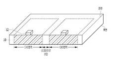
도 1은 본 발명의 실시예들에 따른 커브드 이미지 센서의 구성을 간략히 도시한 도면이다. 구체적으로, 도 1은 본 발명의 실시예들에 따른 커브드 이미지 센서에 적용할 수 있는 이미지 센서의 구성을 간략히 도시한 평면도이다.1 is a diagram schematically illustrating a configuration of a curved image sensor according to embodiments of the present invention. Specifically, FIG. 1 is a plan view schematically illustrating a configuration of an image sensor applicable to a curved image sensor according to embodiments of the present invention.
도 1에 도시된 바와 같이, 실시예들에 따른 이미지 센서는 광전변환소자를 포함하는 복수의 픽셀들이 2차원적으로 배열된 픽셀 어레이(2)를 포함할 수 있다. 픽셀 어레이(2)에 배열된 각 픽셀(1)에는 광전변환소자와 함께 복수의 트랜지스터 및 캐패시터 등으로 구성된 픽셀 회로(미도시)가 접속되어 있다. 또한, 복수의 광전변환소자는 픽셀 회로의 일부를 공유하고 있는 경우도 있다. 또한, 픽셀(1)에서 광전변환소자와 함께 배치되는 픽셀 회로는 광전변환소자가 마련된 표면(또는 광 입사면)과는 반대측의 표면(또는, 광 입사면의 대향면)에 마련될 수 있다.1 , the image sensor according to the embodiments may include a
후술하겠지만, 본 실시예들에 따른 커브드 이미지 센서에서 고정패턴은 픽셀 어레이(2)의 가장자리를 둘러싸는 도넛형태를 가질 수 있고, 본딩패턴은 픽셀 어레이(2)의 센터에 위치할 수 있다.As will be described later, in the curved image sensor according to the present exemplary embodiment, the fixed pattern may have a donut shape surrounding the edge of the
픽셀 어레이(2)의 주변에는 수직구동회로(3), 컬럼신호처리회로(4), 수평구동회로(5) 및 시스템 제어회로(6)를 포함한 주변회로가 배치될 수 있다. 주변회로는 픽셀 어레이(2)와 동일한 기판에 형성될 수 있다(도 2a 및 도 2b 참조). 한편, 주변회로는 픽셀 어레이(2)가 형성된 기판과 상이한 기판에 형성될 수도 있다. 이 경우, 픽셀 어레이(2)와 주변회로를 전기적으로 연결하기 위한 수단 예컨대, 커넥터가 본딩패턴 또는/및 고정패턴에 형성될 수도 있다(도 3a 및 도 3b 참조).Peripheral circuits including a
수직구동회로(3)는 시프트 레지스터에 의해 구성되고, 픽셀 어레이(2)에 배선된 픽셀 구동선(7)를 선택하고, 선택된 픽셀 구동선(7)에 픽셀을 구동하기 위한 펄스신호를 공급하여 픽셀 어레이(2)에 배열된 픽셀을 행(row) 단위로 구동한다. 즉, 수직구동회로(3)는 픽셀 어레이(2)에 배열된 각 픽셀를 행 단위로 순차적으로 수직 방향으로 선택 주사한다. 그리고, 픽셀 구동선(7)에 대해 수직으로 배선된 수직 신호선(8)을 통하여, 각 픽셀에서 수광량에 응하여 생성한 신호 전하에 의거한 픽셀 신호를 컬럼신호처리회로(4)에 공급한다.The
컬럼신호처리회로(4)는 픽셀의 열(column)마다 배치되어 있고, 1행분의 픽셀로부터 출력되는 신호를 픽셀열 마다 노이즈 제거 등의 신호 처리를 행한다. 즉 컬럼신호처리회로(4)는 픽셀 고유의 고정 패턴 노이즈를 제거하기 위한 상관 이중 샘플링(CDS, Correlated Double sampling)이나, 신호 증폭, 아날로그/디지털 변환(ADC, Analog/Digital Conversion) 등의 신호 처리를 행한다.The column
수평구동회로(5)는 시프트 레지스터에 의해 구성되고, 수평 주사 펄스를 순차적으로 출력함에 의해, 컬럼신호처리회로(4)의 각각을 순번대로 선택하고, 컬럼신호처리회로(4)의 각각으로부터 픽셀 신호를 출력시킨다. 출력 회로는 컬럼신호처리회로(4)의 각각으로부터 순차적으로 공급되는 신호에 대해, 신호 처리를 행하여 출력한다. 예를 들면, 버퍼링만 하는 경우도 있고, 다크 레벨 조정, 열(row) 편차 보정, 각종 디지털 신호 처리 등이 행하여지는 경우도 있다.The
시스템 제어회로(6)는 입력 클록과 동작 모드 등을 지령하는 데이터를 수취하고, 이미지 센서 내부 정보 등의 데이터를 출력한다. 즉, 시스템 제어회로(6)에서는 수직 동기 신호, 수평 동기 신호 및 마스터 클록에 의거하여 수직구동회로(3), 컬럼신호처리회로(4) 및 수평구동회로(5) 등의 동작에 기준이 되는 클록 신호나 제어 신호를 생성한다. 그리고, 이들의 신호를 수직구동회로(3), 컬럼신호처리회로(4) 및 수평구동회로(5) 등에 입력한다.
The
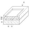
도 2a 및 도 2b는 본 발명의 제1실시예에 따른 커브드 이미지 센서를 도시한 도면이다. 구체적으로, 도 2a는 평면도이고, 도 2b는 도 2a에 도시된 A-A'절취선을 따라 도시한 단면도이다.2A and 2B are diagrams illustrating a curved image sensor according to a first embodiment of the present invention. Specifically, FIG. 2A is a plan view, and FIG. 2B is a cross-sectional view taken along line A-A' shown in FIG. 2A .
도 2a 및 도 2b에 도시된 바와 같이, 제1실시예에 따른 커브드 이미지 센서는 지지기판(120), 지지기판(120) 상에 형성된 본딩패턴(130), 지지기판(120) 상부에서 본딩패턴(130)에 접하고 복수의 광전변환소자(미도시)를 포함하며 만곡된 광 입사면(S1)을 갖는 센서기판(110), 지지기판(120) 상에 형성되어 센서기판(110)의 가장자리를 둘러싸는 고정패턴(140)을 포함할 수 있다. 여기서, 지지기판(120), 센서기판(110) 및 고정패턴(140)에 의해 형성된 공동(air cavity)은 외부로부터 공기의 유입이 차단된 밀폐된 공동(closed air cavity, 150)일 수 있다. 밀폐된 공동(150)은 외부(또는 대기압)보다 낮은 압력을 가질 수 있다.As shown in FIGS. 2A and 2B , the curved image sensor according to the first embodiment includes a
센서기판(110)은 디바이스 웨이퍼(device wafer)일 수 있고, 지지기판(120)은 캐리어 웨이퍼(carrier wafer) 또는 핸들 웨이퍼(handle wafer)일 수 있다. 즉, 센서기판(110)은 복수의 이미지 센서가 형성되는 디바이스 웨이퍼에서 분리된 것일 수 있고, 지지기판(120)은 캐리어 웨이퍼에서 분리된 것일 수 있다. 그리고, 센서기판(110) 및 지지기판(120)은 웨이퍼 씨닝공정에 의해 박막화된 것일 수 있다. 지지기판(120)은 본딩패턴(130) 및 고정패턴(140)과 더불어서 만곡된 광 입사면(S1)을 갖는 센서기판(110)을 지지하는 부재로 작용할 수 있다. 센서기판(110) 및 지지기판(120)은 반도체 기판을 포함할 수 있다. 반도체 기판은 단결정 상태(Single crystal state)일 수 있으며, 실리콘 함유 재료를 포함할 수 있다. 즉, 센서기판(110) 및 지지기판(120)은 단결정의 실리콘 함유 재료를 포함할 수 있다. 일례로, 센서기판(110) 및 지지기판(120)은 벌크 실리콘 기판일 수 있다.The
실시예에 따른 이미지 센서가 후면 수광 타입인 경우에 센서기판(110)에서 만곡된 광 입사면(S1)은 센서기판(110)의 후면(Backside)일 수 있고, 광 입사면(S1)의 반대측 대향면(S2)은 센서기판(110)의 전면(Frontside)일 수 있다. 여기서, 도면에 도시하지는 않았지만, 실시예에 따른 커브드 이미지 센서는 센서기판(110) 전면(Frontside) 즉, 대향면(S2) 상에 형성되어 신호생성회로를 포함하는 층간절연막(미도시)을 더 포함할 수 있다. 층간절연막은 산화막, 질화막 및 산화질화막으로 이루어진 그룹으로부터 선택된 어느 하나의 단일막 또는 둘 이상의 다중막일 수 있다. 층간절연막 내부에 형성된 신호생성회로는 복수의 트랜지스터, 다층의 금속배선, 복수의 캐패시터 및 이들을 상호 연결하는 복수의 콘택플러그를 포함할 수 있다. 여기서, 신호생성회로는 도 1에서 설명한 픽셀 회로 및 주변회로를 포함할 수 있다. 또한, 실시예에 따른 커브드 이미지 센서는 센서기판(110)의 후면(Backside) 즉, 만곡된 광 입사면(S1) 상에서 각각의 광전변환소자에 대응하도록 형성된 컬러필터(미도시) 및 컬러필터 상에 형성된 마이크로렌즈(미도시)를 더 포함할 수 있다.When the image sensor according to the embodiment is a rear light receiving type, the curved light incident surface S1 of the
센서기판(110)에 형성된 광전변환소자는 포토다이오드를 포함할 수 있다. 예컨대, 광전변환소자는 센서기판(110)에 형성되어 수직적으로 중첩되는 하나 이상의 광전변환부들을 포함할 수 있다. 광전변환부들 각각은 P형 불순물영역과 N형 불순물영역을 포함할 수 있다. 아울러, 광전변환소자는 센서기판(110) 상에 형성된 유기광전변환소자를 포함할 수도 있다.The photoelectric conversion element formed on the
지지기판(120) 상의 본딩패턴(130)은 디바이스 웨이퍼를 포함한 센서기판(110)과 캐리어 웨이퍼를 포함한 지지기판(120)을 본딩시키는 접착부재로 작용할 수 있다. 본딩패턴(130)은 센서기판(110)의 대향면(S2)에 접할 수 있다. 본딩패턴(130)은 절연물질을 포함할 수 있다. 구체적으로, 본딩패턴(130)은 산화물, 질화물 및 산화질화물로 이루어진 그룹으로부터 선택된 어느 하나 또는 둘 이상일 수 있다. 일례로, 센서기판(110) 및 지지기판(120)이 실리콘 함유 재료를 포함하는 경우에 본딩패턴(130)은 실리콘산화물 또는 실리콘질화물을 포함할 수 있다.The
또한, 본딩패턴(130)은 센서기판(110)의 만곡된 광 입사면(S1)을 제공하는 역할을 수행할 수 있다. 후술하겠지만, 본딩패턴(130)은 밀폐된 공동(150) 내부의 공기를 팽창시켜 센서기판(110)의 광 입사면(S1)을 만곡시키는 과정에서 광 입사면(S1)이 오목한 형태를 갖도록 센서기판(110)을 잡아주는 역할을 수행할 수 있다. 따라서, 일정한 곡률을 갖는 만곡된 광 입사면(S1)을 제공하기 위해 본딩패턴(130)은 센서기판(110)의 센터에 접할 수 있다. 구체적으로, 본딩패턴(130)은 센서기판(110)에 형성된 픽셀 어레이의 센터에 접할 수 있다. 아울러, 본딩패턴(130)의 평면은 사각형 이상의 다각형 또는 원형일 수 있고, 본딩패턴(130)의 가로세로비는 센서기판(110)의 가로세로비와 동일할 수 있다.In addition, the
지지기판(120)과 센서기판(110) 사이에서 충분한 접착력을 유지하기 위해 본딩패턴(130)의 면적 또는 본딩패턴(130)과 센서기판(110)이 접하는 면적은 센서기판(110)의 면적 대비 10% 내지 20% 범위일 수 있다. 참고로, 본딩패턴(130)의 면적이 10% 미만인 경우에는 충분한 접착력을 제공하기 어렵고, 20%를 초과하는 경우에는 만곡된 광 입사면(S1)의 곡률이 일정하지 않아 이미지 센서의 특성이 열화될 수 있다.In order to maintain sufficient adhesive force between the
고정패턴(140)은 본딩패턴(130)과 더불어서 지지기판(120)과 센서기판(110) 사이를 결합시키는 역할을 수행한다. 아울러, 고정패턴(140)은 지지기판(120) 및 센서기판(110)과 더불어서 밀폐된 공동(150)을 제공하는 역할을 수행한다. 이를 위해, 고정패턴(140)은 도넛형태를 가질 수 있다. 고정패턴(140)은 열경화성을 갖는 물질을 포함할 수 있다.The fixing
또한, 고정패턴(140)은 센서기판(110)의 광 입사면(S1)이 만곡된 상태를 유지하도록 고정해주는 역할을 수행한다. 이를 위해, 고정패턴(140)은 센서기판(110)의 가장자리를 둘러싸는 형태를 가질 수 있고, 본딩패턴(130)보다 큰 높이(또는 두께)를 가질 수 있다. 구체적으로, 고정패턴(140)은 적어도 센서기판(110)의 가장자리 측벽에 접하는 형태를 가질 수 있다. 보다 구체적으로, 고정패턴(140)은 센서기판(110) 가장자리의 전면, 측면 및 후면에 모두 접하는 형태를 가질 수 있다. 즉, 센서기판(110)의 가장자리가 고정패턴(140)에 박힌 형태를 가질 수 있다. 여기서, 고정패턴(140)과 센서기판(110) 사이의 접촉면적 증가를 통한 접착력 증대를 위해 센서기판(110)은 경사진 측벽을 가질 수 있다.In addition, the fixing
상술한 제1실시예에 따른 커브드 이미지 센서는 본딩패턴(130) 및 고정패턴(140)을 이용하여 센서기판(110)의 만곡된 광 입사면(S1)을 제공함으로써, 생산 효율을 현저하게 증진시킬 수 있다. 또한, 커브드 이미지 센서를 포함한 패키지의 소형화가 가능하다. 이는, 후술하는 커브드 이미지 센서의 제조방법(도 4a 내지 도 4f)을 통해 보다 명확해질 것이다.
The curved image sensor according to the above-described first embodiment provides a curved light incident surface S1 of the
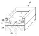
도 3a 및 도 3b는 본 발명의 제2실시예에 따른 커브드 이미지 센서를 도시한 도면이다. 구체적으로, 도 3a는 평면도이고, 도 3b는 도 3a에 도시된 A-A'절취선을 따라 도시한 단면도이다. 여기서는, 제1실시예와 동일한 구성에 대하여 동일한 도면부호를 사용하며, 자세한 설명은 생략하기로 한다.3A and 3B are diagrams illustrating a curved image sensor according to a second embodiment of the present invention. Specifically, FIG. 3A is a plan view, and FIG. 3B is a cross-sectional view taken along line A-A' shown in FIG. 3A. Here, the same reference numerals are used for the same components as those of the first embodiment, and detailed descriptions thereof will be omitted.
도 3a 및 도 3b에 도시된 바와 같이, 제2실시예에 따른 커브드 이미지 센서는 지지기판(120), 지지기판(120) 상에 형성된 로직회로층(210), 로직회로층(210) 상에 형성된 본딩패턴(130), 지지기판(120) 상부에서 본딩패턴(130)에 접하고 복수의 광전변환소자(미도시)를 포함하며 만곡된 광 입사면(S1)을 갖는 센서기판(110), 로직회로층(210) 상에 형성되어 센서기판(110)의 가장자리를 둘러싸는 고정패턴(140) 및 고정패턴(140)을 관통하여 센서기판(110)과 로직회로층(210)을 전기적으로 연결하는 복수의 커넥터(220)를 포함할 수 있다, 여기서, 지지기판(120), 센서기판(110) 및 고정패턴(140)에 의해 형성된 공동은 외부로부터 공기의 유입이 차단된 밀폐된 공동(150)일 수 있다. 밀폐된 공동(150)은 외부(또는 대기압)보다 낮은 압력을 가질 수 있다.3A and 3B , the curved image sensor according to the second embodiment includes a
실시예에 따른 이미지 센서가 후면 수광 타입인 경우에 센서기판(110)에서 만곡된 광 입사면(S1)은 센서기판(110)의 후면(Backside)일 수 있고, 광 입사면(S1)의 반대측 대향면(S2)은 센서기판(110)의 전면(Frontside)일 수 있다. 여기서, 도면에 도시하지는 않았지만, 실시예에 따른 커브드 이미지 센서는 센서기판(110) 전면(Frontside) 즉, 대향면(S2) 상에 형성되어 신호생성회로를 포함하는 층간절연막(미도시)을 더 포함할 수 있다. 층간절연막은 산화막, 질화막 및 산화질화막으로 이루어진 그룹으로부터 선택된 어느 하나의 단일막 또는 둘 이상의 다중막일 수 있다. 층간절연막 내부에 형성된 신호생성회로는 복수의 트랜지스터, 다층의 금속배선, 복수의 캐패시터 및 이들을 상호 연결하는 복수의 콘택플러그를 포함할 수 있다. 여기서, 신호생성회로는 도 1에서 설명한 픽셀 회로 및 주변회로를 포함할 수 있다. 또한, 실시예에 따른 커브드 이미지 센서는 센서기판(110)의 후면(Backside) 즉, 만곡된 광 입사면(S1) 상에서 각각의 광전변환소자에 대응하도록 형성된 컬러필터(미도시) 및 컬러필터 상에 형성된 마이크로렌즈(미도시)를 더 포함할 수 있다.When the image sensor according to the embodiment is a rear light receiving type, the curved light incident surface S1 of the
지지기판(120) 상에 형성된 로직회로층(210)은 도 1에서 설명한 주변회로를 포함하거나, 또는 ISP(Image Signal Processing)를 포함한 이미지 프로세싱 회로를 포함할 수 있다. 로직회로층(210)은 상술한 신호생성회로와 마찬가지로, 복수의 트랜지스터, 다층의 금속배선, 이들을 상호 연결하는 복수의 콘택플러그 및 커넥터(220)와 접속되는 패드를 포함할 수 있다. 아울러, 막내 이들이 형성된 층간절연막을 포함할 수 있다.The
한편, 제2실시예에서는 복수의 커넥터(220)가 고정패턴(140)에 형성된 경우를 예시하였으나, 복수의 커넥터(220)는 고정패턴(140)과 더불어서 본딩패턴(130)에도 형성될 수 있다.Meanwhile, in the second embodiment, the case where the plurality of
상술한 제2실시예에 따른 커브드 이미지 센서는 본딩패턴(130) 및 고정패턴(140)을 이용하여 센서기판(110)의 만곡된 광 입사면(S1)을 제공함으로써, 생산 효율을 현저하게 증진시킬 수 있다. 또한, 커브드 이미지 센서를 포함한 패키지의 소형화가 가능하다. 이는, 후술하는 커브드 이미지 센서의 제조방법(도 4a 내지 도 4f)을 통해 보다 명확해질 것이다.The curved image sensor according to the above-described second embodiment provides the curved light incident surface S1 of the
또한, 로직회로층(210) 및 커넥터(220)를 구비함으로써, 커브드 이미지 센서의 집적도를 향상시켜 초소형화가 가능하고, 동작속도를 향상시킬 수 있다.
In addition, by providing the
도 4a 내지 도 4f는 본 발명의 실시예에 따른 커브드 이미지 센서의 제조방법을 도시한 사시도이다. 여기서는, 제1실시예에 따른 커브드 이미지 센서를 제조하는 방법에 대한 일례를 설명하기로 한다. 도 4a 내지 도 4f는 도 2a에 도시된 A-A'절취선에 따른 단면이 드러나도록 도시한 사시도이다.4A to 4F are perspective views illustrating a method of manufacturing a curved image sensor according to an exemplary embodiment of the present invention. Here, an example of a method of manufacturing the curved image sensor according to the first embodiment will be described. 4A to 4F are perspective views showing a cross-section taken along line A-A' shown in FIG. 2A to be exposed.
도 4a에 도시된 바와 같이, 복수의 다이영역 및 스크라이브 레인(Scribe Lane)을 갖는 디바이스 웨이퍼(10)를 준비한다. 디바이스 웨이퍼(10)는 단결정 상태일 수 있으며, 실리콘 함유 재료를 포함할 수 있다. 일례로, 디바이스 웨이퍼(10)는 벌크 실리콘 웨이퍼일 수 있다.As shown in FIG. 4A , a
다음으로, 각각의 다이영역에 복수의 광전변환소자(미도시)를 포함한 이미지 센서(미도시)를 형성한다. 예컨대, 도면에 도시하지는 않았지만, 디바이스 웨이퍼(10)에 복수의 광전변환소자를 형성하고, 디바이스 웨이퍼(10) 전면 상에 신호생성회로를 포함하는 층간절연막을 순차적으로 형성할 수 있다.Next, an image sensor (not shown) including a plurality of photoelectric conversion elements (not shown) is formed in each die region. For example, although not shown in the drawings, a plurality of photoelectric conversion elements may be formed on the
다음으로, 각각의 다이영역 상에 본딩패턴(12)을 형성한다. 본딩패턴(12)은 후속 웨이퍼 본딩시 두 웨이퍼 사이의 접착력을 향상시키기 위한 것이다. 아울러, 본딩패턴(12)은 두 웨이퍼 사이에 공동을 형성하기 위한 것이다. 아울러, 본딩패턴(12)은 만곡된 광 입사면을 형성하기 위한 것이다. 본딩패턴(12)은 절연물질을 포함할 수 있다. 구체적으로, 본딩패턴(12)은 산화물, 질화물 및 산화질화물로 이루어진 그룹으로부터 선택된 어느 하나 또는 둘 이상을 포함할 수 있다. 일례로, 본딩패턴(12)은 실리콘질화물로 형성할 수 있다.Next, a
본딩패턴(12)은 디바이스 웨이퍼(10) 상에 절연막을 형성한 다음, 절연막을 선택적으로 식각하여 형성할 수 있다. 본딩패턴(12)은 디바이스 웨이퍼(10)의 전면(Frontside) 상에 형성할 수 있으며, 다이영역의 센터에 위치하도록 형성할 수 있다. 구체적으로, 본딩패턴(12)은 다이영역에서 복수의 픽셀들이 2차원 배열되는 픽셀 어레이의 센터에 위치하도록 형성할 수 있다. 본딩패턴(12)의 면적 또는 본딩패턴(12)과 다이영역이 접하는 면적은 다이영역의 면적 대비 10% 내지 20%의 면적을 갖도록 형성할 수 있다. 본딩패턴(12)의 평면은 사각형 이상의 다각형 또는 원형일 수 있다. 본딩패턴(12)의 가로세로비(aspect ratio)는 다이영역의 가로세로비와 동일할 수 있다. 이는, 후속 공정에서 일정한 곡률을 갖도록 만곡된 광 입사면을 형성하기 위함이다.The
도 4b에 도시된 바와 같이, 디바이스 웨이퍼(10) 상에 본딩패턴(12) 사이를 매립하는 희생막(14)을 형성한다. 희생막(14)은 본딩패턴(12)의 상부면과 평탄한 상부면을 갖도록 형성할 수 있다. 따라서, 희생막(14)은 디바이스 웨이퍼(10) 상에 본딩패턴(12) 사이를 매립하도록 충분한 두께를 갖는 물질막을 형성한 후, 본딩패턴(12)의 표면이 노출될때까지 물질막에 대한 평탄화공정 예컨대, 화학적기계적연마(CMP)를 진행하여 형성할 수 있다. 희생막(14)은 잔류물 없이 제거가 용이하고, 본딩패턴(12)과 식각선택비를 갖는 물질로 형성할 수 있다. 예컨대, 본딩패턴(12)을 실리콘질화물로 형성한 경우에 희생막(14)은 탄소함유물 또는 실리콘산화물로 형성할 수 있다.As shown in FIG. 4B , a
다음으로, 캐리어 웨이퍼(30)를 준비한다. 캐리어 웨이퍼(30)는 단결정 상태일 수 있으며, 실리콘 함유 재료를 포함할 수 있다. 일례로, 캐리어 웨이퍼(30)는 벌크 실리콘 웨이퍼일 수 있다.Next, the
다음으로, 본딩패턴(12) 및 희생막(14)이 형성된 디바이스 웨이퍼(10)에 캐리어 웨이퍼(30)를 본딩한다. 이때, 본딩패턴(12)이 디바이스 웨이퍼(10) 및 캐리어 웨이퍼(30) 양측에 모두 접하도록 웨이퍼 본딩공정(wafer bonding process)을 진행한다. 웨이퍼 본딩공정은 공지된 다양한 방법을 사용하여 진행할 수 있다.Next, the
도 4c에 도시된 바와 같이, 디바이스 웨이퍼(10) 후면(Backside)에 대한 씨닝공정(thinning process)을 진행하여 디바이스 웨이퍼(10)의 두께를 감소시킨다. 이어서, 도면에 도시하지는 않았지만, 디바이스 웨이퍼(10) 후면(Backside) 상에 각각의 광전변환소자에 대응하도록 컬러필터(미도시) 및 마이크로렌즈(미도시)를 순차적으로 형성한다. 이하, 씨닝공정을 진행하여 박막화된 디바이스 웨이퍼(10)의 도면부호를 '10A'로 변경하여 표기하기로 한다.As shown in FIG. 4C , a thinning process is performed on the backside of the
다음으로, 스크라이브 레인에 대응하는 디바이스 웨이퍼(10A)를 선택적으로 식각하여 각각의 다이영역을 분리하는 트렌치(16)를 형성한다. 트렌치(16)는 경사진 측벽을 갖도록 형성할 수 있다. 따라서, 각각의 다이영역도 경사진 측벽을 가질 수 있다. 구체적으로, 트렌치(16)는 하부영역에서 상부영역으로 갈수록 선폭이 증가하도록 경사진 측벽을 가질 수 있다. 이를 위해, 트렌치(16)를 형성하기 위한 식각공정은 건식식각으로 진행할 수 있다. 트렌치(16)를 형성하기 위한 식각공정은 희생막(14)이 노출되거나, 또는 캐리어 웨이퍼(30)가 노출될때까지 진행할 수 있다.Next, the
다음으로, 희생막(14)을 제거한다. 이때, 희생막(14)을 제거함에 따라 디바이스 웨이퍼(10A)의 다이영역과 캐리어 웨이퍼(30) 사이에 공동(18)을 형성할 수 있다. 희생막(14)은 희생막(14)으로 사용된 물질에 따라 다양한 방법으로 제거할 수 있다. 예컨대, 희생막(14)을 탄소함유물로 형성한 경우에는 애싱공정을 통해 제거할 수 있고, 실리콘산화물로 형성한 경우에는 불산(HF)계열의 식각제(etchant)를 사용하여 제거할 수 있다.Next, the
한편, 실시예에 따른 커브드 이미지 센서 제조방법의 변형예로서, 희생막(14)을 형성하지 않고 웨이퍼 본딩공정을 진행할 수도 있다. 이 경우, 별도의 희생막(14) 제거공정을 필요로하지 않으며, 웨이퍼 본딩공정이 완료된 시점에서 디바이스 웨이퍼(10)와 캐리어 웨이퍼(30) 사이에 공동(18)이 형성된다.Meanwhile, as a modification of the method for manufacturing the curved image sensor according to the embodiment, the wafer bonding process may be performed without forming the
도 4d에 도시된 바와 같이, 트렌치(16)를 매립하는 고정막(20)을 형성한다. 고정막(20)을 형성함에 따라 디바이스 웨이퍼(10A)와 캐리어 웨이퍼(30) 사이의 공동(18)을 외부로부터 공기의 유입이 차단된 밀폐된 공동(22)으로 전환시킬 수 있다.As shown in FIG. 4D , a pinned film 20 filling the
트렌치(16)를 매립하는 고정막(20)은 적어도 다이영역의 측벽에 접하는 형태를 가질 수 있다. 스크라이브 레인에 대응하는 영역에 선택적으로 고정막(20)을 형성함과 동시에 고정막(20)이 밀폐된 공동(22)을 매립하는 것을 방지하기 위해 고정막(20)은 점성을 갖는 폴리머로 형성할 수 있다. 이때, 폴리머는 열경화성을 가질 수 있다. 고정막(20)을 점성을 갖는 폴리머로 형성함에 따라 고정막(20)은 일부가 트렌치(16) 저면 아래로 확장되어 캐리어 웨이퍼(30)에 접하고, 다이영역 가장자리의 전면(Frontside)에 접하는 형태를 가질 수 있다. 이때, 폴리머의 점성 및 다이영역의 경사진 측벽으로 인해 고정막(20)이 본딩패턴(12) 측으로 확장되는 것을 방지할 수 있다. 즉, 고정막(20)이 밀폐된 공동(22)을 매립하는 것을 방지할 수 있다. 아울러, 고정막(20)은 일부가 트렌치(16) 위로 돌출되어 다이영역의 가장자리 후면(Backside)에 접하는 형태를 가질 수 있다. 결과적으로, 고정막(20)은 캐리어 웨이퍼(30) 상에서 디바이스 웨이퍼(10A) 다이영역의 가장자리를 둘러싸되, 가장자리의 전면, 측면 및 후면에 접하는 형태를 가질 수 있다. 즉, 다이영역의 가장자리가 고정막(20)에 박힌 형태를 가질 수 있다.The pinned layer 20 filling the
다음으로, 고정막(20)에 대한 어닐링 진행한다. 이는, 후속 쏘잉공정을 진행할 수 있는 수준의 기계적강도를 확보하기 위한 것으로, 열경화성을 갖는 고정막(20)을 완전히 경화시키기 위한 것은 아니다.Next, annealing is performed on the fixed film 20 . This is to secure a level of mechanical strength that can proceed with the subsequent sawing process, and is not intended to completely cure the fixing film 20 having thermosetting properties.
도 4e에 도시된 바와 같이, 스크라이브 레인을 따라 각각의 다이(40)를 분리시키는 쏘잉공정(sawing process)을 진행한다. 쏘잉공정은 고정막(20)과 캐리어 웨이퍼(30)를 대상으로 진행할 수 있다. 이하, 쏘잉공정으로 분리된 캐리어 웨이퍼(30) 및 디바이스 웨이퍼(10A)는 각각 '지지기판(30A)' 및 '센서기판(10B)'으로 변경하여 표기하기로 한다. 그리고, 쏘잉공정으로 분리된 고정막(20)의 도면부호를 '20A'로 변경하여 표기하기로 한다.As shown in FIG. 4E, a sawing process of separating each die 40 along the scribe lane is performed. The sawing process may be performed on the fixed film 20 and the
쏘잉공정으로 분리된 각각의 다이(40)는 지지기판(30A), 지지기판(30A) 상의 본딩패턴(12), 지지기판(30A) 상부에서 본딩패턴(12)에 접하는 센서기판(10B), 지지기판(30A) 상에서 센서기판(10B)의 가장자리를 둘러싸는 고정막(20A)을 포함할 수 있다. 쏘잉공정이 완료된 시점에서 각각의 다이(40)에서 센서기판(10B)은 평탄한 광 입사면을 가질 수 있다. 그리고, 지지기판(30A), 센서기판(10B) 및 고정막(20A)에 의해 밀폐된 공동(22)의 내부는 외부와 동일한 압력을 가질 수 있다.Each die 40 separated by the sawing process is a
한편, 쏘잉공정을 진행하기 이전에 캐리어 웨이퍼(30)에 대한 씨닝공정을 진행할 수 있다.On the other hand, it is possible to proceed with the thinning process of the
도 4f에 도시된 바와 같이, 챔버에 복수의 다이(40)를 로딩한 후 어닐링을 진행하여 만곡된 표면을 갖는 다이(40)를 형성함과 동시에 만곡된 표면을 고정 및 유지하는 고정패턴(24)을 형성한다. 여기서, 만곡된 표면은 센서기판(10B)의 광 입사면일 수 있다. 이하, 만곡된 광 입사면을 갖는 센서기판(10B)의 도면부호를 '10C'로 변경하고, 만곡된 표면을 갖는 다이(40)에서의 밀폐된 공동(22)의 도면부호를 '22A'로 변경하여 표기한다.As shown in FIG. 4F, after loading a plurality of dies 40 into the chamber, annealing is performed to form a die 40 having a curved surface, and a fixing
어닐링을 진행함에 따라 밀폐된 공동(22A) 내부의 공기가 팽창한다. 본딩패턴(12)에 의해 센서기판(10C)의 센터가 지지기판(30A)에 고정된 상태에서 밀폐된 공동(22A) 내부의 공기가 팽창하면, 센서기판(10C)의 가장자리가 상승하면서 광 입사면을 만곡시킬 수 있다. 이때, 어닐링은 열경화성을 갖는 고정막(20A)의 형태를 변형시킬 수 있는 온도 범위에서 진행할 수 있다. 따라서, 센서기판(10C)의 가장자리가 상승함에 따라 센서기판(10C)의 가장자리에 접하는 고정막(20A)의 형태 특히, 높이가 변화하면서 고정패턴(24)을 형성할 수 있다. 구체적으로, 고정막(20A) 대비 고정패턴(24)의 높이가 더 클 수 있다.As the annealing proceeds, the air inside the
이후, 어닐링이 완료된 시점에서 열경화성을 갖는 고정패턴(24)은 외부 온도 변화에 상관없이 그 형태를 유지할 수 있다. 이를 통해, 만곡된 광 입사면을 유지할 수 있다. 아울러, 밀폐된 공동(22A)은 내부 체적이 증가함에 따라 밀폐된 공동(24) 내부는 외부보다 낮은 압력을 가질 수 있으며, 이를 통해 만곡된 광 입사면을 보다 효과적으로 유지할 수 있다.Thereafter, when the annealing is completed, the thermosetting
상술한 공정을 통해 실시예에 따른 커브드 이미지 센서를 완성할 수 있다. 이후, 공지된 패키징 공정을 진행하여 커브드 이미지 센서를 구비한 장치 또는 모듈을 완성할 수 있다.Through the above-described process, the curved image sensor according to the embodiment may be completed. Thereafter, a device or module having a curved image sensor may be completed by performing a known packaging process.
이처럼, 실시예에 따른 커브드 이미지 센서 제조방법은 패키징 공정 이전에 웨이퍼 레벨에서 모든 공정이 진행됨에 따라 생산 효율을 현저하게 증진시킬 수 있다. 아울러, 커브드 이미지 센서를 포함한 패키지의 크기(특히, 높이/두께)를 효과적으로 감소시킬 수 있다.
As such, the manufacturing method of the curved image sensor according to the embodiment can significantly improve production efficiency as all processes are performed at the wafer level before the packaging process. In addition, it is possible to effectively reduce the size (particularly, height/thickness) of a package including the curved image sensor.
상술한 실시예에 따른 커브드 이미지 센서는 다양한 전자장치 또는 시스템에 이용될 수 있다. 이하에서는, 도 5를 참조하여 카메라에 본 발명의 실시예에 따른 커브드 이미지 센서를 적용한 경우를 예시하여 설명하기로 한다.The curved image sensor according to the above-described embodiment may be used in various electronic devices or systems. Hereinafter, a case in which a curved image sensor according to an embodiment of the present invention is applied to a camera will be described with reference to FIG. 5 .
도 5는 본 발명의 실시예에 따른 커브드 이미지 센서를 구비한 전자장치를 간략히 도시한 도면이다.5 is a diagram schematically illustrating an electronic device having a curved image sensor according to an embodiment of the present invention.
도 5를 참조하여, 실시예에 따른 커브드 이미지 센서를 구비한 전자장치는 정지영상 또는 동영상을 촬영할 수 있는 카메라일 수 있다. 전자장치는 커브드 이미지 센서(300), 광학 시스템(또는, 광학 렌즈)(310), 셔터 유닛(311), 커브드 이미지 센서(300) 및 셔터 유닛(311)을 제어/구동하는 구동부(313) 및 신호 처리부(312)를 포함할 수 있다.Referring to FIG. 5 , an electronic device having a curved image sensor according to an embodiment may be a camera capable of capturing a still image or a moving image. The electronic device includes a
광학 시스템(310)은 피사체로부터의 이미지 광(입사광)을 커브드 이미지 센서(300)의 픽셀 어레이(도 1의 도면부호 '2' 참조)로 안내한다. 광학 시스템(310)은 복수의 광학 렌즈로 구성될 수 있다. 셔터 유닛(311)은 커브드 이미지 센서(300)에 대한 광 조사 기간 및 차폐 기간을 제어한다. 구동부(313)는 커브드 이미지 센서(300)의 전송 동작과 셔터 유닛(311)의 셔터 동작을 제어한다. 신호 처리부(312)는 커브드 이미지 센서(300)로부터 출력된 신호에 관해 다양한 종류의 신호 처리를 수행한다. 신호 처리 후의 이미지 신호(Dout)는 메모리 등의 저장 매체에 저장되거나, 모니터 등에 출력된다.
The
본 발명의 기술 사상은 상기 바람직한 실시예에 따라 구체적으로 기술되었으나, 상기 실시예는 그 설명을 위한 것이며, 그 제한을 위한 것이 아님을 주의하여야 한다. 또한, 본 발명의 기술분야의 통상의 전문가라면 본 발명의 기술사상의 범위내의 다양한 실시예가 가능함을 이해할 수 있을 것이다.
Although the technical spirit of the present invention has been specifically described according to the above preferred embodiments, it should be noted that the above embodiments are for explanation only and not for limitation. In addition, those skilled in the art will understand that various embodiments within the scope of the technical spirit of the present invention are possible.
110 : 센서기판120 : 지지기판
130 : 본딩패턴140 : 고정패턴
150 : 밀폐된 공동110: sensor substrate 120: support substrate
130: bonding pattern 140: fixed pattern
150: closed cavity
Claims (26)
Translated fromKorean상기 지지기판 상에 형성된 본딩패턴;
상기 지지기판 상부에서 상기 본딩패턴에 접하고 만곡된 광 입사면을 갖는 센서기판; 및
상기 지지기판 상에 형성되어 센서기판의 가장자리를 둘러싸는 고정패턴
을 포함하되,
상기 본딩 패턴은 상기 센서기판과 상기 지지기판을 본딩하는 접착부재로서 상기 센싱기판의 센터에 접하며,
상기 센싱기판의 측벽은 상기 고정패턴에 의해 전체적으로 둘러쌓여서 고정되고,
상기 고정패턴은 상기 지지기판과는 서로 다른 물질을 가지되,
상기 고정패턴은 적어도 상기 센서기판의 가장자리 측벽에 접하는 커브드 이미지 센서.
support substrate;
a bonding pattern formed on the support substrate;
a sensor substrate contacting the bonding pattern on the support substrate and having a curved light incident surface; and
A fixed pattern formed on the support substrate and surrounding the edge of the sensor substrate
including,
The bonding pattern is an adhesive member for bonding the sensor substrate and the support substrate and is in contact with the center of the sensing substrate,
The side wall of the sensing substrate is completely surrounded and fixed by the fixing pattern,
The fixing pattern has a material different from that of the support substrate,
The fixed pattern is a curved image sensor in contact with at least an edge sidewall of the sensor substrate.
상기 센서기판, 상기 지지기판 및 상기 고정패턴에 의한 밀폐된 공동을 더 포함하고, 상기 밀폐된 공동은 외부보다 낮은 압력을 갖는 커브드 이미지 센서.
According to claim 1,
The curved image sensor further includes a cavity closed by the sensor substrate, the support substrate, and the fixed pattern, wherein the closed cavity has a lower pressure than the outside.
상기 센서기판은 디바이스 웨이퍼를 포함하고, 상기 지지기판은 캐리어 웨이퍼를 포함하는 커브드 이미지 센서.
According to claim 1,
The sensor substrate includes a device wafer, and the support substrate includes a carrier wafer.
상기 본딩패턴은 상기 센서기판의 면적 대비 10% 내지 20% 범위 면적을 갖는 커브드 이미지 센서.
According to claim 1,
The bonding pattern is a curved image sensor having an area in the range of 10% to 20% of the area of the sensor substrate.
상기 본딩패턴의 가로세로비는 상기 센서기판의 가로세로비와 동일한 커브드 이미지 센서.
According to claim 1,
The aspect ratio of the bonding pattern is the same as the aspect ratio of the sensor substrate.
상기 센서기판은 경사진 측벽을 갖는 커브드 이미지 센서.
According to claim 1,
The sensor substrate is a curved image sensor having an inclined sidewall.
상기 고정패턴은 도넛형태를 갖는 커브드 이미지 센서.
According to claim 1,
The fixed pattern is a curved image sensor having a donut shape.
상기 고정패턴은 열경화성을 갖는 물질을 포함하는 커브드 이미지 센서.
According to claim 1,
The fixed pattern is a curved image sensor including a material having a thermosetting property.
상기 지지기판 상에 형성된 로직회로층;
상기 로직회로층 상에 형성된 본딩패턴;
상기 지지기판 상부에서 상기 본딩패턴에 접하고 만곡된 광 입사면을 갖는 센서기판;
상기 로직회로층 상에 형성되어 상기 센서기판의 가장자리를 둘러싸는 고정패턴; 및
상기 고정패턴을 관통하여 상기 센서기판과 상기 로직회로층을 전기적으로 연결하는 복수의 커넥터
를 포함하되,
상기 본딩 패턴은 상기 센서기판과 상기 지지기판을 본딩하는 접착부재로서 상기 센싱기판의 센터에 접하며,
상기 센싱기판의 측벽은 상기 고정패턴에 의해 전체적으로 둘러쌓여서 고정되고,
상기 고정패턴은 상기 지지기판과는 서로 다른 물질을 가지되,
상기 고정패턴은 적어도 상기 센서기판의 가장자리 측벽에 접하는 커브드 이미지 센서.
support substrate;
a logic circuit layer formed on the support substrate;
a bonding pattern formed on the logic circuit layer;
a sensor substrate contacting the bonding pattern on the support substrate and having a curved light incident surface;
a fixing pattern formed on the logic circuit layer and surrounding an edge of the sensor substrate; and
A plurality of connectors passing through the fixing pattern and electrically connecting the sensor substrate and the logic circuit layer
including,
The bonding pattern is an adhesive member for bonding the sensor substrate and the support substrate and is in contact with the center of the sensing substrate,
The sidewall of the sensing substrate is completely surrounded and fixed by the fixing pattern,
The fixing pattern has a material different from that of the support substrate,
The fixed pattern is at least a curved image sensor in contact with an edge sidewall of the sensor substrate.
상기 로직회로층을 포함한 지지기판, 상기 센서기판 및 상기 고정패턴에 의한 밀폐된 공동을 더 포함하고, 상기 밀폐된 공동은 외부보다 낮은 압력을 갖는 커브드 이미지 센서.
12. The method of claim 11,
The curved image sensor further comprising: a support substrate including the logic circuit layer;
상기 센서기판은 디바이스 웨이퍼를 포함하고, 상기 지지기판은 캐리어 웨이퍼를 포함하는 커브드 이미지 센서.
12. The method of claim 11,
The sensor substrate includes a device wafer, and the support substrate includes a carrier wafer.
상기 고정패턴은 열경화성을 갖는 물질을 포함하는 커브드 이미지 센서.
12. The method of claim 11,
The fixed pattern is a curved image sensor including a material having a thermosetting property.
각각의 상기 다이영역 상에 본딩패턴을 형성하는 단계;
상기 본딩패턴에 접하도록 상기 디바이스 웨이퍼에 캐리어 웨이퍼를 본딩시키는 단계;
상기 스크라이브 레인에 대응하는 상기 디바이스 웨이퍼를 선택적으로 식각하여 각각의 상기 다이영역을 분리시키는 트렌치를 형성하는 단계;
상기 트렌치를 매립하고 일부가 상기 트렌치 아래로 확장되어 상기 캐리어 웨이퍼에 접하는 고정막을 형성하여 상기 캐리어 웨이퍼와 각각의 상기 다이영역 사이에 밀폐된 공동을 형성하는 단계;
상기 스크라이브 레인을 따라 각각의 상기 다이영역을 분리하는 쏘잉공정을 진행하여 복수의 다이를 형성하는 단계; 및
상기 다이의 표면을 만곡시킴과 동시에 만곡된 표면을 유지하는 고정패턴을 형성하는 단계
를 포함하는 커브드 이미지 센서 제조방법.
preparing a device wafer having a plurality of die regions and scribe lanes;
forming a bonding pattern on each of the die regions;
bonding a carrier wafer to the device wafer so as to be in contact with the bonding pattern;
selectively etching the device wafer corresponding to the scribe lane to form a trench separating each of the die regions;
forming a sealed cavity between the carrier wafer and each of the die regions by filling the trench and forming a fixed film partially extending under the trench to contact the carrier wafer;
forming a plurality of dies by performing a sawing process of separating each die region along the scribe lane; and
Forming a fixing pattern that curves the surface of the die and maintains the curved surface at the same time
A method of manufacturing a curved image sensor comprising a.
상기 본딩패턴을 상기 다이영역의 센터에 위치하도록 형성하는 커브드 이미지 센서 제조방법.
18. The method of claim 17,
A method of manufacturing a curved image sensor for forming the bonding pattern to be positioned at a center of the die region.
상기 본딩패턴을 상기 다이영역의 면적 대비 10% 내지 20% 범위의 면적을 갖도록 형성하는 커브드 이미지 센서 제조방법.
18. The method of claim 17,
A method of manufacturing a curved image sensor for forming the bonding pattern to have an area ranging from 10% to 20% of the area of the die region.
상기 본딩패턴의 가로세로비는 상기 다이영역의 가로세로비와 동일하도록 형성하는 커브드 이미지 센서 제조방법.
18. The method of claim 17,
A method for manufacturing a curved image sensor in which an aspect ratio of the bonding pattern is formed to be the same as an aspect ratio of the die region.
상기 디바이스 웨이퍼에 상기 캐리어 웨이퍼를 본딩시키기 이전에,
상기 디바이스 웨이퍼 상에 상기 본딩패턴과 평탄한 표면을 갖는 희생막을 형성하는 단계를 더 포함하고,
상기 고정막을 형성하기 이전에,
상기 희생막을 제거하는 단계를 더 포함하는 커브드 이미지 센서 제조방법.
18. The method of claim 17,
Prior to bonding the carrier wafer to the device wafer,
Further comprising the step of forming a sacrificial film having a flat surface and the bonding pattern on the device wafer,
Before forming the fixing film,
The method of manufacturing a curved image sensor further comprising removing the sacrificial layer.
상기 트렌치는 경사진 측벽을 갖도록 형성하는 커브드 이미지 센서 제조방법.
18. The method of claim 17,
The method of manufacturing a curved image sensor in which the trench is formed to have an inclined sidewall.
상기 다이의 표면을 만곡시킴과 동시에 만곡된 표면을 유지하는 고정패턴을 형성하는 단계는, 상기 밀폐된 공동 내 공기를 팽창시킴과 동시에 상기 고정막의 형태를 변형시킬 수 있는 온도 범위에서 어닐링을 진행하는 커브드 이미지 센서 제조방법.
18. The method of claim 17,
In the step of forming a fixed pattern for maintaining the curved surface while curving the surface of the die, annealing is performed in a temperature range that can change the shape of the fixed film while expanding the air in the closed cavity. A method for manufacturing a curved image sensor.
상기 고정막은 점성을 갖는 폴리머를 포함하고,
상기 폴리머는 열경화성을 갖는 커브드 이미지 센서 제조방법.
24. The method of claim 23,
The fixing film comprises a polymer having viscosity,
The polymer is a method of manufacturing a curved image sensor having thermosetting.
상기 광학 시스템으로부터 광을 수신하는 커브드 이미지 센서; 및
상기 커브드 이미지 센서로부터 출력된 신호에 대해 신호 처리 동작을 수행하는 신호 처리부를 포함하고,
상기 커브드 이미지 센서는,
지지기판;
상기 지지기판 상에 형성된 본딩패턴;
상기 지지기판 상부에서 상기 본딩패턴에 접하고 만곡된 광 입사면을 갖는 센서기판; 및
상기 지지기판 상에 형성되어 센서기판의 가장자리를 둘러싸는 고정패턴
을 포함하되,
상기 본딩 패턴은 상기 센서기판과 상기 지지기판을 본딩하는 접착부재로서 상기 센싱기판의 센터에 접하며,
상기 센싱기판의 측벽은 상기 고정패턴에 의해 전체적으로 둘러쌓여서 고정되고,
상기 고정패턴은 상기 지지기판과는 서로 다른 물질을 가지되,
상기 고정패턴은 적어도 상기 센서기판의 가장자리 측벽에 접하는 전자장치.
optical system;
a curved image sensor for receiving light from the optical system; and
and a signal processing unit that performs a signal processing operation on the signal output from the curved image sensor,
The curved image sensor,
support substrate;
a bonding pattern formed on the support substrate;
a sensor substrate contacting the bonding pattern on the support substrate and having a curved light incident surface; and
A fixed pattern formed on the support substrate and surrounding the edge of the sensor substrate
including,
The bonding pattern is an adhesive member for bonding the sensor substrate and the support substrate and is in contact with the center of the sensing substrate,
The side wall of the sensing substrate is completely surrounded and fixed by the fixing pattern,
The fixing pattern has a material different from that of the support substrate,
The fixing pattern is in contact with at least an edge sidewall of the sensor substrate.
상기 지지기판 상에 형성되어 상기 본딩패턴 및 상기 고정패턴에 접하는 로직회로층; 및
상기 고정패턴을 관통하여 상기 센서기판과 상기 로직회로층을 전기적으로 연결하는 복수의 커넥터
를 더 포함하는 전자장치.
26. The method of claim 25,
a logic circuit layer formed on the support substrate and in contact with the bonding pattern and the fixed pattern; and
A plurality of connectors passing through the fixing pattern and electrically connecting the sensor substrate and the logic circuit layer
An electronic device further comprising a.
Priority Applications (3)
| Application Number | Priority Date | Filing Date | Title |
|---|---|---|---|
| KR1020140180216AKR102328140B1 (en) | 2014-12-15 | 2014-12-15 | Curved image sensor, method for fabricating the same and electronic device having the same |
| US14/670,056US9647017B2 (en) | 2014-12-15 | 2015-03-26 | Curved image sensor and electronic device having the same |
| CN201510329663.2ACN106206626B (en) | 2014-12-15 | 2015-06-15 | Curved image sensor, preparation method thereof, and electronic device with curved image sensor |
Applications Claiming Priority (1)
| Application Number | Priority Date | Filing Date | Title |
|---|---|---|---|
| KR1020140180216AKR102328140B1 (en) | 2014-12-15 | 2014-12-15 | Curved image sensor, method for fabricating the same and electronic device having the same |
Publications (2)
| Publication Number | Publication Date |
|---|---|
| KR20160072509A KR20160072509A (en) | 2016-06-23 |
| KR102328140B1true KR102328140B1 (en) | 2021-11-18 |
Family
ID=56111942
Family Applications (1)
| Application Number | Title | Priority Date | Filing Date |
|---|---|---|---|
| KR1020140180216AActiveKR102328140B1 (en) | 2014-12-15 | 2014-12-15 | Curved image sensor, method for fabricating the same and electronic device having the same |
Country Status (3)
| Country | Link |
|---|---|
| US (1) | US9647017B2 (en) |
| KR (1) | KR102328140B1 (en) |
| CN (1) | CN106206626B (en) |
Families Citing this family (27)
| Publication number | Priority date | Publication date | Assignee | Title |
|---|---|---|---|---|
| KR102328149B1 (en)* | 2014-10-31 | 2021-11-18 | 에스케이하이닉스 주식회사 | Curved image sensor, method for fabricating the same and electronic device having the same |
| JP6525687B2 (en)* | 2015-04-03 | 2019-06-05 | キヤノン株式会社 | Imaging device and imaging device |
| US10901190B2 (en)* | 2015-06-23 | 2021-01-26 | The Charles Stark Draper Laboratory, Inc. | Hemispherical star camera |
| TWI694604B (en) | 2015-07-23 | 2020-05-21 | 光澄科技股份有限公司 | Light detector |
| US10707260B2 (en) | 2015-08-04 | 2020-07-07 | Artilux, Inc. | Circuit for operating a multi-gate VIS/IR photodiode |
| US10761599B2 (en) | 2015-08-04 | 2020-09-01 | Artilux, Inc. | Eye gesture tracking |
| US10861888B2 (en) | 2015-08-04 | 2020-12-08 | Artilux, Inc. | Silicon germanium imager with photodiode in trench |
| CN108028258B (en) | 2015-08-04 | 2022-06-21 | 光程研创股份有限公司 | Germanium-silicon photosensitive equipment |
| EP3783656B1 (en) | 2015-08-27 | 2023-08-23 | Artilux Inc. | Wide spectrum optical sensor |
| US10418407B2 (en) | 2015-11-06 | 2019-09-17 | Artilux, Inc. | High-speed light sensing apparatus III |
| US10254389B2 (en) | 2015-11-06 | 2019-04-09 | Artilux Corporation | High-speed light sensing apparatus |
| US10886309B2 (en) | 2015-11-06 | 2021-01-05 | Artilux, Inc. | High-speed light sensing apparatus II |
| US10741598B2 (en) | 2015-11-06 | 2020-08-11 | Atrilux, Inc. | High-speed light sensing apparatus II |
| US10739443B2 (en) | 2015-11-06 | 2020-08-11 | Artilux, Inc. | High-speed light sensing apparatus II |
| US9691810B1 (en)* | 2015-12-18 | 2017-06-27 | Omnivision Technologies, Inc. | Curved image sensor |
| CN107612536B (en)* | 2017-10-17 | 2021-01-26 | 东莞市名键电子科技有限公司 | Method for realizing luminous flux change on single optical assembly to obtain pressure-sensitive feedback |
| CN107959781B (en)* | 2017-12-11 | 2020-07-31 | 信利光电股份有限公司 | Camera module and adjustment control method thereof |
| US10777692B2 (en) | 2018-02-23 | 2020-09-15 | Artilux, Inc. | Photo-detecting apparatus and photo-detecting method thereof |
| US11105928B2 (en) | 2018-02-23 | 2021-08-31 | Artilux, Inc. | Light-sensing apparatus and light-sensing method thereof |
| CN114335030A (en) | 2018-04-08 | 2022-04-12 | 奥特逻科公司 | Optical detection device |
| US10854770B2 (en) | 2018-05-07 | 2020-12-01 | Artilux, Inc. | Avalanche photo-transistor |
| US10969877B2 (en) | 2018-05-08 | 2021-04-06 | Artilux, Inc. | Display apparatus |
| US10418408B1 (en) | 2018-06-22 | 2019-09-17 | Omnivision Technologies, Inc. | Curved image sensor using thermal plastic substrate material |
| CN110944099B (en)* | 2018-09-21 | 2021-08-10 | 南昌欧菲光电技术有限公司 | Photosensitive assembly manufacturing method, photosensitive assembly, camera module and intelligent terminal |
| US12121964B2 (en) | 2018-11-07 | 2024-10-22 | James J. Myrick | Processes, compositions and systems for 2D and 3D printing |
| CN110049218A (en)* | 2019-04-19 | 2019-07-23 | 信利光电股份有限公司 | Imaging method, device, system and the readable storage medium storing program for executing of flexible sensor |
| JP7559372B2 (en)* | 2020-06-19 | 2024-10-02 | 株式会社デンソー | Camera Module |
Citations (3)
| Publication number | Priority date | Publication date | Assignee | Title |
|---|---|---|---|---|
| KR100263579B1 (en)* | 1996-09-26 | 2000-08-01 | 가네꼬 히사시 | Solid state image pick-up device equipped with charge coupled device having incident surface alignable with focal plane |
| JP2005260436A (en)* | 2004-03-10 | 2005-09-22 | Mitsubishi Electric Corp | Imaging module and imaging apparatus using the same |
| US20090115875A1 (en)* | 2007-11-01 | 2009-05-07 | Samsung Electronics Co., Ltd. | Image sensor module and fabrication method thereof |
Family Cites Families (9)
| Publication number | Priority date | Publication date | Assignee | Title |
|---|---|---|---|---|
| KR100408616B1 (en)* | 2000-03-21 | 2003-12-03 | 미쓰비시덴키 가부시키가이샤 | Semiconductor device, method of manufacturing electronic device, electronic device, and portable information terminal |
| US6752888B2 (en)* | 2001-12-12 | 2004-06-22 | Xerox Corporation | Mounting and curing chips on a substrate so as to minimize gap |
| US6791072B1 (en)* | 2002-05-22 | 2004-09-14 | National Semiconductor Corporation | Method and apparatus for forming curved image sensor module |
| JP2005278133A (en)* | 2003-07-03 | 2005-10-06 | Fuji Photo Film Co Ltd | Solid state imaging device and optical device |
| US7397066B2 (en)* | 2004-08-19 | 2008-07-08 | Micron Technology, Inc. | Microelectronic imagers with curved image sensors and methods for manufacturing microelectronic imagers |
| EP2365526A1 (en)* | 2010-03-10 | 2011-09-14 | STMicroelectronics (Research & Development) Limited | Improvements in or relating to a sensor and an imager |
| JP5724322B2 (en)* | 2010-11-24 | 2015-05-27 | ソニー株式会社 | Method for manufacturing solid-state imaging device |
| CN102201422B (en)* | 2011-04-26 | 2014-10-22 | 格科微电子(上海)有限公司 | Concave complementary metal-oxide-semiconductor (CMOS) image sensor and manufacturing method thereof |
| JP6135109B2 (en)* | 2012-12-07 | 2017-05-31 | ソニー株式会社 | Solid-state imaging device, manufacturing method of solid-state imaging device, and electronic apparatus |
- 2014
- 2014-12-15KRKR1020140180216Apatent/KR102328140B1/enactiveActive
- 2015
- 2015-03-26USUS14/670,056patent/US9647017B2/enactiveActive
- 2015-06-15CNCN201510329663.2Apatent/CN106206626B/enactiveActive
Patent Citations (3)
| Publication number | Priority date | Publication date | Assignee | Title |
|---|---|---|---|---|
| KR100263579B1 (en)* | 1996-09-26 | 2000-08-01 | 가네꼬 히사시 | Solid state image pick-up device equipped with charge coupled device having incident surface alignable with focal plane |
| JP2005260436A (en)* | 2004-03-10 | 2005-09-22 | Mitsubishi Electric Corp | Imaging module and imaging apparatus using the same |
| US20090115875A1 (en)* | 2007-11-01 | 2009-05-07 | Samsung Electronics Co., Ltd. | Image sensor module and fabrication method thereof |
Also Published As
| Publication number | Publication date |
|---|---|
| CN106206626B (en) | 2020-10-30 |
| US9647017B2 (en) | 2017-05-09 |
| CN106206626A (en) | 2016-12-07 |
| US20160172393A1 (en) | 2016-06-16 |
| KR20160072509A (en) | 2016-06-23 |
Similar Documents
| Publication | Publication Date | Title |
|---|---|---|
| KR102328140B1 (en) | Curved image sensor, method for fabricating the same and electronic device having the same | |
| KR102328149B1 (en) | Curved image sensor, method for fabricating the same and electronic device having the same | |
| KR101773199B1 (en) | Solid-state imaging device, manufacturing method thereof, electronic apparatus, and semiconductor device | |
| KR102367384B1 (en) | Image sensor and method of forming the same | |
| KR100882991B1 (en) | Manufacturing method of rear light receiving image sensor | |
| US10304880B2 (en) | Curved image sensor | |
| JP4935838B2 (en) | Solid-state imaging device, manufacturing method thereof, and electronic apparatus | |
| KR102524841B1 (en) | Wafer Level Curved Image Sensors and Methods of Fabricating the Same | |
| CN101847645A (en) | Image sensor and method of fabricating the same | |
| CN104272720A (en) | Semiconductor device, manufacturing method of semiconductor device, semiconductor wafer, and electronic equipment | |
| KR20110060802A (en) | Solid-state imaging device, its manufacturing method, and electronic device | |
| KR102162123B1 (en) | Solid-state image-pickup element, method for producing same, and electronic equipment | |
| CN102751299B (en) | Low cost, high integration backside illuminated image sensor package | |
| US9484380B1 (en) | Backside illumination (BSI) image sensor and manufacturing method thereof | |
| KR20170109880A (en) | Image sensor and method for fabricating the same | |
| JP2008306192A (en) | Semiconductor substrate and method for manufacturing the same, method for manufacturing semiconductor device, and method for manufacturing image sensor | |
| KR20110037481A (en) | Rear light-receiving image sensor and its manufacturing method | |
| JP2010092988A (en) | Semiconductor substrate, method of manufacturing the same, and method of manufacturing solid-state imaging apparatus | |
| CN113542638B (en) | Image sensing device | |
| TW202327338A (en) | Image sensor | |
| CN104659043A (en) | Image sensor and method for fabricating the same | |
| JP2008060198A (en) | Method for manufacturing solid-state imaging device | |
| WO2015122299A1 (en) | Solid-state imaging device, electronic apparatus, and solid-state imaging device manufacturing method | |
| US9536922B2 (en) | Recess with asymmetric walls and method of fabricating the same | |
| KR101025087B1 (en) | Image sensor and manufacturing method |
Legal Events
| Date | Code | Title | Description |
|---|---|---|---|
| PA0109 | Patent application | Patent event code:PA01091R01D Comment text:Patent Application Patent event date:20141215 | |
| PG1501 | Laying open of application | ||
| A201 | Request for examination | ||
| PA0201 | Request for examination | Patent event code:PA02012R01D Patent event date:20191031 Comment text:Request for Examination of Application Patent event code:PA02011R01I Patent event date:20141215 Comment text:Patent Application | |
| E902 | Notification of reason for refusal | ||
| PE0902 | Notice of grounds for rejection | Comment text:Notification of reason for refusal Patent event date:20210328 Patent event code:PE09021S01D | |
| E701 | Decision to grant or registration of patent right | ||
| PE0701 | Decision of registration | Patent event code:PE07011S01D Comment text:Decision to Grant Registration Patent event date:20210818 | |
| PR0701 | Registration of establishment | Comment text:Registration of Establishment Patent event date:20211112 Patent event code:PR07011E01D | |
| PR1002 | Payment of registration fee | Payment date:20211115 End annual number:3 Start annual number:1 | |
| PG1601 | Publication of registration | ||
| PR1001 | Payment of annual fee | Payment date:20241024 Start annual number:4 End annual number:4 |