KR102323251B1 - Semiconductor device and method for manufacturing semiconductor device - Google Patents
Semiconductor device and method for manufacturing semiconductor deviceDownload PDFInfo
- Publication number
- KR102323251B1 KR102323251B1KR1020150009822AKR20150009822AKR102323251B1KR 102323251 B1KR102323251 B1KR 102323251B1KR 1020150009822 AKR1020150009822 AKR 1020150009822AKR 20150009822 AKR20150009822 AKR 20150009822AKR 102323251 B1KR102323251 B1KR 102323251B1
- Authority
- KR
- South Korea
- Prior art keywords
- spacers
- layer
- pitch
- forming
- mandrels
- Prior art date
- Legal status (The legal status is an assumption and is not a legal conclusion. Google has not performed a legal analysis and makes no representation as to the accuracy of the status listed.)
- Active
Links
Images


Classifications
- H—ELECTRICITY
- H01—ELECTRIC ELEMENTS
- H01L—SEMICONDUCTOR DEVICES NOT COVERED BY CLASS H10
- H01L21/00—Processes or apparatus adapted for the manufacture or treatment of semiconductor or solid state devices or of parts thereof
- H01L21/02—Manufacture or treatment of semiconductor devices or of parts thereof
- H01L21/04—Manufacture or treatment of semiconductor devices or of parts thereof the devices having potential barriers, e.g. a PN junction, depletion layer or carrier concentration layer
- H01L21/18—Manufacture or treatment of semiconductor devices or of parts thereof the devices having potential barriers, e.g. a PN junction, depletion layer or carrier concentration layer the devices having semiconductor bodies comprising elements of Group IV of the Periodic Table or AIIIBV compounds with or without impurities, e.g. doping materials
- H01L21/30—Treatment of semiconductor bodies using processes or apparatus not provided for in groups H01L21/20 - H01L21/26
- H01L21/302—Treatment of semiconductor bodies using processes or apparatus not provided for in groups H01L21/20 - H01L21/26 to change their surface-physical characteristics or shape, e.g. etching, polishing, cutting
- H01L21/306—Chemical or electrical treatment, e.g. electrolytic etching
- H01L21/308—Chemical or electrical treatment, e.g. electrolytic etching using masks
- H01L21/3083—Chemical or electrical treatment, e.g. electrolytic etching using masks characterised by their size, orientation, disposition, behaviour, shape, in horizontal or vertical plane
- H01L21/3086—Chemical or electrical treatment, e.g. electrolytic etching using masks characterised by their size, orientation, disposition, behaviour, shape, in horizontal or vertical plane characterised by the process involved to create the mask, e.g. lift-off masks, sidewalls, or to modify the mask, e.g. pre-treatment, post-treatment
- H—ELECTRICITY
- H10—SEMICONDUCTOR DEVICES; ELECTRIC SOLID-STATE DEVICES NOT OTHERWISE PROVIDED FOR
- H10D—INORGANIC ELECTRIC SEMICONDUCTOR DEVICES
- H10D64/00—Electrodes of devices having potential barriers
- H10D64/01—Manufacture or treatment
- H10D64/021—Manufacture or treatment using multiple gate spacer layers, e.g. bilayered sidewall spacers
- H—ELECTRICITY
- H01—ELECTRIC ELEMENTS
- H01L—SEMICONDUCTOR DEVICES NOT COVERED BY CLASS H10
- H01L21/00—Processes or apparatus adapted for the manufacture or treatment of semiconductor or solid state devices or of parts thereof
- H01L21/02—Manufacture or treatment of semiconductor devices or of parts thereof
- H01L21/027—Making masks on semiconductor bodies for further photolithographic processing not provided for in group H01L21/18 or H01L21/34
- H01L21/0271—Making masks on semiconductor bodies for further photolithographic processing not provided for in group H01L21/18 or H01L21/34 comprising organic layers
- H01L21/0273—Making masks on semiconductor bodies for further photolithographic processing not provided for in group H01L21/18 or H01L21/34 comprising organic layers characterised by the treatment of photoresist layers
- H01L21/0274—Photolithographic processes
- H—ELECTRICITY
- H01—ELECTRIC ELEMENTS
- H01L—SEMICONDUCTOR DEVICES NOT COVERED BY CLASS H10
- H01L21/00—Processes or apparatus adapted for the manufacture or treatment of semiconductor or solid state devices or of parts thereof
- H01L21/02—Manufacture or treatment of semiconductor devices or of parts thereof
- H01L21/027—Making masks on semiconductor bodies for further photolithographic processing not provided for in group H01L21/18 or H01L21/34
- H01L21/033—Making masks on semiconductor bodies for further photolithographic processing not provided for in group H01L21/18 or H01L21/34 comprising inorganic layers
- H01L21/0332—Making masks on semiconductor bodies for further photolithographic processing not provided for in group H01L21/18 or H01L21/34 comprising inorganic layers characterised by their composition, e.g. multilayer masks, materials
- H—ELECTRICITY
- H01—ELECTRIC ELEMENTS
- H01L—SEMICONDUCTOR DEVICES NOT COVERED BY CLASS H10
- H01L21/00—Processes or apparatus adapted for the manufacture or treatment of semiconductor or solid state devices or of parts thereof
- H01L21/70—Manufacture or treatment of devices consisting of a plurality of solid state components formed in or on a common substrate or of parts thereof; Manufacture of integrated circuit devices or of parts thereof
- H01L21/71—Manufacture of specific parts of devices defined in group H01L21/70
- H01L21/76—Making of isolation regions between components
- H01L21/762—Dielectric regions, e.g. EPIC dielectric isolation, LOCOS; Trench refilling techniques, SOI technology, use of channel stoppers
- H01L21/76224—Dielectric regions, e.g. EPIC dielectric isolation, LOCOS; Trench refilling techniques, SOI technology, use of channel stoppers using trench refilling with dielectric materials
- H01L21/76232—Dielectric regions, e.g. EPIC dielectric isolation, LOCOS; Trench refilling techniques, SOI technology, use of channel stoppers using trench refilling with dielectric materials of trenches having a shape other than rectangular or V-shape, e.g. rounded corners, oblique or rounded trench walls
- H—ELECTRICITY
- H10—SEMICONDUCTOR DEVICES; ELECTRIC SOLID-STATE DEVICES NOT OTHERWISE PROVIDED FOR
- H10B—ELECTRONIC MEMORY DEVICES
- H10B10/00—Static random access memory [SRAM] devices
- H10B10/12—Static random access memory [SRAM] devices comprising a MOSFET load element
- H—ELECTRICITY
- H10—SEMICONDUCTOR DEVICES; ELECTRIC SOLID-STATE DEVICES NOT OTHERWISE PROVIDED FOR
- H10B—ELECTRONIC MEMORY DEVICES
- H10B41/00—Electrically erasable-and-programmable ROM [EEPROM] devices comprising floating gates
- H10B41/30—Electrically erasable-and-programmable ROM [EEPROM] devices comprising floating gates characterised by the memory core region
- H10B41/35—Electrically erasable-and-programmable ROM [EEPROM] devices comprising floating gates characterised by the memory core region with a cell select transistor, e.g. NAND
- H—ELECTRICITY
- H10—SEMICONDUCTOR DEVICES; ELECTRIC SOLID-STATE DEVICES NOT OTHERWISE PROVIDED FOR
- H10B—ELECTRONIC MEMORY DEVICES
- H10B41/00—Electrically erasable-and-programmable ROM [EEPROM] devices comprising floating gates
- H10B41/40—Electrically erasable-and-programmable ROM [EEPROM] devices comprising floating gates characterised by the peripheral circuit region
- H10B41/42—Simultaneous manufacture of periphery and memory cells
- H10B41/43—Simultaneous manufacture of periphery and memory cells comprising only one type of peripheral transistor
- H10B41/44—Simultaneous manufacture of periphery and memory cells comprising only one type of peripheral transistor with a control gate layer also being used as part of the peripheral transistor
- H—ELECTRICITY
- H10—SEMICONDUCTOR DEVICES; ELECTRIC SOLID-STATE DEVICES NOT OTHERWISE PROVIDED FOR
- H10D—INORGANIC ELECTRIC SEMICONDUCTOR DEVICES
- H10D84/00—Integrated devices formed in or on semiconductor substrates that comprise only semiconducting layers, e.g. on Si wafers or on GaAs-on-Si wafers
- H10D84/01—Manufacture or treatment
- H10D84/0123—Integrating together multiple components covered by H10D12/00 or H10D30/00, e.g. integrating multiple IGBTs
- H10D84/0126—Integrating together multiple components covered by H10D12/00 or H10D30/00, e.g. integrating multiple IGBTs the components including insulated gates, e.g. IGFETs
- H10D84/0158—Integrating together multiple components covered by H10D12/00 or H10D30/00, e.g. integrating multiple IGBTs the components including insulated gates, e.g. IGFETs the components including FinFETs
- H—ELECTRICITY
- H10—SEMICONDUCTOR DEVICES; ELECTRIC SOLID-STATE DEVICES NOT OTHERWISE PROVIDED FOR
- H10D—INORGANIC ELECTRIC SEMICONDUCTOR DEVICES
- H10D84/00—Integrated devices formed in or on semiconductor substrates that comprise only semiconducting layers, e.g. on Si wafers or on GaAs-on-Si wafers
- H10D84/01—Manufacture or treatment
- H10D84/02—Manufacture or treatment characterised by using material-based technologies
- H10D84/03—Manufacture or treatment characterised by using material-based technologies using Group IV technology, e.g. silicon technology or silicon-carbide [SiC] technology
- H10D84/038—Manufacture or treatment characterised by using material-based technologies using Group IV technology, e.g. silicon technology or silicon-carbide [SiC] technology using silicon technology, e.g. SiGe
- H—ELECTRICITY
- H10—SEMICONDUCTOR DEVICES; ELECTRIC SOLID-STATE DEVICES NOT OTHERWISE PROVIDED FOR
- H10D—INORGANIC ELECTRIC SEMICONDUCTOR DEVICES
- H10D86/00—Integrated devices formed in or on insulating or conducting substrates, e.g. formed in silicon-on-insulator [SOI] substrates or on stainless steel or glass substrates
- H10D86/01—Manufacture or treatment
- H10D86/011—Manufacture or treatment comprising FinFETs
Landscapes
- Engineering & Computer Science (AREA)
- Manufacturing & Machinery (AREA)
- Microelectronics & Electronic Packaging (AREA)
- General Physics & Mathematics (AREA)
- Condensed Matter Physics & Semiconductors (AREA)
- Computer Hardware Design (AREA)
- Physics & Mathematics (AREA)
- Power Engineering (AREA)
- Chemical & Material Sciences (AREA)
- Inorganic Chemistry (AREA)
- Semiconductor Memories (AREA)
- Internal Circuitry In Semiconductor Integrated Circuit Devices (AREA)
- Crystallography & Structural Chemistry (AREA)
Abstract
Translated fromKoreanDescription
Translated fromKorean본 발명은 반도체 소자 및 반도체 소자의 제조방법에 관한 것이다.
The present invention relates to a semiconductor device and a method for manufacturing the semiconductor device.
반도체 소자의 집적도가 증가됨에 따라, 반도체 소자의 구성 요소들에 대한 디자인 룰(design rule)이 감소되고 있다. 반도체 소자의 고집적화 경향에 대응한 미세 패턴의 반도체 소자를 제조하는 데 있어서, 포토리소그래피(photolithography) 장비의 해상도 한계를 초월하는 미세한 선폭을 가지는 패턴들을 구현하는 것이 요구된다. 또한, 포토리소그래피 공정 및 마스크층 형성 공정의 적용 횟수를 감소한 단순한 공정을 이용하여 동일한 선폭을 가지고 서로 다른 피치(pitch)를 가지는 미세한 선폭의 패턴들을 형성할 수 있는 기술이 필요하다. 또한, 이러한 미세한 선폭의 활성 패턴들을 이용한 반도체 소자가 요구된다.
As the degree of integration of semiconductor devices increases, design rules for components of semiconductor devices are decreasing. In manufacturing a semiconductor device having a fine pattern corresponding to the trend of high integration of the semiconductor device, it is required to implement patterns having a fine line width that exceeds the resolution limit of photolithography equipment. In addition, there is a need for a technique capable of forming fine line width patterns having the same line width and different pitches using a simple process in which the number of times of application of the photolithography process and the mask layer forming process is reduced. In addition, there is a need for a semiconductor device using active patterns having such fine line widths.
본 발명의 기술적 사상이 이루고자 하는 기술적 과제는, 단순화된 공정으로 동일한 선폭을 가지고, 다양한 피치를 가지는 미세한 선폭의 활성 패턴들을 형성할 수 있는 반도체 소자의 제조 방법 및 이를 이용하여 제조된 반도체 소자를 제공하는 것이다.
The technical problem to be achieved by the technical idea of the present invention is to provide a method for manufacturing a semiconductor device capable of forming active patterns of fine line width having the same line width and various pitches in a simplified process, and a semiconductor device manufactured using the same will do
본 발명의 일 실시예에 따른 반도체 소자의 제조 방법은, 기판 상에 하드 마스크층들, 제1 희생층 및 제2 희생층을 순차적으로 적층하는 단계; 상기 제2 희생층을 식각함으로써 상기 제1 희생층 상에 제1 맨드럴(mandrel)들을 형성하는 단계; 상기 제1 맨드럴들의 측벽에 제1 스페이서들을 형성하는 단계; 상기 제1 맨드럴들을 제거한 영역 밖에 위치하며, 상기 제1 스페이서들로부터 이격되고, 상기 제1 스페이서들의 선폭보다 넓은 선폭을 가지는 감광막 패턴을 형성하는 단계; 상기 제1 스페이서들 및 상기 감광막 패턴을 식각 마스크로 이용하여 상기 제1 희생층을 식각함으로써 제2 및 제3 맨드럴을 형성하는 단계; 상기 제2 및 제3 맨드럴의 측벽에 제2 및 제3 스페이서들을 형성하는 단계; 상기 제2 및 제3 스페이서들을 이용하여 상기 하드 마스크층 및 상기 기판의 적어도 일부를 식각함으로써, 제1 피치를 가지는 제1 활성 패턴 및 상기 제1 피치보다 넓은 제2 피치를 가지는 제2 활성 패턴들을 형성하는 단계; 및 상기 제1 및 제2 활성 패턴들의 상부가 돌출되도록 소자 분리층을 형성하는 단계;를 포함한다.A method of manufacturing a semiconductor device according to an embodiment of the present invention includes sequentially stacking hard mask layers, a first sacrificial layer, and a second sacrificial layer on a substrate; forming first mandrels on the first sacrificial layer by etching the second sacrificial layer; forming first spacers on sidewalls of the first mandrels; forming a photoresist pattern located outside the region from which the first mandrels are removed, spaced apart from the first spacers, and having a line width wider than the line width of the first spacers; forming second and third mandrels by etching the first sacrificial layer using the first spacers and the photoresist pattern as an etch mask; forming second and third spacers on sidewalls of the second and third mandrels; By etching at least a portion of the hard mask layer and the substrate using the second and third spacers, a first active pattern having a first pitch and a second active pattern having a second pitch wider than the first pitch are formed. forming; and forming an isolation layer so that upper portions of the first and second active patterns protrude.
본 발명의 일 실시예에 있어서, 상기 제1 피치는 30nm 내지 35nm의 범위를 가지고, 상기 제2 피치는 40nm 내지 50nm의 범위를 가질 수 있다.In an embodiment of the present invention, the first pitch may have a range of 30 nm to 35 nm, and the second pitch may have a range of 40 nm to 50 nm.
본 발명의 일 실시예에 있어서, 상기 제2 및 제3 스페이서들을 형성하는 단계 후에, 상기 제2 및 제3 맨드럴을 제거하는 단계를 더 포함하고, 상기 제2 및 제3 맨드럴을 제거함으로써, 서로 다른 피치를 가지는 라인형태로 잔존하는 상기 제2 및 제3 스페이서들을 마련할 수 있다.In an embodiment of the present invention, after forming the second and third spacers, the method further comprises removing the second and third mandrels, by removing the second and third mandrels. , the second and third spacers remaining in the form of lines having different pitches may be provided.
본 발명의 일 실시예에 있어서, 상기 제2 스페이서들의 피치는 상기 제1 스페이서들의 선폭에 의해 결정되고, 상기 제3 스페이서들의 피치는 상기 감광막 패턴의 선폭에 의해 결정될 수 있다.In an embodiment of the present invention, the pitch of the second spacers may be determined by the line width of the first spacers, and the pitch of the third spacers may be determined by the line width of the photoresist pattern.
본 발명의 일 실시예에 있어서, 상기 제3 스페이서들의 피치는 상기 제2 스페이서들의 피치보다 넓을 수 있다.In an embodiment of the present invention, a pitch of the third spacers may be wider than a pitch of the second spacers.
본 발명의 일 실시예에 있어서, 상기 제1 맨드럴의 측벽에 제1 스페이서들을 형성하는 단계는, 상기 제1 맨드럴을 콘포멀하게 덮는 제1 스페이서 물질층을 형성하는 단계; 및 상기 제1 스페이서 물질층을 에치백(etchback)하는 단계를 포함할 수 있다.In an embodiment of the present invention, the forming of the first spacers on the sidewalls of the first mandrel may include: forming a first spacer material layer conformally covering the first mandrel; and etching back the first spacer material layer.
본 발명의 일 실시예에 있어서, 상기 제2 및 제3 맨드럴들의 측벽에 제2 및 제3 스페이서들을 형성하는 단계는, 상기 제2 및 제3 맨드럴들을 콘포멀하게 덮는 제2 스페이서 물질층을 형성하는 단계; 및 상기 제2 스페이서 물질층을 에치백하는 단계를 포함할 수 있다.In an embodiment of the present invention, the forming of the second and third spacers on sidewalls of the second and third mandrels includes a second spacer material layer conformally covering the second and third mandrels. forming a; and etching back the second spacer material layer.
본 발명의 일 실시예에 있어서, 상기 제1 및 제2 희생층은 다결정질 실리콘, 비정질 실리콘 또는 스핀-온-하드마스크(SOH) 중 어느 하나를 포함할 수 있다.In an embodiment of the present invention, the first and second sacrificial layers may include any one of polycrystalline silicon, amorphous silicon, or spin-on-hardmask (SOH).
본 발명의 일 실시예에 있어서, 상기 하드 마스크층들은 다결정질 실리콘, 실리콘 산화물 및 실리콘 질화물 중에 적어도 하나를 포함할 수 있다.
In an embodiment of the present invention, the hard mask layers may include at least one of polycrystalline silicon, silicon oxide, and silicon nitride.
본 발명의 일 실시예에 따른 반도체 소자의 제조 방법은, 기판 상에 하드 마스크층들, 제1 희생층 및 제2 희생층을 순차적으로 적층하는 단계; 상기 제2 희생층 상에 형성된 제1 감광막 패턴을 식각 마스크로 이용하여 상기 제2 희생층을 식각함으로써 제1 맨드럴을 형성하는 단계; 상기 제1 맨드럴의 측벽에 제1 스페이서들을 형성하는 단계; 상기 제1 맨드럴을 제거한 영역 내에 위치하며, 상기 제1 스페이서들로부터 이격되고, 제1 스페이서들의 선폭보다 넓은 선폭을 가지는 제2 감광막 패턴을 형성하는 단계; 상기 제1 스페이서들 및 제2 감광막 패턴을 식각 마스크로 이용하여 제1 희생층을 식각함으로써 각각 서로 다른 선폭을 가지는 제2 및 제3 맨드럴을 형성하는 단계; 상기 제2 및 제3 맨드럴의 측벽에 각각 제2 및 제3 스페이서들을 형성하는 단계; 서로 다른 피치를 가지는 상기 제2 및 제3 스페이서들을 식각 마스크로 이용하여 하드 마스크층들을 식각함으로써 하드 마스크 패턴을 형성하는 단계; 상기 하드 마스크 패턴을 식각 마스크로 이용하여 기판을 식각함으로써 제1 피치를 가지는 제1 활성 패턴 및 상기 제1 피치보다 넓은 제2 피치를 가지는 제2 활성 패턴들을 형성하는 단계; 및 상기 제1 및 제2 활성 패턴들의 상부가 돌출되도록 소자 분리층을 형성하는 단계;를 포함한다.A method of manufacturing a semiconductor device according to an embodiment of the present invention includes sequentially stacking hard mask layers, a first sacrificial layer, and a second sacrificial layer on a substrate; forming a first mandrel by etching the second sacrificial layer using the first photoresist pattern formed on the second sacrificial layer as an etch mask; forming first spacers on sidewalls of the first mandrel; forming a second photoresist layer pattern located in the region from which the first mandrel is removed, spaced apart from the first spacers, and having a line width wider than the line width of the first spacers; forming second and third mandrels having different line widths by etching the first sacrificial layer using the first spacers and the second photoresist pattern as an etch mask; forming second and third spacers on sidewalls of the second and third mandrels, respectively; forming a hard mask pattern by etching hard mask layers using the second and third spacers having different pitches as etch masks; etching the substrate using the hard mask pattern as an etch mask to form first active patterns having a first pitch and second active patterns having a second pitch wider than the first pitch; and forming an isolation layer so that upper portions of the first and second active patterns protrude.
본 발명의 일 실시예에 있어서, 상기 제1 피치는 30nm 내지 35nm의 범위를 가지고, 상기 제2 피치는 40nm 내지 50nm의 범위를 가질 수 있다.In an embodiment of the present invention, the first pitch may have a range of 30 nm to 35 nm, and the second pitch may have a range of 40 nm to 50 nm.
본 발명의 일 실시예에 있어서, 상기 제2 감광막 패턴과 인접한 상기 제1 스페이서들 사이의 간격은 실질적으로 동일할 수 있다.In an embodiment of the present invention, a distance between the second photoresist layer pattern and the adjacent first spacers may be substantially the same.
본 발명의 일 실시예에 있어서, 상기 제3 맨드럴의 선폭은 상기 제2 맨드럴의 선폭보다 넓을 수 있다.In one embodiment of the present invention, the line width of the third mandrel may be wider than the line width of the second mandrel.
본 발명의 일 실시예에 있어서, 상기 제2 및 제3 스페이서들을 형성하는 단계 후에, 상기 제2 및 제3 맨드럴을 제거하는 단계를 더 포함하고, 상기 제2 및 제3 맨드럴을 제거함으로써, 서로 다른 피치를 가지는 라인형태로 잔존하는 상기 제2 및 제3 스페이서들을 마련할 수 있다.In an embodiment of the present invention, after forming the second and third spacers, the method further comprises removing the second and third mandrels, by removing the second and third mandrels. , the second and third spacers remaining in the form of lines having different pitches may be provided.
본 발명의 일 실시예에 있어서, 상기 제2 스페이서들의 피치는 상기 제1 스페이서의 선폭에 의해 결정되고, 상기 제3 스페이서들의 피치는 상기 제2 감광막 패턴의 선폭에 의해 결정될 수 있다.In an embodiment of the present invention, a pitch of the second spacers may be determined by a line width of the first spacer, and a pitch of the third spacers may be determined by a line width of the second photoresist pattern.
본 발명의 일 실시예에 있어서, 상기 제3 스페이서들의 피치는 상기 제2 스페이서들의 피치보다 넓을 수 있다.
In an embodiment of the present invention, a pitch of the third spacers may be wider than a pitch of the second spacers.
본 발명의 일 실시예에 따른 반도체 소자의 제조 방법은, 제1 및 제2 영역을 가지는 기판 상에 하드 마스크층들, 제1 희생층 및 제2 희생층을 순차적으로 적층하는 단계; 상기 제1 영역에서 상기 제2 희생층 상에 제1 감광막 패턴을 형성하는 단계; 상기 제1 감광막 패턴을 식각 마스크로 이용하여 상기 제2 희생층을 식각하여 상기 제1 영역에서 제1 희생층 상에 제1 맨드럴들을 형성하는 단계; 상기 제1 영역에서 상기 제1 맨드럴들의 측벽에 제1 스페이서들을 형성하는 단계; 상기 제1 영역에서 상기 제1 희생층 상에 상기 제1 스페이서들로부터 이격되고, 상기 제1 맨드럴들을 제거한 영역 밖에 위치하는 제2 감광막 패턴을 형성하고, 상기 제2 영역에서 상기 제1 희생층 상에 서로 다른 선폭을 가지는 제3 및 제4 감광막 패턴을 형성하는 단계; 상기 제1 영역에서 상기 제1 스페이서들 및 제2 감광막 패턴을 식각 마스크로 이용하여 상기 제1 희생층을 식각함으로써 각각 제2 맨드럴 및 제3 맨드럴을 형성하고, 상기 제2 영역에서 상기 제3 감광막 패턴 및 제4 감광막 패턴을 식각 마스크로 이용하여 상기 제1 희생층을 식각함으로써 각각 제4 맨드럴 및 제5 맨드럴을 형성하는 단계; 상기 제2 내지 제5 맨드럴들의 측벽에 제2 내지 제5 스페이서들을 형성하는 단계; 상기 제2 내지 제5 스페이서들을 식각 마스크로 이용하여 상기 하드 마스크층 및 상기 기판의 적어도 일부를 식각함으로써, 상기 제1 영역에서 제1 피치를 가지는 제1 활성 패턴 및 상기 제1 피치보다 넓은 제2 피치를 가지는 제2 활성 패턴들을 형성하고, 상기 제2 영역에서 제3 피치를 가지는 제3 활성 패턴 및 상기 제3 피치보다 넓은 제4 피치를 가지는 제4 활성 패턴을 형성하는 단계; 및 상기 제1 내지 제4 활성 패턴들의 상부가 돌출되도록 소자 분리층을 형성하는 단계;를 포함하고, 상기 제2 내지 제4 감광막 패턴들의 선폭은 상기 제1 스페이서들의 선폭보다 크고, 상기 제4 감광막 패턴의 선폭은 상기 제2 및 제3 감광막 패턴들의 선폭보다 클 수 있다.A method of manufacturing a semiconductor device according to an embodiment of the present invention includes sequentially stacking hard mask layers, a first sacrificial layer, and a second sacrificial layer on a substrate having first and second regions; forming a first photoresist layer pattern on the second sacrificial layer in the first region; forming first mandrels on the first sacrificial layer in the first region by etching the second sacrificial layer using the first photoresist pattern as an etch mask; forming first spacers on sidewalls of the first mandrels in the first region; A second photoresist pattern is formed on the first sacrificial layer in the first region, spaced apart from the first spacers, and positioned outside a region from which the first mandrels are removed, and the first sacrificial layer is formed in the second region. forming third and fourth photoresist film patterns having different line widths thereon; In the first region, the first sacrificial layer is etched using the first spacers and the second photoresist pattern as an etch mask to form a second mandrel and a third mandrel, respectively, and the second mandrel is formed in the second region. forming a fourth mandrel and a fifth mandrel by etching the first sacrificial layer using the 3 photoresist pattern and the fourth photoresist pattern as an etch mask; forming second to fifth spacers on sidewalls of the second to fifth mandrels; The hard mask layer and at least a portion of the substrate are etched using the second to fifth spacers as an etch mask to form a first active pattern having a first pitch in the first region and a second wider than the first pitch. forming second active patterns having a pitch, and forming a third active pattern having a third pitch and a fourth active pattern having a fourth pitch wider than the third pitch in the second region; and forming an isolation layer so that upper portions of the first to fourth active patterns protrude, wherein the second to fourth photoresist layer patterns have line widths greater than the line widths of the first spacers, and the fourth photoresist layer The line width of the pattern may be greater than the line width of the second and third photoresist patterns.
본 발명의 일 실시예에 있어서, 상기 제1 스페이서와 제2 감광막 패턴 간의 간격은 상기 제3 감광막 패턴과 제4 감광막 패턴 간의 간격보다 좁을 수 있다.In an embodiment of the present invention, a distance between the first spacer and the second photoresist layer pattern may be narrower than a distance between the third photoresist layer pattern and the fourth photoresist layer pattern.
본 발명의 일 실시예에 있어서, 상기 제1 맨드럴들을 형성하는 단계에서, 상기 제2 영역에서 상기 제2 희생층은 모두 제거될 수 있다.In an embodiment of the present invention, in the forming of the first mandrels, all of the second sacrificial layer may be removed from the second region.
본 발명의 일 실시예에 있어서, 상기 제2 내지 제5 스페이서들을 형성하는 단계 후에, 상기 제2 내지 제5 맨드럴들을 제거하는 단계를 더 포함하고, 상기 제2 내지 제5 맨드럴들을 제거함으로써 상기 제1 영역에서 서로 다른 피치를 가지는 라인 형태의 제2 및 제3 스페이서들이 형성되며, 상기 제2 영역에서 서로 다른 피치를 가지는 라인 형태의 제4 및 제5 스페이서들이 형성될 수 있다.In an embodiment of the present invention, after forming the second to fifth spacers, the method further includes removing the second to fifth mandrels, and by removing the second to fifth mandrels. Line-shaped second and third spacers having different pitches may be formed in the first region, and line-shaped fourth and fifth line-shaped spacers having different pitches may be formed in the second region.
본 발명의 일 실시예에 있어서, 상기 제2 스페이서들의 피치는 상기 제1 스페이서의 선폭에 의해 결정되고, 상기 제3 내지 제5 스페이서들의 피치는 각각 상기 제2 내지 제4 감광막 패턴들의 선폭에 의해 결정될 수 있다.In an embodiment of the present invention, the pitch of the second spacers is determined by the line width of the first spacer, and the pitch of the third to fifth spacers is determined by the line width of the second to fourth photoresist film patterns, respectively. can be decided.
본 발명의 일 실시예에 있어서, 제1 영역은 로직 영역이고, 제2 영역은 정적 랜덤 액세스 메모리(SRAM) 영역일 수 있다.
In one embodiment of the present invention, the first region may be a logic region, and the second region may be a static random access memory (SRAM) region.
본 발명의 일 실시예에 따른 반도체 소자는, 기판; 상기 기판 상에 배치되는 소자 분리층; 및 상기 소자 분리층 상으로 돌출되고, 동일한 선폭을 가지지만 서로 다른 피치(pitch)를 가지는 제1 및 제2 활성 패턴들;을 포함하고, 상기 제1 활성 패턴들은 30nm 내지 35nm 범위의 제1 피치로 배치되고, 상기 제2 활성 패턴들은 상기 제1 피치보다 넓은 제2 피치로 배치될 수 있다.A semiconductor device according to an embodiment of the present invention includes: a substrate; a device isolation layer disposed on the substrate; and first and second active patterns protruding onto the device isolation layer and having the same line width but different pitches, wherein the first active patterns have a first pitch in the range of 30 nm to 35 nm , and the second active patterns may be disposed at a second pitch wider than the first pitch.
본 발명의 일 실시예에 있어서, 상기 제2 피치는 40nm 내지 50nm 범위일 수 있다.In an embodiment of the present invention, the second pitch may be in the range of 40 nm to 50 nm.
본 발명의 일 실시예에 있어서, 상기 제1 활성 패턴들 및 상기 제2 활성 패턴들은 인접하여 배치되고, 인접한 상기 제1 활성 패턴과 상기 제2 활성 패턴 사이의 간격은 상기 제1 활성 패턴들 사이의 간격과 실질적으로 동일할 수 있다.In an embodiment of the present invention, the first active patterns and the second active patterns are disposed adjacent to each other, and a distance between the adjacent first active pattern and the second active pattern is between the first active patterns. may be substantially equal to the interval of
본 발명의 일 실시예에 있어서, 상기 제1 활성 패턴들 및 상기 제2 활성 패턴들은 인접하여 배치되고, 인접한 상기 제1 활성 패턴과 상기 제2 활성 패턴 사이의 간격은 상기 제1 활성 패턴들 사이의 간격보다 넓을 수 있다.In an embodiment of the present invention, the first active patterns and the second active patterns are disposed adjacent to each other, and a distance between the adjacent first active pattern and the second active pattern is between the first active patterns. may be wider than the interval of
본 발명의 일 실시예에 있어서, 상기 제1 활성 패턴들은 4중 패터닝 기술(Quadruple Patterning Technology, QPT)에 의해 형성되며, 상기 제2 활성 패턴들은 2중 패터닝 기술(Double Patterning Technology, DPT)에 의해 형성될 수 있다.In an embodiment of the present invention, the first active patterns are formed by quadruple patterning technology (QPT), and the second active patterns are formed by double patterning technology (DPT). can be formed.
본 발명의 일 실시예에 있어서, 상기 소자 분리층 상으로 돌출된 상기 활성 패턴들을 감싸면서 가로지르는 게이트 전극; 상기 게이트 전극의 양 측벽에 배치되는 게이트 스페이서들; 상기 게이트 전극 및 상기 활성 패턴들 사이 그리고 상기 게이트 전극 및 상기 게이트 스페이서들 사이에 배치되는 게이트 절연층; 및 상기 게이트 전극의 양 측에 노출된 상기 활성 패턴들에 형성되는 소스/드레인 영역을 더 포함할 수 있다.In an embodiment of the present invention, a gate electrode crossing the active patterns protruding on the device isolation layer while wrapping; gate spacers disposed on both sidewalls of the gate electrode; a gate insulating layer disposed between the gate electrode and the active patterns and between the gate electrode and the gate spacers; and source/drain regions formed in the active patterns exposed on both sides of the gate electrode.
본 발명의 일 실시예에 있어서, 상기 게이트 전극은 적어도 하나의 일함수 조절막 및 적어도 하나의 게이트 금속을 포함할 수 있다.In an embodiment of the present invention, the gate electrode may include at least one work function control layer and at least one gate metal.
본 발명의 일 실시예에 있어서, 상기 게이트 절연층은 실리콘 산화막보다 큰 유전율을 가지는 절연물질을 포함할 수 있다.
In an embodiment of the present invention, the gate insulating layer may include an insulating material having a higher dielectric constant than that of a silicon oxide layer.
본 발명의 일 실시예에 따르면, 4중 패터닝 기술(Quadruple Patterning Technology, QPT)과 2중 패터닝 기술(Double Patterning Technology, DPT)을 혼합한 공정을 이용하여 동일한 선폭을 가지며, 서로 다른 피치(pitch)를 가지는 활성 패턴들을 용이하게 형성할 수 있는 반도체 소자의 제조 방법이 제공될 수 있다.According to an embodiment of the present invention, it has the same line width using a process of mixing Quadruple Patterning Technology (QPT) and Double Patterning Technology (DPT), and has a different pitch A method of manufacturing a semiconductor device capable of easily forming active patterns having
본 발명의 일 실시예에 따르면, 동일한 선폭을 가지며, 서로 다른 피치를 가지는 활성 패턴들을 포함하는 반도체 소자가 제공될 수 있다.According to an embodiment of the present invention, a semiconductor device including active patterns having the same line width and different pitches may be provided.
본 발명의 다양하면서도 유익한 장점과 효과는 상술한 내용에 한정되지 않으며, 본 발명의 구체적인 실시예를 설명하는 과정에서 보다 쉽게 이해될 수 있을 것이다.
The various and beneficial advantages and effects of the present invention are not limited to the above, and will be more easily understood in the course of describing specific embodiments of the present invention.
도 1은 본 발명의 일 실시예에 따른 반도체 소자의 제조 방법을 적용하여 구현할 수 있는 반도체 소자 내의 패턴을 도시하는 평면도이다.
도 2a 내지 도 2j는 본 발명의 일 실시예에 따른 반도체 소자의 제조 방법을 단계적으로 설명하기 위한 단면도들이다.
도 3은 본 발명의 일 실시예에 따른 반도체 소자의 제조 방법을 적용하여 구현할 수 있는 반도체 소자 내의 패턴을 도시하는 평면도이다.
도 4a 내지 도 4j는 본 발명의 일 실시예에 따른 반도체 소자의 제조 방법을 단계적으로 설명하기 위한 단면도들이다.
도 5는 본 발명의 일 실시예에 따른 반도체 소자의 제조 방법을 적용하여 구현할 수 있는 반도체 소자 내의 패턴을 도시하는 평면도이다.
도 6a 내지 도 6j는 본 발명의 일 실시예에 따른 반도체 소자의 제조 방법을 단계적으로 설명하기 위한 단면도들이다.
도 7 및 도 8은 본 발명의 일 실시예에 따른 반도체 소자의 회로도 및 레이아웃도이다.
도 9a 및 도 9f는 본 발명의 일 실시예에 따른 반도체 소자의 제조 방법을 설명하기 위한 단면도들이다.
도 10 및 도 11은 본 발명의 일 실시예에 따른 반도체 소자의 회로도 및 레이아웃도이다.
도 12a 및 도 12f는 본 발명의 일 실시예에 따른 반도체 소자의 제조 방법을 설명하기 위한 단면도들이다.
도 13는 본 발명의 일 실시예에 따른 반도체 소자를 포함하는 저장 장치를 나타낸 블록도이다.
도 14는 본 발명의 일 실시예에 따른 반도체 소자를 포함하는 전자 기기를 나타낸 블록도이다.
도 15은 본 발명의 일 실시예에 따른 반도체 소자를 포함하는 시스템을 보여주는 개략도이다.1 is a plan view illustrating a pattern in a semiconductor device that can be implemented by applying a method of manufacturing a semiconductor device according to an embodiment of the present invention.
2A to 2J are cross-sectional views for explaining step by step a method of manufacturing a semiconductor device according to an embodiment of the present invention.
3 is a plan view illustrating a pattern in a semiconductor device that can be implemented by applying the method of manufacturing a semiconductor device according to an embodiment of the present invention.
4A to 4J are cross-sectional views for explaining step by step a method of manufacturing a semiconductor device according to an embodiment of the present invention.
5 is a plan view illustrating a pattern in a semiconductor device that can be implemented by applying the method of manufacturing a semiconductor device according to an embodiment of the present invention.
6A to 6J are cross-sectional views for explaining step by step a method of manufacturing a semiconductor device according to an embodiment of the present invention.
7 and 8 are circuit diagrams and layout diagrams of a semiconductor device according to an embodiment of the present invention.
9A and 9F are cross-sectional views illustrating a method of manufacturing a semiconductor device according to an exemplary embodiment of the present invention.
10 and 11 are circuit diagrams and layout diagrams of a semiconductor device according to an embodiment of the present invention.
12A and 12F are cross-sectional views illustrating a method of manufacturing a semiconductor device according to an exemplary embodiment.
13 is a block diagram illustrating a storage device including a semiconductor device according to an embodiment of the present invention.
14 is a block diagram illustrating an electronic device including a semiconductor device according to an embodiment of the present invention.
15 is a schematic diagram illustrating a system including a semiconductor device according to an embodiment of the present invention.
이하, 첨부된 도면을 참조하여 본 발명의 바람직한 실시예들을 다음과 같이 설명한다.Hereinafter, preferred embodiments of the present invention will be described with reference to the accompanying drawings.
본 발명의 실시예는 여러 가지 다른 형태로 변형되거나 여러 가지 실시예가 조합될 수 있으며, 본 발명의 범위가 이하 설명하는 실시예로 한정되는 것은 아니다. 또한, 본 발명의 실시예는 당해 기술분야에서 평균적인 지식을 가진 자에게 본 발명을 더욱 완전하게 설명하기 위해서 제공되는 것이다. 따라서, 도면에서의 요소들의 형상 및 크기 등은 보다 명확한 설명을 위해 과장될 수 있으며, 도면 상의 동일한 부호로 표시되는 요소는 동일한 요소이다.
Embodiments of the present invention may be modified in various other forms or may be combined with various embodiments, and the scope of the present invention is not limited to the embodiments described below. In addition, the embodiments of the present invention are provided to more completely explain the present invention to those of ordinary skill in the art. Accordingly, the shapes and sizes of elements in the drawings may be exaggerated for clearer description, and elements indicated by the same reference numerals in the drawings are the same elements.
도 1은 본 발명의 일 실시예에 따른 반도체 소자의 제조 방법을 적용하여 구현할 수 있는 반도체 소자 내의 패턴을 도시하는 평면도이다.
1 is a plan view illustrating a pattern in a semiconductor device that can be implemented by applying a method of manufacturing a semiconductor device according to an embodiment of the present invention.
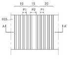
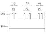
도 1을 참조하면, 기판 상에 동일한 선폭을 가지며, 서로 다른 피치를 가지는 라인 형태의 활성 패턴들(10, 15, 20)이 형성될 수 있다. 활성 패턴들(10, 15, 20) 사이는 소자 분리층(103)으로 채워질 수 있다. 소자 분리층(103)은 활성 패턴들(10, 15, 20) 사이를 소정의 높이로 채우고, 활성 패턴들(10, 15, 20)의 상부는 소자 분리층(103) 상으로 돌출될 수 있다. 활성 패턴들(10, 15, 20)의 선폭은 상용화된 포토리소그래피 장비의 해상도 한계 이하의 값일 수 있다. 제1 피치(P1)를 가지는 제1 활성 패턴들(10, 20)을 포함하고, 제1 활성 패턴들(10, 20)에 인접하여 배치된, 제2 피치(P2)를 가지는 제2 활성 패턴들(15)을 포함할 수 있다. 제2 피치(P2)는 제1 피치(P1)보다 넓을 수 있다. 제1 피치는 30nm 내지 35nm 범위에서 형성될 수 있다. 제2 피치는 40nm 내지 50nm 범위에서 형성될 수 있다. 제1 활성 패턴들(10, 20)은 4중 패터닝 기술(Quadruple Patterning Technology, QPT)을 이용하여 형성되며, 제2 활성 패턴들(15)은 2중 패터닝 기술(Double Patterning Technology, DPT)을 이용하여 형성될 수 있다.
Referring to FIG. 1 , line-shaped
도 2a 내지 도 2j는 본 발명의 일 실시예에 따른 반도체 소자 내의 패턴을 제조 하는 방법을 단계적으로 설명하기 위한 단면도들이다. 도 2a 내지 도 2j는 도 1의 절단선 A-A'에 대응하는 부분이 도시된다.
2A to 2J are cross-sectional views for explaining step by step a method of manufacturing a pattern in a semiconductor device according to an embodiment of the present invention. 2A to 2J show portions corresponding to the cut line A-A' of FIG. 1 .
도 2a를 참조하면, 기판(101) 상에 제1 하드 마스크층(105), 제2 하드 마스크층(110), 제3 하드 마스크층(115), 제1 희생층(121), 제1 반사방지층(125), 제2 희생층(141) 및 제2 반사방지층(145)를 순차적으로 형성할 수 있다.Referring to FIG. 2A , the first
기판(101)은 실리콘 웨이퍼와 같은 통상의 반도체 기판일 수 있다. 또한, 기판(101)은 SOI(Silicon On Insulator) 기판일 수 있다.The
제1 내지 제3 하드 마스크층(105, 110, 115)은 각각 실리콘 산화물(SiOx), 실리콘 산질화물(SiON), 실리콘 질화물(SixNy), TEOS(TetraEthylOthoSilicate) 또는 다결정질 실리콘 등과 같은 실리콘 함유 물질, ACL(amorphous carbon layer) 또는 SOH(Spin-On Hardmask)와 같이 탄소 함유물질 또는 금속 중 적어도 하나로 이루어질 수도 있다. 예를 들어, 제1 하드 마스크층(105)은 실리콘 질화물로 이루어질 수 있고, 상기 실리콘 질화물의 하부에 얇은 실리콘 산화물을 더 포함할 수 있다. 제2 하드 마스크층(110)은 실리콘 산화물로 이루어질 수 있다. 제3 하드 마스크층(115)는 다결정질 실리콘으로 이루어질 수 있다.The first to third hard mask layers 105 , 110 , and 115 are, respectively, such as silicon oxide (SiOx ), silicon oxynitride (SiON), silicon nitride (Six Ny ), TetraEthylOthoSilicate (TEOS), polycrystalline silicon, or the like. It may be made of at least one of a silicon-containing material, a carbon-containing material such as an amorphous carbon layer (ACL) or a spin-on hardmask (SOH) or a metal. For example, the first
제1 및 제2 희생층(121, 141)은 후속의 공정에서 제1 스페이서들(150s), 제2 스페이서들(160a) 및 제3 스페이서(160d)을 형성하기 위한 층들이다(도 2c 및 도 2g 참조). 제1 및 제2 희생층(121, 141)은 다결정질 실리콘, ACL(amorphous carbon layer) 또는 SOH(Spin-On Hardmask) 중에서 어느 하나를 포함할 수 있다.The first and second
제1 및 제2 반사방지층(125, 145)은 사진 식각 공정(photolithography process) 시에 하부막질에 의한 빛의 반사를 방지하기 위한 층들이다. 제1 및 제2 반사 방지층(125, 145)은 실리콘 산질화막(SiON)으로 이루어질 수 있다.The first and second
하드 마스크층들(105, 110, 115), 희생층들(121, 141) 및 반사 방지층들(125, 145)은 원자층 증착법(Atomic Layer Deposition, ALD), 화학 기상 증착법(Chemical Vapor Deposition, CVD) 또는 스핀 코팅 (spin coating) 등의 공정에 의해 형성될 수 있으며, 물질에 따라 베이크(bake) 공정이나 경화 공정이 추가될 수도 있다.The hard mask layers 105 , 110 , 115 , the
다음으로, 제2 희생층(141) 상에 감광막(photoresist, PR)을 덮고, 사진 식각 공정을 통해 라인 형태의 제1 감광막 패턴들(180p)을 형성할 수 있다.
Next, a photoresist (PR) may be covered on the second
도 2b를 참조하면, 제1 감광막 패턴들(180p)을 식각 마스크로 이용하여 제2 반사 방지층(145) 및 제2 희생층(141)을 이방성 식각함으로써, 제1 희생층(121) 상에 라인 형태의 제1 맨드럴들(mandrel, 140)을 형성할 수 있다.
Referring to FIG. 2B , the
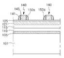
도 2c를 참조하면, 제1 맨드럴들(140)의 측벽에 제1 스페이서들(150s)을 형성할 수 있다.Referring to FIG. 2C ,
구체적으로, 제1 맨드럴들(140)을 콘포멀(conformal)하게 덮는 제1 스페이서 물질층을 형성한 후, 에치백(etchback) 공정을 수행함으로써 제1 맨드럴들(140)의 측벽에 제1 스페이서들(150s)을 형성할 수 있다. 상기 제1 스페이서 물질층의 두께는 최종적으로 형성하고자 하는 제1 활성 패턴들(10, 20, 도 1 참조) 사이의 간격을 고려하여 결정될 수 있다. 최종적으로 형성하고자 하는 제1 활성 패턴들(10, 20) 사이의 간격은 상용화된 포토리소그래피 장비의 해상도 한계보다 좁을 수 있다.Specifically, after forming a first spacer material layer that conformally covers the
상기 제1 스페이서 물질층은 제1 맨드럴들(140)과 식각 선택성을 가지는 물질로 이루어질 수 있다. 예를 들어, 제1 맨드럴들(140)이 다결정질 실리콘, ACL(amorphous carbon layer) 또는 SOH(Spin-On Hardmask) 중에서 어느 하나로 이루어진 경우, 상기 제1 스페이서 물질층은 실리콘 산화물 또는 실리콘 질화물로 이루어질 수 있다. 제1 스페이서 물질층은 원자층 증착법(ALD)에 의해 형성될 수 있다.
The first spacer material layer may be formed of a material having etch selectivity to the
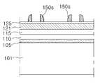
도 2d를 참조하면, 제1 맨드럴들(140)을 선택적으로 제거함으로써, 제1 희생층(121) 상에 라인 형태로 잔존하는 제1 스페이서들(150s)을 형성할 수 있다. 특정한 식각 조건에서 제1 스페이서들(150s)은 제1 맨드럴들(140)에 대해 식각 선택성을 가지므로, 제1 맨드럴들(140)을 선택적으로 제거할 수 있다.
Referring to FIG. 2D , by selectively removing the
도 2e를 참조하면, 제1 희생층(121) 상에 제1 스페이서들(150s)로부터 이격되고, 제1 맨들럴들(140)이 제거된 영역 밖에 위치하는 제2 감광막 패턴(190p)를 형성할 수 있다.Referring to FIG. 2E , a
제2 감광막 패턴(190p)의 선폭(W2)은 제1 스페이서들(150s)의 선폭(W1)보다 클 수 있다. 제2 감광막 패턴(190p)의 선폭(W2)은 최종적으로 형성하고자 하는 제2 활성 패턴들(15, 도 1 참조) 사이의 간격을 고려하여 결정될 수 있다.The line width W2 of the
최인접 제1 스페이서들(150s) 간의 간격은 제1 맨드럴(140)의 선폭과 실질적으로 동일할 수 있다. 제1 스페이서(150s)와 제2 감광막 패턴(190p) 간의 간격(S2)는 최인접 제1 스페이서들(150s)들 간의 간격(S1)과 실질적으로 동일할 수 있다. 실시예에 따라, 제2 감광막 패턴(190p)의 선폭(W2)을 감소시킬 수 있고, 제1 스페이서(150s)와 제2 감광막 패턴(190p) 간의 간격(S2)는 최인접 제1 스페이서들(150s)들 간의 간격(S1)과 보다 클 수 있다. 제2 감광막 패턴(190p)의 선폭(W2)는 최종적으로 제2 활성 패턴들(15)의 피치(P2)를 결정하게 되므로, 제2 감광막 패턴(190p)의 선폭(W2)를 조절함으로써, 제2 활성 패턴들(15)의 피치(P2)를 자유롭게 변화시킬 수 있다.
A distance between the adjacent
도 2f를 참조하면, 제3 하드 마스크층(115) 상에 제2 맨드럴들(120a)과 제3 맨드럴(120d)을 형성할 수 있다.Referring to FIG. 2F , the
제1 스페이서들(150s) 및 제2 감광막 패턴(190p)을 식각 마스크로 이용하여 제1 반사방지층(125) 및 제1 희생층(121)을 식각함으로써, 제3 하드 마스크층(115) 상에 제2 맨드럴들(120a) 및 제3 맨드럴(120d)를 형성할 수 있다.The
제1 스페이서들(150s)에 대응되는 위치에 제2 맨드럴들(120a)이 형성되며, 제2 감광막 패턴(190p)에 대응되는 위치에 제3 맨드럴(120d)이 형성될 수 있다.
The
도 2g를 참조하면, 제2 및 제3 맨드럴(120a, 120d)의 측벽에 제2 및 제3 스페이서들(160a, 160d)을 형성할 수 있다.Referring to FIG. 2G , second and
구체적으로, 제2 및 제3 맨드럴들(120a, 120d)을 콘포멀(conformal)하게 덮는 제2 스페이서 물질층을 형성한 후 에치백(etchback) 공정을 수행함으로써, 제2 맨드럴들(120a)의 측벽에 제2 스페이서들(160a)을 형성하고, 제3 맨드럴들(120d)의 측벽에 제3 스페이서들(160d)을 형성할 수 있다. 상기 제2 스페이서 물질층의 두께는 최종적으로 형성하고자 하는 활성 패턴들의 선폭을 고려하여 결정될 수 있다. 최종적으로 형성하고자 하는 활성 패턴들의 선폭은 상용화된 포토리소그래피 장비의 해상도 한계보다 작을 수 있다.Specifically, by forming a second spacer material layer that conformally covers the second and
제2 스페이서 물질층은 제2 및 제3 맨드럴들(120a, 120d)과 식각 선택성을 가지는 물질로 이루어질 수 있다. 예를 들어, 제2 및 제3 맨드럴들(120a, 120d)이 다결정질 실리콘, ACL(amorphous carbon layer) 또는 SOH(Spin-On Hardmask) 중에서 어느 하나로 이루어진 경우, 상기 제2 스페이서 물질층은 실리콘 산화물 또는 실리콘 질화물로 이루어질 수 있다. 제2 스페이서 물질층은 원자층 증착법(ALD)에 의해 형성될 수 있다.
The second spacer material layer may be formed of a material having etch selectivity to the second and
도 2h를 참조하면, 제2 및 제3 맨드럴들(120a, 120d)을 선택적으로 제거함으로써, 제3 하드 마스크층(115) 상에 라인 형태로 잔존하는 제2 및 제3 스페이서들(160a, 160d)을 형성할 수 있다. 특정한 식각 조건에서 제2 및 제3 스페이서들(160a, 160d)은 제2 및 제3 맨드럴들(120a, 120d)에 대해 식각 선택성을 가지므로, 제2 및 제3 맨드럴들(120a, 120d)을 선택적으로 제거할 수 있다.Referring to FIG. 2H , by selectively removing the second and
제2 맨드럴들(120a)을 제거함으로써, 라인 형태로 잔존하는 제2 스페이서들(160a)가 형성될 수 있고, 제3 맨드럴들(120d)을 제거함으로써, 라인 형태로 잔존하는 제3 스페이서들(160d)가 형성될 수 있다.By removing the second mandrels 120a,
제2 스페이서들(160a) 및 제3 스페이서들(160d)은 서로 다른 피치를 가질 수 있다. 제3 스페이서들(160d)의 피치(P2)가 제2 스페이서들(160a)의 피치(P1)보다 더 넓을 수 있다.The
제2 스페이서들(160a)의 피치(P1)는 제1 스페이서(150s)의 선폭에 의해 결정되고, 제3 스페이서들(160d)의 피치(P2)는 제2 감광막 패턴(190p)의 선폭에 의해 결정될 수 있다.
The pitch P1 of the
도 2i를 참조하면, 제2 및 제3 스페이서들(160a, 160d)을 식각 마스크로 이용하여 제1 내지 제3 하드 마스크층들(105, 110, 115) 및 기판(101)의 적어도 일부를 이방성 식각함으로써, 기판(101) 상에 서로 다른 피치를 가지는 제1 활성 패턴(10, 20) 및 제2 활성 패턴들(15)을 형성할 수 있다.Referring to FIG. 2I , the first to third hard mask layers 105 , 110 , 115 and at least a portion of the
기판(101)을 이방성 식각하는 단계에 의해, 제2 스페이서들(160a)이 기판(101)에 전사되어 제1 활성 패턴들(10, 20)이 형성되고, 제3 스페이서들(160d)이 기판(101)에 전사되어 제2 활성 패턴들(15)이 형성될 수 있다.By anisotropically etching the
먼저, 서로 다른 피치를 가지는 상기 제2 및 제3 스페이서들(160a, 160d)을 식각 마스크로 이용하여 하드 마스크층들을 식각함으로써 서로 다른 피치를 가지는 하드 마스크 패턴들을 형성할 수 있다. 이어서, 상기 하드 마스크 패턴들을 식각 마스크로 이용하여 기판(101)을 이방성 식각함으로써 제1 피치를 가지는 제1 활성 패턴들(10, 20) 및 상기 제1 피치보다 넓은 제2 피치를 가지는 제2 활성 패턴들(15)을 형성할 수 있다. 기판(101)의 이방성 식각이 완료된 후에, 제1 하드 마스크층(105)이 활성 패턴들(10, 15, 20)의 상부에 잔존할 수 있다.First, hard mask patterns having different pitches may be formed by etching the hard mask layers using the second and
상기 제1 피치는 30nm 내지 35nm 범위이고, 상기 제2 피치는 40nm 내지 50nm 범위일 수 있다.
The first pitch may be in a range of 30 nm to 35 nm, and the second pitch may be in a range of 40 nm to 50 nm.
도 2j를 참조하면, 제1 활성 패턴(10, 20) 및 제2 활성 패턴(15)의 상부가 돌출되도록 소자 분리층(103)을 형성할 수 있다.Referring to FIG. 2J , the
먼저, 기판(201)을 이방성 식각하여 형성된 활성 패턴들 사이의 얕은 트렌치(shallow trench)를 매립하는 절연층을 형성한 후, 제1 하드 마스크층(205)이 드러나도록 평탄화 공정을 진행하여 예비 소자 분리층을 형성할 수 있다.First, an insulating layer filling a shallow trench between active patterns formed by anisotropically etching the
다음으로, 추가적으로 깊은 트렌치(deep trench)를 형성한 후, 상기 깊은 트렌치를 매립하도록 절연층을 형성할 수 있다. 다음으로, 제1 하드 마스크층(205)가 노출되도록 평탄화 공정을 수행하여 소자 분리층(203)을 형성할 수 있다. 다만, 본 발명은 이에 한정되지 않으며, 실시예에 따라, 깊은 트렌치가 형성하지 않을 수 있다.Next, after additionally forming a deep trench, an insulating layer may be formed to fill the deep trench. Next, the
상기 절연층은 BPSG(Boron-Phosphor Slilicate Glass), HDP(High Density Plasma), FOX(Flowable OXide), TOSZ(TOnen SilaZene), SOG(Spin On Glass), USG(Undoped Silica Glass), TEOS(TetraEthyl Ortho Silicate), LTO(Low Temperature Oxide) 중 적어도 어느 하나로 이루어질 수 있다. 상기 평탄화 공정은 화학적 기계적 연마(CMP) 공정 의해 수행될 수 있다.The insulating layer is BPSG (Boron-Phosphor Slilicate Glass), HDP (High Density Plasma), FOX (Flowable OXide), TOSZ (TOnen SilaZene), SOG (Spin On Glass), USG (Undoped Silica Glass), TEOS (TetraEthyl Ortho) Silicate) and LTO (Low Temperature Oxide) may be made of at least one. The planarization process may be performed by a chemical mechanical polishing (CMP) process.
다음으로, 제1 및 제2 활성 패턴들(30, 35, 40)의 상부에 잔존하는 제1 하드 마스크층(205)을 선택적으로 제거한 후, 제1 및 제2 활성 패턴들(30, 35, 40)의 상부가 돌출되도록 소자 분리층(203)을 소정의 깊이로 식각할 수 있다. 이때, 제1 및 제2 활성 패턴들(30, 35, 40)의 상면 및 양 측면의 일부가 노출될 수 있다.
Next, after selectively removing the first
상기 도 2a 내지 도 2j를 참조하여 설명한 본 발명의 일 실시예에 따르면, 제1 활성 패턴들(10, 20)은 4중 패터닝 기술(QPT)에 의해 30nm 내지 35nm 범위의 피치로 형성되고, 제2 활성 패턴들(15)은 2중 패터닝 기술(DPT)에 의해 제1 활성 패턴들(10, 20)보다 더 넓은 피치를 갖도록 형성될 수 있다. 제2 활성 패턴들(15)의 피치는 40nm 내지 50nm 범위일 수 있다.According to an embodiment of the present invention described with reference to FIGS. 2A to 2J, the first
이와 같이, 4중 패턴 기술(QPT)와 2중 패턴 기술(DPT)를 함께 이용하여 반도체 소자 내에 동일한 선폭을 가지며, 서로 다른 피치를 가지는 활성 패턴들을 용이하게 형성할 수 있다. 반면, 4중 패턴 기술(QPT)만을 이용하면, 하나의 감광막 패턴으로부터 항상 고정된 피치를 가지는 2 쌍의 활성 패턴들을 형성되므로, 서로 다른 피치를 가지는 활성 패턴들을 형성하는 것이 용이하지 않다.
In this way, active patterns having the same line width and different pitches can be easily formed in a semiconductor device by using the quadruple pattern technology (QPT) and the double pattern technology (DPT) together. On the other hand, if only the quadruple pattern technology (QPT) is used, since two pairs of active patterns having a fixed pitch are always formed from one photoresist pattern, it is not easy to form active patterns having different pitches.
도 3은 본 발명의 일 실시예에 따른 반도체 소자 내의 패턴을 도시하는 평면도이다.
3 is a plan view illustrating a pattern in a semiconductor device according to an embodiment of the present invention.
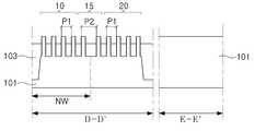
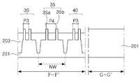
도 3을 참조하면, 기판 상에 동일한 선폭을 가지며, 서로 다른 피치를 가지는 라인 형태의 활성 패턴들(30, 35, 40)이 형성될 수 있다. 활성 패턴들(30, 35, 40)의 선폭은 상용화된 포토리소그래피 장비의 해상도 한계 이하의 값일 수 있다. 제1 피치(P3)를 가지는 제1 활성 패턴들(30, 40)을 포함하고, 제1 활성 패턴들(30, 40)에 인접하여 배치된, 제2 피치(P2)를 가지는 제2 활성 패턴들(35)을 포함할 수 있다. 제2 피치(P2)는 제1 피치(P1)보다 넓을 수 있다. 제1 피치는 30nm 내지 35nm 범위에서 형성될 수 있다. 제2 피치는 40nm 내지 50nm 범위에서 형성될 수 있다. 제1 활성 패턴들(30, 40)은 4중 패터닝 기술(Quadruple Patterning Technology, QPT)을 이용하여 형성되며, 제2 활성 패턴들(35)은 2중 패터닝 기술(Double Patterning Technology, DPT)을 이용하여 형성될 수 있다.Referring to FIG. 3 , line-shaped
활성 패턴들(30, 35, 40) 사이는 소자 분리층(203)으로 채워질 수 있다. 소자 분리층(203)은 활성 패턴들(30, 35, 40) 사이를 소정의 높이로 채우고, 활성 패턴들(30, 35, 40)의 상부는 소자 분리층(203) 상으로 돌출될 수 있다.
An
도 4a 내지 도 4j는 본 발명의 일 실시예에 따른 반도체 소자 내의 패턴 형성 방법을 단계적으로 설명하기 위한 단면도들이다. 도 4a 내지 도 4j는 도 3의 절단선 B-B'에 대응하는 부분이 도시된다.
4A to 4J are cross-sectional views for explaining step by step a method of forming a pattern in a semiconductor device according to an embodiment of the present invention. 4A to 4J are portions corresponding to the cut line B-B' of FIG. 3 .
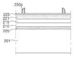
도 4a를 참조하면, 기판(201) 상에 제1 하드 마스크층(205), 제2 하드 마스크층(210), 제3 하드 마스크층(215), 제1 희생층(221), 제1 반사방지층(225), 제2 희생층(241) 및 제2 반사방지층(245)를 순차적으로 형성할 수 있다.Referring to FIG. 4A , a first
기판(201)은 실리콘 웨이퍼와 같은 통상의 반도체 기판일 수 있다. 또한, 기판(201)은 SOI(Silicon On Insulator) 기판일 수 있다.The
제1 내지 제3 하드 마스크층(205, 210, 215)은 각각 실리콘 산화물(SiOx), 실리콘 산질화물(SiON), 실리콘 질화물(SixNy), TEOS(TetraEthylOthoSilicate) 또는 다결정질 실리콘 등과 같은 실리콘 함유 물질, ACL(amorphous carbon layer) 또는 SOH(Spin-On Hardmask)와 같이 탄소 함유물질 또는 금속 중 적어도 하나로 이루어질 수도 있다. 예를 들어, 제1 하드 마스크층(205)은 실리콘 질화물로 이루어질 수 있고, 상기 실리콘 질화물의 하부에 얇은 실리콘 산화물을 더 포함할 수 있다. 제2 하드 마스크층(210)은 실리콘 산화물로 이루어질 수 있다. 제3 하드 마스크층(215)는 다결정질 실리콘으로 이루어질 수 있다.The first to third hard mask layers 205 , 210 , and 215 are, respectively, silicon oxide (SiOx ), silicon oxynitride (SiON), silicon nitride (Six Ny ), TetraEthylOthoSilicate (TEOS), polycrystalline silicon, or the like. It may be made of at least one of a silicon-containing material, a carbon-containing material such as an amorphous carbon layer (ACL) or a spin-on hardmask (SOH) or a metal. For example, the first
제1 및 제2 희생층(221, 241)은 후속의 공정에서 제1 스페이서들(250s), 제2 스페이서들(260a) 및 제3 스페이서(260d)을 형성하기 위한 층들이다(도 4c 및 도 4g 참조). 제1 및 제2 희생층(221, 241)은 다결정질 실리콘, ACL(amorphous carbon layer) 또는 SOH(Spin-On Hardmask) 중에서 어느 하나를 포함할 수 있다.The first and second
제1 및 제2 반사방지층(225, 245)은 사진 식각 공정(photolithography process) 시에 하부막질에 의한 빛의 반사를 방지하기 위한 층들이다. 제1 및 제2 반사 방지층(225, 245)은 실리콘 산질화막(SiON)으로 이루어질 수 있다.
The first and second
하드 마스크층들(205, 210, 215), 희생층들(221, 241) 및 반사 방지층들(225, 245)은 원자층 증착법(Atomic Layer Deposition, ALD), 화학 기상 증착법(Chemical Vapor Deposition, CVD) 또는 스핀 코팅 (spin coating) 등의 공정에 의해 형성될 수 있으며, 물질에 따라 베이크(bake) 공정이나 경화 공정이 추가될 수도 있다.
The hard mask layers 205 , 210 , 215 , the
다음으로, 제2 희생층(241) 상에 감광막(photoresist, PR)을 덮고, 사진 식각 공정을 통해 라인 형태의 제1 감광막 패턴들(280p)을 형성할 수 있다.
Next, a photoresist (PR) may be covered on the second
도 4b를 참조하면, 제1 감광막 패턴들(280p)을 식각 마스크로 이용하여 제2 반사 방지층(245) 및 제2 희생층(241)을 이방성 식각함으로써, 제1 희생층(221) 상에 제1 맨드럴들(mandrel, 240)을 형성할 수 있다.
Referring to FIG. 4B , the
도 4c를 참조하면, 제1 맨드럴들(240)의 측벽에 제1 스페이서들(250s)을 형성할 수 있다.Referring to FIG. 4C ,
구체적으로, 제1 맨드럴들(240)을 콘포멀(conformal)하게 덮는 제1 스페이서 물질층을 형성한 후, 에치백(etchback) 공정을 수행함으로써 제1 맨드럴들(240)의 측벽에 제1 스페이서들(250s)을 형성할 수 있다. 상기 제1 스페이서 물질층의 두께는 최종적으로 형성하고자 하는 제1 활성 패턴들(30, 40, 도 1 참조) 사이의 간격을 고려하여 결정될 수 있다. 최종적으로 형성하고자 하는 제1 활성 패턴들(30, 40) 사이의 간격은 상용화된 포토리소그래피 장비의 해상도 한계보다 좁을 수 있다.Specifically, after forming a first spacer material layer that conformally covers the
상기 제1 스페이서 물질층은 제1 맨드럴들(240)과 식각 선택성을 가지는 물질로 이루어질 수 있다. 예를 들어, 제1 맨드럴들(240)이 다결정질 실리콘, ACL(amorphous carbon layer) 또는 SOH(Spin-On Hardmask) 중에서 어느 하나로 이루어진 경우, 상기 제1 스페이서 물질층은 실리콘 산화물 또는 실리콘 질화물로 이루어질 수 있다. 제1 스페이서 물질층은 원자층 증착법(ALD)에 의해 형성될 수 있다.
The first spacer material layer may be formed of a material having etch selectivity to the
도 4d를 참조하면, 제1 맨드럴들(240)을 선택적으로 제거함으로써, 제1 희생층(221) 상에 라인 형태로 잔존하는 제1 스페이서들(250s)을 형성할 수 있다. 특정한 식각 조건에서 제1 스페이서들(250s)은 제1 맨드럴들(240)에 대해 식각 선택성을 가지므로, 제1 맨드럴들(240)을 선택적으로 제거할 수 있다.
Referring to FIG. 4D , by selectively removing the
도 4e를 참조하면, 제1 희생층(221) 상에 제1 스페이서들(250s)로부터 이격되고, 제1 맨들럴(240)이 제거된 영역 내에 위치하는 제2 감광막 패턴(290p)를 형성할 수 있다.Referring to FIG. 4E , on the first
제2 감광막 패턴(290p)의 선폭(W2)은 제1 스페이서들(250s)의 선폭(W1)보다 넓을 수 있다. 제2 감광막 패턴(290p)의 선폭(W2)은 최종적으로 형성하고자 하는 제2 활성 패턴들(35, 도 1 참조) 사이의 간격을 고려하여 결정될 수 있다.The line width W2 of the
본 실시예에서, 양 측의 제1 스페이서(250s)와 제2 감광막 패턴(290p) 사이의 간격(S)은 실질적으로 동일할 수 있다.In this embodiment, the distance S between the
실시예에 따라, 제2 감광막 패턴(290p)의 선폭(W2)을 감소시키거나 증가시킬 수 있다. 제2 감광막 패턴(290p)의 선폭(W2)는 최종적으로 제2 활성 패턴들(35)의 피치(P2)를 결정하게 되므로, 제2 감광막 패턴(290p)의 선폭(W2)를 조절함으로써, 제2 활성 패턴들(35)의 피치(P2)를 자유롭게 변화시킬 수 있다.
In some embodiments, the line width W2 of the
도 4f를 참조하면, 제3 하드 마스크층(215) 상에 제2 맨드럴들(220a)과 제3 맨드럴(220d)을 형성할 수 있다.Referring to FIG. 4F , the
제1 스페이서들(250s) 및 제2 감광막 패턴(290p)을 식각 마스크로 이용하여 제1 반사방지층(225) 및 제1 희생층(221)을 식각함으로써, 제3 하드 마스크층(215) 상에 제2 맨드럴들(220a) 및 제3 맨드럴(220d)를 형성할 수 있다.The
제1 스페이서들(250s)에 대응되는 위치에 제2 맨드럴들(220a)이 형성되며, 제2 감광막 패턴(290p)에 대응되는 위치에 제3 맨드럴(220d)이 형성될 수 있다.
The
도 4g를 참조하면, 제2 및 제3 맨드럴(220a, 220d)의 측벽에 각각 제2 및 제3 스페이서들(260a, 260d)을 형성할 수 있다.Referring to FIG. 4G , second and
구체적으로, 제2 및 제3 맨드럴들(220a, 220d)을 콘포멀(conformal)하게 덮는 제2 스페이서 물질층을 형성한 후 에치백(etchback) 공정을 수행함으로써, 제2 맨드럴들(220a)의 측벽에 제2 스페이서들(260a)을 형성하고, 제3 맨드럴들(220d)의 측벽에 제3 스페이서들(260d)을 형성할 수 있다. 상기 제2 스페이서 물질층의 두께는 최종적으로 형성하고자 하는 활성 패턴들의 선폭을 고려하여 결정될 수 있다. 최종적으로 형성하고자 하는 활성 패턴들의 선폭은 상용화된 포토리소그래피 장비의 해상도 한계보다 작을 수 있다.Specifically, by forming a second spacer material layer that conformally covers the second and
제2 스페이서 물질층은 제2 및 제3 맨드럴들(220a, 220d)과 식각 선택성을 가지는 물질로 이루어질 수 있다. 예를 들어, 제2 및 제3 맨드럴들(220a, 220d)이 다결정질 실리콘, ACL(amorphous carbon layer) 또는 SOH(Spin-On Hardmask) 중에서 어느 하나로 이루어진 경우, 상기 제2 스페이서 물질층은 실리콘 산화물 또는 실리콘 질화물로 이루어질 수 있다. 제2 스페이서 물질층은 원자층 증착법(ALD)에 의해 형성될 수 있다.
The second spacer material layer may be formed of a material having etch selectivity to the second and
도 4h를 참조하면, 제2 및 제3 맨드럴들(220a, 220d)을 선택적으로 제거함으로써, 제3 하드 마스크층(215) 상에 라인 형태로 잔존하는 제2 및 제3 스페이서들(260a, 260d)을 형성할 수 있다. 특정한 식각 조건에서 제2 및 제3 스페이서들(260a, 260d)은 제2 및 제3 맨드럴들(220a, 220d)에 대해 식각 선택성을 가지므로, 제2 및 제3 맨드럴들(220a, 220d)을 선택적으로 제거할 수 있다.Referring to FIG. 4H , by selectively removing the second and
제2 맨드럴들(220a)을 제거함으로써, 라인 형태로 잔존하는 제2 스페이서들(260a)가 형성될 수 있고, 제3 맨드럴들(220d)을 제거함으로써, 라인 형태로 잔존하는 제3 스페이서들(260d)가 형성될 수 있다.By removing the second mandrels 220a,
제2 스페이서들(260a) 및 제3 스페이서들(260d)은 서로 다른 피치를 가질 수 있다. 제3 스페이서들(260d)의 피치(P2)가 제2 스페이서들(260a)의 피치(P1)보다 더 넓을 수 있다.The
제2 스페이서들(260a)의 피치(P1)는 제1 스페이서(250s)의 선폭에 의해 결정되고, 제3 스페이서들(260d)의 피치(P2)는 제2 감광막 패턴(290p)의 선폭에 의해 결정될 수 있다.
The pitch P1 of the
도 4i를 참조하면, 제2 및 제3 스페이서들(260a, 260d)을 식각 마스크로 이용하여 제1 내지 제3 하드 마스크층들(205, 210, 215) 및 기판(201)의 적어도 일부를 이방성 식각함으로써, 기판(201) 상에 서로 다른 피치를 가지는 제1 활성 패턴(30, 40) 및 제2 활성 패턴들(35)을 형성할 수 있다. 기판(201)을 이방성 식각하는 단계에 의해, 제2 스페이서들(260a)이 기판(201)에 전사되어 제1 활성 패턴들(30, 40)이 형성되고, 제3 스페이서들(260d)이 기판(201)에 전사되어 제2 활성 패턴들(35)이 형성될 수 있다.Referring to FIG. 4I , the first to third hard mask layers 205 , 210 , and 215 and at least a portion of the
먼저, 서로 다른 피치를 가지는 상기 제2 및 제3 스페이서들(260a, 260d)을 식각 마스크로 이용하여 하드 마스크층들을 식각함으로써 서로 다른 피치를 가지는 하드 마스크 패턴들을 형성할 수 있다. 이어서, 상기 하드 마스크 패턴들을 식각 마스크로 이용하여 기판(201)을 이방성 식각함으로써 제1 피치를 가지는 제1 활성 패턴들(30, 40) 및 상기 제1 피치보다 넓은 제2 피치를 가지는 제2 활성 패턴들(35)을 형성할 수 있다. 기판(201)의 이방성 식각이 완료된 후에, 제1 하드 마스크층(205)이 활성 패턴들(30, 35, 40)의 상부에 잔존할 수 있다.First, hard mask patterns having different pitches may be formed by etching the hard mask layers using the second and
상기 제1 피치는 30nm 내지 35nm 범위이고, 상기 제2 피치는 40nm 내지 50nm 범위일 수 있다.
The first pitch may be in a range of 30 nm to 35 nm, and the second pitch may be in a range of 40 nm to 50 nm.
도 4j를 참조하면, 제1 활성 패턴(30, 40) 및 제2 활성 패턴(35)의 상부가 돌출되도록 소자 분리층(203)을 형성할 수 있다.Referring to FIG. 4J , the
먼저, 기판(201)을 이방성 식각하여 형성된 활성 패턴들 사이의 얕은 트렌치(shallow trench)를 매립하는 절연층을 형성한 후, 제1 하드 마스크층(205)이 드러나도록 평탄화 공정을 진행하여 예비 소자 분리층을 형성할 수 있다.First, an insulating layer filling a shallow trench between active patterns formed by anisotropically etching the
다음으로, 추가적으로 깊은 트렌치(deep trench)를 형성한 후, 상기 깊은 트렌치를 매립하도록 절연층을 형성할 수 있다. 다음으로, 제1 하드 마스크층(205)가 노출되도록 평탄화 공정을 수행하여 소자 분리층(203)을 형성할 수 있다. 다만, 본 발명은 이에 한정되지 않으며, 실시예에 따라, 깊은 트렌치가 형성하지 않을 수 있다.Next, after additionally forming a deep trench, an insulating layer may be formed to fill the deep trench. Next, the
상기 절연층은 BPSG(Boron-Phosphor Slilicate Glass), HDP(High Density Plasma), FOX(Flowable OXide), TOSZ(TOnen SilaZene), SOG(Spin On Glass), USG(Undoped Silica Glass), TEOS(TetraEthyl Ortho Silicate), LTO(Low Temperature Oxide) 중 적어도 어느 하나로 이루어질 수 있다. 상기 평탄화 공정은 화학적 기계적 연마(CMP) 공정 의해 수행될 수 있다.The insulating layer is BPSG (Boron-Phosphor Slilicate Glass), HDP (High Density Plasma), FOX (Flowable OXide), TOSZ (TOnen SilaZene), SOG (Spin On Glass), USG (Undoped Silica Glass), TEOS (TetraEthyl Ortho) Silicate) and LTO (Low Temperature Oxide) may be made of at least one. The planarization process may be performed by a chemical mechanical polishing (CMP) process.
다음으로, 제1 및 제2 활성 패턴들(30, 35, 40)의 상부에 잔존하는 제1 하드 마스크층(205)을 선택적으로 제거한 후, 제1 및 제2 활성 패턴들(30, 35, 40)의 상부가 돌출되도록 소자 분리층(203)을 소정의 깊이로 식각할 수 있다. 이때, 제1 및 제2 활성 패턴들(30, 35, 40)의 상면 및 양 측면의 일부가 노출될 수 있다.
Next, after selectively removing the first
상기 도 4a 내지 도 4j를 참조하여 설명한 본 발명의 일 실시예에 따르면, 제1 활성 패턴들(30, 40)은 4중 패터닝 기술(QPT)에 의해 30nm 내지 35nm 범위의 피치로 형성되고, 제2 활성 패턴들(35)은 2중 패터닝 기술(DPT)에 의해 제1 활성 패턴들(30, 40)보다 더 넓은 피치를 갖도록 형성될 수 있다. 예를 들어, 제2 활성 패턴들은 40nm 내지 50nm 범위의 피치로 형성될 수 있다.According to an embodiment of the present invention described with reference to FIGS. 4A to 4J, the first
이와 같이, 4중 패턴 기술(QPT)와 2중 패턴 기술(DPT)를 함께 이용하여 반도체 소자 내에 동일한 선폭을 가지며, 서로 다른 피치를 가지는 활성 패턴들을 용이하게 형성할 수 있다. 반면, 4중 패턴 기술(QPT)만을 이용하면, 하나의 감광막 패턴으로부터 항상 고정된 피치를 가지는 2 쌍의 활성 패턴들을 형성되므로, 서로 다른 피치를 가지는 활성 패턴들을 형성하는 것이 용이하지 않다.
In this way, active patterns having the same line width and different pitches can be easily formed in a semiconductor device by using the quadruple pattern technology (QPT) and the double pattern technology (DPT) together. On the other hand, if only the quadruple pattern technology (QPT) is used, since two pairs of active patterns having a fixed pitch are always formed from one photoresist pattern, it is not easy to form active patterns having different pitches.
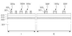
도 5는 본 발명의 일 실시예에 따른 반도체 소자 내의 패턴을 도시하는 평면도이다. 도 5에 도시된 반도체 소자는 제1 영역(I) 및 제2 영역(II)을 포함할 수 있다. 예를 들어, 도 5에서 제1 영역(I)은 로직(logic) 영역이고, 제2 영역(II)은 정적 랜덤 액세스 메모리(SRAM) 영역일 수 있다.
5 is a plan view illustrating a pattern in a semiconductor device according to an embodiment of the present invention. The semiconductor device illustrated in FIG. 5 may include a first region (I) and a second region (II). For example, in FIG. 5 , the first region I may be a logic region, and the second region II may be a static random access memory (SRAM) region.
도 5를 참조하면, 제1 영역(I)에는 기판(301) 상에 동일한 선폭을 가지며, 서로 다른 피치를 가지는 라인 형태의 활성 패턴들(50, 55, 60)이 형성될 수 있다. 활성 패턴들(50, 55, 60)의 선폭은 상용화된 포토리소그래피 장비의 해상도 한계 이하의 값일 수 있다. 제1 영역(I)은 제1 피치(P1')를 가지는 제1 활성 패턴들(50, 60)을 포함하고, 제1 활성 패턴들(50, 60)에 인접하여 배치된, 제2 피치(P2')를 가지는 제2 활성 패턴들(55)을 포함할 수 있다. 제2 피치(P2')는 제1 피치(P1')보다 넓을 수 있다. 제1 피치는 30nm 내지 35nm 범위에서 형성될 수 있다. 제2 피치는 40nm 내지 50nm 범위에서 형성될 수 있다. 제1 활성 패턴들(50, 60)은 4중 패터닝 기술(Quadruple Patterning Technology, QPT)을 이용하여 형성되며, 제2 활성 패턴들(55)은 2중 패터닝 기술(Double Patterning Technology, DPT)을 이용하여 형성될 수 있다.Referring to FIG. 5 , line-shaped
활성 패턴들(50, 55, 60) 사이는 소자 분리층(303)이 형성될 수 있다. 소자 분리층(303)은 활성 패턴들(50, 55, 60) 사이를 소정의 높이로 채우고, 활성 패턴들(50, 55, 60)의 상부는 소자 분리층(303) 상으로 돌출될 수 있다.
A
다시 도 5를 참조하면, 제2 영역(II)에는 기판(101) 상에 동일한 선폭을 가지며, 서로 다른 피치를 가지는 라인 형태의 활성 패턴들(70, 75, 80)이 형성될 수 있다. 활성 패턴들(70, 75, 80)의 선폭은 상용화된 포토리소그래피 장비의 해상도 한계 이하의 값일 수 있다. 제2 영역(II)에는 제3 피치(P3')를 가지는 제3 활성 패턴들(70, 80)을 포함하고, 제3 활성 패턴들(70, 80)에 인접하여 배치된, 제4 피치(P4')를 가지는 제4 활성 패턴들(75)을 포함할 수 있다. 제4 피치(P4')는 제3 피치(P3')보다 넓을 수 있다. 제2 영역(II)에 형성되는 활성 패턴들(70, 75, 80)은 2중 패터닝 기술(DPT)을 이용하여 형성될 수 있다.Referring back to FIG. 5 , line-shaped
활성 패턴들(70, 75, 80) 사이는 소자 분리층(303)이 형성될 수 있다. 소자 분리층(303)은 활성 패턴들(70, 75, 80) 사이를 소정의 높이로 채우고, 활성 패턴들(70, 75, 80)의 상부는 소자 분리층(303) 상으로 돌출될 수 있다.
A
도6a 내지 도 6i는 본 발명의 일 실시예에 따른 반도체 소자의 패턴 형성 방법을 단계적으로 설명하기 위한 단면도들이다. 도 6a 내지 도 6i는 도 5의 절단선 C-C'에 대응하는 부분이 도시된다.
6A to 6I are cross-sectional views for explaining step by step a method of forming a pattern of a semiconductor device according to an embodiment of the present invention. 6A to 6I show portions corresponding to the cut line C-C' of FIG. 5 .
도 6a를 참조하면, 기판(301) 상에 제1 하드 마스크층(305), 제2 하드 마스크층(310), 제3 하드 마스크층(315), 제1 희생층(321), 제1 반사방지층(325), 제2 희생층(341) 및 제2 반사방지층(345)를 순차적으로 형성할 수 있다.Referring to FIG. 6A , a first
기판(301)은 실리콘 웨이퍼와 같은 통상의 반도체 기판일 수 있다. 또한, 기판(301)은 SOI(Silicon On Insulator) 기판일 수 있다.The
제1 내지 제3 하드 마스크층(305, 310, 315)은 각각 실리콘 산화물(SiOx), 실리콘 산질화물(SiON), 실리콘 질화물(SixNy), TEOS(TetraEthylOthoSilicate) 또는 다결정질 실리콘 등과 같은 실리콘 함유 물질, ACL(amorphous carbon layer) 또는 SOH(Spin-On Hardmask)와 같이 탄소 함유물질 또는 금속 중 적어도 하나로 이루어질 수도 있다. 예를 들어, 제1 하드 마스크층(305)은 실리콘 질화물로 이루어질 수 있고, 상기 실리콘 질화물의 하부에 얇은 실리콘 산화물을 더 포함할 수 있다. 제2 하드 마스크층(310)은 실리콘 산화물로 이루어질 수 있다. 제3 하드 마스크층(315)는 다결정질 실리콘으로 이루어질 수 있다.The first to third hard mask layers 305 , 310 , and 315 are, respectively, such as silicon oxide (SiOx ), silicon oxynitride (SiON), silicon nitride (Six Ny ), TetraEthylOthoSilicate (TEOS), polycrystalline silicon, or the like. It may be made of at least one of a silicon-containing material, a carbon-containing material such as an amorphous carbon layer (ACL) or a spin-on hardmask (SOH) or a metal. For example, the first
제1 희생층(321)은 후속의 공정에서 제1 스페이서들(350s)을 형성하기 위한 층이고(도 6c 참조), 제2 희생층(341)은 후속의 공정에서 제2 및 제3 스페이서들(360a, 360d) 그리고 제4 및 제5 스페이서들(360f, 306g)을 형성하기 위한 층이다(도 6g 참조).The first
제1 및 제2 희생층(321, 341)은 다결정질 실리콘, ACL(amorphous carbon layer) 또는 SOH(Spin-On Hardmask) 중에서 어느 하나를 포함할 수 있다.The first and second
제1 및 제2 반사방지층(325, 345)은 사진 식각 공정 시에 하부막질에 의한 빛의 반사를 방지하기 위한 것으로써, 실리콘 산질화막(SiON)으로 이루어질 수 있다.The first and second
하드 마스크층들(305, 310, 315), 희생층들(321, 341) 및 반사방지층들(325, 345)은 원자층 증착법(Atomic Layer Deposition, ALD), 화학 기상 증착법(Chemical Vapor Deposition, CVD) 또는 스핀 코팅 (spin coating) 등의 공정에 의해 형성될 수 있으며, 물질에 따라 베이크(bake) 공정이나 경화 공정이 추가될 수도 있다.
The hard mask layers 305 , 310 , 315 , the
다음으로, 제2 희생층(341) 상에 감광막을 덮고, 사진 식각 공정을 통해 제1 영역(I)에 제1 감광막 패턴(380p)을 형성할 수 있다.
Next, a photoresist layer may be covered on the second
도 6b를 참조하면, 제1 감광막 패턴(380p)을 식각 마스크로 이용하여 제2 반사 방지층(345) 및 제2 희생층(341)을 이방성 식각함으로써, 제1 영역(I)에서 제1 희생층(321) 상에 라인 형태의 제1 맨드럴들(340)을 형성할 수 있다. 이때, 제2 영역(II)에서 제2 반사방지층(345) 및 제2 희생층(341)은 식각 공정에 의해 완전히 제거될 수 있다.
Referring to FIG. 6B , the
도 6c를 참조하면, 제1 영역(I)의 제1 맨드럴들(340)의 측벽에 제1 스페이서들(350s)을 형성할 수 있다.Referring to FIG. 6C ,
구체적으로, 제1 맨드럴들(340)을 콘포멀(conformal)하게 덮는 제1 스페이서 물질층을 형성한 후, 에치백(etchback)을 수행함으로써 제1 맨드럴들(340)의 측벽에 제1 스페이서들(350s)을 형성할 수 있다. 제1 스페이서 물질층의 두께는 최종적으로 형성하고자 하는 활성 패턴들의 간격을 고려하여 결정될 수 있다. 최종적으로 형성하고자 하는 활성 패턴들의 간격은 상용화된 포토리소그래피 장비의 해상도 한계보다 작을 수 있다.Specifically, after forming a first spacer material layer that conformally covers the
제1 스페이서 물질층은 제1 맨드럴들(340)과 식각 선택성을 가지는 물질로 이루어질 수 있다. 예를 들어, 제1 맨드럴들(340)이 다결정질 실리콘, ACL(amorphous carbon layer) 또는 SOH(Spin-On Hardmask) 중에서 어느 하나로 이루어진 경우, 제1 스페이서 물질층은 실리콘 산화물 또는 실리콘 질화물로 이루어질 수 있다. 제1 스페이서 물질층은 원자층 증착법(ALD)에 의해 형성될 수 있다.
The first spacer material layer may be formed of a material having etch selectivity to the
도 6d를 참조하면, 제1 영역(I)에서 제1 맨드럴들(340)을 선택적으로 제거함으로써, 제1 희생층(321) 상에 라인 형태로 잔존하는 제1 스페이서들(350s)을 형성할 수 있다. 특정한 식각 조건에서 제1 스페이서들(350s)은 제1 맨드럴들(340)에 대해 식각 선택성을 가지는 물질로 이루어질 수 있으므로, 제1 맨드럴들(340)을 선택적으로 제거할 수 있다.
Referring to FIG. 6D , by selectively removing the
도 6e를 참조하면, 제1 영역(I)에서 제1 희생층(321) 상에 제1 스페이서들(350s)로부터 이격되고, 제1 맨들럴들(340)이 제거된 영역 밖에 위치하는 제2 감광막 패턴(390p)를 형성하고, 제2 영역(II)에서 제1 희생층(321) 상에 서로 다른 선폭을 가지는 제3 및 제4 감광막 패턴(322p, 324p)을 형성할 수 있다.Referring to FIG. 6E , in the first region I, on the first
제2 내지 제4 감광막 패턴들(320p, 322p, 324p)의 선폭(W2, W3, W4)은 제1 스페이서들(350s)의 선폭(W1)보다 클 수 있다. 또한, 제4 감광막 패턴(324p)의 선폭(W4)은 제2 및 제3 감광막 패턴들(320p, 322p)의 선폭들(W2, W3)보다 클 수 있다.Line widths W2 , W3 , and W4 of the second to fourth photoresist layer patterns 320p , 322p , and 324p may be greater than the line width W1 of the
최인접 제1 스페이서들(350s) 간의 간격(S1)은 제1 맨드럴(340)의 선폭과 실질적으로 동일할 수 있다. 제1 스페이서(350s)와 제2 감광막 패턴(320p) 간의 간격(S2)는 최인접 제1 스페이서들(350s)들 간의 간격(S1)과 실질적으로 동일할 수 있다. 실시예에 따라, 제2 감광막 패턴(390p)의 선폭(W2)을 감소시킬 수 있고, 제1 스페이서(350s)와 제2 감광막 패턴(390p) 간의 간격(S2)는 최인접 제1 스페이서들(350s)들 간의 간격(S1)과 보다 클 수 있다. 제2 감광막 패턴(390p)의 선폭(W2)는 최종적으로 제2 활성 패턴들(55)의 피치(P2')를 결정하게 되므로, 제2 감광막 패턴(220p)의 선폭(W2)를 조절함으로써, 제2 활성 패턴들(55)의 피치(P2')를 자유롭게 변화시킬 수 있다.A distance S1 between the adjacent
또한, 제3 감광막 패턴들(392p)과 제4 감광막 패턴(394p) 사이의 간격(S3)은 제1 스페이서(350s)와 제2 감광막 패턴(390p) 간의 간격(S2)보다 클 수 있다.
Also, the distance S3 between the third
도 6f를 참조하면, 제1 영역(I)에서 제3 하드 마스크층(315) 상에 제2 맨드럴들(320a)과 제3 맨드럴(320d)을 형성하고, 제2 영역(II)에서 제3 하드 마스크층(315) 상에 제4 맨드럴(320f)와 제5 맨들럴(320g)를 형성할 수 있다.Referring to FIG. 6F ,
제1 영역(I)에서 제1 스페이서들(350s) 및 제2 감광막 패턴(390p)을 식각 마스크로 이용하여 제1 반사방지층(325) 및 제1 희생층(321)을 식각함으로써, 각각 제3 하드 마스크층(315) 상에 제2 맨드럴들(320a) 및 제3 맨드럴(320d)를 형성할 수 있다. 제2 영역(II)에서 상기 제3 감광막 패턴들(392p)및 제4 감광막 패턴(394p)을 식각 마스크로 이용하여 제1 반사방지층(325) 및 제1 희생층(321)을 식각함으로써, 각각 제3 하드 마스크층(315) 상에 제4 맨드럴(320f) 및 제5 맨드럴(320g)를 형성할 수 있다.In the first region I, the
제1 스페이서들(350s)에 대응되는 위치에 제2 맨드럴들(320a)이 형성되며, 제2 감광막 패턴(390p)에 대응되는 위치에 제3 맨드럴(320d)이 형성될 수 있다. 제3 감광막 패턴(392p)에 대응되는 위치에 제4 맨드럴(320f)이 형성되며, 제4 감광막 패턴(394p)에 대응되는 위치에 제5 맨드럴(320g)이 형성될 수 있다.
The
도 6g를 참조하면, 제2 내지 제5 맨드럴(320a, 320d, 320f, 320g)의 측벽에 제2 내지 제5 스페이서들(360a, 360d, 360f, 360g)을 형성할 수 있다.Referring to FIG. 6G , second to
구체적으로, 제2 내지 제5 맨드럴들(320a, 320d, 320f, 320g)을 콘포멀(conformal)하게 덮는 제2 스페이서 물질층을 형성한 후, 에치백(etchback)을 수행함으로써 제2 내지 제5 맨드럴들(320a, 320d, 320f, 320g)의 측벽에 제2 내지 제5 스페이서들(360a, 360d, 360f, 360g)을 형성할 수 있다. 제2 스페이서 물질층의 두께는 최종적으로 형성하고자 하는 활성 패턴들의 선폭을 고려하여 결정될 수 있다. 최종적으로 형성하고자 하는 활성 패턴들의 선폭은 상용화된 포토리소그래피 장비의 해상도 한계보다 작을 수 있다.Specifically, after forming a second spacer material layer that conformally covers the second to
상기 제2 스페이서 물질층은 제2 내지 제5 맨드럴들(320a, 320d, 320f, 320g)과 식각 선택성을 가지는 물질로 이루어질 수 있다. 예를 들어, 제2 내지 제5 맨드럴들(340)이 다결정질 실리콘, ACL(amorphous carbon layer) 또는 SOH(Spin-On Hardmask) 중에서 어느 하나로 이루어진 경우, 상기 제2 스페이서 물질층은 실리콘 산화물 또는 실리콘 질화물로 이루어질 수 있다. 제2 스페이서 물질층은 원자층 증착법(ALD)에 의해 형성될 수 있다.
The second spacer material layer may be formed of a material having etch selectivity to the second to
도 6h를 참조하면, 제2 내지 제5 맨드럴들(320a, 320d, 320f, 320g)을 선택적으로 제거함으로써, 제1 영역(I)에서 제3 하드 마스크층(115) 상에 라인 형태로 잔존하는 제2 스페이서들(360a) 및 제3 스페이서들(360d)을 형성할 수 있고, 제2 영역(II)에서 제4 스페이스들(360f) 및 제5 스페이서들(360g)을 형성할 수 있다. 특정한 식각 조건에서 제2 스페이서들(360a, 360d, 360f, 360g)은 제2 내지 제5 맨드럴들(320a, 320d, 320f, 320g)에 대해 식각 선택성을 가지므로, 제2 내지 제5 맨드럴들(320a, 320d, 320f, 320g)을 선택적으로 제거할 수 있다.Referring to FIG. 6H , by selectively removing the second to
제2 스페이서들(360a), 제3 스페이서들(360d), 제4 스페이서들(360f) 및 제5 스페이서들(360g)은 서로 다른 피치를 가질 수 있다. 제1 영역(I)에서 제2 및 제3 맨드럴들(320a, 320d)을 제거함으로써, 각각 제3 하드 마스크층(315) 상에 서로 다른 피치를 가지는 라인 형태의 제2 스페이서들(360a) 및 제3 스페이서들 (360d)이 잔존할 수 있고, 제2 영역(II)에서 제4 및 제5 맨드럴들(360f, 360g)을 제거함으로써, 각각 제3 하드 마스크층(315) 상에 서로 다른 피치를 가지는 라인 형태의 제4 스페이서들(360f) 및 제5 스페이서들(360g)이 잔존할 수 있다.The
제2 스페이서들(360a)의 피치(P1')은 제3 스페이서들(360d)의 피치(P2')보다 좁을 수 있다. 한편, 제4 스페이서들(360f)의 피치(P3')은 제5 스페이서들(360g)의 피치(P4')보다 좁을 수 있다. 제2 스페이서들(360a)의 피치(P1')이 가장 좁고, 제5 스페이서들(360g)의 피치(P4')가 가장 넓을 수 있다.A pitch P1' of the
제2 스페이스들(360a)의 피치(P1')는 제1 스페이서(350s)의 선폭에 의해 결정되고, 제3 스페이서들(360d)의 피치(P2')는 제2 감광막 패턴(390p)의 선폭에 의해 결정될 수 있다. 제4 스페이서들(360f)의 피치(P3')는 제3 감광막 패턴(392p)의 선폭에 의해 결정되고, 제5 스페이스들(360g)의 피치(P4')는 제4 감광막 패턴(394p)의 선폭에 의해 결정될 수 있다.
The pitch P1' of the
도 6i를 참조하면, 제2 내지 제5 스페이서들(360a, 360d, 360f, 360g)을 식각 마스크로 이용하여 제1 내지 제3 하드 마스크층들(305, 310, 315) 및 기판(301)의 적어도 일부를 이방성 식각함으로써, 기판(301) 상에 서로 다른 피치를 가지는 활성 패턴들(50, 55, 60, 70, 75, 80)을 형성할 수 있다.Referring to FIG. 6I , the first to third hard mask layers 305 , 310 , 315 and the
기판(301)을 이방성 식각하는 단계에 의해, 제1 영역(I)에서는 제2 스페이서들(360a)이 기판(301)에 전사되어 제1 활성 패턴(50, 60)이 형성되고, 제3 스페이서들(360d)이 기판(301)에 전사되어 제2 활성 패턴(55)이 형성될 수 있다. 또한, 기판(301)을 이방성 식각하는 단계에 의해, 제2 영역(II)에서는 제4 스페이서들(360f)이 기판(301)에 전사되어 제3 활성 패턴(70, 80)이 형성되고, 제5 스페이서들(360g)이 기판(301)에 전사되어 제4 활성 패턴(75)이 형성될 수 있다.
By anisotropically etching the
먼저, 서로 다른 피치를 가지는 상기 제2 내지 제5 스페이서들(360a, 360d, 360f, 360g)를 식각 마스크로 이용하여 하드 마스크층들을 식각함으로써 제1 영역(I) 및 제2 영역(II)에서 서로 다른 피치를 가지는 하드 마스크 패턴들을 형성할 수 있다. 이어서, 상기 하드 마스크 패턴들을 식각 마스크로 이용하여 기판(301)을 이방성 식각함으로써 제1 영역(I)에서 제1 피치(P1')를 가지는 제1 활성 패턴들(50, 60) 및 상기 제1 피치(P'1)보다 넓은 제2 피치(P2')를 가지는 제2 활성 패턴들(55)을 형성할 수 있고, 제2 영역(II)에서 제3 피치(P3')를 가지는 제3 활성 패턴들(70, 80) 및 상기 제3 피치(P3')보다 넓은 제4 피치(P4')를 가지는 제4 활성 패턴들(75)를 형성할 수 있다. 기판(301)의 이방성 식각이 완료된 후에, 제1 하드 마스크층(305)이 활성 패턴들(50, 55, 60, 70, 75, 80)의 상부에 잔존할 수 있다.First, hard mask layers are etched using the second to
상기 제1 피치(P1')은 상기 제2 피치(P2')보다 좁을 수 있다. 한편, 상기 제3 피치(P3')는 상기 제4 피치(P4')보다 좁을 수 있다. 상기 제1 피치(P1')가 가장 좁고, 상기 제4 피치(P4')가 가장 넓을 수 있다.The first pitch P1' may be narrower than the second pitch P2'. Meanwhile, the third pitch P3 ′ may be narrower than the fourth pitch P4 ′. The first pitch P1' may be the narrowest, and the fourth pitch P4' may be the widest.
상기 제1 피치(P1')는 30nm 내지 35nm 범위이고, 상기 제2 피치(P2')는 40nm 내지 50nm 범위일 수 있다.
The first pitch P1' may be in a range of 30 nm to 35 nm, and the second pitch P2' may be in a range of 40 nm to 50 nm.
도 6j를 참조하면, 제1 활성 패턴들(50, 60), 제2 활성 패턴들(55), 제3 활성 패턴들(70, 80) 및 제4 활성 패턴들(75)의 상부가 돌출되도록 소자 분리층(303)을 형성할 수 있다.Referring to FIG. 6J , the upper portions of the first
먼저, 기판(301)을 이방성 식각하여 형성된 활성 패턴들 사이의 얕은 트렌치(shallow trench)를 매립하는 절연층을 형성한 후, 제1 하드 마스크층(305)이 드러나도록 평탄화 공정을 진행하여 예비 소자 분리층을 형성할 수 있다.First, an insulating layer is formed to fill shallow trenches between active patterns formed by anisotropically etching the
다음으로, 추가적으로 깊은 트렌치(deep trench)를 형성한 후, 상기 깊은 트렌치를 매립하도록 절연층을 형성할 수 있다. 다음으로, 제1 하드 마스크층(305)가 노출되도록 평탄화 공정을 수행하여 소자 분리층(303)을 형성할 수 있다. 다만, 본 발명은 이에 한정되지 않으며, 실시예에 따라, 깊은 트렌치가 형성하지 않을 수 있다.Next, after additionally forming a deep trench, an insulating layer may be formed to fill the deep trench. Next, the
상기 절연층은 BPSG(Boron-Phosphor Slilicate Glass), HDP(High Density Plasma), FOX(Flowable OXide), TOSZ(TOnen SilaZene), SOG(Spin On Glass), USG(Undoped Silica Glass), TEOS(TetraEthyl Ortho Silicate), LTO(Low Temperature Oxide) 중 적어도 어느 하나로 이루어질 수 있다. 상기 평탄화 공정은 화학적 기계적 연마(CMP) 공정 의해 수행될 수 있다.The insulating layer is BPSG (Boron-Phosphor Slilicate Glass), HDP (High Density Plasma), FOX (Flowable OXide), TOSZ (TOnen SilaZene), SOG (Spin On Glass), USG (Undoped Silica Glass), TEOS (TetraEthyl Ortho) Silicate) and LTO (Low Temperature Oxide) may be made of at least one. The planarization process may be performed by a chemical mechanical polishing (CMP) process.
다음으로, 제1 내지 제4 활성 패턴들(50, 55, 60, 70, 75, 80)의 상부에 잔존하는 제1 하드 마스크층(305)을 선택적으로 제거한 후, 제1 내지 제4 활성 패턴들(50, 55, 60, 70, 75, 80)의 상부가 돌출되도록 소자 분리층(303)을 소정의 깊이로 식각할 수 있다. 이때, 제1 내지 제4 활성 패턴들(50, 55, 60, 70, 75, 80)의 상면 및 양 측면의 일부가 노출될 수 있다.
Next, after selectively removing the first
이와 같이, 4중 패턴 기술(QPT)와 2중 패턴 기술(DPT)를 함께 이용하여 반도체 소자 내의 여러 영역에 동일한 선폭을 가지며, 서로 다른 피치를 가지는 활성 패턴들을 용이하게 형성할 수 있다.
In this way, active patterns having the same line width and different pitches can be easily formed in various regions in a semiconductor device by using the quadruple pattern technology (QPT) and the double pattern technology (DPT) together.
한편, 도 5 및 도 6a 내지 도 6j에서와 달리, 제 2 영역(II)은 플래쉬 메모리 셀 영역일 수 있다. 이와 같은 경우에는 제2 영역(II)에서는 동일한 피치로 반복적으로 배치되는 활성 패턴들이 필요하다. 도 6e의 공정 단계에서 제2 영역(II)에 일정한 선폭 및 일정한 간격으로 감광막 패턴들을 형성하고, 도 6f 내지 도 6j를 참조하여 설명한 후속의 공정을 진행함으로써, 제2 영역(II)에서 동일한 피치로 반복적으로 배치되는 활성 패턴들이 얻어질 수 있다.
Meanwhile, unlike in FIGS. 5 and 6A to 6J , the second region II may be a flash memory cell region. In this case, active patterns repeatedly arranged at the same pitch are required in the second region II. In the process step of FIG. 6E , photoresist film patterns are formed in the second region II with a constant line width and at regular intervals, and the subsequent process described with reference to FIGS. 6F to 6J is performed, thereby providing the same pitch in the second region II. Active patterns that are repeatedly arranged with .
도 7 및 도 8은 본 발명의 일 실시예에 따른 반도체 소자의 회로도 및 레이아웃도이다.7 and 8 are circuit diagrams and layout diagrams of a semiconductor device according to an embodiment of the present invention.
구체적으로, 도 7 및 도 8에 도시된 반도체 소자(1)는 낸드(NAND) 게이트 셀에 대한 것이다. 이는 예시적인 것이며, 본 발명은 이에 한정되지 않는다.
Specifically, the
도 7을 참조하면, 낸드(NAND) 게이트 셀은 두 개의 입력 신호(M, N)를 받아서 낸드(NAND) 연산을 수행한 신호를 출력하도록 구성될 수 있다.Referring to FIG. 7 , a NAND gate cell may be configured to receive two input signals M and N and output a signal obtained by performing a NAND operation.
입력신호(M)가 '로우' 논리 값을 가질 때, 출력단자(Q)로 '하이' 논리값을 전달하는 PMOS 트랜지스터(TP1)와, 상기 입력신호(M) 및 (N)가 모두 '하이' 논리값을 가질 때, 각각 턴온(turn-on)되어 상기 출력단자(Q)로 '로우' 논리값을 전달하는 NMOS 트랜지스터(TN1) 및 (TN2)와, 상기 입력신호(N)가 '로우' 논리값을 가질 때 상기 출력 단자(Q)로 '하이' 논리값을 전달하는 PMOS 트랜지스터(TP2)로 구성될 수 있다.When the input signal M has a 'low' logic value, the PMOS transistor TP1 transfers a 'high' logic value to the output terminal Q, and both the input signals M and N are 'high'. ' When it has a logic value, the NMOS transistors TN1 and TN2 are respectively turned on to transmit a 'low' logic value to the output terminal Q, and the input signal N is turned on to a 'low' logic value. ' When it has a logic value, the PMOS transistor TP2 transmits a 'high' logic value to the output terminal Q.
상기 구성에 의한 낸드(NAND) 게이트의 동작은, 입력신호(M와 N)가 모두 '하이' 논리값이면, 상기 PMOS 트랜지스터(TP1 및 TP2)는 턴오프(turn-off)되고, 상기 NMOS 트랜지스터(TN1 및 TN2)는 턴온(turn-on)되어 상기 출력단자(Q)에는 '로우' 논리값이 출력된다.In the operation of the NAND gate according to the above configuration, when the input signals M and N are both 'high' logic values, the PMOS transistors TP1 and TP2 are turned off, and the NMOS transistor (TN1 and TN2) are turned on (turn-on), the output terminal (Q) a 'low' logic value is output.
그리고, 상기 입력신호(M와 N)가 모두 '로우' 논리값이면, 상기 PMOS 트랜지스터(TP1 및 TP2)는 턴온(turn-on)되고, 상기 NMOS 트랜지스터(TN1 및 TN2)는 턴오프(turn-off)되어 상기 출력단자(Q)에는 '하이' 논리값이 출력된다.
In addition, when both the input signals M and N are 'low' logic values, the PMOS transistors TP1 and TP2 are turned on, and the NMOS transistors TN1 and TN2 are turned off. off), and a 'high' logic value is output to the output terminal Q.
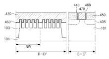
도 8을 참조하면, 기판은 N형 불순물로 도핑된 영역인 N웰(well) 영역(NW) 및 그 외 P형 불순물로 도핑된 영역을 포함할 수 있다. 제1 활성 패턴들(10, 20) 중 일부(10)는 N웰 영역(NW)에 형성되고, 나머지(20)는 P형 불순물로 도핑된 영역에 형성될 수 있다. 제2 활성 패턴들(15) 중에서도 일부는 N웰 영역(NW)에 형성되고, 나머지는 P형 불순물로 도핑된 영역에 형성될 수 있다. 도 8에 대한 설명의 편의를 위해, N웰 영역(NW)에 형성된 제1 활성 패턴들(10)은 제1 활성 핀들(10)로 다시 명명하고, P형 불순물로 도핑된 영역에 형성된 제1 활성 패턴들(20)은 제2 활성 핀들(20)로 다시 명명한다. 또한, 제2 활성 패턴들(15)는 제3 활성 핀들(15)로 다시 명명한다.Referring to FIG. 8 , the substrate may include an N well region NW, which is a region doped with an N-type impurity, and other regions doped with a P-type impurity. A
서로 이격된 제1 활성 핀들(10), 제2 활성 핀들(20) 및 제3 활성 핀들(15)은 일 방향(예를 들어, y 방향)으로 길게 연장되도록 형성될 수 있다. 게이트 전극들(621, 625)은 타 방향(예를 들어, x 방향)으로 연장되도록 형성될 수 있다. 게이트 전극들(621, 625)은 제1 내지 제3 활성 핀들(10, 15, 20) 모두와 교차하도록 연장될 수 있다.The first
도시하지 않았으나, 게이트 전극들(621, 625)과 활성 핀들(10, 15, 20)이 교차되는 영역에서 각 게이트 전극의 양측에 위치한 활성 핀들에 소스/드레인 영역들이 형성될 수 있다.Although not shown, source/drain regions may be formed in the active fins positioned on both sides of each gate electrode in a region where the
또한, 상기 소스/드레인 영역들에 연결되는 소스/드레인 컨택들(640)이 형성될 수 있다. 각각의 게이트 전극에 연결되는 입력 단자들(643, 645) 및 출력 단자(647)이 형성될 수 있다.In addition, source/
제1 활성 핀들(10)은 PMOS 트랜지스터를 구성하고, 제2 활성 핀들(20)은 NMOS 트랜지스터를 구성할 수 있다. 구체적으로, 제1 활성 핀들(10) 상에 2개의 게이트 전극들(621, 625) 및 3개의 소스/드레인 컨택들(640)이 배치되므로, 제1 활성 핀들(10)은 병렬 연결된 2개의 PMOS 트랜지스터들을 구성할 수 있다. 또한, 제2 활성 핀들(20)의 상에는 2개의 게이트 전극들(621, 625) 및 2 개의 소스/드레인 컨택들(640)이 배치되므로, 제2 활성 핀들(20)은 직렬 연결된 2 개의 NMOS 트랜지스터들을 구성할 수 있다.
The first
도 9a 내지 도 9f는 본 발명의 일 실시예에 따른 반도체 소자의 제조 방법을 설명하기 위한 단면도들이다. 도 9a 내지 도 9f에는 도 8의 절단선 D-D'에 대응하는 부분 및 절단선 E-E'에 대응하는 부분이 도시된다. 도 9a 내지 도 9f는 도 2j에 도시된 구조를 기초로 하여 본 발명의 일 실시예에 따른 반도체 소자(1)를 제조하기 위한 후속의 공정들을 개략적으로 나타내는 도면들이다.
9A to 9F are cross-sectional views illustrating a method of manufacturing a semiconductor device according to an embodiment of the present invention. 9A to 9F show a portion corresponding to the cutting line D-D' of FIG. 8 and a portion corresponding to the cutting line E-E' of FIG. 8 . 9A to 9F are diagrams schematically illustrating subsequent processes for manufacturing the
도 9a는 도 2a 내지 도 2j를 참조하여 설명한 공정들이 수행된 결과를 나타내는 것이다. 도 9a를 참조하면, 기판(101)은 N웰 영역(NW)을 포함할 수 있다. N웰 영역(NW) 외의 영역들은 P형 불순물로 도핑된 영역들일 수 있다. 상기 N웰 영역(NW)은 활성 패턴들(10, 15, 20)을 형성하기 전에 기판(101)에 미리 형성될 수 있다.
9A shows the results of the processes described with reference to FIGS. 2A to 2J. Referring to FIG. 9A , the
도 9b를 참조하면, 소자 분리층(103) 상으로 노출된 활성 패턴들(10, 15, 20)을 덮는 희생 게이트 절연층(410) 및 희생 게이트 전극(420)을 형성할 수 있다.Referring to FIG. 9B , a sacrificial
먼저, 희생 게이트 절연층(410), 희생 게이트 전극(420) 및 마스크층(430)을 순차적으로 형성할 수 있다. 이어서, 마스크층(430)을 패터닝한 후, 이를 식각 마스크로 이용하여 희생 게이트 전극(420)을 패터닝할 수 있다.First, the sacrificial
희생 게이트 절연층(410)은 실리콘 산화막 또는 실리콘 산질화막 중에서 적어도 하나를 포함할 수 있으나, 이에 한정되는 것은 아니다. 희생 게이트 전극층(420)은 다결정질 실리콘으로 이루어질 수 있으나, 이에 한정되는 것은 아니다.
The sacrificial
도 9c를 참조하면, 희생 게이트 전극(430)의 측면에 게이트 스페이서(440)를 형성하고, 희생 게이트 전극(430)의 측면에 노출된 활성 패턴 내에 소스/드레인 영역(435)을 형성할 수 있다.Referring to FIG. 9C , a
먼저, 스페이서 물질층을 희생 게이트 전극(430) 상에 콘포멀하게 형성한 후, 스페이서 물질층을 에치백함으로써, 게이트 스페이서(440)을 형성할 수 있다. 이어서, 불순물을 이온 주입함으로써, 소스/드레인 영역(435)을 형성할 수 있다. 불순물들의 활성화를 위해, 이온 주입 후 열처리 공정이 수행될 수 있다.
First, a spacer material layer is conformally formed on the
도 9d를 참조하면, 희생 게이트 전극(420) 및 게이트 스페이서(440)을 둘러싸고, 희생 게이트 전극(420)의 상면을 노출시키는 층간 절연층(450)을 형성할 수 있다.Referring to FIG. 9D , an
먼저, 희생 게이트 전극(420) 및 게이트 스페이서(440)을 덮는 층간 절연층(450)을 형성한 후, 이어서 희생 게이트 전극(420)의 상면이 노출되도록 평탄화 공정을 수행할 수 있다. 평탄화 공정을 통해, 층간 절연층(450)이 완성될 수 있다.First, after forming the interlayer insulating
상기 층간 절연층(450)을 평탄화하는 공정은 화학적 기계적 연마(Chemical Mechanical Polishing) 공정일 수 있다.
The process of planarizing the interlayer insulating
도 9e 및 9f를 참조하면, 게이트 절연층(460) 및 게이트 전극(470)을 형성할 수 있다.9E and 9F , a
먼저, 희생 게이트 전극(420) 및 희생 게이트 절연층(410)을 제거하여, 층간 절연층(450) 내에 트렌치를 형성할 수 있다. 다음으로, 상기 트렌치 내에 게이트 절연층(460) 및 게이트 전극(470)을 콘포멀하게 형성할 수 있다. 이어서, 층간 절연층(450)의 상면이 노출되도록 평탄화 공정을 수행할 수 있다. 평탄화 공정을 통해, 게이트 전극(470)이 완성될 수 있다.First, a trench may be formed in the
게이트 절연층(460)은 고유전막으로 형성될 수 있다. 상기 고유전막은 실리콘 산화막보다 높은 유전 상수를 가지는 절연성 물질들을 의미하며, 탄탈륨 산화막, 티타늄 산화막, 하프늄 산화막, 지르코늄 산화막, 알루미늄 산화막, 이트륨 산화막, 니오븀 산화막, 하프늄 실리케이트, 지르코늄 실리케이트 중 적어도 하나일 수 있다. 게이트 절연층(460)은 화학 기상 증착법(CVD) 또는 원자층 증착법(ALD)에 의해 형성될 수 있다.The
게이트 전극(470)은 적어도 하나의 일함수 조절막 및 적어도 하나의 게이트 금속을 포함할 수 있다. 상기 일함수 조절막은 TiN, TaN, WN, TiAl, TiAlN, TaC 또는 TiC 등으로 이루어진 그룹에서 선택된 어느 하나일 수 있다. 상기 게이트 금속은 알루미늄(Al), 텅스텐(W), 또는 몰리브데늄(Mo) 등 중의 적어도 하나일 수 있다. 상기 일함수 조절막은 상기 게이트 금속에 대한 확산 방지막으로서 역할을 할 수도 있다. 게이트 전극(470)는 그 물질에 따라 화학 기상 증착법 또는 원자층 증착법에 의해 형성될 수 있다.The
N웰 영역(NW)에서의 상기 일함수 조절막은 그외 영역(P형 불순물로 도핑된 영역)에서의 상기 일함수 조절막과 서로 다를 수 있고, 이를 구현하기 위해, 추가적인 공정이 필요할 수 있다.
The work function control layer in the N well region NW may be different from the work function control layer in other regions (regions doped with a P-type impurity), and an additional process may be required to implement this.
도 10 및 도 11은 본 발명의 일 실시예에 따른 반도체 소자를 설명하기 위한 회로도 및 레이아웃도이다.10 and 11 are circuit diagrams and layout diagrams for explaining a semiconductor device according to an embodiment of the present invention.
구체적으로, 도 10 및 도 11에 도시된 반도체 소자(2)는 6개의 트랜지스터로 구성되는 정적 랜덤 액세스 메모리(SRAM)의 셀에 대한 것이다. 이는 예시적인 것이며, 본 발명은 이에 한정되지 않는다.
Specifically, the
도 10을 참조하면, SRAM 셀은 전원 노드(Vcc)와 접지 노드(Vss) 사이에 병렬 연결된 한 쌍의 인버터(INV1, INV2)와, 각각의 인버터(INV1, INV2)의 출력 노드에 연결된 제1 패스 트랜지스터(PS1) 및 제2 패스 트랜지스터(PS2)를 포함할 수 있다. 제1 패스 트랜지스터(PS1)와 제2 패스 트랜지스터(PS2)는 각각 비트 라인(BL)과 상보 비트 라인(BL/)과 연결될 수 있다. 제1 패스 트랜지스터(PS1)와 제2 패스 트랜지스터(PS2)의 게이트는 워드 라인(WL)과 연결될 수 있다.Referring to FIG. 10 , the SRAM cell includes a pair of inverters INV1 and INV2 connected in parallel between a power node Vcc and a ground node Vss, and a first connected to an output node of each of the inverters INV1 and INV2. It may include a pass transistor PS1 and a second pass transistor PS2. The first pass transistor PS1 and the second pass transistor PS2 may be respectively connected to the bit line BL and the complementary bit line BL/. Gates of the first pass transistor PS1 and the second pass transistor PS2 may be connected to the word line WL.
제1 인버터(INV1)는 직렬로 연결된 제1 풀업 트랜지스터(PU1)와 제1 풀다운 트랜지스터(PD1)를 포함하고, 제2 인버터(INV2)는 직렬로 연결된 제2 풀업 트랜지스터(PU2)와 제2 풀다운 트랜지스터(PD2)를 포함한다. 제1 풀업 트랜지스터(PU1)와 제2 풀업 트랜지스터(PU2)은 PMOS 트랜지스터이고, 제1 풀다운 트랜지스터(PD1)와 제2 풀다운 트랜지스터(PD2)는 NMOS 트랜지스터일 수 있다.The first inverter INV1 includes a first pull-up transistor PU1 and a first pull-down transistor PD1 connected in series, and the second inverter INV2 includes a second pull-up transistor PU2 and a second pull-down transistor PU2 connected in series. and a transistor PD2. The first pull-up transistor PU1 and the second pull-up transistor PU2 may be PMOS transistors, and the first pull-down transistor PD1 and the second pull-down transistor PD2 may be NMOS transistors.
또한, 제1 인버터(INV1) 및 제2 인버터(INV2)는 하나의 래치회로(latch circuit)를 구성하기 위하여 제1 인버터(INV1)의 입력 노드가 제2 인버터(INV2)의 출력 노드와 연결되고, 제2 인버터(INV2)의 입력 노드는 제1 인버터(INV1)의 출력 노드와 연결된다.
In addition, in the first inverter INV1 and the second inverter INV2, the input node of the first inverter INV1 is connected to the output node of the second inverter INV2 to form one latch circuit, and , an input node of the second inverter INV2 is connected to an output node of the first inverter INV1 .
도 11을 참조하면, 기판은 N형 불순물로 도핑된 영역인 N웰(well) 영역(NW) 및 그 외 P형 불순물로 도핑된 영역을 포함할 수 있다. 제1 피치(P1)를 가지는 제1 활성 패턴들(30, 40)은 P형 불순물로 도핑된 영역에 형성되고, 제2 피치(P2)를 가지는 제2 활성 패턴들(35)는 N웰 영역(NW)에 형성될 수 있다. 도 11에 대한 설명의 편의를 위해, P형 불순물로 도핑된 영역에 형성된 일부 제1 활성 패턴들(30)을 제1 활성 핀들(30)로, 나머지 제1 활성 패턴들(40)을 제4 활성 핀들(40)으로 다시 명명한다. 또한, N웰 영역(NW)에 형성된 일부 제2 활성 패턴(35a)은 제2 활성 핀(35a)로 다시 명명하고, 나머지 제2 활성 패턴(35b)은 제3 활성 핀(35b)로 다시 명명한다.Referring to FIG. 11 , the substrate may include an N well region NW, which is a region doped with an N-type impurity, and other regions doped with a P-type impurity. The first
서로 이격된 제1 활성 핀들(30), 제2 활성 핀(35a), 제3 활성 핀(35b), 제4 활성 핀들(40)은 일 방향(예를 들어, y 방향)으로 길게 연장되도록 형성될 수 있다. 제2 활성 핀(35a)과 제3 활성 핀(35b)은 제1 활성 핀들(30)과 제4 활성 핀들(40)보다 연장된 길이가 짧을 수 있다. 제2 및 제3 활성 핀(35a, 35b)은 PMOS 트랜지스터를 구성하고, 제1 및 제4 활성 핀들(30, 40)은 NMOS 트랜지스터를 구성할 수 있다.The first
또한, 제1 게이트 전극(651), 제2 게이트 전극(653), 제3 게이트 전극(655), 제4 게이트 전극(657)은 타 방향(예를 들어, x 방향)으로 길게 연장되고, 제1 활성 핀들(30) 내지 제4 활성 핀들(40)을 교차하도록 형성될 수 있다. 구체적으로, 제1 게이트 전극(651)은 제1 활성 핀들(30)과 제2 활성 핀들(35a)을 완전히 교차하고, 제3 활성 핀(35b)의 종단과 일부 오버랩될 수 있다. 제3 게이트 전극(655)은 제4 활성 핀들(40)과 제3 활성 핀(35b)을 완전히 교차하고, 제2 활성 핀(35a)의 종단과 일부 오버랩될 수 있다. 제2 게이트 전극(653)과 제4 게이트 전극(657)은 각각 제1 활성 핀들(30)과 제4 활성 핀들(40)을 교차하도록 형성될 수 있다.In addition, the
도시된 것과 같이, 제1 풀업 트랜지스터(PU1)는 제1 게이트 전극(651)과 제2 활성 핀(35a)이 교차되는 영역에 정의되고, 제1 풀다운 트랜지스터(PD1)는 제1 게이트 전극(651)과 제1 활성 핀들(30)이 교차되는 영역에 정의되고, 제1 패스 트랜지스터(PS1)는 제2 게이트 전극(653)과 제1 활성 핀들(30)이 교차되는 영역에 정의될 수 있다. 제2 풀업 트랜지스터(PU2)는 제3 게이트 전극(653)과 제3 활성 핀(35b)이 교차되는 영역에 정의되고, 제2 풀다운 트랜지스터(PD2)는 제3 게이트 전극(655)과 제4 활성 핀들(40)이 교차되는 영역에 정의되고, 제2 패스 트랜지스터(PS2)는 제4 게이트 전극(657)과 제4 활성 핀들(40)이 교차되는 영역에 정의될 수 있다.As shown, the first pull-up transistor PU1 is defined in a region where the
도시하지 않았으나, 제1 내지 제4 게이트 전극(651, 653, 655, 657)과 제1 내지 제4 활성 핀들(30, 35a, 35b, 40)이 교차되는 영역에서 각 게이트 전극의 양측의 활성 핀들에는 소스/드레인 영역들이 형성될 수 있다.Although not shown, in a region where the first to
또한, 상기 각각의 소스/드레인 영역에 연결되는 복수의 소스/드레인 컨택들(670)이 형성될 수 있다.In addition, a plurality of source/
뿐만 아니라, 제1 공유 컨택(shared contact)(675a)은 제2 활성 핀(35a), 제3 게이트 라인(655)과, 배선(677)을 동시에 연결할 수 있다. 제2 공유 컨택(675b)은 제3 활성 핀(35b), 제1 게이트 라인(651)과, 배선(678)을 동시에 연결할 수 있다.
In addition, the first shared contact 675a may simultaneously connect the second
도 12a 내지 도 12f는 본 발명의 일 실시예에 따른 반도체 소자의 제조 방법을 설명하기 위한 단면도들이다. 도 12a 내지 도 12f에는 도 11의 절단선 F-F'에 대응하는 부분 및 절단선 G-G'에 대응하는 부분이 도시된다. 도 12a 내지 도 12f는 도 4j에 도시된 구조를 기초로 하여 본 발명의 일 실시예에 따른 반도체 소자(2)를 제조하기 위한 후속의 공정들을 개략적으로 나타내는 도면들이다.
12A to 12F are cross-sectional views illustrating a method of manufacturing a semiconductor device according to an exemplary embodiment. 12A to 12F show a portion corresponding to the cutting line F-F' of FIG. 11 and a portion corresponding to the cutting line G-G' of FIG. 11 . 12A to 12F are diagrams schematically illustrating subsequent processes for manufacturing the
도 12a는 도 4a 내지 도 4j를 참조하여 설명한 공정들이 수행된 결과를 나타내는 것이다. 도 12a를 참조하면, 기판(201)은 N웰 영역(NW)을 포함할 수 있다. N웰 영역(NW) 외의 영역들은 P형 불순물로 도핑된 영역들일 수 있다. 상기 N웰 영역(NW)은 활성 패턴들(30, 35, 40)을 형성하기 전에 기판(201)에 미리 형성될 수 있다.
12A shows the results of the processes described with reference to FIGS. 4A to 4J. Referring to FIG. 12A , the
도 12b를 참조하면, 소자 분리층(203) 상으로 노출된 활성 패턴들(30, 35, 40)을 덮는 희생 게이트 절연층(510) 및 희생 게이트 전극(520)을 형성할 수 있다.Referring to FIG. 12B , a sacrificial
먼저, 희생 게이트 절연층(510), 희생 게이트 전극(520) 및 마스크층(530)을 순차적으로 형성할 수 있다. 이어서, 마스크층(530)을 패터닝한 후, 이를 식각 마스크로 이용하여 희생 게이트 전극(520)을 패터닝할 수 있다.First, the sacrificial
희생 게이트 절연층(510)은 실리콘 산화막 또는 실리콘 산질화막 중에서 적어도 하나를 포함할 수 있으나, 이에 한정되는 것은 아니다. 희생 게이트 전극층(520)은 다결정질 실리콘으로 이루어질 수 있으나, 이에 한정되는 것은 아니다.
The sacrificial
도 12c를 참조하면, 희생 게이트 전극(530)의 측면에 게이트 스페이서(540)를 형성하고, 희생 게이트 전극(530)의 측면에 노출된 활성 패턴 내에 소스/드레인 영역(535)을 형성할 수 있다.Referring to FIG. 12C , a
먼저, 스페이서 물질층을 희생 게이트 전극(530) 상에 콘포멀하게 형성한 후, 스페이서 물질층을 에치백함으로써, 게이트 스페이서(540)을 형성할 수 있다. 이어서, 불순물을 이온 주입함으로써, 소스/드레인 영역(535)을 형성할 수 있다. 불순물들의 활성화를 위해, 이온 주입 후 열처리 공정이 수행될 수 있다.
First, a spacer material layer is conformally formed on the
도 12d를 참조하면, 희생 게이트 전극(520) 및 게이트 스페이서(540)을 둘러싸고, 희생 게이트 전극(520)의 상면을 노출시키는 층간 절연층(550)을 형성할 수 있다.Referring to FIG. 12D , an
먼저, 희생 게이트 전극(520) 및 게이트 스페이서(540)을 덮는 층간 절연층(550)을 형성한 후, 이어서 희생 게이트 전극(520)의 상면이 노출되도록 평탄화 공정을 수행할 수 있다. 평탄화 공정을 통해, 층간 절연층(550)이 완성될 수 있다.First, after forming the interlayer insulating
상기 층간 절연층(550)을 평탄화하는 공정은 화학적 기계적 연마(Chemical Mechanical Polishing) 공정일 수 있다.
The process of planarizing the interlayer insulating
도 12e 및 12f를 참조하면, 게이트 절연층(560) 및 게이트 전극(570)을 형성할 수 있다.12E and 12F , a
먼저, 희생 게이트 전극(520) 및 희생 게이트 절연층(510)을 제거하여, 층간 절연층(550) 내에 트렌치를 형성할 수 있다. 상기 트렌치 내에 게이트 절연층(560) 및 게이트 전극(570)을 콘포멀하게 형성할 수 있다. 이어서, 층간 절연층(550)의 상면이 노출되도록 평탄화 공정을 수행할 수 있다. 평탄화 공정을 통해, 게이트 전극(570)이 완성될 수 있다.First, a trench may be formed in the
게이트 절연층(560)은 고유전막을 포함할 수 있다. 상기 고유전막은 실리콘 산화막보다 큰 유전율을 가지는 절연성 물질들을 의미하며, 탄탈륨 산화막, 티타늄 산화막, 하프늄 산화막, 지르코늄 산화막, 알루미늄 산화막, 이트륨 산화막, 니오븀 산화막, 하프늄 실리케이트, 지르코늄 실리케이트 중 적어도 하나일 수 있다. 게이트 절연층(560)은 화학 기상 증착법(CVD) 또는 원자층 증착법(ALD)에 의해 형성될 수 있다.The
게이트 전극(570)은 적어도 하나의 일함수 조절막 및 적어도 하나의 게이트 금속을 포함할 수 있다. 상기 일함수 조절막은 TiN, TaN, WN, TiAl, TiAlN, TaC 또는 TiC 등으로 이루어진 그룹에서 선택된 어느 하나일 수 있다. 상기 게이트 금속은 알루미늄(Al), 텅스텐(W), 또는 몰리브데늄(Mo) 등 중의 적어도 하나일 수 있다. 상기 일함수 조절막은 상기 게이트 금속에 대한 확산 방지막으로서 역할을 할 수도 있다. 게이트 전극(570)는 그 물질에 따라 화학 기상 증착법 또는 원자층 증착법에 의해 형성될 수 있다.The
N웰 영역(NW)에서의 상기 일함수 조절막은 그외 영역(P형 불순물로 도핑된 영역)에서의 상기 일함수 조절막과 서로 다를 수 있고, 이를 구현하기 위해, 추가적인 공정이 필요할 수 있다.
The work function control layer in the N well region NW may be different from the work function control layer in other regions (regions doped with a P-type impurity), and an additional process may be required to implement this.
도 14를 본 발명의 일 실시예에 따른 반도체 장치를 포함하는 저장 장치를 나타낸 블록도이다.14 is a block diagram illustrating a storage device including a semiconductor device according to an embodiment of the present invention.
도 14를 참조하면, 본 실시예에 따른 저장 장치(1000)는 호스트(HOST)와 통신하는 컨트롤러(1010) 및 데이터를 저장하는 메모리(1020-1, 1020-2, 1020-3)를 포함할 수 있다. 컨트롤러(1010) 및 각 메모리(1020-1, 1020-2, 1020-3)는, 상술한 본 발명의 일 실시예에 따른 반도체 소자를 포함할 수 있다.Referring to FIG. 14 , the
컨트롤러(1010)와 통신하는 호스트(HOST)는 저장 장치(1000)가 장착되는 다양한 전자 기기일 수 있으며, 예를 들어 스마트폰, 디지털 카메라, 데스크 톱, 랩톱, 미디어 플레이어 등일 수 있다. 컨트롤러(1010)는 호스트(HOST)에서 전달되는 데이터 쓰기 또는 읽기 요청을 수신하여 메모리(1020-1, 1020-2, 1020-3)에 데이터를 저장하거나, 메모리(1020-1, 1020-2, 1020-3)로부터 데이터를 인출하기 위한 명령(CMD)을 생성할 수 있다.The host (HOST) communicating with the
도 14에 도시한 바와 같이, 저장 장치(1000) 내에 하나 이상의 메모리(1020-1, 1020-2, 1020-3)가 컨트롤러(1010)에 병렬로 연결될 수 있다. 복수의 메모리(1020-1, 1020-2, 1020-3)를 컨트롤러(1010)에 병렬로 연결함으로써, SSD(Solid State Drive)와 같이 큰 용량을 가지는 저장 장치(1000)를 구현할 수 있다.
14 , one or more memories 1020-1, 1020-2, and 1020-3 in the
도 15를 본 발명의 일 실시예에 따른 반도체 장치를 포함하는 전자 기기를 나타낸 블록도이다.15 is a block diagram illustrating an electronic device including a semiconductor device according to an embodiment of the present invention.
도 15를 참조하면, 본 실시예에 따른 전자 기기(2000)는 통신부(2010), 입력부(2020), 출력부(2030), 메모리(2040) 및 프로세서(2050)를 포함할 수 있다.Referring to FIG. 15 , the
통신부(2010)는 유/무선 통신 모듈을 포함할 수 있으며, 무선 인터넷 모듈, 근거리 통신 모듈, GPS 모듈, 이동통신 모듈 등을 포함할 수 있다. 통신부(2010)에 포함되는 유/무선 통신 모듈은 다양한 통신 표준 규격에 의해 외부 통신망과 연결되어 데이터를 송수신할 수 있다.The
입력부(2020)는 사용자가 전자 기기(2000)의 동작을 제어하기 위해 제공되는 모듈로서, 기계식 스위치, 터치스크린, 음성 인식 모듈 등을 포함할 수 있다. 또한, 입력부(2020)는 트랙 볼 또는 레이저 포인터 방식 등으로 동작하는 마우스, 또는 핑거 마우스 장치를 포함할 수도 있으며, 그 외에 사용자가 데이터를 입력할 수 있는 다양한 센서 모듈을 더 포함할 수도 있다.The
출력부(2030)는 전자 기기(2000)에서 처리되는 정보를 음성 또는 영상의 형태로 출력하며, 메모리(2040)는 프로세서(2050)의 처리 및 제어를 위한 프로그램이나, 또는 데이터 등을 저장할 수 있다. 프로세서(2050)는 필요한 동작에 따라 메모리(2040)에 명령어를 전달하여 데이터를 저장 또는 인출할 수 있다. 프로세서(2050) 및 메모리(2040)는 상술한 본 발명의 일 실시예에 따른 반도체 소자를 포함할 수 있다.The
메모리(2040)는 전자 기기(2000)에 내장되거나 또는 별도의 인터페이스를 통해 프로세서(2050)와 통신할 수 있다. 별도의 인터페이스를 통해 프로세서(2050)와 통신하는 경우, 프로세서(2050)는 SD, SDHC, SDXC, MICRO SD, USB 등과 같은 다양한 인터페이스 규격을 통해 메모리(2040)에 데이터를 저장하거나 또는 인출할 수 있다.The
프로세서(2050)는 전자 기기(2000)에 포함되는 각부의 동작을 제어한다. 프로세서(2050)는 음성 통화, 화상 통화, 데이터 통신 등과 관련된 제어 및 처리를 수행하거나, 멀티미디어 재생 및 관리를 위한 제어 및 처리를 수행할 수도 있다. 또한, 프로세서(2050)는 입력부(2020)를 통해 사용자로부터 전달되는 입력을 처리하고 그 결과를 출력부(2030)를 통해 출력할 수 있다. 또한, 프로세서(2050)는 앞서 설명한 바와 같이 전자 기기(2000)의 동작을 제어하는데 있어서 필요한 데이터를 메모리(2040)에 저장하거나 메모리(2040)로부터 인출할 수 있다.
The
도 16은 본 발명의 일 실시예에 따른 반도체 장치를 포함하는 시스템을 보여주는 개략도이다.16 is a schematic diagram illustrating a system including a semiconductor device according to an embodiment of the present invention.
도 16을 참조하면, 시스템(3000)은 제어기(3100), 입/출력 장치(3200), 메모리(3300) 및 인터페이스(3400)를 포함할 수 있다. 시스템(3000)은 모바일 시스템 또는 정보를 전송하거나 전송받는 시스템일 수 있다. 상기 모바일 시스템은 PDA, 휴대용 컴퓨터(portable computer), 웹 타블렛(web tablet), 무선 폰(wireless phone), 모바일 폰(mobile phone), 디지털 뮤직 플레이어(digital music player) 또는 메모리 카드(memory card)일 수 있다.Referring to FIG. 16 , a
제어기(3100)는 프로그램을 실행하고, 시스템(3000)을 제어하는 역할을 할 수 있다. 제어기(3100)는, 예를 들어 마이크로프로세서(microprocessor), 디지털 신호 처리기(digital signal processor), 마이크로콘트롤러(microcontroller) 또는 이와 유사한 장치일 수 있다.The
입/출력 장치(3200)는 시스템(3000)의 데이터를 입력 또는 출력하는데 이용될 수 있다. 시스템(3000)은 입/출력 장치(3200)를 이용하여 외부 장치, 예컨대 개인용 컴퓨터 또는 네트워크에 연결되어, 외부 장치와 서로 데이터를 교환할 수 있다. 입/출력 장치(3200)는, 예를 들어 키패드(keypad), 키보드(keyboard) 또는 표시장치(display)일 수 있다.The input/
메모리(3300)는 제어기(3100)의 동작을 위한 코드 및/또는 데이터를 저장하거나, 및/또는 제어기(3100)에서 처리된 데이터를 저장할 수 있다.The
인터페이스(3400)는 시스템(3000)과 외부의 다른 장치 사이의 데이터 전송통로일 수 있다. 제어기(3100), 입/출력 장치(3200), 메모리(3300) 및 인터페이스(3400)는 버스(3500)를 통하여 서로 통신할 수 있다.The
제어기(3100) 또는 메모리(3300) 중 적어도 하나는 상술한 본 발명의 일 실시예에 따른 반도체 소자를 포함할 수 있다.
At least one of the
본 발명은 상술한 실시예 및 첨부된 도면에 의해 한정되는 것이 아니며 첨부된 청구범위에 의해 한정하고자 한다. 따라서, 청구범위에 기재된 본 발명의 기술적 사상을 벗어나지 않는 범위 내에서 당 기술분야의 통상의 지식을 가진 자에 의해 다양한 형태의 치환, 변형 및 변경이 가능할 것이며, 이 또한 본 발명의 범위에 속한다고 할 것이다.
The present invention is not limited by the above-described embodiments and the accompanying drawings, but is intended to be limited by the appended claims. Therefore, various types of substitution, modification and change will be possible by those skilled in the art within the scope not departing from the technical spirit of the present invention described in the claims, and it is also said that it falls within the scope of the present invention. something to do.
101: 기판103: 소자 분리층
105: 제1 하드 마스크층110: 제2 하드 마스크층
115: 제3 하드 마스크층121: 제1 희생층
125: 제1 반사방지층120a, 120d: 제2 및 제3 맨드럴
141: 제2 희생층145: 제2 반사방지층
140: 제1 맨드럴 150s: 제1 스페이서
160a, 160d: 제2 및 제3 스페이서
190p: 제1 감광막 패턴
10, 20: 제1 활성 패턴15: 제2 활성 패턴101: substrate 103: device isolation layer
105: first hard mask layer 110: second hard mask layer
115: third hard mask layer 121: first sacrificial layer
125: first
141: second sacrificial layer 145: second anti-reflection layer
140:
160a, 160d: second and third spacers
190p: first photoresist pattern
10, 20: first active pattern 15: second active pattern
Claims (20)
Translated fromKorean상기 제2 희생층을 식각함으로써 상기 제1 희생층 상에 제1 맨드럴(mandrel)들을 형성하는 단계;
상기 제1 맨드럴들의 측벽에 제1 스페이서들을 형성하는 단계;
상기 제1 맨드럴들을 제거한 영역 밖에 위치하며, 상기 제1 스페이서들로부터 이격되고, 상기 제1 스페이서들의 선폭보다 넓은 선폭을 가지는 감광막 패턴을 형성하는 단계;
상기 제1 스페이서들 및 상기 감광막 패턴을 식각 마스크로 이용하여 상기 제1 희생층을 식각함으로써 제2 및 제3 맨드럴을 형성하는 단계;
상기 제2 및 제3 맨드럴의 측벽에 제2 및 제3 스페이서들을 형성하는 단계;
상기 제2 및 제3 스페이서들을 이용하여 상기 하드 마스크층 및 상기 기판의 적어도 일부를 식각함으로써, 제1 피치를 가지는 제1 활성 패턴 및 상기 제1 피치보다 넓은 제2 피치를 가지는 제2 활성 패턴들을 형성하는 단계; 및
상기 제1 및 제2 활성 패턴들의 상부가 돌출되도록 소자 분리층을 형성하는 단계;를 포함하는 반도체 소자의 제조 방법.
sequentially stacking hard mask layers, a first sacrificial layer, and a second sacrificial layer on a substrate;
forming first mandrels on the first sacrificial layer by etching the second sacrificial layer;
forming first spacers on sidewalls of the first mandrels;
forming a photoresist pattern located outside the region from which the first mandrels are removed, spaced apart from the first spacers, and having a line width wider than the line width of the first spacers;
forming second and third mandrels by etching the first sacrificial layer using the first spacers and the photoresist pattern as an etch mask;
forming second and third spacers on sidewalls of the second and third mandrels;
By etching at least a portion of the hard mask layer and the substrate using the second and third spacers, a first active pattern having a first pitch and a second active pattern having a second pitch wider than the first pitch are formed. forming; and
and forming a device isolation layer so that upper portions of the first and second active patterns protrude.
상기 제1 피치는 30nm 내지 35nm의 범위를 가지고, 상기 제2 피치는 40nm 내지 50nm의 범위를 가지는 것을 특징으로 하는 반도체 소자의 제조 방법.
According to claim 1,
The first pitch has a range of 30nm to 35nm, the second pitch is a method of manufacturing a semiconductor device, characterized in that it has a range of 40nm to 50nm.
상기 제2 및 제3 스페이서들을 형성하는 단계 후에, 상기 제2 및 제3 맨드럴을 제거하는 단계를 더 포함하고,
상기 제2 및 제3 맨드럴을 제거함으로써, 서로 다른 피치를 가지는 라인형태로 잔존하는 제2 및 제3 스페이서들을 마련하고,
상기 제2 스페이서들의 피치는 상기 제1 스페이서들의 선폭에 의해 결정되고, 상기 제3 스페이서들의 피치는 상기 감광막 패턴의 선폭에 의해 결정되는 것을 특징으로 하는 반도체 소자의 제조 방법.
According to claim 1,
after forming the second and third spacers, further comprising removing the second and third mandrels;
By removing the second and third mandrels, second and third spacers remaining in the form of lines having different pitches are provided;
A pitch of the second spacers is determined by line widths of the first spacers, and a pitch of the third spacers is determined by a line width of the photoresist pattern.
상기 제3 스페이서들의 피치는 상기 제2 스페이서들의 피치보다 넓은 것을 특징으로 하는 반도체 소자의 제조 방법.
According to claim 1,
The method of manufacturing a semiconductor device, characterized in that the pitch of the third spacers is wider than the pitch of the second spacers.
상기 제2 희생층 상에 형성된 제1 감광막 패턴을 식각 마스크로 이용하여 상기 제2 희생층을 식각함으로써 제1 맨드럴을 형성하는 단계;
상기 제1 맨드럴의 측벽에 제1 스페이서들을 형성하는 단계;
상기 제1 맨드럴을 제거한 영역 내에 위치하며, 상기 제1 스페이서들로부터 이격되고, 제1 스페이서들의 선폭보다 넓은 선폭을 가지는 제2 감광막 패턴을 형성하는 단계;
상기 제1 스페이서들 및 제2 감광막 패턴을 식각 마스크로 이용하여 제1 희생층을 식각함으로써 각각 서로 다른 선폭을 가지는 제2 및 제3 맨드럴을 형성하는 단계;
상기 제2 및 제3 맨드럴의 측벽에 각각 제2 및 제3 스페이서들을 형성하는 단계;
서로 다른 피치를 가지는 상기 제2 및 제3 스페이서들을 식각 마스크로 이용하여 하드 마스크층들을 식각함으로써 하드 마스크 패턴을 형성하는 단계;
상기 하드 마스크 패턴을 식각 마스크로 이용하여 기판을 식각함으로써 제1 피치를 가지는 제1 활성 패턴 및 상기 제1 피치보다 넓은 제2 피치를 가지는 제2 활성 패턴들을 형성하는 단계; 및
상기 제1 및 제2 활성 패턴들의 상부가 돌출되도록 소자 분리층을 형성하는 단계;를 포함하는 반도체 소자의 제조 방법.
sequentially stacking hard mask layers, a first sacrificial layer, and a second sacrificial layer on a substrate;
forming a first mandrel by etching the second sacrificial layer using the first photoresist pattern formed on the second sacrificial layer as an etch mask;
forming first spacers on sidewalls of the first mandrel;
forming a second photoresist layer pattern located in the region from which the first mandrel is removed, spaced apart from the first spacers, and having a line width wider than the line width of the first spacers;
forming second and third mandrels having different line widths by etching the first sacrificial layer using the first spacers and the second photoresist pattern as an etch mask;
forming second and third spacers on sidewalls of the second and third mandrels, respectively;
forming a hard mask pattern by etching hard mask layers using the second and third spacers having different pitches as etch masks;
etching the substrate using the hard mask pattern as an etch mask to form first active patterns having a first pitch and second active patterns having a second pitch wider than the first pitch; and
and forming a device isolation layer so that upper portions of the first and second active patterns protrude.
상기 제1 피치는 30nm 내지 35nm의 범위를 가지고, 상기 제2 피치는 40nm 내지 50nm의 범위를 가지는 것을 특징으로 하는 반도체 소자의 제조 방법.
6. The method of claim 5,
The first pitch has a range of 30nm to 35nm, the second pitch is a method of manufacturing a semiconductor device, characterized in that it has a range of 40nm to 50nm.
상기 제3 맨드럴의 선폭은 상기 제2 맨드럴의 선폭보다 넓은 것을 특징으로 하는 반도체 소자의 제조 방법.
6. The method of claim 5,
The method of manufacturing a semiconductor device, characterized in that the line width of the third mandrel is wider than the line width of the second mandrel.
상기 제2 및 제3 스페이서들을 형성하는 단계 후에, 상기 제2 및 제3 맨드럴을 제거하는 단계를 더 포함하고,
상기 제2 및 제3 맨드럴을 제거함으로써, 서로 다른 피치를 가지는 라인형태로 잔존하는 제2 및 제3 스페이서들을 마련하고,
상기 제2 스페이서들의 피치는 상기 제1 스페이서들의 선폭에 의해 결정되고, 상기 제3 스페이서들의 피치는 상기 제2 감광막 패턴의 선폭에 의해 결정되는 것을 특징으로 하는 반도체 소자의 제조 방법.
6. The method of claim 5,
after forming the second and third spacers, further comprising removing the second and third mandrels;
By removing the second and third mandrels, second and third spacers remaining in the form of lines having different pitches are provided;
The method of claim 1 , wherein the pitch of the second spacers is determined by the line width of the first spacers, and the pitch of the third spacers is determined by the line width of the second photoresist layer pattern.
상기 제1 영역에서 상기 제2 희생층 상에 제1 감광막 패턴을 형성하는 단계;
상기 제1 감광막 패턴을 식각 마스크로 이용하여 상기 제2 희생층을 식각하여 상기 제1 영역에서 제1 희생층 상에 제1 맨드럴들을 형성하는 단계;
상기 제1 영역에서 상기 제1 맨드럴들의 측벽에 제1 스페이서들을 형성하는 단계;
상기 제1 영역에서 상기 제1 희생층 상에 상기 제1 스페이서들로부터 이격되고, 상기 제1 맨드럴들을 제거한 영역 밖에 위치하는 제2 감광막 패턴을 형성하고, 상기 제2 영역에서 상기 제1 희생층 상에 서로 다른 선폭을 가지는 제3 및 제4 감광막 패턴을 형성하는 단계;
상기 제1 영역에서 상기 제1 스페이서 및 제2 감광막 패턴을 식각 마스크로 이용하여 상기 제1 희생층을 식각함으로써 각각 제2 맨드럴 및 제3 맨드럴을 형성하고, 상기 제2 영역에서 상기 제3 감광막 패턴 및 제4 감광막 패턴을 식각 마스크로 이용하여 상기 제1 희생층을 식각함으로써 각각 제4 맨드럴 및 제5 맨드럴을 형성하는 단계;
상기 제2 내지 제5 맨드럴들의 측벽에 제2 내지 제5 스페이서들을 형성하는 단계;
상기 제2 내지 제5 스페이서들을 식각 마스크로 이용하여 상기 하드 마스크층 및 상기 기판의 적어도 일부를 식각함으로써, 상기 제1 영역에서 제1 피치를 가지는 제1 활성 패턴 및 상기 제1 피치보다 넓은 제2 피치를 가지는 제2 활성 패턴들을 형성하고, 상기 제2 영역에서 제3 피치를 가지는 제3 활성 패턴 및 상기 제3 피치보다 넓은 제4 피치를 가지는 제4 활성 패턴을 형성하는 단계; 및
상기 제1 내지 제4 활성 패턴들의 상부가 돌출되도록 소자 분리층을 형성하는 단계;를 포함하고,
상기 제2 내지 제4 감광막 패턴들의 선폭은 상기 제1 스페이서의 선폭보다 크고, 상기 제4 감광막 패턴의 선폭은 상기 제2 및 제3 감광막 패턴의 선폭보다 큰 것을 특징으로 하는 반도체 소자의 제조 방법.
sequentially stacking hard mask layers, a first sacrificial layer, and a second sacrificial layer on a substrate having first and second regions;
forming a first photoresist layer pattern on the second sacrificial layer in the first region;
forming first mandrels on the first sacrificial layer in the first region by etching the second sacrificial layer using the first photoresist pattern as an etch mask;
forming first spacers on sidewalls of the first mandrels in the first region;
A second photoresist pattern is formed on the first sacrificial layer in the first region, spaced apart from the first spacers, and positioned outside the region from which the first mandrels are removed, and the first sacrificial layer is formed in the second region. forming third and fourth photoresist film patterns having different line widths thereon;
The first sacrificial layer is etched in the first region using the first spacer and the second photoresist pattern as an etch mask to form a second mandrel and a third mandrel, respectively, and the third mandrel is formed in the second region. forming a fourth mandrel and a fifth mandrel by etching the first sacrificial layer using the photoresist pattern and the fourth photoresist pattern as an etch mask;
forming second to fifth spacers on sidewalls of the second to fifth mandrels;
The hard mask layer and at least a portion of the substrate are etched using the second to fifth spacers as an etch mask to form a first active pattern having a first pitch in the first region and a second wider than the first pitch. forming second active patterns having a pitch, and forming a third active pattern having a third pitch and a fourth active pattern having a fourth pitch wider than the third pitch in the second region; and
Including; forming a device isolation layer so that upper portions of the first to fourth active patterns protrude;
The line width of the second to fourth photoresist film patterns is greater than the line width of the first spacer, and the line width of the fourth photoresist film pattern is greater than the line width of the second and third photoresist film patterns.
Priority Applications (4)
| Application Number | Priority Date | Filing Date | Title |
|---|---|---|---|
| KR1020150009822AKR102323251B1 (en) | 2015-01-21 | 2015-01-21 | Semiconductor device and method for manufacturing semiconductor device |
| US15/000,425US9755049B2 (en) | 2015-01-21 | 2016-01-19 | Semiconductor devices including active patterns having different pitches and methods of fabricating the same |
| TW105101615ATWI590305B (en) | 2015-01-21 | 2016-01-20 | Semiconductor element including active patterns having different pitches and method of manufacturing the same |
| CN201610037020.5ACN105810566B (en) | 2015-01-21 | 2016-01-20 | Semiconductor device and method of manufacturing semiconductor device |
Applications Claiming Priority (1)
| Application Number | Priority Date | Filing Date | Title |
|---|---|---|---|
| KR1020150009822AKR102323251B1 (en) | 2015-01-21 | 2015-01-21 | Semiconductor device and method for manufacturing semiconductor device |
Publications (2)
| Publication Number | Publication Date |
|---|---|
| KR20160090426A KR20160090426A (en) | 2016-08-01 |
| KR102323251B1true KR102323251B1 (en) | 2021-11-09 |
Family
ID=56408378
Family Applications (1)
| Application Number | Title | Priority Date | Filing Date |
|---|---|---|---|
| KR1020150009822AActiveKR102323251B1 (en) | 2015-01-21 | 2015-01-21 | Semiconductor device and method for manufacturing semiconductor device |
Country Status (4)
| Country | Link |
|---|---|
| US (1) | US9755049B2 (en) |
| KR (1) | KR102323251B1 (en) |
| CN (1) | CN105810566B (en) |
| TW (1) | TWI590305B (en) |
Families Citing this family (28)
| Publication number | Priority date | Publication date | Assignee | Title |
|---|---|---|---|---|
| US20160246171A1 (en)* | 2015-02-21 | 2016-08-25 | Tokyo Electron Limited | Method for Patterning Using a Composite Pattern |
| KR102614850B1 (en)* | 2016-10-05 | 2023-12-18 | 삼성전자주식회사 | Method of manufacuturing semiconductor device |
| KR102651871B1 (en)* | 2016-11-29 | 2024-04-01 | 삼성전자주식회사 | Semiconductor device and method for manufacturing the same |
| KR102067082B1 (en)* | 2017-01-19 | 2020-01-16 | 삼성에스디아이 주식회사 | Method of forming patterns, and semiconductor |
| US10312103B2 (en) | 2017-02-28 | 2019-06-04 | International Business Machines Corporation | Alternating hardmasks for tight-pitch line formation |
| US10103022B2 (en) | 2017-03-20 | 2018-10-16 | International Business Machines Corporation | Alternating hardmasks for tight-pitch line formation |
| US10147611B1 (en)* | 2017-08-28 | 2018-12-04 | Nanya Technology Corporation | Method for preparing semiconductor structures |
| CN107863318B (en)* | 2017-11-22 | 2024-05-17 | 长鑫存储技术有限公司 | Integrated circuit pattern formed based on pitch multiplication and forming method |
| CN107742608B (en)* | 2017-11-23 | 2020-11-13 | 长江存储科技有限责任公司 | Double pattern sidewall mask etching process |
| KR20230006054A (en)* | 2017-11-30 | 2023-01-10 | 인텔 코포레이션 | Fin patterning for advanced integrated circuit structure fabrication |
| KR102374206B1 (en)* | 2017-12-05 | 2022-03-14 | 삼성전자주식회사 | Method of fabricating semiconductor device |
| KR102460716B1 (en)* | 2017-12-26 | 2022-10-31 | 삼성전자주식회사 | Method of manufacturing integrated circuit device |
| US10366917B2 (en)* | 2018-01-04 | 2019-07-30 | Globalfoundries Inc. | Methods of patterning variable width metallization lines |
| KR102609924B1 (en) | 2018-01-10 | 2023-12-07 | 삼성전자주식회사 | Method of fabricating a semiconductor device |
| KR102467884B1 (en)* | 2018-03-30 | 2022-11-16 | 에스케이하이닉스 주식회사 | Method of forming a pattern and method of manufacturing a semiconductor device using the same |
| KR102481284B1 (en)* | 2018-04-10 | 2022-12-27 | 삼성전자주식회사 | A method of manufacturing semiconductor device |
| CN110544688B (en)* | 2018-05-29 | 2024-12-06 | 长鑫存储技术有限公司 | Active array, method for manufacturing active array and random access memory |
| CN110828460B (en)* | 2018-08-14 | 2022-07-19 | 中芯国际集成电路制造(北京)有限公司 | Semiconductor device and method of forming the same |
| CN110890376B (en)* | 2018-09-11 | 2022-08-02 | 长鑫存储技术有限公司 | Method for manufacturing semiconductor device |
| KR102755169B1 (en)* | 2018-11-02 | 2025-01-17 | 삼성전자주식회사 | Semiconductor device and manufacturing method thereof |
| KR102728515B1 (en)* | 2018-11-09 | 2024-11-13 | 삼성전자주식회사 | Method of manufacturing semiconductor devices |
| US11690209B2 (en)* | 2019-09-28 | 2023-06-27 | Taiwan Semiconductor Manufacturing Co., Ltd. | Fin-based well straps for improving memory macro performance |
| CN114334817A (en)* | 2020-09-30 | 2022-04-12 | 中芯国际集成电路制造(上海)有限公司 | Semiconductor structure and forming method thereof |
| KR20220087229A (en) | 2020-12-17 | 2022-06-24 | 삼성전자주식회사 | Semiconductor devices |
| CN114765171B (en)* | 2021-01-14 | 2025-09-05 | 联华电子股份有限公司 | Semiconductor structure and manufacturing method thereof |
| CN113517181B (en)* | 2021-04-27 | 2024-07-12 | 长江先进存储产业创新中心有限责任公司 | Hard mask laminated structure and method for forming semiconductor device |
| US12255099B2 (en)* | 2021-10-28 | 2025-03-18 | Samsung Electronics Co., Ltd. | Methods of forming fin-on-nanosheet transistor stacks |
| US12400859B2 (en) | 2022-07-28 | 2025-08-26 | International Business Machines Corporation | Metal hard mask for precise tuning of mandrels |
Family Cites Families (30)
| Publication number | Priority date | Publication date | Assignee | Title |
|---|---|---|---|---|
| TW322619B (en)* | 1997-04-15 | 1997-12-11 | Winbond Electronics Corp | The method for forming trench isolation |
| US7115525B2 (en) | 2004-09-02 | 2006-10-03 | Micron Technology, Inc. | Method for integrated circuit fabrication using pitch multiplication |
| US7560390B2 (en) | 2005-06-02 | 2009-07-14 | Micron Technology, Inc. | Multiple spacer steps for pitch multiplication |
| US7829262B2 (en) | 2005-08-31 | 2010-11-09 | Micron Technology, Inc. | Method of forming pitch multipled contacts |
| TWI265595B (en) | 2005-09-16 | 2006-11-01 | Powerchip Semiconductor Corp | Method for fabricating conductive lines and shortening the spacing of conductive lines and pattern |
| TWI293200B (en) | 2006-01-17 | 2008-02-01 | Elite Semiconductor Esmt | Method of forming flash cell array having reduced word line pitch |
| US7611980B2 (en) | 2006-08-30 | 2009-11-03 | Micron Technology, Inc. | Single spacer process for multiplying pitch by a factor greater than two and related intermediate IC structures |
| KR101263648B1 (en)* | 2007-08-31 | 2013-05-21 | 삼성전자주식회사 | Fin field effect transistor and method of manufacturing the same |
| KR20090027431A (en)* | 2007-09-12 | 2009-03-17 | 주식회사 하이닉스반도체 | Method of forming fine pattern of semiconductor device |
| KR101468028B1 (en) | 2008-06-17 | 2014-12-02 | 삼성전자주식회사 | Method for forming fine pattern of semiconductor device |
| KR101540083B1 (en)* | 2008-10-22 | 2015-07-30 | 삼성전자주식회사 | Method for pattern formation of semiconductor device |
| US20100252875A1 (en) | 2009-04-03 | 2010-10-07 | Powerchip Semiconductor Corp. | Structure and fabricating process of non-volatile memory |
| US8912097B2 (en) | 2009-08-20 | 2014-12-16 | Varian Semiconductor Equipment Associates, Inc. | Method and system for patterning a substrate |
| KR20110076221A (en) | 2009-12-29 | 2011-07-06 | 주식회사 하이닉스반도체 | Semiconductor device and manufacturing method thereof |
| KR101815590B1 (en)* | 2010-11-23 | 2018-01-05 | 삼성전자 주식회사 | Method of forming patterns for semiconductor device |
| US8922020B2 (en) | 2010-12-29 | 2014-12-30 | Macronix International Co., Ltd. | Integrated circuit pattern and method |
| KR101732936B1 (en) | 2011-02-14 | 2017-05-08 | 삼성전자주식회사 | Method for forming fine patterns of a semiconductor device |
| JP5289479B2 (en) | 2011-02-14 | 2013-09-11 | 株式会社東芝 | Manufacturing method of semiconductor device |
| US8561003B2 (en)* | 2011-07-29 | 2013-10-15 | Synopsys, Inc. | N-channel and P-channel finFET cell architecture with inter-block insulator |
| US8309462B1 (en) | 2011-09-29 | 2012-11-13 | Sandisk Technologies Inc. | Double spacer quadruple patterning with self-connected hook-up |
| KR101964262B1 (en)* | 2011-11-25 | 2019-04-02 | 삼성전자주식회사 | Semiconductor device and method of manufacturing same |
| US8980757B2 (en) | 2011-12-15 | 2015-03-17 | Intel Corporation | Methods for single exposure—self-aligned double, triple, and quadruple patterning |
| JP2013153064A (en) | 2012-01-25 | 2013-08-08 | Toshiba Corp | Semiconductor device manufacturing method |
| TWI546859B (en) | 2012-03-09 | 2016-08-21 | 聯華電子股份有限公司 | Patterned structure of semiconductor device and fabricating method thereof |
| US8921034B2 (en) | 2012-09-28 | 2014-12-30 | Micron Technology, Inc. | Patterned bases, and patterning methods |
| TWI478212B (en) | 2012-10-29 | 2015-03-21 | Winbond Electronics Corp | Method for forming patterns |
| TWI487004B (en) | 2013-03-01 | 2015-06-01 | Winbond Electronics Corp | Patterning method and method of forming memory device |
| US9105478B2 (en)* | 2013-10-28 | 2015-08-11 | Globalfoundries Inc. | Devices and methods of forming fins at tight fin pitches |
| US9177797B2 (en)* | 2013-12-04 | 2015-11-03 | Taiwan Semiconductor Manufacturing Company, Ltd. | Lithography using high selectivity spacers for pitch reduction |
| US9472506B2 (en)* | 2015-02-25 | 2016-10-18 | International Business Machines Corporation | Registration mark formation during sidewall image transfer process |
- 2015
- 2015-01-21KRKR1020150009822Apatent/KR102323251B1/enactiveActive
- 2016
- 2016-01-19USUS15/000,425patent/US9755049B2/enactiveActive
- 2016-01-20CNCN201610037020.5Apatent/CN105810566B/enactiveActive
- 2016-01-20TWTW105101615Apatent/TWI590305B/enactive
Also Published As
| Publication number | Publication date |
|---|---|
| TWI590305B (en) | 2017-07-01 |
| CN105810566B (en) | 2019-01-25 |
| TW201638999A (en) | 2016-11-01 |
| CN105810566A (en) | 2016-07-27 |
| US20160211168A1 (en) | 2016-07-21 |
| KR20160090426A (en) | 2016-08-01 |
| US9755049B2 (en) | 2017-09-05 |
Similar Documents
| Publication | Publication Date | Title |
|---|---|---|
| KR102323251B1 (en) | Semiconductor device and method for manufacturing semiconductor device | |
| KR102337410B1 (en) | Method for forming fine patterns of semiconductor device | |
| US20230261000A1 (en) | Semiconductor device and method of manufacturing the same | |
| KR102290793B1 (en) | Semiconductor device, methods of forming patterns for semiconductor device, and methods of manufacturing semiconductor devices | |
| US10622256B2 (en) | Method of manufacturing semiconductor device using multiple patterning techniques | |
| CN106057869B (en) | Semiconductor device and method of manufacturing the same | |
| US9373625B2 (en) | Memory structure device having a buried gate structure | |
| KR102310080B1 (en) | Semiconductor devices and methods of manufacturing semiconductor devices | |
| KR102269055B1 (en) | Method of fabricating a semiconductor device | |
| CN106549042B (en) | Semiconductor device having first and second gate electrodes | |
| KR102317646B1 (en) | Semiconductor device and method for manufacturing the same | |
| US9520297B2 (en) | Semiconductor device and method of fabricating the same | |
| US20160086841A1 (en) | Method for forming pattern of semiconductor device and semiconductor device formed using the same | |
| KR102059873B1 (en) | Semicondcutor device and manufacturing method thereof | |
| KR20140145667A (en) | Method for fabricating semiconductor device | |
| US9576955B2 (en) | Semiconductor device having strained channel layer and method of manufacturing the same | |
| CN101794782A (en) | Semiconductor devices including buried gate electrodes including bitline shoulder attack protection and methods of forming such semiconductor devices | |
| KR101360134B1 (en) | Method Of Fabricating Semiconductor Device | |
| KR20150040493A (en) | Method for forming pattern in semiconductor device |
Legal Events
| Date | Code | Title | Description |
|---|---|---|---|
| PA0109 | Patent application | Patent event code:PA01091R01D Comment text:Patent Application Patent event date:20150121 | |
| PG1501 | Laying open of application | ||
| A201 | Request for examination | ||
| PA0201 | Request for examination | Patent event code:PA02012R01D Patent event date:20200121 Comment text:Request for Examination of Application Patent event code:PA02011R01I Patent event date:20150121 Comment text:Patent Application | |
| E902 | Notification of reason for refusal | ||
| PE0902 | Notice of grounds for rejection | Comment text:Notification of reason for refusal Patent event date:20210331 Patent event code:PE09021S01D | |
| E701 | Decision to grant or registration of patent right | ||
| PE0701 | Decision of registration | Patent event code:PE07011S01D Comment text:Decision to Grant Registration Patent event date:20211005 | |
| GRNT | Written decision to grant | ||
| PR0701 | Registration of establishment | Comment text:Registration of Establishment Patent event date:20211102 Patent event code:PR07011E01D | |
| PR1002 | Payment of registration fee | Payment date:20211103 End annual number:3 Start annual number:1 | |
| PG1601 | Publication of registration | ||
| PR1001 | Payment of annual fee | Payment date:20241024 Start annual number:4 End annual number:4 |