KR102323191B1 - Semiconductor device and method for manufacturing the same - Google Patents
Semiconductor device and method for manufacturing the sameDownload PDFInfo
- Publication number
- KR102323191B1 KR102323191B1KR1020200117496AKR20200117496AKR102323191B1KR 102323191 B1KR102323191 B1KR 102323191B1KR 1020200117496 AKR1020200117496 AKR 1020200117496AKR 20200117496 AKR20200117496 AKR 20200117496AKR 102323191 B1KR102323191 B1KR 102323191B1
- Authority
- KR
- South Korea
- Prior art keywords
- electrode
- layer
- transistor
- region
- film
- Prior art date
- Legal status (The legal status is an assumption and is not a legal conclusion. Google has not performed a legal analysis and makes no representation as to the accuracy of the status listed.)
- Active
Links
Images


Classifications
- H—ELECTRICITY
- H10—SEMICONDUCTOR DEVICES; ELECTRIC SOLID-STATE DEVICES NOT OTHERWISE PROVIDED FOR
- H10D—INORGANIC ELECTRIC SEMICONDUCTOR DEVICES
- H10D30/00—Field-effect transistors [FET]
- H10D30/60—Insulated-gate field-effect transistors [IGFET]
- H10D30/67—Thin-film transistors [TFT]
- H10D30/6758—Thin-film transistors [TFT] characterised by the insulating substrates
- H01L29/78603—
- H01L27/1225—
- H01L27/1248—
- H01L29/04—
- H01L29/78645—
- H01L29/78648—
- H01L29/7869—
- H—ELECTRICITY
- H10—SEMICONDUCTOR DEVICES; ELECTRIC SOLID-STATE DEVICES NOT OTHERWISE PROVIDED FOR
- H10D—INORGANIC ELECTRIC SEMICONDUCTOR DEVICES
- H10D30/00—Field-effect transistors [FET]
- H10D30/60—Insulated-gate field-effect transistors [IGFET]
- H10D30/67—Thin-film transistors [TFT]
- H—ELECTRICITY
- H10—SEMICONDUCTOR DEVICES; ELECTRIC SOLID-STATE DEVICES NOT OTHERWISE PROVIDED FOR
- H10D—INORGANIC ELECTRIC SEMICONDUCTOR DEVICES
- H10D30/00—Field-effect transistors [FET]
- H10D30/60—Insulated-gate field-effect transistors [IGFET]
- H10D30/67—Thin-film transistors [TFT]
- H10D30/6729—Thin-film transistors [TFT] characterised by the electrodes
- H10D30/673—Thin-film transistors [TFT] characterised by the electrodes characterised by the shapes, relative sizes or dispositions of the gate electrodes
- H10D30/6733—Multi-gate TFTs
- H10D30/6734—Multi-gate TFTs having gate electrodes arranged on both top and bottom sides of the channel, e.g. dual-gate TFTs
- H—ELECTRICITY
- H10—SEMICONDUCTOR DEVICES; ELECTRIC SOLID-STATE DEVICES NOT OTHERWISE PROVIDED FOR
- H10D—INORGANIC ELECTRIC SEMICONDUCTOR DEVICES
- H10D30/00—Field-effect transistors [FET]
- H10D30/60—Insulated-gate field-effect transistors [IGFET]
- H10D30/67—Thin-film transistors [TFT]
- H10D30/674—Thin-film transistors [TFT] characterised by the active materials
- H10D30/6755—Oxide semiconductors, e.g. zinc oxide, copper aluminium oxide or cadmium stannate
- H—ELECTRICITY
- H10—SEMICONDUCTOR DEVICES; ELECTRIC SOLID-STATE DEVICES NOT OTHERWISE PROVIDED FOR
- H10D—INORGANIC ELECTRIC SEMICONDUCTOR DEVICES
- H10D62/00—Semiconductor bodies, or regions thereof, of devices having potential barriers
- H10D62/40—Crystalline structures
- H—ELECTRICITY
- H10—SEMICONDUCTOR DEVICES; ELECTRIC SOLID-STATE DEVICES NOT OTHERWISE PROVIDED FOR
- H10D—INORGANIC ELECTRIC SEMICONDUCTOR DEVICES
- H10D62/00—Semiconductor bodies, or regions thereof, of devices having potential barriers
- H10D62/40—Crystalline structures
- H10D62/405—Orientations of crystalline planes
- H—ELECTRICITY
- H10—SEMICONDUCTOR DEVICES; ELECTRIC SOLID-STATE DEVICES NOT OTHERWISE PROVIDED FOR
- H10D—INORGANIC ELECTRIC SEMICONDUCTOR DEVICES
- H10D86/00—Integrated devices formed in or on insulating or conducting substrates, e.g. formed in silicon-on-insulator [SOI] substrates or on stainless steel or glass substrates
- H10D86/40—Integrated devices formed in or on insulating or conducting substrates, e.g. formed in silicon-on-insulator [SOI] substrates or on stainless steel or glass substrates characterised by multiple TFTs
- H10D86/421—Integrated devices formed in or on insulating or conducting substrates, e.g. formed in silicon-on-insulator [SOI] substrates or on stainless steel or glass substrates characterised by multiple TFTs having a particular composition, shape or crystalline structure of the active layer
- H10D86/423—Integrated devices formed in or on insulating or conducting substrates, e.g. formed in silicon-on-insulator [SOI] substrates or on stainless steel or glass substrates characterised by multiple TFTs having a particular composition, shape or crystalline structure of the active layer comprising semiconductor materials not belonging to the Group IV, e.g. InGaZnO
- H—ELECTRICITY
- H10—SEMICONDUCTOR DEVICES; ELECTRIC SOLID-STATE DEVICES NOT OTHERWISE PROVIDED FOR
- H10D—INORGANIC ELECTRIC SEMICONDUCTOR DEVICES
- H10D86/00—Integrated devices formed in or on insulating or conducting substrates, e.g. formed in silicon-on-insulator [SOI] substrates or on stainless steel or glass substrates
- H10D86/40—Integrated devices formed in or on insulating or conducting substrates, e.g. formed in silicon-on-insulator [SOI] substrates or on stainless steel or glass substrates characterised by multiple TFTs
- H10D86/451—Integrated devices formed in or on insulating or conducting substrates, e.g. formed in silicon-on-insulator [SOI] substrates or on stainless steel or glass substrates characterised by multiple TFTs characterised by the compositions or shapes of the interlayer dielectrics
- H—ELECTRICITY
- H10—SEMICONDUCTOR DEVICES; ELECTRIC SOLID-STATE DEVICES NOT OTHERWISE PROVIDED FOR
- H10D—INORGANIC ELECTRIC SEMICONDUCTOR DEVICES
- H10D86/00—Integrated devices formed in or on insulating or conducting substrates, e.g. formed in silicon-on-insulator [SOI] substrates or on stainless steel or glass substrates
- H10D86/40—Integrated devices formed in or on insulating or conducting substrates, e.g. formed in silicon-on-insulator [SOI] substrates or on stainless steel or glass substrates characterised by multiple TFTs
- H10D86/60—Integrated devices formed in or on insulating or conducting substrates, e.g. formed in silicon-on-insulator [SOI] substrates or on stainless steel or glass substrates characterised by multiple TFTs wherein the TFTs are in active matrices
- H—ELECTRICITY
- H10—SEMICONDUCTOR DEVICES; ELECTRIC SOLID-STATE DEVICES NOT OTHERWISE PROVIDED FOR
- H10D—INORGANIC ELECTRIC SEMICONDUCTOR DEVICES
- H10D86/00—Integrated devices formed in or on insulating or conducting substrates, e.g. formed in silicon-on-insulator [SOI] substrates or on stainless steel or glass substrates
- H10D86/01—Manufacture or treatment
- H10D86/021—Manufacture or treatment of multiple TFTs
- H10D86/0212—Manufacture or treatment of multiple TFTs comprising manufacture, treatment or coating of substrates
- H—ELECTRICITY
- H10—SEMICONDUCTOR DEVICES; ELECTRIC SOLID-STATE DEVICES NOT OTHERWISE PROVIDED FOR
- H10K—ORGANIC ELECTRIC SOLID-STATE DEVICES
- H10K59/00—Integrated devices, or assemblies of multiple devices, comprising at least one organic light-emitting element covered by group H10K50/00
- H10K59/10—OLED displays
- H10K59/12—Active-matrix OLED [AMOLED] displays
- H10K59/121—Active-matrix OLED [AMOLED] displays characterised by the geometry or disposition of pixel elements
- H10K59/1213—Active-matrix OLED [AMOLED] displays characterised by the geometry or disposition of pixel elements the pixel elements being TFTs
- H—ELECTRICITY
- H10—SEMICONDUCTOR DEVICES; ELECTRIC SOLID-STATE DEVICES NOT OTHERWISE PROVIDED FOR
- H10K—ORGANIC ELECTRIC SOLID-STATE DEVICES
- H10K59/00—Integrated devices, or assemblies of multiple devices, comprising at least one organic light-emitting element covered by group H10K50/00
- H10K59/10—OLED displays
- H10K59/12—Active-matrix OLED [AMOLED] displays
- H10K59/123—Connection of the pixel electrodes to the thin film transistors [TFT]
Landscapes
- Thin Film Transistor (AREA)
- Liquid Crystal (AREA)
- Electroluminescent Light Sources (AREA)
- Devices For Indicating Variable Information By Combining Individual Elements (AREA)
- Physics & Mathematics (AREA)
- Chemical & Material Sciences (AREA)
- Crystallography & Structural Chemistry (AREA)
- Nonlinear Science (AREA)
- Microelectronics & Electronic Packaging (AREA)
- Engineering & Computer Science (AREA)
- Optics & Photonics (AREA)
- General Physics & Mathematics (AREA)
- Mathematical Physics (AREA)
- Metal-Oxide And Bipolar Metal-Oxide Semiconductor Integrated Circuits (AREA)
- Electrodes Of Semiconductors (AREA)
- Bipolar Transistors (AREA)
- Geometry (AREA)
- Vehicle Body Suspensions (AREA)
- Diaphragms For Electromechanical Transducers (AREA)
- Measuring Pulse, Heart Rate, Blood Pressure Or Blood Flow (AREA)
Abstract
Translated fromKoreanDescription
Translated fromKorean본 발명은 반도체 장치, 표시 장치, 발광 장치, 및 그들의 제작 방법에 관한 것이다. 특히, 트랜지스터를 이용한 반도체 장치, 표시 장치, 발광 장치, 및 그들의 제작 방법에 관한 것이다. 또는, 반도체 장치, 표시 장치, 발광 장치를 이용한 전자기기에 관한 것이다.BACKGROUND OF THE
반도체층을 사이에 두고 상하에 게이트 전극을 가지는 구성의 트랜지스터에서는 온 전류를 늘리는 것이, 또는, 스레숄드값을 제어하여 오프 전류를 저감할 수 있는 것이 알려져 있다. 이러한 구성의 트랜지스터는 더블 게이트형의 트랜지스터 또는, 듀얼 게이트형의 트랜지스터라고 불리고 있다. 이하, 이러한 구성의 트랜지스터를, 백 게이트 전극을 가지는 보텀 게이트형의 트랜지스터라고도 부르기도 한다.It is known that, in a transistor having a structure having gate electrodes on top and bottom with a semiconductor layer interposed therebetween, it is possible to reduce the off current by increasing the on current or by controlling the threshold value. A transistor having such a structure is called a double gate type transistor or a dual gate type transistor. Hereinafter, a transistor having such a configuration is also called a bottom gate type transistor having a back gate electrode.
백 게이트 전극을 가지는 보텀 게이트형의 트랜지스터는 예를 들면, 표시 장치에 이용할 수 있다. (특허문헌 1의 도 7 등 참조).A bottom gate type transistor having a back gate electrode can be used for, for example, a display device. (Refer to FIG. 7 etc. of patent document 1).
특허문헌 1에 기재된 표시 장치에 있어서, 개구율을 높이기 위해, 또는, 화소 전극에의 노이즈를 줄이기 위해, 트랜지스터의 위에는, 평탄화용의 절연층이 형성되고, 이 평탄화용의 절연층 위에 화소 전극이 형성되어 있다. 여기서, 트랜지스터의 백 게이트 전극은 이 평탄화용의 절연층의 하층이고, 트랜지스터의 반도체층(채널이 형성되는 반도체층)에 가까운 위치에 배치된다.In the display device described in
특허문헌 1에 기재된 표시 장치에서, 백 게이트 전극은 화소 전극과는 다른 층에 형성되므로, 백 게이트 전극을 제공하지 않는 구성의 트랜지스터를 이용한 표시 장치보다, 그 제작 공정이 증가한다는 과제가 있다.In the display device described in
표시 장치의 제작 공정의 증가를 저감하기 위해, 백 게이트 전극과 화소 전극을 같은 층에 형성하면, 백 게이트 전극과 트랜지스터의 반도체층의 사이에 평탄화용의 절연층이 존재한다. 평탄화용의 절연층은 일반적으로 두께가 두껍기 때문에, 이 백 게이트 전극이 충분히 기능을 할 수 없다는 과제가 있다.When the back gate electrode and the pixel electrode are formed on the same layer in order to reduce the increase in the manufacturing process of the display device, an insulating layer for planarization exists between the back gate electrode and the semiconductor layer of the transistor. Since the insulating layer for planarization is generally thick, there is a problem that the back gate electrode cannot sufficiently function.
본 발명의 일 양태는 백 게이트 전극을 가지는 보텀 게이트형의 트랜지스터를 이용한 반도체 장치를, 보다 적은 공정으로 제작하는 것을 과제의 하나로 한다. 또는, 본 발명의 일 양태는 보다 적은 공정으로 제작할 수 있는, 백 게이트 전극을 가지는 보텀 게이트형의 트랜지스터를 이용한 반도체 장치를 제공하는 것을 과제의 하나로 한다. 또는, 본 발명의 일 양태는 백 게이트 전극에 의해 반도체층에 강한 전계를 가할 수 있는 반도체 장치를 제공하는 것을 과제의 하나로 한다. 또는, 본 발명의 일 양태는 스레숄드 전압이 제어되는 반도체 장치를 제공하는 것을 과제의 하나로 한다. 또는, 본 발명의 일 양태는 노멀리 오프 상태가 되기 쉬운 반도체 장치를 제공하는 것을 과제의 하나로 한다. 또는, 본 발명의 일 양태는 온 전류가 큰 트랜지스터를 이용한 반도체 장치를 제공하는 것을 과제의 하나로 한다. 또는, 본 발명의 일 양태는 광이 채널 등에 입사하는 것을 억제할 수 있는 트랜지스터를 가지는 반도체 장치를 제공하는 것을 과제의 하나로 한다. 또는, 본 발명의 일 양태는 열화하기 어려운 트랜지스터를 가지는 반도체 장치를 제공하는 것을 과제의 하나로 한다. 또는, 본 발명의 일 양태는 하프톤 마스크 또는 그레이톤 마스크를 이용하여, 트랜지스터의 채널 위에 형성하는 절연층의 두께를 다르게 하는 반도체 장치를 제공하는 것을 과제의 하나로 한다. 또는, 본 발명의 일 양태는 공정수의 증가를 억제하면서, 보다 좋은 반도체 장치를 제공하는 것을 과제의 하나로 한다. 또는, 본 발명의 일 양태는 공정수의 증가를 억제함으로써, 비용의 증가를 억제한 반도체 장치를 제공하는 것을 과제의 하나로 한다. 또는, 본 발명의 일 양태는 오프 전류가 적은 트랜지스터를 이용하여, 정확한 표시를 행할 수 있는 표시 장치를 제공하는 것을 과제의 하나로 한다. 또는, 본 발명의 일 양태는 개구율이 높은 표시 장치를 제공하는 것을 과제의 하나로 한다. 또는, 본 발명의 일 양태는 화소 전극에의 노이즈가 적은 반도체 장치를 제공하는 것을 과제의 하나로 한다. 또는, 본 발명의 일 양태는 화소 전극 아래에 형성되는 절연층이 백 게이트 전극 아래에 형성되는 절연층보다 두꺼운 반도체 장치를 제공하는 것을 과제의 하나로 한다.One aspect of the present invention is to manufacture a semiconductor device using a bottom-gate transistor having a back-gate electrode in fewer steps. Another object of the present invention is to provide a semiconductor device using a bottom gate type transistor having a back gate electrode, which can be manufactured in fewer steps. Another object of the present invention is to provide a semiconductor device capable of applying a strong electric field to a semiconductor layer by a back gate electrode. Another object of the present invention is to provide a semiconductor device in which a threshold voltage is controlled. Another object of one aspect of the present invention is to provide a semiconductor device that is likely to be in a normally off state. Another object of the present invention is to provide a semiconductor device using a transistor having a large on-current. Another object of one aspect of the present invention is to provide a semiconductor device having a transistor capable of suppressing light from entering a channel or the like. Another object of one aspect of the present invention is to provide a semiconductor device having a transistor that is hardly deteriorated. Another object of the present invention is to provide a semiconductor device in which a thickness of an insulating layer formed on a channel of a transistor is different using a halftone mask or a graytone mask. Another object of one aspect of the present invention is to provide a better semiconductor device while suppressing an increase in the number of steps. Another object of one aspect of the present invention is to provide a semiconductor device in which an increase in cost is suppressed by suppressing an increase in the number of steps. Another object of one aspect of the present invention is to provide a display device capable of performing accurate display using a transistor having a low off-state current. Another object of the present invention is to provide a display device having a high aperture ratio. Another object of the present invention is to provide a semiconductor device with less noise to a pixel electrode. Another object of the present invention is to provide a semiconductor device in which an insulating layer formed under a pixel electrode is thicker than an insulating layer formed under a back gate electrode.
또한, 이들 과제의 기재는 다른 과제의 존재를 방해하는 것은 아니다. 또한, 본 발명의 일 양태는 이러한 과제의 모두를 해결할 필요는 없는 것으로 한다. 또한, 이것들 이외의 과제는 명세서, 도면, 청구항 등의 기재로부터 확실히 알 수 있는 것으로, 명세서, 도면, 청구항 등의 기재로부터, 이것들 이외의 과제를 추출하는 것이 가능하다.In addition, the description of these subjects does not prevent the existence of other subjects. In addition, one aspect of this invention assumes that it is not necessary to solve all of these problems. In addition, subjects other than these can be clearly understood from the description of the specification, drawings, claims, etc., and it is possible to extract the subjects other than these from the description of the specification, drawings, claims, and the like.
본 발명의 일 양태는 트랜지스터와 화소 전극을 가지고, 트랜지스터는 제 1 게이트 전극과, 제 1 게이트 전극 위의 제 1 절연층과, 제 1 절연층 위의 반도체층과, 반도체층 위의 제 2 절연층과, 제 2 절연층 위의 제 2 게이트 전극을 가지고, 제 1 게이트 전극은 제 1 절연층을 통하여 반도체층과 중첩되는 영역을 가지고, 제 2 게이트 전극은 제 2 절연층을 통하여 반도체층과 중첩되는 영역을 가지고, 화소 전극은 제 2 절연층 위에 형성되고, 제 1 영역은 제 2 게이트 전극의 적어도 일부가 반도체층의 적어도 일부와 중첩되는 영역 중 적어도 일부의 영역이며, 제 2 영역은 화소 전극이 설치된 영역 중 적어도 일부의 영역이며, 제 1 영역에서의 제 2 절연층은 제 2 영역에서의 제 2 절연층보다 얇은 것을 특징으로 하는 반도체 장치이다.One aspect of the present invention has a transistor and a pixel electrode, wherein the transistor has a first gate electrode, a first insulating layer over the first gate electrode, a semiconductor layer over the first insulating layer, and a second insulating layer over the semiconductor layer. layer, and a second gate electrode on the second insulating layer, the first gate electrode having a region overlapping the semiconductor layer through the first insulating layer, and the second gate electrode communicating with the semiconductor layer through the second insulating layer has an overlapping region, the pixel electrode is formed over the second insulating layer, the first region is at least a portion of the region in which at least a portion of the second gate electrode overlaps at least a portion of the semiconductor layer, and the second region is the pixel A semiconductor device characterized in that it is at least part of a region in which electrodes are installed, and wherein the second insulating layer in the first region is thinner than the second insulating layer in the second region.
트랜지스터는 제 1 전극과 제 2 전극을 더 가지고, 제 1 전극과 제 2 전극의 한쪽을 소스 전극으로 하고, 다른 한쪽을 드레인 전극으로 할 수 있다. 화소 전극은 제 2 절연층에 형성된 개구에서, 트랜지스터와 전기적으로 접속되어 있어도 좋다.The transistor further has a first electrode and a second electrode, and one of the first electrode and the second electrode can be used as a source electrode, and the other can be used as a drain electrode. The pixel electrode may be electrically connected to the transistor in an opening formed in the second insulating layer.
제 2 절연층은 컬러 필터, 또는 블랙 매트릭스의 어느 한쪽, 또는 양쪽 모두를 포함하고 있어도 좋다.The 2nd insulating layer may contain the either, or both of a color filter or a black matrix.
본 발명의 일 양태는 절연 표면 위에 제 1 게이트 전극을 형성하고, 제 1 게이트 전극 위에 제 1 절연층을 형성하고, 제 1 절연층 위에 제 1 절연층을 통하여 제 1 게이트 전극의 적어도 일부와 적어도 일부가 중첩되는 반도체층을 형성하고, 반도체층 위에 제 1 영역과 제 2 영역을 가지고, 제 1 영역이 제 2 영역보다 얇은 제 2 절연층을 형성하고, 제 2 절연층 위에 제 2 절연층의 제 1 영역을 통하여 반도체층의 적어도 일부와 적어도 일부가 중첩되는 제 2 게이트 전극과, 제 2 절연층의 제 2 영역의 적어도 일부의 위에, 화소 전극의 적어도 일부를 형성하는 것을 특징으로 하는 반도체 장치의 제작 방법이다.One aspect of the present invention is to form a first gate electrode over an insulating surface, a first insulating layer over the first gate electrode, and at least a portion of the first gate electrode and at least a portion of the first gate electrode through the first insulating layer over the first insulating layer. forming a partially overlapping semiconductor layer, forming a second insulating layer having a first region and a second region on the semiconductor layer, the first region being thinner than the second region, and forming a second insulating layer on the second insulating layer A semiconductor device characterized in that at least a portion of the pixel electrode is formed over at least a portion of the semiconductor layer and at least a portion of the second gate electrode overlapping at least a portion of the semiconductor layer through the first region, and at least a portion of the second region of the second insulating layer. method of production.
본 발명의 일 양태는 절연 표면 위에 제 1 게이트 전극을 형성하고, 제 1 게이트 전극 위에 제 1 절연층을 형성하고, 제 1 절연층 위에 제 1 절연층을 통하여 제 1 게이트 전극의 적어도 일부와 적어도 일부가 중첩되는 반도체층을 형성하고, 반도체층 위에 제 1 영역과 제 2 영역을 가지고 제 1 영역이 제 2 영역보다 얇고, 또한 관통하는 개구를 가지는 제 2 절연층을 형성하고, 제 2 절연층 위에 제 2 절연층의 제 1 영역을 통하여 반도체층의 적어도 일부와 적어도 일부가 중첩되는 제 2 게이트 전극과, 제 2 절연층의 제 2 영역의 적어도 일부의 위에 적어도 일부가 중첩되고, 또한 관통하는 개구에서 하방의 배선 또는 전극과 접하는 화소 전극을 형성하는 것을 특징으로 하는 반도체 장치의 제작 방법이다.One aspect of the present invention is to form a first gate electrode over an insulating surface, a first insulating layer over the first gate electrode, and at least a portion of the first gate electrode and at least a portion of the first gate electrode through the first insulating layer over the first insulating layer. forming a partially overlapping semiconductor layer, forming a second insulating layer having a first region and a second region on the semiconductor layer, the first region being thinner than the second region, and having an opening therethrough, the second insulating layer A second gate electrode overlapping at least a portion and at least a portion of the semiconductor layer through the first region of the second insulating layer thereon, and at least a portion overlapping and passing through at least a portion of at least a portion of the second region of the second insulating layer A method of manufacturing a semiconductor device characterized by forming a pixel electrode in contact with a lower wiring or electrode in an opening.
제 2 절연층은 하프톤 마스크, 그레이톤 마스크, 위상 시프트 마스크, 또는 다계조 마스크를 이용하여 형성해도 좋다.You may form a 2nd insulating layer using a half-tone mask, a gray-tone mask, a phase shift mask, or a multi-gradation mask.
본 발명의 일 양태에 의해, 백 게이트 전극을 가지는 보텀 게이트형의 트랜지스터를 이용한 반도체 장치를, 보다 적은 공정으로 제작할 수 있다. 또는, 보다 적은 공정으로 제작할 수 있는 백 게이트 전극을 가지는 보텀 게이트형의 트랜지스터를 이용한 반도체 장치를 제공할 수 있다. 또는, 백 게이트 전극에 의해 반도체층에 강한 전계를 가할 수 있는 반도체 장치를 제공할 수 있다. 또는, 스레숄드 전압이 제어되는 반도체 장치를 제공할 수 있다. 또는, 노멀리 오프 상태가 되기 쉬운 반도체 장치를 제공할 수 있다. 또는, 온 전류가 큰 트랜지스터를 이용한 반도체 장치를 제공할 수 있다. 또는, 하프톤 마스크, 그레이톤 마스크, 위상 시프트 마스크, 또는 다계조 마스크 등을 이용하여, 트랜지스터의 채널의 위에 형성하는 절연층의 두께를 다르게 하는 반도체 장치를 제공할 수 있다. 또는, 공정수의 증가를 억제하면서, 보다 좋은 반도체 장치를 제공할 수 있다. 또는, 공정수의 증가를 억제함으로써, 비용의 증가를 억제한 반도체 장치를 제공할 수 있다. 또는, 오프 전류가 적은 트랜지스터를 이용하여, 정확한 표시를 행할 수 있는 표시 장치를 제공할 수 있다. 또는, 개구율이 높은 표시 장치를 제공할 수 있다. 또는, 화소 전극에의 노이즈가 적은 표시 장치를 제공할 수 있다. 또는, 화소 전극 아래에 형성되는 절연층이 백 게이트 전극 아래에 형성되는 절연층보다 두꺼운 표시 장치를 제공할 수 있다.According to one aspect of the present invention, a semiconductor device using a bottom gate type transistor having a back gate electrode can be manufactured in fewer steps. Alternatively, it is possible to provide a semiconductor device using a bottom gate type transistor having a back gate electrode that can be manufactured in fewer steps. Alternatively, a semiconductor device capable of applying a strong electric field to the semiconductor layer by the back gate electrode can be provided. Alternatively, a semiconductor device in which a threshold voltage is controlled may be provided. Alternatively, a semiconductor device that is likely to be in a normally off state can be provided. Alternatively, a semiconductor device using a transistor having a large on-state current can be provided. Alternatively, it is possible to provide a semiconductor device in which a thickness of an insulating layer formed over a channel of a transistor is different by using a halftone mask, a gray tone mask, a phase shift mask, a multi-gradation mask, or the like. Alternatively, a better semiconductor device can be provided while suppressing an increase in the number of steps. Alternatively, it is possible to provide a semiconductor device in which an increase in cost is suppressed by suppressing an increase in the number of steps. Alternatively, it is possible to provide a display device capable of performing accurate display using a transistor having a small off-state current. Alternatively, a display device having a high aperture ratio may be provided. Alternatively, a display device with less noise to the pixel electrode can be provided. Alternatively, the display device may provide a display device in which the insulating layer formed under the pixel electrode is thicker than the insulating layer formed under the back gate electrode.
도 1은 반도체 장치의 구성을 나타낸 단면도.
도 2는 반도체 장치의 구성을 나타낸 단면도.
도 3은 반도체 장치의 구성을 나타낸 단면도.
도 4는 반도체 장치의 구성을 나타낸 단면도.
도 5는 반도체 장치의 구성을 나타낸 단면도.
도 6은 반도체 장치의 구성을 나타낸 단면도.
도 7은 반도체 장치의 구성을 나타낸 단면도.
도 8은 반도체 장치의 구성을 나타낸 단면도.
도 9는 반도체 장치의 구성을 나타낸 단면도.
도 10은 반도체 장치의 구성을 나타낸 단면도.
도 11은 반도체 장치의 구성을 나타낸 단면도.
도 12는 반도체 장치의 구성을 나타낸 단면도.
도 13은 반도체 장치의 구성을 나타낸 단면도.
도 14는 반도체 장치의 구성을 나타낸 단면도.
도 15는 반도체 장치의 구성을 나타낸 단면도.
도 16은 반도체 장치의 구성을 나타낸 단면도.
도 17은 반도체 장치의 구성을 나타낸 단면도.
도 18은 반도체 장치의 구성을 나타낸 단면도.
도 19는 반도체 장치의 구성을 나타낸 단면도.
도 20은 반도체 장치의 구성을 나타낸 단면도.
도 21은 반도체 장치의 구성을 나타낸 단면도.
도 22는 반도체 장치의 구성을 나타낸 단면도.
도 23은 반도체 장치의 구성을 나타낸 단면도.
도 24는 반도체 장치의 구성을 나타낸 단면도.
도 25는 반도체 장치의 구성을 나타낸 단면도.
도 26은 반도체 장치의 구성을 나타낸 단면도.
도 27은 반도체 장치의 구성을 나타낸 단면도.
도 28은 반도체 장치의 구성을 나타낸 단면도.
도 29는 반도체 장치의 구성을 나타낸 단면도.
도 30은 반도체 장치의 구성을 나타낸 단면도.
도 31은 반도체 장치의 구성을 나타낸 단면도.
도 32는 반도체 장치의 구성을 나타낸 단면도.
도 33은 반도체 장치의 구성을 나타낸 단면도.
도 34는 반도체 장치의 구성을 나타낸 단면도.
도 35는 반도체 장치의 구성을 나타낸 단면도.
도 36은 반도체 장치의 구성을 나타낸 단면도.
도 37은 반도체 장치의 구성을 나타낸 단면도.
도 38은 반도체 장치의 구성을 나타낸 단면도.
도 39는 반도체 장치의 구성을 나타낸 단면도.
도 40은 반도체 장치의 구성을 나타낸 단면도.
도 41은 반도체 장치의 구성을 나타낸 단면도.
도 42는 반도체 장치의 구성을 나타낸 단면도.
도 43은 반도체 장치의 구성을 나타낸 단면도.
도 44는 반도체 장치의 구성을 나타낸 단면도.
도 45는 반도체 장치의 구성을 나타낸 단면도.
도 46은 반도체 장치의 구성을 나타낸 단면도.
도 47은 반도체 장치의 구성을 나타낸 단면도.
도 48은 반도체 장치의 구성을 나타낸 단면도.
도 49는 반도체 장치의 구성을 나타낸 단면도.
도 50은 반도체 장치의 구성을 나타낸 단면도.
도 51은 반도체 장치의 구성을 나타낸 단면도.
도 52는 반도체 장치의 구성을 나타낸 단면도.
도 53은 반도체 장치의 구성을 나타낸 상면도.
도 54는 반도체 장치의 구성을 나타낸 상면도.
도 55는 반도체 장치의 구성을 나타낸 회로도.
도 56은 반도체 장치의 구성을 나타낸 회로도.
도 57은 반도체 장치의 구성을 나타낸 회로도.
도 58은 반도체 장치의 구성을 나타낸 단면도.
도 59는 반도체 장치의 제작 방법을 나타낸 도면.
도 60은 반도체 장치의 제작 방법을 나타낸 도면.
도 61은 반도체 장치의 제작 방법을 나타낸 도면.
도 62는 반도체 장치의 제작 방법을 나타낸 도면.
도 63은 반도체 장치의 제작 방법을 나타낸 도면.
도 64는 반도체 장치의 제작 방법을 나타낸 도면.
도 65는 반도체 장치의 구성을 나타낸 단면도.
도 66은 반도체 장치의 구성을 나타낸 단면도.
도 67은 전자기기를 나타낸 도면.
도 68은 전자기기를 나타낸 도면.
도 69는 산화물 반도체층의 구조를 설명한 도면.
도 70은 산화물 반도체층의 구조를 설명한 도면.
도 71은 산화물 반도체층의 구조를 설명한 도면.
도 72는 표시 모듈을 나타낸 도면.1 is a cross-sectional view showing a configuration of a semiconductor device;
Fig. 2 is a cross-sectional view showing the configuration of a semiconductor device;
Fig. 3 is a cross-sectional view showing the configuration of a semiconductor device;
Fig. 4 is a cross-sectional view showing the configuration of a semiconductor device;
Fig. 5 is a cross-sectional view showing the configuration of a semiconductor device;
Fig. 6 is a cross-sectional view showing the configuration of a semiconductor device;
Fig. 7 is a cross-sectional view showing the configuration of a semiconductor device;
Fig. 8 is a cross-sectional view showing the configuration of a semiconductor device;
Fig. 9 is a cross-sectional view showing the configuration of a semiconductor device;
Fig. 10 is a cross-sectional view showing the configuration of a semiconductor device;
11 is a cross-sectional view showing the configuration of a semiconductor device;
Fig. 12 is a cross-sectional view showing the configuration of a semiconductor device;
Fig. 13 is a cross-sectional view showing the configuration of a semiconductor device;
Fig. 14 is a cross-sectional view showing the configuration of a semiconductor device;
Fig. 15 is a cross-sectional view showing the configuration of a semiconductor device;
Fig. 16 is a cross-sectional view showing the configuration of a semiconductor device;
Fig. 17 is a cross-sectional view showing the configuration of a semiconductor device;
Fig. 18 is a cross-sectional view showing the configuration of a semiconductor device;
Fig. 19 is a cross-sectional view showing the configuration of a semiconductor device;
Fig. 20 is a cross-sectional view showing the configuration of a semiconductor device;
Fig. 21 is a cross-sectional view showing the configuration of a semiconductor device;
Fig. 22 is a cross-sectional view showing the configuration of a semiconductor device;
Fig. 23 is a cross-sectional view showing the configuration of a semiconductor device;
Fig. 24 is a cross-sectional view showing the configuration of a semiconductor device;
Fig. 25 is a cross-sectional view showing the configuration of a semiconductor device;
Fig. 26 is a cross-sectional view showing the configuration of a semiconductor device;
Fig. 27 is a cross-sectional view showing the configuration of a semiconductor device;
Fig. 28 is a cross-sectional view showing the configuration of a semiconductor device;
Fig. 29 is a cross-sectional view showing the configuration of a semiconductor device;
Fig. 30 is a cross-sectional view showing the configuration of a semiconductor device;
Fig. 31 is a cross-sectional view showing the configuration of a semiconductor device;
Fig. 32 is a cross-sectional view showing the configuration of a semiconductor device;
Fig. 33 is a cross-sectional view showing the configuration of a semiconductor device;
Fig. 34 is a cross-sectional view showing the configuration of a semiconductor device;
Fig. 35 is a cross-sectional view showing the configuration of a semiconductor device;
Fig. 36 is a cross-sectional view showing the configuration of a semiconductor device;
Fig. 37 is a cross-sectional view showing the configuration of a semiconductor device;
Fig. 38 is a cross-sectional view showing the configuration of a semiconductor device;
Fig. 39 is a cross-sectional view showing the configuration of a semiconductor device;
Fig. 40 is a cross-sectional view showing the configuration of a semiconductor device;
Fig. 41 is a cross-sectional view showing the configuration of a semiconductor device;
42 is a cross-sectional view showing the configuration of a semiconductor device;
Fig. 43 is a cross-sectional view showing the configuration of a semiconductor device;
44 is a cross-sectional view showing the configuration of a semiconductor device;
45 is a cross-sectional view showing the configuration of a semiconductor device;
Fig. 46 is a cross-sectional view showing the configuration of a semiconductor device;
47 is a cross-sectional view showing the configuration of a semiconductor device;
Fig. 48 is a cross-sectional view showing the configuration of a semiconductor device;
Fig. 49 is a cross-sectional view showing the configuration of a semiconductor device;
Fig. 50 is a cross-sectional view showing the configuration of a semiconductor device;
Fig. 51 is a cross-sectional view showing the configuration of a semiconductor device;
52 is a cross-sectional view showing the configuration of a semiconductor device;
Fig. 53 is a top view showing the configuration of a semiconductor device;
54 is a top view showing the configuration of a semiconductor device;
Fig. 55 is a circuit diagram showing the configuration of a semiconductor device;
Fig. 56 is a circuit diagram showing the configuration of a semiconductor device;
Fig. 57 is a circuit diagram showing the configuration of a semiconductor device;
58 is a cross-sectional view showing the configuration of a semiconductor device;
59 is a diagram showing a method of manufacturing a semiconductor device;
Fig. 60 is a diagram showing a method of manufacturing a semiconductor device;
61 is a diagram showing a method of manufacturing a semiconductor device;
62 is a view showing a method of manufacturing a semiconductor device;
63 is a diagram showing a method of manufacturing a semiconductor device;
64 is a diagram showing a method of manufacturing a semiconductor device;
65 is a cross-sectional view showing the configuration of a semiconductor device;
Fig. 66 is a cross-sectional view showing the configuration of a semiconductor device;
67 is a view showing an electronic device;
68 is a view showing an electronic device;
Fig. 69 is a view for explaining the structure of an oxide semiconductor layer;
70 is a view for explaining the structure of an oxide semiconductor layer;
71 is a view for explaining the structure of an oxide semiconductor layer;
72 is a view showing a display module;
이하, 본 발명의 실시형태에 대하여 도면을 이용하여 상세하게 설명한다. 단, 본 발명은 이하의 설명에 한정되지 않고, 본 발명의 취지 및 그 범위에서부터 벗어남이 없이 그 형태 및 상세한 사항을 다양하게 변경할 수 있다는 것은 당업자라면 용이하게 이해할 수 있을 것이다. 따라서, 본 발명은 이하에 나타내는 실시형태의 기재 내용에 한정하여 해석되는 것은 아니다. 또한, 이하에 설명하는 구성에 있어서, 동일 부분 또는 동일한 기능을 가지는 부분에 대해서는 동일한 부호를 다른 도면 간에 공통으로 이용하고 그 반복 설명은 생략한다.EMBODIMENT OF THE INVENTION Hereinafter, embodiment of this invention is described in detail using drawings. However, the present invention is not limited to the following description, and it will be readily understood by those skilled in the art that various changes can be made in form and detail without departing from the spirit and scope of the present invention. Therefore, this invention is limited to the description of embodiment shown below and is not interpreted. In addition, in the configuration described below, the same reference numerals are commonly used between different drawings for the same parts or parts having the same functions, and repeated explanations thereof are omitted.
또한, 어느 하나의 실시형태 중에서 설명하는 내용(일부의 내용이어도 좋음)은 그 실시형태에 설명하는 다른 내용(일부의 내용이어도 좋음) 및/또는 하나 혹은 복수의 다른 실시형태에 설명하는 내용(일부의 내용이어도 좋음)에 대하여, 적용, 조합 또는 치환 등을 행할 수 있다.In addition, the content (partial content may be sufficient) described in any one embodiment is other content (part content may be sufficient) and/or content described in one or a plurality of other embodiments (partial content may be sufficient) may be the contents of ) can be applied, combined, or substituted.
또한, 어느 하나의 실시형태에서 설명하는 도면(일부이어도 좋음)의 구성은 그 도면의 다른 부분의 구성, 그 실시형태에서 설명하는 다른 도면(일부이어도 좋음)의 구성 및/또는 하나 혹은 복수의 다른 실시형태에서 설명하는 도면(일부이어도 좋음)의 구성과 조합할 수 있다.In addition, the configuration of the drawings (which may be part of) described in any one embodiment is the configuration of other parts of the drawing, the configuration of other drawings (which may be part of) described in the embodiment, and/or one or a plurality of other configurations It can be combined with the structure of the drawing (it may be a part) demonstrated in embodiment.
또한, 도면에서, 크기, 두께, 또는 영역은 명료화를 위해 과장되어 있는 경우가 있다. 따라서, 본 발명의 실시형태의 일 양태는 반드시 그 스케일에 한정되는 것은 아니다. 또는, 도면은 이상적인 예를 모식적으로 나타낸 것이다. 따라서, 본 발명의 실시형태의 일 양태는 도면에 나타낸 형상 등에 한정되는 것은 아니다. 예를 들면, 제조 기술에 의한 형상의 편차, 오차에 의한 형상의 편차 등을 포함하는 것이 가능하다.In addition, in the drawings, the size, thickness, or region may be exaggerated for clarity. Therefore, one aspect of embodiment of this invention is not necessarily limited to the scale. Alternatively, the drawings schematically show an ideal example. Therefore, one aspect of embodiment of this invention is not limited to the shape etc. shown in drawing. For example, it is possible to include variations in shape due to manufacturing technology, variations in shape due to errors, and the like.
또한, 「X와 Y가 접속되어 있다」고 명시적으로 기재하는 경우는, X와 Y가 전기적으로 접속되어 있는 경우와, X와 Y가 기능적으로 접속되어 있는 경우와, X와 Y가 직접 접속되어 있는 경우를 포함하는 것으로 한다. 여기서, X, Y는 대상물(예를 들면, 장치, 소자, 회로, 배선, 전극, 단자, 도전막, 층 등)인 것으로 한다. 따라서, 소정의 접속 관계, 예를 들면, 도면 또는 문장에 나타난 접속 관계에 한정되지 않고, 도면 또는 문장에 나타난 접속 관계 이외의 것도 포함하는 것으로 한다.In addition, when it is explicitly stated that "X and Y are connected", when X and Y are electrically connected, when X and Y are functionally connected, and when X and Y are directly connected It is assumed to include cases where Here, X and Y are assumed to be objects (for example, devices, elements, circuits, wirings, electrodes, terminals, conductive films, layers, etc.). Therefore, it is not limited to a predetermined connection relationship, for example, a connection relationship shown in a drawing or text, but includes things other than a connection relationship shown in the drawing or text.
X와 Y가 전기적으로 접속되어 있는 경우의 일례로서는, X와 Y와의 전기적인 접속을 가능하게 하는 소자(예를 들면, 스위치, 트랜지스터, 용량 소자, 인덕터, 저항 소자, 다이오드 등)가 X와 Y와의 사이에 하나 이상 접속되는 것이 가능하다.As an example of the case where X and Y are electrically connected, an element (for example, a switch, a transistor, a capacitor, an inductor, a resistor, a diode, etc.) that enables an electric connection between X and Y is X and Y It is possible for more than one connection between and.
X와 Y가 기능적으로 접속되어 있는 경우의 일례로서는, X와 Y의 기능적인 접속을 가능하게 하는 회로가 X와 Y의 사이에 하나 이상 접속되는 것이 가능하다. 또한, 일례로서 X와 Y의 사이에 다른 회로를 사이에 두고 있어도, X로부터 출력된 신호가 Y에 전달되는 경우는 X와 Y는 기능적으로 접속되어 있는 것으로 한다.As an example of the case where X and Y are functionally connected, it is possible that one or more circuits enabling the functional connection of X and Y are connected between X and Y. In addition, even if another circuit is interposed between X and Y as an example, when a signal output from X is transmitted to Y, it is assumed that X and Y are functionally connected.
또한, 「X와 Y가 전기적으로 접속되어 있다」고 명시적으로 기재하는 경우는, X와 Y가 전기적으로 접속되어 있는 경우와, X와 Y가 기능적으로 접속되어 있는 경우와, X와 Y가 직접 접속되어 있는 경우를 포함하는 것으로 한다. 즉, 「전기적으로 접속되어 있다」고 명시적으로 기재하는 경우는, 단지, 「접속되어 있다」고만 명시적으로 기재되어 있는 경우와 같은 것으로 한다.In addition, when it is explicitly stated that "X and Y are electrically connected", when X and Y are electrically connected, when X and Y are functionally connected, and when X and Y are It shall include the case of direct connection. That is, the case where "electrically connected" is explicitly described is the same as the case where only "connected" is explicitly described.
또한, 회로도 상은 독립적인 구성 요소들이 전기적으로 접속하도록 도시되어 있는 경우에도, 실제로는, 예를 들면 배선의 일부가 전극으로서도 기능하는 경우 등 하나의 도전층이 배선 및 전극과 같은 복수의 구성 요소의 기능을 겸하고 있는 경우도 있다. 본 명세서에서 전기적으로 접속이란, 이와 같은 하나의 도전층이 복수의 구성 요소의 기능을 겸하고 있는 경우도 그 범주에 포함한다.Further, even when independent components are shown to be electrically connected on the circuit diagram, in reality, for example, when a part of wiring also functions as an electrode, one conductive layer consists of wiring and a plurality of components such as electrodes. In some cases, both functions. The term "electrically connected" in this specification includes a case where such one conductive layer also functions as a plurality of components in its category.
(실시형태 1)(Embodiment 1)
본 실시형태에서는, 본 발명의 반도체 장치 등(표시 장치, 발광 장치 등)의 일 양태에 대하여 도면을 참조하여 설명한다.In this embodiment, one aspect of the semiconductor device etc. (display device, light emitting device, etc.) of this invention is demonstrated with reference to drawings.
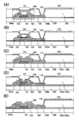
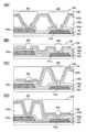
본 발명의 일 양태의 반도체 장치의 단면도를 도 1(A)에 나타낸다. 반도체 장치는 절연 표면(또는 절연 기판)(200)의 위에, 트랜지스터(100)와 전극(110)을 가진다. 트랜지스터(100)는 전극(101)과, 전극(101) 위의 절연층(102)과, 절연층(102) 위의 반도체층(103)과, 반도체층(103) 위의 절연층(105)과, 절연층(105) 위의 전극(106)을 가진다. 전극(101)은 절연층(102)을 통하여, 반도체층(103)과 중첩되는 영역을 가진다. 전극(106)은 절연층(105)을 통하여, 반도체층(103)과 중첩되는 영역을 가진다. 전극(110)은 절연층(105) 위에 설치된다. 영역(121)은 전극(106)의 적어도 일부가 반도체층(103)의 적어도 일부와 중첩되는 영역 중 적어도 일부의 영역이다. 영역(122)은 전극(110)이 설치된 영역 중 적어도 일부의 영역이다. 영역(121)에서의 절연층(105)은 영역(122)에서의 절연층(105)보다 얇다. 절연층(105)은 영역(121)과 영역(121)보다 두꺼운 영역(122)을 가지고, 영역(121)은 전극(106)과 반도체층(103)이 중첩되는 영역의 적어도 일부의 영역이며, 영역(122)은 전극(110)의 적어도 일부와 중첩한다고도 할 수 있다.Fig. 1A is a cross-sectional view of a semiconductor device according to one embodiment of the present invention. A semiconductor device has a
여기서, 전극(101)은 트랜지스터(100)의 제 1 게이트 전극으로서, 전극(106)은 트랜지스터(100)의 제 2 게이트 전극(백 게이트 전극)으로서 기능시킬 수 있다. 또한, 전극(110)은 화소 전극으로서 기능시킬 수 있다. 절연층(105)의 얇은 영역(영역(121))을 통하여 전극(106)은 반도체층(103)과 중첩되기 때문에, 전극(106)은 백 게이트 전극으로서 충분히 기능한다. 전극(110)과 전극(106)은 같은 도전막을 에칭함으로써 형성된 것이어도 좋다. 이 경우, 전극(110)과 전극(106)은 같은 재료를 가지고, 대체로 같은 막두께를 가진다. 또한, 전극(110)과 전극(106)은 다른 도전막을 에칭함으로써 형성된 것이어도 좋다. 같은 도전막을 에칭하는 경우에는, 프로세스 공정수를 저감할 수 있다.Here, the
또한, 트랜지스터는 제 1 게이트 전극과 제 2 게이트 전극(백 게이트 전극)을 양쪽 모두 가지는 것이 바람직하다. 단, 본 발명의 실시형태의 일 양태는 이것에 한정되지 않고, 제 1 게이트 전극 또는 제 2 게이트 전극(백 게이트 전극)의 어느 한쪽만을 가지고, 다른 한쪽을 갖지 않는 것도 가능하다. 예를 들면, 도 66(C)에 나타낸 바와 같이, 전극(106)을 갖지 않는 구성이어도 좋다. 그러한 경우에도, 트랜지스터로서 기능시킬 수 있다.Further, it is preferable that the transistor has both a first gate electrode and a second gate electrode (back gate electrode). However, one aspect of the embodiment of the present invention is not limited to this, and it is also possible to have only one of the first gate electrode and the second gate electrode (back gate electrode) and not the other. For example, as shown in FIG. 66(C) , a configuration in which the
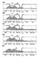
도 1(A)에서, 트랜지스터(100)는 전극(104a)과 전극(104b)을 더 가진다. 전극(104a)과 전극(104b)의 한쪽을 소스 전극으로 하고, 다른 한쪽을 드레인 전극으로 할 수 있다. 도 1(A)에서는 전극(104a)과 전극(104b)이 반도체층(103)의 상방에(예를 들면, 전극(104a)과 전극(104b)이 반도체층(103)의 상면 및 측면과 접하도록) 형성되어 있다. 반도체층(103)의 하면과, 전극(104a) 및 전극(104b)은 접하지 않는다.In FIG. 1A , the
또한, 트랜지스터는 소스 전극과 드레인 전극을 양쪽 모두 가지는 것이 바람직하다. 단, 본 발명의 실시형태의 일 양태는 이것에 한정되지 않고, 트랜지스터가 소스 전극 또는 드레인 전극의 어느 한쪽만을 가지고, 다른 한쪽을 갖지 않는 것도 가능하고, 양쪽 모두를 갖지 않는 것도 가능하다. 그러한 경우에도 이 트랜지스터가 반도체층(103)을 이용하여 다른 소자(예를 들면, 다른 트랜지스터)에 접속되도록 하면, 반도체층(103)에 채널이 형성되는 트랜지스터를 정상적으로 기능시킬 수 있다.In addition, it is preferable that the transistor has both a source electrode and a drain electrode. However, one aspect of the embodiment of the present invention is not limited to this, and it is possible that the transistor has only one of the source electrode and the drain electrode, does not have the other, or does not have both. Even in such a case, if this transistor is connected to another element (for example, another transistor) using the
또한, 트랜지스터란 게이트와, 드레인과, 소스를 포함하는 적어도 3개의 단자를 가지는 소자이다. 그리고, 드레인(드레인 단자, 드레인 영역 또는 드레인 전극)과 소스(소스 단자, 소스 영역 또는 소스 전극)의 사이에 채널 영역을 가지고 있고, 드레인과 채널 영역과 소스를 통하여 전류를 흘릴 수 있는 것이다. 여기서, 소스와 드레인은 트랜지스터의 구조 또는 동작 조건 등에 따라 바뀌기 때문에, 어느 것이 소스 또는 드레인인지를 한정하는 것이 곤란하다. 따라서, 소스로서 기능하는 부분, 및 드레인으로서 기능하는 부분을, 소스 또는 드레인이라고 부르지 않는 경우가 있다. 그 경우, 일례로서 소스와 드레인의 한쪽을 제 1 단자, 제 1 전극, 또는 제 1 영역이라고 표기하고, 소스와 드레인의 다른 한쪽을 제 2 단자, 제 2 전극, 또는 제 2 영역이라고 표기하는 경우가 있다.A transistor is an element having at least three terminals including a gate, a drain, and a source. In addition, a channel region is provided between the drain (drain terminal, drain region, or drain electrode) and the source (source terminal, source region, or source electrode), and current can flow through the drain, the channel region, and the source. Here, since the source and the drain change depending on the structure or operating conditions of the transistor, it is difficult to limit which one is the source or the drain. Therefore, the part functioning as a source and the part functioning as a drain may not be called a source or a drain. In that case, as an example, when one of the source and drain is denoted as the first terminal, the first electrode, or the first region, and the other of the source and the drain is denoted as the second terminal, the second electrode, or the second region. there is
전극(110)은 절연층(105)에 형성된 개구를 통하여, 트랜지스터(100)와 전기적으로 접속할 수 있다.The
또한, 「X의 위에 Y가」, 혹은, 「X 위에 Y가」라고 명시적으로 기재하는 경우는 X의 위에 Y가 직접 접하고 있는 것에 한정되지 않는다. 직접 접하지는 않는 경우, 즉, X와 Y의 사이에 다른 대상물이 개재하는 경우도 포함하는 것으로 한다. 여기서, X, Y는 대상물(예를 들면, 장치, 소자, 회로, 배선, 전극, 단자, 도전막, 층 등)인 것으로 한다.In addition, when "Y is on X" or "Y is on X" is explicitly described, it is not limited to the case where Y is in direct contact with X. The case where it does not come into direct contact, ie, the case where another object interposes between X and Y shall be included. Here, X and Y are assumed to be objects (for example, devices, elements, circuits, wirings, electrodes, terminals, conductive films, layers, etc.).
따라서 예를 들면, 「층 X의 위에(혹은 층 X 위에), 층 Y가」라고 명시적으로 기재되어 있는 경우는, 층 X의 위에 직접 접하여 층 Y가 있는 경우와, 층 X의 위에 직접 접하여 다른 층(예를 들면 층 Z 등)이 있고, 그 위에 직접 접하여 층 Y가 있는 경우를 포함하는 것으로 한다. 또한, 다른 층(예를 들면 층 Z 등)은 단층이어도 좋고, 복층(적층)이어도 좋다.Therefore, for example, when it is explicitly described as "on the layer X (or on the layer X), the layer Y", the case where the layer Y is directly on the layer X, It is assumed that there is another layer (for example, layer Z or the like) and there is a layer Y in direct contact thereon. In addition, a single layer may be sufficient as another layer (for example, layer Z etc.), and multiple layers (laminated) may be sufficient as it.
또한, 「X의 상방에 Y가」라고 명시적으로 기재되어 있는 경우에 대해서도 마찬가지이며, X의 위에 Y가 직접 접하고 있는 것에 한정되지 않고, X와 Y와의 사이에 다른 대상물이 개재하는 경우도 포함하는 것으로 한다. 따라서 예를 들면, 「층 X의 상방에, 층 Y가」라고 하는 경우는, 층 X의 위에 직접 접하여 층 Y가 있는 경우와, 층 X의 위에 직접 접하여 다른 층(예를 들면 층 Z 등)이 있고, 그 위에 직접 접하여 층 Y가 있는 경우를 포함하는 것으로 한다. 또한, 다른 층(예를 들면 층 Z 등)은 단층이어도 좋고, 복층(적층)이어도 좋다.In addition, the same applies to the case where "Y is above X" is explicitly described, and it is not limited to the case where Y is in direct contact on X, but also includes the case where another object is interposed between X and Y. do it by doing Therefore, for example, in the case of "above layer X, layer Y is", there is a case where there is a layer Y directly on top of the layer X and another layer (for example, layer Z, etc.) , and a case in which there is a layer Y in direct contact thereon is included. In addition, a single layer may be sufficient as another layer (for example, layer Z etc.), and multiple layers (laminated) may be sufficient as it.
또한, 「X 아래에 Y가」 혹은, 「X의 하방에 Y가」의 경우에 대해서도, 마찬가지이다.The same applies to the case of "Y is below X" or "Y is below X".
또한, 도 9(A)에 나타낸 바와 같이, 반도체층(103) 중 전극(104a) 및 전극(104b)과 중첩되지 않는 영역의 두께가 얇게 되어 있어도 좋다. 예를 들면, 전극(104a)과 전극(104b)을 제작하기 위한 에칭 가공을 할 때에, 전극(104a) 및 전극(104b)이 되는 층의 하층에 존재하는 반도체층(103)의 표면의 일부가 에칭되어도 좋다. 이렇게 하여, 반도체층(103) 중 채널이 되는 영역의 적어도 일부가 얇아진 트랜지스터(또는, 채널의 상부와 전극(104a) 및 전극(104b)과의 사이 등에 채널 보호막이 없는 트랜지스터)를, 채널 에칭형의 트랜지스터라고 부르는 경우가 있다.In addition, as shown in FIG. 9(A), the thickness of the area|region which does not overlap with the
본 발명의 반도체 장치의 일 양태는 도 1(A)에 한정되지 않는다. 이하에, 본 발명의 반도체 장치의 그 외의 구성의 예를 나타낸다. 또한, 도 1(A)과 같은 부분은 같은 부호를 이용하여 나타내고, 설명은 생략한다.One aspect of the semiconductor device of the present invention is not limited to FIG. 1A. Examples of other configurations of the semiconductor device of the present invention are shown below. In addition, the same part as FIG. 1(A) is shown using the same code|symbol, and description is abbreviate|omitted.
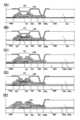
예를 들면, 도 1(B)에 나타낸 바와 같이, 반도체층(103)과 전극(104a)과 전극(104b)의 사이에 절연층(107)이 형성된 구성으로 할 수도 있다. 절연층(107)은 전극(104a)과 전극(104b)을 제작하기 위한 에칭 가공을 할 때에, 반도체층(103)(특히, 반도체층(103)의 채널이 되는 영역)이 에칭되는 것을 방지하기 위한 보호막(채널 보호막)으로서의 기능을 가진다. 채널 보호막이 형성된 트랜지스터를 채널 보호형의 트랜지스터라고 부르는 경우가 있다. 이 경우, 반도체층(103)을 얇게 할 수 있기 때문에, 트랜지스터(100)의 S값을 좋게(작게) 할 수 있다.For example, as shown in FIG. 1(B) , the insulating
또한, 채널 보호형의 트랜지스터로 하는 경우, 도 65(D)에 나타낸 바와 같이, 영역(121)에서 절연층(105)을 제거하는 것이 가능하다. 그 경우, 전극(106)과 절연층(107)은 일부에서 직접 접하는 구조가 된다. 이와 같이 함으로써, 전극(106)은 백 게이트 전극으로서, 보다 강한 전계를 반도체층(103)에 인가하는 것이 가능하게 된다.In the case of a channel protection type transistor, it is possible to remove the insulating
또는, 예를 들면, 도 2(A)에 나타낸 바와 같이, 전극(104a)과 전극(104b)은 반도체층(103)의 하방에(예를 들면, 전극(104a)과 전극(104b)의 상면 및 단면의 일부가 반도체층(103)의 하면과 접하도록) 형성해도 좋다. 이와 같이 함으로써, 반도체층(103)은 전극(104a)과 전극(104b)을 에칭할 때의 데미지를 받지 않게 할 수 있다. 또는, 반도체층(103)을 얇게 할 수 있어 S값을 좋게(S값을 작게) 할 수 있다.Alternatively, for example, as shown in FIG. 2A , the
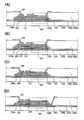
또는, 예를 들면, 도 3(A)에 나타낸 바와 같이, 반도체층(103)의 단부(131a) 및 단부(131b)와, 전극(104a) 및 전극(104b)의 단부(132a) 및 단부(132b)가, 대략 정렬된 형상으로 할 수도 있다. 동일한 마스크를 이용하여 에칭함으로써, 이러한 반도체층(103)과 전극(104a) 및 전극(104b)은 반도체막과 이 반도체막 위의 도전막과의 적층막을 형성할 수 있다. 이 마스크로서 노광에 이용하는 광의 투과율이 서로 다른 영역을 3개 이상 가지는 포토마스크(이하, 하프톤 마스크, 그레이톤 마스크, 위상 시프트 마스크, 또는 다계조 마스크라고 함)를 이용할 수 있다. 하프톤 마스크를 이용함으로써, 1장의 마스크를 이용한 에칭 공정에 의해, 반도체층(103)이 노출된 영역과 반도체층(103)이 제거된 영역을 형성할 수 있다. 이렇게 하여, 트랜지스터(100)의 제작 공정을 더욱 줄여, 더욱 반도체 장치의 저비용화를 실현할 수 있다. 또한, 하프톤 마스크를 이용하여 반도체층(103)과 전극(104a) 및 전극(104b)을 형성한 경우, 전극(104a) 및 전극(104b)의 아래에는, 반드시 반도체층(103)이 존재하는 구성이 된다. 또한, 단부(132a) 및/또는 단부(132b)는 계단 형상으로 되어 있는 경우도 있다.Alternatively, for example, as shown in FIG. 3A , the
또는, 도 3(B)에 나타낸 바와 같이, 도 3(A)에 나타낸 구성에서 채널 보호막으로서 기능하는 절연층(107)을 형성할 수도 있다. 이와 같이, 도 3(B) 이외의 경우에도, 채널 보호막을 형성하지 않은 다양한 트랜지스터에서, 채널 보호막을 추가하여 형성할 수 있다.Alternatively, as shown in Fig. 3B, an insulating
또는, 예를 들면, 도 9(A)에 나타낸 바와 같이, 반도체층(103)과 전극(104a) 및 전극(104b)과의 사이에, 도전층(108a) 및 도전층(108b)을 가지는 구성으로 할 수도 있다. 도전층(108a) 및 도전층(108b)은 예를 들면, 도전성을 부여하는 불순물 원소가 첨가된 반도체층을 이용하여 형성할 수 있다. 또는, 예를 들면, 도전층(108a) 및 도전층(108b)은 도전성의 금속 산화물을 이용하여 형성할 수도 있다. 또는, 예를 들면, 도전층(108a) 및 도전층(108b)은 도전성을 부여하는 불순물 원소가 첨가된, 도전성의 금속 산화물을 이용하여 형성할 수도 있다. 또한, 도 1(A) 등의 경우에, 반도체층(103)의 일부의 영역에, 도전성을 부여하는 불순물 원소가 첨가되어 있어도 좋다. 도전성을 부여하는 불순물 원소의 일례로서 인, 비소, 붕소, 수소, 주석 등이 있다.Alternatively, for example, as shown in Fig. 9(A) , a structure including a
여기서, 도 9(A)에서 반도체층(103) 중, 전극(104a) 및 전극(104b), 및, 도전층(108a) 및 도전층(108b)과 중첩되지 않는 영역에서는, 두께가 얇게 되어 있다. 이것은 전극(104a)과 전극(104b), 및, 도전층(108a) 및 도전층(108b)을 제작하기 위한 에칭 가공을 할 때에, 전극(104a)과 전극(104b)이 되는 층, 및, 도전층(108a) 및 도전층(108b)이 되는 층의 하층에 존재하는 반도체층(103)의 표면의 일부가 에칭되기 때문이다(채널 에칭형의 트랜지스터). 또한, 반도체층(103)과 도전층(108a) 및 도전층(108b)의 사이에 채널 보호막을 형성함으로써, 반도체층(103)이 에칭되는 것을 방지해도 좋다(채널 보호형의 트랜지스터).Here, in the
또한, 상기에서는 전극(110) 및 전극(106)이 같은 층을 이용하여 형성된 구성을 나타냈지만 이것에 한정되지 않고, 전극(110)과 전극(106)은 다른 층을 이용하여 형성되어 있어도 좋다.In addition, although the structure in which the
또는, 전극(104a) 및 전극(104b)과, 반도체층(103)와의 사이, 또는, 전극(104a) 및 전극(104b)과, 도전층(108a) 및 도전층(108b)의 사이에서, 절연층을 형성하는 것이 가능하다. 그리고, 그 절연층에 개구를 형성하고, 전극(104a) 및 전극(104b)과, 반도체층(103)을 접속, 또는, 전극(104a) 및 전극(104b)과, 도전층(108a) 및 도전층(108b)을 접속하도록 해도 좋다.Alternatively, insulation is provided between the
또한, 절연 표면(200)을 가지는 기판으로서는, 다양한 기판을 이용할 수 있다. 기판의 종류는 특정의 것에 한정되는 것은 아니다. 기판의 일례로서는, 반도체 기판(예를 들면 단결정 기판 또는 실리콘 기판), SOI 기판, 유리 기판, 석영 기판, 플라스틱 기판, 금속 기판, 스테인리스 스틸 기판, 스테인리스 스틸 포일을 가지는 기판, 텅스텐 기판, 텅스텐 포일을 가지는 기판, 가요성 기판, 부착 필름, 섬유 형상의 재료를 포함하는 종이, 또는 기재 필름 등이 있다.In addition, as the substrate having the insulating
또한, 트랜지스터(100)를 기판 위에 형성하고, 그 후, 이 기판과는 다른 기판에 트랜지스터(100)를 옮김으로써, 이 다른 기판 위에 트랜지스터(100)를 배치해도 좋다.Alternatively, the
상기에 설명한 바와 같이, 도 1(A), 도 1(B), 도 2(A), 도 3(A), 도 3(B), 도 9(A) 등에 나타낸 트랜지스터(100)에서는, 백 게이트 전극에 의해, 스레숄드 전압을 효과적으로 제어하는 것이 가능하게 된다. 따라서, 노멀리 오프 상태가 되기 쉽게 할 수 있다. 또는, 백 게이트 전극에 의해, 온 전류를 효과적으로 크게 할 수 있다. 또는, 백 게이트 전극에 의해, 오프 전류를 효과적으로 작게 할 수 있다. 또는, 백 게이트 전극에 의해, 온 오프비를 크게 할 수 있다. 따라서, 상기 구성을 표시 장치에 채용함으로써, 표시 장치는 정확한 표시를 행할 수 있다. 또는, 상기 구성을 표시 장치나 발광 장치에 채용하여, 절연층(105)을 평탄화막으로서도 기능시킴으로써, 개구율을 높게 할 수 있다.As described above, in the
본 실시형태는 본 발명의 일 양태인 구성예 중 기본적인 예의 하나이다. 따라서, 그 일부 또는 전부에 대하여, 변경, 추가, 수정, 삭제, 응용, 상위 개념화, 또는, 하위 개념화한 것에 상당하는 다른 실시형태와 자유롭게 조합하여 실시할 수 있다.This embodiment is one of the basic examples among the structural examples which are one aspect of this invention. Accordingly, part or all of the changes, additions, corrections, deletions, applications, higher-level conceptualizations, or lower-level conceptualizations can be freely combined with other embodiments corresponding to the implementations.
(실시형태 2)(Embodiment 2)
본 실시형태에서는, 본 발명의 반도체 장치 등(표시 장치, 발광 장치 등)의 일 양태에 대하여 도면을 참조하여 설명한다.In this embodiment, one aspect of the semiconductor device etc. (display device, light emitting device, etc.) of this invention is demonstrated with reference to drawings.
실시형태 1에 있어서, 도 1(A), 도 1(B), 도 2(A), 도 3(A), 도 3(B), 도 9(A) 등을 이용하여 나타낸 구성에서, 영역(122) 또는 그 일부에서의 절연층(105)을 복수의 층의 적층으로 할 수 있다. 영역(122) 또는 그 일부에서의 절연층(105)은 m(M은 2이상의 자연수)개의 층의 적층을 가진다. 영역(121) 또는 그 일부에서의 절연층(105)은 m과 같거나, 또는, m보다 적은 갯수의 층의 적층 또는 단층을 가지고 있어도 좋다. 또는, 절연층(105)은 유기 절연층을 포함하고 있어도 좋다. 절연층(105)은 유기 절연층과 무기 절연층의 적층을 포함하고 있어도 좋다.In
예를 들면, 상기한 도 1(A), 도 1(B), 도 2(A), 도 3(A), 도 3(B), 도 9(A) 등에 나타낸 구성에서, 영역(122)에서의 절연층(105)은 층(105a)과 층(105b)의 적층을 가지고, 영역(121)에서의 절연층(105)은 층(105a)의 단층을 가져도 좋다. 층(105b)은 층(105a)보다 위에 형성되어 있다. 이러한 구성을 도 1(C), 도 1(D), 도 2(B), 도 3(C), 도 3(D), 도 9(B)에 나타낸다. 이러한 구성으로 함으로써, 에칭의 용이성의 차이(선택비)를 이용하여, 필요한 부분만 에칭함으로써, 층(105a)과 층(105b)의 적층을 형성할 수 있다. 그 결과, 절연층(105)의 각 영역에서의 막두께를 제어하기 쉽게 할 수 있다. 또는, 막질에 따라 다른 기능(예를 들면, 평탄화 기능, 불순물을 차단하는 기능, 차광하는 기능 등)을 각 영역에 적절히 갖게 할 수 있다. 또는, 감광성 재료를 이용하여 일부의 층을 형성함으로써, 프로세스 공정수를 줄일 수 있다.For example, in the configuration shown in Fig. 1 (A), Fig. 1 (B), Fig. 2 (A), Fig. 3 (A), Fig. 3 (B), Fig. 9 (A), etc., the
여기서, 층(105a)을 무기 절연층으로 하고, 층(105b)을 유기 절연층으로 해도 좋다. 그 경우, 유기 재료를 이용하기 때문에, 층(105a)보다 층(105b)을 두껍게 하는 것이 가능하다. 층(105a)을 무기 절연층(보다 바람직하게는, 질화규소막)으로 함으로써, 예를 들면 층(105b) 중의 불순물이 트랜지스터(100)에 진입하는 것을 방지할 수 있다. 또는, 층(105b)을 유기 절연층으로 함으로써, 이 유기 절연층을 평탄화층으로서 기능시킬 수 있기 때문에, 트랜지스터(100) 등에 의한 요철을 완화할 수 있다. 이렇게 하여, 전극(110)이 형성되는 표면을 평탄하게 할 수 있다. 따라서, 예를 들면, 전극(110)을 화소 전극으로서 이용하는 경우에, 표시 불량을 저감할 수 있다. 또는, 층(105b)의 막두께를 두껍게 할 수 있기 때문에, 화소 전극에의 노이즈를 줄일 수 있다. 또는, 막질에 따라 에칭의 선택비가 다르기 때문에, 필요한 부분만을 선택적으로 에칭하여, 소정의 형상의 층(105a) 및 층(105b)의 적층을 형성할 수 있다.Here, the
또는, 층(105a) 및/또는 층(105b)(또는 그들의 일부)를(보다 바람직하게는 층(105b)을), 컬러 필터 및/또는 블랙 매트릭스로 해도 좋다. 컬러 필터 및/또는 블랙 매트릭스로 함으로써, 트랜지스터(100)가 설치된 기판(절연 표면(200)을 가지는 기판)과 다른 기판(예를 들면, 표시 장치에서의 대향 기판 등)과의 부착 마진을 크게 할 수 있다. 또는, 트랜지스터(100)의 근방의 층(105a) 및/또는 층(105b)(또는 그들의 일부)에, 블랙 매트릭스를 이용함으로써, 트랜지스터(100)에 광이 들어가기 어렵게 할 수 있다. 광이 들어가기 어려우므로, 트랜지스터(100)의 오프 전류나, 트랜지스터(100)의 열화를 저감하는 것이 가능하게 된다. 예를 들면, 도 65(A)에 나타낸 바와 같이, 층(105b)의 일부에서, 블랙 매트릭스(652)를 형성할 수 있다. 또한, 블랙 매트릭스로서 색이 다른 컬러 필터를 복수 중첩하는 구성을 이용할 수도 있다.Alternatively, the
또한, 컬러 필터 및/또는 블랙 매트릭스는 유기 재료를 이용하여 형성하는 것이 바람직하기 때문에, 층(105b)에서 형성되는 것이 바람직하다. 단, 이것에 한정되지 않고, 블랙 매트릭스로서, 차광성을 가지는 도전막을 이용할 수도 있다.Further, since the color filter and/or the black matrix is preferably formed using an organic material, it is preferably formed in the
또는, 층(105a)의 막두께를 층(105b)의 막두께보다 얇게 해도 좋다. 층(105a)의 막두께를 얇게 함으로써, 전극(106)에 의한 전계를 채널에 충분히 공급할 수 있다. 또는, 층(105b)의 막두께를 두껍게 함으로써, 트랜지스터(100) 등에 의한 요철을 충분히 완화할 수 있다.Alternatively, the film thickness of the
또는, 예를 들면, 상기한 도 1(A), 도 1(B), 도 2(A), 도 3(A), 도 3(B), 도 9(A) 등에 나타낸 구성에 있어서, 영역(122)에서의 절연층(105)은 층(105b)과 층(105c)의 적층을 가지고, 영역(121)에서의 절연층(105)은 층(105c)의 단층을 가져도 좋다. 층(105c)은 층(105b)보다 위에 형성되어 있다. 이러한 구성을 도 26(A), 도 26(B), 도 27(A), 도 28(A), 도 28(B), 도 34(A)에 나타낸다. 이러한 구성으로 함으로써, 에칭의 용이성의 차이(선택비)를 이용하여, 필요한 부분만 에칭함으로써, 층(105b)과 층(105c)의 적층을 형성할 수 있다. 그 결과, 절연층(105)의 각 영역에서의 막두께를 제어하기 쉽게 할 수 있다. 또는, 막질에 따라 다른 기능(예를 들면, 평탄화 기능, 불순물을 차단하는 기능, 차광하는 기능 등)을 각 영역에 적절히 갖게 할 수 있다. 또는, 일부의 층은 감광성 재료를 이용하여 형성할 수 있기 때문에, 프로세스 공정수를 줄일 수 있다.Or, for example, in the configuration shown in Fig. 1 (A), Fig. 1 (B), Fig. 2 (A), Fig. 3 (A), Fig. 3 (B), Fig. 9 (A), etc., the region The insulating
여기서, 층(105b)을 유기 절연층으로 하고, 층(105c)을 무기 절연층으로 해도 좋다. 그 경우, 유기 재료를 이용하기 때문에, 층(105c)보다 층(105b)을 두껍게 하는 것이 가능하다. 층(105c)을 무기 절연층(보다 바람직하게는, 질화규소막)으로 함으로써, 층(105b) 중의 불순물이 전극(106)이나 전극(106) 위에 형성되는 층(예를 들면, 액정층, 배향막, 유기 EL층 등)에 진입하는 것을 방지할 수 있다. 또는, 층(105b)을 유기 절연층으로 함으로써, 이 유기 절연층을 평탄화층으로서 이용하여 트랜지스터(100) 등에 의한 요철을 완화할 수 있다. 이렇게 하여, 전극(110)이 형성되는 표면을 평탄하게 할 수 있다. 따라서, 예를 들면, 전극(110)을 화소 전극으로서 이용하는 경우에, 표시 불량을 저감할 수 있다. 또는, 층(105b)의 막두께를 두껍게 할 수 있기 때문에, 화소 전극에의 노이즈를 줄일 수 있다. 또는, 막질이 다른 것에 의해 에칭의 선택비가 다르기 때문에, 필요한 부분만을 선택적으로 에칭하여, 소정의 형상의 층(105b) 및 층(105c)의 적층을 형성할 수 있다.Here, the
또는, 층(105b) 및/또는 층(105c)(또는 그들의 일부)을(보다 바람직하게는 층(105b)을), 컬러 필터 및/또는 블랙 매트릭스로 해도 좋다. 컬러 필터 및/또는 블랙 매트릭스로 함으로써, 트랜지스터(100)가 설치된 기판(절연 표면(200)을 가지는 기판)과 다른 기판(예를 들면, 표시 장치에서의 대향 기판 등)과의 부착 마진을 크게 할 수 있다. 또는, 트랜지스터(100)의 근방의 층(105b) 및/또는 층(105c)(또는 그들의 일부)에, 블랙 매트릭스를 이용함으로써, 트랜지스터(100)에 광이 들어가기 어렵게 할 수 있다. 광이 들어가기 어려우므로, 트랜지스터(100)의 오프 전류를 저감 및/또는 트랜지스터(100)의 열화를 저감하는 것이 가능하게 된다. 예를 들면, 도 65(B)에 나타낸 바와 같이, 층(105b)의 일부에서, 블랙 매트릭스(652)를 형성할 수 있다. 또한, 블랙 매트릭스로서 색이 다른 컬러 필터를 복수 중첩하는 구성을 이용할 수도 있다.Alternatively, the
또한, 컬러 필터 및/또는 블랙 매트릭스는 유기 재료를 이용하여 형성하는 것이 바람직하기 때문에, 층(105b)에서 형성되는 것이 바람직하다. 단, 이것에 한정되지 않고, 블랙 매트릭스로서 차광성을 가지는 도전막을 이용할 수도 있다.Further, since the color filter and/or the black matrix is preferably formed using an organic material, it is preferably formed in the
또는, 층(105c)의 막두께를 층(105b)의 막두께보다 얇게 해도 좋다. 층(105c)의 막두께를 얇게 함으로써, 전극(106)에 의한 전계를 채널에 충분히 공급할 수 있다. 또는, 층(105b)의 막두께를 두껍게 함으로써, 트랜지스터(100) 등에 의한 요철을 충분히 완화할 수 있다.Alternatively, the film thickness of the
또는, 예를 들면, 상기한 도 1(A), 도 1(B), 도 2(A), 도 3(A), 도 3(B), 도 9(A) 등에 나타낸 구성에서, 영역(122)에서의 절연층(105)은 층(105a)과 층(105b)과 층(105c)의 적층을 가지고, 영역(121)에서의 절연층(105)은 층(105a)과 층(105c)의 적층을 가져도 좋다. 이러한 구성을 도 26(C), 도 26(D), 도 27(B), 도 28(C), 도 28(D), 도 34(B)에 나타낸다. 이러한 구성으로 함으로써, 에칭의 용이성의 차이(선택비)를 이용하여, 필요한 부분만 에칭함으로써, 층(105a)과 층(105b)과 층(105c)의 적층을 형성할 수 있다. 그 결과, 절연층(105)의 각 영역에서의 막두께를 제어하기 쉽게 할 수 있다. 또는, 막질에 따라 다른 기능(예를 들면, 평탄화 기능, 불순물을 차단하는 기능, 차광하는 기능 등)을 각 영역에 적절히 갖게 할 수 있다. 또는, 일부의 층은 감광성 재료를 이용하여 형성할 수 있기 때문에, 프로세스 공정수를 줄일 수 있다.Or, for example, in the configuration shown in Fig. 1 (A), Fig. 1 (B), Fig. 2 (A), Fig. 3 (A), Fig. 3 (B), Fig. 9 (A), etc., the region ( The insulating
여기서, 층(105a)을 무기 절연층으로 하고, 층(105b)을 유기 절연층으로 하고, 층(105c)을 무기 절연층으로 해도 좋다. 그 경우, 유기 재료를 이용하기 때문에, 층(105a) 및 층(105c)보다 층(105b)을 두껍게 하는 것이 가능하다. 층(105a)을 무기 절연층(보다 바람직하게는, 질화규소막)으로 함으로써, 예를 들면, 층(105b) 중의 불순물이 트랜지스터(100)에 진입하는 것을 방지할 수 있다. 또는, 층(105c)을 무기 절연층(보다 바람직하게는, 질화규소막)으로 함으로써, 층(105b) 중의 불순물이 전극(106)이나 전극(106) 위에 형성되는 층에 진입하는 것을 방지할 수 있다. 층(105b)을 유기 절연층으로 함으로써, 이 유기 절연층을 평탄화층으로서 이용하여 트랜지스터(100) 등에 의한 요철을 완화할 수 있다. 이렇게 하여, 전극(110)이 형성되는 표면을 평탄하게 할 수 있다. 따라서, 예를 들면, 전극(110)을 화소 전극으로서 이용하는 경우에, 표시 불량을 저감할 수 있다. 또는, 층(105b)의 막두께를 두껍게 할 수 있기 때문에, 화소 전극에의 노이즈를 줄일 수 있다. 또는, 층(105a)과 층(105b), 또는, 층(105b)과 층(105c)의 막질을 다르게 할 수 있다. 그리고, 막질에 따라 에칭의 선택비가 다른 것을 이용하여, 필요한 부분만을 선택적으로 에칭하여, 소정의 형상의 층(105a)과 층(105b)과 층(105c)의 적층을 형성할 수 있다.Here, the
또는, 층(105a), 층(105b) 및/또는 층(105c)(또는 그들의 일부)을(보다 바람직하게는 층(105b)을), 컬러 필터 및/또는 블랙 매트릭스로 해도 좋다. 컬러 필터 및/또는 블랙 매트릭스로 함으로써, 트랜지스터(100)가 설치된 기판(절연 표면(200)을 가지는 기판)과 다른 기판(예를 들면, 표시 장치에서의 대향 기판 등)과의 부착 마진을 크게 할 수 있다. 또는, 트랜지스터(100)의 근방의 층(105a), 층(105b) 및/또는 층(105c)(또는 그들의 일부)에, 블랙 매트릭스를 이용함으로써, 트랜지스터(100)에 광이 들어가기 어렵게 할 수 있다. 광이 들어가기 어려우므로, 트랜지스터(100)의 오프 전류를 저감 및/또는 트랜지스터(100)의 열화를 저감하는 것이 가능하게 된다. 예를 들면, 도 65(C)에 나타낸 바와 같이, 층(105b)의 일부에서, 블랙 매트릭스(652)를 형성할 수 있다. 또한, 블랙 매트릭스로서 색이 다른 컬러 필터를 복수 중첩하는 구성을 이용할 수도 있다.Alternatively, the
또한, 컬러 필터 및/또는 블랙 매트릭스는 유기 재료를 이용하여 형성하는 것이 바람직하기 때문에, 층(105b)에서 형성되는 것이 바람직하다. 단, 이것에 한정되지 않고, 블랙 매트릭스로서 차광성을 가지는 도전막을 이용할 수도 있다.Further, since the color filter and/or the black matrix is preferably formed using an organic material, it is preferably formed in the
또한, 층(105a), 층(105b), 층(105c)은 각각 한 개의 층이어도, 복수개의 층의 적층이어도 좋다.In addition, the
본 실시형태는 실시형태 1의 일부 또는 전부에 대하여, 변경, 추가, 수정, 삭제, 응용, 상위 개념화, 또는, 하위 개념화한 것에 상당한다. 따라서, 실시형태 1 등의 다른 실시형태와 자유롭게 조합하는 것이나, 치환하여 실시할 수 있다.This embodiment corresponds to a change, addition, correction, deletion, application, super-conceptualization, or sub-conceptualization of some or all of the first embodiment. Therefore, it can be freely combined with other embodiments, such as
(실시형태 3)(Embodiment 3)
본 실시형태에서는, 본 발명의 반도체 장치 등(표시 장치, 발광 장치 등)의 일 양태에 대하여 도면을 참조하여 설명한다.In this embodiment, one aspect of the semiconductor device etc. (display device, light emitting device, etc.) of this invention is demonstrated with reference to drawings.
실시형태 1에서, 도 1(A), 도 1(B), 도 2(A), 도 3(A), 도 3(B), 도 9(A) 등을 이용하여 나타낸 구성에서는, 트랜지스터(100)의 채널 근방에서 절연층(105)을 얇게 하는 구성을 나타냈다. 그러나, 절연층(105)을 얇게 하는 영역(영역(121))의 범위는 이것에 한정되지 않는다. 영역(121)의 범위는 채널 근방의 일부이어도 좋다. 예를 들면, 도 1(A)에 나타낸 구성은 도 66(A)에 나타낸 구성으로 변경할 수 있다. 도 66(A)에서는 영역(121)의 범위는 채널 근방의 일부(도 1(A)에서의 영역(121)보다 좁은 범위)이다. 도 1(A) 이외의 도면의 구성도 이와 같이 변경할 수 있다. 또는, 영역(121)의 범위는 트랜지스터(100)의 전체 근방이어도 좋고, 좀 더 넓은 범위여도 좋다. 예를 들면, 트랜지스터(100)의 근방(예를 들면, 전극(106)이 전극(104a) 및/또는 전극(104b)과 중첩되는 영역)에서, 절연층(105)을 얇게 하는 구성이어도 좋다.In
또한, 실시형태 2에서, 도 1(C), 도 1(D), 도 2(B), 도 3(C), 도 3(D), 도 9(B), 도 26(A), 도 26(B), 도 27(A), 도 28(A), 도 28(B), 도 34(A), 도 26(C), 도 26(D), 도 27(B), 도 28(C), 도 28(D), 도 34(B), 도 65(A), 도 65(B), 도 65(C) 등에 나타낸 구성에서는, 트랜지스터(100)의 채널 근방의 층(105b)을 제거하여, 절연층(105)을 얇게 하는 구성을 나타냈다. 그러나, 층(105b)을 제거하는 영역은 이것에 한정되지 않는다. 층(105b)을 제거하는 영역은 채널 근방의 일부이어도 좋다. 예를 들면, 도 1(C)에 나타낸 구성은 도 66(B)에 나타낸 구성으로 변경할 수 있다. 도 66(B)에서는 영역(121)의 범위는 채널 근방의 일부(도 1(C)에서의 영역(121)보다 좁은 범위)이다. 도 1(C) 이외의 도면의 구성도 이와 같이 변경할 수 있다. 또는, 영역(121)의 범위는 트랜지스터(100)의 전체 근방이어도 좋고, 좀 더 넓은 범위여도 좋다. 예를 들면, 도 1(C), 도 1(D), 도 2(B), 도 3(C), 도 3(D), 도 9(B), 도 26(C), 도 26(D), 도 27(B), 도 28(C), 도 28(D), 도 34(B)에 나타낸 구성에서, 트랜지스터(100)의 근방의 층(105b)을 제거하여, 절연층(105)을 얇게 해도 좋다. 예를 들면, 전극(106)이 전극(104a) 및/또는 전극(104b)과 중첩되는 영역에서 층(105b)을 제거해도 좋다. 이 구성을 도 1(E), 도 2(D), 도 2(C), 도 3(E), 도 2(E), 도 9(C), 도 26(E), 도 27(D), 도 27(C), 도 28(E), 도 27(E), 도 34(C)에 나타낸다.Moreover, in
또한, 도 26(E), 도 27(D), 도 27(C), 도 28(E), 도 27(E), 도 34(C)에 나타낸 구성에서, 층(105b)을 제거한 영역의 일부 또는 전부에서, 층(105a) 또는 층(105c)의 한쪽을 더 제거해도 좋다.Further, in the configuration shown in Figs. 26(E), 27(D), 27(C), 28(E), 27(E), and 34(C), the region from which the
트랜지스터(100)의 근방(예를 들면, 전극(106)이 전극(104a) 및/또는 전극(104b)과 중첩되는 영역)에서, 절연층(105)을 얇게 하는 구성에서는, 전극(106)이 전극(104a) 및/또는 전극(104b)과 중첩됨으로써 형성되는 기생 용량의 용량값을 크게 할 수 있다. 따라서, 이 기생 용량을 보유 용량으로서 적극적으로 이용할 수도 있다. 예를 들면, 이 보유 용량을 화소의 보유 용량으로서 이용할 수 있다. 이와 같이 트랜지스터(100)의 근방에서, 절연층(105)을 얇게 한다고 해도, 전극(106)에 일정한 전위가 부여된 경우에, 이 전위는 전극(104a) 및/또는 전극(104b)의 전위에 영향을 주지 않는다. 단, 본 발명의 실시형태의 일 양태는 이것에 한정되지 않는다.In a configuration in which the insulating
한편, 전극(106)에 변동하는 전위(펄스 전위 등)를 부여하는 경우(예를 들면, 전극(101)에 입력되는 신호와 같은 신호가 전극(106)에 입력되는 경우 등)에는 전극(106)에 부여할 수 있는 전위의 변화가 전극(104a) 및/또는 전극(104b)의 전위에 주는 영향을 저감하기 위해, 전극(106)과 전극(104a) 및/또는 전극(104b)과의 사이에서, 절연층(105)의 두께를 두껍게 하는 것이 바람직하다. 예를 들면, 전극(106)과 전극(104a) 및/또는 전극(104b)과의 사이에 층(105b)이 존재하는 것이 바람직하다. 이렇게 하여, 전극(106)에 부여되는 전위의 변화가 전극(104a) 및/또는 전극(104b)의 전위에 주는 영향을 저감하여, 예를 들면, 전극(104b)과 접속된 전극(110)에 입력되는 신호에 노이즈가 들어가는 것을 방지할 수 있다. 따라서, 전극(110)을 화소 전극으로 한 경우에, 표시 장치의 표시 품질을 좋게 할 수 있다. 단, 본 발명의 실시형태의 일 양태는 이것에 한정되지 않는다.On the other hand, when a variable potential (pulse potential, etc.) is applied to the electrode 106 (eg, when a signal identical to a signal input to the
또한, 영역(121) 전체에 전극(106)이 형성되어 있어도 좋고, 영역(121)의 적어도 일부에 전극(106)이 형성되어 있어도 좋다. 전극(106)이 작은 경우는 전극(104a) 및/또는 전극(104b)과 전극(106)과의 중첩이 작아지기 때문에, 전극(106)에 부여되는 전위의 변화가 전극(104a) 및/또는 전극(104b)의 전위에 주는 영향을 저감할 수 있다.In addition, the
또는, 트랜지스터(100)를 이용하여 구동 회로(예를 들면, 화소에 신호를 입력하는 주사선 구동 회로나 신호선 구동 회로)를 형성하는 경우, 구동 회로 위의 전체를 영역(121)으로 해도 좋다. 예를 들면, 구동 회로 위의 층(105b) 전체를 제거해도 좋다. 이것은, 구동 회로 위에는 화상 표시를 행하기 위한 표시 소자를 형성할 필요가 없기 때문에, 층(105b)에 의한 평탄화를 행하지 않아도 좋기 때문이다. 또는, 구동 회로 위의 층(105b) 전체를 제거함으로써, 전극이나 배선에 의해 형성되는 용량 소자(기생 용량)를 크게 할 수 있다. 이렇게 하여, 부트스트랩 동작을 행하기 위한 용량 소자(기생 용량)나, 다이나믹 회로용의 용량 소자(기생 용량)를 크게 할 수 있다. 또는, 구동 회로 위의 층(105b) 전체를 제거하는 경우, 층(105b)의 일부를 남기기 위한 마진이 필요 없기 때문에, 구동 회로 전체의 레이아웃 면적을 작게 할 수 있다. 이 경우에, 구동 회로에 포함되는 트랜지스터(100) 중 복수의 트랜지스터(100)의 전극(106)은 서로 전기적으로 접속되어 있어도 좋다. 또는, 구동 회로에 포함되는 트랜지스터(100) 중 복수의 트랜지스터(100)에서, 전극(106)은 서로 분리되어 있어도 좋고, 분리되어 있지 않아도 좋다.Alternatively, when a driver circuit (eg, a scan line driver circuit or a signal line driver circuit for inputting a signal to a pixel) is formed using the
본 실시형태는 실시형태 1 내지 실시형태 2의 일부 또는 전부에 대하여, 변경, 추가, 수정, 삭제, 응용, 상위 개념화, 또는, 하위 개념화한 것에 상당한다. 따라서, 실시형태 1 내지 실시형태 2 등의 다른 실시형태와 자유롭게 조합하거나, 치환하여 실시할 수 있다.This embodiment corresponds to a change, addition, correction, deletion, application, super-conceptualization, or sub-conceptualization of some or all of the first to second embodiments. Therefore, it can freely combine with other embodiments, such as Embodiment 1 -
(실시형태 4)(Embodiment 4)
본 실시형태에서는, 본 발명의 반도체 장치 등(표시 장치, 발광 장치 등)의 일 양태에 대하여 도면을 참조하여 설명한다.In this embodiment, one aspect of the semiconductor device etc. (display device, light emitting device, etc.) of this invention is demonstrated with reference to drawings.
실시형태 1 내지 실시형태 3에서 나타낸 반도체 장치 등의 구성예에서, 전극(110)과 전극(104b)의 접속 부분의 구성예에 대하여 나타낸다.In the structural example of the semiconductor device etc. shown in Embodiment 1 -
절연층(105)이 층(105a)과 층(105b)의 적층을 가지는 경우의 전극(110)과 전극(104b)의 접속 부분의 구성예에 대하여, 도 4 및 도 5를 이용하여 설명한다.A configuration example of the connection portion between the
도 4(A)는 도 1(C)에 나타낸 구성과, 이 구성에서의 전극(110)과 전극(104b)의 접속 부분을 확대한 도면이다. 도 4(A)의 확대도에서 층(105a)의 개구의 단부와 층(105b)의 개구의 단부는 대략 정렬된 형상으로 되어 있다. 이러한 개구는, 예를 들면, 층(105a)이 되는 막 A와, 층(105b)이 되는 막 B의 적층막을 형성한 후, 같은 포토마스크를 이용하여, 막 A와 막 B를 에칭 가공함으로써 형성할 수 있다.FIG. 4A is an enlarged view of the configuration shown in FIG. 1C and the connection portion between the
전극(110)과 전극(104b)의 접속 부분의 형상은 도 4(A)의 확대도에 나타낸 구성에 한정되지 않는다. 예를 들면, 도 4(B)에 나타낸 구성으로 해도 좋다. 도 4(B)에서는 층(105a)의 개구의 단부와 층(105b)의 개구의 단부는 정렬되지 않고, 층(105b)의 개구의 직경은 층(105a)의 개구의 직경보다 크다(개구의 직경의 차를 도면 중 Δx1로 나타냄). 이러한 형상의 개구는 예를 들면, 도 4(A)의 확대도에 나타낸 구성을 제작한 후, 층(105b)을 애싱함으로써 형성할 수 있다. 층(105b)을 애싱하는 경우에는, 층(105b)은 유기 절연층에 의해 형성한다. 또한, 애싱이란, 방전 등에 의해 생성한 활성 산소 분자 혹은 오존 분자 혹은 산소 원자 등을 유기물인 층에 화학적으로 작용시켜 회화(灰化)시킴으로써 층의 일부를 제거하는 것이다. 또는, 층(105a)이 되는 막 A와, 층(105b)이 되는 막 B의 적층막을 형성한 후, 포토마스크에 의해 막 A와 막 B를 에칭 가공한 후, 다른 포토마스크에 의해, 에칭 가공된 막 B를 더 에칭 가공함으로써 형성할 수도 있다. 또는, 층(105a)이 되는 막 A와, 층(105b)이 되는 막 B의 적층막을 형성한 후, 포토마스크에 의해 막 B를 에칭 가공한 후, 다른 포토마스크에 의해 막 A를 에칭 가공함으로써 형성할 수도 있다. 막 A와 막 B를 다른 포토마스크에 의해 에칭 가공하는 경우에는, 예를 들면, 도 5(B)에 나타낸 바와 같이, 도 4(B)에 나타낸 구성보다, 층(105b)의 개구의 직경을 층(105a)의 개구의 직경보다 더욱 크게 할 수도 있다(개구의 직경의 차를 도면 중 Δx3로 나타냄). 또는, 막 A와 막 B를 다른 포토마스크에 의해 에칭 가공하는 경우에는, 예를 들면, 도 5(A)에 나타낸 바와 같이, 층(105a)의 개구의 직경을 층(105b)의 개구의 직경보다 크게 할 수도 있다(개구의 직경의 차를 도면 중 Δx2로 나타냄).The shape of the connection part of the
도 4 및 도 5에서는 절연층(105)이 층(105a)과 층(105b)의 적층으로 이루어지는 경우의 전극(110)과 전극(104b)의 접속 부분의 구성예에 대하여 나타냈다. 그러나, 절연층(105)의 적층 구조는 이것에 한정되지 않기 때문에, 이 적층 구조에 따라, 전극(110)과 전극(104b)의 접속 부분은 다양한 구성으로 할 수 있다.4 and 5 show examples of the configuration of the connection portion between the
예를 들면, 절연층(105)이 층(105b)과 층(105c)의 적층으로 이루어지는 경우의 전극(110)과 전극(104b)의 접속 부분의 구성예에 대하여 도 29에 나타낸다. 도 29(A)는 도 26(A)에 나타낸 구성과, 이 구성에서의 전극(110)과 전극(104b)의 접속 부분을 확대한 도면이다. 도 29(A)에서는 층(105b)의 개구의 단부와 층(105c)의 개구의 단부는 정렬되지 않고, 층(105b)의 개구의 직경은 층(105c)의 개구의 직경보다 크다. 도 29(B)에서는 층(105b)의 개구의 단부와 층(105c)의 개구의 단부는 정렬되지 않고, 층(105c)의 개구의 직경은 층(105b)의 개구의 직경보다 크다.For example, the structural example of the connection part of the
도 29(A)나 도 29(B)에 나타낸 형상의 개구는 예를 들면, 층(105b)이 되는 막 B를 형성하고, 포토마스크에 의해 막 B를 에칭 가공한 후, 층(105c)이 되는 막 C를 형성하고, 다른 포토마스크에 의해 막 C를 에칭 가공함으로써 형성할 수 있다. 도 29(B)에 나타낸 형상의 개구는 예를 들면, 층(105b)이 되는 막 B와 층(105c)이 되는 막 C의 적층막을 형성한 후, 포토마스크에 의해 막 B와 막 C를 에칭 가공한 후, 다른 포토마스크에 의해, 에칭 가공된 막 C를 더 에칭 가공함으로써 형성할 수 있다.The opening of the shape shown in Fig. 29(A) or Fig. 29(B) forms, for example, the film B serving as the
또한, 도 29에서는 나타내지 않았지만, 층(105b)의 개구의 단부와 층(105c)의 개구의 단부는 대략 정렬된 형상이어도 좋다.In addition, although not shown in FIG. 29, the edge part of the opening of the
또한, 예를 들면, 절연층(105)이 층(105a)과 층(105b)과 층(105c)의 적층으로 이루어지는 경우의 전극(110)과 전극(104b)의 접속 부분의 구성예에 대하여 도 30에 나타낸다. 도 30(A)는 도 26(C)에 나타낸 구성과, 이 구성에서의 전극(110)과 전극(104b)의 접속 부분을 확대한 도면이다. 도 30(A)에서는 층(105a)의 개구의 단부와 층(105b)의 개구의 단부는 대략 정렬되어 있다. 층(105a)의 개구의 단부 및 층(105b)의 개구의 단부와, 층(105c)의 개구의 단부는 정렬되지 않고, 층(105a) 및 층(105b)의 개구의 직경은 층(105c)의 개구의 직경보다 크다. 도 30(B)에서는, 층(105a)의 개구의 단부와 층(105c)의 개구의 단부는 대략 정렬되어 있다. 층(105a)의 개구의 단부 및 층(105c)의 개구의 단부와, 층(105b)의 개구의 단부는 정렬되지 않고, 층(105b)의 개구의 직경은 층(105a) 및 층(105c)의 개구의 직경보다 크다.Further, for example, a diagram of a configuration example of a connection portion between the
도 30(A)에 나타낸 형상의 개구는, 예를 들면, 층(105a)이 되는 막 A와 층(105b)이 되는 막 B의 적층막을 형성하고, 포토마스크에 의해 막 B와 막 A를 에칭 가공한 후, 층(105c)이 되는 막 C를 형성하고, 다른 포토마스크에 의해 막 C를 에칭 가공함으로써 형성할 수 있다.The opening of the shape shown in Fig. 30A forms, for example, a laminated film of a film A serving as the
도 30(B)에 나타낸 형상의 개구는 예를 들면, 층(105a)이 되는 막 A와 층(105b)이 되는 막 B의 적층막을 형성하고, 포토마스크에 의해 막 B를 에칭 가공한 후, 층(105c)이 되는 막 C를 형성하고, 다른 포토마스크에 의해 막 C와 막 A를 에칭 가공함으로써 형성할 수 있다.The opening of the shape shown in Fig. 30(B) forms a laminated film of, for example, the film A serving as the
또한, 도 30에서는 나타내지 않았지만, 층(105a)의 개구의 단부와 층(105b)의 개구의 단부와 층(105c)의 개구의 단부는 정렬된 형상이어도 좋다.In addition, although not shown in FIG. 30, the end of the opening of the
또는, 층(105a)의 개구의 단부와 층(105b)의 개구의 단부와 층(105c)의 개구의 단부가 모두 정렬되지 않은 형상이어도 좋다. 그 경우, 층(105a)의 단부를 층(105b)이 덮는 구성으로 해도 좋다. 층(105b)의 단부는 층(105c)이 덮어도 좋고, 덮지 않아도 좋다.Alternatively, the end of the opening of the
또한, 도 4, 도 5에 나타낸 구성에서, 층(105a)의 개구의 단부의 테이퍼각(도면 중, θ2로 나타냄)과, 층(105b)의 개구의 단부의 테이퍼각(도면 중, θ1로 나타냄)은 대략 같아도 좋고, 서로 상이하여도 좋다. 도 29에 나타낸 구성에서, 층(105b)의 개구의 단부의 테이퍼각(도면 중, θ1로 나타냄), 층(105c)의 개구의 단부의 테이퍼각(도면 중, θ3으로 나타냄)은 대략 같아도 좋고, 서로 상이하여도 좋다. 도 30에 나타낸 구성에서, 층(105a)의 개구의 단부의 테이퍼각(도면 중, θ2로 나타냄)과, 층(105b)의 개구의 단부의 테이퍼각(도면 중, θ1로 나타냄), 층(105c)의 개구의 단부의 테이퍼각(도면 중, θ3으로 나타냄)은 3개의 각도 모두가 대략 같아도 좋고, 2개의 각도가 대략 같아도 좋고, 3개의 각도가 서로 상이하여도 좋다.In addition, in the configuration shown in FIGS. 4 and 5 , the taper angle of the end of the opening of the
일례로서는, 층(105b)의 막두께가 두꺼운 경우에, 가능한 한 층(105b)의 단부를 매끄럽게 하기 위해, θ1은 작은 것이 바람직하다. 예를 들면, θ2는 θ1보다 큰 것이 바람직하다. 또한 예를 들면, θ3은 θ1보다 큰 것이 바람직하다. 단, 본 발명의 실시형태의 일 양태는 이것에 한정되지 않는다.As an example, when the film thickness of the
여기서, 층의 단부의 테이퍼각은 단면 방향에서 관찰했을 때에, 이 층의 단부의 측면(단부의 하단에서의 접선)과 이 층의 바닥면이 이루는 각도를 말하는 것으로 한다. 각층의 두께나 재질, 각층에 개구를 형성할 때의 에칭 조건 등을 제어함으로써, 각층의 테이퍼각을 제어할 수 있다.Here, the taper angle of the edge part of a layer shall mean the angle which the side surface (tangent line at the lower end of an edge part) of the edge part of this layer makes and the bottom surface of this layer when it observes in the cross-sectional direction. The taper angle of each layer can be controlled by controlling the thickness and material of each layer, the etching conditions at the time of forming an opening in each layer, etc.
또한, 도 4, 도 5, 도 29, 도 30에서는 도 1(C), 도 26(A), 도 26(C)에 나타낸 구성에서의 전극(110)과 전극(104b)의 접속 부분의 구성예에 대하여 나타냈다. 그러나, 실시형태 1 내지 실시형태 3에 나타낸 그 외의 구성의 반도체 장치에서도, 전극(110)과 전극(104b)의 접속 부분에서 같은 구성을 적용할 수 있다.4, 5, 29, and 30, the configuration of the connection portion between the
또한, 도 4, 도 5, 도 29, 도 30에 나타낸 전극(110)과 전극(104b)의 접속 부분의 구성예는 절연층(105)에 형성된 개구에서, 절연층(105) 아래에 설치된 임의의 전극과 절연층(105)의 위에 설치된 임의의 전극을 전기적으로 접속하는 접속 부분의 구성에 적용할 수 있다. 예를 들면, 전극(110)과 같은 층에 형성되는 전극과, 전극(104b)과 같은 층에 형성되는 전극과의 접속 부분의 구성에도 적용할 수 있다. 예를 들면, 전극(110)이나 전극(110)과 같은 층에 형성되는 전극과, 전극(101)이나 전극(101)과 같은 층에 형성되는 전극과의 접속 부분의 구성에도 적용할 수 있다. 예를 들면, 전극(106)이나 전극(106)과 같은 층에 형성되는 전극과, 전극(101)이나 전극(101)과 같은 층에 형성되는 전극과의 접속 부분의 구성에도 적용할 수 있다. 예를 들면, 전극(106)이나 전극(106)과 같은 층에 형성되는 전극과, 전극(104b)이나 전극(104b)과 같은 층에 형성되는 전극과의 접속 부분의 구성에도 적용할 수 있다.In addition, the structural example of the connection part of the
본 실시형태는 실시형태 1 내지 실시형태 3의 일부 또는 전부에 대하여, 변경, 추가, 수정, 삭제, 응용, 상위 개념화, 또는, 하위 개념화한 것에 상당한다. 따라서, 실시형태 1 내지 실시형태 3 등의 다른 실시형태와 자유롭게 조합하여 실시할 수 있다.This embodiment corresponds to a change, addition, correction, deletion, application, high-level conceptualization, or low-level conceptualization of some or all of the first to third embodiments. Therefore, it can be carried out freely in combination with other embodiments such as
(실시형태 5)(Embodiment 5)
본 실시형태에서는 트랜지스터(100)의 전극(106)과 다른 전극 또는 배선과의 전기적인 접속의 예에 대하여 설명한다. 또한, 설명에 이용하는 도면에서, 앞의 실시형태에서 설명에 이용한 도면과 같은 부분은 같은 부호를 이용하여 나타내고, 설명은 생략한다.In this embodiment, an example of electrical connection between the
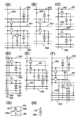
예를 들면, 전극(106)은 전극(101)과 전기적으로 접속할 수 있다. 이와 같이 접속함으로써, 전극(106)에 전극(101)과 같은 전위를 공급할 수 있다. 따라서, 트랜지스터(100)의 온 전류를 늘릴 수 있다. 전극(106)을 전극(101)과 전기적으로 접속한 예를, 도 6(A)∼도 6(E), 도 7(A)∼도 7(E), 도 8(A)∼도 8(E), 도 9(D), 도 9(E), 도 31(A)∼도 31(E), 도 32(A)∼도 32(E), 도 33(A)∼도 33(E), 도 34(D), 도 34(E)에 나타낸다. 또한, 실시형태 1 내지 실시형태 4에 설명한 다양한 도면에 대해서도, 이들 도면과 마찬가지로, 전극(106)과 전극(101)을 전기적으로 접속시킬 수 있고, 마찬가지로 도면을 기술할 수 있다.For example, the
또한, 트랜지스터(100)를 각 화소에 배치하여, 복수의 화소로 이루어지는 화소 매트릭스를 형성하는 경우에, 1 화소마다 개구를 형성하여 전극(106)을 전극(101)과 전기적으로 접속해도 좋다. 그 결과, 콘택트 저항이나 배선 저항을 낮게 할 수 있다. 또는, 복수의 화소마다 개구를 형성하여 전극(106)을 전극(101)과 전기적으로 접속해도 좋다. 그 결과, 레이아웃 면적을 작게 할 수 있다. 또는, 전극(106)과 전극(101)의 전기적 접속은 화소 매트릭스 영역 중에서 행하여도 좋고, 화소 매트릭스 영역의 외측에서 행하여도 좋다. 화소 매트릭스 영역의 외측에서 행함으로써, 화소 매트릭스 영역 중에서의 레이아웃 면적을 작게 할 수 있다. 그 결과, 개구율을 향상시킬 수 있다. 또한, 화소 매트릭스 영역의 외측에 구동 회로가 설치되어 있는 경우는, 전극(106)과 전극(101)의 전기적 접속은 구동 회로와 화소 매트릭스 영역 사이의 영역에서 행하는 것이 적합하다.In the case where the
또는, 예를 들면, 전극(106)은, 전극(104a) 또는 전극(104b)과 전기적으로 접속할 수 있다. 이와 같이 접속함으로써, 전극(106)에 전극(104a) 또는 전극(104b)과 같은 전위를 공급할 수 있다. 전극(106)을 전극(104b)과 접속한 예를, 도 13(A)∼도 13(E), 도 14(A)∼도 14(E), 도 15(A)∼도 15(E), 도 38(A)∼도 38(E), 도 39(A)∼도 39(E), 도 40(A)∼도 40(E)에 나타낸다. 또한, 실시형태 1 내지 실시형태 4에 설명한 다양한 도면에 대해서도, 이들 도면과 마찬가지로, 전극(106)과 전극(104a) 또는 전극(104b)을 전기적으로 접속시킬 수 있고, 마찬가지로 도면을 기술할 수 있다.Alternatively, for example, the
또한, 트랜지스터(100)를 각 화소에 배치하여, 복수의 화소로 이루어지는 화소 매트릭스를 형성하는 경우에, 1 화소마다 개구를 형성하여 전극(106)을 전극(104b)과 전기적으로 접속해도 좋고, 복수의 화소마다 개구를 형성하여 전극(106)을 전극(104b)과 전기적으로 접속해도 좋다. 또한, 전극(106)과 전극(104b)의 전기적 접속은 화소 매트릭스 영역 중에서 행하여도 좋고, 화소 매트릭스 영역의 외측에서 행하여도 좋다. 이것들에 의해, 상술한 경우와 마찬가지로, 콘택트 저항이나 배선 저항을 낮게, 및/또는 레이아웃 면적을 작게 할 수 있다.In addition, when the
또한, 예를 들면, 전극(106)은 전극(104b) 및 전극(110)과 전기적으로 접속할 수 있다. 이와 같이 접속시킴으로써, 전극(106)에 전극(104b) 및 전극(110)과 같은 전위를 공급할 수 있다. 전극(106)을 전극(104b) 및 전극(110)과 접속한 예를, 도 16(A)∼도 16(E), 도 17(A)∼도 17(E), 도 18(A)∼도 18(E), 도 41(A)∼도 41(E), 도 42(A)∼도 42(E), 도 43(A)∼도 43(E)에 나타낸다. 또한, 이들 도면에 나타낸 구성은 전극(110)과 전극(106)이 같은 도전막으로 일체로 형성되는 예이며, 전극(110)과 전극(106)을 총괄하여 전극(110)이라고 표기한다. 또한, 전극(110)과 전극(106)이 같은 도전막으로 형성되는 예를 나타냈지만 이것에 한정되지 않는다. 전극(110)과 전극(106)은 다른 도전막을 에칭 가공함으로써 형성해도 좋다. 또한, 전극(110)과 전극(106)이 접함으로써 전기적으로 접속되어 있어도 좋다. 또한, 실시형태 1 내지 실시형태 4에 설명한 다양한 도면에 대해서도, 이들 도면과 마찬가지로, 전극(106)과 전극(104b) 및 전극(110)을 전기적으로 접속시킬 수 있어, 마찬가지로 도면을 기술할 수 있다.Also, for example,
또한, 예를 들면, 전극(106)은 전극(101)과 같은 층을 이용하여 형성된 전극(101a)과 전기적으로 접속할 수 있다. 여기서, 전극(101)과 전극(101a)은 같은 도전막을 같은 마스크(레티클)를 이용하여 에칭함으로써 형성할 수 있다. 즉, 동시에 패터닝된다. 따라서, 전극(101)과 전극(101a)은 재질, 두께 등은 대체로 동일하다. 전극(106)을 전극(101a)과 접속한 예를, 도 10(A)∼도 10(E), 도 11(A)∼도 11(E), 도 12(A)∼도 12(E), 도 35(A)∼도 35(E), 도 36(A)∼도 36(E), 도 37(A)∼도 37(E)에 나타낸다. 또한, 실시형태 1 내지 실시형태 4에 설명한 다양한 도면에 대해서도, 이들 도면과 마찬가지로, 전극(106)과 전극(101)과 같은 층을 이용하여 형성된 전극을 전기적으로 접속시킬 수 있어, 마찬가지로 도면을 기술할 수 있다.Also, for example, the
또한, 트랜지스터(100)를 각 화소에 배치하여, 복수의 화소로 이루어지는 화소 매트릭스를 형성하는 경우에, 1 화소마다 개구를 형성하여 전극(106)을 전극(101a)과 전기적으로 접속해도 좋고, 복수의 화소마다 개구를 형성하여 전극(106)을 전극(101a)과 전기적으로 접속해도 좋다. 또한, 전극(106)과 전극(101a)의 전기적 접속은 화소 매트릭스 영역 중에서 행하여도 좋고, 화소 매트릭스 영역의 외측에서 행하여도 좋다. 예를 들면, 전극(101a)은 화소 매트릭스에 배치된 용량선으로 할 수 있다. 용량선은 그 외의 배선, 전극, 도전층 등과 절연층을 통하여 중첩되는 것에 의해, 보유 용량 등의 용량을 형성한다. 또는, 전극(101a)은 다른 화소에 배치된 게이트 신호선, 혹은, 같은 화소 중의 다른 게이트 신호선으로 할 수 있다.Further, when the
또한, 예를 들면, 전극(106)은 전극(104a)이나 전극(104b)과 같은 층을 이용하여 형성된 전극(104c)과 전기적으로 접속할 수 있다. 여기서, 전극(104a)과 전극(104b)과 전극(104c)은 같은 도전막을 같은 마스크(레티클)를 이용하여 에칭함으로써 형성할 수 있다. 즉, 동시에 패터닝된다. 따라서, 전극(104a)과 전극(104b)과 전극(104c)은 재질, 두께 등은 대체로 동일하다. 전극(106)을 전극(104c)과 접속한 예를 도 23(A)∼도 23(E), 도 24(A)∼도 24(E), 도 25(A)∼도 25(E), 도 49(A)∼도 49(E), 도 50(A)∼도 50(E), 도 51(A)∼도 51(E)에 나타낸다. 또한, 도 25(A)∼도 25(E), 도 51(A)∼도 51(E)에서, 전극(104c) 아래에는, 반도체층(103)과 같은 층에 형성된 반도체층(103a)이 존재한다. 또한, 실시형태 1 내지 실시형태 4에 설명한 다양한 도면에 대해서도, 이들 도면과 마찬가지로, 전극(106)과 전극(104a)이나 전극(104b)과 같은 층을 이용하여 형성된 전극을 전기적으로 접속시킬 수 있어, 마찬가지로 도면을 기술할 수 있다.Also, for example, the
또한, 트랜지스터(100)를 각 화소에 배치하여, 복수의 화소로 이루어지는 화소 매트릭스를 형성하는 경우에, 1 화소마다 개구를 형성하여 전극(106)을 전극(104c)과 전기적으로 접속해도 좋고, 복수의 화소마다 개구를 형성하여 전극(106)을 전극(104c)과 전기적으로 접속해도 좋다. 또한, 전극(106)과 전극(104c)의 전기적 접속은 화소 매트릭스 영역 중에서 행하여도 좋고, 화소 매트릭스 영역의 외측에서 행하여도 좋다. 예를 들면, 전극(104c)은 화소 매트릭스에 배치된 용량선으로 할 수 있다. 용량선은 그 외의 배선, 전극, 도전층 등과 절연층을 통하여 중첩됨으로써, 보유 용량 등의 용량을 형성한다. 또는, 전극(104c)은 다른 화소에 배치된 신호선, 전원선, 혹은, 같은 화소 중의 다른 신호선, 전원선으로 할 수 있다.In addition, when the
여기서, 전극(101a)이나 전극(104c)을 용량선으로 하는 경우에, 이하의 구성을 적용할 수 있다.Here, when the
화소 매트릭스의 각 화소행(또는 각 화소열)에 용량선을 설치하고, 각 화소행(또는 각 화소열)의 트랜지스터(100)의 전극(106)이 이 화소행(또는 이 화소열)에 설치된 용량선에 전기적으로 접속된 구성으로 해도 좋다. 또는, 화소 매트릭스의 각 화소행(또는 각 화소열)에 용량선을 제공하여, 각 화소행(또는 각 화소열)의 트랜지스터(100)의 전극(106)이 이 화소행(또는 이 화소열) 근처의 화소행(또는 화소열)에 설치된 용량선에 전기적으로 접속된 구성으로 해도 좋다.A capacitor line is provided in each pixel row (or each pixel column) of the pixel matrix, and the
또한, 화소 매트릭스의 1 화소가 복수의 서브 화소를 가지는 경우에는, 각 서브 화소행(또는 각 서브 화소열)에 용량선을 제공하여, 각 서브 화소행(또는 각 서브 화소열)의 트랜지스터(100)의 전극(106)이 이 서브 화소행(또는 이 서브 화소열)에 설치된 용량선에 전기적으로 접속된 구성으로 해도 좋다. 또는, 화소 매트릭스의 1 화소가 복수의 서브 화소를 가지는 경우에는, 각 화소행(또는 각 화소열)에 용량선을 설치하여, 각 서브 화소행(또는 각 서브 화소열)의 트랜지스터(100)의 전극(106)이 이 화소행(또는 이 화소열)에 설치된 용량선에 전기적으로 접속된 구성으로 해도 좋다. 또는, 화소 매트릭스의 1 화소가 복수의 서브 화소를 가지는 경우에는, 각 서브 화소행(또는 각 서브 화소열)에 용량선을 설치하여, 각 서브 화소행(또는 각 서브 화소열)의 트랜지스터(100)의 전극(106)이 이 서브 화소행(또는 이 서브 화소열) 근처의 서브 화소행(또는 서브 화소열)에 설치된 용량선에 전기적으로 접속된 구성으로 해도 좋다.Further, when one pixel of the pixel matrix has a plurality of sub-pixels, a capacitor line is provided in each sub-pixel row (or each sub-pixel column), and the
복수의 용량선은 서로 공유할 수도 있다. 예를 들면, 서로 인접하는 화소(또는 서브 화소)에서 용량선을 공유할 수 있다. 그 결과, 용량선의 수를 줄일 수 있다.A plurality of capacitance lines may be shared with each other. For example, a capacitor line may be shared by pixels (or sub-pixels) adjacent to each other. As a result, the number of capacitance lines can be reduced.
또한, 트랜지스터(100)의 전극(106)이 용량선과 전기적으로 접속되는 경우에, 용량선에 일정한 전위(바람직하게는, 전극(101)에 부여된 전위 중 가장 낮은 전위와 동일한 전위, 또는, 그것보다 더욱 낮은 전위)을 부여할 수 있다. 이것에 의해, 트랜지스터(100)의 스레숄드 전압을 제어하여, 노멀리 오프로 할 수도 있다. 또한, 전극(101), 전극(104a) 등과의 용량 커플링에 기인한 노이즈가 전극(110)에 들어가지 않게 할 수 있다.Further, when the
또한, 트랜지스터(100)의 전극(106)이 용량선과 전기적으로 접속되는 경우에, 용량선에 펄스 신호를 공급할 수 있다. 예를 들면, 코먼 반전 구동을 행하는 경우, 대향 전극과 용량선의 전위가 같은 진폭값으로 변화하는 경우가 있다. 그러한 경우에도, 전극(106)에 트랜지스터(100)가 오프 상태가 되는 낮은 전위를 공급함으로써, 트랜지스터(100)의 스레숄드 전압을 제어하여, 노멀리 오프로 할 수도 있다.Further, when the
또한, 트랜지스터(100)의 전극(106)이 용량선과 전기적으로 접속되는 경우에, 이 용량선을 한쪽의 전극으로서 형성되는 용량 소자의 한쌍의 전극간에는 반도체층(103)을 사이에 두지 않는 것이 바람직하다. 단, 본 발명의 실시형태의 일 양태는 이것에 한정되지 않는다.In the case where the
또한, 전극(101a)이나 전극(104c)은 용량선에 한정되지 않고, 다른 배선으로 할 수 있다. 예를 들면, 전원선, 초기화용 배선 등으로 할 수 있다. 예를 들면, EL 소자(유기 발광 소자)를 이용한 표시 장치에서의 화소 회로에 설치되는 배선이어도 좋다. 또는, 구동 회로(예를 들면, 표시 장치에서의 주사선 구동 회로나 신호선 구동 회로 등)에 설치되는 배선이어도 좋다.In addition, the
본 실시형태는 실시형태 1 내지 실시형태 4의 일부 또는 전부에 대하여, 변경, 추가, 수정, 삭제, 응용, 상위 개념화, 또는, 하위 개념화한 것에 상당한다. 따라서, 실시형태 1 내지 실시형태 4 등의 다른 실시형태와 자유롭게 조합하여 실시할 수 있다.This embodiment corresponds to a change, addition, correction, deletion, application, super-conceptualization, or sub-conceptualization of some or all of the first to fourth embodiments. Therefore, it can be carried out freely in combination with other embodiments such as
(실시형태 6)(Embodiment 6)
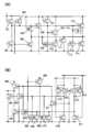
본 실시형태에서는 트랜지스터(100)의 전극(101)(또는 전극(101)과 같은 층에 형성된 전극)과, 트랜지스터(100)의 전극(104a) 또는 전극(104b)(또는 전극(104a)이나 전극(104b)과 같은 층에 형성된 전극)과의 전기적인 접속의 일례에 대하여 설명한다. 설명에는 도 19, 도 44, 도 45를 이용한다. 또한, 설명에 이용하는 도면에서, 앞의 실시형태에서 설명에 이용한 도면과 같은 부분은 같은 부호를 이용하여 나타내고, 설명은 생략한다.In the present embodiment, the
도 19에서는 절연층(105)으로서 층(105a) 및 층(105b)을 형성하는 경우에, 트랜지스터(100)의 전극(101)과 같은 층에 형성된 전극(101a)과, 전극(104a)이나 전극(104b)과 같은 층에 형성된 전극(104c)의 전기적인 접속의 예를 나타낸다.In FIG. 19 , in the case of forming the
도 19(A)에 나타낸 구성에서는, 전극(104c)과 전극(101a)은 층(105a)과 층(105b)에 형성된 개구(191)와, 절연층(102)과 층(105a)과 층(105b)에 형성된 개구(192)에서, 전극(110b)에 의해 전기적으로 접속되어 있다.In the configuration shown in Fig. 19A, the
도 19(B)에 나타낸 구성에서는, 전극(104c)과 전극(101a)은 층(105a)에 형성된 개구(193)와, 절연층(102)과 층(105a)에 형성된 개구(194)에서, 전극(110b)에 의해 전기적으로 접속되어 있다. 즉, 전극(104c)과 전극(101a)의 접속 부분(109)에서 층(105b)은 제거되어 있다.In the configuration shown in FIG. 19(B) , the
또한, 전극(104c)과 전극(101a)의 접속 부분의 전체에서, 층(105b)을 제거하는 구성에 한정되지 않는다. 예를 들면, 도 19(C)나 도 19(D)에 나타낸 구성과 같이, 전극(104c)과 전극(101a)의 접속 부분(109)의 일부에서 층(105b)이 남아 있어도 좋다.In addition, it is not limited to the structure which removes the
도 19(C)에 나타낸 구성에서는, 전극(104c)과 전극(101a)은 층(105a)에 형성된 개구(195)와, 절연층(102)과 층(105a)과 층(105b)에 형성된 개구(196)에서, 전극(110b)에 의해 전기적으로 접속되어 있다.In the configuration shown in Fig. 19C, the
도 19(D)에 나타낸 구성에서는, 전극(104c)과 전극(101a)은 층(105a)과 층(105b)에 형성된 개구(197)와, 절연층(102)과 층(105a)에 형성된 개구(198)에서, 전극(110b)에 의해 전기적으로 접속되어 있다.In the configuration shown in Fig. 19D, the
다음에, 도 44에서는 절연층(105)으로서 층(105b) 및 층(105c)을 형성하는 경우에, 트랜지스터(100)의 전극(101)과 같은 층에 형성된 전극(101a)과, 전극(104a)이나 전극(104b)과 같은 층에 형성된 전극(104c)의 전기적인 접속의 예를 나타낸다.Next, in FIG. 44 , in the case of forming the
도 44(A)에 나타낸 구성에서는, 전극(104c)과 전극(101a)은 층(105b)과 층(105c)에 형성된 개구(441)와, 절연층(102)과 층(105b)과 층(105c)에 형성된 개구(442)에서, 전극(110b)에 의해 전기적으로 접속되어 있다.In the configuration shown in Fig. 44(A), the
도 44(B)에 나타낸 구성에서는, 전극(104c)과 전극(101a)은 층(105c)에 형성된 개구(443)와, 절연층(102)과 층(105c)에 형성된 개구(444)에서, 전극(110b)에 의해 전기적으로 접속되어 있다. 즉, 전극(104c)과 전극(101a)의 접속 부분(109)에서 층(105b)은 제거되어 있다.In the configuration shown in FIG. 44B, the
또한, 전극(104c)과 전극(101a)의 접속 부분의 전체에서 층(105b)을 제거하는 구성에 한정되지 않는다. 예를 들면, 도 44(C)나 도 44(D)에 나타낸 구성과 같이, 전극(104c)과 전극(101a)의 접속 부분(109)의 일부에서 층(105b)이 남아 있어도 좋다.Moreover, it is not limited to the structure which removes the
도 44(C)에 나타낸 구성에서는, 전극(104c)과 전극(101a)은 층(105c)에 형성된 개구(445)와, 절연층(102)과 층(105b)과 층(105c)에 형성된 개구(446)에서, 전극(110b)에 의해 전기적으로 접속되어 있다.In the configuration shown in Fig. 44(C), the
도 44(D)에 나타낸 구성에서는, 전극(104c)과 전극(101a)은 층(105b)과 층(105c)에 형성된 개구(447)와, 절연층(102)과 층(105c)에 형성된 개구(448)에서, 전극(110b)에 의해 전기적으로 접속되어 있다.In the configuration shown in FIG. 44D, the
다음에, 도 45에서는 절연층(105)으로서 층(105a), 층(105b) 및 층(105c)을 형성하는 경우에, 트랜지스터(100)의 전극(101)과 같은 층에 형성된 전극(101a)과, 전극(104a)이나 전극(104b)과 같은 층에 형성된 전극(104c)의 전기적인 접속의 예를 나타낸다.Next, in FIG. 45, in the case of forming the
도 45(A)에 나타낸 구성에서는, 전극(104c)과 전극(101a)은 층(105a)과 층(105b)과 층(105c)에 형성된 개구(451)와, 절연층(102)과 층(105a)과 층(105b)과 층(105c)에 형성된 개구(452)에서, 전극(110b)에 의해 전기적으로 접속되어 있다.In the configuration shown in Fig. 45A, the
도 45(B)에 나타낸 구성에서는, 전극(104c)과 전극(101a)은 층(105a)과 층(105c)에 형성된 개구(453)와, 절연층(102)과 층(105a)과 층(105c)에 형성된 개구(454)에서, 전극(110b)에 의해 전기적으로 접속되어 있다. 즉, 전극(104c)과 전극(101a)의 접속 부분(109)에서 층(105b)은 제거되어 있다.In the configuration shown in Fig. 45B, the
또한, 전극(104c)과 전극(101a)의 접속 부분의 전체에서 층(105b)을 제거하는 구성에 한정되지 않는다. 예를 들면, 도 45(C)나 도 45(D)에 나타낸 구성과 같이, 전극(104c)과 전극(101a)의 접속 부분(109)의 일부에서 층(105b)이 남아 있어도 좋다.Moreover, it is not limited to the structure which removes the
도 45(C)에 나타낸 구성에서는, 전극(104c)과 전극(101a)은 층(105a)과 층(105c)에 형성된 개구(455)와, 절연층(102)과 층(105a)과 층(105b)과 층(105c)에 형성된 개구(456)에서, 전극(110b)에 의해 전기적으로 접속되어 있다.In the configuration shown in FIG. 45(C) , the
도 45(D)에 나타낸 구성에서는, 전극(104c)과 전극(101a)은 층(105a)과 층(105b)과 층(105c)에 형성된 개구(457)와, 절연층(102)과 층(105a)과 층(105c)에 형성된 개구(458)에서, 전극(110b)에 의해 전기적으로 접속되어 있다.In the configuration shown in Fig. 45(D), the
본 실시형태에서 나타낸 전극(104c)과 전극(101a)의 접속 구성은 예를 들면 트랜지스터(100)를 다이오드 접속하는 경우의, 전극(104b)과 전극(101)의 접속 구성에 적용할 수 있다. 다이오드 접속한 트랜지스터는 예를 들면, 보호 회로나, 구동 회로 등에 이용할 수 있다. 또는, 전극(104c)과 전극(101a)의 접속 구성은 게이트 전극과, 소스 전극 또는 드레인 전극을 접속하는 경우에도 적용할 수 있다. 예를 들면, 하나의 화소 중에, 복수의 트랜지스터를 설치하여 구성되는 화소 회로나 구동 회로에서, 게이트 전극과, 소스 전극 또는 드레인 전극을 접속하는 경우에 이용된다. 예를 들면, 화소에 EL 소자(유기 발광 소자)를 가지는 화소 회로에서는 복수의 트랜지스터가 설치되어 있고, 게이트 전극과 소스 전극 또는 드레인 전극을 접속하는 경우가 있다. 또는, 게이트선을 구동하기 위한 회로에서도 복수의 트랜지스터가 설치되어 있다.The connection structure of the
또한, 도 19 중의 개구(191)∼개구(198), 도 44 중의 개구(441)∼개구(448), 도 45 중의 개구(451)∼개구(458)의 형상은 실시형태 4에서 도 4, 도 5, 도 29, 및 도 30을 이용하여 나타낸 개구의 구성과 같은 구성을 적용할 수 있다.In addition, the shapes of the opening 191 - the
또한, 전극(104c)과 전극(101a)과의 접속 구성으로서 전극(110b)을 이용하지 않고 접속시키는 것도 가능하다. 예를 들면, 절연층(102)에 콘택트홀을 형성하여, 전극(104c)과 전극(101a)을 직접 접속시키는 것도 가능하다.It is also possible to connect the
본 실시형태는 실시형태 1 내지 실시형태 5의 일부 또는 전부에 대하여, 변경, 추가, 수정, 삭제, 응용, 상위 개념화, 또는, 하위 개념화한 것에 상당한다. 따라서, 실시형태 1 내지 실시형태 5 등의 다른 실시형태와 자유롭게 조합하여 실시할 수 있다.This embodiment corresponds to a change, addition, correction, deletion, application, higher-level conceptualization, or lower-level conceptualization of some or all of the first to fifth embodiments. Therefore, it can be carried out freely in combination with other embodiments such as
(실시형태 7)(Embodiment 7)
본 실시형태에서는 트랜지스터(100)가 가지는 기생 용량을 크게 하는 구성, 또는, 트랜지스터(100)와 전기적으로 접속되는 용량 소자의 용량값을 크게 하는 구성에 대하여, 그 일례를 설명한다. 설명에는 도 20, 도 21, 도 46, 도 47을 이용한다. 또한, 설명에 이용하는 도면에서, 앞의 실시형태에서 설명에 이용한 도면과 같은 부분은 같은 부호를 이용하여 나타내고, 설명은 생략한다.In the present embodiment, an example of a configuration in which the parasitic capacitance of the
또한, 도 20(A)∼도 20(D) 및 도 21(A)∼도 21(D)은 절연층(105)으로서 층(105a)과 층(105b)의 적층을 이용한 경우의 예이며, 도 46(A), 도 46(C), 도 47(B), 도 47(C)은 절연층(105)으로서 층(105b)과 층(105c)의 적층을 이용한 경우의 예이며, 도 46(B), 도 46(D), 도 47(A), 도 47(D)은 절연층(105)으로서 층(105a)과 층(105b)과 층(105c)의 적층을 이용한 경우의 예이다.20(A) to 20(D) and 21(A) to 21(D) are examples of the case where the
도 20, 도 21, 도 46, 도 47에서는 전극(104b) 위의 층(105b)은 모두, 또는 대부분이 제거되어 있고, 전극(104b)과 전극(106) 사이의 기생 용량의 용량값(또는 용량 소자의 용량값)이 크다. 도면 중, 예를 들면, 파선으로 둘러싸인 부분(281)에서 기생 용량이 생기거나 및/또는 용량 소자가 형성된다. 전극(104b), 전극(106)의 형상이나, 전극(104b) 위의 층(105b)을 제거하는 범위 등을 적절히 정함으로써, 이 용량의 값을 조정할 수 있다.20, 21, 46, and 47, all or most of the
또한, 도 20, 도 21, 도 46, 도 47에서는, 전극(104b)과 전극(101)의 사이에서도 기생 용량이 생기거나 및/또는 용량 소자가 형성될 가능성이 있다. 전극(104b), 전극(101)의 형상을 적절히 정함으로써, 이 용량의 값을 조정할 수 있다.In addition, in FIGS. 20, 21, 46, and 47, there is a possibility that a parasitic capacitance and/or a capacitor may be formed between the
이렇게 하여, 트랜지스터(100)의 게이트와 소스간의 용량을 크게 할 수 있다. 또는, 용량값이 큰 용량 소자를 형성할 수 있다. 예를 들면, 트랜지스터(100)를 부트스트랩 동작을 행하는 회로에 이용하는 경우에는, 게이트와 소스간의 용량을 크게 하는 것이 바람직하다. 또는, 다이나믹 회로에 있어서, 신호를 용량 소자에 보존하는 경우는 그 용량 소자는 큰 것이 바람직하다. 따라서, 도 20, 도 21, 도 46, 도 47 등에 나타낸 구성의 트랜지스터(100)를 이용하는 것이 바람직하다.In this way, the capacitance between the gate and the source of the
본 실시형태는 실시형태 1 내지 실시형태 6의 일부 또는 전부에 대하여, 변경, 추가, 수정, 삭제, 응용, 상위 개념화, 또는, 하위 개념화한 것에 상당한다. 따라서, 실시형태 1 내지 실시형태 6 등의 다른 실시형태와 자유롭게 조합하여 실시할 수 있다.This embodiment corresponds to a change, addition, correction, deletion, application, high-level conceptualization, or low-level conceptualization of some or all of the first to sixth embodiments. Therefore, it can be carried out freely in combination with other embodiments such as
(실시형태 8)(Embodiment 8)
본 실시형태에서는, 반도체 장치 등(표시 장치, 발광 장치 등)이 가지는 용량 소자의 구성에 대하여, 그 일례를 설명한다. 설명에는, 도 22, 도 48을 이용한다. 또한, 설명에 이용하는 도면에서, 앞의 실시형태에서 설명에 이용한 도면과 같은 부분은 같은 부호를 이용하여 나타내고, 설명은 생략한다.In the present embodiment, an example of the configuration of a capacitor included in a semiconductor device or the like (a display device, a light emitting device, etc.) will be described. 22 and 48 are used for the explanation. In addition, in the drawing used for description, the same part as the drawing used for description in the previous embodiment is shown using the same code|symbol, and description is abbreviate|omitted.
또한, 도 22(A)∼도 22(E)에서는 절연층(105)으로서 층(105a)과 층(105b)의 적층을 이용한 경우의 예이며, 도 48(A), 도 48(C)은 절연층(105)으로서 층(105b)과 층(105c)의 적층을 이용한 경우의 예이며, 도 48(B), 도 48(D), 도 48(E)은 절연층(105)으로서 층(105a)과 층(105b)과 층(105c)의 적층을 이용한 경우의 예이다.22(A) to 22(E) are examples of a case in which a stack of
전극(101)과 같은 층에 형성된 전극(101a)을 한쪽의 전극으로 하고, 전극(104a)이나 전극(104b)과 같은 층에 형성된 전극(104c)을 다른 한쪽의 전극으로 하여, 용량 소자를 형성할 수 있다. 이 일례를, 도 22(A), 도 22(B)에 나타낸다. 도면 중, 예를 들면, 파선으로 둘러싸인 부분(282)에 용량 소자는 형성된다. 또한, 전극(106a)은 전극(106)과 같은 층에 형성된 전극이다. 또한, 도 22(A), 도 22(B)에서, 전극(106a)이 전극(104c)과 전기적으로 접속되어 있는 예를 나타냈지만, 본 발명의 실시형태의 일 양태는 이것에 한정되지 않는다. 전극(106a)은 전극(104c)과 전기적으로 접속되어 있지 않아도 좋고, 전극(101a)과 전기적으로 접속되어 있어도 좋고, 전극(101a) 및 전극(104c)의 양쪽 모두와 전기적으로 접속되어 있어도 좋고, 부분(282) 위에 형성하지 않는 구성이어도 좋다.A capacitor is formed by using the
전극(101)과 같은 층에 형성된 전극(101a)을 한쪽의 전극으로 하고, 전극(106a)을 다른 한쪽의 전극으로 하여 용량 소자를 형성할 수 있다. 이 일례를 도 22(C), 도 22(D), 도 22(E), 도 48(A), 도 48(B), 도 48(C), 도 48(D), 도 48(E)에 나타낸다. 도면 중, 예를 들면, 파선으로 둘러싸인 부분(283)에 용량 소자가 형성된다.A capacitor can be formed by using the
또한, 도 22(C)에서 층(105b)의 일부를 제거한 구성이 도 22(D)이다. 도 22(D)에 나타낸 구성에서, 영역(121c)의 층(105b)은 제거되어 있다. 또한, 도 22(D)에서 전극(101a)이 설치된 폭(지면 좌우의 방향)보다 넓은 폭으로 층(105b)을 제거한 구성이 도 22(E)이다. 또한, 도 48(C) 및 도 48(D)에서는 도 48(A), 도 48(B)에서, 층(105b)의 일부를 제거한 구성을 나타내고 있다. 도 48(C) 및 도 48(D)에 나타낸 구성에서, 영역(121c)의 층(105b)은 제거되어 있다. 또한, 도 48(D)에서 전극(101a)이 설치된 폭(지면 좌우의 방향)보다 넓은 폭으로 층(105b)을 제거한 구성이 도 48(E)이다.22(D) is a configuration in which a part of the
또한, 도 22, 도 48에서, 전극(106a)은 전극(106)이나 전극(110)이나 전극(110)과 같은 층에 형성되는 전극이어도 좋다. 전극(101a)은 전극(101)이어도 좋다. 전극(104c)은 전극(104)이어도 좋다.22 and 48 , the
도 22나 도 48에 나타낸 용량 소자는 트랜지스터(100)의 게이트와 소스 사이에 설치되는 용량 소자로서 이용할 수 있다. 또는, 예를 들면, 화소에 설치되는 보유 용량으로서 이용할 수 있다. 또는, 구동 회로에서, 신호를 보유하기 위한 용량 소자로서 이용할 수 있다.The capacitor shown in FIG. 22 or FIG. 48 can be used as a capacitor provided between the gate and the source of the
본 실시형태는 실시형태 1 내지 실시형태 7의 일부 또는 전부에 대하여, 변경, 추가, 수정, 삭제, 응용, 상위 개념화, 또는, 하위 개념화한 것에 상당한다. 따라서, 실시형태 1 내지 실시형태 7 등의 다른 실시형태와 자유롭게 조합하여 실시할 수 있다.This embodiment corresponds to a change, addition, correction, deletion, application, super-conceptualization, or sub-conceptualization of some or all of
(실시형태 9)(Embodiment 9)
본 실시형태에서는, 실시형태 1 내지 실시형태 8에서 나타낸 구성에서의 절연층, 전극, 반도체층 등의 재료의 일례에 대하여 설명한다.In this embodiment, an example of materials, such as an insulating layer, an electrode, a semiconductor layer, in the structure shown in Embodiment 1-8 is demonstrated.
트랜지스터(100)의 반도체층(103)의 재료에 대하여 이하에 설명한다. 또한, 반도체층(103)과 같은 층에 형성하는 반도체층도 같은 재료를 이용할 수 있다.The material of the
트랜지스터(100)의 반도체층(103)은 산화물 반도체로 이루어지는 층(산화물 반도체층)를 포함해도 좋다. 산화물 반도체로서는, 예를 들면, 4원계 금속의 산화물인 In-Sn-Ga-Zn-O계 산화물 반도체나, 3원계 금속의 산화물인 In-Ga-Zn-O계 산화물 반도체, In-Sn-Zn-O계 산화물 반도체, In-Al-Zn-O계 산화물 반도체, Sn-Ga-Zn-O계 산화물 반도체, Al-Ga-Zn-O계 산화물 반도체, Sn-Al-Zn-O계 산화물 반도체, Hf-In-Zn-O계 산화물 반도체나, 2원계 금속의 산화물인 In-Zn-O계 산화물 반도체, Sn-Zn-O계 산화물 반도체, Al-Zn-O계 산화물 반도체, Zn-Mg-O계 산화물 반도체, Sn-Mg-O계 산화물 반도체, In-Mg-O계 산화물 반도체나, In-Ga-O계 산화물 반도체, 1원계 금속의 산화물인 In-O계 산화물 반도체, Sn-O계 산화물 반도체, Zn-O계 산화물 반도체 등을 이용할 수 있다. 또한, 상기 산화물 반도체에 In과 Ga와 Sn과 Zn 이외의 원소, 예를 들면 SiO2를 포함시켜도 좋다.The
예를 들면, In-Sn-Zn-O계 산화물 반도체란, 인듐(In), 주석(Sn), 아연(Zn)을 가지는 산화물 반도체라는 의미이며, 그 조성비는 묻지 않는다. 또 예를 들면, In-Ga-Zn-O계 산화물 반도체란, 인듐(In), 갈륨(Ga), 아연(Zn)을 가지는 산화물 반도체라는 의미이며, 그 조성비는 묻지 않는다. In-Ga-Zn-O계 산화물 반도체는 IGZO라고 부를 수 있다.For example, the In-Sn-Zn-O-based oxide semiconductor means an oxide semiconductor containing indium (In), tin (Sn), and zinc (Zn), and the composition ratio is not questioned. Moreover, for example, an In-Ga-Zn-O type|system|group oxide semiconductor means an oxide semiconductor which has indium (In), gallium (Ga), and zinc (Zn), The composition ratio does not matter. The In-Ga-Zn-O-based oxide semiconductor can be called IGZO.
또한, 산화물 반도체층은 산화물 반도체막을 이용하여 형성할 수 있다. In-Sn-Zn-O계 산화물 반도체막을 스퍼터링법에 의해 형성하는 경우, 타겟의 조성비는 원자수비로 In:Sn:Zn이 1:2:2, 2:1:3, 1:1:1, 또는 20:45:35 등을 이용한다.In addition, the oxide semiconductor layer can be formed using an oxide semiconductor film. When an In-Sn-Zn-O-based oxide semiconductor film is formed by sputtering, the composition ratio of the target is In:Sn:Zn 1:2:2, 2:1:3, 1:1:1, Or 20:45:35, etc.
또한, In-Zn-O계 산화물 반도체막을 스퍼터링법에 의해 형성하는 경우, 타겟의 조성비는 원자수비로, In:Zn = 50:1∼1:2(몰수비로 환산하면 In2O3:ZnO = 25:1∼1:4), 바람직하게는 In:Zn = 20:1∼1:1(몰수비로 환산하면 In2O3:ZnO = 10:1∼1:2), 더욱 바람직하게는 In:Zn = 1.5:1∼15:1(몰수비로 환산하면 In2O3:ZnO = 3:4∼15:2)로 한다. 예를 들면, 타겟은 원자수비가 In:Zn:O = X:Y:Z일 때, Z>1.5X+Y로 한다.In addition, when an In-Zn-O-based oxide semiconductor film is formed by sputtering, the composition ratio of the target is in an atomic ratio, In:Zn = 50:1 to 1:2 (In2 O3 :ZnO = in terms of mole ratio) 25:1 to 1:4), preferably In:Zn = 20:1 to 1:1 (in terms of mole ratio, In2 O3 :ZnO = 10:1 to 1:2), more preferably In: Zn = 1.5:1 to 15:1 (In2 O3 :ZnO = 3:4 to 15:2 in terms of mole ratio). For example, the target is Z>1.5X+Y when the atomic ratio is In:Zn:O = X:Y:Z.
또한, In-Ga-Zn-O계 산화물 반도체막을 스퍼터링법에 의해 형성하는 경우, 타겟의 조성비는 원자수비로, In:Ga:Zn = 1:1:0.5, In:Ga:Zn = 1:1:1, 또는 In:Ga:Zn = 1:1:2로 할 수 있다.In addition, when an In-Ga-Zn-O-based oxide semiconductor film is formed by sputtering, the composition ratio of the target is an atomic ratio, In:Ga:Zn = 1:1:0.5, In:Ga:Zn = 1:1 :1, or In:Ga:Zn = 1:1:2.
또한, 타겟의 순도를 99.99% 이상으로 함으로써, 산화물 반도체막에 혼입하는 알칼리 금속, 수소 원자, 수소 분자, 물, 수산기, 또는 수소화물 등을 저감할 수 있다. 또한, 이 타겟을 이용함으로써, 산화물 반도체막에서, 리튬, 나트륨, 칼륨 등의 알칼리 금속의 농도를 저감할 수 있다.In addition, by setting the purity of the target to 99.99% or more, it is possible to reduce alkali metals, hydrogen atoms, hydrogen molecules, water, hydroxyl groups, hydrides, and the like mixed into the oxide semiconductor film. Moreover, by using this target, the density|concentration of alkali metals, such as lithium, sodium, and potassium, in an oxide semiconductor film can be reduced.
또한, 산화물 반도체는 불순물에 대하여 둔감하고, 막 중에는 상당한 금속 불순물이 포함되어 있어도 문제가 없고, 나트륨(Na)과 같은 알칼리 금속이 다량으로 포함되는 저렴한 소다 석회 유리도 사용할 수 있다고 지적되어 있다(카미야, 노무라, 호소노, 「아몰퍼스(amorphous) 산화물 반도체의 물성과 디바이스 개발의 현상(現狀)」, 고체 물리, 2009년 9월호, Vol. 44, pp. 621-633.). 그러나, 이러한 지적은 적절하지 않다. 알칼리 금속은 산화물 반도체를 구성하는 원소는 아니기 때문에 불순물이다. 알칼리토 금속도 산화물 반도체를 구성하는 원소가 아닌 경우에 불순물이 된다. 특히, 알칼리 금속 중 Na는 산화물 반도체층에 접하는 절연막이 산화물인 경우, 이 절연막 중으로 확산하여 Na+가 된다. 또한, Na는 산화물 반도체층 내에서 산화물 반도체를 구성하는 금속과 산소의 결합을 분단하거나, 혹은, 그 결합 중에 끼어든다. 그 결과, 예를 들면, 스레숄드 전압이 마이너스 방향으로 시프트하는 것에 의한 노멀리 온화, 이동도의 저하 등의 트랜지스터의 특성의 열화가 일어나고, 더하여, 특성의 편차도 생긴다. 이 불순물에 의해 초래되는 트랜지스터의 특성의 열화와 특성의 편차는, 산화물 반도체층 중의 수소 농도가 충분히 낮은 경우에 현저하게 나타난다. 따라서, 산화물 반도체층 중의 수소 농도가 1×10¹⁸/cm3 이하, 보다 바람직하게는 1×10¹⁷/cm3 이하인 경우에는, 상기 불순물의 농도를 저감하는 것이 바람직하다. 구체적으로, 2차 이온 질량분석법에 의한 Na 농도의 측정값은 5×10¹⁶/cm3 이하, 바람직하게는 1×10¹⁶/cm3 이하, 더욱 바람직하게는 1×10¹⁵/cm3 이하로 하면 좋다. 마찬가지로 Li 농도의 측정값은 5×10¹⁵/cm3 이하, 바람직하게는 1×10¹⁵/cm3 이하로 하면 좋다. 마찬가지로, K 농도의 측정값은 5×10¹⁵/cm3 이하, 바람직하게는 1×10¹⁵/cm3 이하로 하면 좋다.In addition, it is pointed out that oxide semiconductors are insensitive to impurities, and there is no problem even if significant metal impurities are contained in the film, and inexpensive soda-lime glass containing a large amount of alkali metals such as sodium (Na) can be used (Kamiya) , Nomura, Hosono, “Physical properties of amorphous oxide semiconductors and the current status of device development,” Solid State Physics, September 2009, Vol. 44, pp. 621-633.). However, this point is not appropriate. Alkali metal is an impurity because it is not an element constituting an oxide semiconductor. Alkaline earth metal also becomes an impurity when it is not an element constituting an oxide semiconductor. In particular, in the alkali metal, when the insulating film in contact with the oxide semiconductor layer is an oxide, Na diffuses into the insulating film to become Na+ . In addition, Na breaks the bond between the metal and oxygen constituting the oxide semiconductor in the oxide semiconductor layer, or intervenes in the bond. As a result, for example, deterioration of the characteristics of the transistor, such as normally warming and a decrease in mobility due to the threshold voltage shifting in the negative direction, occurs, and furthermore, variations in the characteristics occur. The deterioration of the characteristics of the transistor and the variation in characteristics caused by this impurity are remarkably shown when the hydrogen concentration in the oxide semiconductor layer is sufficiently low. Therefore, when the hydrogen concentration in the oxide semiconductor layer is 1×10¹⁸ /cm3 or less, more preferably 1×10¹⁷ /cm3 or less, it is preferable to reduce the concentration of the impurity. Specifically, the measured value of the Na concentration by secondary ion mass spectrometry is 5×10¹⁶ /cm3 or less, preferably 1×10¹⁶ /cm3 or less, more preferably 1×10¹⁵ /cm3 or less. good to do Similarly, the measured value of the Li concentration may be 5×10¹⁵ /cm3 or less, preferably 1×10¹⁵ /cm3 or less. Similarly, the measured value of the K concentration may be 5×10¹⁵ /cm3 or less, preferably 1×10¹⁵ /cm3 or less.
또한 산화물 반도체층은 비정질이어도 좋지만, 결정성을 가지고 있어도 좋다. 산화물 반도체층은 단결정이어도, 비단결정이어도 좋다. 비단결정의 경우, 아몰퍼스이어도, 다결정이어도 좋다. 또한, 아몰퍼스 중에 결정성을 가지는 부분을 포함하는 구조이어도, 비아몰퍼스이어도 좋다. 산화물 반도체층으로서는 c축 배향하고, 그 ab면에 수직인 방향으로부터 볼 때, 삼각형, 육각형, 정삼각형, 또는 정육각형의 원자 배열을 가지고, 또한 c축 방향으로 수직인 방향에서 볼 때, 금속 원자가 층상, 또는 금속 원자와 산소 원자가 층상으로 배열한 상(相)을 포함하는 결정(CAAC:C Axis Aligned Crystal이라고도 함)을 포함하는 산화물을 이용할 수 있다.The oxide semiconductor layer may be amorphous, but may have crystallinity. The oxide semiconductor layer may be a single crystal or a non-single crystal. In the case of a non-single crystal, amorphous or polycrystal may be sufficient. Moreover, the structure containing the part which has crystallinity in an amorphous may be sufficient, or non-morphous may be sufficient. The oxide semiconductor layer is c-axis oriented, has a triangular, hexagonal, equilateral triangle, or regular hexagonal atomic arrangement when viewed from a direction perpendicular to the ab-plane, and when viewed from a direction perpendicular to the c-axis direction, metal atoms are layered, Alternatively, an oxide including a crystal (also referred to as C Axis Aligned Crystal (CAAC)) including a phase in which metal atoms and oxygen atoms are arranged in a layered form may be used.
CAAC에 대하여 도 69 내지 도 71을 이용하여 상세하게 설명한다. 또한, 특별히 언급하지 않는 한, 도 69 내지 도 71은 상방향을 c축 방향으로 하고, c축 방향과 직교하는 면을 ab면으로 한다. 또한, 단지 상반분, 하반분이라고 하는 경우, ab면을 경계로 한 경우의 상반분, 하반분을 말한다. 또한, 도 69에서, 동그라미로 둘러싸인 O원자는 4배위의 O원자를 나타내고, 이중 동그라미로 둘러싸인 O원자는 3배위의 O원자를 나타낸다.CAAC will be described in detail with reference to FIGS. 69 to 71 . In addition, unless otherwise noted, in FIGS. 69 to 71, the upward direction is the c-axis direction, and the plane orthogonal to the c-axis direction is the ab plane. In addition, in the case of only the upper half and the lower half, the upper half and the lower half in the case of using the ab plane as a boundary are referred to. Further, in Fig. 69, an O atom surrounded by a circle represents an O atom with a tetracoordinate, and an O atom surrounded by a double circle represents an O atom with a triple coordination.
도 69(A)에 1개의 6배위의 In 원자와, In 원자에 근접한 6개의 4배위의 산소 원자(이하 4배위의 O원자)를 가지는 구조를 나타낸다. In 원자 하나에 대하여, 근접 산소 원자만 나타낸 구조를, 여기에서는 서브 유닛이라고 부른다. 도 69(A)의 구조는 팔면체 구조를 취하지만, 간단하게 하기 위해 평면 구조로 나타내고 있다. 또한, 도 69(A)의 상반분 및 하반분에는 각각 3개씩 4배위의 O원자가 있다. 도 69(A)에 나타낸 서브 유닛은 전하가 0이다.Fig. 69(A) shows a structure having one hexacoordinated In atom and six tetracoordinated oxygen atoms (hereinafter, tetracoordinated O atoms) adjacent to the In atom. A structure in which only adjacent oxygen atoms are shown with respect to one In atom is called a subunit here. Although the structure in Fig. 69(A) has an octahedral structure, it is shown as a planar structure for simplicity. In addition, in the upper half and the lower half of FIG. 69(A), there are three O atoms in tetracoordinated position, respectively. The subunit shown in Fig. 69(A) has zero charge.
도 69(B)에 1개의 5배위의 Ga 원자와, Ga 원자에 근접한 3개의 3배위의 산소 원자(이하 3배위의 O원자)와, Ga 원자에 근접한 2개의 4배위의 O원자를 가지는 구조를 나타낸다. 3배위의 O원자는 어느 것도 ab면에 존재한다. 도 69(B)의 상반분 및 하반분에는 각각 1개씩 4배위의 O원자가 있다. 또한, In 원자도 5배위를 취하기 때문에, 도 69(B)에 나타낸 구조를 취할 수 있다. 도 69(B)에 나타낸 서브 유닛은 전하가 0이다.69(B) shows a structure having one pentacoordinated Ga atom, three tricoordinated oxygen atoms close to the Ga atom (hereinafter referred to as tricoordinated O atoms), and two tetracoordinated O atoms close to the Ga atom. indicates None of the tricoordinated O atoms are on the ab side. In the upper and lower halves of FIG. 69(B), there are O atoms in tetracoordinate, one each. In addition, since the In atom also takes the pentacoordinate, the structure shown in Fig. 69(B) can be taken. The subunit shown in Fig. 69(B) has zero charge.
도 69(C)에 1개의 4배위의 Zn 원자와, Zn 원자에 근접한 4개의 4배위의 O원자에 의한 구조를 나타낸다. 도 69(C)의 상반분에는 1개의 4배위의 O원자가 있고, 하반분에는 3개의 4배위의 O원자가 있다. 또는, 도 69(C)의 상반분에 3개의 4배위의 O원자가 있고, 하반분에 1개의 4배위의 O원자가 있어도 좋다. 도 69(C)에 나타낸 서브 유닛은 전하가 0이다.Fig. 69(C) shows a structure with one tetracoordinated Zn atom and four tetracoordinated O atoms close to the Zn atom. In the upper half of FIG. 69(C), there is one tetracoordinated O atom, and in the lower half there are three tetracoordinated O atoms. Alternatively, there may be three tetracoordinated O atoms in the upper half of Fig. 69(C) and one tetracoordinated O atom in the lower half. The subunit shown in Fig. 69(C) has zero charge.
도 69(D)에, 1개의 6배위의 Sn 원자와, Sn 원자에 근접한 6개의 4배위의 O원자를 가지는 구조를 나타낸다. 도 69(D)의 상반분에는 3개의 4배위의 O원자가 있고, 하반분에는 3개의 4배위의 O원자가 있다. 도 69(D)에 나타낸 서브 유닛은 전하가 +1이 된다.Fig. 69(D) shows a structure having one hexacoordinated Sn atom and six tetracoordinated O atoms close to the Sn atom. In the upper half of FIG. 69(D), there are three tetracoordinated O atoms, and in the lower half there are three tetracoordinated O atoms. The subunit shown in Fig. 69(D) has a charge of +1.
도 69(E)에 2개의 Zn 원자를 포함하는 서브 유닛을 나타낸다. 도 69(E)의 상반분에는 1개의 4배위의 O원자가 있고, 하반분에는 1개의 4배위의 O원자가 있다. 도 69(E)에 나타낸 서브 유닛은 전하가 ―1이 된다.Fig. 69(E) shows a subunit including two Zn atoms. In the upper half of Fig. 69(E), there is one tetracoordinated O atom, and in the lower half there is one tetracoordinated O atom. The subunit shown in Fig. 69(E) has an electric charge of -1.
여기에서는, 서브 유닛의 몇 개의 집합체를 1 그룹이라고 부르고, 그룹의 몇 개의 집합체를 1 유닛이라고 부른다.Here, some aggregates of subunits are called 1 group, and some aggregates of groups are called 1 unit.
여기서, 이들 서브 유닛들이 결합하는 규칙에 대하여 설명한다. 도 69(A)에 나타낸 6배위의 In 원자의 상반분의 3개의 O원자는 하방향에 각각 3개의 근접 In 원자를 가지고, 하반분의 3개의 O원자는 상방향에 각각 3개의 근접 In 원자를 가진다. 도 69(B)에 나타낸 5배위의 Ga 원자의 상반분의 1개의 O원자는 하방향에 1개의 근접 Ga 원자를 가지고, 하반분의 1개의 O원자는 상방향에 1개의 근접 Ga 원자를 가진다. 도 69(C)에 나타낸 4배위의 Zn 원자의 상반분의 1개의 O원자는 하방향에 1개의 근접 Zn 원자를 가지고, 하반분의 3개의 O원자는 상방향에 각각 3개의 근접 Zn 원자를 가진다. 이와 같이, 금속 원자의 상방향의 4배위의 O원자의 수와, 그 O원자의 하방향에 있는 근접 금속 원자의 수는 동일하고, 마찬가지로 금속 원자의 하방향의 4배위의 O원자의 수와, 그 O원자의 상방향에 있는 근접 금속 원자의 수는 동일하다. O원자는 4배위이므로, 하방향에 있는 근접 금속 원자의 수와, 상방향에 있는 근접 금속 원자의 수의 합은 4가 된다. 따라서, 금속 원자의 상방향에 있는 4배위의 O원자의 수와, 다른 금속 원자의 하방향에 있는 4배위의 O원자의 수와의 합이 4개일 때, 금속 원자를 가지는 2종의 서브 유닛들은 결합할 수 있다. 예를 들면, 6배위의 금속 원자(In 또는 Sn)가 하반분의 4배위의 O원자를 통하여 결합하는 경우, 4배위의 O원자가 3개이기 때문에, 5배위의 금속 원자(Ga 또는 In) 또는 4배위의 금속 원자(Zn)의 어느 하나와 결합하게 된다.Here, the rules for combining these sub-units will be described. The three O atoms in the upper half of the 6-coordinated In atoms shown in Fig. 69(A) each have three adjacent In atoms in the downward direction, and the three O atoms in the lower half each have three adjacent In atoms in the upward direction. have One O atom in the upper half of the pentacoordinate Ga atoms shown in Fig. 69(B) has one adjacent Ga atom in the downward direction, and one O atom in the lower half has one adjacent Ga atom in the upward direction. . One O atom in the upper half of the tetracoordinated Zn atoms shown in FIG. 69(C) has one adjacent Zn atom in the downward direction, and the three O atoms in the lower half have three adjacent Zn atoms in the upward direction. have In this way, the number of O atoms in the tetracoordinate direction of a metal atom is the same as the number of adjacent metal atoms in the downward direction of the O atom, and similarly, the number of O atoms in the tetracoordinate direction of the metal atom is equal to the number of O atoms in the downward direction of the metal atom , the number of adjacent metal atoms upstream of that O atom is the same. Since the O atom is tetracoordinate, the sum of the number of adjacent metal atoms in the downward direction and the number of adjacent metal atoms in the upward direction becomes 4. Therefore, when the sum of the number of tetracoordinated O atoms in the upper direction of a metal atom and the number of tetracoordinated O atoms in the downward direction of another metal atom is 4, two types of subunits having a metal atom can be combined. For example, when a 6-coordinated metal atom (In or Sn) is bonded through an O atom in the tetracoordinate of the lower half, since there are three O atoms in the tetracoordinate, a metal atom (Ga or In) in the 5-coordinated or It is bound to any one of the tetracoordinated metal atoms (Zn).
이러한 배위수를 가지는 금속 원자는 c축 방향에서, 4배위의 O원자를 통하여 결합한다. 또한, 이 밖에도, 층 구조의 합계의 전하가 0이 되도록 서브 유닛들이 결합하여 1 그룹을 구성한다.A metal atom having such a coordination number is bonded in the c-axis direction through a tetracoordinated O atom. In addition, subunits are combined to form one group so that the total charge of the layer structure becomes zero.
도 70(A)에 In-Sn-Zn-O계의 층 구조를 구성하는 1 그룹의 모델도를 나타낸다. 도 70(B)에 3개의 그룹으로 구성되는 유닛을 나타낸다. 또한, 도 70(C)은 도 70(B)의 층 구조를 c축 방향에서 관찰한 경우의 원자 배열을 나타낸다.Fig. 70(A) shows a model diagram of one group constituting the In-Sn-Zn-O-based layer structure. Fig. 70(B) shows a unit composed of three groups. 70(C) shows the atomic arrangement when the layer structure of FIG. 70(B) is observed in the c-axis direction.
도 70(A)에서는, 간단하게 하기 위해, 3배위의 O원자는 생략하고, 4배위의 O원자는 갯수만 나타내고, 예를 들면, Sn 원자의 상반분 및 하반분에는 각각 3개씩 4배위의 O원자가 있는 것을 동그라미 3으로 나타낸다. 마찬가지로, 도 70(A)에서 In 원자의 상반분 및 하반분에는 각각 1개씩 4배위의 O원자가 있고, 동그라미 1로서 나타낸다. 또한, 마찬가지로, 도 70(A)에서 하반분에는 1개의 4배위의 O원자가 있고, 상반분에는 3개의 4배위의 O원자가 있는 Zn 원자와, 상반분에는 1개의 4배위의 O원자가 있고, 하반분에는 3개의 4배위의 O원자가 있는 Zn 원자를 나타낸다.In Fig. 70(A), for the sake of simplicity, the tricoordinate O atom is omitted, and only the number of tetracoordinate O atoms is shown. A circle with an O atom is denoted by
도 70(A)에서, In-Sn-Zn-O계의 층 구조를 구성하는 그룹은 위에서부터 순차로 4배위의 O원자가 3개씩 상반분 및 하반분에 있는 Sn 원자가 4배위의 O원자가 1개씩 상반분 및 하반분에 있는 In 원자와 결합하고, 그 In 원자가 상반분에 3개의 4배위의 O원자가 있는 Zn 원자와 결합하고, 그 Zn 원자의 하반분의 1개의 4배위의 O원자를 통하여 4배위의 O원자가 3개씩 상반분 및 하반분에 있는 In 원자와 결합하고, 그 In 원자가 상반분에 1개의 4배위의 O원자가 있는 Zn 원자 2개로 이루어지는 서브 유닛과 결합하고, 이 서브 유닛의 하반분의 1개의 4배위의 O원자를 통하여 4배위의 O원자가 3개씩 상반분 및 하반분에 있는 Sn 원자와 결합하는 구성이다. 그룹의 몇 개를 결합하여 1 유닛을 구성한다.In Fig. 70(A), the groups constituting the In-Sn-Zn-O-based layer structure have three tetracoordinated O atoms sequentially from the top, and one Sn tetracoordinated O atom in the upper and lower halves. Bonds with In atoms in the upper and lower halves, the In atom bonds to Zn atoms having three tetracoordinated O atoms in the upper halves, and 4 through one tetracoordinated O atom in the lower half of the Zn atom Three O atoms of coordination are bonded to In atoms in the upper and lower halves, and the In atoms are bonded to a subunit composed of two Zn atoms having one tetracoordinated O atom in the upper half, and the lower half of this subunit It is a configuration in which three O atoms of tetracoordination are bonded to Sn atoms in the upper and lower halves through one tetracoordinated O atom. Combine several groups to form 1 unit.
여기서, 3배위의 O원자 및 4배위의 O원자의 경우, 결합 1개 당의 전하는 각각 -0.667, -0.5라고 생각할 수 있다. 예를 들면, In(6배위 또는 5배위) 원자, Zn(4배위) 원자, Sn(5배위 또는 6배위) 원자의 전하는 각각 +3, +2, +4이다. 따라서, Sn 원자를 포함하는 서브 유닛은 전하가 +1이 된다. 따라서, Sn 원자를 포함하는 층 구조를 형성하기 위해서는, 전하 +1을 지우는 전하 ―1이 필요하다. 전하 ―1을 취하는 구조로서 도 69(E)에 나타낸 바와 같이, 2개의 Zn 원자를 포함하는 서브 유닛을 들 수 있다. 예를 들면, Sn 원자를 포함하는 서브 유닛이 1개에 대하여, 2개의 Zn 원자를 포함하는 서브 유닛이 1개 있으면, 전하가 지워지기 때문에, 층 구조의 합계의 전하를 0으로 할 수 있다.Here, in the case of the tricoordinate O atom and the tetracoordinate O atom, it can be considered that the charges per bond are −0.667 and −0.5, respectively. For example, the charges of an In (hexacoordinated or pentacoordinated) atom, a Zn (tetracoordinated) atom, and a Sn (pentacoordinated or hexacoordinated) atom are +3, +2, and +4, respectively. Accordingly, the subunit containing Sn atoms has a charge of +1. Therefore, in order to form a layer structure containing Sn atoms, a charge of -1 that erases the charge of +1 is required. A subunit containing two Zn atoms as shown in Fig. 69(E) is exemplified as a structure having a charge of -1. For example, if there is one subunit containing two Zn atoms for one subunit containing Sn atoms, since the charge is erased, the total charge of the layer structure can be set to zero.
또한, In 원자는 5배위 및 6배위를 모두 취할 수 있는 것으로 한다. 구체적으로는, 도 70(B)에 나타낸 유닛으로 함으로써, In-Sn-Zn-O계의 결정(In2SnZn3O8)을 얻을 수 있다. 또한, 얻어지는 In-Sn-Zn-O계의 층 구조는 In2SnZn2O7(ZnO)m(M은 0또는 자연수)으로 하는 조성식으로 나타낼 수 있다.In addition, it is assumed that the In atom can take both 5-coordinated and 6-coordinated. Specifically, by setting it as the unit shown in FIG. 70(B), an In-Sn-Zn-O-based crystal (In2 SnZn3 O8 ) can be obtained. Further, the layer structure of the SnZn-In-O system obtained may be represented by a composition formula ofIn 2 SnZn 2 O 7 (ZnO ) m (M is 0 or a natural number).
또한, 이 밖에도, 4원계 금속의 산화물인 In-Sn-Ga-Zn-O계 산화물이나, 3원계 금속의 산화물인 In-Ga-Zn-O계 산화물(IGZO와도 표기함), In-Al-Zn-O계 산화물, Sn-Ga-Zn-O계 산화물, Al-Ga-Zn-O계 산화물, Sn-Al-Zn-O계 산화물이나, 2원계 금속의 산화물인 In-Zn-O계 산화물, Sn-Zn-O계 산화물, Al-Zn-O계 산화물, Zn-Mg-O계 산화물, Sn-Mg-O계 산화물, In-Mg-O계 산화물이나, In-Ga-O계 산화물, 1원계 금속의 산화물인 In-O계 산화물, Sn-O계 산화물, Zn-O계 산화물 등을 이용한 경우도 마찬가지이다.In addition, In-Sn-Ga-Zn-O type oxide which is an oxide of a quaternary metal, In-Ga-Zn-O type oxide which is an oxide of a ternary metal (also denoted with IGZO), In-Al- Zn-O-based oxides, Sn-Ga-Zn-O-based oxides, Al-Ga-Zn-O-based oxides, Sn-Al-Zn-O-based oxides, and In-Zn-O-based oxides that are oxides of binary metals , Sn-Zn-O-based oxide, Al-Zn-O-based oxide, Zn-Mg-O-based oxide, Sn-Mg-O-based oxide, In-Mg-O-based oxide, In-Ga-O-based oxide, The same applies to the case where an In-O-based oxide, a Sn-O-based oxide, a Zn-O-based oxide, or the like, which is an oxide of a single-based metal, is used.
예를 들면, 도 71(A)에 In-Ga-Zn-O계의 층 구조를 구성하는 1 그룹의 모델도를 나타낸다.For example, Fig. 71(A) shows a model diagram of one group constituting the In-Ga-Zn-O-based layer structure.
도 71(A)에서 In-Ga-Zn-O계의 층 구조를 구성하는 그룹은 위에서부터 순차로 4배위의 O원자가 3개씩 상반분 및 하반분에 있는 In 원자가, 4배위의 O원자가 1개 상반분에 있는 Zn 원자와 결합하고, 그 Zn 원자의 하반분의 3개의 4배위의 O원자를 통하여, 4배위의 O원자가 1개씩 상반분 및 하반분에 있는 Ga 원자와 결합하고, 그 Ga 원자의 하반분의 1개의 4배위의 O원자를 통하여, 4배위의 O원자가 3개씩 상반분 및 하반분에 있는 In 원자와 결합한 구성이다. 그룹의 몇 개를 결합하여 1 유닛을 구성한다.In Fig. 71(A), the group constituting the In-Ga-Zn-O-based layer structure has three tetracoordinated O atoms sequentially from the top, one In valence in the upper and lower halves, and one tetracoordinate O atom. It bonds to the Zn atom in the upper half, and through the three tetracoordinated O atoms in the lower half of the Zn atom, one tetracoordinate O atom bonds to the Ga atoms in the upper half and the lower half, and the Ga atom Through one tetracoordinated O atom in the lower half of , three O atoms in tetracoordinate are bonded to In atoms in the upper and lower halves. Combine several groups to form 1 unit.
도 71(B)에 3개의 그룹으로 구성되는 유닛을 나타낸다. 또한, 도 71(C)은 도 71(B)의 층 구조를 c축 방향에서 관찰한 경우의 원자 배열을 나타낸다.Fig. 71(B) shows a unit composed of three groups. Fig. 71(C) shows the atomic arrangement when the layer structure of Fig. 71(B) is observed in the c-axis direction.
여기서, In(6배위 또는 5배위) 원자, Zn(4배위) 원자, Ga(5배위) 원자의 전하는 각각 +3, +2, +3이기 때문에, In 원자, Zn 원자 및 Ga 원자로 이루어지는 서브 유닛은 전하가 0이 된다. 따라서, 이러한 조합이면 층 구조의 합계의 전하는 항상 0이 된다.Here, since the charges of In (6-coordinated or 5-coordinated) atoms, Zn (tetracoordinated) atoms, and Ga (pentacoordinated) atoms are +3, +2, and +3, respectively, the subunits composed of In atoms, Zn atoms and Ga atoms have a charge. becomes 0. Therefore, in such a combination, the charge of the sum of the layer structures is always zero.
여기서, In(6배위 또는 5배위) 원자, Zn(4배위) 원자, Ga(5배위) 원자의 전하는 각각 +3, +2, +3이기 때문에, In 원자, Zn 원자 및 Ga 원자의 어느 것을 포함하는 서브 유닛은 전하가 0이 된다. 따라서, 이들 서브 유닛의 조합이면 그룹의 합계의 전하는 항상 0이 된다.Here, since the charges of the In (hexacoordinated or pentacoordinated) atom, the Zn (tetracoordinated) atom, and the Ga (pentacoordinated) atom are +3, +2, and +3, respectively, a sub containing any of an In atom, a Zn atom, and a Ga atom The unit has zero charge. Therefore, in the case of a combination of these subunits, the total charge of the group is always zero.
CAAC를 포함하는 산화물 반도체막(이하, CAAC막이라고도 함)은 스퍼터링법에 의해 제작할 수 있다. 타겟 재료는 상술한 바와 같은 재료를 이용할 수 있다. 스퍼터링법을 이용하여 CAAC막을 성막하는 경우에는 분위기 중의 산소 가스비가 높은 것이 바람직하다. 예를 들면, 아르곤 및 산소의 혼합 가스 분위기 중에서 스퍼터링법을 행하는 경우에는, 산소 가스비를 30% 이상으로 하는 것이 바람직하고, 40% 이상으로 하는 것이 보다 바람직하다. 분위기 중으로부터의 산소의 보충에 의해, CAAC의 결정화가 촉진되기 때문이다.An oxide semiconductor film containing CAAC (hereinafter also referred to as a CAAC film) can be produced by sputtering. The target material may use a material as described above. When the CAAC film is formed by sputtering, it is preferable that the oxygen gas ratio in the atmosphere is high. For example, when sputtering is performed in a mixed gas atmosphere of argon and oxygen, the oxygen gas ratio is preferably 30% or more, more preferably 40% or more. This is because the CAAC crystallization is promoted by supplementation of oxygen from the atmosphere.
또한, 스퍼터링법을 이용하여 CAAC막을 성막하는 경우에는, CAAC막이 성막되는 기판을 150℃ 이상으로 가열해 두는 것이 바람직하고, 170℃ 이상으로 가열해 두는 것이 보다 바람직하다. 기판 온도의 상승에 따라, CAAC의 결정화가 촉진되기 때문이다.In the case of forming the CAAC film by sputtering, the substrate on which the CAAC film is formed is preferably heated to 150°C or higher, more preferably 170°C or higher. This is because, as the substrate temperature rises, the CAAC crystallization is promoted.
또한, CAAC막에 대하여, 질소 분위기 중 또는 진공 중에서 열처리를 행한 후에는, 산소 분위기 중 또는 산소와 다른 가스와의 혼합 분위기 중에서 열처리를 행하는 것이 바람직하다. 앞의 열처리로 생기는 산소 결손을 후의 열처리에서의 분위기 중으로부터의 산소 공급에 의해 복원할 수 있기 때문이다.Further, after the CAAC film is heat-treated in a nitrogen atmosphere or in a vacuum, it is preferable to perform the heat treatment in an oxygen atmosphere or a mixed atmosphere of oxygen and other gas. This is because oxygen vacancies caused by the previous heat treatment can be restored by supplying oxygen from the atmosphere in the subsequent heat treatment.
또한, CAAC막이 성막되는 막표면(피성막면)은 평탄한 것이 바람직하다. CAAC막은 이 피성막면에 대략 수직이 되는 c축을 가지기 때문에, 이 피성막면에 존재하는 요철은 CAAC막에서의 결정립계의 발생을 유발하게 되기 때문이다. 따라서, CAAC막이 성막되기 전에 이 피성막 표면에 대하여 화학 기계 연마(Chemical Mechanical Polishing:CMP) 등의 평탄화 처리를 행하는 것이 바람직하다. 또한, 이 피성막면의 평균 조도는 0.5 nm 이하인 것이 바람직하고, 0.3 nm 이하인 것이 보다 바람직하다.Moreover, it is preferable that the film|membrane surface (film-forming surface) on which the CAAC film|membrane is formed into a film is flat. This is because the CAAC film has a c-axis that is substantially perpendicular to the surface to be formed, and the unevenness existing on the surface to be formed causes the generation of grain boundaries in the CAAC film. Therefore, before the CAAC film is formed, it is preferable to perform a planarization treatment such as chemical mechanical polishing (CMP) on the surface of the film to be formed. Moreover, it is preferable that it is 0.5 nm or less, and, as for the average roughness of this film-forming surface, it is more preferable that it is 0.3 nm or less.
또한, 스퍼터링 등으로 성막된 산화물 반도체막 중에는 불순물로서의 수분 또는 수소(수산기를 포함함)가 포함되어 있는 경우가 있다. 본 발명의 일 양태에서는 산화물 반도체막(또는, 산화물 반도체막에 의해 형성된 산화물 반도체층) 중의 수분 또는 수소 등의 불순물을 저감(탈수화 또는 탈수소화)하기 위해, 감압 분위기 하, 질소나 희가스 등의 불활성 가스 분위기 하, 산소 가스 분위기 하, 또는 초건조 에어(CRDS(캐비티 링 다운 레이저 분광법) 방식의 이슬점 온도계를 이용하여 측정한 경우의 수분량이 20 ppm(이슬점 환산으로 ―55℃) 이하, 바람직하게는 1 ppm 이하, 바람직하게는 10 ppb 이하의 공기) 분위기 하에서, 산화물 반도체막(산화물 반도체층)에 가열 처리를 실시한다.In addition, the oxide semiconductor film formed into a film by sputtering etc. may contain water|moisture content or hydrogen (containing a hydroxyl group) as an impurity. In one aspect of the present invention, in order to reduce (dehydration or dehydrogenation) impurities such as moisture or hydrogen in the oxide semiconductor film (or the oxide semiconductor layer formed by the oxide semiconductor film), under a reduced pressure atmosphere, nitrogen or rare gas In an inert gas atmosphere, oxygen gas atmosphere, or ultra-dry air (Cavity Ring Down Laser Spectroscopy (CRDS) method using a dew point thermometer), the moisture content is 20 ppm (-55° C. in terms of dew point) or less, preferably of 1 ppm or less, preferably 10 ppb or less of air), heat-treats the oxide semiconductor film (oxide semiconductor layer).
산화물 반도체막(산화물 반도체층)에 가열 처리를 실시함으로써, 산화물 반도체막(산화물 반도체층) 중의 수분 또는 수소를 이탈시킬 수 있다. 구체적으로는, 250℃ 이상 750℃ 이하, 바람직하게는 400℃ 이상 기판의 변형점 미만의 온도에서 가열 처리를 행하면 좋다. 예를 들면, 500℃, 3분간 이상 6분간 이하에서 행하면 좋다. 가열 처리에 RTA법을 이용하면, 단시간에 탈수화 또는 탈수소화를 행할 수 있기 때문에, 유리 기판의 변형점을 넘는 온도에서도 처리할 수 있다.By heat-treating the oxide semiconductor film (oxide semiconductor layer), moisture or hydrogen in the oxide semiconductor film (oxide semiconductor layer) can be released. Specifically, it is 250° C. or higher and 750° C. or lower, preferably 400° C. or higher, and the heat treatment may be performed at a temperature lower than the strain point of the substrate. For example, what is necessary is just to carry out at 500 degreeC for 3 minutes or more and 6 minutes or less. Since dehydration or dehydrogenation can be performed in a short time when the RTA method is used for heat processing, it can process also at the temperature exceeding the strain point of a glass substrate.
이렇게 하여 산화물 반도체막(산화물 반도체층) 중의 수분 또는 수소를 이탈시킨 후, 산소를 첨가한다. 이렇게 하여, 산화물 반도체막(산화물 반도체층) 중 등에서의 산소 결함을 저감하여, 산화물 반도체막(산화물 반도체층)을 i형화 또는 i형에 한없이 가깝게 할 수 있다.In this way, after water or hydrogen in the oxide semiconductor film (oxide semiconductor layer) is released, oxygen is added. In this way, oxygen defects in the oxide semiconductor film (oxide semiconductor layer) or the like can be reduced, and the oxide semiconductor film (oxide semiconductor layer) can be made i-type or close to i-type without limitation.
산소의 첨가는 예를 들면, 산화물 반도체막(산화물 반도체층)에 접하여 화학양론적 조성비보다 산소가 많은 영역을 가지는 절연막을 형성하고, 그 후 가열함으로써 행할 수 있다. 이렇게 하여, 절연막 중의 과잉의 산소를 산화물 반도체막(산화물 반도체층)에 공급할 수 있다. 이렇게 하여, 산화물 반도체막(산화물 반도체층)을 산소를 과잉으로 포함하는 상태로 할 수 있다. 과잉으로 포함되는 산소는 예를 들면, 산화물 반도체막(산화물 반도체층)을 구성하는 결정의 격자 간에 존재한다.The addition of oxygen can be performed, for example, by forming an insulating film having a region containing more oxygen than the stoichiometric composition ratio in contact with the oxide semiconductor film (oxide semiconductor layer), and then heating. In this way, excess oxygen in the insulating film can be supplied to the oxide semiconductor film (oxide semiconductor layer). In this way, the oxide semiconductor film (oxide semiconductor layer) can be in a state containing excessively oxygen. Oxygen contained in excess exists, for example, between crystal lattices constituting the oxide semiconductor film (oxide semiconductor layer).
또한, 화학양론적 조성비보다 산소가 많은 영역을 가지는 절연막은 산화물 반도체막(산화물 반도체층)에 접하는 절연막 중, 상층에 위치하는 절연막 또는 하층에 위치하는 절연막 중, 어느 한쪽에만 이용해도 좋지만, 양쪽 모두의 절연막에 이용하는 것이 바람직하다. 화학양론적 조성비보다 산소가 많은 영역을 가지는 절연막을, 산화물 반도체막(산화물 반도체층)에 접하는 절연막의 상층 및 하층에 위치하는 절연막에 이용하여 산화물 반도체막(산화물 반도체층)을 사이에 두는 구성으로 함으로써, 상기 효과를 보다 높일 수 있다.In addition, the insulating film having a region with more oxygen than the stoichiometric composition ratio among the insulating films in contact with the oxide semiconductor film (oxide semiconductor layer) may be used only in either one of the insulating film located on the upper layer and the insulating film located on the lower layer, but both It is preferable to use it for the insulating film of An insulating film having a region containing more oxygen than the stoichiometric composition ratio is used for the insulating film positioned above and below the insulating film in contact with the oxide semiconductor film (oxide semiconductor layer), with an oxide semiconductor film (oxide semiconductor layer) interposed therebetween. By doing so, the said effect can be heightened more.
여기서, 화학양론적 조성비보다 산소가 많은 영역을 가지는 절연막은 단층의 절연막이어도 좋고, 적층된 복수의 절연막으로 구성되어 있어도 좋다. 또한, 이 절연막은 수분이나, 수소 등의 불순물을 극력 포함하지 않는 것이 바람직하다. 절연막에 수소가 포함되면, 그 수소가 산화물 반도체막(산화물 반도체층)에 침입하거나, 또는 수소가 산화물 반도체막(산화물 반도체층) 중의 산소를 추출하고, 산화물 반도체막이 저저항화(n형화)하게 되어, 기생 채널이 형성될 우려가 있다. 따라서, 절연막은 가능한 한 수소를 포함하지 않는 막이 되도록, 성막 방법에 수소를 이용하지 않는 것이 중요하다. 또한, 절연막에는 배리어성이 높은 재료를 이용하는 것이 바람직하다. 예를 들면, 배리어성이 높은 절연막으로서, 질화규소막, 질화산화규소막, 질화알루미늄막, 산화알루미늄막, 또는 질화산화알루미늄막 등을 이용할 수 있다. 복수의 적층된 절연막을 이용하는 경우, 질소의 함유 비율이 낮은 산화규소막, 산화질화규소막 등의 절연막을, 상기 배리어성이 높은 절연막보다 산화물 반도체막(산화물 반도체층)에 가까운 측에 형성한다. 그리고, 질소의 함유 비율이 낮은 절연막을 사이에 두고, 산화물 반도체막(산화물 반도체층)과 중첩되도록, 배리어성이 높은 절연막을 형성한다. 배리어성이 높은 절연막을 이용함으로써, 산화물 반도체막(산화물 반도체층) 내나 다른 절연막의 계면과 그 근방에, 수분 또는 수소 등의 불순물이 들어가는 것을 막을 수 있다. 또한, 산화물 반도체막(산화물 반도체층)에 접하도록 질소의 비율이 낮은 산화규소막, 산화질화규소막 등의 절연막을 형성함으로써, 배리어성이 높은 재료를 이용한 절연막이 직접 산화물 반도체막(산화물 반도체층)에 접하는 것을 막을 수 있다.Here, the insulating film having a region having more oxygen than the stoichiometric composition ratio may be a single insulating film or may be composed of a plurality of laminated insulating films. In addition, it is preferable that this insulating film does not contain impurities such as moisture and hydrogen as much as possible. When hydrogen is contained in the insulating film, the hydrogen penetrates into the oxide semiconductor film (oxide semiconductor layer), or hydrogen extracts oxygen in the oxide semiconductor film (oxide semiconductor layer), so that the oxide semiconductor film has a lower resistance (n-type). As a result, there is a risk that a parasitic channel may be formed. Therefore, it is important not to use hydrogen in the film formation method so that the insulating film becomes a film containing as little hydrogen as possible. Moreover, it is preferable to use a material with high barrier property for an insulating film. For example, as the insulating film having high barrier properties, a silicon nitride film, a silicon nitride oxide film, an aluminum nitride film, an aluminum oxide film, an aluminum nitride oxide film, or the like can be used. In the case of using a plurality of stacked insulating films, an insulating film such as a silicon oxide film or silicon oxynitride film having a low nitrogen content is formed on a side closer to the oxide semiconductor film (oxide semiconductor layer) than the insulating film having a high barrier property. Then, an insulating film having a high barrier property is formed so as to overlap the oxide semiconductor film (oxide semiconductor layer) with an insulating film having a low nitrogen content therebetween. By using an insulating film with high barrier properties, it is possible to prevent impurities such as moisture or hydrogen from entering into and near the oxide semiconductor film (oxide semiconductor layer) or the interface between other insulating films. In addition, by forming an insulating film such as a silicon oxide film or silicon oxynitride film having a low nitrogen ratio in contact with the oxide semiconductor film (oxide semiconductor layer), the insulating film using a material with high barrier properties is directly connected to the oxide semiconductor film (oxide semiconductor layer). can be prevented from coming into contact with
또한, 산화물 반도체막(산화물 반도체층) 중의 수분 또는 수소를 이탈시킨 후의 산소 첨가는 산소 분위기 하에서 산화물 반도체막(산화물 반도체층)에 가열 처리를 실시함으로써 행하여도 좋다. 가열 처리의 온도는 예를 들면 100℃ 이상 350℃ 미만, 바람직하게는 150℃ 이상 250℃ 미만에서 행한다. 상기 산소 분위기 하의 가열 처리에 이용되는 산소 가스에는, 물, 수소 등이 포함되지 않는 것이 바람직하다. 또는, 가열 처리 장치에 도입하는 산소 가스의 순도를 6 N(99.9999%) 이상, 바람직하게는 7 N(99.99999%) 이상, (즉 산소 중의 불순물 농도를 1 ppm 이하, 바람직하게는 0.1 ppm 이하)로 하는 것이 바람직하다.Incidentally, oxygen addition after removal of moisture or hydrogen from the oxide semiconductor film (oxide semiconductor layer) may be performed by subjecting the oxide semiconductor film (oxide semiconductor layer) to heat treatment in an oxygen atmosphere. The temperature of the heat treatment is, for example, 100°C or more and less than 350°C, preferably 150°C or more and less than 250°C. It is preferable that water, hydrogen, etc. are not contained in the oxygen gas used for the heat processing in the said oxygen atmosphere. Alternatively, the purity of the oxygen gas introduced into the heat treatment apparatus is 6 N (99.9999%) or more, preferably 7 N (99.99999%) or more, (that is, the impurity concentration in oxygen is 1 ppm or less, preferably 0.1 ppm or less) It is preferable to
혹은, 산화물 반도체막(산화물 반도체층) 중의 수분 또는 수소를 이탈시킨 후의 산소 첨가는 이온 주입법 또는 이온 도핑법 등을 이용하여 행하여도 좋다. 예를 들면, 2.45 GHz의 마이크로파로 플라즈마화한 산소를 산화물 반도체막(산화물 반도체층)에 첨가하면 좋다.Alternatively, oxygen addition after removal of moisture or hydrogen from the oxide semiconductor film (oxide semiconductor layer) may be performed using an ion implantation method, an ion doping method, or the like. For example, oxygen plasma-formed by a microwave of 2.45 GHz may be added to the oxide semiconductor film (oxide semiconductor layer).
이와 같이 형성한 산화물 반도체층을 트랜지스터(100)의 반도체층(103)으로서 이용할 수 있다. 이렇게 하여, 오프 전류를 현저하게 저감한 트랜지스터(100)를 얻을 수 있다.The oxide semiconductor layer thus formed can be used as the
트랜지스터(100)의 반도체층(103)은 미결정 실리콘을 포함하고 있어도 좋다. 미결정 실리콘이란, 비정질과 결정 구조(단결정, 다결정을 포함함)의 중간적인 구조의 반도체이다. 미결정 실리콘은 결정립 직경이 2 nm 이상 200 nm 이하, 바람직하게는 10 nm 이상 80 nm 이하, 보다 바람직하게는 20 nm 이상 50 nm 이하, 더욱 바람직하게는 25 nm 이상 33 nm 이하의 기둥 모양 결정 또는 침상 결정이 기판 표면에 대하여 법선 방향으로 성장하고 있다. 따라서, 기둥 모양 결정 또는 침상 결정의 계면에는 입계가 형성되는 경우도 있다.The
대표예로서의 미결정 실리콘은 그 라만 스펙트럼이 단결정 실리콘을 나타내는 520 cm-1보다 저파수측으로 시프트하고 있다. 즉, 단결정 실리콘을 나타내는 520 cm-1과 아몰퍼스 실리콘을 나타내는 480 cm-1 사이에 미결정 실리콘의 라만 스펙트럼의 피크가 있다. 또한, 미결합손(댕글링 본드)을 종단하기 위해 수소 또는 할로겐을 적어도 1 원자% 또는 그 이상 포함하고 있다. 또한, 헬륨, 아르곤, 크립톤, 또는 네온 등의 희가스 원소를 포함시켜 격자 변형을 더욱 조장시킴으로써, 안정성이 증가하여 양호한 미결정 실리콘이 얻어진다. 이와 같은 미결정 실리콘에 관한 기술은 예를 들면, 미국 특허 4,409,134호에 개시되어 있다.In microcrystalline silicon as a representative example, the Raman spectrum shifts to a lower wavenumber side than that of520 cm −1 indicating single crystal silicon. That is, there is a peak of the Raman spectrum of microcrystalline silicon between520 cm −1 indicating single crystal silicon and480 cm −1 indicating amorphous silicon. In addition, it contains at least 1 atomic% or more of hydrogen or halogen to terminate unbonded bonds (dangling bonds). In addition, by including a rare gas element such as helium, argon, krypton, or neon to further promote lattice deformation, stability is increased and good microcrystalline silicon is obtained. A technology related to such microcrystalline silicon is disclosed in, for example, US Pat. No. 4,409,134.
트랜지스터(100)의 반도체층(103)은 비정질(아몰퍼스) 실리콘을 포함하고 있어도 좋다. 트랜지스터(100)의 반도체층(103)은 다결정 실리콘을 포함하고 있어도 좋다. 또는, 트랜지스터(100)의 반도체층(103)은 유기 반도체, 카본 나노 튜브 등을 포함하고 있어도 좋다.The
전극(110)의 재료에 대하여 이하에 설명한다. 또한, 전극(110)과 같은 층에 형성되는 전극도 같은 재료를 이용할 수 있다.The material of the
전극(110)은 투광성의 도전 재료를 이용하여 형성할 수 있다. 투광성의 도전 재료로서는, 인듐 주석 산화물(ITO), 산화규소를 포함하는 인듐 주석 산화물(ITSO), 유기 인듐, 유기 주석, 산화아연, 인듐 아연 산화물 등을 이용할 수 있다. 또한, 전극(110)은 투광성을 가지는 영역과, 반사성을 가지는 영역의 양쪽 모두를 포함하고 있어도 좋다. 이것에 의해, 반투과형의 표시 장치를 구성할 수 있다. 또한, 전극(110)은 반사성을 가지는 도전 재료를 이용하여 형성되어 있어도 좋다. 이것에 의해, 반사형의 표시 장치를 구성할 수 있다. 또는, 화소가 형성된 기판과는 반대측에 광을 방출하는 구성(탑 에미션)의 발광 장치를 구성할 수 있다.The
특히, 전극(110)으로서 반사성을 가지는 도전 재료를 이용하는 경우에는, 트랜지스터(100)와 중첩하도록 트랜지스터(100)의 상부에 전극(110)을 형성함으로써, 개구율을 향상시킬 수 있다.In particular, when a reflective conductive material is used as the
전극(106)의 재료에 대하여 이하에 설명한다. 또한, 전극(106)과 같은 층에 형성되는 전극도 같은 재료를 이용할 수 있다.The material of the
전극(106)은 투광성의 도전 재료를 이용하여 형성할 수 있다. 투광성의 도전 재료로서는 인듐 주석 산화물(ITO), 산화규소를 포함하는 인듐 주석 산화물(ITSO), 유기 인듐, 유기 주석, 산화아연, 인듐 아연 산화물 등을 이용할 수 있다.The
절연층(105)의 재료에 대하여 이하에 설명한다.The material of the insulating
절연층(105)은 유기 절연층을 포함하고 있어도 좋다. 절연층(105)은 무기 절연층을 포함하고 있어도 좋다. 절연층(105)은 무기 절연층과 유기 절연층의 적층을 포함하고 있어도 좋다. 예를 들면, 층(105a) 및 층(105c)은 무기 절연층으로 할 수 있다. 층(105b)은 유기 절연층으로 할 수 있다.The insulating
절연층(105) 또는 층(105b)을 컬러 필터로 하는 경우에는, 절연층(105) 또는 층(105b)으로서 녹색의 유기 절연층, 청색의 유기 절연층, 적색의 유기 절연층 등을 이용할 수 있다. 절연층(105) 또는 층(105b)을 블랙 매트릭스로 하는 경우에는, 절연층(105) 또는 층(105b)으로서 흑색의 유기 절연층을 이용할 수 있다.When the insulating
유기 절연층으로서는 아크릴 수지, 폴리이미드, 폴리아미드 등을 이용할 수 있다. 폴리이미드를 이용함으로써, 절연층(105) 또는 층(105b) 위에 형성되는 발광 소자의 열화를 저감하는 것이 가능하게 된다. 또한, 유기 절연층으로서 감광성의 재료를 이용해도 좋다. 감광성의 재료를 이용한 막에서는, 레지스트 마스크를 형성하는 일 없이, 이 막의 에칭 가공을 행할 수도 있다. 또한, 유기 절연층은 잉크젯법 등의 액적 토출법을 이용하여 형성한 것이어도 좋다. 또한, 잉크젯법 등의 액적 토출법을 이용하여 형성한 층을 에칭 가공한 것이어도 좋다. 예를 들면, 잉크젯법 등의 액적 토출법을 이용하여 형성한 층을 레지스트 마스크를 이용하여 에칭 가공한 것이어도 좋다.As the organic insulating layer, an acrylic resin, polyimide, polyamide, or the like can be used. By using polyimide, it becomes possible to reduce deterioration of the light emitting element formed on the insulating
무기 절연층으로서는 산화규소막이나, 질화규소막, 산질화규소막 등을 이용할 수 있다.As the inorganic insulating layer, a silicon oxide film, a silicon nitride film, a silicon oxynitride film, or the like can be used.
본 실시형태는, 실시형태 1 내지 실시형태 8의 일부 또는 전부에 대하여, 변경, 추가, 수정, 삭제, 응용, 상위 개념화, 또는, 하위 개념화한 것에 상당한다. 따라서, 실시형태 1 내지 실시형태 8 등의 다른 실시형태와 자유롭게 조합하여 실시할 수 있다.This embodiment corresponds to a change, addition, correction, deletion, application, higher-level conceptualization, or lower-level conceptualization of some or all of the first to eighth embodiments. Therefore, it can be carried out freely in combination with other embodiments such as
(실시형태 10)(Embodiment 10)
본 실시형태에서는 반도체 장치의 제작 방법의 일 양태를 나타낸다.In this embodiment, one aspect of the manufacturing method of a semiconductor device is shown.
도 1(A)의 구성의 반도체 장치의 제작 방법의 일례를 도 59에 나타낸다.Fig. 59 shows an example of a method of manufacturing the semiconductor device having the configuration of Fig. 1A.
절연 표면(200) 위에 전극(101)을 형성하고, 전극(101) 위에 절연층(102)을 형성하고, 절연층(102) 위에 절연층(102)을 통하여 전극(101)의 적어도 일부와 적어도 일부가 중첩되는 반도체층(103)을 형성한다(도 59(A)).forming an electrode (101) over the insulating surface (200), forming an insulating layer (102) over the electrode (101), and at least a portion of the electrode (101) over the insulating layer (102) and through the insulating layer (102) A partially overlapping
반도체층(103) 위에 전극(104a) 및 전극(104b)을 형성한다. 전극(104a) 및 전극(104b) 위에 절연막(591)을 형성한다. 절연막(591)은 포지티브형의 감광성 재료에 의해 형성되어 있는 것으로 한다(도 59(B)).An
다음에, 하프톤 마스크(592)를 이용함으로써, 절연막(591)을 노광한다. 여기서, 하프톤 마스크(592)는 영역(592a), 영역(592b), 영역(592c)을 가지고, 서로 노광에 이용하는 광의 투과율이 다르다. 여기서, (영역(592c)의 투과율)>(영역(592b)의 투과율)>(영역(592a)의 투과율)로 한다(도 59(C)).Next, the insulating
이러한 하프톤 마스크(592)를 이용하여, 절연막(591)을 노광함으로써, 영역(121)과 영역(122)을 가지고, 영역(121)이 영역(122)보다 얇고, 또한, 관통하는 개구(123)를 가지는 절연층(105)을 형성할 수 있다(도 59(D)).By exposing the insulating
그 후, 절연층(105) 위에 영역(121)을 통하여 반도체층(103)의 적어도 일부와 적어도 일부가 중첩되는 전극(106)과, 영역(122)의 적어도 일부의 위에, 전극(110)의 적어도 일부를 형성한다(도 59(E)).Thereafter, the
이렇게 하여, 반도체 장치를 형성할 수 있다.In this way, a semiconductor device can be formed.
또한, 상기에서는 절연막(591)으로서 포지티브형의 감광성 재료를 이용하는 예를 나타냈지만 이것에 한정되지 않는다. 네거티브형의 감광성 재료를 이용해도 좋다. 또한, 절연막(591)으로서 감광성의 재료를 이용하지 않고, 절연막(591)의 위에 레지스트를 형성하고, 이 레지스트를 하프톤 마스크를 이용하여 노광함으로써 레지스트 마스크를 형성하고, 이 레지스트 마스크를 이용하여 절연막(591)을 에칭 가공함으로써, 절연층(105)을 형성해도 좋다.In addition, although the example in which a positive type photosensitive material is used as the insulating
도 1(C)의 구성의 반도체 장치의 제작 방법의 일례를 도 60에 나타낸다.Fig. 60 shows an example of a method of manufacturing the semiconductor device having the configuration of Fig. 1C.
절연 표면(200) 위에, 전극(101)을 형성하고, 절연층(102), 반도체층(103), 전극(104a) 및 전극(104b)을 형성한다. 여기까지의 제작 공정은 도 59와 같다. 전극(104a) 및 전극(104b) 위에 절연막(601a)을 형성하고, 절연막(601a) 위에 절연막(601b)을 형성한다(도 60(A)).On the insulating
다음에, 절연막(601b) 위에 레지스트(602)를 형성한다. 레지스트(602)는 포지티브형으로 한다. 하프톤 마스크(603)를 이용함으로써, 레지스트(602)를 노광한다. 여기서, 하프톤 마스크(603)는 영역(603a), 영역(603b), 영역(603c)을 가지고, 서로 노광에 이용하는 광의 투과율이 다르다. 여기서, (영역(603c)의 투과율)>(영역(603b)의 투과율)>(영역(603a)의 투과율)로 한다(도 60(B)).Next, a resist 602 is formed over the insulating
이러한 하프톤 마스크(603)를 이용하여, 레지스트(602)를 노광함으로써, 서로 두께가 다른 3개의 영역을 가지는 레지스트 마스크(604)를 형성한다(도 60(C)).By exposing the resist 602 using such a
레지스트 마스크(604)를 이용하여, 절연막(601a) 및 절연막(601b)을 에칭 가공함으로써, 영역(121)과 영역(122)을 가지고, 영역(121)이 영역(122)보다 얇고, 또한, 관통하는 개구(123)를 가지는 절연층(층(105a)과 층(105b)의 적층)을 형성할 수 있다(도 60(D)).By etching the insulating
그 후, 층(105b) 위에 영역(121)을 통하여 반도체층(103)의 적어도 일부와 적어도 일부가 중첩되는 전극(106)과, 영역(122)의 적어도 일부의 위에 전극(110)의 적어도 일부를 형성한다(도 60(E)).Thereafter, the
이렇게 하여, 반도체 장치를 형성할 수 있다.In this way, a semiconductor device can be formed.
또한, 도 60에 나타낸 제작 공정에서는, 레지스트(602)로서 포지티브형을 이용하는 예를 나타냈지만 이것에 한정되지 않는다. 네거티브형의 감광성 재료를 이용해도 좋다. 또한, 레지스트(602)를 이용하지 않고, 절연막(601b)을 감광성 재료를 이용하여 형성하고, 절연막(601b)을 하프톤 마스크를 이용하여 노광함으로써, 절연층(층(105a)과 층(105b)의 적층)을 형성해도 좋다.In addition, in the manufacturing process shown in FIG. 60, although the example using a positive type as the resist 602 was shown, it is not limited to this. You may use a negative photosensitive material. Further, without using the resist 602, the insulating
또한, 도 60에 나타낸 제작 공정에서는, 하프톤 마스크를 이용하는 예를 나타냈지만 이것에 한정되지 않는다. 예를 들면, 도 61에 나타낸 바와 같은 제작 공정으로 할 수 있다.In addition, in the manufacturing process shown in FIG. 60, although the example using a halftone mask was shown, it is not limited to this. For example, it can be set as a manufacturing process as shown in FIG.
도 61(A)까지는 도 60의 제작 공정과 같다.The manufacturing process of FIG. 60 is the same until FIG. 61(A).
도 61에 나타낸 제작 공정에서는 절연막(601b)을 에칭 가공하여, 영역(121)과 개구(124)를 형성한다. 이렇게 하여, 층(105b)을 형성한다(도 61(B)).In the manufacturing process shown in FIG. 61 , the insulating
그 후, 개구(124)에서 노출한 절연막(601a)을 에칭 가공하여, 관통하는 개구(123)를 형성한다. 이때, 층(105b)의 일부가 더 에칭되어도 좋다. 이렇게 하여, 영역(121)과 영역(122)을 가지고, 영역(121)이 영역(122)보다 얇고, 또한, 관통하는 개구(123)를 가지는 절연층(층(105a)과 층(105b)의 적층)을 형성할 수 있다(도 61(C)).Thereafter, the insulating
그 후, 층(105b) 위에 영역(121)을 통하여 반도체층(103)의 적어도 일부와 적어도 일부가 중첩되는 전극(106)과, 영역(122)의 적어도 일부의 위에 전극(110)의 적어도 일부를 형성한다(도 61(D)).Thereafter, the
이렇게 하여, 반도체 장치를 형성할 수 있다.In this way, a semiconductor device can be formed.
또한, 도 61에 나타낸 제작 공정에서는, 절연막(601a) 및 절연막(601b)을 적층 형성한 후, 이들 막의 에칭 공정을 행하는 구성을 나타냈지만 이것에 한정되지 않는다. 예를 들면, 도 62에 나타낸 바와 같은 제작 공정으로 할 수 있다.Moreover, in the manufacturing process shown in FIG. 61, although the structure in which the insulating
절연막(601a)의 형성(도 62(A))까지는, 도 61에 나타낸 제작 공정과 마찬가지이다.Up to the formation of the insulating
절연막(601a)을 형성한 후, 절연막(601a)을 에칭 가공하여, 개구(125)를 가지는 층(105a)을 형성한다(도 62(B)).After the insulating
그 후에 층(105a)을 덮도록, 절연막(601b)을 형성한다(도 62(C)).Thereafter, an insulating
다음에, 절연막(601b)을 에칭 가공한다. 이때, 층(105a)의 일부가 더 에칭되어도 좋다. 이렇게 하여, 영역(121)과 영역(122)을 가지고, 영역(121)이 영역(122)보다 얇고, 또한, 관통하는 개구(123)를 가지는 절연층(층(105a)과 층(105b)의 적층)을 형성할 수 있다(도 62(D)).Next, the insulating
그 후, 층(105b) 위에 영역(121)을 통하여 반도체층(103)의 적어도 일부와 적어도 일부가 중첩되는 전극(106)과, 영역(122)의 적어도 일부의 위에 전극(110)의 적어도 일부를 형성한다(도 62(E)).Thereafter, the
이렇게 하여, 반도체 장치를 형성할 수 있다.In this way, a semiconductor device can be formed.
또한, 도 60, 도 61, 도 62에 나타낸 제작 공정에서는, 절연층(105)을 2개의 막(절연막(601a) 및 절연막(601b))으로 형성하는 제작 공정이며, 한쪽 막만 선택적으로 제거함으로써, 영역(121)과 영역(122)을 형성하는 예를 나타냈다. 그러나 이것에 한정되지 않고, 절연층(105)을 m(M은 자연수)개의 막으로 형성하는 제작 공정이며, m개의 막 중, n개의 막(N은 m보다 작은 자연수)만 선택적으로 제거함으로써, 영역(121)과 영역(122)을 형성해도 좋다.In addition, in the manufacturing process shown in FIGS. 60, 61, and 62, it is a manufacturing process of forming the insulating
예를 들면, 절연층(105)을 3개의 막으로 형성하는 제작 공정을 도 63에 나타낸다. 도 63에 나타낸 공정은 도 26(C)에 나타낸 구성의 반도체 장치의 제작 공정에 대응한다.For example, FIG. 63 shows a manufacturing process of forming the insulating
도 63(A)에 나타낸 공정까지는 도 60에 나타낸 제작 공정과 같다.Up to the process shown in FIG. 63(A) is the same as the manufacturing process shown in FIG.
절연막(601b)을 형성한 후, 절연막(601b)을 에칭 가공하여, 개구(126) 및 개구(127)를 가지는 층(105b)을 형성한다(도 63(B)).After the insulating
그 후에 층(105b)을 덮도록, 절연막(601c)을 형성한다(도 63(C)).Thereafter, an insulating
다음에, 절연막(601a) 및 절연막(601c)을 에칭 가공함으로써, 관통하는 개구(123)를 형성한다. 이렇게 하여, 영역(121)과 영역(122)을 가지고, 영역(121)이 영역(122)보다 얇고, 또한, 관통하는 개구(123)를 가지는 절연층(층(105a)과 층(105b)과 층(105c)의 적층)을 형성할 수 있다(도 63(D)).Next, the insulating
그 후, 층(105c) 위에 영역(121)을 통하여 반도체층(103)의 적어도 일부와 적어도 일부가 중첩되는 전극(106)과, 영역(122)의 적어도 일부의 위에 전극(110)의 적어도 일부를 형성한다(도 63(E)).Thereafter, the
이렇게 하여, 반도체 장치를 형성할 수 있다.In this way, a semiconductor device can be formed.
또한, 절연층(105)을 3개의 막으로 형성하는 제작 공정으로서, 도 63에 나타낸 공정과는 다른 공정의 예를 도 64에 나타낸다. 도 64에 나타낸 공정은 도 26(C)에 나타낸 구성에서, 층(105a)의 단부를 층(105b)이 덮고 있는 경우의 반도체 장치의 제작 공정에 대응한다.64 shows an example of a process different from the process shown in FIG. 63 as a manufacturing process for forming the insulating
먼저, 절연막을 에칭 가공함으로써, 개구(128a)를 가지는 층(105a)을 형성한 후, 절연막(601b)을 형성한다(도 64(A)).First, the insulating film is etched to form the
절연막(601b)을 에칭 가공하여, 개구(127) 및 개구(128)를 가지는 층(105b)을 형성한다(도 64(B)). 여기서, 개구(128)는 개구(128a)에서 형성되고, 개구(128a)보다 직경이 작다.The insulating
그 후에 층(105b)을 덮도록, 절연막(601c)을 형성한다(도 64(C)).Thereafter, an insulating
다음에, 절연막(601c)을 에칭 가공함으로써, 관통하는 개구(123)를 형성한다. 이렇게 하여, 영역(121)과 영역(122)을 가지고, 영역(121)이 영역(122)보다 얇고, 또한, 관통하는 개구(123)를 가지는 절연층(층(105a)과 층(105b)과 층(105c)의 적층)을 형성할 수 있다(도 64(D)).Next, the insulating
그 후, 층(105c) 위에, 영역(121)을 통하여 반도체층(103)의 적어도 일부와 적어도 일부가 중첩되는 전극(106)과, 영역(122)의 적어도 일부의 위에 전극(110)의 적어도 일부를 형성한다(도 64(E)).Then, on the
이렇게 하여, 반도체 장치를 형성할 수 있다.In this way, a semiconductor device can be formed.
또한, 도 59 내지 도 64에서는, 도 1(A), 도 1(C), 도 26(C)의 일부를 변형한 도면에 나타낸 구성의 반도체 장치의 제작 방법을 나타냈지만, 상기 실시형태에서 나타낸 그 외의 구성의 반도체 장치에 대하여도 마찬가지로 제작할 수 있다.59 to 64 show a method of manufacturing a semiconductor device having the configuration shown in the drawings in which parts of FIGS. 1(A), 1(C), and 26(C) are modified. It can be produced similarly to the semiconductor device of other structures.
본 실시형태는 실시형태 1 내지 실시형태 9의 일부 또는 전부에 대하여, 변경, 추가, 수정, 삭제, 응용, 상위 개념화, 또는, 하위 개념화한 것에 상당한다. 따라서, 실시형태 1 내지 실시형태 9 등의 다른 실시형태와 자유롭게 조합하여 실시할 수 있다.This embodiment corresponds to a change, addition, correction, deletion, application, super-conceptualization, or sub-conceptualization of some or all of
(실시형태 11)(Embodiment 11)
본 실시형태에서는, 실시형태 1 내지 실시형태 10에 나타낸 반도체 장치를 표시 장치에 응용한 예에 대하여 설명한다.In this embodiment, an example in which the semiconductor devices shown in the first to tenth embodiments are applied to a display device will be described.
실시형태 1 내지 실시형태 10에 나타낸 반도체 장치는 액정 표시 장치 등의 화소에 이용할 수 있다.The semiconductor devices shown in Embodiment 1 - Embodiment 10 can be used for pixels, such as a liquid crystal display device.
액정 표시 장치의 화소의 단면도의 일례를 도 52에 나타낸다. 도 52(A), 도 52(B)는 도 1(C)에 나타낸 구성의 반도체 장치를 액정 표시 장치에 이용한 경우의 화소의 단면도이다. 도 52에서 도 1과 같은 부분은 같은 부호를 이용하여 나타내고, 설명은 생략한다.52 shows an example of a cross-sectional view of a pixel of a liquid crystal display device. 52(A) and 52(B) are cross-sectional views of pixels when the semiconductor device having the configuration shown in FIG. 1(C) is used for a liquid crystal display device. In FIG. 52, the same parts as those of FIG. 1 are denoted by the same reference numerals, and descriptions thereof will be omitted.
도 52에서, 트랜지스터(100)는 화소에 설치되는 트랜지스터로 할 수 있다. 전극(110)은 화소 전극으로 할 수 있다. 층(105b)은 컬러 필터 및/또는 블랙 매트릭스로 할 수 있다.In FIG. 52 , the
도 52(A)에서, 영역(122) 위에 돌기물(510)이 형성된다. 돌기물(510)은 스페이서로서 기능시킬 수 있다. 따라서, 돌기물(510)에 의해, 트랜지스터(100)가 형성된 기판(이하, 화소 기판이라고 부름)과 액정층을 봉지하기 위한 기판(이하, 대향 기판이라고 부름)과의 간격을 제어할 수 있다. 또한, 돌기물(510)에 의해 블랙 매트릭스를 형성해도 좋다. 또는, 돌기물(510)은 액정 분자의 배향을 제어하는 리브로서 기능시킬 수 있다. 돌기물(510)에 의해, 액정 분자가 넘어지는 방향을 제어할 수 있다.In FIG. 52(A) , a
또한, 도 52에서, 액정층, 화소 전극과 쌍을 이루는 전극(이하, 대향 전극이라고 부름), 대향 기판은 도시하지 않았다. 또한, 대향 전극은 화소 기판에 설치해도 좋고, 대향 기판에 설치해도 좋다. 또한, 배향막도 도시하지 않았지만, 배향막을 형성해도 좋고, 형성하지 않아도 좋다.In Fig. 52, the liquid crystal layer, the electrode paired with the pixel electrode (hereinafter referred to as a counter electrode), and the counter substrate are not shown. In addition, the counter electrode may be provided in the pixel substrate or may be provided in the counter substrate. In addition, although an orientation film is also not shown in figure, you may form an orientation film, and it is not necessary to form it.
도 52(A)에 나타낸 구성에서, 도 52(B)와 같이 절연층(105)이 얇거나 또는 없는 영역(예를 들면, 층(105b)이 제거된 영역)을 묻도록, 층(510a) 및 층(510b)을 더 형성해도 좋다. 이렇게 하여, 화소 기판 상의 액정층에 접하는 부분의 요철을 완화할 수 있다. 층(510a) 및 층(510b)은 돌기물(510)과 다른 재료를 이용하여 형성해도 좋고, 같은 재료를 이용하여 형성해도 좋다. 층(510a), 층(510b), 및 돌기물(510)의 어느 하나 또는 모두에 의해 블랙 매트릭스를 형성해도 좋다. 또한, 도 52(B)에서, 층(510a) 및 층(510b)의 한쪽을 형성하지 않는 구성이어도 좋다. 예를 들면, 층(510a)만을 형성하는 구성이어도 좋다.In the configuration shown in Fig. 52(A), as in Fig. 52(B), the
또한, 도 52에서, 돌기물(510), 층(510a), 층(510b)은 절연층을 포토리소그래피 공정에 의해 가공하여 형성할 수 있다. 또는, 감광성 재료를 이용하여 형성할 수 있다. 또한, 잉크젯 등의 액적 토출법에 의해 형성한 것이어도 좋다. 도 52에서는 화소 기판 위에 돌기물(510)을 형성하는 예를 나타냈지만 이것에 한정되지 않고, 대향 기판 위에 돌기물을 형성해도 좋다.In addition, in FIG. 52 , the
도 52에서, 돌기물(510)은 전극(110)과 중첩하도록 형성되는 구성을 나타냈지만 이것에 한정되지 않는다. 돌기물(510)은 전극(110)과 중첩되지 않게 형성하는 것도 가능하다. 또한, 돌기물(510)은 전극(110)의 일부와 중첩되고, 또한 일부와 중첩되지 않게 형성하는 것도 가능하다. 또한, 돌기물(510)은 각 화소에 형성해도 좋고, 복수의 화소마다 형성해도 좋다. 돌기물(510)은 화소의 배선과 일부가 중첩하도록 형성해도 좋고, 블랙 매트릭스와 일부가 중첩하도록 형성해도 좋다.In FIG. 52 , the
도 52에서는, 도 1(C)에 나타낸 반도체 장치를 액정 표시 장치에 적용한 구성을 나타냈지만 이것에 한정되지 않는다. 실시형태 1 내지 실시형태 10에서 나타낸 반도체 장치를 액정 표시 장치에 적용할 수 있다. 예를 들면, 실시형태 1 내지 실시형태 10에서 나타낸 반도체 장치를 액정 표시 장치에 적용하여, 도 52와 마찬가지로, 돌기물(510), 층(510a), 층(510b)의 어느 하나를 형성할 수 있다.In FIG. 52, although the structure which applied the semiconductor device shown in FIG.1(C) to a liquid crystal display device was shown, it is not limited to this. The semiconductor devices shown in
본 실시형태는 실시형태 1 내지 실시형태 10의 일부 또는 전부에 대하여, 변경, 추가, 수정, 삭제, 응용, 상위 개념화, 또는, 하위 개념화한 것에 상당한다. 따라서, 실시형태 1 내지 실시형태 10 등의 다른 실시형태와 자유롭게 조합하여 실시할 수 있다.This embodiment corresponds to a change, addition, correction, deletion, application, super-conceptualization, or sub-conceptualization of some or all of
(실시형태 12)(Embodiment 12)
본 실시형태에서는 실시형태 1 내지 실시형태 10에 나타낸 반도체 장치를 표시 장치에 응용한 예에 대하여 설명한다.In this embodiment, an example in which the semiconductor devices shown in the first to tenth embodiments are applied to a display device will be described.
실시형태 1 내지 실시형태 10에 나타낸 반도체 장치는 일례로서는, 액정 표시 장치 등의 화소에 이용할 수 있다.The semiconductor devices shown in Embodiment 1 - Embodiment 10 can be used for pixels, such as a liquid crystal display device, as an example.
도 55(A)∼도 55(F)에 액정 표시 장치의 화소부의 1 화소분의 회로도의 일례를 나타낸다. 화소는 트랜지스터와 용량 소자와 액정 소자를 가진다. 또한, 게이트 신호선(551), 소스 신호선(552), 용량선(553) 등도 가진다. 소스 신호선(552)은 영상 신호선이라고 할 수도 있다. 또한, 도 55(A)∼도 55(F)에 나타낸 구성의 화소에서는 1 화소 중에 서브 화소를 가지고 있다. 이 트랜지스터로서, 실시형태 1 내지 실시형태 10에 나타낸 트랜지스터(100)를 이용할 수 있다. 도 55(G)는 도 55(A)∼도 55(F) 중에서 이용한 트랜지스터 기호이다. 도 55(G)에서, 트랜지스터 기호와, 실시형태 1 내지 실시형태 10에 나타낸 트랜지스터(100)의 구성의 대응을 나타낸다.55(A) to 55(F) show an example of a circuit diagram for one pixel of the pixel portion of the liquid crystal display device. A pixel has a transistor, a capacitor element, and a liquid crystal element. It also has a
도 55(A)∼도 55(F) 중에 나타낸 액정 소자만 나타낸 것이 도 55(H)이다. 도 55(H)에 나타낸 바와 같이, 액정 소자는 전극(110)(화소 전극에 대응)과 전극(550)(대향 전극에 대응)을 가진다. 또한, 전극(110)과 전극(550) 사이에 액정층을 가진다.Fig. 55(H) shows only the liquid crystal elements shown in Figs. 55(A) to 55(F). As shown in Fig. 55(H), the liquid crystal element has an electrode 110 (corresponding to a pixel electrode) and an electrode 550 (corresponding to a counter electrode). In addition, a liquid crystal layer is provided between the
또한, 도 55(A)∼도 55(F) 중에 나타낸 용량 소자로서는 실시형태 7이나 실시형태 8에 나타낸 기생 용량이나 용량 소자를 이용할 수 있다.Note that, as the capacitor shown in Figs. 55A to 55F, the parasitic capacitor or the capacitor shown in the seventh or eighth embodiment can be used.
실시형태 1 내지 실시형태 10에 나타낸 반도체 장치는 EL 소자(유기 발광 소자)를 이용한 표시 장치(이하, EL 표시 장치라고 함) 또는 발광 장치의 화소에 이용할 수도 있다.The semiconductor devices shown in
도 56(A)∼도 56(C)에 EL 표시 장치의 화소의 회로도의 일례를 나타낸다. 도 56(A)∼도 56(C)에 나타낸 화소는 EL 소자(560)와, 트랜지스터(562)와, 트랜지스터(563)와, 용량 소자(564)를 가진다. 또한, 게이트 신호선(551), 소스 신호선(552), 용량선(553), 전류 공급선(561) 등도 가진다. 소스 신호선(552)은 영상 신호선이라고도 한다. 트랜지스터(562)는 트랜지스터(563)의 게이트에 영상 신호를 공급할지 아닐지를 제어하는 기능을 가진다. 트랜지스터(563)는 EL 소자(560)에 공급하는 전류를 제어하는 기능을 가진다. 이 트랜지스터로서 실시형태 1 내지 실시형태 10에 나타낸 트랜지스터(100)를 이용할 수 있다. 트랜지스터 기호와, 실시형태 1 내지 실시형태 10에 나타낸 트랜지스터(100)의 구성과의 대응은 도 55(G)에 나타낸 바와 같다.56(A) to 56(C) show an example of a circuit diagram of a pixel of an EL display device. The pixels shown in FIGS. 56A to 56C include an
또한, 실시형태 1 내지 실시형태 10에 나타낸 반도체 장치는 액정 표시 장치나 EL 표시 장치 등의 구동 회로에 이용할 수 있다. 구동 회로로서는 예를 들면, 화소에 신호를 출력하는 주사선 구동 회로나 신호선 구동 회로에 이용할 수 있다. 도 57(A) 및 도 57(B)에 구동 회로의 일부의 일례를 나타낸다. 구동 회로가 가지는 트랜지스터(트랜지스터(701), 트랜지스터(702), 트랜지스터(703), 트랜지스터(704), 트랜지스터(705), 트랜지스터(706), 트랜지스터(707), 트랜지스터(708), 트랜지스터(709), 트랜지스터(710), 트랜지스터(711), 트랜지스터(712), 트랜지스터(713), 트랜지스터(715), 트랜지스터(801), 트랜지스터(802), 트랜지스터(803), 트랜지스터(804), 트랜지스터(805), 트랜지스터(806), 트랜지스터(807), 트랜지스터(808), 트랜지스터(809), 트랜지스터(810), 트랜지스터(811), 트랜지스터(812), 트랜지스터(813), 트랜지스터(814), 트랜지스터(815), 트랜지스터(816), 트랜지스터(817))의 일부, 또는 전부에 대하여, 실시형태 1 내지 실시형태 10에 나타낸 트랜지스터(100)를 이용할 수 있다.In addition, the semiconductor devices shown in Embodiment 1 - Embodiment 10 can be used for drive circuits, such as a liquid crystal display device and an EL display device. As the driver circuit, it can be used, for example, in a scan line driver circuit or a signal line driver circuit that outputs a signal to a pixel. 57(A) and 57(B) show an example of a part of the driving circuit. Transistors included in the driving circuit (
또한, 도 57(A) 중의 용량 소자(714)로서는 실시형태 7이나 실시형태 8에 나타낸 기생 용량이나 용량 소자를 이용할 수 있다.Note that, as the
본 실시형태는 실시형태 1 내지 실시형태 11의 일부 또는 전부에 대하여, 변경, 추가, 수정, 삭제, 응용, 상위 개념화, 또는, 하위 개념화한 것에 상당한다. 따라서, 실시형태 1 내지 실시형태 11 등의 다른 실시형태와 자유롭게 조합하여 실시할 수 있다.This embodiment corresponds to a change, addition, correction, deletion, application, super-conceptualization, or sub-conceptualization of some or all of the first to eleventh embodiments. Therefore, it can be carried out freely in combination with other embodiments such as
(실시형태 13)(Embodiment 13)
본 실시형태에서는, 실시형태 1 내지 실시형태 10에 나타낸 반도체 장치를 액정 표시 장치 등의 표시 장치에 응용한 예에 대하여 설명한다.In this embodiment, the example in which the semiconductor device shown in Embodiment 1 - Embodiment 10 is applied to display apparatuses, such as a liquid crystal display device, is demonstrated.
액정 표시 장치의 화소의 구성의 일 양태를 도 53, 도 58(A) 및 도 58(B)에 나타낸다. 또한, 도 53의 상면도에서의 A1 내지 A2의 단면도가 도 58(A) 또는 도 58(B)이다.One aspect of the configuration of the pixel of the liquid crystal display device is shown in Figs. 53, 58(A) and 58(B). Moreover, sectional drawing of A1 - A2 in the top view of FIG. 53 is FIG. 58(A) or FIG. 58(B).
도 53, 도 58(A) 및 도 58(B)에 있어서, 화소(530)는 트랜지스터(100)와, 용량 소자(531)와, 액정 소자(또는 표시 소자)를 가진다. 또한, 화소(530)는 서브 화소여도 좋다. 도 53, 도 58에서는 액정 소자(또는 표시 소자)의 화소 전극에 상당하는 전극(110)만 도시하고, 대향 전극(공통 전극)은 도시하지 않았다.53, 58A, and 58B, a
트랜지스터(100)의 구성은 실시형태 1 내지 실시형태 10에 나타낸 다양한 구성을 채용할 수 있다. 따라서, 트랜지스터(100)의 구성은 실시형태 1 내지 실시형태 10에 나타낸 구성과 같기 때문에, 같은 부분은 같은 부호로 나타내고, 설명은 생략한다. 또한, 도 58(A)는 도 1(A)에 나타낸 구성의 트랜지스터(100)를 적용한 예이며, 도 58(B)는 도 1(C)에 나타낸 구성의 트랜지스터(100)를 적용한 예이다.For the configuration of the
용량 소자(531)는 실시형태 7이나 실시형태 8에 나타낸 기생 용량이나 용량 소자를 이용할 수 있다. 또한, 도 58(A)에서는 절연층(105)을 얇게 한 영역(121c)에서 용량 소자(531)를 형성하는 예이다. 도 58(B)에서는 층(105b)을 제거한 영역(121c)에서, 용량 소자(531)를 형성하는 예이다. 도 58(B)에 나타낸 용량 소자(531)의 구성은 도 22(D)에 나타낸 용량 소자의 구성에 대응한다.As the
트랜지스터(100)의 전극(106)은 개구(501a)에서, 도 58(A)의 좌측에 도시된 전극(101a)과 전기적으로 접속된다. 트랜지스터(100)의 전극(101)은 트랜지스터의 게이트 전극이 됨과 동시에, 게이트 배선으로서도 기능한다. 전극(101)과 병행하게, 전극(101a)이 설치되어 있다. 전극(101a)은 트랜지스터(100)의 전극(106)에 전위를 부여하는 배선으로서 기능함과 동시에, 인접한 행의 화소(또는 서브 화소)의 용량선으로서도 기능한다. 트랜지스터(100)의 전극(104a)은 소스 전극 또는 드레인 전극의 한쪽이 됨과 동시에, 소스 배선으로서도 기능한다. 소스 배선은 게이트 배선과 교차하도록 설치되어 있다. 트랜지스터(100)의 전극(104b)은 소스 전극 또는 드레인 전극의 다른 한쪽이 되고, 개구(501b)에서, 전극(110)과 전기적으로 접속된다. 용량 소자(531)의 한쌍의 전극 중 한쪽은 전극(110)이며, 다른 한쪽은 도 58(A)의 우측에 도시된 전극(101a)이다.The
또한, 전극(101a)은 예를 들면, 전극(101)과 같은 층에 같은 재료에 의해 형성할 수 있다. 또한, 전극(101a)과 전극(101)을 다른 재료에 의해 형성해도 좋다.Further, the
액정 표시 장치의 화소의 구성의 다른 일 양태를 도 54, 도 58(C) 및 도 58(D)에 나타낸다. 또한, 도 54의 상면도에서의 A1 내지 A2의 단면도가 도 58(C) 또는 도 58(D)이다.Another aspect of the configuration of the pixel of the liquid crystal display device is shown in Figs. 54, 58(C) and 58(D). Moreover, sectional drawing of A1 - A2 in the top view of FIG. 54 is FIG. 58(C) or FIG. 58(D).
도 54, 도 58(C) 및 도 58(D)에서, 화소(530)는 트랜지스터(100)와, 용량 소자(532)와, 액정 소자(또는 표시 소자)를 가진다. 또한, 화소(530)는 서브 화소여도 좋다.54, 58(C) and 58(D), a
트랜지스터(100)의 구성은 실시형태 1 내지 실시형태 10에 나타낸 구성과 같기 때문에, 같은 부분은 같은 부호로 나타내고, 설명은 생략한다. 또한, 도 58(C)은 도 1(A)에 나타낸 구성의 트랜지스터(100)를 적용한 예이며, 도 58(D)는 도 1(C)에 나타낸 구성의 트랜지스터(100)를 적용한 예이다. 이와 같이, 트랜지스터(100)로서 실시형태 1 내지 실시형태 10에 나타낸 다양한 구성을 채용할 수 있다.Since the configuration of the
용량 소자(532)는 실시형태 7이나 실시형태 8에 나타낸 기생 용량이나 용량 소자를 이용할 수 있다. 또한, 도 58(C)에서는 절연층(105)을 얇게 한 영역(121c)에서, 용량 소자(532)를 형성하는 예이다. 도 58(D)에서는 층(105b)을 제거한 영역(121c)에서, 용량 소자(532)를 형성하는 예이다. 도 58(D)에 나타낸 용량 소자(531)의 구성은 도 22(E)에 나타낸 용량 소자의 구성에 대응한다.As the
트랜지스터(100)의 전극(106)은 개구(502a)에서 전극(101)과 전기적으로 접속된다. 트랜지스터(100)의 전극(101)은 트랜지스터의 게이트 전극이 됨과 동시에, 게이트 배선으로서도 기능한다. 전극(101)과 병행하게, 전극(101b)이 설치되어 있다. 전극(101b)은 용량선으로서 기능한다. 트랜지스터(100)의 전극(104a)은 소스 전극 또는 드레인 전극의 한쪽이 됨과 동시에, 소스 배선으로서도 기능한다. 소스 배선은 게이트 배선과 교차하도록 설치되어 있다. 트랜지스터(100)의 전극(104b)은 소스 전극 또는 드레인 전극의 다른 한쪽이 되고, 개구(502b)에서 전극(110)과 전기적으로 접속된다. 용량 소자(532)의 한쌍의 전극중 한쪽은 전극(110)이며, 다른 한쪽은 전극(101b)이다.
또한, 전극(101b)은 예를 들면, 전극(101)과 같은 층에 같은 재료에 의해 형성할 수 있다. 또한, 전극(101b)과 전극(101)을 다른 재료에 의해 형성해도 좋다.In addition, the
또한, 도 54에서는, 전극(110)으로서 복수의 개구를 가지는 구성을 나타냈지만 이것에 한정되지 않는다. 또한, 도 53에 나타낸 구성에서, 전극(110)을 복수의 개구를 가지는 구성으로 해도 좋다. 전극(110)은 임의의 형상으로 할 수 있다.In addition, although the structure which has a some opening as the
도 53, 도 54, 도 58에서, 전극(110)으로서는 투광성을 가지는 전극으로 할 수 있다. 또는, 반사성을 가지는 영역과 투광성을 가지는 영역의 양쪽 모두를 포함하는 전극으로 할 수 있다. 전극(110)으로서 반사성을 가지는 영역과 투광성을 가지는 영역의 양쪽 모두를 포함하는 전극을 이용하는 경우, 액정 표시 장치를 반투과형으로 할 수 있다.53, 54, and 58, the
전극(110)으로서 반사성을 가지는 영역과 투광성을 가지는 영역의 양쪽 모두를 포함하는 전극을 이용하는 경우, 이 반사성을 가지는 영역에 포함되는 반사 전극이 형성된 층과 같은 층에, 같은 재료를 이용하여 전극(106)을 형성할 수 있다. 이렇게 하여, 트랜지스터(100)의 반도체층(103)을 차광할 수도 있다. 또한, 반사성을 가지는 영역과 투광성을 가지는 영역의 양쪽 모두를 포함하는 전극은 투광성의 막과 반사성의 막과의 적층을 하프톤 마스크를 이용하여 에칭 가공함으로써 형성할 수도 있다.When an electrode including both a reflective region and a transmissive region is used as the
또한, 표시 소자, 표시 소자를 가지는 장치인 표시 장치, 발광 소자, 및 발광 소자를 가지는 장치인 발광 장치는 다양한 형태를 이용하는 것, 또는 다양한 소자를 가지는 것이 가능하다. 표시 소자, 표시 장치, 발광 소자 또는 발광 장치의 일례로서는, EL(일렉트로루미네슨스) 소자(유기물 및 무기물을 포함하는 EL 소자, 유기 EL 소자, 무기 EL 소자), LED(백색 LED, 적색 LED, 녹색 LED, 청색 LED 등), 트랜지스터(전류에 따라 발광하는 트랜지스터), 전자 방출 소자, 액정 소자, 전자 잉크, 전기 영동 소자, 일렉트로웨팅(electrowetting) 소자, 회절 광 밸브(GLV:Grating Light Valve), 플라즈마 디스플레이 패널(PDP:Plasma Display Panel), 디지털 마이크로 미러 디바이스(DMD:Digital Micromirror Device), 압전 세라믹 디스플레이, 카본 나노 튜브 등 전기 자기적 작용에 의해, 콘트라스트, 휘도, 반사율, 투과율 등이 변화하는 표시 매체를 가지는 경우가 있다. EL 소자를 이용한 표시 장치의 일례로서는, EL 디스플레이 등이 있다. 전자 방출 소자를 이용한 표시 장치의 일례로서는, 필드 에미션 디스플레이(FED:Field Emission Display) 또는 SED 방식 평면형 디스플레이(SED:Surface-conduction Electron-emitter Disply) 등이 있다. 액정 소자를 이용한 표시 장치의 일례로서는 액정 디스플레이(투과형 액정 디스플레이, 반투과형 액정 디스플레이, 반사형 액정 디스플레이, 직시형 액정 디스플레이, 투사형 액정 디스플레이) 등이 있다. 전자 잉크 또는 전기 영동 소자를 이용한 표시 장치의 일례로서는, 전자 페이퍼 등이 있다.In addition, the display element, the display device that is a device having the display element, the light emitting element, and the light emitting device that is a device having the light emitting element can use various shapes or have various elements. As an example of a display element, a display device, a light emitting element, or a light emitting device, EL (electroluminescence) element (EL element containing an organic substance and an inorganic substance, organic EL element, inorganic EL element), LED (white LED, red LED, green LED, blue LED, etc.), transistor (transistor that emits light according to current), electron emitting device, liquid crystal device, electronic ink, electrophoretic device, electrowetting device, diffraction light valve (GLV: Grating Light Valve), Plasma Display Panel (PDP: Plasma Display Panel), Digital Micromirror Device (DMD: Digital Micromirror Device), piezoelectric ceramic display, carbon nanotube, etc. Display that changes contrast, luminance, reflectance, transmittance, etc. by electromagnetic action You may have a medium. As an example of a display device using an EL element, there is an EL display or the like. Examples of the display device using the electron emission element include a field emission display (FED) or a surface-conduction electron-emitter display (SED: surface-conduction electron-emitter display). Examples of a display device using a liquid crystal element include a liquid crystal display (a transmissive liquid crystal display, a transflective liquid crystal display, a reflective liquid crystal display, a direct view liquid crystal display, and a projection liquid crystal display). An example of a display device using electronic ink or an electrophoretic element includes electronic paper and the like.
본 실시형태는, 실시형태 1 내지 실시형태 12의 일부 또는 전부에 대하여, 변경, 추가, 수정, 삭제, 응용, 상위 개념화, 또는 하위 개념화한 것에 상당한다. 따라서, 실시형태 1 내지 실시형태 12 등의 다른 실시형태와 자유롭게 조합하여 실시할 수 있다.This embodiment corresponds to a change, addition, correction, deletion, application, higher-level conceptualization, or lower-level conceptualization of some or all of the first to twelfth embodiments. Therefore, it can be carried out freely in combination with other embodiments such as
(실시형태 14)(Embodiment 14)
본 실시형태에서는, 표시 장치를 표시 모듈에 응용한 예에 대하여 설명한다.In this embodiment, an example in which a display device is applied to a display module will be described.
도 72는 표시 모듈을 나타낸 도면이다. 도 72에 나타낸 표시 모듈은 케이스(901), 표시 장치(902), 백 라이트 유닛(903), 케이스(904)를 가지고, 표시 장치(902)는 드라이버 IC(905)와 전기적으로 접속되어 있다. 또한, 백 라이트 유닛(903)에는 단자(906)에 의해 전원 전압이나 신호가 공급된다.72 is a diagram illustrating a display module. The display module shown in FIG. 72 includes a
또한, 도 72에 나타낸 표시 모듈에 한정되지 않고, 터치 패널을 가지는 표시 모듈이어도 좋다. 또한, 표시 모듈은 플렉서블 프린트 서킷(FPC:Flexible Printed Circuit)을 가지고 있어도 좋다. 도 72에서 드라이버 IC(905)는 플렉서블 프린트 서킷(FPC)에 의해 표시 장치(902)와 전기적으로 접속되어도 좋다. 또한, 표시 모듈은 편광판이나 위상차판 등의 광학 필름을 가지고 있어도 좋다.In addition, it is not limited to the display module shown in FIG. 72, The display module which has a touch panel may be sufficient. In addition, the display module may have a flexible printed circuit (FPC:Flexible Printed Circuit). 72, the
본 실시형태는 실시형태 1 내지 실시형태 13의 일부 또는 전부에 대하여, 변경, 추가, 수정, 삭제, 응용, 상위 개념화, 또는, 하위 개념화한 것에 상당한다. 따라서, 실시형태 1 내지 실시형태 13 등의 다른 실시형태와 자유롭게 조합하여 실시할 수 있다.This embodiment corresponds to a change, addition, correction, deletion, application, super-conceptualization, or sub-conceptualization of some or all of
(실시형태 15)(Embodiment 15)
본 실시형태에서는 전자기기의 예에 대하여 설명한다.In this embodiment, the example of an electronic device is demonstrated.
도 67(A) 내지 도 67(H), 도 68(A) 내지 도 68(D)는 전자기기를 나타낸 도면이다. 이들 전자기기는 케이스(5000), 표시부(5001), 스피커(5003), LED 램프(5004), 조작 키(5005)(전원 스위치, 또는 조작 스위치를 포함함), 접속 단자(5006), 센서(5007)(힘, 변위, 위치, 속도, 가속도, 각속도, 회전수, 거리, 광, 액, 자기, 온도, 화학 물질, 음성, 시간, 경도, 전장, 전류, 전압, 전력, 방사선, 유량, 습도, 경도, 진동, 냄새나 또는 적외선을 측정하는 기능을 포함하는 것), 마이크로폰(5008) 등을 가질 수 있다.67(A) to 67(H) and 68(A) to 68(D) are views showing electronic devices. These electronic devices include a
도 67(A)는 모바일 컴퓨터이며, 상기 설명한 것 외에, 스위치(5009), 적외선 포트(5010) 등을 가질 수 있다. 도 67(B)는 기록 매체를 구비한 휴대형의 화상 재생 장치(예를 들어, DVD 재생 장치)이며, 상기 설명한 것 외에, 제 2 표시부(5002), 기록 매체 판독부(5011) 등을 가질 수 있다. 도 67(C)는 고글형 디스플레이이며, 상기 설명한 것 외에, 제 2 표시부(5002), 지지부(5012), 이어폰(5013) 등을 가질 수 있다. 도 67(D)는 휴대형 유기기이며, 상기 설명한 것 외에, 기록 매체 판독부(5011) 등을 가질 수 있다. 도 67(E)는 텔레비전 수상 기능이 있는 디지털 카메라이며, 상기 설명한 것 외에, 안테나(5014), 셔터 버튼(5015), 수상부(5016) 등을 가질 수 있다. 도 67(F)는 휴대형 유기기이며, 상기 설명한 것 외에, 제 2 표시부(5002), 기록 매체 판독부(5011) 등을 가질 수 있다. 도 67(G)은 텔레비전 수상기이며, 상기 설명한 것 외에, 튜너, 화상 처리부 등을 가질 수 있다. 도 67(H)는 운반형 TV 수상기이며, 상기 설명한 것 외에, 신호의 송수신이 가능한 충전기(5017) 등을 가질 수 있다. 도 68(A)는 디스플레이이며, 상기 설명한 것 외에, 지지대(5018) 등을 가질 수 있다. 도 68(B)는 카메라이며, 상기 설명한 것 외에, 외부 접속 포트(5019), 셔터 버튼(5015), 수상부(5016) 등을 가질 수 있다. 도 68(C)는 컴퓨터이며, 상기 설명한 것 외에 포인팅 디바이스(5020), 외부 접속 포트(5019), 리더/라이터(5021) 등을 가질 수 있다. 도 68(D)는 휴대전화기이며, 상기 설명한 것 외에, 송신부, 수신부, 휴대전화·이동 단말기용의 1 세그먼트(one segment) 부분 수신 서비스용 튜너 등을 가질 수 있다.67(A) is a mobile computer, and may have a
도 67(A) 내지 도 67(H), 도 68(A) 내지 도 68(D)에 나타낸 전자기기는 다양한 기능을 가질 수 있다. 예를 들면, 다양한 정보(정지 화면, 동영상, 텍스트 화상 등)를 표시부에 표시하는 기능, 터치 패널 기능, 캘린더, 날짜 또는 시각 등을 표시하는 기능, 다양한 소프트웨어(프로그램)에 의해 처리를 제어하는 기능, 무선 통신 기능, 무선 통신 기능을 이용하여 다양한 컴퓨터 네트워크에 접속하는 기능, 무선 통신 기능을 이용하여 다양한 데이터의 송신 또는 수신을 행하는 기능, 기록 매체에 기록되어 있는 프로그램 또는 데이터를 판독하여 표시부에 표시하는 기능 등을 가질 수 있다. 또한, 복수의 표시부를 가지는 전자기기에서는, 하나의 표시부를 주로 화상 정보를 표시하고, 다른 하나의 표시부를 주로 문자 정보를 표시하는 기능, 또는, 복수의 표시부에 시차를 고려한 화상을 표시함으로써 입체적인 화상을 표시하는 기능 등을 가질 수 있다. 또한, 수상부를 가지는 전자기기에서는 정지 화면을 촬영하는 기능, 동영상을 촬영하는 기능, 촬영한 화상을 자동 또는 수동으로 보정하는 기능, 촬영한 화상을 기록 매체(외부 또는 카메라에 내장)에 보존하는 기능, 촬영한 화상을 표시부에 표시하는 기능 등을 가질 수 있다. 또한, 도 67(A) 내지 도 67(H), 도 68(A) 내지 도 68(D)에 나타낸 전자기기가 가질 수 있는 기능은 이것들에 한정되지 않고, 다양한 기능을 가질 수 있다.The electronic devices shown in FIGS. 67(A) to 67(H) and FIGS. 68(A) to 68(D) may have various functions. For example, a function to display various information (still images, moving pictures, text images, etc.) on the display unit, a touch panel function, a function to display a calendar, date or time, etc., a function to control processing by various software (programs) , wireless communication function, function to connect to various computer networks using wireless communication function, function to transmit or receive various data using wireless communication function, read program or data recorded in recording medium and display it on the display unit function, etc. Further, in an electronic device having a plurality of display units, one display unit mainly displays image information and the other display unit mainly displays text information, or a three-dimensional image by displaying images in consideration of parallax on a plurality of display units. It may have a function to display, etc. In addition, in electronic devices having an image receiving unit, a function to shoot still images, a function to shoot a moving picture, a function to automatically or manually correct a captured image, and a function to save the captured image on a recording medium (external or built-in camera) , a function of displaying the captured image on the display unit, and the like. In addition, the functions that the electronic device shown in FIGS. 67(A) to 67(H) and FIGS. 68(A) to 68(D) can have is not limited to these, and can have various functions.
본 실시형태에서 설명한 전자기기는 어떠한 정보를 표시하기 위한 표시부를 가지는 것을 특징으로 한다.The electronic device described in this embodiment is characterized in that it has a display unit for displaying certain information.
다음에, 반도체 장치의 응용예를 설명한다.Next, an application example of a semiconductor device will be described.
도 68(E)에 반도체 장치를 건축물과 일체로서 설치한 예에 대하여 나타낸다. 도 68(E)는 케이스(5022), 표시부(5023), 조작부인 리모콘 장치(5024), 스피커(5025) 등을 포함한다. 반도체 장치는 벽걸이형으로 하여 건물과 일체로 되어 있어, 설치하는 스페이스를 넓게 필요로 하지 않고 설치할 수 있다.Fig. 68(E) shows an example in which a semiconductor device is installed integrally with a building. Fig. 68(E) includes a
도 68(F)에 건축물 내에 반도체 장치를 건축물과 일체로서 설치한 다른 예에 대하여 나타낸다. 표시 패널(5026)은 유닛 배스(5027)와 일체로 장착되어 있어, 입욕자는 표시 패널(5026)의 시청이 가능하게 된다.Fig. 68(F) shows another example in which a semiconductor device is installed in a building integrally with the building. The
또한, 본 실시형태에서, 건축물로서 벽, 유닛 배스를 예로 했지만, 본 실시형태는 이것에 한정되지 않고, 다양한 건축물에 반도체 장치를 설치할 수 있다.In addition, in this embodiment, although a wall and a unit bath were exemplified as a building, this embodiment is not limited to this, A semiconductor device can be installed in various buildings.
다음에, 반도체 장치를, 이동체와 일체로서 설치한 예에 대하여 나타낸다.Next, an example in which the semiconductor device is provided integrally with the moving body will be described.
도 68(G)는 반도체 장치를 자동차에 설치한 예에 대하여 나타낸 도면이다. 표시 패널(5028)은 자동차의 차체(5029)에 장착되어 있고, 차체의 동작 또는 차체 내외로부터 입력되는 정보를 온디맨드(on demand)로 표시할 수 있다. 또한, 네비게이션 기능을 가지고 있어도 좋다.Fig. 68(G) is a diagram showing an example in which a semiconductor device is installed in an automobile. The
도 68(H)는 반도체 장치를 여객용 비행기와 일체로서 설치한 예에 대하여 나타낸 도면이다. 도 68(H)는 여객용 비행기의 좌석 상부의 천장(5030)에 표시 패널(5031)을 설치했을 때의 사용시의 형상에 대하여 나타낸 도면이다. 표시 패널(5031)은 천장(5030)과 경첩부(5032)를 통하여 일체로 장착되어 있고, 경첩부(5032)의 신축에 의해 승객은 표시 패널(5031)의 시청이 가능하게 된다. 표시 패널(5031)은 승객이 조작함으로써 정보를 표시하는 기능을 가진다.Fig. 68(H) is a diagram showing an example in which the semiconductor device is installed integrally with a passenger airplane. Fig. 68(H) is a diagram showing the shape at the time of use when the
또한, 본 실시형태에서, 이동체로서는 자동차 차체, 비행기 기체에 대하여 예시했지만 이것에 한정되지 않고, 자동 이륜차, 자동 사륜차(자동차, 버스 등을 포함함), 전철(모노레일, 철도 등을 포함함), 선박 등 다양한 것에 설치할 수 있다.In the present embodiment, examples of moving objects include automobile bodies and airplane bodies, but not limited thereto, motorcycles, four-wheeled vehicles (including automobiles, buses, etc.), trains (including monorails, railroads, etc.), It can be installed on various things such as ships.
또한, 본 명세서 등에서는, 어느 하나의 실시형태에서 설명하는 도면 또는 문장에서, 그 일부분을 꺼내어, 발명의 일 양태를 구성하는 것은 가능하다. 따라서, 어느 부분을 설명하는 도면 또는 문장이 기재되어 있는 경우, 그 일부분의 도면 또는 문장을 추출한 내용도, 발명의 일 양태로서 개시되어 있는 것이며, 발명의 일 양태를 구성하는 것이 가능한 것으로 한다. 따라서, 예를 들면, 능동 소자(트랜지스터, 다이오드 등), 배선, 수동 소자(용량 소자, 저항 소자 등), 도전층, 절연층, 반도체층, 유기 재료, 무기 재료, 부품, 장치, 동작 방법, 제조 방법 등이 단수 또는 복수 기재된 도면 또는 문장에서, 그 일부분을 꺼내어 발명의 일 양태를 구성하는 것이 가능한 것으로 한다. 예를 들면, N개(N은 정수)의 회로 소자(트랜지스터, 용량 소자 등)를 가지고 구성되는 회로도로부터, M개(M은 정수이고, M<N)의 회로 소자(트랜지스터, 용량 소자 등)를 추출하여, 발명의 일 양태를 구성하는 것은 가능하다. 다른 예로서는, N개(N은 정수)의 층을 가지고 구성되는 단면도로부터, M개(M은 정수로, M<N)의 층을 추출하여, 발명의 일 양태를 구성하는 것은 가능하다. 또 다른 예로서는, N개(N은 정수)의 요소를 가지고 구성되는 플로차트로부터, M개(M은 정수이고, M<N)의 요소를 추출하여, 발명의 일 양태를 구성하는 것은 가능하다.In addition, in this specification, etc., it is possible to take out a part from the drawing or text demonstrated in any one embodiment, and to comprise one aspect of invention. Therefore, when a drawing or text explaining a certain part is described, the extracted content of the drawing or text of that part is also disclosed as an aspect of the invention, and it is assumed that it is possible to constitute an aspect of the invention. Thus, for example, active elements (transistors, diodes, etc.), wiring, passive elements (capacitive elements, resistive elements, etc.), conductive layers, insulating layers, semiconductor layers, organic materials, inorganic materials, components, devices, operating methods, In drawings or sentences in which a manufacturing method or the like is described in the singular or plural, it is possible to construct an aspect of the invention by taking out a part thereof. For example, from a circuit diagram configured with N (N is an integer) circuit elements (transistors, capacitors, etc.), M (M is an integer, M<N) circuit elements (transistors, capacitors, etc.) By extracting , it is possible to constitute an aspect of the invention. As another example, it is possible to configure one aspect of the invention by extracting M (M is an integer, M<N) layers from a cross-sectional view configured with N (N is an integer) layers. As another example, it is possible to construct an aspect of the invention by extracting M elements (M is an integer, and M<N) from a flowchart configured with N elements (N is an integer).
또한, 본 명세서 등에서는, 어느 하나의 실시형태에서 설명한 도면 또는 문장에서, 적어도 하나의 구체예가 기재되는 경우, 그 구체예의 상위 개념을 도출해내는 것은 당업자라면 용이하게 이해할 수 있을 것이다. 따라서, 어느 하나의 실시형태에서 설명하는 도면 또는 문장에서, 적어도 하나의 구체예가 기재되는 경우, 그 구체예의 상위 개념도 발명의 일 양태로서 개시되어 있는 것이며, 발명의 일 양태를 구성하는 것이 가능하다.In addition, in this specification and the like, when at least one specific example is described in the drawings or sentences described in any one embodiment, it will be readily understood by those skilled in the art to derive the higher concept of the specific example. Accordingly, when at least one specific example is described in the drawings or texts described in any one embodiment, the concept above the specific example is also disclosed as an aspect of the invention, and it is possible to constitute an aspect of the invention.
또한, 본 명세서 등에서는, 적어도 도면에 기재한 내용(도면 중의 일부이어도 좋음)은 발명의 일 양태로서 개시되어 있는 것이며, 발명의 일 양태를 구성하는 것이 가능하다. 따라서, 어느 내용에 대하여, 도면에 기재되어 있으면, 문장을 이용하여 설명하지 않아도, 그 내용은 발명의 일 양태로서 개시되어 있는 것이며, 발명의 일 양태를 구성하는 것이 가능하다. 마찬가지로, 도면의 일부를 꺼낸 도면에 대해서도, 발명의 일 양태로서 개시되어 있는 것이며, 발명의 일 양태를 구성하는 것이 가능하다.In addition, in this specification and the like, at least the content described in the drawings (which may be a part of the drawings) is disclosed as one aspect of the invention, and it is possible to constitute one aspect of the invention. Therefore, if a certain content is described in the drawings, the content is disclosed as an aspect of the invention, and it is possible to constitute an aspect of the invention, even if it is not explained using text. Similarly, a drawing from which a part of the drawing is taken out is disclosed as an aspect of the invention, and it is possible to constitute an aspect of the invention.
100:트랜지스터101:전극
102:절연층103:반도체층
104:전극105:절연층
106:전극107:절연층
110:전극121:영역
122:영역123:개구
124:개구125:개구
126:개구127:개구
128:개구191:개구
192:개구193:개구
194:개구195:개구
196:개구197:개구
198:개구200:절연 표면
281:부분282:부분
283:부분441:개구
442:개구443:개구
444:개구445:개구
446:개구447:개구
448:개구451:개구
452:개구453:개구
454:개구455:개구
456:개구457:개구
458:개구510:돌기물
530:화소531:용량 소자
532:용량 소자550:전극
551:게이트 신호선552:소스 신호선
553:용량선560:EL 소자
561:전류 공급선562:트랜지스터
563:트랜지스터564:용량 소자
591:절연막592:하프톤 마스크
602:레지스트603:하프톤 마스크
604:레지스트 마스크652:블랙 매트릭스
701:트랜지스터702:트랜지스터
703:트랜지스터704:트랜지스터
705:트랜지스터706:트랜지스터
707:트랜지스터708:트랜지스터
709:트랜지스터710:트랜지스터
711:트랜지스터712:트랜지스터
713:트랜지스터714:용량 소자
715:트랜지스터801:트랜지스터
802:트랜지스터803:트랜지스터
804:트랜지스터805:트랜지스터
806:트랜지스터807:트랜지스터
808:트랜지스터809:트랜지스터
810:트랜지스터811:트랜지스터
812:트랜지스터813:트랜지스터
814:트랜지스터815:트랜지스터
816:트랜지스터817:트랜지스터
901:케이스902:표시 장치
903:백 라이트 유닛904:케이스
905:드라이버 IC906:단자
101a:전극101b:전극
103a:반도체층104a:전극
104b:전극104c:전극
105a:층105b:층
105c:층106a:전극
108a:도전층108b:도전층
109:접속 부분110b:전극
121c:영역128a:개구
131a:단부131b:단부
132a:단부132b:단부
5000:케이스5001:표시부
5002:표시부5003:스피커
5004:LED 램프5005:조작 키
5006:접속 단자5007:센서
5008:마이크로폰5009:스위치
5010:적외선 포트5011:기록 매체 판독부
5012:지지부5013:이어폰
5014:안테나5015:셔터 버튼
5016:수상부5017:충전기
5018:지지대5019:외부 접속 포트
501a:개구501b:개구
5020:포인팅 디바이스5021:리더/라이터
5022:케이스5023:표시부
5024:리모콘 장치5025:스피커
5026:표시 패널5027:유닛 배스
5028:표시 패널5029:차체
502a:개구502b:개구
5030:천장5031:표시 패널
5032:경첩부510a:층
510b:층592a:영역
592b:영역592c:영역
601a:절연막601b:절연막
601c:절연막603a:영역
603b:영역603c:영역100: Transistor 101: Electrode
102: insulating layer 103: semiconductor layer
104: electrode 105: insulating layer
106: electrode 107: insulating layer
110: Electrode 121: Area
122: area 123: opening
124: opening 125: opening
126: opening 127: opening
128: opening 191: opening
192: opening 193: opening
194: opening 195: opening
196: opening 197: opening
198: opening 200: insulating surface
281: part 282: part
283: part 441: opening
442: opening 443: opening
444: opening 445: opening
446: opening 447: opening
448: opening 451: opening
452: opening 453: opening
454: opening 455: opening
456: opening 457: opening
458: opening 510: protrusion
530: Pixel 531: Capacitive element
532: Capacitive element 550: Electrode
551: Gate signal line 552: Source signal line
553: Capacitance line 560: EL element
561: Current supply line 562: Transistor
563: transistor 564: capacitive element
591: Insulation film 592: Halftone mask
602: Resist 603: Halftone Mask
604: resist mask 652: black matrix
701: transistor 702: transistor
703: transistor 704: transistor
705: transistor 706: transistor
707: transistor 708: transistor
709: transistor 710: transistor
711: transistor 712: transistor
713: transistor 714: capacitive element
715: Transistor 801: Transistor
802: transistor 803: transistor
804: transistor 805: transistor
806: transistor 807: transistor
808: transistor 809: transistor
810: transistor 811: transistor
812: transistor 813: transistor
814: transistor 815: transistor
816: transistor 817: transistor
901: Case 902: Display device
903: backlight unit 904: case
905: Driver IC 906: Terminal
101a:
103a:
104b:
105a:
105c:
108a:
109:
121c:
131a: end 131b: end
132a: end 132b: end
5000: Case 5001: Display
5002: Display 5003: Speaker
5004: LED lamp 5005: Operation key
5006: Connection terminal 5007: Sensor
5008: Microphone 5009: Switch
5010: Infrared port 5011: Recording medium reading unit
5012: support 5013: earphone
5014: Antenna 5015: Shutter button
5016: Receiver 5017: Charger
5018: Support 5019: External connection port
501a: opening 501b: opening
5020: Pointing device 5021: Reader/Writer
5022: Case 5023: Display
5024: remote control unit 5025: speaker
5026: Display panel 5027: Unit bath
5028: Display panel 5029: Body
502a: opening 502b: opening
5030: Ceiling 5031: Display panel
5032:
510b:
592b:
601a: insulating
601c: insulating
603b:
Claims (2)
Translated fromKorean기판;
상기 기판 위의, 제 1 도전층, 제 2 도전층, 및 트랜지스터의 게이트 전극으로서 기능하는 영역을 가지는 제 3 도전층;
상기 트랜지스터의 채널 형성 영역 위의 절연층; 및
상기 절연층 위의, 화소 전극 및 제 4 도전층을 가지고,
상기 제 1 도전층과 상기 제 2 도전층과 상기 제 3 도전층은 같은 층에 같은 도전 재료로 이루어지고,
상기 화소 전극과 상기 제 4 도전층은 같은 도전 재료로 이루어지고, 투광성을 가지고,
상기 트랜지스터는,
상기 채널 형성 영역을 가지는 산화물 반도체층; 및
소스 전극층 및 드레인 전극층을 가지고,
상기 화소 전극은 상기 소스 전극층 또는 상기 드레인 전극층과 전기적으로 접속되고,
상기 제 4 도전층은 상기 제 1 도전층과 전기적으로 접속되고,
상기 절연층은,
상기 채널 형성 영역과 중첩되는 제 1 영역;
제 2 영역; 및
상기 제 2 도전층과 중첩되는 제 3 영역을 가지고,
상기 제 2 영역의 막 두께는 상기 제 1 영역의 막 두께보다 두껍고,
상기 제 2 영역의 막 두께는 상기 제 3 영역의 막 두께보다 두껍고,
상기 화소 전극은 상기 제 2 영역 및 상기 제 3 영역과 중첩되는 영역을 가지고,
상기 제 4 도전층은 상기 제 1 영역 및 상기 제 2 영역과 중첩되는 영역을 가지는, 표시 장치.
A display device comprising:
Board;
a third conductive layer over the substrate, the third conductive layer having a first conductive layer, a second conductive layer, and a region functioning as a gate electrode of a transistor;
an insulating layer over the channel forming region of the transistor; and
having a pixel electrode and a fourth conductive layer on the insulating layer,
The first conductive layer, the second conductive layer, and the third conductive layer are made of the same conductive material in the same layer,
The pixel electrode and the fourth conductive layer are made of the same conductive material and have light-transmitting properties;
The transistor is
an oxide semiconductor layer having the channel formation region; and
having a source electrode layer and a drain electrode layer;
the pixel electrode is electrically connected to the source electrode layer or the drain electrode layer;
The fourth conductive layer is electrically connected to the first conductive layer,
The insulating layer is
a first region overlapping the channel forming region;
a second area; and
and a third region overlapping the second conductive layer;
a film thickness of the second region is thicker than a film thickness of the first region;
a film thickness of the second region is thicker than a film thickness of the third region;
the pixel electrode has a region overlapping the second region and the third region;
and the fourth conductive layer has a region overlapping the first region and the second region.
상기 절연층은 평탄화막으로서의 기능을 가지는, 표시 장치.The method of claim 1,
and the insulating layer has a function as a planarization film.
Priority Applications (1)
| Application Number | Priority Date | Filing Date | Title |
|---|---|---|---|
| KR1020210147770AKR102432073B1 (en) | 2011-05-05 | 2021-11-01 | Display device |
Applications Claiming Priority (3)
| Application Number | Priority Date | Filing Date | Title |
|---|---|---|---|
| JP2011103344 | 2011-05-05 | ||
| JPJP-P-2011-103344 | 2011-05-05 | ||
| KR1020190141686AKR102158152B1 (en) | 2011-05-05 | 2019-11-07 | Semiconductor device and method for manufacturing the same |
Related Parent Applications (1)
| Application Number | Title | Priority Date | Filing Date |
|---|---|---|---|
| KR1020190141686ADivisionKR102158152B1 (en) | 2011-05-05 | 2019-11-07 | Semiconductor device and method for manufacturing the same |
Related Child Applications (1)
| Application Number | Title | Priority Date | Filing Date |
|---|---|---|---|
| KR1020210147770ADivisionKR102432073B1 (en) | 2011-05-05 | 2021-11-01 | Display device |
Publications (2)
| Publication Number | Publication Date |
|---|---|
| KR20200110275A KR20200110275A (en) | 2020-09-23 |
| KR102323191B1true KR102323191B1 (en) | 2021-11-05 |
Family
ID=47089650
Family Applications (8)
| Application Number | Title | Priority Date | Filing Date |
|---|---|---|---|
| KR1020120044841AExpired - Fee RelatedKR101426514B1 (en) | 2011-05-05 | 2012-04-27 | Semiconductor device and method for manufacturing the same |
| KR1020140043787ACeasedKR20140050001A (en) | 2011-05-05 | 2014-04-11 | Semiconductor device and method for manufacturing the same |
| KR1020180170430AActiveKR102106027B1 (en) | 2011-05-05 | 2018-12-27 | Semiconductor device and method for manufacturing the same |
| KR1020190141686AActiveKR102158152B1 (en) | 2011-05-05 | 2019-11-07 | Semiconductor device and method for manufacturing the same |
| KR1020200117496AActiveKR102323191B1 (en) | 2011-05-05 | 2020-09-14 | Semiconductor device and method for manufacturing the same |
| KR1020210147770AActiveKR102432073B1 (en) | 2011-05-05 | 2021-11-01 | Display device |
| KR1020220098390ACeasedKR20220115901A (en) | 2011-05-05 | 2022-08-08 | Display device |
| KR1020240053250APendingKR20240058069A (en) | 2011-05-05 | 2024-04-22 | Display device |
Family Applications Before (4)
| Application Number | Title | Priority Date | Filing Date |
|---|---|---|---|
| KR1020120044841AExpired - Fee RelatedKR101426514B1 (en) | 2011-05-05 | 2012-04-27 | Semiconductor device and method for manufacturing the same |
| KR1020140043787ACeasedKR20140050001A (en) | 2011-05-05 | 2014-04-11 | Semiconductor device and method for manufacturing the same |
| KR1020180170430AActiveKR102106027B1 (en) | 2011-05-05 | 2018-12-27 | Semiconductor device and method for manufacturing the same |
| KR1020190141686AActiveKR102158152B1 (en) | 2011-05-05 | 2019-11-07 | Semiconductor device and method for manufacturing the same |
Family Applications After (3)
| Application Number | Title | Priority Date | Filing Date |
|---|---|---|---|
| KR1020210147770AActiveKR102432073B1 (en) | 2011-05-05 | 2021-11-01 | Display device |
| KR1020220098390ACeasedKR20220115901A (en) | 2011-05-05 | 2022-08-08 | Display device |
| KR1020240053250APendingKR20240058069A (en) | 2011-05-05 | 2024-04-22 | Display device |
Country Status (4)
| Country | Link |
|---|---|
| US (8) | US8680529B2 (en) |
| JP (17) | JP6005390B2 (en) |
| KR (8) | KR101426514B1 (en) |
| TW (9) | TWI743509B (en) |
Families Citing this family (73)
| Publication number | Priority date | Publication date | Assignee | Title |
|---|---|---|---|---|
| US7042024B2 (en)* | 2001-11-09 | 2006-05-09 | Semiconductor Energy Laboratory Co., Ltd. | Light emitting apparatus and method for manufacturing the same |
| TWI743509B (en) | 2011-05-05 | 2021-10-21 | 日商半導體能源研究所股份有限公司 | Semiconductor device and method for manufacturing the same |
| US9419146B2 (en) | 2012-01-26 | 2016-08-16 | Semiconductor Energy Laboratory Co., Ltd. | Semiconductor device and method for manufacturing the same |
| JP5304939B1 (en)* | 2012-05-31 | 2013-10-02 | 大日本印刷株式会社 | Optical laminate, polarizing plate, method for manufacturing polarizing plate, image display device, method for manufacturing image display device, and method for improving visibility of image display device |
| JP5961060B2 (en)* | 2012-07-18 | 2016-08-02 | 株式会社ジャパンディスプレイ | Liquid crystal display |
| JP2014045175A (en) | 2012-08-02 | 2014-03-13 | Semiconductor Energy Lab Co Ltd | Semiconductor device |
| KR102241249B1 (en) | 2012-12-25 | 2021-04-15 | 가부시키가이샤 한도오따이 에네루기 켄큐쇼 | Resistor, display device, and electronic device |
| KR102680781B1 (en)* | 2012-12-25 | 2024-07-04 | 가부시키가이샤 한도오따이 에네루기 켄큐쇼 | Semiconductor device |
| US9905585B2 (en)* | 2012-12-25 | 2018-02-27 | Semiconductor Energy Laboratory Co., Ltd. | Semiconductor device comprising capacitor |
| JP6141777B2 (en) | 2013-02-28 | 2017-06-07 | 株式会社半導体エネルギー研究所 | Method for manufacturing semiconductor device |
| JP6395409B2 (en)* | 2013-03-27 | 2018-09-26 | 株式会社半導体エネルギー研究所 | Semiconductor device and manufacturing method thereof |
| KR102138212B1 (en)* | 2013-03-27 | 2020-07-27 | 가부시키가이샤 한도오따이 에네루기 켄큐쇼 | Display device and electronic device |
| JP6230253B2 (en)* | 2013-04-03 | 2017-11-15 | 三菱電機株式会社 | TFT array substrate and manufacturing method thereof |
| KR101619158B1 (en) | 2013-04-30 | 2016-05-10 | 엘지디스플레이 주식회사 | Thin Film Transistor Substrate and Organic Light Emitting Device Using That Same |
| TWI742574B (en)* | 2013-05-16 | 2021-10-11 | 日商半導體能源研究所股份有限公司 | Semiconductor device |
| US9754971B2 (en)* | 2013-05-18 | 2017-09-05 | Semiconductor Energy Laboratory Co., Ltd. | Semiconductor device |
| TWI495942B (en)* | 2013-05-20 | 2015-08-11 | Au Optronics Corp | Pixel structure, display panel and pixel structure manufacturing method |
| JP6400336B2 (en)* | 2013-06-05 | 2018-10-03 | 株式会社半導体エネルギー研究所 | Semiconductor device |
| JP2015195327A (en)* | 2013-06-05 | 2015-11-05 | 株式会社半導体エネルギー研究所 | semiconductor device |
| US9293480B2 (en)* | 2013-07-10 | 2016-03-22 | Semiconductor Energy Laboratory Co., Ltd. | Semiconductor device and display device including the semiconductor device |
| JP6135427B2 (en)* | 2013-09-27 | 2017-05-31 | 凸版印刷株式会社 | Thin film transistor array and manufacturing method thereof |
| KR102264987B1 (en)* | 2013-12-02 | 2021-06-16 | 가부시키가이샤 한도오따이 에네루기 켄큐쇼 | Display device |
| JP6387560B2 (en)* | 2014-01-09 | 2018-09-12 | 株式会社Joled | Thin film transistor, display device and electronic device |
| US9653487B2 (en)* | 2014-02-05 | 2017-05-16 | Semiconductor Energy Laboratory Co., Ltd. | Semiconductor device, manufacturing method thereof, module, and electronic device |
| TWI545733B (en) | 2014-02-11 | 2016-08-11 | 群創光電股份有限公司 | Display panel |
| CN108666350A (en)* | 2014-02-11 | 2018-10-16 | 群创光电股份有限公司 | display panel |
| SG11201606536XA (en)* | 2014-03-18 | 2016-09-29 | Semiconductor Energy Lab Co Ltd | Semiconductor device and manufacturing method thereof |
| TWI657488B (en)* | 2014-03-20 | 2019-04-21 | 日商半導體能源研究所股份有限公司 | Semiconductor device, display device including semiconductor device, display module including display device, and electronic device including semiconductor device, display device, and display module |
| US9297998B2 (en)* | 2014-03-28 | 2016-03-29 | Amazon Technologies, Inc. | Electrode of an electrowetting device |
| CN103970392B (en)* | 2014-04-18 | 2019-10-01 | 京东方科技集团股份有限公司 | A kind of touch screen and display device |
| US9768315B2 (en)* | 2014-04-18 | 2017-09-19 | Semiconductor Energy Laboratory Co., Ltd. | Semiconductor device and display device having the same |
| KR102188065B1 (en)* | 2014-05-23 | 2020-12-07 | 엘지디스플레이 주식회사 | Thin film transistor array substrate and method for fabricating the same |
| US9722090B2 (en)* | 2014-06-23 | 2017-08-01 | Semiconductor Energy Laboratory Co., Ltd. | Semiconductor device including first gate oxide semiconductor film, and second gate |
| DE112015004272T5 (en)* | 2014-09-19 | 2017-06-01 | Semiconductor Energy Laboratory Co., Ltd. | Manufacturing method of the semiconductor device |
| JP6613116B2 (en)* | 2014-12-02 | 2019-11-27 | 株式会社半導体エネルギー研究所 | Semiconductor device and manufacturing method of semiconductor device |
| KR102308669B1 (en)* | 2014-12-05 | 2021-10-05 | 엘지디스플레이 주식회사 | Organic light emitting display device and method of fabricating the same |
| CN113793872A (en)* | 2014-12-10 | 2021-12-14 | 株式会社半导体能源研究所 | Semiconductor device and method of manufacturing the same |
| KR102305495B1 (en) | 2015-01-07 | 2021-09-27 | 삼성디스플레이 주식회사 | Thin film transistor substrate and method of manufacturing the same |
| US9954112B2 (en)* | 2015-01-26 | 2018-04-24 | Semiconductor Energy Laboratory Co., Ltd. | Semiconductor device and manufacturing method thereof |
| CN107735725B (en)* | 2015-07-03 | 2021-03-12 | 株式会社半导体能源研究所 | Liquid crystal display device and electronic apparatus |
| US10283645B2 (en)* | 2015-07-27 | 2019-05-07 | Sharp Kabushiki Kaisha | Semiconductor device and method for manufacturing same |
| CN105470388B (en)* | 2015-11-18 | 2018-09-28 | 深圳市华星光电技术有限公司 | Organic semiconductor thin film transistor and preparation method thereof |
| JP7023114B2 (en) | 2015-11-20 | 2022-02-21 | 株式会社半導体エネルギー研究所 | Semiconductor devices, display devices, display modules, electronic devices |
| WO2017094682A1 (en)* | 2015-12-01 | 2017-06-08 | シャープ株式会社 | Semiconductor device, and method for manufacturing same |
| KR102402599B1 (en)* | 2015-12-16 | 2022-05-26 | 삼성디스플레이 주식회사 | Transistor array panel and manufacturing method thereof |
| CN105739803B (en)* | 2016-02-26 | 2018-10-12 | 京东方科技集团股份有限公司 | Touch screen and preparation method thereof, touching device |
| WO2017159625A1 (en)* | 2016-03-15 | 2017-09-21 | シャープ株式会社 | Active matrix substrate |
| JP6725317B2 (en) | 2016-05-19 | 2020-07-15 | 株式会社ジャパンディスプレイ | Display device |
| US10242617B2 (en)* | 2016-06-03 | 2019-03-26 | Semiconductor Energy Laboratory Co., Ltd. | Display device, display module, electronic device, and driving method |
| WO2017208161A1 (en)* | 2016-06-03 | 2017-12-07 | 株式会社半導体エネルギー研究所 | Display device, display module, and electronic equipment |
| US10475869B2 (en)* | 2016-08-23 | 2019-11-12 | Semiconductor Energy Laboratory Co., Ltd. | Display device including display element and transistor |
| US10777587B2 (en)* | 2016-09-02 | 2020-09-15 | Sharp Kabushiki Kaisha | Active matrix substrate and display device provided with active matrix substrate |
| US20210294138A1 (en)* | 2016-09-27 | 2021-09-23 | Sharp Kabushiki Kaisha | Active matrix substrate and method for manufacturing same |
| CN106340543B (en)* | 2016-09-30 | 2017-09-15 | 京东方科技集团股份有限公司 | Thin film transistor (TFT), array base palte extremely manufacture method and display panel |
| WO2018078488A1 (en)* | 2016-10-25 | 2018-05-03 | Semiconductor Energy Laboratory Co., Ltd. | Display device, display module, electronic device, and touch panel input system |
| CN108666218A (en) | 2017-03-29 | 2018-10-16 | 京东方科技集团股份有限公司 | Thin film transistor, display substrate, manufacturing method thereof, and display device |
| CN107919365B (en)* | 2017-11-21 | 2019-10-11 | 深圳市华星光电半导体显示技术有限公司 | Back channel etched TFT substrate and manufacturing method thereof |
| WO2019150224A1 (en) | 2018-02-01 | 2019-08-08 | 株式会社半導体エネルギー研究所 | Display device and electronic apparatus |
| JP6678830B1 (en)* | 2018-06-27 | 2020-04-08 | 三菱電機株式会社 | Thin film transistor substrate, method of manufacturing the same, and liquid crystal display device having the same |
| CN110112141B (en)* | 2019-04-26 | 2021-02-02 | 深圳市华星光电技术有限公司 | Micro light-emitting diode display panel and preparation method thereof |
| WO2020230328A1 (en)* | 2019-05-16 | 2020-11-19 | 三菱電機株式会社 | Transistor substrate, liquid crystal display device and method for producing transistor substrate |
| CN110690228B (en) | 2019-09-06 | 2022-03-08 | 深圳市华星光电半导体显示技术有限公司 | Array substrate and display panel |
| JP2020181985A (en)* | 2020-06-25 | 2020-11-05 | 株式会社ジャパンディスプレイ | Display device |
| CN112366226B (en)* | 2021-01-13 | 2021-04-06 | 京东方科技集团股份有限公司 | Display substrate, method of making the same, and display device |
| KR20240007175A (en)* | 2021-05-13 | 2024-01-16 | 가부시키가이샤 한도오따이 에네루기 켄큐쇼 | Semiconductor device, display device, and method of manufacturing semiconductor device |
| TWI792336B (en)* | 2021-06-02 | 2023-02-11 | 力晶積成電子製造股份有限公司 | Metal-oxide-semiconductor structure and method of manufacturing the same |
| WO2023126995A1 (en)* | 2021-12-27 | 2023-07-06 | シャープディスプレイテクノロジー株式会社 | Display device |
| GB2623632B (en)* | 2022-01-27 | 2025-04-30 | Lg Display Co Ltd | Display panel, display device, and method of manufacturing display panel |
| CN115425120B (en)* | 2022-08-09 | 2023-10-20 | 惠科股份有限公司 | Display panel preparation method |
| CN117976675A (en)* | 2022-10-26 | 2024-05-03 | 瀚宇彩晶股份有限公司 | Reflective display device and method of manufacturing the same |
| JP2024122413A (en)* | 2023-02-28 | 2024-09-09 | キオクシア株式会社 | Support substrate, method for manufacturing support substrate, and method for manufacturing semiconductor memory device |
| KR102738222B1 (en) | 2024-05-31 | 2024-12-04 | 한라산업 주식회사 | Eco-friendly sound-aborbing and insulating material production from recycled municipal solid waste and its manufacturing method |
| TWI880801B (en)* | 2024-06-28 | 2025-04-11 | 友達光電股份有限公司 | Pixel structure and manufacturing method thereof |
Family Cites Families (282)
| Publication number | Priority date | Publication date | Assignee | Title |
|---|---|---|---|---|
| JPS5225099B2 (en) | 1972-06-06 | 1977-07-05 | ||
| US3862830A (en) | 1973-07-18 | 1975-01-28 | Rca Corp | Method of forming vitreous enclosures for liquid crystal cells |
| JPS56122123A (en) | 1980-03-03 | 1981-09-25 | Shunpei Yamazaki | Semiamorphous semiconductor |
| JPS60198861A (en) | 1984-03-23 | 1985-10-08 | Fujitsu Ltd | Thin film transistor |
| JPH0244256B2 (en) | 1987-01-28 | 1990-10-03 | Kagaku Gijutsucho Mukizaishitsu Kenkyushocho | INGAZN2O5DESHIMESARERUROTSUHOSHOKEINOSOJOKOZOOJUSURUKAGOBUTSUOYOBISONOSEIZOHO |
| JPH0244260B2 (en) | 1987-02-24 | 1990-10-03 | Kagaku Gijutsucho Mukizaishitsu Kenkyushocho | INGAZN5O8DESHIMESARERUROTSUHOSHOKEINOSOJOKOZOOJUSURUKAGOBUTSUOYOBISONOSEIZOHO |
| JPS63210023A (en) | 1987-02-24 | 1988-08-31 | Natl Inst For Res In Inorg Mater | Compound having a hexagonal layered structure represented by InGaZn↓4O↓7 and its manufacturing method |
| JPH0244258B2 (en) | 1987-02-24 | 1990-10-03 | Kagaku Gijutsucho Mukizaishitsu Kenkyushocho | INGAZN3O6DESHIMESARERUROTSUHOSHOKEINOSOJOKOZOOJUSURUKAGOBUTSUOYOBISONOSEIZOHO |
| JPH0244262B2 (en) | 1987-02-27 | 1990-10-03 | Kagaku Gijutsucho Mukizaishitsu Kenkyushocho | INGAZN6O9DESHIMESARERUROTSUHOSHOKEINOSOJOKOZOOJUSURUKAGOBUTSUOYOBISONOSEIZOHO |
| JPH0244263B2 (en) | 1987-04-22 | 1990-10-03 | Kagaku Gijutsucho Mukizaishitsu Kenkyushocho | INGAZN7O10DESHIMESARERUROTSUHOSHOKEINOSOJOKOZOOJUSURUKAGOBUTSUOYOBISONOSEIZOHO |
| JPH01134336A (en) | 1987-11-19 | 1989-05-26 | Matsushita Electric Ind Co Ltd | Liquid crystal display device and its production |
| JPH03146927A (en) | 1989-11-02 | 1991-06-21 | Casio Comput Co Ltd | TFT active matrix liquid crystal display panel and its manufacturing method |
| JP3345890B2 (en) | 1990-08-06 | 2002-11-18 | 株式会社ニコン | System camera and rear conversion lens barrel |
| JPH05251705A (en) | 1992-03-04 | 1993-09-28 | Fuji Xerox Co Ltd | Thin-film transistor |
| JPH08184839A (en) | 1994-12-27 | 1996-07-16 | Casio Comput Co Ltd | Liquid crystal display element |
| JPH08234212A (en) | 1995-02-28 | 1996-09-13 | Casio Comput Co Ltd | Liquid crystal display element |
| JP3479375B2 (en) | 1995-03-27 | 2003-12-15 | 科学技術振興事業団 | Metal oxide semiconductor device in which a pn junction is formed with a thin film transistor made of a metal oxide semiconductor such as cuprous oxide, and methods for manufacturing the same |
| JP3007812B2 (en) | 1995-05-19 | 2000-02-07 | シャープ株式会社 | Liquid crystal display device and method of manufacturing the same |
| KR100394896B1 (en) | 1995-08-03 | 2003-11-28 | 코닌클리케 필립스 일렉트로닉스 엔.브이. | A semiconductor device including a transparent switching element |
| JP3625598B2 (en) | 1995-12-30 | 2005-03-02 | 三星電子株式会社 | Manufacturing method of liquid crystal display device |
| JP3531048B2 (en) | 1997-02-20 | 2004-05-24 | 松下電器産業株式会社 | Liquid crystal display |
| JPH11109406A (en) | 1997-09-30 | 1999-04-23 | Sanyo Electric Co Ltd | Display device and manufacturing method thereof |
| JP3941901B2 (en) | 1998-04-28 | 2007-07-11 | 株式会社半導体エネルギー研究所 | Method for manufacturing semiconductor device |
| JP4170454B2 (en) | 1998-07-24 | 2008-10-22 | Hoya株式会社 | Article having transparent conductive oxide thin film and method for producing the same |
| KR100662059B1 (en) | 1998-10-12 | 2006-12-27 | 샤프 가부시키가이샤 | Liquid crystal display and method for fabricating the same |
| JP4251697B2 (en)* | 1998-12-28 | 2009-04-08 | シャープ株式会社 | Liquid crystal display |
| JP2000150861A (en) | 1998-11-16 | 2000-05-30 | Tdk Corp | Oxide thin film |
| JP3276930B2 (en) | 1998-11-17 | 2002-04-22 | 科学技術振興事業団 | Transistor and semiconductor device |
| JP3267271B2 (en)* | 1998-12-10 | 2002-03-18 | 日本電気株式会社 | Liquid crystal display device and method of manufacturing the same |
| US6326682B1 (en) | 1998-12-21 | 2001-12-04 | Kulite Semiconductor Products | Hermetically sealed transducer and methods for producing the same |
| US6317186B1 (en) | 1998-12-28 | 2001-11-13 | International Business Machines Corporation | Method for sealing corner regions of a liquid crystal display |
| US6281552B1 (en)* | 1999-03-23 | 2001-08-28 | Semiconductor Energy Laboratory Co., Ltd. | Thin film transistors having ldd regions |
| US7288420B1 (en)* | 1999-06-04 | 2007-10-30 | Semiconductor Energy Laboratory Co., Ltd. | Method for manufacturing an electro-optical device |
| JP3538073B2 (en)* | 1999-07-29 | 2004-06-14 | Nec液晶テクノロジー株式会社 | Active matrix type liquid crystal display device having a color layer on a substrate side on which a TFT is mounted and a method of manufacturing the same |
| TW460731B (en) | 1999-09-03 | 2001-10-21 | Ind Tech Res Inst | Electrode structure and production method of wide viewing angle LCD |
| JP3581073B2 (en) | 2000-03-07 | 2004-10-27 | シャープ株式会社 | Image sensor and method of manufacturing the same |
| US8048806B2 (en) | 2000-03-17 | 2011-11-01 | Applied Materials, Inc. | Methods to avoid unstable plasma states during a process transition |
| US6528751B1 (en) | 2000-03-17 | 2003-03-04 | Applied Materials, Inc. | Plasma reactor with overhead RF electrode tuned to the plasma |
| US7030335B2 (en) | 2000-03-17 | 2006-04-18 | Applied Materials, Inc. | Plasma reactor with overhead RF electrode tuned to the plasma with arcing suppression |
| US7141757B2 (en) | 2000-03-17 | 2006-11-28 | Applied Materials, Inc. | Plasma reactor with overhead RF source power electrode having a resonance that is virtually pressure independent |
| US7196283B2 (en) | 2000-03-17 | 2007-03-27 | Applied Materials, Inc. | Plasma reactor overhead source power electrode with low arcing tendency, cylindrical gas outlets and shaped surface |
| US20070048882A1 (en) | 2000-03-17 | 2007-03-01 | Applied Materials, Inc. | Method to reduce plasma-induced charging damage |
| US6900596B2 (en) | 2002-07-09 | 2005-05-31 | Applied Materials, Inc. | Capacitively coupled plasma reactor with uniform radial distribution of plasma |
| US8617351B2 (en) | 2002-07-09 | 2013-12-31 | Applied Materials, Inc. | Plasma reactor with minimal D.C. coils for cusp, solenoid and mirror fields for plasma uniformity and device damage reduction |
| US6853141B2 (en) | 2002-05-22 | 2005-02-08 | Daniel J. Hoffman | Capacitively coupled plasma reactor with magnetic plasma control |
| US7220937B2 (en) | 2000-03-17 | 2007-05-22 | Applied Materials, Inc. | Plasma reactor with overhead RF source power electrode with low loss, low arcing tendency and low contamination |
| US6894245B2 (en) | 2000-03-17 | 2005-05-17 | Applied Materials, Inc. | Merie plasma reactor with overhead RF electrode tuned to the plasma with arcing suppression |
| TW493282B (en) | 2000-04-17 | 2002-07-01 | Semiconductor Energy Lab | Self-luminous device and electric machine using the same |
| US7697099B2 (en) | 2003-11-07 | 2010-04-13 | Sharp Kabushiki Kaisha | Liquid crystal display device and fabrication method thereof |
| JP4089858B2 (en) | 2000-09-01 | 2008-05-28 | 国立大学法人東北大学 | Semiconductor device |
| KR20020038482A (en) | 2000-11-15 | 2002-05-23 | 모리시타 요이찌 | Thin film transistor array, method for producing the same, and display panel using the same |
| US6646284B2 (en) | 2000-12-12 | 2003-11-11 | Semiconductor Energy Laboratory Co., Ltd. | Light emitting device and method of manufacturing the same |
| JP2002258253A (en) | 2001-02-28 | 2002-09-11 | Seiko Epson Corp | Manufacturing method of liquid crystal device, liquid crystal device and electronic equipment |
| JP3997731B2 (en) | 2001-03-19 | 2007-10-24 | 富士ゼロックス株式会社 | Method for forming a crystalline semiconductor thin film on a substrate |
| JP2002280567A (en)* | 2001-03-22 | 2002-09-27 | Display Technologies Inc | Method for manufacturing array board for display |
| JP2002289859A (en) | 2001-03-23 | 2002-10-04 | Minolta Co Ltd | Thin film transistor |
| KR100437825B1 (en)* | 2001-07-06 | 2004-06-26 | 엘지.필립스 엘시디 주식회사 | Liquid Crystal Display Device And Method For Fabricating The Same |
| KR100435203B1 (en) | 2001-08-17 | 2004-06-09 | 주식회사 진우엔지니어링 | White light-emitting organic electroluminescent device for back light and liquid crystal display device using itself |
| JP3925839B2 (en) | 2001-09-10 | 2007-06-06 | シャープ株式会社 | Semiconductor memory device and test method thereof |
| JP4090716B2 (en) | 2001-09-10 | 2008-05-28 | 雅司 川崎 | Thin film transistor and matrix display device |
| JPWO2003032064A1 (en) | 2001-10-03 | 2005-01-27 | 松下電器産業株式会社 | LCD panel |
| CN1200465C (en) | 2001-10-24 | 2005-05-04 | 翰立光电股份有限公司 | Packaging structure of display element and method for forming same |
| WO2003040441A1 (en) | 2001-11-05 | 2003-05-15 | Japan Science And Technology Agency | Natural superlattice homologous single crystal thin film, method for preparation thereof, and device using said single crystal thin film |
| JP4164562B2 (en) | 2002-09-11 | 2008-10-15 | 独立行政法人科学技術振興機構 | Transparent thin film field effect transistor using homologous thin film as active layer |
| JP4083486B2 (en) | 2002-02-21 | 2008-04-30 | 独立行政法人科学技術振興機構 | Method for producing LnCuO (S, Se, Te) single crystal thin film |
| CN1445821A (en) | 2002-03-15 | 2003-10-01 | 三洋电机株式会社 | Forming method of ZnO film and ZnO semiconductor layer, semiconductor element and manufacturing method thereof |
| JP3933591B2 (en) | 2002-03-26 | 2007-06-20 | 淳二 城戸 | Organic electroluminescent device |
| US7038239B2 (en) | 2002-04-09 | 2006-05-02 | Semiconductor Energy Laboratory Co., Ltd. | Semiconductor element and display device using the same |
| JP3989761B2 (en) | 2002-04-09 | 2007-10-10 | 株式会社半導体エネルギー研究所 | Semiconductor display device |
| US7256421B2 (en) | 2002-05-17 | 2007-08-14 | Semiconductor Energy Laboratory, Co., Ltd. | Display device having a structure for preventing the deterioration of a light emitting device |
| US7339187B2 (en) | 2002-05-21 | 2008-03-04 | State Of Oregon Acting By And Through The Oregon State Board Of Higher Education On Behalf Of Oregon State University | Transistor structures |
| JP2004022625A (en) | 2002-06-13 | 2004-01-22 | Murata Mfg Co Ltd | Semiconductor device and method of manufacturing the semiconductor device |
| US7105868B2 (en) | 2002-06-24 | 2006-09-12 | Cermet, Inc. | High-electron mobility transistor with zinc oxide |
| TWI283899B (en) | 2002-07-09 | 2007-07-11 | Applied Materials Inc | Capacitively coupled plasma reactor with magnetic plasma control |
| US7067843B2 (en) | 2002-10-11 | 2006-06-27 | E. I. Du Pont De Nemours And Company | Transparent oxide semiconductor thin film transistors |
| JP4166105B2 (en) | 2003-03-06 | 2008-10-15 | シャープ株式会社 | Semiconductor device and manufacturing method thereof |
| JP2004273732A (en) | 2003-03-07 | 2004-09-30 | Sharp Corp | Active matrix substrate and manufacturing method thereof |
| US6998776B2 (en) | 2003-04-16 | 2006-02-14 | Corning Incorporated | Glass package that is hermetically sealed with a frit and method of fabrication |
| JP4108633B2 (en) | 2003-06-20 | 2008-06-25 | シャープ株式会社 | THIN FILM TRANSISTOR, MANUFACTURING METHOD THEREOF, AND ELECTRONIC DEVICE |
| US7262463B2 (en) | 2003-07-25 | 2007-08-28 | Hewlett-Packard Development Company, L.P. | Transistor including a deposited channel region having a doped portion |
| JP4413573B2 (en) | 2003-10-16 | 2010-02-10 | 株式会社半導体エネルギー研究所 | Semiconductor device and manufacturing method thereof |
| JP2005266195A (en)* | 2004-03-18 | 2005-09-29 | Sharp Corp | Liquid crystal display |
| KR20050077961A (en) | 2004-01-30 | 2005-08-04 | 삼성에스디아이 주식회사 | Flat panel display device and process of the same |
| CN1998087B (en) | 2004-03-12 | 2014-12-31 | 独立行政法人科学技术振兴机构 | Amorphous oxide and thin film transistor |
| US7297977B2 (en) | 2004-03-12 | 2007-11-20 | Hewlett-Packard Development Company, L.P. | Semiconductor device |
| US7282782B2 (en) | 2004-03-12 | 2007-10-16 | Hewlett-Packard Development Company, L.P. | Combined binary oxide semiconductor device |
| US7145174B2 (en) | 2004-03-12 | 2006-12-05 | Hewlett-Packard Development Company, Lp. | Semiconductor device |
| JP2005331848A (en)* | 2004-05-21 | 2005-12-02 | Nec Lcd Technologies Ltd | Liquid crystal display |
| JP2005353287A (en) | 2004-06-08 | 2005-12-22 | Hitachi Displays Ltd | Organic EL device and manufacturing method thereof |
| US7211825B2 (en) | 2004-06-14 | 2007-05-01 | Yi-Chi Shih | Indium oxide-based thin film transistors and circuits |
| JP4315874B2 (en)* | 2004-07-30 | 2009-08-19 | 三洋電機株式会社 | Organic electroluminescent device and organic electroluminescent display device |
| EP1624333B1 (en)* | 2004-08-03 | 2017-05-03 | Semiconductor Energy Laboratory Co., Ltd. | Display device, manufacturing method thereof, and television set |
| JP2006100760A (en) | 2004-09-02 | 2006-04-13 | Casio Comput Co Ltd | Thin film transistor and manufacturing method thereof |
| US7285501B2 (en) | 2004-09-17 | 2007-10-23 | Hewlett-Packard Development Company, L.P. | Method of forming a solution processed device |
| JP5152448B2 (en)* | 2004-09-21 | 2013-02-27 | カシオ計算機株式会社 | Pixel drive circuit and image display device |
| KR101058458B1 (en)* | 2004-09-22 | 2011-08-24 | 엘지디스플레이 주식회사 | Array substrate for liquid crystal display device using low molecular organic semiconductor material and manufacturing method thereof |
| US7298084B2 (en) | 2004-11-02 | 2007-11-20 | 3M Innovative Properties Company | Methods and displays utilizing integrated zinc oxide row and column drivers in conjunction with organic light emitting diodes |
| KR100953596B1 (en) | 2004-11-10 | 2010-04-21 | 캐논 가부시끼가이샤 | Light emitting device |
| EP2453481B1 (en) | 2004-11-10 | 2017-01-11 | Canon Kabushiki Kaisha | Field effect transistor with amorphous oxide |
| US7863611B2 (en) | 2004-11-10 | 2011-01-04 | Canon Kabushiki Kaisha | Integrated circuits utilizing amorphous oxides |
| US7791072B2 (en) | 2004-11-10 | 2010-09-07 | Canon Kabushiki Kaisha | Display |
| US7453065B2 (en) | 2004-11-10 | 2008-11-18 | Canon Kabushiki Kaisha | Sensor and image pickup device |
| JP2006165530A (en) | 2004-11-10 | 2006-06-22 | Canon Inc | Sensor and non-planar imaging device |
| AU2005302964B2 (en) | 2004-11-10 | 2010-11-04 | Canon Kabushiki Kaisha | Field effect transistor employing an amorphous oxide |
| US7829444B2 (en) | 2004-11-10 | 2010-11-09 | Canon Kabushiki Kaisha | Field effect transistor manufacturing method |
| US7985677B2 (en) | 2004-11-30 | 2011-07-26 | Semiconductor Energy Laboratory Co., Ltd. | Method of manufacturing semiconductor device |
| US7579224B2 (en) | 2005-01-21 | 2009-08-25 | Semiconductor Energy Laboratory Co., Ltd. | Method for manufacturing a thin film semiconductor device |
| TWI445178B (en) | 2005-01-28 | 2014-07-11 | Semiconductor Energy Lab | Semiconductor device, electronic device, and method of manufacturing semiconductor device |
| TWI505473B (en) | 2005-01-28 | 2015-10-21 | Semiconductor Energy Lab | Semiconductor device, electronic device, and method of manufacturing semiconductor device |
| US7858451B2 (en) | 2005-02-03 | 2010-12-28 | Semiconductor Energy Laboratory Co., Ltd. | Electronic device, semiconductor device and manufacturing method thereof |
| US7948171B2 (en) | 2005-02-18 | 2011-05-24 | Semiconductor Energy Laboratory Co., Ltd. | Light emitting device |
| US20060197092A1 (en) | 2005-03-03 | 2006-09-07 | Randy Hoffman | System and method for forming conductive material on a substrate |
| US8681077B2 (en) | 2005-03-18 | 2014-03-25 | Semiconductor Energy Laboratory Co., Ltd. | Semiconductor device, and display device, driving method and electronic apparatus thereof |
| US7544967B2 (en) | 2005-03-28 | 2009-06-09 | Massachusetts Institute Of Technology | Low voltage flexible organic/transparent transistor for selective gas sensing, photodetecting and CMOS device applications |
| US7645478B2 (en) | 2005-03-31 | 2010-01-12 | 3M Innovative Properties Company | Methods of making displays |
| US8300031B2 (en) | 2005-04-20 | 2012-10-30 | Semiconductor Energy Laboratory Co., Ltd. | Semiconductor device comprising transistor having gate and drain connected through a current-voltage conversion element |
| JP2006344849A (en) | 2005-06-10 | 2006-12-21 | Casio Comput Co Ltd | Thin film transistor |
| US7402506B2 (en) | 2005-06-16 | 2008-07-22 | Eastman Kodak Company | Methods of making thin film transistors comprising zinc-oxide-based semiconductor materials and transistors made thereby |
| US7691666B2 (en) | 2005-06-16 | 2010-04-06 | Eastman Kodak Company | Methods of making thin film transistors comprising zinc-oxide-based semiconductor materials and transistors made thereby |
| JP4772395B2 (en) | 2005-06-24 | 2011-09-14 | 三菱電機株式会社 | Electro-optic display device and manufacturing method thereof |
| US7507618B2 (en) | 2005-06-27 | 2009-03-24 | 3M Innovative Properties Company | Method for making electronic devices using metal oxide nanoparticles |
| KR100711890B1 (en) | 2005-07-28 | 2007-04-25 | 삼성에스디아이 주식회사 | OLED display and manufacturing method thereof |
| TW200706060A (en) | 2005-07-28 | 2007-02-01 | Univision Technology Inc | Color filter conversion apparatus and OLED apparatus thereof |
| JP2007059128A (en) | 2005-08-23 | 2007-03-08 | Canon Inc | Organic EL display device and manufacturing method thereof |
| JP5116225B2 (en) | 2005-09-06 | 2013-01-09 | キヤノン株式会社 | Manufacturing method of oxide semiconductor device |
| JP4850457B2 (en) | 2005-09-06 | 2012-01-11 | キヤノン株式会社 | Thin film transistor and thin film diode |
| JP2007073705A (en) | 2005-09-06 | 2007-03-22 | Canon Inc | Oxide semiconductor channel thin film transistor and method for manufacturing the same |
| JP4280736B2 (en) | 2005-09-06 | 2009-06-17 | キヤノン株式会社 | Semiconductor element |
| EP1770788A3 (en) | 2005-09-29 | 2011-09-21 | Semiconductor Energy Laboratory Co., Ltd. | Semiconductor device having oxide semiconductor layer and manufacturing method thereof |
| JP5064747B2 (en) | 2005-09-29 | 2012-10-31 | 株式会社半導体エネルギー研究所 | Semiconductor device, electrophoretic display device, display module, electronic device, and method for manufacturing semiconductor device |
| KR101442144B1 (en) | 2005-10-06 | 2014-09-22 | 파나소닉 주식회사 | Toilet seat device |
| JP5037808B2 (en) | 2005-10-20 | 2012-10-03 | キヤノン株式会社 | Field effect transistor using amorphous oxide, and display device using the transistor |
| KR100703158B1 (en)* | 2005-10-24 | 2007-04-06 | 삼성전자주식회사 | Display device and manufacturing method |
| CN101577231B (en) | 2005-11-15 | 2013-01-02 | 株式会社半导体能源研究所 | Semiconductor device and method of manufacturing the same |
| US7431628B2 (en) | 2005-11-18 | 2008-10-07 | Samsung Sdi Co., Ltd. | Method of manufacturing flat panel display device, flat panel display device, and panel of flat panel display device |
| US7425166B2 (en) | 2005-12-06 | 2008-09-16 | Corning Incorporated | Method of sealing glass substrates |
| KR100911965B1 (en) | 2005-12-06 | 2009-08-13 | 코닝 인코포레이티드 | Glass package that is hermetically sealed with a frit and method of fabrication |
| TWI292281B (en) | 2005-12-29 | 2008-01-01 | Ind Tech Res Inst | Pixel structure of active organic light emitting diode and method of fabricating the same |
| US7867636B2 (en) | 2006-01-11 | 2011-01-11 | Murata Manufacturing Co., Ltd. | Transparent conductive film and method for manufacturing the same |
| KR100673765B1 (en) | 2006-01-20 | 2007-01-24 | 삼성에스디아이 주식회사 | Organic light emitting display device and manufacturing method |
| JP4977478B2 (en) | 2006-01-21 | 2012-07-18 | 三星電子株式会社 | ZnO film and method of manufacturing TFT using the same |
| KR100712185B1 (en) | 2006-01-25 | 2007-04-27 | 삼성에스디아이 주식회사 | Organic light emitting display device and manufacturing method |
| EP1811570B1 (en) | 2006-01-23 | 2020-11-25 | Samsung Display Co., Ltd. | Organic light emitting display and method of fabricating the same |
| KR100635514B1 (en) | 2006-01-23 | 2006-10-18 | 삼성에스디아이 주식회사 | Organic light emitting display device and manufacturing method |
| US8164257B2 (en) | 2006-01-25 | 2012-04-24 | Samsung Mobile Display Co., Ltd. | Organic light emitting display and method of fabricating the same |
| KR100685854B1 (en) | 2006-01-25 | 2007-02-22 | 삼성에스디아이 주식회사 | Organic light emitting display device and manufacturing method |
| KR100688795B1 (en) | 2006-01-25 | 2007-03-02 | 삼성에스디아이 주식회사 | Organic light emitting display device and manufacturing method |
| KR100671638B1 (en) | 2006-01-26 | 2007-01-19 | 삼성에스디아이 주식회사 | Organic electroluminescent display |
| KR100688790B1 (en) | 2006-01-27 | 2007-03-02 | 삼성에스디아이 주식회사 | Organic electroluminescent display and manufacturing method thereof |
| US7576394B2 (en) | 2006-02-02 | 2009-08-18 | Kochi Industrial Promotion Center | Thin film transistor including low resistance conductive thin films and manufacturing method thereof |
| JP5015473B2 (en) | 2006-02-15 | 2012-08-29 | 財団法人高知県産業振興センター | Thin film transistor array and manufacturing method thereof |
| US7977169B2 (en) | 2006-02-15 | 2011-07-12 | Kochi Industrial Promotion Center | Semiconductor device including active layer made of zinc oxide with controlled orientations and manufacturing method thereof |
| KR20070082644A (en) | 2006-02-17 | 2007-08-22 | 삼성전자주식회사 | Thin Film Transistor Display Panels and Display Devices |
| JP2007256881A (en) | 2006-03-27 | 2007-10-04 | Sony Corp | Display device |
| KR100732817B1 (en) | 2006-03-29 | 2007-06-27 | 삼성에스디아이 주식회사 | Organic light emitting display device and manufacturing method |
| KR20070101595A (en) | 2006-04-11 | 2007-10-17 | 삼성전자주식회사 | ZnO TFT |
| US20070252928A1 (en) | 2006-04-28 | 2007-11-01 | Toppan Printing Co., Ltd. | Structure, transmission type liquid crystal display, reflection type display and manufacturing method thereof |
| JP2007310152A (en)* | 2006-05-18 | 2007-11-29 | Epson Imaging Devices Corp | Electro-optical device, manufacturing method of the electro-optical device and electronic device |
| US20080001937A1 (en) | 2006-06-09 | 2008-01-03 | Samsung Electronics Co., Ltd. | Display substrate having colorable organic layer interposed between pixel electrode and tft layer, plus method of manufacturing the same and display device having the same |
| KR20070117788A (en) | 2006-06-09 | 2007-12-13 | 삼성전자주식회사 | Display substrate, manufacturing method thereof and display device having same |
| JP5028033B2 (en) | 2006-06-13 | 2012-09-19 | キヤノン株式会社 | Oxide semiconductor film dry etching method |
| US20080032431A1 (en) | 2006-08-03 | 2008-02-07 | Tpo Displays Corp. | Method for fabricating a system for displaying images |
| JP4999400B2 (en) | 2006-08-09 | 2012-08-15 | キヤノン株式会社 | Oxide semiconductor film dry etching method |
| JP4609797B2 (en) | 2006-08-09 | 2011-01-12 | Nec液晶テクノロジー株式会社 | Thin film device and manufacturing method thereof |
| JP4332545B2 (en) | 2006-09-15 | 2009-09-16 | キヤノン株式会社 | Field effect transistor and manufacturing method thereof |
| JP4748456B2 (en)* | 2006-09-26 | 2011-08-17 | カシオ計算機株式会社 | Pixel drive circuit and image display device |
| JP5164357B2 (en) | 2006-09-27 | 2013-03-21 | キヤノン株式会社 | Semiconductor device and manufacturing method of semiconductor device |
| JP4274219B2 (en) | 2006-09-27 | 2009-06-03 | セイコーエプソン株式会社 | Electronic devices, organic electroluminescence devices, organic thin film semiconductor devices |
| US7622371B2 (en) | 2006-10-10 | 2009-11-24 | Hewlett-Packard Development Company, L.P. | Fused nanocrystal thin film semiconductor and method |
| KR101281167B1 (en)* | 2006-11-22 | 2013-07-02 | 삼성전자주식회사 | Driving device for unit pixel of organic light emitting display and method of manufacturing the same |
| US7772021B2 (en) | 2006-11-29 | 2010-08-10 | Samsung Electronics Co., Ltd. | Flat panel displays comprising a thin-film transistor having a semiconductive oxide in its channel and methods of fabricating the same for use in flat panel displays |
| JP2008140684A (en) | 2006-12-04 | 2008-06-19 | Toppan Printing Co Ltd | Color EL display and manufacturing method thereof |
| KR20080051756A (en) | 2006-12-06 | 2008-06-11 | 삼성에스디아이 주식회사 | OLED display and manufacturing method thereof |
| KR100787463B1 (en) | 2007-01-05 | 2007-12-26 | 삼성에스디아이 주식회사 | Glass frit, composition for forming sealing material, light emitting device and manufacturing method of light emitting device |
| KR101303578B1 (en) | 2007-01-05 | 2013-09-09 | 삼성전자주식회사 | Etching method of thin film |
| KR100838077B1 (en) | 2007-01-12 | 2008-06-16 | 삼성에스디아이 주식회사 | Manufacturing Method of Flat Panel Display |
| KR20080067158A (en)* | 2007-01-15 | 2008-07-18 | 삼성전자주식회사 | Display |
| US8207063B2 (en) | 2007-01-26 | 2012-06-26 | Eastman Kodak Company | Process for atomic layer deposition |
| JP2008191518A (en) | 2007-02-07 | 2008-08-21 | Seiko Epson Corp | Electro-optical device substrate, electro-optical device, and electronic apparatus |
| CN101256980B (en)* | 2007-02-28 | 2011-10-26 | 奇美电子股份有限公司 | Organic electroluminescent display device and manufacturing method thereof |
| KR100851215B1 (en) | 2007-03-14 | 2008-08-07 | 삼성에스디아이 주식회사 | Thin film transistor and organic light emitting display device using same |
| JP2008276212A (en) | 2007-04-05 | 2008-11-13 | Fujifilm Corp | Organic electroluminescence display |
| US7795613B2 (en) | 2007-04-17 | 2010-09-14 | Toppan Printing Co., Ltd. | Structure with transistor |
| KR101325053B1 (en) | 2007-04-18 | 2013-11-05 | 삼성디스플레이 주식회사 | Thin film transistor substrate and manufacturing method thereof |
| KR20080094300A (en) | 2007-04-19 | 2008-10-23 | 삼성전자주식회사 | Thin film transistors and methods of manufacturing the same and flat panel displays comprising thin film transistors |
| KR101334181B1 (en) | 2007-04-20 | 2013-11-28 | 삼성전자주식회사 | Thin Film Transistor having selectively crystallized channel layer and method of manufacturing the same |
| JP2008270061A (en)* | 2007-04-24 | 2008-11-06 | Canon Inc | Display device |
| CN101663762B (en) | 2007-04-25 | 2011-09-21 | 佳能株式会社 | Oxynitride semiconductor |
| JP5044273B2 (en) | 2007-04-27 | 2012-10-10 | 三菱電機株式会社 | Thin film transistor array substrate, manufacturing method thereof, and display device |
| KR101345376B1 (en) | 2007-05-29 | 2013-12-24 | 삼성전자주식회사 | Fabrication method of ZnO family Thin film transistor |
| US8354674B2 (en) | 2007-06-29 | 2013-01-15 | Semiconductor Energy Laboratory Co., Ltd. | Semiconductor device wherein a property of a first semiconductor layer is different from a property of a second semiconductor layer |
| KR100883072B1 (en) | 2007-07-12 | 2009-02-10 | 엘지전자 주식회사 | Display device |
| JP2009047967A (en)* | 2007-08-21 | 2009-03-05 | Seiko Epson Corp | Electro-optical device and electronic apparatus |
| KR101457362B1 (en) | 2007-09-10 | 2014-11-03 | 주식회사 동진쎄미켐 | Glass frit and a sealing method for electric element using the same |
| KR100897132B1 (en) | 2007-09-12 | 2009-05-14 | 삼성모바일디스플레이주식회사 | Display panel encapsulation device and manufacturing method of organic light emitting display device using same |
| US8008627B2 (en) | 2007-09-21 | 2011-08-30 | Fujifilm Corporation | Radiation imaging element |
| JP5489423B2 (en) | 2007-09-21 | 2014-05-14 | 富士フイルム株式会社 | Radiation imaging device |
| US8247730B2 (en) | 2007-09-28 | 2012-08-21 | Corning Incorporated | Method and apparatus for frit sealing with a variable laser beam |
| JP4506810B2 (en)* | 2007-10-19 | 2010-07-21 | ソニー株式会社 | Display device |
| US8202365B2 (en)* | 2007-12-17 | 2012-06-19 | Fujifilm Corporation | Process for producing oriented inorganic crystalline film, and semiconductor device using the oriented inorganic crystalline film |
| JP2009157156A (en) | 2007-12-27 | 2009-07-16 | Sony Corp | Pixel circuit and display device |
| JP2009175477A (en)* | 2008-01-25 | 2009-08-06 | Mitsubishi Electric Corp | Liquid crystal panel and manufacturing method thereof |
| JP5308461B2 (en) | 2008-02-28 | 2013-10-09 | コーニング インコーポレイテッド | Glass envelope sealing method |
| JP5182993B2 (en) | 2008-03-31 | 2013-04-17 | 株式会社半導体エネルギー研究所 | Display device and manufacturing method thereof |
| JP5336102B2 (en) | 2008-04-03 | 2013-11-06 | 三菱電機株式会社 | TFT substrate |
| KR101472849B1 (en)* | 2008-05-09 | 2014-12-15 | 삼성디스플레이 주식회사 | Thin film transistor substrate, method of manufacturing the same, and liquid crystal display panel having the same |
| US9041202B2 (en) | 2008-05-16 | 2015-05-26 | Semiconductor Energy Laboratory Co., Ltd. | Semiconductor device and manufacturing method of the same |
| KR101488927B1 (en)* | 2008-07-14 | 2015-02-09 | 삼성디스플레이 주식회사 | Display substrate |
| JP5414213B2 (en) | 2008-07-18 | 2014-02-12 | 株式会社ジャパンディスプレイ | Image display device and manufacturing method thereof |
| TWI627757B (en)* | 2008-07-31 | 2018-06-21 | 半導體能源研究所股份有限公司 | Semiconductor device |
| KR101448000B1 (en)* | 2008-08-26 | 2014-10-14 | 삼성디스플레이 주식회사 | Thin film transistor substrate and manufacturing method thereof |
| JP4623179B2 (en) | 2008-09-18 | 2011-02-02 | ソニー株式会社 | Thin film transistor and manufacturing method thereof |
| JP2010080339A (en) | 2008-09-26 | 2010-04-08 | Toshiba Mobile Display Co Ltd | Display |
| JP2010080341A (en) | 2008-09-26 | 2010-04-08 | Toshiba Mobile Display Co Ltd | Display |
| JP5525224B2 (en) | 2008-09-30 | 2014-06-18 | 株式会社半導体エネルギー研究所 | Display device |
| KR101623958B1 (en) | 2008-10-01 | 2016-05-25 | 삼성전자주식회사 | Inverter, method of operating the same and logic circuit comprising inverter |
| JP5451280B2 (en) | 2008-10-09 | 2014-03-26 | キヤノン株式会社 | Wurtzite crystal growth substrate, manufacturing method thereof, and semiconductor device |
| JP5361651B2 (en) | 2008-10-22 | 2013-12-04 | 株式会社半導体エネルギー研究所 | Method for manufacturing semiconductor device |
| KR20160072845A (en) | 2008-10-24 | 2016-06-23 | 가부시키가이샤 한도오따이 에네루기 켄큐쇼 | Semiconductor device and method for manufacturing the same |
| KR20170021903A (en)* | 2008-11-07 | 2017-02-28 | 가부시키가이샤 한도오따이 에네루기 켄큐쇼 | Method of manufacturing a semiconductor device |
| KR101547855B1 (en) | 2008-11-18 | 2015-08-28 | 삼성디스플레이 주식회사 | Semiconductor thin film transistor substrate and manufacturing method thereof |
| TWI749283B (en) | 2008-11-28 | 2021-12-11 | 日商半導體能源研究所股份有限公司 | Liquid crystal display device |
| JP5294929B2 (en)* | 2009-03-06 | 2013-09-18 | シャープ株式会社 | Semiconductor device, TFT substrate, and display device |
| TWI511288B (en)* | 2009-03-27 | 2015-12-01 | Semiconductor Energy Lab | Semiconductor device |
| JP5251705B2 (en) | 2009-04-27 | 2013-07-31 | 株式会社島津製作所 | Analyzer control system |
| JP5669426B2 (en) | 2009-05-01 | 2015-02-12 | 株式会社半導体エネルギー研究所 | Method for manufacturing semiconductor device |
| KR20100127051A (en)* | 2009-05-25 | 2010-12-03 | 삼성전자주식회사 | Thin film transistor substrate and its manufacturing method |
| EP2256814B1 (en) | 2009-05-29 | 2019-01-16 | Semiconductor Energy Laboratory Co, Ltd. | Oxide semiconductor device and method for manufacturing the same |
| KR20100130850A (en)* | 2009-06-04 | 2010-12-14 | 삼성전자주식회사 | Thin film transistor substrate and manufacturing method thereof |
| KR102011616B1 (en) | 2009-06-30 | 2019-08-16 | 가부시키가이샤 한도오따이 에네루기 켄큐쇼 | Method for manufacturing semiconductor device |
| KR101476817B1 (en) | 2009-07-03 | 2014-12-26 | 가부시키가이샤 한도오따이 에네루기 켄큐쇼 | Display device including transistor and manufacturing method thereof |
| JP5663214B2 (en) | 2009-07-03 | 2015-02-04 | 株式会社半導体エネルギー研究所 | Method for manufacturing semiconductor device |
| KR101073301B1 (en)* | 2009-07-15 | 2011-10-12 | 삼성모바일디스플레이주식회사 | Organic Light emitting Display device and fabrication method thereof |
| CN102751295B (en) | 2009-07-18 | 2015-07-15 | 株式会社半导体能源研究所 | Semiconductor device and method for manufacturing semiconductor device |
| CN105070749B (en) | 2009-07-18 | 2019-08-09 | 株式会社半导体能源研究所 | Semiconductor device and method of manufacturing semiconductor device |
| WO2011010542A1 (en) | 2009-07-23 | 2011-01-27 | Semiconductor Energy Laboratory Co., Ltd. | Semiconductor device and method for manufacturing the same |
| TWI596741B (en) | 2009-08-07 | 2017-08-21 | 半導體能源研究所股份有限公司 | Semiconductor device and method of manufacturing same |
| TWI634642B (en) | 2009-08-07 | 2018-09-01 | 半導體能源研究所股份有限公司 | Semiconductor device and method of manufacturing same |
| KR101746198B1 (en) | 2009-09-04 | 2017-06-12 | 가부시키가이샤 한도오따이 에네루기 켄큐쇼 | Display device and electronic device |
| WO2011027702A1 (en) | 2009-09-04 | 2011-03-10 | Semiconductor Energy Laboratory Co., Ltd. | Light-emitting device and method for manufacturing the same |
| CN102498570B (en)* | 2009-09-04 | 2016-02-10 | 株式会社半导体能源研究所 | Light emitting device and manufacturing method thereof |
| KR101697586B1 (en)* | 2009-09-10 | 2017-01-18 | 엘지디스플레이 주식회사 | Oxide thin film transistor and method of fabricating the same |
| KR20190045396A (en)* | 2009-09-16 | 2019-05-02 | 가부시키가이샤 한도오따이 에네루기 켄큐쇼 | Transistor |
| KR20230165355A (en)* | 2009-09-16 | 2023-12-05 | 가부시키가이샤 한도오따이 에네루기 켄큐쇼 | Display device |
| JP2011065895A (en) | 2009-09-17 | 2011-03-31 | Toshiba Corp | Glass sealer, light emitting device, and method of manufacturing the glass sealer |
| JP2011070797A (en) | 2009-09-24 | 2011-04-07 | Toshiba Corp | Method for manufacturing sealing body, and organic el device |
| JP5650388B2 (en) | 2009-10-05 | 2015-01-07 | 三菱電機株式会社 | ORGANIC EL PANEL, PANEL JOINT TYPE LIGHT EMITTING DEVICE, ORGANIC EL PANEL MANUFACTURING METHOD |
| KR20110037220A (en) | 2009-10-06 | 2011-04-13 | 삼성모바일디스플레이주식회사 | An organic light emitting display device comprising a thin film transistor, a method of manufacturing the same, and a thin film transistor |
| KR101849321B1 (en) | 2009-11-06 | 2018-04-16 | 가부시키가이샤 한도오따이 에네루기 켄큐쇼 | Semiconductor device and manufacturing method thereof |
| KR101058113B1 (en)* | 2009-11-13 | 2011-08-24 | 삼성모바일디스플레이주식회사 | Thin film transistor and organic light emitting display |
| KR101108158B1 (en)* | 2009-11-30 | 2012-01-31 | 삼성모바일디스플레이주식회사 | OLED display and manufacturing method thereof |
| JP5297400B2 (en) | 2010-02-12 | 2013-09-25 | パナソニック株式会社 | Light emitting device |
| KR101084198B1 (en)* | 2010-02-24 | 2011-11-17 | 삼성모바일디스플레이주식회사 | Organic light emitting display |
| KR20110101771A (en)* | 2010-03-09 | 2011-09-16 | 삼성모바일디스플레이주식회사 | Organic light emitting display |
| JP2011204645A (en) | 2010-03-26 | 2011-10-13 | Panasonic Electric Works Co Ltd | Light-emitting device |
| US8653514B2 (en) | 2010-04-09 | 2014-02-18 | Semiconductor Energy Laboratory Co., Ltd. | Semiconductor device and method for manufacturing the same |
| KR101938726B1 (en)* | 2010-06-11 | 2019-01-16 | 가부시키가이샤 한도오따이 에네루기 켄큐쇼 | Semiconductor device and method for manufacturing the same |
| KR101783352B1 (en)* | 2010-06-17 | 2017-10-10 | 삼성디스플레이 주식회사 | Flat panel display apparatus and manufacturing method of the same |
| KR101108176B1 (en)* | 2010-07-07 | 2012-01-31 | 삼성모바일디스플레이주식회사 | Double gate type thin film transistor and organic light emitting display device having same |
| JP2012041196A (en) | 2010-08-12 | 2012-03-01 | Asahi Glass Co Ltd | Glass member with sealing material layer, electronic device using the same, and method for producing the electronic device |
| US8647919B2 (en)* | 2010-09-13 | 2014-02-11 | Semiconductor Energy Laboratory Co., Ltd. | Light-emitting display device and method for manufacturing the same |
| US8545281B2 (en) | 2011-04-13 | 2013-10-01 | Semiconductor Energy Laboratory Co., Ltd. | Method for manufacturing electroluminesccent device |
| TWI743509B (en)* | 2011-05-05 | 2021-10-21 | 日商半導體能源研究所股份有限公司 | Semiconductor device and method for manufacturing the same |
| JP5947098B2 (en) | 2011-05-13 | 2016-07-06 | 株式会社半導体エネルギー研究所 | Method for manufacturing glass sealed body and method for manufacturing light-emitting device |
| JP6220497B2 (en) | 2011-06-09 | 2017-10-25 | 株式会社半導体エネルギー研究所 | Light emitting device |
| KR102038844B1 (en) | 2011-06-16 | 2019-10-31 | 가부시키가이샤 한도오따이 에네루기 켄큐쇼 | Sealed body, method for manufacturing sealed body, light-emitting device, and method for manufacturing light-emitting device |
| JP6111022B2 (en) | 2011-06-17 | 2017-04-05 | 株式会社半導体エネルギー研究所 | Method for manufacturing sealing body and method for manufacturing light-emitting device |
| JP5816029B2 (en) | 2011-08-24 | 2015-11-17 | 株式会社半導体エネルギー研究所 | Light emitting device |
| US9472776B2 (en) | 2011-10-14 | 2016-10-18 | Semiconductor Energy Laboratory Co., Ltd. | Method for manufacturing sealed structure including welded glass frits |
| JP2013101923A (en) | 2011-10-21 | 2013-05-23 | Semiconductor Energy Lab Co Ltd | Method of heating dispersion composition and method of forming glass pattern |
| KR20130060131A (en) | 2011-11-29 | 2013-06-07 | 가부시키가이샤 한도오따이 에네루기 켄큐쇼 | Sealed structure, light-emitting device, electronic device, and lighting device |
| KR102101167B1 (en)* | 2012-02-03 | 2020-04-16 | 가부시키가이샤 한도오따이 에네루기 켄큐쇼 | Semiconductor device |
| KR102343715B1 (en)* | 2012-07-20 | 2021-12-27 | 가부시키가이샤 한도오따이 에네루기 켄큐쇼 | Semiconductor device and method for manufacturing semiconductor device |
| WO2014171056A1 (en)* | 2013-04-19 | 2014-10-23 | パナソニック株式会社 | Thin film semiconductor device, organic el display device, and manufacturing method of these |
| US9754971B2 (en)* | 2013-05-18 | 2017-09-05 | Semiconductor Energy Laboratory Co., Ltd. | Semiconductor device |
| TWI624936B (en)* | 2013-06-05 | 2018-05-21 | 半導體能源研究所股份有限公司 | Display device |
| US9876064B2 (en)* | 2013-08-30 | 2018-01-23 | Lg Display Co., Ltd. | Flexible organic electroluminescent device and method for fabricating the same |
| TWI545733B (en)* | 2014-02-11 | 2016-08-11 | 群創光電股份有限公司 | Display panel |
| US10032843B2 (en)* | 2014-09-11 | 2018-07-24 | Lg Display Co., Ltd. | Organic light emitting display device and method of manufacturing the same |
| US9893239B2 (en)* | 2015-12-08 | 2018-02-13 | Nichia Corporation | Method of manufacturing light emitting device |
| KR102490373B1 (en)* | 2016-02-18 | 2023-01-20 | 삼성디스플레이 주식회사 | Display device and manufacturing method the same |
| CN109970050B (en) | 2019-05-14 | 2020-09-04 | 广州特种承压设备检测研究院 | Modified graphene and preparation method of modified graphene slurry |
- 2012
- 2012-04-19TWTW108123615Apatent/TWI743509B/enactive
- 2012-04-19TWTW105119563Apatent/TWI573277B/enactive
- 2012-04-19TWTW109137940Apatent/TWI792087B/enactive
- 2012-04-19TWTW107127133Apatent/TWI671911B/enactive
- 2012-04-19TWTW112144804Apatent/TW202414842A/enunknown
- 2012-04-19TWTW101113951Apatent/TWI550865B/enactive
- 2012-04-19TWTW105139689Apatent/TWI654762B/enactive
- 2012-04-19TWTW111111457Apatent/TWI843078B/enactive
- 2012-04-19TWTW106129810Apatent/TWI639237B/enactive
- 2012-04-27KRKR1020120044841Apatent/KR101426514B1/ennot_activeExpired - Fee Related
- 2012-04-27JPJP2012102545Apatent/JP6005390B2/enactiveActive
- 2012-05-03USUS13/462,945patent/US8680529B2/enactiveActive
- 2013
- 2013-05-17JPJP2013104790Apatent/JP5352752B2/enactiveActive
- 2013-08-23JPJP2013173057Apatent/JP5401624B1/enactiveActive
- 2014
- 2014-03-21USUS14/221,753patent/US9040995B2/enactiveActive
- 2014-04-11KRKR1020140043787Apatent/KR20140050001A/ennot_activeCeased
- 2015
- 2015-05-19JPJP2015101821Apatent/JP6017627B2/enactiveActive
- 2015-05-21USUS14/718,333patent/US9508862B2/enactiveActive
- 2015-12-21JPJP2015248698Apatent/JP6096875B2/enactiveActive
- 2016
- 2016-11-22JPJP2016226757Apatent/JP6444360B2/enactiveActive
- 2016-11-23USUS15/360,226patent/US10283530B2/enactiveActive
- 2017
- 2017-02-16JPJP2017026947Apatent/JP6330067B2/enactiveActive
- 2017-03-23USUS15/467,231patent/US10068926B2/enactiveActive
- 2018
- 2018-04-23JPJP2018082173Apatent/JP2018129542A/ennot_activeWithdrawn
- 2018-09-04USUS16/120,657patent/US20190081082A1/ennot_activeAbandoned
- 2018-12-27KRKR1020180170430Apatent/KR102106027B1/enactiveActive
- 2019
- 2019-06-28JPJP2019121249Apatent/JP6793226B2/enactiveActive
- 2019-07-02JPJP2019123490Apatent/JP6765480B2/enactiveActive
- 2019-11-07KRKR1020190141686Apatent/KR102158152B1/enactiveActive
- 2020
- 2020-09-14KRKR1020200117496Apatent/KR102323191B1/enactiveActive
- 2020-09-15JPJP2020154504Apatent/JP7090130B2/enactiveActive
- 2020-11-09JPJP2020186573Apatent/JP7076519B2/enactiveActive
- 2021
- 2021-11-01KRKR1020210147770Apatent/KR102432073B1/enactiveActive
- 2022
- 2022-01-28USUS17/586,947patent/US11942483B2/enactiveActive
- 2022-05-17JPJP2022080727Apatent/JP7228729B2/enactiveActive
- 2022-06-13JPJP2022094886Apatent/JP2022118095A/ennot_activeWithdrawn
- 2022-08-08KRKR1020220098390Apatent/KR20220115901A/ennot_activeCeased
- 2023
- 2023-09-29JPJP2023170310Apatent/JP7561253B2/enactiveActive
- 2024
- 2024-02-07USUS18/435,283patent/US20240213258A1/enactivePending
- 2024-04-22KRKR1020240053250Apatent/KR20240058069A/enactivePending
- 2024-09-20JPJP2024163331Apatent/JP7704949B2/enactiveActive
- 2025
- 2025-06-26JPJP2025108235Apatent/JP2025133769A/enactivePending
Also Published As
Similar Documents
| Publication | Publication Date | Title |
|---|---|---|
| KR102323191B1 (en) | Semiconductor device and method for manufacturing the same |
Legal Events
| Date | Code | Title | Description |
|---|---|---|---|
| A107 | Divisional application of patent | ||
| PA0107 | Divisional application | Comment text:Divisional Application of Patent Patent event date:20200914 Patent event code:PA01071R01D Filing date:20191107 Application number text:1020190141686 | |
| PA0201 | Request for examination | ||
| PG1501 | Laying open of application | ||
| E902 | Notification of reason for refusal | ||
| PE0902 | Notice of grounds for rejection | Comment text:Notification of reason for refusal Patent event date:20201210 Patent event code:PE09021S01D | |
| AMND | Amendment | ||
| E601 | Decision to refuse application | ||
| PE0601 | Decision on rejection of patent | Patent event date:20210618 Comment text:Decision to Refuse Application Patent event code:PE06012S01D Patent event date:20201210 Comment text:Notification of reason for refusal Patent event code:PE06011S01I | |
| AMND | Amendment | ||
| PX0901 | Re-examination | Patent event code:PX09011S01I Patent event date:20210618 Comment text:Decision to Refuse Application Patent event code:PX09012R01I Patent event date:20210210 Comment text:Amendment to Specification, etc. | |
| PX0701 | Decision of registration after re-examination | Patent event date:20210804 Comment text:Decision to Grant Registration Patent event code:PX07013S01D Patent event date:20210716 Comment text:Amendment to Specification, etc. Patent event code:PX07012R01I Patent event date:20210618 Comment text:Decision to Refuse Application Patent event code:PX07011S01I Patent event date:20210210 Comment text:Amendment to Specification, etc. Patent event code:PX07012R01I | |
| X701 | Decision to grant (after re-examination) | ||
| A107 | Divisional application of patent | ||
| PA0107 | Divisional application | Comment text:Divisional Application of Patent Patent event date:20211101 Patent event code:PA01071R01D Filing date:20191107 Application number text:1020190141686 | |
| GRNT | Written decision to grant | ||
| PR0701 | Registration of establishment | Comment text:Registration of Establishment Patent event date:20211102 Patent event code:PR07011E01D | |
| PR1002 | Payment of registration fee | Payment date:20211102 End annual number:3 Start annual number:1 | |
| PG1601 | Publication of registration | ||
| PR1001 | Payment of annual fee | Payment date:20240919 Start annual number:4 End annual number:4 |