KR102322540B1 - Methods of fabricating device using InP substrate - Google Patents
Methods of fabricating device using InP substrateDownload PDFInfo
- Publication number
- KR102322540B1 KR102322540B1KR1020210078487AKR20210078487AKR102322540B1KR 102322540 B1KR102322540 B1KR 102322540B1KR 1020210078487 AKR1020210078487 AKR 1020210078487AKR 20210078487 AKR20210078487 AKR 20210078487AKR 102322540 B1KR102322540 B1KR 102322540B1
- Authority
- KR
- South Korea
- Prior art keywords
- inp
- substrate
- layer
- ingaas
- inp substrate
- Prior art date
- Legal status (The legal status is an assumption and is not a legal conclusion. Google has not performed a legal analysis and makes no representation as to the accuracy of the status listed.)
- Active
Links
Images


Classifications
- H—ELECTRICITY
- H01—ELECTRIC ELEMENTS
- H01L—SEMICONDUCTOR DEVICES NOT COVERED BY CLASS H10
- H01L21/00—Processes or apparatus adapted for the manufacture or treatment of semiconductor or solid state devices or of parts thereof
- H01L21/02—Manufacture or treatment of semiconductor devices or of parts thereof
- H01L21/02104—Forming layers
- H01L21/02365—Forming inorganic semiconducting materials on a substrate
- H01L21/02518—Deposited layers
- H01L21/02521—Materials
- H01L21/02538—Group 13/15 materials
- H01L21/02543—Phosphides
- H—ELECTRICITY
- H01—ELECTRIC ELEMENTS
- H01L—SEMICONDUCTOR DEVICES NOT COVERED BY CLASS H10
- H01L21/00—Processes or apparatus adapted for the manufacture or treatment of semiconductor or solid state devices or of parts thereof
- H01L21/02—Manufacture or treatment of semiconductor devices or of parts thereof
- H01L21/02104—Forming layers
- H01L21/02365—Forming inorganic semiconducting materials on a substrate
- H01L21/02367—Substrates
- H01L21/0237—Materials
- H01L21/02387—Group 13/15 materials
- H01L21/02392—Phosphides
- H—ELECTRICITY
- H01—ELECTRIC ELEMENTS
- H01L—SEMICONDUCTOR DEVICES NOT COVERED BY CLASS H10
- H01L21/00—Processes or apparatus adapted for the manufacture or treatment of semiconductor or solid state devices or of parts thereof
- H01L21/02—Manufacture or treatment of semiconductor devices or of parts thereof
- H01L21/02104—Forming layers
- H01L21/02365—Forming inorganic semiconducting materials on a substrate
- H01L21/02436—Intermediate layers between substrates and deposited layers
- H01L21/02439—Materials
- H01L21/02455—Group 13/15 materials
- H01L21/02461—Phosphides
- H—ELECTRICITY
- H01—ELECTRIC ELEMENTS
- H01L—SEMICONDUCTOR DEVICES NOT COVERED BY CLASS H10
- H01L21/00—Processes or apparatus adapted for the manufacture or treatment of semiconductor or solid state devices or of parts thereof
- H01L21/02—Manufacture or treatment of semiconductor devices or of parts thereof
- H01L21/02104—Forming layers
- H01L21/02365—Forming inorganic semiconducting materials on a substrate
- H01L21/02436—Intermediate layers between substrates and deposited layers
- H01L21/02439—Materials
- H01L21/02455—Group 13/15 materials
- H01L21/02463—Arsenides
- H—ELECTRICITY
- H01—ELECTRIC ELEMENTS
- H01L—SEMICONDUCTOR DEVICES NOT COVERED BY CLASS H10
- H01L21/00—Processes or apparatus adapted for the manufacture or treatment of semiconductor or solid state devices or of parts thereof
- H01L21/02—Manufacture or treatment of semiconductor devices or of parts thereof
- H01L21/02104—Forming layers
- H01L21/02365—Forming inorganic semiconducting materials on a substrate
- H01L21/02436—Intermediate layers between substrates and deposited layers
- H01L21/02494—Structure
- H01L21/02496—Layer structure
- H01L21/02505—Layer structure consisting of more than two layers
- H01L21/02507—Alternating layers, e.g. superlattice
- H—ELECTRICITY
- H01—ELECTRIC ELEMENTS
- H01L—SEMICONDUCTOR DEVICES NOT COVERED BY CLASS H10
- H01L21/00—Processes or apparatus adapted for the manufacture or treatment of semiconductor or solid state devices or of parts thereof
- H01L21/02—Manufacture or treatment of semiconductor devices or of parts thereof
- H01L21/04—Manufacture or treatment of semiconductor devices or of parts thereof the devices having potential barriers, e.g. a PN junction, depletion layer or carrier concentration layer
- H01L21/18—Manufacture or treatment of semiconductor devices or of parts thereof the devices having potential barriers, e.g. a PN junction, depletion layer or carrier concentration layer the devices having semiconductor bodies comprising elements of Group IV of the Periodic Table or AIIIBV compounds with or without impurities, e.g. doping materials
- H01L21/30—Treatment of semiconductor bodies using processes or apparatus not provided for in groups H01L21/20 - H01L21/26
- H01L21/302—Treatment of semiconductor bodies using processes or apparatus not provided for in groups H01L21/20 - H01L21/26 to change their surface-physical characteristics or shape, e.g. etching, polishing, cutting
- H01L21/306—Chemical or electrical treatment, e.g. electrolytic etching
- H01L21/30604—Chemical etching
- H01L21/30612—Etching of AIIIBV compounds
- H—ELECTRICITY
- H01—ELECTRIC ELEMENTS
- H01L—SEMICONDUCTOR DEVICES NOT COVERED BY CLASS H10
- H01L21/00—Processes or apparatus adapted for the manufacture or treatment of semiconductor or solid state devices or of parts thereof
- H01L21/70—Manufacture or treatment of devices consisting of a plurality of solid state components formed in or on a common substrate or of parts thereof; Manufacture of integrated circuit devices or of parts thereof
- H01L21/71—Manufacture of specific parts of devices defined in group H01L21/70
- H01L21/768—Applying interconnections to be used for carrying current between separate components within a device comprising conductors and dielectrics
- H01L21/76838—Applying interconnections to be used for carrying current between separate components within a device comprising conductors and dielectrics characterised by the formation and the after-treatment of the conductors
- H01L21/76877—Filling of holes, grooves or trenches, e.g. vias, with conductive material
- H—ELECTRICITY
- H01—ELECTRIC ELEMENTS
- H01L—SEMICONDUCTOR DEVICES NOT COVERED BY CLASS H10
- H01L25/00—Assemblies consisting of a plurality of semiconductor or other solid state devices
- H01L25/03—Assemblies consisting of a plurality of semiconductor or other solid state devices all the devices being of a type provided for in a single subclass of subclasses H10B, H10D, H10F, H10H, H10K or H10N, e.g. assemblies of rectifier diodes
- H01L25/04—Assemblies consisting of a plurality of semiconductor or other solid state devices all the devices being of a type provided for in a single subclass of subclasses H10B, H10D, H10F, H10H, H10K or H10N, e.g. assemblies of rectifier diodes the devices not having separate containers
- H01L25/065—Assemblies consisting of a plurality of semiconductor or other solid state devices all the devices being of a type provided for in a single subclass of subclasses H10B, H10D, H10F, H10H, H10K or H10N, e.g. assemblies of rectifier diodes the devices not having separate containers the devices being of a type provided for in group H10D89/00
- H01L25/0657—Stacked arrangements of devices
- H—ELECTRICITY
- H01—ELECTRIC ELEMENTS
- H01L—SEMICONDUCTOR DEVICES NOT COVERED BY CLASS H10
- H01L25/00—Assemblies consisting of a plurality of semiconductor or other solid state devices
- H01L25/03—Assemblies consisting of a plurality of semiconductor or other solid state devices all the devices being of a type provided for in a single subclass of subclasses H10B, H10D, H10F, H10H, H10K or H10N, e.g. assemblies of rectifier diodes
- H01L25/04—Assemblies consisting of a plurality of semiconductor or other solid state devices all the devices being of a type provided for in a single subclass of subclasses H10B, H10D, H10F, H10H, H10K or H10N, e.g. assemblies of rectifier diodes the devices not having separate containers
- H01L25/07—Assemblies consisting of a plurality of semiconductor or other solid state devices all the devices being of a type provided for in a single subclass of subclasses H10B, H10D, H10F, H10H, H10K or H10N, e.g. assemblies of rectifier diodes the devices not having separate containers the devices being of a type provided for in group subclass H10D
- H01L25/074—Stacked arrangements of non-apertured devices
- H01L29/20—
- H—ELECTRICITY
- H01—ELECTRIC ELEMENTS
- H01L—SEMICONDUCTOR DEVICES NOT COVERED BY CLASS H10
- H01L2225/00—Details relating to assemblies covered by the group H01L25/00 but not provided for in its subgroups
- H01L2225/03—All the devices being of a type provided for in the same main group of the same subclass of class H10, e.g. assemblies of rectifier diodes
- H01L2225/04—All the devices being of a type provided for in the same main group of the same subclass of class H10, e.g. assemblies of rectifier diodes the devices not having separate containers
- H01L2225/065—All the devices being of a type provided for in the same main group of the same subclass of class H10
- H01L2225/06503—Stacked arrangements of devices
- H01L2225/06513—Bump or bump-like direct electrical connections between devices, e.g. flip-chip connection, solder bumps
Landscapes
- Engineering & Computer Science (AREA)
- Microelectronics & Electronic Packaging (AREA)
- Power Engineering (AREA)
- General Physics & Mathematics (AREA)
- Computer Hardware Design (AREA)
- Physics & Mathematics (AREA)
- Condensed Matter Physics & Semiconductors (AREA)
- Manufacturing & Machinery (AREA)
- Chemical & Material Sciences (AREA)
- Chemical Kinetics & Catalysis (AREA)
- General Chemical & Material Sciences (AREA)
- Materials Engineering (AREA)
- Junction Field-Effect Transistors (AREA)
Abstract
Translated fromKoreanDescription
Translated fromKorean본 발명은 소자 제조 방법에 대한 것으로서, 더 상세하게는 InP 기판을 이용한 소자 제조 방법에 관한 것이다.The present invention relates to a device manufacturing method, and more particularly, to a device manufacturing method using an InP substrate.
초고주파 시스템 수요에 대응하기 위하여 InP에 기반한 초저잡음 및 GaN에 기반한 고출력 RF 소자 제조 기술을 개발하고, TIV(Through-InP-Via) 집적화 연결 기술을 개발하여 3차원으로 적층된 InP/GaN 전자 소자 구현 및 W-band급 저잡음 증폭기와 전력 증폭기를 개발하기 위한 노력이 진행되고 있다. 이를 위하여 소자 집적화 및 각기 다른 기판을 집적화하는 기술의 개발이 시급하다. InP HEMT(high electron mobility transistor) 및 GaN HEMT 화합물반도체 전자소자 기반의 RF 소자의 시장 특성은 고도의 기술 중심의 다품종 소량 생산이 특징이다. 한편, InP계 HEMT는 GaAs계 HEMT보다 더욱 높은 고속특성을 갖는 우수한 디바이스로서 주목을 받고 있다. InP 기판과 타 기판 간의 3차원 이종 집적을 위해서는 연결저항 특성과 집적도 특성이 상대적으로 우수한 기판 접합 기반의 3차원 이종 집적 기술의 개발이 요구되고 있다.In order to respond to the demand for ultra-high frequency systems, we developed InP-based ultra-low noise and GaN-based high-power RF device manufacturing technology, and developed TIV (Through-InP-Via) integrated connection technology to implement 3-dimensional stacked InP/GaN electronic devices. and W-band-class low-noise amplifiers and power amplifiers are being developed. To this end, it is urgent to develop a technology for integrating devices and integrating different substrates. The market characteristics of RF devices based on InP HEMT (high electron mobility transistor) and GaN HEMT compound semiconductor electronic devices are characterized by high technology-oriented, small batch production of various types. On the other hand, InP-based HEMTs are attracting attention as excellent devices having higher high-speed characteristics than GaAs-based HEMTs. For three-dimensional heterogeneous integration between an InP substrate and another substrate, the development of a three-dimensional heterogeneous integration technology based on substrate bonding having relatively excellent connection resistance and integration characteristics is required.
본 발명은 연결저항 특성과 집적도 특성이 상대적으로 우수한 기판 접합 기반의 3차원 이종 집적 기술로서 InP 기판을 이용한 소자 제조 방법을 제공하는 것을 목적으로 한다. 그러나 이러한 과제는 예시적인 것으로, 이에 의해 본 발명의 범위가 한정되는 것은 아니다.An object of the present invention is to provide a device manufacturing method using an InP substrate as a substrate bonding-based three-dimensional heterogeneous integration technology having relatively excellent connection resistance characteristics and integration characteristics. However, these problems are exemplary, and the scope of the present invention is not limited thereto.
상기 과제를 해결하기 위한 본 발명의 일 실시예에 따른 InP 기판을 이용한 소자 제조 방법이 제공된다.To solve the above problems, there is provided a device manufacturing method using an InP substrate according to an embodiment of the present invention.
상기 InP 기판을 이용한 소자 제조 방법은 서로 이격된 복수의 InGaAs층이 매립된 InP 기판 상에 제 1 반도체소자를 형성하는 단계; InP 기판과 상이한 이종 기판 상에 제 2 반도체소자를 형성하는 단계; 상기 InP 기판의 상면과 상기 이종 기판의 상면이 서로 대향하도록 상기 InP 기판과 상기 이종 기판을 접합하는 단계; 및 상기 복수의 InGaAs층 및 상기 InP 기판의 일부를 선택적으로 습식 식각하는 단계;를 포함한다.The device manufacturing method using the InP substrate includes: forming a first semiconductor device on an InP substrate in which a plurality of InGaAs layers spaced apart from each other are embedded; forming a second semiconductor device on a heterogeneous substrate different from the InP substrate; bonding the InP substrate and the heterogeneous substrate such that an upper surface of the InP substrate and an upper surface of the heterogeneous substrate face each other; and selectively wet-etching a portion of the plurality of InGaAs layers and the InP substrate.
상기 InP 기판을 이용한 소자 제조 방법에서, 상기 서로 이격된 복수의 InGaAs층이 매립된 InP 기판은, 제 1 InP층 상에 제 1 InGaAs층을 성장시키는 단계; 상기 제 1 InGaAs층 상에 제 2 InP층을 성장시키는 단계; 상기 제 2 InP층 상에 제 2 InGaAs층을 성장시키는 단계; 및 상기 제 2 InGaAs층 상에 제 3 InP층을 성장시키는 단계;를 포함하여 수행함으로써 구현될 수 있다.In the method of manufacturing a device using the InP substrate, the InP substrate in which the plurality of InGaAs layers spaced apart from each other are buried may include: growing a first InGaAs layer on the first InP layer; growing a second InP layer on the first InGaAs layer; growing a second InGaAs layer on the second InP layer; and growing a third InP layer on the second InGaAs layer.
상기 InP 기판을 이용한 소자 제조 방법에서, 상기 복수의 InGaAs층 및 상기 InP 기판의 일부를 선택적으로 습식 식각하는 단계;는 제 1 식각용액을 이용하여 제 1 InP층을 식각하는 단계; 제 2 식각용액을 이용하여 제 1 InGaAs층을 식각하는 단계; 제 1 식각용액을 이용하여 제 2 InP층을 식각하는 단계; 및 제 2 식각용액을 이용하여 제 2 InGaAs층을 식각하는 단계;를 순차적으로 포함할 수 있다.In the device manufacturing method using the InP substrate, selectively wet etching the plurality of InGaAs layers and a portion of the InP substrate includes: etching the first InP layer using a first etching solution; etching the first InGaAs layer using a second etching solution; etching the second InP layer using the first etching solution; and etching the second InGaAs layer using the second etching solution.
상기 InP 기판을 이용한 소자 제조 방법에서, 상기 제 1 식각용액은 HCl 용액을 포함하고, 상기 제 2 식각용액은 H3PO4, H2O2 및 DI의 혼합용액을 포함할 수 있다.In the method of manufacturing a device using the InP substrate, the first etching solution may include an HCl solution, and the second etching solution may include a mixed solutionof H 3 PO4 , H2 O2 and DI.
상기 InP 기판을 이용한 소자 제조 방법에서, 상기 제 1 반도체 소자 또는 상기 제 2 반도체 소자는 HEMT 소자(high electron mobility transistor), HBT 소자(heterojunction bipolar transistor), RTD 소자(resonant tunneling diode), FET 소자(Field effect transistor), TD 소자(tunneling diode), PD 소자(Photo diode) 또는 CMOS 소자(complementary metal oxide semiconductor)를 포함할 수 있다.In the device manufacturing method using the InP substrate, the first semiconductor device or the second semiconductor device is a high electron mobility transistor (HEM) device, a heterojunction bipolar transistor (HBT device), a resonant tunneling diode (RTD device), a FET device ( Field effect transistor), TD device (tunneling diode), PD device (Photo diode), or CMOS device (complementary metal oxide semiconductor) may be included.
상기 InP 기판을 이용한 소자 제조 방법에서, 상기 InP 기판과 상이한 이종 기판은 Si 기판, SiC 기판 또는 GaN 기판을 포함할 수 있다.In the device manufacturing method using the InP substrate, the substrate different from the InP substrate may include a Si substrate, a SiC substrate, or a GaN substrate.
상기 InP 기판을 이용한 소자 제조 방법은 상기 복수의 InGaAs층 및 상기 InP 기판의 일부를 선택적으로 습식 식각하는 단계; 후에 상기 InP 기판의 나머지 부분에 비아홀을 형성하고 상기 비아홀에 도전성 패턴을 형성하는 단계;를 포함할 수 있다.The method of manufacturing a device using the InP substrate may include selectively wet etching the plurality of InGaAs layers and a portion of the InP substrate; Thereafter, forming a via hole in the remaining portion of the InP substrate and forming a conductive pattern in the via hole; may be included.
상기 InP 기판을 이용한 소자 제조 방법은, 상기 InP 기판과 상기 이종 기판을 접합한 후 상기 습식 식각하기 전에 상기 InP 기판과 상기 이종 기판의 접합 구조체의 가장자리에 보호물질층을 형성하는 단계;를 포함할 수 있다.The method of manufacturing a device using the InP substrate includes: after bonding the InP substrate and the heterogeneous substrate, forming a protective material layer on the edge of the bonding structure of the InP substrate and the heterogeneous substrate before the wet etching can
상기한 바와 같이 이루어진 본 발명의 실시예에 따르면, 연결저항 특성과 집적도 특성이 상대적으로 우수한 기판 접합 기반의 3차원 이종 집적 기술로서 InP 기판을 이용한 소자 제조 방법을 구현할 수 있다. 물론 이러한 효과에 의해 본 발명의 범위가 한정되는 것은 아니다.According to the embodiment of the present invention made as described above, it is possible to implement a device manufacturing method using an InP substrate as a substrate bonding-based three-dimensional heterogeneous integration technology having relatively excellent connection resistance characteristics and integration characteristics. Of course, the scope of the present invention is not limited by these effects.
도 1은 본 발명의 일 실시예에 따른 InP 기판을 이용한 소자 제조 방법을 도해하는 순서도이다.
도 2 내지 도 6은 본 발명의 실시예에 따른 InP 기판을 이용한 소자 제조 방법을 순차적으로 도해하는 도면들이다.
도 7 내지 도 12는 본 발명의 실시예에 따른 InP 기판을 이용한 소자 제조 방법 중 박형화 공정으로서 복수의 InGaAs층 및 상기 InP 기판의 일부를 선택적으로 습식 식각하여 제거하는 공정을 순차적으로 도해하는 도면들이다.
도 13 내지 도 19는 본 발명의 비교예로서 하나의 InGaAs층이 매립된 InP 기판을 이용한 소자 제조 방법을 순차적으로 도해하는 도면들이다.
도 20은 본 발명의 비교예2에 따른 InP 기판을 이용한 소자 제조 방법을 순차적으로 도해하는 도면이다.
도 21은 본 발명의 실시예에 따른 InP 기판을 이용한 소자 제조 방법을 순차적으로 도해하는 도면이다.1 is a flowchart illustrating a device manufacturing method using an InP substrate according to an embodiment of the present invention.
2 to 6 are views sequentially illustrating a device manufacturing method using an InP substrate according to an embodiment of the present invention.
7 to 12 are diagrams sequentially illustrating a process of selectively removing a plurality of InGaAs layers and a part of the InP substrate by wet etching as a thinning process among a device manufacturing method using an InP substrate according to an embodiment of the present invention. .
13 to 19 are views sequentially illustrating a device manufacturing method using an InP substrate in which one InGaAs layer is embedded as a comparative example of the present invention.
20 is a diagram sequentially illustrating a device manufacturing method using an InP substrate according to Comparative Example 2 of the present invention.
21 is a diagram sequentially illustrating a method of manufacturing a device using an InP substrate according to an embodiment of the present invention.
이하, 첨부된 도면들을 참조하여 본 발명의 실시예를 상세히 설명하면 다음과 같다. 그러나 본 발명은 이하에서 개시되는 실시예에 한정되는 것이 아니라 서로 다른 다양한 형태로 구현될 수 있는 것으로, 이하의 실시예는 본 발명의 개시가 완전하도록 하며, 통상의 지식을 가진 자에게 발명의 범주를 완전하게 알려주기 위해 제공되는 것이다. 또한 설명의 편의를 위하여 도면에서는 적어도 일부의 구성 요소들이 그 크기가 과장 또는 축소될 수 있다. 도면들에서 동일한 부호는 동일한 요소를 지칭한다.Hereinafter, embodiments of the present invention will be described in detail with reference to the accompanying drawings. However, the present invention is not limited to the embodiments disclosed below, but can be implemented in various different forms. It is provided to fully inform In addition, in the drawings for convenience of description, the size of at least some of the components may be exaggerated or reduced. In the drawings, like numbers refer to like elements.
InP 기판은 기존 Si 대비 전자이동도 특성이 우수하며, InGaAs와 함께 에피성장(Epitaxial growth)이 가능하여, 4G, 5G의 통신용 반도체 부품에 적용될 수 있다. 나아가, Beyond 5G와 6G 통신 부품에 대한 연구, 개발 수요가 증가하여 활발한 연구개발이 이루어지고 있다. 하지만 InP 기판은 기존의 Si 혹은 SiC 반도체 기판 대비 가격이 비싼 단점이 있어, 초고속 동작을 반드시 필요로 하는 회로 및 시스템 내 일부 영역만을 InP 반도체 소자들로 구현하고, 이 InP 반도체 소자 기반의 일부영역과 Si 혹은 SiC 반도체 소자 기반의 나머지 영역을 서로 이종 집적 (heterogeneous integration) 하는 형태로 진화하고 있다.InP substrates have superior electron mobility compared to conventional Si and can be epitaxially grown together with InGaAs, so they can be applied to semiconductor components for 4G and 5G communications. Furthermore, research and development demand for Beyond 5G and 6G communication parts is increasing, leading to active R&D. However, the InP substrate has the disadvantage of being more expensive than the existing Si or SiC semiconductor substrate. Therefore, only some areas in circuits and systems that require ultra-high speed operation are implemented with InP semiconductor devices, and some areas based on the InP semiconductor device and The remaining regions based on Si or SiC semiconductor devices are evolving into a form of heterogeneous integration with each other.
이종 집적에는 와이어 본딩(wire bonding) 기반의 2차원 집적과 기판 본딩(wafer bonding) 기반의 3차원 집적으로 분류될 수 있다. 기판 본딩 기반 3차원 이종 집적은, 기존의 와이어 본딩 기반 2차원 이종 집적 대비, 회로 및 시스템 내 연결선의 길이가 감소하여 연결저항(interconnection resistance) 특성이 개선되고, 2차원 대비 3차원 구조적 이점으로 인한 칩 집적도(chip density)의 개선이 가능하다.Heterogeneous integration may be classified into two-dimensional integration based on wire bonding and three-dimensional integration based on wafer bonding. Substrate bonding-based 3D heterogeneous integration improves interconnection resistance characteristics by reducing the length of connecting lines in circuits and systems, compared to conventional wire bonding-based 2D heterogeneous integration, and 3D structural advantages over 2D It is possible to improve the chip density.
상술한 본 발명의 실시예에 따른 InP 기판을 이용한 소자 제조 방법은 기판 본딩 기판 기반 3차원 이종 집적 기술에 관한 것이며, 보다 구체적으로 언급하면, 5G, 6G통신용으로 활용도가 높은 InP 기판 기반의 반도체 소자와 Si, SiC 등 타 기판 기반의 반도체 소자를 3차원 이종 집적시키는 공정기술에 관한 것이다.The device manufacturing method using the InP substrate according to the embodiment of the present invention described above relates to a substrate bonding substrate-based three-dimensional heterogeneous integration technology, and more specifically, an InP substrate-based semiconductor device with high utility for 5G and 6G communication. and other substrate-based semiconductor devices, such as Si and SiC, to be integrated in three-dimensional heterogeneous processes.
도 1은 본 발명의 실시예에 따른 InP 기판을 이용한 소자 제조 방법을 도해하는 순서도이다.1 is a flowchart illustrating a device manufacturing method using an InP substrate according to an embodiment of the present invention.
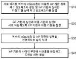
도 1을 참조하면, 본 발명의 실시예에 따른 InP 기판을 이용한 소자 제조 방법은 서로 이격된 복수의 InGaAs층이 매립된 InP 기판 상에 제 1 반도체소자를 형성하는 단계와 InP 기판과 상이한 이종 기판 상에 제 2 반도체소자를 형성하는 단계(S10); 상기 InP 기판의 상면과 상기 이종 기판의 상면이 서로 대향하도록 상기 InP 기판과 상기 이종 기판을 접합하는 단계(S20); 상기 복수의 InGaAs층 및 상기 InP 기판의 일부를 선택적으로 습식 식각하는 단계(S30); 및 상기 InP 기판의 나머지 부분에 비아홀을 형성하고 상기 비아홀에 도전성 패턴을 형성하는 단계(S40);를 포함할 수 있다.Referring to FIG. 1 , the device manufacturing method using an InP substrate according to an embodiment of the present invention includes the steps of forming a first semiconductor device on an InP substrate in which a plurality of InGaAs layers spaced apart from each other are buried, and a heterogeneous substrate different from the InP substrate. forming a second semiconductor device thereon (S10); bonding the InP substrate and the heterogeneous substrate so that an upper surface of the InP substrate and an upper surface of the heterogeneous substrate face each other (S20); selectively wet etching a portion of the plurality of InGaAs layers and the InP substrate (S30); and forming a via hole in the remaining portion of the InP substrate and forming a conductive pattern in the via hole (S40).
도 2 내지 도 6은 본 발명의 실시예에 따른 InP 기판을 이용한 소자 제조 방법을 순차적으로 도해하는 도면들이다.2 to 6 are views sequentially illustrating a device manufacturing method using an InP substrate according to an embodiment of the present invention.
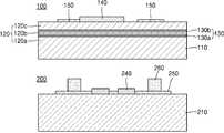
도 2를 참조하면, 서로 이격된 복수의 InGaAs층(130)이 매립된 InP 기판(110) 상에 제 1 반도체소자(140)를 형성하는 단계와 InP 기판과 상이한 이종 기판(210) 상에 제 2 반도체소자(240)를 형성하는 단계가 수행된다.Referring to FIG. 2 , a step of forming a
서로 이격된 복수의 InGaAs층(130)은 후속 공정에서 식각 정지층(etch-stop layer)으로 기능할 수 있다.The plurality of
상기 서로 이격된 복수의 InGaAs층(130)이 매립된 InP 기판(110)은, 제 1 InP층(120a) 상에 제 1 InGaAs층(130a)을 성장시키는 단계; 상기 제 1 InGaAs층(130a) 상에 제 2 InP층(120b)을 성장시키는 단계; 상기 제 2 InP층(120b) 상에 제 2 InGaAs층(130b)을 성장시키는 단계; 및 상기 제 2 InGaAs층(130b) 상에 제 3 InP층(120c)을 성장시키는 단계;를 포함하여 수행함으로써 구현될 수 있다.The
InGaAs 물질은 특정 In과 Ga간 조성비(In: 53%, Ga: 47%)에서 InP와 원자 격자상수(lattice constant)가 5.8687Å로 일치하여, 어떠한 격자 부정합(lattice mismatch)없이 InP 기판 상에 InGaAs 에피성장이 가능하다. 이에 InP 기판 상에 InGaAs를 성장시키고 이어서 InP층을 성장시키는, InP 내 얇은 InGaAs 층이 삽입된 형태의 InP 기판 기반 다층구조를 만들 수 있다.The InGaAs material has an InP and atomic lattice constant of 5.8687 Å at a specific In-Ga composition ratio (In: 53%, Ga: 47%), so that InGaAs on the InP substrate without any lattice mismatch Epi growth is possible. Accordingly, it is possible to make an InP substrate-based multi-layer structure in which InGaAs is grown on an InP substrate and then an InP layer is grown, in which a thin InGaAs layer is inserted in InP.
상기 서로 이격된 복수의 InGaAs층(130)이 2개의 InGaAs층으로 구성될 경우, 제 1 InP층(120a)은 최초의 InP 기판이며, 제 3 InP층(120c)은 InP 활성층(active layer)이며, 제 2 InP층(120b)은 서로 이격된 2개의 InGaAs층(130) 사이에 개재된 층으로 이해할 수 있다.When the plurality of
한편, 도 2에서는 서로 이격된 복수의 InGaAs층(130)을 2개의 층으로 도시하였으나, 본 발명이 이에 한정되는 것은 아니며, 예를 들어, 서로 이격된 3개 이상의 InGaAs층으로 확장될 수도 있다.Meanwhile, in FIG. 2 , a plurality of
상기 InP 기판과 상이한 이종 기판(210)은 InP과 상이한 임의의 물질로 이루어진 기판이며, 예를 들어, Si 기판, SiC 기판 또는 GaN 기판을 포함할 수 있다.The
상기 제 1 반도체 소자(140) 또는 상기 제 2 반도체 소자(240)는 포토리소그라피(photo-lithography), 금속 증착(metal deposition), 식각(etching) 등의 반도체 공정을 수행하여 형성할 수 있다.The
상기 제 1 반도체 소자(140) 또는 상기 제 2 반도체 소자(240)는 HEMT 소자(high electron mobility transistor), HBT 소자(heterojunction bipolar transistor), RTD 소자(resonant tunneling diode), FET 소자(Field effect transistor), TD 소자(tunneling diode), PD 소자(Photo diode) 또는 CMOS 소자(complementary metal oxide semiconductor)를 포함할 수 있다.The
예를 들어, 상기 제 1 반도체 소자(140)는 HBT 소자, HEMT 소자, RTD 소자 또는 FET 소자를 포함할 수 있고, 상기 제 2 반도체 소자(240)는 Si CMOS 소자, FET 소자, GaN HEMT 소자 또는 GaN HBT 소자 등을 포함할 수 있다.For example, the
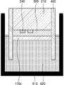
서로 이격된 복수의 InGaAs층(130)이 매립된 InP 기판(110) 상에 제 1 반도체소자(140) 뿐만 아니라 연결 금속배선(150)을 형성할 수 있으며, 이종 기판(210) 상에 제 2 반도체소자(240) 뿐만 아니라 연결 금속배선(250)을 형성할 수 있다. 또한, 이종 기판(210) 상에 범프(260)를 형성할 수 있다. 범프(260)는, 예를 들어, 전기 도금 기반의 공정으로 형성될 수 있다. 연결 금속배선(150, 250) 및 범프(260)는 회로 및 시스템 내의 입출력 단자 및 측정용 단자의 적어도 일부를 구성할 수 있다. 상기 범프는 이종 기판(210) 뿐만 아니라 InP 기판(110) 상에도 형성될 수 있다.The
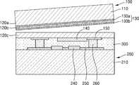
도 3을 참조하면, 상기 InP 기판(110)의 상면과 상기 이종 기판(210)의 상면이 서로 대향하도록 상기 InP 기판과 상기 이종 기판을 접합하는 단계가 수행된다.Referring to FIG. 3 , bonding the InP substrate and the heterogeneous substrate is performed so that the top surface of the
예를 들어, 제 1 반도체소자(140)가 상면에 형성되되 서로 이격된 복수의 InGaAs층(130)이 매립된 InP 기판(110)을 구비하는 제 1 구조체(100)와 제 2 반도체소자(240)가 상면에 형성된 이종 기판(210)을 구비하는 제 2 구조체(200) 중 어느 하나를 플립(flip)하여 상기 InP 기판(110)의 상면과 상기 이종 기판(210)의 상면이 서로 대향하도록 배치한 후, 제 1 구조체(100)와 제 2 구조체(200)를 접합한다.For example, the
상기 접합 과정에서 범프(260)는 제 1 구조체(100)에 형성된 연결 금속배선(150)과 제 2 구조체(200)에 형성된 연결 금속배선(250) 사이에 개재될 수 있다. 나아가, 제 1 구조체(100)와 제 2 구조체(200) 사이의 공간을 절연물질(300)로 충전(fill)할 수 있다.In the bonding process, the
도 4를 참조하면, 제 1 구조체(100)와 제 2 구조체(200)가 접합된 후, 제 1 반도체소자(140)가 상면에 형성되되 서로 이격된 복수의 InGaAs층(130)이 매립된 InP 기판(110)을 구비하는 제 1 구조체(100)에서 상기 복수의 InGaAs층(130) 및 상기 InP 기판의 일부(120a, 120b)를 선택적으로 제거하는 단계가 수행된다. 상기 복수의 InGaAs층(130) 및 상기 InP 기판의 일부(120a, 120b)를 선택적으로 제거하는 단계는 상기 복수의 InGaAs층(130) 및 상기 InP 기판의 일부(120a, 120b)를 선택적으로 습식 식각하는 단계를 포함할 수 있다.Referring to FIG. 4 , after the
예를 들어, 제 1 구조체(100)를 구성하는 서로 이격된 복수의 InGaAs층(130)이 매립된 InP 기판(110)의 두께는 600㎛ 이상이지만, 복수의 InGaAs층(130) 및 상기 InP 기판의 일부(120a, 120b)를 선택적으로 제거한 후 잔존하는 상기 InP 기판의 나머지(120c)는 두께가 수십㎛ 이하일 수 있다.For example, the thickness of the
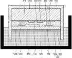
본 발명의 실시예에 따른 InP 기판을 이용한 소자 제조 방법에서 제 1 구조체(100)를 구성하는 InP층의 두께를 도 4와 같이 최종적으로 얇게 구현하는 이유는 기판 접합(wafer bonding)을 통해 형성된 회로 및 시스템 내의 입출력 단자 및 측정용 단자 등을 상부 표면으로 인출하는 구조(예를 들어, 비아홀 및 비아홀의 적어도 일부를 충전하는 도전성 패턴)를 용이하게 형성하기 위함이다.The reason for finally implementing the thin thickness of the InP layer constituting the
도 5 및 도 6을 참조하면, 복수의 InGaAs층(130) 및 상기 InP 기판의 일부(120a, 120b)를 선택적으로 제거한 후에, 상기 InP 기판의 나머지 부분(120c)에 비아홀(125)을 형성하고 상기 비아홀(125)에 도전성 패턴(170)을 형성하는 단계가 수행된다. 비아홀(125)에 형성된 도전성 패턴(170)은 회로 및 시스템 내의 입출력 단자 및 측정용 단자의 적어도 일부를 구성하는 연결 금속배선(150, 250) 및 범프(260)에 전기적으로 연결될 수 있다.5 and 6, after selectively removing the plurality of
제 1 구조체(100)를 구성하는 InP층의 두께를 도 4와 같이 최종적으로 얇게 구현할수록 비아홀(125)과 도전성 패턴(170)을 형성하는 공정의 난이도가 완화되고 연결저항값이 개선될 수 있다.As the thickness of the InP layer constituting the
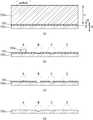
도 7 내지 도 12는 본 발명의 실시예에 따른 InP 기판을 이용한 소자 제조 방법 중 박형화 공정으로서 복수의 InGaAs층(130) 및 상기 InP 기판의 일부(120a, 120b)를 선택적으로 습식 식각하여 제거하는 공정을 순차적으로 도해하는 도면들이다.7 to 12 illustrate a method for manufacturing a device using an InP substrate according to an embodiment of the present invention, wherein a plurality of
도 7을 참조하면, 도 3에 개시된 제 1 구조체(100)와 제 2 구조체(200)의 접합 구조체의 가장자리에 보호물질층(400)을 형성하는 단계가 수행된다. 보호물질층(400)은, 예를 들어, 포토레지스트층을 포함할 수 있다. 보호물질층(400)은 접합 구조체의 적어도 측면에 형성되며, 나아가, 제 2 구조체(200)의 하면에도 형성될 수도 있으나, 제 1 구조체(100)의 하면은 노출되도록 형성되어야 한다.Referring to FIG. 7 , the step of forming the
도 7 및 도 8을 참조하면, 제 1 용기(510)에 수용된 제 1 식각용액(520)에 도 7에 개시된 접합 구조체를 뒤집어 침지시켜 제 1 구조체(100)를 구성하는 제 1 InP층(120a)을 식각하는 단계가 수행된다.7 and 8 , the
제 1 식각용액(520)은 InP 물질과 InGaAs 물질의 식각 선택비가 의미있는 수준으로 구현되도록 선택될 수 있다. 예를 들어, 제 1 식각용액(520)은 HCl 용액을 포함할 수 있으며, 제 1 식각용액(520)에서 InP 물질과 InGaAs 물질의 식각 선택비는 1000 : 1 내외의 범위일 수 있다. 이 경우, 제 1 식각용액(520)에서 제 1 InP층(120a)이 식각되는 동안 제 1 InGaAs층(130a)은 식각 정지층(etch-stop layer)으로 기능할 수 있다.The
도 8 및 도 9를 참조하면, 제 2 용기(610)에 수용된 제 2 식각용액(620)에 도 8에 개시된 접합 구조체를 침지시켜 제 1 구조체(100)를 구성하는 제 1 InGaAs층(130a)을 식각하는 단계가 수행된다.8 and 9, the
제 2 식각용액(620)은 InGaAs 물질과 InP 물질의 식각 선택비가 의미있는 수준으로 구현되도록 선택될 수 있다. 예를 들어, 제 2 식각용액(620)은 H3PO4, H2O2 및 DI의 혼합용액을 포함할 수 있으며, 제 2 식각용액(620)에서 InGaAs 물질과 InP 물질의 식각 선택비는 100 : 1 내외의 범위일 수 있다.The
도 9 및 도 10을 참조하면, 제 1 용기(510)에 수용된 제 1 식각용액(520)에 도 9에 개시된 접합 구조체를 침지시켜 제 1 구조체(100)를 구성하는 제 2 InP층(120b)을 식각하는 단계가 수행된다.9 and 10 , the
제 1 식각용액(520)은 InP 물질과 InGaAs 물질의 식각 선택비가 의미있는 수준으로 구현되도록 선택될 수 있다. 예를 들어, 제 1 식각용액(520)은 HCl 용액을 포함할 수 있으며, 제 1 식각용액(520)에서 InP 물질과 InGaAs 물질의 식각 선택비는 1000 : 1 내외의 범위일 수 있다. 이 경우, 제 1 식각용액(520)에서 제 2 InP층(120b)이 식각되는 동안 제 2 InGaAs층(130b)은 식각 정지층(etch-stop layer)으로 기능할 수 있다.The
도 10 및 도 11을 참조하면, 제 2 용기(610)에 수용된 제 2 식각용액(620)에 도 10에 개시된 접합 구조체를 침지시켜 제 1 구조체(100)를 구성하는 제 2 InGaAs층(130b)을 식각하는 단계가 수행된다.10 and 11 , the
제 2 식각용액(620)은 InGaAs 물질과 InP 물질의 식각 선택비가 의미있는 수준으로 구현되도록 선택될 수 있다. 예를 들어, 제 2 식각용액(620)은 H3PO4, H2O2 및 DI의 혼합용액을 포함할 수 있으며, 제 2 식각용액(620)에서 InGaAs 물질과 InP 물질의 식각 선택비는 100 : 1 내외의 범위일 수 있다.The
도 11 및 도 12를 참조하면, 접합 구조체의 가장자리에 형성된 보호물질층(400)을 제거하는 단계가 수행된다. 도 12에 개시된 구조체에 대하여 도 5 및 도 6에 개시된 공정을 수행할 수 있다.11 and 12 , a step of removing the
지금까지 설명한 본 발명의 실시예에 따른 InP 기판을 이용한 소자 제조 방법에서 주요한 특징 중의 하나는 InP 박형화(thinning) 공정이다. InP 기판과 InP 활성층(active layer) 사이에 우수한 습식식각 선택비를 갖는 InGaAs 물질을 삽입한 InP 기판 다층구조물을 기존의 InP 기판 대신 사용하였다. 이 InP 기판 다층구조물을 뒤집어서 하부의 타기판 기반 구조물과 기판 접합(wafer bonding)하고, InP 기판과 InGaAs 층을 습식식각 공정으로 제거 해내는 InP/InGaAs 습식식각 공정기술을 InP 박형화 공정에 적용하였다.One of the main characteristics of the device manufacturing method using the InP substrate according to the embodiment of the present invention described so far is an InP thinning process. An InP substrate multilayer structure in which an InGaAs material having an excellent wet etch selectivity is inserted between the InP substrate and the InP active layer was used instead of the conventional InP substrate. InP/InGaAs wet etching process technology, in which the InP substrate multi-layer structure is turned over to wafer-bond the lower substrate-based structure, and the InP substrate and InGaAs layer are removed through a wet etching process, was applied to the InP thinning process.
이와 비교될 수 있는 제 1 비교예로서, 화학 기계적 연마(CMP) 공정을 이용한 InP 박형화(thinning) 공정을 제안할 수 있다. 하지만, InP CMP 장비는 범용되지 않아 일반 연구자들이 용이하게 이용하지 못하는 문제점이 있다. 그리고, InP 물질은 고유의 취성 특성으로 공정 과정에서 부스러지거나 깨지기 쉬운데, CMP 공정은 물리적으로 InP 구조물에 힘을 가하여 갈아내는 방식을 적용하므로 신중한 공정 컨트롤이 필요하여 공정 난이도가 높다는 문제점이 있다. 즉, CMP 장비의 미세 컨트롤의 한계가 있어, CMP 공정후 남게 되는 InP 활성층의 두께를 수 ㎛ 이하로 얇게 하는 것에 한계가 있다.As a first comparative example that can be compared with this, an InP thinning process using a chemical mechanical polishing (CMP) process may be proposed. However, since InP CMP equipment is not universal, there is a problem that general researchers cannot easily use it. In addition, the InP material is prone to crumbling or breaking during the process due to its inherent brittle properties. The CMP process physically applies force to the InP structure and grinds it, so careful process control is required and the process difficulty is high. That is, there is a limit in the fine control of the CMP equipment, and there is a limit in making the thickness of the InP active layer remaining after the CMP process as thin as several μm or less.
한편, 제 2 비교예로서, InP 기판에 매립된 InGaAs층이 복수가 아니라 단일층인 경우를 제안할 수 있다.Meanwhile, as a second comparative example, a case in which the InGaAs layers embedded in the InP substrate are not plural but a single layer may be proposed.
도 13 내지 도 19는 본 발명의 비교예로서 하나의 InGaAs층이 매립된 InP 기판을 이용한 소자 제조 방법을 순차적으로 도해하는 도면들이다.13 to 19 are views sequentially illustrating a device manufacturing method using an InP substrate in which one InGaAs layer is embedded as a comparative example of the present invention.
도 13을 참조하면, InP 기판과 상이한 이종 기판(210) 상에 제 2 반도체소자(240)를 형성하는 단계가 수행된다. 상기 제 2 반도체 소자(240)는 Si CMOS 소자, FET 소자 또는 GaN HEMT 소자 등을 포함할 수 있다.Referring to FIG. 13 , a step of forming the
도 14를 참조하면, 하나의 InGaAs층(130)이 매립된 InP 기판(120)을 뒤집어 제 2 반도체소자(240)가 형성된 이종 기판(210)과 접합하는 단계가 수행된다. 하나의 InGaAs층(130)이 매립된 InP 기판(120)은 제 1 InP층(120a) 상에 InGaAs층(130)을 성장시키는 단계; 상기 InGaAs층(130) 상에 제 2 InP층(120c)을 성장시키는 단계;를 포함하여 수행함으로써 구현될 수 있다. 제 1 InP층(120a)은 최초의 InP 기판이며, 제 2 InP층(120c)은 InP 활성층(active layer)으로 이해할 수 있다.Referring to FIG. 14 , the
도 15를 참조하면, 도 14에 개시된 접합 구조체의 가장자리에 보호물질층(400)이 형성되는 단계가 수행된다.Referring to FIG. 15 , a step of forming the
도 15 및 도 16을 참조하면, 제 1 용기(510)에 수용된 제 1 식각용액(520)에 도 15에 개시된 접합 구조체를 뒤집어 침지시켜 제 1 InP층(120a)을 식각하는 단계가 수행된다.15 and 16 , the
제 1 식각용액(520)은 InP 물질과 InGaAs 물질의 식각 선택비가 의미있는 수준으로 구현되도록 선택될 수 있다. 예를 들어, 제 1 식각용액(520)은 HCl 용액을 포함할 수 있으며, 제 1 식각용액(520)에서 InP 물질과 InGaAs 물질의 식각 선택비는 1000 : 1 내외의 범위일 수 있다. 이 경우, 제 1 식각용액(520)에서 제 1 InP층(120a)이 식각되는 동안 InGaAs층(130)은 식각 정지층(etch-stop layer)으로 기능할 수 있다.The
도 16 및 도 17을 참조하면, 제 2 용기(610)에 수용된 제 2 식각용액(620)에 도 16에 개시된 접합 구조체를 침지시켜 InGaAs층(130)을 식각하는 단계가 수행된다.16 and 17 , the
제 2 식각용액(620)은 InGaAs 물질과 InP 물질의 식각 선택비가 의미있는 수준으로 구현되도록 선택될 수 있다. 예를 들어, 제 2 식각용액(620)은 H3PO4, H2O2 및 DI의 혼합용액을 포함할 수 있으며, 제 2 식각용액(620)에서 InGaAs 물질과 InP 물질의 식각 선택비는 100 : 1 내외의 범위일 수 있다.The
도 17 및 도 18을 참조하면, 접합 구조체의 가장자리에 형성된 보호물질층(400)을 제거하는 단계가 수행된다.17 and 18 , a step of removing the
도 19를 참조하면, InP 활성층(active layer)으로서 제 2 InP층(120c) 상에 제 1 반도체 소자(140)를 형성하는 단계가 수행된다. 예를 들어, 상기 제 1 반도체 소자(140)는 HBT 소자, HEMT 소자, RTD 소자 또는 FET 소자를 포함할 수 있다. 계속하여, 제 1 반도체 소자(140)와 제 2 반도체 소자(240)를 전기적으로 연결하는 연결 패턴(180)을 형성할 수 있다.Referring to FIG. 19 , a step of forming the
도 13 내지 도 19에 개시된 제 2 비교예는 제 2 반도체 소자(240)인 반도체 소자를 이미 형성한 타기판 기반 구조물과 아직 반도체소자를 형성하지 않은 InP 기판 기반 다층구조물을 기판 접합(wafer bonder) 장비를 활용하여 3차원 집적한 다이렉트 본딩 기술을 적용한 것이다. 다이렉트 본딩된 구조물에 대하여 InP/InGaAs 선택적 습식식각으로 InP 기판과 InGaAs 식각 정지층을 제거하고 상부 소자인 제 1 반도체 소자(140)를 순차적으로 형성하는 구성을 개시한다. 그러나, 다이렉트 본딩 공정 후 상부 소자인 제 1 반도체 소자(140)를 형성하는 과정에서 재성장(regrowth), 이온주입(implantation)과 같은 500℃ 이상의 고온 공정이 수행되면 하부 타기반 구조물 상의 반도체 소자(240)의 성능이 열화되는 문제점이 발생할 수 있다.The second comparative example disclosed in FIGS. 13 to 19 is a wafer bonder between another substrate-based structure in which a semiconductor element, which is the
나아가, 비교예2에 의하면 균일한 InP 활성층을 구현하는 것이 용이하지 않다는 문제점을 가지는 바, 이하에서 이를 상세하게 설명한다.Furthermore, according to Comparative Example 2, there is a problem that it is not easy to implement a uniform InP active layer, which will be described in detail below.
도 20은 본 발명의 비교예2에 따른 InP 기판을 이용한 소자 제조 방법을 순차적으로 도해하는 도면이다.20 is a diagram sequentially illustrating a device manufacturing method using an InP substrate according to Comparative Example 2 of the present invention.
도 20의 (a)를 참조하면, 하나의 InGaAs층(130)이 매립된 InP 기판은 제 1 InP층(120a) 상에 InGaAs층(130)을 성장시키는 단계; 상기 InGaAs층(130) 상에 제 2 InP층(120c)을 성장시키는 단계;를 포함하여 수행함으로써 구현될 수 있다. 제 1 InP층(120a)은 최초의 InP 기판이며, InGaAs층(130)은 식각 정지층이며, 제 2 InP층(120c)은 InP 활성층(active layer)으로 이해할 수 있다. 예를 들어, 제 1 InP층(120a)의 두께(t1)는 650㎛이며, InGaAs층(130)의 두께(t2)는 0.5㎛이며, 제 2 InP층(120c)의 두께(t3)는 1 ㎛ 이상일 수 있다.Referring to FIG. 20A , the InP substrate in which one
도 20의 (b)를 참조하면, 하나의 InGaAs층(130)이 매립된 InP 기판에 대하여 InP 습식식각을 수행하여 제 1 InP층(120a)을 제거한다. InP 습식식각을 위한 제 1 식각용액은 HCl 용액을 포함할 수 있다. 제 1 식각용액(520)에서 InP 물질과 InGaAs 물질의 식각 선택비는 1000 : 1 내외의 범위일 수 있다. 이 경우, 제 1 InP층(120a) 상에 존재하는 파티클(particle)에 의하여 InP 기판의 잔여물(120p)이 형성될 수 있으며(A), HCl 용액의 불일정한 InP 식각 특성으로 불균일한 InGaAs 표면 프로파일(surface profile)이 형성될 수 있다(B, C, D).Referring to (b) of FIG. 20 , the
도 20의 (c)를 참조하면, InP 기판의 잔여물(120p)을 제거하기 위하여 추가적으로 InP 습식식각을 수행할 수 있다. 이 과정에서, InGaAs층(130)은 파티클로 인한 불균일 InGaAs 프로파일이 형성되며(A), InGaAs 식각 정지층이 뚫리는 현상이 발생하며(B), 불균일한 InGaAs 표면 프로파일(surface profile)이 심화될 수 있다(C, D). HCl 용액의 InP 식각 속도는 10㎛/min 내외로서, 불균일 InGaAs 프로파일 (A)이 모두 제거되는 순간을 실험자가 눈으로 확인한후 그 식각을 멈추면 비록 순간적일지라도 수백 nm의 InP 활성층 손실이 발생할 수 있다. 이러한 활성층 손실은 그 활성층의 두께가 수백 nm 이하일 경우, 대면적 웨이퍼간 삼차원 집적 공정의 수율 저하를 초래하는 치명적 결과를 가져온다. Referring to FIG. 20C , InP wet etching may be additionally performed to remove the
도 20의 (d)를 참조하면, InGaAs 습식식각을 수행하여 InGaAs층(130)을 제거한다. InGaAs 습식식각을 위한 제 2 식각용액은 H3PO4, H2O2 및 DI의 혼합용액을 포함할 수 있다. 제 2 식각용액(620)에서 InGaAs 물질과 InP 물질의 식각 선택비는 100 : 1 내외의 범위일 수 있다. 이 과정에서 InP 활성층(active layer)인 제 2 InP층(120c)에 불균일한 InP 표면 프로파일이 형성될 수 있다(A, B, C, D).Referring to FIG. 20D , the
도 20에 개시된 비교예에 의하면, InP 기판 습식식각이 불균일하게 이루어짐을 확인할 수 있다. InP 기판 습식식각이 불균일하게 이루어지는 경우, 삽입한 InGaAs 층 내 특정 부분이 먼저 제거가 되고, 최종적으로 구현된 InP 활성층의 표면이 울퉁불퉁하게 형성되거나, 특정 지역이 완전히 제거되어 후속의 상호연결(Interconnection) 공정 후 회로 및 시스템 내 특정 부분이 전기적으로 단락(short)되어 소자 동작이 불가능해지는 문제점이 나타날 수 있다.According to the comparative example disclosed in FIG. 20 , it can be seen that the wet etching of the InP substrate is non-uniform. In the case of non-uniform wet etching of the InP substrate, a specific portion in the inserted InGaAs layer is removed first, and the surface of the finally implemented InP active layer is formed to be uneven, or a specific area is completely removed for subsequent interconnection. After the process, a specific part in the circuit and the system is electrically shorted, which may cause a problem in that device operation becomes impossible.
또한, 도 20에 개시된 비교예에 의하면, InP 습식식각 용액(예를 들어, HCl) 의 InP와 InGaAs 간 식각선택비는 1000 대 1 내외 수준이다. InP 기판의 두께는 일반적으로 600 ~ 700㎛ 수준으로, InGaAs 식각 정지층을 1㎛ 이상으로 매우 두껍게 성장시킨다면 식각 불균일에 의한 InP 활성층 분균일 현상의 해결이 가능할 수 있다. 그러나, InGaAs 층이 두꺼우면 후속 에피성장의 성장 공정의 난이도가 증가하고 성장 비용이 증가하는 문제점이 나타난다.In addition, according to the comparative example shown in FIG. 20, the etch selectivity between InP and InGaAs of the InP wet etching solution (eg, HCl) is about 1000 to 1. The thickness of the InP substrate is generally 600 to 700 μm, and if the InGaAs etch stop layer is grown to a very thick thickness of 1 μm or more, it may be possible to solve the unevenness of the InP active layer caused by the etch non-uniformity. However, when the InGaAs layer is thick, the difficulty of the subsequent epi-growth growth process increases and the growth cost increases.
도 21은 본 발명의 실시예에 따른 InP 기판을 이용한 소자 제조 방법을 순차적으로 도해하는 도면이다.21 is a diagram sequentially illustrating a method of manufacturing a device using an InP substrate according to an embodiment of the present invention.
도 21의 (a)를 참조하면, 서로 이격된 복수의 InGaAs층(130a, 130b)이 매립된 InP 기판은, 제 1 InP층(120a) 상에 제 1 InGaAs층(130a)을 성장시키는 단계; 상기 제 1 InGaAs층(130a) 상에 제 2 InP층(120b)을 성장시키는 단계; 상기 제 2 InP층(120b) 상에 제 2 InGaAs층(130b)을 성장시키는 단계; 및 상기 제 2 InGaAs층(130b) 상에 제 3 InP층(120c)을 성장시키는 단계;를 포함하여 수행함으로써 구현될 수 있다. 제 1 InP층(120a)은 최초의 InP 기판이며, 제 3 InP층(120c)은 InP 활성층(active layer)이며, 제 2 InP층(120b)은 서로 이격된 2개의 InGaAs층(130) 사이에 개재된 층으로 이해할 수 있다. 예를 들어, 제 1 InP층(120a)의 두께(t1)는 650㎛이며, 제 1 InGaAs층(130a)의 두께(t2)는 0.5㎛이며, 제 2 InP층(120b)의 두께(t3)는 0.5㎛이며, 제 2 InGaAs층(130b)의 두께(t4)는 0.02㎛이며, 제 3 InP층(120c)의 두께(t5)는 0.01 이상㎛일 수 있다.Referring to FIG. 21A , the InP substrate in which a plurality of
도 20에 개시된 비교예 구조의 두께 t2, t3의 합(최소값)은 1.5㎛인 반면, 도 21에 개시된 실시예 구조의 두께 t2, t3, t4, t5의 합 (최소값)은 1.03㎛으로서, 실시예 구조의 총 두께가 더 얇아 에피 성장의 난이도 및 비용 측면에서도 더 유리하다.The sum (minimum value) of the thicknesses t2, t3 of the comparative example structure disclosed in FIG. 20 is 1.5 μm, while the sum (minimum value) of the thicknesses t2, t3, t4, and t5 of the embodiment structure disclosed in FIG. 21 is 1.03 μm. Yes, the total thickness of the structure is thinner, which is more advantageous in terms of difficulty and cost of epi-growth.
도 21의 (b)를 참조하면, 서로 이격된 복수의 InGaAs층(130a, 130b)이 매립된 InP 기판에 대하여 InP 습식식각을 수행하여 제 1 InP층(120a)을 제거한다. InP 습식식각을 위한 제 1 식각용액은 HCl 용액을 포함할 수 있다. 제 1 식각용액(520)에서 InP 물질과 InGaAs 물질의 식각 선택비는 1000 : 1 내외의 범위일 수 있다. 이 경우, 제 1 InP층(120a) 상에 존재하는 파티클(particle)에 의하여 InP 기판의 잔여물(120p)이 형성될 수 있으며(A), HCl 용액의 불일정한 InP 식각 특성으로 불균일한 InGaAs 표면 프로파일(surface profile)이 형성될 수 있다(B, C, D).Referring to FIG. 21B , the
도 21의 (c)를 참조하면, InP 기판의 잔여물(120p)을 제거하기 위하여 추가적으로 InP 습식식각을 수행할 수 있다. 이 과정에서, 제 1 InGaAs층(130a)은 파티클로 인한 불균일 InGaAs 프로파일이 형성되며(A), 식각 정지층인 제 1 InGaAs층(130a)이 뚫리는 현상이 발생하며(B), 불균일한 InGaAs 표면 프로파일(surface profile)이 심화될 수도 있다(C, D).Referring to FIG. 21C , InP wet etching may be additionally performed to remove the
도 21의 (d)를 참조하면, InGaAs 습식식각을 수행하여 제 1 InGaAs층(130a)을 제거한다. InGaAs 습식식각을 위한 제 2 식각용액은 H3PO4, H2O2 및 DI의 혼합용액을 포함할 수 있다. 제 2 식각용액(620)에서 InGaAs 물질과 InP 물질의 식각 선택비는 100 : 1 내외의 범위일 수 있다. 이 과정에서 제 2 InP층(120b)에 불균일한 InP 표면 프로파일이 형성될 수 있다(A, B, C, D). 그러나, 제 2 InP층(120b)에 형성되는 불균일한 InP 표면 프로파일은 제 2 InGaAs층(130b)의 존재로 인하여 제한된다.Referring to FIG. 21D , the
도 21의 (e)를 참조하면, InP 습식식각을 수행하여 제 2 InP층(120b)을 제거한다. InP 습식식각을 위한 제 1 식각용액은 HCl 용액을 포함할 수 있다. 제 1 식각용액(520)에서 InP 물질과 InGaAs 물질의 식각 선택비는 1000 : 1 내외의 범위일 수 있다. 이 경우, 제 2 InP층(120b)에 형성되는 불균일한 InP 표면 프로파일은 제거되며, 식각 정지층인 제 2 InGaAs층(130b)의 존재로 인하여 제 2 InP층(120b)에 형성되는 불균일한 InP 표면 프로파일은 제 3 InP층(120c)으로 진행되지 않는다. 계속하여, InGaAs 습식식각을 수행하여 제 2 InGaAs층(130b)을 제거한다. InGaAs 습식식각을 위한 제 2 식각용액은 H3PO4, H2O2 및 DI의 혼합용액을 포함할 수 있다. 제 2 식각용액(620)에서 InGaAs 물질과 InP 물질의 식각 선택비는 100 : 1 내외의 범위일 수 있다.Referring to FIG. 21E , the
이에 의하면, 최종적으로 구현된 InP 활성층으로서 제 3 InP층(120c)은 균일한 프로파일을 가지며, 더욱 얇은 두께를 가질 수 있다. InP 활성층으로서 제 3 InP층(120c)의 두께가 균일하면서 얇을 경우, 기판 접합(wafer bonding)을 통해 형성된 회로 및 시스템 내의 입출력 단자 및 측정용 단자 등을 상부 표면으로 인출하는 구조(예를 들어, 비아홀 및 비아홀의 적어도 일부를 충전하는 도전성 패턴)를 용이하게 형성할 수 있으며, 연결저항이 현저하게 감소되는 유리한 효과를 기대할 수 있다.Accordingly, the
도 20의 비교예2와 도 21의 실시예를 검토하면, 최종적으로 구현되는 InP 활성층의 두께를 균일하고 더욱 얇게 확보함에 있어서, 하나의 InGaAs층이 매립된 InP 기판을 이종 기판에 접합하는 것보다 서로 이격된 복수의 InGaAs층이 매립된 InP 기판을 이종 기판에 접하는 것이 유리함을 확인할 수 있다. 서로 다른 식각용액으로 각각 InP 물질과 InGaAs 물질을 식각 제거하는 과정에서, 복수의 InGaAs층이 매립된 InP 기판에서는 불일정한 식각 특성이 확대 전파되는 것이 완화됨을 확인하였다.Examining the comparative example 2 of FIG. 20 and the example of FIG. 21 , in securing a uniform and thinner thickness of the finally implemented InP active layer, it is better than bonding an InP substrate in which one InGaAs layer is embedded to a heterogeneous substrate. It can be seen that it is advantageous to contact an InP substrate in which a plurality of InGaAs layers spaced apart from each other are buried in contact with a heterogeneous substrate. In the process of etching and removing the InP material and the InGaAs material with different etching solutions, it was confirmed that the spread of inconsistent etching characteristics was alleviated in the InP substrate in which the plurality of InGaAs layers were buried.
본 발명은 도면에 도시된 실시예를 참고로 설명되었으나 이는 예시적인 것에 불과하며, 당해 기술분야에서 통상의 지식을 가진 자라면 이로부터 다양한 변형 및 균등한 다른 실시예가 가능하다는 점을 이해할 것이다. 따라서 본 발명의 진정한 기술적 보호 범위는 첨부된 특허청구범위의 기술적 사상에 의하여 정해져야 할 것이다.Although the present invention has been described with reference to the embodiment shown in the drawings, which is merely exemplary, those skilled in the art will understand that various modifications and equivalent other embodiments are possible therefrom. Therefore, the true technical protection scope of the present invention should be determined by the technical spirit of the appended claims.
Claims (7)
Translated fromKoreanInP 기판과 상이한 이종 기판 상에 제 2 반도체소자를 형성하는 단계;
상기 InP 기판의 상면과 상기 이종 기판의 상면이 서로 대향하도록 상기 InP 기판과 상기 이종 기판을 접합하는 단계; 및
상기 복수의 InGaAs층 및 상기 InP 기판의 일부를 선택적으로 습식 식각하는 단계;를 포함하되,
상기 서로 이격된 복수의 InGaAs층이 매립된 InP 기판은, 제 1 InP층, 상기 제 1 InP층 상의 제 1 InGaAs층, 상기 제 1 InGaAs층 상의 제 2 InP층, 상기 제 2 InP층 상의 제 2 InGaAs층, 상기 제 2 InGaAs층 상의 제 3 InP층을 포함하는,
InP 기판을 이용한 소자 제조 방법.forming a first semiconductor device on an InP substrate in which a plurality of InGaAs layers spaced apart from each other are buried;
forming a second semiconductor device on a heterogeneous substrate different from the InP substrate;
bonding the InP substrate and the heterogeneous substrate such that an upper surface of the InP substrate and an upper surface of the heterogeneous substrate face each other; and
Selectively wet-etching a portion of the plurality of InGaAs layers and the InP substrate;
The InP substrate in which a plurality of InGaAs layers spaced apart from each other are buried, includes a first InP layer, a first InGaAs layer on the first InP layer, a second InP layer on the first InGaAs layer, and a second on the second InP layer an InGaAs layer, comprising a third InP layer on the second InGaAs layer;
A device manufacturing method using an InP substrate.
상기 서로 이격된 복수의 InGaAs층이 매립된 InP 기판은, 제 1 InP층 상에 제 1 InGaAs층을 성장시키는 단계; 상기 제 1 InGaAs층 상에 제 2 InP층을 성장시키는 단계; 상기 제 2 InP층 상에 제 2 InGaAs층을 성장시키는 단계; 및 상기 제 2 InGaAs층 상에 제 3 InP층을 성장시키는 단계;를 포함하여 수행함으로써 구현된,
InP 기판을 이용한 소자 제조 방법.The method of claim 1,
The InP substrate in which a plurality of InGaAs layers spaced apart from each other are buried, the method comprising: growing a first InGaAs layer on the first InP layer; growing a second InP layer on the first InGaAs layer; growing a second InGaAs layer on the second InP layer; and growing a third InP layer on the second InGaAs layer.
A device manufacturing method using an InP substrate.
상기 복수의 InGaAs층 및 상기 InP 기판의 일부를 선택적으로 습식 식각하는 단계;는 제 1 식각용액을 이용하여 제 1 InP층을 식각하는 단계; 제 2 식각용액을 이용하여 제 1 InGaAs층을 식각하는 단계; 제 1 식각용액을 이용하여 제 2 InP층을 식각하는 단계; 및 제 2 식각용액을 이용하여 제 2 InGaAs층을 식각하는 단계;를 순차적으로 포함하는,
InP 기판을 이용한 소자 제조 방법.3. The method of claim 2,
The selective wet etching of the plurality of InGaAs layers and a portion of the InP substrate may include: etching the first InP layer using a first etching solution; etching the first InGaAs layer using a second etching solution; etching the second InP layer using the first etching solution; and etching the second InGaAs layer using a second etching solution;
A device manufacturing method using an InP substrate.
상기 제 1 식각용액은 HCl 용액을 포함하고, 상기 제 2 식각용액은 H3PO4, H2O2 및 DI의 혼합용액을 포함하는,
InP 기판을 이용한 소자 제조 방법.4. The method of claim 3,
The first etching solution includes a HCl solution, and the second etching solution includes a mixed solutionof H 3 PO4 , H2 O2 and DI,
A device manufacturing method using an InP substrate.
상기 제 1 반도체 소자 또는 상기 제 2 반도체 소자는 HEMT 소자(high electron mobility transistor), HBT 소자(heterojunction bipolar transistor), RTD 소자(resonant tunneling diode), FET 소자(Field effect transistor), TD 소자(tunneling diode), PD 소자(Photo diode) 또는 CMOS 소자(complementary metal oxide semiconductor)를 포함하는,
InP 기판을 이용한 소자 제조 방법.The method of claim 1,
The first semiconductor device or the second semiconductor device may include a high electron mobility transistor (HEM) device, a heterojunction bipolar transistor (HBT device), a resonant tunneling diode (RTD), a field effect transistor (FET), and a tunneling diode (TD) device. ), including a PD device (Photo diode) or CMOS device (complementary metal oxide semiconductor),
A device manufacturing method using an InP substrate.
상기 InP 기판과 상이한 이종 기판은 Si 기판, SiC 기판 또는 GaN 기판을 포함하는,
InP 기판을 이용한 소자 제조 방법.The method of claim 1,
The heterogeneous substrate different from the InP substrate comprises a Si substrate, a SiC substrate or a GaN substrate,
A device manufacturing method using an InP substrate.
InP 기판과 상이한 이종 기판 상에 제 2 반도체소자를 형성하는 단계;
상기 InP 기판의 상면과 상기 이종 기판의 상면이 서로 대향하도록 상기 InP 기판과 상기 이종 기판을 접합하는 단계; 및
상기 복수의 InGaAs층 및 상기 InP 기판의 일부를 선택적으로 습식 식각하는 단계;를 포함하며,
상기 복수의 InGaAs층 및 상기 InP 기판의 일부를 선택적으로 습식 식각하는 단계; 후에 상기 InP 기판의 나머지 부분에 비아홀을 형성하고 상기 비아홀에 도전성 패턴을 형성하는 단계;를 더 포함하는,
InP 기판을 이용한 소자 제조 방법.forming a first semiconductor device on an InP substrate in which a plurality of InGaAs layers spaced apart from each other are buried;
forming a second semiconductor device on a heterogeneous substrate different from the InP substrate;
bonding the InP substrate and the heterogeneous substrate such that an upper surface of the InP substrate and an upper surface of the heterogeneous substrate face each other; and
and selectively wet-etching a portion of the plurality of InGaAs layers and the InP substrate;
selectively wet etching the plurality of InGaAs layers and portions of the InP substrate; After forming a via hole in the remaining portion of the InP substrate and forming a conductive pattern in the via hole; further comprising
A device manufacturing method using an InP substrate.
Priority Applications (1)
| Application Number | Priority Date | Filing Date | Title |
|---|---|---|---|
| KR1020210078487AKR102322540B1 (en) | 2021-06-17 | 2021-06-17 | Methods of fabricating device using InP substrate |
Applications Claiming Priority (1)
| Application Number | Priority Date | Filing Date | Title |
|---|---|---|---|
| KR1020210078487AKR102322540B1 (en) | 2021-06-17 | 2021-06-17 | Methods of fabricating device using InP substrate |
Publications (1)
| Publication Number | Publication Date |
|---|---|
| KR102322540B1true KR102322540B1 (en) | 2021-11-09 |
Family
ID=78610419
Family Applications (1)
| Application Number | Title | Priority Date | Filing Date |
|---|---|---|---|
| KR1020210078487AActiveKR102322540B1 (en) | 2021-06-17 | 2021-06-17 | Methods of fabricating device using InP substrate |
Country Status (1)
| Country | Link |
|---|---|
| KR (1) | KR102322540B1 (en) |
Citations (7)
| Publication number | Priority date | Publication date | Assignee | Title |
|---|---|---|---|---|
| KR20070112695A (en) | 2006-05-22 | 2007-11-27 | 미쓰비시덴키 가부시키가이샤 | Field effect transistor |
| JP2009253022A (en)* | 2008-04-07 | 2009-10-29 | Sony Corp | Method of manufacturing semiconductor device |
| WO2014017063A1 (en)* | 2012-07-24 | 2014-01-30 | 住友化学株式会社 | Semiconductor substrate, method for manufacturing semiconductor substrate, and method for manufacturing composite substrate |
| KR20150032845A (en)* | 2012-06-15 | 2015-03-30 | 스미또모 가가꾸 가부시키가이샤 | Method of producing composite wafer and composite wafer |
| KR20150038335A (en)* | 2012-07-30 | 2015-04-08 | 스미또모 가가꾸 가부시키가이샤 | Method for manufacturing composite substrate and method for manufacturing semiconductor crystal layer formation substrate |
| KR20160136103A (en)* | 2015-05-19 | 2016-11-29 | 한국과학기술연구원 | Method for manufacturing semiconductor device using high speed epitaxial lift-off and template for iii-v direct growth and semiconductor device manufactured using the same |
| US20170200700A1 (en)* | 2014-08-11 | 2017-07-13 | Massachusetts Institute Of Technology | Interconnect Structures for Assembly of Multi-Layer Semiconductor Devices |
- 2021
- 2021-06-17KRKR1020210078487Apatent/KR102322540B1/enactiveActive
Patent Citations (8)
| Publication number | Priority date | Publication date | Assignee | Title |
|---|---|---|---|---|
| KR20070112695A (en) | 2006-05-22 | 2007-11-27 | 미쓰비시덴키 가부시키가이샤 | Field effect transistor |
| JP2009253022A (en)* | 2008-04-07 | 2009-10-29 | Sony Corp | Method of manufacturing semiconductor device |
| KR20150032845A (en)* | 2012-06-15 | 2015-03-30 | 스미또모 가가꾸 가부시키가이샤 | Method of producing composite wafer and composite wafer |
| WO2014017063A1 (en)* | 2012-07-24 | 2014-01-30 | 住友化学株式会社 | Semiconductor substrate, method for manufacturing semiconductor substrate, and method for manufacturing composite substrate |
| KR20150038217A (en)* | 2012-07-24 | 2015-04-08 | 스미또모 가가꾸 가부시키가이샤 | Semiconductor substrate, method for manufacturing semiconductor substrate, and method for manufacturing composite substrate |
| KR20150038335A (en)* | 2012-07-30 | 2015-04-08 | 스미또모 가가꾸 가부시키가이샤 | Method for manufacturing composite substrate and method for manufacturing semiconductor crystal layer formation substrate |
| US20170200700A1 (en)* | 2014-08-11 | 2017-07-13 | Massachusetts Institute Of Technology | Interconnect Structures for Assembly of Multi-Layer Semiconductor Devices |
| KR20160136103A (en)* | 2015-05-19 | 2016-11-29 | 한국과학기술연구원 | Method for manufacturing semiconductor device using high speed epitaxial lift-off and template for iii-v direct growth and semiconductor device manufactured using the same |
Similar Documents
| Publication | Publication Date | Title |
|---|---|---|
| US9614046B2 (en) | Semiconductor devices with a thermally conductive layer | |
| CN106169470B (en) | Device having conductive features formed over a cavity and corresponding method | |
| TWI681505B (en) | Semiconductor device and method for manufacturing the same | |
| JP6345251B2 (en) | Method and structure for forming a microstrip transmission line on a thin silicon-on-insulator (SOI) wafer | |
| US6790694B2 (en) | High frequency semiconductor module, high frequency semiconductor device and manufacturing method for the same | |
| US12142643B2 (en) | Material structure for low thermal resistance silicon-based gallium nitride microwave and millimeter-wave devices and manufacturing method thereof | |
| US12266523B2 (en) | Parasitic capacitance reduction in GaN-on-silicon devices | |
| US9490214B2 (en) | Semiconductor device and method of fabricating the same | |
| US9691761B1 (en) | Monolithic integration of GaN and InP components | |
| US9761445B2 (en) | Methods and structures for forming microstrip transmission lines on thin silicon carbide on insulator (SICOI) wafers | |
| JP2001308108A (en) | Field effect transistor and method of manufacturing the same | |
| KR102322540B1 (en) | Methods of fabricating device using InP substrate | |
| JP3078420B2 (en) | Semiconductor device | |
| CN220341210U (en) | semiconductor structure | |
| CN114883192B (en) | Monolithic heterogeneous integrated structure of silicon and III-V devices on insulating substrate and preparation method thereof | |
| CN114072925A (en) | Semiconductor structure and preparation method thereof | |
| JP2000349088A (en) | Semiconductor device and manufacturing method thereof | |
| CN114450804B (en) | Nitride-based semiconductor circuit and method for manufacturing the same | |
| CN114503261B (en) | Nitride-based semiconductor circuit and method for manufacturing the same | |
| CN114388496B (en) | Device integration scheme using bulk semiconductor substrate | |
| KR100811492B1 (en) | BaN-based electronic device manufacturing method | |
| US20210217921A1 (en) | Semiconductor Structure Having Group III-V Device on Group IV Substrate and Contacts with Precursor Stacks | |
| CN116072531A (en) | Method for manufacturing electrode on side face of semiconductor functional area | |
| CN114388496A (en) | Device integration scheme utilizing bulk semiconductor substrates with <111> crystal orientation | |
| CN119997602A (en) | An integrated structure based on multi-material composite substrate construction and its manufacturing method |
Legal Events
| Date | Code | Title | Description |
|---|---|---|---|
| PA0109 | Patent application | Patent event code:PA01091R01D Comment text:Patent Application Patent event date:20210617 | |
| PA0201 | Request for examination | ||
| PA0302 | Request for accelerated examination | Patent event date:20210617 Patent event code:PA03022R01D Comment text:Request for Accelerated Examination | |
| PE0902 | Notice of grounds for rejection | Comment text:Notification of reason for refusal Patent event date:20210706 Patent event code:PE09021S01D | |
| E701 | Decision to grant or registration of patent right | ||
| PE0701 | Decision of registration | Patent event code:PE07011S01D Comment text:Decision to Grant Registration Patent event date:20211028 | |
| GRNT | Written decision to grant | ||
| PR0701 | Registration of establishment | Comment text:Registration of Establishment Patent event date:20211101 Patent event code:PR07011E01D | |
| PR1002 | Payment of registration fee | Payment date:20211102 End annual number:3 Start annual number:1 | |
| PG1601 | Publication of registration | ||
| PR1001 | Payment of annual fee | Payment date:20241024 Start annual number:4 End annual number:4 |