KR102312260B1 - Flexible touch panel and flexible display device - Google Patents
Flexible touch panel and flexible display deviceDownload PDFInfo
- Publication number
- KR102312260B1 KR102312260B1KR1020150003504AKR20150003504AKR102312260B1KR 102312260 B1KR102312260 B1KR 102312260B1KR 1020150003504 AKR1020150003504 AKR 1020150003504AKR 20150003504 AKR20150003504 AKR 20150003504AKR 102312260 B1KR102312260 B1KR 102312260B1
- Authority
- KR
- South Korea
- Prior art keywords
- flexible
- bridge
- touch
- touch panel
- flexible substrate
- Prior art date
- Legal status (The legal status is an assumption and is not a legal conclusion. Google has not performed a legal analysis and makes no representation as to the accuracy of the status listed.)
- Active
Links
Images


Classifications
- G—PHYSICS
- G06—COMPUTING OR CALCULATING; COUNTING
- G06F—ELECTRIC DIGITAL DATA PROCESSING
- G06F3/00—Input arrangements for transferring data to be processed into a form capable of being handled by the computer; Output arrangements for transferring data from processing unit to output unit, e.g. interface arrangements
- G06F3/01—Input arrangements or combined input and output arrangements for interaction between user and computer
- G06F3/03—Arrangements for converting the position or the displacement of a member into a coded form
- G06F3/041—Digitisers, e.g. for touch screens or touch pads, characterised by the transducing means
- G06F3/044—Digitisers, e.g. for touch screens or touch pads, characterised by the transducing means by capacitive means
- G06F3/0443—Digitisers, e.g. for touch screens or touch pads, characterised by the transducing means by capacitive means using a single layer of sensing electrodes
- G—PHYSICS
- G06—COMPUTING OR CALCULATING; COUNTING
- G06F—ELECTRIC DIGITAL DATA PROCESSING
- G06F3/00—Input arrangements for transferring data to be processed into a form capable of being handled by the computer; Output arrangements for transferring data from processing unit to output unit, e.g. interface arrangements
- G06F3/01—Input arrangements or combined input and output arrangements for interaction between user and computer
- G06F3/03—Arrangements for converting the position or the displacement of a member into a coded form
- G06F3/041—Digitisers, e.g. for touch screens or touch pads, characterised by the transducing means
- B—PERFORMING OPERATIONS; TRANSPORTING
- B65—CONVEYING; PACKING; STORING; HANDLING THIN OR FILAMENTARY MATERIAL
- B65H—HANDLING THIN OR FILAMENTARY MATERIAL, e.g. SHEETS, WEBS, CABLES
- B65H5/00—Feeding articles separated from piles; Feeding articles to machines
- B65H5/02—Feeding articles separated from piles; Feeding articles to machines by belts or chains, e.g. between belts or chains
- B65H5/021—Feeding articles separated from piles; Feeding articles to machines by belts or chains, e.g. between belts or chains by belts
- B65H5/025—Feeding articles separated from piles; Feeding articles to machines by belts or chains, e.g. between belts or chains by belts between belts and rotary means, e.g. rollers, drums, cylinders or balls, forming a transport nip
- G—PHYSICS
- G02—OPTICS
- G02F—OPTICAL DEVICES OR ARRANGEMENTS FOR THE CONTROL OF LIGHT BY MODIFICATION OF THE OPTICAL PROPERTIES OF THE MEDIA OF THE ELEMENTS INVOLVED THEREIN; NON-LINEAR OPTICS; FREQUENCY-CHANGING OF LIGHT; OPTICAL LOGIC ELEMENTS; OPTICAL ANALOGUE/DIGITAL CONVERTERS
- G02F1/00—Devices or arrangements for the control of the intensity, colour, phase, polarisation or direction of light arriving from an independent light source, e.g. switching, gating or modulating; Non-linear optics
- G02F1/01—Devices or arrangements for the control of the intensity, colour, phase, polarisation or direction of light arriving from an independent light source, e.g. switching, gating or modulating; Non-linear optics for the control of the intensity, phase, polarisation or colour
- G02F1/13—Devices or arrangements for the control of the intensity, colour, phase, polarisation or direction of light arriving from an independent light source, e.g. switching, gating or modulating; Non-linear optics for the control of the intensity, phase, polarisation or colour based on liquid crystals, e.g. single liquid crystal display cells
- G02F1/133—Constructional arrangements; Operation of liquid crystal cells; Circuit arrangements
- G02F1/1333—Constructional arrangements; Manufacturing methods
- G02F1/13338—Input devices, e.g. touch panels
- G—PHYSICS
- G03—PHOTOGRAPHY; CINEMATOGRAPHY; ANALOGOUS TECHNIQUES USING WAVES OTHER THAN OPTICAL WAVES; ELECTROGRAPHY; HOLOGRAPHY
- G03G—ELECTROGRAPHY; ELECTROPHOTOGRAPHY; MAGNETOGRAPHY
- G03G15/00—Apparatus for electrographic processes using a charge pattern
- G03G15/65—Apparatus which relate to the handling of copy material
- G03G15/6555—Handling of sheet copy material taking place in a specific part of the copy material feeding path
- G—PHYSICS
- G06—COMPUTING OR CALCULATING; COUNTING
- G06F—ELECTRIC DIGITAL DATA PROCESSING
- G06F1/00—Details not covered by groups G06F3/00 - G06F13/00 and G06F21/00
- G06F1/16—Constructional details or arrangements
- G06F1/1613—Constructional details or arrangements for portable computers
- G06F1/1633—Constructional details or arrangements of portable computers not specific to the type of enclosures covered by groups G06F1/1615 - G06F1/1626
- G06F1/1637—Details related to the display arrangement, including those related to the mounting of the display in the housing
- G06F1/1652—Details related to the display arrangement, including those related to the mounting of the display in the housing the display being flexible, e.g. mimicking a sheet of paper, or rollable
- G—PHYSICS
- G06—COMPUTING OR CALCULATING; COUNTING
- G06F—ELECTRIC DIGITAL DATA PROCESSING
- G06F3/00—Input arrangements for transferring data to be processed into a form capable of being handled by the computer; Output arrangements for transferring data from processing unit to output unit, e.g. interface arrangements
- G06F3/01—Input arrangements or combined input and output arrangements for interaction between user and computer
- G06F3/03—Arrangements for converting the position or the displacement of a member into a coded form
- G06F3/041—Digitisers, e.g. for touch screens or touch pads, characterised by the transducing means
- G06F3/0412—Digitisers structurally integrated in a display
- G—PHYSICS
- G06—COMPUTING OR CALCULATING; COUNTING
- G06F—ELECTRIC DIGITAL DATA PROCESSING
- G06F3/00—Input arrangements for transferring data to be processed into a form capable of being handled by the computer; Output arrangements for transferring data from processing unit to output unit, e.g. interface arrangements
- G06F3/01—Input arrangements or combined input and output arrangements for interaction between user and computer
- G06F3/03—Arrangements for converting the position or the displacement of a member into a coded form
- G06F3/041—Digitisers, e.g. for touch screens or touch pads, characterised by the transducing means
- G06F3/044—Digitisers, e.g. for touch screens or touch pads, characterised by the transducing means by capacitive means
- G06F3/0446—Digitisers, e.g. for touch screens or touch pads, characterised by the transducing means by capacitive means using a grid-like structure of electrodes in at least two directions, e.g. using row and column electrodes
- G—PHYSICS
- G09—EDUCATION; CRYPTOGRAPHY; DISPLAY; ADVERTISING; SEALS
- G09F—DISPLAYING; ADVERTISING; SIGNS; LABELS OR NAME-PLATES; SEALS
- G09F9/00—Indicating arrangements for variable information in which the information is built-up on a support by selection or combination of individual elements
- G09F9/30—Indicating arrangements for variable information in which the information is built-up on a support by selection or combination of individual elements in which the desired character or characters are formed by combining individual elements
- G09F9/301—Indicating arrangements for variable information in which the information is built-up on a support by selection or combination of individual elements in which the desired character or characters are formed by combining individual elements flexible foldable or roll-able electronic displays, e.g. thin LCD, OLED
- G—PHYSICS
- G09—EDUCATION; CRYPTOGRAPHY; DISPLAY; ADVERTISING; SEALS
- G09G—ARRANGEMENTS OR CIRCUITS FOR CONTROL OF INDICATING DEVICES USING STATIC MEANS TO PRESENT VARIABLE INFORMATION
- G09G3/00—Control arrangements or circuits, of interest only in connection with visual indicators other than cathode-ray tubes
- G09G3/20—Control arrangements or circuits, of interest only in connection with visual indicators other than cathode-ray tubes for presentation of an assembly of a number of characters, e.g. a page, by composing the assembly by combination of individual elements arranged in a matrix no fixed position being assigned to or needed to be assigned to the individual characters or partial characters
- G09G3/22—Control arrangements or circuits, of interest only in connection with visual indicators other than cathode-ray tubes for presentation of an assembly of a number of characters, e.g. a page, by composing the assembly by combination of individual elements arranged in a matrix no fixed position being assigned to or needed to be assigned to the individual characters or partial characters using controlled light sources
- G09G3/30—Control arrangements or circuits, of interest only in connection with visual indicators other than cathode-ray tubes for presentation of an assembly of a number of characters, e.g. a page, by composing the assembly by combination of individual elements arranged in a matrix no fixed position being assigned to or needed to be assigned to the individual characters or partial characters using controlled light sources using electroluminescent panels
- G09G3/32—Control arrangements or circuits, of interest only in connection with visual indicators other than cathode-ray tubes for presentation of an assembly of a number of characters, e.g. a page, by composing the assembly by combination of individual elements arranged in a matrix no fixed position being assigned to or needed to be assigned to the individual characters or partial characters using controlled light sources using electroluminescent panels semiconductive, e.g. using light-emitting diodes [LED]
- G09G3/3208—Control arrangements or circuits, of interest only in connection with visual indicators other than cathode-ray tubes for presentation of an assembly of a number of characters, e.g. a page, by composing the assembly by combination of individual elements arranged in a matrix no fixed position being assigned to or needed to be assigned to the individual characters or partial characters using controlled light sources using electroluminescent panels semiconductive, e.g. using light-emitting diodes [LED] organic, e.g. using organic light-emitting diodes [OLED]
- H—ELECTRICITY
- H10—SEMICONDUCTOR DEVICES; ELECTRIC SOLID-STATE DEVICES NOT OTHERWISE PROVIDED FOR
- H10K—ORGANIC ELECTRIC SOLID-STATE DEVICES
- H10K59/00—Integrated devices, or assemblies of multiple devices, comprising at least one organic light-emitting element covered by group H10K50/00
- H10K59/40—OLEDs integrated with touch screens
- G—PHYSICS
- G03—PHOTOGRAPHY; CINEMATOGRAPHY; ANALOGOUS TECHNIQUES USING WAVES OTHER THAN OPTICAL WAVES; ELECTROGRAPHY; HOLOGRAPHY
- G03G—ELECTROGRAPHY; ELECTROPHOTOGRAPHY; MAGNETOGRAPHY
- G03G2215/00—Apparatus for electrophotographic processes
- G03G2215/00362—Apparatus for electrophotographic processes relating to the copy medium handling
- G03G2215/00535—Stable handling of copy medium
- G03G2215/00679—Conveying means details, e.g. roller
- G—PHYSICS
- G06—COMPUTING OR CALCULATING; COUNTING
- G06F—ELECTRIC DIGITAL DATA PROCESSING
- G06F2203/00—Indexing scheme relating to G06F3/00 - G06F3/048
- G06F2203/041—Indexing scheme relating to G06F3/041 - G06F3/045
- G06F2203/04102—Flexible digitiser, i.e. constructional details for allowing the whole digitising part of a device to be flexed or rolled like a sheet of paper
- G—PHYSICS
- G06—COMPUTING OR CALCULATING; COUNTING
- G06F—ELECTRIC DIGITAL DATA PROCESSING
- G06F2203/00—Indexing scheme relating to G06F3/00 - G06F3/048
- G06F2203/041—Indexing scheme relating to G06F3/041 - G06F3/045
- G06F2203/04106—Multi-sensing digitiser, i.e. digitiser using at least two different sensing technologies simultaneously or alternatively, e.g. for detecting pen and finger, for saving power or for improving position detection
- G—PHYSICS
- G06—COMPUTING OR CALCULATING; COUNTING
- G06F—ELECTRIC DIGITAL DATA PROCESSING
- G06F2203/00—Indexing scheme relating to G06F3/00 - G06F3/048
- G06F2203/041—Indexing scheme relating to G06F3/041 - G06F3/045
- G06F2203/04111—Cross over in capacitive digitiser, i.e. details of structures for connecting electrodes of the sensing pattern where the connections cross each other, e.g. bridge structures comprising an insulating layer, or vias through substrate
- G—PHYSICS
- G06—COMPUTING OR CALCULATING; COUNTING
- G06F—ELECTRIC DIGITAL DATA PROCESSING
- G06F2203/00—Indexing scheme relating to G06F3/00 - G06F3/048
- G06F2203/041—Indexing scheme relating to G06F3/041 - G06F3/045
- G06F2203/04112—Electrode mesh in capacitive digitiser: electrode for touch sensing is formed of a mesh of very fine, normally metallic, interconnected lines that are almost invisible to see. This provides a quite large but transparent electrode surface, without need for ITO or similar transparent conductive material
- G—PHYSICS
- G06—COMPUTING OR CALCULATING; COUNTING
- G06F—ELECTRIC DIGITAL DATA PROCESSING
- G06F3/00—Input arrangements for transferring data to be processed into a form capable of being handled by the computer; Output arrangements for transferring data from processing unit to output unit, e.g. interface arrangements
- G06F3/01—Input arrangements or combined input and output arrangements for interaction between user and computer
- G06F3/03—Arrangements for converting the position or the displacement of a member into a coded form
- G06F3/041—Digitisers, e.g. for touch screens or touch pads, characterised by the transducing means
- G06F3/0416—Control or interface arrangements specially adapted for digitisers
- G06F3/04164—Connections between sensors and controllers, e.g. routing lines between electrodes and connection pads
Landscapes
- Engineering & Computer Science (AREA)
- Theoretical Computer Science (AREA)
- General Engineering & Computer Science (AREA)
- Physics & Mathematics (AREA)
- General Physics & Mathematics (AREA)
- Human Computer Interaction (AREA)
- Computer Hardware Design (AREA)
- Nonlinear Science (AREA)
- Crystallography & Structural Chemistry (AREA)
- Chemical & Material Sciences (AREA)
- Optics & Photonics (AREA)
- Mathematical Physics (AREA)
- Mechanical Engineering (AREA)
- Electroluminescent Light Sources (AREA)
- Position Input By Displaying (AREA)
- Devices For Indicating Variable Information By Combining Individual Elements (AREA)
- Electromagnetism (AREA)
- Push-Button Switches (AREA)
- Structure Of Printed Boards (AREA)
Abstract
Translated fromKoreanDescription
Translated fromKorean본 발명은 플렉서블 터치 패널 및 플렉서블 표시 장치에 관한 것으로서, 보다 상세하게는 플렉서블(flexible)한 플렉서블 터치 패널 및 플렉서블 표시 장치에 관한 것이다.The present invention relates to a flexible touch panel and a flexible display device, and more particularly, to a flexible flexible touch panel and a flexible display device.
터치 패널은 펜 또는 사용자의 손가락에 의한 터치를 인식하는 장치로서, 최근 유기 발광 표시 장치(organic light emitting diode display) 또는 액정 표시 장치(liquid crystal display device) 등의 표시 패널 상에 배치되어 표시 장치에 신호를 입력하기 위한 수단으로서 사용되고 있었다.A touch panel is a device for recognizing a touch by a pen or a user's finger. Recently, the touch panel is disposed on a display panel such as an organic light emitting diode display or a liquid crystal display device to provide a display device. It was used as a means for inputting a signal.
터치 패널은 기판 및 기판 상에 위치하며 터치(touch)를 인식하는 터치 센서부를 포함한다. 터치 센서부는 복수의 터치 패드부들 및 복수의 터치 패드부들 각각의 사이를 연결하는 브릿지(bridge)를 포함한다.The touch panel includes a substrate and a touch sensor unit positioned on the substrate and recognizing a touch. The touch sensor unit includes a plurality of touch pad units and a bridge connecting each of the plurality of touch pad units.
최근, 기판을 플렉서블(flexible)한 플렉서블 기판으로 형성함으로써, 전체적으로 플렉서블한 터치 패널이 개발되었다.Recently, a flexible touch panel has been developed by forming the substrate as a flexible flexible substrate.
본 발명의 일 실시예는, 스트레스(stress)에 의한 터치 센서부의 브릿지의 파손이 억제된 플렉서블 터치 패널 및 플렉서블 표시 장치를 제공하고자 한다.SUMMARY One embodiment of the present invention is to provide a flexible touch panel and a flexible display device in which breakage of a bridge of a touch sensor unit due to stress is suppressed.
상술한 기술적 과제를 달성하기 위한 본 발명의 일 측면은 플렉서블 기판, 및 상기 플렉서블 기판 상에 위치하며, 상기 플렉서블 기판이 휘어진 방향과 교차하는 방향으로 연장된 브릿지(bridge)를 포함하는 터치 센서부를 포함하는 플렉서블 터치 패널을 제공한다.One aspect of the present invention for achieving the above-described technical problem includes a flexible substrate, and a touch sensor unit positioned on the flexible substrate and including a bridge extending in a direction crossing the bending direction of the flexible substrate A flexible touch panel is provided.
상기 브릿지의 연장 방향은 상기 플렉서블 기판이 휘어지는 방향과 수직일 수 있다.An extension direction of the bridge may be perpendicular to a direction in which the flexible substrate is bent.
상기 터치 센서부는, 상기 플렉서블 기판 상에 위치하며, 각각이 제1 방향으로 상호 이격되어 배치된 복수의 제1 터치 패드부, 상기 복수의 제1 터치 패드부 각각의 사이를 연결하는 연결부, 상기 플렉서블 기판 상에 위치하며, 각각이 상기 제1 방향과 교차하는 제2 방향으로 상호 이격되어 배치된 복수의 제2 터치 패드부, 및 상기 연결부를 덮고 있는 절연 패턴을 더 포함하며, 상기 브릿지는 상기 절연 패턴을 사이에 두고 상기 연결부 상에 위치하며, 상기 복수의 제2 터치 패드부 각각의 사이를 연결할 수 있다.The touch sensor unit may include a plurality of first touch pad units positioned on the flexible substrate and spaced apart from each other in a first direction, a connection unit connecting each of the plurality of first touch pad units, and the flexible A plurality of second touch pad units positioned on a substrate and spaced apart from each other in a second direction intersecting the first direction, and an insulating pattern covering the connection unit, the bridge further comprising: It may be positioned on the connection part with a pattern interposed therebetween, and may connect between each of the plurality of second touch pad parts.
상기 제1 터치 패드부 및 상기 연결부는 일체로 형성될 수 있다.The first touch pad part and the connection part may be integrally formed.
상기 제2 터치 패드부는 상기 제1 터치 패드부와 동일한 층에 위치할 수 있다.The second touch pad unit may be located on the same layer as the first touch pad unit.
상기 브릿지는 금속을 포함할 수 있다.The bridge may include a metal.
상기 제2 터치 패드부는 투명 도전 물질을 포함할 수 있다.The second touch pad unit may include a transparent conductive material.
상기 절연 패턴은 굴곡된 표면을 가지며, 상기 브릿지는 상기 굴곡된 표면을 따라 굴곡될 수 있다.The insulating pattern may have a curved surface, and the bridge may be curved along the curved surface.
상기 브릿지는 복수이며, 복수의 상기 브릿지들은 이웃하는 상기 제2 터치 패드부 사이를 연결할 수 있다.A plurality of bridges may be provided, and the plurality of bridges may connect adjacent second touch pad units.
상기 브릿지의 연장 방향은 상기 제2 방향과 5도 내지 80도의 교각(angle of intersection)을 형성할 수 있다.The extension direction of the bridge may form an angle of intersection of 5 degrees to 80 degrees with the second direction.
상기 제1 방향은 상기 플렉서블 기판이 휘어진 방향과 나란할 수 있다.The first direction may be parallel to a direction in which the flexible substrate is bent.
상기 터치 센서부 상에 위치하며, 상기 플렉서블 기판이 휘어진 방향과 동일한 방향으로 휘어진 윈도우를 더 포함할 수 있다.It may further include a window positioned on the touch sensor unit and curved in the same direction as the bending direction of the flexible substrate.
또한, 본 발명의 다른 측면은 이미지를 표시하는 플렉서블 표시 패널, 및 상기 플렉서블 표시 패널 상에 형성되며, 상기 플렉서블 표시 패널이 휘어진 방향과 교차하는 방향으로 연장된 브릿지(bridge)를 포함하는 터치 센서부를 포함하는 플렉서블 표시 장치를 제공한다.Another aspect of the present invention is a touch sensor unit including a flexible display panel displaying an image, and a bridge formed on the flexible display panel and extending in a direction crossing the bending direction of the flexible display panel. Provided is a flexible display device comprising:
상기 터치 센서부 상에 위치하며, 상기 플렉서블 표시 패널이 휘어진 방향과 동일한 방향으로 휘어진 윈도우를 더 포함할 수 있다.The display device may further include a window positioned on the touch sensor unit and curved in the same direction as that in which the flexible display panel is curved.
상술한 본 발명의 과제 해결 수단의 일부 실시예 중 하나에 의하면, 스트레스(stress)에 의한 터치 센서부의 브릿지의 파손이 억제된 플렉서블 터치 패널 및 플렉서블 표시 장치가 제공된다.According to one of some embodiments of the above-described means for solving the problems of the present invention, a flexible touch panel and a flexible display device in which breakage of the bridge of the touch sensor unit due to stress is suppressed is provided.
도 1은 본 발명의 일 실시예에 따른 플렉서블 터치 패널을 나타낸 평면도이다.
도 2는 도 1의 Ⅱ-Ⅱ를 따른 단면도이다.
도 3은 도 1의 Ⅲ-Ⅲ을 따른 단면도이다.
도 4는 본 발명의 다른 실시예에 따른 플렉서블 터치 패널의 일 부분을 나타낸 평면도이다.
도 5는 본 발명의 다른 실시예에 따른 플렉서블 터치 패널의 일 부분을 나타낸 평면도이다.
도 6은 본 발명의 다른 실시예에 따른 플렉서블 표시 장치의 일 부분을 나타낸 단면도이다.1 is a plan view illustrating a flexible touch panel according to an embodiment of the present invention.
FIG. 2 is a cross-sectional view taken along II-II of FIG. 1 .
FIG. 3 is a cross-sectional view taken along line III-III of FIG. 1 .
4 is a plan view illustrating a portion of a flexible touch panel according to another embodiment of the present invention.
5 is a plan view illustrating a portion of a flexible touch panel according to another embodiment of the present invention.
6 is a cross-sectional view illustrating a portion of a flexible display device according to another exemplary embodiment.
이하, 첨부한 도면을 참고로 하여 본 발명의 여러 실시예들에 대하여 본 발명이 속하는 기술 분야에서 통상의 지식을 가진 자가 용이하게 실시할 수 있도록 상세히 설명한다. 본 발명은 여러 가지 상이한 형태로 구현될 수 있으며 여기에서 설명하는 실시예들에 한정되지 않는다.Hereinafter, with reference to the accompanying drawings, various embodiments of the present invention will be described in detail so that those of ordinary skill in the art can easily carry out the present invention. The present invention may be embodied in many different forms and is not limited to the embodiments described herein.
본 발명을 명확하게 설명하기 위해서 설명과 관계없는 부분은 생략하였으며, 명세서 전체를 통하여 동일 또는 유사한 구성요소에 대해서는 동일한 참조 부호를 붙이도록 한다.In order to clearly explain the present invention, parts irrelevant to the description are omitted, and the same reference numerals are given to the same or similar elements throughout the specification.
또한, 여러 실시예들에 있어서, 동일한 구성을 가지는 구성요소에 대해서는 동일한 부호를 사용하여 대표적으로 일 실시예에서 설명하고, 그 외의 다른 실시예에서는 일 실시예와 다른 구성에 대해서만 설명하기로 한다.In addition, in various embodiments, components having the same configuration are typically described in one embodiment using the same reference numerals, and in other embodiments, only configurations different from the one embodiment will be described.
또한, 도면에서 나타난 각 구성의 크기 및 두께는 설명의 편의를 위해 임의로 나타내었으므로, 본 발명이 반드시 도시된 바에 한정되지 않는다.In addition, since the size and thickness of each component shown in the drawings are arbitrarily indicated for convenience of description, the present invention is not necessarily limited to the illustrated bar.
도면에서 여러 층 및 영역을 명확하게 표현하기 위하여 두께를 확대하여 나타내었다. 그리고 도면에서, 설명의 편의를 위해, 일부 층 및 영역의 두께를 과장되게 나타내었다. 층, 막, 영역, 판 등의 부분이 다른 부분 "상에" 있다고 할 때, 이는 다른 부분 "바로 상에" 있는 경우뿐 아니라 그 중간에 또 다른 부분이 있는 경우도 포함한다.In order to clearly express various layers and regions in the drawings, the thicknesses are enlarged. And in the drawings, for convenience of description, the thickness of some layers and regions are exaggerated. When a part such as a layer, film, region, plate, etc. is "on" another part, it includes not only the case where it is "on" another part, but also the case where there is another part in between.
또한, 명세서 전체에서, 어떤 부분이 어떤 구성요소를 "포함" 한다고 할 때, 이는 특별히 반대되는 기재가 없는 한 다른 구성요소를 제외하는 것이 아니라 다른 구성요소를 더 포함할 수 있는 것을 의미한다. 또한, 명세서 전체에서, "~상에"라 함은 대상 부분의 위 또는 아래에 위치함을 의미하는 것이며, 반드시 중력 방향을 기준으로 상 측에 위치하는 것을 의미하는 것은 아니다.In addition, throughout the specification, when a part "includes" a certain component, this means that other components may be further included, rather than excluding other components, unless otherwise stated. In addition, throughout the specification, "on" means to be located above or below the target portion, and does not necessarily mean to be located above the direction of gravity.
이하, 도 1 내지 도 3을 참조하여 본 발명의 일 실시예에 따른 플렉서블 터치 패널을 설명한다.Hereinafter, a flexible touch panel according to an embodiment of the present invention will be described with reference to FIGS. 1 to 3 .
도 1은 본 발명의 일 실시예에 따른 플렉서블 터치 패널을 나타낸 평면도이다. 도 2는 도 1의 Ⅱ-Ⅱ를 따른 단면도이다. 도 3은 도 1의 Ⅲ-Ⅲ을 따른 단면도이다.1 is a plan view illustrating a flexible touch panel according to an embodiment of the present invention. FIG. 2 is a cross-sectional view taken along II-II of FIG. 1 . FIG. 3 is a cross-sectional view taken along line III-III of FIG. 1 .
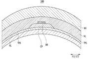
도 1 내지 도 3에 도시된 바와 같이, 본 발명의 일 실시예에 따른 플렉서블 터치 패널(100)은 터치(touch)를 인식하며, 플렉서블 기판(FS), 배선부(WP), 터치 센서부(TS), 윈도우(WI)를 포함한다.1 to 3 , the
플렉서블 기판(FS)은 플렉서블(flexible)하며, 플렉서블 필름을 포함할 수 있다. 플렉서블 기판(FS)은 폴리머, 유리 또는 스테인리스 강 등을 포함하는 절연성 기판이다. 플렉서블 기판(FS)은 플렉서블(flexible)하나, 이에 한정되지 않고 스트레처블(stretchable)하거나, 폴더블(foldable)하거나, 벤더블(bendable)하거나, 롤러블(rollable)할 수 있다. 플렉서블 기판(FS)이 플렉서블(flexible)하거나, 스트렛쳐블(stretable)하거나, 폴더블(foldable)하거나, 벤더블(bendable)하거나, 롤러블(rollable)함으로써, 플렉서블 터치 패널(100) 전체가 플렉서블(flexible)하거나, 스트레처블(stretchable)하거나, 폴더블(foldable)하거나, 벤더블(bendable)하거나, 롤러블(rollable)할 수 있다. 플렉서블 기판(FS)은 일 방향으로 휘어질 수 있으며, 본 발명의 일 실시예에서 플렉서블 기판(FS)은 일 방향인 제1 방향으로 휘어질 수 있다.The flexible substrate FS is flexible and may include a flexible film. The flexible substrate FS is an insulating substrate including a polymer, glass, stainless steel, or the like. The flexible substrate FS is flexible, but is not limited thereto, and may be stretchable, foldable, bendable, or rollable. When the flexible substrate FS is flexible, stretchable, foldable, bendable, or rollable, the entire
플렉서블 터치 패널(100)은 도시하지 않은 터치 제어부를 포함할 수 있으며, 이 터치 제어부는 연성인쇄회로기판 또는 인쇄회로기판 등의 형태로 형성되어 배선부(WP)와 연결될 수 있다. 터치 제어부는 플렉서블 터치 패널(100)로부터 전송된 전기적인 아날로그 신호를 컨버터 등을 통해 디지털 신호로 수치화하여 사용자가 터치한 위치 정보를 계산할 수 있다.The
한편, 본 발명의 일 실시예에서 제1 방향은 플렉서블 기판(FS)이 휘어지는 방향과 동일하나, 본 발명의 다른 실시예에서 제1 방향은 플렉서블 기판(FS)이 휘어지는 방향과 나란할 수 있다.Meanwhile, in one embodiment of the present invention, the first direction is the same as the bending direction of the flexible substrate FS, but in another embodiment of the present invention, the first direction may be parallel to the bending direction of the flexible substrate FS.
배선부(WP)는 플렉서블 기판(FS)의 외곽 영역에 위치하고 있으며, 터치 센서부(TS)와 연결되어 있다. 배선부(WP)는 터치 센서부(TS)와 터치 제어부 사이를 연결할 수 있으며, 금속 등의 불투명 도전성 재료 또는 투명 도전성 재료를 포함할 수 있다. 배선부(WP)는 터치 센서부(TS)와 다른 공정 또는 동일한 공정을 이용해 플렉서블 기판(FS) 상에 형성될 수 있다.The wiring unit WP is located in an outer region of the flexible substrate FS and is connected to the touch sensor unit TS. The wiring unit WP may connect between the touch sensor unit TS and the touch control unit, and may include an opaque conductive material such as a metal or a transparent conductive material. The wiring unit WP may be formed on the flexible substrate FS using a process different from or the same as that of the touch sensor unit TS.
터치 센서부(TS)는 터치를 직접적으로 인식하는 부분이며, 전체적으로 투명하게 형성되어 있다. 터치 센서부(TS)는 플렉서블 기판(FS) 상에 위치하여 정전 용량식으로 이루어질 수 있다.The touch sensor unit TS is a part that directly recognizes a touch, and is entirely transparent. The touch sensor unit TS may be positioned on the flexible substrate FS and formed of a capacitive type.
터치 센서부(TS)는 플렉서블 기판(FS) 상에서 제1 방향으로 연장되어 배선부(WP)와 연결된 제1 신호 라인(SL1), 제1 방향과 교차하는 제2 방향으로 연장되어 배선부(WP)와 연결된 제2 신호 라인(SL2), 제1 신호 라인(SL1)과 제2 신호 라인(SL2)이 교차하는 부분에 대응하여 제1 신호 라인(SL1)과 제2 신호 라인(SL2) 사이에 위치하는 절연 패턴(IP)을 포함한다.The touch sensor unit TS extends in a first direction on the flexible substrate FS and extends in a second direction crossing the first signal line SL1 connected to the wiring unit WP and the wiring unit WP. ) between the first signal line SL1 and the second signal line SL2 corresponding to the intersection of the second signal line SL2 and the first signal line SL1 and the second signal line SL2 . and an insulating pattern (IP) positioned thereon.
제1 신호 라인(SL1)은 복수이며, 복수의 제1 신호 라인(SL1)들 각각은 제2 방향으로 순차적으로 배치될 수 있다.A plurality of first signal lines SL1 may be provided, and each of the plurality of first signal lines SL1 may be sequentially disposed in the second direction.
제2 신호 라인(SL2)은 복수이며, 복수의 제2 신호 라인(SL2)들 각각은 제1 방향으로 순차적으로 배치될 수 있다.A plurality of second signal lines SL2 may be provided, and each of the plurality of second signal lines SL2 may be sequentially disposed in a first direction.
제1 신호 라인(SL1)과 제2 신호 라인(SL2)은 서로 교차하며, 제1 신호 라인(SL1)과 제2 신호 라인(SL2)이 교차하는 부분에는 제1 신호 라인(SL1)과 제2 신호 라인(SL2)이 절연 교차되도록 제1 신호 라인(SL1)과 제2 신호 라인(SL2) 사이에 절연 패턴(IP)이 위치하고 있다.The first signal line SL1 and the second signal line SL2 intersect each other, and the first signal line SL1 and the second signal line SL2 intersect at the intersection of the first signal line SL1 and the second signal line SL2 . The insulating pattern IP is positioned between the first signal line SL1 and the second signal line SL2 so that the signal line SL2 is insulated and crossed.
이와 같이 구성된 플렉서블 터치 패널(100)에서, 복수의 제1 신호 라인(SL1)과 복수의 제2 신호 라인(SL2)에 순차적으로 전압이 인가되어 제1 신호 라인(SL1) 및 제2 신호 라인(SL2) 각각에 전하가 충진될 때, 제1 신호 라인(SL1) 또는 제2 신호 라인(SL2)에 터치가 수행되면, 터치가 수행된 제1 신호 라인(SL1) 또는 제2 신호 라인(SL2)의 정전 용량이 변화되어 어느 위치에 터치가 수행 되었는지를 확인할 수 있다.In the
이하, 제1 신호 라인(SL1), 제2 신호 라인(SL2), 절연 패턴(IP) 각각에 대해 구체적으로 설명한다.Hereinafter, each of the first signal line SL1 , the second signal line SL2 , and the insulating pattern IP will be described in detail.
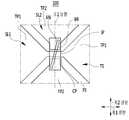
제1 신호 라인(SL1)은 제1 터치 패드부(TP1) 및 연결부(CP)를 포함한다.The first signal line SL1 includes a first touch pad part TP1 and a connection part CP.
제1 터치 패드부(TP1)는 복수이며, 복수의 제1 터치 패드부(TP1)들 각각은 플렉서블 기판(FS)이 휘어지는 방향인 제1 방향으로 상호 이격되어 배치되어 있다. 연결부(CP)는 복수의 제1 터치 패드부(TP1) 각각의 사이를 연결하며, 구체적으로 이웃하는 제1 터치 패드부(TP1) 사이를 연결하고 있다. 제1 터치 패드부(TP1) 및 연결부(CP)는 일체로 형성되어 있다. 제1 터치 패드부(TP1) 및 연결부(CP)는 인듐틴옥사이드(ITO), 인듐징크옥사이드(IZO), 메탈 메쉬(metal mesh), 도전성 고분자 및 은나노와이어(AgNW) 중 하나 이상을 포함하는 투명 도전 물질을 포함할 수 있다. 여기서, 메탈 메쉬는 복수의 개구부가 형성된 메쉬(mesh) 형태의 금속 패턴층을 의미하며, 메탈 메쉬는 메쉬 형태를 가질 수 있다면 어떠한 형태의 개구부도 포함할 수 있다. 또한, 은나노와이어는 수지 등을 포함하는 기재층 내부에 분산된 형태를 가질 수 있으나, 이에 한정되지 않고 은나노와이어를 포함한다면 어떠한 형태로도 형성될 수 있다.A plurality of first touch pad units TP1 is provided, and each of the plurality of first touch pad units TP1 is disposed to be spaced apart from each other in a first direction in which the flexible substrate FS is bent. The connection part CP connects between each of the plurality of first touch pad parts TP1 , specifically, between adjacent first touch pad parts TP1 . The first touch pad part TP1 and the connection part CP are integrally formed. The first touch pad part TP1 and the connection part CP are transparent including at least one of indium tin oxide (ITO), indium zinc oxide (IZO), a metal mesh, a conductive polymer, and a silver nanowire (AgNW) It may include a conductive material. Here, the metal mesh means a metal pattern layer in the form of a mesh in which a plurality of openings are formed, and the metal mesh may include any type of opening if it can have a mesh shape. In addition, the silver nanowires may have a form dispersed inside the base layer including a resin, etc., but is not limited thereto and may be formed in any form as long as the silver nanowires are included.
제2 신호 라인(SL2)은 제2 터치 패드부(TP2) 및 브릿지(BR)를 포함한다.The second signal line SL2 includes the second touch pad unit TP2 and the bridge BR.
제2 터치 패드부(TP2)는 복수이며, 복수의 제2 터치 패드부(TP2)들 각각은 플렉서블 기판(FS)이 휘어진 방향인 제1 방향과 교차하는 제2 방향으로 상호 이격되어 배치되어 있다. 브릿지(BR)는 복수의 제2 터치 패드부(TP2) 각각의 사이를 연결하며, 구체적으로 이웃하는 제2 터치 패드부(TP2) 사이를 연결하고 있다. 제2 터치 패드부(TP2) 및 브릿지(BR)는 서로 다른 층으로 형성되어 있다. 브릿지(BR)는 브릿지(bridge) 형태를 가지고 이웃하는 제2 터치 패드부(TP2) 사이를 연결하며, 구체적으로 절연 패턴(IP)에 의해 연결부(CP)와 이격되어 이웃하는 제2 터치 패드부(TP2) 사이를 연결한다.A plurality of second touch pad units TP2 is provided, and each of the plurality of second touch pad units TP2 is disposed to be spaced apart from each other in a second direction intersecting the first direction in which the flexible substrate FS is bent. . The bridge BR connects between each of the plurality of second touch pad units TP2 , specifically, between adjacent second touch pad units TP2 . The second touch pad unit TP2 and the bridge BR are formed of different layers. The bridge BR has a bridge shape and connects the adjacent second touch pad units TP2, and specifically, the second touch pad unit adjacent to the connecting unit CP is spaced apart from the connecting unit CP by the insulating pattern IP. (TP2) is connected.
제2 터치 패드부(TP2)는 제1 터치 패드부(TP1) 및 연결부(CP)와 동일한 층에 형성되는 동시에 동일한 재료를 포함하며, 제1 터치 패드부(TP1) 및 연결부(CP)와 동시에 형성될 수 있다. 제2 터치 패드부(TP2)는 인듐틴옥사이드(ITO), 인듐징크옥사이드(IZO), 메탈 메쉬(metal mesh), 도전성 고분자, 탄소나노튜브 (CNT), 은나노와이어(AgNW) 중 하나 이상을 포함하는 투명 도전 물질을 포함할 수 있다.The second touch pad unit TP2 is formed on the same layer as the first touch pad unit TP1 and the connection unit CP and includes the same material, and is formed at the same time as the first touch pad unit TP1 and the connection unit CP. can be formed. The second touch pad unit TP2 includes at least one of indium tin oxide (ITO), indium zinc oxide (IZO), metal mesh, conductive polymer, carbon nanotube (CNT), and silver nanowire (AgNW). and a transparent conductive material.
브릿지(BR)는 절연 패턴(IP)을 사이에 두고 연결부(CP)와 이격되어 위치하고 있으며, 구체적으로 절연 패턴(IP)을 사이에 두고 연결부(CP) 상에 위치하고 있다. 브릿지(BR)는 제2 터치 패드부(TP2)와는 다른 재료를 포함하며, 일례로 전기 저항이 낮은 금, 은, 구리 등의 금속을 포함할 수 있다.The bridge BR is positioned to be spaced apart from the connection part CP with the insulating pattern IP interposed therebetween, and is specifically positioned on the connection part CP with the insulating pattern IP interposed therebetween. The bridge BR may include a material different from that of the second touch pad part TP2 , and may include, for example, a metal having a low electrical resistance, such as gold, silver, or copper.
한편, 본 발명의 일 실시예에서, 브릿지(BR)는 금속을 포함하나, 이에 한정되지 않고 본 발명의 다른 실시예에서 브릿지는 인듐틴옥사이드(ITO), 인듐징크옥사이드(IZO), 메탈 메쉬(metal mesh), 도전성 고분자, 탄소나노튜브 (CNT), 은나노와이어(AgNW) 등 중 하나 이상을 포함할 수 있다.On the other hand, in one embodiment of the present invention, the bridge (BR) includes a metal, but is not limited thereto. In another embodiment of the present invention, the bridge is indium tin oxide (ITO), indium zinc oxide (IZO), a metal mesh ( metal mesh), conductive polymers, carbon nanotubes (CNT), silver nanowires (AgNW), and the like.
브릿지(BR)는 플렉서블 기판(FS)이 휘어진 방향과 교차하는 방향인 제2 방향으로 연장되어 이웃하는 제2 터치 패드부(TP2) 사이를 연결하고 있다. 브릿지(BR)의 연장 방향은 플렉서블 기판(FS)이 휘어지는 방향인 제1 방향과 수직인 제2 방향으로 연장되어 있으나, 이에 한정되지 않고 브릿지(BR)의 연장 방향은 플렉서블 기판(FS)이 휘어지는 방향과 교차한다면 어떠한 방향으로도 연장될 수 있다. 브릿지(BR)는 굴곡된 표면을 가지는 절연 패턴(IP) 상에 위치하며, 이로 인해 브릿지(BR)는 절연 패턴(IP)의 굴곡된 표면을 따라 제2 방향으로 굴곡되어 있다. 브릿지(BR)가 절연 패턴(IP)의 굴곡된 표면을 따라 제2 방향으로 굴곡되어 있음으로써, 브릿지(BR)의 굴곡진 여러 부분들에는 잔류 응력(residual stress)이 존재하기 때문에, 제2 방향으로 스트레스가 발생될 경우 스트레스에 의해 파괴될 가능성이 크다. 그러나, 플렉서블 기판(FS)이 제1 방향으로 휘어지고 브릿지(BR)가 제1 방향과 교차하는 제2 방향으로 연장됨으로써, 플렉서블 기판(FS)의 휘어짐에 따라 브릿지(BR)에 제1 방향으로 스트레스가 인가되기 때문에, 스트레스에 의해 브릿지(BR)가 파괴되는 것이 억제된다.The bridge BR extends in a second direction that intersects the direction in which the flexible substrate FS is bent to connect the adjacent second touch pad units TP2. The extension direction of the bridge BR extends in a second direction perpendicular to the first direction, which is a direction in which the flexible substrate FS is bent, but is not limited thereto, and the extension direction of the bridge BR is a direction in which the flexible substrate FS is bent. It can extend in any direction if it intersects the direction. The bridge BR is positioned on the insulating pattern IP having a curved surface, so that the bridge BR is curved in the second direction along the curved surface of the insulating pattern IP. Since the bridge BR is curved in the second direction along the curved surface of the insulating pattern IP, residual stress exists in various curved portions of the bridge BR, so that in the second direction When stress occurs, it is highly likely to be destroyed by the stress. However, as the flexible substrate FS is bent in the first direction and the bridge BR extends in a second direction intersecting the first direction, the flexible substrate FS is bent in the first direction to the bridge BR in the first direction. Since the stress is applied, it is suppressed that the bridge BR is destroyed by the stress.
또한, 브릿지(BR)가 제1 방향과 교차하는 제2 방향으로 연장됨으로써, 플렉서블 기판(FS)의 휘어짐에 따라 브릿지(BR)에 제1 방향으로 스트레스가 발생되더라도, 종횡비가 큰 브릿지(BR)에 횡 방향인 제1 방향으로 스트레스가 인가되기 때문에, 제1 방향으로 인가되는 스트레스에 의해 브릿지(BR)가 파괴되는 것이 억제된다.In addition, since the bridge BR extends in the second direction intersecting the first direction, even if stress is generated in the bridge BR in the first direction due to the bending of the flexible substrate FS, the bridge BR having a large aspect ratio Since the stress is applied in the first direction, which is the transverse direction, the bridge BR is suppressed from being destroyed by the stress applied in the first direction.
절연 패턴(IP)은 연결부(CP)와 브릿지(BR) 사이에 위치하고 있으며, 섬(island) 형태의 패턴으로 형성되어 있다. 절연 패턴(IP)은 연결부(CP)를 덮고 있다. 절연 패턴(IP)은 굴곡된 표면을 가지며, 이러한 굴곡된 표면 상에 브릿지(BR)가 위치함으로써, 브릿지(BR)는 절연 패턴(IP)의 굴곡된 표면을 따라 굴곡되어 연장된다. 절연 패턴(IP)은 SiNx, Al2O3, SiO2, TiO2 등 중 어느 하나 이상을 포함하거나, 고분자를 포함할 수 있다.The insulating pattern IP is positioned between the connection part CP and the bridge BR, and is formed in an island-shaped pattern. The insulating pattern IP covers the connection part CP. The insulating pattern IP has a curved surface, and when the bridge BR is positioned on the curved surface, the bridge BR is curved and extended along the curved surface of the insulating pattern IP. The insulating pattern IP may includeany one or more of SiNx, Al 2 O3 , SiO2 , TiO2 , or a polymer.
한편, 본 발명의 일 실시예에서 절연 패턴(IP)은 섬(island) 형태의 절연 패턴으로 형성되나, 본 발명의 다른 실시예에서 절연 패턴(IP)은 하나의 판 형태의 절연층으로 형성될 수 있다.Meanwhile, in an embodiment of the present invention, the insulating pattern IP is formed as an island-shaped insulating pattern, but in another embodiment of the present invention, the insulating pattern IP is formed as a single plate-shaped insulating layer. can
이상과 같은 터치 센서부(TS) 상에 윈도우(WI)가 위치하고 있다.The window WI is positioned on the touch sensor unit TS as described above.
윈도우(WI)는 점탄성(viscoelastic) 물질을 포함하는 접착층(VL)에 의해 터치 센서부(TS)에 부착될 수 있으며, 터치 센서부(TS) 상에 위치하여 외부의 간섭으로부터 터치 센서부(TS)를 보호하는 역할을 한다. 윈도우(WI)는 터치 센서부(TS) 및 배선부(WP)가 형성된 플렉서블 기판(FS)보다 큰 면적을 가질 수 있다. 윈도우(WI)는 터치 센서부(TS) 상에 위치하며, 플렉서블 기판(FS)이 휘어진 방향과 동일한 방향으로 휘어져 있다. 윈도우(WI)는 플렉서블 기판(FS)이 휘어진 방향과 동일한 방향인 제1 방향으로 휘어진 상태를 유지할 수 있으며, 이로 인해 플렉서블 기판(FS)도 제1 방향으로 휘어진 상태를 유지할 수 있다. 윈도우(WI)는 투명한 물질을 포함할 수 있으며, 일례로 고분자(polymer), 유리(glass), 쿼츠(quartz), 사파이어(sapphire) 등 중 하나 이상을 포함할 수 있다.The window WI may be attached to the touch sensor unit TS by an adhesive layer VL including a viscoelastic material, and is positioned on the touch sensor unit TS to protect the touch sensor unit TS from external interference. ) to protect The window WI may have a larger area than the flexible substrate FS on which the touch sensor unit TS and the wiring unit WP are formed. The window WI is positioned on the touch sensor unit TS and is curved in the same direction as the curved direction of the flexible substrate FS. The window WI may maintain a curved state in the first direction, which is the same direction as that of the flexible substrate FS, and thus the flexible substrate FS may also maintain a curved state in the first direction. The window WI may include a transparent material, and may include, for example, one or more of a polymer, glass, quartz, sapphire, and the like.
이와 같이, 본 발명의 일 실시예에 따른 플렉서블 터치 패널(100)은 브릿지(BR)가 플렉서블 기판(FS)이 휘어진 방향인 제1 방향과 교차하는 제2 방향으로 연장됨으로써, 플렉서블 기판(FS)이 제1 방향으로 휘어짐에 따라 브릿지(BR)에 제1 방향으로 스트레스가 발생되더라도, 종횡비가 큰 브릿지(BR)에 횡 방향인 제1 방향으로 스트레스가 인가되기 때문에, 제1 방향으로 인가되는 스트레스에 의해 브릿지(BR)가 파괴되는 것이 억제된다.As described above, in the
또한, 본 발명의 일 실시예에 따른 플렉서블 터치 패널(100)은 브릿지(BR)가 절연 패턴(IP)의 굴곡된 표면을 따라 제2 방향으로 굴곡 연장되어 브릿지(BR)의 굴곡진 여러 부분들에 잔류 응력(residual stress)이 존재하더라도, 플렉서블 기판(FS)이 제1 방향으로 휘어져 브릿지(BR)에 제1 방향으로 스트레스가 인가되기 때문에, 스트레스에 의해 브릿지(BR)가 파괴되는 것이 억제된다.In addition, in the
즉, 스트레스(stress)에 의한 터치 센서부(TS)의 브릿지(BR)의 파손이 억제된 플렉서블 터치 패널(100)이 제공된다.That is, the
이하, 도 4를 참조하여 본 발명의 다른 실시예에 따른 플렉서블 터치 패널을 설명한다. 이하에서는 상술한 본 발명의 일 실시예에 따른 플렉서블 터치 패널과 다른 부분에 대해서 설명한다.Hereinafter, a flexible touch panel according to another embodiment of the present invention will be described with reference to FIG. 4 . Hereinafter, parts different from the flexible touch panel according to an embodiment of the present invention will be described.
도 4는 본 발명의 다른 실시예에 따른 플렉서블 터치 패널의 일 부분을 나타낸 평면도이다.4 is a plan view illustrating a portion of a flexible touch panel according to another embodiment of the present invention.
도 4에 도시된 바와 같이, 본 발명의 다른 실시예에 따른 플렉서블 터치 패널(100)의 브릿지(BR)는 복수이며, 복수의 브릿지(BR)들은 제2 방향으로 연장되어 이웃하는 제2 터치 패드부(TP2) 사이를 연결하고 있다.As shown in FIG. 4 , a plurality of bridges BR of the
이와 같이, 본 발명의 다른 실시예에 따른 플렉서블 터치 패널(100)은 복수의 브릿지(BR)들이 플렉서블 기판(FS)이 휘어진 방향인 제1 방향과 교차하는 제2 방향으로 연장됨으로써, 플렉서블 기판(FS)이 제1 방향으로 휘어짐에 따라 복수의 브릿지(BR)들에 제1 방향으로 스트레스가 발생되더라도, 종횡비가 큰 브릿지(BR) 각각에 횡 방향인 제1 방향으로 스트레스가 인가되기 때문에, 제1 방향으로 인가되는 스트레스에 의해 복수의 브릿지(BR)들이 파괴되는 것이 억제된다.As described above, in the
나아가, 본 발명의 다른 실시예에 따른 플렉서블 터치 패널(100)은 브릿지(BR)가 복수로 형성됨으로써, 혹 제1 방향으로 인가되는 스트레스에 의해 복수의 브릿지(BR)들 중 어느 하나가 파괴되더라도 나머지 브릿지(BR)가 존재하기 때문에, 브릿지(BR)의 파손에 의해 이웃하는 제2 터치 패드부(TP2) 사이의 연결이 분리되는 것이 억제된다.Furthermore, in the
즉, 스트레스(stress)에 의한 터치 센서부(TS)의 브릿지(BR)의 파손이 억제된 플렉서블 터치 패널(100)이 제공된다.That is, the
이하, 도 5를 참조하여 본 발명의 다른 실시예에 따른 플렉서블 터치 패널을 설명한다. 이하에서는 상술한 본 발명의 일 실시예에 따른 플렉서블 터치 패널과 다른 부분에 대해서 설명한다.Hereinafter, a flexible touch panel according to another embodiment of the present invention will be described with reference to FIG. 5 . Hereinafter, parts different from the flexible touch panel according to an embodiment of the present invention will be described.
도 5는 본 발명의 다른 실시예에 따른 플렉서블 터치 패널의 일 부분을 나타낸 평면도이다.5 is a plan view illustrating a portion of a flexible touch panel according to another embodiment of the present invention.
도 5에 도시된 바와 같이, 본 발명의 다른 실시예에 따른 플렉서블 터치 패널(100)의 브릿지(BR)의 연장 방향은 제2 방향과 설정된 각도로 틸트(tilt)되어 있다. 브릿지(BR)의 연장 방향은 제2 방향과 5도 내지 80도의 교각(AN)을 형성한다.As shown in FIG. 5 , the extension direction of the bridge BR of the
이와 같이, 본 발명의 다른 실시예에 따른 플렉서블 터치 패널(100)은 브릿지(BR)가 플렉서블 기판(FS)이 휘어진 방향인 제1 방향과 교차하는 방향으로 연장됨으로써, 플렉서블 기판(FS)이 제1 방향으로 휘어짐에 따라 복수의 브릿지(BR)들에 제1 방향으로 스트레스가 발생되더라도, 종횡비가 큰 브릿지(BR) 각각에 횡 방향인 제1 방향으로 스트레스가 인가되기 때문에, 제1 방향으로 인가되는 스트레스에 의해 복수의 브릿지(BR)들이 파괴되는 것이 억제된다.As described above, in the
나아가, 본 발명의 다른 실시예에 따른 플렉서블 터치 패널(100)은 브릿지(BR)가 제2 방향과 설정된 각도로 틸트되어 있음으로써, 브릿지(BR)에 빛이 정면으로 반사되는 것이 억제되기 때문에, 브릿지(BR)가 외부에 시인되는 것이 억제된다.Furthermore, in the
즉, 스트레스(stress)에 의한 터치 센서부(TS)의 브릿지(BR)의 파손이 억제된 플렉서블 터치 패널(100)이 제공된다.That is, the
이하, 도 6을 참조하여 본 발명의 다른 실시예에 따른 플렉서블 표시 장치를 설명한다. 이하에서는 상술한 본 발명의 일 실시예에 따른 플렉서블 터치 패널과 다른 부분에 대해서 설명한다.Hereinafter, a flexible display device according to another exemplary embodiment of the present invention will be described with reference to FIG. 6 . Hereinafter, parts different from the flexible touch panel according to an embodiment of the present invention will be described.
도 6은 본 발명의 다른 실시예에 따른 플렉서블 표시 장치의 일 부분을 나타낸 단면도이다.6 is a cross-sectional view illustrating a portion of a flexible display device according to another exemplary embodiment.
도 6에 도시된 바와 같이, 본 발명의 다른 실시예에 따른 플렉서블 표시 장치(1000)는 이미지를 표시하는 플렉서블 표시 패널(FD), 터치 센서부(TS), 윈도우(WI)를 포함한다.As shown in FIG. 6 , the
플렉서블 표시 패널(FD)은 제1 방향으로 휘어져 있으며, 기판(SUB), 표시부(DM), 밀봉부(EN)를 포함한다.The flexible display panel FD is curved in the first direction and includes a substrate SUB, a display unit DM, and an encapsulation unit EN.
기판(SUB)은 유리, 폴리머 또는 스테인리스 강 등을 포함하는 절연성 기판이다. 기판(SUB)은 플렉서블(flexible)하거나, 스트렛쳐블(stretable)하거나, 폴더블(foldable)하거나, 벤더블(bendable)하거나, 롤러블(rollable)할 수 있다. 기판(SUB)이 플렉서블(flexible)하거나, 스트렛쳐블(stretable)하거나, 폴더블(foldable)하거나, 벤더블(bendable)하거나, 롤러블(rollable)함으로써, 플렉서블 표시 패널(FD) 전체가 플렉서블(flexible)하거나, 스트렛쳐블(stretable)하거나, 폴더블(foldable)하거나, 벤더블(bendable)하거나, 롤러블(rollable)할 수 있다. 일례로, 기판(SUB)은 폴리이미드 등의 수지를 포함하는 플렉서블 필름(film) 형태를 가질 수 있다.The substrate SUB is an insulating substrate including glass, polymer, stainless steel, or the like. The substrate SUB may be flexible, stretchable, foldable, bendable, or rollable. When the substrate SUB is flexible, stretchable, foldable, bendable, or rollable, the entire flexible display panel FD is flexible ( flexible), stretchable, foldable, bendable, or rollable. For example, the substrate SUB may have a flexible film shape including a resin such as polyimide.
표시부(DM)는 복수의 화소를 이용해 이미지를 표시한다. 여기서, 화소란 이미지를 표시하는 최소 단위를 의미할 수 있다. 표시부(DM)는 빛을 발광하는 유기 발광 소자(OLED) 및 유기 발광 소자(OLED)와 연결된 박막 트랜지스터(TFT)를 포함한다. 한편, 본 발명의 다른 실시예에서는 설명의 편의를 위해 표시부(DM)가 유기 발광 소자(OLED) 및 박막 트랜지스터(TFT)를 포함하는 것으로 설명하였으나, 이에 한정되지 않고 표시부(DM)는 하나 이상의 스캔 배선, 하나 이상의 데이터 배선, 복수의 박막 트랜지스터, 하나 이상의 커패시터를 더 포함할 수 있으며, 이러한 구성들은 공지된 다양한 구조를 가질 수 있다The display unit DM displays an image using a plurality of pixels. Here, the pixel may mean a minimum unit for displaying an image. The display unit DM includes an organic light emitting diode (OLED) emitting light and a thin film transistor (TFT) connected to the organic light emitting diode (OLED). Meanwhile, in another embodiment of the present invention, it has been described that the display unit DM includes an organic light emitting diode (OLED) and a thin film transistor (TFT) for convenience of explanation, but the present invention is not limited thereto and the display unit DM includes one or more scans. It may further include a wiring line, one or more data wiring lines, a plurality of thin film transistors, and one or more capacitors, and these components may have various known structures.
박막 트랜지스터(TFT)는 액티브층(AL), 게이트 전극(GE), 소스 전극(SE) 및 드레인 전극(DE)을 포함한다.The thin film transistor TFT includes an active layer AL, a gate electrode GE, a source electrode SE, and a drain electrode DE.
액티브층(AL)은 폴리 실리콘 또는 산화물 반도체로 이루어질 수 있다. 산화물 반도체는 티타늄(Ti), 하프늄(Hf), 지르코늄(Zr), 알루미늄(Al), 탄탈륨(Ta), 게르마늄(Ge), 아연(Zn), 갈륨(Ga), 주석(Sn) 또는 인듐(In)을 기본으로 하는 산화물, 이들의 복합 산화물인 산화아연(ZnO), 인듐-갈륨-아연 산화물(InGaZnO4), 인듐-아연 산화물(Zn-In-O), 아연-주석 산화물(Zn-Sn-O) 인듐-갈륨 산화물 (In-Ga-O), 인듐-주석 산화물(In-Sn-O), 인듐-지르코늄 산화물(In-Zr-O), 인듐-지르코늄-아연 산화물(In-Zr-Zn-O), 인듐-지르코늄-주석 산화물(In-Zr-Sn-O), 인듐-지르코늄-갈륨 산화물(In-Zr-Ga-O), 인듐-알루미늄 산화물(In-Al-O), 인듐-아연-알루미늄 산화물(In-Zn-Al-O), 인듐-주석-알루미늄 산화물(In-Sn-Al-O), 인듐-알루미늄-갈륨 산화물(In-Al-Ga-O), 인듐-탄탈륨 산화물(In-Ta-O), 인듐-탄탈륨-아연 산화물(In-Ta-Zn-O), 인듐-탄탈륨-주석 산화물(In-Ta-Sn-O), 인듐-탄탈륨-갈륨 산화물(In-Ta-Ga-O), 인듐-게르마늄 산화물(In-Ge-O), 인듐-게르마늄-아연 산화물(In-Ge-Zn-O), 인듐-게르마늄-주석 산화물(In-Ge-Sn-O), 인듐-게르마늄-갈륨 산화물(In-Ge-Ga-O), 티타늄-인듐-아연 산화물(Ti-In-Zn-O), 하프늄-인듐-아연 산화물(Hf-In-Zn-O) 중 어느 하나를 포함할 수 있다.The active layer AL may be made of polysilicon or an oxide semiconductor. Oxide semiconductors are titanium (Ti), hafnium (Hf), zirconium (Zr), aluminum (Al), tantalum (Ta), germanium (Ge), zinc (Zn), gallium (Ga), tin (Sn), or indium ( oxides based on In), their complex oxides such as zinc oxide (ZnO), indium-gallium-zinc oxide (InGaZnO4), indium-zinc oxide (Zn-In-O), zinc-tin oxide (Zn-Sn- O) indium-gallium oxide (In-Ga-O), indium-tin oxide (In-Sn-O), indium-zirconium oxide (In-Zr-O), indium-zirconium-zinc oxide (In-Zr-Zn) -O), indium-zirconium-tin oxide (In-Zr-Sn-O), indium-zirconium-gallium oxide (In-Zr-Ga-O), indium-aluminum oxide (In-Al-O), indium- Zinc-aluminum oxide (In-Zn-Al-O), indium-tin-aluminum oxide (In-Sn-Al-O), indium-aluminum-gallium oxide (In-Al-Ga-O), indium-tantalum oxide (In-Ta-O), indium-tantalum-zinc oxide (In-Ta-Zn-O), indium-tantalum-tin oxide (In-Ta-Sn-O), indium-tantalum-gallium oxide (In-Ta -Ga-O), indium-germanium oxide (In-Ge-O), indium-germanium-zinc oxide (In-Ge-Zn-O), indium-germanium-tin oxide (In-Ge-Sn-O), Any one of indium-germanium-gallium oxide (In-Ge-Ga-O), titanium-indium-zinc oxide (Ti-In-Zn-O), and hafnium-indium-zinc oxide (Hf-In-Zn-O) may include.
액티브층(AL)은 불순물이 도핑되지 않은 채널 영역과, 채널 영역의 양 옆으로 불순물이 도핑되어 형성된 소스 영역 및 드레인 영역을 포함한다. 여기서, 이러한 불순물은 박막 트랜지스터의 종류에 따라 달라지며, N형 불순물 또는 P형 불순물이 가능하다. 액티브층(AL)이 산화물 반도체로 이루어지는 경우에는 고온에 노출되는 등의 외부 환경에 취약한 산화물 반도체를 보호하기 위해 별도의 보호층이 추가될 수 있다.The active layer AL includes a channel region not doped with impurities, and a source region and a drain region formed by doping both sides of the channel region with impurities. Here, the impurity varies depending on the type of the thin film transistor, and may be an N-type impurity or a P-type impurity. When the active layer AL is made of an oxide semiconductor, a separate protective layer may be added to protect the oxide semiconductor that is vulnerable to external environments such as exposure to high temperatures.
게이트 전극(GE)은 일 절연층을 사이에 두고 액티브층(AL) 상에 위치하며, 소스 전극(SE) 및 드레인 전극(DE) 각각은 게이트 전극(GE)을 덮는 타 절연층 상에 위치하여 컨택홀을 통해 액티브층(AL)의 소스 영역 및 드레인 영역 각각과 연결되어 있다. 드레인 전극(DE)은 유기 발광 소자(OLED)의 제1 전극(E1)과 컨택홀을 통해 연결되어 있다.The gate electrode GE is positioned on the active layer AL with one insulating layer interposed therebetween, and each of the source electrode SE and the drain electrode DE is positioned on the other insulating layer covering the gate electrode GE. It is connected to each of the source region and the drain region of the active layer AL through a contact hole. The drain electrode DE is connected to the first electrode E1 of the organic light emitting diode OLED through a contact hole.
유기 발광 소자(OLED)는 박막 트랜지스터(TFT)의 드레인 전극(DE)과 연결된 제1 전극(E1), 제1 전극(E1) 상에 위치하는 유기 발광층(EL), 유기 발광층(EL) 상에 위치하는 제2 전극(E2)을 포함한다.The organic light emitting diode OLED is formed on the first electrode E1 connected to the drain electrode DE of the thin film transistor TFT, the organic light emitting layer EL positioned on the first electrode E1, and the organic light emitting layer EL. and a second electrode E2 positioned thereon.
제1 전극(E1)은 정공 주입 전극인 양극(anode)일 수 있으며, 광 반사성, 광 반투과성, 광 투과성 전극 중 어느 하나의 전극일 수 있다. 한편, 본 발명의 다른 실시예에서 제1 전극(E1)은 전자 주입 전극인 음극(cathode)일 수 있다.The first electrode E1 may be an anode that is a hole injection electrode, and may be any one of a light reflective electrode, a light semitransmissive electrode, and a light transmissive electrode. Meanwhile, in another embodiment of the present invention, the first electrode E1 may be a cathode that is an electron injection electrode.
유기 발광층(EL)은 제1 전극(E1) 상에 위치하고 있다. 유기 발광층(EL)은 저분자 유기물 또는 PEDOT(Poly 3,4-ethylenedioxythiophene) 등의 고분자 유기물로 이루어질 수 있다. 유기 발광층(EL)은 적색을 발광하는 적색 유기 발광층, 녹색을 발광하는 녹색 유기 발광층 및 청색을 발광하는 청색 유기 발광층을 포함할 수 있으며, 적색 유기 발광층, 녹색 유기 발광층 및 청색 유기 발광층은 각각 적색 화소, 녹색 화소 및 청색 화소에 형성되어 컬러 화상을 구현하게 된다. 유기 발광층(EL)은 적색 유기 발광층, 녹색 유기 발광층 및 청색 유기 발광층을 적색 화소, 녹색 화소 및 청색 화소에 모두 함께 적층하고, 각 화소별로 적색 색필터, 녹색 색필터 및 청색 색필터를 형성하여 컬러 화상을 구현할 수 있다. 다른 예로, 유기 발광층(EL)으로서 백색을 발광하는 백색 유기 발광층을 적색 화소, 녹색 화소 및 청색 화소 모두에 형성하고, 각 화소별로 각각 적색 색필터, 녹색 색필터 및 청색 색필터를 형성하여 컬러 화상을 구현할 수도 있다. 유기 발광층(EL)으로서 백색 유기 발광층과 색필터를 이용하여 컬러 화상을 구현하는 경우, 적색 유기 발광층, 녹색 유기 발광층 및 청색 유기 발광층을 각각의 개별 화소 즉, 적색 화소, 녹색 화소 및 청색 화소에 증착하기 위한 증착 마스크를 사용하지 않아도 된다. 다른 예에서 설명한 유기 발광층(EL)으로서 백색 유기 발광층은 하나의 유기 발광층으로 형성될 수 있음은 물론이고, 복수 개의 유기 발광층을 적층하여 백색을 발광할 수 있도록 한 구성까지 포함한다. 일례로, 유기 발광층(EL)은 적어도 하나의 옐로우 유기 발광층과 적어도 하나의 청색 유기 발광층을 조합하여 백색 발광을 가능하게 한 구성, 적어도 하나의 시안 유기 발광층과 적어도 하나의 적색 유기 발광층을 조합하여 백색 발광을 가능하게 한 구성, 적어도 하나의 마젠타 유기 발광층과 적어도 하나의 녹색 유기 발광층을 조합하여 백색 발광을 가능하게 한 구성 등을 포함할 수 있다.The organic light emitting layer EL is positioned on the first electrode E1 . The organic light emitting layer EL may be formed of a low molecular weight organic material or a high molecular weight organic material such as poly 3,4-ethylenedioxythiophene (PEDOT). The organic emission layer EL may include a red organic emission layer that emits red light, a green organic emission layer that emits green light, and a blue organic emission layer that emits blue light, and the red organic emission layer, the green organic emission layer, and the blue organic emission layer are each a red pixel. , is formed in the green pixel and the blue pixel to implement a color image. The organic light emitting layer EL is formed by stacking a red organic light emitting layer, a green organic light emitting layer, and a blue organic light emitting layer together on a red pixel, a green pixel, and a blue pixel, and forming a red color filter, a green color filter and a blue color filter for each pixel. image can be realized. As another example, as the organic light emitting layer EL, a white organic light emitting layer emitting white light is formed in all of the red pixels, green pixels and blue pixels, and a red color filter, a green color filter and a blue color filter are respectively formed for each pixel to form a color image. can also be implemented. When a color image is implemented using a white organic light emitting layer and a color filter as the organic light emitting layer (EL), a red organic light emitting layer, a green organic light emitting layer, and a blue organic light emitting layer are deposited on each individual pixel, that is, a red pixel, a green pixel, and a blue pixel. It is not necessary to use a deposition mask for this purpose. As the organic light emitting layer (EL) described in another example, the white organic light emitting layer may be formed as one organic light emitting layer, and includes a configuration in which a plurality of organic light emitting layers are stacked to emit white light. For example, the organic light emitting layer EL is configured to enable white light emission by combining at least one yellow organic light emitting layer and at least one blue organic light emitting layer, and at least one cyan organic light emitting layer and at least one red organic light emitting layer are combined to produce white light. It may include a configuration that enables light emission, a configuration that enables white light emission by combining at least one magenta organic emission layer and at least one green organic emission layer.
제2 전극(E2)은 유기 발광층(EL) 상에 위치하며, 전자 주입 전극인 음극(cathode)일 수 있다. 제2 전극(E2)은 광 반사성, 광 반투과성, 광 투과성 전극 중 어느 하나의 전극일 수 있다. 제2 전극(E2)은 유기 발광층(EL)을 덮도록 기판(SUB)의 표시 영역(DA) 전체에 걸쳐서 위치하고 있다. 한편, 본 발명의 다른 실시예에서 제2 전극(E2)은 정공 주입 전극인 양극일 수 있다.The second electrode E2 is positioned on the organic light emitting layer EL and may be a cathode that is an electron injection electrode. The second electrode E2 may be any one of a light reflective electrode, a light semitransmissive electrode, and a light transmissive electrode. The second electrode E2 is positioned over the entire display area DA of the substrate SUB to cover the organic light emitting layer EL. Meanwhile, in another embodiment of the present invention, the second electrode E2 may be an anode that is a hole injection electrode.
밀봉부(EN)는 표시부(DM)를 사이에 두고 기판(SUB) 상에 위치하고 있다. 밀봉부(EN)는 기판(SUB)의 표시 영역(DA) 및 비표시 영역(NDA) 전체에 걸쳐서 기판(SUB) 상에 위치하고 있으며, 기판(SUB)과 함께 표시부(DM)를 밀봉하고 있다. 밀봉부(EN)는 박막 밀봉부(thin film encapsulation)로 형성될 수 있다. 밀봉부(EN)는 표시부(DM) 상에 위치하는 유기층(OL) 및 유기층(OL) 상에 위치하는 무기층(IL)을 포함한다. 한편, 본 발명의 또 다른 실시예에서 밀봉부(EN)는 상호 교호적으로 적층된 하나 이상의 유기층 및 하나 이상의 무기층을 포함할 수 있으며, 구체적으로, 무기층 또는 유기층 각각은 복수일 수 있으며, 복수의 무기층 및 복수의 유기층 각각은 상호 교호적으로 적층될 수 있다. 일례로, 밀봉부(EN)는 적어도 2개의 무기층 사이에 적어도 하나의 유기층이 삽입된 샌드위치 구조를 적어도 하나 포함할 수 있다.The encapsulation unit EN is positioned on the substrate SUB with the display unit DM interposed therebetween. The encapsulation unit EN is positioned on the substrate SUB over the entire display area DA and the non-display area NDA of the substrate SUB, and seals the display unit DM together with the substrate SUB. The encapsulation EN may be formed as a thin film encapsulation. The encapsulation part EN includes an organic layer OL positioned on the display part DM and an inorganic layer IL positioned on the organic layer OL. Meanwhile, in another embodiment of the present invention, the encapsulation EN may include one or more organic layers and one or more inorganic layers stacked alternately, and specifically, each of the inorganic layers or the organic layers may be plural, Each of the plurality of inorganic layers and the plurality of organic layers may be alternately stacked. For example, the encapsulation EN may include at least one sandwich structure in which at least one organic layer is inserted between at least two inorganic layers.
유기층(OL)은 고분자로 형성되며, 바람직하게는 폴리에틸렌테레프탈레이트, 폴리이미드, 폴라카보네이트, 에폭시, 폴리에틸렌 및 폴리아크릴레이트 중 어느 하나로 형성되는 단일막 또는 적층막일 수 있다. 일례로, 유기층은 폴리아크릴레이트로 형성될 수 있으며, 구체적으로는 디아크릴레이트계 모노머와 트리아크릴레이트계 모노머를 포함하는 모노머 조성물이 고분자화된 것을 포함한다. 여기서, 모노머 조성물에 모노아크릴레이트계 모노머가 더 포함될 수 있으며, 모노머 조성물에 TPO와 같은 공지의 광개시제가 더욱 포함될 수 있으나 이에 한정되지는 않는다.The organic layer OL is formed of a polymer, and preferably a single film or a laminate film formed of any one of polyethylene terephthalate, polyimide, polycarbonate, epoxy, polyethylene, and polyacrylate. For example, the organic layer may be formed of polyacrylate, and specifically includes a polymerized monomer composition including a diacrylate-based monomer and a triacrylate-based monomer. Here, the monomer composition may further include a monoacrylate-based monomer, and a known photoinitiator such as TPO may be further included in the monomer composition, but is not limited thereto.
무기층(IL)은 금속 산화물 또는 금속 질화물을 포함하는 단일막 또는 적층막일 수 있다. 구체적으로, 무기층은 SiNx, Al2O3, SiO2, TiO2 중 어느 하나 이상을 포함할 수 있다.The inorganic layer IL may be a single layer or a stacked layer including a metal oxide or a metal nitride. Specifically, the inorganic layer may include any one or moreof SiNx, Al 2 O3 , SiO2 , and TiO2 .
본 발명의 다른 실시예에서, 플렉서블 표시 패널(FD)은 유기 발광 소자를 포함하는 유기 발광 표시 장치를 일례로서 설명하나, 본 발명의 또 다른 실시예에 따른 플렉서블 표시 패널은 플렉서블하다면 액정 표시 장치(liquid crystal displays, LCDs), 플라즈마 디스플레이(plasma displays, PDs), 필드에미션디스플레이(field emission displays, FEDs), 전기영동 디스플레이(electrophoretic displays, EPDs), 전기습윤 디스플레이(electrowetting displays, EWDs) 등의 다양한 표시 장치일 수 있다.In another embodiment of the present invention, the flexible display panel FD will be described as an organic light emitting diode display including an organic light emitting device as an example. However, in the flexible display panel according to another embodiment of the present invention, if the flexible display panel FD is flexible, the liquid crystal display device ( liquid crystal displays (LCDs), plasma displays (PDs), field emission displays (FEDs), electrophoretic displays (EPDs), electrowetting displays (EWDs), etc. It may be a display device.
터치 센서부(TS)는 플렉서블 표시 패널(FD)의 밀봉부(EN) 상에 형성되어 있다. 터치 센서부(TS)는 본 발명의 일 실시예에서 상술한 제1 터치 패드부(TP1), 연결부(CP), 제2 터치 패드부, 브릿지(BR)를 포함한다.The touch sensor part TS is formed on the sealing part EN of the flexible display panel FD. The touch sensor unit TS includes the first touch pad unit TP1, the connection unit CP, the second touch pad unit, and the bridge BR, as described above in an embodiment of the present invention.
제1 터치 패드부(TP1), 연결부(CP), 제2 터치 패드부 각각은 밀봉부(EN) 상에 형성되어 있다.Each of the first touch pad part TP1 , the connection part CP, and the second touch pad part is formed on the sealing part EN.
브릿지(BR)는 플렉서블 표시 패널(FD)이 휘어진 방향과 교차하는 방향인 제1 방향으로 연장되어 이웃하는 제2 터치 패드부 사이를 연결하고 있다. 브릿지(BR)의 연장 방향은 플렉서블 표시 패널(FD)이 휘어지는 방향인 제1 방향과 수직인 제2 방향으로 연장되어 있으나, 이에 한정되지 않고 브릿지(BR)의 연장 방향은 플렉서블 표시 패널(FD)이 휘어지는 방향과 교차한다면 어떠한 방향으로도 연장될 수 있다.The bridge BR extends in a first direction that intersects a direction in which the flexible display panel FD is bent to connect adjacent second touch pad units. The extension direction of the bridge BR extends in a second direction perpendicular to the first direction in which the flexible display panel FD is bent, but is not limited thereto, and the extension direction of the bridge BR is the flexible display panel FD. It can extend in any direction as long as it intersects this bending direction.
이상과 같은 터치 센서부(TS) 상에 윈도우(WI)가 위치하고 있다.The window WI is positioned on the touch sensor unit TS as described above.
윈도우(WI)는 점탄성(viscoelastic) 물질을 포함하는 접착층(VL)에 의해 터치 센서부(TS)에 부착될 수 있으며, 터치 센서부(TS) 상에 위치하여 외부의 간섭으로부터 터치 센서부(TS) 및 플렉서블 표시 패널(FD)을 보호하는 역할을 한다. 윈도우(WI)는 플렉서블 표시 패널(FD)보다 큰 면적을 가질 수 있다. 윈도우(WI)는 터치 센서부(TS) 상에 위치하며, 플렉서블 표시 패널(FD)이 휘어진 방향과 동일한 방향으로 휘어져 있다. 윈도우(WI)는 플렉서블 표시 패널(FD)이 휘어진 방향과 동일한 방향인 제1 방향으로 휘어진 상태를 유지할 수 있으며, 이로 인해 플렉서블 표시 패널(FD)도 제1 방향으로 휘어진 상태를 유지할 수 있다. 윈도우(WI)는 투명한 물질을 포함할 수 있으며, 일례로 고분자(polymer), 유리(glass), 쿼츠(quartz), 사파이어(sapphire) 등 중 하나 이상을 포함할 수 있다.The window WI may be attached to the touch sensor unit TS by an adhesive layer VL including a viscoelastic material, and is positioned on the touch sensor unit TS to protect the touch sensor unit TS from external interference. ) and the flexible display panel FD. The window WI may have a larger area than the flexible display panel FD. The window WI is positioned on the touch sensor unit TS, and is curved in the same direction as the curved direction of the flexible display panel FD. The window WI may maintain a curved state in the first direction, which is the same direction as that of the flexible display panel FD, and thus the flexible display panel FD may also maintain a curved state in the first direction. The window WI may include a transparent material, and may include, for example, one or more of a polymer, glass, quartz, sapphire, and the like.
이와 같이, 본 발명의 다른 실시예에 따른 플렉서블 표시 장치(1000)는 브릿지(BR)가 플렉서블 표시 패널(FD)이 휘어진 방향인 제1 방향과 교차하는 제2 방향으로 연장됨으로써, 플렉서블 표시 패널(FD)이 제1 방향으로 휘어짐에 따라 브릿지(BR)에 제1 방향으로 스트레스가 발생되더라도, 종횡비가 큰 브릿지(BR)에 횡 방향인 제1 방향으로 스트레스가 인가되기 때문에, 제1 방향으로 인가되는 스트레스에 의해 브릿지(BR)가 파괴되는 것이 억제된다.As described above, in the
즉, 스트레스(stress)에 의한 터치 센서부(TS)의 브릿지(BR)의 파손이 억제된 플렉서블 표시 장치(1000)가 제공된다.That is, the
본 발명을 앞서 기재한 바에 따라 바람직한 실시예를 통해 설명하였지만, 본 발명은 이에 한정되지 않으며 다음에 기재하는 특허청구범위의 개념과 범위를 벗어나지 않는 한, 다양한 수정 및 변형이 가능하다는 것을 본 발명이 속하는 기술 분야에 종사하는 자들은 쉽게 이해할 것이다.Although the present invention has been described through preferred embodiments as described above, the present invention is not limited thereto, and various modifications and variations are possible without departing from the concept and scope of the following claims. Those in the technical field to which it belongs will readily understand.
플렉서블 기판(FS), 브릿지(BR), 터치 센서부(TS)Flexible substrate (FS), bridge (BR), touch sensor unit (TS)
Claims (14)
Translated fromKorean상기 플렉서블 기판 상에 위치하며, 상기 플렉서블 기판이 휘어진 방향과 교차하는 방향으로 연장된 브릿지(bridge)를 포함하는 터치 센서부
를 포함하는 플렉서블 터치 패널.flexible substrate; and
A touch sensor unit positioned on the flexible substrate and including a bridge extending in a direction crossing a direction in which the flexible substrate is bent
A flexible touch panel comprising a.
상기 브릿지의 연장 방향은 상기 플렉서블 기판이 휘어지는 방향과 수직인 플렉서블 터치 패널.In claim 1,
An extension direction of the bridge is perpendicular to a direction in which the flexible substrate is bent.
상기 터치 센서부는,
상기 플렉서블 기판 상에 위치하며, 각각이 제1 방향으로 상호 이격되어 배치된 복수의 제1 터치 패드부;
상기 복수의 제1 터치 패드부 각각의 사이를 연결하는 연결부;
상기 플렉서블 기판 상에 위치하며, 각각이 상기 제1 방향과 교차하는 제2 방향으로 상호 이격되어 배치된 복수의 제2 터치 패드부; 및
상기 연결부를 덮고 있는 절연 패턴
을 더 포함하며,
상기 브릿지는 상기 절연 패턴을 사이에 두고 상기 연결부 상에 위치하며, 상기 복수의 제2 터치 패드부 각각의 사이를 연결하는 플렉서블 터치 패널.In claim 1,
The touch sensor unit,
a plurality of first touch pad units positioned on the flexible substrate and spaced apart from each other in a first direction;
a connection unit connecting each of the plurality of first touch pad units;
a plurality of second touch pad units positioned on the flexible substrate and spaced apart from each other in a second direction intersecting the first direction; and
Insulation pattern covering the connection part
further comprising,
The bridge is positioned on the connection part with the insulating pattern interposed therebetween, and connects each of the plurality of second touch pad parts to a flexible touch panel.
상기 제1 터치 패드부 및 상기 연결부는 일체로 형성된 플렉서블 터치 패널.In claim 3,
The first touch pad part and the connection part are integrally formed with a flexible touch panel.
상기 제2 터치 패드부는 상기 제1 터치 패드부와 동일한 층에 위치하는 플렉서블 터치 패널.In claim 4,
The second touch pad unit is a flexible touch panel positioned on the same layer as the first touch pad unit.
상기 브릿지는 금속을 포함하는 플렉서블 터치 패널.In claim 3,
The bridge is a flexible touch panel comprising a metal.
상기 제2 터치 패드부는 투명 도전 물질을 포함하는 플렉서블 터치 패널.In claim 6,
The second touch pad part is a flexible touch panel including a transparent conductive material.
상기 절연 패턴은 굴곡된 표면을 가지며,
상기 브릿지는 상기 굴곡된 표면을 따라 굴곡된 플렉서블 터치 패널.In claim 3,
The insulating pattern has a curved surface,
The bridge is a flexible touch panel curved along the curved surface.
상기 브릿지는 복수이며,
복수의 상기 브릿지들은 이웃하는 상기 제2 터치 패드부 사이를 연결하는 플렉서블 터치 패널.In claim 3,
The bridge is plural,
A plurality of the bridges connect the adjacent second touch pad units to a flexible touch panel.
상기 브릿지의 연장 방향은 상기 제2 방향과 5도 내지 80도의 교각(angle of intersection)을 형성하는 플렉서블 터치 패널.In claim 3,
An extension direction of the bridge forms an angle of intersection of 5 degrees to 80 degrees with the second direction.
상기 제1 방향은 상기 플렉서블 기판이 휘어진 방향과 나란한 플렉서블 터치 패널.In claim 3,
The first direction is parallel to a direction in which the flexible substrate is bent.
상기 터치 센서부 상에 위치하며, 상기 플렉서블 기판이 휘어진 방향과 동일한 방향으로 휘어진 윈도우를 더 포함하는 플렉서블 터치 패널.In claim 1,
The flexible touch panel is positioned on the touch sensor unit and further includes a window curved in the same direction as the bending direction of the flexible substrate.
상기 플렉서블 표시 패널 상에 형성되며, 상기 플렉서블 표시 패널이 휘어진 방향과 교차하는 방향으로 연장된 브릿지(bridge)를 포함하는 터치 센서부
를 포함하는 플렉서블 표시 장치.a flexible display panel that displays an image; and
The touch sensor unit is formed on the flexible display panel and includes a bridge extending in a direction crossing the bending direction of the flexible display panel;
A flexible display device comprising:
상기 터치 센서부 상에 위치하며, 상기 플렉서블 표시 패널이 휘어진 방향과 동일한 방향으로 휘어진 윈도우를 더 포함하는 플렉서블 표시 장치.In claim 13,
The flexible display device further comprising a window positioned on the touch sensor unit and curved in the same direction as that in which the flexible display panel is curved.
Priority Applications (17)
| Application Number | Priority Date | Filing Date | Title |
|---|---|---|---|
| KR1020150003504AKR102312260B1 (en) | 2015-01-09 | 2015-01-09 | Flexible touch panel and flexible display device |
| US14/880,753US9933886B2 (en) | 2015-01-09 | 2015-10-12 | Flexible touch panel and flexible display device |
| CN202010677291.3ACN111831158B (en) | 2015-01-09 | 2015-12-15 | Flexible touch panel and flexible display device |
| CN201510930836.6ACN105786237B (en) | 2015-01-09 | 2015-12-15 | Flexible touch panels and flexible display devices |
| JP2015249760AJP7092454B2 (en) | 2015-01-09 | 2015-12-22 | Flexible touch panel and flexible display device |
| EP16150565.6AEP3043247B1 (en) | 2015-01-09 | 2016-01-08 | Flexible touch panel and flexible display device |
| EP20167292.0AEP3693839B1 (en) | 2015-01-09 | 2016-01-08 | Flexible touch panel and flexible display device |
| US15/939,612US10585526B2 (en) | 2015-01-09 | 2018-03-29 | Flexible touch panel and flexible display device |
| US16/749,936US11061516B2 (en) | 2015-01-09 | 2020-01-22 | Flexible touch panel and flexible display device |
| US17/358,686US11347358B2 (en) | 2015-01-09 | 2021-06-25 | Flexible touch panel and flexible display device |
| KR1020210132374AKR102436441B1 (en) | 2015-01-09 | 2021-10-06 | Flexible touch panel and flexible display device |
| US17/827,794US11586329B2 (en) | 2015-01-09 | 2022-05-30 | Flexible touch panel and flexible display device |
| KR1020220104871AKR20220121233A (en) | 2015-01-09 | 2022-08-22 | Flexible touch panel and flexible display device |
| US18/111,858US11807487B2 (en) | 2015-01-09 | 2023-02-20 | Flexible touch panel and flexible display device |
| US18/379,031US12216870B2 (en) | 2015-01-09 | 2023-10-11 | Flexible touch panel and flexible display device |
| KR1020240080245AKR102820493B1 (en) | 2015-01-09 | 2024-06-20 | Flexible touch panel and flexible display device |
| KR1020250075580AKR20250091165A (en) | 2015-01-09 | 2025-06-10 | Flexible touch panel and flexible display device |
Applications Claiming Priority (1)
| Application Number | Priority Date | Filing Date | Title |
|---|---|---|---|
| KR1020150003504AKR102312260B1 (en) | 2015-01-09 | 2015-01-09 | Flexible touch panel and flexible display device |
Related Child Applications (1)
| Application Number | Title | Priority Date | Filing Date |
|---|---|---|---|
| KR1020210132374ADivisionKR102436441B1 (en) | 2015-01-09 | 2021-10-06 | Flexible touch panel and flexible display device |
Publications (2)
| Publication Number | Publication Date |
|---|---|
| KR20160086489A KR20160086489A (en) | 2016-07-20 |
| KR102312260B1true KR102312260B1 (en) | 2021-10-13 |
Family
ID=55077434
Family Applications (5)
| Application Number | Title | Priority Date | Filing Date |
|---|---|---|---|
| KR1020150003504AActiveKR102312260B1 (en) | 2015-01-09 | 2015-01-09 | Flexible touch panel and flexible display device |
| KR1020210132374AActiveKR102436441B1 (en) | 2015-01-09 | 2021-10-06 | Flexible touch panel and flexible display device |
| KR1020220104871ACeasedKR20220121233A (en) | 2015-01-09 | 2022-08-22 | Flexible touch panel and flexible display device |
| KR1020240080245AActiveKR102820493B1 (en) | 2015-01-09 | 2024-06-20 | Flexible touch panel and flexible display device |
| KR1020250075580APendingKR20250091165A (en) | 2015-01-09 | 2025-06-10 | Flexible touch panel and flexible display device |
Family Applications After (4)
| Application Number | Title | Priority Date | Filing Date |
|---|---|---|---|
| KR1020210132374AActiveKR102436441B1 (en) | 2015-01-09 | 2021-10-06 | Flexible touch panel and flexible display device |
| KR1020220104871ACeasedKR20220121233A (en) | 2015-01-09 | 2022-08-22 | Flexible touch panel and flexible display device |
| KR1020240080245AActiveKR102820493B1 (en) | 2015-01-09 | 2024-06-20 | Flexible touch panel and flexible display device |
| KR1020250075580APendingKR20250091165A (en) | 2015-01-09 | 2025-06-10 | Flexible touch panel and flexible display device |
Country Status (5)
| Country | Link |
|---|---|
| US (7) | US9933886B2 (en) |
| EP (2) | EP3043247B1 (en) |
| JP (1) | JP7092454B2 (en) |
| KR (5) | KR102312260B1 (en) |
| CN (2) | CN111831158B (en) |
Families Citing this family (53)
| Publication number | Priority date | Publication date | Assignee | Title |
|---|---|---|---|---|
| KR102267357B1 (en) | 2014-12-15 | 2021-06-21 | 삼성디스플레이 주식회사 | Touch sensor device |
| CN108292186B (en)* | 2015-12-11 | 2021-02-09 | 阿尔卑斯阿尔派株式会社 | Electrostatic capacitance type sensor |
| CN108351734B (en)* | 2015-12-11 | 2020-12-01 | 阿尔卑斯阿尔派株式会社 | Capacitive sensor |
| WO2017142078A1 (en)* | 2016-02-18 | 2017-08-24 | 東レ・ダウコーニング株式会社 | Flexible laminate and flexible display using same |
| KR102332579B1 (en)* | 2016-03-31 | 2021-11-29 | 동우 화인켐 주식회사 | Touch sensor |
| JP6695727B2 (en)* | 2016-04-08 | 2020-05-20 | 株式会社ジャパンディスプレイ | Display device |
| KR101776667B1 (en) | 2016-04-15 | 2017-09-19 | 주식회사 지니틱스 | Pressure detecting device using frame of a display module |
| KR101913395B1 (en)* | 2016-07-29 | 2018-10-31 | 삼성디스플레이 주식회사 | Display apparatus |
| KR101904969B1 (en) | 2016-07-29 | 2018-10-10 | 삼성디스플레이 주식회사 | Display device |
| US10430000B2 (en)* | 2016-08-05 | 2019-10-01 | Innolux Corporation | Touch display device |
| CN106206613B (en)* | 2016-08-24 | 2020-12-29 | 昆山工研院新型平板显示技术中心有限公司 | A flexible display substrate and preparation method thereof |
| KR101908982B1 (en)* | 2016-08-31 | 2018-10-17 | 엘지디스플레이 주식회사 | Organic light emitting display with touch sensor and fabricating method thereof |
| KR102614333B1 (en)* | 2016-09-08 | 2023-12-19 | 삼성디스플레이 주식회사 | Display device |
| KR102685973B1 (en)* | 2016-12-14 | 2024-07-19 | 삼성디스플레이 주식회사 | Touch sensor and display device including the same |
| CN108255331B (en)* | 2016-12-29 | 2024-03-08 | 京东方科技集团股份有限公司 | Flexible touch screen, manufacturing method thereof, display screen, manufacturing method thereof and display equipment |
| KR102741702B1 (en) | 2016-12-30 | 2024-12-12 | 엘지디스플레이 주식회사 | Stretchable Touch Screen, Method for Manufacturing the Same, and Display Device Using the Same |
| CN108304086B (en)* | 2017-01-11 | 2020-09-15 | 群创光电股份有限公司 | Touch control display device |
| JP6840554B2 (en)* | 2017-01-30 | 2021-03-10 | 株式会社ジャパンディスプレイ | Detection device and display device |
| CN108695340A (en)* | 2017-04-05 | 2018-10-23 | 上海和辉光电有限公司 | A kind of display panel and display device |
| KR102374561B1 (en) | 2017-06-19 | 2022-03-15 | 삼성디스플레이 주식회사 | Display device and input sensing member |
| KR102346393B1 (en)* | 2017-06-19 | 2022-01-03 | 동우 화인켐 주식회사 | Method for Manufacturing Flexible Display Device Comprising Touch Sensor |
| CN107315507B (en)* | 2017-07-05 | 2020-06-30 | 京东方科技集团股份有限公司 | A flexible touch substrate, a preparation method thereof, and a touch display device |
| CN107329624B (en)* | 2017-07-10 | 2020-01-21 | 上海天马微电子有限公司 | Flexible touch display panel and display device |
| CN109388294B (en)* | 2017-08-11 | 2021-01-22 | 京东方科技集团股份有限公司 | Touch panel and manufacturing method thereof, and touch display device |
| KR102399607B1 (en)* | 2017-08-17 | 2022-05-19 | 삼성디스플레이 주식회사 | Touch sensor and display device having the same |
| CN109426373B (en)* | 2017-08-21 | 2024-08-30 | 京东方科技集团股份有限公司 | Touch panel, manufacturing method thereof and touch display device |
| CN107704120A (en)* | 2017-08-30 | 2018-02-16 | 京东方科技集团股份有限公司 | Flexible touch screen and its manufacture method, flexible display apparatus |
| CN109426389B (en)* | 2017-09-05 | 2021-03-02 | 京东方科技集团股份有限公司 | Touch substrate, preparation method thereof and display panel |
| KR102374755B1 (en)* | 2017-09-27 | 2022-03-15 | 엘지디스플레이 주식회사 | Display device having a touch structure |
| KR102433103B1 (en)* | 2017-10-02 | 2022-08-17 | 삼성디스플레이 주식회사 | Display device |
| KR102375093B1 (en)* | 2017-10-31 | 2022-03-15 | 엘지디스플레이 주식회사 | Stretchable touch display device |
| US20190227646A1 (en)* | 2018-01-25 | 2019-07-25 | Wuhan China Star Optoelectronics Semiconductor Display Technology Co., Ltd. | Touch panel |
| CN108762543B (en)* | 2018-04-19 | 2021-05-11 | 业成科技(成都)有限公司 | Touch screen and touch device using same |
| KR102533131B1 (en)* | 2018-05-08 | 2023-05-18 | 삼성디스플레이 주식회사 | Touch sensing unit and electronic device including the same |
| CN109189265B (en)* | 2018-08-28 | 2021-10-08 | 上海天马微电子有限公司 | A stretchable panel and flexible display device |
| CN109326221B (en)* | 2018-09-25 | 2021-09-28 | 上海天马微电子有限公司 | Display device and tactile feedback display method for display device |
| KR102017767B1 (en)* | 2018-09-28 | 2019-09-04 | 삼성디스플레이 주식회사 | Display device |
| US12287930B2 (en) | 2019-04-24 | 2025-04-29 | Samsung Display Co., Ltd. | Non-rigid device and display device |
| CN110597409B (en)* | 2019-08-12 | 2020-10-16 | 武汉华星光电半导体显示技术有限公司 | Touch structure, touch display panel and touch display device |
| KR102319542B1 (en)* | 2019-08-28 | 2021-11-02 | 삼성디스플레이 주식회사 | Display device |
| KR102151017B1 (en)* | 2019-08-28 | 2020-09-03 | 삼성디스플레이 주식회사 | Display device |
| KR102795209B1 (en)* | 2019-08-30 | 2025-04-14 | 엘지디스플레이 주식회사 | Touch display device |
| KR20210070457A (en)* | 2019-12-04 | 2021-06-15 | 삼성디스플레이 주식회사 | Input sensing unit and display device including the same |
| CN113048140B (en)* | 2019-12-26 | 2022-05-20 | 杭州新剑机器人技术股份有限公司 | Folding screen rotating shaft assembly and electronic equipment comprising same |
| US11079879B1 (en)* | 2020-01-22 | 2021-08-03 | Wuhan China Star Optoelectronics Semiconductor Display Technology Co., Ltd. | Flexible touch display device |
| US11520444B2 (en)* | 2020-04-21 | 2022-12-06 | Samsung Display Co., Ltd. | Display device and method of inspecting the same |
| CN113703598B (en)* | 2020-05-22 | 2025-01-10 | 宸美(厦门)光电有限公司 | Foldable touch display device |
| KR20220022512A (en)* | 2020-08-18 | 2022-02-28 | 삼성디스플레이 주식회사 | Electronic device |
| KR102480860B1 (en)* | 2020-08-27 | 2022-12-26 | 삼성디스플레이 주식회사 | Display device |
| KR20220058699A (en) | 2020-10-29 | 2022-05-10 | 삼성디스플레이 주식회사 | Resin composition, adhesive member, and display device including the same |
| KR20220063812A (en) | 2020-11-09 | 2022-05-18 | 삼성디스플레이 주식회사 | Resin composition, adhesive meber, and display device including the same |
| CN116647975A (en)* | 2022-02-15 | 2023-08-25 | 群创光电股份有限公司 | electronic device |
| CN116675173A (en)* | 2022-02-22 | 2023-09-01 | 群创光电股份有限公司 | electronic device |
Citations (2)
| Publication number | Priority date | Publication date | Assignee | Title |
|---|---|---|---|---|
| US20120127112A1 (en)* | 2010-11-22 | 2012-05-24 | Industrial Technology Research Institute | Flexible projective capacitive touch sensor structure |
| US20140071065A1 (en)* | 2012-09-07 | 2014-03-13 | Industrial Technology Research Institute | Touch panel |
Family Cites Families (54)
| Publication number | Priority date | Publication date | Assignee | Title |
|---|---|---|---|---|
| KR20050096701A (en)* | 2004-03-31 | 2005-10-06 | (주)오피트정보통신 | Digital visual transmmiter |
| KR100602358B1 (en)* | 2004-09-22 | 2006-07-19 | 삼성에스디아이 주식회사 | Image signal processing method and delta structure display device using the same |
| US7395717B2 (en)* | 2006-02-10 | 2008-07-08 | Milliken & Company | Flexible capacitive sensor |
| TWI334742B (en)* | 2006-11-06 | 2010-12-11 | Ite Tech Inc | Light emitting diode driver and display using the same |
| US9823833B2 (en)* | 2007-06-05 | 2017-11-21 | Immersion Corporation | Method and apparatus for haptic enabled flexible touch sensitive surface |
| US8199033B2 (en)* | 2007-07-06 | 2012-06-12 | Pacinian Corporation | Haptic keyboard systems and methods |
| CN101458598B (en)* | 2007-12-14 | 2011-06-08 | 清华大学 | Touch screen and display device |
| CN101458606B (en)* | 2007-12-12 | 2012-06-20 | 清华大学 | Touch screen, method for producing the touch screen, and display device using the touch screen |
| US8574393B2 (en)* | 2007-12-21 | 2013-11-05 | Tsinghua University | Method for making touch panel |
| US7953462B2 (en)* | 2008-08-04 | 2011-05-31 | Vartanian Harry | Apparatus and method for providing an adaptively responsive flexible display device |
| US7948151B1 (en)* | 2009-04-09 | 2011-05-24 | The United States Of America As Represented By The Secretary Of The Navy | Electroactive polymer-based artificial neuromuscular unit |
| EP2288053A1 (en)* | 2009-08-19 | 2011-02-23 | Mechaless Systems GmbH | Optical receiver for receiving light |
| EP2488245B1 (en)* | 2009-10-12 | 2019-02-20 | Corindus, Inc. | Catheter system with percutaneous device movement algorithm |
| US8970509B2 (en)* | 2009-12-09 | 2015-03-03 | Lg Display Co., Ltd. | Touch panel and liquid crystal display device including the same |
| KR101474897B1 (en) | 2009-12-28 | 2014-12-19 | 쿄세라 코포레이션 | Input device and display device provided with same |
| KR101726623B1 (en)* | 2010-03-16 | 2017-04-14 | 엘지디스플레이 주식회사 | Touch Panel |
| KR101156866B1 (en)* | 2010-06-09 | 2012-06-20 | 삼성전기주식회사 | Touch panel |
| TWI471642B (en)* | 2010-09-24 | 2015-02-01 | Wintek Corp | Touch panel structure and its touch display panel |
| KR101650074B1 (en)* | 2010-09-29 | 2016-08-23 | 삼성디스플레이 주식회사 | Touch Screen Panel |
| KR101339669B1 (en)* | 2010-10-26 | 2013-12-11 | 삼성디스플레이 주식회사 | Touch Screen Panel |
| TWI419029B (en)* | 2010-12-30 | 2013-12-11 | Au Optronics Corp | Touch panel |
| KR101908492B1 (en)* | 2011-04-12 | 2018-10-17 | 엘지디스플레이 주식회사 | Display device associated with touch panel |
| TW201241716A (en)* | 2011-04-15 | 2012-10-16 | Elan Microelectronics Corp | Touch sensing cell, touch sensing element and touch sensing device |
| KR20130043526A (en)* | 2011-10-20 | 2013-04-30 | 삼성전자주식회사 | Flexible display device |
| TWI441582B (en)* | 2011-10-25 | 2014-06-11 | Hannstar Display Corp | Resolution-adjustable touch panel and manufacturing method thereof |
| KR101370443B1 (en) | 2011-12-22 | 2014-03-06 | 엘지이노텍 주식회사 | Conductive pattern of touch panel |
| KR101881389B1 (en)* | 2012-03-13 | 2018-07-24 | 삼성전자 주식회사 | Touch-screen, manufacture method thereof and portable terminal having touch-screen |
| KR20130115692A (en) | 2012-04-13 | 2013-10-22 | 엘지이노텍 주식회사 | Conductive pattern of touch panel |
| US9024910B2 (en)* | 2012-04-23 | 2015-05-05 | Qualcomm Mems Technologies, Inc. | Touchscreen with bridged force-sensitive resistors |
| KR20130119045A (en)* | 2012-04-23 | 2013-10-31 | 삼성전자주식회사 | Touch panel and manufacture method thereof |
| KR101401406B1 (en)* | 2012-04-26 | 2014-05-30 | 삼성디스플레이 주식회사 | flexible touch screen panel and flexible display device with the same |
| KR101395195B1 (en)* | 2012-06-11 | 2014-05-15 | 양희봉 | Touch screen with mesh electrode pattern |
| US20140007106A1 (en)* | 2012-07-02 | 2014-01-02 | Arnold S. Weksler | Display and Terminate Running Applications |
| KR20140018669A (en)* | 2012-08-03 | 2014-02-13 | (주)인터플렉스 | The manufacturing method of touch panel with improved insulating layer |
| KR20140040432A (en) | 2012-09-26 | 2014-04-03 | 엘지이노텍 주식회사 | Touch panel |
| KR102017155B1 (en) | 2012-11-01 | 2019-09-03 | 삼성디스플레이 주식회사 | Touch screen panel and method for manufacturing the same |
| KR102077316B1 (en) | 2012-11-14 | 2020-04-08 | 삼성디스플레이 주식회사 | flexible touch screen panel and flexible display device with the same |
| KR20140070106A (en) | 2012-11-30 | 2014-06-10 | 삼성디스플레이 주식회사 | Flexible Touch Screen Panel and Fabricating Method Thereof |
| TWI489361B (en) | 2013-02-08 | 2015-06-21 | Wintek Corp | Touch panel and manufacturing method thereof |
| TW201435670A (en)* | 2013-03-08 | 2014-09-16 | Wintek Corp | Touch display apparatus |
| KR101444132B1 (en) | 2013-11-20 | 2014-11-04 | 동우 화인켐 주식회사 | Touch sensing electrode combined with complexed polarization plate and touch screen panel comprising the same |
| KR20160024425A (en)* | 2014-08-25 | 2016-03-07 | 삼성전자주식회사 | Electrical Device having Side Touch Area |
| CN104484085B (en)* | 2014-12-22 | 2018-05-25 | 上海天马微电子有限公司 | Capacitive touch screen, touch positioning method thereof and display device |
| JP6693136B2 (en)* | 2016-01-14 | 2020-05-13 | 富士ゼロックス株式会社 | Recording medium conveying device, fixing device, and image forming device |
| JP6620025B2 (en)* | 2016-01-19 | 2019-12-11 | 株式会社ジャパンディスプレイ | Display device with sensor |
| KR102426403B1 (en)* | 2016-01-19 | 2022-07-29 | 삼성디스플레이 주식회사 | Scan driver and display device including the same |
| KR102519371B1 (en)* | 2016-01-20 | 2023-04-10 | 삼성디스플레이 주식회사 | Method of compensating an excimer laser annealing mura and display device employing the same |
| TWI732892B (en)* | 2016-07-26 | 2021-07-11 | 日商松下知識產權經營股份有限公司 | Laminate board for see-through electrode, see-through electrode material, component, and method for manufacturing laminate board for see-through electrode |
| JP6680889B2 (en)* | 2016-09-05 | 2020-04-15 | アルプスアルパイン株式会社 | Input device, element data configuration method and program |
| KR102540428B1 (en)* | 2017-11-16 | 2023-06-05 | 시냅틱스 인코포레이티드 | display driver |
| CN111667794B (en)* | 2019-03-07 | 2025-02-25 | 三星显示有限公司 | Source driver and display device including the same |
| CN109767732B (en)* | 2019-03-22 | 2021-09-10 | 明基智能科技(上海)有限公司 | Display method and display system for reducing image delay |
| US11762624B2 (en)* | 2019-09-23 | 2023-09-19 | Sonos, Inc. | Capacitive touch sensor with integrated antenna(s) for playback devices |
| US10937362B1 (en)* | 2019-09-23 | 2021-03-02 | Au Optronics Corporation | Electronic apparatus and operating method thereof |
- 2015
- 2015-01-09KRKR1020150003504Apatent/KR102312260B1/enactiveActive
- 2015-10-12USUS14/880,753patent/US9933886B2/enactiveActive
- 2015-12-15CNCN202010677291.3Apatent/CN111831158B/enactiveActive
- 2015-12-15CNCN201510930836.6Apatent/CN105786237B/enactiveActive
- 2015-12-22JPJP2015249760Apatent/JP7092454B2/enactiveActive
- 2016
- 2016-01-08EPEP16150565.6Apatent/EP3043247B1/enactiveActive
- 2016-01-08EPEP20167292.0Apatent/EP3693839B1/enactiveActive
- 2018
- 2018-03-29USUS15/939,612patent/US10585526B2/enactiveActive
- 2020
- 2020-01-22USUS16/749,936patent/US11061516B2/enactiveActive
- 2021
- 2021-06-25USUS17/358,686patent/US11347358B2/enactiveActive
- 2021-10-06KRKR1020210132374Apatent/KR102436441B1/enactiveActive
- 2022
- 2022-05-30USUS17/827,794patent/US11586329B2/enactiveActive
- 2022-08-22KRKR1020220104871Apatent/KR20220121233A/ennot_activeCeased
- 2023
- 2023-02-20USUS18/111,858patent/US11807487B2/enactiveActive
- 2023-10-11USUS18/379,031patent/US12216870B2/enactiveActive
- 2024
- 2024-06-20KRKR1020240080245Apatent/KR102820493B1/enactiveActive
- 2025
- 2025-06-10KRKR1020250075580Apatent/KR20250091165A/enactivePending
Patent Citations (2)
| Publication number | Priority date | Publication date | Assignee | Title |
|---|---|---|---|---|
| US20120127112A1 (en)* | 2010-11-22 | 2012-05-24 | Industrial Technology Research Institute | Flexible projective capacitive touch sensor structure |
| US20140071065A1 (en)* | 2012-09-07 | 2014-03-13 | Industrial Technology Research Institute | Touch panel |
Also Published As
| Publication number | Publication date |
|---|---|
| US11347358B2 (en) | 2022-05-31 |
| US20230202782A1 (en) | 2023-06-29 |
| US20180225000A1 (en) | 2018-08-09 |
| US20200159362A1 (en) | 2020-05-21 |
| CN105786237B (en) | 2020-08-07 |
| KR102820493B1 (en) | 2025-06-13 |
| KR20250091165A (en) | 2025-06-20 |
| EP3043247A2 (en) | 2016-07-13 |
| CN111831158A (en) | 2020-10-27 |
| KR20240099125A (en) | 2024-06-28 |
| KR20220121233A (en) | 2022-08-31 |
| KR20160086489A (en) | 2016-07-20 |
| KR20210125958A (en) | 2021-10-19 |
| EP3043247B1 (en) | 2021-03-24 |
| US11061516B2 (en) | 2021-07-13 |
| CN105786237A (en) | 2016-07-20 |
| EP3043247A3 (en) | 2016-09-28 |
| US11586329B2 (en) | 2023-02-21 |
| JP7092454B2 (en) | 2022-06-28 |
| US20220291776A1 (en) | 2022-09-15 |
| US9933886B2 (en) | 2018-04-03 |
| JP2016129017A (en) | 2016-07-14 |
| US10585526B2 (en) | 2020-03-10 |
| US20210318778A1 (en) | 2021-10-14 |
| KR102436441B1 (en) | 2022-08-25 |
| US20160202831A1 (en) | 2016-07-14 |
| CN111831158B (en) | 2024-11-22 |
| EP3693839A1 (en) | 2020-08-12 |
| US20240045552A1 (en) | 2024-02-08 |
| US11807487B2 (en) | 2023-11-07 |
| EP3693839B1 (en) | 2022-10-19 |
| US12216870B2 (en) | 2025-02-04 |
Similar Documents
| Publication | Publication Date | Title |
|---|---|---|
| KR102436441B1 (en) | Flexible touch panel and flexible display device | |
| KR102240937B1 (en) | Display device | |
| KR102417143B1 (en) | Display device | |
| KR20160086487A (en) | Flexible touch panel and flexible display device | |
| KR102387980B1 (en) | Touch panel and display device | |
| KR102344330B1 (en) | Display device | |
| KR102385336B1 (en) | Display device |
Legal Events
| Date | Code | Title | Description |
|---|---|---|---|
| PA0109 | Patent application | Patent event code:PA01091R01D Comment text:Patent Application Patent event date:20150109 | |
| PG1501 | Laying open of application | ||
| A201 | Request for examination | ||
| PA0201 | Request for examination | Patent event code:PA02012R01D Patent event date:20200108 Comment text:Request for Examination of Application Patent event code:PA02011R01I Patent event date:20150109 Comment text:Patent Application | |
| E902 | Notification of reason for refusal | ||
| PE0902 | Notice of grounds for rejection | Comment text:Notification of reason for refusal Patent event date:20210204 Patent event code:PE09021S01D | |
| E701 | Decision to grant or registration of patent right | ||
| PE0701 | Decision of registration | Patent event code:PE07011S01D Comment text:Decision to Grant Registration Patent event date:20210715 | |
| GRNT | Written decision to grant | ||
| PA0107 | Divisional application | Comment text:Divisional Application of Patent Patent event date:20211006 Patent event code:PA01071R01D | |
| PR0701 | Registration of establishment | Comment text:Registration of Establishment Patent event date:20211006 Patent event code:PR07011E01D | |
| PR1002 | Payment of registration fee | Payment date:20211006 End annual number:3 Start annual number:1 | |
| PG1601 | Publication of registration | ||
| PR1001 | Payment of annual fee |