KR102311937B1 - Semiconductor device having contact plug and method of forming the same - Google Patents
Semiconductor device having contact plug and method of forming the sameDownload PDFInfo
- Publication number
- KR102311937B1 KR102311937B1KR1020140127083AKR20140127083AKR102311937B1KR 102311937 B1KR102311937 B1KR 102311937B1KR 1020140127083 AKR1020140127083 AKR 1020140127083AKR 20140127083 AKR20140127083 AKR 20140127083AKR 102311937 B1KR102311937 B1KR 102311937B1
- Authority
- KR
- South Korea
- Prior art keywords
- drain
- source
- conductivity type
- plug
- layer
- Prior art date
- Legal status (The legal status is an assumption and is not a legal conclusion. Google has not performed a legal analysis and makes no representation as to the accuracy of the status listed.)
- Active
Links
Images


Classifications
- H—ELECTRICITY
- H10—SEMICONDUCTOR DEVICES; ELECTRIC SOLID-STATE DEVICES NOT OTHERWISE PROVIDED FOR
- H10D—INORGANIC ELECTRIC SEMICONDUCTOR DEVICES
- H10D84/00—Integrated devices formed in or on semiconductor substrates that comprise only semiconducting layers, e.g. on Si wafers or on GaAs-on-Si wafers
- H10D84/80—Integrated devices formed in or on semiconductor substrates that comprise only semiconducting layers, e.g. on Si wafers or on GaAs-on-Si wafers characterised by the integration of at least one component covered by groups H10D12/00 or H10D30/00, e.g. integration of IGFETs
- H10D84/82—Integrated devices formed in or on semiconductor substrates that comprise only semiconducting layers, e.g. on Si wafers or on GaAs-on-Si wafers characterised by the integration of at least one component covered by groups H10D12/00 or H10D30/00, e.g. integration of IGFETs of only field-effect components
- H10D84/83—Integrated devices formed in or on semiconductor substrates that comprise only semiconducting layers, e.g. on Si wafers or on GaAs-on-Si wafers characterised by the integration of at least one component covered by groups H10D12/00 or H10D30/00, e.g. integration of IGFETs of only field-effect components of only insulated-gate FETs [IGFET]
- H10D84/85—Complementary IGFETs, e.g. CMOS
- H10D84/853—Complementary IGFETs, e.g. CMOS comprising FinFETs
- H—ELECTRICITY
- H10—SEMICONDUCTOR DEVICES; ELECTRIC SOLID-STATE DEVICES NOT OTHERWISE PROVIDED FOR
- H10D—INORGANIC ELECTRIC SEMICONDUCTOR DEVICES
- H10D30/00—Field-effect transistors [FET]
- H10D30/60—Insulated-gate field-effect transistors [IGFET]
- H10D30/62—Fin field-effect transistors [FinFET]
- H—ELECTRICITY
- H01—ELECTRIC ELEMENTS
- H01L—SEMICONDUCTOR DEVICES NOT COVERED BY CLASS H10
- H01L21/00—Processes or apparatus adapted for the manufacture or treatment of semiconductor or solid state devices or of parts thereof
- H01L21/70—Manufacture or treatment of devices consisting of a plurality of solid state components formed in or on a common substrate or of parts thereof; Manufacture of integrated circuit devices or of parts thereof
- H01L21/71—Manufacture of specific parts of devices defined in group H01L21/70
- H01L21/768—Applying interconnections to be used for carrying current between separate components within a device comprising conductors and dielectrics
- H01L21/76801—Applying interconnections to be used for carrying current between separate components within a device comprising conductors and dielectrics characterised by the formation and the after-treatment of the dielectrics, e.g. smoothing
- H01L21/76802—Applying interconnections to be used for carrying current between separate components within a device comprising conductors and dielectrics characterised by the formation and the after-treatment of the dielectrics, e.g. smoothing by forming openings in dielectrics
- H01L21/76805—Applying interconnections to be used for carrying current between separate components within a device comprising conductors and dielectrics characterised by the formation and the after-treatment of the dielectrics, e.g. smoothing by forming openings in dielectrics the opening being a via or contact hole penetrating the underlying conductor
- H—ELECTRICITY
- H01—ELECTRIC ELEMENTS
- H01L—SEMICONDUCTOR DEVICES NOT COVERED BY CLASS H10
- H01L21/00—Processes or apparatus adapted for the manufacture or treatment of semiconductor or solid state devices or of parts thereof
- H01L21/70—Manufacture or treatment of devices consisting of a plurality of solid state components formed in or on a common substrate or of parts thereof; Manufacture of integrated circuit devices or of parts thereof
- H01L21/71—Manufacture of specific parts of devices defined in group H01L21/70
- H01L21/768—Applying interconnections to be used for carrying current between separate components within a device comprising conductors and dielectrics
- H01L21/76897—Formation of self-aligned vias or contact plugs, i.e. involving a lithographically uncritical step
- H—ELECTRICITY
- H01—ELECTRIC ELEMENTS
- H01L—SEMICONDUCTOR DEVICES NOT COVERED BY CLASS H10
- H01L23/00—Details of semiconductor or other solid state devices
- H01L23/48—Arrangements for conducting electric current to or from the solid state body in operation, e.g. leads, terminal arrangements ; Selection of materials therefor
- H01L23/482—Arrangements for conducting electric current to or from the solid state body in operation, e.g. leads, terminal arrangements ; Selection of materials therefor consisting of lead-in layers inseparably applied to the semiconductor body (electrodes)
- H01L23/485—Arrangements for conducting electric current to or from the solid state body in operation, e.g. leads, terminal arrangements ; Selection of materials therefor consisting of lead-in layers inseparably applied to the semiconductor body (electrodes) consisting of layered constructions comprising conductive layers and insulating layers, e.g. planar contacts
- H—ELECTRICITY
- H10—SEMICONDUCTOR DEVICES; ELECTRIC SOLID-STATE DEVICES NOT OTHERWISE PROVIDED FOR
- H10D—INORGANIC ELECTRIC SEMICONDUCTOR DEVICES
- H10D30/00—Field-effect transistors [FET]
- H10D30/60—Insulated-gate field-effect transistors [IGFET]
- H10D30/611—Insulated-gate field-effect transistors [IGFET] having multiple independently-addressable gate electrodes influencing the same channel
- H—ELECTRICITY
- H10—SEMICONDUCTOR DEVICES; ELECTRIC SOLID-STATE DEVICES NOT OTHERWISE PROVIDED FOR
- H10D—INORGANIC ELECTRIC SEMICONDUCTOR DEVICES
- H10D30/00—Field-effect transistors [FET]
- H10D30/60—Insulated-gate field-effect transistors [IGFET]
- H10D30/62—Fin field-effect transistors [FinFET]
- H10D30/6219—Fin field-effect transistors [FinFET] characterised by the source or drain electrodes
- H—ELECTRICITY
- H10—SEMICONDUCTOR DEVICES; ELECTRIC SOLID-STATE DEVICES NOT OTHERWISE PROVIDED FOR
- H10D—INORGANIC ELECTRIC SEMICONDUCTOR DEVICES
- H10D30/00—Field-effect transistors [FET]
- H10D30/60—Insulated-gate field-effect transistors [IGFET]
- H10D30/791—Arrangements for exerting mechanical stress on the crystal lattice of the channel regions
- H10D30/797—Arrangements for exerting mechanical stress on the crystal lattice of the channel regions being in source or drain regions, e.g. SiGe source or drain
- H—ELECTRICITY
- H10—SEMICONDUCTOR DEVICES; ELECTRIC SOLID-STATE DEVICES NOT OTHERWISE PROVIDED FOR
- H10D—INORGANIC ELECTRIC SEMICONDUCTOR DEVICES
- H10D62/00—Semiconductor bodies, or regions thereof, of devices having potential barriers
- H10D62/10—Shapes, relative sizes or dispositions of the regions of the semiconductor bodies; Shapes of the semiconductor bodies
- H10D62/13—Semiconductor regions connected to electrodes carrying current to be rectified, amplified or switched, e.g. source or drain regions
- H10D62/149—Source or drain regions of field-effect devices
- H10D62/151—Source or drain regions of field-effect devices of IGFETs
- H—ELECTRICITY
- H10—SEMICONDUCTOR DEVICES; ELECTRIC SOLID-STATE DEVICES NOT OTHERWISE PROVIDED FOR
- H10D—INORGANIC ELECTRIC SEMICONDUCTOR DEVICES
- H10D62/00—Semiconductor bodies, or regions thereof, of devices having potential barriers
- H10D62/60—Impurity distributions or concentrations
- H—ELECTRICITY
- H10—SEMICONDUCTOR DEVICES; ELECTRIC SOLID-STATE DEVICES NOT OTHERWISE PROVIDED FOR
- H10D—INORGANIC ELECTRIC SEMICONDUCTOR DEVICES
- H10D62/00—Semiconductor bodies, or regions thereof, of devices having potential barriers
- H10D62/80—Semiconductor bodies, or regions thereof, of devices having potential barriers characterised by the materials
- H10D62/82—Heterojunctions
- H10D62/822—Heterojunctions comprising only Group IV materials heterojunctions, e.g. Si/Ge heterojunctions
- H—ELECTRICITY
- H10—SEMICONDUCTOR DEVICES; ELECTRIC SOLID-STATE DEVICES NOT OTHERWISE PROVIDED FOR
- H10D—INORGANIC ELECTRIC SEMICONDUCTOR DEVICES
- H10D64/00—Electrodes of devices having potential barriers
- H10D64/60—Electrodes characterised by their materials
- H10D64/62—Electrodes ohmically coupled to a semiconductor
- H—ELECTRICITY
- H10—SEMICONDUCTOR DEVICES; ELECTRIC SOLID-STATE DEVICES NOT OTHERWISE PROVIDED FOR
- H10D—INORGANIC ELECTRIC SEMICONDUCTOR DEVICES
- H10D84/00—Integrated devices formed in or on semiconductor substrates that comprise only semiconducting layers, e.g. on Si wafers or on GaAs-on-Si wafers
- H10D84/01—Manufacture or treatment
- H10D84/0123—Integrating together multiple components covered by H10D12/00 or H10D30/00, e.g. integrating multiple IGBTs
- H10D84/0126—Integrating together multiple components covered by H10D12/00 or H10D30/00, e.g. integrating multiple IGBTs the components including insulated gates, e.g. IGFETs
- H10D84/0165—Integrating together multiple components covered by H10D12/00 or H10D30/00, e.g. integrating multiple IGBTs the components including insulated gates, e.g. IGFETs the components including complementary IGFETs, e.g. CMOS devices
- H10D84/017—Manufacturing their source or drain regions, e.g. silicided source or drain regions
- H—ELECTRICITY
- H10—SEMICONDUCTOR DEVICES; ELECTRIC SOLID-STATE DEVICES NOT OTHERWISE PROVIDED FOR
- H10D—INORGANIC ELECTRIC SEMICONDUCTOR DEVICES
- H10D84/00—Integrated devices formed in or on semiconductor substrates that comprise only semiconducting layers, e.g. on Si wafers or on GaAs-on-Si wafers
- H10D84/01—Manufacture or treatment
- H10D84/0123—Integrating together multiple components covered by H10D12/00 or H10D30/00, e.g. integrating multiple IGBTs
- H10D84/0126—Integrating together multiple components covered by H10D12/00 or H10D30/00, e.g. integrating multiple IGBTs the components including insulated gates, e.g. IGFETs
- H10D84/0165—Integrating together multiple components covered by H10D12/00 or H10D30/00, e.g. integrating multiple IGBTs the components including insulated gates, e.g. IGFETs the components including complementary IGFETs, e.g. CMOS devices
- H10D84/0186—Manufacturing their interconnections or electrodes, e.g. source or drain electrodes
- H—ELECTRICITY
- H10—SEMICONDUCTOR DEVICES; ELECTRIC SOLID-STATE DEVICES NOT OTHERWISE PROVIDED FOR
- H10D—INORGANIC ELECTRIC SEMICONDUCTOR DEVICES
- H10D84/00—Integrated devices formed in or on semiconductor substrates that comprise only semiconducting layers, e.g. on Si wafers or on GaAs-on-Si wafers
- H10D84/01—Manufacture or treatment
- H10D84/0123—Integrating together multiple components covered by H10D12/00 or H10D30/00, e.g. integrating multiple IGBTs
- H10D84/0126—Integrating together multiple components covered by H10D12/00 or H10D30/00, e.g. integrating multiple IGBTs the components including insulated gates, e.g. IGFETs
- H10D84/0165—Integrating together multiple components covered by H10D12/00 or H10D30/00, e.g. integrating multiple IGBTs the components including insulated gates, e.g. IGFETs the components including complementary IGFETs, e.g. CMOS devices
- H10D84/0193—Integrating together multiple components covered by H10D12/00 or H10D30/00, e.g. integrating multiple IGBTs the components including insulated gates, e.g. IGFETs the components including complementary IGFETs, e.g. CMOS devices the components including FinFETs
- H—ELECTRICITY
- H10—SEMICONDUCTOR DEVICES; ELECTRIC SOLID-STATE DEVICES NOT OTHERWISE PROVIDED FOR
- H10D—INORGANIC ELECTRIC SEMICONDUCTOR DEVICES
- H10D84/00—Integrated devices formed in or on semiconductor substrates that comprise only semiconducting layers, e.g. on Si wafers or on GaAs-on-Si wafers
- H10D84/01—Manufacture or treatment
- H10D84/02—Manufacture or treatment characterised by using material-based technologies
- H10D84/03—Manufacture or treatment characterised by using material-based technologies using Group IV technology, e.g. silicon technology or silicon-carbide [SiC] technology
- H10D84/038—Manufacture or treatment characterised by using material-based technologies using Group IV technology, e.g. silicon technology or silicon-carbide [SiC] technology using silicon technology, e.g. SiGe
- H—ELECTRICITY
- H01—ELECTRIC ELEMENTS
- H01L—SEMICONDUCTOR DEVICES NOT COVERED BY CLASS H10
- H01L21/00—Processes or apparatus adapted for the manufacture or treatment of semiconductor or solid state devices or of parts thereof
- H01L21/02—Manufacture or treatment of semiconductor devices or of parts thereof
- H01L21/04—Manufacture or treatment of semiconductor devices or of parts thereof the devices having potential barriers, e.g. a PN junction, depletion layer or carrier concentration layer
- H01L21/18—Manufacture or treatment of semiconductor devices or of parts thereof the devices having potential barriers, e.g. a PN junction, depletion layer or carrier concentration layer the devices having semiconductor bodies comprising elements of Group IV of the Periodic Table or AIIIBV compounds with or without impurities, e.g. doping materials
- H01L21/28—Manufacture of electrodes on semiconductor bodies using processes or apparatus not provided for in groups H01L21/20 - H01L21/268
- H01L21/283—Deposition of conductive or insulating materials for electrodes conducting electric current
- H01L21/285—Deposition of conductive or insulating materials for electrodes conducting electric current from a gas or vapour, e.g. condensation
- H01L21/28506—Deposition of conductive or insulating materials for electrodes conducting electric current from a gas or vapour, e.g. condensation of conductive layers
- H01L21/28512—Deposition of conductive or insulating materials for electrodes conducting electric current from a gas or vapour, e.g. condensation of conductive layers on semiconductor bodies comprising elements of Group IV of the Periodic Table
- H01L21/28518—Deposition of conductive or insulating materials for electrodes conducting electric current from a gas or vapour, e.g. condensation of conductive layers on semiconductor bodies comprising elements of Group IV of the Periodic Table the conductive layers comprising silicides
- H—ELECTRICITY
- H01—ELECTRIC ELEMENTS
- H01L—SEMICONDUCTOR DEVICES NOT COVERED BY CLASS H10
- H01L21/00—Processes or apparatus adapted for the manufacture or treatment of semiconductor or solid state devices or of parts thereof
- H01L21/70—Manufacture or treatment of devices consisting of a plurality of solid state components formed in or on a common substrate or of parts thereof; Manufacture of integrated circuit devices or of parts thereof
- H01L21/71—Manufacture of specific parts of devices defined in group H01L21/70
- H01L21/768—Applying interconnections to be used for carrying current between separate components within a device comprising conductors and dielectrics
- H01L21/76801—Applying interconnections to be used for carrying current between separate components within a device comprising conductors and dielectrics characterised by the formation and the after-treatment of the dielectrics, e.g. smoothing
- H01L21/76802—Applying interconnections to be used for carrying current between separate components within a device comprising conductors and dielectrics characterised by the formation and the after-treatment of the dielectrics, e.g. smoothing by forming openings in dielectrics
- H01L21/76814—Applying interconnections to be used for carrying current between separate components within a device comprising conductors and dielectrics characterised by the formation and the after-treatment of the dielectrics, e.g. smoothing by forming openings in dielectrics post-treatment or after-treatment, e.g. cleaning or removal of oxides on underlying conductors
- H—ELECTRICITY
- H01—ELECTRIC ELEMENTS
- H01L—SEMICONDUCTOR DEVICES NOT COVERED BY CLASS H10
- H01L2924/00—Indexing scheme for arrangements or methods for connecting or disconnecting semiconductor or solid-state bodies as covered by H01L24/00
- H01L2924/0001—Technical content checked by a classifier
- H01L2924/0002—Not covered by any one of groups H01L24/00, H01L24/00 and H01L2224/00
- H—ELECTRICITY
- H10—SEMICONDUCTOR DEVICES; ELECTRIC SOLID-STATE DEVICES NOT OTHERWISE PROVIDED FOR
- H10D—INORGANIC ELECTRIC SEMICONDUCTOR DEVICES
- H10D84/00—Integrated devices formed in or on semiconductor substrates that comprise only semiconducting layers, e.g. on Si wafers or on GaAs-on-Si wafers
- H10D84/01—Manufacture or treatment
- H10D84/0123—Integrating together multiple components covered by H10D12/00 or H10D30/00, e.g. integrating multiple IGBTs
- H10D84/0126—Integrating together multiple components covered by H10D12/00 or H10D30/00, e.g. integrating multiple IGBTs the components including insulated gates, e.g. IGFETs
- H10D84/0165—Integrating together multiple components covered by H10D12/00 or H10D30/00, e.g. integrating multiple IGBTs the components including insulated gates, e.g. IGFETs the components including complementary IGFETs, e.g. CMOS devices
- H10D84/0167—Manufacturing their channels
Landscapes
- Engineering & Computer Science (AREA)
- Physics & Mathematics (AREA)
- Condensed Matter Physics & Semiconductors (AREA)
- General Physics & Mathematics (AREA)
- Computer Hardware Design (AREA)
- Microelectronics & Electronic Packaging (AREA)
- Power Engineering (AREA)
- Manufacturing & Machinery (AREA)
- Metal-Oxide And Bipolar Metal-Oxide Semiconductor Integrated Circuits (AREA)
- Insulated Gate Type Field-Effect Transistor (AREA)
- Geometry (AREA)
Abstract
Translated fromKorean
Description
Translated fromKorean저-저항 콘택 플러그를 갖는 반도체 소자에 관한 것이다.A semiconductor device having a low-resistance contact plug.
엔모스(NMOS)영역 및 피모스(PMOS)영역을 갖는 반도체 소자에 있어서 콘택 저항을 감소하기 위한 다양한 방법들이 연구되고 있다. 콘택 저항의 감소를 위하여 플러그 이온 주입 방법을 이용하는 기술이 시도된바 있다. 엔모스(NMOS)영역 및 피모스(PMOS)영역 상에 다수의 콘택 홀들을 형성하고, 상기 다수의 콘택 홀들을 통하여 B 또는 P를 주입할 수 있다. B 도핑(doping)의 경우 피모스(PMOS)영역의 콘택 저항 감소에 효과적일 수 있으나 엔모스(NMOS)영역의 콘택 저항은 증가할 수 있으며, P 도핑(doping)의 경우 엔모스(NMOS)영역의 콘택 저항 감소에 효과적일 수 있으나 피모스(PMOS)영역의 콘택 저항은 증가할 수 있다.Various methods for reducing contact resistance in a semiconductor device having an NMOS region and a PMOS region have been studied. In order to reduce the contact resistance, a technique using a plug ion implantation method has been attempted. A plurality of contact holes may be formed on the NMOS region and the PMOS region, and B or P may be implanted through the plurality of contact holes. In the case of B doping, it may be effective to reduce the contact resistance of the PMOS region, but the contact resistance of the NMOS region may increase. In the case of P doping, the NMOS region may be increased. Although it may be effective in reducing the contact resistance of the PMOS region, the contact resistance of the PMOS region may increase.
본 발명이 해결하고자 하는 과제는, 저-저항 콘택 플러그를 갖는 반도체 소자를 제공하는 데 있다.SUMMARY OF THE INVENTION An object of the present invention is to provide a semiconductor device having a low-resistance contact plug.
본 발명이 해결하고자 하는 다른 과제는, 공정을 단순화 하면서 저-저항 콘택 플러그를 갖는 반도체 소자의 형성 방법을 제공하는데 있다.Another object of the present invention is to provide a method of forming a semiconductor device having a low-resistance contact plug while simplifying a process.
본 발명이 해결하고자 하는 다양한 과제들은 이상에서 언급한 과제들에 제한되지 않으며, 언급되지 않은 또 다른 과제들은 아래의 기재로부터 당 업자에게 명확하게 이해될 수 있을 것이다.Various problems to be solved by the present invention are not limited to the above-mentioned problems, and other problems not mentioned will be clearly understood by those skilled in the art from the following description.
상기 과제를 달성하기 위하여 본 발명 기술적 사상의 실시 예들은, 반도체 소자를 제공한다. 이 소자는 기판상에한정된N-형핀 및 P-형핀을 포함한다. 상기 N-형핀 상을 가로지르고 상기 N-형핀의 측면을 덮는 제1 게이트 전극 및 상기 P-형핀 상을 가로지르고 상기 P-형핀의 측면을 덮는 제2 게이트 전극이 형성된다. 상기 제1 게이트 전극에 인접한 상기 N-형핀 상에 형성된 제1 소스/드레인 및 상기 제2 게이트 전극에 인접한 상기 P-형핀 상에 형성된 제2 소스/드레인이 배치된다. 상기 제2 소스/드레인의 표면 상에 한정되고 상기 제2 소스/드레인과 다른 물질을 갖는 버퍼 막이 형성된다. 상기 버퍼 막 및 상기 제1 소스/드레인 상에 층간 절연 막이 형성된다. 상기 층간 절연 막을 관통하여 상기 제1 소스/드레인에 접속된 제1 플러그가 형성된다. 상기 층간 절연 막 및 상기 버퍼 막을 관통하여 상기 제2 소스/드레인에 접속된 제2 플러그가 형성된다.In order to achieve the above object, embodiments of the present invention provide a semiconductor device. The device includes an N-type pin and a P-type pin defined on a substrate. A first gate electrode crossing the N-type fin and covering a side surface of the N-type fin and a second gate electrode crossing the P-type fin and covering a side surface of the P-type fin are formed. A first source/drain formed on the N-type fin adjacent to the first gate electrode and a second source/drain formed on the P-type fin adjacent to the second gate electrode are disposed. A buffer film defined on a surface of the second source/drain and having a material different from that of the second source/drain is formed. An interlayer insulating layer is formed on the buffer layer and the first source/drain. A first plug connected to the first source/drain is formed through the interlayer insulating layer. A second plug connected to the second source/drain is formed through the interlayer insulating layer and the buffer layer.
상기 제2 소스/드레인은 중심 영역의 수평 폭이 하부 영역의 수평 폭보다 클 수 있다. 상기 버퍼 막은 상기 제2 소스/드레인의 상기 하부 영역에 직접적으로 접촉될 수 있다.A horizontal width of a central region of the second source/drain may be greater than a horizontal width of a lower region of the second source/drain. The buffer layer may directly contact the lower region of the second source/drain.
상기 버퍼 막은 결정 성장된 물질을 포함할 수 있다.The buffer layer may include a crystal-grown material.
상기 버퍼 막은 Ge를 포함할 수 있다.The buffer layer may include Ge.
상기 제1 소스/드레인 및 상기 제1 플러그 사이에 형성된 플러그 이온 주입 영역을 포함할 수 있다. 상기 플러그 이온 주입 영역의 P-형 불순물 농도는 상기 제1 소스/드레인 보다 클 수 있다.and a plug ion implantation region formed between the first source/drain and the first plug. A P-type impurity concentration of the plug ion implantation region may be greater than that of the first source/drain.
상기 버퍼 막은 상기 플러그 이온 주입 영역 보다 두꺼울 수 있다.The buffer layer may be thicker than the plug ion implantation region.
상기 버퍼 막의 두께는 3 nm 이상이되, 상기 층간 절연 막보다 얇을 수 있다.The thickness of the buffer layer may be 3 nm or more, and may be thinner than the interlayer insulating layer.
상기 제1 소스/드레인은 SiGe, Si, B, BF, 또는 이들의 조합을 포함할 수 있다. 상기 제2 소스/드레인은 SiC, Si, P, As, 또는 이들의 조합을 포함할 수 있다.The first source/drain may include SiGe, Si, B, BF, or a combination thereof. The second source/drain may include SiC, Si, P, As, or a combination thereof.
상기 제2 플러그는 하단의 수평 폭이 중심의 수평 폭보다 클 수 있다.The horizontal width of the bottom of the second plug may be greater than the horizontal width of the center.
상기 층간 절연 막의 하부에 형성된 언더-컷(under-cut) 영역을 포함할 수 있다. 상기 제2 플러그는 상기 언더-컷(under-cut) 영역 내에 신장될 수 있다. 상기 제2 플러그는 상기 버퍼 막에 접촉될 수 있다.An under-cut region formed under the interlayer insulating layer may be included. The second plug may extend within the under-cut region. The second plug may contact the buffer layer.
상기 제1 플러그 및 상기 제1 소스/드레인 사이와 상기 제2 플러그 및 상기 제2 소스/드레인 사이에 형성된 금속 실리사이드 막들을 포함할 수 있다.and metal silicide layers formed between the first plug and the first source/drain and between the second plug and the second source/drain.
또한, 본 발명 기술적 사상의 실시 예들은, 다른 반도체 소자를 제공한다. 이 소자는 기판상에한정된제1 도전형핀을 포함한다. 상기 제1 도전형핀 상을 가로지르고 상기 제1 도전형핀의 측면을 덮는 제1 게이트 전극이 형성된다. 상기 제1 게이트 전극에 인접한 상기 제1 도전형핀 상에 형성된 제2 도전형 소스/드레인이 배치된다. 상기 제2 도전형 소스/드레인의 표면 상에 한정되고 상기 제2 도전형 소스/드레인과 다른 물질을 갖는 버퍼 막이 형성된다. 상기 버퍼 막 상에 층간 절연 막이 형성된다. 상기 층간 절연 막 및 상기 버퍼 막을 관통하여 상기 제2 도전형 소스/드레인에 접속된 제1 플러그가 형성된다. 상기 제2 도전형은 상기 제1 도전형과 다른 도전형이다.In addition, embodiments of the inventive concept provide another semiconductor device. The device includes fins of a first conductivity type defined on a substrate. A first gate electrode is formed to cross over the first conductivity type fin and cover a side surface of the first conductivity type fin. A second conductivity type source/drain formed on the first conductivity type fin adjacent to the first gate electrode is disposed. A buffer film defined on a surface of the second conductivity type source/drain and having a material different from that of the second conductivity type source/drain is formed. An interlayer insulating film is formed on the buffer film. A first plug connected to the second conductivity type source/drain is formed through the interlayer insulating layer and the buffer layer. The second conductivity type is a conductivity type different from the first conductivity type.
상기 기판상에한정되고상기 제1 도전형핀과 떨어진 제2 도전형핀이 형성될 수 있다. 상기 제2 도전형핀 상을 가로지르고 상기 제2 도전형핀의 측면을 덮는 제2 게이트 전극이 형성될 수 있다. 상기 제2 게이트 전극에 인접한 상기 제2 도전형핀 상에 제1도전형 소스/드레인이 형성될 수 있다. 상기 층간 절연 막을 관통하여 상기 제1도전형 소스/드레인에 접속된 제2 플러그가 형성될 수 있다. 상기 층간 절연 막은 상기 제1도전형 소스/드레인 상에 형성될 수 있다.A second conductivity type fin defined on the substrate and separated from the first conductivity type fin may be formed. A second gate electrode may be formed to cross over the second conductivity type fin and cover a side surface of the second conductivity type fin. A first conductivity type source/drain may be formed on the second conductivity type fin adjacent to the second gate electrode. A second plug connected to the first conductive type source/drain may be formed through the interlayer insulating layer. The interlayer insulating layer may be formed on the first conductivity type source/drain.
상기 제1도전형 소스/드레인 및 상기 제2 플러그 사이에 플러그 이온 주입 영역이 형성될 수 있다.A plug ion implantation region may be formed between the first conductive type source/drain and the second plug.
상기 버퍼 막은 상기 플러그 이온 주입 영역 보다 두꺼울 수 있다.The buffer layer may be thicker than the plug ion implantation region.
이에 더하여, 본 발명 기술적 사상의 실시 예들은, 다른 반도체 소자를 제공한다. 이 소자는 기판상에한정되고 서로 평행한다수의 제1 도전형핀들을 포함한다. 상기 제1 도전형핀들 상을 가로지르고 상기 제1 도전형핀들의 측면들을 덮는 제1 게이트 전극이 형성된다. 상기 제1 게이트 전극에 인접한 상기 제1 도전형핀들 상에 제2도전형 소스/드레인들이 형성된다. 상기 제2도전형 소스/드레인들의 표면 상에 한정되고 상기 제2도전형 소스/드레인들과 다른 물질을 갖는 버퍼 막이 형성된다. 상기 버퍼 막 상에 층간 절연 막이 형성된다. 상기 층간 절연 막 및 상기 버퍼 막을 관통하여 상기 제2도전형 소스/드레인들에 접속된 제1 플러그가 형성된다. 상기 제2도전형은 상기 제1 도전형과 다른 도전형 이다.In addition, embodiments of the inventive concept provide another semiconductor device. The device includes a plurality of first conductivity type fins defined on a substrate and parallel to each other. A first gate electrode is formed to cross over the first conductivity type fins and cover side surfaces of the first conductivity type fins. Second conductivity type sources/drains are formed on the first conductivity type fins adjacent to the first gate electrode. A buffer layer defined on the surfaces of the second conductivity type sources/drains and having a material different from that of the second conductivity type sources/drains is formed. An interlayer insulating film is formed on the buffer film. A first plug connected to the second conductive type source/drains is formed through the interlayer insulating layer and the buffer layer. The second conductivity type is a conductivity type different from the first conductivity type.
상기 기판상에한정되고상기 제1 도전형핀들과 떨어지며 서로 평행한다수의 제2 도전형핀들이 형성될 수 있다. 상기 제2 도전형핀들 상을 가로지르고 상기 제2 도전형핀들의 측면들을 덮는 제2 게이트 전극이 형성될 수 있다. 상기 제2 게이트 전극에 인접한 상기 제2 도전형핀들 상에 제1도전형 소스/드레인들이 형성될 수 있다. 상기 층간 절연 막을 관통하여 상기 제1도전형 소스/드레인들에 접속된 제2 플러그가 형성될 수 있다. 상기 층간 절연 막은 상기 제1도전형 소스/드레인들 상에 형성될 수 있다.A plurality of second conductivity type fins defined on the substrate and spaced apart from the first conductivity type fins and parallel to each other may be formed. A second gate electrode may be formed to cross over the second conductivity type fins and cover side surfaces of the second conductivity type fins. First conductivity type sources/drains may be formed on the second conductivity type fins adjacent to the second gate electrode. A second plug connected to the first conductive type sources/drains may be formed through the interlayer insulating layer. The interlayer insulating layer may be formed on the first conductive type sources/drains.
상기 제1도전형 소스/드레인들 및 상기 제2 플러그 사이에 플러그 이온 주입 영역이 형성될 수 있다.A plug ion implantation region may be formed between the first conductive type sources/drains and the second plug.
나아가서, 본 발명 기술적 사상의 실시 예들은, 반도체 소자의 형성 방법을 제공한다. 이 방법은 기판상에제1 도전형핀 및 제2 도전형핀을 형성하는 것을 포함한다. 상기 제1 도전형핀 상을 가로지르고 상기 제1 도전형핀의 측면을 덮는 제1 게이트 전극 및 상기 제2 도전형핀 상을 가로지르고 상기 제2 도전형핀의 측면을 덮는 제2 게이트 전극을 형성한다. 상기 제1 게이트 전극에 인접한 상기 제1 도전형핀 상에 제2 도전형 소스/드레인 및 상기 제2 게이트 전극에 인접한 상기 제2 도전형핀 상에 제1 도전형 소스/드레인을 형성한다. 상기 제1 도전형 소스/드레인의 표면 상에 한정되고 상기 제1 도전형 소스/드레인과 다른 물질을 갖는 버퍼 막을 형성한다. 상기 버퍼 막 및 상기 제2 도전형 소스/드레인 상에 층간 절연 막을 형성한다. 상기 층간 절연 막을 관통하여 상기 제2 도전형 소스/드레인에 접속된 제1 플러그 및 상기 층간 절연 막 및 상기 버퍼 막을 관통하여 상기 제1 도전형 소스/드레인에 접속된 제2 플러그를 형성한다.Furthermore, embodiments of the inventive concept provide a method of forming a semiconductor device. The method includes forming a fin of a first conductivity type and a fin of a second conductivity type on a substrate. A first gate electrode crossing over the first conductivity type fin and covering a side surface of the first conductivity type fin and a second gate electrode crossing over the second conductivity type fin and covering a side surface of the second conductivity type fin are formed. A second conductivity type source/drain is formed on the first conductivity type fin adjacent to the first gate electrode, and a first conductivity type source/drain is formed on the second conductivity type fin adjacent to the second gate electrode. A buffer film defined on the surface of the first conductivity type source/drain and having a material different from that of the first conductivity type source/drain is formed. An interlayer insulating layer is formed on the buffer layer and the second conductivity type source/drain. A first plug connected to the second conductivity type source/drain through the interlayer insulating film and a second plug connected to the first conductivity type source/drain through the interlayer insulating film and the buffer film are formed.
상기 제1 플러그 및 상기 제2 플러그를 형성하는 것은 상기 층간 절연 막을 관통하여 상기 제2 도전형 소스/드레인을 노출하는 제1 콘택 홀 및 상기 층간 절연 막을 관통하여 상기 버퍼 막을 노출하는 제2 콘택 홀을 형성하는 것을 포함할 수 있다. 상기 제2 도전형 소스/드레인 내에 제2 도전형 불순물들을 주입하여 플러그 이온 주입 영역을 형성할 수 있다. 상기 제2 콘택 홀에 노출된 상기 버퍼 막을 제거하여 상기 제1 도전형 소스/드레인을 노출할 수 있다.The formation of the first plug and the second plug includes a first contact hole penetrating the interlayer insulating film to expose the second conductivity type source/drain, and a second contact hole penetrating the interlayer insulating film to expose the buffer film. may include forming A plug ion implantation region may be formed by implanting second conductivity type impurities into the second conductivity type source/drain. The first conductivity type source/drain may be exposed by removing the buffer layer exposed through the second contact hole.
상기 버퍼 막은 상기 플러그 이온 주입 영역 보다 두꺼울 수 있다.The buffer layer may be thicker than the plug ion implantation region.
상기 플러그 이온 주입 영역을 형성하는 동안 상기 버퍼 막은 상기 제1 도전형 소스/드레인 내부로 상기 제2 도전형 불순물들이 주입되는 것을 방지하는 역할을 수행할 수 있다.While forming the plug ion implantation region, the buffer layer may serve to prevent implantation of the second conductivity type impurities into the first conductivity type source/drain.
상기 제1 도전형 소스/드레인은 중심 영역의 수평 폭이 하부 영역의 수평 폭보다 클수있다. 상기 버퍼 막은 상기 제1 도전형 소스/드레인의 상기 하부 영역에 직접적으로 접촉될 수 있다.In the first conductivity type source/drain, a horizontal width of a central region may be greater than a horizontal width of a lower region. The buffer layer may directly contact the lower region of the first conductivity type source/drain.
상기 버퍼 막은 결정 성장된 물질을 포함할 수 있다.The buffer layer may include a crystal-grown material.
상기 버퍼 막은 Ge를 포함할 수 있다.The buffer layer may include Ge.
상기 층간 절연 막의 하부에 형성된 언더-컷(under-cut) 영역을 포함할 수 있다. 상기 제2 플러그는 상기 언더-컷(under-cut) 영역 내에 신장될 수 있다. 상기 제2 플러그는 상기 버퍼 막에 접촉될 수 있다.An under-cut region formed under the interlayer insulating layer may be included. The second plug may extend within the under-cut region. The second plug may contact the buffer layer.
상기 제2 플러그는 하단의 수평 폭이 중심의 수평 폭보다 클 수 있다.The horizontal width of the bottom of the second plug may be greater than the horizontal width of the center.
상기 제1 플러그 및 상기 제2 도전형 소스/드레인 사이와 상기 제2 플러그 및 상기 제1 도전형 소스/드레인 사이에 금속 실리사이드 막들이 형성될 수 있다.Metal silicide layers may be formed between the first plug and the second conductivity type source/drain and between the second plug and the first conductivity type source/drain.
상기 제2 도전형 소스/드레인은 SiGe, Si, B, BF, 또는 이들의 조합을 포함할 수 있다. 상기 제1 도전형 소스/드레인은 SiC, Si, P, As, 또는 이들의 조합을 포함할 수 있다.The second conductivity type source/drain may include SiGe, Si, B, BF, or a combination thereof. The first conductivity type source/drain may include SiC, Si, P, As, or a combination thereof.
기타 실시 예들의 구체적인 사항들은 상세한 설명 및 도면들에 포함되어 있다.Specific details of other embodiments are included in the detailed description and drawings.
본 발명 기술적 사상의 실시 예들에 따르면, P-형 불순물들을 갖는 제1 소스/드레인 상에 제1 플러그 이온 주입 영역, 제1 금속 실리사이드 막, 및 제1 플러그가 형성된다. N-형 불순물들을 갖는 제2 소스/드레인 상에 버퍼 막이 형성된다. 상기 제2 소스/드레인 상에 제2 금속 실리사이드 막 및 제2 플러그가 형성된다. 상기 제2 플러그는 상기 버퍼 막을 관통하여 상기 제2 금속 실리사이드 막에 접촉된다. 상기 버퍼 막은 상기 제1 플러그 이온 주입 영역을 형성하는 동안 P-형 불순물들이 상기 제2 소스/드레인 내부로 주입되는 것을 방지하는 역할을 수행할 수 있다. 상기 제1 플러그 및 상기 제2 플러그를 형성하는 공정이 동시에 수행된다 할지라도 우수한 전기적 특성을 갖는 반도체 소자를 형성할 수 있다. 공정을 단순화 하면서 저-저항 콘택 플러그를 갖는 반도체 소자를 구현할 수 있다.According to embodiments of the inventive concept, a first plug ion implantation region, a first metal silicide layer, and a first plug are formed on the first source/drain having P-type impurities. A buffer film is formed on the second source/drain having N-type impurities. A second metal silicide layer and a second plug are formed on the second source/drain. The second plug penetrates the buffer layer and contacts the second metal silicide layer. The buffer layer may serve to prevent P-type impurities from being implanted into the second source/drain while forming the first plug ion implantation region. Even if the process of forming the first plug and the second plug is simultaneously performed, a semiconductor device having excellent electrical characteristics may be formed. A semiconductor device having a low-resistance contact plug can be implemented while simplifying the process.
도 1은 본 발명의 기술적 사상의 실시 예에 따른 반도체 소자를 설명하기 위한 단면도 이다.
도 2는 본 발명의 기술적 사상의 실시 예에 따른 반도체 소자를 설명하기 위한 레이아웃 이다.
도 3 내지 도 22는 본 발명의 기술적 사상의 실시 예에 따른 반도체 소자를 설명하기 위한 단면도들 이다.
도 23 내지 도 49는 본 발명의 기술적 사상의 실시 예에 따른 반도체 소자의 형성 방법을 설명하기 위한 단면도들 이다.
도 50 및 도 51은 본 발명의 기술적 사상의 실시 예에 따른 전자 장치의 시스템 블록도들 이다.1 is a cross-sectional view for explaining a semiconductor device according to an embodiment of the technical idea of the present invention.
2 is a layout for explaining a semiconductor device according to an embodiment of the technical idea of the present invention.
3 to 22 are cross-sectional views for explaining a semiconductor device according to an embodiment of the inventive concept.
23 to 49 are cross-sectional views for explaining a method of forming a semiconductor device according to an embodiment of the inventive concept.
50 and 51 are system block diagrams of an electronic device according to an embodiment of the inventive concept.
본 발명의 이점 및 특징, 그리고 그것들을 달성하는 방법은 첨부되는 도면과 함께 상세하게 후술되어 있는 실시 예를 참조하면 명확해질 것이다. 그러나 본 발명은 이하에서 개시되는 실시 예에 한정되는 것이 아니라 서로 다른 다양한 형태로 구현될 수 있으며, 단지 본 실시 예는 본 발명의 개시가 완전하도록 하고, 본 발명이 속하는 기술분야에서 통상의 지식을 가진 자에게 발명의 범주를 완전하게 알려주기 위해 제공되는 것이며, 본 발명은 청구항의 범주에 의해 정의될 뿐이다.Advantages and features of the present invention, and a method for achieving them will become apparent with reference to the embodiments described below in detail in conjunction with the accompanying drawings. However, the present invention is not limited to the embodiments disclosed below, but may be implemented in various different forms, and only this embodiment serves to complete the disclosure of the present invention, and to obtain common knowledge in the technical field to which the present invention pertains. It is provided to fully inform the possessor of the scope of the invention, and the present invention is only defined by the scope of the claims.
본 명세서에서 사용된 용어는 실시 예들을 설명하기 위한 것이며 본 발명을 제한하고자 하는 것은 아니다. 본 명세서에서, 단수형은 문구에서 특별히 언급하지 않는 한 복수형도 포함한다. 명세서에서 사용되는 '포함한다(comprises)' 및/또는 '포함하는(comprising)'은 언급된 구성요소, 단계, 동작 및/또는 소자는 하나 이상의 다른 구성요소, 단계, 동작 및/또는 소자의 존재 또는 추가를 배제하지 않는다.The terminology used herein is for the purpose of describing the embodiments and is not intended to limit the present invention. As used herein, the singular also includes the plural unless specifically stated otherwise in the phrase. As used herein, 'comprises' and/or 'comprising' refers to the presence of one or more other components, steps, operations and/or elements mentioned. or addition is not excluded.
하나의 소자(elements)가 다른 소자와 '접속된(connected to)' 또는 '커플링된(coupled to)' 이라고 지칭되는 것은, 다른 소자와 직접 연결 또는 커플링된 경우 또는 중간에 다른 소자를 개재한 경우를 모두 포함한다. 반면, 하나의 소자가 다른 소자와 '직접 접속된(directly connected to)' 또는 '직접 커플링된(directly coupled to)'으로 지칭되는 것은 중간에 다른 소자를 개재하지 않은 것을 나타낸다. 명세서 전체에 걸쳐 동일 참조 부호는 동일 구성 요소를 지칭한다. '및/또는'은 언급된 아이템들의 각각 및 하나 이상의 모든 조합을 포함한다.When an element is referred to as 'connected to' or 'coupled to' with another element, it means that it is directly connected or coupled to another element, or through another element in between. including all cases. On the other hand, when one element is referred to as 'directly connected to' or 'directly coupled to' with another element, it indicates that another element is not interposed therebetween. Like reference numerals refer to like elements throughout. 'and/or' includes each and every combination of one or more of the recited items.
공간적으로 상대적인 용어인 '아래(below)', '아래(beneath)', '하부(lower)', '위(above)', '상부(upper)' 등은 도면에 도시되어 있는 바와 같이 하나의 소자 또는 구성 요소들과 다른 소자 또는 구성 요소들과의 상관관계를 용이하게 기술하기 위해 사용될 수 있다. 공간적으로 상대적인 용어는 도면에 도시되어 있는 방향에 더하여 사용시 또는 동작시 소자의 서로 다른 방향을 포함하는 용어로 이해되어야 한다. 예를 들면, 도면에 도시되어 있는 소자를 뒤집을 경우, 다른 소자의 '아래(below)' 또는 '아래(beneath)'로 기술된 소자는 다른 소자의 '위(above)'에 놓여질 수 있다. 따라서, 예시적인 용어인 '아래'는 아래와 위의 방향을 모두 포함할 수 있다. 소자는 다른 방향으로도 배향될 수 있고, 이에 따라 공간적으로 상대적인 용어들은 배향에 따라 해석될 수 있다.Spatially relative terms 'below', 'beneath', 'lower', 'above', 'upper', etc. It can be used to easily describe a correlation between an element or components and other elements or components. Spatially relative terms should be understood as terms including different orientations of the device during use or operation in addition to the orientation shown in the drawings. For example, when an element shown in the figure is turned over, an element described as 'beneath' or 'beneath' another element may be placed 'above' the other element. Accordingly, the exemplary term 'down' may include both the downward and upward directions. The device may also be oriented in other orientations, and thus spatially relative terms may be interpreted according to orientation.
또한, 본 명세서에서 기술하는 실시 예들은 본 발명의 이상적인 예시도인 단면도 및/또는 평면도들을 참고하여 설명될 것이다. 도면들에 있어서, 막 및 영역들의 두께는 기술적 내용의 효과적인 설명을 위해 과장된 것이다. 따라서, 제조 기술 및/또는 허용 오차 등에 의해 예시도의 형태가 변형될 수 있다. 따라서, 본 발명의 실시 예들은 도시된 특정 형태로 제한되는 것이 아니라 제조 공정에 따라 생성되는 형태의 변화도 포함하는 것이다. 예를 들면, 직각으로 도시된 식각 영역은 라운드 지거나 소정 곡률을 가지는 형태일 수 있다. 따라서, 도면에서 예시된 영역들은 개략적인 속성을 가지며, 도면에서 예시된 영역들의 모양은 소자의 영역의 특정 형태를 예시하기 위한 것이며 발명의 범주를 제한하기 위한 것이 아니다.In addition, the embodiments described herein will be described with reference to cross-sectional and/or plan views, which are ideal illustrative views of the present invention. In the drawings, thicknesses of films and regions are exaggerated for effective description of technical content. Accordingly, the form of the illustrative drawing may be modified due to manufacturing technology and/or tolerance. Accordingly, embodiments of the present invention are not limited to the specific form shown, but also include changes in the form generated according to the manufacturing process. For example, the etched region shown at a right angle may be rounded or have a predetermined curvature. Accordingly, the regions illustrated in the drawings have a schematic nature, and the shapes of the regions illustrated in the drawings are intended to illustrate specific shapes of regions of the device and not to limit the scope of the invention.
명세서 전문에 걸쳐 동일 참조 부호는 동일 구성 요소를 지칭한다. 따라서, 동일한 참조 부호 또는 유사한 참조 부호들은 해당 도면에서 언급 또는 설명되지 않았더라도, 다른 도면을 참조하여 설명될 수 있다. 또한, 참조 부호가 표시되지 않았더라도, 다른 도면들을 참조하여 설명될 수 있다.Like reference numerals refer to like elements throughout the specification. Accordingly, the same or similar reference signs may be described with reference to other drawings, even if not mentioned or described in the drawings. In addition, although reference numerals are not indicated, descriptions may be made with reference to other drawings.
본 명세서에서 '전면(front side)'과 '후면(back side)'는 본 발명의 기술적 사상을 이해하기 쉽도록 설명하기 위하여 상대적인 개념으로 사용된 것이다. 따라서, '전면'과 '후면'은 특정한 방향, 위치 또는 구성 요소를 지칭하는 것이 아니고 서로 호환될 수 있다. 예를 들어, '전면'이 '후면'이라고 해석될 수도 있고 '후면'이 '전면'으로 해석될 수도 있다. 따라서, '전면'을 '제1'이라고 표현하고 '후면'을 '제2'라고 표현할 수도 있고, '후면'을 '제1'로 표현하고 '전면'을 '제2'라고 표현할 수도 있다. 그러나, 하나의 실시 예 내에서는 '전면'과 '후면'이 혼용되지 않는다.In this specification, 'front side' and 'back side' are used as relative concepts to explain the technical idea of the present invention in an easy to understand manner. Accordingly, the terms 'front' and 'rear' do not refer to specific directions, positions, or components, and may be interchangeable with each other. For example, 'front' may be interpreted as 'rear' and 'rear' may be interpreted as 'front'. Accordingly, 'front' may be expressed as 'first' and 'rear' as 'second', 'rear' may be expressed as 'first', and 'front' may be expressed as 'second'. However, within one embodiment, 'front' and 'rear' are not used interchangeably.
본 명세서에서 '가깝다(near)'라는 표현은 대칭적 개념을 갖는 둘 이상의 구성 요소들 중 어느 하나가 다른 특정한 구성 요소에 대해 상대적으로 가깝게 위치하는 것을 의미한다. 예를 들어, 제1 단부(first end)가 제1 면(first side)에 가깝다는 표현은 제1 단부가 제2 단부보다 제1 면에 더 가깝다는 의미이거나, 제1 단부가 제2 면보다 제1 면에 더 가깝다는 의미로 이해될 수 있다.In the present specification, the expression 'near' means that any one of two or more components having a symmetric concept is located relatively close to another specific component. For example, an expression that a first end is closer to a first side means that the first end is closer to the first side than the second end, or the first end is closer to the second side than to the second side. It can be understood as meaning closer to the first side.
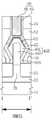
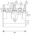
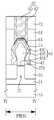
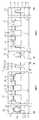
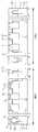
도 1은 본 발명의 기술적 사상의 실시 예에 따른 반도체 소자를 설명하기 위한 단면도 이고, 도 2는 레이아웃 이다. 도 1은 도 2의 절단선 Ⅰ-Ⅰ', Ⅱ-Ⅱ', Ⅲ-Ⅲ', Ⅳ-Ⅳ', Ⅴ-Ⅴ', 및 Ⅵ-Ⅵ' 에 따라 취해진 단면도이다.1 is a cross-sectional view for explaining a semiconductor device according to an embodiment of the inventive concept, and FIG. 2 is a layout. 1 is a cross-sectional view taken along the cutting lines I-I', II-II', III-III', IV-IV', V-V', and VI-VI' of FIG.
도1을 참조하면, 본 발명의 기술적 사상의 실시 예에 따른 반도체 소자는 엔모스(NMOS)영역 및 피모스(PMOS)영역을 갖는 반도체 기판(13) 상에 형성된 N-웰(21), P-웰(22), 소자 분리 막(25), N-형 핀(27), P-형 핀(28), 제1 내측 스페이서(37), 제2 내측 스페이서(38), 제1 하부 스페이서(37A), 제2 하부 스페이서(38A), 제1 소스/드레인(43), 제2 소스/드레인(44), 버퍼 막(45), 제1 외측 스페이서(47), 제2 외측 스페이서(48), 제1 하부 절연 막(51), 제2 하부 절연 막(52), 제1 하부 게이트 유전막(61), 제2 하부 게이트 유전막(62), 제1 상부 게이트 유전막(63), 제2 상부 게이트 유전막(64), 제1 하부 게이트 전극(65), 제2 하부 게이트 전극(66), 제1 상부 게이트 전극(67), 제2 상부 게이트 전극(68), 제1 게이트 전극(69), 제2 게이트 전극(70), 제1 게이트 캐핑 막(71), 제2 게이트 캐핑 막(72), 제1 상부 절연 막(73), 제2 상부 절연 막(74), 제1 플러그 이온 주입 영역(75), 제1 금속 실리사이드 막(81), 제2 금속 실리사이드 막(82), 제1 하부 도전 막(83), 제2 하부 도전 막(84), 제1 상부 도전 막(85), 제2 상부 도전 막(86), 제1 플러그(87), 및 제2 플러그(88)를 포함할 수 있다.Referring to FIG. 1 , in a semiconductor device according to an embodiment of the inventive concept, an N-well 21 , P formed on a semiconductor substrate 13 having an NMOS region and a PMOS region - Well 22, device isolation film 25, N-type fin 27, P-type fin 28, first inner spacer 37, second inner spacer 38, first lower spacer ( 37A), second lower spacer 38A, first source/drain 43 , second source/drain 44 , buffer film 45 , first outer spacer 47 , second outer spacer 48 ) , first lower insulating film 51 , second lower insulating film 52 , first lower gate dielectric film 61 , second lower gate dielectric film 62 , first upper gate dielectric film 63 , second upper gate The dielectric layer 64 , the first lower gate electrode 65 , the second lower gate electrode 66 , the first upper gate electrode 67 , the second upper gate electrode 68 , the first gate electrode 69 , the first 2 gate electrode 70 , first gate capping film 71 , second gate capping film 72 , first upper insulating film 73 , second upper insulating film 74 , first plug ion implantation region ( 75), first metal silicide film 81, second metal silicide film 82, first lower conductive film 83, second lower conductive film 84, first upper conductive film 85, second It may include an upper conductive layer 86 , a first plug 87 , and a second plug 88 .
상기 제1 소스/드레인(43)은 P-형 불순물들을 포함할 수 있으며, 상기 제2 소스/드레인(44)은 N-형 불순물들을 포함할 수 있다. 상기 제1 플러그(87)는 상기 제1 금속 실리사이드 막(81) 및 상기 제1 플러그 이온 주입 영역(75)을 경유하여 상기 제1 소스/드레인(43)에 전기적으로 접속될 수 있다. 상기 제2 플러그(88)는 상기 버퍼 막(45)을 관통하고 상기 제2 금속 실리사이드 막(82)을 경유하여 상기 제2 소스/드레인(44)에 접속될 수 있다. 상기 제1 플러그 이온 주입 영역(75)을 형성하는 동안 상기 버퍼 막(45)은 상기 P-형 불순물들이 상기 제2 소스/드레인(44) 내부로 주입되는 것을 방지하는 역할을 수행할 수 있다. 상기 제1 플러그(87) 및 상기 제1 소스/드레인(43) 사이의 콘택 저항과 상기 제2 플러그(88) 및 상기 제2 소스/드레인(44) 사이의 콘택 저항은 현저히 감소될 수 있다.The first source/
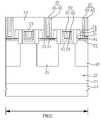
도 2를 참조하면, 상기 반도체 기판(13)의 상기 피모스(PMOS)영역 상에 상기 N-웰(21)이 형성될 수 있다. 상기 N-웰(21) 상에 서로 평행한 다수의 N-형 핀들(27)이 형성될 수 있다. 상기 N-형 핀들(27) 상을 가로지르고 서로 평행한 다수의 제1 게이트 전극들(69)이 형성될 수 있다. 상기 제1 게이트 전극들(69) 사이의 상기 N-형 핀들(27) 상에 다수의 제1 플러그들(87)이 형성될 수 있다.Referring to FIG. 2 , the N-well 21 may be formed on the PMOS region of the
상기 반도체 기판(13)의 상기 엔모스(NMOS)영역 상에 상기 P-웰(22)이 형성될 수 있다. 상기 P-웰(22) 상에 서로 평행한 다수의 P-형 핀들(28)이 형성될 수 있다. 상기 P-형 핀들(28) 상을 가로지르고 서로 평행한 다수의 제2 게이트 전극들(70)이 형성될 수 있다. 상기 제2 게이트 전극들(70) 사이의 상기 P-형 핀들(28) 상에 다수의 제2 플러그들(88)이 형성될 수 있다.The P-well 22 may be formed on the NMOS region of the
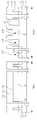
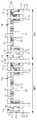
도 3 내지 도 16은 본 발명의 기술적 사상의 실시 예에 따른 반도체 소자를 설명하기 위한 단면도들 이다.3 to 16 are cross-sectional views for explaining a semiconductor device according to an embodiment of the inventive concept.
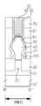
도 3을 참조하면, 제2 소스/드레인(44) 상에 버퍼 막(45)이 형성될 수 있다. 상기 버퍼 막(45) 상에 제2 하부 절연 막(52)이 형성될 수 있다. 상기 제2 하부 절연 막(52) 상에 제2 상부 절연 막(74)이 형성될 수 있다. 상기 제2 상부 절연 막(74) 및 상기 제2 하부 절연 막(52)을 관통하여 상기 제2 소스/드레인(44)에 접속된 제2 플러그(88)가 형성될 수 있다. 상기 제2 플러그(88) 및 상기 제2 소스/드레인(44) 사이에 제2 금속 실리사이드 막(82)이 형성될 수 있다. 상기 제2 하부 절연 막(52) 및 상기 제2 소스/드레인(44) 사이에 언더 컷 영역(52UC)이 형성될 수 있다. 상기 제2 플러그(88)는 상기 언더 컷 영역(52UC) 내에 신장될 수 있다. 상기 제2 플러그(88)는 하단의 수평 폭이 중심의 수평 폭보다 클 수 있다.Referring to FIG. 3 , a
상기 제2 소스/드레인(44)은 결정 성장된 물질을 포함할 수 있다. 상기 제2 소스/드레인(44)은 하부의 수평 폭보다 중간 영역의 수평 폭이 클 수 있다. 상기 제2 소스/드레인(44)의 하단과 중간 영역 사이의 측면은 역-경사를 보일 수 있다. 상기 버퍼 막(45)은 결정 성장된 물질을 포함할 수 있다. 상기 버퍼 막(45)은 상기 제2 소스/드레인(44) 상에 한정될 수 있다. 상기 버퍼 막(45)은 상기 제2 소스/드레인(44)에 스트레스를 주지 않는 임계 두께(critical thickness)보다 두꺼울 수 있다. 예를 들면, 상기 버퍼 막(45)의 두께는 3 nm 이상으로 형성될 수 있다. 상기 버퍼 막(45)은 상기 제2 소스/드레인(44)의 역-경사진 측면에 접촉될 수 있다. 상기 버퍼 막(45)의 하단과 중간 영역 사이의 측면은 역-경사를 보일 수 있다.The second source/
도 4를 참조하면, 제2 플러그(88)의 수평 폭은 상기 제2 소스/드레인(44)보다 클 수 있다.Referring to FIG. 4 , the horizontal width of the
도 5를 참조하면, 제2 소스/드레인(44)은 제2 하부 반도체 막(44L) 및 제2 상부 반도체 막(44U)을 포함할 수 있다. 예를 들면, 상기 제2 하부 반도체 막(44L)은 에스이지(selective epitaxial growth; SEG) 방법을 이용하여 형성된 SiC막을 포함할 수 있다. 상기 제2 상부 반도체 막(44U)은 에스이지(selective epitaxial growth; SEG) 방법을 이용하여 형성된 Si막을 포함할 수 있다.Referring to FIG. 5 , the second source/
도 6을 참조하면, 제2 소스/드레인(44E)은 제2 하부 반도체 패턴(44D) 및 제2 상부 반도체 막(44C)을 포함할 수 있다. 상기 제2 하부 반도체 패턴(44D)은 P-형 핀(28) 내에 N-형 불순물들을 주입하여 형성될 수 있다. 상기 제2 상부 반도체 막(44C)은 상기 제2 하부 반도체 패턴(44D) 상에 에스이지(selective epitaxial growth; SEG) 방법을 이용하여 형성된 Si 막을 포함할 수 있다.Referring to FIG. 6 , the second source/
도 7을 참조하면, 제2 하부 절연 막(52)의 하부에 언더 컷 영역(52UC)이 형성될 수 있다. 제2 외측 스페이서(48) 및 제2 소스/드레인(44) 사이에 버퍼 막(45)이 보존될 수 있다. 제2 플러그(88)는 상기 언더 컷 영역(52UC) 내에 신장될 수 있다. 상기 제2 플러그(88)는 하단의 수평 폭이 중심의 수평 폭보다 클 수 있다. 제2 금속 실리사이드 막(82)은 P-형 핀(28)의 상단보다 높은 레벨에 형성될 수 있다.Referring to FIG. 7 , an undercut region 52UC may be formed under the second lower insulating
도 8을 참조하면, 제2 플러그(88)는 제2 외측 스페이서(48) 및 제2 소스/드레인(44) 사이에 신장될 수 있다. 상기 제2 플러그(88)는 제2 내측 스페이서(38)의 측면에 직접적으로 접촉될 수 있다.Referring to FIG. 8 , the
도 9를 참조하면, 제2 소스/드레인(44)은 제2 하부 반도체 막(44L) 및 제2 상부 반도체 막(44U)을 포함할 수 있다. 제2 금속 실리사이드 막(82)은 상기 제2 상부 반도체 막(44U) 상에 형성될 수 있다.Referring to FIG. 9 , the second source/
도 10을 참조하면, 제2 소스/드레인(44E)은 제2 하부 반도체 패턴(44D) 및 제2 상부 반도체 막(44C)을 포함할 수 있다. 제2 금속 실리사이드 막(82)은 상기 제2 상부 반도체 막(44C) 상에 형성될 수 있다.Referring to FIG. 10 , the second source/
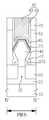
도 11을 참조하면, 제1 소스/드레인(43) 상에 제1 하부 절연 막(51)이 형성될 수 있다. 상기 제1 하부 절연 막(51) 상에 제1 상부 절연 막(73)이 형성될 수 있다. 상기 제1 상부 절연 막(73) 및 상기 제1 하부 절연 막(51)을 관통하여 상기 제1 소스/드레인(43)에 접속된 제1 플러그(87)가 형성될 수 있다. 상기 제1 플러그(87) 및 상기 제1 소스/드레인(43) 사이에 제1 플러그 이온 주입 영역(75)이 형성될 수 있다. 상기 제1 플러그 이온 주입 영역(75) 내에 제1 금속 실리사이드 막(81)이 형성될 수 있다. 상기 제1 금속 실리사이드 막(81)은 상기 제1 플러그(87) 및 상기 제1 플러그 이온 주입 영역(75) 사이에 형성될 수 있다. 상기 제1 플러그 이온 주입 영역(75)의 P-형 불순물 농도는 상기 제1 소스/드레인(43) 보다 높을 수 있다.Referring to FIG. 11 , a first lower insulating
도 12를 참조하면, 제1 플러그(87)의 수평 폭은 상기 제1 소스/드레인(43)보다 클 수 있다.Referring to FIG. 12 , the horizontal width of the
도 13을 참조하면, 제1 소스/드레인(43)은 제1 하부 반도체 막(43A), 제1 중간 반도체 막(43B), 및 제1 상부 반도체 막(43C)을 포함할 수 있다. 상기 제1 상부 반도체 막(43C) 내에 제1 플러그 이온 주입 영역(75)이 형성될 수 있다. 상기 제1 플러그 이온 주입 영역(75) 상에 제1 금속 실리사이드 막(81)이 형성될 수 있다.Referring to FIG. 13 , the first source/
상기 제1 하부 반도체 막(43A)은 에스이지(selective epitaxial growth; SEG) 방법에 의한 언도프드(undoped) 단결정 SiGe를 포함할 수 있다. 상기 제1 하부 반도체 막(43A) 상에 상기 제1 중간 반도체 막(43B)이 형성될 수 있다. 상기 제1 중간 반도체 막(43B)은 에스이지(selective epitaxial growth; SEG) 방법에 의한 보론(B) 도프드(doped) 단결정 SiGe를 포함할 수 있다. 상기 제1 중간 반도체 막(43B) 상에 상기 제1 상부 반도체 막(43C)이 형성될 수 있다. 상기 제1 상부 반도체 막(43C)은 에스이지(selective epitaxial growth; SEG) 방법에 의한 보론(B) 도프드(doped) 단결정 Si을 포함할 수 있다.The first
도 14를 참조하면, 제1 플러그 이온 주입 영역(75) 내에 제1 금속 실리사이드 막(81)이 형성될 수 있다. 상기 제1 금속 실리사이드 막(81)은 제1 플러그(87) 및 상기 제1 플러그 이온 주입 영역(75) 사이에 형성될 수 있다. 상기 제1 플러그 이온 주입 영역(75)의 P-형 불순물 농도는 제1 소스/드레인(43) 보다 높을 수 있다. 상기 제1 금속 실리사이드 막(81)은 N-형 핀(27)의 상단보다 높은 레벨에 형성될 수 있다.Referring to FIG. 14 , a first
도 15를 참조하면, 제1 금속 실리사이드 막(81)은 제1 외측 스페이서(47)의 하부에 신장될 수 있다. 상기 제1 금속 실리사이드 막(81)은 제1 내측 스페이서(37)의 측면에 직접적으로 접촉될 수 있다.Referring to FIG. 15 , the first
도 16을 참조하면, 제1 소스/드레인(43)은 제1 하부 반도체 막(43A), 제1 중간 반도체 막(43B), 및 제1 상부 반도체 막(43C)을 포함할 수 있다. 상기 제1 상부 반도체 막(43C) 내에 제1 플러그 이온 주입 영역(75)이 형성될 수 있다. 상기 제1 플러그 이온 주입 영역(75) 상에 제1 금속 실리사이드 막(81)이 형성될 수 있다.Referring to FIG. 16 , the first source/
예를 들면, 상기 제1 하부 반도체 막(43A)은 에스이지(selective epitaxial growth; SEG) 방법에 의한 언도프드(undoped) 단결정 SiGe를 포함할 수 있다. 상기 제1 하부 반도체 막(43A) 내에서 Ge의 함량은 10-25% 일 수 있다. 상기 제1 하부 반도체 막(43A) 상에 상기 제1 중간 반도체 막(43B)이 형성될 수 있다. 상기 제1 중간 반도체 막(43B)의 상단은 N-형 핀(27)의 상단보다 높은 레벨에 돌출될 수 있다. 상기 제1 중간 반도체 막(43B)은 에스이지(selective epitaxial growth; SEG) 방법에 의한 보론(B) 도프드(doped) 단결정 SiGe를 포함할 수 있다. 상기 제1 중간 반도체 막(43B) 내에서 Ge의 함량은 25-50% 일 수 있다. 상기 제1 중간 반도체 막(43B) 상에 상기 제1 상부 반도체 막(43C)이 형성될 수 있다. 상기 제1 상부 반도체 막(43C)은 에스이지(selective epitaxial growth; SEG) 방법에 의한 보론(B) 도프드(doped) 단결정 Si을 포함할 수 있다.For example, the first
도 17 내지 도 22는 본 발명의 기술적 사상의 실시 예에 따른 반도체 소자를 설명하기 위한 단면도들 이다.17 to 22 are cross-sectional views for explaining a semiconductor device according to an embodiment of the inventive concept.
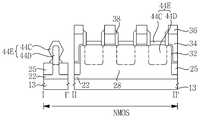
도 17을 참조하면, 반도체 기판(13)의 엔모스(NMOS)영역 상에 P-웰(22)이 형성될 수 있다. 상기 P-웰(22) 상에 서로 평행한 다수의 P-형 핀들(28)이 형성될 수 있다. 상기 P-형 핀들(28) 상에 제2 소스/드레인들(44)이 형성될 수 있다. 상기 제2 소스/드레인들(44) 상에 버퍼 막들(45)이 형성될 수 있다. 상기 버퍼 막들(45) 상에 제2 하부 절연 막(52)이 형성될 수 있다. 상기 제2 하부 절연 막(52) 상에 제2 상부 절연 막(74)이 형성될 수 있다. 상기 제2 상부 절연 막(74) 및 상기 제2 하부 절연 막(52)을 관통하여 상기 제2 소스/드레인들(44)에 접속된 제2 플러그(88)가 형성될 수 있다. 상기 제2 플러그(88) 및 상기 제2 소스/드레인들(44) 사이에 제2 금속 실리사이드 막들(82)이 형성될 수 있다.Referring to FIG. 17 , a P-well 22 may be formed on an NMOS region of the
도 18을 참조하면, 반도체 기판(13)의 피모스(PMOS)영역 상에 N-웰(21)이 형성될 수 있다. 상기 N-웰(21) 상에 서로 평행한 다수의 N-형 핀들(27)이 형성될 수 있다. 상기 N-형 핀들(27) 상에 제1 소스/드레인들(43)이 형성될 수 있다. 상기 제1 소스/드레인들(43) 상에 제1 하부 절연 막(51)이 형성될 수 있다. 상기 제1 하부 절연 막(51) 상에 제1 상부 절연 막(73)이 형성될 수 있다. 상기 제1 상부 절연 막(73) 및 상기 제1 하부 절연 막(51)을 관통하여 상기 제1 소스/드레인들(43)에 접속된 제1 플러그(87)가 형성될 수 있다. 상기 제1 플러그(87) 및 상기 제1 소스/드레인들(43) 사이에 제1 플러그 이온 주입 영역들(75)이 형성될 수 있다. 상기 제1 플러그 이온 주입 영역들(75) 내에 제1 금속 실리사이드 막들(81)이 형성될 수 있다.Referring to FIG. 18 , an N-well 21 may be formed on a PMOS region of the
도 19를 참조하면, 버퍼 막들(45)은 서로 접촉될 수 있다.Referring to FIG. 19 , the buffer layers 45 may be in contact with each other.
도 20을 참조하면, 제1 금속 실리사이드 막들(81)은 서로 접촉될 수 있다.Referring to FIG. 20 , the first metal silicide layers 81 may contact each other.
도 21을 참조하면, 제2 소스/드레인들(44)은 서로 접촉될 수 있다. 제2 금속 실리사이드 막들(82)은 서로 접촉될 수 있다.Referring to FIG. 21 , the second sources/drains 44 may be in contact with each other. The second metal silicide layers 82 may contact each other.
도 22를 참조하면, 제1 소스/드레인들(43)은 서로 접촉될 수 있다. 제1 플러그 이온 주입 영역들(75)은 서로 접촉될 수 있다. 제1 금속 실리사이드 막들(81)은 서로 접촉될 수 있다.Referring to FIG. 22 , the first sources/drains 43 may be in contact with each other. The first plug
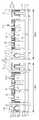
도 23 내지 도 49는 본 발명의 기술적 사상의 실시 예에 따른 반도체 소자의 형성 방법을 설명하기 위하여 도 2의 절단선 Ⅰ-Ⅰ', Ⅱ-Ⅱ', Ⅲ-Ⅲ', Ⅳ-Ⅳ', Ⅴ-Ⅴ', 및 Ⅵ-Ⅵ'에 따라 취해진 단면도들 이다.23 to 49 are cut-off lines I-I', II-II', III-III', IV-IV', Cross-sectional views taken according to Ⅴ-Ⅴ', and Ⅵ-Ⅵ'.
도 2 및 도 23을 참조하면, 엔모스(NMOS)영역 및 피모스(PMOS)영역을 갖는 반도체 기판(13) 상에 N-웰(21), P-웰(22), 소자 분리 막(25), N-형 핀(27), 및 P-형 핀(28)이 형성될 수 있다.2 and 23 , the N-well 21 , the P-well 22 , and the
상기 반도체 기판(13)은 벌크 웨이퍼 또는 에스오아이(silicon on insulator; SOI)웨이퍼일 수 있다. 예를 들면, 상기 반도체 기판(13)은 P-형 불순물들을 갖는 단결정 실리콘 웨이퍼일 수 있다. 상기 N-웰(21)은 상기 피모스(PMOS)영역 상에 형성될 수 있다. 상기 N-웰(21)은 N-형 불순물들을 포함할 수 있다. 예를 들면, 상기 N-형 불순물들은 P, As, 또는 이들의 조합을 포함할 수 있다. 상기 N-형 핀(27)은 상기 소자 분리 막(25)에 의하여 상기 N-웰(21) 상에 한정될 수 있다. 상기 N-형 핀(27)은 N-형 불순물들을 포함할 수 있다. 예를 들면, 상기 N-형 핀(27)은 상기 N-형 불순물들을 갖는 단결정 실리콘을 포함할 수 있다. 상기 N-형 핀(27)은 폭보다 높이가 클 수 있다. 상기 N-형 핀(27)의 상단은 상기 소자 분리 막(25)보다 높은 레벨에 돌출될 수 있다. 상기 N-형 핀(27)의 측면들은 노출될 수 있다. 상기 N-형 핀(27)의 상부 모서리들은 둥글게 형성될 수 있다.The
상기 P-웰(22)은 상기 엔모스(NMOS)영역 상에 형성될 수 있다. 상기 P-웰(22)은 P-형 불순물들을 포함할 수 있다. 예를 들면, 상기 P-형 불순물들은 B, BF, BF2, 또는 이들의 조합을 포함할 수 있다. 상기 P-형 핀(28)은 상기 소자 분리 막(25)에 의하여 상기 P-웰(22) 상에 한정될 수 있다. 상기 P-형 핀(28)은 상기 P-형 불순물들을 포함할 수 있다. 예를 들면, 상기 P-형 핀(28)은 상기 P-형 불순물들을 갖는 단결정 실리콘을 포함할 수 있다. 상기 P-형 핀(28)은 폭보다 높이가 클 수 있다. 상기 P-형 핀(28)의 상단은 상기 소자 분리 막(25)보다 높은 레벨에 돌출될 수 있다. 상기 P-형 핀(28)의 측면들은 노출될 수 있다. 다른 실시 예에서, 상기 P-웰(22)은 생략될 수 있다. 상기 P-형 핀(28)의 상부 모서리들은 둥글게 형성될 수 있다.The P-well 22 may be formed on the NMOS region. The P-well 22 may include P-type impurities. For example, the P-type impurities may include B, BF, BF2, or a combination thereof. The P-
상기 소자 분리 막(25)은 에스티아이(shallow trench isolation; STI)기술을 이용하여 형성될 수 있다. 상기 소자 분리 막(25)을 형성하는 것은 박막 형성 공정, 화학 기계적 연마(chemical mechanical polishing; CMP) 공정, 에치-백(etch-back)공정, 또는 이들의 조합을 포함할 수 있다. 상기 소자 분리 막(25)은 실리콘 산화물, 실리콘 질화물, 실리콘 산-질화물, 또는 이들의 조합과 같은 절연 막을 포함할 수 있다. 상기 소자 분리 막(25)의 상단은 상기 N-형 핀(27) 및 상기 P-형 핀(28)의 상단들보다 낮은 레벨에 형성될 수 있다. 상기 소자 분리 막(25)은 상기 N-형 핀(27) 및 상기 P-형 핀(28)의 측면들에 접촉될 수 있다.The
도 24를 참조하면, 상기 반도체 기판(13) 상에 가설 버퍼 막(31L), 가설 게이트 막(33L), 및 가설 캐핑 막(35L)이 차례로 형성될 수 있다. 상기 가설 버퍼 막(31L)은 실리콘 산화물을 포함할 수 있다. 상기 가설 게이트 막(33L)은 폴리실리콘을 포함할 수 있다. 상기 가설 캐핑 막(35L)은 실리콘 산화물, 실리콘 질화물, 실리콘 산-질화물, 또는 이들의 조합을 포함할 수 있다.24 , a
상기 피모스(PMOS)영역 상의 상기 가설 버퍼 막(31L), 상기 가설 게이트 막(33L), 및 상기 가설 캐핑 막(35L)을 패터닝하여 제1 가설 버퍼 패턴(31), 제1 가설 게이트 패턴(33), 및 제1 가설 캐핑 패턴(35)이 형성될 수 있다. 상기 제1 가설 게이트 패턴(33)은 상기 N-형 핀(27)의 상부 및 측면들을 덮고 상기 소자 분리 막(25) 상에 연장될 수 있다. 상기 제1 가설 버퍼 패턴(31)은 상기 제1 가설 게이트 패턴(33) 및 상기 N-형 핀(27) 사이에 보존될 수 있다.The
상기 가설 버퍼 막(31L), 상기 가설 게이트 막(33L), 및 상기 가설 캐핑 막(35L)은 상기 엔모스(NMOS)영역 상에 보존될 수 있다.The
도 25를 참조하면, 상기 제1 가설 게이트 패턴(33)의 측면들 상에 제1 내측 스페이서(37)가 형성될 수 있다. 상기 제1 내측 스페이서(37)를 형성하는 동안 상기 N-형 핀(27)의 노출된 측면 상에 제1 하부 스페이서(37A)가 형성될 수 있다.Referring to FIG. 25 , first
상기 제1 내측 스페이서(37)를 형성하는 것은 박막 형성 공정 및 이방성 식각 공정을 포함할 수 있다. 상기 제1 내측 스페이서(37)는 실리콘 산화물, 실리콘 질화물, 실리콘 산-질화물, 또는 이들의 조합과 같은 절연 막을 포함할 수 있다. 예를 들면, 상기 제1 내측 스페이서(37)는 실리콘 질화물을 포함할 수 있다. 상기 제1 가설 게이트 패턴(33) 및 상기 제1 내측 스페이서(37)의 외측에 상기 N-형 핀(27)이 노출될 수 있다.Forming the first
다른 실시 예에서, 상기 제1 하부 스페이서(37A)는 제거될 수 있다.In another embodiment, the first
도 26을 참조하면, 상기 N-형 핀(27)의 노출된 영역을 제거하여 제1 리세스 영역(27R)이 형성될 수 있다. 상기 제1 리세스 영역(27R)의 형성에는 이방성 식각 공정, 등방성 식각 공정, 방향성 식각 공정, 또는 이들의 조합이 적용될 수 있다. 상기 제1 리세스 영역(27R)은 상기 제1 내측 스페이서(37)의 외측에 정렬될 수 있다. 상기 제1 리세스 영역(27R)은 상기 제1 내측 스페이서(37)의 하부에 확장될 수 있다. 상기 제1 리세스 영역(27R)의 바닥은 상기 제1 하부 스페이서(37A)보다 낮은 레벨에 형성될 수 있다. 상기 제1 리세스 영역(27R)의 측벽들 및 바닥에 상기 N-형 핀(27)이 노출될 수 있다. 상기 제1 내측 스페이서(37)의 바닥은 상기 제1 리세스 영역(27R) 내에 노출될 수 있다.Referring to FIG. 26 , a
도 27을 참조하면, 상기 제1 리세스 영역(27R) 내에 제1 소스/드레인(43)이 형성될 수 있다.Referring to FIG. 27 , a first source/
상기 제1 소스/드레인(43)은 결정 성장된 물질을 포함할 수 있다. 상기 제1 소스/드레인(43)은 SiGe, Si, 또는 이들의 조합을 포함할 수 있다. 상기 제1 소스/드레인(43)은 상기 제1 리세스 영역(27R)을 채우고 상기 N-형 핀(27)의 상단보다 높은 레벨에 돌출될 수 있다. 상기 제1 소스/드레인(43)은 상승된 소스/드레인(elevated source/drain)으로 지칭될 수 있다. 상기 제1 소스/드레인(43)은 스트레서(stressor)로 해석될 수 있다. 상기 제1 소스/드레인(43)은 P-형 불순물들을 포함할 수 있다. 상기 제1 소스/드레인(43)은B, BF, 또는 이들의 조합을 포함할 수 있다.The first source/
예를 들면, 상기 제1 소스/드레인(43)은 에스이지(selective epitaxial growth; SEG) 방법을 이용하여 형성된 SiGe막을 포함할 수 있다. 상기 제1 소스/드레인(43)은 하부의 수평 폭보다 중간 영역의 수평 폭이 클 수 있다. 상기 제1 소스/드레인(43)의 하단과 중간 영역 사이의 측면은 역-경사를 보일 수 있다. 상기 제1 소스/드레인(43)의 상단은 상기 제1 내측 스페이서(37)의 하단보다 높은 레벨에 돌출될 수 있다. 상기 제1 소스/드레인(43)의 상단은 상기 제1 하부 스페이서(37A)의 상단보다 높은 레벨에 돌출될 수 있다.For example, the first source/
도 28을 참조하면, 다른 실시 예에서, 제1 소스/드레인(43)은 제1 하부 반도체 막(43A), 제1 중간 반도체 막(43B), 및 제1 상부 반도체 막(43C)을 포함할 수 있다.Referring to FIG. 28 , in another embodiment, the first source/
예를 들면, 상기 제1 하부 반도체 막(43A)은 에스이지(selective epitaxial growth; SEG) 방법에 의한 언도프드(undoped) 단결정 SiGe를 포함할 수 있다. 상기 제1 하부 반도체 막(43A) 내에서 Ge의 함량은 10-25% 일 수 있다. 상기 제1 하부 반도체 막(43A)은 상기 제1 리세스 영역(27R)의 내벽을 컨포말하게 덮을 수 있다.For example, the first
상기 제1 하부 반도체 막(43A) 상에 상기 제1 중간 반도체 막(43B)이 형성될 수 있다. 상기 제1 중간 반도체 막(43B)은 상기 제1 리세스 영역(27R)을 완전히 채울 수 있다. 상기 제1 중간 반도체 막(43B)의 상단은 상기 N-형 핀(27)의 상단보다 높은 레벨에 돌출될 수 있다. 상기 제1 중간 반도체 막(43B)은 에스이지(selective epitaxial growth; SEG) 방법에 의한 보론(B) 도프드(doped) 단결정 SiGe를 포함할 수 있다. 상기 제1 중간 반도체 막(43B) 내에서 Ge의 함량은 25-50% 일 수 있다. 상기 제1 중간 반도체 막(43B)은 1E20-3E20 atom/㎤ 의 보론(B)을 함유할 수 있다.The first
상기 제1 중간 반도체 막(43B) 상에 상기 제1 상부 반도체 막(43C)이 형성될 수 있다. 상기 제1 상부 반도체 막(43C)은 에스이지(selective epitaxial growth; SEG) 방법에 의한 보론(B) 도프드(doped) 단결정 Si을 포함할 수 있다. 상기 제1 상부 반도체 막(43C)은 1E20-3E20 atom/㎤ 의 보론(B)을 함유할 수 있다.The first
다른 실시 예에서, 상기 제1 하부 반도체 막(43A) 또는 상기 제1 상부 반도체 막(43C)은 생략될 수 있다.In another embodiment, the first
도 29를 참조하면, 상기 제1 내측 스페이서(37)의 측면에 제1 외측 스페이서(47)가 형성될 수 있다. 상기 제1 외측 스페이서(47)는 상기 제1 하부 스페이서(37A)를 덮고 상기 제1 소스/드레인(43)의 측면을 부분적으로 덮을 수 있다. 상기 제1 소스/드레인(43)의 하단과 중간 영역 사이의 측면은 역-경사를 보일 수 있다. 상기 제1 소스/드레인(43)의 역-경사진 측면은 상기 제1 외측 스페이서(47)로 덮일 수 있다. 상기 제1 외측 스페이서(47)의 바닥은 상기 제1 소스/드레인(43)의 상부 표면에 접촉될 수 있다.Referring to FIG. 29 , a first
상기 제1 외측 스페이서(47)를 형성하는 것은 박막 형성 공정 및 이방성 식각 공정을 포함할 수 있다. 상기 제1 외측 스페이서(47)는 실리콘 산화물, 실리콘 질화물, 실리콘 산-질화물, 또는 이들의 조합과 같은 절연 막을 포함할 수 있다. 예를 들면, 상기 제1 외측 스페이서(47)는 실리콘 질화물을 포함할 수 있다.Forming the first
도 30을 참조하면, 상기 제1 소스/드레인(43) 상에 제1 하부 절연 막(51)이 형성될 수 있다. 상기 반도체 기판(13)의 전면을 덮는 식각 정지 막(53)이 형성될 수 있다.Referring to FIG. 30 , a first lower insulating
상기 제1 하부 절연 막(51)을 형성하는 것은 박막 형성 공정 및 평탄화 공정을 포함할 수 있다. 상기 평탄화 공정은 화학 기계적 연마(chemical mechanical polishing; CMP) 공정, 에치-백(etch-back)공정, 또는 이들의 조합을 포함할 수 있다. 상기 제1 하부 절연 막(51)은 실리콘 산화물, 실리콘 질화물, 실리콘 산-질화물, 또는 이들의 조합과 같은 절연 막을 포함할 수 있다. 예를 들면, 상기 제1 하부 절연 막(51)은 실리콘 산화물을 포함할 수 있다.Forming the first lower insulating
상기 식각 정지 막(53)은 실리콘 산화물, 실리콘 질화물, 실리콘 산-질화물, 또는 이들의 조합과 같은 절연 막을 포함할 수 있다. 다른 실시 예에서, 상기 식각 정지 막(53)은 생략될 수 있다.The
도 31을 참조하면, 상기 엔모스(NMOS)영역 상의 상기 식각 정지 막(53)을 제거하여 상기 가설 캐핑 막(35L)이 노출될 수 있다. 상기 식각 정지 막(53)은 상기 피모스(PMOS)영역 상에 보존될 수 있다.Referring to FIG. 31 , the
도 32를 참조하면, 상기 엔모스(NMOS)영역 상의 상기 가설 버퍼 막(31L), 상기 가설 게이트 막(33L), 및 상기 가설 캐핑 막(35L)을 패터닝하여 제2 가설 버퍼 패턴(32), 제2 가설 게이트 패턴(34), 및 제2 가설 캐핑 패턴(36)이 형성될 수 있다. 상기 제2 가설 게이트 패턴(34)은 상기 P-형 핀(28)의 상부 및 측면들을 덮고 상기 소자 분리 막(25) 상에 연장될 수 있다. 상기 제2 가설 버퍼 패턴(32)은 상기 제2 가설 게이트 패턴(34) 및 상기 P-형 핀(28) 사이에 보존될 수 있다.32, a second
상기 제2 가설 게이트 패턴(34)의 측면들 상에 제2 내측 스페이서(38)가 형성될 수 있다. 상기 제2 내측 스페이서(38)를 형성하는 동안 상기 P-형 핀(28)의 노출된 측면 상에 제2 하부 스페이서(38A)가 형성될 수 있다.Second
상기 제2 내측 스페이서(38)를 형성하는 것은 박막 형성 공정 및 이방성 식각 공정을 포함할 수 있다. 상기 제2 내측 스페이서(38)는 실리콘 산화물, 실리콘 질화물, 실리콘 산-질화물, 또는 이들의 조합과 같은 절연 막을 포함할 수 있다. 예를 들면, 상기 제2 내측 스페이서(38)는 실리콘 질화물을 포함할 수 있다. 상기 제2 가설 게이트 패턴(34) 및 상기 제2 내측 스페이서(38)의 외측에 상기 P-형 핀(28)이 노출될 수 있다.Forming the second
다른 실시 예에서, 상기 제2 하부 스페이서(38A)는 제거될 수 있다.In another embodiment, the second
도 33을 참조하면, 상기 P-형 핀(28)의 노출된 영역을 제거하여 제2 리세스 영역(28R)이 형성될 수 있다.Referring to FIG. 33 , a
상기 제2 리세스 영역(28R)의 형성에는 이방성 식각 공정, 등방성 식각 공정, 방향성 식각 공정, 또는 이들의 조합이 적용될 수 있다. 상기 제2 리세스 영역(28R)은 상기 제2 내측 스페이서(38)의 외측에 정렬될 수 있다. 상기 제2 리세스 영역(28R)은 상기 제2 내측 스페이서(38)의 하부에 확장될 수 있다. 상기 제2 리세스 영역(28R)의 바닥은 상기 제2 하부 스페이서(38A)보다 낮은 레벨에 형성될 수 있다. 상기 제2 리세스 영역(28R)의 측벽들 및 바닥에 상기 P-형 핀(28)이 노출될 수 있다. 상기 제2 내측 스페이서(38)의 바닥은 상기 제2 리세스 영역(28R) 내에 노출될 수 있다.An anisotropic etching process, an isotropic etching process, a directional etching process, or a combination thereof may be applied to the formation of the
도 34를 참조하면, 상기 제2 리세스 영역(28R) 내에 제2 소스/드레인(44)이 형성될 수 있다.Referring to FIG. 34 , a second source/
상기 제2 소스/드레인(44)은 결정 성장된 물질을 포함할 수 있다. 상기 제2 소스/드레인(44)은 SiC, Si, 또는 이들의 조합을 포함할 수 있다. 상기 제2 소스/드레인(44)은 상기 제2 리세스 영역(28R)을 채우고 상기 P-형 핀(28)의 상단보다 높은 레벨에 돌출될 수 있다. 상기 제2 소스/드레인(44)은 상승된 소스/드레인(elevated source/drain)으로 지칭될 수 있다. 상기 제2 소스/드레인(44)은 스트레서(stressor)로 해석될 수 있다. 상기 제2 소스/드레인(44)은 N-형 불순물들을 포함할 수 있다. 상기 제2 소스/드레인(44)은 P, As, 또는 이들의 조합을 포함할 수 있다.The second source/
예를 들면, 상기 제2 소스/드레인(44)은 에스이지(selective epitaxial growth; SEG) 방법을 이용하여 형성된 SiC막을 포함할 수 있다. 상기 제2 소스/드레인(44)은 하부의 수평 폭보다 중간 영역의 수평 폭이 클 수 있다. 상기 제2 소스/드레인(44)의 하단과 중간 영역 사이의 측면은 역-경사를 보일 수 있다. 상기 제2 소스/드레인(44)의 상단은 상기 제2 내측 스페이서(38)의 하단보다 높은 레벨에 돌출될 수 있다. 상기 제2 소스/드레인(44)의 상단은 상기 제2 하부 스페이서(38A)의 상단보다 높은 레벨에 돌출될 수 있다.For example, the second source/
도 35를 참조하면, 다른 실시 예에서, 제2 소스/드레인(44E)은 제2 하부 반도체 패턴(44D) 및 제2 상부 반도체 막(44C)을 포함할 수 있다.Referring to FIG. 35 , in another embodiment, the second source/
상기 제2 하부 반도체 패턴(44D)은 상기 P-형 핀(28) 내에 N-형 불순물들을 주입하여 형성될 수 있다. 상기 제2 상부 반도체 막(44C)은 상기 제2 하부 반도체 패턴(44D) 상에 에스이지(selective epitaxial growth; SEG) 방법을 이용하여 형성될 수 있다. 상기 제2 상부 반도체 막(44C)은 Si 막을 포함할 수 있다. 상기 제2 상부 반도체 막(44C)은 N-형 불순물들을 포함할 수 있다.The second
도 36을 참조하면, 상기 제2 소스/드레인(44) 상에 버퍼 막(45)이 형성될 수 있다. 상기 버퍼 막(45)은 상기 제2 소스/드레인(44) 상에 한정될 수 있다. 상기 버퍼 막(45)은 상기 제2 소스/드레인(44) 상에 자기-정렬될(self-aligned) 수 있다. 상기 버퍼 막(45)은 상기 제2 소스/드레인(44)의 상부 표면 및 측면들에 직접적으로 접촉될 수 있다. 상기 버퍼 막(45)은 상기 제2 내측 스페이서(38)의 측면에 직접적으로 접촉될 수 있다.Referring to FIG. 36 , a
상기 버퍼 막(45)은 결정 성장된 물질을 포함할 수 있다. 상기 버퍼 막(45)은 상기 제1 소스/드레인(43)의 표면을 구성하는 물질에 대하여 식각 선택비를 갖는 물질을 포함할 수 있다. 상기 버퍼 막(45)은 상기 제2 소스/드레인(44)의 표면을 구성하는 물질에 대하여 식각 선택비를 갖는 물질을 포함할 수 있다. 상기 버퍼 막(45)은 상기 제1 소스/드레인(43) 및 상기 제2 소스/드레인(44)의 표면을 구성하는 물질과 다른 물질을 포함할 수 있다. 상기 버퍼 막(45)은 에스이지(selective epitaxial growth; SEG) 방법을 이용하여 상기 제2 소스/드레인(44)의 표면을 따라 형성될 수 있다. 예를 들면, 상기 버퍼 막(45)은 Ge막, 또는 SiGe 막을 포함할 수 있다. 상기 버퍼 막(45)은 상기 제2 소스/드레인(44)에 스트레스를 주지 않는 임계 두께(critical thickness)보다 두꺼울 수 있다. 예를 들면, 상기 버퍼 막(45)의 두께는 3 nm 이상으로 형성될 수 있다. 상기 버퍼 막(45)의 두께는 3 nm 20 nm 일 수 있다.The
도 37을 참조하면, 상기 제2 내측 스페이서(38)의 측면에 제2 외측 스페이서(48)가 형성될 수 있다. 상기 제2 외측 스페이서(48)는 상기 제2 하부 스페이서(38A)를 덮고 상기 버퍼 막(45)의 측면을 부분적으로 덮을 수 있다.Referring to FIG. 37 , a second
상기 버퍼 막(45)의 하단과 중간 영역 사이의 측면은 역-경사를 보일 수 있다. 상기 버퍼 막(45)의 역-경사진 측면은 상기 제2 외측 스페이서(48)로 덮일 수 있다. 상기 제2 외측 스페이서(48)의 바닥은 상기 버퍼 막(45)의 상부 표면에 접촉될 수 있다.A side surface between the lower end and the middle region of the
상기 제2 외측 스페이서(48)를 형성하는 것은 박막 형성 공정 및 이방성 식각 공정을 포함할 수 있다. 상기 제2 외측 스페이서(48)는 실리콘 산화물, 실리콘 질화물, 실리콘 산-질화물, 또는 이들의 조합과 같은 절연 막을 포함할 수 있다. 예를 들면, 상기 제2 외측 스페이서(48)는 실리콘 질화물을 포함할 수 있다. 상기 제2 외측 스페이서(48)의 외측에 상기 버퍼 막(45)의 상부 표면이 노출될 수 있다.Forming the second
도 38을 참조하면, 상기 버퍼 막(45) 상에 제2 하부 절연 막(52)이 형성될 수 있다. 상기 제2 하부 절연 막(52)을 형성하는 것은 박막 형성 공정 및 평탄화 공정을 포함할 수 있다. 상기 평탄화 공정은 화학 기계적 연마(chemical mechanical polishing; CMP) 공정, 에치-백(etch-back)공정, 또는 이들의 조합을 포함할 수 있다. 상기 제2 하부 절연 막(52)은 실리콘 산화물, 실리콘 질화물, 실리콘 산-질화물, 또는 이들의 조합과 같은 절연 막을 포함할 수 있다. 예를 들면, 상기 제2 하부 절연 막(52)은 실리콘 산화물을 포함할 수 있다.Referring to FIG. 38 , a second lower insulating
도 39를 참조하면, 화학 기계적 연마(chemical mechanical polishing; CMP) 공정을 이용하여 상기 제1 가설 게이트 패턴(33) 및 상기 제2 가설 게이트 패턴(34)이 노출될 수 있다. 상기 식각 정지 막(53), 상기 제1 가설 캐핑 패턴(35), 및 상기 제2 가설 캐핑 패턴(36)은 제거될 수 있다.Referring to FIG. 39 , the first
도 40을 참조하면, 상기 제1 가설 게이트 패턴(33), 상기 제2 가설 게이트 패턴(34), 상기 제1 가설 버퍼 패턴(31), 및 상기 제2 가설 버퍼 패턴(32)을 제거하여 제1 게이트 트렌치(33T) 및 제2 게이트 트렌치(34T)가 형성될 수 있다. 상기 제1 게이트 트렌치(33T) 내에 상기 N-형 핀(27)의 상부표면 및 측면들이 노출될 수 있다. 상기 제2 게이트 트렌치(34T) 내에 상기 P-형 핀(28)의 상부표면 및 측면들이 노출될 수 있다.Referring to FIG. 40 , the first
도 41을 참조하면, 제1 하부 게이트 유전막(61) 및 제2 하부 게이트 유전막(62)이 형성될 수 있다. 상기 제1 하부 게이트 유전막(61)은 상기 N-형 핀(27)의 상부표면 및 측면들 상에 형성될 수 있다. 상기 제1 하부 게이트 유전막(61)은 상기 N-형 핀(27)의 상부표면 및 측면들 상에 한정될 수 있다. 상기 제2 하부 게이트 유전막(62)은 상기 P-형 핀(28)의 상부표면 및 측면들 상에 형성될 수 있다. 상기 제2 하부 게이트 유전막(62)은 상기 P-형 핀(28)의 상부표면 및 측면들 상에 한정될 수 있다.Referring to FIG. 41 , a first lower
상기 제1 하부 게이트 유전막(61) 및 상기 제2 하부 게이트 유전막(62)은 계면 산화 막(interfacial oxide layer), 또는 화학적 산화 막(chemical oxide layer)으로 지칭될 수 있다. 상기 제1 하부 게이트 유전막(61) 및 상기 제2 하부 게이트 유전막(62)은 세정 공정을 이용하여 형성될 수 있다. 예를 들면, 상기 제1 하부 게이트 유전막(61) 및 상기 제2 하부 게이트 유전막(62)은 Si 및 H2O2의 화학적 반응에 의하여 형성된 실리콘 산화물을 포함할 수 있다.The first lower
도 42를 참조하면, 상기 제1 하부 게이트 유전막(61) 상에 제1 상부 게이트 유전막(63) 및 제1 게이트 전극(69)이 형성될 수 있다. 상기 제2 하부 게이트 유전막(62) 상에 제2 상부 게이트 유전막(64) 및 제2 게이트 전극(70)이 형성될 수 있다. 상기 제1 게이트 전극(69)은 제1 하부 게이트 전극(65) 및 제1 상부 게이트 전극(67)을 포함할 수 있다. 상기 제2 게이트 전극(70)은 제2 하부 게이트 전극(66) 및 제2 상부 게이트 전극(68)을 포함할 수 있다.Referring to FIG. 42 , a first upper
상기 제1 상부 게이트 유전막(63) 및 상기 제2 상부 게이트 유전막(64)은 실리콘 산화물, 실리콘 질화물, 실리콘 산-질화물, High-K 유전막, 또는 이들의 조합을 포함할 수 있다. 예를 들면, 상기 제1 상부 게이트 유전막(63) 및 상기 제2 상부 게이트 유전막(64)은 HfO 또는 HfSiO 를 포함할 수 있다. 상기 제1 상부 게이트 유전막(63)은 상기 제1 게이트 전극(69)의 측면 및 바닥을 감쌀 수 있다. 상기 제1 하부 게이트 유전막(61)은 상기 N-형 핀(27) 및 상기 제1 상부 게이트 유전막(63) 사이에 개재될 수 있다. 상기 제2 상부 게이트 유전막(64)은 상기 제2 게이트 전극(70)의 측면 및 바닥을 감쌀 수 있다. 상기 제2 하부 게이트 유전막(62)은 상기 P-형 핀(28) 및 상기 제2 상부 게이트 유전막(64) 사이에 개재될 수 있다.The first upper
상기 제1 하부 게이트 전극(65)은 상기 제1 상부 게이트 전극(67)의 측면 및 바닥을 감쌀 수 있다. 상기 제2 하부 게이트 전극(66)은 상기 제2 상부 게이트 전극(68)의 측면 및 바닥을 감쌀 수 있다. 상기 제1 하부 게이트 전극(65) 및 상기 제2 하부 게이트 전극(66)의 각각은 일-함수(work-function)를 고려한 도전 막을 포함할 수 있다. 상기 제1 하부 게이트 전극(65) 및 상기 제2 하부 게이트 전극(66)의 각각은 TiN, TaN, TiAl, 또는 TiAlC를 포함할 수 있다. 상기 제2 게이트 전극(79)은 금속 막을 포함할 수 있다. 상기 제1 상부 게이트 전극(67) 및 상기 제2 상부 게이트 전극(68)은 금속 막, 금속 실리사이드 막, 도전성 카본 막, 폴리실리콘 막, 또는 이들의 조합을 포함할 수 있다.The first
상기 제1 하부 절연 막(51), 상기 제2 하부 절연 막(52), 상기 제1 게이트 전극(69), 및 상기 제2 게이트 전극(70)의 상부 표면들은 노출될 수 있다.Upper surfaces of the first lower insulating
도 43을 참조하면, 상기 제1 게이트 전극(69) 및 상기 제2 게이트 전극(70)을 에치-백(etch-back)하여 제1 게이트 리세스 영역(69R) 및 제2 게이트 리세스 영역(70R)이 형성될 수 있다.Referring to FIG. 43 , the
도 44를 참조하면, 상기 제1 게이트 리세스 영역(69R) 및 상기 제2 게이트 리세스 영역(70R) 내에 제1 게이트 캐핑 막(71) 및 제2 게이트 캐핑 막(72)이 형성될 수 있다. 상기 피모스(PMOS)영역 상에 제1 상부 절연 막(73) 및 상기 엔모스(NMOS)영역 상에 제2 상부 절연 막(74)이 형성될 수 있다.Referring to FIG. 44 , a first
상기 제1 게이트 캐핑 막(71) 및 상기 제2 게이트 캐핑 막(72)은 실리콘 산화물, 실리콘 질화물, 실리콘 산-질화물, 또는 이들의 조합과 같은 절연 막을 포함할 수 있다. 예를 들면, 상기 제1 게이트 캐핑 막(71) 및 상기 제2 게이트 캐핑 막(72)은 실리콘 질화물을 포함할 수 있다. 상기 제1 상부 절연 막(73) 및 상기 제2 상부 절연 막(74)은 실리콘 산화물, 실리콘 질화물, 실리콘 산-질화물, 또는 이들의 조합과 같은 절연 막을 포함할 수 있다. 예를 들면, 상기 제1 상부 절연 막(73) 및 상기 제2 상부 절연 막(74)은 실리콘 산화물을 포함할 수 있다.The first
도 45를 참조하면, 상기 제1 상부 절연 막(73) 및 상기 제1 하부 절연 막(51)을 관통하여 상기 제1 소스/드레인(43)을 노출하는 제1 콘택 홀(73H)이 형성될 수 있다. 상기 제2 상부 절연 막(74) 및 상기 제2 하부 절연 막(52)을 관통하여 상기 버퍼 막(45)을 노출하는 제2 콘택 홀(74H)이 형성될 수 있다. 상기 제1 콘택 홀(73H) 및 상기 제2 콘택 홀(74H)을 형성하는 공정은 동시에 수행될 수 있다.Referring to FIG. 45 , a
도 46을 참조하면, 플러그 이온 주입 공정을 이용하여 P-형 불순물들을 주입하여 상기 제1 소스/드레인(43) 내에 제1 플러그 이온 주입 영역(75)이 형성될 수 있다. 상기 제1 플러그 이온 주입 영역(75)은 B, BF, 또는 이들의 조합을 포함할 수 있다. 상기 제1 플러그 이온 주입 영역(75)을 형성하는 동안 상기 버퍼 막(45)은 상기 P-형 불순물들이 상기 제2 소스/드레인(44) 내부로 주입되는 것을 방지하는 역할을 수행할 수 있다. 상기 버퍼 막(45)은 상기 제1 플러그 이온 주입 영역(75)보다 두꺼울 수 있다. 상기 버퍼 막(45)은 상기 제2 상부 절연 막(74) 및 상기 제2 하부 절연 막(52) 보다 얇을 수 있다. 상기 플러그 이온 주입 공정을 이용하여 P-형 불순물들을 주입하는 공정은 1 KeV - 20 KeV 의 이온 주입 에너지가 적용될 수 있다. 상기 제1 플러그 이온 주입 영역(75)의 P-형 불순물 농도는 상기 제1 소스/드레인(43) 보다 높을 수 있다.Referring to FIG. 46 , a first plug
도 47을 참조하면, 다른 실시 예에서, 상기 제1 플러그 이온 주입 영역(75)을 형성하는 동안 상기 버퍼 막(45) 내에 P-형 불순물들이 주입되어 제2 플러그 이온 주입 영역(76)이 형성될 수 있다. 상기 제2 플러그 이온 주입 영역(76)은 상기 버퍼 막(45) 보다 얇을 수 있다. 상기 버퍼 막(45)은 상기 P-형 불순물들이 상기 제2 소스/드레인(44) 내부로 주입되는 것을 방지하는 역할을 수행할 수 있다.Referring to FIG. 47 , in another embodiment, while the first plug
도 48을 참조하면, 상기 버퍼 막(45)을 선택적으로 제거하여 상기 제2 소스/드레인(44)이 노출될 수 있다. 상기 버퍼 막(45)의 제거에는 등방성 식각 공정이 이용될 수 있다. 예를 들면, 상기 버퍼 막(45)의 제거에는 NH4OH, H2O2, 또는 이들의 조합을 이용하는 습식 식각 공정이 이용될 수 있다. 상기 제2 하부 절연 막(52)의 하부에 언더 컷 영역(52UC)이 형성될 수 있다. 상기 제2 외측 스페이서(48) 및 상기 제2 소스/드레인(44) 사이에 상기 버퍼 막(45)이 보존될 수 있다.Referring to FIG. 48 , the second source/
다른 실시 예에서, 상기 제2 외측 스페이서(48) 및 상기 제2 소스/드레인(44) 사이의 상기 버퍼 막(45)은 제거될 수 있다. 상기 언더 컷 영역(52UC) 내에 상기 제2 내측 스페이서(38)의 측면이 노출될 수 있다.In another embodiment, the
도 49를 참조하면, 상기 제1 소스/드레인(43) 상에 제1 금속 실리사이드 막(81) 및 상기 제2 소스/드레인(44) 상에 제2 금속 실리사이드 막(82)이 형성될 수 있다. 상기 제1 금속 실리사이드 막(81) 및 상기 제2 금속 실리사이드 막(82)을 형성하는 공정은 동시에 수행될 수 있다.49 , a first
상기 제1 금속 실리사이드 막(81)은 상기 제1 플러그 이온 주입 영역(75) 내에 형성될 수 있다. 상기 제1 금속 실리사이드 막(81)은 상기 제1 플러그 이온 주입 영역(75)의 상부 표면을 따라 형성될 수 있다. 상기 제1 플러그 이온 주입 영역(75)은 상기 제1 금속 실리사이드 막(81) 및 상기 제1 소스/드레인(43) 사이에 보존될 수 있다. 상기 제2 금속 실리사이드 막(82)은 상기 제2 소스/드레인(44)에 직접적으로 접촉될 수 있다.The first
도 1을 다시 한번 참조하면, 상기 제1 콘택 홀(73H) 내에 제1 플러그(87) 및 상기 제2 콘택 홀(74H) 내에 제2 플러그(88)가 형성될 수 있다. 상기 제1 플러그(87)는 제1 하부 도전 막(83) 및 제1 상부 도전 막(85)을 포함할 수 있다. 상기 제2 플러그(88)는 제2 하부 도전 막(84) 및 제2 상부 도전 막(86)을 포함할 수 있다. 상기 제1 플러그(87)는 상기 제1 금속 실리사이드 막(81)에 직접적으로 접촉될 수 있으며, 상기 제2 플러그(88)는 상기 제2 금속 실리사이드 막(82)에 직접적으로 접촉될 수 있다.Referring to FIG. 1 once again, a
상기 제1 플러그(87) 및 상기 제2 플러그(88)는 동시에 형성된 동일 물질을 포함할 수 있다. 상기 제1 플러그(87) 및 상기 제2 플러그(88)는 금속 막, 금속 실리사이드 막, 도전성 카본 막, 폴리실리콘 막, 또는 이들의 조합을 포함할 수 있다.The
도 50 및 도 51은 본 발명의 기술적 사상의 실시 예에 따른 전자 장치의 시스템 블록도들 이다.50 and 51 are system block diagrams of an electronic device according to an embodiment of the inventive concept.
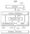
도 50을 참조하면, 도 1 내지 도 49를 참조하여 설명한 것과 유사한 반도체 소자는 전자 시스템(2100)에 적용될 수 있다. 상기 전자 시스템(2100)은 바디(Body; 2110), 마이크로프로세서 (MicroProcessor; 2120), 파워(Power; 2130), 기능 유닛(Function Unit; 2140), 및 디스플레이 컨트롤러(Display Controller; 2150)를 포함할 수 있다. 상기 바디(2110)는 인쇄 회로기판(PCB)으로 형성된 마더 보드(Mother Board)일 수 있다. 상기 마이크로프로세서(2120), 상기 파워(2130), 상기 기능 유닛(2140), 및 상기 디스플레이 컨트롤러(2150)는 상기 바디(2110)에 장착될 수 있다. 상기 바디(2110)의 내부 혹은 상기 바디(2110)의 외부에 디스플레이(2160)가 배치될 수 있다. 예를 들면, 상기 디스플레이(2160)는 상기 바디(2110)의 표면에 배치되어 상기 디스플레이 컨트롤러(2150)에 의해 프로세스 된 이미지를 표시할 수 있다.Referring to FIG. 50 , a semiconductor device similar to that described with reference to FIGS. 1 to 49 may be applied to the
상기 파워(2130)는 외부 배터리 등으로부터 일정 전압을 공급받아 이를 요구되는 전압 레벨로 분기하여 상기 마이크로프로세서(2120), 상기 기능 유닛(2140), 상기 디스플레이 컨트롤러(2150) 등으로 공급하는 역할을 할 수 있다. 상기 마이크로프로세서(2120)는 상기 파워(2130)로부터 전압을 공급받아 상기 기능 유닛(2140)과 상기 디스플레이(2160)를 제어할 수 있다. 상기 기능 유닛(2140)은 다양한 전자 시스템(2100)의 기능을 수행할 수 있다. 예를 들어, 상기 전자 시스템(2100)이 스마트 폰인 경우 상기 기능 유닛(2140)은 다이얼링, 또는 외부 장치(External Apparatus; 2170)와의 교신으로 상기 디스플레이(2160)로의 영상 출력, 스피커로의 음성 출력 등과 같은 휴대폰 기능을 수행할 수 있는 여러 구성요소들을 포함할 수 있으며, 카메라가 함께 장착된 경우 카메라 이미지 프로세서(Camera Image Processor)의 역할을 할 수 있다.The
응용 실시 예에서, 상기 전자 시스템(2100)이 용량 확장을 위해 메모리 카드 등과 연결되는 경우, 상기 기능 유닛(2140)은 메모리 카드 컨트롤러일 수 있다. 상기 기능 유닛(2140)은 유선 혹은 무선의 통신 유닛(Communication Unit; 2180)을 통해 상기 외부 장치(2170)와 신호를 주고 받을 수 있다. 더 나아가서, 상기 전자 시스템(2100)이 기능 확장을 위해 유에스비(Universal Serial Bus; USB) 등을 필요로 하는 경우, 상기 기능 유닛(2140)은 인터페이스 컨트롤러(Interface Controller)의 역할을 할 수 있다. 이에 더하여, 상기 기능 유닛(2140)은 대용량 저장 장치를 포함할 수 있다.In an application embodiment, when the
도 1 내지 도 49를 참조하여 설명한 것과 유사한 반도체 소자는 상기 기능 유닛(2140) 또는 상기 마이크로 프로세서(2120)에 적용될 수 있다. 예를 들면, 상기 마이크로프로세서(2120)는 상기 버퍼 막(45) 및 상기 제1 플러그 이온 주입 영역(75)을 포함할 수 있다.A semiconductor device similar to that described with reference to FIGS. 1 to 49 may be applied to the functional unit 2140 or the
도 51을 참조하면, 전자 시스템(2400)은 본 발명 기술적 사상의 다양한 실시 예들에 의한 반도체 소자들 중 적어도 하나를 포함할 수 있다. 전자 시스템(2400)은 모바일 기기 또는 컴퓨터를 제조하는데 사용될 수 있다. 예를 들어, 상기 전자 시스템(2400)은 메모리 시스템(2412), 마이크로프로세서(2414), 램(2416), 버스(2420), 및 유저 인터페이스(2418)를 포함할 수 있다. 상기 마이크로프로세서(2414), 상기 메모리 시스템(2412), 및 상기 유저 인터페이스(2418)는 상기 버스(2420)를 경유하여 상호 접속될 수 있다. 상기 유저 인터페이스(2418)는 상기 전자 시스템(2400)으로 데이터를 입력하거나 상기 전자 시스템(2400)으로부터 데이터를 출력하는데 사용될 수 있다. 상기 마이크로프로세서(2414)는 상기 전자 시스템(2400)을 프로그램 및 컨트롤할 수 있다. 상기 램(2416)은 상기 마이크로프로세서(2414)의 동작 메모리로 사용될 수 있다. 상기 마이크로프로세서(2414), 상기 램(2416) 및/또는 다른 구성 요소들은 단일 패키지 내에 조립될 수 있다. 상기 메모리 시스템(2412)은 상기 마이크로프로세서(2414) 동작용 코드들, 상기 마이크로프로세서(2414)에 의해 처리된 데이터, 또는 외부 입력 데이터를 저장할 수 있다. 상기 메모리 시스템(2412)은 컨트롤러 및 메모리를 포함할 수 있다.Referring to FIG. 51 , an
도 1 내지 도 49를 참조하여 설명한 것과 유사한 반도체 소자는 상기 마이크로프로세서(2414), 상기 램(2416), 또는 상기 메모리 시스템(2412)에 적용될 수 있다.A semiconductor device similar to that described with reference to FIGS. 1 to 49 may be applied to the
이상, 첨부된 도면을 참조하여 본 발명의 실시 예를 설명하였지만, 본 발명이 속하는 기술분야에서 통상의 지식을 가진 자는 본 발명이 그 기술적 사상이나 필수적인 특징을 변경하지 않고서 다른 구체적인 형태로 실시될 수 있다는 것을 이해할 수 있을 것이다. 그러므로 이상에서 기술한 실시 예에는 모든 면에서 예시적인 것이며 한정적이 아닌 것으로 이해해야만 한다.As mentioned above, although embodiments of the present invention have been described with reference to the accompanying drawings, those of ordinary skill in the art to which the present invention pertains can implement the present invention in other specific forms without changing its technical spirit or essential features. You can understand that there is Therefore, it should be understood that the embodiments described above are illustrative in all respects and not restrictive.
13: 반도체 기판21: N-웰
22: P-웰25: 소자 분리 막
27: N-형 핀28: P-형 핀
27R: 제1 리세스 영역28R: 제2 리세스 영역
31L: 가설 버퍼 막33L: 가설 게이트 막
35L: 가설 캐핑 막
31: 제1 가설 버퍼 패턴32: 제2 가설 버퍼 패턴
33: 제1 가설 게이트 패턴34: 제2 가설 게이트 패턴
33T: 제1 게이트 트렌치34T: 제2 게이트 트렌치
35: 제1 가설 캐핑 패턴36: 제2 가설 캐핑 패턴
37: 제1 내측 스페이서37A: 제1 하부 스페이서
38: 제2 내측 스페이서38A: 제2 하부 스페이서
43: 제1 소스/드레인43A: 제1 하부 반도체 막
43B: 제1 중간 반도체 막43C: 제1 상부 반도체 막
44, 44E: 제2 소스/드레인44D: 제2 하부 반도체 패턴
44C: 제2 상부 반도체 막45: 버퍼 막
47: 제1 외측 스페이서48: 제2 외측 스페이서
51: 제1 하부 절연 막52: 제2 하부 절연 막
52UC: 언더 컷 영역53: 식각 정지 막
61: 제1 하부 게이트 유전막62: 제2 하부 게이트 유전막
63: 제1 상부 게이트 유전막64: 제2 상부 게이트 유전막
65: 제1 하부 게이트 전극66: 제2 하부 게이트 전극
67: 제1 상부 게이트 전극68: 제2 상부 게이트 전극
69: 제1 게이트 전극70: 제2 게이트 전극
69R: 제1 게이트 리세스 영역70R: 제2 게이트 리세스 영역
71: 제1 게이트 캐핑 막72: 제2 게이트 캐핑 막
73: 제1 상부 절연 막74: 제2 상부 절연 막
73H: 제1 콘택 홀74H: 제2 콘택 홀
75: 제1 플러그 이온 주입 영역76: 제2 플러그 이온 주입 영역
81: 제1 금속 실리사이드 막82: 제2 금속 실리사이드 막
83: 제1 하부 도전 막84: 제2 하부 도전 막
85: 제1 상부 도전 막86: 제2 상부 도전 막
87: 제1 플러그88: 제2 플러그
2100: 전자 시스템
2110: 바디 2120: 마이크로 프로세서
2130: 파워2140: 기능 유닛
2150: 디스플레이 컨트롤러2160: 디스플레이
2170: 외부 장치2180: 통신 유닛
2400: 전자 시스템
2412: 메모리 시스템2414: 마이크로프로세서
2416: 램2418: 유저 인터페이스
2420: 버스13: semiconductor substrate 21: N-well
22: P-well 25: device isolation film
27: N-type pin 28: P-type pin
27R: first recessed
31L:
35L: Temporary capping membrane
31: first hypothesis buffer pattern 32: second hypothesis buffer pattern
33: first temporary gate pattern 34: second temporary gate pattern
33T:
35: first hypothetical capping pattern 36: second hypothetical capping pattern
37: first
38: second
43: first source/
43B: first
44, 44E: second source/
44C: second upper semiconductor film 45: buffer film
47: first outer spacer 48: second outer spacer
51: first lower insulating film 52: second lower insulating film
52UC: undercut area 53: etch stop film
61: first lower gate dielectric film 62: second lower gate dielectric film
63: first upper gate dielectric film 64: second upper gate dielectric film
65: first lower gate electrode 66: second lower gate electrode
67: first upper gate electrode 68: second upper gate electrode
69: first gate electrode 70: second gate electrode
69R: first
71: first gate capping film 72: second gate capping film
73: first upper insulating film 74: second upper insulating film
73H:
75: first plug ion implantation region 76: second plug ion implantation region
81: first metal silicide film 82: second metal silicide film
83: first lower conductive film 84: second lower conductive film
85: first upper conductive film 86: second upper conductive film
87: first plug 88: second plug
2100: electronic system
2110: body 2120: microprocessor
2130: power 2140: function unit
2150: display controller 2160: display
2170: external device 2180: communication unit
2400: electronic system
2412: memory system 2414: microprocessor
2416: ram 2418: user interface
2420: bus
Claims (20)
Translated fromKorean상기 N-형핀 상을 가로지르고 상기 N-형핀의 측면을 덮는 제1 게이트 전극 및 상기 P-형핀 상을 가로지르고 상기 P-형핀의 측면을 덮는 제2 게이트 전극;
상기 제1 게이트 전극에 인접한 상기 N-형핀 상에 형성된 제1 소스/드레인 및 상기 제2 게이트 전극에 인접한 상기 P-형핀 상에 형성된 제2 소스/드레인;
상기 제2 소스/드레인의 표면 상에 한정되고 상기 제2 소스/드레인과 다른 물질을 갖는 버퍼 막, 상기 버퍼 막은 상기 제1 소스/드레인의 표면은 모두 노출하되, 상기 제2 소스/드레인의 상기 표면의 일부를 덮고;
상기 버퍼 막 및 상기 제1 소스/드레인 상에 형성된 층간 절연 막;
상기 층간 절연 막을 관통하여 상기 제1 소스/드레인에 접속된 제1 플러그; 및
상기 층간 절연 막 및 상기 버퍼 막을 관통하여 상기 제2 소스/드레인에 접속된 제2 플러그를 포함하는 반도체소자.N-type and P-type pins defined on the substrate;
a first gate electrode crossing the N-type fin and covering a side surface of the N-type fin and a second gate electrode crossing the P-type fin and covering a side surface of the P-type fin;
a first source/drain formed on the N-type fin adjacent to the first gate electrode and a second source/drain formed on the P-type fin adjacent to the second gate electrode;
A buffer film defined on a surface of the second source/drain and having a material different from that of the second source/drain, wherein the buffer film exposes all surfaces of the first source/drain, wherein the surface of the second source/drain is covering part of the surface;
an interlayer insulating film formed on the buffer film and the first source/drain;
a first plug connected to the first source/drain through the interlayer insulating film; and
and a second plug connected to the second source/drain through the interlayer insulating layer and the buffer layer.
상기 제2 소스/드레인은 중심 영역의 수평 폭이 하부 영역의 수평 폭보다 크되, 상기 버퍼 막은 상기 제2 소스/드레인의 상기 하부 영역에 직접적으로 접촉된 반도체소자.According to claim 1,
A semiconductor device in which a horizontal width of a central region of the second source/drain is greater than a horizontal width of a lower region of the second source/drain, and the buffer layer is in direct contact with the lower region of the second source/drain.
상기 버퍼 막은 결정 성장된 물질을 포함하는 반도체소자.According to claim 1,
The buffer layer is a semiconductor device including a crystal-grown material.
상기 버퍼 막은 Ge를 포함하는 반도체소자.According to claim 1,
The buffer layer is a semiconductor device including Ge.
상기 제1 소스/드레인 및 상기 제1 플러그 사이에 형성된 플러그 이온 주입 영역을 더 포함하되,
상기 플러그 이온 주입 영역의 P-형 불순물 농도는 상기 제1 소스/드레인 보다 큰 반도체소자.According to claim 1,
a plug ion implantation region formed between the first source/drain and the first plug;
A P-type impurity concentration of the plug ion implantation region is greater than that of the first source/drain.
상기 버퍼 막은 상기 플러그 이온 주입 영역 보다 두꺼운 반도체소자.6. The method of claim 5,
The buffer layer is thicker than the plug ion implantation region.
상기 버퍼 막의 두께는 3 nm 이상이되, 상기 층간 절연 막보다 얇은 반도체소자.According to claim 1,
The thickness of the buffer layer is 3 nm or more, the semiconductor device is thinner than the interlayer insulating layer.
상기 제1 소스/드레인은 SiGe, Si, B, BF, 또는 이들의 조합을 포함하고, 상기 제2 소스/드레인은 SiC, Si, P, As, 또는 이들의 조합을 포함하는 반도체소자.According to claim 1,
The first source/drain may include SiGe, Si, B, BF, or a combination thereof, and the second source/drain may include SiC, Si, P, As, or a combination thereof.
상기 제2 플러그는 하단의 수평 폭이 중심의 수평 폭보다 큰 반도체소자.According to claim 1,
The second plug is a semiconductor device having a lower horizontal width greater than a central horizontal width.
상기 층간 절연 막의 하부에 형성된 언더-컷(under-cut) 영역을 더 포함하되, 상기 제2 플러그는 상기 언더-컷(under-cut) 영역 내에 신장되고, 상기 제2 플러그는 상기 버퍼 막에 접촉된 반도체소자.According to claim 1,
an under-cut region formed under the interlayer insulating film, wherein the second plug extends within the under-cut region, and the second plug contacts the buffer film semiconductor device.
상기 제1 플러그 및 상기 제1 소스/드레인 사이와 상기 제2 플러그 및 상기 제2 소스/드레인 사이에 형성된 금속 실리사이드 막들을 더 포함하는 반도체소자.According to claim 1,
and metal silicide layers formed between the first plug and the first source/drain and between the second plug and the second source/drain.
상기 제1 도전형핀 상을 가로지르고 상기 제1 도전형핀의 측면을 덮는 제1 게이트 전극;
상기 제1 게이트 전극에 인접한 상기 제1 도전형핀 상에 형성된 제2도전형 소스/드레인;
상기 제2도전형 소스/드레인 상에서 상기 제1 게이트 전극의 측면들을 덮는 스페이서;
상기 제2도전형 소스/드레인의 표면 상에 한정되고 상기 제2도전형 소스/드레인과 다른 물질을 갖는 버퍼 막;
상기 버퍼 막 상에 형성된 층간 절연 막; 및
상기 층간 절연 막 및 상기 버퍼 막을 관통하여 상기 제2도전형 소스/드레인에 접속된 제1 플러그를 포함하되,
상기 제2도전형은 상기 제1 도전형과 다른 도전형이고,
상기 버퍼 막은 상기 스페이서와 상기 제2도전형 소스/드레인 사이에 제공되는 반도체소자.a first conductive type pin defined on the substrate;
a first gate electrode crossing over the first conductivity type fin and covering a side surface of the first conductivity type fin;
a second conductivity type source/drain formed on the first conductivity type fin adjacent to the first gate electrode;
a spacer covering side surfaces of the first gate electrode on the second conductivity type source/drain;
a buffer film defined on a surface of the second conductivity type source/drain and having a material different from that of the second conductivity type source/drain;
an interlayer insulating film formed on the buffer film; and
a first plug connected to the second conductive type source/drain through the interlayer insulating layer and the buffer layer;
The second conductivity type is a conductivity type different from the first conductivity type,
The buffer layer is provided between the spacer and the second conductivity type source/drain semiconductor device.
상기 기판 상에 한정되고 상기 제1 도전형핀과 떨어진 제2 도전형핀;
상기 제2 도전형핀 상을 가로지르고 상기 제2 도전형핀의 측면을 덮는 제2 게이트 전극;
상기 제2 게이트 전극에 인접한 상기 제2 도전형핀 상에 형성된 제1도전형 소스/드레인; 및
상기 층간 절연 막을 관통하여 상기 제1도전형 소스/드레인에 접속된 제2 플러그를 더 포함하되,
상기 층간 절연 막은 상기 제1도전형 소스/드레인 상에 형성된 반도체소자.13. The method of claim 12,
a second conductivity type fin defined on the substrate and separated from the first conductivity type fin;
a second gate electrode crossing over the second conductivity type fin and covering a side surface of the second conductivity type fin;
a first conductivity type source/drain formed on the second conductivity type fin adjacent to the second gate electrode; and
Further comprising a second plug connected to the first conductive type source/drain through the interlayer insulating film,
The interlayer insulating layer is a semiconductor device formed on the first conductive type source/drain.
상기 제1도전형 소스/드레인 및 상기 제2 플러그 사이에 형성된 플러그 이온 주입 영역을 더 포함하는 반도체소자.14. The method of claim 13,
and a plug ion implantation region formed between the first conductive type source/drain and the second plug.
상기 버퍼 막은 상기 플러그 이온 주입 영역 보다 두꺼운 반도체소자.15. The method of claim 14,
The buffer layer is thicker than the plug ion implantation region.
상기 제1 도전형핀들 상을 가로지르고 상기 제1 도전형핀들의 측면들을 덮는 제1 게이트 전극;
상기 제1 게이트 전극에 인접한 상기 제1 도전형핀들 상에 형성된 제2도전형 소스/드레인들;
상기 제2도전형 소스/드레인을 향하는 상기 제1 게이트 전극의 측면들을 덮는 스페이서;
상기 제2도전형 소스/드레인들의 표면 상에 한정되고 상기 제2도전형 소스/드레인들과 다른 물질을 갖는 버퍼 막;
상기 버퍼 막 상에 형성된 층간 절연 막; 및
상기 층간 절연 막 및 상기 버퍼 막을 관통하여 상기 제2도전형 소스/드레인들에 접속된 제1 플러그를 포함하되,
상기 제2도전형은 상기 제1 도전형과 다른 도전형이고,
상기 층간 절연 막의 하부에서 상기 스페이서와 상기 제2도전형 소스/드레인 사이에 형성된 언더-컷(under-cut) 영역을 더 포함하되, 상기 제1 플러그는 상기 언더-컷(under-cut) 영역 내에 신장되어 상기 버퍼 막에 접촉된 반도체소자.a plurality of first conductivity type fins defined on the substrate and parallel to each other;
a first gate electrode crossing over the first conductivity type fins and covering side surfaces of the first conductivity type fins;
second conductivity type sources/drains formed on the first conductivity type fins adjacent to the first gate electrode;
a spacer covering side surfaces of the first gate electrode facing the second conductivity type source/drain;
a buffer film defined on the surfaces of the second conductivity type sources/drains and having a material different from that of the second conductivity type sources/drains;
an interlayer insulating film formed on the buffer film; and
a first plug passing through the interlayer insulating layer and the buffer layer and connected to the second conductive type source/drains;
The second conductivity type is a conductivity type different from the first conductivity type,
An under-cut region formed between the spacer and the second conductive type source/drain under the interlayer insulating layer, wherein the first plug is in the under-cut region A semiconductor device that is stretched and is in contact with the buffer layer.
상기 기판 상에 한정되고 상기 제1 도전형핀들과 떨어지며 서로 평행한다수의 제2 도전형핀들;
상기 제2 도전형핀들 상을 가로지르고 상기 제2 도전형핀들의 측면들을 덮는 제2 게이트 전극;
상기 제2 게이트 전극에 인접한 상기 제2 도전형핀들 상에 형성된 제1도전형 소스/드레인들; 및
상기 층간 절연 막을 관통하여 상기 제1도전형 소스/드레인들에 접속된 제2 플러그를 더 포함하되,
상기 층간 절연 막은 상기 제1도전형 소스/드레인들 상에 형성된 반도체소자.17. The method of claim 16,
a plurality of second conductivity type fins defined on the substrate and spaced apart from the first conductivity type fins and parallel to each other;
a second gate electrode crossing over the second conductivity type fins and covering side surfaces of the second conductivity type fins;
first conductivity type sources/drains formed on the second conductivity type fins adjacent to the second gate electrode; and
Further comprising a second plug connected to the first conductive type source / drain through the interlayer insulating film,
The interlayer insulating layer is a semiconductor device formed on the first conductivity type source/drains.
상기 제1도전형 소스/드레인들 및 상기 제2 플러그 사이에 형성된 플러그 이온 주입 영역을 더 포함하는 반도체소자.18. The method of claim 17,
The semiconductor device further comprising a plug ion implantation region formed between the first conductive type source/drain and the second plug.
상기 제1 도전형핀 상을 가로지르고 상기 제1 도전형핀의 측면을 덮는 제1 게이트 전극 및 상기 제2 도전형핀 상을 가로지르고 상기 제2 도전형핀의 측면을 덮는 제2 게이트 전극을 형성하고,
상기 제1 게이트 전극에 인접한 상기 제1 도전형핀 상에 제2 도전형 소스/드레인 및 상기 제2 게이트 전극에 인접한 상기 제2 도전형핀 상에 제1 도전형 소스/드레인을 형성하고,
상기 제1 도전형 소스/드레인의 표면 상에 한정되고 상기 제1 도전형 소스/드레인과 다른 물질을 갖는 버퍼 막을 형성하되, 상기 버퍼 막은 상기 제1 도전형 소스/드레인의 상기 표면을 모두 덮고,
상기 버퍼 막 및 상기 제2 도전형 소스/드레인 상에 층간 절연 막을 형성하고,
상기 층간 절연 막을 관통하여 상기 제2 도전형 소스/드레인에 접속된 제1 플러그 및 상기 층간 절연 막 및 상기 버퍼 막을 관통하여 상기 제1 도전형 소스/드레인에 접속된 제2 플러그를 형성하는 것을 포함하는 반도체소자 형성 방법.Forming a first conductivity-type fin and a second conductivity-type fin on a substrate,
forming a first gate electrode crossing over the first conductivity type fin and covering a side surface of the first conductivity type fin and a second gate electrode crossing over the second conductivity type fin and covering a side surface of the second conductivity type fin;
forming a second conductivity type source/drain on the first conductivity type fin adjacent to the first gate electrode and a first conductivity type source/drain on the second conductivity type fin adjacent to the second gate electrode;
A buffer film defined on a surface of the first conductivity type source/drain and having a material different from that of the first conductivity type source/drain, wherein the buffer film covers all the surfaces of the first conductivity type source/drain;
forming an interlayer insulating film on the buffer film and the second conductivity type source/drain;
forming a first plug connected to the second conductivity type source/drain through the interlayer insulating film and a second plug connected to the first conductivity type source/drain through the interlayer insulating film and the buffer film A method of forming a semiconductor device.
상기 제1 플러그 및 상기 제2 플러그를 형성하는 것은
상기 층간 절연 막을 관통하여 상기 제2 도전형 소스/드레인을 노출하는 제1 콘택 홀 및 상기 층간 절연 막을 관통하여 상기 버퍼 막을 노출하는 제2 콘택 홀을 형성하고,
상기 제2 도전형 소스/드레인 내에 제2 도전형 불순물들을 주입하여 플러그 이온 주입 영역을 형성하고,
상기 제2 콘택 홀에 노출된 상기 버퍼 막을 제거하여 상기 제1 도전형 소스/드레인을 노출하는 것을 더 포함하는 반도체소자 형성 방법.20. The method of claim 19,
Forming the first plug and the second plug
forming a first contact hole exposing the second conductivity type source/drain through the interlayer insulating layer and a second contact hole exposing the buffer layer through the interlayer insulating layer;
forming a plug ion implantation region by implanting second conductivity type impurities into the second conductivity type source/drain;
and exposing the source/drain of the first conductivity type by removing the buffer layer exposed through the second contact hole.
Priority Applications (3)
| Application Number | Priority Date | Filing Date | Title |
|---|---|---|---|
| KR1020140127083AKR102311937B1 (en) | 2014-09-23 | 2014-09-23 | Semiconductor device having contact plug and method of forming the same |
| US14/714,711US9331080B2 (en) | 2014-09-23 | 2015-05-18 | Semiconductor device having contact plug and method of forming the same |
| CN201510603877.4ACN105448911B (en) | 2014-09-23 | 2015-09-21 | Semiconductor device with contact plug |
Applications Claiming Priority (1)
| Application Number | Priority Date | Filing Date | Title |
|---|---|---|---|
| KR1020140127083AKR102311937B1 (en) | 2014-09-23 | 2014-09-23 | Semiconductor device having contact plug and method of forming the same |
Publications (2)
| Publication Number | Publication Date |
|---|---|
| KR20160035453A KR20160035453A (en) | 2016-03-31 |
| KR102311937B1true KR102311937B1 (en) | 2021-10-14 |
Family
ID=55526466
Family Applications (1)
| Application Number | Title | Priority Date | Filing Date |
|---|---|---|---|
| KR1020140127083AActiveKR102311937B1 (en) | 2014-09-23 | 2014-09-23 | Semiconductor device having contact plug and method of forming the same |
Country Status (3)
| Country | Link |
|---|---|
| US (1) | US9331080B2 (en) |
| KR (1) | KR102311937B1 (en) |
| CN (1) | CN105448911B (en) |
Families Citing this family (18)
| Publication number | Priority date | Publication date | Assignee | Title |
|---|---|---|---|---|
| KR102422430B1 (en)* | 2015-07-16 | 2022-07-18 | 삼성전자주식회사 | Semiconductor device and fabricating method thereof |
| US10103249B2 (en) | 2015-09-10 | 2018-10-16 | Taiwan Semiconductor Manufacturing Co., Ltd. | FinFET device and method for fabricating the same |
| CN107564953B (en)* | 2016-07-01 | 2021-07-30 | 中芯国际集成电路制造(上海)有限公司 | Varactor transistor and method of making the same |
| KR102620597B1 (en) | 2016-09-23 | 2024-01-03 | 삼성전자주식회사 | Semiconductor device |
| US10164042B2 (en)* | 2016-11-29 | 2018-12-25 | Taiwan Semiconductor Manufacturing Co., Ltd. | Semiconductor device and manufacturing method thereof |
| EP3920212B1 (en) | 2016-12-30 | 2025-10-01 | INTEL Corporation | Contact architecture for capacitance reduction and satisfactory contact resistance and corresponding method |
| CN109119350B (en)* | 2017-06-23 | 2021-03-09 | 中芯国际集成电路制造(上海)有限公司 | Semiconductor structure, forming method thereof and method for measuring resistance |
| US10510875B2 (en)* | 2017-07-31 | 2019-12-17 | Taiwan Semiconductor Manufacturing Co., Ltd. | Source and drain structure with reduced contact resistance and enhanced mobility |
| US10763168B2 (en)* | 2017-11-17 | 2020-09-01 | Taiwan Semiconductor Manufacturing Co., Ltd. | Semiconductor structure with doped via plug and method for forming the same |
| US10658362B2 (en)* | 2017-11-27 | 2020-05-19 | Taiwan Semiconductor Manufacturing Co., Ltd. | Semiconductor component and fabricating method thereof |
| KR102524803B1 (en)* | 2018-11-14 | 2023-04-24 | 삼성전자주식회사 | Semiconductor device including source/drain region |
| US11257928B2 (en)* | 2018-11-27 | 2022-02-22 | Taiwan Semiconductor Manufacturing Company, Ltd. | Method for epitaxial growth and device |
| US11374101B2 (en)* | 2019-02-28 | 2022-06-28 | Tokyo Electron Limited | Dual metal wrap-around contacts for semiconductor devices |
| US11652107B2 (en)* | 2019-06-20 | 2023-05-16 | Intel Corporation | Substrate-less FinFET diode architectures with backside metal contact and subfin regions |
| KR102807501B1 (en)* | 2019-10-02 | 2025-05-16 | 삼성전자주식회사 | Semiconductor devices including a thick metal layer |
| KR20210073142A (en)* | 2019-12-10 | 2021-06-18 | 삼성전자주식회사 | Semiconductor devices |
| CN113113311A (en)* | 2020-02-27 | 2021-07-13 | 台湾积体电路制造股份有限公司 | Method for forming semiconductor device |
| KR102784272B1 (en)* | 2020-04-20 | 2025-03-24 | 삼성전자주식회사 | Semiconductor device |
Citations (1)
| Publication number | Priority date | Publication date | Assignee | Title |
|---|---|---|---|---|
| CN101882594A (en)* | 2009-05-05 | 2010-11-10 | 中芯国际集成电路制造(上海)有限公司 | Forming method of conductive plug |
Family Cites Families (11)
| Publication number | Priority date | Publication date | Assignee | Title |
|---|---|---|---|---|
| US8994104B2 (en) | 1999-09-28 | 2015-03-31 | Intel Corporation | Contact resistance reduction employing germanium overlayer pre-contact metalization |
| JP2009054705A (en) | 2007-08-24 | 2009-03-12 | Toshiba Corp | Semiconductor substrate, semiconductor device and manufacturing method thereof |
| KR20090083671A (en)* | 2008-01-30 | 2009-08-04 | 주식회사 하이닉스반도체 | Manufacturing method of semiconductor device |
| US9245805B2 (en) | 2009-09-24 | 2016-01-26 | Taiwan Semiconductor Manufacturing Company, Ltd. | Germanium FinFETs with metal gates and stressors |
| KR101891458B1 (en)* | 2011-12-20 | 2018-08-24 | 인텔 코포레이션 | Semiconductor device having iii-v semiconductor material layer |
| US8486770B1 (en)* | 2011-12-30 | 2013-07-16 | Taiwan Semiconductor Manufacturing Company, Ltd. | Method of forming CMOS FinFET device |
| US8377779B1 (en)* | 2012-01-03 | 2013-02-19 | Taiwan Semiconductor Manufacturing Company, Ltd. | Methods of manufacturing semiconductor devices and transistors |
| US8476706B1 (en) | 2012-01-04 | 2013-07-02 | International Business Machines Corporation | CMOS having a SiC/SiGe alloy stack |
| US9041115B2 (en)* | 2012-05-03 | 2015-05-26 | Taiwan Semiconductor Manufacturing Company, Ltd. | Structure for FinFETs |
| US8772109B2 (en)* | 2012-10-24 | 2014-07-08 | Taiwan Semiconductor Manufacturing Company, Ltd. | Apparatus and method for forming semiconductor contacts |
| CN104124174B (en)* | 2013-04-28 | 2017-02-22 | 中芯国际集成电路制造(上海)有限公司 | Semiconductor structure and forming method thereof |
- 2014
- 2014-09-23KRKR1020140127083Apatent/KR102311937B1/enactiveActive
- 2015
- 2015-05-18USUS14/714,711patent/US9331080B2/enactiveActive
- 2015-09-21CNCN201510603877.4Apatent/CN105448911B/enactiveActive
Patent Citations (1)
| Publication number | Priority date | Publication date | Assignee | Title |
|---|---|---|---|---|
| CN101882594A (en)* | 2009-05-05 | 2010-11-10 | 中芯国际集成电路制造(上海)有限公司 | Forming method of conductive plug |
Also Published As
| Publication number | Publication date |
|---|---|
| KR20160035453A (en) | 2016-03-31 |
| CN105448911B (en) | 2021-03-02 |
| CN105448911A (en) | 2016-03-30 |
| US20160086950A1 (en) | 2016-03-24 |
| US9331080B2 (en) | 2016-05-03 |
Similar Documents
| Publication | Publication Date | Title |
|---|---|---|
| KR102311937B1 (en) | Semiconductor device having contact plug and method of forming the same | |
| KR102282980B1 (en) | Semiconductor device having silicide and method of forming the same | |
| KR102178831B1 (en) | Method of forming semiconductor device having stressor and related device | |
| KR101909204B1 (en) | Semiconductor device having embedded strain-inducing pattern and method of forming the same | |
| KR102059526B1 (en) | Method of forming semiconductor device having embedded stressor and related device | |
| US10861748B2 (en) | Semiconductor arrangement and method for manufacturing the same | |
| US9257520B2 (en) | Semiconductor devices including a stressor in a recess and methods of forming the same | |
| KR102255174B1 (en) | Semiconductor device having active region and method of forming the same | |
| KR102152285B1 (en) | Semiconductor device having stressor and method of forming the same | |
| KR102415327B1 (en) | Semiconductor device having inactive-fin and method of forming the same | |
| KR20160144164A (en) | Semiconductor device blocking a leakage current and method for fabricating the same | |
| KR20150105866A (en) | Semiconductor device having stressor and method of forming the same | |
| KR102117978B1 (en) | Method of forming semiconductor device having embedded stressor and related apparatus | |
| US9559102B2 (en) | Semiconductor device | |
| KR102200922B1 (en) | Semiconductor device having insulating pattern and method of forming the same | |
| KR102192571B1 (en) | Semiconductor device having buffer layer and method of forming the same | |
| KR102814859B1 (en) | Semiconductor device | |
| KR102037864B1 (en) | Semiconductor device having embedded stressor and method of forming the same |
Legal Events
| Date | Code | Title | Description |
|---|---|---|---|
| PA0109 | Patent application | St.27 status event code:A-0-1-A10-A12-nap-PA0109 | |
| PG1501 | Laying open of application | St.27 status event code:A-1-1-Q10-Q12-nap-PG1501 | |
| R17-X000 | Change to representative recorded | St.27 status event code:A-3-3-R10-R17-oth-X000 | |
| R17-X000 | Change to representative recorded | St.27 status event code:A-3-3-R10-R17-oth-X000 | |
| R17-X000 | Change to representative recorded | St.27 status event code:A-3-3-R10-R17-oth-X000 | |
| PA0201 | Request for examination | St.27 status event code:A-1-2-D10-D11-exm-PA0201 | |
| E902 | Notification of reason for refusal | ||
| PE0902 | Notice of grounds for rejection | St.27 status event code:A-1-2-D10-D21-exm-PE0902 | |
| P11-X000 | Amendment of application requested | St.27 status event code:A-2-2-P10-P11-nap-X000 | |
| P13-X000 | Application amended | St.27 status event code:A-2-2-P10-P13-nap-X000 | |
| E90F | Notification of reason for final refusal | ||
| PE0902 | Notice of grounds for rejection | St.27 status event code:A-1-2-D10-D21-exm-PE0902 | |
| P11-X000 | Amendment of application requested | St.27 status event code:A-2-2-P10-P11-nap-X000 | |
| P13-X000 | Application amended | St.27 status event code:A-2-2-P10-P13-nap-X000 | |
| E701 | Decision to grant or registration of patent right | ||
| PE0701 | Decision of registration | St.27 status event code:A-1-2-D10-D22-exm-PE0701 | |
| GRNT | Written decision to grant | ||
| PR0701 | Registration of establishment | St.27 status event code:A-2-4-F10-F11-exm-PR0701 | |
| PR1002 | Payment of registration fee | St.27 status event code:A-2-2-U10-U11-oth-PR1002 Fee payment year number:1 | |
| PG1601 | Publication of registration | St.27 status event code:A-4-4-Q10-Q13-nap-PG1601 | |
| PR1001 | Payment of annual fee | St.27 status event code:A-4-4-U10-U11-oth-PR1001 Fee payment year number:4 | |
| P22-X000 | Classification modified | St.27 status event code:A-4-4-P10-P22-nap-X000 | |
| PR1001 | Payment of annual fee | St.27 status event code:A-4-4-U10-U11-oth-PR1001 Fee payment year number:5 |