KR102307633B1 - Semiconductor device and method for manufacturing the same - Google Patents
Semiconductor device and method for manufacturing the sameDownload PDFInfo
- Publication number
- KR102307633B1 KR102307633B1KR1020140177548AKR20140177548AKR102307633B1KR 102307633 B1KR102307633 B1KR 102307633B1KR 1020140177548 AKR1020140177548 AKR 1020140177548AKR 20140177548 AKR20140177548 AKR 20140177548AKR 102307633 B1KR102307633 B1KR 102307633B1
- Authority
- KR
- South Korea
- Prior art keywords
- contact
- conductive pattern
- insulating layer
- contact hole
- opening
- Prior art date
- Legal status (The legal status is an assumption and is not a legal conclusion. Google has not performed a legal analysis and makes no representation as to the accuracy of the status listed.)
- Active
Links
Images


Classifications
- H—ELECTRICITY
- H10—SEMICONDUCTOR DEVICES; ELECTRIC SOLID-STATE DEVICES NOT OTHERWISE PROVIDED FOR
- H10D—INORGANIC ELECTRIC SEMICONDUCTOR DEVICES
- H10D30/00—Field-effect transistors [FET]
- H10D30/60—Insulated-gate field-effect transistors [IGFET]
- H10D30/69—IGFETs having charge trapping gate insulators, e.g. MNOS transistors
- H10D30/694—IGFETs having charge trapping gate insulators, e.g. MNOS transistors characterised by the shapes, relative sizes or dispositions of the gate electrodes
- H—ELECTRICITY
- H10—SEMICONDUCTOR DEVICES; ELECTRIC SOLID-STATE DEVICES NOT OTHERWISE PROVIDED FOR
- H10B—ELECTRONIC MEMORY DEVICES
- H10B41/00—Electrically erasable-and-programmable ROM [EEPROM] devices comprising floating gates
- H10B41/20—Electrically erasable-and-programmable ROM [EEPROM] devices comprising floating gates characterised by three-dimensional arrangements, e.g. with cells on different height levels
- H10B41/23—Electrically erasable-and-programmable ROM [EEPROM] devices comprising floating gates characterised by three-dimensional arrangements, e.g. with cells on different height levels with source and drain on different levels, e.g. with sloping channels
- H10B41/27—Electrically erasable-and-programmable ROM [EEPROM] devices comprising floating gates characterised by three-dimensional arrangements, e.g. with cells on different height levels with source and drain on different levels, e.g. with sloping channels the channels comprising vertical portions, e.g. U-shaped channels
- H—ELECTRICITY
- H01—ELECTRIC ELEMENTS
- H01L—SEMICONDUCTOR DEVICES NOT COVERED BY CLASS H10
- H01L21/00—Processes or apparatus adapted for the manufacture or treatment of semiconductor or solid state devices or of parts thereof
- H01L21/70—Manufacture or treatment of devices consisting of a plurality of solid state components formed in or on a common substrate or of parts thereof; Manufacture of integrated circuit devices or of parts thereof
- H01L21/71—Manufacture of specific parts of devices defined in group H01L21/70
- H01L21/768—Applying interconnections to be used for carrying current between separate components within a device comprising conductors and dielectrics
- H01L21/76801—Applying interconnections to be used for carrying current between separate components within a device comprising conductors and dielectrics characterised by the formation and the after-treatment of the dielectrics, e.g. smoothing
- H01L21/76802—Applying interconnections to be used for carrying current between separate components within a device comprising conductors and dielectrics characterised by the formation and the after-treatment of the dielectrics, e.g. smoothing by forming openings in dielectrics
- H01L21/76805—Applying interconnections to be used for carrying current between separate components within a device comprising conductors and dielectrics characterised by the formation and the after-treatment of the dielectrics, e.g. smoothing by forming openings in dielectrics the opening being a via or contact hole penetrating the underlying conductor
- H—ELECTRICITY
- H01—ELECTRIC ELEMENTS
- H01L—SEMICONDUCTOR DEVICES NOT COVERED BY CLASS H10
- H01L21/00—Processes or apparatus adapted for the manufacture or treatment of semiconductor or solid state devices or of parts thereof
- H01L21/70—Manufacture or treatment of devices consisting of a plurality of solid state components formed in or on a common substrate or of parts thereof; Manufacture of integrated circuit devices or of parts thereof
- H01L21/71—Manufacture of specific parts of devices defined in group H01L21/70
- H01L21/768—Applying interconnections to be used for carrying current between separate components within a device comprising conductors and dielectrics
- H01L21/76801—Applying interconnections to be used for carrying current between separate components within a device comprising conductors and dielectrics characterised by the formation and the after-treatment of the dielectrics, e.g. smoothing
- H01L21/76802—Applying interconnections to be used for carrying current between separate components within a device comprising conductors and dielectrics characterised by the formation and the after-treatment of the dielectrics, e.g. smoothing by forming openings in dielectrics
- H01L21/76816—Aspects relating to the layout of the pattern or to the size of vias or trenches
- H—ELECTRICITY
- H01—ELECTRIC ELEMENTS
- H01L—SEMICONDUCTOR DEVICES NOT COVERED BY CLASS H10
- H01L23/00—Details of semiconductor or other solid state devices
- H01L23/28—Encapsulations, e.g. encapsulating layers, coatings, e.g. for protection
- H01L23/31—Encapsulations, e.g. encapsulating layers, coatings, e.g. for protection characterised by the arrangement or shape
- H01L23/3157—Partial encapsulation or coating
- H01L23/3171—Partial encapsulation or coating the coating being directly applied to the semiconductor body, e.g. passivation layer
- H—ELECTRICITY
- H01—ELECTRIC ELEMENTS
- H01L—SEMICONDUCTOR DEVICES NOT COVERED BY CLASS H10
- H01L23/00—Details of semiconductor or other solid state devices
- H01L23/48—Arrangements for conducting electric current to or from the solid state body in operation, e.g. leads, terminal arrangements ; Selection of materials therefor
- H01L23/482—Arrangements for conducting electric current to or from the solid state body in operation, e.g. leads, terminal arrangements ; Selection of materials therefor consisting of lead-in layers inseparably applied to the semiconductor body (electrodes)
- H01L23/485—Arrangements for conducting electric current to or from the solid state body in operation, e.g. leads, terminal arrangements ; Selection of materials therefor consisting of lead-in layers inseparably applied to the semiconductor body (electrodes) consisting of layered constructions comprising conductive layers and insulating layers, e.g. planar contacts
- H—ELECTRICITY
- H01—ELECTRIC ELEMENTS
- H01L—SEMICONDUCTOR DEVICES NOT COVERED BY CLASS H10
- H01L23/00—Details of semiconductor or other solid state devices
- H01L23/52—Arrangements for conducting electric current within the device in operation from one component to another, i.e. interconnections, e.g. wires, lead frames
- H01L23/522—Arrangements for conducting electric current within the device in operation from one component to another, i.e. interconnections, e.g. wires, lead frames including external interconnections consisting of a multilayer structure of conductive and insulating layers inseparably formed on the semiconductor body
- H01L23/5226—Via connections in a multilevel interconnection structure
- H—ELECTRICITY
- H10—SEMICONDUCTOR DEVICES; ELECTRIC SOLID-STATE DEVICES NOT OTHERWISE PROVIDED FOR
- H10B—ELECTRONIC MEMORY DEVICES
- H10B43/00—EEPROM devices comprising charge-trapping gate insulators
- H10B43/20—EEPROM devices comprising charge-trapping gate insulators characterised by three-dimensional arrangements, e.g. with cells on different height levels
- H10B43/23—EEPROM devices comprising charge-trapping gate insulators characterised by three-dimensional arrangements, e.g. with cells on different height levels with source and drain on different levels, e.g. with sloping channels
- H10B43/27—EEPROM devices comprising charge-trapping gate insulators characterised by three-dimensional arrangements, e.g. with cells on different height levels with source and drain on different levels, e.g. with sloping channels the channels comprising vertical portions, e.g. U-shaped channels
- H—ELECTRICITY
- H10—SEMICONDUCTOR DEVICES; ELECTRIC SOLID-STATE DEVICES NOT OTHERWISE PROVIDED FOR
- H10B—ELECTRONIC MEMORY DEVICES
- H10B43/00—EEPROM devices comprising charge-trapping gate insulators
- H10B43/30—EEPROM devices comprising charge-trapping gate insulators characterised by the memory core region
- H10B43/35—EEPROM devices comprising charge-trapping gate insulators characterised by the memory core region with cell select transistors, e.g. NAND
- H—ELECTRICITY
- H10—SEMICONDUCTOR DEVICES; ELECTRIC SOLID-STATE DEVICES NOT OTHERWISE PROVIDED FOR
- H10B—ELECTRONIC MEMORY DEVICES
- H10B43/00—EEPROM devices comprising charge-trapping gate insulators
- H10B43/50—EEPROM devices comprising charge-trapping gate insulators characterised by the boundary region between the core and peripheral circuit regions
- H—ELECTRICITY
- H10—SEMICONDUCTOR DEVICES; ELECTRIC SOLID-STATE DEVICES NOT OTHERWISE PROVIDED FOR
- H10D—INORGANIC ELECTRIC SEMICONDUCTOR DEVICES
- H10D30/00—Field-effect transistors [FET]
- H10D30/01—Manufacture or treatment
- H10D30/021—Manufacture or treatment of FETs having insulated gates [IGFET]
- H10D30/0413—Manufacture or treatment of FETs having insulated gates [IGFET] of FETs having charge-trapping gate insulators, e.g. MNOS transistors
- H—ELECTRICITY
- H10—SEMICONDUCTOR DEVICES; ELECTRIC SOLID-STATE DEVICES NOT OTHERWISE PROVIDED FOR
- H10D—INORGANIC ELECTRIC SEMICONDUCTOR DEVICES
- H10D30/00—Field-effect transistors [FET]
- H10D30/60—Insulated-gate field-effect transistors [IGFET]
- H10D30/69—IGFETs having charge trapping gate insulators, e.g. MNOS transistors
- H10D30/693—Vertical IGFETs having charge trapping gate insulators
- H—ELECTRICITY
- H10—SEMICONDUCTOR DEVICES; ELECTRIC SOLID-STATE DEVICES NOT OTHERWISE PROVIDED FOR
- H10D—INORGANIC ELECTRIC SEMICONDUCTOR DEVICES
- H10D64/00—Electrodes of devices having potential barriers
- H10D64/01—Manufacture or treatment
- H10D64/031—Manufacture or treatment of data-storage electrodes
- H10D64/037—Manufacture or treatment of data-storage electrodes comprising charge-trapping insulators
- H—ELECTRICITY
- H01—ELECTRIC ELEMENTS
- H01L—SEMICONDUCTOR DEVICES NOT COVERED BY CLASS H10
- H01L2924/00—Indexing scheme for arrangements or methods for connecting or disconnecting semiconductor or solid-state bodies as covered by H01L24/00
- H01L2924/0001—Technical content checked by a classifier
- H01L2924/0002—Not covered by any one of groups H01L24/00, H01L24/00 and H01L2224/00
Landscapes
- Engineering & Computer Science (AREA)
- Physics & Mathematics (AREA)
- Condensed Matter Physics & Semiconductors (AREA)
- General Physics & Mathematics (AREA)
- Computer Hardware Design (AREA)
- Microelectronics & Electronic Packaging (AREA)
- Power Engineering (AREA)
- Manufacturing & Machinery (AREA)
- Semiconductor Memories (AREA)
- Internal Circuitry In Semiconductor Integrated Circuit Devices (AREA)
- Geometry (AREA)
Abstract
Translated fromKoreanDescription
Translated fromKorean본 발명은 반도체 소자 및 그 제조 방법에 관한 것으로, 보다 상세하게는 콘택 플러그를 포함하는 반도체 소자 및 그 제조 방법에 관한 것이다.The present invention relates to a semiconductor device and a method for manufacturing the same, and more particularly, to a semiconductor device including a contact plug and a method for manufacturing the same.
전자 제품은 그 부피가 점점 작아지면서도 고용량의 데이터 처리를 요하고 있다. 이에 따라, 이러한 전자 제품에 사용되는 반도체 메모리 소자의 집적도를 증가시킬 필요가 있다. 반도체 메모리 소자의 집적도를 향상시키기 위한 방법들 중 하나로서, 기존의 평면 트랜지스터 구조 대신 수직 트랜지스터 구조를 가지는 비휘발성 메모리 소자가 제안되고 있다. 이러한 수직 트랜지스터 구조를 가지는 비휘발성 메모리 소자에서는, 서로 다른 레벨을 가지는 복수 개의 전극에 동시에 콘택 플러그가 형성되어야 한다.Electronic products require high-capacity data processing while their volume is getting smaller. Accordingly, it is necessary to increase the degree of integration of semiconductor memory devices used in such electronic products. As one of methods for improving the degree of integration of a semiconductor memory device, a nonvolatile memory device having a vertical transistor structure instead of a conventional planar transistor structure has been proposed. In a nonvolatile memory device having such a vertical transistor structure, contact plugs must be simultaneously formed on a plurality of electrodes having different levels.
본원 발명이 해결하고자 하는 과제는 도전성 패턴과 안정적으로 접촉하는 콘택 플러그를 포함하는 반도체 소자를 제공하는데 있다.SUMMARY OF THE INVENTION An object of the present invention is to provide a semiconductor device including a contact plug stably in contact with a conductive pattern.
본원 발명이 해결하고자 하는 다른 과제는 도전성 패턴과 안정적으로 접촉하는 콘택 플러그를 포함하는 반도체 소자의 제조 방법을 제공하는데 있다.Another object of the present invention is to provide a method of manufacturing a semiconductor device including a contact plug stably in contact with a conductive pattern.
본 발명이 해결하고자 하는 과제는 이상에서 언급한 과제에 제한되지 않으며, 언급되지 않은 또 다른 과제들은 아래의 기재로부터 당업자에게 명확하게 이해될 수 있을 것이다.The problems to be solved by the present invention are not limited to the problems mentioned above, and other problems not mentioned will be clearly understood by those skilled in the art from the following description.
상기 해결하고자 하는 과제를 달성하기 위하여 본 발명의 일 실시예에 따른 반도체 소자는 기판 상에 배치되는 도전성 패턴; 상기 도전성 패턴을 덮는 매립 절연막; 및 상기 도전성 패턴 내에 삽입되며 상기 도전성 패턴과 전기적으로 연결되는 콘택 플레이트와 상기 콘택 플레이트의 상면과 접하며 상기 매립 절연막을 관통하는 콘택 바디를 갖는 콘택 플러그를 포함하되, 상기 콘택 플레이트의 상면의 너비는 상기 콘택 바디의 하면의 너비보다 클 수 있다.In order to achieve the above object, a semiconductor device according to an embodiment of the present invention includes a conductive pattern disposed on a substrate; a buried insulating layer covering the conductive pattern; and a contact plug having a contact plate inserted into the conductive pattern and electrically connected to the conductive pattern and a contact body in contact with an upper surface of the contact plate and penetrating the buried insulating layer, wherein the width of the upper surface of the contact plate is the It may be larger than the width of the lower surface of the contact body.
일 실시예에 따르면, 상기 콘택 플레이트는 원판(circular plate) 구조를 가질 수 있다.According to an embodiment, the contact plate may have a circular plate structure.
일 실시예에 따르면, 상기 콘택 플레이트와 상기 콘택 바디는 동일한 물질을 포함할 수 있다.According to an embodiment, the contact plate and the contact body may include the same material.
일 실시예에 따르면, 상기 콘택 플레이트의 표면 및 상기 콘택 바디의 측면을 컨포멀하게 덮는 배리어 막을 더 포함할 수 있다.According to an embodiment, a barrier layer may further include a barrier layer that conformally covers a surface of the contact plate and a side surface of the contact body.
일 실시예에 따르면, 상기 콘택 플레이트는 상기 도전성 패턴을 관통할 수 있다.
According to an embodiment, the contact plate may penetrate the conductive pattern.
상기 해결하고자 하는 다른 과제를 달성하기 위하여 본 발명의 일 실시예에 따른 반도체 소자의 제조 방법은 기판 상에 도전성 패턴을 형성하는 것; 상기 도전성 패턴을 덮는 매립 절연막을 형성하는 것; 상기 매립 절연막을 관통하여 상기 도전성 패턴에 인접하는 콘택 홀을 형성하는 것; 상기 콘택 홀에 인접한 상기 도전성 패턴의 일부를 제거하여 상기 콘택 홀과 연결되는 개구부를 형성하는 것; 및 상기 콘택 홀 및 상기 개구부를 채우는 콘택 플러그를 형성하는 것을 포함하되, 상기 개구부의 너비는 상기 콘택 홀의 너비보다 클 수 있다.In order to achieve the other object to be solved, a method of manufacturing a semiconductor device according to an embodiment of the present invention includes forming a conductive pattern on a substrate; forming a buried insulating layer covering the conductive pattern; forming a contact hole adjacent to the conductive pattern through the buried insulating layer; removing a portion of the conductive pattern adjacent to the contact hole to form an opening connected to the contact hole; and forming a contact plug filling the contact hole and the opening, wherein a width of the opening may be greater than a width of the contact hole.
일 실시예에 따르면, 상기 콘택 플러그를 형성하기 전에, 상기 콘택 홀 및 상기 개구부를 컨포멀하게 덮는 배리어 막을 형성하는 것을 더 포함할 수 있다.In an embodiment, before forming the contact plug, the method may further include forming a barrier layer that conformally covers the contact hole and the opening.
일 실시예에 따르면, 상기 개구부는 상기 도전성 패턴의 상면에서 하면으로 연장되도록 형성될 수 있다.According to an embodiment, the opening may be formed to extend from an upper surface to a lower surface of the conductive pattern.
일 실시예에 따르면, 상기 콘택 홀을 형성하는 것은 상기 콘택 홀을 통해 상기 도전성 패턴을 노출하는 것을 포함할 수 있다.According to an embodiment, forming the contact hole may include exposing the conductive pattern through the contact hole.
일 실시예에 따르면, 상기 개구부를 형성하는 것은 습식 식각을 수행하여 상기 도전성 패턴의 일부를 제거하는 것을 포함할 수 있다.According to an embodiment, forming the opening may include removing a portion of the conductive pattern by performing wet etching.
일 실시예에 따르면, 상기 습식 식각은 상기 매립 절연막 보다 상기 도전성 패턴에 대하여 더 빠른 식각 속도를 가질 수 있다.According to an embodiment, the wet etching may have a faster etching rate for the conductive pattern than the buried insulating layer.
일 실시예에 따르면, 상기 콘택 홀을 형성하는 것은 건식 식각을 수행하여 상기 매립 절연막의 일부를 제거하는 것을 포함할 수 있다.According to an embodiment, forming the contact hole may include removing a portion of the buried insulating layer by performing dry etching.
일 실시예에 따르면, 상기 콘택 홀을 형성하는 것은 상기 콘택 홀과 상기 도전성 패턴 사이에 상기 매립 절연막의 잔존물을 형성하는 것을 포함하되, 상기 습식 식각은 상기 잔존물을 제거하는 것을 포함할 수 있다.
In an embodiment, the forming of the contact hole may include forming a residue of the buried insulating layer between the contact hole and the conductive pattern, and the wet etching may include removing the residue.
상기 해결하고자 하는 과제를 달성하기 위하여 본 발명의 다른 실시예에 따른 반도체 소자는 기판 상에 배치되며, 제 1 연장부 및 상기 제 1 연장부에서 연장되는 제 1 콘택부를 포함하는 제 1 전극; 상기 제 1 전극 상에 배치되며, 상기 제 1 콘택부를 노출하고, 제 2 연장부 및 상기 제 2 연장부에서 연장되는 제 2 콘택부를 포함하는 제 2 전극; 상기 기판과 상기 제 1 전극 사이의 제 1 절연막; 상기 제 1 전극과 상기 제 2 전극 사이의 제 2 절연막; 상기 제 1 전극 및 상기 제 2 전극을 덮는 매립 절연막; 상기 제 1 콘택부에 삽입되며 상기 제 1 전극과 전기적으로 연결되는 제 1 콘택 플레이트 및 상기 제 1 콘택 플레이트의 상면과 접하며 상기 매립 절연막을 관통하는 제 1 콘택 바디를 포함하는 제 1 콘택 플러그; 및 상기 제 2 콘택부에 삽입되며 상기 제 2 전극과 전기적으로 연결되는 제 2 콘택 플레이트 및 상기 제 2 콘택 플레이트의 상면과 접하며 상기 매립 절연막을 관통하는 제 2 콘택 바디를 포함하는 제 2 콘택 플러그를 포함하되, 상기 제 1 콘택 플레이트의 상면의 너비는 상기 제 1 콘택 바디의 하면의 너비보다 크고, 상기 제 2 콘택 플레이트의 상면의 너비는 상기 제 2 콘택 바디의 하면의 너비보다 클 수 있다.In order to achieve the above object, a semiconductor device according to another embodiment of the present invention includes: a first electrode disposed on a substrate and including a first extension part and a first contact part extending from the first extension part; a second electrode disposed on the first electrode, exposing the first contact portion, and including a second extension portion and a second contact portion extending from the second extension portion; a first insulating film between the substrate and the first electrode; a second insulating film between the first electrode and the second electrode; a buried insulating film covering the first electrode and the second electrode; a first contact plug inserted into the first contact portion and including a first contact plate electrically connected to the first electrode and a first contact body in contact with an upper surface of the first contact plate and penetrating the buried insulating layer; and a second contact plug including a second contact plate inserted into the second contact portion and electrically connected to the second electrode, and a second contact body in contact with an upper surface of the second contact plate and penetrating the buried insulating layer. The width of the upper surface of the first contact plate may be greater than the width of the lower surface of the first contact body, and the width of the upper surface of the second contact plate may be greater than the width of the lower surface of the second contact body.
일 실시예에 따르면, 상기 제 1 콘택 플레이트 및 상기 제 2 콘택 플레이트는 원판 구조를 가질 수 있다.According to an embodiment, the first contact plate and the second contact plate may have a disk structure.
일 실시예에 따르면, 상기 제 1 콘택 플레이트는 상기 제 1 전극을 관통하고, 상기 제 2 콘택 플레이트는 상기 제 2 전극을 관통할 수 있다.According to an embodiment, the first contact plate may pass through the first electrode, and the second contact plate may pass through the second electrode.
일 실시예에 따르면, 상기 제 1 전극 및 제 2 절연막 사이에 상기 제 1 콘택부를 노출하도록 배치되며, 제 3 연장부 및 상기 제 3 연장부와 연결되며 상기 제 2 전극에 의해 노출되는 제 3 콘택부를 포함하는 제 3 전극; 상기 제 3 전극과 상기 제 1 전극 사이에 개재되는 제 3 절연막; 및 상기 제 3 콘택부에 삽입되며 상기 제 3 전극과 전기적으로 연결되는 제 3 콘택 플레이트 및 상기 제 3 콘택 플레이트의 상면과 접하며 상기 매립 절연막을 관통하는 제 3 콘택 바디를 포함하는 제 3 콘택 플러그를 더 포함할 수 있다.In an exemplary embodiment, the first contact portion is exposed between the first electrode and the second insulating layer, and the third extension portion and the third contact portion are connected to the third extension portion and are exposed by the second electrode. a third electrode comprising a portion; a third insulating layer interposed between the third electrode and the first electrode; and a third contact plug including a third contact plate inserted into the third contact portion and electrically connected to the third electrode, and a third contact body in contact with an upper surface of the third contact plate and penetrating the buried insulating layer. may include more.
일 실시예에 따르면, 상기 기판은 소자 영역 및 연결 영역을 포함하되, 상기 제 1 연장부, 상기 제 1 콘택부, 상기 제 2 연장부, 및 상기 제 2 콘택부는 상기 연결 영역 상에 제공되고, 상기 제 1 전극은 상기 제 1 연장부에서 상기 소자 영역 상으로 연장되는 제 1 게이트부를 더 포함하고, 상기 제 2 전극은 상기 제 2 연장부에서 상기 소자 영역 상으로 연장되는 제 2 게이트부를 더 포함하고, 상기 제 1 절연막은 상기 기판과 상기 제 1 게이트부 사이로 연장되고, 상기 제 2 절연막은 상기 제 1 게이트부와 상기 제 2 게이트부 사이로 연장되며, 상기 제 1 절연막, 상기 제 2 절연막, 상기 제 1 게이트부, 및 상기 제 2 게이트부를 관통하는 수직 채널 구조체를 더 포함할 수 있다.
According to an embodiment, the substrate includes a device region and a connection region, wherein the first extension part, the first contact part, the second extension part, and the second contact part are provided on the connection region; The first electrode may further include a first gate portion extending from the first extension portion onto the device region, and the second electrode may further include a second gate portion extending from the second extension portion onto the device region. and the first insulating layer extends between the substrate and the first gate part, and the second insulating layer extends between the first gate part and the second gate part, and the first insulating layer, the second insulating layer, and the A first gate part and a vertical channel structure penetrating the second gate part may be further included.
상기 해결하고자 하는 다른 과제를 달성하기 위하여 본 발명의 다른 실시예에 따른 반도체 소자의 제조 방법은 기판 상에 차례로 적층된 제 1 절연막, 제 1 전극, 제 2 절연막, 및 제 2 전극을 형성하되, 상기 제 1 전극은 제 1 연장부 및 상기 제 1 연장부에서 연장된 제 1 콘택부를 포함하고, 상기 제 2 전극은 상기 제 1 콘택부를 노출하며 제 2 연장부 및 상기 제 2 연장부에서 연장된 제 2 콘택부를 포함하는 것; 상기 제 1 전극 및 상기 제 2 전극을 덮는 매립 절연막을 형성하는 것; 상기 매립 절연막을 관통하여 상기 제 1 콘택부에 인접하는 제 1 콘택 홀 및 상기 매립 절연막을 관통하여 상기 제 2 콘택부에 인접하는 제 2 콘택 홀을 형성하는 것; 상기 제 1 콘택 홀에 인접한 상기 제 1 전극의 일부 및 상기 제 2 콘택 홀에 인접한 상기 제 2 전극의 일부를 제거하여 상기 제 1 콘택 홀과 연결되는 제 1 개구부 및 상기 제 2 콘택 홀과 연결되는 제 2 개구부를 형성하는 것; 및 상기 제 1 콘택 홀 및 상기 제 1 개구부를 채우는 제 1 콘택 플러그 및 상기 제 2 콘택 홀 및 상기 제 2 개구부를 채우는 제 2 콘택 플러그를 형성하는 것을 포함하되, 상기 제 1 개구부의 너비는 상기 제 1 콘택 홀의 너비보다 크고, 상기 제 2 개구부의 너비는 상기 제 2 콘택 홀의 너비보다 클 수 있다.In order to achieve the other object to be solved, a method for manufacturing a semiconductor device according to another embodiment of the present invention forms a first insulating film, a first electrode, a second insulating film, and a second electrode sequentially stacked on a substrate, The first electrode includes a first extension portion and a first contact portion extending from the first extension portion, the second electrode exposing the first contact portion and extending from the second extension portion and the second extension portion including a second contact portion; forming a buried insulating film covering the first electrode and the second electrode; forming a first contact hole adjacent to the first contact part through the buried insulating layer and a second contact hole adjacent to the second contact part through the buried insulating layer; A first opening connected to the first contact hole and a first opening connected to the second contact hole by removing a portion of the first electrode adjacent to the first contact hole and a portion of the second electrode adjacent to the second contact hole forming a second opening; and forming a first contact plug filling the first contact hole and the first opening and a second contact plug filling the second contact hole and the second opening, wherein the width of the first opening is equal to that of the first opening. A width of the first contact hole may be greater and a width of the second opening may be greater than a width of the second contact hole.
일 실시예에 따르면, 상기 제 1 개구부 및 상기 제 2 개구부를 형성하는 것은 습식 식각을 수행하여 상기 제 1 전극의 일부 및 상기 제 2 전극의 일부를 제거하는 것을 포함할 수 있다.According to an embodiment, forming the first opening and the second opening may include removing a portion of the first electrode and a portion of the second electrode by performing wet etching.
일 실시예에 따르면, 상기 제 1 콘택 홀 및 제 2 콘택 홀을 형성하는 것은 건식 식각을 이용하여 동시에 수행되며, 상기 제 1 전극은 상기 건식 식각에 의해 노출되지 않을 수 있다.According to an embodiment, the formation of the first contact hole and the second contact hole may be simultaneously performed using dry etching, and the first electrode may not be exposed by the dry etching.
일 실시예에 따르면, 상기 제 1 콘택 홀을 형성하는 것은 상기 제 1 콘택 홀과 상기 제 1 전극 사이의 잔존물을 형성하는 것을 포함하되, 상기 습식 식각은 상기 잔존물을 제거하는 것을 포함할 수 있다.According to an embodiment, the forming of the first contact hole may include forming a residue between the first contact hole and the first electrode, and the wet etching may include removing the residue.
일 실시예에 따르면, 상기 습식 식각은 상기 매립 절연막보다 상기 제 1 및 제 2 전극들에 대하여 더 빠른 식각 속도를 가질 수 있다.According to an embodiment, the wet etching may have a faster etching rate for the first and second electrodes than the buried insulating layer.
일 실시예에 따르면, 상기 기판은 소자 영역 및 연결 영역을 포함하되, 상기 제 1 연장부, 상기 제 1 콘택부, 상기 제 2 연장부, 및 상기 제 2 콘택부는 상기 연결 영역 상에 형성되고, 상기 제 1 전극은 상기 제 1 연장부에서 상기 소자 영역 상으로 연장되는 제 1 게이트부를 더 포함하고, 상기 제 2 전극은 상기 제 2 연장부에서 상기 소자 영역 상으로 연장되는 제 2 게이트부를 더 포함하고, 상기 제 1 절연막은 상기 제 1 게이트부 및 상기 기판 사이로 연장되고, 상기 제 2 절연막은 상기 제 1 게이트부 및 상기 제 2 게이트부 사이로 연장되며, 상기 제 1 콘택 홀 및 제 2 콘택 홀을 형성하기 전에, 상기 제 1 게이트부, 상기 제 1 절연막, 및 상기 제 2 게이트부를 관통하는 수직 채널 구조체를 형성하는 것을 더 포함할 수 있다.
According to an embodiment, the substrate includes a device region and a connection region, wherein the first extension part, the first contact part, the second extension part, and the second contact part are formed on the connection region, The first electrode may further include a first gate portion extending from the first extension portion onto the device region, and the second electrode may further include a second gate portion extending from the second extension portion onto the device region. and the first insulating layer extends between the first gate part and the substrate, and the second insulating layer extends between the first gate part and the second gate part, and forms the first contact hole and the second contact hole. Before forming, the method may further include forming a vertical channel structure penetrating the first gate part, the first insulating layer, and the second gate part.
기타 실시예들의 구체적인 사항들은 상세한 설명 및 도면들에 포함되어 있다.The details of other embodiments are included in the detailed description and drawings.
본 발명에 따르면, 안정적인 접촉 확보를 위한 과식각(over etch)을 하지 않기 때문에, 콘택 플러그 형성 시 도전성 패턴의 뚫림 현상을 방지할 수 있다.According to the present invention, since over-etching is not performed to secure a stable contact, it is possible to prevent puncture of the conductive pattern when forming the contact plug.
본 발명에 따르면, 3차원 반도체 장치의 서로 다른 레벨에 있는 전극들의 습식 식각 시 전극들의 표면에 잔존할 수 있는 절연막이 제거될 수 있기 때문에, 콘택 플러그와 전극들이 안정적으로 접촉할 수 있다.According to the present invention, since the insulating film that may remain on the surfaces of the electrodes may be removed during wet etching of the electrodes at different levels of the 3D semiconductor device, the contact plug and the electrodes may be in stable contact.
도 1a는 본 발명의 일 실시예들에 따른 반도체 소자의 평면도이다.
도 1b는 본 발명의 일 실시예들에 따른 반도체 소자의 단면도로서, 도 1a의 I-I'선에 대응하는 단면을 나타낸다.
도 2a 내지 6a, 및 도 3c는 본 발명의 일 실시예들에 따른 반도체 소자의 제조 방법을 나타내는 평면도들이다.
도 2b 내지 6b, 및 도 3d는 본 발명의 일 실시예들에 따른 반도체 소자의 제조 방법을 나타내는 단면도들로서, 각각 도 2a 내지 6a 및 도 3c의 I-I'선에 대응한다.
도 7은 본 발명의 개념에 의한 실시예들에 따른 메모리 장치를 나타내는 블록도이다.
도 8은 도 7의 메모리 셀 어레이의 예를 나타내는 블록도이다.
도 9는 본 발명의 개념에 의한 실시예들에 따른 것으로, 도 8의 메모리 블록의 셀 어레이를 나타내는 간략 회로도이다.
도 10a는 본 발명의 다른 실시예들에 따른 반도체 소자의 평면도이다.
도 10b는 도 10a의 I-I'선에 따른 단면도이다.
도 11a 내지 도 11l은 본 발명의 다른 실시예들에 따른 반도체 소자의 제조 방법에 관한 도면들로, 도 10a의 I-I'선에 대응되는 단면도들이다.
도 12는 본 발명의 또 다른 실시예들에 따른 것으로, 도 8의 메모리 블록의 셀 어레이를 나타내는 간략 회로도이다.
도 13은 본 발명의 또 다른 실시예들에 따른 반도체 소자의 단면도이다.
도 14는 본 발명의 개념에 의한 실시예들에 따라 형성된 메모리 장치를 포함하는 전자 시스템의 일 예를 나타내는 개략 블록도이다.
도 15는 본 발명의 개념에 의한 실시예들에 따라 형성된 메모리 장치를 구비하는 메모리 카드의 일 예를 나타내는 개략 블록도이다.
도 16은 본 발명의 개념에 의한 실시예들에 따라 형성된 메모리 장치를 장착한 정보 처리 시스템의 일 예를 나타내는 개략 블록도이다.1A is a plan view of a semiconductor device according to example embodiments.
FIG. 1B is a cross-sectional view of a semiconductor device according to an exemplary embodiment of the present invention, and is a cross-sectional view corresponding to line I-I' of FIG. 1A.
2A to 6A and 3C are plan views illustrating a method of manufacturing a semiconductor device according to example embodiments.
2B to 6B and 3D are cross-sectional views illustrating a method of manufacturing a semiconductor device according to an exemplary embodiment of the present invention, and correspond to the line II′ of FIGS. 2A to 6A and 3C , respectively.
7 is a block diagram illustrating a memory device according to embodiments according to the inventive concept.
8 is a block diagram illustrating an example of the memory cell array of FIG. 7 .
9 is a simplified circuit diagram illustrating a cell array of the memory block of FIG. 8 according to embodiments according to the concept of the present invention.
10A is a plan view of a semiconductor device according to another exemplary embodiment of the present invention.
10B is a cross-sectional view taken along line I-I' of FIG. 10A.
11A to 11L are views of a method of manufacturing a semiconductor device according to other embodiments of the present invention, and are cross-sectional views corresponding to line I-I' of FIG. 10A.
12 is a simplified circuit diagram illustrating a cell array of the memory block of FIG. 8 according to still another exemplary embodiment of the present invention.
13 is a cross-sectional view of a semiconductor device according to still another exemplary embodiment of the present invention.
14 is a schematic block diagram illustrating an example of an electronic system including a memory device formed according to embodiments according to the inventive concept.
15 is a schematic block diagram illustrating an example of a memory card having a memory device formed according to embodiments according to the inventive concept.
16 is a schematic block diagram illustrating an example of an information processing system equipped with a memory device formed according to embodiments according to the inventive concept.
본 발명의 이점 및 특징, 그리고 그것들을 달성하는 방법은 첨부되는 도면과 함께 상세하게 후술되어 있는 실시예를 참조하면 명확해질 것이다. 그러나 본 발명은 이하에서 개시되는 실시예에 한정되는 것이 아니라 서로 다른 다양한 형태로 구현될 수 있으며, 단지 본 실시예는 본 발명의 개시가 완전하도록 하고, 본 발명이 속하는 기술분야에서 통상의 지식을 가진 자에게 발명의 범주를 완전하게 알려주기 위해 제공되는 것이며, 본 발명은 청구항의 범주에 의해 정의될 뿐이다. 명세서 전문에 걸쳐 동일 참조 부호는 동일 구성 요소를 지칭한다.Advantages and features of the present invention, and methods for achieving them, will become apparent with reference to the embodiments described below in detail in conjunction with the accompanying drawings. However, the present invention is not limited to the embodiments disclosed below, but may be implemented in various different forms, only this embodiment allows the disclosure of the present invention to be complete, and common knowledge in the technical field to which the present invention belongs It is provided to fully inform the possessor of the scope of the invention, and the present invention is only defined by the scope of the claims. Like reference numerals refer to like elements throughout the specification.
본 명세서에서 사용된 용어는 실시예들을 설명하기 위한 것이며 본 발명을 제한하고자 하는 것은 아니다. 본 명세서에서, 단수형은 문구에서 특별히 언급하지 않는 한 복수형도 포함한다. 명세서에서 사용되는 '포함한다(comprises)' 및/또는 '포함하는(comprising)'은 언급된 구성요소, 단계, 동작 및/또는 소자는 하나 이상의 다른 구성요소, 단계, 동작 및/또는 소자의 존재 또는 추가를 배제하지 않는다.The terminology used herein is for the purpose of describing the embodiments and is not intended to limit the present invention. As used herein, the singular also includes the plural unless specifically stated otherwise in the phrase. As used herein, 'comprises' and/or 'comprising' refers to the presence of one or more other components, steps, operations and/or elements mentioned. or addition is not excluded.
또한, 본 명세서에서 기술하는 실시예들은 본 발명의 이상적인 예시도인 단면도 및/또는 평면도들을 참고하여 설명될 것이다. 도면들에 있어서, 막 및 영역들의 두께는 기술적 내용의 효과적인 설명을 위해 과장된 것이다. 따라서, 제조 기술 및/또는 허용 오차 등에 의해 예시도의 형태가 변형될 수 있다. 따라서, 본 발명의 실시예들은 도시된 특정 형태로 제한되는 것이 아니라 제조 공정에 따라 생성되는 형태의 변화도 포함하는 것이다. 예를 들면, 직각으로 도시된 식각 영역은 라운드지거나 소정 곡률을 가지는 형태일 수 있다. 따라서, 도면에서 예시된 영역들은 개략적인 속성을 가지며, 도면에서 예시된 영역들의 모양은 소자의 영역의 특정 형태를 예시하기 위한 것이며 발명의 범주를 제한하기 위한 것이 아니다.
Further, the embodiments described herein will be described with reference to cross-sectional and/or plan views, which are ideal illustrative views of the present invention. In the drawings, thicknesses of films and regions are exaggerated for effective description of technical content. Accordingly, the form of the illustrative drawing may be modified due to manufacturing technology and/or tolerance. Accordingly, the embodiments of the present invention are not limited to the specific form shown, but also include changes in the form generated according to the manufacturing process. For example, the etched region shown at a right angle may be rounded or have a predetermined curvature. Accordingly, the regions illustrated in the drawings have a schematic nature, and the shapes of the regions illustrated in the drawings are intended to illustrate specific shapes of regions of the device and not to limit the scope of the invention.
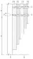
도 1a는 본 발명의 일 실시예들에 따른 반도체 소자의 평면도이다. 도 1b는 본 발명의 일 실시예들에 따른 반도체 소자의 단면도로서, 도 1a의 I-I'선에 대응하는 단면을 나타낸다. 이하, 도 1a 및 도 1b를 참조하여 본 발명의 일 실시예들에 따른 반도체 소자를 설명한다.1A is a plan view of a semiconductor device according to example embodiments. FIG. 1B is a cross-sectional view of a semiconductor device according to an exemplary embodiment of the present invention, and is a cross-sectional view corresponding to line I-I' of FIG. 1A. Hereinafter, a semiconductor device according to embodiments of the present invention will be described with reference to FIGS. 1A and 1B .
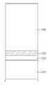
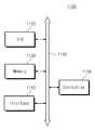
도 1a 및 도 1b를 참조하면, 본 발명의 일 실시예들에 따른 콘택 플러그(160)를 포함하는 반도체 소자(100)는 기판(110), 하부 절연막(120), 도전성 패턴(130), 매립 절연막(140), 배리어 막(150), 및 콘택 플러그(160)를 포함할 수 있다.1A and 1B , a
기판(110)은 반도체 기판일 수 있다. 반도체 기판은, 예를 들어, 단결정 실리콘막, SOI(silicon on insulator), 실리콘 게르마늄(SiGe)막 상에 형성된 실리콘 막, 절연막 상에 형성된 실리콘 단결정막, 및 절연막 상에 형성된 폴리실리콘막 중에서 선택된 적어도 하나를 포함할 수 있다.The
하부 절연막(120)은 기판(110) 상에 배치될 수 있다. 하부 절연막(120)은 실리콘 산화막 및/또는 실리콘 질화막을 포함할 수 있다.The lower
도전성 패턴(130)은 하부 절연막(120) 상에 배치될 수 있다. 도전성 패턴(130)은 도전성 패턴(130)의 상면에서 하면으로 연장되는 개구부(130a)를 가질 수 있다. 개구부(130a)의 평면적 단면은 원형일 수 있다. 도전성 패턴(130)은 도핑된 폴리실리콘, 금속(예를 들면, 텅스텐, 구리 또는 알루미늄), 도전성 금속질화물(예를 들면, 질화티타늄 또는 질화탄탈늄) 또는 전이 금속(예를 들면, 티타늄 또는 탄탈늄) 중에서 선택된 적어도 하나를 포함할 수 있다.The
매립 절연막(140)은 도전성 패턴(130)을 덮을 수 있다. 다만, 매립 절연막(140)은 개구부(130a)를 채우지 않을 수 있다. 매립 절연막(140)은 실리콘 산화막 및/또는 실리콘 질화막을 포함할 수 있다.The buried insulating
콘택 플러그(160)은 콘택 플레이트(161) 및 콘택 바디(162)를 포함할 수 있다. 콘택 플레이트(161)은 도전성 패턴(130)의 개구부(130a) 내에 삽입되어 도전성 패턴(130)과 전기적으로 연결될 수 있다. 콘택 플레이트(161)는 원판(circular plate) 구조를 가질 수 있으며, 개구부(130a)를 통하여 도전성 패턴(130)을 관통할 수 있다. 콘택 바디(162)의 하면은 콘택 플레이트(161)의 상면과 접할 수 있다. 콘택 플레이트(161)의 상면의 너비(W1)은 콘택 바디(162)의 하면의 너비(W2)보다 클 수 있다. 다시 말해, 콘택 플레이트(161)의 상면의 넓이는 콘택 바디(162)의 하면의 넓이보다 클 수 있다. 콘택 바디(162)는 콘택 플레이트(161)의 상면으로부터 수직하게 연장되어 매립 절연막(140)을 관통할 수 있다. 콘택 플레이트(161)와 콘택 바디(162)는 동일한 물질을 포함할 수 있다. 예를 들어, 콘택 플레이트(161) 및 콘택 바디(162)는 금속(예를 들면, 텅스텐, 구리 또는 알루미늄), 도전성 금속질화물(예를 들면, 질화티타늄 또는 질화탄탈늄) 또는 전이 금속(예를 들면, 티타늄 또는 탄탈늄) 중에서 선택된 적어도 하나를 포함할 수 있다.The
배리어 막(150)은 콘택 플레이트(161)의 표면 및 콘택 바디(162)의 측면을 컨포멀하게 덮을 수 있다. 다만, 콘택 플레이트(161)의 상면 중 콘택 바디(162)와 접하는 부분은 배리어 막(150)으로 덮이지 않을 수 있다. 이에 따라, 배리어 막(150)은 콘택 플러그(160)와 하부 절연막(120) 사이, 콘택 플러그(160)와 도전성 패턴(130) 사이, 및 콘택 플러그(160)와 매립 절연막(140) 사이에 개재될 수 있다. 콘택 플레이트(161)와 도전성 패턴(130)은 그들 사이에 개재된 배리어 막(150)을 통해 전기적으로 연결될 수 있다. 배리어 막(150)은 도전성 금속질화물(예를 들면, 질화티타늄 또는 질화탄탈늄)을 포함할 수 있다.The
본 발명에 따르면, 도전성 패턴(130)에 삽입된 콘택 플레이트(161)를 통해 도전성 패턴(130)과 콘택 플러그(160)가 전기적으로 연결된다. 이에 따라, 도전성 패턴(130)과 콘택 플러그(160)의 콘택 면적이 넓어져, 도전성 패턴(130)과 콘택 플러그(160) 사이의 콘택 저항이 작아질 수 있다.
According to the present invention, the
도 2a 내지 6a 및 도 3c는 본 발명의 일 실시예들에 따른 반도체 소자의 제조 방법을 나타내는 평면도들이다. 도 2b 내지 6b 및 도 3d는 본 발명의 일 실시예들에 따른 반도체 소자의 제조 방법을 나타내는 단면도들로서, 각각 도 2a 내지 6a 및 도 3c의 I-I'선에 대응한다. 이하, 도 2a 내지 6a, 도 3c, 도 2b 내지 6b, 및 도 3d를 참조하여 본 발명의 일 실시예들에 따른 반도체 소자의 제조 방법을 설명한다. 도 1a 및 도 1b를 참조하여 설명한 본 발명의 일 실시예들에 따른 반도체 소자와 동일한 구성에 대하여는 동일한 참조번호가 제공되고, 설명의 간소화를 위해 중복되는 설명은 생략될 수 있다.2A to 6A and 3C are plan views illustrating a method of manufacturing a semiconductor device according to example embodiments. 2B to 6B and 3D are cross-sectional views illustrating a method of manufacturing a semiconductor device according to an exemplary embodiment of the present invention, and correspond to the line II′ of FIGS. 2A to 6A and 3C , respectively. Hereinafter, a method of manufacturing a semiconductor device according to exemplary embodiments will be described with reference to FIGS. 2A to 6A, 3C, 2B to 6B, and 3D. The same reference numerals are provided to the same components as those of the semiconductor device according to the embodiments of the present invention described with reference to FIGS. 1A and 1B , and overlapping descriptions may be omitted for simplicity of description.
도 2a 및 도 2b를 참조하면, 기판(110) 상에 하부 절연막(120), 도전성 패턴(130), 및 매립 절연막(140)이 차례로 형성될 수 있다.2A and 2B , a lower insulating
기판(110)은 반도체 기판일 수 있다. 반도체 기판은, 예를 들어, 단결정 실리콘막, SOI(silicon on insulator), 실리콘 게르마늄(SiGe)막 상에 형성된 실리콘 막, 절연막 상에 형성된 실리콘 단결정막, 및 절연막 상에 형성된 폴리실리콘막 중에서 선택된 적어도 하나를 포함할 수 있다.The
하부 절연막(120)이 기판(110) 상에 형성될 수 있다. 하부 절연막(120)은, 예를 들어 실리콘 산화막 및/또는 실리콘 질화막을 포함할 수 있다. 하부 절연막(120)은, 예를 들어 열산화 공정에 의하여 형성될 수 있다.A lower insulating
하부 절연막(120) 상에 도전성 패턴(130)이 형성될 수 있다. 도전성 패턴(130)은, 예를 들어, 물리적 기상 증착법(physical vapor deposition: PVD) 또는 화학적 기상 증착법(physical vapor deposition CVD)을 통해 형성될 수 있다. 도전성 패턴(130)은 도핑된 폴리실리콘, 금속(예를 들면, 텅스텐, 구리 또는 알루미늄), 도전성 금속질화물(예를 들면, 질화티타늄 또는 질화탄탈늄) 또는 전이 금속(예를 들면, 티타늄 또는 탄탈늄) 중에서 선택된 적어도 하나를 포함할 수 있다.A
매립 절연막(140)이 도전성 패턴(130) 상에 형성될 수 있다. 이에 따라, 도전성 패턴(130)은 매립 절연막(140)에 의해 덮일 수 있다. 매립 절연막(140)은, 예를 들어, 화학적 기상 증착법(CVD)에 의하여 형성될 수 있다. 매립 절연막(140)은 실리콘 산화막 및/또는 실리콘 질화막을 포함할 수 있다.A filling insulating
도 3a 및 3b, 또는 도 3c 및 3d를 참조하면, 매립 절연막(140)을 관통하여 도전성 패턴(130)에 인접하는 콘택 홀(140a)을 형성할 수 있다. 콘택 홀(140a)은 매립 절연막(140) 상에 매립 절연막(140)의 일부를 노출하는 마스크(미도시)를 형성하고, 이를 식각 마스크로 이용하여 매립 절연막(140)을 식각함으로써 형성될 수 있다. 이 때, 식각은 도전성 패턴(130)보다 매립 절연막(140)에 대하여 더 빠른 식각 속도를 가지는 건식 식각(dry etching)에 의해 수행될 수 있다.3A and 3B or 3C and 3D , a
식각의 수행 시간을 조절함으로써 또는 공정 균일도에 따라 콘택 홀(140a)의 깊이가 달라질 수 있다. 식각의 수행 시간을 길게 하거나 또는 과도 식각(over-etch)됨에 따라 콘택 홀(140a)의 깊이는 커질 수 있다. 예를 들어, 도 3a 및 도 3b에 도시된 바와 같이, 콘택 홀(140a)에 의해 도전성 패턴(130)이 노출될 수 있다. 이 경우, 콘택 홀(140a)에 의해 노출된 도전성 패턴도 일부 식각될 수 있다. 이와 달리, 식각 시간을 짧게 하거나 미식각(un-etch)됨에 따라, 콘택홀(140a)의 깊이는 작아질 수 있다. 예를 들어, 도 3c 및 3d에 도시된 바와 같이, 콘택 홀(140a)에 의해 도전성 패턴(130)이 노출되지 않을 수 있다. 다시 말해, 콘택 홀(140a)과 도전성 패턴(130) 사이에 매립 절연막(140)의 잔존물(141)이 형성될 수 있다.The depth of the
도 4a 및 4b를 참조하면, 콘택 홀(140a)에 인접한 도전성 패턴(130)의 일부를 제거하여 도전성 패턴(130) 내에 개구부(130a)를 형성할 수 있다. 개구부(130a)는 하부 절연막(120) 및 매립 절연막(140)보다 도전성 패턴(130)에 대하여 더 빠른 식각 속도를 가지는 습식 식각을 수행함으로써 형성될 수 있다. 습식 식각에 의하여 매립 절연막(140)이 전혀 식각되지 않는 것은 아닐 수 있다. 따라서, 습식 식각에 의하여 콘택 홀(140a)의 내벽 부분의 매립 절연막(140)이 식각될 수 있으며, 이에 따라 콘택 홀(140a)의 너비가 커질 수 있다.4A and 4B , the
도 3a 및 3b에 도시된 실시예에서와 같이 콘택 홀(140a)에 의하여 도전성 패턴(130)의 일부가 노출된 경우, 노출된 부분을 중심으로 도전성 패턴(130)의 식각이 진행될 수 있다. 이에 따라, 개구부(130a)는 도전성 패턴(130)의 상면에서 하면으로 연장될 수 있으며, 개구부(130a)의 평면적 단면은 콘택 홀(140a)을 중심으로 하는 원의 형태로 형성될 수 있다. 또한, 개구부(130a)는 콘택 홀(140a)과 연결될 수 있다.As in the embodiment shown in FIGS. 3A and 3B , when a portion of the
도 3c 및 3d에 도시된 실시예에서와 같이 콘택 홀(140a)과 도전성 패턴(130) 사이에 매립 절연막(140)의 잔존물(도 3c 및 3d의 141 참조)이 형성된 경우, 습식 식각에 의하여 잔존물(도 3c 및 3d의 141 참조)이 제거될 수 있다. 잔존물(도 3c 및 3d의 141 참조)이 제거됨에 따라, 콘택 홀(140a)은 도전성 패턴(130)의 상면까지 연장될 수 있고, 콘택 홀(140a)를 통해 도전성 패턴(130)이 노출될 수 있다. 결국, 노출된 부분을 중심으로 도전성 패턴(130)의 식각이 진행될 수 있다. 이에 따라, 개구부(130a)는 도전성 패턴(130)의 상면에서 하면으로 연장될 수 있으며, 개구부(130a)의 평면적 단면은 콘택 홀(140a)을 중심으로 하는 원의 형태로 형성될 수 있다. 또한, 개구부(130a)는 콘택 홀(140a)과 연결될 수 있다.As in the embodiment shown in FIGS. 3C and 3D , when the residue of the buried insulating layer 140 (refer to 141 of FIGS. 3C and 3D ) is formed between the
습식 식각의 수행 시간을 조절함으로써, 개구부(130a)의 크기를 조절할 수 있다. 다시 말해, 습식 식각의 수행 시간을 길게 할수록 도전성 패턴(130)이 식각되는 정도가 커지기 때문에, 개구부(130a)의 크기는 커질 수 있다. 따라서, 습식 식각의 수행 시간을 충분히 길게 하면, 개구부(130a)의 너비(W3)는 콘택 홀(140a)의 너비(W4)보다 커질 수 있다.The size of the
도 5a 및 5b를 참조하면, 개구부(130a) 및 콘택 홀(140a)의 내벽을 컨포멀하게 덮는 배리어 막(150)을 형성할 수 있다. 배리어 막(150)은, 예를 들어, 화학적 기상 증착법(CVD)을 통해 형성될 수 있다. 배리어 막(150)은 도전성 금속질화물(예를 들면, 질화티타늄 또는 질화탄탈늄)을 포함할 수 있다.5A and 5B , the
도 6a 및 6b를 참조하면, 개구부(130a) 및 콘택 홀(140a)를 채우는 콘택 플러그(160)를 형성할 수 있다. 콘택 플러그(160)는 개구부(130a)를 채우는 부분인 콘택 플레이트(161)와 콘택 홀(140a)을 채우는 부분인 콘택 바디(162)를 포함할 수 있다. 개구부(130a)와 콘택 홀(140a)는 연결되므로, 콘택 바디(162)의 하면은 콘택 플레이트(161)의 상면과 접할 수 있다. 콘택 플레이트(161)은 배리어 막(150)을 통해 도전성 패턴(130)과 전기적으로 연결될 수 있다. 콘택 플레이트(161)는 개구부(130a)의 형태를 따라, 원판 구조를 가질 수 있으며, 도전성 패턴(130)을 관통하도록 형성될 수 있다. 개구부(130a)의 너비는 콘택 홀(140a)의 너비보다 클 수 있기 때문에, 콘택 플레이트(161)의 상면의 너비(W1)은 콘택 바디(162)의 하면의 너비(W2)보다 클 수 있다. 콘택 플러그(160)는 화학적 기상 증착법(CVD)을 통해 형성될 수 있다. 콘택 플레이트(161)와 콘택 바디(162)는 동일한 물질을 포함할 수 있다. 예를 들어, 콘택 플레이트(161) 및 콘택 바디(162)는 금속(예를 들면, 텅스텐, 구리 또는 알루미늄), 도전성 금속질화물(예를 들면, 질화티타늄 또는 질화탄탈늄) 또는 전이 금속(예를 들면, 티타늄 또는 탄탈늄) 중에서 선택된 적어도 하나를 포함할 수 있다.6A and 6B , a
본 발명에 따르면, 콘택 홀(도 3c 및 3d의 140a 참조)의 깊이가 충분하지 않아, 콘택 홀(140a)과 도전성 패턴(130) 사이에 잔존물(도 3c 및 3d의 141 참조)이 형성된다 하더라도, 습식 식각에 의해 잔존물(도 3c 및 3d의 141 참조)이 제거될 수 있다. 따라서, 도전성 패턴(130)과 안정적으로 접촉하는 콘택 플러그(160)가 형성될 수 있다.According to the present invention, even if the depth of the contact hole (see 140a in FIGS. 3C and 3D) is not sufficient, a residue (refer to 141 in FIGS. 3C and 3D) is formed between the
또한, 본 발명에 따르면, 도전성 패턴(130)에 삽입된 콘택 플레이트(161)를 통해 도전성 패턴(130)과 콘택 플러그(160)가 전기적으로 연결된다. 이에 따라, 도전성 패턴(130)과 콘택 플러그(160)의 콘택 면적이 넓어져, 도전성 패턴(130)과 콘택 플러그(160) 사이의 콘택 저항이 작아질 수 있다.
Also, according to the present invention, the
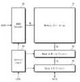
도 7은 본 발명의 실시예들에 따른 메모리 장치를 나타내는 블록도이다. 도 7을 참조하면, 본 발명의 실시예들에 따른 반도체 장치는 메모리 셀 어레이(10), 어드레스 디코더(20), 읽기/쓰기 회로(30), 데이터 입출력 회로(40), 및 제어 로직(50)을 포함할 수 있다.7 is a block diagram illustrating a memory device according to embodiments of the present invention. Referring to FIG. 7 , a semiconductor device according to example embodiments includes a
메모리 셀 어레이(10)는 복수 개의 워드 라인들(WL)을 통해 어드레스 디코더(20)에 연결되고, 비트 라인들(BL)을 통해 읽기 및 쓰기 회로(30)에 연결될 수 있다. 메모리 셀 어레이(10)는 복수 개의 메모리 셀들을 포함한다. 예를 들어, 메모리 셀 어레이(10)는 셀 당 하나 또는 그 이상의 비트를 저장할 수 있도록 구성된다.The
어드레스 디코더(20)는 워드 라인들(WL)을 통해 메모리 셀 어레이(10)에 연결될 수 있다. 어드레스 디코더(20)는 제어 로직(50)의 제어에 응답하여 동작하도록 구성된다. 어드레스 디코더(20)는 외부로부터 어드레스(ADDR)를 수신할 수 있다. 어드레스 디코더(20)는 수신된 어드레스(ADDR) 중 행 어드레스를 디코딩하여, 복수 개의 워드 라인들(WL) 중 대응하는 워드 라인을 선택한다. 또한, 어드레스 디코더(20)는 수신된 어드레스(ADDR) 중 열 어드레스를 디코딩하고, 디코딩된 열 어드레스를 읽기/쓰기 회로(30)에 전달한다. 예를 들어, 어드레스 디코더(20)는 행 디코더, 열 디코더, 어드레스 버퍼 등과 같이 잘 알려진 구성 요소들을 포함할 수 있다.The
읽기/쓰기 회로(30)는 비트 라인들(BL)을 통해 메모리 셀 어레이(10)에 연결되고, 데이터 라인들(D/L)을 통해 데이터 입출력 회로(40)에 연결될 수 있다. 읽기/쓰기 회로(30)는 제어 로직(50)의 제어에 응답하여 동작할 수 있다. 읽기/쓰기 회로(30)는 어드레스 디코더(20)로부터 디코딩된 열 어드레스를 수신하도록 구성된다. 디코딩된 열 어드레스를 이용하여, 읽기/쓰기 회로(30)는 비트 라인(BL)을 선택한다. 예를 들어, 읽기/쓰기 회로(30)는 데이터 입출력 회로(40)로부터 데이터를 수신하고, 수신된 데이터를 메모리 셀 어레이(10)에 기입한다. 읽기/쓰기 회로(30)는 메모리 셀 어레이(10)로부터 데이터를 읽고, 읽어진 데이터를 데이터 입출력 회로(40)에 전달한다. 읽기/쓰기 회로(30)는 메모리 셀 어레이(10)의 제1 저장 영역으로부터 데이터를 읽고, 읽어진 데이터를 메모리 셀 어레이(10)의 제2 저장 영역에 기입한다. 예를 들면, 읽기/쓰기 회로(30)는 카피-백(copy-back) 동작을 수행하도록 구성될 수 있다.The read/
읽기/쓰기 회로(30)는 페이지 버퍼(또는 페이지 레지스터) 및 열 선택 회로를 포함하는 구성 요소들을 포함할 수 있다. 다른 예로서, 읽기/쓰기 회로(30)는 감지 증폭기, 쓰기 드라이버, 및 열 선택 회로를 포함하는 구성 요소들을 포함할 수 있다.The read/
데이터 입출력 회로(40)는 데이터 라인들(DL)을 통해 읽기/쓰기 회로(30)에 연결될 수 있다. 데이터 입출력 회로(40)는 제어 로직(50)의 제어에 응답하여 동작한다. 데이터 입출력 회로(40)는 외부와 데이터(DATA)를 교환하도록 구성된다. 데이터 입출력 회로(40)는 외부로부터 전달되는 데이터(DATA)를 데이터 라인들(DL)을 통해 읽기/쓰기 회로(30)에 전달하도록 구성된다. 데이터 입출력 회로(40)는 읽기 및 쓰기 회로로부터 데이터 라인들(DL)을 통해 전달되는 데이터(DATA)를 외부로 출력하도록 구성된다. 예를 들어, 데이터 입출력 회로(40)는 데이터 버퍼 등과 같은 구성 요소를 포함할 수 있다.The data input/
제어 로직(50)은 어드레스 디코더(20), 읽기/쓰기 회로(30), 및 데이터 입출력 회로(40)에 연결될 수 있다. 제어 로직(50)은 반도체 장치의 동작을 제어하도록 구성된다. 제어 로직(50)은 외부로부터 전달되는 제어 신호(CTRL)에 응답하여 동작할 수 있다.
The
도 8은 도 7의 메모리 셀 어레이(10)의 예를 나타내는 블록도이다. 도 8을 참조하면, 메모리 셀 어레이(10)는 복수 개의 메모리 블록들(BLK1~BLKn)을 포함할 수 있다. 각 메모리 블록은 3차원 구조(또는 수직 구조)를 가질 수 있다. 예를 들면, 각 메모리 블록은 서로 교차하는 제 1 내지 제 3 방향들(D1, D2, D3)로 연장된 구조물들을 포함할 수 있다. 예를 들면, 각 메모리 블록은 제 3 방향(D3)으로 연장된 복수 개의 셀 스트링들을 포함한다.
8 is a block diagram illustrating an example of the
도 9는 본 발명의 개념에 의한 실시예들에 따른 것으로, 도 8의 메모리 블록의 셀 어레이(10)를 나타내는 간략 회로도이다. 도 9를 참조하면, 본 실시예에 따른 반도체 장치는 공통 소오스 라인(CSL), 비트라인들(BL), 및 공통 소오스 라인(CSL)과 비트라인들(BL) 사이에 배치되는 복수개의 셀 스트링들(CSTR)을 포함할 수 있다. 복수개의 셀 스트링들(CSTR)이 비트라인들(BL) 각각에 병렬로 연결된다.9 is a simplified circuit diagram illustrating the
셀 스트링들(CSTR) 각각은 공통 소오스 라인(CSL)에 접속하는 접지 선택 트랜지스터(GST), 비트라인들(BL) 각각에 접속하는 스트링 선택 트랜지스터(SST), 및 선택 트랜지스터들(GST, SST) 사이의 복수개의 메모리 셀 트랜지스터들(MCT)을 포함할 수 있다. 접지 선택 트랜지스터(GST), 스트링 선택 트랜지스터(SST), 및 메모리 셀 트랜지스터들(MCT)은 직렬로 연결될 수 있다. 접지 선택 라인(GSL), 복수개의 워드라인들(WL1 ~ WLn), 및 스트링 선택 라인(SSL)은 접지 선택 트랜지스터(GST), 메모리 셀 트랜지스터들(MCT), 및 스트링 선택 트랜지스터(SST)의 게이트 전극들에 각각 대응될 수 있다.
Each of the cell strings CSTR includes a ground select transistor GST connected to the common source line CSL, a string select transistor SST connected to each of the bit lines BL, and select transistors GST and SST. It may include a plurality of memory cell transistors MCT therebetween. The ground select transistor GST, the string select transistor SST, and the memory cell transistors MCT may be connected in series. The ground select line GSL, the plurality of word lines WL1 to WLn, and the string select line SSL are gates of the ground select transistor GST, the memory cell transistors MCT, and the string select transistor SST. Each of the electrodes may correspond to each other.
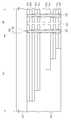
도 10a는 본 발명의 다른 실시예들에 따른 반도체 소자의 평면도이다. 도 10b는 도 10a의 I-I'선에 따른 단면도이다. 이하, 도 10a 및 도 10b를 참조하여, 본 발명의 다른 실시예에 따른 반도체 소자를 설명한다.10A is a plan view of a semiconductor device according to another exemplary embodiment of the present invention. 10B is a cross-sectional view taken along line I-I' of FIG. 10A. Hereinafter, a semiconductor device according to another exemplary embodiment of the present invention will be described with reference to FIGS. 10A and 10B .
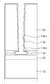
도 10a 및 10b를 참조하면, 본 발명의 다른 실시예에 따른 반도체 소자(200)는 기판(210), 적층 구조체들(ST), 매립 절연막(240), 배리어 막들(250), 콘택 플러그들(260), 및 수직 채널 구조체들(VCS)을 포함할 수 있다.10A and 10B , a
기판(210)은 소자 영역(DR) 및 연결 영역(CR)을 포함할 수 있다. 기판(210)은 제 1 도전형, 예를 들면 P형을 갖는 반도체 기판일 수 있다. 반도체 기판은 단결정 실리콘막, SOI(silicon on insulator), 실리콘 게르마늄(SiGe)막 상에 형성된 실리콘 막, 절연막 상에 형성된 실리콘 단결정막, 및 절연막 상에 형성된 폴리실리콘막을 구비하는 그룹에서 선택되는 적어도 하나를 포함할 수 있다.The
적층 구조체들(ST)은 기판(210) 상에 교대로 적층된 복수개의 절연막들(220) 및 전극들(230)을 포함할 수 있다. 적층 구조체들(ST)은 제 1 방향(D1)으로 연장될 수 있다. 각각의 전극들(230)은 게이트부(GP), 콘택부(CP), 및 게이트부(GP)와 콘택부(CP)를 연결하는 연장부(EP)를 가질 수 있다. 게이트부(GP)는 소자 영역(DR) 상에 제공되고, 연장부(EP) 및 콘택부(CP)는 연결 영역(CR) 상에 제공될 수 있다. 전극들(230)은 연결 영역(CR)에서 계단식 구조(stepwise structure)를 가질 수 있다. 즉, 기판(210)에서 먼 전극들(230)일수록 일 방향(D1)으로의 길이가 짧을 수 있다. 다시 말해, 기판(210)에서 먼 전극들(230)일수록 연장부(EP)가 짧을 수 있다. 이에 따라, 각 전극들(230)의 콘택부(CP)가 노출될 수 있다. 각각의 전극들(230)의 콘택부(CP)는 전극들(230)의 상면에서 하면으로 연장되는 개구부(230a)를 가질 수 있다. 개구부(230a)의 평면적 단면은 원형일 수 있다(도 1a 및 도 1b 참조). 전극(230)은 도핑된 폴리실리콘, 금속(예를 들면, 텅스텐, 구리 또는 알루미늄), 도전성 금속질화물(예를 들면, 질화티타늄 또는 질화탄탈늄) 또는 전이 금속(예를 들면, 티타늄 또는 탄탈늄) 중에서 선택된 적어도 하나를 포함할 수 있다. 절연막들(220)은 실리콘 산화막 및/또는 실리콘 질화막을 포함할 수 있다.The stacked structures ST may include a plurality of insulating
매립 절연막(240)은 전극들(230)의 단부들을 덮을 수 있다. 다만, 매립 절연막(240)은 개구부(230a)를 채우지 않을 수 있다. 매립 절연막(240)은 실리콘 산화막 및/또는 실리콘 질화막을 포함할 수 있다.The filling insulating
콘택 플러그들(260) 각각은 콘택 플레이트(261)과 콘택 바디(262)를 포함할 수 있다. 콘택 플레이트(261)은 각각의 전극들(230)의 개구부(230a) 내에 삽입되어 각각의 전극들(230)과 전기적으로 연결될 수 있다. 콘택 플레이트(261)는 원판(circular plate) 구조를 가질 수 있으며, 개구부(230a)를 따라 대응하는 전극(230)을 관통할 수 있다. 콘택 바디(262)의 하면은 콘택 플레이트(261)의 상면과 접할 수 있다. 콘택 플레이트(261)의 상면의 너비(W1)은 콘택 바디(262)의 하면의 너비(W2)보다 클 수 있다. 다시 말해, 콘택 플레이트(261)의 상면의 넓이는 콘택 바디(262)의 하면의 넓이보다 클 수 있다. 또한, 최상부 전극(230)의 콘택 플레이트(261)의 너비(W1a)는 최하부 전극(230)의 콘택 플레이트(261)의 너비(W1b)보다 클 수 있다. 콘택 바디(262)는 콘택 플레이트(261)의 상면으로부터 수직하게 연장되어 매립 절연막(240)을 관통할 수 있다. 콘택 플레이트(261)와 콘택 바디(262)는 동일한 물질을 포함할 수 있다. 예를 들어, 콘택 플레이트(261) 및 콘택 바디(262)는 금속(예를 들면, 텅스텐, 구리 또는 알루미늄), 도전성 금속질화물(예를 들면, 질화티타늄 또는 질화탄탈늄) 또는 전이 금속(예를 들면, 티타늄 또는 탄탈늄) 중에서 선택된 적어도 하나를 포함할 수 있다. 제 1 패드들(PAD1)이 매립 절연막(240) 상에 제공되어 콘택 플러그들(260)에 접속될 수 있다.Each of the contact plugs 260 may include a
배리어 막들(250)은 각각의 콘택 플레이트(261)의 표면 및 콘택 바디(262)의 측면을 컨포멀하게 덮을 수 있다. 다만, 콘택 플레이트(261)의 상면 중 콘택 바디(262)와 접하는 부분은 배리어 막(250)으로 덮이지 않을 수 있다. 이에 따라, 배리어 막들(250)은 콘택 플러그(260)와 절연막들(220) 사이, 콘택 플러그(260)와 전극들(230) 사이, 및 콘택 플러그(260)와 매립 절연막(240) 사이에 개재될 수 있다. 콘택 플레이트(261)와 이에 대응하는 전극(230)은 그들 사이에 개재된 배리어 막(250)을 통해 전기적으로 연결될 수 있다. 배리어 막(250)은 도전성 금속질화물(예를 들면, 질화티타늄 또는 질화탄탈늄)을 포함할 수 있다.The barrier layers 250 may conformally cover a surface of each
수직 채널 구조체들(VCS)은 소자 영역(DR) 상에서 적층 구조체들(ST)을 관통할 수 있다. 다시 말해, 수직 채널 구조체들(VCS)은 절연막들(220) 및 전극들(230)의 게이트부(GP)를 관통할 수 있다. 일 실시예에 따르면, 수직 채널 구조체들(VCS)은 기판(210)에 연결될 수 있다. 수직 채널 구조체들(VCS)은 평면적 관점에서 일 방향으로 지그재그 형태로 배열될 수 있다. 이와 달리, 수직 채널 구조체들(VCS)은 평면적 관점에서 일 방향으로 배열될 수 있다. 각각의 수직 채널 구조체들(VCS)은 활성 기둥(AP) 및 활성 기둥(AP)의 측벽에 배치되는 데이터 저장막(DS)을 포함할 수 있다.The vertical channel structures VCS may pass through the stack structures ST on the device region DR. In other words, the vertical channel structures VCS may pass through the insulating
일 실시예에 따르면, 적층 구조체들(ST) 사이의 반도체 기판(210) 내에 공통 소오스 영역들(CSR)이 형성될 수 있다. 공통 소오스 영역들(CSR)은 제 1 방향(D1)으로 나란히 연장될 수 있다. 적층 구조체들(ST) 및 공통 소오스 영역들(CSR)은 제 2 방향(D2)으로 교대로 그리고 반복적으로 배열될 수 있다. 공통 소오스 영역들(CSR)은 기판(210) 내에 제 2 도전형의 불순물을 도핑하여 형성될 수 있다. 즉, 공통 소오스 영역들(CSR)은 기판(210)과 반대의 도전형을 가질 수 있다.According to an embodiment, common source regions CSR may be formed in the
일 실시예에 따르면, 서로 인접하는 적층 구조체들(ST) 사이에 공통 소스 구조체(CSS)가 배치될 수 있다. 공통 소스 구조체(CSS)는 적층 구조체들(ST)의 측벽들을 덮는 측벽 절연 스페이서(SP)와, 측벽 절연 스페이서(SP)를 관통하여 공통 소오스 영역(CSR)과 접속되는 공통 소스 플러그(CSPLG)를 포함할 수 있다. 측벽 절연 스페이서(SP)는 실리콘 산화물, 실리콘 질화물, 실리콘 산질화물 또는 낮은 유전율을 가지는 low-k 물질로 형성될 수 있다 공통 소스 플러그(CSPLG)는 금속(예를 들어, 텅스텐, 구리 또는 알루미늄 등), 도전성 금속질화물(예를 들어, 질화티타늄 또는 질화탄탈늄 등) 및 전이 금속(예를 들어, 티타늄 또는 탄탈늄 등) 등에서 선택된 적어도 하나를 포함할 수 있다. 공통 소스 라인(CSL)이 매립 절연막(240) 상에 제공되어 공통 소스 플러그(CSPLG)와 연결될 수 있다.According to an embodiment, the common source structure CSS may be disposed between the stacked structures ST adjacent to each other. The common source structure CSS includes a sidewall insulating spacer SP covering sidewalls of the stacked structures ST, and a common source plug CSPLG passing through the sidewall insulating spacer SP and connected to the common source region CSR. may include The sidewall insulating spacer SP may be formed of silicon oxide, silicon nitride, silicon oxynitride, or a low-k material having a low dielectric constant. , may include at least one selected from a conductive metal nitride (eg, titanium nitride or tantalum nitride, etc.) and a transition metal (eg, titanium or tantalum, etc.). The common source line CSL may be provided on the buried insulating
제 1 캐핑 절연막(270)이 적층 구조체들(ST) 및 매립 절연막(240)을 덮을 수 있다. 제 1 캐핑 절연막(270)은 제 1 패드들(PAD1) 및 공통 소스 라인(CSL)을 덮을 수 있다. 제 1 캐핑 절연막(270)은 실리콘 산화막 및/또는 실리콘 질화막을 포함할 수 있다.The first
제 2 캐핑 절연막(280)이 제 1 캐핑 절연막(270) 상에 제공될 수 있다. 제 2 캐핑 절연막(280)은 실리콘 산화막 및/또는 실리콘 질화막을 포함할 수 있다. 제 2 캐핑 절연막(280) 상에 적층 구조체들(ST)을 가로질러 제 2 방향(D2)으로 연장되는 비트 라인들(BL)이 제공될 수 있다. 비트 라인들(BL)은 제 1 캐핑 절연막(270)을 관통하는 제 2 패드들(PAD2) 및 제 2 캐핑 절연막을 관통하는 비트 라인 플러그들(BPLG)을 통해 수직 채널 구조체들(VCS)과 전기적으로 연결될 수 있다.
A second
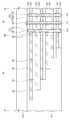
도 11a 내지 도 11l은 본 발명의 다른 실시예들에 따른 반도체 소자의 제조 방법에 관한 도면들로, 도 10a의 I-I'선에 대응되는 단면도들이다. 이하, 도 11a 내지 도 11l을 참조하여, 본 발명의 다른 실시예들에 따른 반도체 소자의 제조 방법을 설명한다. 도 10a 및 도 10b를 참조하여 설명한 본 발명의 다른 실시예들에 따른 반도체 소자와 동일한 구성에 대하여는 동일한 참조번호가 제공되고, 설명의 간소화를 위해 중복되는 설명은 생략될 수 있다.11A to 11L are views of a method of manufacturing a semiconductor device according to other embodiments of the present invention, and are cross-sectional views corresponding to line I-I' of FIG. 10A. Hereinafter, a method of manufacturing a semiconductor device according to other exemplary embodiments of the present invention will be described with reference to FIGS. 11A to 11L . The same reference numerals are provided to the same components as those of the semiconductor devices according to other embodiments of the present invention described with reference to FIGS. 10A and 10B , and overlapping descriptions may be omitted for simplicity of description.
도 10a 및 도 11a를 참조하면, 기판(210) 상에 절연막들(220) 및 희생막들(221)이 교대로 적층될 수 있다. 기판(210)은 소자 영역(DR) 및 연결 영역(CR)을 포함할 수 있다. 기판(210)은 제 1 도전형, 예를 들면 P형을 갖는 반도체 기판일 수 있다. 반도체 기판은 단결정 실리콘막, SOI(silicon on insulator), 실리콘 게르마늄(SiGe)막 상에 형성된 실리콘 막, 절연막 상에 형성된 실리콘 단결정막, 및 절연막 상에 형성된 폴리실리콘막을 구비하는 그룹에서 선택되는 적어도 하나를 포함할 수 있다. 희생막들(221)은 절연막들(220)에 대하여 습식 식각 특성이 다른 물질을 포함할 수 있다. 희생막들(221)은, 예를 들면 실리콘 질화막, 실리콘 산화질화막, 폴리실리콘막 또는 폴리실리콘 게르마늄막을 포함할 수 있다. 희생막들(221) 및 절연막들(220)은 예를 들어, 화학적 기상 증착(CVD) 방법에 의하여 형성될 수 있다.10A and 11A , insulating
도 10a 및 도 11b를 참조하면, 연결 영역(CR) 상의 절연막들(220) 및 희생막들(221)이 계단식 구조를 갖도록 식각될 수 있다. 즉, 기판(210)에서 먼 희생막들(221)일수록 일 방향(D1)으로 짧을 수 있다. 또한, 연결 영역(CR)에서 절연막들(220) 및 희생막들(221)의 단부들을 덮는 매립 절연막(240)이 형성될 수 있다. 매립 절연막(240)은 희생막들(221)에 대하여 습식 식각 특성이 다른 물질을 포함할 수 있다. 예를 들어 매립 절연막(240)은 절연막들(221)과 동일한 물질을 포함할 수 있다.10A and 11B , the insulating
도 10a 및 도 11c를 참조하면, 소자 영역(DR) 상에서 절연막들(220) 및 희생막들(221)을 관통하여 기판을 노출하는 수직 홀들(225)이 형성될 수 있다. 수직 홀들(225)을 형성하는 것은 이방성 식각 공정을 포함할 수 있다.Referring to FIGS. 10A and 11C ,
도 10a 및 도 11d를 참조하면, 수직 홀들(225)을 채우는 수직 채널 구조체들(VCS)이 형성될 수 있다. 각각의 수직 채널 구조체들(VCS)은 활성 기둥(AP) 및 활성 기둥(AP)의 측벽에 배치되는 데이터 저장막(DS)을 포함할 수 있다. 데이터 저장막(DS)는 수직 홀들의 내벽에 형성될 수 있으며, 예를 들어, 원자층 증착 방법(atomic layer deposition: ALD)으로 형성될 수 있다. 활성 기둥(AP)은 수직 홀들(225) 내의 데이터 저장막(DS) 사이에 형성될 수 있으며, 예를 들어, 화학적 기상 증착법(CVD) 또는 원자층 증착 방법(ALD)를 통해 형성될 수 있다.Referring to FIGS. 10A and 11D , vertical channel structures VCS filling the
도 10a 및 도 11e를 참조하면, 교대로 적층된 절연막들(220) 및 희생막들(221)을 패터닝하여 일방향(D1)으로 연장되는 분리 트렌치들(227)이 형성될 수 있다. 분리 트렌치들(227)에 의하여 기판(210)이 노출될 수 있고, 교대로 적층된 절연막들(220) 및 희생막들(221)은 복수개의 예비 적층 구조체들(PST)로 나눠질 수 있다.10A and 11E ,
도 10a 및 도 11f를 참조하면, 희생막들(221)을 제거하여 전극 영역들(229)을 형성할 수 있다. 전극 영역들(229)은 희생막들(221)이 제거된 영역에 해당되고, 수직 채널 구조체들(VCS), 절연막들(220), 및 매립 절연막(240)에 의해 한정된다. 희생막들(221)이 실리콘 질화막 또는 실리콘 산질화막을 포함하는 경우, 희생막(221)들의 제거 공정은 인산을 포함하는 식각 용액을 사용하여 수행될 수 있다.10A and 11F ,
도 10a 및 도 11g를 참조하면, 분리 트렌치들(227)을 통해 전극 영역들(229) 내에 도전막(미도시)이 형성될 수 있다. 도전막(미도시)은 도핑된 폴리실리콘, 금속(예를 들면, 텅스텐, 구리 또는 알루미늄), 도전성 금속질화물(예를 들면, 질화티타늄 또는 질화탄탈늄) 또는 전이 금속(예를 들면, 티타늄 또는 탄탈늄) 중에서 선택된 적어도 하나를 포함할 수 있다. 도전막(미도시)은 원자층 증착 방법(ALD)에 의하여 형성될 수 있다.10A and 11G , a conductive layer (not shown) may be formed in the
이어서, 전극 영역들(229)의 외부(즉, 분리 트렌치들(227))에 형성된 도전막이 제거된다. 이에 따라, 전극 영역들(229)의 내에 전극들(230)이 형성될 수 있다. 분리 트렌치들(227)에 형성된 도전막이 제거되어 반도체 기판(210)이 노출될 수 있다. 노출된 반도체 기판(210)에 제 2 도전형의 불순물 이온이 고농도로 제공되어 공통 소스 영역들(CSR)이 형성될 수 있다.Then, the conductive film formed on the outside of the electrode regions 229 (ie, the isolation trenches 227 ) is removed. Accordingly,
각각의 전극들(230)은 게이트부(GP), 콘택부(CP), 및 게이트부(GP)와 콘택부(CP)를 연결하는 연장부(EP)를 가질 수 있다. 게이트부(GP)는 소자 영역(DR) 상에 제공되고, 연장부(EP) 및 콘택부(CP)는 연결 영역(CR) 상에 제공될 수 있다. 상술한 희생막(도 11b의 221 참조)과 마찬가지로 전극들(230)은 연결 영역(CR)에서 계단식 구조를 가질 수 있다. 즉, 기판(210)에서 먼 전극들(230)일수록 일 방향(D1)으로의 길이가 짧을 수 있다. 다시 말해, 기판(210)에서 먼 전극들(230)일수록 연장부(EP)가 짧을 수 있다. 이에 따라, 각 전극들(230)의 콘택부(CP)는 다른 전극들(230)에 의하여 노출될 수 있다.Each of the
도 10a 및 도 11h를 참조하면, 분리 트렌치들(227)을 채우는 공통 소스 구조체들(CSS)이 형성될 수 있다. 공통 소스 구조체들(CSS)은 측벽 절연 스페이서(SP)와 공통 소스 플러그(CSPLG)를 포함할 수 있다. 측벽 절연 스페이서(SP)는 실리콘 산화막 또는 실리콘 질화막을 증착하고, 이를 이방성 식각하는 공정에 의하여 형성될 수 있다. 공통 소스 플러그(CSPLG)는 측벽 절연 스페이서(SP) 사이를 채우며 형성될 수 있으며, 예를 들어 화학적 기상 증착법(CVD)을 통해 형성될 수 있다. 공통 소스 플러그(CSPLG)는 금속(예를 들어, 텅스텐, 구리 또는 알루미늄 등), 도전성 금속질화물(예를 들어, 질화티타늄 또는 질화탄탈늄 등) 및 전이 금속(예를 들어, 티타늄 또는 탄탈늄 등) 등에서 선택된 적어도 하나를 포함할 수 있으며, 공통 소스 영역(CSR)과 전기적으로 연결될 수 있다.10A and 11H , common source structures CSS filling the
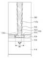
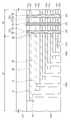
도 10a 및 도 11i를 참조하면, 절연막들(220) 및 매립 절연막(240)을 관통하여 각각의 전극들(230)의 콘택부(CP)에 인접하는 콘택 홀들(240a)이 형성될 수 있다. 콘택 홀들(240a)은 매립 절연막(240) 상에 매립 절연막(240)의 일부를 노출하는 마스크(미도시)를 형성하고, 이를 식각 마스크로 이용하여 매립 절연막(240)을 식각함으로써 형성될 수 있다. 이 때, 식각은 전극들(230)보다 절연막들(220) 및 매립 절연막(240)에 대하여 더 빠른 식각 속도를 가지는 건식 식각(dry etching)에 의해 수행될 수 있다.Referring to FIGS. 10A and 11I ,
식각이 수행됨에 따라, 기판(210)에서 먼 전극들(230)의 콘택부(CP)부터 차례대로 콘택 홀들(240a)에 의해 노출된다. 식각이 계속하여 수행됨에 따라, 노출된 전극들(230)의 콘택부(CP)에 리세스 영역(230b)이 형성될 수 있다. 리세스 영역(230b)의 깊이는 기판(210)에서 먼 전극들일수록 클 수 있다. 식각은 콘택 홀(240a)이 최하부 전극(230)에 인접할 때까지 수행될 수 있다. 식각의 수행 시간을 조정함으로써 최하부 전극(230)의 콘택부(CP)에 인접하는 콘택 홀(240a)의 깊이를 조절할 수 있다. 식각 시간을 충분히 길게 하면, 콘택 홀(240a)에 의해 최하부 전극(230)의 콘택부(CP)가 노출될 수 있다. 이러한 경우, 때때로 콘택 홀(240a)은 최상부 전극(230)을 관통할 수 있다. 때문에 식각 시간은 과도하게 충분히 할 수 없다. 이에 따라, 도 11i에 도시된 바와 같이, 최하부 전극(230)의 콘택부(CP)가 콘택 홀(240a)에 의해 노출되지 않을 수 있다. 다시 말해, 콘택 홀(240a)과 전극(230) 사이에 매립 절연막(240) 및/또는 절연막(220)의 잔존물(241)이 형성될 수 있다.As the etching is performed, the
도 10a 및 도 11j를 참조하면, 콘택 홀들(240a)에 인접한 전극들(230)의 일부를 제거하여 각각의 전극들(230) 내에 개구부(230a)를 형성할 수 있다. 개구부(230a)는 절연막들(220) 및 매립 절연막(240)보다 전극들(230)에 대하여 더 빠른 식각 속도를 가지는 습식 식각을 수행함으로써 형성될 수 있다. 습식 식각에 의하여 매립 절연막(240)이 전혀 식각되지 않는 것은 아닐 수 있다. 따라서, 습식 식각에 의하여 콘택 홀(240a)의 내벽 부분의 매립 절연막(240)이 식각될 수 있으며, 이에 따라 콘택 홀(240a)의 너비가 커질 수 있다.10A and 11J , a portion of the
콘택 홀(240a)에 의하여 전극(230)의 콘택부(CP)가 노출된 경우, 노출된 부분을 중심으로 전극(230)의 식각이 진행될 수 있다. 이에 따라, 개구부(230a)는 전극(230)의 상면에서 하면으로 연장될 수 있으며, 개구부(230a)의 평면적 단면은 콘택 홀(240a)을 중심으로 하는 원의 형태로 형성될 수 있다. 또한, 개구부(230a)는 콘택 홀(240a)과 연결될 수 있다.When the contact portion CP of the
도 11i에 도시된 최하부 전극(230)과 같이 콘택 홀(240a)과 전극(230) 사이에 잔존물(11i의 241 참조)이 형성된 경우, 습식 식각에 의하여 잔존물(11i의 241 참조)이 제거될 수 있다. 이러한 경우, 최하부 전극(230)의 실질적인 식각 수행 시간은 최상부 전극(230)보다 짧기 때문에, 최상부 전극(230)의 개구부(230a)의 너비(W3a)는 최하부 전극(230)의 개구부(230a)의 너비(W3b)보다 클 수 있다. 잔존물(11i의 241 참조)이 제거됨에 따라, 콘택 홀(240a)은 전극(230)의 상면까지 연장될 수 있고, 콘택 홀(240a)를 통해 전극(230)이 노출될 수 있다. 결국, 노출된 부분을 중심으로 전극(230)의 식각이 진행될 수 있다. 이에 따라, 개구부(230a)는 전극(230)의 상면에서 하면으로 연장될 수 있으며, 개구부(230a)의 평면적 단면은 콘택 홀(240a)을 중심으로 하는 원의 형태로 형성될 수 있다. 또한, 개구부(230a)는 콘택 홀(240a)과 연결될 수 있다.When a residue (refer to 241 of 11i) is formed between the
습식 식각의 수행 시간을 조절함으로써, 개구부(230a)의 크기를 조절할 수 있다. 다시 말해, 습식 식각의 수행 시간을 길게 할수록 전극(230)이 식각되는 정도가 커지기 때문에, 개구부(230a)의 크기는 커질 수 있다. 따라서, 습식 식각의 수행 시간을 충분히 길게 하면, 개구부(230a)의 너비(W3)는 콘택 홀(240a)의 너비(W4)보다 커질 수 있다.The size of the
도 10a 및 도 11k를 참조하면, 개구부(230a) 및 콘택 홀들(240a)의 내벽을 컨포멀하게 덮는 배리어 막들(250)이 형성될 수 있다. 배리어 막들(250)은, 예를 들어, 화학적 기상 증착법(CVD)을 통해 형성될 수 있다. 배리어 막들(250)은 도전성 금속질화물(예를 들면, 질화티타늄 또는 질화탄탈늄)을 포함할 수 있다.10A and 11K , barrier layers 250 may be formed to conformally cover inner walls of the
도 10a 및 도 11l을 참조하면, 개구부들(230a) 및 콘택 홀들(240a)을 채우는 콘택 플러그들(260)을 형성할 수 있다. 각각의 콘택 플러그들(260)은 개구부(230a)를 채우는 부분인 콘택 플레이트(261)와 콘택 홀(240a)을 채우는 부분인 콘택 바디(262)를 포함할 수 있다. 개구부(230a)와 콘택 홀(240a)은 연결되므로, 콘택 바디(262)의 하면은 콘택 플레이트(261)의 상면과 접할 수 있다. 콘택 플레이트(261)는 배리어 막(250)을 통해 대응하는 전극(230)과 전기적으로 연결될 수 있다. 콘택 플레이트(261)는 개구부(230a)의 형태를 따라, 원판 구조를 가질 수 있으며, 대응하는 전극(230)을 관통하도록 형성될 수 있다. 개구부(230a)의 너비는 콘택 홀(240a)의 너비보다 클 수 있기 때문에, 콘택 플레이트(261)의 상면의 너비(W1)은 콘택 바디(262)의 하면의 너비(W2)보다 클 수 있다. 콘택 플러그는 화학적 기상 증착법(CVD)을 통해 형성될 수 있다. 콘택 플레이트(261)와 콘택 바디(262)는 동일한 물질을 포함할 수 있다. 예를 들어, 콘택 플레이트(261) 및 콘택 바디(262)는 금속(예를 들면, 텅스텐, 구리 또는 알루미늄), 도전성 금속질화물(예를 들면, 질화티타늄 또는 질화탄탈늄) 또는 전이 금속(예를 들면, 티타늄 또는 탄탈늄) 중에서 선택된 적어도 하나를 포함할 수 있다.10A and 11L , contact plugs 260 may be formed to fill the
본 발명에 따르면, 콘택 홀들(240a)을 위한 식각 수행 시간이 충분하지 않거나 공정 균일도에 따라서 콘택 홀들(240a)과 전극들(230)(특히, 최하부 전극) 사이에 잔존물(도 11i의 241 참조)이 형성된다 하더라도, 습식 식각에 의해 잔존물(도 11i의 241 참조)이 제거될 수 있다. 따라서, 전극들(230)과 안정적으로 접촉하는 콘택 플러그들(260)이 형성될 수 있다.According to the present invention, a residue between the contact holes 240a and the electrodes 230 (particularly, the lowermost electrode) depending on the process uniformity or insufficient etching time for the contact holes 240a (refer to 241 of FIG. 11I ) Even if this is formed, the residue (refer to 241 of FIG. 11I ) may be removed by wet etching. Accordingly, contact plugs 260 stably contacting the
나아가, 콘택 홀들(240a)의 형성 시, 최하부 전극(230)의 노출을 위해 건식 식각의 수행 시간을 무리하게 늘릴 경우, 최상부 전극(230)이 뚫려 전극 간 단락 불량이 발생할 위험이 있다. 본 발명에 따르면, 최하부 전극(230)의 노출을 위해 건식 식각의 수행 시간을 무리하게 늘릴 필요가 없으므로, 이러한 전극 뚫림에 의한 전극 단락을 억제할 수 있다.Furthermore, when forming the
도 10a 및 도 10b를 다시 참조하면, 매립 절연막(240) 상에, 공통 소스 플러그(CSPLG)에 접속되는 공통 소스 라인(CSL) 및 콘택 플러그들(260)에 접속되는 제 1 패드들(PAD1)이 형성될 수 있다.Referring back to FIGS. 10A and 10B , on the buried insulating
이어서, 공통 소스 라인(CSL) 및 제 1 패드들(PAD1)을 덮는 제 1 캐핑 절연막(270)이 형성될 수 있다. 제 1 캐핑 절연막(270)은 실리콘 산화막 및/또는 실리콘 질화막을 포함할 수 있다. 제 1 캐핑 절연막(270)을 관통하여 활성 기둥(AP)과 전기적으로 연결되는 제 2 패드들(PAD2)이 형성될 수 있다.Subsequently, a first
그 후, 제 1 캐핑 절연막(270)을 덮는 제 2 캐핑 절연막(280)이 형성될 수 있다. 또한, 제 2 캐핑 절연막(280)을 관통하여 제 2 패드들(PAD2)과 전기적으로 연결되는 비트 라인 플러그들(BPLG)이 형성될 수 있다. 비트 라인들(BL)이 비트 라인 플러그들(BPLG) 상에 형성되어 비트 라인 플러그들(BPLG)을 제 2 방향(D2)으로 연결할 수 있다. 비트 라인들(BL) 및 비트 라인 플러그들(BPLG)은 금속(예를 들면, 텅스텐, 구리 또는 알루미늄), 도전성 금속질화물(예를 들면, 질화티타늄 또는 질화탄탈늄) 또는 전이 금속(예를 들면, 티타늄 또는 탄탈늄)에서 선택된 적어도 하나를 포함할 수 있다.
Thereafter, a second
도 12는 본 발명의 또 다른 실시예들에 따른 것으로, 도 8의 메모리 블록의 셀 어레이를 나타내는 간략 회로도이다.12 is a simplified circuit diagram illustrating a cell array of the memory block of FIG. 8 according to still another exemplary embodiment of the present invention.
도 12를 참조하면, 본 실시예들에 따른 반도체 소자의 셀 어레이는 공통 소스 라인(CSL), 복수 개의 비트 라인들(BL), 및 공통 소스 라인(CSL)과 비트 라인들(BL) 사이의 셀 스트링(CSTR)을 포함할 수 있다.Referring to FIG. 12 , the cell array of the semiconductor device according to the present embodiments includes a common source line CSL, a plurality of bit lines BL, and a common source line CSL and a cell array between the common source line CSL and the bit lines BL. It may include a cell string (CSTR).
공통 소스 라인(CSL)은 기판 상에 배치되는 도전성 박막일 수 있고, 비트 라인들(BL)은 기판 상에 배치되는 도전성 패턴들(일 예로, 금속 라인)일 수 있다.The common source line CSL may be a conductive thin film disposed on the substrate, and the bit lines BL may be conductive patterns (eg, a metal line) disposed on the substrate.
셀 스트링(CSTR)은 비트 라인들(BL)에 각각 연결된 복수 개의 상부 스트링들(CSTR1), 및 공통 소스 라인(CSL)에 연결된 단일의 하부 스트링(CSTR2)을 포함할 수 있다. 복수 개의 상부 스트링들(CSTR1)은 단일의 하부 스트링(CSTR2)에 공통적으로 연결될 수 있다. 상부 스트링들(CSTR1)의 각각은 스위칭 소자(SW)를 통해 하부 스트링(CSTR2)에 공통적으로 연결될 수 있다. 상부 스트링들(CSTR1)에 연결된 스위칭 소자들(SW)은 전기적으로 동일한 전압이 인가되도록 제어될 수 있다.The cell string CSTR may include a plurality of upper strings CSTR1 respectively connected to the bit lines BL, and a single lower string CSTR2 connected to the common source line CSL. The plurality of upper strings CSTR1 may be commonly connected to a single lower string CSTR2 . Each of the upper strings CSTR1 may be commonly connected to the lower string CSTR2 through the switching element SW. The switching elements SW connected to the upper strings CSTR1 may be controlled to electrically apply the same voltage.
상부 스트링들(CSTR1)의 각각은 비트 라인들(BL)의 각각에 접속하는 스트링 선택 트랜지스터(SST), 및 스트링 선택 트랜지스터(SST)와 스위칭 소자(SW) 사이에 배치되는 복수 개의 상부 메모리 셀 트랜지스터들(MCT1)을 포함할 수 있다. 스트링 선택 트랜지스터(SST) 및 상부 메모리 셀 트랜지스터들(MCT1)은 직렬로 연결될 수 있다. 하부 스트링(CSTR2)은 공통 소스 라인(CSL)에 접속하는 접지 선택 트랜지스터(GST), 및 접지 선택 트랜지스터(GST)와 스위칭 소자들(SW) 사이에 배치되는 복수 개의 하부 메모리 셀 트랜지스터들(MCT2)을 포함할 수 있다. 접지 선택 트랜지스터(GST) 및 하부 메모리 셀 트랜지스터들(MCT2)은 직렬로 연결될 수 있다.Each of the upper strings CSTR1 includes a string select transistor SST connected to each of the bit lines BL, and a plurality of upper memory cell transistors disposed between the string select transistor SST and the switching element SW. may include MCT1. The string select transistor SST and the upper memory cell transistors MCT1 may be connected in series. The lower string CSTR2 includes a ground select transistor GST connected to the common source line CSL, and a plurality of lower memory cell transistors MCT2 disposed between the ground select transistor GST and the switching elements SW. may include. The ground select transistor GST and the lower memory cell transistors MCT2 may be connected in series.
비트 라인들(BL)과 스위칭 소자들(SW) 사이에 배치되는 스트링 선택 라인(SSL) 및 상부 워드 라인들(WL1(0)-WL1(3))은, 스트링 선택 트랜지스터(SST) 및 상부 메모리 셀 트랜지스터들(MCT1)의 게이트 전극들로 각각 이용될 수 있다. 공통 소스 라인(CSL)과 스위칭 소자들(SW) 사이에 배치되는 접지 선택 라인(GSL) 및 하부 워드 라인들(WL2(0)-WL2(3))은, 접지 선택 트랜지스터(GST) 및 하부 메모리 셀 트랜지스터들(MCT2)의 게이트 전극들로 각각 이용될 수 있다. 상부 및 하부 메모리 셀 트랜지스터들(MCT1, MCT2)의 각각은 정보저장 요소를 포함할 수 있다.The string select line SSL and the upper word lines WL1 ( 0 ) - WL1 ( 3 ) disposed between the bit lines BL and the switching elements SW include the string select transistor SST and the upper memory. Each of the cell transistors MCT1 may be used as gate electrodes. The ground select line GSL and the lower word lines WL2( 0 ) - WL2( 3 ) disposed between the common source line CSL and the switching elements SW include the ground select transistor GST and the lower memory. Each of the cell transistors MCT2 may be used as gate electrodes. Each of the upper and lower memory cell transistors MCT1 and MCT2 may include an information storage element.
비트 라인들(BL)의 각각에 연결된 복수 개의 상부 스트링들(CSTR1)이 공통 소스 라인에 연결된 단일의 하부 스트링(CSTR2)에 공통적으로 연결될 수 있다. 이에 따라, 비트 라인들(BL)에 각각 접속하는 스트링 선택 트랜지스터들(SST)을 포함하는 상부 스트링들(CSTR1)은, 단일의 하부 스트링(CSTR2)에 포함된 접지 선택 트랜지스터(GST)를 공유할 수 있다. 즉, 서로 다른 비트 라인들에 연결되어 독립적으로 동작하는 상부 스트링들(CSTR1)이 단일의 하부 스트링(CSTR2)에 공통적으로 연결되어 접지 선택 트랜지스터(GST)를 공유하도록 구성됨에 따라, 고집적화에 최적화된 반도체 소자가 제공될 수 있다.
A plurality of upper strings CSTR1 connected to each of the bit lines BL may be commonly connected to a single lower string CSTR2 connected to a common source line. Accordingly, the upper strings CSTR1 including the string select transistors SST respectively connected to the bit lines BL share the ground select transistor GST included in the single lower string CSTR2. can That is, the upper strings CSTR1 that are connected to different bit lines and operate independently are commonly connected to a single lower string CSTR2 and are configured to share the ground select transistor GST, and thus optimized for high integration. A semiconductor device may be provided.
도 13은 본 발명의 또 다른 실시예들에 따른 반도체 소자의 단면도로서, 도 10a 및 10b를 참조하여 설명한 반도체 소자의 소자 영역(도 10a 및 10b의 DR 참조)에 대응되는 부분을 도시한 것이다. 이하, 도 13을 참조하여 본 발명의 또 다른 실시예에 따른 반도체 장치를 설명한다.13 is a cross-sectional view of a semiconductor device according to still another exemplary embodiment of the present invention, illustrating a portion corresponding to the device region (refer to DR of FIGS. 10A and 10B ) of the semiconductor device described with reference to FIGS. 10A and 10B . Hereinafter, a semiconductor device according to another embodiment of the present invention will be described with reference to FIG. 13 .
도 13을 참조하면, 본 발명의 또 다른 실시예들에 따른 반도체 장치(300)는 기판(310), 기판(310) 상의 비트 라인들(BL), 기판(310)과 비트 라인들(BL) 사이의 적층 구조체들(ST), 적층 구조체들(ST)과 비트 라인들(BL) 사이의 공통 소스 라인(CSL), 및 적층 구조체들(ST)을 관통하는 수직 채널 구조체들(VCS)을 포함할 수 있다. 적층 구조체들(ST)은 교대로 적층된 복수개의 절연막들(320) 및 전극들(330)을 포함할 수 있다. 각각의 수직 채널 구조체들(VCS)은 활성 기둥(AP), 데이터 저장막(DS), 및 충진 절연막(FI)을 포함할 수 있다. 활성 기둥(AP)은 비트 라인들(BL)과 공통 소스 라인(CSL)을 연결할 수 있다. 적층 구조체들(ST)과 비트 라인들(BL) 사이에, 이들 사이의 전기적 연결을 위한 비트 라인 플러그들(PLG) 및 패드(PAD)가 더 배치될 수 있다.Referring to FIG. 13 , a
적층 구조체들(ST)은 제 1 방향(D1)으로 연장될 수 있다. 적층 구조체들(ST)은 제 1 방향(D1)으로 연장되는 분리 트렌치들(327)에 의하여, 제 1 방향에 교차하는(예를 들어, 직교하는) 제 2 방향(D2)으로 서로 이격될 수 있다. 적층 구조체들(ST)은 교대로 적층된 복수개의 절연막들(320) 및 전극들(330)을 포함할 수 있다. 전극들(330)은 도핑된 실리콘, 금속(예를 들어, 텅스텐), 금속 질화물, 금속 실리사이드들 또는 이들의 조합을 포함할 수 있다. 절연막들(320)은 실리콘 산화막일 수 있다.The stacked structures ST may extend in the first direction D1 . The stacked structures ST may be spaced apart from each other in a second direction D2 crossing (eg, orthogonal to) the first direction by the
전극들(330)은 기판(310) 상에 차례로 수직적으로(제 3 방향, D3) 적층될 수 있다. 전극들(330)은 스트링 선택 라인(SSL), 워드 라인들(WL), 및 접지 선택 라인(GSL)을 포함할 수 있다. 스트링 선택 라인(SSL)은 워드 라인들(WL)과 비트 라인들(BL) 사이에 배치된다. 접지 선택 라인(GSL)은 워드 라인들(WL)과 공통 소스 라인(CSL) 사이에 배치된다. 워드 라인들(WL)은 기판(310) 상에 순차적으로 적층된다. 스트링 선택 라인(SSL) 및 접지 선택 라인(GSL)은 워드 라인들(WL) 상에 배치될 수 있다. 스트링 선택 라인(SSL)과 접지 선택 라인(GSL)은 분리 트렌치(327)에 의하여 제 2 방향(D2)으로 서로 이격될 수 있다. 워드 라인들(WL)은 기판(310)과 스트링 선택 라인(SSL) 사이에 배치되는 상부 워드 라인들(WL1), 및 기판(310)과 접지 선택 라인(GSL) 사이에 배치되는 하부 워드 라인들(WL2)을 포함할 수 있다. 상부 워드 라인들(WL1)과 하부 워드 라인들(WL2)은 분리 트렌치(327)에 의하여 제 2 방향(D2)으로 서로 이격될 수 있다.The
스트링 선택 라인(SSL)과 접지 선택 라인(GSL) 사이, 및 상부 워드 라인들(WL1)과 하부 워드 라인들(WL2) 사이에 소자 분리 패턴(DSP)이 제공될 수 있다. 소자 분리 패턴(DSP)은 제 1 방향(D1)으로 연장되는 라인 형태일 수 있다. 소자 분리 패턴(DSP)은 분리 트렌치(327)를 채우는 실리콘 산화막, 실리콘 질화막, 및/또는 실리콘 산질화막 중 적어도 하나를 포함할 수 있다.The device isolation pattern DSP may be provided between the string select line SSL and the ground select line GSL and between the upper word lines WL1 and the lower word lines WL2 . The device isolation pattern DSP may have a line shape extending in the first direction D1 . The device isolation pattern DSP may include at least one of a silicon oxide layer, a silicon nitride layer, and/or a silicon oxynitride layer filling the
복수개의 활성 기둥들(AP)은 적층 구조체(ST)를 관통할 수 있다. 활성 기둥들(AP)은 평면적 관점에서 제 1 방향(D1)을 따라 배열될 수 있다.The plurality of active pillars AP may pass through the stacked structure ST. The active pillars AP may be arranged along the first direction D1 in a plan view.
활성 기둥들(AP)의 각각은 적층 구조체들(ST)을 관통하는 수직 부분들(VP) 및 적층 구조체들(ST) 아래에서 수직 부분들(VP)을 연결하는 수평 부분(HP)을 포함할 수 있다. 수직 부분들(VP)은 적층 구조체(ST)를 관통하는 수직 홀들(325) 내에 제공될 수 있다. 수평 부분(HP)은 기판(310) 상부의 수평 리세스부(RC) 내에 제공될 수 있다. 수직 부분들(VP) 중의 하나는 공통 소스 라인(CSL)에 연결되고, 수직 부분들(VP) 중의 다른 하나는 비트 라인들(BL) 중의 어느 하나에 연결될 수 있다. 수평 부분(HP)은 기판(310)과 적층 구조체(ST) 사이에 제공되어 수직 부분들(VP)을 연결할 수 있다.Each of the active pillars AP may include vertical portions VP passing through the stacked structures ST and a horizontal portion HP connecting the vertical portions VP under the stacked structures ST. can The vertical portions VP may be provided in
보다 구체적으로, 활성 기둥들(AP)의 각각에 있어서, 수직 부분들(VP)은 상부 워드 라인들(WL1)과 스트링 선택 라인(SSL)을 관통하는 제 1 수직 부분(VP1), 및 하부 워드 라인들(WL2)과 접지 선택 라인(GSL)을 관통하는 제 2 수직 부분(VP2)을 포함할 수 있다. 제 1 수직 부분(VP1)은 비트 라인들(BL) 중 어느 하나에 연결되고, 제 2 수직 부분(VP2)은 공통 소스 라인(CSL)에 연결될 수 있다. 수평 부분(HP)은 상부 워드 라인들(WL1)의 아래에서 하부 워드 라인들(WL2)의 아래로 연장되어 제 1 수직 부분(VP1) 및 제 2 수직 부분(VP2)을 연결할 수 있다.More specifically, in each of the active pillars AP, the vertical portions VP include a first vertical portion VP1 passing through the upper word lines WL1 and the string selection line SSL, and a lower word. A second vertical portion VP2 passing through the lines WL2 and the ground selection line GSL may be included. The first vertical portion VP1 may be connected to any one of the bit lines BL, and the second vertical portion VP2 may be connected to the common source line CSL. The horizontal portion HP may extend below the lower word lines WL2 under the upper word lines WL1 to connect the first vertical portion VP1 and the second vertical portion VP2 .
활성 기둥들(AP)의 각각은 속이 빈 실린더 형(예를 들면, 마카로니(macaroni))으로, 내부 홀(IH)을 가질 수 있다. 활성 기둥들(AP)의 내부 홀들(IH)은 충진 절연막(FI)으로 채워질 수 있다. 충진 절연막(FI)은 실리콘 산화막으로 형성될 수 있다.Each of the active pillars AP may have a hollow cylindrical shape (eg, macaroni), and may have an inner hole IH. The inner holes IH of the active pillars AP may be filled with a filling insulating layer FI. The filling insulating layer FI may be formed of a silicon oxide layer.
활성 기둥들(AP)과 전극들(330)사이에 데이터 저장막(DS)이 제공될 수 있다. 게이트 절연막(GOX)이 활성 기둥들(AP)과 기판(310) 사이에 제공될 수 있다. 게이트 절연막(GOX)은 실리콘 산화막일 수 있다.A data storage layer DS may be provided between the active pillars AP and the
제 1 방향(D1)으로 연장된 적층 구조체들(ST)은 도 10a 및 10b를 참조하여 설명한 연결 영역(도 10a 및 10b의 CR 참조)과 실질적으로 동일한 구조를 갖는 연결 영역(미도시)을 형성할 수 있다. 제 1 방향(D1)으로 연장된 각각의 전극들(330)은 콘택부 및 소자 영역에서 연장되어 콘택부와 연결되는 연장부를 가질 수 있다. 전극들(330)은 연결 영역에서 계단식 구조를 가질 수 있으며, 이에 따라, 각 전극들(330)의 콘택부는 노출될 수 있다. 매립 절연막(미도시)이 연결 영역 상에 제공되어 전극들(330)의 단부를 덮을 수 있다. 각각의 전극들(330)의 콘택부는 전극들(330)의 상면에서 하면으로 연장되는 개구부(미도시)를 가질 수 있다. 개구부의 평면적 단면은 원형일 수 있다. 연결 영역 상에 콘택 플러그들(미도시)이 배치될 수 있다. 콘택 플러그들은 각각 콘택 플레이트과 콘택 바디를 포함할 수 있다. 콘택 플레이트는 각각의 전극들(330)의 개구부 내에 삽입되어 각각의 전극들(330)과 전기적으로 연결될 수 있다. 콘택 플레이트는 원판 구조를 가질 수 있으며, 개구부를 따라 대응하는 전극을 관통할 수 있다. 콘택 바디의 하면은 콘택 플레이트의 상면과 접할 수 있다. 콘택 플레이트의 상면의 너비은 콘택 바디의 하면의 너비보다 클 수 있다. 콘택 바디는 콘택 플레이트의 상면으로부터 수직하게 연장되어 매립 절연막을 관통할 수 있다. 배리어 막들(미도시)은 각각의 콘택 플레이트의 표면 및 콘택 바디의 측면을 컨포멀하게 덮을 수 있다.
The stacked structures ST extending in the first direction D1 form a connection region (not shown) having substantially the same structure as the connection region described with reference to FIGS. 10A and 10B (see CR of FIGS. 10A and 10B ). can do. Each of the
도 14는 본 발명의 개념에 의한 실시예들에 따라 형성된 메모리 장치를 포함하는 전자 시스템의 일 예를 나타내는 개략 블록도이다.14 is a schematic block diagram illustrating an example of an electronic system including a memory device formed according to embodiments according to the inventive concept.
도 14를 참조하면, 본 발명의 실시예들에 따른 전자 시스템(1100)은 컨트롤러(1110), 입출력 장치(1120, I/O), 기억 장치(1130, memory device), 인터페이스(1140) 및 버스(1150, bus)를 포함할 수 있다. 컨트롤러(1110), 입출력 장치(1120), 기억 장치(1130) 및/또는 인터페이스(1140)는 상기 버스(1150)를 통하여 서로 결합 될 수 있다. 버스(1150)는 데이터들이 이동되는 통로(path)에 해당한다. 기억 장치(1130, memory device)는 본 발명의 실시예들에 따른 메모리 장치를 포함할 수 있다.Referring to FIG. 14 , an
컨트롤러(1110)는 마이크로프로세서, 디지털 신호 프로세스, 마이크로 컨트롤러, 및 이들과 유사한 기능을 수행할 수 있는 논리 소자들 중에서 적어도 하나를 포함할 수 있다. 입출력 장치(1120)는 키패드(keypad), 키보드 및 디스플레이 장치 등을 포함할 수 있다. 기억 장치(1130)는 데이터 및/또는 명령어 등을 저장할 수 있다. 인터페이스(1140)는 통신 네트워크로 데이터를 전송하거나 통신 네트워크로부터 데이터를 수신하는 기능을 수행할 수 있다. 인터페이스(1140)는 유선 또는 무선 형태일 수 있다. 예컨대, 인터페이스(1140)는 안테나 또는 유무선 트랜시버 등을 포함할 수 있다. 도시하지 않았지만, 전자 시스템(1100)은 컨트롤러(1110)의 동작을 향상시키기 위한 동작 기억 소자로서, 고속의 디램 소자 및/또는 에스램 소자 등을 더 포함할 수도 있다.The
전자 시스템(1100)은 개인 휴대용 정보 단말기(PDA, personal digital assistant) 포터블 컴퓨터(portable computer), 웹 타블렛(web tablet), 무선 전화기(wireless phone), 모바일 폰(mobile phone), 디지털 뮤직 플레이어(digital music player), 메모리 카드(memory card), 또는 정보를 무선환경에서 송신 및/또는 수신할 수 있는 모든 전자 제품에 적용될 수 있다.
The
도 15는 본 발명의 개념에 의한 실시예들에 따라 형성된 메모리 장치를 구비하는 메모리 카드의 일 예를 나타내는 개략 블록도이다.15 is a schematic block diagram illustrating an example of a memory card having a memory device formed according to embodiments according to the inventive concept.
도 15를 참조하면, 메모리 카드(1200)는 기억 장치(1210)를 포함한다. 기억 장치(1210)는 전술한 실시예들에 개시된 메모리 장치를 포함할 수 있다. 또한, 기억 장치(1210)는 다른 형태의 반도체 메모리 장치(ex, 디램 장치 및/또는 에스램 장치 등)를 더 포함할 수 있다. 메모리 카드(1200)는 호스트(Host)와 기억 장치(1210) 간의 데이터 교환을 제어하는 메모리 컨트롤러(1220)를 포함할 수 있다.Referring to FIG. 15 , the
메모리 컨트롤러(1220)는 메모리 카드의 전반적인 동작을 제어하는 프로세싱 유닛(1222)을 포함할 수 있다. 또한, 메모리 컨트롤러(1220)는 프로세싱 유닛(1222)의 동작 메모리로써 사용되는 에스램(1221, SRAM)을 포함할 수 있다. 이에 더하여, 메모리 컨트롤러(1220)는 호스트 인터페이스(1223), 메모리 인터페이스(1225)를 더 포함할 수 있다. 호스트 인터페이스(1223)는 메모리 카드(1200)와 호스트(Host)간의 데이터 교환 프로토콜을 구비할 수 있다. 메모리 인터페이스(1225)는 메모리 컨트롤러(1220)와 기억 장치(1210)를 접속시킬 수 있다. 더 나아가서, 메모리 컨트롤러(1220)는 에러 정정 블록(1224, Ecc)를 더 포함할 수 있다. 에러 정정 블록(1224)은 기억 장치(1210)로부터 독출된 데이터의 에러를 검출 및 정정할 수 있다. 도시하지 않았지만, 메모리 카드(1200)는 호스트(Host)와의 인터페이싱을 위한 코드 데이터를 저장하는 롬 장치(ROM device)를 더 포함할 수도 있다. 메모리 카드(1200)는 휴대용 데이터 저장 카드로 사용될 수 있다. 이와는 달리, 메모리 카드(1200)는 컴퓨터시스템의 하드디스크를 대체할 수 있는 고상 디스트(SSD, Solid State Disk)로도 구현될 수 있다.
The
도 16은 본 발명의 개념에 의한 실시예들에 따라 형성된 메모리 장치를 장착한 정보 처리 시스템의 일 예를 나타내는 개략 블록도이다.16 is a schematic block diagram illustrating an example of an information processing system equipped with a memory device formed according to embodiments according to the inventive concept.
도 16을 참조하면, 모바일 기기나 데스크 톱 컴퓨터와 같은 정보 처리 시스템에 플래시 메모리 시스템(1310)이 장착된다. 플래시 메모리 시스템(1310)은 플래시 메모리(1311) 및 메모리 콘트롤러(1312)를 포함할 수 있다. 플래시 메모리(1311)는 본 발명의 개념에 의한 실시예들에 따른 메모리 장치를 포함할 수 있다. 정보 처리 시스템(1300)은 플래시 메모리 시스템(1310)과 각각 시스템 버스(1360)에 전기적으로 연결된 모뎀(1320), 중앙처리장치(1330), 램(1340), 유저 인터페이스(1350)를 포함한다. 플래시 메모리 시스템(1310)에는 중앙처리장치(1330)에 의해서 처리된 데이터 또는 외부에서 입력된 데이터가 저장된다. 여기서, 상술한 플래시 메모리 시스템(1310)이 반도체 디스크 장치(SSD)로 구성될 수 있으며, 이 경우 정보 처리 시스템(1300)은 대용량의 데이터를 플래시 메모리 시스템(1310)에 안정적으로 저장할 수 있다. 그리고 신뢰성의 증대에 따라, 플래시 메모리 시스템(1310)은 에러 정정에 소요되는 자원을 절감할 수 있어 고속의 데이터 교환 기능을 정보 처리 시스템(1300)에 제공할 것이다. 도시되지 않았지만, 정보 처리 시스템(1300)에는 응용 칩셋(Application Chipset), 카메라 이미지 프로세서(Camera Image Processor: CIS), 입출력 장치 등이 더 제공될 수 있음은 이 분야의 통상적인 지식을 습득한 자들에게 자명하다.
Referring to FIG. 16 , a
이상, 첨부된 도면을 참조하여 본 발명의 실시예를 설명하였지만, 본 발명이 속하는 기술분야에서 통상의 지식을 가진 자는 본 발명이 그 기술적 사상이나 필수적인 특징을 변경하지 않고서 다른 구체적인 형태로 실시될 수 있다는 것을 이해할 수 있을 것이다. 그러므로 이상에서 기술한 실시예에는 모든 면에서 예시적인 것이며 한정적이 아닌 것으로 이해해야만 한다.As mentioned above, although embodiments of the present invention have been described with reference to the accompanying drawings, those of ordinary skill in the art to which the present invention pertains can implement the present invention in other specific forms without changing its technical spirit or essential features. You will understand that there is Therefore, it should be understood that the embodiments described above are illustrative in all respects and not restrictive.
Claims (10)
Translated fromKorean상기 제1 및 제2 도전성 패턴들을 덮는 매립 절연막; 및
상기 제1 도전성 패턴 및 상기 제2 도전성 패턴에 각각 연결되는 제1 콘택 플러그 및 제2 콘택 플러그를 포함하되,
상기 제1 콘택 플러그는 상기 제1 도전성 패턴 내의 제1 콘택 플레이트, 및 상기 제1 콘택 플레이트의 상면과 접하며 상기 매립 절연막을 관통하는 제1 콘택 바디를 포함하고, 상기 제1 콘택 플레이트의 상기 상면의 너비는 상기 제1 콘택 바디의 하면의 너비보다 크고,
상기 제2 콘택 플러그는 상기 제2 도전성 패턴 내의 제2 콘택 플레이트, 및 상기 제2 콘택 플레이트의 상면과 접하며 상기 매립 절연막을 관통하는 제2 콘택 바디를 포함하고, 상기 제2 콘택 플레이트의 상기 상면의 너비는 상기 제2 콘택 바디의 하면의 너비보다 큰 반도체 소자.A first conductive pattern and a second conductive pattern stacked on a substrate, each of the first and second conductive patterns extends in a first direction, and a length of the second conductive pattern along the first direction is equal to the first a length smaller than a length of the conductive pattern in the first direction;
a buried insulating layer covering the first and second conductive patterns; and
a first contact plug and a second contact plug respectively connected to the first conductive pattern and the second conductive pattern;
The first contact plug includes a first contact plate in the first conductive pattern, and a first contact body in contact with a top surface of the first contact plate and penetrating the buried insulating layer, and The width is greater than the width of the lower surface of the first contact body,
The second contact plug includes a second contact plate in the second conductive pattern, and a second contact body in contact with a top surface of the second contact plate and penetrating the buried insulating layer, and A width of the semiconductor device is greater than a width of a lower surface of the second contact body.
상기 제1 콘택 플레이트는 원판(circular plate) 구조를 갖는 반도체 소자.The method of claim 1,
The first contact plate is a semiconductor device having a circular plate structure.
상기 제1 콘택 플레이트의 표면 및 상기 제1 콘택 바디의 측면을 컨포멀하게 덮는 제1 배리어 막을 더 포함하는 반도체 소자.The method of claim 1,
and a first barrier layer conformally covering a surface of the first contact plate and a side surface of the first contact body.
상기 제1 콘택 플레이트는 상기 제1 도전성 패턴을 관통하는 반도체 소자.The method of claim 1,
The first contact plate may pass through the first conductive pattern.
상기 제1 및 제2 도전성 패턴들을 덮는 매립 절연막을 형성하는 것;
상기 매립 절연막 내에 제1 콘택 홀 및 제2 콘택 홀을 형성하되, 상기 제1 콘택 홀의 바닥은 상기 제1 도전성 패턴에 인접하고, 상기 제2 콘택 홀의 바닥은 상기 제2 도전성 패턴에 인접하는 것;
상기 제1 도전성 패턴을 부분적으로 제거함으로써 상기 제1 도전성 패턴 내에 제1 개구부를 형성하고, 상기 제2 도전성 패턴을 부분적으로 제거함으로써 상기 제2 도전성 패턴 내에 제2 개구부를 형성하되, 상기 제1 개구부는 상기 제1 콘택 홀에 연결되고, 상기 제2 개구부는 상기 제2 콘택 홀에 연결되는 것; 및
상기 제1 콘택 홀 및 상기 제1 개구부를 채우는 제1 콘택 플러그, 및 상기 제2 콘택 홀 및 상기 제2 개구부를 채우는 제2 콘택 플러그를 형성하는 것을 포함하되,
상기 제1 개구부의 너비는 상기 제1 콘택 홀의 너비보다 크고,
상기 제2 개구부의 너비는 상기 제2 콘택 홀의 너비보다 큰 반도체 소자의 제조방법.A first conductive pattern and a second conductive pattern stacked on a substrate are formed, wherein each of the first and second conductive patterns extends in a first direction, and a length of the second conductive pattern along the first direction is a length smaller than a length of the first conductive pattern in the first direction;
forming a buried insulating layer covering the first and second conductive patterns;
forming a first contact hole and a second contact hole in the buried insulating layer, wherein a bottom of the first contact hole is adjacent to the first conductive pattern and a bottom of the second contact hole is adjacent to the second conductive pattern;
A first opening is formed in the first conductive pattern by partially removing the first conductive pattern, and a second opening is formed in the second conductive pattern by partially removing the second conductive pattern, wherein the first opening is connected to the first contact hole, and the second opening is connected to the second contact hole; and
forming a first contact plug filling the first contact hole and the first opening, and a second contact plug filling the second contact hole and the second opening;
a width of the first opening is greater than a width of the first contact hole;
A width of the second opening is greater than a width of the second contact hole.
상기 제1 및 제2 콘택 플러그들을 형성하기 전에, 상기 제1 및 제2 콘택 홀들 및 상기 제1 및 제2 개구부들의 내면들을 컨포멀하게 덮는 배리어 막을 형성하는 것을 더 포함하는 반도체 소자의 제조 방법.6. The method of claim 5,
and forming a barrier layer conformally covering inner surfaces of the first and second contact holes and the first and second openings before forming the first and second contact plugs.
상기 제1 개구부는 상기 제1 도전성 패턴의 상면에서 하면으로 연장되도록 형성되는 반도체 소자의 제조 방법.6. The method of claim 5,
The first opening is formed to extend from an upper surface to a lower surface of the first conductive pattern.
상기 제1 및 제2 개구부들을 형성하는 것은 습식 식각을 수행하여 상기 제1 및 제2 도전성 패턴들을 부분적으로 제거하는 것을 포함하는 반도체 소자의 제조 방법.6. The method of claim 5,
The forming of the first and second openings includes performing wet etching to partially remove the first and second conductive patterns.
상기 습식 식각은 상기 매립 절연막 보다 상기 제1 및 제2 도전성 패턴들에 대하여 더 빠른 식각 속도를 가지는 반도체 소자의 제조 방법.9. The method of claim 8,
The wet etching is a method of manufacturing a semiconductor device having a higher etching rate for the first and second conductive patterns than the buried insulating layer.
상기 제1 및 제2 콘택 홀들을 형성하는 것은 상기 제1 콘택 홀과 상기 제1 도전성 패턴 사이, 및 상기 제2 콘택 홀과 상기 제2 도전성 패턴 사이에 상기 매립 절연막의 잔존물을 형성하는 것을 포함하되,
상기 습식 식각은 상기 잔존물을 제거하는 것을 포함하는 반도체 소자의 제조 방법.9. The method of claim 8,
The forming of the first and second contact holes includes forming a remnant of the buried insulating layer between the first contact hole and the first conductive pattern and between the second contact hole and the second conductive pattern. ,
and wherein the wet etching includes removing the residue.
Priority Applications (4)
| Application Number | Priority Date | Filing Date | Title |
|---|---|---|---|
| KR1020140177548AKR102307633B1 (en) | 2014-12-10 | 2014-12-10 | Semiconductor device and method for manufacturing the same |
| US14/956,735US9711603B2 (en) | 2014-12-10 | 2015-12-02 | Semiconductor device and method for manufacturing the same |
| US15/591,736US10103236B2 (en) | 2014-12-10 | 2017-05-10 | Semiconductor device and method for manufacturing the same |
| US16/121,020US10608091B2 (en) | 2014-12-10 | 2018-09-04 | Semiconductor device and method for manufacturing the same |
Applications Claiming Priority (1)
| Application Number | Priority Date | Filing Date | Title |
|---|---|---|---|
| KR1020140177548AKR102307633B1 (en) | 2014-12-10 | 2014-12-10 | Semiconductor device and method for manufacturing the same |
Publications (2)
| Publication Number | Publication Date |
|---|---|
| KR20160070896A KR20160070896A (en) | 2016-06-21 |
| KR102307633B1true KR102307633B1 (en) | 2021-10-06 |
Family
ID=56111902
Family Applications (1)
| Application Number | Title | Priority Date | Filing Date |
|---|---|---|---|
| KR1020140177548AActiveKR102307633B1 (en) | 2014-12-10 | 2014-12-10 | Semiconductor device and method for manufacturing the same |
Country Status (2)
| Country | Link |
|---|---|
| US (3) | US9711603B2 (en) |
| KR (1) | KR102307633B1 (en) |
Families Citing this family (330)
| Publication number | Priority date | Publication date | Assignee | Title |
|---|---|---|---|---|
| US9394608B2 (en) | 2009-04-06 | 2016-07-19 | Asm America, Inc. | Semiconductor processing reactor and components thereof |
| US8802201B2 (en) | 2009-08-14 | 2014-08-12 | Asm America, Inc. | Systems and methods for thin-film deposition of metal oxides using excited nitrogen-oxygen species |
| US20130023129A1 (en) | 2011-07-20 | 2013-01-24 | Asm America, Inc. | Pressure transmitter for a semiconductor processing environment |
| US9017481B1 (en) | 2011-10-28 | 2015-04-28 | Asm America, Inc. | Process feed management for semiconductor substrate processing |
| US10714315B2 (en) | 2012-10-12 | 2020-07-14 | Asm Ip Holdings B.V. | Semiconductor reaction chamber showerhead |
| US20160376700A1 (en) | 2013-02-01 | 2016-12-29 | Asm Ip Holding B.V. | System for treatment of deposition reactor |
| US11015245B2 (en) | 2014-03-19 | 2021-05-25 | Asm Ip Holding B.V. | Gas-phase reactor and system having exhaust plenum and components thereof |
| KR20150139255A (en) | 2014-06-03 | 2015-12-11 | 에스케이하이닉스 주식회사 | Semiconductor device and method of manufacturing the same |
| US10858737B2 (en) | 2014-07-28 | 2020-12-08 | Asm Ip Holding B.V. | Showerhead assembly and components thereof |
| US9890456B2 (en) | 2014-08-21 | 2018-02-13 | Asm Ip Holding B.V. | Method and system for in situ formation of gas-phase compounds |
| US10941490B2 (en) | 2014-10-07 | 2021-03-09 | Asm Ip Holding B.V. | Multiple temperature range susceptor, assembly, reactor and system including the susceptor, and methods of using the same |
| KR102307633B1 (en)* | 2014-12-10 | 2021-10-06 | 삼성전자주식회사 | Semiconductor device and method for manufacturing the same |
| US10276355B2 (en) | 2015-03-12 | 2019-04-30 | Asm Ip Holding B.V. | Multi-zone reactor, system including the reactor, and method of using the same |
| US10458018B2 (en) | 2015-06-26 | 2019-10-29 | Asm Ip Holding B.V. | Structures including metal carbide material, devices including the structures, and methods of forming same |
| KR102392685B1 (en)* | 2015-07-06 | 2022-04-29 | 삼성전자주식회사 | Semiconductor Device Having an Interconnection Structure |
| KR102447489B1 (en)* | 2015-09-02 | 2022-09-27 | 삼성전자주식회사 | semiconductor memory device |
| US9831121B2 (en)* | 2015-09-14 | 2017-11-28 | Toshiba Memory Corporation | Semiconductor memory device with contact plugs extending inside contact connection portions |
| US10211308B2 (en) | 2015-10-21 | 2019-02-19 | Asm Ip Holding B.V. | NbMC layers |
| US11139308B2 (en) | 2015-12-29 | 2021-10-05 | Asm Ip Holding B.V. | Atomic layer deposition of III-V compounds to form V-NAND devices |
| KR102650535B1 (en) | 2016-01-18 | 2024-03-25 | 삼성전자주식회사 | Three dimensional semiconductor memory device |
| US9633945B1 (en)* | 2016-01-27 | 2017-04-25 | Kabushiki Kaisha Toshiba | Semiconductor device and method of manufacturing semiconductor device |
| US10529554B2 (en) | 2016-02-19 | 2020-01-07 | Asm Ip Holding B.V. | Method for forming silicon nitride film selectively on sidewalls or flat surfaces of trenches |
| US10343920B2 (en) | 2016-03-18 | 2019-07-09 | Asm Ip Holding B.V. | Aligned carbon nanotubes |
| US10865475B2 (en) | 2016-04-21 | 2020-12-15 | Asm Ip Holding B.V. | Deposition of metal borides and silicides |
| US10190213B2 (en) | 2016-04-21 | 2019-01-29 | Asm Ip Holding B.V. | Deposition of metal borides |
| US10367080B2 (en) | 2016-05-02 | 2019-07-30 | Asm Ip Holding B.V. | Method of forming a germanium oxynitride film |
| US11453943B2 (en) | 2016-05-25 | 2022-09-27 | Asm Ip Holding B.V. | Method for forming carbon-containing silicon/metal oxide or nitride film by ALD using silicon precursor and hydrocarbon precursor |
| US10612137B2 (en) | 2016-07-08 | 2020-04-07 | Asm Ip Holdings B.V. | Organic reactants for atomic layer deposition |
| US9859151B1 (en) | 2016-07-08 | 2018-01-02 | Asm Ip Holding B.V. | Selective film deposition method to form air gaps |
| US9812320B1 (en) | 2016-07-28 | 2017-11-07 | Asm Ip Holding B.V. | Method and apparatus for filling a gap |
| KR102532607B1 (en) | 2016-07-28 | 2023-05-15 | 에이에스엠 아이피 홀딩 비.브이. | Substrate processing apparatus and method of operating the same |
| US9887082B1 (en) | 2016-07-28 | 2018-02-06 | Asm Ip Holding B.V. | Method and apparatus for filling a gap |
| KR102495914B1 (en) | 2016-08-11 | 2023-02-03 | 삼성전자 주식회사 | Semiconductor Device |
| US10643826B2 (en) | 2016-10-26 | 2020-05-05 | Asm Ip Holdings B.V. | Methods for thermally calibrating reaction chambers |
| US11532757B2 (en) | 2016-10-27 | 2022-12-20 | Asm Ip Holding B.V. | Deposition of charge trapping layers |
| US10714350B2 (en) | 2016-11-01 | 2020-07-14 | ASM IP Holdings, B.V. | Methods for forming a transition metal niobium nitride film on a substrate by atomic layer deposition and related semiconductor device structures |
| US10229833B2 (en) | 2016-11-01 | 2019-03-12 | Asm Ip Holding B.V. | Methods for forming a transition metal nitride film on a substrate by atomic layer deposition and related semiconductor device structures |
| KR102546317B1 (en) | 2016-11-15 | 2023-06-21 | 에이에스엠 아이피 홀딩 비.브이. | Gas supply unit and substrate processing apparatus including the same |
| KR102728512B1 (en)* | 2016-12-09 | 2024-11-12 | 삼성전자주식회사 | Semiconductor device |
| KR102762543B1 (en) | 2016-12-14 | 2025-02-05 | 에이에스엠 아이피 홀딩 비.브이. | Substrate processing apparatus |
| US11581186B2 (en) | 2016-12-15 | 2023-02-14 | Asm Ip Holding B.V. | Sequential infiltration synthesis apparatus |
| US11447861B2 (en) | 2016-12-15 | 2022-09-20 | Asm Ip Holding B.V. | Sequential infiltration synthesis apparatus and a method of forming a patterned structure |
| KR102700194B1 (en) | 2016-12-19 | 2024-08-28 | 에이에스엠 아이피 홀딩 비.브이. | Substrate processing apparatus |
| US10269558B2 (en) | 2016-12-22 | 2019-04-23 | Asm Ip Holding B.V. | Method of forming a structure on a substrate |
| US10867788B2 (en) | 2016-12-28 | 2020-12-15 | Asm Ip Holding B.V. | Method of forming a structure on a substrate |
| US11390950B2 (en) | 2017-01-10 | 2022-07-19 | Asm Ip Holding B.V. | Reactor system and method to reduce residue buildup during a film deposition process |
| US10468261B2 (en) | 2017-02-15 | 2019-11-05 | Asm Ip Holding B.V. | Methods for forming a metallic film on a substrate by cyclical deposition and related semiconductor device structures |
| JP2018152412A (en)* | 2017-03-10 | 2018-09-27 | 東芝メモリ株式会社 | Semiconductor device and method of manufacturing the same |
| US10529563B2 (en) | 2017-03-29 | 2020-01-07 | Asm Ip Holdings B.V. | Method for forming doped metal oxide films on a substrate by cyclical deposition and related semiconductor device structures |
| KR102457289B1 (en) | 2017-04-25 | 2022-10-21 | 에이에스엠 아이피 홀딩 비.브이. | Method for depositing a thin film and manufacturing a semiconductor device |
| US10770286B2 (en) | 2017-05-08 | 2020-09-08 | Asm Ip Holdings B.V. | Methods for selectively forming a silicon nitride film on a substrate and related semiconductor device structures |
| US10892156B2 (en) | 2017-05-08 | 2021-01-12 | Asm Ip Holding B.V. | Methods for forming a silicon nitride film on a substrate and related semiconductor device structures |
| US9960272B1 (en)* | 2017-05-16 | 2018-05-01 | International Business Machines Corporation | Bottom contact resistance reduction on VFET |
| US10886123B2 (en) | 2017-06-02 | 2021-01-05 | Asm Ip Holding B.V. | Methods for forming low temperature semiconductor layers and related semiconductor device structures |
| US12040200B2 (en) | 2017-06-20 | 2024-07-16 | Asm Ip Holding B.V. | Semiconductor processing apparatus and methods for calibrating a semiconductor processing apparatus |
| US11306395B2 (en) | 2017-06-28 | 2022-04-19 | Asm Ip Holding B.V. | Methods for depositing a transition metal nitride film on a substrate by atomic layer deposition and related deposition apparatus |
| KR102421766B1 (en)* | 2017-07-07 | 2022-07-18 | 삼성전자주식회사 | Three-dimensional semiconductor device and method for fabricating the same |
| KR20190009245A (en) | 2017-07-18 | 2019-01-28 | 에이에스엠 아이피 홀딩 비.브이. | Methods for forming a semiconductor device structure and related semiconductor device structures |
| US11018002B2 (en) | 2017-07-19 | 2021-05-25 | Asm Ip Holding B.V. | Method for selectively depositing a Group IV semiconductor and related semiconductor device structures |
| US11374112B2 (en) | 2017-07-19 | 2022-06-28 | Asm Ip Holding B.V. | Method for depositing a group IV semiconductor and related semiconductor device structures |
| US10541333B2 (en) | 2017-07-19 | 2020-01-21 | Asm Ip Holding B.V. | Method for depositing a group IV semiconductor and related semiconductor device structures |
| US10590535B2 (en) | 2017-07-26 | 2020-03-17 | Asm Ip Holdings B.V. | Chemical treatment, deposition and/or infiltration apparatus and method for using the same |
| TWI815813B (en) | 2017-08-04 | 2023-09-21 | 荷蘭商Asm智慧財產控股公司 | Showerhead assembly for distributing a gas within a reaction chamber |
| US10770336B2 (en) | 2017-08-08 | 2020-09-08 | Asm Ip Holding B.V. | Substrate lift mechanism and reactor including same |
| US10692741B2 (en) | 2017-08-08 | 2020-06-23 | Asm Ip Holdings B.V. | Radiation shield |
| US11769682B2 (en) | 2017-08-09 | 2023-09-26 | Asm Ip Holding B.V. | Storage apparatus for storing cassettes for substrates and processing apparatus equipped therewith |
| US11139191B2 (en) | 2017-08-09 | 2021-10-05 | Asm Ip Holding B.V. | Storage apparatus for storing cassettes for substrates and processing apparatus equipped therewith |
| CN107644876B (en) | 2017-08-28 | 2019-01-01 | 长江存储科技有限责任公司 | Step structure and forming method thereof |
| US11830730B2 (en) | 2017-08-29 | 2023-11-28 | Asm Ip Holding B.V. | Layer forming method and apparatus |
| US11295980B2 (en) | 2017-08-30 | 2022-04-05 | Asm Ip Holding B.V. | Methods for depositing a molybdenum metal film over a dielectric surface of a substrate by a cyclical deposition process and related semiconductor device structures |
| US11056344B2 (en) | 2017-08-30 | 2021-07-06 | Asm Ip Holding B.V. | Layer forming method |
| KR102491945B1 (en) | 2017-08-30 | 2023-01-26 | 에이에스엠 아이피 홀딩 비.브이. | Substrate processing apparatus |
| KR102401446B1 (en) | 2017-08-31 | 2022-05-24 | 에이에스엠 아이피 홀딩 비.브이. | Substrate processing apparatus |
| KR102630301B1 (en) | 2017-09-21 | 2024-01-29 | 에이에스엠 아이피 홀딩 비.브이. | Method of sequential infiltration synthesis treatment of infiltrateable material and structures and devices formed using same |
| US10844484B2 (en) | 2017-09-22 | 2020-11-24 | Asm Ip Holding B.V. | Apparatus for dispensing a vapor phase reactant to a reaction chamber and related methods |
| US10658205B2 (en) | 2017-09-28 | 2020-05-19 | Asm Ip Holdings B.V. | Chemical dispensing apparatus and methods for dispensing a chemical to a reaction chamber |
| US10403504B2 (en) | 2017-10-05 | 2019-09-03 | Asm Ip Holding B.V. | Method for selectively depositing a metallic film on a substrate |
| US10923344B2 (en) | 2017-10-30 | 2021-02-16 | Asm Ip Holding B.V. | Methods for forming a semiconductor structure and related semiconductor structures |
| US10910262B2 (en) | 2017-11-16 | 2021-02-02 | Asm Ip Holding B.V. | Method of selectively depositing a capping layer structure on a semiconductor device structure |
| US11022879B2 (en) | 2017-11-24 | 2021-06-01 | Asm Ip Holding B.V. | Method of forming an enhanced unexposed photoresist layer |
| WO2019103613A1 (en) | 2017-11-27 | 2019-05-31 | Asm Ip Holding B.V. | A storage device for storing wafer cassettes for use with a batch furnace |
| CN111344522B (en) | 2017-11-27 | 2022-04-12 | 阿斯莫Ip控股公司 | Including clean mini-environment device |
| US10872771B2 (en) | 2018-01-16 | 2020-12-22 | Asm Ip Holding B. V. | Method for depositing a material film on a substrate within a reaction chamber by a cyclical deposition process and related device structures |
| TWI799494B (en) | 2018-01-19 | 2023-04-21 | 荷蘭商Asm 智慧財產控股公司 | Deposition method |
| KR102695659B1 (en) | 2018-01-19 | 2024-08-14 | 에이에스엠 아이피 홀딩 비.브이. | Method for depositing a gap filling layer by plasma assisted deposition |
| US11018047B2 (en) | 2018-01-25 | 2021-05-25 | Asm Ip Holding B.V. | Hybrid lift pin |
| USD880437S1 (en) | 2018-02-01 | 2020-04-07 | Asm Ip Holding B.V. | Gas supply plate for semiconductor manufacturing apparatus |
| US11081345B2 (en) | 2018-02-06 | 2021-08-03 | Asm Ip Holding B.V. | Method of post-deposition treatment for silicon oxide film |
| US10896820B2 (en) | 2018-02-14 | 2021-01-19 | Asm Ip Holding B.V. | Method for depositing a ruthenium-containing film on a substrate by a cyclical deposition process |
| WO2019158960A1 (en) | 2018-02-14 | 2019-08-22 | Asm Ip Holding B.V. | A method for depositing a ruthenium-containing film on a substrate by a cyclical deposition process |
| US10731249B2 (en) | 2018-02-15 | 2020-08-04 | Asm Ip Holding B.V. | Method of forming a transition metal containing film on a substrate by a cyclical deposition process, a method for supplying a transition metal halide compound to a reaction chamber, and related vapor deposition apparatus |
| KR102636427B1 (en) | 2018-02-20 | 2024-02-13 | 에이에스엠 아이피 홀딩 비.브이. | Substrate processing method and apparatus |
| US10975470B2 (en) | 2018-02-23 | 2021-04-13 | Asm Ip Holding B.V. | Apparatus for detecting or monitoring for a chemical precursor in a high temperature environment |
| US11473195B2 (en) | 2018-03-01 | 2022-10-18 | Asm Ip Holding B.V. | Semiconductor processing apparatus and a method for processing a substrate |
| US11629406B2 (en) | 2018-03-09 | 2023-04-18 | Asm Ip Holding B.V. | Semiconductor processing apparatus comprising one or more pyrometers for measuring a temperature of a substrate during transfer of the substrate |
| US11114283B2 (en) | 2018-03-16 | 2021-09-07 | Asm Ip Holding B.V. | Reactor, system including the reactor, and methods of manufacturing and using same |
| KR102646467B1 (en) | 2018-03-27 | 2024-03-11 | 에이에스엠 아이피 홀딩 비.브이. | Method of forming an electrode on a substrate and a semiconductor device structure including an electrode |
| US11088002B2 (en) | 2018-03-29 | 2021-08-10 | Asm Ip Holding B.V. | Substrate rack and a substrate processing system and method |
| US11230766B2 (en) | 2018-03-29 | 2022-01-25 | Asm Ip Holding B.V. | Substrate processing apparatus and method |
| KR102501472B1 (en) | 2018-03-30 | 2023-02-20 | 에이에스엠 아이피 홀딩 비.브이. | Substrate processing method |
| KR102600229B1 (en) | 2018-04-09 | 2023-11-10 | 에이에스엠 아이피 홀딩 비.브이. | Substrate supporting device, substrate processing apparatus including the same and substrate processing method |
| KR102624625B1 (en)* | 2018-04-20 | 2024-01-12 | 삼성전자주식회사 | Vertical memory devices and methods of manufacturing the same |
| US10825867B2 (en) | 2018-04-24 | 2020-11-03 | Micron Technology, Inc. | Cross-point memory array and related fabrication techniques |
| US10950663B2 (en) | 2018-04-24 | 2021-03-16 | Micron Technology, Inc. | Cross-point memory array and related fabrication techniques |
| KR102633073B1 (en)* | 2018-04-24 | 2024-02-06 | 삼성전자주식회사 | Semiconductor memory device |
| US10729012B2 (en) | 2018-04-24 | 2020-07-28 | Micron Technology, Inc. | Buried lines and related fabrication techniques |
| US12025484B2 (en) | 2018-05-08 | 2024-07-02 | Asm Ip Holding B.V. | Thin film forming method |
| TWI811348B (en) | 2018-05-08 | 2023-08-11 | 荷蘭商Asm 智慧財產控股公司 | Methods for depositing an oxide film on a substrate by a cyclical deposition process and related device structures |
| US12272527B2 (en) | 2018-05-09 | 2025-04-08 | Asm Ip Holding B.V. | Apparatus for use with hydrogen radicals and method of using same |
| KR20190129718A (en) | 2018-05-11 | 2019-11-20 | 에이에스엠 아이피 홀딩 비.브이. | Methods for forming a doped metal carbide film on a substrate and related semiconductor device structures |
| KR102596988B1 (en) | 2018-05-28 | 2023-10-31 | 에이에스엠 아이피 홀딩 비.브이. | Method of processing a substrate and a device manufactured by the same |
| TWI840362B (en) | 2018-06-04 | 2024-05-01 | 荷蘭商Asm Ip私人控股有限公司 | Wafer handling chamber with moisture reduction |
| US11718913B2 (en) | 2018-06-04 | 2023-08-08 | Asm Ip Holding B.V. | Gas distribution system and reactor system including same |
| US11286562B2 (en) | 2018-06-08 | 2022-03-29 | Asm Ip Holding B.V. | Gas-phase chemical reactor and method of using same |
| KR102568797B1 (en) | 2018-06-21 | 2023-08-21 | 에이에스엠 아이피 홀딩 비.브이. | Substrate processing system |
| US10797133B2 (en) | 2018-06-21 | 2020-10-06 | Asm Ip Holding B.V. | Method for depositing a phosphorus doped silicon arsenide film and related semiconductor device structures |
| KR102854019B1 (en) | 2018-06-27 | 2025-09-02 | 에이에스엠 아이피 홀딩 비.브이. | Periodic deposition method for forming a metal-containing material and films and structures comprising the metal-containing material |
| TWI873894B (en) | 2018-06-27 | 2025-02-21 | 荷蘭商Asm Ip私人控股有限公司 | Cyclic deposition methods for forming metal-containing material and films and structures including the metal-containing material |
| US10612136B2 (en) | 2018-06-29 | 2020-04-07 | ASM IP Holding, B.V. | Temperature-controlled flange and reactor system including same |
| KR102686758B1 (en) | 2018-06-29 | 2024-07-18 | 에이에스엠 아이피 홀딩 비.브이. | Method for depositing a thin film and manufacturing a semiconductor device |
| US10388513B1 (en) | 2018-07-03 | 2019-08-20 | Asm Ip Holding B.V. | Method for depositing silicon-free carbon-containing film as gap-fill layer by pulse plasma-assisted deposition |
| US10755922B2 (en) | 2018-07-03 | 2020-08-25 | Asm Ip Holding B.V. | Method for depositing silicon-free carbon-containing film as gap-fill layer by pulse plasma-assisted deposition |
| US10767789B2 (en) | 2018-07-16 | 2020-09-08 | Asm Ip Holding B.V. | Diaphragm valves, valve components, and methods for forming valve components |
| US11053591B2 (en) | 2018-08-06 | 2021-07-06 | Asm Ip Holding B.V. | Multi-port gas injection system and reactor system including same |
| US10883175B2 (en) | 2018-08-09 | 2021-01-05 | Asm Ip Holding B.V. | Vertical furnace for processing substrates and a liner for use therein |
| US10829852B2 (en) | 2018-08-16 | 2020-11-10 | Asm Ip Holding B.V. | Gas distribution device for a wafer processing apparatus |
| US11430674B2 (en) | 2018-08-22 | 2022-08-30 | Asm Ip Holding B.V. | Sensor array, apparatus for dispensing a vapor phase reactant to a reaction chamber and related methods |
| US11758716B2 (en)* | 2018-09-05 | 2023-09-12 | Micron Technology, Inc. | Electronic devices including vertical memory cells and related methods |
| CN109244077B (en)* | 2018-09-05 | 2020-07-03 | 长江存储科技有限责任公司 | Method for manufacturing three-dimensional memory |
| KR102707956B1 (en) | 2018-09-11 | 2024-09-19 | 에이에스엠 아이피 홀딩 비.브이. | Method for deposition of a thin film |
| US11024523B2 (en) | 2018-09-11 | 2021-06-01 | Asm Ip Holding B.V. | Substrate processing apparatus and method |
| US11049751B2 (en) | 2018-09-14 | 2021-06-29 | Asm Ip Holding B.V. | Cassette supply system to store and handle cassettes and processing apparatus equipped therewith |
| CN110970344B (en) | 2018-10-01 | 2024-10-25 | Asmip控股有限公司 | Substrate holding apparatus, system comprising the same and method of using the same |
| US11232963B2 (en) | 2018-10-03 | 2022-01-25 | Asm Ip Holding B.V. | Substrate processing apparatus and method |
| KR102592699B1 (en) | 2018-10-08 | 2023-10-23 | 에이에스엠 아이피 홀딩 비.브이. | Substrate support unit and apparatuses for depositing thin film and processing the substrate including the same |
| KR102546322B1 (en) | 2018-10-19 | 2023-06-21 | 에이에스엠 아이피 홀딩 비.브이. | Substrate processing apparatus and substrate processing method |
| KR102605121B1 (en) | 2018-10-19 | 2023-11-23 | 에이에스엠 아이피 홀딩 비.브이. | Substrate processing apparatus and substrate processing method |
| USD948463S1 (en) | 2018-10-24 | 2022-04-12 | Asm Ip Holding B.V. | Susceptor for semiconductor substrate supporting apparatus |
| US12378665B2 (en) | 2018-10-26 | 2025-08-05 | Asm Ip Holding B.V. | High temperature coatings for a preclean and etch apparatus and related methods |
| US11087997B2 (en) | 2018-10-31 | 2021-08-10 | Asm Ip Holding B.V. | Substrate processing apparatus for processing substrates |
| KR102748291B1 (en) | 2018-11-02 | 2024-12-31 | 에이에스엠 아이피 홀딩 비.브이. | Substrate support unit and substrate processing apparatus including the same |
| US11572620B2 (en) | 2018-11-06 | 2023-02-07 | Asm Ip Holding B.V. | Methods for selectively depositing an amorphous silicon film on a substrate |
| US11031242B2 (en) | 2018-11-07 | 2021-06-08 | Asm Ip Holding B.V. | Methods for depositing a boron doped silicon germanium film |
| US10818758B2 (en) | 2018-11-16 | 2020-10-27 | Asm Ip Holding B.V. | Methods for forming a metal silicate film on a substrate in a reaction chamber and related semiconductor device structures |
| US10847366B2 (en) | 2018-11-16 | 2020-11-24 | Asm Ip Holding B.V. | Methods for depositing a transition metal chalcogenide film on a substrate by a cyclical deposition process |
| US12040199B2 (en) | 2018-11-28 | 2024-07-16 | Asm Ip Holding B.V. | Substrate processing apparatus for processing substrates |
| US11217444B2 (en) | 2018-11-30 | 2022-01-04 | Asm Ip Holding B.V. | Method for forming an ultraviolet radiation responsive metal oxide-containing film |
| KR102636428B1 (en) | 2018-12-04 | 2024-02-13 | 에이에스엠 아이피 홀딩 비.브이. | A method for cleaning a substrate processing apparatus |
| US11158513B2 (en) | 2018-12-13 | 2021-10-26 | Asm Ip Holding B.V. | Methods for forming a rhenium-containing film on a substrate by a cyclical deposition process and related semiconductor device structures |
| TWI874340B (en) | 2018-12-14 | 2025-03-01 | 荷蘭商Asm Ip私人控股有限公司 | Method of forming device structure, structure formed by the method and system for performing the method |
| TWI866480B (en) | 2019-01-17 | 2024-12-11 | 荷蘭商Asm Ip 私人控股有限公司 | Methods of forming a transition metal containing film on a substrate by a cyclical deposition process |
| KR102727227B1 (en) | 2019-01-22 | 2024-11-07 | 에이에스엠 아이피 홀딩 비.브이. | Semiconductor processing device |
| CN111524788B (en) | 2019-02-01 | 2023-11-24 | Asm Ip私人控股有限公司 | Method for forming topologically selective films of silicon oxide |
| TWI845607B (en) | 2019-02-20 | 2024-06-21 | 荷蘭商Asm Ip私人控股有限公司 | Cyclical deposition method and apparatus for filling a recess formed within a substrate surface |
| TWI873122B (en) | 2019-02-20 | 2025-02-21 | 荷蘭商Asm Ip私人控股有限公司 | Method of filling a recess formed within a surface of a substrate, semiconductor structure formed according to the method, and semiconductor processing apparatus |
| TWI838458B (en) | 2019-02-20 | 2024-04-11 | 荷蘭商Asm Ip私人控股有限公司 | Apparatus and methods for plug fill deposition in 3-d nand applications |
| KR102626263B1 (en) | 2019-02-20 | 2024-01-16 | 에이에스엠 아이피 홀딩 비.브이. | Cyclical deposition method including treatment step and apparatus for same |
| TWI842826B (en) | 2019-02-22 | 2024-05-21 | 荷蘭商Asm Ip私人控股有限公司 | Substrate processing apparatus and method for processing substrate |
| KR102858005B1 (en) | 2019-03-08 | 2025-09-09 | 에이에스엠 아이피 홀딩 비.브이. | Method for Selective Deposition of Silicon Nitride Layer and Structure Including Selectively-Deposited Silicon Nitride Layer |
| US11742198B2 (en) | 2019-03-08 | 2023-08-29 | Asm Ip Holding B.V. | Structure including SiOCN layer and method of forming same |
| KR102782593B1 (en) | 2019-03-08 | 2025-03-14 | 에이에스엠 아이피 홀딩 비.브이. | Structure Including SiOC Layer and Method of Forming Same |
| JP2020167398A (en) | 2019-03-28 | 2020-10-08 | エーエスエム・アイピー・ホールディング・ベー・フェー | Door openers and substrate processing equipment provided with door openers |
| KR102809999B1 (en) | 2019-04-01 | 2025-05-19 | 에이에스엠 아이피 홀딩 비.브이. | Method of manufacturing semiconductor device |
| KR20200123380A (en) | 2019-04-19 | 2020-10-29 | 에이에스엠 아이피 홀딩 비.브이. | Layer forming method and apparatus |
| KR20200125453A (en) | 2019-04-24 | 2020-11-04 | 에이에스엠 아이피 홀딩 비.브이. | Gas-phase reactor system and method of using same |
| KR20200130121A (en) | 2019-05-07 | 2020-11-18 | 에이에스엠 아이피 홀딩 비.브이. | Chemical source vessel with dip tube |
| US11289326B2 (en) | 2019-05-07 | 2022-03-29 | Asm Ip Holding B.V. | Method for reforming amorphous carbon polymer film |
| KR20200130652A (en) | 2019-05-10 | 2020-11-19 | 에이에스엠 아이피 홀딩 비.브이. | Method of depositing material onto a surface and structure formed according to the method |
| JP7598201B2 (en) | 2019-05-16 | 2024-12-11 | エーエスエム・アイピー・ホールディング・ベー・フェー | Wafer boat handling apparatus, vertical batch furnace and method |
| JP7612342B2 (en) | 2019-05-16 | 2025-01-14 | エーエスエム・アイピー・ホールディング・ベー・フェー | Wafer boat handling apparatus, vertical batch furnace and method |
| USD947913S1 (en) | 2019-05-17 | 2022-04-05 | Asm Ip Holding B.V. | Susceptor shaft |
| USD975665S1 (en) | 2019-05-17 | 2023-01-17 | Asm Ip Holding B.V. | Susceptor shaft |
| USD935572S1 (en) | 2019-05-24 | 2021-11-09 | Asm Ip Holding B.V. | Gas channel plate |
| USD922229S1 (en) | 2019-06-05 | 2021-06-15 | Asm Ip Holding B.V. | Device for controlling a temperature of a gas supply unit |
| KR20200141002A (en) | 2019-06-06 | 2020-12-17 | 에이에스엠 아이피 홀딩 비.브이. | Method of using a gas-phase reactor system including analyzing exhausted gas |
| KR20200141931A (en) | 2019-06-10 | 2020-12-21 | 에이에스엠 아이피 홀딩 비.브이. | Method for cleaning quartz epitaxial chambers |
| KR20200143254A (en) | 2019-06-11 | 2020-12-23 | 에이에스엠 아이피 홀딩 비.브이. | Method of forming an electronic structure using an reforming gas, system for performing the method, and structure formed using the method |
| USD944946S1 (en) | 2019-06-14 | 2022-03-01 | Asm Ip Holding B.V. | Shower plate |
| USD931978S1 (en) | 2019-06-27 | 2021-09-28 | Asm Ip Holding B.V. | Showerhead vacuum transport |
| KR20210005515A (en) | 2019-07-03 | 2021-01-14 | 에이에스엠 아이피 홀딩 비.브이. | Temperature control assembly for substrate processing apparatus and method of using same |
| JP7499079B2 (en) | 2019-07-09 | 2024-06-13 | エーエスエム・アイピー・ホールディング・ベー・フェー | Plasma device using coaxial waveguide and substrate processing method |
| CN112216646A (en) | 2019-07-10 | 2021-01-12 | Asm Ip私人控股有限公司 | Substrate supporting assembly and substrate processing device comprising same |
| KR20210010307A (en) | 2019-07-16 | 2021-01-27 | 에이에스엠 아이피 홀딩 비.브이. | Substrate processing apparatus |
| KR102860110B1 (en) | 2019-07-17 | 2025-09-16 | 에이에스엠 아이피 홀딩 비.브이. | Methods of forming silicon germanium structures |
| KR20210010816A (en) | 2019-07-17 | 2021-01-28 | 에이에스엠 아이피 홀딩 비.브이. | Radical assist ignition plasma system and method |
| US11643724B2 (en) | 2019-07-18 | 2023-05-09 | Asm Ip Holding B.V. | Method of forming structures using a neutral beam |
| KR20210010817A (en) | 2019-07-19 | 2021-01-28 | 에이에스엠 아이피 홀딩 비.브이. | Method of Forming Topology-Controlled Amorphous Carbon Polymer Film |
| TWI839544B (en) | 2019-07-19 | 2024-04-21 | 荷蘭商Asm Ip私人控股有限公司 | Method of forming topology-controlled amorphous carbon polymer film |
| TWI851767B (en) | 2019-07-29 | 2024-08-11 | 荷蘭商Asm Ip私人控股有限公司 | Methods for selective deposition utilizing n-type dopants and/or alternative dopants to achieve high dopant incorporation |
| CN112309899A (en) | 2019-07-30 | 2021-02-02 | Asm Ip私人控股有限公司 | Substrate processing apparatus |
| CN112309900A (en) | 2019-07-30 | 2021-02-02 | Asm Ip私人控股有限公司 | Substrate processing apparatus |
| US12169361B2 (en) | 2019-07-30 | 2024-12-17 | Asm Ip Holding B.V. | Substrate processing apparatus and method |
| US11587815B2 (en) | 2019-07-31 | 2023-02-21 | Asm Ip Holding B.V. | Vertical batch furnace assembly |
| US11227782B2 (en) | 2019-07-31 | 2022-01-18 | Asm Ip Holding B.V. | Vertical batch furnace assembly |
| US11587814B2 (en) | 2019-07-31 | 2023-02-21 | Asm Ip Holding B.V. | Vertical batch furnace assembly |
| CN112323048B (en) | 2019-08-05 | 2024-02-09 | Asm Ip私人控股有限公司 | Liquid level sensor for chemical source container |
| CN112342526A (en) | 2019-08-09 | 2021-02-09 | Asm Ip私人控股有限公司 | Heater assembly including cooling device and method of using same |
| USD965524S1 (en) | 2019-08-19 | 2022-10-04 | Asm Ip Holding B.V. | Susceptor support |
| USD965044S1 (en) | 2019-08-19 | 2022-09-27 | Asm Ip Holding B.V. | Susceptor shaft |
| JP2021031769A (en) | 2019-08-21 | 2021-03-01 | エーエスエム アイピー ホールディング ビー.ブイ. | Production apparatus of mixed gas of film deposition raw material and film deposition apparatus |
| USD930782S1 (en) | 2019-08-22 | 2021-09-14 | Asm Ip Holding B.V. | Gas distributor |
| USD949319S1 (en) | 2019-08-22 | 2022-04-19 | Asm Ip Holding B.V. | Exhaust duct |
| KR20210024423A (en) | 2019-08-22 | 2021-03-05 | 에이에스엠 아이피 홀딩 비.브이. | Method for forming a structure with a hole |
| USD940837S1 (en) | 2019-08-22 | 2022-01-11 | Asm Ip Holding B.V. | Electrode |
| USD979506S1 (en) | 2019-08-22 | 2023-02-28 | Asm Ip Holding B.V. | Insulator |
| KR20210024420A (en) | 2019-08-23 | 2021-03-05 | 에이에스엠 아이피 홀딩 비.브이. | Method for depositing silicon oxide film having improved quality by peald using bis(diethylamino)silane |
| US11286558B2 (en) | 2019-08-23 | 2022-03-29 | Asm Ip Holding B.V. | Methods for depositing a molybdenum nitride film on a surface of a substrate by a cyclical deposition process and related semiconductor device structures including a molybdenum nitride film |
| KR102633039B1 (en) | 2019-08-26 | 2024-02-05 | 에스케이하이닉스 주식회사 | Semiconductor memory device and manufacturing method thereof |
| KR102806450B1 (en) | 2019-09-04 | 2025-05-12 | 에이에스엠 아이피 홀딩 비.브이. | Methods for selective deposition using a sacrificial capping layer |
| KR102733104B1 (en) | 2019-09-05 | 2024-11-22 | 에이에스엠 아이피 홀딩 비.브이. | Substrate processing apparatus |
| US11562901B2 (en) | 2019-09-25 | 2023-01-24 | Asm Ip Holding B.V. | Substrate processing method |
| KR102807252B1 (en)* | 2019-09-26 | 2025-05-15 | 삼성전자주식회사 | Three dimensional semiconductor memory device |
| KR102711414B1 (en) | 2019-10-01 | 2024-09-30 | 에스케이하이닉스 주식회사 | Semiconductor memory device and manufacturing method thereof |
| CN112593212B (en) | 2019-10-02 | 2023-12-22 | Asm Ip私人控股有限公司 | Method for forming topologically selective silicon oxide film by cyclic plasma enhanced deposition process |
| KR20210042810A (en) | 2019-10-08 | 2021-04-20 | 에이에스엠 아이피 홀딩 비.브이. | Reactor system including a gas distribution assembly for use with activated species and method of using same |
| TW202128273A (en) | 2019-10-08 | 2021-08-01 | 荷蘭商Asm Ip私人控股有限公司 | Gas injection system, reactor system, and method of depositing material on surface of substratewithin reaction chamber |
| TWI846953B (en) | 2019-10-08 | 2024-07-01 | 荷蘭商Asm Ip私人控股有限公司 | Substrate processing device |
| TWI846966B (en) | 2019-10-10 | 2024-07-01 | 荷蘭商Asm Ip私人控股有限公司 | Method of forming a photoresist underlayer and structure including same |
| US12009241B2 (en) | 2019-10-14 | 2024-06-11 | Asm Ip Holding B.V. | Vertical batch furnace assembly with detector to detect cassette |
| TWI834919B (en) | 2019-10-16 | 2024-03-11 | 荷蘭商Asm Ip私人控股有限公司 | Method of topology-selective film formation of silicon oxide |
| US11637014B2 (en) | 2019-10-17 | 2023-04-25 | Asm Ip Holding B.V. | Methods for selective deposition of doped semiconductor material |
| KR102845724B1 (en) | 2019-10-21 | 2025-08-13 | 에이에스엠 아이피 홀딩 비.브이. | Apparatus and methods for selectively etching films |
| KR20210050453A (en) | 2019-10-25 | 2021-05-07 | 에이에스엠 아이피 홀딩 비.브이. | Methods for filling a gap feature on a substrate surface and related semiconductor structures |
| US11646205B2 (en) | 2019-10-29 | 2023-05-09 | Asm Ip Holding B.V. | Methods of selectively forming n-type doped material on a surface, systems for selectively forming n-type doped material, and structures formed using same |
| KR20210054983A (en) | 2019-11-05 | 2021-05-14 | 에이에스엠 아이피 홀딩 비.브이. | Structures with doped semiconductor layers and methods and systems for forming same |
| US11501968B2 (en) | 2019-11-15 | 2022-11-15 | Asm Ip Holding B.V. | Method for providing a semiconductor device with silicon filled gaps |
| KR102861314B1 (en) | 2019-11-20 | 2025-09-17 | 에이에스엠 아이피 홀딩 비.브이. | Method of depositing carbon-containing material on a surface of a substrate, structure formed using the method, and system for forming the structure |
| CN112951697B (en) | 2019-11-26 | 2025-07-29 | Asmip私人控股有限公司 | Substrate processing apparatus |
| US11450529B2 (en) | 2019-11-26 | 2022-09-20 | Asm Ip Holding B.V. | Methods for selectively forming a target film on a substrate comprising a first dielectric surface and a second metallic surface |
| CN112885692B (en) | 2019-11-29 | 2025-08-15 | Asmip私人控股有限公司 | Substrate processing apparatus |
| CN120432376A (en) | 2019-11-29 | 2025-08-05 | Asm Ip私人控股有限公司 | Substrate processing apparatus |
| JP7527928B2 (en) | 2019-12-02 | 2024-08-05 | エーエスエム・アイピー・ホールディング・ベー・フェー | Substrate processing apparatus and substrate processing method |
| KR20210070898A (en) | 2019-12-04 | 2021-06-15 | 에이에스엠 아이피 홀딩 비.브이. | Substrate processing apparatus |
| KR102730033B1 (en) | 2019-12-17 | 2024-11-14 | 삼성전자주식회사 | Semiconductor devices |
| KR20210078405A (en) | 2019-12-17 | 2021-06-28 | 에이에스엠 아이피 홀딩 비.브이. | Method of forming vanadium nitride layer and structure including the vanadium nitride layer |
| KR20210080214A (en) | 2019-12-19 | 2021-06-30 | 에이에스엠 아이피 홀딩 비.브이. | Methods for filling a gap feature on a substrate and related semiconductor structures |
| JP7636892B2 (en) | 2020-01-06 | 2025-02-27 | エーエスエム・アイピー・ホールディング・ベー・フェー | Channeled Lift Pins |
| JP7730637B2 (en) | 2020-01-06 | 2025-08-28 | エーエスエム・アイピー・ホールディング・ベー・フェー | Gas delivery assembly, components thereof, and reactor system including same |
| US11993847B2 (en) | 2020-01-08 | 2024-05-28 | Asm Ip Holding B.V. | Injector |
| KR20210093163A (en) | 2020-01-16 | 2021-07-27 | 에이에스엠 아이피 홀딩 비.브이. | Method of forming high aspect ratio features |
| KR102675856B1 (en) | 2020-01-20 | 2024-06-17 | 에이에스엠 아이피 홀딩 비.브이. | Method of forming thin film and method of modifying surface of thin film |
| TWI889744B (en) | 2020-01-29 | 2025-07-11 | 荷蘭商Asm Ip私人控股有限公司 | Contaminant trap system, and baffle plate stack |
| TW202513845A (en) | 2020-02-03 | 2025-04-01 | 荷蘭商Asm Ip私人控股有限公司 | Semiconductor structures and methods for forming the same |
| KR20210100010A (en) | 2020-02-04 | 2021-08-13 | 에이에스엠 아이피 홀딩 비.브이. | Method and apparatus for transmittance measurements of large articles |
| US11776846B2 (en) | 2020-02-07 | 2023-10-03 | Asm Ip Holding B.V. | Methods for depositing gap filling fluids and related systems and devices |
| KR20210103956A (en) | 2020-02-13 | 2021-08-24 | 에이에스엠 아이피 홀딩 비.브이. | Substrate processing apparatus including light receiving device and calibration method of light receiving device |
| TW202146691A (en) | 2020-02-13 | 2021-12-16 | 荷蘭商Asm Ip私人控股有限公司 | Gas distribution assembly, shower plate assembly, and method of adjusting conductance of gas to reaction chamber |
| TWI855223B (en) | 2020-02-17 | 2024-09-11 | 荷蘭商Asm Ip私人控股有限公司 | Method for growing phosphorous-doped silicon layer |
| CN113410160A (en) | 2020-02-28 | 2021-09-17 | Asm Ip私人控股有限公司 | System specially used for cleaning parts |
| KR20210113043A (en) | 2020-03-04 | 2021-09-15 | 에이에스엠 아이피 홀딩 비.브이. | Alignment fixture for a reactor system |
| US11876356B2 (en) | 2020-03-11 | 2024-01-16 | Asm Ip Holding B.V. | Lockout tagout assembly and system and method of using same |
| KR20210116240A (en) | 2020-03-11 | 2021-09-27 | 에이에스엠 아이피 홀딩 비.브이. | Substrate handling device with adjustable joints |
| KR102775390B1 (en) | 2020-03-12 | 2025-02-28 | 에이에스엠 아이피 홀딩 비.브이. | Method for Fabricating Layer Structure Having Target Topological Profile |
| US12173404B2 (en) | 2020-03-17 | 2024-12-24 | Asm Ip Holding B.V. | Method of depositing epitaxial material, structure formed using the method, and system for performing the method |
| US11145628B1 (en) | 2020-03-20 | 2021-10-12 | Sandisk Technologies Llc | Semiconductor structure containing reentrant shaped bonding pads and methods of forming the same |
| US11527500B2 (en) | 2020-03-20 | 2022-12-13 | Sandisk Technologies Llc | Semiconductor structure containing multilayer bonding pads and methods of forming the same |
| WO2021188133A1 (en)* | 2020-03-20 | 2021-09-23 | Sandisk Technologies Llc | Semiconductor structure containing reentrant shaped bonding pads and methods of forming the same |
| US12347804B2 (en) | 2020-03-20 | 2025-07-01 | SanDisk Technologies, Inc. | Bonded assembly including interconnect-level bonding pads and methods of forming the same |
| US11201139B2 (en) | 2020-03-20 | 2021-12-14 | Sandisk Technologies Llc | Semiconductor structure containing reentrant shaped bonding pads and methods of forming the same |
| KR102755229B1 (en) | 2020-04-02 | 2025-01-14 | 에이에스엠 아이피 홀딩 비.브이. | Thin film forming method |
| TWI887376B (en) | 2020-04-03 | 2025-06-21 | 荷蘭商Asm Ip私人控股有限公司 | Method for manufacturing semiconductor device |
| TWI888525B (en) | 2020-04-08 | 2025-07-01 | 荷蘭商Asm Ip私人控股有限公司 | Apparatus and methods for selectively etching silcon oxide films |
| US11821078B2 (en) | 2020-04-15 | 2023-11-21 | Asm Ip Holding B.V. | Method for forming precoat film and method for forming silicon-containing film |
| KR20210128343A (en) | 2020-04-15 | 2021-10-26 | 에이에스엠 아이피 홀딩 비.브이. | Method of forming chromium nitride layer and structure including the chromium nitride layer |
| US11996289B2 (en) | 2020-04-16 | 2024-05-28 | Asm Ip Holding B.V. | Methods of forming structures including silicon germanium and silicon layers, devices formed using the methods, and systems for performing the methods |
| KR20210130646A (en) | 2020-04-21 | 2021-11-01 | 에이에스엠 아이피 홀딩 비.브이. | Method for processing a substrate |
| KR20210132612A (en) | 2020-04-24 | 2021-11-04 | 에이에스엠 아이피 홀딩 비.브이. | Methods and apparatus for stabilizing vanadium compounds |
| TW202208671A (en) | 2020-04-24 | 2022-03-01 | 荷蘭商Asm Ip私人控股有限公司 | Methods of forming structures including vanadium boride and vanadium phosphide layers |
| KR20210132600A (en) | 2020-04-24 | 2021-11-04 | 에이에스엠 아이피 홀딩 비.브이. | Methods and systems for depositing a layer comprising vanadium, nitrogen, and a further element |
| KR102866804B1 (en) | 2020-04-24 | 2025-09-30 | 에이에스엠 아이피 홀딩 비.브이. | Vertical batch furnace assembly comprising a cooling gas supply |
| CN113555279A (en) | 2020-04-24 | 2021-10-26 | Asm Ip私人控股有限公司 | Methods of forming vanadium nitride-containing layers and structures comprising the same |
| KR102783898B1 (en) | 2020-04-29 | 2025-03-18 | 에이에스엠 아이피 홀딩 비.브이. | Solid source precursor vessel |
| KR20210134869A (en) | 2020-05-01 | 2021-11-11 | 에이에스엠 아이피 홀딩 비.브이. | Fast FOUP swapping with a FOUP handler |
| JP7726664B2 (en) | 2020-05-04 | 2025-08-20 | エーエスエム・アイピー・ホールディング・ベー・フェー | Substrate processing system for processing a substrate |
| KR102788543B1 (en) | 2020-05-13 | 2025-03-27 | 에이에스엠 아이피 홀딩 비.브이. | Laser alignment fixture for a reactor system |
| TW202146699A (en) | 2020-05-15 | 2021-12-16 | 荷蘭商Asm Ip私人控股有限公司 | Method of forming a silicon germanium layer, semiconductor structure, semiconductor device, method of forming a deposition layer, and deposition system |
| KR20210143653A (en) | 2020-05-19 | 2021-11-29 | 에이에스엠 아이피 홀딩 비.브이. | Substrate processing apparatus |
| KR102795476B1 (en) | 2020-05-21 | 2025-04-11 | 에이에스엠 아이피 홀딩 비.브이. | Structures including multiple carbon layers and methods of forming and using same |
| KR20210145079A (en) | 2020-05-21 | 2021-12-01 | 에이에스엠 아이피 홀딩 비.브이. | Flange and apparatus for processing substrates |
| TWI873343B (en) | 2020-05-22 | 2025-02-21 | 荷蘭商Asm Ip私人控股有限公司 | Reaction system for forming thin film on substrate |
| KR20210146802A (en) | 2020-05-26 | 2021-12-06 | 에이에스엠 아이피 홀딩 비.브이. | Method for depositing boron and gallium containing silicon germanium layers |
| TWI876048B (en) | 2020-05-29 | 2025-03-11 | 荷蘭商Asm Ip私人控股有限公司 | Substrate processing device |
| TW202212620A (en) | 2020-06-02 | 2022-04-01 | 荷蘭商Asm Ip私人控股有限公司 | Apparatus for processing substrate, method of forming film, and method of controlling apparatus for processing substrate |
| TW202208659A (en) | 2020-06-16 | 2022-03-01 | 荷蘭商Asm Ip私人控股有限公司 | Method for depositing boron containing silicon germanium layers |
| TW202218133A (en) | 2020-06-24 | 2022-05-01 | 荷蘭商Asm Ip私人控股有限公司 | Method for forming a layer provided with silicon |
| TWI873359B (en) | 2020-06-30 | 2025-02-21 | 荷蘭商Asm Ip私人控股有限公司 | Substrate processing method |
| US12431354B2 (en) | 2020-07-01 | 2025-09-30 | Asm Ip Holding B.V. | Silicon nitride and silicon oxide deposition methods using fluorine inhibitor |
| TW202202649A (en) | 2020-07-08 | 2022-01-16 | 荷蘭商Asm Ip私人控股有限公司 | Substrate processing method |
| KR20220010438A (en) | 2020-07-17 | 2022-01-25 | 에이에스엠 아이피 홀딩 비.브이. | Structures and methods for use in photolithography |
| KR20220011092A (en) | 2020-07-20 | 2022-01-27 | 에이에스엠 아이피 홀딩 비.브이. | Method and system for forming structures including transition metal layers |
| TWI878570B (en) | 2020-07-20 | 2025-04-01 | 荷蘭商Asm Ip私人控股有限公司 | Method and system for depositing molybdenum layers |
| US12322591B2 (en) | 2020-07-27 | 2025-06-03 | Asm Ip Holding B.V. | Thin film deposition process |
| KR20220021863A (en) | 2020-08-14 | 2022-02-22 | 에이에스엠 아이피 홀딩 비.브이. | Method for processing a substrate |
| US12040177B2 (en) | 2020-08-18 | 2024-07-16 | Asm Ip Holding B.V. | Methods for forming a laminate film by cyclical plasma-enhanced deposition processes |
| US11502000B2 (en)* | 2020-08-24 | 2022-11-15 | Taiwan Semiconductor Manufacturing Co., Ltd. | Bottom lateral expansion of contact plugs through implantation |
| TW202228863A (en) | 2020-08-25 | 2022-08-01 | 荷蘭商Asm Ip私人控股有限公司 | Method for cleaning a substrate, method for selectively depositing, and reaction system |
| US11725280B2 (en) | 2020-08-26 | 2023-08-15 | Asm Ip Holding B.V. | Method for forming metal silicon oxide and metal silicon oxynitride layers |
| TW202229601A (en) | 2020-08-27 | 2022-08-01 | 荷蘭商Asm Ip私人控股有限公司 | Method of forming patterned structures, method of manipulating mechanical property, device structure, and substrate processing system |
| TW202217045A (en) | 2020-09-10 | 2022-05-01 | 荷蘭商Asm Ip私人控股有限公司 | Methods for depositing gap filing fluids and related systems and devices |
| USD990534S1 (en) | 2020-09-11 | 2023-06-27 | Asm Ip Holding B.V. | Weighted lift pin |
| KR20220036866A (en) | 2020-09-16 | 2022-03-23 | 에이에스엠 아이피 홀딩 비.브이. | Silicon oxide deposition method |
| USD1012873S1 (en) | 2020-09-24 | 2024-01-30 | Asm Ip Holding B.V. | Electrode for semiconductor processing apparatus |
| TWI889903B (en) | 2020-09-25 | 2025-07-11 | 荷蘭商Asm Ip私人控股有限公司 | Semiconductor processing method |
| US12009224B2 (en) | 2020-09-29 | 2024-06-11 | Asm Ip Holding B.V. | Apparatus and method for etching metal nitrides |
| KR20220045900A (en) | 2020-10-06 | 2022-04-13 | 에이에스엠 아이피 홀딩 비.브이. | Deposition method and an apparatus for depositing a silicon-containing material |
| CN114293174A (en) | 2020-10-07 | 2022-04-08 | Asm Ip私人控股有限公司 | Gas supply unit and substrate processing apparatus including the same |
| TW202229613A (en) | 2020-10-14 | 2022-08-01 | 荷蘭商Asm Ip私人控股有限公司 | Method of depositing material on stepped structure |
| TW202232565A (en) | 2020-10-15 | 2022-08-16 | 荷蘭商Asm Ip私人控股有限公司 | Method of manufacturing semiconductor device, and substrate treatment apparatus using ether-cat |
| TW202217037A (en) | 2020-10-22 | 2022-05-01 | 荷蘭商Asm Ip私人控股有限公司 | Method of depositing vanadium metal, structure, device and a deposition assembly |
| TW202223136A (en) | 2020-10-28 | 2022-06-16 | 荷蘭商Asm Ip私人控股有限公司 | Method for forming layer on substrate, and semiconductor processing system |
| TW202229620A (en) | 2020-11-12 | 2022-08-01 | 特文特大學 | Deposition system, method for controlling reaction condition, method for depositing |
| TW202229795A (en) | 2020-11-23 | 2022-08-01 | 荷蘭商Asm Ip私人控股有限公司 | A substrate processing apparatus with an injector |
| TW202235649A (en) | 2020-11-24 | 2022-09-16 | 荷蘭商Asm Ip私人控股有限公司 | Methods for filling a gap and related systems and devices |
| TW202235675A (en) | 2020-11-30 | 2022-09-16 | 荷蘭商Asm Ip私人控股有限公司 | Injector, and substrate processing apparatus |
| US12255053B2 (en) | 2020-12-10 | 2025-03-18 | Asm Ip Holding B.V. | Methods and systems for depositing a layer |
| TW202233884A (en) | 2020-12-14 | 2022-09-01 | 荷蘭商Asm Ip私人控股有限公司 | Method of forming structures for threshold voltage control |
| US11946137B2 (en) | 2020-12-16 | 2024-04-02 | Asm Ip Holding B.V. | Runout and wobble measurement fixtures |
| TW202232639A (en) | 2020-12-18 | 2022-08-16 | 荷蘭商Asm Ip私人控股有限公司 | Wafer processing apparatus with a rotatable table |
| TW202226899A (en) | 2020-12-22 | 2022-07-01 | 荷蘭商Asm Ip私人控股有限公司 | Plasma treatment device having matching box |
| TW202231903A (en) | 2020-12-22 | 2022-08-16 | 荷蘭商Asm Ip私人控股有限公司 | Transition metal deposition method, transition metal layer, and deposition assembly for depositing transition metal on substrate |
| TW202242184A (en) | 2020-12-22 | 2022-11-01 | 荷蘭商Asm Ip私人控股有限公司 | Precursor capsule, precursor vessel, vapor deposition assembly, and method of loading solid precursor into precursor vessel |
| US11569139B2 (en) | 2021-03-02 | 2023-01-31 | Western Digital Technologies, Inc. | Electrical overlay measurement methods and structures for wafer-to-wafer bonding |
| US11621202B2 (en) | 2021-03-02 | 2023-04-04 | Western Digital Technologies, Inc. | Electrical overlay measurement methods and structures for wafer-to-wafer bonding |
| USD980814S1 (en) | 2021-05-11 | 2023-03-14 | Asm Ip Holding B.V. | Gas distributor for substrate processing apparatus |
| USD980813S1 (en) | 2021-05-11 | 2023-03-14 | Asm Ip Holding B.V. | Gas flow control plate for substrate processing apparatus |
| USD981973S1 (en) | 2021-05-11 | 2023-03-28 | Asm Ip Holding B.V. | Reactor wall for substrate processing apparatus |
| USD1023959S1 (en) | 2021-05-11 | 2024-04-23 | Asm Ip Holding B.V. | Electrode for substrate processing apparatus |
| USD990441S1 (en) | 2021-09-07 | 2023-06-27 | Asm Ip Holding B.V. | Gas flow control plate |
| USD1060598S1 (en) | 2021-12-03 | 2025-02-04 | Asm Ip Holding B.V. | Split showerhead cover |
| KR20240087254A (en)* | 2022-12-12 | 2024-06-19 | 에스케이하이닉스 주식회사 | Semiconductor device and manufacturing method of semiconductor device |
Citations (2)
| Publication number | Priority date | Publication date | Assignee | Title |
|---|---|---|---|---|
| US5619071A (en) | 1994-10-17 | 1997-04-08 | Intel Corporation | Anchored via connection |
| US20070040188A1 (en)* | 2005-08-19 | 2007-02-22 | Taiwan Semiconductor Manufacturing Company, Ltd. | Contact or via hole structure with enlarged bottom critical dimension |
Family Cites Families (29)
| Publication number | Priority date | Publication date | Assignee | Title |
|---|---|---|---|---|
| US5070391A (en) | 1989-11-30 | 1991-12-03 | Sgs-Thomson Microelectronics, Inc. | Semiconductor contact via structure and method |
| US6028363A (en)* | 1997-06-04 | 2000-02-22 | Taiwan Semiconductor Manufacturing Company | Vertical via/contact |
| TW417293B (en) | 1999-08-27 | 2001-01-01 | Taiwan Semiconductor Mfg | Formation of DRAM capacitor |
| KR100382729B1 (en) | 2000-12-09 | 2003-05-09 | 삼성전자주식회사 | Metal contact structure in semiconductor device and forming method thereof |
| KR20050052630A (en) | 2003-11-28 | 2005-06-03 | 주식회사 하이닉스반도체 | Method for forming metal contact of semiconductor device |
| KR20070008118A (en) | 2005-07-13 | 2007-01-17 | 매그나칩 반도체 유한회사 | Metal contact formation method of semiconductor device |
| KR100655082B1 (en)* | 2005-12-23 | 2006-12-08 | 삼성전자주식회사 | Phase change memory device and manufacturing method thereof |
| KR100766504B1 (en)* | 2006-09-29 | 2007-10-15 | 삼성전자주식회사 | Semiconductor device and manufacturing method thereof |
| KR20080060310A (en) | 2006-12-27 | 2008-07-02 | 주식회사 하이닉스반도체 | Plug Formation Method of Semiconductor Device |
| KR101226685B1 (en) | 2007-11-08 | 2013-01-25 | 삼성전자주식회사 | Vertical type semiconductor device and Method of manufacturing the same |
| KR20090080435A (en) | 2008-01-21 | 2009-07-24 | 주식회사 하이닉스반도체 | Metal wiring formation method of semiconductor device |
| JP5253875B2 (en)* | 2008-04-28 | 2013-07-31 | 株式会社東芝 | Nonvolatile semiconductor memory device and manufacturing method thereof |
| KR20100006646A (en) | 2008-07-10 | 2010-01-21 | 삼성전자주식회사 | Metal line pattern using a tungsten regrowing and method for manufacturing the same |
| KR101588852B1 (en)* | 2008-10-31 | 2016-01-26 | 삼성전자주식회사 | Semiconductor device and method of the same |
| US8541831B2 (en)* | 2008-12-03 | 2013-09-24 | Samsung Electronics Co., Ltd. | Nonvolatile memory device and method for fabricating the same |
| KR20110001527A (en) | 2009-06-30 | 2011-01-06 | 주식회사 하이닉스반도체 | Method of manufacturing vertical channel type nonvolatile memory device |
| JP2011035237A (en)* | 2009-08-04 | 2011-02-17 | Toshiba Corp | Method of manufacturing semiconductor device, and semiconductor device |
| KR101698193B1 (en)* | 2009-09-15 | 2017-01-19 | 삼성전자주식회사 | Three Dimensional Semiconductor Memory Device And Method Of Fabricating The Same |
| KR101691092B1 (en) | 2010-08-26 | 2016-12-30 | 삼성전자주식회사 | Nonvolatile memory device, operating method thereof and memory system including the same |
| US8553466B2 (en) | 2010-03-04 | 2013-10-08 | Samsung Electronics Co., Ltd. | Non-volatile memory device, erasing method thereof, and memory system including the same |
| US9536970B2 (en) | 2010-03-26 | 2017-01-03 | Samsung Electronics Co., Ltd. | Three-dimensional semiconductor memory devices and methods of fabricating the same |
| KR20110108216A (en)* | 2010-03-26 | 2011-10-05 | 삼성전자주식회사 | 3D semiconductor device |
| KR101682666B1 (en) | 2010-08-11 | 2016-12-07 | 삼성전자주식회사 | Nonvolatile memory devicwe, channel boosting method thereof, programming method thereof, and memory system having the same |
| KR101843580B1 (en) | 2011-08-16 | 2018-03-30 | 에스케이하이닉스 주식회사 | 3d structured non-volatile memory device and method for manufacturing the same |
| KR20130116607A (en)* | 2012-04-16 | 2013-10-24 | 삼성전자주식회사 | Three dimensional semiconductor memory device and method of fabricating the same |
| KR20150064520A (en)* | 2013-12-03 | 2015-06-11 | 에스케이하이닉스 주식회사 | Semiconductor device and method of manufacturing the same |
| KR102134912B1 (en)* | 2014-03-21 | 2020-07-20 | 에스케이하이닉스 주식회사 | Semiconductor device and manufacturing method of the same |
| KR20150139255A (en)* | 2014-06-03 | 2015-12-11 | 에스케이하이닉스 주식회사 | Semiconductor device and method of manufacturing the same |
| KR102307633B1 (en)* | 2014-12-10 | 2021-10-06 | 삼성전자주식회사 | Semiconductor device and method for manufacturing the same |
- 2014
- 2014-12-10KRKR1020140177548Apatent/KR102307633B1/enactiveActive
- 2015
- 2015-12-02USUS14/956,735patent/US9711603B2/enactiveActive
- 2017
- 2017-05-10USUS15/591,736patent/US10103236B2/enactiveActive
- 2018
- 2018-09-04USUS16/121,020patent/US10608091B2/enactiveActive
Patent Citations (3)
| Publication number | Priority date | Publication date | Assignee | Title |
|---|---|---|---|---|
| US5619071A (en) | 1994-10-17 | 1997-04-08 | Intel Corporation | Anchored via connection |
| US20070040188A1 (en)* | 2005-08-19 | 2007-02-22 | Taiwan Semiconductor Manufacturing Company, Ltd. | Contact or via hole structure with enlarged bottom critical dimension |
| US7511349B2 (en) | 2005-08-19 | 2009-03-31 | Taiwan Semiconductor Manufacturing Company, Ltd. | Contact or via hole structure with enlarged bottom critical dimension |
Also Published As
| Publication number | Publication date |
|---|---|
| US20160172296A1 (en) | 2016-06-16 |
| US20170271463A1 (en) | 2017-09-21 |
| US10608091B2 (en) | 2020-03-31 |
| US20190019872A1 (en) | 2019-01-17 |
| US9711603B2 (en) | 2017-07-18 |
| KR20160070896A (en) | 2016-06-21 |
| US10103236B2 (en) | 2018-10-16 |
Similar Documents
| Publication | Publication Date | Title |
|---|---|---|
| KR102307633B1 (en) | Semiconductor device and method for manufacturing the same | |
| KR102357992B1 (en) | Semiconductor device | |
| KR102321739B1 (en) | Semiconductor device and method for fabricating the same | |
| US10964720B2 (en) | Semiconductor memory device | |
| KR102400184B1 (en) | Three dimension semiconductor device and method of fabricating the same | |
| KR102264675B1 (en) | Semiconductor device | |
| KR102248419B1 (en) | Semiconductor Device and Method of fabricating the same | |
| US9847278B2 (en) | Semiconductor devices having air spacers and methods of manufacturing the same | |
| KR102175763B1 (en) | Semiconductor Memory Device And Method Of Fabricating The Same | |
| KR20160060850A (en) | Memory device and manufactureing the same | |
| KR102409748B1 (en) | Semiconductor device and method for fabricating the same | |
| KR102408657B1 (en) | Semiconductor device and method for manufacturing the same | |
| US8754466B2 (en) | Three-dimensional semiconductor memory devices | |
| KR20120002832A (en) | Semiconductor memory device and forming method thereof | |
| KR102270101B1 (en) | Semiconductor device and method for fabricating the same | |
| JP2014057068A (en) | Nonvolatile memory device and method for forming the same | |
| US9601496B2 (en) | Semiconductor device having sacrificial layer pattern with concave sidewalls and method fabricating the same |
Legal Events
| Date | Code | Title | Description |
|---|---|---|---|
| PA0109 | Patent application | St.27 status event code:A-0-1-A10-A12-nap-PA0109 | |
| R17-X000 | Change to representative recorded | St.27 status event code:A-3-3-R10-R17-oth-X000 | |
| PG1501 | Laying open of application | St.27 status event code:A-1-1-Q10-Q12-nap-PG1501 | |
| A201 | Request for examination | ||
| PA0201 | Request for examination | St.27 status event code:A-1-2-D10-D11-exm-PA0201 | |
| D13-X000 | Search requested | St.27 status event code:A-1-2-D10-D13-srh-X000 | |
| D14-X000 | Search report completed | St.27 status event code:A-1-2-D10-D14-srh-X000 | |
| E902 | Notification of reason for refusal | ||
| PE0902 | Notice of grounds for rejection | St.27 status event code:A-1-2-D10-D21-exm-PE0902 | |
| P11-X000 | Amendment of application requested | St.27 status event code:A-2-2-P10-P11-nap-X000 | |
| P13-X000 | Application amended | St.27 status event code:A-2-2-P10-P13-nap-X000 | |
| E701 | Decision to grant or registration of patent right | ||
| PE0701 | Decision of registration | St.27 status event code:A-1-2-D10-D22-exm-PE0701 | |
| GRNT | Written decision to grant | ||
| PR0701 | Registration of establishment | St.27 status event code:A-2-4-F10-F11-exm-PR0701 | |
| PR1002 | Payment of registration fee | St.27 status event code:A-2-2-U10-U11-oth-PR1002 Fee payment year number:1 | |
| PG1601 | Publication of registration | St.27 status event code:A-4-4-Q10-Q13-nap-PG1601 | |
| P22-X000 | Classification modified | St.27 status event code:A-4-4-P10-P22-nap-X000 | |
| P22-X000 | Classification modified | St.27 status event code:A-4-4-P10-P22-nap-X000 | |
| PR1001 | Payment of annual fee | St.27 status event code:A-4-4-U10-U11-oth-PR1001 Fee payment year number:4 | |
| PR1001 | Payment of annual fee | St.27 status event code:A-4-4-U10-U11-oth-PR1001 Fee payment year number:5 |