KR102305539B1 - SiC EDGE RING - Google Patents
SiC EDGE RINGDownload PDFInfo
- Publication number
- KR102305539B1 KR102305539B1KR1020190044499AKR20190044499AKR102305539B1KR 102305539 B1KR102305539 B1KR 102305539B1KR 1020190044499 AKR1020190044499 AKR 1020190044499AKR 20190044499 AKR20190044499 AKR 20190044499AKR 102305539 B1KR102305539 B1KR 102305539B1
- Authority
- KR
- South Korea
- Prior art keywords
- deposition
- edge ring
- sic
- deposition part
- present
- Prior art date
- Legal status (The legal status is an assumption and is not a legal conclusion. Google has not performed a legal analysis and makes no representation as to the accuracy of the status listed.)
- Active
Links
Images


Classifications
- H—ELECTRICITY
- H01—ELECTRIC ELEMENTS
- H01L—SEMICONDUCTOR DEVICES NOT COVERED BY CLASS H10
- H01L21/00—Processes or apparatus adapted for the manufacture or treatment of semiconductor or solid state devices or of parts thereof
- H01L21/67—Apparatus specially adapted for handling semiconductor or electric solid state devices during manufacture or treatment thereof; Apparatus specially adapted for handling wafers during manufacture or treatment of semiconductor or electric solid state devices or components ; Apparatus not specifically provided for elsewhere
- H01L21/683—Apparatus specially adapted for handling semiconductor or electric solid state devices during manufacture or treatment thereof; Apparatus specially adapted for handling wafers during manufacture or treatment of semiconductor or electric solid state devices or components ; Apparatus not specifically provided for elsewhere for supporting or gripping
- H01L21/687—Apparatus specially adapted for handling semiconductor or electric solid state devices during manufacture or treatment thereof; Apparatus specially adapted for handling wafers during manufacture or treatment of semiconductor or electric solid state devices or components ; Apparatus not specifically provided for elsewhere for supporting or gripping using mechanical means, e.g. chucks, clamps or pinches
- H01L21/68714—Apparatus specially adapted for handling semiconductor or electric solid state devices during manufacture or treatment thereof; Apparatus specially adapted for handling wafers during manufacture or treatment of semiconductor or electric solid state devices or components ; Apparatus not specifically provided for elsewhere for supporting or gripping using mechanical means, e.g. chucks, clamps or pinches the wafers being placed on a susceptor, stage or support
- H01L21/68721—Apparatus specially adapted for handling semiconductor or electric solid state devices during manufacture or treatment thereof; Apparatus specially adapted for handling wafers during manufacture or treatment of semiconductor or electric solid state devices or components ; Apparatus not specifically provided for elsewhere for supporting or gripping using mechanical means, e.g. chucks, clamps or pinches the wafers being placed on a susceptor, stage or support characterised by edge clamping, e.g. clamping ring
- H—ELECTRICITY
- H01—ELECTRIC ELEMENTS
- H01J—ELECTRIC DISCHARGE TUBES OR DISCHARGE LAMPS
- H01J37/00—Discharge tubes with provision for introducing objects or material to be exposed to the discharge, e.g. for the purpose of examination or processing thereof
- H01J37/32—Gas-filled discharge tubes
- H01J37/32431—Constructional details of the reactor
- H01J37/32623—Mechanical discharge control means
- H01J37/32642—Focus rings
- H—ELECTRICITY
- H01—ELECTRIC ELEMENTS
- H01L—SEMICONDUCTOR DEVICES NOT COVERED BY CLASS H10
- H01L21/00—Processes or apparatus adapted for the manufacture or treatment of semiconductor or solid state devices or of parts thereof
- H01L21/02—Manufacture or treatment of semiconductor devices or of parts thereof
- H01L21/02104—Forming layers
- H01L21/02107—Forming insulating materials on a substrate
- H01L21/02109—Forming insulating materials on a substrate characterised by the type of layer, e.g. type of material, porous/non-porous, pre-cursors, mixtures or laminates
- H01L21/02112—Forming insulating materials on a substrate characterised by the type of layer, e.g. type of material, porous/non-porous, pre-cursors, mixtures or laminates characterised by the material of the layer
- H01L21/02123—Forming insulating materials on a substrate characterised by the type of layer, e.g. type of material, porous/non-porous, pre-cursors, mixtures or laminates characterised by the material of the layer the material containing silicon
- H01L21/02167—Forming insulating materials on a substrate characterised by the type of layer, e.g. type of material, porous/non-porous, pre-cursors, mixtures or laminates characterised by the material of the layer the material containing silicon the material being a silicon carbide not containing oxygen, e.g. SiC, SiC:H or silicon carbonitrides
- H—ELECTRICITY
- H01—ELECTRIC ELEMENTS
- H01L—SEMICONDUCTOR DEVICES NOT COVERED BY CLASS H10
- H01L21/00—Processes or apparatus adapted for the manufacture or treatment of semiconductor or solid state devices or of parts thereof
- H01L21/02—Manufacture or treatment of semiconductor devices or of parts thereof
- H01L21/02104—Forming layers
- H01L21/02107—Forming insulating materials on a substrate
- H01L21/02225—Forming insulating materials on a substrate characterised by the process for the formation of the insulating layer
- H01L21/0226—Forming insulating materials on a substrate characterised by the process for the formation of the insulating layer formation by a deposition process
- H01L21/02263—Forming insulating materials on a substrate characterised by the process for the formation of the insulating layer formation by a deposition process deposition from the gas or vapour phase
- H01L21/02271—Forming insulating materials on a substrate characterised by the process for the formation of the insulating layer formation by a deposition process deposition from the gas or vapour phase deposition by decomposition or reaction of gaseous or vapour phase compounds, i.e. chemical vapour deposition
- H01L21/02274—Forming insulating materials on a substrate characterised by the process for the formation of the insulating layer formation by a deposition process deposition from the gas or vapour phase deposition by decomposition or reaction of gaseous or vapour phase compounds, i.e. chemical vapour deposition in the presence of a plasma [PECVD]
- H—ELECTRICITY
- H01—ELECTRIC ELEMENTS
- H01L—SEMICONDUCTOR DEVICES NOT COVERED BY CLASS H10
- H01L21/00—Processes or apparatus adapted for the manufacture or treatment of semiconductor or solid state devices or of parts thereof
- H01L21/02—Manufacture or treatment of semiconductor devices or of parts thereof
- H01L21/04—Manufacture or treatment of semiconductor devices or of parts thereof the devices having potential barriers, e.g. a PN junction, depletion layer or carrier concentration layer
- H01L21/18—Manufacture or treatment of semiconductor devices or of parts thereof the devices having potential barriers, e.g. a PN junction, depletion layer or carrier concentration layer the devices having semiconductor bodies comprising elements of Group IV of the Periodic Table or AIIIBV compounds with or without impurities, e.g. doping materials
- H01L21/30—Treatment of semiconductor bodies using processes or apparatus not provided for in groups H01L21/20 - H01L21/26
- H01L21/302—Treatment of semiconductor bodies using processes or apparatus not provided for in groups H01L21/20 - H01L21/26 to change their surface-physical characteristics or shape, e.g. etching, polishing, cutting
- H01L21/306—Chemical or electrical treatment, e.g. electrolytic etching
- H01L21/3065—Plasma etching; Reactive-ion etching
- H—ELECTRICITY
- H01—ELECTRIC ELEMENTS
- H01L—SEMICONDUCTOR DEVICES NOT COVERED BY CLASS H10
- H01L21/00—Processes or apparatus adapted for the manufacture or treatment of semiconductor or solid state devices or of parts thereof
- H01L21/02—Manufacture or treatment of semiconductor devices or of parts thereof
- H01L21/04—Manufacture or treatment of semiconductor devices or of parts thereof the devices having potential barriers, e.g. a PN junction, depletion layer or carrier concentration layer
- H01L21/18—Manufacture or treatment of semiconductor devices or of parts thereof the devices having potential barriers, e.g. a PN junction, depletion layer or carrier concentration layer the devices having semiconductor bodies comprising elements of Group IV of the Periodic Table or AIIIBV compounds with or without impurities, e.g. doping materials
- H01L21/30—Treatment of semiconductor bodies using processes or apparatus not provided for in groups H01L21/20 - H01L21/26
- H01L21/31—Treatment of semiconductor bodies using processes or apparatus not provided for in groups H01L21/20 - H01L21/26 to form insulating layers thereon, e.g. for masking or by using photolithographic techniques; After treatment of these layers; Selection of materials for these layers
- H01L21/3105—After-treatment
- H01L21/311—Etching the insulating layers by chemical or physical means
- H01L21/31105—Etching inorganic layers
- H01L21/31111—Etching inorganic layers by chemical means
- H01L21/31116—Etching inorganic layers by chemical means by dry-etching
- H—ELECTRICITY
- H01—ELECTRIC ELEMENTS
- H01L—SEMICONDUCTOR DEVICES NOT COVERED BY CLASS H10
- H01L21/00—Processes or apparatus adapted for the manufacture or treatment of semiconductor or solid state devices or of parts thereof
- H01L21/67—Apparatus specially adapted for handling semiconductor or electric solid state devices during manufacture or treatment thereof; Apparatus specially adapted for handling wafers during manufacture or treatment of semiconductor or electric solid state devices or components ; Apparatus not specifically provided for elsewhere
- H01L21/67005—Apparatus not specifically provided for elsewhere
- H01L21/67011—Apparatus for manufacture or treatment
- H01L21/67017—Apparatus for fluid treatment
- H01L21/67063—Apparatus for fluid treatment for etching
- H01L21/67069—Apparatus for fluid treatment for etching for drying etching
- H—ELECTRICITY
- H01—ELECTRIC ELEMENTS
- H01L—SEMICONDUCTOR DEVICES NOT COVERED BY CLASS H10
- H01L21/00—Processes or apparatus adapted for the manufacture or treatment of semiconductor or solid state devices or of parts thereof
- H01L21/67—Apparatus specially adapted for handling semiconductor or electric solid state devices during manufacture or treatment thereof; Apparatus specially adapted for handling wafers during manufacture or treatment of semiconductor or electric solid state devices or components ; Apparatus not specifically provided for elsewhere
- H01L21/683—Apparatus specially adapted for handling semiconductor or electric solid state devices during manufacture or treatment thereof; Apparatus specially adapted for handling wafers during manufacture or treatment of semiconductor or electric solid state devices or components ; Apparatus not specifically provided for elsewhere for supporting or gripping
- H01L21/687—Apparatus specially adapted for handling semiconductor or electric solid state devices during manufacture or treatment thereof; Apparatus specially adapted for handling wafers during manufacture or treatment of semiconductor or electric solid state devices or components ; Apparatus not specifically provided for elsewhere for supporting or gripping using mechanical means, e.g. chucks, clamps or pinches
- H01L21/68714—Apparatus specially adapted for handling semiconductor or electric solid state devices during manufacture or treatment thereof; Apparatus specially adapted for handling wafers during manufacture or treatment of semiconductor or electric solid state devices or components ; Apparatus not specifically provided for elsewhere for supporting or gripping using mechanical means, e.g. chucks, clamps or pinches the wafers being placed on a susceptor, stage or support
- H01L21/68735—Apparatus specially adapted for handling semiconductor or electric solid state devices during manufacture or treatment thereof; Apparatus specially adapted for handling wafers during manufacture or treatment of semiconductor or electric solid state devices or components ; Apparatus not specifically provided for elsewhere for supporting or gripping using mechanical means, e.g. chucks, clamps or pinches the wafers being placed on a susceptor, stage or support characterised by edge profile or support profile
- H—ELECTRICITY
- H01—ELECTRIC ELEMENTS
- H01L—SEMICONDUCTOR DEVICES NOT COVERED BY CLASS H10
- H01L21/00—Processes or apparatus adapted for the manufacture or treatment of semiconductor or solid state devices or of parts thereof
- H01L21/67—Apparatus specially adapted for handling semiconductor or electric solid state devices during manufacture or treatment thereof; Apparatus specially adapted for handling wafers during manufacture or treatment of semiconductor or electric solid state devices or components ; Apparatus not specifically provided for elsewhere
- H01L21/683—Apparatus specially adapted for handling semiconductor or electric solid state devices during manufacture or treatment thereof; Apparatus specially adapted for handling wafers during manufacture or treatment of semiconductor or electric solid state devices or components ; Apparatus not specifically provided for elsewhere for supporting or gripping
- H01L21/687—Apparatus specially adapted for handling semiconductor or electric solid state devices during manufacture or treatment thereof; Apparatus specially adapted for handling wafers during manufacture or treatment of semiconductor or electric solid state devices or components ; Apparatus not specifically provided for elsewhere for supporting or gripping using mechanical means, e.g. chucks, clamps or pinches
- H01L21/68714—Apparatus specially adapted for handling semiconductor or electric solid state devices during manufacture or treatment thereof; Apparatus specially adapted for handling wafers during manufacture or treatment of semiconductor or electric solid state devices or components ; Apparatus not specifically provided for elsewhere for supporting or gripping using mechanical means, e.g. chucks, clamps or pinches the wafers being placed on a susceptor, stage or support
- H01L21/6875—Apparatus specially adapted for handling semiconductor or electric solid state devices during manufacture or treatment thereof; Apparatus specially adapted for handling wafers during manufacture or treatment of semiconductor or electric solid state devices or components ; Apparatus not specifically provided for elsewhere for supporting or gripping using mechanical means, e.g. chucks, clamps or pinches the wafers being placed on a susceptor, stage or support characterised by a plurality of individual support members, e.g. support posts or protrusions
- H—ELECTRICITY
- H01—ELECTRIC ELEMENTS
- H01L—SEMICONDUCTOR DEVICES NOT COVERED BY CLASS H10
- H01L21/00—Processes or apparatus adapted for the manufacture or treatment of semiconductor or solid state devices or of parts thereof
- H01L21/67—Apparatus specially adapted for handling semiconductor or electric solid state devices during manufacture or treatment thereof; Apparatus specially adapted for handling wafers during manufacture or treatment of semiconductor or electric solid state devices or components ; Apparatus not specifically provided for elsewhere
- H01L21/683—Apparatus specially adapted for handling semiconductor or electric solid state devices during manufacture or treatment thereof; Apparatus specially adapted for handling wafers during manufacture or treatment of semiconductor or electric solid state devices or components ; Apparatus not specifically provided for elsewhere for supporting or gripping
- H01L21/687—Apparatus specially adapted for handling semiconductor or electric solid state devices during manufacture or treatment thereof; Apparatus specially adapted for handling wafers during manufacture or treatment of semiconductor or electric solid state devices or components ; Apparatus not specifically provided for elsewhere for supporting or gripping using mechanical means, e.g. chucks, clamps or pinches
- H01L21/68714—Apparatus specially adapted for handling semiconductor or electric solid state devices during manufacture or treatment thereof; Apparatus specially adapted for handling wafers during manufacture or treatment of semiconductor or electric solid state devices or components ; Apparatus not specifically provided for elsewhere for supporting or gripping using mechanical means, e.g. chucks, clamps or pinches the wafers being placed on a susceptor, stage or support
- H01L21/68757—Apparatus specially adapted for handling semiconductor or electric solid state devices during manufacture or treatment thereof; Apparatus specially adapted for handling wafers during manufacture or treatment of semiconductor or electric solid state devices or components ; Apparatus not specifically provided for elsewhere for supporting or gripping using mechanical means, e.g. chucks, clamps or pinches the wafers being placed on a susceptor, stage or support characterised by a coating or a hardness or a material
- H—ELECTRICITY
- H01—ELECTRIC ELEMENTS
- H01J—ELECTRIC DISCHARGE TUBES OR DISCHARGE LAMPS
- H01J2237/00—Discharge tubes exposing object to beam, e.g. for analysis treatment, etching, imaging
- H01J2237/32—Processing objects by plasma generation
- H01J2237/33—Processing objects by plasma generation characterised by the type of processing
- H01J2237/332—Coating
- H—ELECTRICITY
- H01—ELECTRIC ELEMENTS
- H01J—ELECTRIC DISCHARGE TUBES OR DISCHARGE LAMPS
- H01J2237/00—Discharge tubes exposing object to beam, e.g. for analysis treatment, etching, imaging
- H01J2237/32—Processing objects by plasma generation
- H01J2237/33—Processing objects by plasma generation characterised by the type of processing
- H01J2237/334—Etching
Landscapes
- Engineering & Computer Science (AREA)
- Physics & Mathematics (AREA)
- Condensed Matter Physics & Semiconductors (AREA)
- General Physics & Mathematics (AREA)
- Manufacturing & Machinery (AREA)
- Computer Hardware Design (AREA)
- Microelectronics & Electronic Packaging (AREA)
- Power Engineering (AREA)
- Plasma & Fusion (AREA)
- Chemical & Material Sciences (AREA)
- Chemical Kinetics & Catalysis (AREA)
- Analytical Chemistry (AREA)
- General Chemical & Material Sciences (AREA)
- Inorganic Chemistry (AREA)
- Drying Of Semiconductors (AREA)
- Chemical Vapour Deposition (AREA)
Abstract
Translated fromKoreanDescription
Translated fromKorean본 발명은 반도체 제조공정에서 사용되는 반도체 제조용 부품 중 하나인 엣지 링에 관한 것으로, 보다 상세하게는 플라즈마를 이용한 건식 식각장치의 손상된 엣지 링을 재생하여 다시 반도체 제조 공정에서 이용 가능하도록 형성된 SiC 엣지 링에 대한 것이다.The present invention relates to an edge ring, which is one of semiconductor manufacturing components used in a semiconductor manufacturing process, and more particularly, a SiC edge ring formed to be usable in a semiconductor manufacturing process by regenerating a damaged edge ring of a dry etching apparatus using plasma. it is about
일반적으로, 반도체 제조 공정에서 사용되는 플라즈마 처리 기법은, 건식 식각공정 중 하나로서, 가스를 사용하여 대상을 식각하는 방법이다. 이는, 식각 가스를 반응용기 내로 주입시키고, 이온화시킨 후, 웨이퍼 표면으로 가속시켜, 웨이퍼 표면을 물리적, 화학적으로 제거하는 공정을 따른다. 이 방법은 식각의 조절이 용이하고, 생산성이 높으며, 수십 nm 수준의 미세 패턴형성이 가능하여 널리 사용되고 있다.In general, a plasma processing technique used in a semiconductor manufacturing process, as one of dry etching processes, is a method of etching an object using a gas. This follows a process of physically and chemically removing the wafer surface by injecting an etching gas into the reaction vessel, ionizing it, and then accelerating it to the wafer surface. This method is widely used because it is easy to control etching, has high productivity, and can form fine patterns on the level of several tens of nm.
플라즈마 처리 기법의 균일한 식각을 위해 고려해야 할 변수 중 하나로서 피대상물 표면에의 고른 고주파의 적용을 꼽을 수 있다. 고른 고주파의 적용은, 실제 식각 공정에 있어서 웨이퍼 표면 전체에 대한 균일한 에너지 분포가 형성되도록 하는 필수적 요소이다. 이는, 고주파의 출력 조절만으로는 달성될 수 없으며, 고주파 전극으로서의 스테이지와 애노우드의 형태 및 실질적으로 웨이퍼를 고정시키는 기능을 하는 엣지 링 등에 의하여 크게 좌우된다.As one of the variables to be considered for uniform etching of the plasma treatment technique, the uniform application of high frequency to the target surface can be cited. The even application of high frequency is an essential element for forming a uniform energy distribution over the entire wafer surface in an actual etching process. This cannot be achieved only by controlling the output of the high frequency, and it is largely dependent on the shape of the stage and the anode as the high frequency electrode, and the edge ring that functions to substantially fix the wafer.
상기 엣지 링은, 플라즈마가 존재하는 가혹한 조건의 플라즈마 처리장치의 반응 챔버 내에서 플라즈마의 확산을 방지하고, 식각 처리가 이루어지는 웨이퍼 주변에, 플라즈마가 한정되도록 하는 역할을 하는 것이다. 따라서, 엣지 링은 항상 플라즈마에 노출되어 플라즈마 중의 양이온에 의해 그 표면이 식각된다. 따라서, 적당한 주기에 엣지 링의 교체가 이뤄지지 않을 경우, 그 엣지 링의 식각에 따른 식각 부산물의 양이 반응 챔버 내에 증가하여 식각 공정의 정밀도가 떨어지고 제품의 품질이 저하되는 문제점이 발생하게 된다. 때문에, 엣지 링은 일정 주기마다 식각된 손상 제품을 교체해야 하고, 교체된 상기 엣지 링은 그대로 전량 폐기 처분되고 있다.The edge ring serves to prevent the diffusion of plasma in the reaction chamber of the plasma processing apparatus under severe conditions in which plasma is present, and to confine the plasma to the periphery of the wafer on which the etching process is performed. Therefore, the edge ring is always exposed to the plasma so that its surface is etched by the positive ions in the plasma. Therefore, if the edge ring is not replaced at an appropriate period, the amount of etching by-products according to the etching of the edge ring increases in the reaction chamber, resulting in a problem in that the precision of the etching process is lowered and the quality of the product is deteriorated. Therefore, the edge ring needs to be replaced with a damaged product etched at regular intervals, and the replaced edge ring is disposed of as it is in its entirety.
본 발명의 일 측에 따르면, 상술한 문제점을 해결하기 위한 것으로, 본 발명의 목적은, 일 예로서, 교체된 엣지 링과 같은 반도체 제조용 부품의 폐기로 발생하는 산업폐기물을 줄임으로써 환경보전에 기여하며, 최종적인 반도체 제품의 생산 비용을 줄일 수 있는, 재생된 반도체 제조용 부품인 엣지 링을 제공하기 위함이다.According to one aspect of the present invention, in order to solve the above problems, an object of the present invention is to contribute to environmental conservation by reducing industrial waste generated by the disposal of semiconductor manufacturing components such as, for example, replaced edge rings. and to provide an edge ring, which is a regenerated semiconductor manufacturing component, that can reduce the production cost of the final semiconductor product.
또한, 본 발명의 일 측면은, 최대한 불필요한 공정을 생략하고 단순화하여, 반도체 제조용 부품인 엣지 링의 재생 공정에서 소모되는 비용을 최소화하는 방법을 제공하기 위함이기도 하다.In addition, an aspect of the present invention is to provide a method for minimizing and simplifying unnecessary processes as much as possible, thereby minimizing the cost consumed in the process of reproducing the edge ring, which is a component for semiconductor manufacturing.
또한, 본 발명의 일 측면은, 엣지 링의 증착 형성 과정에서 효과적인 방식을 이용하여 복수 개의 SiC 층을 적층하고, 이상 조직의 계속적인 성장을 방지한 층간의 경계에서도 품질이 균질하여 박리 등의 현상이 없고, 기공이나 크랙의 발생 염려가 없는 복수 층이 적층된 SiC 엣지 링을 제공하기 위함이다. 그러나, 본 발명이 해결하고자 하는 과제는 이상에서 언급한 과제로 제한되지 않으며, 언급되지 않은 또 다른 과제들은 아래의 기재로부터 해당 기술분야의 통상의 지식을 가진 자에게 명확하게 이해될 수 있을 것이다.In addition, in one aspect of the present invention, a plurality of SiC layers are laminated using an effective method in the deposition and formation process of the edge ring, and the quality is homogeneous even at the boundary between the layers that prevents the continuous growth of abnormal tissue, so that phenomena such as peeling This is to provide a SiC edge ring in which a plurality of layers are stacked without any fear of occurrence of pores or cracks. However, the problems to be solved by the present invention are not limited to the problems mentioned above, and other problems not mentioned will be clearly understood by those of ordinary skill in the art from the following description.
본 발명의 SiC 엣지 링은, 플라즈마 손상 부분 및 비손상 부분을 가지는 SiC를 포함하는 제1 증착부; 및 상기 제1 증착부 상에 형성된 SiC를 포함하는 제2 증착부;를 포함하고, 상기 제1 증착부의 손상 부분과 상기 제2 증착부 간의 경계는 비평탄면을 포함한다.The SiC edge ring of the present invention includes: a first deposition unit comprising SiC having a plasma damaged portion and an undamaged portion; and a second deposition part including SiC formed on the first deposition part, wherein a boundary between the damaged portion of the first deposition part and the second deposition part includes a non-planar surface.
본 발명의 일 실시예에 따르면, 상기 비평탄면은 플라즈마 식각에 의하여 형성된 것일 수 있다.According to an embodiment of the present invention, the non-planar surface may be formed by plasma etching.
본 발명의 일 실시예에 따르면, 상기 비평탄면 중, 플라즈마에 노출되어 손상되기 전 동일한 높이이던 부분으로부터 형성된 비평탄면의 최고점과 최저점의 높이차는, 0.5 mm 내지 3 mm 인 것일 수 있다.According to an embodiment of the present invention, the difference in height between the highest point and the lowest point of the non-planar surface formed from a portion having the same height before being exposed to plasma and damaged among the non-flat surfaces may be 0.5 mm to 3 mm.
본 발명의 일 실시예에 따르면, 상기 비평탄면의 표면 조도는, 0.1 ㎛ 내지 2.5 ㎛ 인 것일 수 있다.According to an embodiment of the present invention, the surface roughness of the non-planar surface may be 0.1 μm to 2.5 μm.
본 발명의 일 실시예에 따르면, 상기 제1 증착부와 상기 제2 증착부의 광 투과도는 상이한 것일 수 있다.According to an embodiment of the present invention, the light transmittance of the first deposition part and the second deposition part may be different.
본 발명의 일 실시예에 따르면, 상기 제1 증착부는, 그라파이트, 반응소결 SiC, 상압소결 SiC, 핫프레스 SiC, 재결정 SiC, CVD SiC, TaC 및 YaC로 이루어진 군에서 선택되는 적어도 어느 하나를 포함하는 것일 수 있다.According to an embodiment of the present invention, the first deposition unit includes at least one selected from the group consisting of graphite, reaction sintered SiC, atmospheric pressure sintered SiC, hot press SiC, recrystallized SiC, CVD SiC, TaC and YaC. it could be
본 발명의 일 실시예에 따르면, 제1 증착부 및 제2 증착부의 광 투과도의 차이는, 상기 제2 증착부 내의 복수 개의 적층된 층 간의 광 투과도의 차이보다 큰 것일 수 있다.According to an embodiment of the present invention, a difference in light transmittance between the first deposition unit and the second deposition unit may be greater than a difference in light transmittance between a plurality of stacked layers in the second deposition unit.
본 발명의 일 실시예에 따르면, 상기 제1 증착부는 복수 개의 적층된 층을 포함하고, 상기 제1 증착부의 복수 개의 적층된 층의 층 간의 경계에서는 광 투과도가 점진적으로 변화하는 것일 수 있다.According to an embodiment of the present invention, the first deposition part may include a plurality of stacked layers, and the light transmittance may be gradually changed at a boundary between the layers of the plurality of stacked layers of the first deposition part.
본 발명의 일 실시예에 따르면, 상기 제2 증착부 상에 형성된 제3 증착부를 더 포함하고, 상기 제2 증착부와 상기 제3 증착부 간의 경계면은 비평탄면을 포함하는 것일 수 있다.According to an embodiment of the present invention, a third deposition part formed on the second deposition part may be further included, and an interface between the second deposition part and the third deposition part may include a non-planar surface.
본 발명의 일 실시예에 따르면, 상기 제1 증착부, 상기 제2 증착부 및 제3 증착부의 광 투과도는 각각 상이한 것이고, 상기 제2 증착부 상에 형성된 제3 증착부를 더 포함하고, 상기 재생된 SiC 엣지 링의 단면에 있어서, 상기 제1 증착부와 상기 제2 증착부 간의 경계선과, 상기 제2 증착부와 상기 제3 증착부 간의 경계선은 서로 평행을 이루는 구간을 포함하는 것일 수 있다.According to an embodiment of the present invention, the light transmittance of the first deposition part, the second deposition part, and the third deposition part is different from each other, and further comprising a third deposition part formed on the second deposition part, and the regeneration In the cross-section of the SiC edge ring, a boundary line between the first deposition part and the second deposition part and a boundary line between the second deposition part and the third deposition part may include a section parallel to each other.
본 발명의 일 실시예에 따르면, 상기 제1 증착부는 분리된 적어도 두 개의 구조체를 포함하는 것일 수 있다.According to an embodiment of the present invention, the first deposition unit may include at least two separated structures.
본 발명의 일 실시예에 따르면, 상기 제2 증착부는 분리된 적어도 두 개의 구조체를 포함하는 것일 수 있다.According to an embodiment of the present invention, the second deposition unit may include at least two separated structures.
본 발명의 일 실시예에 따르면, 상기 분리된 적어도 두 개의 구조체는 동일한 광 투과도를 가지는 것일 수 있다.According to an embodiment of the present invention, the at least two separated structures may have the same light transmittance.
본 발명의 일 실시예에 따르면, 상기 제1 증착부는 분리되지 않은 하나의 구조체를 형성하고, 상기 제1 증착부의 단면은, 상기 SiC 엣지 링의 외측면으로부터 내측면에 이르기까지 제1 영역 내지 제3 영역을 포함하고, 상기 제1 영역의 평균 두께 t1, 상기 제2 영역의 평균 두께 t2 및 상기 제3 영역의 평균 두께 t3는, t1 > t3 > t2 인 것일 수 있다.According to an embodiment of the present invention, the first deposition part forms a single structure that is not separated, and the cross-section of the first deposition part is from the first region to the first region from the outer surface to the inner surface of the SiC edge ring. It includes three regions, and the average thickness t1 of the first region, the average thickness t2 of the second region, and the average thickness t3 of the third region may be t1 > t3 > t2.
본 발명의 일 실시예에 따르면, 상기 제2 증착부의 평균 두께는 0.5 mm 내지 3 mm 두께 인 것일 수 있다.According to an embodiment of the present invention, the average thickness of the second deposition portion may be 0.5 mm to 3 mm thick.
본 발명의 일 실시예에 따르면, 상기 비평탄면은 상기 제2 증착부가 형성되기 전 표면 가공 처리가 수행된 것일 수 있다.According to an embodiment of the present invention, the non-planar surface may have been subjected to surface processing before the second deposition part is formed.
본 발명의 일 실시예에 따르는 SiC 엣지 링은, 불필요한 과정을 생략하고 효율적인 방법으로 반도체 제조용 재생 부품 중 하나인 엣지 링의 재생을 가능하게 한다. 이로써 종래 플라즈마에 의해 식각되어 교체 후 폐기되던 반도체 제조용 부품 중 하나인 SiC 엣지 링을 폐기하지 않고 증착부를 형성함으로써 새로운 부품으로 재생하여 재활용할 수 있는 효과가 있다.The SiC edge ring according to an embodiment of the present invention enables the regeneration of the edge ring, which is one of the recycled components for semiconductor manufacturing, in an efficient way by omitting unnecessary processes. Accordingly, there is an effect that the SiC edge ring, which is one of the components for semiconductor manufacturing that has been etched by plasma and discarded after replacement, is formed and recycled as a new component without discarding.
본 발명의 다른 일 실시예에 따르는 SiC 엣지 링은, 교체 후 폐기될 부품에 새로운 증착부를 형성함으로써, 상대적으로 적은 비용으로 새 제품으로 교체하는 것과 대등하거나 그 이상의 공정 생산 효율을 구현할 수 있게 된다.SiC edge ring according to another embodiment of the present invention, by forming a new deposition portion on the component to be discarded after replacement, it is possible to implement a process production efficiency equal to or higher than that of replacing with a new product at a relatively low cost.
궁극적으로 본 발명의 실시예들은 최종적으로 반도체 제품의 생산비용을 절감시키고, 산업 폐기물의 양산을 줄일 수 있는 효과가 있다.Ultimately, the embodiments of the present invention have the effect of reducing the production cost of a semiconductor product and reducing the mass production of industrial waste.
도 1은 반도체 생산 공정의 플라즈마 처리장치에서 사용되는 SiC 엣지 링의 사시도이다.
도 2는 반도체 생산 공정의 플라즈마 처리장치에서 웨이퍼가 반도체 제조용 부품 중 하나인 SiC 엣지 링에 장착된 구조를 나타내는 단면도이다.
도 3은 본 발명의 일 실시예에 따르는 플라즈마 손상 부분 및 비손상 부분을 가지는 SiC 엣지 링의 제1 증착부의 개략적인 구조를 도시한 단면도이다.
도 4는 본 발명의 일 실시예에 따르는 SiC 엣지 링의 제1 증착부 상에 제2 증착부가 형성되고 제2 증착부 상에 제3 증착부가 복수 층으로 형성된 개략적인 구조를 도시한 단면도이다.
도 5a 및 도 5b는 본 발명의 다른 일 실시예에 따르는 SiC 엣지 링의 제1 증착부 상에 제2 증착부가 형성되고, 제2 증착부 상에 제3 증착부가 복수 층으로 형성된 개략적인 구조를 도시한 단면도이다.
도 6은 본 발명의 일 실시예에 따라, SiC 엣지 링의 제1 증착부 상에 제2 증착부가 형성되는 과정을 개략적으로 나타낸 단면 공정도이다.
도 7은 본 발명의 일 실시예에 따라, 마스킹하는 단계를 포함하여 SiC 엣지 링의 제1 증착부 상에 제2 증착부가 형성되는 과정을 개략적으로 나타낸 단면 공정도이다.
도 8은 본 발명의 다른 일 실시예에 따라, SiC 엣지 링의 제1 증착부 상에 제2 증착부가 형성되는 과정을 개략적으로 나타낸 단면 공정도이다.
도 9는 본 발명의 다른 일 실시예에 따라, 마스킹하는 단계를 포함하여 SiC 엣지 링의 제1 증착부 상에 제2 증착부가 형성되는 과정을 개략적으로 나타낸 단면 공정도이다.
도 10은 본 발명의 일 실시예에 따라 적층된 복수 층을 형성한 제1 증착부의 층 간의 경계에서 광 투과도가 점진적으로 변화하는 특징을 확인한 단면 SEM 사진이다.1 is a perspective view of a SiC edge ring used in a plasma processing apparatus of a semiconductor production process.
2 is a cross-sectional view illustrating a structure in which a wafer is mounted on a SiC edge ring, which is one of semiconductor manufacturing components, in a plasma processing apparatus of a semiconductor production process.
3 is a cross-sectional view illustrating a schematic structure of a first deposition part of a SiC edge ring having a plasma damaged portion and an undamaged portion according to an embodiment of the present invention.
4 is a cross-sectional view schematically illustrating a structure in which a second deposition part is formed on the first deposition part of the SiC edge ring and a third deposition part is formed in a plurality of layers on the second deposition part according to an embodiment of the present invention.
5A and 5B are schematic structures in which a second deposition part is formed on the first deposition part of the SiC edge ring and a third deposition part is formed in a plurality of layers on the second deposition part according to another embodiment of the present invention. It is a cross-sectional view shown.
6 is a cross-sectional process diagram schematically illustrating a process in which a second deposition part is formed on a first deposition part of a SiC edge ring according to an embodiment of the present invention.
7 is a cross-sectional process diagram schematically illustrating a process of forming a second deposition part on a first deposition part of a SiC edge ring, including a masking step, according to an embodiment of the present invention.
8 is a cross-sectional process diagram schematically illustrating a process in which a second deposition part is formed on a first deposition part of a SiC edge ring, according to another embodiment of the present invention.
9 is a cross-sectional process diagram schematically illustrating a process of forming a second deposition part on the first deposition part of the SiC edge ring, including the step of masking, according to another embodiment of the present invention.
10 is a cross-sectional SEM photograph confirming the characteristic that the light transmittance is gradually changed at the boundary between the layers of the first deposition unit in which the plurality of layers are stacked according to an embodiment of the present invention.
이하에서, 첨부된 도면을 참조하여 실시예들을 상세하게 설명한다. 각 도면에 제시된 동일한 참조 부호는 동일한 부재를 나타낸다.Hereinafter, embodiments will be described in detail with reference to the accompanying drawings. Like reference numerals in each figure indicate like elements.
아래 설명하는 실시예들에는 다양한 변경이 가해질 수 있다. 아래 설명하는 실시예들은 실시 형태에 대해 한정하려는 것이 아니며, 이들에 대한 모든 변경, 균등물 내지 대체물을 포함하는 것으로 이해되어야 한다.Various modifications may be made to the embodiments described below. It should be understood that the embodiments described below are not intended to limit the embodiments, and include all modifications, equivalents or substitutes thereto.
실시예에서 사용한 용어는 단지 특정한 실시예를 설명하기 위해 사용된 것으로, 실시예를 한정하려는 의도가 아니다. 단수의 표현은 문맥상 명백하게 다르게 뜻하지 않는 한, 복수의 표현을 포함한다. 본 명세서에서, "포함하다" 또는 "가지다" 등의 용어는 명세서 상에 기재된 특징, 숫자, 단계, 동작, 구성 요소, 부품 또는 이들을 조합한 것이 존재함을 지정하려는 것이지, 하나 또는 그 이상의 다른 특징들이나 숫자, 단계, 동작, 구성 요소, 부품 또는 이들을 조합한 것들의 존재 또는 부가 가능성을 미리 배제하지 않는 것으로 이해되어야 한다.Terms used in the examples are only used to describe specific examples, and are not intended to limit the examples. The singular expression includes the plural expression unless the context clearly dictates otherwise. In this specification, terms such as "comprise" or "have" are intended to designate that a feature, number, step, operation, component, part, or combination thereof described in the specification exists, but one or more other features It should be understood that this does not preclude the possibility of addition or existence of numbers, steps, operations, components, parts, or combinations thereof.
다르게 정의되지 않는 한, 기술적이거나 과학적인 용어를 포함해서 여기서 사용되는 모든 용어들은 실시예가 속하는 기술 분야에서 통상의 지식을 가진 자에 의해 일반적으로 이해되는 것과 동일한 의미를 가지고 있다. 일반적으로 사용되는 사전에 정의되어 있는 것과 같은 용어들은 관련 기술의 문맥 상 가지는 의미와 일치하는 의미를 가지는 것으로 해석되어야 하며, 본 출원에서 명백하게 정의하지 않는 한, 이상적이거나 과도하게 형식적인 의미로 해석되지 않는다.Unless defined otherwise, all terms used herein, including technical or scientific terms, have the same meaning as commonly understood by one of ordinary skill in the art to which the embodiment belongs. Terms such as those defined in commonly used dictionaries should be interpreted as having a meaning consistent with the meaning in the context of the related art, and should not be interpreted in an ideal or excessively formal meaning unless explicitly defined in the present application. does not
또한, 첨부 도면을 참조하여 설명함에 있어, 도면 부호에 관계없이 동일한 구성 요소는 동일한 참조 부호를 부여하고 이에 대한 중복되는 설명은 생략하기로 한다. 실시예를 설명함에 있어서 관련된 공지 기술에 대한 구체적인 설명이 실시예의 요지를 불필요하게 흐릴 수 있다고 판단되는 경우 그 상세한 설명을 생략한다.In addition, in the description with reference to the accompanying drawings, the same components are assigned the same reference numerals regardless of the reference numerals, and the overlapping description thereof will be omitted. In the description of the embodiment, if it is determined that a detailed description of a related known technology may unnecessarily obscure the gist of the embodiment, the detailed description thereof will be omitted.
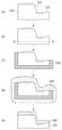
도 1은 반도체 생산 공정의 플라즈마 처리장치에서 사용되는 SiC 엣지 링의 사시도이다.1 is a perspective view of a SiC edge ring used in a plasma processing apparatus of a semiconductor production process.
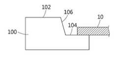
도 1에는, 반도체 생산 공정의 플라즈마 처리장치에서 사용되는 반도체 제조용 부품 중 하나인 SiC 엣지 링의, 공정 장치 제품에 따른 다양한 구조 중 일 형태(100)가 도시되어 있다. 상기 엣지 링의 단면은 상단면과 안착면의 단차있는 구조를 가지고 그 단차 간을 연결하는 단차면을 포함하는 구조를 가지는 것일 수 있다. 상기 엣지 링의 다른 일 예에서는 단차 간을 연결하는 면은 수직인 구조로 형성될 수도 있다. 상기 안착면은 피처리물의 안착면을 의미하는 것이고, 피처리물은 일 예로서 웨이퍼일 수 있다.1, one
도 2는 반도체 생산 공정의 플라즈마 처리장치에서 웨이퍼(10)가 반도체 제조용 부품 중 하나인 SiC 엣지 링(100)에 장착된 구조를 나타내는 단면도이다.2 is a cross-sectional view illustrating a structure in which a
이 때, 상기 웨이퍼는 공정 장치 구조에 따라 상기 엣지 링의 안착면(104) 전체 또는 일부에 걸치도록 장착될 수 있다. 이후 장착된 웨이퍼와 엣지 링은, 플라즈마 처리장치의 챔버 내에서 플라즈마에 노출되어 식각된다. 이 때, 외부의 플라즈마에 노출되는 부분은 식각이 진행될 수 있는데, 특히 엣지 링의 경우, 상단면(102), 단차면(106)과 안착면(104) 중 웨이퍼에 의하여 가려지지 않은 부분들에 집중적으로 식각이 진행될 수 있다. 따라서, 상기 엣지 링과 같은 플라즈마 처리장치 내의, 플라즈마에 노출되는 반도체 제조용 부품들은 손상되어 주기적인 교체를 요하게 된다. 본 발명은 이렇게 주기적으로 교체가 수행된 후 폐기의 대상이 되었던 반도체 제조용 부품 중 엣지 링에 새로운 증착부를 형성하여 적은 비용으로 새 제품을 구입하는 것과 동일한 효과를 거둘 수 있도록 함을 일 목적으로 한다.In this case, the wafer may be mounted to span the entire or part of the
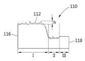
도 3은 본 발명의 일 실시예에 따르는 플라즈마 손상 부분 및 비손상 부분을 가지는 SiC 엣지 링의 제1 증착부(110)의 개략적인 구조를 도시한 단면도이다. 도 3을 보면, SiC 엣지 링의 상단면, 단차면, 안착면 중 웨이퍼에 의하여 가려지지 않은 부분들에 손상 부분(112)이 형성되었음을 확인할 수 있다. 도 3과 같이, 경우에 따라 SiC 엣지 링의 외측면(116) 및 내측면(118)은 비손상 부분을 포함할 수 있다.3 is a cross-sectional view showing a schematic structure of the
본 발명에서는, 도 3과 같이 SiC 엣지 링의 상기 제1 증착부를 편의에 따라 손상 부분이 형성된 상단면을 포함하는 제1 영역(I 구간)과, 안착면 중 손상 부분을 포함하는 제2 영역(Ⅱ 구간) 및 안착면 중 비손상 부분을 포함하는 제3 영역(Ⅲ 구간)으로 나누어 지칭하도록 한다.In the present invention, as shown in FIG. 3 , a first region (section I) including an upper surface on which a damaged portion is formed for convenience of the first deposition portion of the SiC edge ring, and a second region including a damaged portion among the seating surfaces ( Section II) and a third area (section III) including an undamaged portion of the seating surface.
본 발명의 SiC 엣지 링은, 플라즈마 손상 부분 및 비손상 부분을 가지는 SiC를 포함하는 제1 증착부; 및 상기 제1 증착부 상에 형성된 SiC를 포함하는 제2 증착부;를 포함하고, 상기 제1 증착부의 손상 부분과 상기 제2 증착부 간의 경계는 비평탄면을 포함한다.The SiC edge ring of the present invention includes: a first deposition unit comprising SiC having a plasma damaged portion and an undamaged portion; and a second deposition part including SiC formed on the first deposition part, wherein a boundary between the damaged portion of the first deposition part and the second deposition part includes a non-planar surface.
본 발명의 일 측면에 따르는 제1 증착부는, 화학적 기상 증착법에 의해 엣지 링으로 최초 제조되었던 구조체의 일부인 것일 수 있다. 본 발명의 일 측면에 따르는 제1 증착부는 플라즈마에 의해 식각된 손상 부분과 플라즈마에 의해 식각되지 않아 최초의 형태와 가공면을 유지하는 비손상 부분을 함께 포함할 수 있다.The first deposition unit according to an aspect of the present invention may be a part of a structure that was initially manufactured as an edge ring by a chemical vapor deposition method. The first deposition unit according to an aspect of the present invention may include a damaged portion etched by the plasma and an undamaged portion that is not etched by the plasma to maintain the original shape and the processed surface.
한편, 본 발명의 일 측면에 따르는 제1 증착부는 최초 제조되었던 엣지 링 상에 재생을 목적으로 하는 증착층이 적층되고 저면으로부터 가공하여 규격화되는 과정에서, 최초 제조되었던 엣지 링 구조체는 전부 가공되어 사라지고, 재생을 목적으로 적층된 증착층이 제1 증착부로 포함될 수도 있다. 즉, 본 발명의 제1 증착부는, 최초에 플라즈마에 의해 식각된 엣지 링 상에 증착된 층의 일부를 포함하는 것일 수 있다.On the other hand, the first deposition unit according to an aspect of the present invention is laminated on the edge ring that was initially manufactured and the deposition layer for the purpose of regeneration is laminated and in the process of processing and standardization from the bottom, the initially manufactured edge ring structure is all processed and disappears, , a deposition layer stacked for the purpose of regeneration may be included as the first deposition unit. That is, the first deposition unit of the present invention may include a portion of the layer deposited on the edge ring that was initially etched by plasma.
상기 제1 증착부 상에 제2 증착부가 형성될 수 있다. 본 발명의 일 측면에 따르는 제2 증착부는 제1 증착부가 플라즈마 처리장치에서 플라즈마에 의해 식각된 손상 부분과 비손상부분 상에 그대로 적층 형성될 수 있다.A second deposition part may be formed on the first deposition part. The second deposition unit according to an aspect of the present invention may be directly laminated on the damaged portion and the non-damaged portion etched by the plasma in the plasma processing apparatus by the first deposition unit.
이 때, 제1 증착부의 손상 부분과 상기 제2 증착부 간의 경계는 비평탄면을 포함할 수 있다. 본 발명에서 의미하는 비평탄면이란, 플라즈마에 의해 엣지 링이 손상되어 표면이 불규칙하게 식각된 면을 의미한다. 상기 비평탄면은, 울퉁불퉁한 요철이 형성된 표면일 수 있고, 최초 규격화된 구조체에서 일부 파편이 떨어져 나가 형성된 표면일 수도 있다. 본 발명의 비평탄면은, 최초 제조된 엣지 링 제품에 비해 플라즈마 처리 장치에서 사용되면서 플라즈마에 의해 식각되어 불균일해진 모든 측면을 다 포함하는 엣지 링 표면을 지칭하는 용어로 사용되었다.In this case, a boundary between the damaged portion of the first deposition part and the second deposition part may include a non-planar surface. The non-planar surface in the present invention means a surface on which the edge ring is damaged by plasma and the surface is irregularly etched. The non-flat surface may be a surface on which uneven irregularities are formed, or may be a surface formed by separating some fragments from the initially standardized structure. The non-planar surface of the present invention was used as a term referring to the edge ring surface including all sides that were etched by plasma and became non-uniform while being used in a plasma processing apparatus compared to the initially manufactured edge ring product.
한편, 본 발명의 일 측면에서는 상기 제1 증착부, 상기 제2 증착부 또는 이 둘은 SiC를 포함할 수 있고, 추가적으로 TaC, 하이드로카본을 포함한 다른 성분들을 더 포함할 수도 있다. 상기 하이드로카본은 CxHy의 화학식을 가지는 것으로, x가 1이상, y가 2 이상의 정수인 것을 사용할 수 있다. 또한, 상기 엣지 링은 탄화실리콘 기판에 실리콘층이 코팅된 구조일 수도 있다.Meanwhile, in one aspect of the present invention, the first deposition part, the second deposition part, or both may include SiC, and may further include other components including TaC and hydrocarbon. The hydrocarbon has a chemical formula of CxHy, and x may be an integer of 1 or more and y is an integer of 2 or more. In addition, the edge ring may have a structure in which a silicon layer is coated on a silicon carbide substrate.
또한, 상기 제1 증착부와 상기 제2 증착부는 생산될 웨이퍼와 동일한 성분을 포함할 수 있다. 상기 재생부가 제조할 웨이퍼와 전혀 상이한 성분을 포함할 경우, 플라즈마에 의해 상기 반도체 제조장치 부품이 손상될 때, 그 성분이 외부로 유출되어 웨이퍼를 오염시킬 수 있기 때문이다. SiC 엣지 링의 제1 증착부와 제2 증착부의 구성 원소 및 성분 분포는 같을 수도 있고, 다를 수도 있다. 즉, 상기 비재생부, 상기 재생부 또는 이 둘은 SiC 뿐 아니라 TaC, 하이드로카본 등 추가적 성분들을 포함함으로써, 굴곡강도가 월등히 높아질 수 있고, 플라즈마에 대한 더 높은 내식성을 확보할 수 있다.In addition, the first deposition unit and the second deposition unit may include the same component as the wafer to be produced. This is because, when the regenerator includes a component completely different from the wafer to be manufactured, the component may leak to the outside and contaminate the wafer when the component of the semiconductor manufacturing apparatus is damaged by plasma. The constituent elements and component distributions of the first deposition part and the second deposition part of the SiC edge ring may be the same or different. That is, since the non-regenerated part, the regenerated part, or the two contain additional components such as TaC and hydrocarbon as well as SiC, the flexural strength can be significantly increased, and higher corrosion resistance to plasma can be secured.
본 발명의 일 실시예에 따르면, 상기 비평탄면은 플라즈마 식각에 의하여 형성된 것일 수 있다.According to an embodiment of the present invention, the non-planar surface may be formed by plasma etching.
본 발명의 일 실시예에 따르면, 상기 비평탄면 중, 플라즈마에 노출되어 손상되기 전 동일한 높이이던 부분으로부터 형성된 비평탄면의 최고점과 최저점의 높이차(도 3의 h)는, 0.01 mm 내지 3 mm(실질적으로 3 mm 이하) 인 것일 수 있다. 일 예로서, 상기 높이차는 0.5 mm 내지 3 mm 인 것일 수 있다.According to an embodiment of the present invention, the height difference between the highest point and the lowest point of the non-flat surface formed from the portion that was at the same height before being exposed to plasma and damaged ( substantially 3 mm or less). As an example, the height difference may be 0.5 mm to 3 mm.
본 발명의 일 실시예에 따르면, 상기 비평탄면의 표면 조도는, 0.1 ㎛ 내지 2.5 ㎛ 인 것일 수 있다.According to an embodiment of the present invention, the surface roughness of the non-planar surface may be 0.1 μm to 2.5 μm.
일 예로서, 상기 비평탄면은, 플라즈마에 의해 표면이 식각된 직후의 표면 조도가 0.05 ㎛ 내지 0.3 ㎛ 인 것일 수 있다. 또한, 다른 일 예로서, 상기 비평탄면은, 플라즈마에 의해 표면이 식각된 후, 손상된 표면의 일부를 가공함으로써 표면 조도가 0.1 ㎛ 내지 2.5 ㎛ 인 수준으로 형성한 것일 수 있다.As an example, the non-planar surface may have a surface roughness of 0.05 μm to 0.3 μm immediately after the surface is etched by plasma. In addition, as another example, the non-planar surface may have a surface roughness of 0.1 μm to 2.5 μm by processing a part of the damaged surface after the surface is etched by plasma.
일 예에 따르면, 별도의 가공 단계를 포함하지 않더라도 상기 제1 증착부의 표면 조도 값이 0.1 ㎛ 내지 2.5 ㎛ 수준으로 형성될 때, 제2 증착부는 제1 증착부의 표층 상에 균질한 증착층을 형성할 수 있다.According to an example, even if a separate processing step is not included, when the surface roughness value of the first deposition part is formed at a level of 0.1 μm to 2.5 μm, the second deposition part forms a homogeneous deposition layer on the surface layer of the first deposition part. can do.
본 발명의 일 실시예에 따르면, 상기 제1 증착부와 상기 제2 증착부의 광 투과도는 상이한 것일 수 있다.According to an embodiment of the present invention, the light transmittance of the first deposition part and the second deposition part may be different.
본 발명에서 의미하는 광 투과도는 물질층을 빛이 통과하는 정도로서, 물질층을 통과하여 나온 빛의 세기를 물질층에 대한 입사광의 세기로 나눈 값에 해당한다. 광 투과도는 다양한 방법으로 측정될 수 있으나, 3 mm 두께로 시편을 제작하고 광도 150 Lux 이상의 광원을 이용하여 시편과 광원과의 거리가 7 cm 이내에서 측정한 것일 수 있다. 두께나 광원, 시편과 광원과의 거리에 따라 광 투과도는 달라지게 되므로, 광 투과도는 동일한 두께인 경우의 상대값으로 고려될 수 있다. 따라서, 광 투과도는 물질의 고유한 특징에 해당하며, 동일한 성분 및 조성을 가진 소재라도 그 결정 구조나 상에 따라 서로 다른 광 투과도를 가질 수 있다.In the present invention, light transmittance is the degree to which light passes through the material layer, and corresponds to a value obtained by dividing the intensity of light emitted through the material layer by the intensity of incident light on the material layer. The light transmittance can be measured in various ways, but it may be measured within 7 cm between the specimen and the light source using a light source with a luminosity of 150 Lux or higher after making a specimen with a thickness of 3 mm. Since the light transmittance varies depending on the thickness, the light source, and the distance between the specimen and the light source, the light transmittance may be considered as a relative value in the case of the same thickness. Therefore, light transmittance corresponds to a unique characteristic of a material, and even materials having the same component and composition may have different light transmittances depending on the crystal structure or phase thereof.
본 발명의 일 측면에서 제공하는 SiC 엣지 링의 제1 증착부와 제2 증착부는 포함하는 성분이 서로 동일하더라도, 각각의 광 투과도가 상이한 것일 수 있다.Although the components included in the first deposition part and the second deposition part of the SiC edge ring provided in an aspect of the present invention are the same, the respective light transmittances may be different.
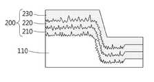
도 4는 본 발명의 일 실시예에 따르는 SiC 엣지 링의 제1 증착부(110) 상에 제2 증착부(210)가 형성되고 제2 증착부 상에 제3 증착부가 복수 층(220, 230)으로 형성된 개략적인 구조를 도시한 단면도이다.4 shows a
도 4와 같이, 제3 증착부는 복수의 층으로 형성될 수 있다. 즉, 본 발명의 일 측면에 따르면, 제2 증착부 상에 제1의 제3 증착부(220)가 형성되고, 제1의 제3 증착부 상에 제2의 제3 증착부(230)가 형성될 수 있다. 이 때 제1의 제3 증착부가 형성되고 엣지 링으로 규격화된 후에, 규격화된 엣지 링이 플라즈마 처리장치에서 사용될 수 있다. 이 때, 제1의 제3 증착부의 일부 표면은 식각 되고, 손상 부분이 형성된 제1의 제3 증착부 상에 제2의 제3 증착부가 형성되어 본 발명의 일 측면에서 제공하는 복수 층의 제3 증착부를 포함하는 SiC 엣지 링이 확보될 수 있다.4 , the third deposition unit may be formed of a plurality of layers. That is, according to an aspect of the present invention, the first
본 발명의 일 실시예에 따르면, 상기 제1 증착부는, 그라파이트, 반응소결 SiC, 상압소결 SiC, 핫프레스 SiC, 재결정 SiC, CVD SiC, TaC 및 YaC로 이루어진 군에서 선택되는 적어도 어느 하나를 포함하는 것일 수 있다.According to an embodiment of the present invention, the first deposition unit includes at least one selected from the group consisting of graphite, reaction sintered SiC, atmospheric pressure sintered SiC, hot press SiC, recrystallized SiC, CVD SiC, TaC and YaC. it could be
본 발명의 일 측에 따르면, 상기 제1 증착부(비재생부)의 소재는, 반도체 제조용 장비 등에 이용될 수 있는 부품에 적용가능한 소재라면 그 종류를 특별히 한정하지 아니한다. 일 예로서, 모재로서 이용 가능한 소재인 그라파이트를 포함하는 탄소 소재, 내플라즈마 특성이 우수한 다양한 SiC 소재, 다양한 TaC 또는 YaC 소재 중 하나 이상을 포함하도록 형성되는 것일 수 있다.According to an aspect of the present invention, the material of the first deposition part (non-regeneration part) is not particularly limited as long as it is a material applicable to parts that can be used in equipment for semiconductor manufacturing and the like. As an example, it may be formed to include one or more of a carbon material including graphite, which is a material available as a base material, various SiC materials having excellent plasma resistance, and various TaC or YaC materials.
본 발명의 일 측에 따르면, 상기 제2 증착부(재생부)는, 내플라즈마 특성이 우수하도록 SiC, TaC 또는 둘 다를 포함하는 것일 수 있다.According to an aspect of the present invention, the second deposition unit (regeneration unit) may include SiC, TaC, or both to have excellent plasma resistance.
본 발명의 일 실시예에 따르면, 제1 증착부 및 제2 증착부의 광 투과도의 차이는, 상기 제2 증착부 내의 복수 개의 적층된 층 간의 광 투과도의 차이보다 큰 것일 수 있다.According to an embodiment of the present invention, a difference in light transmittance between the first deposition unit and the second deposition unit may be greater than a difference in light transmittance between a plurality of stacked layers in the second deposition unit.
본 발명의 일 실시예에 따르면, 상기 제1 증착부는 복수 개의 적층된 층을 포함하고, 상기 제1 증착부의 복수 개의 적층된 층의 층 간의 경계에서는 광 투과도가 점진적으로 변화하는 것일 수 있다.According to an embodiment of the present invention, the first deposition part may include a plurality of stacked layers, and the light transmittance may be gradually changed at a boundary between the layers of the plurality of stacked layers of the first deposition part.
본 발명의 일 예에 따라서, 제1 증착부를 복수 개의 층으로 형성할 경우, 적층된 제1 증착부의 층 간의 경계에서는 광 투과도가 점진적으로 변화하는 특징이 구현될 수 있다.According to an example of the present invention, when the first deposition unit is formed of a plurality of layers, a characteristic in which light transmittance is gradually changed at the boundary between the layers of the stacked first deposition unit may be implemented.
본 발명의 일 실시예에 따르면, 상기 제2 증착부 상에 형성된 제3 증착부를 더 포함하고, 상기 제2 증착부와 상기 제3 증착부 간의 경계면은 비평탄면을 포함하는 것일 수 있다.According to an embodiment of the present invention, a third deposition part formed on the second deposition part may be further included, and an interface between the second deposition part and the third deposition part may include a non-planar surface.
본 발명의 일 측면에서는 제2 증착부 상에 제3 증착부가 더 형성될 수도 있다. 이 때 제2 증착부와 제3 증착부 간의 경계면은 비평탄면을 포함할 수 있는데, 이는 앞서 설명한 것과 같이 제2 증착부가 형성된 후, 제2 증착부의 일부 표면이 플라즈마에 의해 식각 되었기 때문이다. 즉, 본 발명의 일 측면에 따르는 SiC 엣지 링은, 제1 증착부 상에 제2 증착부가 형성된 후에 규격화되어 엣지 링으로 제조되고 플라즈마 처리장치에서 사용되면서 제2 증착부 표면의 적어도 일부가 식각된 후, 식각된 일부 손상 부분을 포함하는 제2 증착부 상에 제3 증착부가 형성된 것일 수 있다.In an aspect of the present invention, a third deposition part may be further formed on the second deposition part. In this case, the interface between the second deposition part and the third deposition part may include a non-planar surface, because as described above, after the second deposition part is formed, some surfaces of the second deposition part are etched by plasma. That is, the SiC edge ring according to an aspect of the present invention is standardized after the second deposition part is formed on the first deposition part, is manufactured as an edge ring, and at least a part of the surface of the second deposition part is etched while being used in a plasma processing apparatus. Afterwards, the third deposition part may be formed on the second deposition part including the etched damaged part.
본 발명의 일 실시예에 따르면, 상기 제1 증착부, 상기 제2 증착부 및 제3 증착부의 광 투과도는 각각 상이한 것일 수 있다.According to an embodiment of the present invention, the light transmittance of the first deposition part, the second deposition part, and the third deposition part may be different from each other.
제1 증착부와 제2 증착부 간의 광 투과도가 상이할 수 있는 것처럼, 제1 증착부, 제2 증착부 및 제3 증착부의 광 투과도 또한 각각 상이한 것일 수 있다. 제3 증착부 또한, 제1 증착부 및 제2 증착부와 구성 성분이 같을 수 있으나, 광 투과도가 각각과 상이한 것일 수 있다.Just as light transmittance between the first deposition unit and the second deposition unit may be different, the light transmittance of the first deposition unit, the second deposition unit, and the third deposition unit may also be different. The third deposition part may also have the same components as the first deposition part and the second deposition part, but light transmittance may be different from each other.
또한, 본 발명의 일 실시예에 따르면, 상기 제2 증착부 상에 형성된 제3 증착부를 더 포함하고, 상기 재생된 SiC 엣지 링의 단면에 있어서, 상기 제1 증착부와 상기 제2 증착부 간의 경계선과, 상기 제2 증착부와 상기 제3 증착부 간의 경계선은 서로 평행을 이루는 구간을 포함하는 것일 수 있다.In addition, according to an embodiment of the present invention, further comprising a third deposition part formed on the second deposition part, in the cross section of the regenerated SiC edge ring, between the first deposition part and the second deposition part The boundary line and the boundary line between the second deposition unit and the third deposition unit may include sections that are parallel to each other.
상기 서로 평행을 이루는 구간은, 각 증착부가 플라즈마에 의해 손상되지 않은 영역에 형성될 수 있다. 제1 증착부 중 플라즈마에 의해 손상되지 않은 부분 위로는, 그 경계와 평행한 상면을 형성하도록 제2 증착부가 형성될 수 있다. 또한, 제2 증착부가 형성된 후, 플라즈마에 노출된다 하더라도, 플라즈마에 의해 손상되지 않은 부분 위로는, 그 경계와 평행한 상면을 형성하도록 제3 증착부가 형성될 수 있는 것이다.The sections that are parallel to each other may be formed in a region where each deposition unit is not damaged by the plasma. A second deposition part may be formed over a portion of the first deposition part that is not damaged by the plasma so as to form an upper surface parallel to the boundary thereof. In addition, after the second deposition part is formed, even if exposed to plasma, the third deposition part may be formed over a portion not damaged by the plasma to form an upper surface parallel to the boundary.
도 4에 도시된 바와 같이, 플라즈마로부터 웨이퍼 표면에 의해 가리워지는 등의 이유로 비손상부를 포함하는 SiC 엣지 링의 일부 표면은 평탄한 면을 형성하게 된다. 이 부분에 적층된 제1 증착부, 제2 증착부, 제3 증착부 간의 SiC 엣지 링 단면의 경계선은 서로 평행을 형성할 수 있다. 따라서 본 발명의 일 측면에서 제공하는 SiC 엣지 링은 상기 제1 증착부와 상기 제2 증착부 간의 경계선과, 상기 제2 증착부와 상기 제3 증착부 간의 경계선이 서로 평행을 이루는 구간을 포함하는 것일 수 있다. 상기 제3 증착부가 복수 층으로 형성되는 경우에는, 상기 제3 증착부의 복수 층 간의 경계면은 서로 평행을 이루는 구간을 포함하는 것일 수 있다.As shown in FIG. 4 , some surfaces of the SiC edge ring including the undamaged portion form a flat surface for reasons such as being obscured by the wafer surface from the plasma. The boundary lines of the SiC edge ring cross-sections between the first deposition part, the second deposition part, and the third deposition part stacked on this part may be parallel to each other. Therefore, the SiC edge ring provided in one aspect of the present invention includes a section in which a boundary line between the first deposition part and the second deposition part and a boundary line between the second deposition part and the third deposition part are parallel to each other. it could be When the third deposition part is formed of a plurality of layers, the boundary surfaces between the plurality of layers of the third deposition part may include sections that are parallel to each other.
본 발명의 일 측면에 따르면 상기 제1 증착부와 제2 증착부 간의 경계면과, 상기 제2 증착부와 제3 증착부 간의 경계면, 제3 증착부가 복수 층으로 형성되었을 경우 각 층간의 경계면은 각각이 평행하도록 형성된 부분을 포함할 수도 있다.According to an aspect of the present invention, the interface between the first deposition part and the second deposition part, the interface between the second deposition part and the third deposition part, and the interface between the layers when the third deposition part is formed in a plurality of layers are respectively It may include portions formed so as to be parallel to each other.
본 발명의 일 측면에 따르면, 상기 SiC 엣지 링에 증착부를 형성한 후, 플라즈마 처리장치에서 사용하기 위해 규격화하는 작업이 수행될 수 있다. 본 발명에서 수행되는 상기 규격화하는 작업은 일 예로서, 증착부가 형성된 SiC 엣지 링을 저면을 가공하는 것일 수 있다. 즉, 본 발명의 일 측면에 따르면, 증착부가 엣지 링 상부로 적층되어 두께가 두꺼워진 만큼 아래로부터 저면을 가공함으로써 플라즈마 처리장치에 적용할 수 있는 제품의 크기에 맞게 규격화가 되는 것이다.According to an aspect of the present invention, after forming a deposition part on the SiC edge ring, a standardization operation for use in a plasma processing apparatus may be performed. The standardizing operation performed in the present invention may be, for example, processing the bottom surface of the SiC edge ring on which the deposition part is formed. That is, according to one aspect of the present invention, by processing the bottom surface from the bottom as much as the deposition portion is laminated on the edge ring and thickened, it is standardized according to the size of the product applicable to the plasma processing apparatus.
이 과정에서, 플라즈마에 식각된 엣지 링은, 일 예로서 도 3에 도시된 것 같은 엣지 링(110)의 구조를 형성하게 될 수 있다. 본 발명의 일 측면에 따르면 이러한 엣지 링 상에 도 4와 같이 복수의 증착부가 층을 형성하여 얹어질 수 있을 것이다. 그 다음, 저면으로부터 일정 두께만큼 가공되어 규격화 될 경우, 규격화된 엣지 링에는 도 5와 같은 단면 구조가 형성될 수 있다.In this process, the edge ring etched in the plasma may form a structure of the
도 5a 및 도 5b는 본 발명의 다른 일 실시예에 따르는, SiC 엣지 링의 제1 증착부 상에 제2 증착부가 형성되고, 제2 증착부 상에 제3 증착부가 복수 층으로 형성된 개략적인 구조를 도시한 단면도이다.5A and 5B are schematic structures in which a second deposition part is formed on a first deposition part of a SiC edge ring, and a third deposition part is formed in a plurality of layers on the second deposition part, according to another embodiment of the present invention; is a cross-sectional view showing
본 발명의 일 실시예에 따르면, 상기 제1 증착부는 분리된 적어도 두 개의 구조체를 포함하는 것일 수 있다.According to an embodiment of the present invention, the first deposition unit may include at least two separated structures.
도 5a에는 SiC 엣지 링이 저면으로부터 일정 두께만큼 가공됨으로 인해 제1 증착부(110)가 분리된 두 개의 구조체(110')로 나뉘어 있는 SiC 엣지 링의 단면도가 도시되어 있다.5A is a cross-sectional view of the SiC edge ring in which the
한편, 도 5a에는 제3 증착부가 두 층(220, 230)으로 형성되어 있는데, 이 때 제3 증착부의 각 층은 증착 두께가 동일할 필요는 없다. 본 발명의 일 측면에서는 저면으로부터 가공되는 정도를 고려하여 필요에 따라 다른 제3 증착부 층(220)보다 특별히 더 두꺼운 제3 증착부 층(230)을 형성할 수도 있다.Meanwhile, in FIG. 5A , the third deposition unit is formed of two
본 발명의 일 실시예에 따르면, 상기 제2 증착부(210)는 분리된 적어도 두 개의 구조체(210')를 포함하는 것일 수 있다.According to an embodiment of the present invention, the
도 5b에는 SiC 엣지 링이 저면으로부터 일정 두께만큼 가공됨으로 인해 제1 증착부(110) 뿐 아니라 제2 증착부(210) 까지도 분리되어 두 개의 구조체로 나뉘어 있는 SiC 엣지 링의 단면도가 도시되어 있다.5B is a cross-sectional view of the SiC edge ring divided into two structures by separating the
한편, 도 5b에는 제3 증착부가 세 층(220, 230, 240)으로 형성되어 있는데, 이 때 각 층의 증착 두께는 저면으로부터 가공되는 정도를 고려하여 필요에 따라 형성할 수 있다.Meanwhile, in FIG. 5B , the third deposition unit is formed of three
본 발명의 일 실시예에 따르면, 상기 분리된 적어도 두 개의 구조체는 동일한 광 투과도를 가지는 것일 수 있다.According to an embodiment of the present invention, the at least two separated structures may have the same light transmittance.
동일한 챔버의 동일한 증착 조건에서 증착된 구조체는 동일한 광 투과도를 형성할 수 있다. 즉, 동일한 원료가스로부터 동시간에 형성된 증착 구조체는 빛의 광 투과도가 같은 특징을 보유할 수 있다.Structures deposited under the same deposition conditions in the same chamber may have the same light transmittance. That is, the deposition structures formed at the same time from the same source gas may have the same light transmittance characteristics.
도 5a의 분리된 제1 증착층, 도 5b의 분리된 제1 증착층 및 제2 증착층은 각각이 서로 연결된 하나의 구조체로 증착된 후, 저면으로부터 일정 두께가 가공되면서 서로 분리된 구조체에 해당한다. 따라서, 상기 도 5a의 분리된 제1 증착층, 도 5b의 분리된 제1 증착층 및 제2 증착층은 각각이 동일한 광 투과도를 형성할 수 있게 된다.The separated first deposition layer of FIG. 5A, the separated first deposition layer and the second deposition layer of FIG. 5B correspond to structures separated from each other while being processed to a certain thickness from the bottom after being deposited as one structure connected to each other do. Accordingly, the separated first deposition layer of FIG. 5A , the separated first deposition layer and the second deposition layer of FIG. 5B may each have the same light transmittance.
본 발명의 일 실시예에 따르면, 상기 제1 증착부는 분리되지 않은 하나의 구조체를 형성하고, 상기 제1 증착부의 단면은, 상기 SiC 엣지 링의 외측면으로부터 내측면에 이르기까지 제1 영역 내지 제3 영역을 포함하고, 상기 제1 영역의 평균 두께 t1, 상기 제2 영역의 평균 두께 t2 및 상기 제3 영역의 평균 두께 t3는, t1 > t3 > t2 인 것일 수 있다.According to an embodiment of the present invention, the first deposition part forms a single structure that is not separated, and the cross-section of the first deposition part is from the first region to the first region from the outer surface to the inner surface of the SiC edge ring. It includes three regions, and the average thickness t1 of the first region, the average thickness t2 of the second region, and the average thickness t3 of the third region may be t1 > t3 > t2.
도 3에는, 본 발명의 일 예에 따르는 SiC 엣지 링의 제1 영역 내지 제3 영역이 구분되어 있다. SiC 엣지 링의 상기 제1 증착부의 단면을 편의에 따라 손상 부분이 형성된 상단면을 포함하는 제1 영역(I 구간)과, 안착면 중 손상 부분을 포함하는 제2 영역(Ⅱ 구간) 및 안착면 중 비손상 부분을 포함하는 제3 영역(Ⅲ 구간)으로 나누어 지칭하도록 한다. 경우에 따라 상기 제1 영역에는 상단면과 안착면을 연결하는 단차면이 포함될 수 있다. 이 때, 본 발명의 일 측면에 따르면, 각 영역의 평균 두께를 t1 내지 t3라고 할 때, t1 내지 t3의 관계는 t1 > t3 > t2 인 것일 수 있다.In Figure 3, the first region to the third region of the SiC edge ring according to an embodiment of the present invention is divided. For convenience, the cross-section of the first deposition part of the SiC edge ring includes a first region (section I) including an upper surface on which a damaged portion is formed, a second region (section II) including a damaged portion among the seating surfaces, and a seating surface It will be divided into a third region (section III) including the non-damaged portion. In some cases, the first region may include a stepped surface connecting the top surface and the seating surface. At this time, according to an aspect of the present invention, when the average thickness of each region is t1 to t3, the relationship between t1 to t3 may be t1 > t3 > t2.
본 발명의 일 실시예에 따르면, 상기 제2 증착부의 평균 두께는 0.5 mm 내지 3 mm 두께 인 것일 수 있다.According to an embodiment of the present invention, the average thickness of the second deposition portion may be 0.5 mm to 3 mm thick.
일 예에서는, 상기 제2 증착부의 평균 두께는 0.7 mm 내지 2.5 mm 인 것일 수 있다.In one example, the average thickness of the second deposition portion may be 0.7 mm to 2.5 mm.
본 발명의 일 측면에 따르면 상기 제2 증착부를 형성하는 과정에서, 제2 증착부를 적절한 두께로 형성하는 것이 중요할 수 있다. 상기 재생부가 지나치게 얇게 형성될 경우, 플라즈마에 의해 재생부가 모두 식각되어 아래 층의 비재생부의 손상 부분이 노출될 수 있다. 이는 플라즈마 처리 기법 과정에서 생산되는 반도체 제품의 품질을 저하시키는 직접적인 원인이 될 수 있다. 또한 상기 재생부가 지나치게 두껍게 형성될 경우 증착되어 재생부를 형성하는 원료의 낭비가 심해지고, 가공에 소비되는 비용과 노력이 증가하게 되어 최종적으로 반도체 제품의 단가를 상승시키고 생산 효율을 저하시키는 문제를 발생시킬 수 있다. 따라서, 본 발명의 일 측면에서는 재생부의 두께를 적절하게 제어하는 것이 중요한 요소가 될 수 있다.According to an aspect of the present invention, in the process of forming the second deposition part, it may be important to form the second deposition part to an appropriate thickness. When the regenerated portion is formed to be too thin, the regenerated portion is all etched by the plasma, and a damaged portion of the non-regenerated portion of a lower layer may be exposed. This may be a direct cause of lowering the quality of semiconductor products produced during plasma processing. In addition, if the regenerated portion is formed too thickly, the waste of raw materials that are deposited and form the reclaimed portion increases, and the cost and effort consumed in processing increases, ultimately raising the unit price of the semiconductor product and lowering the production efficiency. can do it Accordingly, in one aspect of the present invention, it may be an important factor to appropriately control the thickness of the reproduction unit.
통상적인 플라즈마 처리장치에서 교체를 요하는 엣지 링의 경우 0.5 mm 내외로 식각이 발생하는 이러한 측면까지 고려해볼 때 본 발명의 일 측면에서 다양한 실험을 통해 확인한, 상기 제2 증착부의 평균 두께는 0.5 mm 내지 3 mm 두께 인 것이 좋다.In the case of an edge ring requiring replacement in a conventional plasma processing apparatus, the average thickness of the second deposition portion, confirmed through various experiments in one aspect of the present invention, is 0.5 mm considering this aspect in which etching occurs to around 0.5 mm. to 3 mm thick.
본 발명의 일 실시예에 따르면, 상기 비평탄면은 상기 제2 증착부가 형성되기 전 표면 가공 처리가 수행된 것일 수 있다.According to an embodiment of the present invention, the non-planar surface may have been subjected to surface processing before the second deposition part is formed.
아래에서는 본 발명의 일 실시예에서 제공하는 SiC 엣지 링의 제조방법을 설명한다.Hereinafter, a method of manufacturing a SiC edge ring provided in an embodiment of the present invention will be described.
본 발명의 SiC 엣지 링은, 플라즈마 손상 부분 및 비손상 부분을 포함하는 엣지 링을 준비하는 단계; 상기 준비된 SiC 엣지 링의 일부를 마스킹하는 단계; 상기 일부가 마스킹된 SiC 엣지 링에 화학적 기상 증착법으로 재생부를 형성하는 단계; 및 상기 마스킹을 제거하고, 상기 재생부가 형성된 SiC 엣지 링을 규격화 가공하는 단계;를 포함한다. 여기서 설명하는 재생부는, 본 발명의 제2 증착부 또는 제3 증착부가 될 수 있고, 경우에 따라 제1 증착부 또한 여기서 설명하는 재생부에 포함될 수 있다.The SiC edge ring of the present invention comprises the steps of: preparing an edge ring including a plasma damaged portion and an undamaged portion; masking a part of the prepared SiC edge ring; forming a regenerated portion on the partially masked SiC edge ring by chemical vapor deposition; and removing the masking and standardizing the SiC edge ring on which the regenerated part is formed. The regeneration unit described herein may be the second deposition unit or the third deposition unit of the present invention, and in some cases, the first deposition unit may also be included in the regeneration unit described herein.
아래에서 설명하는 SiC 엣지 링의 제조방법은, 반도체 제품을 제조하기 위한 플라즈마 처리장치에서 플라즈마에 노출되어 식각된 후 주기적인 교체를 요하는 부품에 모두 적용할 수 있다.The manufacturing method of the SiC edge ring to be described below can be applied to any part requiring periodic replacement after being exposed to plasma and etched in a plasma processing apparatus for manufacturing a semiconductor product.
도 6은 본 발명의 일 실시예에 따라, SiC 엣지 링의 제1 증착부 상에 제2 증착부가 형성되는 과정을 개략적으로 나타낸 단면 공정도이다.6 is a cross-sectional process diagram schematically illustrating a process in which a second deposition part is formed on a first deposition part of a SiC edge ring according to an embodiment of the present invention.
도 6과 같이 본 발명의 일 실시예에 따르면, 마스킹하는 단계를 포함하지 않고, SiC 엣지 링의 제1 증착부 상에 곧바로 제2 증착부를 형성할 수 있다.According to an embodiment of the present invention as shown in FIG. 6 , the second deposition part may be directly formed on the first deposition part of the SiC edge ring without a masking step.
도 7은 본 발명의 일 실시예에 따라, 마스킹하는 단계를 포함하여 SiC 엣지 링의 제1 증착부 상에 제2 증착부가 형성되는 과정을 개략적으로 나타낸 단면 공정도이다.7 is a cross-sectional process diagram schematically illustrating a process of forming a second deposition part on the first deposition part of the SiC edge ring, including the step of masking, according to an embodiment of the present invention.
도 6 및 도 7에서는 본 발명의 일 실시예에 따라 제3 증착부를 형성하기 전에 제2 증착부가 형성되는 과정까지를 도시하고 있다.6 and 7 illustrate a process in which the second deposition part is formed before the third deposition part is formed according to an embodiment of the present invention.
아래에서는 도 7에 도시된 SiC 엣지 링의 단면 구조를 통해 본 발명의 일 실시예에서 제공하는 제1 증착부 상에 제2 증착부가 형성되는 각 단계를 설명한다.Below, each step of forming the second deposition part on the first deposition part provided in an embodiment of the present invention through the cross-sectional structure of the SiC edge ring shown in FIG. 7 will be described.
도 7(a)에는 플라즈마 손상 부분 및 비손상 부분을 포함하는 SiC 엣지 링을 준비하는 단계가 도시되어 있다.7( a ) shows a step of preparing a SiC edge ring including a plasma damaged portion and an undamaged portion.
도 7(a)은 SiC 엣지 링의 일 예로서, 건식식각장치 내에서 플라즈마에 의해 식각되어 손상 부분(112)과, 플라즈마에 노출되지 않아 식각되지 않은 비손상 부분(114)을 포함하는 손상된 엣지 링(110)의 단면이 도시되어 있다. 도 7(a)에서 플라즈마에 의해 식각되어 손상 부분(112)은 도 2의 손상 전의 엣지 링과 비교해볼 때, 상단면, 단차면 및 웨이퍼에 의해 가리워지지 않은 안착면의 일부에 형성될 수 있다. 안착면의 나머지 일부(114)는 웨이퍼에 의해 가리워져서 플라즈마로부터 보호되어 비손상 부분을 형성할 수 있다.도 7(b)에는 상기 준비된 SiC 엣지 링의 일부를 마스킹(410)하는 단계가 도시되어 있다.7 (a) is an example of a SiC edge ring, a damaged edge including a damaged
상기 마스킹하는 단계는, 화학적 기상 증착법에 의한 증착 과정에서, 비손상 부분을 포함하는 영역에 마스킹을 형성하는 것일 수 있다. 이는 재생부(제2 증착부)를 형성하는 단계에서 증착이 불요한 부분에의 원료 가스의 증착을 최소화하여 증착 후의 가공을 최소화하기 위한 것이다. 즉, 이러한 마스킹하는 단계는 본 발명의 SiC 엣지 링을 제조하는 공정의 효율을 향상시키기 위해 수행되는 것이다.The masking may include forming a mask in a region including an undamaged portion during a deposition process using a chemical vapor deposition method. This is to minimize the deposition of the source gas on the portion where deposition is unnecessary in the step of forming the regeneration unit (the second deposition unit), thereby minimizing post-deposition processing. That is, this masking step is performed to improve the efficiency of the process for manufacturing the SiC edge ring of the present invention.
이 때, 상기 재생부의 성분으로는 가공이 어려운 SiC, TaC 등과 같은 물질이 포함될 수 있기 때문에, 이 후의 규격화 가공을 수행하는 과정에서 직접적인 재생부의 가공 면적을 최소화하는 것이 제품의 생산성을 확보하는데 대단히 중요할 수 있다. 본 발명의 일 측면에서는, 이 후의 규격화 가공하는 단계에서의 편의성 확보를 위해 비손상면을 포함하는 부분에 마스킹하는 구성을 포함할 수 있다.At this time, since materials such as SiC and TaC, which are difficult to process, may be included as components of the regenerated part, it is very important to ensure the productivity of the product to minimize the processing area of the direct regenerated part in the process of performing the subsequent standardization processing. can do. In one aspect of the present invention, it may include a configuration for masking the portion including the undamaged surface in order to secure convenience in the subsequent standardization processing step.
본 발명의 일 예에 따르면, 상기 마스킹하는 단계는, SiC 엣지 링의 저면, 외측면 및 내측면으로 이루어진 군에서 선택되는 하나 이상의 비손상 면을 마스킹하는 것을 포함하는 것일 수 있다. 본 발명의 반도체 제조용 부품의 일 예인 엣지 링을 예로 들어 설명하면, 도 7(b)와 같이 비손상면 부분에 해당하는 저면, 외측면 및 내측면 중 하나 이상에 마스킹이 형성될 수 있다.According to an example of the present invention, the masking may include masking one or more intact surfaces selected from the group consisting of a bottom surface, an outer surface, and an inner surface of the SiC edge ring. Taking the edge ring as an example of the semiconductor manufacturing component of the present invention as an example, a masking may be formed on one or more of the bottom surface, the outer surface, and the inner surface corresponding to the non-damaged surface portion as shown in FIG. 7( b ).
상기 마스킹의 소재로는, 그라파이트 소재의 재료를 비롯한, 재생부에 포함되는 증착 물질보다 가공이 용이한 재료를 사용할 수 있다. 이로써, 이 후의 가공하는 단계에서, 증착 물질이 곧바로 형성된 부분 보다, 마스킹한 부분이 더 쉽게 가공될 수 있는 효과가 있다. 즉, 마스킹하는 단계를 본 발명의 SiC 엣지 링의 제조방법에 포함함으로써, 재생된 SiC 엣지 링의 규격화된 면을 손쉽게 확보할 수 있는 장점이 있다.As the material for the masking, a material that is easier to process than a deposition material included in the regeneration unit, including a graphite material, may be used. Accordingly, in the subsequent processing step, there is an effect that the masked portion can be more easily processed than the portion where the deposition material is directly formed. That is, by including the masking step in the manufacturing method of the SiC edge ring of the present invention, there is an advantage in that the standardized surface of the regenerated SiC edge ring can be easily secured.
도 7(c)에는 상기 일부가 마스킹된 SiC 엣지 링에 화학적 기상 증착법으로 재생부(300)(제2 증착부)를 형성하는 단계가 도시되어 있다.7( c ) shows a step of forming the regeneration unit 300 (the second deposition unit) on the partially masked SiC edge ring by chemical vapor deposition.
본 단계에서는 화학적 기상 증착법에 따라, 챔버 내에 일부가 마스킹된 SiC 엣지 링이 장착된 상태에서, 원료 가스가 장착된 SiC 엣지 링에 증착되어 제1 증착부 상에 재생부(제2 증착부)가 형성되는 것이다.In this step, according to the chemical vapor deposition method, in a state where the partially masked SiC edge ring is mounted in the chamber, the source gas is deposited on the mounted SiC edge ring, and the regeneration unit (the second deposition unit) is formed on the first deposition unit. will be formed
도 7(c)와 같이, 플라즈마에 의해 식각된 SiC 엣지 링의 손상 부분은 평탄하고 고르지 않은 면을 포함할 수 있다. 이 때, 본 발명은 플라즈마에 의해 식각된 SiC 엣지 링의 손상 부분을 별도로 평탄하게 선 가공하지 않고 재생부를 형성하는 것을 특징으로 한다. 이로 인해 본 발명의 일 측면에 따르면 추가될 수 있는 별도의 표면 가공 단계가 생략되어 전체 공정의 속도가 상승하고 재생 공정에서 비용을 절감하는 효과가 생길 수 있다.As shown in FIG. 7C , the damaged portion of the SiC edge ring etched by the plasma may include a flat and uneven surface. At this time, the present invention is characterized in that the regenerated portion is formed without separately flattening the damaged portion of the SiC edge ring etched by plasma. For this reason, according to an aspect of the present invention, a separate surface processing step that may be added is omitted, thereby increasing the speed of the entire process and reducing costs in the regeneration process.
상기 재생부를 형성하는 단계의 구체적인 방법으로는, 증착 온도 1000 ℃ 내지 1500 ℃ 에서, 성막 속도를 20 ㎛/hour 내지 400 ㎛/hour로 원료 가스의 체류시간을 7 초 내지 110 초로 할 수 있다. 도 7(c)와 같이, 상기 재생부가 형성된 SiC 엣지 링은, 현장에서 요구되는 제품의 규격에 맞지 않게 가공되지 않은 형태일 수 있다.As a specific method of forming the regeneration unit, at a deposition temperature of 1000° C. to 1500° C., a deposition rate of 20 μm/hour to 400 μm/hour, and a residence time of the source gas can be 7 seconds to 110 seconds. As shown in FIG. 7( c ), the SiC edge ring on which the regenerated part is formed may be in a form that is not processed to meet the specifications of products required in the field.
재생부가 형성된 SiC 엣지 링은 이후 마스킹을 제거하는 공정과 규격화 가공하는 공정이 수행될 수 있다. 이 때, 마스킹을 제거하는 공정과 규격화 가공하는 공정은 동시에 수행될 수도 있고, 두 공정 중 어느 하나의 공정이 먼저 수행된 후 나머지 공정이 수행될 수도 있다. 이 때, 비재생부 일부에 형성된 마스킹을 제거하는 공정은, 비재생부 상에 형성된 재생부를 가공하여 규격화하는 공정에 비해 용이하게 수행될 수 있다.A process of removing the masking and a process of standardizing the SiC edge ring on which the regenerated part is formed may be performed thereafter. In this case, the process of removing the masking and the process of standardizing may be performed simultaneously, or any one of the two processes may be performed first, and then the remaining processes may be performed. In this case, the process of removing the masking formed on the part of the non-regenerated part may be easily performed compared to the process of processing and standardizing the regenerated part formed on the non-regenerated part.
본 발명의 일 예에 따르면, 상기 재생부가 형성된 SiC 엣지 링을 규격화 가공하는 단계는, 상기 SiC 엣지 링의 저면을 가공하여 상기 SiC 엣지 링의 두께를 규격화하는 것을 포함하는 것일 수 있다. 증착에 의한 재생부의 형성에 따라 SiC 엣지 링의 두께가 현장에서 요구되는 엣지 링의 규격보다 커지게 될 수 있는데, 본 발명은 저면 가공을 통하여 규격화하는 것이 특징 중의 하나라고 할 수 있다.According to an example of the present invention, the step of normalizing the SiC edge ring on which the regenerated part is formed may include processing a bottom surface of the SiC edge ring to normalize the thickness of the SiC edge ring. According to the formation of the regenerated part by deposition, the thickness of the SiC edge ring may become larger than the standard of the edge ring required in the field.
도 7(c)에는 I - I' 절단선이 표시되어 있는데, 본 발명의 일 측면에서는 규격화 가공하는 단계에서, I - I' 절단선과 같이 SiC 엣지 링의 저면을 가공해서 반도체 제조장치에 적용될 수 있는 SiC 엣지 링을 규격화 할 수 있다.7(c) shows the I-I' cutting line, in one aspect of the present invention, in the step of standardizing processing, the bottom surface of the SiC edge ring is processed like the I-I' cutting line to be applied to a semiconductor manufacturing apparatus. SiC edge rings can be standardized.
본 발명의 일 측면에서는 마스킹을 제거하는 공정, 재생부를 이루는 증착층을 가공하는 공정 및 SiC 엣지 링의 저면을 가공하는 공정이 따로 수행될 수 있고, 모두 함께 수행될 수도 있다. 본 발명의 일 측면에서는 상기 공정들이 모두 수행되기만 한다면, 각각의 공정을 수행하는 순서는 서로 바뀌어도 무방하다.In one aspect of the present invention, the process of removing the masking, the process of processing the deposition layer constituting the regeneration part, and the process of processing the bottom surface of the SiC edge ring may be separately performed, or all may be performed together. In one aspect of the present invention, as long as all of the above processes are performed, the order of performing each process may be changed.
본 발명의 또 하나의 SiC 엣지 링의 제조방법은, 플라즈마 손상 부분 및 비손상 부분을 포함하는 SiC 엣지 링을 준비하는 단계; 상기 준비된 SiC 엣지 링의 저면을 가공하는 단계; 상기 가공된 SiC 엣지 링의 일부를 마스킹하는 단계; 상기 일부가 마스킹된 SiC 엣지 링에 화학적 기상 증착법으로 재생부를 형성하는 단계; 및 상기 마스킹을 제거하고, 상기 재생부가 형성된 SiC 엣지 링을 규격화 가공하는 단계;를 포함한다.Another method of manufacturing a SiC edge ring of the present invention comprises the steps of: preparing a SiC edge ring including a plasma damaged portion and an undamaged portion; processing the bottom surface of the prepared SiC edge ring; masking a portion of the machined SiC edge ring; forming a regenerated portion on the partially masked SiC edge ring by chemical vapor deposition; and removing the masking and standardizing the SiC edge ring on which the regenerated part is formed.
도 7(d)에는 규격화 가공이 완료된 재생부가 형성된 SiC 엣지 링이 도시되어 있다.Fig. 7(d) shows a SiC edge ring with a regenerated portion on which standardization processing has been completed.
도 8은 본 발명의 다른 일 실시예에 따라, SiC 엣지 링의 제1 증착부 상에 제2 증착부가 형성되는 과정을 개략적으로 나타낸 단면 공정도이다.8 is a cross-sectional process diagram schematically illustrating a process in which a second deposition part is formed on a first deposition part of a SiC edge ring according to another embodiment of the present invention.
도 8과 같이 본 발명의 다른 일 실시예에 따르면, 마스킹하는 단계를 포함하지 않고, SiC 엣지 링의 제1 증착부 상에 곧바로 제2 증착부를 형성할 수 있다.According to another embodiment of the present invention as shown in FIG. 8 , the second deposition part may be directly formed on the first deposition part of the SiC edge ring without masking.
도 9는 본 발명의 다른 일 실시예에 따라, 마스킹하는 단계를 포함하여 SiC 엣지 링의 제1 증착부 상에 제2 증착부가 형성되는 과정을 개략적으로 나타낸 단면 공정도이다.9 is a cross-sectional process diagram schematically illustrating a process of forming a second deposition part on the first deposition part of the SiC edge ring, including the step of masking, according to another embodiment of the present invention.
아래에서는 도 9에 도시된 SiC 엣지 링의 단면 구조를 통해 본 발명의 다른 일 실시예에서 제공하는 제1 증착부 상에 제2 증착부가 형성되는 각 단계를 설명한다.Below, each step of forming the second deposition part on the first deposition part provided in another embodiment of the present invention through the cross-sectional structure of the SiC edge ring shown in FIG. 9 will be described.
도 9(a)에는 플라즈마 손상 부분 및 비손상 부분을 포함하는 SiC 엣지 링을 준비하는 단계가 도시되어 있다.9( a ) shows a step of preparing a SiC edge ring including a plasma damaged portion and an undamaged portion.
도 9(b)에는, 상기 준비된 SiC 엣지 링의 저면을 Ⅱ - Ⅱ' 선을 따라 가공하는 단계가 도시되어 있다. 본 발명의 본 실시예에서는, 재생부가 형성되어 SiC 엣지 링의 두께가 두꺼워 질 경우 규격화가 필요한 측면을 고려하여 준비된 SiC 엣지 링의 저면을 우선적으로 가공하는 것을 특징으로 한다.In FIG. 9(b), the process of processing the bottom surface of the prepared SiC edge ring along the II-II' line is shown. In this embodiment of the present invention, when the regenerated portion is formed and the thickness of the SiC edge ring becomes thick, it is characterized in that the bottom surface of the prepared SiC edge ring is preferentially processed in consideration of the aspect requiring standardization.
도 9(c)에는 상기 준비된 SiC 엣지 링의 일부를 마스킹(420)하는 단계가 도시되어 있다. 본 발명의 다른 일 실시예에 따르면, 지그는 도 7(b)에 도시된 지그와 같이 내측면, 외측면을 지지하는 지그와 저면을 지지하는 지그가 분리되어 형성될 수도 있으며, 도 9(c)와 같이 일체로 형성될 수도 있다.9( c ) shows a step of masking ( 420 ) a portion of the prepared SiC edge ring. According to another embodiment of the present invention, the jig may be formed by separating the jig for supporting the inner surface and the outer surface and the jig for supporting the bottom surface, like the jig shown in FIG. ) may be integrally formed.
도 9(d)에는 상기 일부가 마스킹된 SiC 엣지 링에 화학적 기상 증착법으로 재생부(300)를 형성하는 단계가 도시되어 있다.9( d ) shows a step of forming the
도 9(e)에는 상기 마스킹을 제거하고, 상기 재생부가 형성된 SiC 엣지 링을 규격화 가공하는 단계가 도시되어 있다. 이 때, 본 발명의 일 측면에 따르면, 준비된 SiC 엣지 링의 저면을 Ⅱ - Ⅱ' 선을 따라 가공하는 단계를 앞서 수행하였기 때문에, 그 재생부가 형성된 SiC 엣지 링의 두께는 이미 어느 정도 규격화 되어 있어 본 단계의 규격화 가공에는 큰 노력이 필요로 되지 않는 특징이 있다.9(e) shows the steps of removing the masking and standardizing the SiC edge ring on which the regenerated part is formed. At this time, according to one aspect of the present invention, since the step of processing the bottom surface of the prepared SiC edge ring along the line II - II' was previously performed, the thickness of the SiC edge ring on which the regenerated part is formed has already been standardized to some extent. There is a feature that no great effort is required for standardized processing at this stage.
제2 증착부의 증착 과정에서 계속적으로 증착을 수행할 경우에는 이와 같이 이상 조직이 계속적으로 성장하게 되고, 결국에는 불량한 품질의 SiC 엣지 링이 형성될 수 있다. 이 경우, 제2 증착부를 포함하는 SiC 엣지 링은, 처음에 플라즈마에 의해 손상되기 전의 SiC 엣지 링보다 열위한 품질로 형성될 것이다.When the deposition is continuously performed during the deposition process of the second deposition part, the abnormal tissue continues to grow as described above, and eventually, a poor quality SiC edge ring may be formed. In this case, the SiC edge ring containing the second deposition portion will be initially formed of inferior quality to the SiC edge ring before being damaged by the plasma.
본 발명의 일 예에 따르면, 상기 적층된 층의 각 층의 경계에서, 하나 이상의 이상 조직의 성장의 단절을 포함하는 것일 수 있다. 적층된 각 층 내부에서는 불순물 또는 동종반응을 통해 형성된 핵에 의해 이상 조직 구조가 발생할 수 있다. 이와 같은 이상 조직 구조의 성장을 제어하는 것은 화학적 기상 증착 방식으로 SiC를 포함하는 제품을 제조하는 과정에서 중요한 문제가 된다. 발명의 일 측면에서는, 종래의 연속적인 증착 과정을 단절시켜 단계적으로 각 층을 형성함으로써 비정상 결정 구조의 계속적인 성장을 제어할 수 있다.According to an example of the present invention, at the boundary of each layer of the stacked layers, the growth of one or more tissues may be interrupted. Inside each stacked layer, an abnormal tissue structure may occur due to impurities or nuclei formed through homogeneous reactions. Controlling the growth of such an abnormal tissue structure is an important problem in the process of manufacturing a product including SiC by a chemical vapor deposition method. In one aspect of the invention, the continuous growth of the abnormal crystal structure can be controlled by forming each layer in stages by breaking the conventional continuous deposition process.
본 발명의 일 예에 따라서, 제2 증착부를 복수 개의 층으로 형성할 경우, 각 층간의 경계에서 이상조직의 계속적 성장은 단절되고, 균질한 품질의 제2 증착부가 형성될 수 있다.According to an example of the present invention, when the second deposition part is formed in a plurality of layers, the continuous growth of the abnormal tissue at the boundary between each layer is cut off, and the second deposition part having a homogeneous quality can be formed.
도 10은 본 발명의 일 실시예에 따라 제1 증착부가 복수 층을 포함하도록 형성된 경우에, 적층된 제1 증착부의 층 간의 경계에서 광 투과도가 점진적으로 변화하는 특징을 확인한 단면 SEM 사진이다.10 is a cross-sectional SEM photograph confirming the characteristic that light transmittance gradually changes at the boundary between the layers of the stacked first deposition part when the first deposition part is formed to include a plurality of layers according to an embodiment of the present invention.
본 발명의 일 예에 따르면, 상기 적층된 제1 증착부가 복수 개의 층을 구비하도록 형성될 경우, 각 층의 경계에서는 색이 점진적으로 변하는 것일 수 있다. 적층된 각 층은 광 투과도 외에, 색이 상이할 수 있다. 이 때, 제1 증착층의 적층된 각 층의 경계에서 색의 변화는 상이한 색이 단절적, 구분적으로 경계가 확연히 구분되도록 변화하지 않고, 점진적으로 변화할 수 있다. 이와 같이 광 투과도를 점진적으로 변화시키기 위해, 본 발명에서는 복수 개의 원료 가스 분사 도입구를 이용하고, 분사 도입구를 달리하며 각 층을 적층 형성하는 방식을 이용할 수 있다.According to an example of the present invention, when the stacked first deposition unit is formed to include a plurality of layers, a color may be gradually changed at the boundary of each layer. Each of the laminated layers may have a different color in addition to the light transmittance. At this time, the color change at the boundary between the stacked layers of the first deposition layer may be changed gradually, without changing so that the different colors are cut off and the boundary is clearly distinguished separately. In order to gradually change the light transmittance as described above, in the present invention, a method in which a plurality of source gas injection inlets are used, the injection inlets are different, and each layer is laminated may be used.
본 발명의 일 예에 따르면, 제1 증착부와 달리 제2 증착부는 복수 개의 층을형성하도록 구비되더라도 각 층간의 경계가 명확하게 구분되는 것이고, 제2 증착부가 복수 개의 층으로 형성될 경우, 제2 증착부의 각 층간의 경계는 광 투과도가 단절적으로 변하는 것일 수 있다.According to an example of the present invention, unlike the first deposition part, even if the second deposition part is provided to form a plurality of layers, the boundary between each layer is clearly distinguished, and when the second deposition part is formed of a plurality of layers, the second deposition part 2 The boundary between each layer of the deposition unit may be one in which light transmittance is abruptly changed.
본 발명의 일 예에 따르면, 상기 재생부를 형성하는 단계 이전에, 상기 준비된 SiC 엣지 링의 손상 부분을 세정하는 단계;를 더 포함하는 것일 수 있다.According to an example of the present invention, before the step of forming the regenerated part, cleaning the damaged portion of the prepared SiC edge ring; may further include.
상기 세정하는 단계에서는, 준비된 SiC 엣지 링의 표면 불순물을 제거할 수 있다. 본 발명에서는 상기 세정하는 단계의 방법 또는 그에 이용될 수 있는 장치를 특별히 한정하지 아니한다.In the cleaning step, surface impurities of the prepared SiC edge ring may be removed. The present invention does not specifically limit the method of the cleaning step or an apparatus that can be used therefor.
본 발명의 일 측면에서 제공하는 상기 세정하는 단계는, 절삭 또는 평탄화를 일반적으로 수행하는 가공 공정과는 명확히 상이한 방법으로 수행될 수 있다. 플라즈마에 의해 식각된 SiC 엣지 링의 손상 부분은 불규칙한 비평탄면을 보유할 수 있다. 본 세정하는 단계는, 적어도 화학적 기상 증착이 효과적으로 이루어져 비평탄면을 밀착되어 형성하도록 표면 불순물을 제거하는 것이다. 이는, 절삭 또는 평탄화를 수행하는 가공 공정에 비해 그 공정이 수월하고 짧은 시간이 소요되는 것일 수 있다. The cleaning step provided in one aspect of the present invention may be performed in a clearly different way from a machining process that generally performs cutting or planarization. Damaged portions of the SiC edge ring etched by the plasma may have irregular non-planar surfaces. The main cleaning step is to remove surface impurities so that at least chemical vapor deposition is effectively performed to form a non-planar surface in close contact. This may be that the process is easier and takes a shorter time compared to the machining process of performing cutting or planarization.
본 발명의 일 예에 따르면, 상기 세정하는 단계는, 건식 열처리 세정, 블러스트 세정, 브러싱 세정, 세정액 분사 세정 화학적 세정 및 초음파 세정으로 이루어진 군에서 선택되는 적어도 어느 하나를 포함하는 것일 수 있다.According to an example of the present invention, the cleaning may include at least one selected from the group consisting of dry heat treatment cleaning, blast cleaning, brushing cleaning, cleaning liquid spray cleaning, chemical cleaning, and ultrasonic cleaning.
본 발명의 일 측면에 따르면, 상기 세정액은 산성, 염기성 용액을 이용하는 것일 수 있다.According to one aspect of the present invention, the cleaning solution may be an acidic or basic solution.
본 발명의 일 예에 따르면, 상기 재생부를 형성하는 단계는, 상기 준비된 SiC 엣지 링의 손상 부분을 포함하는 영역에 상기 증착이 이루어지는 것일 수 있다.According to an example of the present invention, in the forming of the regeneration unit, the deposition may be performed in a region including a damaged portion of the prepared SiC edge ring.
본 발명의 중요한 특징 중의 하나는, 상기 재생부를 형성하는 단계에서 준비된 SiC 엣지 링의 손상 부분 상에 바로 증착 물질이 덮여 재생부가 형성되는 것이다. 즉, 손상 부분이 손상 상태 그대로인 상태에서 이에 재생부가 증착되는 것일 수 있다. 그 결과, 손상 부분과 그 위에 형성된 재생부 사이의 경계면은 손상된 형태, 즉 비평탄면일 수 있고, 수직 단면으로는 불규칙 선으로 확인될 수 있다.One of the important features of the present invention is that the regenerated portion is formed by directly covering the damaged portion of the SiC edge ring prepared in the step of forming the regenerated portion. That is, the regenerated portion may be deposited on the damaged portion while the damaged portion remains intact. As a result, the interface between the damaged portion and the regenerated portion formed thereon may have a damaged shape, that is, a non-flat surface, and may be identified as an irregular line in a vertical cross section.
본 발명의 일 예에 따르면, 상기 재생부를 형성하는 단계는, 상기 준비된 SiC 엣지 링의 가공 공정 프리 상태에서 수행되는 것일 수 있다.According to an example of the present invention, the forming of the regenerated part may be performed in a state free from the processing process of the prepared SiC edge ring.
즉, 본 발명은 재생부를 형성하는 단계 이전에 가공하는 공정 단계를 포함하지 않는 것일 수 있다. 본 발명의 일 측면에서는 특별히 손상된 부분을 가공하는 공정을 포함하지 않고도 효과적으로 플라즈마 처리 장치에서 사용할 수 있는 SiC 엣지 링을 형성할 수 있다. 이에 따라, 본 발명의 재생부는 플라즈마에 의한 손상 부분에 그대로 형성되는 것일 수 있다.That is, the present invention may not include a process step of processing before the step of forming the regenerated part. In one aspect of the present invention, it is possible to effectively form a SiC edge ring that can be used in a plasma processing apparatus without including a process of processing a particularly damaged part. Accordingly, the regenerated part of the present invention may be formed as it is in the damaged part by plasma.
본 발명의 일 예에 따르면, 상기 재생부(제2 증착부)를 형성하는 단계는, 상기 손상 부분의 비평탄면 상에 상기 재생부를 형성하는 것을 포함하는 것일 수 있다.According to an example of the present invention, the forming of the regenerated unit (second deposition unit) may include forming the regenerated unit on a non-planar surface of the damaged portion.
본 발명의 일 예에 따르면, 상기 마스킹하는 단계는, 지그에 의해 마스킹하는 것을 포함하는 것일 수 있다.According to an example of the present invention, the masking may include masking by a jig.
상기 마스킹하는 단계는, 상기 SiC 엣지 링의 적어도 일 부분을 지지할 수 있는 지그에 의해 마스킹되는 것일 수 있다. 상기 지그는, 상기 손상된 SiC 엣지 링의 손상되지 않은 면 중 저면을 지지하는 기준 지그를 포함할 수 있고, 상기 손상된 SiC 엣지 링의 손상된 다른 면들을 지지하는 타면 지그를 더 포함할 수도 있다.The masking may include masking by a jig capable of supporting at least a portion of the SiC edge ring. The jig may include a reference jig for supporting a bottom surface among undamaged surfaces of the damaged SiC edge ring, and may further include a second surface jig for supporting other damaged surfaces of the damaged SiC edge ring.
본 발명의 일 예에 따르면, 상기 마스킹하는 단계는, 상기 SiC 엣지 링의 저면, 외측면 및 내측면으로 이루어진 군에서 선택되는 하나 이상의 면의 비손상 부분을 포함하도록 마스킹하는 것일 수 있다.According to an example of the present invention, the masking may include masking to include an intact portion of one or more surfaces selected from the group consisting of a bottom surface, an outer surface, and an inner surface of the SiC edge ring.
즉 상기 지그는 SiC 엣지 링의 비손상 부분이 존재할 수 있는 저면, 외측면 및 내측면을 지지할 수 있으며, 이 때 상기 지그는 저면을 지지하는 기준 지그와 타면 지그(내측면 지그 및 외측면 지그)를 포함할 수 있다. 상기 기준 지그와 상기 타면 지그는 분리된 구조(도 7(b) 참조)인 것일 수 있고, 일체화된 구조(도 9(c) 참조)인 것일 수도 있다.That is, the jig can support the bottom surface, the outer surface, and the inner surface where the undamaged part of the SiC edge ring may exist, and at this time, the jig is a reference jig and the other surface jig (inner surface jig and outer surface jig for supporting the bottom surface) ) may be included. The reference jig and the other surface jig may have a separate structure (refer to FIG. 7(b)) or may have an integrated structure (refer to FIG. 9(c)).
본 발명의 일 예에 따르면, 상기 마스킹을 제거하고, 상기 재생부가 형성된 SiC 엣지 링을 규격화 가공하는 단계; 후에, 상기 SiC 엣지 링을 마무리 세정하는 단계;를 더 포함하는 것일 수 있다.According to an example of the present invention, removing the masking, and normalizing the SiC edge ring on which the regenerated portion is formed; After that, finishing cleaning the SiC edge ring may be further included.
상기 마무리 세정하는 단계는, 마스킹을 제거하고 재생부가 형성된 SiC 엣지 링을 규격화 가공한 후에 최종적으로 세정하는 단계이다.The final cleaning step is a final cleaning step after removing the masking and standardizing the SiC edge ring on which the regenerated portion is formed.
본 발명의 일 예에 따르면, 상기 마무리 세정하는 단계는, 제1 물리적 또는 화학적 세정단계, 열처리 세정단계 및 제2 물리적 또는 화학적 세정단계를 포함하는 것일 수 있다. 상기 제1 및 제2 물리적 또는 화학적 세정단계는 본 발명에서는 특별히 한정하지 아니하나, 산, 염기, 증류수를 포함한 순수한 용액 또는 초음파를 사용하여 세정하는 것일 수 있다. 이는, 상기 SiC 엣지 링의 표면에 남아있는 불순물을 제거하기 위함이다. 상기 열처리 세정단계는, 상기 제1 물리적 또는 화학적 세정단계에서 미처 세정되지 아니한 잔류 불순물을 온도를 높임으로써 제2 물리적 또는 화학적 세정단계를 통해 세정 가능하게 만들기 위한 과정이다.According to an example of the present invention, the final cleaning may include a first physical or chemical cleaning step, a heat treatment cleaning step, and a second physical or chemical cleaning step. The first and second physical or chemical cleaning steps are not particularly limited in the present invention, but may be cleaning using a pure solution containing acid, base, distilled water, or ultrasonic waves. This is to remove impurities remaining on the surface of the SiC edge ring. The heat treatment cleaning step is a process for making it possible to clean residual impurities not cleaned in the first physical or chemical cleaning step through the second physical or chemical cleaning step by increasing the temperature.
본 발명의 일 예에 따르면, 상기 열처리 세정단계의 열처리 온도는, 800 ℃ 내지 1400 ℃ 인 것일 수 있다. 증착 물질을 고려할 때, 상기 열처리 온도를 형성함으로써, 제1 물리적 또는 화학적 세정단계를 통해 세정되지 않은 잔류 불순물을, 추가적으로 세정될 수 있는 상태로 만들 수 있다. 상기 열처리 온도가 800 ℃ 미만의 경우, 상기 잔류 불순물이 충분히 세정 가능한 상태로 되지 않는 문제점이 있을 수 있고, 1400 ℃ 초과의 경우, 지나친 고온을 형성하기 위한 공정 설계상, 생산 단가 증가의 문제점이 있을 수 있다.According to an example of the present invention, the heat treatment temperature of the heat treatment cleaning step may be 800 °C to 1400 °C. Considering the deposition material, by forming the heat treatment temperature, residual impurities that are not cleaned through the first physical or chemical cleaning step can be made into a state that can be further cleaned. If the heat treatment temperature is less than 800 ° C, there may be a problem that the residual impurities do not become sufficiently washable, and if it is higher than 1400 ° C, there may be a problem of increased production cost in the process design for forming an excessively high temperature can
본 발명의 일 예에 따르면, 상기 재생부를 형성하는 단계는, 상기 플라즈마 손상 부분의 식각된 두께를 확인하는 단계; 및 상기 식각된 두께의 최대값의 120 % 내지 400 % 두께로 재생부를 형성하는 단계;를 포함하는 것일 수 있다.According to an example of the present invention, the forming of the regeneration unit may include: checking an etched thickness of the plasma damaged portion; and forming the regenerated part with a thickness of 120% to 400% of the maximum value of the etched thickness.
본 발명의 일 측면에 따르면 상기 재생부를 형성하는 단계에서는, 재생부를 적절한 두께로 형성하는 것이 공정의 효율을 결정하는데 중요한 요인이 된다. 상기 재생부가 지나치게 얇게 형성될 경우, 플라즈마에 의해 재생부가 모두 식각 되어 아래 층의 비재생부의 손상 부분이 노출되는 문제가 생길 수 있다. 이는 플라즈마 처리 기법 과정에서 생산되는 반도체 제품의 품질을 저하시키는 직접적인 원인이 될 수 있다. 또한 상기 재생부가 지나치게 두껍게 형성될 경우 재생부를 형성하는 원료 가스의 낭비가 심해지고, 가공에 소비되는 비용과 노력이 증가하게 되어 최종적으로 반도체 제품의 단가를 상승시키고 생산 효율을 저하시키는 문제를 발생시킬 수 있다. 따라서, 본 발명의 일 측면에서는 재생부의 두께를 적절하게 제어하는 것이 중요한 요인이 되는 것이다.According to an aspect of the present invention, in the step of forming the regenerated unit, forming the regenerated unit with an appropriate thickness is an important factor in determining the efficiency of the process. If the regenerated portion is formed too thinly, all of the regenerated portion may be etched by the plasma, thereby exposing a damaged portion of the non-regenerated portion of the lower layer. This may be a direct cause of lowering the quality of semiconductor products produced during plasma processing. In addition, if the regenerated part is formed too thickly, the waste of raw material gas forming the regenerated part becomes severe, and the cost and effort consumed for processing increase, thereby ultimately raising the unit price of the semiconductor product and lowering the production efficiency. can Accordingly, in one aspect of the present invention, it is an important factor to appropriately control the thickness of the reproduction unit.
본 발명의 일 측면에서는 재생부를 형성하는 단계에서, 원래의 SiC 엣지 링의 두께 대비 플라즈마 손상 부분을 포함하는 SiC 엣지 링의 식각된 두께를 먼저 확인하고, 상기 손상 부분의 식각된 두께의 최대값의 120 % 내지 400 % 두께로 재생부를 형성할 수 있다.In one aspect of the present invention, in the step of forming the regenerated part, the etched thickness of the SiC edge ring including the plasma damaged portion is first checked compared to the thickness of the original SiC edge ring, and the maximum value of the etched thickness of the damaged portion is The regenerated portion may be formed to a thickness of 120% to 400%.
앞서 설명한 바와 같이, 형성되는 재생부가, 상기 식각된 두께의 최대값의 120 % 미만의 경우, 손상 부분의 비평탄면이 플라즈마에 의해 다시 노출될 수 있는 등의 문제가 생길 수 있다. 또한, SiC 엣지 링의 재생이, 사용 중 모재 또는 증착층 간의 경계가 플라즈마 식각에 의하여 노출되기 전에 재생 공정을 수행하는 점을 고려하면, 형성되는 재생부가 상기 식각된 두께의 최대값의 400%를 초과하는 경우에는 지나치게 두꺼운 재생층이 형성되어, 규격화를 위하여 가공하여야 하는 두께가 커지게 되어, 재생 효율이 떨어지게 되는 등의 문제가 생길 수 있다.As described above, when the regenerated portion to be formed is less than 120% of the maximum value of the etched thickness, there may be a problem in that the non-planar surface of the damaged portion may be exposed again by the plasma. In addition, considering that the regeneration process of the SiC edge ring is performed before the boundary between the base material or the deposition layer is exposed by plasma etching during use, the regeneration unit formed is 400% of the maximum value of the etched thickness. If it exceeds, an excessively thick regeneration layer is formed, and the thickness that must be processed for standardization becomes large, which may cause problems such as deterioration of regeneration efficiency.
이상과 같이 실시예들이 비록 한정된 실시예와 도면에 의해 설명되었으나, 해당 기술분야에서 통상의 지식을 가진 자라면 상기의 기재로부터 다양한 수정 및 변형이 가능하다. 예를 들어, 설명된 기술들이 설명된 방법과 다른 순서로 수행되거나, 및/또는 설명된 구성요소들이 설명된 방법과 다른 형태로 결합 또는 조합되거나, 다른 구성요소 또는 균등물에 의하여 대치되거나 치환되더라도 적절한 결과가 달성될 수 있다.As described above, although the embodiments have been described with reference to the limited embodiments and drawings, various modifications and variations are possible from the above description by those skilled in the art. For example, even if the described techniques are performed in an order different from the described method, and/or the described components are combined or combined in a different form from the described method, or replaced or substituted by other components or equivalents Appropriate results can be achieved.
그러므로, 다른 구현들, 다른 실시예들 및 특허청구범위와 균등한 것들도 후술하는 특허청구범위의 범위에 속한다.Therefore, other implementations, other embodiments, and equivalents to the claims are also within the scope of the following claims.
Claims (16)
Translated fromKorean상기 제1 증착부 상에 형성된 SiC를 포함하는 제2 증착부; 및
상기 제2 증착부 상에 형성된 제3 증착부;를 포함하고,
상기 제1 증착부의 손상 부분과 상기 제2 증착부 간의 경계는 비평탄면을 포함하는 것이고,
상기 제2 증착부와 상기 제3 증착부 간의 경계면은 비평탄면을 포함하는 것이고,
상기 제1 증착부는, 그라파이트, 반응소결 SiC, 상압소결 SiC, 핫프레스 SiC, 재결정 SiC, CVD SiC, TaC 및 YaC로 이루어진 군에서 선택되는 적어도 어느 하나를 포함하는 것이고,
제1 증착부 및 제2 증착부의 광 투과도의 차이는, 상기 제2 증착부 내의 복수 개의 적층된 층 간의 광 투과도의 차이보다 큰 것이고,
상기 제1 증착부의 손상 부분과 상기 제2 증착부 간의 경계에 포함되는 비평탄면의 표면 조도는, 0.1 ㎛ 내지 2.5 ㎛ 인 것인,
SiC 엣지 링.
a first deposition unit including SiC having a plasma damaged portion and an undamaged portion;
a second deposition unit including SiC formed on the first deposition unit; and
and a third deposition part formed on the second deposition part;
A boundary between the damaged portion of the first deposition part and the second deposition part includes a non-flat surface,
The interface between the second deposition part and the third deposition part includes a non-flat surface,
The first deposition part is to include at least one selected from the group consisting of graphite, reaction sintered SiC, atmospheric pressure sintered SiC, hot press SiC, recrystallized SiC, CVD SiC, TaC and YaC,
The difference in light transmittance between the first deposition unit and the second deposition unit is greater than the difference in light transmittance between the plurality of stacked layers in the second deposition unit,
The surface roughness of the non-flat surface included in the boundary between the damaged portion of the first deposition part and the second deposition part is 0.1 μm to 2.5 μm,
SiC edge ring.
상기 제1 증착부의 손상 부분과 상기 제2 증착부 간의 경계에 포함되는 비평탄면은 플라즈마 식각에 의하여 형성된 것인,
SiC 엣지 링.
According to claim 1,
The non-flat surface included in the boundary between the damaged part of the first deposition part and the second deposition part is formed by plasma etching,
SiC edge ring.
상기 제1 증착부의 손상 부분과 상기 제2 증착부 간의 경계에 포함되는 비평탄면 중, 플라즈마에 노출되어 손상되기 전 동일한 높이이던 부분으로부터 형성된 비평탄면의 최고점과 최저점의 높이차는, 0.5 mm 내지 3 mm 인 것인,
SiC 엣지 링.
According to claim 1,
Among the non-flat surfaces included in the boundary between the damaged portion of the first deposition unit and the second deposition unit, the height difference between the highest point and the lowest point of the non-flat surface formed from the portion that was at the same height before being damaged by exposure to plasma is 0.5 mm to 3 mm which is,
SiC edge ring.
상기 제1 증착부와 상기 제2 증착부의 광 투과도는 상이한 것인,
SiC 엣지 링.
According to claim 1,
The light transmittance of the first deposition part and the second deposition part are different,
SiC edge ring.
상기 제1 증착부는 복수 개의 적층된 층을 포함하고,
상기 제1 증착부의 복수 개의 적층된 층의 층 간의 경계에서는 광 투과도가 점진적으로 변화하는 것인,
SiC 엣지 링.
According to claim 1,
The first deposition unit includes a plurality of stacked layers,
At the boundary between the layers of the plurality of stacked layers of the first deposition part, the light transmittance is gradually changed,
SiC edge ring.
상기 제1 증착부, 상기 제2 증착부 및 상기 제3 증착부의 광 투과도는 각각 상이한 것이고,
상기 SiC 엣지 링의 단면에 있어서, 상기 제1 증착부와 상기 제2 증착부 간의 경계선과, 상기 제2 증착부와 상기 제3 증착부 간의 경계선은 서로 평행을 이루는 구간을 포함하는 것인,
SiC 엣지 링.
According to claim 1,
The light transmittance of the first deposition part, the second deposition part, and the third deposition part is different from each other,
In the cross-section of the SiC edge ring, a boundary line between the first deposition part and the second deposition part and a boundary line between the second deposition part and the third deposition part include a section parallel to each other,
SiC edge ring.
상기 제1 증착부는 분리된 적어도 두 개의 구조체를 포함하는 것인,
SiC 엣지 링.
The method of claim 1
The first deposition unit comprising at least two separate structures,
SiC edge ring.
상기 제2 증착부는 분리된 적어도 두 개의 구조체를 포함하는 것인,
SiC 엣지 링.
According to claim 1,
The second deposition unit comprising at least two separate structures,
SiC edge ring.
상기 분리된 적어도 두 개의 구조체는 동일한 광 투과도를 가지는 것인,
SiC 엣지 링.
13. The method of claim 11 or 12
The separated at least two structures will have the same light transmittance,
SiC edge ring.
상기 제1 증착부는 분리되지 않은 하나의 구조체를 형성하고,
상기 제1 증착부의 단면은, 상기 SiC 엣지 링의 외측면으로부터 내측면에 이르기까지 제1 영역 내지 제3 영역을 포함하고,
상기 제1 영역의 평균 두께 t1, 상기 제2 영역의 평균 두께 t2 및 상기 제3 영역의 평균 두께 t3는, t1 > t3 > t2 인 것인,
SiC 엣지 링.
According to claim 1,
The first deposition part forms a single structure that is not separated,
A cross-section of the first deposition part includes first to third regions from an outer surface to an inner surface of the SiC edge ring,
The average thickness t1 of the first region, the average thickness t2 of the second region, and the average thickness t3 of the third region are t1 > t3 > t2,
SiC edge ring.
상기 제2 증착부의 평균 두께는 0.5 mm 내지 3 mm 두께 인 것인,
SiC 엣지 링.
According to claim 1,
The average thickness of the second deposition part is 0.5 mm to 3 mm thick,
SiC edge ring.
상기 제1 증착부의 손상 부분과 상기 제2 증착부 간의 경계에 포함되는 비평탄면은 상기 제2 증착부가 형성되기 전 표면 가공 처리가 수행된 것인,
SiC 엣지 링.
According to claim 1,
The non-flat surface included in the boundary between the damaged part of the first deposition part and the second deposition part is that the surface processing treatment is performed before the second deposition part is formed,
SiC edge ring.
Priority Applications (8)
| Application Number | Priority Date | Filing Date | Title |
|---|---|---|---|
| KR1020190044499AKR102305539B1 (en) | 2019-04-16 | 2019-04-16 | SiC EDGE RING |
| JP2021559357AJP7285955B2 (en) | 2019-04-16 | 2020-03-11 | SiC edge ring |
| PCT/KR2020/003341WO2020213836A1 (en) | 2019-04-16 | 2020-03-11 | Sic edge ring |
| US17/604,320US12062568B2 (en) | 2019-04-16 | 2020-03-11 | SiC edge ring |
| SG11202111152VASG11202111152VA (en) | 2019-04-16 | 2020-03-11 | Sic edge ring |
| CN202080014827.1ACN113557598B (en) | 2019-04-16 | 2020-03-11 | SiC edge ring |
| TW109112680ATWI739392B (en) | 2019-04-16 | 2020-04-15 | SiC EDGE RING |
| KR1020210123197AKR102611718B1 (en) | 2019-04-16 | 2021-09-15 | SiC EDGE RING |
Applications Claiming Priority (1)
| Application Number | Priority Date | Filing Date | Title |
|---|---|---|---|
| KR1020190044499AKR102305539B1 (en) | 2019-04-16 | 2019-04-16 | SiC EDGE RING |
Related Child Applications (1)
| Application Number | Title | Priority Date | Filing Date |
|---|---|---|---|
| KR1020210123197ADivisionKR102611718B1 (en) | 2019-04-16 | 2021-09-15 | SiC EDGE RING |
Publications (2)
| Publication Number | Publication Date |
|---|---|
| KR20200121663A KR20200121663A (en) | 2020-10-26 |
| KR102305539B1true KR102305539B1 (en) | 2021-09-27 |
Family
ID=72837443
Family Applications (2)
| Application Number | Title | Priority Date | Filing Date |
|---|---|---|---|
| KR1020190044499AActiveKR102305539B1 (en) | 2019-04-16 | 2019-04-16 | SiC EDGE RING |
| KR1020210123197AActiveKR102611718B1 (en) | 2019-04-16 | 2021-09-15 | SiC EDGE RING |
Family Applications After (1)
| Application Number | Title | Priority Date | Filing Date |
|---|---|---|---|
| KR1020210123197AActiveKR102611718B1 (en) | 2019-04-16 | 2021-09-15 | SiC EDGE RING |
Country Status (7)
| Country | Link |
|---|---|
| US (1) | US12062568B2 (en) |
| JP (1) | JP7285955B2 (en) |
| KR (2) | KR102305539B1 (en) |
| CN (1) | CN113557598B (en) |
| SG (1) | SG11202111152VA (en) |
| TW (1) | TWI739392B (en) |
| WO (1) | WO2020213836A1 (en) |
Families Citing this family (14)
| Publication number | Priority date | Publication date | Assignee | Title |
|---|---|---|---|---|
| USD1038049S1 (en)* | 2020-11-18 | 2024-08-06 | Applied Materials, Inc. | Cover ring for use in semiconductor processing chamber |
| US11996315B2 (en) | 2020-11-18 | 2024-05-28 | Applied Materials, Inc. | Thin substrate handling via edge clamping |
| JP1745873S (en)* | 2022-10-20 | 2023-06-08 | Susceptor | |
| JP1741172S (en)* | 2022-10-20 | 2023-04-06 | Susceptor cover | |
| JP1741176S (en)* | 2022-10-20 | 2023-04-06 | Cover base for susceptor | |
| JP1741174S (en)* | 2022-10-20 | 2023-04-06 | Susceptor | |
| JP1746403S (en)* | 2023-01-11 | 2023-06-15 | Susceptor | |
| JP1746408S (en)* | 2023-01-11 | 2023-06-15 | Susceptor | |
| JP1746406S (en)* | 2023-01-11 | 2023-06-15 | Susceptor unit | |
| JP1746405S (en)* | 2023-01-11 | 2023-06-15 | Susceptor cover | |
| JP1746407S (en)* | 2023-01-11 | 2023-06-15 | Susceptor | |
| CN116411252A (en)* | 2023-04-13 | 2023-07-11 | 重庆臻宝科技股份有限公司 | Method for solving SiC edge ring interface and stress in regeneration process of CVD method |
| KR102827503B1 (en)* | 2023-06-02 | 2025-07-02 | 주식회사 티씨케이 | Edge ring for semiconductor manufacturing apparatus and its manufacturing method |
| JP7562800B1 (en)* | 2023-10-16 | 2024-10-07 | 株式会社フェローテックマテリアルテクノロジーズ | Etcher ring and method for manufacturing the same |
Citations (2)
| Publication number | Priority date | Publication date | Assignee | Title |
|---|---|---|---|---|
| JP2011018894A (en)* | 2009-06-12 | 2011-01-27 | Tokyo Electron Ltd | Method for reusing consumable part used for plasma processing apparatus |
| KR101593921B1 (en)* | 2015-06-30 | 2016-02-15 | 하나머티리얼즈(주) | Recycle method of silicon carbide parts for semiconductor plasma apparatus and recycled silicon carbide thereby |
Family Cites Families (10)
| Publication number | Priority date | Publication date | Assignee | Title |
|---|---|---|---|---|
| US6200388B1 (en) | 1998-02-11 | 2001-03-13 | Applied Materials, Inc. | Substrate support for a thermal processing chamber |
| JP2004079983A (en) | 2002-08-20 | 2004-03-11 | Creative Technology:Kk | How to Recycle Silicon Focus Ring |
| JP4286025B2 (en) | 2003-03-03 | 2009-06-24 | 川崎マイクロエレクトロニクス株式会社 | Method of reclaiming quartz jig, method of reusing and using semiconductor device |
| JP2006253200A (en) | 2005-03-08 | 2006-09-21 | Mitsui Eng & Shipbuild Co Ltd | Etcher ring with excellent etching resistance |
| JP2012049220A (en) | 2010-08-25 | 2012-03-08 | Mitsui Eng & Shipbuild Co Ltd | Plasma resistant member and method for recycling the same |
| KR20160137746A (en) | 2015-05-20 | 2016-12-01 | 삼성전자주식회사 | apparatus for manufacturing a substrate and carbon protection film coating method of the same |
| US11008655B2 (en)* | 2016-03-03 | 2021-05-18 | Lam Research Corporation | Components such as edge rings including chemical vapor deposition (CVD) diamond coating with high purity SP3 bonds for plasma processing systems |
| KR101671671B1 (en) | 2016-05-25 | 2016-11-01 | 주식회사 티씨케이 | Reproducing method of part for semiconductor manufactoring, reproducing apparatus and reproduced part thereof |
| KR101914289B1 (en)* | 2016-08-18 | 2018-11-01 | 주식회사 티씨케이 | SiC PART FOR SEMICONDUCTOR MANUFACTORING COMPRISING DIFFERENT TRANSMITTANCE MULTILAYER AND METHOD OF MANUFACTURNING THE SAME |
| KR20180071695A (en) | 2016-12-20 | 2018-06-28 | 주식회사 티씨케이 | Parts for semiconductor manufacturing with deposition layer covering boundary line between layers |
- 2019
- 2019-04-16KRKR1020190044499Apatent/KR102305539B1/enactiveActive
- 2020
- 2020-03-11WOPCT/KR2020/003341patent/WO2020213836A1/ennot_activeCeased
- 2020-03-11SGSG11202111152VApatent/SG11202111152VA/enunknown
- 2020-03-11JPJP2021559357Apatent/JP7285955B2/enactiveActive
- 2020-03-11CNCN202080014827.1Apatent/CN113557598B/enactiveActive
- 2020-03-11USUS17/604,320patent/US12062568B2/enactiveActive
- 2020-04-15TWTW109112680Apatent/TWI739392B/enactive
- 2021
- 2021-09-15KRKR1020210123197Apatent/KR102611718B1/enactiveActive
Patent Citations (2)
| Publication number | Priority date | Publication date | Assignee | Title |
|---|---|---|---|---|
| JP2011018894A (en)* | 2009-06-12 | 2011-01-27 | Tokyo Electron Ltd | Method for reusing consumable part used for plasma processing apparatus |
| KR101593921B1 (en)* | 2015-06-30 | 2016-02-15 | 하나머티리얼즈(주) | Recycle method of silicon carbide parts for semiconductor plasma apparatus and recycled silicon carbide thereby |
Also Published As
| Publication number | Publication date |
|---|---|
| KR20200121663A (en) | 2020-10-26 |
| TW202040726A (en) | 2020-11-01 |
| KR102611718B1 (en) | 2023-12-11 |
| US12062568B2 (en) | 2024-08-13 |
| JP7285955B2 (en) | 2023-06-02 |
| CN113557598A (en) | 2021-10-26 |
| CN113557598B (en) | 2025-02-11 |
| TWI739392B (en) | 2021-09-11 |
| JP2022529316A (en) | 2022-06-21 |
| KR20210118780A (en) | 2021-10-01 |
| WO2020213836A1 (en) | 2020-10-22 |
| US20220246462A1 (en) | 2022-08-04 |
| SG11202111152VA (en) | 2021-11-29 |
Similar Documents
| Publication | Publication Date | Title |
|---|---|---|
| KR102305539B1 (en) | SiC EDGE RING | |
| KR102521277B1 (en) | Reproducing method for semiconductor manufactoring and a reproduced part for semiconductor manufactoring | |
| TWI647759B (en) | Method for regenerating semiconductor manufacturing components, regenerating device and regenerating component thereof | |
| KR102595804B1 (en) | SiC PART FOR SEMICONDUCTOR MANUFACTORING COMPRISING DIFFERENT TRANSMITTANCE MULTILAYER AND METHOD OF MANUFACTURNING THE SAME | |
| CN1479801A (en) | Method for regenerating plasma processing container, internal component of plasma processing container, method for manufacturing internal component of plasma processing container, and plasma processing apparatus | |
| JP2004266127A (en) | Quartz tool and its manufacturing method | |
| JP3919409B2 (en) | Focus ring of plasma processing apparatus and semiconductor manufacturing apparatus | |
| JPWO2019136396A5 (en) | ||
| KR20230105984A (en) | Manufacturing method of focus-ring for plasma processing apparatus | |
| JP2006096588A (en) | Method for manufacturing a gallium nitride independent substrate | |
| KR102710117B1 (en) | Method for recycling of parts for semiconductor manufacturing and recycled parts | |
| KR101334037B1 (en) | Semiconductor heater manufacturing method and heater thereusing | |
| KR0182171B1 (en) | Rf cleaning method for semiconductor manufacturing equipment | |
| CN119487605A (en) | Component for semiconductor manufacturing equipment and manufacturing method thereof |
Legal Events
| Date | Code | Title | Description |
|---|---|---|---|
| PA0109 | Patent application | Patent event code:PA01091R01D Comment text:Patent Application Patent event date:20190416 | |
| PA0201 | Request for examination | ||
| E902 | Notification of reason for refusal | ||
| PE0902 | Notice of grounds for rejection | Comment text:Notification of reason for refusal Patent event date:20201012 Patent event code:PE09021S01D | |
| PG1501 | Laying open of application | ||
| AMND | Amendment | ||
| PE0601 | Decision on rejection of patent | Patent event date:20210414 Comment text:Decision to Refuse Application Patent event code:PE06012S01D Patent event date:20201012 Comment text:Notification of reason for refusal Patent event code:PE06011S01I | |
| AMND | Amendment | ||
| PX0901 | Re-examination | Patent event code:PX09011S01I Patent event date:20210414 Comment text:Decision to Refuse Application Patent event code:PX09012R01I Patent event date:20201214 Comment text:Amendment to Specification, etc. | |
| PX0701 | Decision of registration after re-examination | Patent event date:20210623 Comment text:Decision to Grant Registration Patent event code:PX07013S01D Patent event date:20210611 Comment text:Amendment to Specification, etc. Patent event code:PX07012R01I Patent event date:20210414 Comment text:Decision to Refuse Application Patent event code:PX07011S01I Patent event date:20201214 Comment text:Amendment to Specification, etc. Patent event code:PX07012R01I | |
| X701 | Decision to grant (after re-examination) | ||
| A107 | Divisional application of patent | ||
| PA0107 | Divisional application | Comment text:Divisional Application of Patent Patent event date:20210915 Patent event code:PA01071R01D | |
| GRNT | Written decision to grant | ||
| PR0701 | Registration of establishment | Comment text:Registration of Establishment Patent event date:20210916 Patent event code:PR07011E01D | |
| PR1002 | Payment of registration fee | Payment date:20210917 End annual number:3 Start annual number:1 | |
| PG1601 | Publication of registration | ||
| PR1001 | Payment of annual fee | Payment date:20240620 Start annual number:4 End annual number:4 |