KR102301594B1 - High resistivity silicon-on-insulator structure and manufacturing method thereof - Google Patents
High resistivity silicon-on-insulator structure and manufacturing method thereofDownload PDFInfo
- Publication number
- KR102301594B1 KR102301594B1KR1020197019172AKR20197019172AKR102301594B1KR 102301594 B1KR102301594 B1KR 102301594B1KR 1020197019172 AKR1020197019172 AKR 1020197019172AKR 20197019172 AKR20197019172 AKR 20197019172AKR 102301594 B1KR102301594 B1KR 102301594B1
- Authority
- KR
- South Korea
- Prior art keywords
- single crystal
- layer
- silicon
- crystal semiconductor
- ohm
- Prior art date
- Legal status (The legal status is an assumption and is not a legal conclusion. Google has not performed a legal analysis and makes no representation as to the accuracy of the status listed.)
- Active
Links
- 239000012212insulatorSubstances0.000titleabstractdescription28
- 238000004519manufacturing processMethods0.000titledescription13
- 239000004065semiconductorSubstances0.000claimsdescription204
- 239000013078crystalSubstances0.000claimsdescription144
- 239000000758substrateSubstances0.000claimsdescription139
- 238000000034methodMethods0.000claimsdescription62
- 229910052710siliconInorganic materials0.000claimsdescription61
- XUIMIQQOPSSXEZ-UHFFFAOYSA-NSiliconChemical compound[Si]XUIMIQQOPSSXEZ-UHFFFAOYSA-N0.000claimsdescription59
- 239000010703siliconSubstances0.000claimsdescription59
- 229910021420polycrystalline siliconInorganic materials0.000claimsdescription54
- 229910052581Si3N4Inorganic materials0.000claimsdescription28
- HQVNEWCFYHHQES-UHFFFAOYSA-Nsilicon nitrideChemical compoundN12[Si]34N5[Si]62N3[Si]51N64HQVNEWCFYHHQES-UHFFFAOYSA-N0.000claimsdescription28
- VYPSYNLAJGMNEJ-UHFFFAOYSA-NSilicium dioxideChemical compoundO=[Si]=OVYPSYNLAJGMNEJ-UHFFFAOYSA-N0.000claimsdescription26
- 239000000463materialSubstances0.000claimsdescription24
- 229910021421monocrystalline siliconInorganic materials0.000claimsdescription24
- 239000000377silicon dioxideSubstances0.000claimsdescription10
- 235000012239silicon dioxideNutrition0.000claimsdescription10
- QVQLCTNNEUAWMS-UHFFFAOYSA-Nbarium oxideChemical compound[Ba]=OQVQLCTNNEUAWMS-UHFFFAOYSA-N0.000claimsdescription6
- MRELNEQAGSRDBK-UHFFFAOYSA-Nlanthanum(3+);oxygen(2-)Chemical compound[O-2].[O-2].[O-2].[La+3].[La+3]MRELNEQAGSRDBK-UHFFFAOYSA-N0.000claimsdescription6
- 230000002093peripheral effectEffects0.000claimsdescription6
- GWEVSGVZZGPLCZ-UHFFFAOYSA-NTitan oxideChemical compoundO=[Ti]=OGWEVSGVZZGPLCZ-UHFFFAOYSA-N0.000claimsdescription3
- 229910000449hafnium oxideInorganic materials0.000claimsdescription3
- WIHZLLGSGQNAGK-UHFFFAOYSA-Nhafnium(4+);oxygen(2-)Chemical compound[O-2].[O-2].[Hf+4]WIHZLLGSGQNAGK-UHFFFAOYSA-N0.000claimsdescription3
- RVTZCBVAJQQJTK-UHFFFAOYSA-Noxygen(2-);zirconium(4+)Chemical compound[O-2].[O-2].[Zr+4]RVTZCBVAJQQJTK-UHFFFAOYSA-N0.000claimsdescription3
- OGIDPMRJRNCKJF-UHFFFAOYSA-Ntitanium oxideInorganic materials[Ti]=OOGIDPMRJRNCKJF-UHFFFAOYSA-N0.000claimsdescription3
- 229910001928zirconium oxideInorganic materials0.000claimsdescription3
- 230000002708enhancing effectEffects0.000abstract1
- 235000012431wafersNutrition0.000description197
- IJGRMHOSHXDMSA-UHFFFAOYSA-NAtomic nitrogenChemical compoundN#NIJGRMHOSHXDMSA-UHFFFAOYSA-N0.000description42
- 238000000137annealingMethods0.000description40
- 238000000151depositionMethods0.000description36
- QVGXLLKOCUKJST-UHFFFAOYSA-Natomic oxygenChemical compound[O]QVGXLLKOCUKJST-UHFFFAOYSA-N0.000description33
- 239000001301oxygenSubstances0.000description33
- 230000008021depositionEffects0.000description31
- 229910052760oxygenInorganic materials0.000description31
- 239000010408filmSubstances0.000description29
- 238000005229chemical vapour depositionMethods0.000description21
- 229910052757nitrogenInorganic materials0.000description19
- 238000003776cleavage reactionMethods0.000description17
- 150000004767nitridesChemical class0.000description17
- 230000008569processEffects0.000description17
- 230000007017scissionEffects0.000description17
- 239000007789gasSubstances0.000description16
- ZOXJGFHDIHLPTG-UHFFFAOYSA-NBoronChemical compound[B]ZOXJGFHDIHLPTG-UHFFFAOYSA-N0.000description15
- 229910052796boronInorganic materials0.000description15
- 238000004140cleaningMethods0.000description14
- 150000002500ionsChemical class0.000description14
- MWUXSHHQAYIFBG-UHFFFAOYSA-Nnitrogen oxideInorganic materialsO=[N]MWUXSHHQAYIFBG-UHFFFAOYSA-N0.000description14
- 238000000678plasma activationMethods0.000description13
- 229910052739hydrogenInorganic materials0.000description11
- 239000002131composite materialSubstances0.000description10
- 239000000243solutionSubstances0.000description10
- VEXZGXHMUGYJMC-UHFFFAOYSA-NHydrochloric acidChemical compoundClVEXZGXHMUGYJMC-UHFFFAOYSA-N0.000description9
- 239000002019doping agentSubstances0.000description9
- 239000001257hydrogenSubstances0.000description9
- 238000002513implantationMethods0.000description9
- 238000010438heat treatmentMethods0.000description8
- 239000002245particleSubstances0.000description8
- 229920005591polysiliconPolymers0.000description8
- XLYOFNOQVPJJNP-UHFFFAOYSA-NwaterChemical compoundOXLYOFNOQVPJJNP-UHFFFAOYSA-N0.000description8
- BLRPTPMANUNPDV-UHFFFAOYSA-NSilaneChemical compound[SiH4]BLRPTPMANUNPDV-UHFFFAOYSA-N0.000description7
- 239000012298atmosphereSubstances0.000description7
- 125000004429atomChemical group0.000description7
- 229910000041hydrogen chlorideInorganic materials0.000description7
- IXCSERBJSXMMFS-UHFFFAOYSA-Nhydrogen chlorideSubstancesCl.ClIXCSERBJSXMMFS-UHFFFAOYSA-N0.000description7
- 229910000077silaneInorganic materials0.000description7
- QGZKDVFQNNGYKY-UHFFFAOYSA-NAmmoniaChemical groupNQGZKDVFQNNGYKY-UHFFFAOYSA-N0.000description6
- GYHNNYVSQQEPJS-UHFFFAOYSA-NGalliumChemical compound[Ga]GYHNNYVSQQEPJS-UHFFFAOYSA-N0.000description6
- GQPLMRYTRLFLPF-UHFFFAOYSA-NNitrous OxideChemical compound[O-][N+]#NGQPLMRYTRLFLPF-UHFFFAOYSA-N0.000description6
- 229910000577Silicon-germaniumInorganic materials0.000description6
- 229910052782aluminiumInorganic materials0.000description6
- XAGFODPZIPBFFR-UHFFFAOYSA-NaluminiumChemical compound[Al]XAGFODPZIPBFFR-UHFFFAOYSA-N0.000description6
- 229910052785arsenicInorganic materials0.000description6
- 229910052733galliumInorganic materials0.000description6
- 239000007943implantSubstances0.000description6
- 239000002243precursorSubstances0.000description6
- 238000012545processingMethods0.000description6
- 239000012686silicon precursorSubstances0.000description6
- UFHFLCQGNIYNRP-UHFFFAOYSA-NHydrogenChemical compound[H][H]UFHFLCQGNIYNRP-UHFFFAOYSA-N0.000description5
- OAICVXFJPJFONN-UHFFFAOYSA-NPhosphorusChemical compound[P]OAICVXFJPJFONN-UHFFFAOYSA-N0.000description5
- LEVVHYCKPQWKOP-UHFFFAOYSA-N[Si].[Ge]Chemical compound[Si].[Ge]LEVVHYCKPQWKOP-UHFFFAOYSA-N0.000description5
- 238000001994activationMethods0.000description5
- 230000004913activationEffects0.000description5
- 229910052787antimonyInorganic materials0.000description5
- WATWJIUSRGPENY-UHFFFAOYSA-Nantimony atomChemical compound[Sb]WATWJIUSRGPENY-UHFFFAOYSA-N0.000description5
- RQNWIZPPADIBDY-UHFFFAOYSA-Narsenic atomChemical compound[As]RQNWIZPPADIBDY-UHFFFAOYSA-N0.000description5
- 239000012159carrier gasSubstances0.000description5
- 239000000460chlorineSubstances0.000description5
- 239000008367deionised waterSubstances0.000description5
- 229910021641deionized waterInorganic materials0.000description5
- 229910052732germaniumInorganic materials0.000description5
- GNPVGFCGXDBREM-UHFFFAOYSA-Ngermanium atomChemical compound[Ge]GNPVGFCGXDBREM-UHFFFAOYSA-N0.000description5
- 229910052738indiumInorganic materials0.000description5
- APFVFJFRJDLVQX-UHFFFAOYSA-Nindium atomChemical compound[In]APFVFJFRJDLVQX-UHFFFAOYSA-N0.000description5
- 230000003647oxidationEffects0.000description5
- 238000007254oxidation reactionMethods0.000description5
- 229910052698phosphorusInorganic materials0.000description5
- 239000011574phosphorusSubstances0.000description5
- 238000005240physical vapour depositionMethods0.000description5
- 238000000623plasma-assisted chemical vapour depositionMethods0.000description5
- 229910052814silicon oxideInorganic materials0.000description5
- XKRFYHLGVUSROY-UHFFFAOYSA-NArgonChemical compound[Ar]XKRFYHLGVUSROY-UHFFFAOYSA-N0.000description4
- JBRZTFJDHDCESZ-UHFFFAOYSA-NAsGaChemical compound[As]#[Ga]JBRZTFJDHDCESZ-UHFFFAOYSA-N0.000description4
- ZAMOUSCENKQFHK-UHFFFAOYSA-NChlorine atomChemical compound[Cl]ZAMOUSCENKQFHK-UHFFFAOYSA-N0.000description4
- KRHYYFGTRYWZRS-UHFFFAOYSA-NFluoraneChemical compoundFKRHYYFGTRYWZRS-UHFFFAOYSA-N0.000description4
- 229910002601GaNInorganic materials0.000description4
- 229910001218Gallium arsenideInorganic materials0.000description4
- JMASRVWKEDWRBT-UHFFFAOYSA-NGallium nitrideChemical compound[Ga]#NJMASRVWKEDWRBT-UHFFFAOYSA-N0.000description4
- GPXJNWSHGFTCBW-UHFFFAOYSA-NIndium phosphideChemical compound[In]#PGPXJNWSHGFTCBW-UHFFFAOYSA-N0.000description4
- 229910052801chlorineInorganic materials0.000description4
- SLLGVCUQYRMELA-UHFFFAOYSA-NchlorosiliconChemical compoundCl[Si]SLLGVCUQYRMELA-UHFFFAOYSA-N0.000description4
- 229910001873dinitrogenInorganic materials0.000description4
- 229910001882dioxygenInorganic materials0.000description4
- 229910052734heliumChemical group0.000description4
- 150000002431hydrogenChemical class0.000description4
- 238000005468ion implantationMethods0.000description4
- 239000000203mixtureSubstances0.000description4
- HBMJWWWQQXIZIP-UHFFFAOYSA-Nsilicon carbideChemical compound[Si+]#[C-]HBMJWWWQQXIZIP-UHFFFAOYSA-N0.000description4
- 229910010271silicon carbideInorganic materials0.000description4
- 239000000126substanceSubstances0.000description4
- 230000007704transitionEffects0.000description4
- ZDHXKXAHOVTTAH-UHFFFAOYSA-NtrichlorosilaneChemical compoundCl[SiH](Cl)ClZDHXKXAHOVTTAH-UHFFFAOYSA-N0.000description4
- 239000005052trichlorosilaneSubstances0.000description4
- 229910000530Gallium indium arsenideInorganic materials0.000description3
- KXNLCSXBJCPWGL-UHFFFAOYSA-N[Ga].[As].[In]Chemical compound[Ga].[As].[In]KXNLCSXBJCPWGL-UHFFFAOYSA-N0.000description3
- 238000009825accumulationMethods0.000description3
- 229910021529ammoniaInorganic materials0.000description3
- 229910052786argonInorganic materials0.000description3
- 230000008901benefitEffects0.000description3
- 230000008859changeEffects0.000description3
- 230000007547defectEffects0.000description3
- BUMGIEFFCMBQDG-UHFFFAOYSA-NdichlorosiliconChemical compoundCl[Si]ClBUMGIEFFCMBQDG-UHFFFAOYSA-N0.000description3
- 238000005530etchingMethods0.000description3
- 239000001307heliumChemical group0.000description3
- 238000004518low pressure chemical vapour depositionMethods0.000description3
- 238000005121nitridingMethods0.000description3
- 239000001272nitrous oxideSubstances0.000description3
- 238000005498polishingMethods0.000description3
- 238000002360preparation methodMethods0.000description3
- 230000009467reductionEffects0.000description3
- 230000003746surface roughnessEffects0.000description3
- QYKABQMBXCBINA-UHFFFAOYSA-N4-(oxan-2-yloxy)benzaldehydeChemical compoundC1=CC(C=O)=CC=C1OC1OCCCC1QYKABQMBXCBINA-UHFFFAOYSA-N0.000description2
- VXEGSRKPIUDPQT-UHFFFAOYSA-N4-[4-(4-methoxyphenyl)piperazin-1-yl]anilineChemical compoundC1=CC(OC)=CC=C1N1CCN(C=2C=CC(N)=CC=2)CC1VXEGSRKPIUDPQT-UHFFFAOYSA-N0.000description2
- 241000252506CharaciformesSpecies0.000description2
- MYMOFIZGZYHOMD-UHFFFAOYSA-NDioxygenChemical compoundO=OMYMOFIZGZYHOMD-UHFFFAOYSA-N0.000description2
- MHAJPDPJQMAIIY-UHFFFAOYSA-NHydrogen peroxideChemical compoundOOMHAJPDPJQMAIIY-UHFFFAOYSA-N0.000description2
- 229910003902SiCl 4Inorganic materials0.000description2
- 238000005411Van der Waals forceMethods0.000description2
- XLOMVQKBTHCTTD-UHFFFAOYSA-NZinc monoxideChemical compound[Zn]=OXLOMVQKBTHCTTD-UHFFFAOYSA-N0.000description2
- 229910045601alloyInorganic materials0.000description2
- 239000000956alloySubstances0.000description2
- 230000015572biosynthetic processEffects0.000description2
- LUXIMSHPDKSEDK-UHFFFAOYSA-Nbis(disilanyl)silaneChemical compound[SiH3][SiH2][SiH2][SiH2][SiH3]LUXIMSHPDKSEDK-UHFFFAOYSA-N0.000description2
- VJTAZCKMHINUKO-UHFFFAOYSA-Mchloro(2-methoxyethyl)mercuryChemical compound[Cl-].COCC[Hg+]VJTAZCKMHINUKO-UHFFFAOYSA-M0.000description2
- 239000000356contaminantSubstances0.000description2
- 238000005336crackingMethods0.000description2
- 238000002109crystal growth methodMethods0.000description2
- 238000009792diffusion processMethods0.000description2
- PZPGRFITIJYNEJ-UHFFFAOYSA-NdisilaneChemical compound[SiH3][SiH3]PZPGRFITIJYNEJ-UHFFFAOYSA-N0.000description2
- 239000012776electronic materialSubstances0.000description2
- 238000005516engineering processMethods0.000description2
- SWQJXJOGLNCZEY-UHFFFAOYSA-Nhelium atomChemical compound[He]SWQJXJOGLNCZEY-UHFFFAOYSA-N0.000description2
- 230000000977initiatory effectEffects0.000description2
- 239000011810insulating materialSubstances0.000description2
- UIUXUFNYAYAMOE-UHFFFAOYSA-NmethylsilaneChemical compound[SiH3]CUIUXUFNYAYAMOE-UHFFFAOYSA-N0.000description2
- 230000003071parasitic effectEffects0.000description2
- 239000005049silicon tetrachlorideSubstances0.000description2
- 241000894007speciesSpecies0.000description2
- 238000010301surface-oxidation reactionMethods0.000description2
- 238000012360testing methodMethods0.000description2
- 239000010409thin filmSubstances0.000description2
- 238000012546transferMethods0.000description2
- VEDJZFSRVVQBIL-UHFFFAOYSA-NtrisilaneChemical compound[SiH3][SiH2][SiH3]VEDJZFSRVVQBIL-UHFFFAOYSA-N0.000description2
- 238000007740vapor depositionMethods0.000description2
- 239000012808vapor phaseSubstances0.000description2
- WUPHOULIZUERAE-UHFFFAOYSA-N3-(oxolan-2-yl)propanoic acidChemical compoundOC(=O)CCC1CCCO1WUPHOULIZUERAE-UHFFFAOYSA-N0.000description1
- VHUUQVKOLVNVRT-UHFFFAOYSA-NAmmonium hydroxideChemical compound[NH4+].[OH-]VHUUQVKOLVNVRT-UHFFFAOYSA-N0.000description1
- OKTJSMMVPCPJKN-UHFFFAOYSA-NCarbonChemical compound[C]OKTJSMMVPCPJKN-UHFFFAOYSA-N0.000description1
- 238000001016Ostwald ripeningMethods0.000description1
- 229910007991Si-NInorganic materials0.000description1
- 229910004298SiO 2Inorganic materials0.000description1
- 229910006294Si—NInorganic materials0.000description1
- 239000000908ammonium hydroxideSubstances0.000description1
- 239000007864aqueous solutionSubstances0.000description1
- 230000004888barrier functionEffects0.000description1
- 230000005540biological transmissionEffects0.000description1
- 150000001639boron compoundsChemical class0.000description1
- 229910052980cadmium sulfideInorganic materials0.000description1
- 229910052799carbonInorganic materials0.000description1
- 239000000969carrierSubstances0.000description1
- 230000015556catabolic processEffects0.000description1
- 238000003486chemical etchingMethods0.000description1
- 238000001816coolingMethods0.000description1
- 125000003963dichloro groupChemical groupCl*0.000description1
- 230000000694effectsEffects0.000description1
- 238000000227grindingMethods0.000description1
- 229910021476group 6 elementInorganic materials0.000description1
- 125000004435hydrogen atomChemical group[H]*0.000description1
- 238000009616inductively coupled plasmaMethods0.000description1
- 239000011261inert gasSubstances0.000description1
- 238000002347injectionMethods0.000description1
- 239000007924injectionSubstances0.000description1
- 238000009413insulationMethods0.000description1
- 230000010354integrationEffects0.000description1
- 238000002955isolationMethods0.000description1
- 238000010297mechanical methods and processMethods0.000description1
- 230000005226mechanical processes and functionsEffects0.000description1
- 230000007246mechanismEffects0.000description1
- 229910052751metalInorganic materials0.000description1
- 239000002184metalSubstances0.000description1
- 150000002739metalsChemical class0.000description1
- 238000012986modificationMethods0.000description1
- 230000004048modificationEffects0.000description1
- 230000003287optical effectEffects0.000description1
- 150000002894organic compoundsChemical class0.000description1
- 239000007800oxidant agentSubstances0.000description1
- 238000002161passivationMethods0.000description1
- 230000035515penetrationEffects0.000description1
- 230000008092positive effectEffects0.000description1
- -1power levelSubstances0.000description1
- 239000010453quartzSubstances0.000description1
- 239000000376reactantSubstances0.000description1
- 238000001953recrystallisationMethods0.000description1
- 238000004064recyclingMethods0.000description1
- 238000007788rougheningMethods0.000description1
- 229910052594sapphireInorganic materials0.000description1
- 239000010980sapphireSubstances0.000description1
- 238000000926separation methodMethods0.000description1
- 125000005372silanol groupChemical group0.000description1
- 238000010561standard procedureMethods0.000description1
- 238000007669thermal treatmentMethods0.000description1
- 230000000699topical effectEffects0.000description1
- 239000011787zinc oxideSubstances0.000description1
Images


Classifications
- H—ELECTRICITY
- H01—ELECTRIC ELEMENTS
- H01L—SEMICONDUCTOR DEVICES NOT COVERED BY CLASS H10
- H01L21/00—Processes or apparatus adapted for the manufacture or treatment of semiconductor or solid state devices or of parts thereof
- H01L21/02—Manufacture or treatment of semiconductor devices or of parts thereof
- H01L21/02104—Forming layers
- H01L21/02107—Forming insulating materials on a substrate
- H01L21/02109—Forming insulating materials on a substrate characterised by the type of layer, e.g. type of material, porous/non-porous, pre-cursors, mixtures or laminates
- H01L21/02112—Forming insulating materials on a substrate characterised by the type of layer, e.g. type of material, porous/non-porous, pre-cursors, mixtures or laminates characterised by the material of the layer
- H01L21/02123—Forming insulating materials on a substrate characterised by the type of layer, e.g. type of material, porous/non-porous, pre-cursors, mixtures or laminates characterised by the material of the layer the material containing silicon
- H01L21/02126—Forming insulating materials on a substrate characterised by the type of layer, e.g. type of material, porous/non-porous, pre-cursors, mixtures or laminates characterised by the material of the layer the material containing silicon the material containing Si, O, and at least one of H, N, C, F, or other non-metal elements, e.g. SiOC, SiOC:H or SiONC
- H01L21/0214—Forming insulating materials on a substrate characterised by the type of layer, e.g. type of material, porous/non-porous, pre-cursors, mixtures or laminates characterised by the material of the layer the material containing silicon the material containing Si, O, and at least one of H, N, C, F, or other non-metal elements, e.g. SiOC, SiOC:H or SiONC the material being a silicon oxynitride, e.g. SiON or SiON:H
- H—ELECTRICITY
- H01—ELECTRIC ELEMENTS
- H01L—SEMICONDUCTOR DEVICES NOT COVERED BY CLASS H10
- H01L21/00—Processes or apparatus adapted for the manufacture or treatment of semiconductor or solid state devices or of parts thereof
- H01L21/02—Manufacture or treatment of semiconductor devices or of parts thereof
- H01L21/02104—Forming layers
- H01L21/02107—Forming insulating materials on a substrate
- H01L21/02109—Forming insulating materials on a substrate characterised by the type of layer, e.g. type of material, porous/non-porous, pre-cursors, mixtures or laminates
- H01L21/02112—Forming insulating materials on a substrate characterised by the type of layer, e.g. type of material, porous/non-porous, pre-cursors, mixtures or laminates characterised by the material of the layer
- H01L21/02123—Forming insulating materials on a substrate characterised by the type of layer, e.g. type of material, porous/non-porous, pre-cursors, mixtures or laminates characterised by the material of the layer the material containing silicon
- H01L21/02164—Forming insulating materials on a substrate characterised by the type of layer, e.g. type of material, porous/non-porous, pre-cursors, mixtures or laminates characterised by the material of the layer the material containing silicon the material being a silicon oxide, e.g. SiO2
- H—ELECTRICITY
- H01—ELECTRIC ELEMENTS
- H01L—SEMICONDUCTOR DEVICES NOT COVERED BY CLASS H10
- H01L21/00—Processes or apparatus adapted for the manufacture or treatment of semiconductor or solid state devices or of parts thereof
- H01L21/02—Manufacture or treatment of semiconductor devices or of parts thereof
- H01L21/02104—Forming layers
- H01L21/02107—Forming insulating materials on a substrate
- H01L21/02109—Forming insulating materials on a substrate characterised by the type of layer, e.g. type of material, porous/non-porous, pre-cursors, mixtures or laminates
- H01L21/02112—Forming insulating materials on a substrate characterised by the type of layer, e.g. type of material, porous/non-porous, pre-cursors, mixtures or laminates characterised by the material of the layer
- H01L21/02123—Forming insulating materials on a substrate characterised by the type of layer, e.g. type of material, porous/non-porous, pre-cursors, mixtures or laminates characterised by the material of the layer the material containing silicon
- H01L21/0217—Forming insulating materials on a substrate characterised by the type of layer, e.g. type of material, porous/non-porous, pre-cursors, mixtures or laminates characterised by the material of the layer the material containing silicon the material being a silicon nitride not containing oxygen, e.g. SixNy or SixByNz
- H—ELECTRICITY
- H01—ELECTRIC ELEMENTS
- H01L—SEMICONDUCTOR DEVICES NOT COVERED BY CLASS H10
- H01L21/00—Processes or apparatus adapted for the manufacture or treatment of semiconductor or solid state devices or of parts thereof
- H01L21/02—Manufacture or treatment of semiconductor devices or of parts thereof
- H01L21/02104—Forming layers
- H01L21/02107—Forming insulating materials on a substrate
- H01L21/02109—Forming insulating materials on a substrate characterised by the type of layer, e.g. type of material, porous/non-porous, pre-cursors, mixtures or laminates
- H01L21/02205—Forming insulating materials on a substrate characterised by the type of layer, e.g. type of material, porous/non-porous, pre-cursors, mixtures or laminates the layer being characterised by the precursor material for deposition
- H01L21/02208—Forming insulating materials on a substrate characterised by the type of layer, e.g. type of material, porous/non-porous, pre-cursors, mixtures or laminates the layer being characterised by the precursor material for deposition the precursor containing a compound comprising Si
- H01L21/02211—Forming insulating materials on a substrate characterised by the type of layer, e.g. type of material, porous/non-porous, pre-cursors, mixtures or laminates the layer being characterised by the precursor material for deposition the precursor containing a compound comprising Si the compound being a silane, e.g. disilane, methylsilane or chlorosilane
- H—ELECTRICITY
- H01—ELECTRIC ELEMENTS
- H01L—SEMICONDUCTOR DEVICES NOT COVERED BY CLASS H10
- H01L21/00—Processes or apparatus adapted for the manufacture or treatment of semiconductor or solid state devices or of parts thereof
- H01L21/02—Manufacture or treatment of semiconductor devices or of parts thereof
- H01L21/02104—Forming layers
- H01L21/02107—Forming insulating materials on a substrate
- H01L21/02225—Forming insulating materials on a substrate characterised by the process for the formation of the insulating layer
- H01L21/02227—Forming insulating materials on a substrate characterised by the process for the formation of the insulating layer formation by a process other than a deposition process
- H01L21/0223—Forming insulating materials on a substrate characterised by the process for the formation of the insulating layer formation by a process other than a deposition process formation by oxidation, e.g. oxidation of the substrate
- H01L21/02233—Forming insulating materials on a substrate characterised by the process for the formation of the insulating layer formation by a process other than a deposition process formation by oxidation, e.g. oxidation of the substrate of the semiconductor substrate or a semiconductor layer
- H01L21/02236—Forming insulating materials on a substrate characterised by the process for the formation of the insulating layer formation by a process other than a deposition process formation by oxidation, e.g. oxidation of the substrate of the semiconductor substrate or a semiconductor layer group IV semiconductor
- H—ELECTRICITY
- H01—ELECTRIC ELEMENTS
- H01L—SEMICONDUCTOR DEVICES NOT COVERED BY CLASS H10
- H01L21/00—Processes or apparatus adapted for the manufacture or treatment of semiconductor or solid state devices or of parts thereof
- H01L21/02—Manufacture or treatment of semiconductor devices or of parts thereof
- H01L21/02104—Forming layers
- H01L21/02107—Forming insulating materials on a substrate
- H01L21/02225—Forming insulating materials on a substrate characterised by the process for the formation of the insulating layer
- H01L21/02227—Forming insulating materials on a substrate characterised by the process for the formation of the insulating layer formation by a process other than a deposition process
- H01L21/02255—Forming insulating materials on a substrate characterised by the process for the formation of the insulating layer formation by a process other than a deposition process formation by thermal treatment
- H—ELECTRICITY
- H01—ELECTRIC ELEMENTS
- H01L—SEMICONDUCTOR DEVICES NOT COVERED BY CLASS H10
- H01L21/00—Processes or apparatus adapted for the manufacture or treatment of semiconductor or solid state devices or of parts thereof
- H01L21/02—Manufacture or treatment of semiconductor devices or of parts thereof
- H01L21/02104—Forming layers
- H01L21/02107—Forming insulating materials on a substrate
- H01L21/02225—Forming insulating materials on a substrate characterised by the process for the formation of the insulating layer
- H01L21/0226—Forming insulating materials on a substrate characterised by the process for the formation of the insulating layer formation by a deposition process
- H01L21/02263—Forming insulating materials on a substrate characterised by the process for the formation of the insulating layer formation by a deposition process deposition from the gas or vapour phase
- H01L21/02271—Forming insulating materials on a substrate characterised by the process for the formation of the insulating layer formation by a deposition process deposition from the gas or vapour phase deposition by decomposition or reaction of gaseous or vapour phase compounds, i.e. chemical vapour deposition
- H01L21/02274—Forming insulating materials on a substrate characterised by the process for the formation of the insulating layer formation by a deposition process deposition from the gas or vapour phase deposition by decomposition or reaction of gaseous or vapour phase compounds, i.e. chemical vapour deposition in the presence of a plasma [PECVD]
- H—ELECTRICITY
- H01—ELECTRIC ELEMENTS
- H01L—SEMICONDUCTOR DEVICES NOT COVERED BY CLASS H10
- H01L21/00—Processes or apparatus adapted for the manufacture or treatment of semiconductor or solid state devices or of parts thereof
- H01L21/02—Manufacture or treatment of semiconductor devices or of parts thereof
- H01L21/02104—Forming layers
- H01L21/02107—Forming insulating materials on a substrate
- H01L21/02296—Forming insulating materials on a substrate characterised by the treatment performed before or after the formation of the layer
- H01L21/02318—Forming insulating materials on a substrate characterised by the treatment performed before or after the formation of the layer post-treatment
- H01L21/02337—Forming insulating materials on a substrate characterised by the treatment performed before or after the formation of the layer post-treatment treatment by exposure to a gas or vapour
- H01L21/0234—Forming insulating materials on a substrate characterised by the treatment performed before or after the formation of the layer post-treatment treatment by exposure to a gas or vapour treatment by exposure to a plasma
- H—ELECTRICITY
- H01—ELECTRIC ELEMENTS
- H01L—SEMICONDUCTOR DEVICES NOT COVERED BY CLASS H10
- H01L21/00—Processes or apparatus adapted for the manufacture or treatment of semiconductor or solid state devices or of parts thereof
- H01L21/02—Manufacture or treatment of semiconductor devices or of parts thereof
- H01L21/02104—Forming layers
- H01L21/02365—Forming inorganic semiconducting materials on a substrate
- H01L21/02518—Deposited layers
- H01L21/02521—Materials
- H01L21/02524—Group 14 semiconducting materials
- H01L21/02529—Silicon carbide
- H—ELECTRICITY
- H01—ELECTRIC ELEMENTS
- H01L—SEMICONDUCTOR DEVICES NOT COVERED BY CLASS H10
- H01L21/00—Processes or apparatus adapted for the manufacture or treatment of semiconductor or solid state devices or of parts thereof
- H01L21/02—Manufacture or treatment of semiconductor devices or of parts thereof
- H01L21/02104—Forming layers
- H01L21/02365—Forming inorganic semiconducting materials on a substrate
- H01L21/02518—Deposited layers
- H01L21/02587—Structure
- H01L21/0259—Microstructure
- H01L21/02595—Microstructure polycrystalline
- H—ELECTRICITY
- H01—ELECTRIC ELEMENTS
- H01L—SEMICONDUCTOR DEVICES NOT COVERED BY CLASS H10
- H01L21/00—Processes or apparatus adapted for the manufacture or treatment of semiconductor or solid state devices or of parts thereof
- H01L21/02—Manufacture or treatment of semiconductor devices or of parts thereof
- H01L21/02104—Forming layers
- H01L21/02365—Forming inorganic semiconducting materials on a substrate
- H01L21/02612—Formation types
- H01L21/02617—Deposition types
- H01L21/0262—Reduction or decomposition of gaseous compounds, e.g. CVD
- H—ELECTRICITY
- H01—ELECTRIC ELEMENTS
- H01L—SEMICONDUCTOR DEVICES NOT COVERED BY CLASS H10
- H01L21/00—Processes or apparatus adapted for the manufacture or treatment of semiconductor or solid state devices or of parts thereof
- H01L21/02—Manufacture or treatment of semiconductor devices or of parts thereof
- H01L21/04—Manufacture or treatment of semiconductor devices or of parts thereof the devices having potential barriers, e.g. a PN junction, depletion layer or carrier concentration layer
- H01L21/18—Manufacture or treatment of semiconductor devices or of parts thereof the devices having potential barriers, e.g. a PN junction, depletion layer or carrier concentration layer the devices having semiconductor bodies comprising elements of Group IV of the Periodic Table or AIIIBV compounds with or without impurities, e.g. doping materials
- H01L21/30—Treatment of semiconductor bodies using processes or apparatus not provided for in groups H01L21/20 - H01L21/26
- H01L21/31—Treatment of semiconductor bodies using processes or apparatus not provided for in groups H01L21/20 - H01L21/26 to form insulating layers thereon, e.g. for masking or by using photolithographic techniques; After treatment of these layers; Selection of materials for these layers
- H01L21/3205—Deposition of non-insulating-, e.g. conductive- or resistive-, layers on insulating layers; After-treatment of these layers
- H01L21/321—After treatment
- H01L21/3211—Nitridation of silicon-containing layers
- H—ELECTRICITY
- H01—ELECTRIC ELEMENTS
- H01L—SEMICONDUCTOR DEVICES NOT COVERED BY CLASS H10
- H01L21/00—Processes or apparatus adapted for the manufacture or treatment of semiconductor or solid state devices or of parts thereof
- H01L21/70—Manufacture or treatment of devices consisting of a plurality of solid state components formed in or on a common substrate or of parts thereof; Manufacture of integrated circuit devices or of parts thereof
- H01L21/71—Manufacture of specific parts of devices defined in group H01L21/70
- H01L21/76—Making of isolation regions between components
- H01L21/762—Dielectric regions, e.g. EPIC dielectric isolation, LOCOS; Trench refilling techniques, SOI technology, use of channel stoppers
- H01L21/7624—Dielectric regions, e.g. EPIC dielectric isolation, LOCOS; Trench refilling techniques, SOI technology, use of channel stoppers using semiconductor on insulator [SOI] technology
- H01L21/76251—Dielectric regions, e.g. EPIC dielectric isolation, LOCOS; Trench refilling techniques, SOI technology, use of channel stoppers using semiconductor on insulator [SOI] technology using bonding techniques
- H01L21/76254—Dielectric regions, e.g. EPIC dielectric isolation, LOCOS; Trench refilling techniques, SOI technology, use of channel stoppers using semiconductor on insulator [SOI] technology using bonding techniques with separation/delamination along an ion implanted layer, e.g. Smart-cut, Unibond
- H—ELECTRICITY
- H01—ELECTRIC ELEMENTS
- H01L—SEMICONDUCTOR DEVICES NOT COVERED BY CLASS H10
- H01L21/00—Processes or apparatus adapted for the manufacture or treatment of semiconductor or solid state devices or of parts thereof
- H01L21/70—Manufacture or treatment of devices consisting of a plurality of solid state components formed in or on a common substrate or of parts thereof; Manufacture of integrated circuit devices or of parts thereof
- H01L21/71—Manufacture of specific parts of devices defined in group H01L21/70
- H01L21/76—Making of isolation regions between components
- H01L21/762—Dielectric regions, e.g. EPIC dielectric isolation, LOCOS; Trench refilling techniques, SOI technology, use of channel stoppers
- H01L21/7624—Dielectric regions, e.g. EPIC dielectric isolation, LOCOS; Trench refilling techniques, SOI technology, use of channel stoppers using semiconductor on insulator [SOI] technology
- H01L21/76251—Dielectric regions, e.g. EPIC dielectric isolation, LOCOS; Trench refilling techniques, SOI technology, use of channel stoppers using semiconductor on insulator [SOI] technology using bonding techniques
- H01L21/76256—Dielectric regions, e.g. EPIC dielectric isolation, LOCOS; Trench refilling techniques, SOI technology, use of channel stoppers using semiconductor on insulator [SOI] technology using bonding techniques using silicon etch back techniques, e.g. BESOI, ELTRAN
- H—ELECTRICITY
- H01—ELECTRIC ELEMENTS
- H01L—SEMICONDUCTOR DEVICES NOT COVERED BY CLASS H10
- H01L23/00—Details of semiconductor or other solid state devices
- H01L23/16—Fillings or auxiliary members in containers or encapsulations, e.g. centering rings
- H01L23/18—Fillings characterised by the material, its physical or chemical properties, or its arrangement within the complete device
- H—ELECTRICITY
- H10—SEMICONDUCTOR DEVICES; ELECTRIC SOLID-STATE DEVICES NOT OTHERWISE PROVIDED FOR
- H10D—INORGANIC ELECTRIC SEMICONDUCTOR DEVICES
- H10D30/00—Field-effect transistors [FET]
- H10D30/01—Manufacture or treatment
- H10D30/021—Manufacture or treatment of FETs having insulated gates [IGFET]
- H10D30/0413—Manufacture or treatment of FETs having insulated gates [IGFET] of FETs having charge-trapping gate insulators, e.g. MNOS transistors
- H—ELECTRICITY
- H10—SEMICONDUCTOR DEVICES; ELECTRIC SOLID-STATE DEVICES NOT OTHERWISE PROVIDED FOR
- H10D—INORGANIC ELECTRIC SEMICONDUCTOR DEVICES
- H10D62/00—Semiconductor bodies, or regions thereof, of devices having potential barriers
- H10D62/50—Physical imperfections
- H10D62/53—Physical imperfections the imperfections being within the semiconductor body
- H—ELECTRICITY
- H10—SEMICONDUCTOR DEVICES; ELECTRIC SOLID-STATE DEVICES NOT OTHERWISE PROVIDED FOR
- H10D—INORGANIC ELECTRIC SEMICONDUCTOR DEVICES
- H10D64/00—Electrodes of devices having potential barriers
- H10D64/60—Electrodes characterised by their materials
- H10D64/66—Electrodes having a conductor capacitively coupled to a semiconductor by an insulator, e.g. MIS electrodes
- H10D64/68—Electrodes having a conductor capacitively coupled to a semiconductor by an insulator, e.g. MIS electrodes characterised by the insulator, e.g. by the gate insulator
- H10D64/693—Electrodes having a conductor capacitively coupled to a semiconductor by an insulator, e.g. MIS electrodes characterised by the insulator, e.g. by the gate insulator the insulator comprising nitrogen, e.g. nitrides, oxynitrides or nitrogen-doped materials
Landscapes
- Engineering & Computer Science (AREA)
- Physics & Mathematics (AREA)
- Microelectronics & Electronic Packaging (AREA)
- General Physics & Mathematics (AREA)
- Computer Hardware Design (AREA)
- Condensed Matter Physics & Semiconductors (AREA)
- Power Engineering (AREA)
- Manufacturing & Machinery (AREA)
- Plasma & Fusion (AREA)
- Chemical & Material Sciences (AREA)
- Chemical Kinetics & Catalysis (AREA)
- Crystallography & Structural Chemistry (AREA)
- Crystals, And After-Treatments Of Crystals (AREA)
- Recrystallisation Techniques (AREA)
Abstract
Translated fromKoreanDescription
Translated fromKorean관련 출원(들)의 상호 참조CROSS-REFERENCE TO RELATED APPLICATION(S)
본 출원은 2016년 12월 5일자로 출원된 미국 가출원 제62/429,922호에 대한 우선권을 주장하며, 그의 개시내용은 이로써 그 전체가 기재된 것처럼 인용에 의해 포함된다.This application claims priority to U.S. Provisional Application No. 62/429,922, filed December 5, 2016, the disclosure of which is hereby incorporated by reference as if set forth in its entirety.
발명의 분야field of invention
본 발명은 일반적으로 반도체 웨이퍼 제조 분야에 관한 것이다. 더 구체적으로, 본 발명은 반도체-온-절연체(semiconductor-on-insulator)(예컨대, 실리콘-온-절연체) 구조의 제조에서 사용하기 위한 핸들 기판을 준비하는 방법에 관한 것이고, 특히 반도체-온-절연체 구조의 핸들 웨이퍼에서 전하 트래핑 층을 제조하는 방법에 관한 것이다.FIELD OF THE INVENTION The present invention relates generally to the field of semiconductor wafer fabrication. More particularly, the present invention relates to a method of preparing a handle substrate for use in the manufacture of a semiconductor-on-insulator (eg, silicon-on-insulator) structure, and in particular semiconductor-on-insulator. A method of fabricating a charge trapping layer in an insulator structured handle wafer.
반도체 웨이퍼들은 일반적으로 후속 절차들에서의 웨이퍼의 적절한 배향(orientation)을 위해 하나 이상의 플랫(flats) 또는 노치(notches)를 갖도록 트리밍되고 그라인딩되는 단결정 잉곳(single crystal ingot)(예컨대, 실리콘 잉곳)으로부터 준비된다. 잉곳은 그 후 개별 웨이퍼들로 슬라이싱된다. 본 명세서에서는 실리콘으로 구성된 반도체 웨이퍼들에 대한 참조가 이루어질 것이지만, 게르마늄, 실리콘 탄화물, 실리콘 게르마늄, 갈륨 비화물, 및 Ⅲ 족 및 Ⅴ 족 원소들의 다른 합금들, 예컨대 갈륨 질화물 또는 인듐 인화물, 또는 Ⅱ 족 및 Ⅵ 족 원소들의 합금들, 예컨대 카드뮴 황화물 또는 아연 산화물과 같은 다른 재료들이 반도체 웨이퍼들을 준비하기 위해 사용될 수 있다.Semiconductor wafers are generally from a single crystal ingot (eg, a silicon ingot) that is trimmed and ground to have one or more flats or notches for proper orientation of the wafer in subsequent procedures. Ready. The ingot is then sliced into individual wafers. While reference will be made herein to semiconductor wafers composed of silicon, germanium, silicon carbide, silicon germanium, gallium arsenide, and other alloys of Group III and V elements, such as gallium nitride or indium phosphide, or Group II and alloys of group VI elements, such as cadmium sulfide or zinc oxide, may be used to prepare the semiconductor wafers.
반도체 웨이퍼들(예컨대, 실리콘 웨이퍼들)은 복합층 구조들(composite layer structures)의 준비에 이용될 수 있다. 복합층 구조(예컨대, 반도체-온-절연체, 더 구체적으로는 실리콘-온-절연체(SOI) 구조)는 일반적으로 핸들 웨이퍼 또는 층, 디바이스 층, 및 핸들 층과 디바이스 층 사이의 절연(즉, 유전체) 막(전형적으로 산화물 층)을 포함한다. 일반적으로, 디바이스 층은 0.01 내지 20 마이크로미터 두께, 예컨대 0.05 내지 20 마이크로미터 두께이다. 후막 디바이스 층들은 약 1.5 마이크로미터 내지 약 20 마이크로미터의 디바이스 층 두께를 가질 수 있다. 박막 디바이스 층들은 약 0.01 마이크로미터 내지 약 0.20 마이크로미터의 두께를 가질 수 있다. 일반적으로, 실리콘-온-절연체(SOI), 실리콘-온-사파이어(SOS), 및 실리콘-온-석영과 같은 복합층 구조들은, 2개의 웨이퍼를 밀접하게 접촉하여 배치함으로써, 반데르발스 힘으로 접합을 개시하고, 뒤이어 접합을 강화시키기 위한 열 처리에 의해 제조된다. 어닐링은 말단 실라놀 기(terminal silanol group)를 2개의 계면 사이의 실록산 결합으로 변환함으로써, 접합을 강화시킬 수 있다.Semiconductor wafers (eg, silicon wafers) may be used in the preparation of composite layer structures. Composite layer structures (eg, semiconductor-on-insulators, and more specifically silicon-on-insulators (SOI) structures) generally provide a handle wafer or layer, a device layer, and insulation between the handle layer and the device layer (ie, a dielectric). ) film (typically an oxide layer). Generally, the device layer is 0.01 to 20 micrometers thick, such as 0.05 to 20 micrometers thick. The thick film device layers may have a device layer thickness of from about 1.5 micrometers to about 20 micrometers. The thin film device layers may have a thickness of from about 0.01 micrometers to about 0.20 micrometers. In general, composite layer structures such as silicon-on-insulator (SOI), silicon-on-sapphire (SOS), and silicon-on-quartz are formed by placing two wafers in close contact, resulting in van der Waals forces. It is prepared by initiating the bond, followed by a heat treatment to strengthen the bond. Annealing can enhance bonding by converting terminal silanol groups into siloxane bonds between the two interfaces.
열 어닐링(thermal anneal) 후, 접합된 구조는 층 전이(layer transfer)를 달성하기 위해 도너 웨이퍼의 상당한 부분을 제거하기 위한 추가 처리를 겪는다. 예를 들어, 웨이퍼 씨닝 기법(wafer thinning techniques), 예컨대, 종종 백 에치 SOI(back etch SOI)(즉, BESOI)로 지칭되는 에칭 또는 그라인딩이 사용될 수 있으며, 여기서 실리콘 웨이퍼는 핸들 웨이퍼에 구속되고 그 후 핸들 웨이퍼 상의 실리콘의 얇은 층만이 잔류할 때까지 천천히 에칭 제거된다. 예컨대, 미국 특허 제5,189,500호를 참조하고, 그 개시내용은 그 전체가 기재된 것처럼 인용에 의해 본 명세서에 포함된다. 이 방법은 시간 소모적이고 비용이 많이 들고, 기판들 중 하나를 낭비하고, 일반적으로 수 마이크론보다 얇은 층의 경우 적합한 두께 균일성을 갖지 않는다.After thermal annealing, the bonded structure is subjected to further processing to remove a significant portion of the donor wafer to achieve layer transfer. For example, wafer thinning techniques such as etching or grinding, often referred to as back etch SOI (ie, BESOI) may be used, wherein the silicon wafer is constrained to a handle wafer and its The post-handle wafer is slowly etched away until only a thin layer of silicon remains. See, eg, US Pat. No. 5,189,500, the disclosure of which is incorporated herein by reference as if set forth in its entirety. This method is time consuming and expensive, wastes one of the substrates, and generally does not have adequate thickness uniformity for layers thinner than a few microns.
층 전이를 달성하는 다른 일반적인 방법은 수소 주입(hydrogen implant)과 뒤이어 열 유도된 층 분리(thermally induced layer splitting)를 이용한다. 입자들(원자들 또는 이온화된 원자들, 예컨대, 수소 원자들 또는 수소와 헬륨 원자들의 조합)이 도너 웨이퍼의 전면 아래의 특정 깊이에 주입된다. 주입된 입자들은 그것들이 주입된 특정 깊이에서 도너 웨이퍼 내에 벽개면(cleave plane)을 형성한다. 도너 웨이퍼의 표면은 주입 프로세스 동안 웨이퍼 상에 퇴적되는 붕소 화합물들과 같은 유기 화합물들 또는 다른 오염물질들을 제거하도록 세정된다.Another common method to achieve layer transition uses a hydrogen implant followed by thermally induced layer splitting. Particles (atoms or ionized atoms, eg, hydrogen atoms or a combination of hydrogen and helium atoms) are implanted at a certain depth below the front surface of the donor wafer. The implanted particles form a cleav plane in the donor wafer at the specific depth at which they are implanted. The surface of the donor wafer is cleaned to remove organic compounds such as boron compounds or other contaminants that are deposited on the wafer during the implantation process.
그 후 도너 웨이퍼의 전면은 핸들 웨이퍼에 접합되어 친수성 접합 프로세스를 통해 접합된 웨이퍼를 형성한다. 접합 전에, 도너 웨이퍼 및/또는 핸들 웨이퍼는 웨이퍼들의 표면들을, 예를 들어, 산소 또는 질소를 포함하는 플라즈마에 노출시킴으로써 활성화된다. 플라즈마에 대한 노출은 종종 표면 활성화(surface activation)로 지칭되는 프로세스에서 표면들의 구조를 수정하는데, 이 활성화 프로세스는 도너 웨이퍼 및 핸들 웨이퍼 중 하나 또는 둘 다의 표면들을 친수성이 되게 한다. 웨이퍼의 표면들은 SC1 세정 또는 불화수소산(hydrofluoric acid)과 같은 습식 처리에 의해 추가적으로 화학적으로 활성화될 수 있다. 습식 처리 및 플라즈마 활성화는 어느 순서로든 발생할 수 있거나, 웨이퍼들은 단지 하나의 처리를 겪을 수 있다. 그 후 웨이퍼들이 함께 눌리어지고, 그들 사이에 접합이 형성된다. 이러한 접합은 반데르발스 힘으로 인해 비교적 약하고, 추가 처리가 발생할 수 있기 전에 강화되어야만 한다.The front side of the donor wafer is then bonded to the handle wafer to form a bonded wafer through a hydrophilic bonding process. Prior to bonding, the donor wafer and/or the handle wafer are activated by exposing the surfaces of the wafers to a plasma comprising, for example, oxygen or nitrogen. Exposure to plasma modifies the structure of the surfaces in a process often referred to as surface activation, which renders the surfaces of one or both of the donor wafer and handle wafer hydrophilic. The surfaces of the wafer may be further chemically activated by SC1 cleaning or a wet treatment such as hydrofluoric acid. Wet processing and plasma activation may occur in either order, or wafers may undergo only one treatment. The wafers are then pressed together, and a bond is formed between them. These bonds are relatively weak due to van der Waals forces and must be strengthened before further processing can occur.
일부 프로세스들에서, 도너 웨이퍼와 핸들 웨이퍼(즉, 접합된 웨이퍼) 사이의 친수성 접합은 접합된 웨이퍼 쌍을 가열하거나 어닐링함으로써 강화된다. 일부 프로세스들에서, 웨이퍼 접합은 대략 300℃ 내지 500℃와 같은 저온에서 발생할 수 있다. 일부 프로세스들에서, 웨이퍼 접합은 대략 800℃ 내지 1100℃와 같은 고온에서 발생할 수 있다. 상승된 온도는 도너 웨이퍼와 핸들 웨이퍼의 인접한 표면들 사이의 공유 결합의 형성을 야기하고, 따라서 도너 웨이퍼와 핸들 웨이퍼 사이의 접합을 단단하게 만든다(solidifying). 접합된 웨이퍼의 가열 또는 어닐링과 동시에, 도너 웨이퍼에 더 일찍 주입된 입자들은 벽개면을 약화시킨다.In some processes, the hydrophilic bond between the donor wafer and the handle wafer (ie, the bonded wafer) is strengthened by heating or annealing the bonded wafer pair. In some processes, wafer bonding may occur at a low temperature, such as approximately 300°C to 500°C. In some processes, wafer bonding may occur at high temperatures, such as approximately 800°C to 1100°C. The elevated temperature causes the formation of covalent bonds between adjacent surfaces of the donor wafer and the handle wafer, thus solidifying the bond between the donor wafer and the handle wafer. Simultaneously with the heating or annealing of the bonded wafer, the earlier implanted particles into the donor wafer weaken the cleavage plane.
그 후, 도너 웨이퍼의 일부가 접합된 웨이퍼로부터 벽개면을 따라 분리(즉, 벽개)되어 SOI 웨이퍼를 형성한다. 벽개(cleaving)는 도너 웨이퍼의 일부를 접합된 웨이퍼로부터 당겨 분리시키기 위해 기계적 힘이 접합된 웨이퍼의 대향 측면들에 수직으로 인가되는 고정구(fixture)에 접합된 웨이퍼를 배치함으로써 수행될 수 있다. 일부 방법들에 따르면, 흡입 컵(suction cups)을 이용하여 기계적 힘을 인가한다. 도너 웨이퍼의 일부의 분리는 벽개면을 따라 균열의 진행을 개시하기 위해 벽개면에서 접합된 웨이퍼의 에지에 기계적 웨지를 적용함으로써 개시된다. 흡입 컵에 의해 인가된 기계적 힘은 그 후 접합된 웨이퍼로부터 도너 웨이퍼의 일부를 당기고, 따라서 SOI 웨이퍼를 형성한다.Thereafter, a portion of the donor wafer is separated (ie, cleaved) along the cleavage plane from the bonded wafer to form an SOI wafer. Cleaving may be performed by placing the bonded wafer in a fixture in which a mechanical force is applied perpendicular to opposite sides of the bonded wafer to pull and separate a portion of the donor wafer from the bonded wafer. According to some methods, mechanical force is applied using suction cups. Separation of a portion of the donor wafer is initiated by applying a mechanical wedge to the edge of the bonded wafer at the cleavage plane to initiate crack propagation along the cleavage plane. A mechanical force applied by the suction cup then pulls a portion of the donor wafer from the bonded wafer, thus forming an SOI wafer.
다른 방법들에 따르면, 접합된 쌍은 대신에 접합된 웨이퍼로부터 도너 웨이퍼의 일부를 분리시키기 위하여 일정 기간 동안 상승된 온도를 겪을 수도 있다. 상승된 온도에의 노출은 벽개면을 따른 균열의 개시 및 진행을 야기하고, 따라서 도너 웨이퍼의 일부를 분리시킨다. 주입된 이온들로부터의 보이드들의 형성으로 인해 균열이 형성되고, 이는 오스왈드 숙성(Ostwald ripening)에 의해 성장한다. 보이드들은 수소 및 헬륨으로 채워진다. 보이드들은 소판(platelet)들이 된다. 소판들 내의 가압된 가스들은 마이크로-캐비티들 및 마이크로-균열들을 진행시키고, 이는 주입 평면 상의 실리콘을 약화시킨다. 어닐링이 적절한 시간에 정지되면, 약화된 접합된 웨이퍼는 기계적 프로세스에 의해 벽개될 수 있다. 그러나, 열 처리가 더 긴 지속기간 동안 및/또는 더 높은 온도에서 계속되면, 마이크로-균열 진행은 모든 균열이 벽개면을 따라 병합되는 레벨에 도달하고, 따라서 도너 웨이퍼의 일부를 분리시킨다. 이 방법은 전이된 층의 더 양호한 균일성을 가능하게 하고, 도너 웨이퍼의 재활용을 가능하게 하지만, 전형적으로 주입되고 접합된 쌍을 500℃에 접근하는 온도로 가열하는 것을 요구한다.According to other methods, the bonded pair may instead be subjected to an elevated temperature for a period of time to separate a portion of the donor wafer from the bonded wafer. Exposure to elevated temperatures causes initiation and propagation of cracks along the cleavage plane, thus separating a portion of the donor wafer. Cracks are formed due to the formation of voids from implanted ions, which grow by Ostwald ripening. The voids are filled with hydrogen and helium. The voids become platelets. The pressurized gases in the platelets propagate micro-cavities and micro-cracks, which weaken the silicon on the implantation plane. If the annealing is stopped in time, the weakened bonded wafer can be cleaved by a mechanical process. However, if the heat treatment is continued for a longer duration and/or at a higher temperature, the micro-crack progression reaches a level where all cracks merge along the cleavage plane, thus separating part of the donor wafer. Although this method allows for better uniformity of the transferred layer and recycling of the donor wafer, it typically requires heating the implanted and bonded pairs to temperatures approaching 500°C.
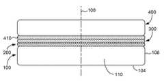
안테나 스위치들과 같은 RF 관련 디바이스를 위한 높은 저항률 반도체-온-절연체(예컨대, 실리콘-온-절연체) 웨이퍼들의 사용은 비용 및 집적화의 관점에서 종래의 기판들에 비해 이점들을 제공한다. 고주파수 응용을 위해 전도성 기판을 사용할 때 고유한 고조파 왜곡을 최소화하고 기생 전력 손실을 감소시키기 위해, 높은 저항률을 갖는 기판 웨이퍼들을 사용하는 것이 필요하지만, 충분하지는 않다. 따라서, RF 디바이스에 대한 핸들 웨이퍼의 저항률은 일반적으로 약 500 Ohm-cm보다 크다. 이제 도 1을 참조하면, 매우 높은 저항률 실리콘 웨이퍼(4), 매립 산화물(BOX) 층(6), 및 실리콘 디바이스 층(10)을 포함하는 실리콘 온 절연체 구조(2)가 있다. 그러한 기판은 자유 캐리어들(전자들 또는 정공들)의 생성을 야기하는 BOX/핸들 계면에서의 높은 전도율 전하 반전 또는 축적 층들(12)을 형성하기 쉽고, 이는 기판의 유효 저항률을 감소시키고 디바이스들이 RF 주파수들에서 작동될 때 기생 전력 손실들 및 디바이스 비선형성을 일으킨다. 이러한 반전/축적 층들은 BOX 고정된 전하, 산화물 트랩된 전하, 계면 트랩된 전하, 및 심지어 디바이스들 자체에 인가된 DC 바이어스로 인한 것일 수 있다.The use of high resistivity semiconductor-on-insulator (eg, silicon-on-insulator) wafers for RF related devices such as antenna switches provides advantages over conventional substrates in terms of cost and integration. In order to minimize the harmonic distortion inherent in using conductive substrates for high frequency applications and to reduce parasitic power losses, it is necessary, but not sufficient, to use substrate wafers with high resistivity. Thus, the resistivity of the handle wafer to the RF device is typically greater than about 500 Ohm-cm. Referring now to FIG. 1 , there is a silicon on
따라서, 심지어 매우 가까운 표면 영역에서도 기판의 높은 저항률이 유지되도록 임의의 유도된 반전 또는 축적 층들에 전하를 트랩(trap)하기 위한 방법이 요구된다. 높은 저항률 핸들 기판과 매립 산화물(BOX) 사이의 전하 트래핑 층(CTL)은 SOI 웨이퍼를 사용하여 제조되는 RF 디바이스의 성능을 개선할 있다는 것이 알려져 있다. 이러한 높은 계면 트랩 층들을 형성하기 위한 다수의 방법들이 제안되었다. 예를 들어, 이제 도 2를 참조하면, RF 디바이스 응용들을 위한 CTL을 갖는 반도체-온-절연체 구조(20)(예컨대, 실리콘-온-절연체, 또는 SOI)를 생성하는 하나의 방법은 높은 저항률을 갖는 실리콘 기판(22) 상에 도핑되지 않은 다결정 실리콘 막(28)을 퇴적하고 그 후 그 위에 산화물(24) 및 상부 실리콘 층(26)의 스택을 형성하는 것에 기초한다. 다결정 실리콘 층(28)은 실리콘 기판(22)과 매립 산화물 층(24) 사이의 높은 결함 층으로서의 역할을 한다. 실리콘-온-절연체 구조(20) 내의 높은 저항률 기판(22)과 매립 산화물 층(24) 사이의 전하 트래핑 층(28)으로서 사용하기 위한 다결정 실리콘 막을 묘사하는 도 2를 참조한다. 대안적인 방법은 가까운 표면 손상 층을 생성하기 위한 중이온(heavy ions)의 주입이다. 무선주파수 디바이스와 같은 디바이스들이 상부 실리콘 층(26) 내에 구축된다.Accordingly, there is a need for a method for trapping charge in any induced inversion or accumulation layers such that a high resistivity of the substrate is maintained even in very close surface areas. It is known that a charge trapping layer (CTL) between a high resistivity handle substrate and a buried oxide (BOX) can improve the performance of RF devices fabricated using SOI wafers. A number of methods have been proposed for forming such high interfacial trap layers. For example, referring now to FIG. 2 , one method of creating a semiconductor-on-insulator structure 20 (eg, silicon-on-insulator, or SOI) with a CTL for RF device applications has a high resistivity. Depositing an undoped
산화물과 기판 사이에서의 다결정 실리콘 층은 디바이스 격리를 개선하고, 송신 라인 손실을 감소시키고, 고조파 왜곡을 감소시킨다는 것이 학술 연구에서 밝혀졌다. 예를 들어, 다음을 참조한다: H. S. Gamble, 외 "Low-loss CPW lines on surface stabilized high resistivity silicon,"Microwave Guided WaveLett., 9(10), pp. 395-397, 1999; D. Lederer, R. Lobet 및 J.-P. Raskin, "Enhanced high resistivity SOI wafers for RF applications,"IEEEIntl.SOIConf., pp. 46-47, 2004; D. Lederer 및 J.-P. Raskin, "New substrate passivation method dedicated to high resistivity SOI wafer fabrication with increased substrate resistivity,"IEEE Electron Device Letters, vol. 26, no. 11, pp.805-807, 2005; D. Lederer, B. Aspar, C.
본 발명은 다층 구조에 관한 것으로, 이 다층 구조는: 단결정 반도체 핸들 기판 - 상기 단결정 반도체 핸들 기판은 대체로 평행한 2개의 주 표면 - 그 중 하나는 상기 단결정 반도체 핸들 기판의 전면이고 그 중 다른 하나는 상기 단결정 반도체 핸들 기판의 후면임 -, 상기 전면과 상기 후면 사이의 가상 중심 평면, 상기 단결정 반도체 핸들 기판의 전면과 후면을 연결하는 둘레 에지, 및 상기 단결정 반도체 핸들 기판의 전면과 후면 사이의 벌크 영역을 포함하고, 상기 단결정 반도체 핸들 기판은 적어도 약 500 ohm-cm의 최소 벌크 영역 저항률을 가짐 -; 다결정 실리콘 층을 포함하는 전하 트래핑 층 - 상기 전하 트래핑 층은 상기 단결정 반도체 핸들 기판의 상기 전면과 계면 접촉하고, 상기 전하 트래핑 층은 적어도 약 1000 ohm-cm의 최소 저항률을 가짐 -; 상기 다결정 실리콘 층과 계면 접촉하는 실리콘 질화물 또는 실리콘 산질화물을 포함하는 절연 층; 및 단결정 실리콘 디바이스 층을 포함한다.The present invention relates to a multilayer structure, the multilayer structure comprising: a single crystal semiconductor handle substrate, the single crystal semiconductor handle substrate having two generally parallel major surfaces, one of which is a front surface of the single crystal semiconductor handle substrate and the other of which is a back surface of the single crystal semiconductor handle substrate, an imaginary center plane between the front and back surfaces, a peripheral edge connecting the front and back surfaces of the single crystal semiconductor handle substrate, and a bulk region between the front and back surfaces of the single crystal semiconductor handle substrate. wherein the single crystal semiconductor handle substrate has a minimum bulk area resistivity of at least about 500 ohm-cm; a charge trapping layer comprising a polycrystalline silicon layer, said charge trapping layer in interfacial contact with said front surface of said single crystal semiconductor handle substrate, said charge trapping layer having a minimum resistivity of at least about 1000 ohm-cm; an insulating layer comprising silicon nitride or silicon oxynitride in interfacial contact with the polycrystalline silicon layer; and a single crystal silicon device layer.
본 발명은 더 추가로 다층 구조를 준비하는 방법에 관한 것으로, 이 방법은: 단결정 반도체 핸들 기판의 전면 상에 전하 트래핑 층을 퇴적하는 단계 - 상기 단결정 반도체 핸들 기판은 대체로 평행한 2개의 주 표면 - 그 중 하나는 상기 단결정 반도체 핸들 기판의 전면이고 그 중 다른 하나는 상기 단결정 반도체 핸들 기판의 후면임 -, 상기 전면과 상기 후면 사이의 가상 중심 평면, 상기 단결정 반도체 핸들 기판의 전면과 후면을 연결하는 둘레 에지, 및 상기 단결정 반도체 핸들 기판의 전면과 후면 사이의 벌크 영역을 포함하고, 상기 단결정 반도체 핸들 기판은 적어도 약 500 ohm-cm의 최소 벌크 영역 저항률을 갖고 또한 상기 전하 트래핑 층은 다결정 실리콘을 포함하고 적어도 약 1000 ohm-cm의 최소 저항률을 가짐 -; 상기 다결정 실리콘 층 상에 실리콘 질화물 또는 실리콘 산질화물을 포함하는 절연 층을 퇴적하는 단계; 및 상기 절연 층에 단결정 반도체 도너 기판의 전면 상의 유전체 층을 접합함으로써 접합된 구조를 형성하는 단계를 포함하고, 상기 단결정 반도체 도너 기판은 대체로 평행한 2개의 주 표면 - 그 중 하나는 상기 반도체 도너 기판의 전면이고 그 중 다른 하나는 상기 반도체 도너 기판의 후면임 -, 상기 반도체 도너 기판의 전면과 후면을 연결하는 둘레 에지, 상기 반도체 도너 기판의 전면과 후면 표면 사이의 중심 평면, 및 상기 반도체 도너 기판의 전면과 후면 사이의 벌크 영역을 포함하고, 또한 상기 단결정 반도체 도너 기판은 벽개면을 포함한다.The present invention still further relates to a method of preparing a multilayer structure, the method comprising: depositing a charge trapping layer on a front surface of a single crystal semiconductor handle substrate, the single crystal semiconductor handle substrate having two generally parallel major surfaces; one of which is the front side of the single crystal semiconductor handle substrate and the other is the back side of the single crystal semiconductor handle substrate - an imaginary center plane between the front side and the back side, connecting the front side and the back side of the single crystal semiconductor handle substrate a peripheral edge and a bulk region between the front and back surfaces of the monocrystalline semiconductor handle substrate, the monocrystalline semiconductor handle substrate having a minimum bulk region resistivity of at least about 500 ohm-cm, and wherein the charge trapping layer comprises polycrystalline silicon. and have a minimum resistivity of at least about 1000 ohm-cm -; depositing an insulating layer comprising silicon nitride or silicon oxynitride on the polycrystalline silicon layer; and forming a bonded structure by bonding a dielectric layer on the front side of a single crystal semiconductor donor substrate to the insulating layer, wherein the single crystal semiconductor donor substrate has two generally parallel major surfaces, one of which is the semiconductor donor substrate. a front surface of and the other of which is the back surface of the semiconductor donor substrate, a peripheral edge connecting the front and back surfaces of the semiconductor donor substrate, a central plane between the front and back surfaces of the semiconductor donor substrate, and the semiconductor donor substrate and a bulk region between the front and back surfaces of the single-crystal semiconductor donor substrate including a cleaved surface.
다른 목적들과 특징들은 부분적으로 명백하고 부분적으로 이하에서 지적될 것이다.Other objects and features will be in part apparent and in part pointed out hereinafter.
도 1은 높은 저항률 기판 및 매립 산화물 층을 포함하는 실리콘-온-절연체 웨이퍼의 묘사이다.
도 2는 종래 기술에 따른 실리콘-온-절연체 웨이퍼의 묘사로서, 이 SOI 웨이퍼는 높은 저항률 기판과 매립 산화물 층 사이의 폴리실리콘 전하 트래핑 층을 포함한다.
도 3a 내지 도 3e는 본 발명의 일부 실시예들에 따른 프로세스 흐름을 묘사한다.
도 4a는 실리콘 질화물 유전체 층을 퇴적하기 위해 질소 플라즈마를 겪는 실리콘 온 절연체 웨이퍼 내의 붕소 농도 프로파일들을 묘사하는 그래프이다. 도 4b는 실리콘 이산화물 유전체 층을 퇴적하기 위해 산소 플라즈마를 겪는 실리콘 온 절연체 웨이퍼 내의 붕소 농도 프로파일들을 묘사하는 그래프이다.
도 5는 CPW 테스트에 의한 2차 고조파 상대 전력을 묘사하는 그래프이다. 이 테스트는 질소 플라즈마 퇴적 및 산소 플라즈마 퇴적에 의해 준비된 웨이퍼들을 비교한다.1 is a depiction of a silicon-on-insulator wafer comprising a high resistivity substrate and a buried oxide layer.
2 is a depiction of a silicon-on-insulator wafer according to the prior art, wherein the SOI wafer includes a polysilicon charge trapping layer between a high resistivity substrate and a buried oxide layer.
3A-3E depict a process flow in accordance with some embodiments of the present invention.
4A is a graph depicting boron concentration profiles in a silicon on insulator wafer that has undergone a nitrogen plasma to deposit a silicon nitride dielectric layer. 4B is a graph depicting boron concentration profiles in a silicon on insulator wafer that has undergone an oxygen plasma to deposit a silicon dioxide dielectric layer.
5 is a graph depicting the second harmonic relative power by the CPW test. This test compares wafers prepared by nitrogen plasma deposition and oxygen plasma deposition.
본 발명에 따르면, 전하 트래핑 층(CTL)을 포함하는 반도체-온-절연체 복합 구조(SOI, 예컨대, 실리콘-온-절연체 복합 구조)를 준비하기 위한 방법이 제공된다. 본 발명은 추가로 반도체-온-절연체 복합 구조(예컨대, 전하 트래핑 층(CTL)을 포함하는 실리콘-온-절연체 복합 구조)에 관한 것이다. 본 개시내용은 무선주파수 디바이스들에서 사용되는 SOI 구조의 전기적 성능을 강화하기 위해 단결정 반도체 핸들 기판을 엔지니어링하는 방법을 제공한다.According to the present invention, a method is provided for preparing a semiconductor-on-insulator composite structure (SOI, eg, silicon-on-insulator composite structure) comprising a charge trapping layer (CTL). The present invention further relates to semiconductor-on-insulator composite structures (eg, silicon-on-insulator composite structures comprising a charge trapping layer (CTL)). The present disclosure provides a method of engineering a single crystal semiconductor handle substrate to enhance the electrical performance of an SOI structure used in radiofrequency devices.
일부 실시예들에서, 본 발명은 완성된 RF 디바이스들의 성능을 상당히 개선하기 위해 다결정 실리콘 전하 트랩 층(CTL)과 도너 기판 사이의 계면을 엔지니어링함으로써 SOI 웨이퍼들을 제조하는 방법에 관한 것이다. 다결정 실리콘 전하 트랩 층(CTL)의 속성은 SOI 구조가 겪는 열 처리에 의존한다. 실제로, SOI 구조 제조 및 디바이스 처리의 열 예산(thermal budget)은 전하 트래핑 층에서 구조적 변화들을 야기할 만큼 충분히 높아서, RF 디바이스 특성들을 개선하기에 효과가 없게 된다. 추가적으로, 접합 계면에서 트랩되는 붕소, 알루미늄, 및 다른 금속들과 같은 오염물질들은 다결정 실리콘 층을 쉽게 관통하여 쉽게 확산되고 다결정 실리콘 층의 저항률을 감소시키거나 다결정 실리콘 층의 재결정화를 유도할 수 있다. 이러한 효과들 중 어느 것이든 RF 성능을 개선하는 데 다결정 실리콘 층의 유효성을 감소시킨다. 본 발명의 목적은 전하 트래핑 유효성을 보존하고 완성된 RF 디바이스의 성능을 상당히 개선하는 열 안정적인 CTL들을 갖는 SOI 웨이퍼를 제조하는 방법을 제공하는 것이다.In some embodiments, the present invention relates to a method of fabricating SOI wafers by engineering the interface between a polycrystalline silicon charge trap layer (CTL) and a donor substrate to significantly improve the performance of finished RF devices. The properties of the polycrystalline silicon charge trap layer (CTL) depend on the thermal treatment that the SOI structure undergoes. In practice, the thermal budget of SOI structure fabrication and device processing is high enough to cause structural changes in the charge trapping layer, making it ineffective to improve RF device characteristics. Additionally, contaminants such as boron, aluminum, and other metals that are trapped at the junction interface can easily penetrate the polysilicon layer and easily diffuse and reduce the resistivity of the polysilicon layer or induce recrystallization of the polysilicon layer. . Either of these effects reduces the effectiveness of the polycrystalline silicon layer in improving RF performance. It is an object of the present invention to provide a method of fabricating an SOI wafer with thermally stable CTLs that preserves charge trapping effectiveness and significantly improves the performance of the finished RF device.
I.반도체 핸들 기판 및 반도체 도너 기판I. Semiconductor handle substrate and semiconductor donor substrate
본 발명에서 사용하기 위한 기판은 반도체 핸들 기판, 예컨대, 단결정 반도체 핸들 웨이퍼 및 반도체 도너 기판, 예컨대 단결정 반도체 도너 웨이퍼를 포함한다. 반도체-온-절연체 복합 구조 내의 반도체 디바이스 층은 단결정 반도체 도너 웨이퍼로부터 도출된다. 반도체 디바이스 층은 반도체 도너 기판을 에칭하는 것과 같은 웨이퍼 씨닝 기법들에 의해 또는 손상 평면을 포함하는 반도체 도너 기판을 벽개함으로써 반도체 핸들 기판 상으로 전이될 수 있다.Substrates for use in the present invention include semiconductor handle substrates, such as single crystal semiconductor handle wafers, and semiconductor donor substrates, such as single crystal semiconductor donor wafers. The semiconductor device layer in the semiconductor-on-insulator composite structure is derived from a single crystal semiconductor donor wafer. The semiconductor device layer may be transferred onto the semiconductor handle substrate by wafer thinning techniques such as etching the semiconductor donor substrate or by cleaving the semiconductor donor substrate containing the damage plane.
도 3a 내지 도 3e는 본 발명의 일부 실시예들에 따른 프로세스 흐름을 묘사한다. 도 3a를 참조하면, 예시적인 비제한적 단결정 반도체 핸들 웨이퍼(100)가 묘사되어 있다. 일반적으로, 단결정 반도체 핸들 웨이퍼(100)는 대체로 평행한 2개의 주 표면을 포함한다. 평행한 표면들 중 하나는 단결정 반도체 핸들 웨이퍼(100)의 전면(102)이고, 다른 평행한 표면은 단결정 반도체 핸들 웨이퍼(100)의 후면(104)이다. 단결정 반도체 핸들 웨이퍼(100)는 전면과 후면(102, 104)을 연결하는 둘레 에지(106)를 포함한다. 단결정 반도체 핸들 웨이퍼(100)는, 대체로 평행한 2개의 주 표면(102, 104)에 수직이고 전면과 후면(102, 104) 사이의 중간 포인트들에 의해 정의되는 중심 평면에도 수직인 중심 축(108)을 포함한다. 단결정 반도체 핸들 웨이퍼(100)는 대체로 평행한 2개의 주 표면(102, 104) 사이에 벌크 영역(110)을 포함한다. 반도체 웨이퍼, 예컨대, 실리콘 웨이퍼는, 전형적으로, 어떤 전체 두께 변동(TTV), 뒤틀림(warp), 및 휨(bow)을 가지므로, 전면(102) 상의 모든 포인트와 후면(104) 상의 모든 포인트 사이의 중간점은 평면 내에 정밀하게 속하지 않을 수 있다. 그러나, 실제적 문제로서, TTV, 뒤틀림, 및 휨은 전형적으로 매우 경미하여 근접한 근사치로 중간점들은 전면과 후면(102, 104) 사이에 대략적으로 등거리에 있는 가상 중심 평면 내에 속한다고 말할 수 있다.3A-3E depict a process flow in accordance with some embodiments of the present invention. Referring to FIG. 3A , an exemplary non-limiting single crystal
본 명세서에 설명된 임의의 동작 전에, 단결정 반도체 핸들 웨이퍼(100)의 전면(102) 및 후면(104)은 실질적으로 동일할 수 있다. 단지 편의를 위해 그리고 일반적으로 본 발명의 방법의 동작들이 수행되는 표면을 구별하기 위하여, 표면은 "전면(front surface)" 또는 "후면(back surface)"으로 지칭된다. 본 발명의 맥락에서, 단결정 반도체 핸들 웨이퍼(100), 예컨대, 단결정 실리콘 핸들 웨이퍼의 "전면"은 접합된 구조의 내부 표면이 되는 기판의 주 표면을 지칭한다. 따라서, 단결정 반도체 핸들 웨이퍼(100), 예컨대, 핸들 웨이퍼의 "후면"은 접합된 구조의 외부 표면이 되는 주 표면을 지칭한다. 유사하게, 단결정 반도체 도너 기판, 예컨대, 단결정 실리콘 도너 웨이퍼의 "전면"은 접합된 구조의 내부 표면이 되는 단결정 반도체 도너 기판의 주 표면을 지칭하고, 단결정 반도체 도너 기판, 예컨대, 단결정 실리콘 도너 웨이퍼의 "후면"은 접합된 구조의 외부 표면이 되는 주 표면을 지칭한다. 본 발명의 맥락에서, 단결정 반도체 핸들 기판(100) 및 단결정 반도체 도너 기판 중 어느 하나 또는 둘 다의 전면들 상에 하나 이상의 절연 층이 준비될 수 있다. 종래의 접합 및 웨이퍼 씨닝 단계들이 완료되면, 단결정 반도체 도너 기판은 반도체-온-절연체(예컨대, 실리콘-온-절연체) 복합 구조의 반도체 디바이스 층을 형성한다.Prior to any operation described herein, the
단결정 반도체 핸들 기판과 단결정 반도체 도너 기판은 단결정 반도체 웨이퍼들일 수 있다. 바람직한 실시예들에서, 반도체 웨이퍼는 실리콘, 실리콘 탄화물, 실리콘 게르마늄, 갈륨 비화물, 갈륨 질화물, 인듐 인화물, 인듐 갈륨 비화물, 게르마늄, 및 이들의 조합들로 구성되는 그룹으로부터 선택된 재료를 포함한다. 본 발명의 단결정 반도체 웨이퍼들, 예컨대, 단결정 실리콘 핸들 웨이퍼 및 단결정 실리콘 도너 웨이퍼는 전형적으로 적어도 약 150 mm, 적어도 약 200 mm, 적어도 약 300 mm, 또는 적어도 약 450 mm의 공칭 직경을 갖는다. 웨이퍼 두께는 약 250 마이크로미터 내지 약 1500 마이크로미터, 예컨대 약 300 마이크로미터 내지 약 1000 마이크로미터, 적합하게는 약 500 마이크로미터 내지 약 1000 마이크로미터의 범위 내에서 변화할 수 있다. 일부 특정 실시예들에서, 웨이퍼 두께는 약 725 마이크로미터일 수 있다. 일부 실시예들에서, 웨이퍼 두께는 약 775 마이크로미터일 수 있다.The single crystal semiconductor handle substrate and the single crystal semiconductor donor substrate may be single crystal semiconductor wafers. In preferred embodiments, the semiconductor wafer comprises a material selected from the group consisting of silicon, silicon carbide, silicon germanium, gallium arsenide, gallium nitride, indium phosphide, indium gallium arsenide, germanium, and combinations thereof. The single crystal semiconductor wafers of the present invention, such as a single crystal silicon handle wafer and a single crystal silicon donor wafer, typically have a nominal diameter of at least about 150 mm, at least about 200 mm, at least about 300 mm, or at least about 450 mm. The wafer thickness may vary within the range of from about 250 micrometers to about 1500 micrometers, such as from about 300 micrometers to about 1000 micrometers, suitably from about 500 micrometers to about 1000 micrometers. In some specific embodiments, the wafer thickness may be about 725 micrometers. In some embodiments, the wafer thickness may be about 775 micrometers.
특히 바람직한 실시예들에서, 단결정 반도체 웨이퍼들은 종래의 초크랄스키(Czochralski) 결정 성장 방법들 또는 플로트 존(float zone) 성장 방법들에 따라 성장된 단결정 잉곳으로부터 슬라이싱된 단결정 실리콘 웨이퍼들을 포함한다. 그러한 방법뿐만 아니라, 표준 실리콘 슬라이싱, 랩핑, 에칭, 및 연마 기법들은, 예를 들어, F. Shimura, Semiconductor Silicon Crystal Technology, Academic Press, 1989, 및 Silicon Chemical Etching, (J. Grabmaier ed.) Springer-Verlag, N.Y., 1982(인용에 의해 본 명세서에 포함됨)에 개시되어 있다. 바람직하게는, 웨이퍼들은 본 기술분야의 통상의 기술자들에게 알려진 표준 방법에 의해 연마되고 세정된다. 예를 들어, 다음을 참조한다: W.C. O'Mara 외,Handbook of Semiconductor Silicon Technology, Noyes Publications. 원한다면, 웨이퍼들은, 예를 들어, 표준 SC1/SC2 용액에서 세정될 수 있다. 일부 실시예들에서, 본 발명의 단결정 실리콘 웨이퍼들은 종래의 초크랄스키("Cz") 결정 성장 방법들에 따라 성장된 단결정 잉곳으로부터 슬라이싱된 단결정 실리콘 웨이퍼들이고, 전형적으로, 적어도 약 150 mm, 적어도 약 200 mm, 적어도 약 300 mm, 또는 적어도 약 450 mm의 공칭 직경을 갖는다. 바람직하게는, 단결정 실리콘 핸들 웨이퍼 및 단결정 실리콘 도너 웨이퍼 둘 다는 표면 결함, 예컨대 스크래치, 큰 입자 등이 없는 미러 연마된 전면 마감을 갖는다. 웨이퍼 두께는 약 250 마이크로미터 내지 약 1500 마이크로미터, 예컨대 약 300 마이크로미터 내지 약 1000 마이크로미터, 적합하게는 약 500 마이크로미터 내지 약 1000 마이크로미터의 범위 내에서 변화할 수 있다. 일부 특정 실시예들에서, 웨이퍼 두께는 약 725 마이크로미터 내지 약 800 마이크로미터, 예컨대 약 750 마이크로미터 내지 약 800 마이크로미터일 수 있다. 일부 실시예들에서, 웨이퍼 두께는 약 725 마이크로미터일 수 있다. 일부 실시예들에서, 웨이퍼 두께는 약 775 마이크로미터일 수 있다.In particularly preferred embodiments, the single crystal semiconductor wafers comprise single crystal silicon wafers sliced from a single crystal ingot grown according to conventional Czochralski crystal growth methods or float zone growth methods. As well as such methods, standard silicon slicing, lapping, etching, and polishing techniques are described, for example, by F. Shimura, Semiconductor Silicon Crystal Technology, Academic Press, 1989, and Silicon Chemical Etching, (J. Grabmaier ed.) Springer- Verlag, NY, 1982 (incorporated herein by reference). Preferably, the wafers are polished and cleaned by standard methods known to those skilled in the art. See, for example: WC O'Mara et al.,Handbook of Semiconductor Silicon Technology , Noyes Publications. If desired, the wafers can be cleaned, for example, in a standard SC1/SC2 solution. In some embodiments, single crystal silicon wafers of the present invention are single crystal silicon wafers sliced from a single crystal ingot grown according to conventional Czochralski ("Cz") crystal growth methods, typically at least about 150 mm, at least have a nominal diameter of about 200 mm, at least about 300 mm, or at least about 450 mm. Preferably, both the single crystal silicon handle wafer and the single crystal silicon donor wafer have a mirror polished front surface finish free of surface defects such as scratches, large particles, etc. The wafer thickness may vary within the range of from about 250 micrometers to about 1500 micrometers, such as from about 300 micrometers to about 1000 micrometers, suitably from about 500 micrometers to about 1000 micrometers. In some specific embodiments, the wafer thickness may be between about 725 micrometers and about 800 micrometers, such as between about 750 micrometers and about 800 micrometers. In some embodiments, the wafer thickness may be about 725 micrometers. In some embodiments, the wafer thickness may be about 775 micrometers.
일부 실시예들에서, 단결정 반도체 웨이퍼들, 즉, 단결정 반도체 핸들 웨이퍼 및 단결정 반도체 도너 웨이퍼는 일반적으로 초크랄스키 성장 방법에 의해 달성되는 농도의 격자간 산소(interstitial oxygen)를 포함한다. 일부 실시예들에서, 단결정 반도체 웨이퍼들은 약 4 PPMA 내지 약 18 PPMA의 농도의 산소를 포함한다. 일부 실시예들에서, 반도체 웨이퍼들은 약 10 PPMA 내지 약 35 PPMA의 농도의 산소를 포함한다. 일부 실시예들에서, 단결정 실리콘 웨이퍼는 약 12 PPMA보다 크지 않은, 예컨대 약 10 PPMA보다 작은 농도의 산소를 포함한다. 격자간 산소는 SEMI MF 1188-1105에 따라 측정될 수 있다.In some embodiments, single crystal semiconductor wafers, ie, single crystal semiconductor handle wafer and single crystal semiconductor donor wafer, contain interstitial oxygen at a concentration generally achieved by the Czochralski growth method. In some embodiments, the single crystal semiconductor wafers include oxygen at a concentration of about 4 PPMA to about 18 PPMA. In some embodiments, the semiconductor wafers include oxygen at a concentration of about 10 PPMA to about 35 PPMA. In some embodiments, the single crystal silicon wafer includes oxygen at a concentration not greater than about 12 PPMA, such as less than about 10 PPMA. Interstitial oxygen can be measured according to SEMI MF 1188-1105.
단결정 반도체 핸들 웨이퍼(100)는 초크랄스키 또는 플로트 존 방법들에 의해 획득될 수 있는 임의의 저항률을 가질 수 있다. 따라서, 단결정 반도체 핸들 웨이퍼(100)의 저항률은 본 발명의 구조의 최종 사용/응용의 요건에 기초한다. 따라서, 저항률은 밀리옴 이하 내지 메가옴 이상으로 변화할 수 있다. 일부 실시예들에서, 단결정 반도체 핸들 웨이퍼(100)는 p형 또는 n형 도펀트를 포함한다. 적합한 도펀트는, 붕소(p형), 갈륨(p형), 인(n형), 안티몬(n형), 및 비소(n형)를 포함한다. 도펀트 농도는 핸들 웨이퍼의 원하는 저항률에 기초하여 선택된다. 일부 실시예들에서, 단결정 반도체 핸들 기판은 p형 도펀트를 포함한다. 일부 실시예들에서, 단결정 반도체 핸들 기판은 붕소와 같은 p형 도펀트를 포함하는 단결정 실리콘 웨이퍼이다.The single crystal
일부 실시예들에서, 단결정 반도체 핸들 웨이퍼(100)는 약 100 ohm-cm 미만, 약 50 ohm-cm 미만, 약 1 ohm-cm 미만, 약 0.1 ohm-cm 미만 또는 심지어 약 0.01 ohm-cm 미만과 같은, 비교적 낮은 최소 벌크 저항률을 갖는다. 일부 실시예들에서, 단결정 반도체 핸들 기판(100)은 약 100 ohm-cm 미만, 또는 약 1 ohm-cm 내지 약 100 ohm-cm와 같은, 비교적 낮은 최소 벌크 저항률을 갖는다. 낮은 저항률 웨이퍼들은 붕소(p형), 갈륨(p형), 알루미늄(p형), 인듐(p형), 인(n형), 안티몬(n형), 및 비소(n형)와 같은 전기적 활성 도펀트들을 포함할 수 있다.In some embodiments, the single crystal
일부 실시예들에서, 단결정 반도체 핸들 웨이퍼(100)는 비교적 높은 최소 벌크 저항률을 갖는다. 높은 저항률 웨이퍼들은 일반적으로 초크랄스키 방법 또는 플로트 존 방법에 의해 성장된 단결정 잉곳으로부터 슬라이싱된다. 높은 저항률 웨이퍼들은, 붕소(p형), 갈륨(p형), 알루미늄(p형), 인듐(p형), 인(n형), 안티몬(n형), 및 비소(n형)와 같은, 전기적 활성 도펀트들을 일반적으로 매우 낮은 농도로 포함할 수 있다. Cz-성장된 실리콘 웨이퍼들은 결정 성장 동안에 혼입되는 산소에 의해 야기된 열 도너(thermal donors)를 전멸시키기 위해 약 600℃ 내지 약 1000℃ 범위의 온도에서 열 어닐링을 겪을 수 있다. 일부 실시예들에서, 단결정 반도체 핸들 웨이퍼는 적어도 100 Ohm-cm, 또는 심지어 적어도 약 500 Ohm-cm의, 예컨대 약 100 Ohm-cm 내지 약 100,000 Ohm-cm, 또는 약 500 Ohm-cm 내지 약 100,000 Ohm-cm, 또는 약 1000 Ohm-cm 내지 약 100,000 Ohm-cm, 또는 약 500 Ohm-cm 내지 약 10,000 Ohm-cm, 또는 약 750 Ohm-cm 내지 약 10,000 Ohm, 약 1000 Ohm-cm 내지 약 10,000 Ohm-cm, 약 1000 Ohm-cm 내지 약 6000 ohm-cm, 약 2000 Ohm-cm 내지 약 10,000 Ohm-cm, 약 3000 Ohm-cm 내지 약 10,000 Ohm-cm, 또는 약 3000 Ohm-cm 내지 약 5,000 Ohm-cm의 최소 벌크 저항률을 갖는다. 일부 바람직한 실시예들에서, 단결정 반도체 핸들 기판은 약 1000 Ohm-cm 내지 약 6,000 Ohm-cm의 벌크 저항률을 갖는다. 높은 저항률 웨이퍼들을 준비하는 방법들은 본 기술분야에 알려져 있고, 그러한 높은 저항률 웨이퍼들은 SunEdison Semiconductor Ltd.(St. Peters, MO; 예전에는 MEMC Electronic Materials, Inc.)와 같은 상업적 공급자들로부터 획득될 수 있다.In some embodiments, the single crystal
일부 바람직한 실시예들에서, 단결정 반도체 핸들 기판은 붕소, 알루미늄, 갈륨, 인듐, 및 이들의 임의의 조합으로 구성되는 그룹으로부터 선택된 전기적 활성 도펀트를 포함한다. 일부 바람직한 실시예들에서, 단결정 반도체 핸들 기판은 약 2x10¹³ atoms/cm3보다 작은, 약 1x10¹³ atoms/cm3보다 작은, 예컨대 약 5x10¹² atoms/cm3보다 작은, 또는 약 1x10¹² atoms/cm3보다 작은 농도로 존재할 수 있는, 붕소를 포함한다. 높은 저항률 웨이퍼들을 준비하는 방법들은 본 기술분야에 알려져 있고, 그러한 높은 저항률 웨이퍼들은 SunEdison Semiconductor Ltd.(St. Peters, MO; 예전에는 MEMC Electronic Materials, Inc.)와 같은 상업적 공급자들로부터 획득될 수 있다.In some preferred embodiments, the single crystal semiconductor handle substrate comprises an electrically active dopant selected from the group consisting of boron, aluminum, gallium, indium, and any combination thereof. In some preferred embodiments, the single crystal semiconductor handle substrate isless than about 2x10 13 atoms/cm3 , less than about 1x10¹³ atoms/cm3 , such as less than about 5x10¹² atoms/cm3 , or about 1x10¹² atoms/cm boron, which may be present in concentrations less than3; Methods for preparing high resistivity wafers are known in the art, and such high resistivity wafers can be obtained from commercial suppliers such as SunEdison Semiconductor Ltd. (St. Peters, MO; formerly MEMC Electronic Materials, Inc.). .
단결정 반도체 핸들 웨이퍼(100)는 단결정 실리콘을 포함할 수 있다. 단결정 반도체 핸들 웨이퍼(100)는, 예를 들어, (100), (110), 또는 (111) 결정 배향 중 임의의 결정 배향을 가질 수 있고, 결정 배향의 선택은 구조의 최종 사용에 의해 좌우될 수 있다.The single crystal
옵션으로, 전면(102), 후면(104), 또는 둘 다는 본 기술분야에 알려진 방법들에 따라 산화될 수 있다. 산화는 열 산화(퇴적된 반도체 재료 막의 일부 부분이 소모될 것임) 또는 CVD 산화물 퇴적과 같은, 본 기술분야에 알려진 수단에 의해 완수될 수 있다. 전면(102), 후면(104) 또는 둘 다 상의 산화 층은 적어도 약 1 나노미터 두께, 예컨대 약 10 나노미터 내지 약 5000 나노미터 두께, 예컨대 약 100 나노미터 내지 약 1000 나노미터, 또는 약 200 나노미터 내지 약 400 나노미터일 수 있다. 일부 실시예들에서, 산화 층은 예컨대 약 5 옹스트롬 내지 약 25 옹스트롬, 예컨대 약 10 옹스트롬 내지 약 15 옹스트롬으로, 비교적 얇다. 얇은 산화물 층들은 SC1/SC2 세정 용액과 같은 표준 세정 용액에의 노출에 의해 획득될 수 있다. 일부 실시예들에서, SC1 용액은, 5부(5 parts)의 탈이온수, 1부(1 part)의 수성 NH4OH(수산화암모늄, 29 중량%의 NH3), 및 1부의 수성 H2O2(과산화수소, 30%)를 포함한다. 일부 실시예들에서, 핸들 기판은, SC2 용액과 같은, 산화제를 포함하는 수용액에 노출시킴으로써 산화될 수 있다. 일부 실시예들에서, SC2 용액은 5부의 탈이온수, 1부의 수성 HCl(염산, 39 중량%), 및 1부의 수성 H2O2(과산화수소, 30%)를 포함한다.Optionally, the
II.전하 트래핑 층의 퇴적II. Deposition of the charge trapping layer
본 발명의 방법에 따르면 그리고 도 3a 및 도 3b를 참조하면, 전하 트래핑 층(200)이 단결정 반도체 핸들 웨이퍼(100)의 전면(102)과 접촉하여 퇴적된다. 일부 실시예들에서, 전하 트래핑 층(200)은 다결정 실리콘을 포함한다. 그러한 재료들은 다결정 반도체 재료들 및 비정질 반도체 재료들을 포함한다. 다결정 또는 비정질일 수 있는 재료들은 실리콘(Si), 실리콘 게르마늄(SiGe), 탄소가 도핑된 실리콘(SiC), 및 게르마늄(Ge)을 포함한다. 다결정 반도체, 예컨대, 다결정 실리콘은, 랜덤 결정 배향들을 갖는 작은 실리콘 결정들을 포함하는 재료를 나타낸다. 다결정 재료는 랜덤 결정 배향들을 갖는 작은 결정들을 포함하는 재료를 나타낸다. 다결정 입자들은 크기가 약 20 나노미터만큼 작을 수 있고, 입자 크기는 일반적으로 약 20 나노미터 내지 약 1 마이크로미터, 예컨대 약 0.3 마이크로미터 내지 약 1 마이크로미터의 범위이다. 본 발명의 방법에 따르면, 퇴적된 다결정 재료의 결정 입자 크기가 더 작을수록 전하 트래핑 층에서의 결함은 더 높아진다. 다결정 실리콘 전하 트래핑 층의 저항률은 적어도 100 Ohm-cm, 적어도 약 500 Ohm-cm, 적어도 약 1000 Ohm-cm, 적어도 약 3000 Ohm-cm, 또는 심지어 적어도 약 7000 Ohm-cm, 예컨대 약 100 Ohm-cm 내지 약 100,000 Ohm-cm, 또는 약 500 Ohm-cm 내지 약 100,000 Ohm-cm, 또는 약 1000 Ohm-cm 내지 약 100,000 Ohm-cm, 또는 약 500 Ohm-cm 내지 약 100,000 Ohm-cm, 또는 약 750 Ohm-cm 내지 약 100,000 Ohm-cm일 수 있다. 일부 바람직한 실시예들에서, 다결정 실리콘 층의 저항률은 약 3000 Ohm-cm 내지 약 100,000 Ohm-cm, 예컨대 약 3000 Ohm-cm 내지 약 10,000 Ohm-cm 또는 심지어 약 7000 Ohm-cm 내지 약 100,000 ohm-cm, 예컨대 약 7000 ohm-cm 내지 약 10,000 ohm-cm이다.In accordance with the method of the present invention and referring to FIGS. 3A and 3B , a
단결정 반도체 핸들 웨이퍼(100)의 전면(102) 상의 전하 트래핑 층(200)의 퇴적을 위한 재료는 기상 증착에 의해 퇴적될 수 있다. 전하 트래핑 층(200)의 퇴적을 위한 재료는 화학 또는 물리 기상 증착에 의해, 예를 들어, 금속유기 화학 기상 증착(MOCVD), 물리 기상 증착(PVD), 화학 기상 증착(CVD), 저압 화학 기상 증착(LPCVD), 또는 플라즈마 강화 화학 기상 증착(PECVD)에 의해 퇴적될 수 있다. 바람직한 실시예들에서, 다결정 실리콘은 CVD에 의해 퇴적된다. CVD를 위한 실리콘 프리커서들은, 여러 가지 중에서도, 메틸 실란, 실리콘 테트라하이드라이드(실란), 트리실란, 디실란, 펜타실란, 네오펜타실란, 테트라실란, 디클로로실란(SiH2Cl2), 트리클로로실란(SiHCl3), 실리콘 테트라클로라이드(SiCl4)를 포함한다. 일부 바람직한 실시예들에서, 실리콘 프리커서는 실란, 디클로로실란(SiH2Cl2), 및 트리클로로실란(SiHCl3) 중에서 선택된다. 예를 들어, 다결정 실리콘은 약 850℃보다 큰, 예컨대 약 850℃ 내지 약 1100℃, 또는 약 850℃ 내지 약 1000℃의 온도에서 실란, 디클로로실란(SiH2Cl2), 및 트리클로로실란(SiHCl3)의 CVD에 의해 표면 산화 층 상에 퇴적될 수 있다. 높은 온도는, 여러 이점들 중에서도, 높은 성장 속도에 기여함으로써, 스루풋 및 비용 감소에 기여한다. CVD 퇴적 속도는 적어도 약 0.1 마이크로미터/분, 예컨대 약 0.1 마이크로미터/분 내지 약 10 마이크로미터/분, 또는 약 0.1 마이크로미터/분 내지 약 2 마이크로미터/분의 범위일 수 있다. 다결정 실리콘 층의 퇴적은 층이 적어도 약 0.1 마이크로미터, 예컨대 약 0.1 마이크로미터 내지 약 50 마이크로미터, 예컨대 약 0.1 마이크로미터 내지 약 20 마이크로미터, 약 0.1 마이크로미터 내지 약 10 마이크로미터, 약 0.5 마이크로미터 내지 약 5 마이크로미터, 또는 약 0.5 마이크로미터 내지 약 3 마이크로미터, 예컨대 약 1 마이크로미터 내지 약 2 마이크로미터 또는 약 2 마이크로미터 내지 약 5 마이크로미터의 두께를 가질 때까지 계속될 수 있다. 퇴적은 약 1 Torr 내지 약 760 Torr, 예컨대 약 1 Torr 내지 약 400 Torr의 압력에서 발생할 수 있다.The material for the deposition of the
일부 실시예들에서, 화학 기상 증착에 의한 다결정 실리콘 층의 퇴적은 다결정 실리콘 시드 층의 퇴적 후에 중단된다. 다결정 실리콘 시드 층은 최종 다결정 실리콘 전하 트래핑 층의 원하는 전체 두께보다 작은 두께를 가질 수 있다. 따라서, 다결정 시드 층은 20 마이크로미터보다 작은, 10 마이크로미터보다 작은, 5 마이크로미터보다 작은, 3 마이크로미터보다 작은, 2 마이크로미터보다 작은, 또는 1 마이크로미터보다 작은, 또는 0.5 마이크로미터보다 작은, 예컨대 약 50 나노미터 내지 약 20 마이크로미터, 또는 약 50 나노미터 내지 약 10 마이크로미터, 또는 약 50 나노미터 내지 약 5 마이크로미터, 또는 약 50 나노미터 내지 약 3 마이크로미터, 또는 약 50 나노미터 내지 약 2 마이크로미터, 또는 약 50 나노미터 내지 약 1 마이크로미터, 또는 약 50 나노미터 내지 약 500 나노미터, 또는 약 50 나노미터 내지 약 200 나노미터의 두께로 퇴적될 수 있다. 시드 층의 두께는 폴리실리콘 핵의 크기에 의해 설정된다. 효과적인 응력 해제를 달성하기 위해, 시드 층은 50nm보다 작은 보이드들을 남기면서 하부 층의 표면을 커버할 필요가 있고, 이는 폴리실리콘 시드 층과 하부 층 사이의 계면으로의 H2의 액세스를 가능하게 한다. H2는 계면 산화물을 감소시키고, 폴리실리콘 시드 층의 입자 경계들에서의 원자들의 기판으로의 확산을 촉진하고, 따라서 막 응력을 해제한다. 시드 층이 하부 층으로의 H2 액세스를 완전히 방지할 만큼 충분히 두꺼울 때, 후속 어닐링 프로세스는 막 응력을 효과적으로 해제할 수 없다. 다른 한편, 시드 층이 연속적이지 않고 2개의 인접한 핵 사이의 개구 면적이 50 nm보다 넓은 경우, 시드 어닐링 프로세스 동안 큰 핵들이 형성된다. 큰 핵들은 폴리실리콘 퇴적의 끝에서 큰 입자들(즉, 직경 > 1um)로 성장할 것이고, 이는 트래핑 효율을 감소시킨다. 퇴적은 CVD 챔버 내로의 실리콘 프리커서들의 흐름을 중지시킴으로써 중단될 수 있다. 다결정 실리콘의 퇴적의 중단 후에, 다결정 시드 층을 포함하는 핸들 기판이 어닐링될 수 있다. 다결정 시드 층을 어닐링하는 것은 깨끗한 표면, 고순도 막, 높은 저항률 막, 원하는 핵 크기 및 균일성, 및 잔여 막 응력의 감소의 획득과 같은, 바람직한 전하 트래핑 층 속성들에 기여한다. 일부 실시예들에서, 다결정 실리콘 시드 층은 막 응력을 약 0 MPa 내지 약 500 MPa, 예컨대 약 0 MPa 내지 약 100 MPa의 범위로 감소시키기 위해 고온 어닐링을 겪는다. 다결정 시드 층은 약 1000℃보다 큰, 예컨대 약 1000℃ 내지 약 1200℃, 또는 약 1000℃ 내지 약 1100℃의 온도에서 어닐링된다. 시드 층은 약 1초 내지 약 300초, 예컨대 약 5초 내지 약 60초, 또는 약 10초 내지 약 40초의 지속기간 동안 어닐링될 수 있다. 어닐링을 위한 분위기 대기는 수소, 염화수소, 염소, 또는 수소, 염화수소, 및 염소의 임의의 조합을 포함할 수 있다. 어닐링 단계는 감소된 압력 또는 대기압에서, 예컨대 약 1 Torr 내지 약 760 Torr, 또는 약 10 Torr 내지 약 760 Torr에서 수행될 수 있다. 다결정 실리콘 막의 응력 및 입자 크기는 어닐링 온도, 지속기간, 및 가스 흐름에 의해 제어된다. 적절한 어닐링 지속기간 후에, 다결정 실리콘 층의 화학 기상 증착에 의한 퇴적은 단결정 반도체 핸들 기판을 약 850℃ 내지 약 1000℃의 온도로 냉각한 후에 재개된다.In some embodiments, deposition of the polycrystalline silicon layer by chemical vapor deposition is stopped after deposition of the polycrystalline silicon seed layer. The polycrystalline silicon seed layer may have a thickness that is less than the overall desired thickness of the final polycrystalline silicon charge trapping layer. Thus, the polycrystalline seed layer is smaller than 20 micrometers, smaller than 10 micrometers, smaller than 5 micrometers, smaller than 3 micrometers, smaller than 2 micrometers, or smaller than 1 micrometer, or smaller than 0.5 micrometers; such as from about 50 nanometers to about 20 micrometers, or from about 50 nanometers to about 10 micrometers, or from about 50 nanometers to about 5 micrometers, or from about 50 nanometers to about 3 micrometers, or from about 50 nanometers to about 3 micrometers. It may be deposited to a thickness of about 2 micrometers, or about 50 nanometers to about 1 micrometer, or about 50 nanometers to about 500 nanometers, or about 50 nanometers to about 200 nanometers. The thickness of the seed layer is set by the size of the polysilicon nucleus. To achieve effective stress release, the seed layer needs to cover the surface of the underlying layer leaving voids smaller than 50 nm, which enables accessof H 2 to the interface between the polysilicon seed layer and the underlying layer. . H2 reduces interfacial oxide and promotes diffusion of atoms at grain boundaries of the polysilicon seed layer into the substrate, thus releasing film stress. When the seed layer isthick enough to completely prevent H 2 access to the underlying layer, the subsequent annealing process cannot effectively release the film stress. On the other hand, if the seed layer is not continuous and the opening area between two adjacent nuclei is larger than 50 nm, large nuclei are formed during the seed annealing process. Large nuclei will grow into large particles (ie, diameter > 1 um) at the end of polysilicon deposition, which reduces trapping efficiency. Deposition can be stopped by stopping the flow of silicon precursors into the CVD chamber. After cessation of deposition of polycrystalline silicon, the handle substrate including the polycrystalline seed layer may be annealed. Annealing the polycrystalline seed layer contributes to desirable charge trapping layer properties, such as obtaining a clean surface, high purity film, high resistivity film, desired nuclei size and uniformity, and reduction of residual film stress. In some embodiments, the polycrystalline silicon seed layer is subjected to a high temperature annealing to reduce the film stress to a range from about 0 MPa to about 500 MPa, such as from about 0 MPa to about 100 MPa. The polycrystalline seed layer is annealed at a temperature greater than about 1000°C, such as from about 1000°C to about 1200°C, or from about 1000°C to about 1100°C. The seed layer may be annealed for a duration of from about 1 second to about 300 seconds, such as from about 5 seconds to about 60 seconds, or from about 10 seconds to about 40 seconds. The atmospheric atmosphere for the annealing may include hydrogen, hydrogen chloride, chlorine, or any combination of hydrogen, hydrogen chloride, and chlorine. The annealing step may be performed at reduced pressure or atmospheric pressure, such as from about 1 Torr to about 760 Torr, or from about 10 Torr to about 760 Torr. The stress and grain size of the polycrystalline silicon film is controlled by the annealing temperature, duration, and gas flow. After a suitable anneal duration, deposition by chemical vapor deposition of the polycrystalline silicon layer resumes after cooling the single crystal semiconductor handle substrate to a temperature between about 850° C. and about 1000° C.
일부 실시예들에서, 단결정 반도체 핸들 기판(100) 및 다결정 실리콘 전하 트래핑 층(200)은 퇴적이 완료된 후에 어닐링된다. 다결정 시드 층을 어닐링하는 것은 깨끗한 표면, 고순도 막, 높은 저항률 막, 원하는 핵 크기 및 균일성, 및 잔여 막 응력의 감소의 획득과 같은, 바람직한 전하 트래핑 층 속성들에 기여한다. 일부 실시예들에서, 완전히 퇴적된 다결정 실리콘 전하 트래핑 층은 막 응력을 약 0 MPa 내지 약 500 MPa, 예컨대 약 0 MPa 내지 약 100 MPa의 범위로 감소시키기 위해 고온 어닐링을 겪는다. 단결정 반도체 핸들 기판(100) 및 다결정 실리콘 전하 트래핑 층(200)은 약 1000℃보다 큰, 예컨대 약 1000℃ 내지 약 1100℃의 온도에서 어닐링될 수 있다. 단결정 반도체 핸들 기판(100) 및 다결정 실리콘 전하 트래핑 층(200)은 약 1초 내지 약 300초, 예컨대 약 5초 내지 약 60초, 또는 약 10초 내지 약 40초의 지속기간 동안 어닐링될 수 있다. 어닐링을 위한 분위기 대기는 수소, 염화수소, 염소, 또는 수소, 염화수소, 및 염소의 임의의 조합을 포함할 수 있다. 적절한 어닐링 지속기간 후에, CVD 챔버는 단결정 반도체 핸들 기판의 제거를 위해 안전한 온도로 냉각될 수 있다.In some embodiments, the single crystal
전하 트래핑 층(200)의 퇴적 후에, 웨이퍼 세정 및 연마는 옵션이다. 일부 실시예들에서, 퇴적된 다결정 실리콘 전하 트래핑 층은 50 나노미터 정도로 RMS2x2 um2에 의해 측정된 바와 같은 표면 조도를 갖는다. 원한다면, 웨이퍼들은, 예를 들어, 표준 SC1/SC2 용액에서 세정될 수 있다. 추가적으로, 웨이퍼들, 특히, 전하 트래핑 층 상의 옵션의 실리콘 이산화물 층은 표면 조도를 감소시키기 위해 화학 기계적 연마(CMP)를 겪을 수 있고, 표면 조도는, 바람직하게는 RMS2x2um2의 레벨까지 약 5 옹스트롬보다 작고, 예컨대 약 1 옹스트롬 내지 약 2 옹스트롬이고, 여기서 제곱 평균 제곱근(root mean squared) -
III.절연 층의 퇴적III. deposition of an insulating layer
일부 실시예들에서, 그리고 도 3b 및 도 3c를 참조하면, 반도체 질화물 층(예컨대, 실리콘 질화물) 또는 반도체 산질화물 층(예컨대, 실리콘 산질화물)을 포함하는 절연 층(300)이 퇴적된 전하 트래핑 층(200)과 접촉하여 형성될 수 있다. 이것은 열 질화 또는 CVD 질화물 퇴적과 같은 방법들에 의해 완수될 수 있다. 일부 실시예들에서, 전하 트래핑 층은 열 질화될 수 있거나(퇴적된 반도체 재료 막의 일부 부분이 소모될 것임) 또는 막은 CVD 질화물 퇴적에 의해 성장될 수 있다. 일부 실시예들에서, 전하 트래핑 층은 ASM A400과 같은 퍼니스에서 열 질화될 수 있다. 온도는 질화 분위기에서 750℃ 내지 1400℃, 예컨대 1100℃ 내지 1400℃의 범위일 수 있다. 질화 분위기 대기는 Ar, 및 N2 및, 옵션으로, O2와 같은 불활성 가스의 혼합물일 수 있다. 질소 함량은 1 내지 10 퍼센트 또는 더 높게 변화할 수 있다. 예시적인 실시예에서, 반도체 핸들 웨이퍼들은 A400과 같은 수직 퍼니스 내로 로딩될 수 있다. 온도는 Ar 및 N2 및 옵션으로 O2의 혼합물과 함께 질화 온도로 증가된다. 원하는 실리콘 질화물 또는 실리콘 산질화물 두께가 획득된 후에, 가스 흐름은 턴 오프되고, 퍼니스 온도는 감소되고, 웨이퍼들은 퍼니스로부터 언로딩된다. 대안적인 질소 소스는 암모니아이다. 일부 실시예들에서, 전하 트래핑 층은 약 1.5 나노미터 내지 약 50 나노미터 옹스트롬 두께, 예컨대 약 2.5 나노미터 내지 약 10 나노미터 두께, 또는 약 2.5 나노미터 내지 약 5 나노미터 두께, 예컨대 약 3.5 나노미터 두께의 질화물 층 또는 산질화물 층을 제공하기에 충분한 지속기간 동안 처리될 수 있다.In some embodiments, and with reference to FIGS. 3B and 3C , an insulating
일부 실시예들에서, 반도체 질화물 층(예컨대, 실리콘 질화물) 또는 반도체 산질화물 층(예컨대, 실리콘 산질화물)을 포함하는 절연 층(300)은 플라즈마 강화 화학 기상 증착과 같은 CVD에 의해 형성될 수 있다. 일부 실시예들에서, 플라즈마 퇴적 장비는, EVG®810LT 저온 플라즈마 활성화 시스템과 같은, EV 그룹으로부터 이용가능한 것들과 같은, 상업적으로 이용가능한 장비이다. 플라즈마 강화 CVD 챔버의 일반적인 요건은, 다양한 전극 설계, 전력 생성 전자회로, 전력을 가스 부하에 전달하기 위한 임피던스 정합 네트워크, 입력 가스를 위한 질량 흐름 제어기, 및 압력 제어 시스템을 갖춘 반응기를 포함한다. 전형적인 시스템들은 유도 결합된 RF 소스에 의해 전력을 공급받은 수직 튜브 반응기이다. 단결정 반도체 핸들 기판(100)은 챔버 내로 로딩되고 가열된 지지 챔버 상에 배치된다. 챔버는 배기되고 대기압보다 작은 압력까지 아르곤과 같은 캐리어 가스 내의 질소 가스 소스로 다시 채워짐으로써 플라즈마를 생성한다. 암모니아 및/또는 질소 및/또는 일산화 질소(NO) 및/또는 아산화 질소(N2O) 가스는 플라즈마 질화물 처리에 적합한 소스 가스들이다. 산질화물 막들은 산소 및 질소 가스 소스들을 포함시킴으로써 퇴적될 수 있다. 산소 및/또는 물은 플라즈마 산화물 처리를 위한 적합한 소스 가스들이다. 추가적으로, 일산화 질소 또는 아산화 질소의 사용은 절연 층에 산소를 추가적으로 혼입함으로써, 산질화물 막을 퇴적한다. 실리콘 질화물 또는 실리콘 산질화물 플라즈마 막을 퇴적하기 위해, 적합한 실리콘 프리커서들은, 여러 가지 중에서도, 메틸 실란, 실리콘 테트라하이드라이드(실란), 트리실란, 디실란, 펜타실란, 네오펜타실란, 테트라실란, 디클로로실란(SiH2Cl2), 트리클로로실란(SiHCl3), 실리콘 테트라클로라이드(SiCl4)를 포함한다. 적합하게는, Ar이 캐리어 가스로서 추가된다.In some embodiments, the insulating
플라즈마 퇴적은 반도체 질화물(예컨대, 실리콘 질화물) 또는 반도체 산질화물(예컨대, 실리콘 산질화물)의 속성들을 튜닝하도록 변화될 수 있다. 예를 들어, 프리커서들의 압력, 유속, 온도, 및 상대적 비는 플라즈마 퇴적된 질화물 층의 실리콘 및 질화물 몰비들을 튜닝할 수 있다. 추가적으로, 산소 프리커서의 포함은 산소를 혼입하여 산질화물 층을 준비한다. 일부 실시예들에서, 핸들 기판 및/또는 도너 기판 상에 실리콘 질화물 층을 퇴적하기 위해 실리콘 및 질소 프리커서들을 포함하는 분위기 대기에서 플라즈마 퇴적이 발생할 수 있다. 질화물을 퇴적하기에 충분한 지속기간 후에, 산소 프리커서가 대기 내로 도입됨으로써 산질화물을 퇴적할 수 있다. 핸들 반도체 산질화물 층 내의 산소 농도는 기울기에 따라 변화할 수 있고, 그에 의해 산소 농도는 핸들 반도체 질화물 층과의 계면에서 낮고, 핸들 반도체 산질화물 층의 표면을 향해 수직 방향으로 증가한다. 산질화물 층을 퇴적하기에 충분한 지속기간 후에, 질소 프리커서의 흐름이 중지될 수 있고, 퇴적은 실리콘 프리커서 및 산소 가스 소스로만 계속됨으로써 반도체 산화물, 예컨대, 실리콘 산화물을 포함하는 절연 층을 퇴적할 수 있다. 일부 실시예들에서, 절연 층(300)은 반도체 질화물(예컨대, 실리콘 질화물) 층 및 반도체 산질화물(예컨대, 실리콘 산질화물) 층을 포함하는 플라즈마 기법들에 의해 퇴적될 수 있다. 일부 실시예들에서, 절연 층(300)은 반도체 질화물(예컨대, 실리콘 질화물) 층, 반도체 산질화물(예컨대, 실리콘 산질화물) 층, 및 반도체 산화물(예컨대, 실리콘 산화물) 층을 포함하는 플라즈마 기법들에 의해 퇴적될 수 있다. 유리하게, 다수의 절연 층들의 플라즈마 퇴적은 프로세스 가스들의 비들 및 아이덴티티들을 변화시킴으로써, 연속적으로, 즉, 중단 없이 발생할 수 있다.Plasma deposition can be varied to tune properties of a semiconductor nitride (eg, silicon nitride) or a semiconductor oxynitride (eg, silicon oxynitride). For example, the pressure, flow rate, temperature, and relative ratio of the precursors can tune the silicon and nitride molar ratios of the plasma deposited nitride layer. Additionally, the inclusion of an oxygen precursor prepares the oxynitride layer by incorporating oxygen. In some embodiments, plasma deposition may occur in an ambient atmosphere containing silicon and nitrogen precursors to deposit a silicon nitride layer on the handle substrate and/or the donor substrate. After a duration sufficient to deposit the nitride, an oxygen precursor may be introduced into the atmosphere to deposit the oxynitride. The oxygen concentration in the handle semiconductor oxynitride layer can change with a gradient, whereby the oxygen concentration is low at the interface with the handle semiconductor nitride layer and increases in a vertical direction towards the surface of the handle semiconductor oxynitride layer. After a duration sufficient to deposit the oxynitride layer, the flow of the nitrogen precursor may be stopped, and the deposition may continue only with the silicon precursor and the oxygen gas source to deposit an insulating layer comprising a semiconductor oxide, such as silicon oxide. can In some embodiments, the insulating
플라즈마 퇴적된 반도체 질화물(예컨대, 실리콘 질화물) 또는 반도체 산질화물(예컨대, 실리콘 산질화물)은 약 0.01 Torr 내지 약 100 Torr, 예컨대 약 0.1 Torr 내지 약 1 Torr의 압력들에서 형성될 수 있다. 플라즈마 퇴적은 약 20℃ 내지 약 400℃의 온도에서 발생할 수 있다. 약 500 옹스트롬 내지 약 10,000 옹스트롬, 예컨대 약 2000 옹스트롬 내지 약 10,000 옹스트롬의 두께를 갖는 절연 층들이 약 100 옹스트롬/분 내지 약 1000 옹스트롬/분의 속도로 PECVD에 의해 퇴적될 수 있다. The plasma deposited semiconductor nitride (eg, silicon nitride) or semiconductor oxynitride (eg, silicon oxynitride) may be formed at pressures from about 0.01 Torr to about 100 Torr, such as from about 0.1 Torr to about 1 Torr. Plasma deposition may occur at a temperature of about 20°C to about 400°C. Insulating layers having a thickness of from about 500 angstroms to about 10,000 angstroms, such as from about 2000 angstroms to about 10,000 angstroms, may be deposited by PECVD at a rate of from about 100 angstroms/min to about 1000 angstroms/min.
가스 실리콘 프리커서 및 가스 질소 프리커서의 유속 비들은 약 1/200 내지 약 1/50, 예컨대 약 1/100일 수 있다. 이러한 비들은 약 0.7 내지 약 1.8의 실리콘 대 질화물의 몰비를 갖는 실리콘 질화물 층을 산출할 수 있다. 산소 또는 NO와 같은 산소 함유 종들을 추가함으로써 플라즈마 프로세스에 산소가 혼입될 수 있다. 플라즈마 퇴적 동안 산소를 추가하는 것은 기울기 방식으로 변화하는 조성들을 갖는 절연성의 퇴적을 가능하게 하고, 예컨대, 층은 반도체 질화물(예컨대, 실리콘 질화물)로부터 반도체 산화물(예컨대, 실리콘 산화물)에 대한 증가하는 산소 농도의 반도체 산질화물(예컨대, 실리콘 산질화물)로 전이할 수 있다.The flow rate ratios of the gaseous silicon precursor and the gaseous nitrogen precursor may be from about 1/200 to about 1/50, such as about 1/100. Such ratios may yield a silicon nitride layer having a silicon to nitride molar ratio of about 0.7 to about 1.8. Oxygen can be incorporated into the plasma process by adding oxygen or oxygen containing species such as NO. Adding oxygen during plasma deposition allows for the deposition of insulating properties with compositions that change in a gradient manner, for example, the layer increases oxygen from semiconductor nitride (eg, silicon nitride) to semiconductor oxide (eg, silicon oxide). concentration of semiconductor oxynitride (eg, silicon oxynitride).
절연 층들의 굴절률은 1.5 내지 2의 범위에서 튜닝될 수 있다. 막의 접합 계면 또는 수소 함량을 더 튜닝하기 위해 실리콘 산화물, SiO2의 후처리 어닐링 및 화학 기상 증착이 가능하다. 핸들 기판과 도너 기판 사이의 접합은 2 마이크로미터 x 2 마이크로미터 표면 면적에 걸친 제곱 평균 제곱근 방법, RMS2x2um2에 따라 약 5 옹스트롬보다 작은 조도로부터 이익을 얻는다. 일반적으로 이것은 바이어스 전력을 조면화 임계치 아래로 저하시키고 제어된 유도 결합된 플라즈마를 갖는 플라즈마 퇴적에서 달성될 수 있다. 성공적인 층 전이는 약 5 옹스트롬 이하의 조도를 갖는 플라즈마 퇴적된 막들 상에서 예증되었다.The refractive index of the insulating layers can be tuned in the range of 1.5 to 2. Post-treatment annealing and chemical vapor deposition ofsilicon oxide, SiO 2 and chemical vapor deposition are possible to further tune the bonding interface or hydrogen content of the film. The junction between the handle substrate and the donor substrate benefits from a roughness less than about 5 angstroms according to theroot mean square method, RMS 2x2um2 over a 2 micrometer x 2 micrometer surface area. In general this can be achieved in plasma deposition with a controlled inductively coupled plasma by lowering the bias power below the roughening threshold. Successful layer transition has been demonstrated on plasma deposited films with roughness of about 5 angstroms or less.
플라즈마로부터 생성된 실리콘 질화물은 종래의 화학 또는 물리 기상 증착 기법들에 따라 퇴적된 실리콘 질화물과는 구조적으로 다르다. 종래의 CVD 또는 PVD 퇴적은 일반적으로 Si3N4의 화학량론을 갖는 실리콘 질화물 층을 야기한다. 플라즈마 프로세스들은, 입력 반응물 가스들의 비, 전력 레벨, 기판 온도, 및 전체 반응기 압력에 따라 SixNyHz와 같은 조성을 갖는 막을 퇴적하도록 제어될 수 있다. 플라즈마 시스템 내의 경로들은, Si-N, Si=N 및 Si≡N 결합들을 형성하기 위해 존재한다. 이는 플라즈마 에너지가 SixHz 및 NyHz 종들을 생성한다는 사실에 기인한다. 예를 들어, 굴절률과 광학적 갭은 Si/N 비에 따라 극적으로 변화한다. 더 높은 실란 농도에서, 막들은 Si가 풍부하게 되고(LPCVD의 경우 2에 비해) 3.0까지의 굴절률에 도달할 수 있다. 영향을 받을 수 있는 다른 속성들은 유전 상수, 브레이크다운, 기계적, 및 화학적(에칭 레이트)을 포함한다.Silicon nitride produced from plasma is structurally different from silicon nitride deposited according to conventional chemical or physical vapor deposition techniques. Conventional CVD or PVD deposition generally results in a silicon nitride layer with a stoichiometryof Si 3 N4 . Plasma processes can be controlled to deposit a film having a composition such asSi x Ny Hz depending on the ratio of input reactant gases, power level, substrate temperature, and total reactor pressure. Paths in the plasma system exist to form Si-N, Si=N and Si≡N bonds. This is due to the fact that the plasma energy produces Six Hz and Ny Hz species. For example, the refractive index and the optical gap change dramatically with the Si/N ratio. At higher silane concentrations, the films become Si-enriched (compared to 2 for LPCVD) and can reach refractive indices of up to 3.0. Other properties that may be affected include dielectric constant, breakdown, mechanical, and chemical (etch rate).
IV.플라즈마 활성화IV. Plasma activation
일부 실시예들에서, 다결정 실리콘 전하 트래핑 층(200) 및 절연 층(300)을 포함하는 단결정 반도체 핸들 기판(100)은 산소 플라즈마 및/또는 질소 플라즈마 표면 활성화를 겪는다. 일부 실시예들에서, 산소 플라즈마 및/또는 질소 플라즈마 표면 활성화 장비는, EVG®810LT 저온 플라즈마 활성화 시스템과 같은, EV 그룹으로부터 이용가능한 것들과 같은, 상업적으로 이용가능한 장비이다. 다결정 실리콘 전하 트래핑 층(200) 및 절연 층(300)을 포함하는 단결정 반도체 핸들 기판(100)이 챔버 내로 로딩된다. 챔버는 배기되고 대기압보다 작은 압력까지 아르곤과 같은 캐리어 가스 내의 산소 가스 소스 및/또는 질소 가스 소스로 다시 채워짐으로써 플라즈마를 생성한다. 산소 및/또는 물은 플라즈마 산화물 처리를 위한 적합한 소스 가스들이다. 암모니아 및/또는 질소 및/또는 일산화 질소(NO) 및/또는 아산화 질소(N2O) 가스는 플라즈마 질화물 처리에 적합한 소스 가스들이다. 산질화물 플라즈마 활성화는 분위기 대기 중에 산소 및 질소 가스 소스들을 포함할 수 있다. 단결정 반도체 핸들 기판(100)은 약 1초 내지 약 120초의 범위일 수 있는 원하는 시간 동안 이 플라즈마에 노출된다. 단결정 반도체 핸들 기판(100)의 전면을 단결정 반도체 도너 기판에 잘 접합될 수 있고 친수성이 되게 하기 위해 산소 또는 질소 플라즈마 표면 산화가 수행된다. 플라즈마 활성화 후에, 활성화된 표면은 탈이온수로 린스된다. 웨이퍼는 그 후 접합 전에 스핀 건조된다.In some embodiments, single crystal
V.접합된 구조의 준비V. Preparation of Bonded Structures
도 3d를 참조하면, 다결정 실리콘 전하 트래핑 층(200) 및 절연 층(300)을 포함하는 본 명세서에 설명된 방법에 따라 준비된, 높은 저항률 단결정 반도체 핸들 기판(100), 예컨대, 단결정 실리콘 핸들 웨이퍼와 같은 단결정 반도체 핸들 웨이퍼는 다음으로 종래의 층 전이 방법들에 따라 준비되는 반도체 도너 기판(400), 예컨대, 단결정 반도체 도너 웨이퍼에 접합된다. 단결정 반도체 도너 기판(400)은 단결정 반도체 웨이퍼일 수 있다. 바람직한 실시예들에서, 반도체 웨이퍼는 실리콘, 실리콘 탄화물, 실리콘 게르마늄, 갈륨 비화물, 갈륨 질화물, 인듐 인화물, 인듐 갈륨 비화물, 게르마늄, 및 이들의 조합들로 구성되는 그룹으로부터 선택된 재료를 포함한다. 최종 집적 회로 디바이스의 원하는 속성들에 따라, 단결정 반도체(예컨대, 실리콘) 도너 웨이퍼(400)는 붕소(p형), 갈륨(p형), 알루미늄(p형), 인듐(p형), 인(n형), 안티몬(n형), 및 비소(n형)들 중에서 선택된 도펀트를 포함할 수 있다. 단결정 반도체(예컨대, 실리콘) 도너 웨이퍼의 저항률은 1 내지 50 Ohm-cm, 전형적으로, 5 내지 25 Ohm-cm의 범위일 수 있다. 단결정 반도체 도너 웨이퍼(400)는 산화, 주입, 및 주입 후 세정을 포함하는 표준 프로세스 단계들을 겪을 수 있다. 따라서, 에칭되고 연마되고 옵션으로 산화된, 다층 반도체 구조, 예컨대, 단결정 실리콘 도너 웨이퍼의 준비시 통상적으로 사용되는 재료의 반도체 도너 기판(400), 예컨대 단결정 반도체 웨이퍼가 이온 주입을 겪어 도너 기판에 손상 층을 형성한다.3D, a high resistivity single crystal
일부 실시예들에서, 반도체 도너 기판(400)은 유전체 층(410)을 포함한다. 본 발명에 따른 유전체 층(410)은 실리콘 이산화물, 실리콘 질화물, 실리콘 산질화물, 하프늄 산화물, 티타늄 산화물, 지르코늄 산화물, 란타늄 산화물, 바륨 산화물, 및 이들의 임의의 조합 중에서 선택된 절연 재료들을 포함할 수 있다. 일부 실시예들에서, 유전체 층(410)은 실리콘 이산화물, 실리콘 질화물, 실리콘 산질화물, 및 이들의 임의의 조합으로 구성되는 그룹으로부터 선택된 재료를 포함하는 하나 이상의 절연 층을 포함한다. 일부 실시예들에서, 유전체 층은 적어도 약 10 나노미터 두께, 예컨대 약 10 나노미터 내지 약 10,000 나노미터, 약 10 나노미터 내지 약 5,000 나노미터, 50 나노미터 내지 약 400 나노미터, 또는 약 100 나노미터 내지 약 400 나노미터, 예컨대 약 50 나노미터, 100 나노미터, 또는 200 나노미터의 두께를 갖는다.In some embodiments, the
일부 실시예들에서, 유전체 층(410)은 절연 재료의 다수의 층을 포함한다. 유전체 층은 2개의 절연 층, 3개의 절연 층, 또는 그 이상을 포함할 수 있다. 각각의 절연 층은 실리콘 이산화물, 실리콘 산질화물, 실리콘 질화물, 하프늄 산화물, 티타늄 산화물, 지르코늄 산화물, 란타늄 산화물, 바륨 산화물, 및 이들의 임의의 조합 중에서 선택된 재료를 포함할 수 있다. 일부 실시예들에서, 각각의 절연 층은 실리콘 이산화물, 실리콘 질화물, 실리콘 산질화물, 및 이들의 임의의 조합으로 구성되는 그룹으로부터 선택된 재료를 포함할 수 있다. 각각의 절연 층은 적어도 약 10 나노미터 두께, 예컨대 약 10 나노미터 내지 약 10,000 나노미터, 약 10 나노미터 내지 약 5,000 나노미터, 50 나노미터 내지 약 400 나노미터, 또는 약 100 나노미터 내지 약 400 나노미터, 예컨대 약 50 나노미터, 100 나노미터, 또는 200 나노미터의 두께를 갖는다.In some embodiments,
일부 실시예들에서, 반도체 산화물 막을 준비하기 위해 단결정 반도체 도너 기판(400)(예컨대, 단결정 실리콘 도너 기판)의 전면이 열 산화될 수 있고(퇴적된 반도체 재료 막의 일부 부분이 소모될 것임), 또는 반도체 산화물(예컨대, 실리콘 이산화물) 막이 CVD 산화물 퇴적에 의해 성장될 수 있다. 일부 실시예들에서, 단결정 반도체 도너 기판(400)의 전면은 위에 설명된 동일한 방식으로 ASM A400과 같은 퍼니스에서 열 산화될 수 있다. 일부 실시예들에서, 단결정 반도체 도너 기판(400)은 적어도 약 1 나노미터 두께, 약 10 나노미터 두께, 예컨대 약 10 나노미터 내지 약 10,000 나노미터, 약 10 나노미터 내지 약 5,000 나노미터, 또는 약 100 나노미터 내지 약 400 나노미터의 전면 층 상에 산화물 층을 제공하도록 산화된다. 일부 실시예들에서, 단결정 반도체 도너 기판(400) 상의 산화 층은 예컨대 약 5 옹스트롬 내지 약 25 옹스트롬, 예컨대 약 10 옹스트롬 내지 약 15 옹스트롬으로, 비교적 얇다. 얇은 산화물 층들은 SC1/SC2 세정 용액과 같은 표준 세정 용액에의 노출에 의해 획득될 수 있다.In some embodiments, the front surface of the single crystal semiconductor donor substrate 400 (eg, single crystal silicon donor substrate) may be thermally oxidized (some portion of the deposited semiconductor material film will be consumed) to prepare the semiconductor oxide film, or A semiconductor oxide (eg, silicon dioxide) film may be grown by CVD oxide deposition. In some embodiments, the front surface of the single crystal
이온 주입은 Applied Materials Quantum II, Quantum LEAP, 또는 Quantum X와 같은 상업적으로 이용가능한 기기에서 수행될 수 있다. 주입된 이온들은 He, H, H2, 또는 이들의 조합을 포함한다. 이온 주입은 반도체 도너 기판에서 손상 층을 형성하기에 충분한 밀도 및 지속기간으로서 수행된다. 주입 밀도는 약 1012 ions/cm2 내지 약 1017 ions/cm2, 예컨대 약 1014 ions/cm2 내지 약 1017 ions/cm2, 예컨대 약 1015 ions/cm2 내지 약 1016 ions/cm2의 범위일 수 있다. 주입 에너지들은 약 1 keV 내지 약 3,000 keV, 예컨대 약 10 keV 내지 약 3,000 keV의 범위일 수 있다. 주입 에너지들은 약 1 keV 내지 약 3,000 keV, 예컨대 약 5 keV 내지 약 1,000 keV, 또는 약 5 keV 내지 약 200 keV, 또는 5 keV 내지 약 100 keV, 또는 5 keV 내지 약 80 keV의 범위일 수 있다. 주입의 깊이는 최종 SOI 구조에서 단결정 반도체 디바이스 층의 두께를 결정한다. 이온들은 약 100 옹스트롬 내지 약 30,000 옹스트롬, 예컨대 약 200 옹스트롬 내지 약 20,000 옹스트롬, 예컨대 약 2000 옹스트롬 내지 약 15,000 옹스트롬, 또는 약 15,000 옹스트롬 내지 약 30,000 옹스트롬의 깊이로 주입될 수 있다. 일부 실시예들에서, 주입 후에, 단결정 반도체 도너 웨이퍼들, 예컨대, 단결정 실리콘 도너 웨이퍼들을 세정을 겪게 하는 것이 바람직할 수 있다. 일부 바람직한 실시예들에서, 세정은 피라냐(Piranha) 세정과 뒤이어 DI 물 린스 및 SC1/SC2 세정들을 포함할 수 있다.Ion implantation can be performed in commercially available instruments such as Applied Materials Quantum II, Quantum LEAP, or Quantum X. The implanted ions include He, H, H2 , or a combination thereof. The ion implantation is performed with sufficient density and duration to form a damage layer in the semiconductor donor substrate. The implant density may be between about 1012 ions/cm2 and about 1017 ions/cm2 , such as between about 1014 ions/cm2 and about 1017 ions/cm2 , such as between about 1015 ions/
본 발명의 일부 실시예들에서, He+, H+, H2+, 및 이들의 임의의 조합에 의해 형성된 이온 주입 영역을 내부에 갖는 단결정 반도체 도너 기판(400)은 단결정 반도체 도너 기판에서 열 활성화된 벽개면을 형성하기에 충분한 온도에서 어닐링된다. 적합한 장비의 일 예는 단순한 Box 퍼니스, 예컨대 Blue M 모델일 수 있다. 일부 바람직한 실시예들에서, 이온 주입된 단결정 반도체 도너 기판은 약 200℃ 내지 약 350℃, 약 225℃ 내지 약 350℃, 바람직하게는 약 350℃의 온도에서 어닐링된다. 열 어닐링은 약 2 시간 내지 약 10 시간, 예컨대 약 2 시간 내지 약 8 시간의 지속기간 동안 발생할 수 있다. 이러한 온도 범위들 내에서의 열 어닐링은 열 활성화된 벽개면을 형성하기에 충분하다. 벽개면을 활성화시키기 위한 열 어닐링 후에, 단결정 반도체 도너 기판 표면은 바람직하게는 세정된다.In some embodiments of the present invention, thesingle crystal semiconductor donor substrate 400 having therein an ion implantation region formed by He + , H+ , H2+ , and any combination thereof is thermally activated in the single crystal semiconductor donor substrate. It is annealed at a temperature sufficient to form a cleaved surface. An example of suitable equipment could be a simple Box furnace, such as the Blue M model. In some preferred embodiments, the ion implanted single crystal semiconductor donor substrate is annealed at a temperature of about 200°C to about 350°C, about 225°C to about 350°C, preferably about 350°C. Thermal annealing may occur for a duration of from about 2 hours to about 10 hours, such as from about 2 hours to about 8 hours. Thermal annealing within these temperature ranges is sufficient to form a thermally activated cleaved surface. After thermal annealing to activate the cleavage plane, the single crystal semiconductor donor substrate surface is preferably cleaned.
일부 실시예들에서, 이온 주입되고 옵션으로 세정되고 옵션으로 어닐링된 단결정 반도체 도너 기판은 산소 플라즈마 및/또는 질소 플라즈마 표면 활성화를 겪는다. 일부 실시예들에서, 산소 플라즈마 표면 활성화 장비는, EVG®810LT 저온 플라즈마 활성화 시스템과 같은, EV 그룹으로부터 이용가능한 것들과 같은, 상업적으로 이용가능한 장비이다. 이온 주입되고 옵션으로 세정된 단결정 반도체 도너 웨이퍼가 챔버 내로 로딩된다. 챔버는 배기되고 대기압보다 작은 압력까지 O2 또는 N2로 다시 채워짐으로써 플라즈마를 생성한다. 단결정 반도체 도너 웨이퍼는 약 1초 내지 약 120초의 범위일 수 있는 원하는 시간 동안 이 플라즈마에 노출된다. 단결정 반도체 도너 기판의 전면을 위에 설명된 방법에 따라 준비된 단결정 반도체 핸들 기판에 잘 접합될 수 있고 친수성이 되게 하기 위해 산소 또는 질소 플라즈마 표면 산화가 수행된다. 플라즈마 활성화 후에, 활성화된 표면은 탈이온수로 린스된다. 웨이퍼는 그 후 접합 전에 스핀 건조된다.In some embodiments, the ion implanted, optionally cleaned and optionally annealed single crystal semiconductor donor substrate is subjected to oxygen plasma and/or nitrogen plasma surface activation. In some embodiments, the oxygen plasma surface activation equipment is commercially available equipment, such as those available from the EV group, such as the EVG®810LT low temperature plasma activation system. An ion implanted and optionally cleaned single crystal semiconductor donor wafer is loaded into the chamber.The chamber is evacuated and refilled with O 2 or N2 to a pressure less than atmospheric pressure, thereby creating a plasma. The single crystal semiconductor donor wafer is exposed to this plasma for a desired time, which may range from about 1 second to about 120 seconds. An oxygen or nitrogen plasma surface oxidation is performed to render the front surface of the single crystal semiconductor donor substrate well-bonded and hydrophilic to the single crystal semiconductor handle substrate prepared according to the method described above. After plasma activation, the activated surface is rinsed with deionized water. The wafer is then spin dried prior to bonding.
다음으로 단결정 반도체 도너 기판(400)의 친수성 전면 층 및 다결정 실리콘 전하 트래핑 층(200) 및 절연 층(300)을 포함하는 단결정 반도체 핸들 기판(100)의 전면을 밀접하게 접촉시킴으로써 접합된 구조를 형성한다. 접합된 구조는 유전체 층(410), 예컨대, 실리콘 산화물과 같은 매립 산화물을 포함한다.Next, a bonded structure is formed by closely contacting the front surface of the single crystal
기계적 접합은 비교적 약하므로, 접합된 구조는 단결정 반도체 도너 기판(400)과 다결정 실리콘 전하 트래핑 층(200) 및 절연 층(300)을 포함하는 단결정 반도체 핸들 기판(100) 사이의 접합을 단단하게 하기 위해 더 어닐링된다. 본 발명의 일부 실시예들에서, 접합된 구조는 단결정 반도체 도너 기판에서 열 활성화된 벽개면을 형성하기에 충분한 온도에서 어닐링된다. 적합한 장비의 일 예는 단순한 Box 퍼니스, 예컨대 Blue M 모델일 수 있다. 일부 바람직한 실시예들에서, 접합된 구조는 약 200℃ 내지 약 350℃, 약 225℃ 내지 약 350℃, 바람직하게는 약 350℃의 온도에서 어닐링된다. 열 어닐링은 약 0.5 시간 내지 약 10 시간의 지속기간, 바람직하게는 약 2 시간의 지속기간 동안 발생할 수 있다. 이러한 온도 범위들 내에서의 열 어닐링은 열 활성화된 벽개면을 형성하기에 충분하다. 벽개면을 활성화시키기 위한 열 어닐링 후에, 접합된 구조는 벽개될 수 있다.Since the mechanical bond is relatively weak, the bonded structure is designed to strengthen the bond between the monocrystalline
일부 실시예들에서, 어닐링은 예컨대 약 0.5 MPa 내지 약 200 MPa, 예컨대 약 0.5 MPa 내지 약 100 MPa, 예컨대 약 0.5 MPa 내지 약 50 MPa, 또는 약 0.5 MPa 내지 약 10 MPa, 또는 약 0.5 MPa 내지 약 5 MPa의 비교적 높은 압력들에서 발생할 수 있다. 종래의 접합 방법들에서, 온도는 "자동벽개(autocleave)"에 의해 제한될 가능성이 있다. 이것은 주입 평면에서의 소판들의 압력이 외부 등압(external isostatic pressure)을 초과할 때 발생한다. 따라서, 종래의 어닐링은 자동벽개 때문에 약 350℃ 내지 약 400℃의 접합 온도들로 제한될 수 있다. 주입 및 접합 후에, 웨이퍼들은 약하게 함께 유지된다. 그러나 웨이퍼들 사이의 갭은 가스 침투 또는 탈출을 방지하기에 충분하다. 약한 접합들은 열 처리에 의해 강화될 수 있지만, 주입 동안 형성된 캐비티들은 가스로 채워진다. 가열하는 동안, 캐비티들 내부의 가스는 가압된다. 압력은 선량(dosage)에 따라, 0.2-1 GPa에 도달할 수 있는 것으로 추정된다(Cherkashin 외, J. Appl. Phys. 118, 245301 (2015)). 압력이 임계값을 초과할 때, 층은 박리된다. 이것은 자동벽개 또는 열 벽개라고 지칭된다. 이는 어닐링에서 더 높은 온도 또는 더 긴 시간을 방지한다. 본 발명의 일부 실시예들에 따르면, 접합은 예컨대, 약 0.5 MPa 내지 약 200 MPa, 예컨대 약 0.5 MPa 내지 약 100 MPa, 예컨대 약 0.5 MPa 내지 약 50 MPa, 또는 약 0.5 MPa 내지 약 10 MPa, 또는 약 0.5 MPa 내지 약 5 MPa의 상승된 압력들에서 발생하고, 그에 의해 상승된 온도들에서 접합을 가능하게 한다. 일부 실시예들에서, 접합된 구조는 약 300℃ 내지 약 700℃, 약 400℃ 내지 약 600℃, 예컨대 약 400℃ 내지 약 450℃, 또는 심지어 약 450℃ 내지 약 600℃, 또는 약 350℃ 내지 약 450℃의 온도에서 어닐링된다. 열 예산을 증가시키는 것은 접합 강도에 긍정적인 영향을 미칠 것이다. 열 어닐링은 약 0.5 시간 내지 약 10 시간, 예컨대 약 0.5 시간 내지 약 3 시간의 지속기간, 바람직하게는 약 2 시간의 지속기간 동안 발생할 수 있다. 이러한 온도 범위들 내에서의 열 어닐링은 열 활성화된 벽개면을 형성하기에 충분하다. 종래의 접합 어닐링에서, 핸들 웨이퍼 및 도너 웨이퍼 둘 다의 에지는 롤 오프로 인해 멀리 떨어지게 될 수 있다. 이 영역에는, 층 전이가 존재하지 않는다. 이는 테라스(terrace)라고 불린다. 가압된 접합은 이러한 테라스를 감소시켜, SOI 층을 에지를 향해 더 멀리 연장시킬 것으로 예상된다. 이 메커니즘은 공기의 트랩된 포켓들이 압축되어 바깥쪽으로 "지퍼링(zippering)"하는 것에 기초한다. 벽개면을 활성화시키기 위한 열 어닐링 후에, 접합된 구조는 벽개될 수 있다.In some embodiments, the annealing is, for example, from about 0.5 MPa to about 200 MPa, such as from about 0.5 MPa to about 100 MPa, such as from about 0.5 MPa to about 50 MPa, or from about 0.5 MPa to about 10 MPa, or from about 0.5 MPa to about It can occur at relatively high pressures of 5 MPa. In conventional bonding methods, the temperature is likely to be limited by "autocleave". This occurs when the pressure of the platelets at the injection plane exceeds the external isostatic pressure. Thus, conventional annealing can be limited to junction temperatures of about 350° C. to about 400° C. due to autocleavage. After implantation and bonding, the wafers are held together weakly. However, the gap between the wafers is sufficient to prevent gas penetration or escape. Weak junctions can be strengthened by heat treatment, but the cavities formed during implantation are filled with gas. During heating, the gas inside the cavities is pressurized. It is estimated that the pressure can reach 0.2-1 GPa, depending on the dose (Cherkashin et al., J. Appl. Phys. 118, 245301 (2015)). When the pressure exceeds the threshold, the layer peels off. This is referred to as automatic cleavage or thermal cleavage. This avoids higher temperatures or longer times in the annealing. According to some embodiments of the present invention, the bonding is, for example, from about 0.5 MPa to about 200 MPa, such as from about 0.5 MPa to about 100 MPa, such as from about 0.5 MPa to about 50 MPa, or from about 0.5 MPa to about 10 MPa, or It occurs at elevated pressures of about 0.5 MPa to about 5 MPa, thereby enabling bonding at elevated temperatures. In some embodiments, the bonded structure is between about 300°C and about 700°C, between about 400°C and about 600°C, such as between about 400°C and about 450°C, or even between about 450°C and about 600°C, or between about 350°C and about 350°C. It is annealed at a temperature of about 450°C. Increasing the thermal budget will have a positive effect on the bond strength. Thermal annealing may occur for a duration of from about 0.5 hours to about 10 hours, such as from about 0.5 hours to about 3 hours, preferably for a duration of about 2 hours. Thermal annealing within these temperature ranges is sufficient to form a thermally activated cleaved surface. In conventional bond annealing, the edges of both the handle wafer and the donor wafer may be brought apart due to roll-off. In this region, there is no layer transition. This is called a terrace. Pressed bonding is expected to reduce these terraces, extending the SOI layer further towards the edge. This mechanism is based on the compressed pockets of air "zippering" outward. After thermal annealing to activate the cleavage surface, the bonded structure can be cleaved.
열 어닐링 후에, 단결정 반도체 도너 기판(400)과 다결정 실리콘 전하 트래핑 층(200) 및 절연 층(300)을 포함하는 단결정 반도체 핸들 기판(100) 사이의 접합은 벽개면에서 접합된 구조를 벽개하는 것을 통해 층 전이를 개시할 만큼 충분히 강하다. 벽개는 본 기술분야에서 알려진 기법들에 따라 발생할 수 있다. 일부 실시예들에서, 접합된 구조는 일 측 상에서 고정 흡입 컵들(stationary suction cups)에 부착되고 다른 측 상에서 경첩이 달린 암(hinged arm) 상의 추가적인 흡입 컵들에 의해 부착된, 종래의 벽개 스테이션(cleave station)에 배치될 수 있다. 흡입 컵 부착 부근에서 균열이 개시되고, 이동가능한 암은 경첩에 대하여 회전하여 웨이퍼를 떨어지게 벽개한다. 벽개는 반도체 도너 웨이퍼의 일부를 제거함으로써, 반도체-온-절연체 복합 구조 상에 단결정 반도체 디바이스 층(500), 바람직하게는 실리콘 디바이스 층을 남긴다. 도 3e를 참조한다.After thermal annealing, the junction between the single crystal
벽개 후에, 벽개된 구조는, 전이된 디바이스 층(500)과 다결정 실리콘 전하 트래핑 층(200) 및 절연 층(300)을 포함하는 단결정 반도체 핸들 기판(100) 사이의 접합을 더 강화하기 위해 고온 어닐링을 겪을 수 있다. 적합한 장비의 일 예는 ASM A400과 같은 수직 퍼니스일 수 있다. 일부 바람직한 실시예들에서, 접합된 구조는 약 1000℃ 내지 약 1200℃, 바람직하게는 약 1000℃의 온도에서 어닐링된다. 열 어닐링은 약 0.5 시간 내지 약 8 시간의 지속기간, 바람직하게는 약 2 내지 4 시간의 지속기간 동안 발생할 수 있다. 이러한 온도 범위들 내에서의 열 어닐링은 전이된 디바이스 층과 단결정 반도체 핸들 기판 사이의 접합을 강화하기에 충분하다.After cleavage, the cleaved structure is subjected to high temperature annealing to further strengthen the bond between the transferred
벽개 및 고온 어닐링 후에, 접합된 구조는 얇은 열 산화물을 제거하고 표면으로부터 입자들을 세정하도록 설계된 세정 프로세스를 겪을 수 있다. 일부 실시예들에서, 단결정 반도체 디바이스 층은, H2를 캐리어 가스로서 사용하는 수평 흐름 단일 웨이퍼 에피택셜 반응기에서 기상 HCl 에칭 프로세스를 겪음으로써 원하는 두께 및 평활도로 될 수 있다. 일부 실시예들에서, 반도체 디바이스 층(500)은 약 10 나노미터 내지 약 20 마이크로미터, 약 20 나노미터 내지 약 3 마이크로미터, 예컨대 약 20 나노미터 내지 약 2 마이크로미터, 예컨대 약 20 나노미터 내지 약 1.5 마이크로미터 또는 약 1.5 마이크로미터 내지 약 3 마이크로미터의 두께를 가질 수 있다. 후막 디바이스 층들은 약 1.5 마이크로미터 내지 약 20 마이크로미터의 디바이스 층 두께를 가질 수 있다. 박막 디바이스 층들은 약 0.01 마이크로미터 내지 약 0.20 마이크로미터의 두께를 가질 수 있다.After cleavage and high temperature annealing, the bonded structure may undergo a cleaning process designed to remove the thin thermal oxide and clean the particles from the surface. In some embodiments, the single crystal semiconductor device layer can be brought to a desired thickness and smoothness by subjecting it to a vapor phase HCl etch process in a horizontal flow single wafer epitaxial reactor usingH 2 as a carrier gas. In some embodiments, the
일부 실시예들에서, 전이된 단결정 반도체 디바이스 층(500) 상에 에피택셜 층이 퇴적될 수 있다. 퇴적된 에피택셜 층은 하부의 단결정 반도체 디바이스 층(500)과 실질적으로 동일한 전기적 특성들을 포함할 수 있다. 대안적으로, 에피택셜 층은 하부의 단결정 반도체 디바이스 층(500)과 상이한 전기적 특성들을 포함할 수 있다. 에피택셜 층은 실리콘, 실리콘 탄화물, 실리콘 게르마늄, 갈륨 비화물, 갈륨 질화물, 인듐 인화물, 인듐 갈륨 비화물, 게르마늄, 및 이들의 조합들로 구성되는 그룹으로부터 선택된 재료를 포함할 수 있다. 최종 집적 회로 디바이스의 원하는 속성들에 따라, 에피택셜 층은 붕소(p형), 갈륨(p형), 알루미늄(p형), 인듐(p형), 인(n형), 안티몬(n형), 및 비소(n형) 중에서 선택된 도펀트를 포함할 수 있다. 에피택셜 층의 저항률은 1 내지 50 Ohm-cm, 전형적으로, 5 내지 25 Ohm-cm의 범위일 수 있다. 일부 실시예들에서, 에피택셜 층은 약 10 나노미터 내지 약 20 마이크로미터, 약 20 나노미터 내지 약 3 마이크로미터, 예컨대 약 20 나노미터 내지 약 2 마이크로미터, 예컨대 약 20 나노미터 내지 약 1.5 마이크로미터 또는 약 1.5 마이크로미터 내지 약 3 마이크로미터의 두께를 가질 수 있다.In some embodiments, an epitaxial layer may be deposited on the transitioned single crystal
완성된 SOI 웨이퍼는 단결정 반도체 핸들 기판(100), 다결정 실리콘 전하 트래핑 층(200), 절연 층(300), 유전체 층(410)(예컨대, 매립 산화물 층), 및 반도체 디바이스 층(500)을 포함하고, 그 후 엔드 오브 라인 계측 검사들을 겪고 전형적인 SC1-SC2 프로세스를 사용하여 마지막으로 세정될 수 있다.The finished SOI wafer includes a single crystal
예 1.Example 1.
도너 웨이퍼들이 ASM400 수직 퍼니스에서 산화되었다. 산화물은 최종 반도체-온-절연체 구조에서 원하는 BOX 층의 두께와 일치하도록 성장되었다. 산화 후에, 도너 웨이퍼들은, 최종 SOI 구조에서 원하는 실리콘 디바이스 층 두께를 달성하기 위해, 이온들을 실리콘 도너 웨이퍼 내의 깊이에 배치하도록 선택된 주입 에너지들을 갖는 헬륨 및 수소 주입을 겪었다. 웨이퍼들은 이들을 피라냐 세정과 뒤이어 표준 산업 방법들에 따라 SC1/SC2 세정을 겪게 함으로써 접합을 위해 준비되었다.Donor wafers were oxidized in an ASM400 vertical furnace. The oxide was grown to match the desired thickness of the BOX layer in the final semiconductor-on-insulator structure. After oxidation, the donor wafers were subjected to helium and hydrogen implantation with implant energies selected to place ions deep within the silicon donor wafer to achieve the desired silicon device layer thickness in the final SOI structure. Wafers were prepared for bonding by subjecting them to piranha cleaning followed by SC1/SC2 cleaning according to standard industrial methods.
핸들 웨이퍼(3000 ohm-cm보다 큰 저항률)가 준비되었다. 다결정 실리콘이 퇴적되고 5 옹스트롬 RMS보다 작은 조도를 달성하도록 연마되었다. 웨이퍼들은 표준 산업 방법들에 따라 SC1/SC2 세정에 의해 세정되었다. 도너 웨이퍼들 및 핸들 웨이퍼들은 EVG®810LT 저온 플라즈마 활성화 시스템 내로 로딩되었다. 챔버는 배기되고 0.32 Torr의 압력까지 N2로 다시 채워졌고, 웨이퍼 표면들은 15초 동안 질소 플라즈마에 노출되어 플라즈마 활성화되었다. 플라즈마 활성화 후에, 활성화된 표면들은 탈이온수로 린스되었다. 핸들 및 도너 웨이퍼들은 접합 전에 스핀 건조되었다. 도너 웨이퍼 및 핸들 웨이퍼는 EVG®810LT 저온 플라즈마 활성화 시스템의 접합 챔버 내로 로딩되어 접합되었다. 핸들 및 도너 웨이퍼들이 접합 전에 산소 플라즈마를 겪는 점을 제외하고는 추가적인 웨이퍼들이 유사하게 준비되었다.A handle wafer (resistivity greater than 3000 ohm-cm) was prepared. Polycrystalline silicon was deposited and polished to achieve a roughness of less than 5 angstroms RMS. The wafers were cleaned by SC1/SC2 cleaning according to standard industrial methods. The donor wafers and handle wafers were loaded into the EVG®810LT low temperature plasma activation system.The chamber was evacuated and backfilled with N 2 to a pressure of 0.32 Torr, and the wafer surfaces were plasma activated by exposure to nitrogen plasma for 15 seconds. After plasma activation, the activated surfaces were rinsed with deionized water. The handle and donor wafers were spin dried prior to bonding. The donor wafer and handle wafer were loaded into the bonding chamber of the EVG®810LT low temperature plasma activation system and bonded. Additional wafers were prepared similarly except that the handle and donor wafers were subjected to oxygen plasma prior to bonding.
접합된 쌍은 350℃에서 90분 동안 열 처리를 겪고, 그 후 접합된 구조는 종래의 벽개 스테이션에 배치되었다. 접합된 구조는 일 측 상에서 고정 컵들에 부착되었고 다른 측 상에서 경첩이 달린 암 상의 추가적인 흡입 컵들에 부착되었다. 흡입 컵 부착 부근에서 균열이 개시되었고, 이동가능한 암은 경첩에 대하여 회전하여 웨이퍼를 벽개한다.The bonded pairs were subjected to heat treatment at 350° C. for 90 minutes, after which the bonded structures were placed in a conventional cleavage station. The bonded structure was attached to the stationary cups on one side and to additional suction cups on the hinged arm on the other side. Cracking was initiated near the suction cup attachment, and the movable arm rotates about the hinge to cleave the wafer.
결과적인 SOI 웨이퍼들은 표준 산업 방법들에 따라 SC1/SC2 세정에 의해 세정되었다. 전이된 디바이스 층(500)과 CTL 층 및 단결정 기판으로 구성된 핸들 기판 사이의 접합을 더 강화하기 위해, 세정된 웨이퍼들은 ASM400 퍼니스 내로 로딩되어 고온 어닐링을 겪었다. 어닐링 후에, 웨이퍼들은 어닐링 동안 성장된 얇은 산화물을 제거하기 위해 희석된 수성 불화수소산 용액에서 담금(dip)을 겪었고, 그에 뒤이어 표준 산업 방법들에 따라 SC1/SC2 세정이 수행되었다. SOI 웨이퍼의 단결정 반도체 디바이스 층은 그것을 캐리어 가스로서 H2를 사용하는 수평 흐름 단일 웨이퍼 에피택셜 반응기에서의 기상 HCl 에칭 프로세스를 겪게 함으로써 원하는 두께 및 평활도로 되었다.The resulting SOI wafers were cleaned by SC1/SC2 cleaning according to standard industrial methods. To further enhance the bonding between the transferred
SOI, BOX, 및 CTL 층들을 통한 붕소 프로파일들은 질소에 의해 그리고 산소에 의해 플라즈마 활성화된 웨이퍼들에 대한 SIMS에 의해 샘플 웨이퍼들로부터 획득되었다. 도 4a 및 도 4b를 참조한다. 질소 플라즈마 활성화를 겪은 웨이퍼 내의 붕소 함량은 접합 계면에서 집중되고 다결정 실리콘 CTL 층으로 확산되지 않았고, 이는 질소 플라즈마 층이 효율적인 확산 장벽을 생성했다는 것을 나타낸다. 대조적으로, 산소 플라즈마 활성화를 겪은 웨이퍼는 다결정 실리콘 CTL 층에서 더 높은 붕소 함량을 예증하였고, 이는 접합 계면에서 초기에 트랩된 붕소의 일부가 접합 후 어닐링 동안 CTL 내로 확산될 수 있었다는 것을 나타낸다.Boron profiles through SOI, BOX, and CTL layers were obtained from sample wafers by SIMS on plasma activated wafers with nitrogen and with oxygen. See Figures 4a and 4b. The boron content in the wafers that underwent nitrogen plasma activation was concentrated at the junction interface and did not diffuse into the polycrystalline silicon CTL layer, indicating that the nitrogen plasma layer created an efficient diffusion barrier. In contrast, wafers that underwent oxygen plasma activation demonstrated higher boron content in the polycrystalline silicon CTL layer, indicating that some of the initially trapped boron at the junction interface could diffuse into the CTL during post-bonding annealing.
라인 열 사이클의 반도체 제조 프런트 엔드를 시뮬레이션하기 위해 둘 다의 그룹들로부터의 다른 웨이퍼들이 다양한 고온 응력 어닐링을 겪었다. 실리콘 디바이스 층은 박리되었고, Co-평면 도파관(CPW) 구조들이 구축되었다. 전하 트래핑 층의 무결성을 추론하기 위해 이러한 구조들 상에서 2차 고조파 왜곡이 측정되었다. N2 플라즈마를 사용하여 접합된 웨이퍼들은 O2 플라즈마 그룹보다 약 5dBm 더 양호하게 수행된다는 것이 발견되었다. 도 5를 참조한다.Different wafers from both groups were subjected to various high temperature stress annealing to simulate the semiconductor fabrication front end of the line thermal cycle. The silicon device layer was exfoliated, and Co-planar waveguide (CPW) structures were built. Second harmonic distortion was measured on these structures to infer the integrity of the charge trapping layer. It was found that wafers bonded using N2 plasma performed about 5 dBm better than theO 2 plasma group. See FIG. 5 .
본 발명을 상세히 설명하였고, 첨부된 청구항들에서 정의된 본 발명의 범위를 벗어나지 않고 수정들 및 변형들이 가능하다는 것이 명백할 것이다.Having described the invention in detail, it will be apparent that modifications and variations are possible without departing from the scope of the invention as defined in the appended claims.
본 발명 또는 그의 바람직한 실시예(들)의 요소들을 소개할 때, 관사들 "a", "an", "the" 및 "said"는 그 요소들이 하나 이상 존재함을 의미하도록 의도되어 있다. 용어 "포함하는(comprising, including)" 및 "갖는(having)"은 포괄적인 것이고 열거된 요소들 이외의 추가적인 요소들이 있을 수 있다는 것을 의미하도록 의도되어 있다.When introducing elements of the present invention or preferred embodiment(s) thereof, the articles "a", "an", "the" and "said" are intended to mean that there is one or more of those elements. The terms “comprising, including” and “having” are inclusive and are intended to mean that there may be additional elements other than those listed.
상기한 것들을 고려하여, 본 발명의 여러 목적들이 달성되고 다른 이로운 결과들이 달성되는 것이 확인될 것이다.In view of the foregoing, it will be found that the various objects of the present invention are achieved and other advantageous results are achieved.
본 발명의 범위를 벗어나지 않고 상기한 제품들 및 방법들에서 다양한 변경들이 이루어질 수 있으므로, 상기한 설명에 포함되고 첨부 도면들에 도시된 모든 문제는 제한적인 것이 아니라 예시적인 의미로서 해석되어야 하는 것으로 의도된다.As various changes may be made in the above products and methods without departing from the scope of the invention, it is intended that all matter contained in the foregoing description and illustrated in the accompanying drawings be interpreted in an illustrative rather than a restrictive sense. do.
Claims (40)
Translated fromKorean단결정 반도체 핸들 기판 - 상기 단결정 반도체 핸들 기판은 대체로 평행한 2개의 주 표면 - 그 중 하나는 상기 단결정 반도체 핸들 기판의 전면이고 그 중 다른 하나는 상기 단결정 반도체 핸들 기판의 후면임 -, 상기 전면과 상기 후면 사이의 가상 중심 평면, 상기 단결정 반도체 핸들 기판의 전면과 후면을 연결하는 둘레 에지, 및 상기 단결정 반도체 핸들 기판의 전면과 후면 사이의 벌크 영역을 포함하고, 상기 단결정 반도체 핸들 기판은 적어도 약 500 ohm-cm의 최소 벌크 영역 저항률을 가짐 -;
다결정 실리콘 층을 포함하는 전하 트래핑 층 - 상기 전하 트래핑 층은 상기 단결정 반도체 핸들 기판의 상기 전면과 계면 접촉하고, 상기 전하 트래핑 층은 적어도 약 1000 ohm-cm의 최소 저항률을 가짐 -;
상기 다결정 실리콘 층을 포함하는 상기 전하 트래핑 층과 계면 접촉하는 실리콘 질화물 또는 실리콘 산질화물을 포함하는 절연 층;
상기 절연 층과 계면 접촉하는 유전체 층 - 상기 유전체 층은 실리콘 이산화물을 포함함 -; 및
단결정 실리콘 디바이스 층
을 포함하고,
상기 단결정 실리콘 디바이스 층은 상기 유전체 층과 계면 접촉하는, 다층 구조.As a multi-layer structure,
a single crystal semiconductor handle substrate, wherein the single crystal semiconductor handle substrate has two generally parallel major surfaces, one of which is the front surface of the single crystal semiconductor handle substrate and the other is the back surface of the single crystal semiconductor handle substrate, the front surface and the an imaginary central plane between the back surfaces, a peripheral edge connecting the front and back surfaces of the single crystal semiconductor handle substrate, and a bulk region between the front and back surfaces of the single crystal semiconductor handle substrate, wherein the single crystal semiconductor handle substrate is at least about 500 ohms. - with a minimum bulk area resistivity of -cm -;
a charge trapping layer comprising a polycrystalline silicon layer, said charge trapping layer in interfacial contact with said front surface of said single crystal semiconductor handle substrate, said charge trapping layer having a minimum resistivity of at least about 1000 ohm-cm;
an insulating layer comprising silicon nitride or silicon oxynitride in interfacial contact with the charge trapping layer comprising the polycrystalline silicon layer;
a dielectric layer in interfacial contact with the insulating layer, the dielectric layer comprising silicon dioxide; and
single crystal silicon device layer
including,
wherein the single crystal silicon device layer is in interfacial contact with the dielectric layer.
단결정 반도체 핸들 기판 - 상기 단결정 반도체 핸들 기판은 대체로 평행한 2개의 주 표면 - 그 중 하나는 상기 단결정 반도체 핸들 기판의 전면이고 그 중 다른 하나는 상기 단결정 반도체 핸들 기판의 후면임 -, 상기 전면과 상기 후면 사이의 가상 중심 평면, 상기 단결정 반도체 핸들 기판의 전면과 후면을 연결하는 둘레 에지, 및 상기 단결정 반도체 핸들 기판의 전면과 후면 사이의 벌크 영역을 포함하고, 상기 단결정 반도체 핸들 기판은 적어도 약 500 ohm-cm의 최소 벌크 영역 저항률을 가짐 -;
상기 단결정 반도체 핸들 기판의 전면과 계면 접촉하는 반도체 산화물;
다결정 실리콘 층을 포함하는 전하 트래핑 층 - 상기 전하 트래핑 층은 상기 반도체 산화물과 계면 접촉하고, 상기 전하 트래핑 층은 적어도 약 1,000 ohm-cm의 최소 저항률을 가짐 -;
상기 다결정 실리콘 층을 포함하는 상기 전하 트래핑 층과 계면 접촉하는 실리콘 질화물 또는 실리콘 산질화물을 포함하는 절연 층;
상기 절연 층과 계면 접촉하는 유전체 층 - 상기 유전체 층은 2개 이상의 층을 포함하고, 상기 2개 이상의 층 각각은 실리콘 이산화물, 실리콘 산질화물, 및 실리콘 질화물으로 구성되는 그룹으로부터 선택된 재료를 포함하고, 또한 적어도 하나의 층은 실리콘 이산화물을 포함함 -; 및
단결정 실리콘 디바이스 층
을 포함하고,
상기 단결정 실리콘 디바이스 층은 상기 유전체 층과 계면 접촉하는, 다층 구조.As a multi-layer structure,
a single crystal semiconductor handle substrate, wherein the single crystal semiconductor handle substrate has two generally parallel major surfaces, one of which is the front surface of the single crystal semiconductor handle substrate and the other is the back surface of the single crystal semiconductor handle substrate, the front surface and the an imaginary central plane between the back surfaces, a peripheral edge connecting the front and back surfaces of the single crystal semiconductor handle substrate, and a bulk region between the front and back surfaces of the single crystal semiconductor handle substrate, wherein the single crystal semiconductor handle substrate is at least about 500 ohms. - with a minimum bulk area resistivity of -cm -;
a semiconductor oxide in interfacial contact with the front surface of the single crystal semiconductor handle substrate;
a charge trapping layer comprising a polycrystalline silicon layer, said charge trapping layer in interfacial contact with said semiconductor oxide, said charge trapping layer having a minimum resistivity of at least about 1,000 ohm-cm;
an insulating layer comprising silicon nitride or silicon oxynitride in interfacial contact with the charge trapping layer comprising the polycrystalline silicon layer;
a dielectric layer in interfacial contact with the insulating layer, the dielectric layer comprising at least two layers, each of the at least two layers comprising a material selected from the group consisting of silicon dioxide, silicon oxynitride, and silicon nitride; also at least one layer comprises silicon dioxide; and
single crystal silicon device layer
including,
wherein the single crystal silicon device layer is in interfacial contact with the dielectric layer.
Priority Applications (1)
| Application Number | Priority Date | Filing Date | Title |
|---|---|---|---|
| KR1020217028576AKR102587815B1 (en) | 2016-12-05 | 2017-12-01 | High resistivity silicon-on-insulator structure and method of manufacture thereof |
Applications Claiming Priority (3)
| Application Number | Priority Date | Filing Date | Title |
|---|---|---|---|
| US201662429922P | 2016-12-05 | 2016-12-05 | |
| US62/429,922 | 2016-12-05 | ||
| PCT/US2017/064248WO2018106535A1 (en) | 2016-12-05 | 2017-12-01 | High resistivity silicon-on-insulator structure and method of manufacture thereof |
Related Child Applications (1)
| Application Number | Title | Priority Date | Filing Date |
|---|---|---|---|
| KR1020217028576ADivisionKR102587815B1 (en) | 2016-12-05 | 2017-12-01 | High resistivity silicon-on-insulator structure and method of manufacture thereof |
Publications (2)
| Publication Number | Publication Date |
|---|---|
| KR20190095322A KR20190095322A (en) | 2019-08-14 |
| KR102301594B1true KR102301594B1 (en) | 2021-09-14 |
Family
ID=60997530
Family Applications (2)
| Application Number | Title | Priority Date | Filing Date |
|---|---|---|---|
| KR1020197019172AActiveKR102301594B1 (en) | 2016-12-05 | 2017-12-01 | High resistivity silicon-on-insulator structure and manufacturing method thereof |
| KR1020217028576AActiveKR102587815B1 (en) | 2016-12-05 | 2017-12-01 | High resistivity silicon-on-insulator structure and method of manufacture thereof |
Family Applications After (1)
| Application Number | Title | Priority Date | Filing Date |
|---|---|---|---|
| KR1020217028576AActiveKR102587815B1 (en) | 2016-12-05 | 2017-12-01 | High resistivity silicon-on-insulator structure and method of manufacture thereof |
Country Status (8)
| Country | Link |
|---|---|
| US (2) | US10468295B2 (en) |
| EP (2) | EP3549162B1 (en) |
| JP (2) | JP6801105B2 (en) |
| KR (2) | KR102301594B1 (en) |
| CN (2) | CN115714130A (en) |
| SG (1) | SG10201913059PA (en) |
| TW (2) | TWI727123B (en) |
| WO (1) | WO2018106535A1 (en) |
Families Citing this family (20)
| Publication number | Priority date | Publication date | Assignee | Title |
|---|---|---|---|---|
| JP6344271B2 (en)* | 2015-03-06 | 2018-06-20 | 信越半導体株式会社 | Bonded semiconductor wafer and method for manufacturing bonded semiconductor wafer |
| JP6447439B2 (en)* | 2015-09-28 | 2019-01-09 | 信越半導体株式会社 | Manufacturing method of bonded SOI wafer |
| WO2017142849A1 (en)* | 2016-02-19 | 2017-08-24 | Sunedison Semiconductor Limited | Semiconductor on insulator structure comprising a buried high resistivity layer |
| FR3066858B1 (en)* | 2017-05-23 | 2019-06-21 | Soitec | METHOD FOR MINIMIZING DISTORTION OF A SIGNAL IN A RADIO FREQUENCY CIRCUIT |
| CN107611144B (en)* | 2017-09-19 | 2019-10-11 | 武汉华星光电技术有限公司 | Preparation method of interlayer insulating layer, interlayer insulating layer and liquid crystal display panel |
| US10943813B2 (en)* | 2018-07-13 | 2021-03-09 | Globalwafers Co., Ltd. | Radio frequency silicon on insulator wafer platform with superior performance, stability, and manufacturability |
| FR3098642B1 (en)* | 2019-07-12 | 2021-06-11 | Soitec Silicon On Insulator | method of manufacturing a structure comprising a thin layer transferred to a support provided with a charge trapping layer |
| US11171015B2 (en)* | 2019-09-11 | 2021-11-09 | Taiwan Semiconductor Manufacturing Company, Ltd. | Multi-layered polysilicon and oxygen-doped polysilicon design for RF SOI trap-rich poly layer |
| FR3104322B1 (en)* | 2019-12-05 | 2023-02-24 | Soitec Silicon On Insulator | METHOD FOR FORMING A HANDLING SUBSTRATE FOR A COMPOSITE STRUCTURE TARGETING RF APPLICATIONS |
| US12176202B2 (en)* | 2020-10-08 | 2024-12-24 | Okmetic Oy | Manufacture method of a high-resistivity silicon handle wafer for a hybrid substrate structure |
| FR3116151A1 (en)* | 2020-11-10 | 2022-05-13 | Commissariat A L'energie Atomique Et Aux Energies Alternatives | METHOD FOR FORMING A USEFUL SUBSTRATE TRAPPING STRUCTURE |
| JP7692638B2 (en)* | 2021-04-16 | 2025-06-16 | テクタス コーポレイション | Silicon double-wafer substrate for gallium nitride light-emitting diodes |
| US11869869B2 (en)* | 2021-04-22 | 2024-01-09 | Taiwan Semiconductor Manufacturing Co., Ltd. | Heterogeneous dielectric bonding scheme |
| US20220395953A1 (en)* | 2021-06-11 | 2022-12-15 | Taiwan Semiconductor Manufacturing Co., Ltd. | Simplified Carrier Removable by Reduced Number of CMP Processes |
| CN113437016A (en) | 2021-06-25 | 2021-09-24 | 武汉新芯集成电路制造有限公司 | Semiconductor device and method for manufacturing the same |
| FR3137493B1 (en) | 2022-06-29 | 2024-10-04 | Soitec Silicon On Insulator | METHOD FOR MANUFACTURING A STRUCTURE COMPRISING A BARRIER LAYER TO THE DIFFUSION OF ATOMIC SPECIES |
| EP4627621A1 (en) | 2022-11-29 | 2025-10-08 | Soitec | Carrier comprising a charge-trapping layer, composite substrate comprising such a carrier and associated production methods |
| EP4627622A1 (en) | 2022-11-29 | 2025-10-08 | Soitec | Carrier comprising a charge-trapping layer, composite substrate comprising such a carrier and associated production methods |
| EP4627620A1 (en) | 2022-11-29 | 2025-10-08 | Soitec | Carrier comprising a charge-trapping layer, composite substrate comprising such a carrier and associated production methods |
| FR3146020B1 (en) | 2023-02-20 | 2025-07-18 | Soitec Silicon On Insulator | Support comprising a charge trapping layer, composite substrate comprising such a support and associated manufacturing method |
Citations (1)
| Publication number | Priority date | Publication date | Assignee | Title |
|---|---|---|---|---|
| WO2016081356A1 (en) | 2014-11-18 | 2016-05-26 | Sunedison Semiconductor Limited | High resistivity semiconductor-on-insulator wafer and a method of manufacturing |
Family Cites Families (66)
| Publication number | Priority date | Publication date | Assignee | Title |
|---|---|---|---|---|
| US4501060A (en) | 1983-01-24 | 1985-02-26 | At&T Bell Laboratories | Dielectrically isolated semiconductor devices |
| US4755865A (en) | 1986-01-21 | 1988-07-05 | Motorola Inc. | Means for stabilizing polycrystalline semiconductor layers |
| JPH06105691B2 (en) | 1988-09-29 | 1994-12-21 | 株式会社富士電機総合研究所 | Method for producing carbon-doped amorphous silicon thin film |
| JP2617798B2 (en) | 1989-09-22 | 1997-06-04 | 三菱電機株式会社 | Stacked semiconductor device and method of manufacturing the same |
| US6043138A (en) | 1996-09-16 | 2000-03-28 | Advanced Micro Devices, Inc. | Multi-step polysilicon deposition process for boron penetration inhibition |
| US5783469A (en) | 1996-12-10 | 1998-07-21 | Advanced Micro Devices, Inc. | Method for making nitrogenated gate structure for improved transistor performance |
| US6068928A (en) | 1998-02-25 | 2000-05-30 | Siemens Aktiengesellschaft | Method for producing a polycrystalline silicon structure and polycrystalline silicon layer to be produced by the method |
| JP4313874B2 (en) | 1999-02-02 | 2009-08-12 | キヤノン株式会社 | Substrate manufacturing method |
| US6346459B1 (en) | 1999-02-05 | 2002-02-12 | Silicon Wafer Technologies, Inc. | Process for lift off and transfer of semiconductor devices onto an alien substrate |
| US20020090758A1 (en) | 2000-09-19 | 2002-07-11 | Silicon Genesis Corporation | Method and resulting device for manufacturing for double gated transistors |
| US6562127B1 (en) | 2002-01-16 | 2003-05-13 | The United States Of America As Represented By The Secretary Of The Navy | Method of making mosaic array of thin semiconductor material of large substrates |
| US6995430B2 (en) | 2002-06-07 | 2006-02-07 | Amberwave Systems Corporation | Strained-semiconductor-on-insulator device structures |
| US7074623B2 (en) | 2002-06-07 | 2006-07-11 | Amberwave Systems Corporation | Methods of forming strained-semiconductor-on-insulator finFET device structures |
| US7057234B2 (en) | 2002-12-06 | 2006-06-06 | Cornell Research Foundation, Inc. | Scalable nano-transistor and memory using back-side trapping |
| US20070032040A1 (en) | 2003-09-26 | 2007-02-08 | Dimitri Lederer | Method of manufacturing a multilayer semiconductor structure with reduced ohmic losses |
| US6992025B2 (en) | 2004-01-12 | 2006-01-31 | Sharp Laboratories Of America, Inc. | Strained silicon on insulator from film transfer and relaxation by hydrogen implantation |
| US7279400B2 (en) | 2004-08-05 | 2007-10-09 | Sharp Laboratories Of America, Inc. | Method of fabricating single-layer and multi-layer single crystalline silicon and silicon devices on plastic using sacrificial glass |
| US7312487B2 (en) | 2004-08-16 | 2007-12-25 | International Business Machines Corporation | Three dimensional integrated circuit |
| US7476594B2 (en) | 2005-03-30 | 2009-01-13 | Cree, Inc. | Methods of fabricating silicon nitride regions in silicon carbide and resulting structures |
| FR2890489B1 (en) | 2005-09-08 | 2008-03-07 | Soitec Silicon On Insulator | METHOD FOR MANUFACTURING A SEMICONDUCTOR TYPE HETEROSTRUCTURE ON INSULATION |
| JP4445524B2 (en) | 2007-06-26 | 2010-04-07 | 株式会社東芝 | Manufacturing method of semiconductor memory device |
| JP2009016692A (en) | 2007-07-06 | 2009-01-22 | Toshiba Corp | Semiconductor memory device manufacturing method and semiconductor memory device |
| US7915706B1 (en) | 2007-07-09 | 2011-03-29 | Rf Micro Devices, Inc. | Linearity improvements of semiconductor substrate using passivation |
| US7879699B2 (en) | 2007-09-28 | 2011-02-01 | Infineon Technologies Ag | Wafer and a method for manufacturing a wafer |
| US8128749B2 (en) | 2007-10-04 | 2012-03-06 | International Business Machines Corporation | Fabrication of SOI with gettering layer |
| US7868419B1 (en) | 2007-10-18 | 2011-01-11 | Rf Micro Devices, Inc. | Linearity improvements of semiconductor substrate based radio frequency devices |
| US20090236689A1 (en) | 2008-03-24 | 2009-09-24 | Freescale Semiconductor, Inc. | Integrated passive device and method with low cost substrate |
| FR2933234B1 (en) | 2008-06-30 | 2016-09-23 | S O I Tec Silicon On Insulator Tech | GOODLY DUAL STRUCTURE SUBSTRATE AND METHOD FOR MANUFACTURING THE SAME |
| US8058137B1 (en) | 2009-04-14 | 2011-11-15 | Monolithic 3D Inc. | Method for fabrication of a semiconductor device and structure |
| JP2010258083A (en) | 2009-04-22 | 2010-11-11 | Panasonic Corp | SOI wafer, method for manufacturing the same, and method for manufacturing a semiconductor device |
| DE112010004241B4 (en) | 2009-11-02 | 2022-09-01 | Fuji Electric Co., Ltd. | Semiconductor devices and methods for manufacturing semiconductor devices |
| JP5644096B2 (en) | 2009-11-30 | 2014-12-24 | ソニー株式会社 | Method for manufacturing bonded substrate and method for manufacturing solid-state imaging device |
| US8252624B2 (en) | 2010-01-18 | 2012-08-28 | Applied Materials, Inc. | Method of manufacturing thin film solar cells having a high conversion efficiency |
| US9099526B2 (en) | 2010-02-16 | 2015-08-04 | Monolithic 3D Inc. | Integrated circuit device and structure |
| US8859393B2 (en) | 2010-06-30 | 2014-10-14 | Sunedison Semiconductor Limited | Methods for in-situ passivation of silicon-on-insulator wafers |
| US9433753B2 (en) | 2010-07-16 | 2016-09-06 | Barbara R. Holliday | Medical tubing stabilizer |
| US8642416B2 (en) | 2010-07-30 | 2014-02-04 | Monolithic 3D Inc. | Method of forming three dimensional integrated circuit devices using layer transfer technique |
| JP5627649B2 (en) | 2010-09-07 | 2014-11-19 | 株式会社東芝 | Method for manufacturing nitride semiconductor crystal layer |
| JP5117588B2 (en) | 2010-09-07 | 2013-01-16 | 株式会社東芝 | Method for manufacturing nitride semiconductor crystal layer |
| FR2967812B1 (en) | 2010-11-19 | 2016-06-10 | S O I Tec Silicon On Insulator Tech | ELECTRONIC DEVICE FOR RADIOFREQUENCY OR POWER APPLICATIONS AND METHOD OF MANUFACTURING SUCH A DEVICE |
| US9287353B2 (en) | 2010-11-30 | 2016-03-15 | Kyocera Corporation | Composite substrate and method of manufacturing the same |
| US8481405B2 (en) | 2010-12-24 | 2013-07-09 | Io Semiconductor, Inc. | Trap rich layer with through-silicon-vias in semiconductor devices |
| US8536021B2 (en) | 2010-12-24 | 2013-09-17 | Io Semiconductor, Inc. | Trap rich layer formation techniques for semiconductor devices |
| CN103348473B (en) | 2010-12-24 | 2016-04-06 | 斯兰纳半导体美国股份有限公司 | For the rich trap layer of semiconductor device |
| US8796116B2 (en) | 2011-01-31 | 2014-08-05 | Sunedison Semiconductor Limited | Methods for reducing the metal content in the device layer of SOI structures and SOI structures produced by such methods |
| WO2012125632A1 (en) | 2011-03-16 | 2012-09-20 | Memc Electronic Materials, Inc. | Silicon on insulator structures having high resistivity regions in the handle wafer and methods for producing such structures |
| FR2973158B1 (en) | 2011-03-22 | 2014-02-28 | Soitec Silicon On Insulator | METHOD FOR MANUFACTURING SEMICONDUCTOR-TYPE SUBSTRATE ON INSULATION FOR RADIO FREQUENCY APPLICATIONS |
| US9496255B2 (en) | 2011-11-16 | 2016-11-15 | Qualcomm Incorporated | Stacked CMOS chipset having an insulating layer and a secondary layer and method of forming same |
| US8741739B2 (en) | 2012-01-03 | 2014-06-03 | International Business Machines Corporation | High resistivity silicon-on-insulator substrate and method of forming |
| US20130193445A1 (en) | 2012-01-26 | 2013-08-01 | International Business Machines Corporation | Soi structures including a buried boron nitride dielectric |
| CN104769721A (en)* | 2012-07-01 | 2015-07-08 | 赛普拉斯半导体公司 | SONOS ONO Stack Improvements |
| US8921209B2 (en)* | 2012-09-12 | 2014-12-30 | International Business Machines Corporation | Defect free strained silicon on insulator (SSOI) substrates |
| US9202711B2 (en) | 2013-03-14 | 2015-12-01 | Sunedison Semiconductor Limited (Uen201334164H) | Semiconductor-on-insulator wafer manufacturing method for reducing light point defects and surface roughness |
| EP4122609B1 (en)* | 2013-03-15 | 2024-11-06 | BFLY Operations, Inc. | Complementary metal oxide semiconductor (cmos) ultrasonic transducers and methods for forming the same |
| US8951896B2 (en) | 2013-06-28 | 2015-02-10 | International Business Machines Corporation | High linearity SOI wafer for low-distortion circuit applications |
| US9768056B2 (en)* | 2013-10-31 | 2017-09-19 | Sunedison Semiconductor Limited (Uen201334164H) | Method of manufacturing high resistivity SOI wafers with charge trapping layers based on terminated Si deposition |
| US10079170B2 (en)* | 2014-01-23 | 2018-09-18 | Globalwafers Co., Ltd. | High resistivity SOI wafers and a method of manufacturing thereof |
| JP6100200B2 (en)* | 2014-04-24 | 2017-03-22 | 信越半導体株式会社 | Manufacturing method of bonded SOI wafer |
| JP2015228432A (en)* | 2014-06-02 | 2015-12-17 | 信越半導体株式会社 | Soi wafer manufacturing method and bonded soi wafer |
| FR3024587B1 (en)* | 2014-08-01 | 2018-01-26 | Soitec | METHOD FOR MANUFACTURING HIGHLY RESISTIVE STRUCTURE |
| US9853133B2 (en) | 2014-09-04 | 2017-12-26 | Sunedison Semiconductor Limited (Uen201334164H) | Method of manufacturing high resistivity silicon-on-insulator substrate |
| WO2016081363A1 (en)* | 2014-11-18 | 2016-05-26 | Sunedison Semiconductor Limited | A system-on-chip on a semiconductor-on-insulator wafer and a method of manufacturing |
| EP3221884B1 (en) | 2014-11-18 | 2022-06-01 | GlobalWafers Co., Ltd. | High resistivity semiconductor-on-insulator wafers with charge trapping layers and method of manufacturing thereof |
| JP2016143820A (en)* | 2015-02-04 | 2016-08-08 | 信越半導体株式会社 | Semiconductor bonding wafer and method of manufacturing the same |
| CN107533953B (en)* | 2015-03-03 | 2021-05-11 | 环球晶圆股份有限公司 | Method for depositing charge-trapping polysilicon films on silicon substrates with controllable film stress |
| JP6443394B2 (en)* | 2016-06-06 | 2018-12-26 | 信越半導体株式会社 | Manufacturing method of bonded SOI wafer |
- 2017
- 2017-12-01KRKR1020197019172Apatent/KR102301594B1/enactiveActive
- 2017-12-01EPEP17830042.2Apatent/EP3549162B1/enactiveActive
- 2017-12-01KRKR1020217028576Apatent/KR102587815B1/enactiveActive
- 2017-12-01CNCN202211483844.7Apatent/CN115714130A/enactivePending
- 2017-12-01WOPCT/US2017/064248patent/WO2018106535A1/ennot_activeCeased
- 2017-12-01CNCN201780075383.0Apatent/CN110352484B/enactiveActive
- 2017-12-01EPEP21216340.6Apatent/EP4009361B1/enactiveActive
- 2017-12-01USUS15/828,534patent/US10468295B2/enactiveActive
- 2017-12-01SGSG10201913059PApatent/SG10201913059PA/enunknown
- 2017-12-01JPJP2019529602Apatent/JP6801105B2/enactiveActive
- 2017-12-05TWTW106142589Apatent/TWI727123B/enactive
- 2017-12-05TWTW110109587Apatent/TWI758133B/enactive
- 2019
- 2019-09-25USUS16/582,447patent/US11145538B2/enactiveActive
- 2020
- 2020-11-25JPJP2020194948Apatent/JP6972282B2/enactiveActive
Patent Citations (1)
| Publication number | Priority date | Publication date | Assignee | Title |
|---|---|---|---|---|
| WO2016081356A1 (en) | 2014-11-18 | 2016-05-26 | Sunedison Semiconductor Limited | High resistivity semiconductor-on-insulator wafer and a method of manufacturing |
Also Published As
| Publication number | Publication date |
|---|---|
| EP4009361A1 (en) | 2022-06-08 |
| TW201834222A (en) | 2018-09-16 |
| CN115714130A (en) | 2023-02-24 |
| WO2018106535A1 (en) | 2018-06-14 |
| KR20190095322A (en) | 2019-08-14 |
| CN110352484B (en) | 2022-12-06 |
| TWI758133B (en) | 2022-03-11 |
| EP4009361B1 (en) | 2025-02-19 |
| JP2021048401A (en) | 2021-03-25 |
| KR102587815B1 (en) | 2023-10-10 |
| US11145538B2 (en) | 2021-10-12 |
| JP6972282B2 (en) | 2021-11-24 |
| SG10201913059PA (en) | 2020-02-27 |
| JP6801105B2 (en) | 2020-12-16 |
| CN110352484A (en) | 2019-10-18 |
| JP2020513693A (en) | 2020-05-14 |
| TWI727123B (en) | 2021-05-11 |
| US20180158721A1 (en) | 2018-06-07 |
| KR20210115049A (en) | 2021-09-24 |
| EP3549162A1 (en) | 2019-10-09 |
| EP3549162B1 (en) | 2022-02-02 |
| TW202131500A (en) | 2021-08-16 |
| US10468295B2 (en) | 2019-11-05 |
| US20200027778A1 (en) | 2020-01-23 |
Similar Documents
| Publication | Publication Date | Title |
|---|---|---|
| KR102301594B1 (en) | High resistivity silicon-on-insulator structure and manufacturing method thereof | |
| US11239107B2 (en) | High resistivity silicon-on-insulator substrate having enhanced charge trapping efficiency | |
| TWI847877B (en) | Method of preparing semiconductor-on-insulator structure |
Legal Events
| Date | Code | Title | Description |
|---|---|---|---|
| PA0105 | International application | Patent event date:20190702 Patent event code:PA01051R01D Comment text:International Patent Application | |
| PG1501 | Laying open of application | ||
| PA0201 | Request for examination | Patent event code:PA02012R01D Patent event date:20201015 Comment text:Request for Examination of Application | |
| PA0302 | Request for accelerated examination | Patent event date:20201015 Patent event code:PA03022R01D Comment text:Request for Accelerated Examination | |
| E902 | Notification of reason for refusal | ||
| PE0902 | Notice of grounds for rejection | Comment text:Notification of reason for refusal Patent event date:20210202 Patent event code:PE09021S01D | |
| E701 | Decision to grant or registration of patent right | ||
| PE0701 | Decision of registration | Patent event code:PE07011S01D Comment text:Decision to Grant Registration Patent event date:20210607 | |
| PA0104 | Divisional application for international application | Comment text:Divisional Application for International Patent Patent event code:PA01041R01D Patent event date:20210906 | |
| GRNT | Written decision to grant | ||
| PR0701 | Registration of establishment | Comment text:Registration of Establishment Patent event date:20210907 Patent event code:PR07011E01D | |
| PR1002 | Payment of registration fee | Payment date:20210907 End annual number:3 Start annual number:1 | |
| PG1601 | Publication of registration | ||
| PR1001 | Payment of annual fee | Payment date:20240827 Start annual number:4 End annual number:4 |