KR102301330B1 - Artificial synaptic device and method for manufacturing the same - Google Patents
Artificial synaptic device and method for manufacturing the sameDownload PDFInfo
- Publication number
- KR102301330B1 KR102301330B1KR1020200119915AKR20200119915AKR102301330B1KR 102301330 B1KR102301330 B1KR 102301330B1KR 1020200119915 AKR1020200119915 AKR 1020200119915AKR 20200119915 AKR20200119915 AKR 20200119915AKR 102301330 B1KR102301330 B1KR 102301330B1
- Authority
- KR
- South Korea
- Prior art keywords
- carbon nanotube
- oxide
- carbon nanotubes
- synaptic device
- artificial synaptic
- Prior art date
- Legal status (The legal status is an assumption and is not a legal conclusion. Google has not performed a legal analysis and makes no representation as to the accuracy of the status listed.)
- Active
Links
Images


Classifications
- H01L43/08—
- C—CHEMISTRY; METALLURGY
- C04—CEMENTS; CONCRETE; ARTIFICIAL STONE; CERAMICS; REFRACTORIES
- C04B—LIME, MAGNESIA; SLAG; CEMENTS; COMPOSITIONS THEREOF, e.g. MORTARS, CONCRETE OR LIKE BUILDING MATERIALS; ARTIFICIAL STONE; CERAMICS; REFRACTORIES; TREATMENT OF NATURAL STONE
- C04B14/00—Use of inorganic materials as fillers, e.g. pigments, for mortars, concrete or artificial stone; Treatment of inorganic materials specially adapted to enhance their filling properties in mortars, concrete or artificial stone
- C04B14/02—Granular materials, e.g. microballoons
- C04B14/022—Carbon
- C04B14/026—Carbon of particular shape, e.g. nanotubes
- G—PHYSICS
- G06—COMPUTING OR CALCULATING; COUNTING
- G06N—COMPUTING ARRANGEMENTS BASED ON SPECIFIC COMPUTATIONAL MODELS
- G06N3/00—Computing arrangements based on biological models
- G06N3/02—Neural networks
- G06N3/06—Physical realisation, i.e. hardware implementation of neural networks, neurons or parts of neurons
- G06N3/063—Physical realisation, i.e. hardware implementation of neural networks, neurons or parts of neurons using electronic means
- H01L43/10—
Landscapes
- Engineering & Computer Science (AREA)
- Chemical & Material Sciences (AREA)
- Physics & Mathematics (AREA)
- Theoretical Computer Science (AREA)
- Health & Medical Sciences (AREA)
- Life Sciences & Earth Sciences (AREA)
- Biomedical Technology (AREA)
- Biophysics (AREA)
- Ceramic Engineering (AREA)
- Neurology (AREA)
- Data Mining & Analysis (AREA)
- General Health & Medical Sciences (AREA)
- Molecular Biology (AREA)
- Computing Systems (AREA)
- General Engineering & Computer Science (AREA)
- General Physics & Mathematics (AREA)
- Mathematical Physics (AREA)
- Software Systems (AREA)
- Evolutionary Computation (AREA)
- Computational Linguistics (AREA)
- Nanotechnology (AREA)
- Civil Engineering (AREA)
- Artificial Intelligence (AREA)
- Materials Engineering (AREA)
- Structural Engineering (AREA)
- Organic Chemistry (AREA)
- Semiconductor Memories (AREA)
Abstract
Translated fromKoreanDescription
Translated fromKorean본 발명은 외부 전기장에 대해 서로 다른 거동 특성을 갖는 카본 나노 튜브들을 각각 포함하는 복수의 카본 나노 튜브층을 포함하는 인공 시냅스 소자 및 이의 제조방법에 관한 것이다.The present invention relates to an artificial synaptic device including a plurality of carbon nanotube layers each including carbon nanotubes having different behavioral characteristics with respect to an external electric field, and a method for manufacturing the same.
인간의 뇌 신경망을 모사한 차세대 인공지능(artificial intelligence) 하드웨어는 크게 뉴런 회로와 시냅스 소자로 구분할 수 있다. 이러한 하드웨어 기반의 인공지능 반도체 시스템이 사물을 인지하고 학습하기 위해서는, 각 입력 신호의 중요도를 학습하여 가중치를 정하는데, 사용 가능한 가중치가 많을수록 보다 정교한 학습을 할 수 있다.Next-generation artificial intelligence hardware that mimics the human brain neural network can be divided into neuronal circuits and synaptic devices. In order for such a hardware-based AI semiconductor system to recognize and learn an object, it learns the importance of each input signal to determine the weight, and the more weights available, the more sophisticated learning is possible.
가중치를 높이는 방식을 장기 강화(long-term potentiation), 가중치를 낮추는 방식을 장기 약화(long-term depression)이라고 하며, 가중치의 최솟값과 최댓값의 차이가 크고 가중치가 선형적인 변화를 추구할수록 인공 지능 반도체의 인지율은 좋아진다.The method of increasing the weight is called long-term potentiation, and the method of lowering the weight is called long-term depression. awareness is improved.
하지만, 기존에 보고된 시냅스 소자들의 경우, 최소/최댓값의 차이가 작고, 가중치의 선형적 변화 특성을 제대로 구현하지 못하는 문제점이 있다.However, in the case of the previously reported synaptic devices, there is a problem in that the difference between the minimum and maximum values is small and the linear change characteristic of the weight cannot be properly implemented.
이러한 문제점을 해결하기 위해, 카본나노튜브 기반의 2단자 시냅스 소자가 개발되었으나, 에너지 효율과 장기적인 안정성이 낮을 뿐만 아니라, 수평 형태의 소자 구조로 인하여 고집적 어레이의 설계가 어려운 문제점이 존재한다.In order to solve this problem, a carbon nanotube-based two-terminal synaptic device has been developed, but energy efficiency and long-term stability are low, and it is difficult to design a highly integrated array due to a horizontal device structure.
본 발명의 일 목적은 높은 에너지효율과 장기적인 안정성의 확보가 가능한 인공 시냅스 소자 및 이의 제조 방법을 제공하는 것이다.One object of the present invention is to provide an artificial synaptic device capable of ensuring high energy efficiency and long-term stability and a method for manufacturing the same.
본 발명의 일 실시예에 따른 인공 시냅스 소자는 기판 상에 배치된 하부 전극, 상부 전극, 및 상기 하부 전극과 상부 전극 사이에 배치되고, 서로 다른 길이 또는 두께의 카본 나노 튜브들을 각각 포함하는 복수의 카본 나노 튜브층을 포함하고, 상기 복수의 카본 나노 튜브층은 법선이 중력 방향에 수직으로 배치된 구조를 갖는다.An artificial synaptic device according to an embodiment of the present invention includes a lower electrode disposed on a substrate, an upper electrode, and a plurality of carbon nanotubes disposed between the lower electrode and the upper electrode, each including carbon nanotubes of different lengths or thicknesses. A carbon nanotube layer is included, and the plurality of carbon nanotube layers have a structure in which a normal is disposed perpendicular to a direction of gravity.
일 실시예에서, 상기 복수의 카본 나노 튜브층은, 20 내지 80 nm 의 길이를 갖는 카본 나노 튜브들을 포함하는 제1 카본 나노 튜브층, 상기 제1 카본 나노 튜브층의 상부 영역 일부에 형성되고, 100 내지 200 nm 의 길이를 갖는 카본 나노 튜브들을 포함하는 제2 카본 나노 튜브층, 및 상기 제2 카본 나노 튜브층의 상부 영역 일부에 형성되고, 300 내지 500 nm 의 길이를 갖는 카본 나노 튜브들을 포함하는 제3 카본 나노 튜브층을 포함할 수 있다.In an embodiment, the plurality of carbon nanotube layers are formed in a first carbon nanotube layer including carbon nanotubes having a length of 20 to 80 nm, a portion of an upper region of the first carbon nanotube layer, A second carbon nanotube layer including carbon nanotubes having a length of 100 to 200 nm, and carbon nanotubes having a length of 300 to 500 nm formed on a portion of an upper region of the second carbon nanotube layer and a third carbon nanotube layer.
일 실시예에서, 상기 복수의 카본 나노 튜브층 사이에는 절연 물질로 이루어진 격벽이 형성되는 것이 바람직하다.In an embodiment, it is preferable that a barrier rib made of an insulating material is formed between the plurality of carbon nanotube layers.
상기 절연 물질은 이산화규소(SiO2), 산화알루미늄(Al2O3), 산화하프늄(HfO2), 질화규소(Si3N4), 실리콘 산질화물(SiON), 산화마그네슘(MgO), 산화칼슘(CaO), 지르코늄실리케이트(ZrSiO4), 산화지르코늄(ZrO2), 산화란탄륨(La2O3), 오산화탄탈럼(Ta2O5), 스트론튬 산화물(SrO) 및 바륨 산화물(BaO) 중에서 선택된 어느 하나 이상을 포함할 수 있다.The insulating material is silicon dioxide (SiO2 ), aluminum oxide (Al2 O3 ), hafnium oxide (HfO2 ), silicon nitride (Si3 N4 ), silicon oxynitride (SiON), magnesium oxide (MgO), calcium oxide (CaO), zirconium silicate (ZrSiO4 ), zirconium oxide (ZrO2 ), lanthanum oxide (La2 O3 ), tantalum pentoxide (Ta2 O5 ), strontium oxide (SrO) and barium oxide (BaO) It may include any one or more selected.
일 실시예에서, 상기 카본 나노 튜브들 중 일부의 표면에는 극성 작용기가 도입될 수 있다.In an embodiment, a polar functional group may be introduced into the surface of some of the carbon nanotubes.
일 실시예에서, 상기 극성 작용기는 카르복시기(-COOH), 아미드기(-CONH2), 옥타데실아민기 및 플루오로 페닐기 중에서 선택된 어느 하나 이상을 포함할 수 있다.In an embodiment, the polar functional group may include at least one selected from a carboxy group (-COOH), an amide group (-CONH2 ), an octadecylamine group, and a fluorophenyl group.
일 실시예에서, 상기 기판은 실리콘(Si), 저마늄(Ge), 유리 및 PET 필름 중에서 선택된 물질로 이루어지고, 상기 기판 상에는 이산화규소(SiO2), 산화알루미늄(Al2O3), 산화하프늄(HfO2), 질화규소(Si3N4), 실리콘 산질화물(SiON), 산화마그네슘(MgO), 산화칼슘(CaO), 지르코늄실리케이트(ZrSiO4), 산화지르코늄(ZrO2), 산화란탄륨(La2O3), 오산화탄탈럼(Ta2O5), 스트론튬 산화물(SrO) 및 바륨 산화물(BaO) 중에서 선택된 절연 물질을 포함하는 절연층이 형성될 수 있다.In one embodiment, the substrate is made of a material selected from silicon (Si), germanium (Ge), glass and PET film, and on the substrate is silicon dioxide (SiO2 ), aluminum oxide (Al2 O3 ), oxide Hafnium (HfO2 ), silicon nitride (Si3 N4 ), silicon oxynitride (SiON), magnesium oxide (MgO), calcium oxide (CaO), zirconium silicate (ZrSiO4 ), zirconium oxide (ZrO2 ), lanthanum oxide An insulating layer including an insulating material selected from (La2 O3 ), tantalum pentoxide (Ta2 O5 ), strontium oxide (SrO), and barium oxide (BaO) may be formed.
일 실시예에서, 상기 하부 전극 및 상부 전극은 금(Au), 백금(Pt), 티타늄(Ti), 크롬(Cr), 팔라듐(Pd) 및 로듐(Rh) 중에서 선택된 어느 하나 이상을 포함할 수 있다.In an embodiment, the lower electrode and the upper electrode may include any one or more selected from gold (Au), platinum (Pt), titanium (Ti), chromium (Cr), palladium (Pd), and rhodium (Rh). have.
한편, 본 발명의 다른 실시 형태인 인공 시냅스 소자 제조 방법은, 상부면에 절연층이 형성된 기판 상에 하부 전극을 형성하는 단계, 상기 하부 전극 상에 서로 다른 길이 또는 두께의 카본 나노 튜브들을 각각 포함하는 복수의 카본 나노 튜브층을 법선이 중력 방향에 수직으로 배치되도록 형성하는 단계, 상기 복수의 카본 나노 튜브층 간에 간극이 형성되도록 식각하는 단계, 상기 간극을 절연 물질로 패시베이션하는 단계, 및 상기 복수의 카본 나노 튜브층 상에 상부 전극을 형성하는 단계를 포함한다.On the other hand, the method for manufacturing an artificial synapse device according to another embodiment of the present invention comprises the steps of forming a lower electrode on a substrate having an insulating layer formed on the upper surface, and carbon nanotubes having different lengths or thicknesses on the lower electrode, respectively. forming a plurality of carbon nanotube layers with normal lines perpendicular to the direction of gravity, etching the plurality of carbon nanotube layers to form gaps between the plurality of carbon nanotube layers, passivating the gaps with an insulating material, and the plurality of carbon nanotube layers. and forming an upper electrode on the carbon nanotube layer.
일 실시예에서, 상기 복수의 카본 나노 튜브층을 형성하는 단계는, 20 내지 80 nm 의 길이를 갖는 카본 나노 튜브들을 포함하는 제1 카본 나노 튜브층을 형성하는 단계, 상기 제1 카본 나노 튜브층의 상부 영역 일부에 100 내지 200 nm 의 길이를 갖는 카본 나노 튜브들을 포함하는 제2 카본 나노 튜브층을 형성하는 단계, 및 상기 제2 카본 나노 튜브층의 상부 영역 일부에 300 내지 500 nm 의 길이를 갖는 카본 나노 튜브들을 포함하는 제3 카본 나노 튜브층을 형성하는 단계를 포함할 수 있다.In an embodiment, the forming of the plurality of carbon nanotube layers includes forming a first carbon nanotube layer including carbon nanotubes having a length of 20 to 80 nm, the first carbon nanotube layer forming a second carbon nanotube layer including carbon nanotubes having a length of 100 to 200 nm on a part of the upper region of the The method may include forming a third carbon nanotube layer including the carbon nanotubes having the carbon nanotubes.
일 실시예에서, 상기 카본 나노 튜브들 중 일부의 표면에는 극성 작용기가 도입되는 것이 바람직하고, 상기 극성 작용기는 카르복시기(-COOH), 아미드기(-CONH2), 옥타데실아민기 및 플루오로 페닐기 중에서 선택된 어느 하나 이상을 포함할 수 있다.In an embodiment, a polar functional group is preferably introduced to the surface of some of the carbon nanotubes, and the polar functional group is a carboxy group (-COOH), an amide group (-CONH2 ), an octadecylamine group, and a fluorophenyl group. It may include any one or more selected from among.
한편, 상기 절연 물질은 이산화규소(SiO2), 산화알루미늄(Al2O3), 산화하프늄(HfO2), 질화규소(Si3N4), 실리콘 산질화물(SiON), 산화마그네슘(MgO), 산화칼슘(CaO), 지르코늄실리케이트(ZrSiO4), 산화지르코늄(ZrO2), 산화란탄륨(La2O3), 오산화탄탈럼(Ta2O5), 스트론튬 산화물(SrO) 및 바륨 산화물(BaO) 중에서 선택된 어느 하나 이상을 포함할 수 있다.On the other hand, the insulating material is silicon dioxide (SiO2 ), aluminum oxide (Al2 O3 ), hafnium oxide (HfO2 ), silicon nitride (Si3 N4 ), silicon oxynitride (SiON), magnesium oxide (MgO), Calcium oxide (CaO), zirconium silicate (ZrSiO4 ), zirconium oxide (ZrO2 ), lanthanum oxide (La2 O3 ), tantalum pentoxide (Ta2 O5 ), strontium oxide (SrO), and barium oxide (BaO) ) may include any one or more selected from among.
본 발명의 인공 시냅스 소자에 따르면, 복수의 카본 나노 튜브층 각각에 외부 전기장에 대해 서로 다른 거동 특성을 갖는 카본 나노 튜브들이 포함되기에, 외부 전기장의 인가 시에 카본 나노 튜브들의 배열이 점진적으로 변화하여 시냅스 소자의 저항과 전기 전도도를 선형적으로 변화시킬 수 있다.According to the artificial synaptic device of the present invention, since carbon nanotubes having different behavior characteristics with respect to an external electric field are included in each of the plurality of carbon nanotube layers, the arrangement of the carbon nanotubes is gradually changed when an external electric field is applied Thus, it is possible to linearly change the resistance and electrical conductivity of the synaptic device.
또한, 상기 복수의 카본 나노 튜브층이 법선이 중력 방향에 수직으로 배치된 구조를 가짐으로써, 상부 전극과 하부 전극 사이에서 병렬 구조로 배치되어 저항이 감소되며, 정렬하여 누워있는 카본 나노 튜브들의 효율적인 움직임을 가능하게 하여 시냅스 소자의 에너지 효율을 극대화할 수 있는 장점이 있다.In addition, since the plurality of carbon nanotube layers have a structure in which normal lines are disposed perpendicular to the direction of gravity, they are disposed in a parallel structure between the upper electrode and the lower electrode to reduce resistance, and efficient use of aligned and laid carbon nanotubes It has the advantage of maximizing the energy efficiency of the synaptic device by enabling movement.
아울러, 본 발명은 카본 나노 튜브층 사이에 절연 물질로 이루어진 격벽이 형성되기에, 각 층의 카본 나노 튜브들이 서로 혼합되지 않아 장기간 동안에도 안정성을 유지할 수 있고, 이로 인해 시냅스 소자의 수명을 연장할 수 있는 효과가 있다.In addition, in the present invention, since a barrier rib made of an insulating material is formed between the carbon nanotube layers, the carbon nanotubes of each layer are not mixed with each other, so that stability can be maintained for a long period of time, thereby extending the lifespan of the synaptic device. can have an effect.
도 1은 본 발명의 일 실시예에 따른 인공 시냅스 소자를 설명하기 위한 단면도이다.
도 2는 본 발명의 일 실시예에 따른 인공 시냅스 소자의 모식도이다.
도 3a-b는 본 발명의 일 실시예에 따른 인공 시냅스 소자의 동작 원리를 설명하기 위한 도면이다.
도 4a-c는 본 발명의 일 실시예에 따른 인공 시냅스 소자 제조 방법을 설명하기 위한 것이다.1 is a cross-sectional view for explaining an artificial synaptic device according to an embodiment of the present invention.
Figure 2 is a schematic diagram of an artificial synaptic device according to an embodiment of the present invention.
Figure 3a-b is a view for explaining the operation principle of the artificial synaptic device according to an embodiment of the present invention.
Figure 4a-c is for explaining an artificial synaptic device manufacturing method according to an embodiment of the present invention.
이하, 첨부한 도면을 참조하여 본 발명의 실시예에 대해 상세히 설명한다. 본 발명은 다양한 변경을 가할 수 있고 여러 가지 형태를 가질 수 있는 바, 특정 실시예들을 도면에 예시하고 본문에 상세하게 설명하고자 한다. 그러나 이는 본 발명을 특정한 개시 형태에 대해 한정하려는 것이 아니며, 본 발명의 사상 및 기술 범위에 포함되는 모든 변경, 균등물 내지 대체물을 포함하는 것으로 이해되어야 한다.Hereinafter, embodiments of the present invention will be described in detail with reference to the accompanying drawings. Since the present invention can have various changes and can have various forms, specific embodiments are illustrated in the drawings and described in detail in the text. However, this is not intended to limit the present invention to the specific disclosed form, it should be understood to include all modifications, equivalents and substitutes included in the spirit and scope of the present invention.
본 출원에서 사용한 용어는 단지 특정한 실시예를 설명하기 위해 사용된 것으로서 본 발명을 한정하려는 의도가 아니다. 단수의 표현은 문맥상 명백하게 다르게 뜻하지 않는 한, 복수의 표현을 포함한다. 본 출원에서, "포함하다" 또는 "가지다" 등의 용어는 명세서 상에 기재된 특징, 단계, 동작, 구성요소, 부분품 또는 이들을 조합한 것이 존재함을 지정하려는 것이지, 하나 또는 그 이상의 다른 특징들이나 단계, 동작, 구성요소, 부분품 또는 이들을 조합한 것들의 존재 또는 부가 가능성을 미리 배제하지 않는 것으로 이해되어야 한다.The terminology used in the present application is only used to describe specific embodiments and is not intended to limit the present invention. The singular expression includes the plural expression unless the context clearly dictates otherwise. In the present application, terms such as “comprise” or “have” are intended to designate that a feature, step, operation, component, part, or combination thereof described in the specification is present, and includes one or more other features or steps. , it should be understood that it does not preclude the possibility of the existence or addition of , operation, components, parts, or combinations thereof.
다르게 정의되지 않는 한, 기술적이거나 과학적인 용어를 포함해서 여기서 사용되는 모든 용어들은 본 발명이 속하는 기술분야에서 통상의 지식을 가진 자에 의해 일반적으로 이해되는 것과 동일한 의미를 가지고 있다. 일반적으로 사용되는 사전에 정의되어 있는 것과 같은 용어들은 관련 기술의 문맥 상 가지는 의미와 일치하는 의미를 가지는 것으로 해석되어야 하며, 본 출원에서 명백하게 정의하지 않는 한, 이상적이거나 과도하게 형식적인 의미로 해석되지 않는다.Unless defined otherwise, all terms used herein, including technical or scientific terms, have the same meaning as commonly understood by one of ordinary skill in the art to which this invention belongs. Terms such as those defined in commonly used dictionaries should be interpreted as having a meaning consistent with the meaning in the context of the related art, and should not be interpreted in an ideal or excessively formal meaning unless explicitly defined in the present application. does not
도 1은 본 발명의 일 실시예에 따른 인공 시냅스 소자를 설명하기 위한 단면도이다.1 is a cross-sectional view for explaining an artificial synaptic device according to an embodiment of the present invention.
도 1을 참조하면, 본 발명의 일 실시예에 따른 인공 시냅스 소자(100)는 기판(110), 하부 전극(120), 상부 전극(130) 및 복수의 카본 나노 튜브층(140)을 포함한다.Referring to FIG. 1 , the artificial
기판(110)은 인공 시냅스 소자(100)를 지지하기 위한 것으로, 실리콘(Si), 저마늄(Ge), 유리 및 PET 필름 중에서 선택된 물질로 이루어지는 것이 바람직하나, 이에 제한되는 것은 아니다.The
한편, 상기 기판(110) 상에는 이산화규소(SiO2), 산화알루미늄(Al2O3), 산화하프늄(HfO2), 질화규소(Si3N4), 실리콘 산질화물(SiON), 산화마그네슘(MgO), 산화칼슘(CaO), 지르코늄실리케이트(ZrSiO4), 산화지르코늄(ZrO2), 산화란탄륨(La2O3), 오산화탄탈럼(Ta2O5), 스트론튬 산화물(SrO) 및 바륨 산화물(BaO) 중에서 선택된 절연 물질을 포함하는 절연층(111)이 성장 또는 증착될 수 있다.On the other hand, on the
하부 전극(120)은 기판(110)의 상부에 배치되고, 복수의 카본 나노 튜브층(140)의 하부에 배치된다. 이러한 하부 전극(120)은 카본 나노 튜브층(140)에 포함된 카본 나노 튜브들과 반응하지 않고, 높은 안정성을 가지는 금속 물질을 포함할 수 있다. 예를 들어, 하부 전극(120)은 금(Au), 백금(Pt), 티타늄(Ti), 크롬(Cr), 팔라듐(Pd), 로듐(Rh) 등을 사용할 수 있으나, 이에 제한되는 것은 아니다.The
상부 전극(130)은 복수의 카본 나노 튜브층(140)의 상부에 배치되며, 하부 전극(120)과 동일하게 카본 나노 튜브층(140)에 포함된 카본 나노 튜브들과 반응하지 않으며, 높은 안정성을 가지는 금속 물질을 포함할 수 있다. 예를 들어, 특별히 제한되지는 않지만, 상부 전극(130)은 금(Au), 백금(Pt), 티타늄(Ti), 크롬(Cr), 팔라듐(Pd), 로듐(Rh) 등을 사용하는 것이 바람직하다.The
복수의 카본 나노 튜브층(140)은 하부 전극(120)과 상부 전극(130) 사이에 배치되며, 각 층은 외부 전기장에 대해 서로 다른 거동 특성을 갖는 카본 나노 튜브들을 포함하여, 외부 인가 전기장에 의한 카본 나노 튜브들의 움직임을 통해 시냅스 소자의 가중치 변화에 관여할 수 있다.The plurality of
구체적으로, 각 층에 포함된 카본 나노 튜브들은 서로 다른 길이 또는 두께를 가질 수 있고, 이로 인해 외부 전기장에 의한 점진적인 저항 변화 및 전기 전도도 변화를 나타낼 수 있다.Specifically, the carbon nanotubes included in each layer may have different lengths or thicknesses, which may indicate a gradual change in resistance and change in electrical conductivity due to an external electric field.
한편, 각 층에 포함된 카본 나노 튜브들 중 일부의 표면에는 극성 작용기가 도입될 수 있다. 이러한 극성 작용기가 도입된 카본 나노 튜브는 정전기적 인력 또는 척력에 의해 외부 전기장 방향으로 배열하고자 하는 더 큰 힘을 받게 되고, 그 결과 외부 전기장에 대한 반응 속도가 향상될 수 있다.Meanwhile, a polar functional group may be introduced to the surface of some of the carbon nanotubes included in each layer. The carbon nanotubes in which such polar functional groups are introduced receive a greater force to be aligned in the direction of the external electric field by electrostatic attraction or repulsion, and as a result, the reaction rate to the external electric field may be improved.
다만, 모든 카본 나노 튜브에 동일한 극성을 띄는 작용기가 도입될 경우, 카본 나노 튜브들 사이에 정전기적 척력이 작용하여 카본 나노 튜브들의 움직임을 방해할 수 있다. 따라서, 각 층은 극성 작용기가 도입된 카본 나노 튜브들과 극성 작용기가 도입되지 않은 카본 나노 튜브들이 혼합되어 구성되는 것이 바람직하다.However, when a functional group having the same polarity is introduced to all carbon nanotubes, an electrostatic repulsive force may act between the carbon nanotubes to prevent the movement of the carbon nanotubes. Accordingly, each layer is preferably composed of a mixture of carbon nanotubes having a polar functional group introduced therein and carbon nanotubes having no polar functional group introduced thereto.
또한, 상기 카본 나노 튜브들은 단일벽, 이중 벽 또는 다중 벽을 가질 수 있다. 이러한 카본 나노 튜브들은 카본 나노 튜브층(140) 내부에서 매우 무질서하고 임의적으로 자유롭게 분포될 수 있고, 수평으로 정렬되어 있을 수도 있다.In addition, the carbon nanotubes may have single-walled, double-walled or multi-walled. These carbon nanotubes may be very disorderly and arbitrarily freely distributed in the
바람직하게는, 각 층에 포함된 카본 나노 튜브들의 길이, 두께, 벽수, 극성 작용기 유무는 시냅스 소자(100)의 목표 성능에 따라 유연하게 변경될 수 있다.Preferably, the length, thickness, number of walls, and presence or absence of a polar functional group of the carbon nanotubes included in each layer may be flexibly changed according to the target performance of the
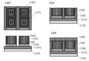
일 실시예로, 도 1 및 2에 도시된 바와 같이, 본 발명의 복수의 카본 나노 튜브층(140)은 제1 카본 나노 튜브층(141), 제2 카본 나노 튜브층(142) 및 제3 카본 나노 튜브층(143)을 포함할 수 있다.In one embodiment, as shown in FIGS. 1 and 2 , the plurality of
제1 카본 나노 튜브층(141)은 20 내지 80 nm 의 길이를 갖는 카본 나노 튜브들을 포함할 수 있다.The first
제2 카본 나노 튜브층(142)은 제1 카본 나노 튜브층(141)의 상부 영역 일부에 형성되고, 100 내지 200 nm 의 길이를 갖는 카본 나노 튜브들을 포함할 수 있다.The second
제3 카본 나노 튜브층(143)은 제2 카본 나노 튜브층(142)의 상부 영역 일부에 형성되고, 300 내지 500 nm 의 길이를 갖는 카본 나노 튜브들을 포함할 수 있다.The third
상술한 바와 같이, 도 1에 도시된 카본 나노 튜브층(140)은 각 층에 서로 다른 길이의 카본 나노 튜브들을 포함하기에, 외부 전기장의 인가 시에 카본 나노 튜브들의 배열이 점진적으로 변화하여 시냅스 소자의 저항과 전기 전도도를 선형적으로 변화시킬 수 있다. 또한, 본 발명은 이에 제한되는 것이 아니라, 시냅스 소자(100)의 목표 성능에 따라 각 층에 포함된 카본 나노 튜브들의 길이, 두께, 벽수, 극성 작용기 유무를 유연하게 변경할 수 있다.As described above, since the
한편, 본 발명의 복수의 카본 나노 튜브층(140)은 법선이 중력 방향에 수직으로 배치된 구조를 가질 수 있다. 즉, 복수의 카본 나노 튜브층(140)이 상부 전극(130)과 하부 전극(120) 사이에서 병렬 구조로 배치됨에 따라, 저항이 감소되며 정렬하여 누워있는 카본 나노 튜브들의 효율적인 움직임을 가능하게 하여 점진적으로 전기 전도도를 변화시킬 수 있다.On the other hand, the plurality of carbon nanotube layers 140 of the present invention may have a structure in which normals are arranged perpendicular to the direction of gravity. That is, as the plurality of carbon nanotube layers 140 are arranged in a parallel structure between the
도 3a-c 는 본 발명의 일 실시예인 인공 시냅스 소자의 동작 원리를 설명하기 위한 도면이다.Figure 3a-c is a view for explaining the operation principle of the artificial synaptic device according to an embodiment of the present invention.
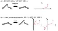
도 3a 에 나타나듯이, 외부 전기장에 의해 카본 나노 튜브들 간의 정전기적 인력이 발생하며, 이러한 인력이 카본 나노 튜브들의 거동을 유발하여 카본 나노 튜브간의 접촉(SET)이 발생하여 저항이 감소하면서 많은 전류 통로가 생성된다.As shown in FIG. 3A , an electrostatic attraction between the carbon nanotubes is generated by an external electric field, and this attraction causes the carbon nanotubes to behave, so that a contact (SET) between the carbon nanotubes occurs, resulting in a decrease in resistance and a large amount of current passage is created.
반면, 반대 극성의 펄스를 인가하여 댐핑을 유도하여 댐핑이 일정 수준을 넘을 경우, 포논 여기(phonon excitation) 와 함께 접촉이 떨어지는 비접촉(RESET)이 유도되고, 이에 따라 저항이 증가하게 된다.On the other hand, when damping is induced by applying a pulse of opposite polarity and the damping exceeds a certain level, a non-contact (RESET) in which the contact is dropped along with phonon excitation is induced, thereby increasing the resistance.
이때, 도 3b 에 도시된 바와 같이, 카본 나노 튜브들의 거동은 카본 나노 튜브들의 길이, 두께, 벽수, 극성 작용기 유무 등에 영향을 받는다. 구체적으로, 카본 나노 튜브들의 길이가 짧고, 두께가 얇으며, 표면에 극성 작용기가 도입된 경우, 이러한 거동은 더욱 즉각적이다.At this time, as shown in FIG. 3B , the behavior of the carbon nanotubes is affected by the length, thickness, number of walls, the presence or absence of a polar functional group, and the like of the carbon nanotubes. Specifically, when the carbon nanotubes have a short length, a thin thickness, and a polar functional group is introduced on the surface, this behavior is more immediate.
따라서, 본 발명은 외부 전기장에 대해 서로 다른 거동 특성을 갖는 카본 나노 튜브들을 각 층(140)에 배치하여, 외부 전기장의 인가 시에 카본 나노 튜브들의 배열이 점진적으로 변화하도록 함으로써, 시냅스 소자의 저항과 전기 전도도를 선형적으로 변화시킬 수 있다.Accordingly, the present invention arranges carbon nanotubes having different behavioral characteristics with respect to an external electric field on each
아울러, 이러한 카본 나노 튜브층(140)이 상부 전극(130)과 하부 전극(120) 사이에서 병렬 구조로 배치되어 있기에, 저항을 줄여 인공 시냅스 소자(100)의 에너지 효율을 극대화할 수 있다.In addition, since the
한편, 다시 도 1을 참조하면, 상기 복수의 카본 나노 튜브층(140) 사이에는 절연 물질로 이루어진 격벽(150)이 형성될 수 있다.Meanwhile, referring back to FIG. 1 , a
상기 격벽(150)은 카본 나노 튜브층(140)에 각각 존재하는 카본 나노 튜브들이 혼합되는 것을 방지하기 위한 것이며, 격벽(150)의 존재로 인해 각 층의 카본 나노 튜브들이 서로 혼합되지 않아, 인공 시냅스 소자(100)가 장기간 동안에도 안정성을 유지할 수 있고, 이로 인해 시냅스 소자(100)의 수명이 연장될 수 있다.The
이때, 상기 격벽(150)을 이루는 절연 물질은 이산화규소(SiO2), 산화알루미늄(Al2O3), 산화하프늄(HfO2), 질화규소(Si3N4), 실리콘 산질화물(SiON), 산화마그네슘(MgO), 산화칼슘(CaO), 지르코늄실리케이트(ZrSiO4), 산화지르코늄(ZrO2), 산화란탄륨(La2O3), 오산화탄탈럼(Ta2O5), 스트론튬 산화물(SrO) 및 바륨 산화물(BaO) 중에서 선택된 어느 하나 이상을 포함하는 것이 바람직하나, 이에 제한되는 것은 아니다.At this time, the insulating material constituting the
한편, 본 발명의 인공 시냅스 소자(100)는 복수의 카본 나노 튜브층(140)의 법선이 중력 방향에 수직으로 배치된 구조를 가지기에, 도 2에 도시된 바와 같이, 크로스 포인트(cross-point) 시냅스 어레이 구조를 구현할 경우 월등한 집적도를 구현할 수 있으며, 나아가 M3D 집적 등의 추가적인 수직형 구조를 구현할 수 있다.On the other hand, since the artificial
도 4a-c는 본 발명의 일 실시예에 따른 인공 시냅스 소자 제조 방법을 설명하기 위한 것이다.Figure 4a-c is for explaining an artificial synaptic device manufacturing method according to an embodiment of the present invention.
도 4a-c를 참조하면, 본 발명의 일 실시예에 따른 인공 시냅스 소자 제조 방법은 상부면에 절연층이 형성된 기판 상에 하부 전극을 형성하는 단계(S100), 상기 하부 전극 상에 서로 다른 길이 또는 두께의 카본 나노 튜브들을 각각 포함하는 복수의 카본 나노 튜브층을 법선이 중력 방향에 수직으로 배치되도록 형성하는 단계(S200), 상기 복수의 카본 나노 튜브층 간에 간극이 형성되도록 식각하는 단계(S300), 상기 간극을 절연 물질로 패시베이션하는 단계(S400), 및 상기 복수의 카본 나노 튜브층 상에 상부 전극을 형성하는 단계(S500)를 포함한다.Referring to Figures 4a-c, the artificial synaptic device manufacturing method according to an embodiment of the present invention is the step of forming a lower electrode on a substrate having an insulating layer formed on the upper surface (S100), different lengths on the lower electrode Alternatively, forming a plurality of carbon nanotube layers each having a thickness of carbon nanotubes so that a normal line is disposed perpendicular to the direction of gravity (S200), and etching to form gaps between the plurality of carbon nanotube layers (S300) ), passivating the gap with an insulating material (S400), and forming an upper electrode on the plurality of carbon nanotube layers (S500).
먼저, 상부면에 절연층이 형성된 기판 상에 하부 전극을 형성하는 단계(S100)를 진행한다.First, a step (S100) of forming a lower electrode on a substrate on which an insulating layer is formed on the upper surface is performed.
일 실시예로, 도 4a를 참조하면, 기판(110)의 상부면에 절연층(111)을 형성한 후, 하부 전극(120)을 형성할 수 있다. 이때, 절연층(111)은 증착 공정 또는 산화 공정을 통해 기판(110) 상에 형성될 수 있고, 하부 전극(120)은 증착 공정, 식각 공정 등을 이용하여 전도성 물질인 금, 백금 등을 형성할 수 있으나, 이에 제한되는 것은 아니다.For example, referring to FIG. 4A , after the insulating
다음으로, 상기 하부 전극 상에 서로 다른 길이 또는 두께의 카본 나노 튜브들을 각각 포함하는 복수의 카본 나노 튜브층을 법선이 중력 방향에 수직으로 배치되도록 형성하는 단계(S200)를 진행한다(도 4b 참조).Next, a step (S200) of forming a plurality of carbon nanotube layers each including carbon nanotubes of different lengths or thicknesses on the lower electrode so that a normal line is disposed perpendicular to the direction of gravity (see FIG. 4b ) is performed. ).
여기서, 각 층에 포함되는 카본 나노 튜브들 중 일부의 표면에는 극성 작용기가 도입될 수 있다. 즉, 각 층은 극성 작용기가 도입된 카본 나노 튜브들와 극성 작용기가 도입되지 않은 카본 나노 튜브들이 혼합되어 구성될 수 있다. 또한, 상기 복수의 카본 나노 튜브층은 서로 다른 길이, 두께의 카본 나노 튜브들을 각각 포함할 수 있다. 그리고, 상기 카본 나노 튜브들은 단일벽, 이중 벽 또는 삼중벽을 가질 수 있다.Here, a polar functional group may be introduced into the surface of some of the carbon nanotubes included in each layer. That is, each layer may be composed of a mixture of carbon nanotubes to which polar functional groups are introduced and carbon nanotubes to which polar functional groups are not introduced. Also, the plurality of carbon nanotube layers may include carbon nanotubes of different lengths and thicknesses, respectively. In addition, the carbon nanotubes may have a single wall, a double wall, or a triple wall.
일 실시예로, 상기 복수의 카본 나노 튜브층(140)은 다음과 같은 단계를 통해 형성될 수 있다.In an embodiment, the plurality of carbon nanotube layers 140 may be formed through the following steps.
먼저, 20 내지 80 nm 의 길이를 갖는 카본 나노 튜브들을 포함하는 제1 카본 나노 튜브층을 형성하는 단계(S210)를 수행할 수 있다. 이때, 상기 제1 카본 나노 튜브층(141)은 스핀 코팅 공정을 이용하여 형성하는 것이 바람직하나, 이에 제한되는 것은 아니다.First, the step of forming a first carbon nanotube layer including carbon nanotubes having a length of 20 to 80 nm (S210) may be performed. In this case, the first
다음으로, 제1 카본 나노 튜브층(141)의 상부 영역 일부에 100 내지 200 nm 의 길이를 갖는 카본 나노 튜브들을 포함하는 제2 카본 나노 튜브층(142)을 형성하는 단계(S220)를 수행한다.Next, a step (S220) of forming a second
이후, 상기 제2 카본 나노 튜브층(142)의 상부 영역 일부에 300 내지 400 nm 의 길이를 갖는 카본 나노 튜브들을 포함하는 제3 카본 나노 튜브층(143)을 형성하는 단계(S230)을 수행한다.Thereafter, a step (S230) of forming a third
이때, 상기 제2 및 제3 카본 나노 튜브층(142, 143) 또한 스핀 코팅 공정을 이용하여 형성할 수 있으며, 상기 단계들을 통해 제조된 복수의 카본 나노 튜브층(141, 142, 143)은 법선이 중력 방향에 수직으로 배치되도록 형성된다.At this time, the second and third carbon nanotube layers 142 and 143 may also be formed by using a spin coating process, and the plurality of carbon nanotube layers 141 , 142 , 143 manufactured through the above steps may have a normal line. It is formed so as to be disposed perpendicular to the direction of gravity.
다음으로, 도 4c를 참조하면, 상기 복수의 카본 나노 튜브층 간에 간극이 형성되도록 식각하는 단계(S300)를 수행한다.Next, referring to FIG. 4C , an etching step ( S300 ) is performed to form gaps between the plurality of carbon nanotube layers.
일 실시예로, 카본 나노 튜브층(140) 간에 접촉되는 영역에 패턴을 형성한 후, 식각 공정을 통해 식각함으로써 간극(150a)을 형성할 수 있다.In an embodiment, the gap 150a may be formed by forming a pattern in a region in contact between the carbon nanotube layers 140 and then etching through an etching process.
이후, 상기 간극(150a)을 절연 물질로 패시베이션하는 단계(S400)를 수행하며, 이를 통해 카본 나노 튜브층(140) 사이에는 절연 물질로 이루어진 격벽(150)이 형성되게 된다. 이때, 상기 절연 물질은 이산화규소(SiO2), 산화알루미늄(Al2O3), 산화하프늄(HfO2), 질화규소(Si3N4), 실리콘 산질화물(SiON), 산화마그네슘(MgO), 산화칼슘(CaO), 지르코늄실리케이트(ZrSiO4), 산화지르코늄(ZrO2), 산화란탄륨(La2O3), 오산화탄탈럼(Ta2O5), 스트론튬 산화물(SrO), 바륨 산화물(BaO) 등을 사용할 수 있으나, 이에 제한되는 것은 아니다.Thereafter, a step ( S400 ) of passivating the gap 150a with an insulating material is performed, whereby the
일 실시예로, 상기 격벽(150)의 형성은 증착 공정 등을 통해 수행할 수 있고, 패시베이션하는 단계(S400) 후에, CMP 공정을 수행하여 복수의 카본 나노 튜브층(140)의 표면을 평탄화할 수 있다.In one embodiment, the
다음으로, 상기 복수의 카본 나노 튜브층 상에 상부 전극을 형성하는 단계(S500)를 수행하여, 본 발명에 따른 인공 시냅스 소자를 제조할 수 있다.Next, by performing the step (S500) of forming an upper electrode on the plurality of carbon nanotube layers, an artificial synaptic device according to the present invention can be manufactured.
이때, 상부 전극(130)은 증착 공정, 식각 공정 등을 이용하여 전도성 물질인 금, 백금 등을 형성할 수 있으나, 이에 제한되는 것은 아니다.In this case, the
본 발명에 따르면, 상기 복수의 카본 나노 튜브층(140) 사이의 간극(150a)을 절연 물질로 패시베이션하여 격벽(150)을 형성함에 따라, 카본 나노 튜브층(140)에 각각 존재하는 카본 나노 튜브들의 혼합이 방지되어, 장기간 동안에도 소자의 안정성을 유지할 수 있고, 이로 인해 시냅스 소자의 수명을 연장할 수 있다.According to the present invention, as the
상기에서는 본 발명의 바람직한 실시예를 참조하여 설명하였지만, 해당 기술분야의 숙련된 당업자는 하기의 특허 청구 범위에 기재된 본 발명의 사상 및 영역으로부터 벗어나지 않는 범위 내에서 본 발명을 다양하게 수정 및 변경시킬 수 있음을 이해할 수 있을 것이다.Although the above has been described with reference to the preferred embodiments of the present invention, those skilled in the art can variously modify and change the present invention without departing from the spirit and scope of the present invention as set forth in the following claims. You will understand that you can.
100 : 인공 시냅스 소자110 : 기판
111 : 절연층120 : 상부 전극
130 : 하부 전극140 : 카본 나노 튜브층
141 : 제1 카본 나노 튜브층142 : 제2 카본 나노 튜브층
143 : 제3 카본 나노 튜브층150a : 간극
150 : 격벽100: artificial synaptic element 110: substrate
111: insulating layer 120: upper electrode
130: lower electrode 140: carbon nanotube layer
141: first carbon nanotube layer 142: second carbon nanotube layer
143: third carbon nanotube layer 150a: gap
150: bulkhead
Claims (13)
Translated fromKorean상부 전극; 및
상기 하부 전극과 상부 전극 사이에 배치되고, 서로 다른 길이 또는 두께의 카본 나노 튜브들을 각각 포함하는 복수의 카본 나노 튜브층;을 포함하고,
상기 복수의 카본 나노 튜브층은 법선이 중력 방향에 수직으로 배치된 구조를 갖는 것인,
인공 시냅스 소자.
a lower electrode disposed on the substrate;
upper electrode; and
a plurality of carbon nanotube layers disposed between the lower electrode and the upper electrode and each including carbon nanotubes of different lengths or thicknesses;
The plurality of carbon nanotube layers have a structure in which normals are arranged perpendicular to the direction of gravity.
artificial synaptic device.
상기 복수의 카본 나노 튜브층은,
20 내지 80 nm 의 길이를 갖는 카본 나노 튜브들을 포함하는 제1 카본 나노 튜브층;
상기 제1 카본 나노 튜브층의 상부 영역 일부에 형성되고, 100 내지 200 nm 의 길이를 갖는 카본 나노 튜브들을 포함하는 제2 카본 나노 튜브층; 및
상기 제2 카본 나노 튜브층의 상부 영역 일부에 형성되고, 300 내지 500 nm 의 길이를 갖는 카본 나노 튜브들을 포함하는 제3 카본 나노 튜브층;을 포함하는 것을 특징으로 하는,
인공 시냅스 소자.
According to claim 1,
The plurality of carbon nanotube layers,
a first carbon nanotube layer including carbon nanotubes having a length of 20 to 80 nm;
a second carbon nanotube layer formed on a portion of an upper region of the first carbon nanotube layer and including carbon nanotubes having a length of 100 to 200 nm; and
and a third carbon nanotube layer formed on a portion of an upper region of the second carbon nanotube layer and including carbon nanotubes having a length of 300 to 500 nm;
artificial synaptic device.
상기 복수의 카본 나노 튜브층 사이에는 절연 물질로 이루어진 격벽이 형성된 것을 특징으로 하는,
인공 시냅스 소자.
According to claim 1,
A barrier rib made of an insulating material is formed between the plurality of carbon nanotube layers,
artificial synaptic device.
상기 절연 물질은 이산화규소(SiO2), 산화알루미늄(Al2O3), 산화하프늄(HfO2), 질화규소(Si3N4), 실리콘 산질화물(SiON), 산화마그네슘(MgO), 산화칼슘(CaO), 지르코늄실리케이트(ZrSiO4), 산화지르코늄(ZrO2), 산화란탄륨(La2O3), 오산화탄탈럼(Ta2O5), 스트론튬 산화물(SrO) 및 바륨 산화물(BaO) 중에서 선택된 어느 하나 이상을 포함하는 것을 특징으로 하는,
인공 시냅스 소자.
4. The method of claim 3,
The insulating material is silicon dioxide (SiO2 ), aluminum oxide (Al2 O3 ), hafnium oxide (HfO2 ), silicon nitride (Si3 N4 ), silicon oxynitride (SiON), magnesium oxide (MgO), calcium oxide (CaO), zirconium silicate (ZrSiO4 ), zirconium oxide (ZrO2 ), lanthanum oxide (La2 O3 ), tantalum pentoxide (Ta2 O5 ), strontium oxide (SrO) and barium oxide (BaO) Characterized in comprising one or more selected one,
artificial synaptic device.
상기 카본 나노 튜브들 중 일부의 표면에는 극성 작용기가 도입된 것을 특징으로 하는,
인공 시냅스 소자.
According to claim 1,
A polar functional group is introduced on the surface of some of the carbon nanotubes,
artificial synaptic device.
상기 극성 작용기는 카르복시기(-COOH), 아미드기(-CONH2), 옥타데실아민기 및 플루오로 페닐기 중에서 선택된 어느 하나 이상을 포함하는 것을 특징으로 하는,
인공 시냅스 소자.
6. The method of claim 5,
The polar functional group is characterized in that it comprises at least one selected from a carboxyl group (-COOH), an amide group (-CONH2 ), an octadecylamine group, and a fluorophenyl group,
artificial synaptic device.
상기 기판은 실리콘(Si), 저마늄(Ge), 유리 및 PET 필름 중에서 선택된 물질로 이루어지고,
상기 기판 상에는 이산화규소(SiO2), 산화알루미늄(Al2O3), 산화하프늄(HfO2), 질화규소(Si3N4), 실리콘 산질화물(SiON), 산화마그네슘(MgO), 산화칼슘(CaO), 지르코늄실리케이트(ZrSiO4), 산화지르코늄(ZrO2), 산화란탄륨(La2O3), 오산화탄탈럼(Ta2O5), 스트론튬 산화물(SrO) 및 바륨 산화물(BaO) 중에서 선택된 절연 물질을 포함하는 절연층이 형성된 것을 특징으로 하는,
인공 시냅스 소자.
According to claim 1,
The substrate is made of a material selected from silicon (Si), germanium (Ge), glass and PET film,
On the substrate, silicon dioxide (SiO2 ), aluminum oxide (Al2 O3 ), hafnium oxide (HfO2 ), silicon nitride (Si3 N4 ), silicon oxynitride (SiON), magnesium oxide (MgO), calcium oxide ( CaO), zirconium silicate (ZrSiO4 ), zirconium oxide (ZrO2 ), lanthanum oxide (La2 O3 ), tantalum pentoxide (Ta2 O5 ), strontium oxide (SrO) and barium oxide (BaO) Characterized in that an insulating layer comprising an insulating material is formed,
artificial synaptic device.
상기 하부 전극 및 상부 전극은 금(Au), 백금(Pt), 티타늄(Ti), 크롬(Cr), 팔라듐(Pd) 및 로듐(Rh) 중에서 선택된 어느 하나 이상을 포함하는 것을 특징으로 하는,
인공 시냅스 소자.
According to claim 1,
The lower electrode and the upper electrode are characterized in that they contain any one or more selected from gold (Au), platinum (Pt), titanium (Ti), chromium (Cr), palladium (Pd), and rhodium (Rh),
artificial synaptic device.
상기 하부 전극 상에 서로 다른 길이 또는 두께의 카본 나노 튜브들을 각각 포함하는 복수의 카본 나노 튜브층을 법선이 중력 방향에 수직으로 배치되도록 형성하는 단계;
상기 복수의 카본 나노 튜브층 간에 간극이 형성되도록 식각하는 단계;
상기 간극을 절연 물질로 패시베이션하는 단계; 및
상기 복수의 카본 나노 튜브층 상에 상부 전극을 형성하는 단계;를 포함하는,
인공 시냅스 소자 제조 방법.
forming a lower electrode on a substrate having an insulating layer formed on its upper surface;
forming a plurality of carbon nanotube layers each including carbon nanotubes of different lengths or thicknesses on the lower electrode so that a normal line is disposed perpendicular to a direction of gravity;
etching to form gaps between the plurality of carbon nanotube layers;
passivating the gap with an insulating material; and
Including; forming an upper electrode on the plurality of carbon nanotube layers;
A method for manufacturing an artificial synaptic device.
상기 복수의 카본 나노 튜브층을 형성하는 단계는,
20 내지 80 nm 의 길이를 갖는 카본 나노 튜브들을 포함하는 제1 카본 나노 튜브층을 형성하는 단계;
상기 제1 카본 나노 튜브층의 상부 영역 일부에 100 내지 200 nm 의 길이를 갖는 카본 나노 튜브들을 포함하는 제2 카본 나노 튜브층을 형성하는 단계; 및
상기 제2 카본 나노 튜브층의 상부 영역 일부에 300 내지 500 nm 의 길이를 갖는 카본 나노 튜브들을 포함하는 제3 카본 나노 튜브층을 형성하는 단계;를 포함하는 것을 특징으로 하는,
인공 시냅스 소자 제조 방법.
10. The method of claim 9,
Forming the plurality of carbon nanotube layers comprises:
forming a first carbon nanotube layer including carbon nanotubes having a length of 20 to 80 nm;
forming a second carbon nanotube layer including carbon nanotubes having a length of 100 to 200 nm in a portion of an upper region of the first carbon nanotube layer; and
forming a third carbon nanotube layer including carbon nanotubes having a length of 300 to 500 nm on a part of an upper region of the second carbon nanotube layer;
A method for manufacturing an artificial synaptic device.
상기 카본 나노 튜브들 중 일부의 표면에는 극성 작용기가 도입된 것을 특징으로 하는,
인공 시냅스 소자 제조 방법.
10. The method of claim 9,
A polar functional group is introduced on the surface of some of the carbon nanotubes,
A method for manufacturing an artificial synaptic device.
상기 극성 작용기는 카르복시기(-COOH), 아미드기(-CONH2), 옥타데실아민기 및 플루오로 페닐기 중에서 선택된 어느 하나 이상을 포함하는 것을 특징으로 하는,
인공 시냅스 소자 제조 방법.
12. The method of claim 11,
The polar functional group is characterized in that it comprises at least one selected from a carboxyl group (-COOH), an amide group (-CONH2 ), an octadecylamine group, and a fluorophenyl group,
A method for manufacturing an artificial synaptic device.
상기 절연 물질은 이산화규소(SiO2), 산화알루미늄(Al2O3), 산화하프늄(HfO2), 질화규소(Si3N4), 실리콘 산질화물(SiON), 산화마그네슘(MgO), 산화칼슘(CaO), 지르코늄실리케이트(ZrSiO4), 산화지르코늄(ZrO2), 산화란탄륨(La2O3), 오산화탄탈럼(Ta2O5), 스트론튬 산화물(SrO) 및 바륨 산화물(BaO) 중에서 선택된 어느 하나 이상을 포함하는 것을 특징으로 하는,
인공 시냅스 소자 제조 방법.10. The method of claim 9,
The insulating material is silicon dioxide (SiO2 ), aluminum oxide (Al2 O3 ), hafnium oxide (HfO2 ), silicon nitride (Si3 N4 ), silicon oxynitride (SiON), magnesium oxide (MgO), calcium oxide (CaO), zirconium silicate (ZrSiO4 ), zirconium oxide (ZrO2 ), lanthanum oxide (La2 O3 ), tantalum pentoxide (Ta2 O5 ), strontium oxide (SrO) and barium oxide (BaO) Characterized in comprising one or more selected one,
A method for manufacturing an artificial synaptic device.
Priority Applications (1)
| Application Number | Priority Date | Filing Date | Title |
|---|---|---|---|
| KR1020200119915AKR102301330B1 (en) | 2020-09-17 | 2020-09-17 | Artificial synaptic device and method for manufacturing the same |
Applications Claiming Priority (1)
| Application Number | Priority Date | Filing Date | Title |
|---|---|---|---|
| KR1020200119915AKR102301330B1 (en) | 2020-09-17 | 2020-09-17 | Artificial synaptic device and method for manufacturing the same |
Publications (1)
| Publication Number | Publication Date |
|---|---|
| KR102301330B1true KR102301330B1 (en) | 2021-09-13 |
Family
ID=77796560
Family Applications (1)
| Application Number | Title | Priority Date | Filing Date |
|---|---|---|---|
| KR1020200119915AActiveKR102301330B1 (en) | 2020-09-17 | 2020-09-17 | Artificial synaptic device and method for manufacturing the same |
Country Status (1)
| Country | Link |
|---|---|
| KR (1) | KR102301330B1 (en) |
Citations (2)
| Publication number | Priority date | Publication date | Assignee | Title |
|---|---|---|---|---|
| KR20150014577A (en)* | 2013-07-29 | 2015-02-09 | 삼성전자주식회사 | Nonvolatile memory transistor and device including the same |
| KR20160019682A (en)* | 2014-08-12 | 2016-02-22 | 포항공과대학교 산학협력단 | Device imitating synaptic and method of manufacturing thereof |
- 2020
- 2020-09-17KRKR1020200119915Apatent/KR102301330B1/enactiveActive
Patent Citations (2)
| Publication number | Priority date | Publication date | Assignee | Title |
|---|---|---|---|---|
| KR20150014577A (en)* | 2013-07-29 | 2015-02-09 | 삼성전자주식회사 | Nonvolatile memory transistor and device including the same |
| KR20160019682A (en)* | 2014-08-12 | 2016-02-22 | 포항공과대학교 산학협력단 | Device imitating synaptic and method of manufacturing thereof |
Similar Documents
| Publication | Publication Date | Title |
|---|---|---|
| JP7584899B2 (en) | Memristor and neuromorphic device including same | |
| US8847188B2 (en) | Switching device and memory device including the same | |
| Kügeler et al. | High density 3D memory architecture based on the resistive switching effect | |
| US6940740B2 (en) | Multilevel semiconductor memory device and method for driving the same as a neuron element in a neural network computer | |
| JP2019179499A (en) | Semiconductor device and product-sum computation device | |
| CN103579500B (en) | Resistance switch material elements and the device using the resistance switch material elements | |
| US8362457B2 (en) | Semiconductor device and method for fabricating the same | |
| US20080012047A1 (en) | Two-terminal nanotube devices and systems and methods of making same | |
| CN107591479B (en) | Resistive random access memory | |
| CN101292300B (en) | Nanoscale shift register and signal demultiplexing using microscale/nanoscale shift registers | |
| CN101064359A (en) | Non-volatile memory devices including variable resistance material | |
| CN101536188A (en) | Resistive memory element, method for manufacturing the same, and nonvolatile semiconductor memory device | |
| CN107068859B (en) | Nanoparticle matrix for three-dimensional non-volatile resistive random access memory | |
| US20110204310A1 (en) | Electronic device incorporating memristor made from metallic nanowire | |
| KR102301330B1 (en) | Artificial synaptic device and method for manufacturing the same | |
| Lu et al. | Highly Uniform Two‐Terminal Artificial Synapses Based on Polycrystalline Hf0. 5Zr0. 5O2 for Sparsified Back Propagation Networks | |
| Tager et al. | Spontaneous charge polarization in single-electron tunneling through coupled nanowires | |
| KR101460122B1 (en) | Negative differential resistance device | |
| US20170141306A1 (en) | Memory structure | |
| TWI683366B (en) | Variable resistance element and memory device | |
| WO2013137913A1 (en) | Varied multilayer memristive device | |
| US9087609B2 (en) | Multi-bit memory device | |
| KR102358221B1 (en) | Multilayered memristor device including amorphous silicon and dielectric for providing analog synapse behavior | |
| CN112086556B (en) | Memory cells and methods of forming the same | |
| Pi et al. | Device engineering and CMOS integration of nanoscale memristors |
Legal Events
| Date | Code | Title | Description |
|---|---|---|---|
| PA0109 | Patent application | Patent event code:PA01091R01D Comment text:Patent Application Patent event date:20200917 | |
| PA0201 | Request for examination | ||
| E701 | Decision to grant or registration of patent right | ||
| PE0701 | Decision of registration | Patent event code:PE07011S01D Comment text:Decision to Grant Registration Patent event date:20210906 | |
| GRNT | Written decision to grant | ||
| PR0701 | Registration of establishment | Comment text:Registration of Establishment Patent event date:20210907 Patent event code:PR07011E01D | |
| PR1002 | Payment of registration fee | Payment date:20210907 End annual number:3 Start annual number:1 | |
| PG1601 | Publication of registration | ||
| PR1001 | Payment of annual fee | Payment date:20240625 Start annual number:4 End annual number:4 |