KR102293599B1 - Electronic appliance - Google Patents
Electronic applianceDownload PDFInfo
- Publication number
- KR102293599B1 KR102293599B1KR1020140187458AKR20140187458AKR102293599B1KR 102293599 B1KR102293599 B1KR 102293599B1KR 1020140187458 AKR1020140187458 AKR 1020140187458AKR 20140187458 AKR20140187458 AKR 20140187458AKR 102293599 B1KR102293599 B1KR 102293599B1
- Authority
- KR
- South Korea
- Prior art keywords
- light
- guide layer
- light guide
- image
- light source
- Prior art date
- Legal status (The legal status is an assumption and is not a legal conclusion. Google has not performed a legal analysis and makes no representation as to the accuracy of the status listed.)
- Active
Links
Images


Classifications
- G—PHYSICS
- G02—OPTICS
- G02F—OPTICAL DEVICES OR ARRANGEMENTS FOR THE CONTROL OF LIGHT BY MODIFICATION OF THE OPTICAL PROPERTIES OF THE MEDIA OF THE ELEMENTS INVOLVED THEREIN; NON-LINEAR OPTICS; FREQUENCY-CHANGING OF LIGHT; OPTICAL LOGIC ELEMENTS; OPTICAL ANALOGUE/DIGITAL CONVERTERS
- G02F1/00—Devices or arrangements for the control of the intensity, colour, phase, polarisation or direction of light arriving from an independent light source, e.g. switching, gating or modulating; Non-linear optics
- G02F1/01—Devices or arrangements for the control of the intensity, colour, phase, polarisation or direction of light arriving from an independent light source, e.g. switching, gating or modulating; Non-linear optics for the control of the intensity, phase, polarisation or colour
- G02F1/13—Devices or arrangements for the control of the intensity, colour, phase, polarisation or direction of light arriving from an independent light source, e.g. switching, gating or modulating; Non-linear optics for the control of the intensity, phase, polarisation or colour based on liquid crystals, e.g. single liquid crystal display cells
- G02F1/133—Constructional arrangements; Operation of liquid crystal cells; Circuit arrangements
- G02F1/1333—Constructional arrangements; Manufacturing methods
- G02F1/1335—Structural association of cells with optical devices, e.g. polarisers or reflectors
- G02F1/133524—Light-guides, e.g. fibre-optic bundles, louvered or jalousie light-guides
- G—PHYSICS
- G09—EDUCATION; CRYPTOGRAPHY; DISPLAY; ADVERTISING; SEALS
- G09F—DISPLAYING; ADVERTISING; SIGNS; LABELS OR NAME-PLATES; SEALS
- G09F9/00—Indicating arrangements for variable information in which the information is built-up on a support by selection or combination of individual elements
- G09F9/30—Indicating arrangements for variable information in which the information is built-up on a support by selection or combination of individual elements in which the desired character or characters are formed by combining individual elements
- G09F9/33—Indicating arrangements for variable information in which the information is built-up on a support by selection or combination of individual elements in which the desired character or characters are formed by combining individual elements being semiconductor devices, e.g. diodes
- G—PHYSICS
- G02—OPTICS
- G02B—OPTICAL ELEMENTS, SYSTEMS OR APPARATUS
- G02B6/00—Light guides; Structural details of arrangements comprising light guides and other optical elements, e.g. couplings
- G02B6/0001—Light guides; Structural details of arrangements comprising light guides and other optical elements, e.g. couplings specially adapted for lighting devices or systems
- G02B6/0011—Light guides; Structural details of arrangements comprising light guides and other optical elements, e.g. couplings specially adapted for lighting devices or systems the light guides being planar or of plate-like form
- G02B6/0075—Arrangements of multiple light guides
- G02B6/0076—Stacked arrangements of multiple light guides of the same or different cross-sectional area
- F—MECHANICAL ENGINEERING; LIGHTING; HEATING; WEAPONS; BLASTING
- F21—LIGHTING
- F21V—FUNCTIONAL FEATURES OR DETAILS OF LIGHTING DEVICES OR SYSTEMS THEREOF; STRUCTURAL COMBINATIONS OF LIGHTING DEVICES WITH OTHER ARTICLES, NOT OTHERWISE PROVIDED FOR
- F21V23/00—Arrangement of electric circuit elements in or on lighting devices
- F21V23/04—Arrangement of electric circuit elements in or on lighting devices the elements being switches
- F—MECHANICAL ENGINEERING; LIGHTING; HEATING; WEAPONS; BLASTING
- F21—LIGHTING
- F21V—FUNCTIONAL FEATURES OR DETAILS OF LIGHTING DEVICES OR SYSTEMS THEREOF; STRUCTURAL COMBINATIONS OF LIGHTING DEVICES WITH OTHER ARTICLES, NOT OTHERWISE PROVIDED FOR
- F21V33/00—Structural combinations of lighting devices with other articles, not otherwise provided for
- F21V33/0004—Personal or domestic articles
- F21V33/0044—Household appliances, e.g. washing machines or vacuum cleaners
- G—PHYSICS
- G02—OPTICS
- G02B—OPTICAL ELEMENTS, SYSTEMS OR APPARATUS
- G02B6/00—Light guides; Structural details of arrangements comprising light guides and other optical elements, e.g. couplings
- G02B6/0001—Light guides; Structural details of arrangements comprising light guides and other optical elements, e.g. couplings specially adapted for lighting devices or systems
- G02B6/0011—Light guides; Structural details of arrangements comprising light guides and other optical elements, e.g. couplings specially adapted for lighting devices or systems the light guides being planar or of plate-like form
- G02B6/0013—Means for improving the coupling-in of light from the light source into the light guide
- G02B6/0023—Means for improving the coupling-in of light from the light source into the light guide provided by one optical element, or plurality thereof, placed between the light guide and the light source, or around the light source
- G—PHYSICS
- G02—OPTICS
- G02B—OPTICAL ELEMENTS, SYSTEMS OR APPARATUS
- G02B6/00—Light guides; Structural details of arrangements comprising light guides and other optical elements, e.g. couplings
- G02B6/0001—Light guides; Structural details of arrangements comprising light guides and other optical elements, e.g. couplings specially adapted for lighting devices or systems
- G02B6/0011—Light guides; Structural details of arrangements comprising light guides and other optical elements, e.g. couplings specially adapted for lighting devices or systems the light guides being planar or of plate-like form
- G02B6/0033—Means for improving the coupling-out of light from the light guide
- G02B6/005—Means for improving the coupling-out of light from the light guide provided by one optical element, or plurality thereof, placed on the light output side of the light guide
- G02B6/0055—Reflecting element, sheet or layer
- G—PHYSICS
- G02—OPTICS
- G02B—OPTICAL ELEMENTS, SYSTEMS OR APPARATUS
- G02B6/00—Light guides; Structural details of arrangements comprising light guides and other optical elements, e.g. couplings
- G02B6/0001—Light guides; Structural details of arrangements comprising light guides and other optical elements, e.g. couplings specially adapted for lighting devices or systems
- G02B6/0011—Light guides; Structural details of arrangements comprising light guides and other optical elements, e.g. couplings specially adapted for lighting devices or systems the light guides being planar or of plate-like form
- G02B6/0065—Manufacturing aspects; Material aspects
- G—PHYSICS
- G02—OPTICS
- G02B—OPTICAL ELEMENTS, SYSTEMS OR APPARATUS
- G02B6/00—Light guides; Structural details of arrangements comprising light guides and other optical elements, e.g. couplings
- G02B6/0001—Light guides; Structural details of arrangements comprising light guides and other optical elements, e.g. couplings specially adapted for lighting devices or systems
- G02B6/0011—Light guides; Structural details of arrangements comprising light guides and other optical elements, e.g. couplings specially adapted for lighting devices or systems the light guides being planar or of plate-like form
- G02B6/0066—Light guides; Structural details of arrangements comprising light guides and other optical elements, e.g. couplings specially adapted for lighting devices or systems the light guides being planar or of plate-like form characterised by the light source being coupled to the light guide
- G02B6/0068—Arrangements of plural sources, e.g. multi-colour light sources
- G—PHYSICS
- G02—OPTICS
- G02B—OPTICAL ELEMENTS, SYSTEMS OR APPARATUS
- G02B6/00—Light guides; Structural details of arrangements comprising light guides and other optical elements, e.g. couplings
- G02B6/0001—Light guides; Structural details of arrangements comprising light guides and other optical elements, e.g. couplings specially adapted for lighting devices or systems
- G02B6/0011—Light guides; Structural details of arrangements comprising light guides and other optical elements, e.g. couplings specially adapted for lighting devices or systems the light guides being planar or of plate-like form
- G02B6/0081—Mechanical or electrical aspects of the light guide and light source in the lighting device peculiar to the adaptation to planar light guides, e.g. concerning packaging
- G02B6/0083—Details of electrical connections of light sources to drivers, circuit boards, or the like
- G—PHYSICS
- G02—OPTICS
- G02B—OPTICAL ELEMENTS, SYSTEMS OR APPARATUS
- G02B6/00—Light guides; Structural details of arrangements comprising light guides and other optical elements, e.g. couplings
- G02B6/0001—Light guides; Structural details of arrangements comprising light guides and other optical elements, e.g. couplings specially adapted for lighting devices or systems
- G02B6/0011—Light guides; Structural details of arrangements comprising light guides and other optical elements, e.g. couplings specially adapted for lighting devices or systems the light guides being planar or of plate-like form
- G02B6/0081—Mechanical or electrical aspects of the light guide and light source in the lighting device peculiar to the adaptation to planar light guides, e.g. concerning packaging
- G02B6/0093—Means for protecting the light guide
- G—PHYSICS
- G02—OPTICS
- G02F—OPTICAL DEVICES OR ARRANGEMENTS FOR THE CONTROL OF LIGHT BY MODIFICATION OF THE OPTICAL PROPERTIES OF THE MEDIA OF THE ELEMENTS INVOLVED THEREIN; NON-LINEAR OPTICS; FREQUENCY-CHANGING OF LIGHT; OPTICAL LOGIC ELEMENTS; OPTICAL ANALOGUE/DIGITAL CONVERTERS
- G02F1/00—Devices or arrangements for the control of the intensity, colour, phase, polarisation or direction of light arriving from an independent light source, e.g. switching, gating or modulating; Non-linear optics
- G02F1/01—Devices or arrangements for the control of the intensity, colour, phase, polarisation or direction of light arriving from an independent light source, e.g. switching, gating or modulating; Non-linear optics for the control of the intensity, phase, polarisation or colour
- G02F1/13—Devices or arrangements for the control of the intensity, colour, phase, polarisation or direction of light arriving from an independent light source, e.g. switching, gating or modulating; Non-linear optics for the control of the intensity, phase, polarisation or colour based on liquid crystals, e.g. single liquid crystal display cells
- G02F1/133—Constructional arrangements; Operation of liquid crystal cells; Circuit arrangements
- G02F1/1333—Constructional arrangements; Manufacturing methods
- G02F1/1335—Structural association of cells with optical devices, e.g. polarisers or reflectors
- G02F1/133509—Filters, e.g. light shielding masks
- G02F1/133512—Light shielding layers, e.g. black matrix
- G—PHYSICS
- G02—OPTICS
- G02F—OPTICAL DEVICES OR ARRANGEMENTS FOR THE CONTROL OF LIGHT BY MODIFICATION OF THE OPTICAL PROPERTIES OF THE MEDIA OF THE ELEMENTS INVOLVED THEREIN; NON-LINEAR OPTICS; FREQUENCY-CHANGING OF LIGHT; OPTICAL LOGIC ELEMENTS; OPTICAL ANALOGUE/DIGITAL CONVERTERS
- G02F1/00—Devices or arrangements for the control of the intensity, colour, phase, polarisation or direction of light arriving from an independent light source, e.g. switching, gating or modulating; Non-linear optics
- G02F1/01—Devices or arrangements for the control of the intensity, colour, phase, polarisation or direction of light arriving from an independent light source, e.g. switching, gating or modulating; Non-linear optics for the control of the intensity, phase, polarisation or colour
- G02F1/13—Devices or arrangements for the control of the intensity, colour, phase, polarisation or direction of light arriving from an independent light source, e.g. switching, gating or modulating; Non-linear optics for the control of the intensity, phase, polarisation or colour based on liquid crystals, e.g. single liquid crystal display cells
- G02F1/133—Constructional arrangements; Operation of liquid crystal cells; Circuit arrangements
- G02F1/1333—Constructional arrangements; Manufacturing methods
- G02F1/1335—Structural association of cells with optical devices, e.g. polarisers or reflectors
- G02F1/133553—Reflecting elements
- G—PHYSICS
- G06—COMPUTING OR CALCULATING; COUNTING
- G06F—ELECTRIC DIGITAL DATA PROCESSING
- G06F3/00—Input arrangements for transferring data to be processed into a form capable of being handled by the computer; Output arrangements for transferring data from processing unit to output unit, e.g. interface arrangements
- G06F3/01—Input arrangements or combined input and output arrangements for interaction between user and computer
- G06F3/03—Arrangements for converting the position or the displacement of a member into a coded form
- G06F3/041—Digitisers, e.g. for touch screens or touch pads, characterised by the transducing means
- G06F3/0412—Digitisers structurally integrated in a display
- G—PHYSICS
- G09—EDUCATION; CRYPTOGRAPHY; DISPLAY; ADVERTISING; SEALS
- G09F—DISPLAYING; ADVERTISING; SIGNS; LABELS OR NAME-PLATES; SEALS
- G09F13/00—Illuminated signs; Luminous advertising
- G09F13/18—Edge-illuminated signs
- G—PHYSICS
- G09—EDUCATION; CRYPTOGRAPHY; DISPLAY; ADVERTISING; SEALS
- G09F—DISPLAYING; ADVERTISING; SIGNS; LABELS OR NAME-PLATES; SEALS
- G09F23/00—Advertising on or in specific articles, e.g. ashtrays, letter-boxes
- G09F23/0058—Advertising on or in specific articles, e.g. ashtrays, letter-boxes on electrical household appliances, e.g. on a dishwasher, a washing machine or a refrigerator
- H—ELECTRICITY
- H03—ELECTRONIC CIRCUITRY
- H03K—PULSE TECHNIQUE
- H03K17/00—Electronic switching or gating, i.e. not by contact-making and –breaking
- H03K17/94—Electronic switching or gating, i.e. not by contact-making and –breaking characterised by the way in which the control signals are generated
- H03K17/96—Touch switches
- H03K17/9627—Optical touch switches
- H—ELECTRICITY
- H10—SEMICONDUCTOR DEVICES; ELECTRIC SOLID-STATE DEVICES NOT OTHERWISE PROVIDED FOR
- H10H—INORGANIC LIGHT-EMITTING SEMICONDUCTOR DEVICES HAVING POTENTIAL BARRIERS
- H10H20/00—Individual inorganic light-emitting semiconductor devices having potential barriers, e.g. light-emitting diodes [LED]
- H10H20/80—Constructional details
- G—PHYSICS
- G09—EDUCATION; CRYPTOGRAPHY; DISPLAY; ADVERTISING; SEALS
- G09F—DISPLAYING; ADVERTISING; SIGNS; LABELS OR NAME-PLATES; SEALS
- G09F13/00—Illuminated signs; Luminous advertising
- G09F13/18—Edge-illuminated signs
- G09F2013/184—Information to display
- G09F2013/185—Embossed marks
- G—PHYSICS
- G09—EDUCATION; CRYPTOGRAPHY; DISPLAY; ADVERTISING; SEALS
- G09F—DISPLAYING; ADVERTISING; SIGNS; LABELS OR NAME-PLATES; SEALS
- G09F13/00—Illuminated signs; Luminous advertising
- G09F13/18—Edge-illuminated signs
- G09F2013/184—Information to display
- G09F2013/1863—Layer with different refractive index
- G—PHYSICS
- G09—EDUCATION; CRYPTOGRAPHY; DISPLAY; ADVERTISING; SEALS
- G09F—DISPLAYING; ADVERTISING; SIGNS; LABELS OR NAME-PLATES; SEALS
- G09F13/00—Illuminated signs; Luminous advertising
- G09F13/20—Illuminated signs; Luminous advertising with luminescent surfaces or parts
- G09F13/22—Illuminated signs; Luminous advertising with luminescent surfaces or parts electroluminescent
- G09F2013/222—Illuminated signs; Luminous advertising with luminescent surfaces or parts electroluminescent with LEDs
Landscapes
- Physics & Mathematics (AREA)
- General Physics & Mathematics (AREA)
- Engineering & Computer Science (AREA)
- Optics & Photonics (AREA)
- Theoretical Computer Science (AREA)
- General Engineering & Computer Science (AREA)
- Nonlinear Science (AREA)
- Mathematical Physics (AREA)
- Chemical & Material Sciences (AREA)
- Crystallography & Structural Chemistry (AREA)
- Human Computer Interaction (AREA)
- Manufacturing & Machinery (AREA)
- Devices For Indicating Variable Information By Combining Individual Elements (AREA)
- Planar Illumination Modules (AREA)
Abstract
Translated fromKoreanDescription
Translated fromKorean본 발명은 전자제품에 관한 것으로, 상세하게는 다중 이미지(multi-image) 전환이 가능하도록 개선된 구조를 가지는 전자제품에 관한 것이다.The present invention relates to an electronic product, and more particularly, to an electronic product having an improved structure to enable multi-image conversion.
최근 다양한 기능이 탑재된 전자제품에 대한 소비자의 수요가 급증하고 있다. 전자제품이 가지는 다양한 기능을 디스플레이부에 표시하는 과정에서 다양한 광원 및 광학 소재를 이용한 광 확산 및 광 반사기술이 적용될 수 있다.Recently, consumer demand for electronic products equipped with various functions is rapidly increasing. In the process of displaying various functions of electronic products on the display unit, light diffusion and light reflection technologies using various light sources and optical materials may be applied.
일반적으로 전자제품은 다양한 기능을 디스플레이부에 표시하기 위해 디스플레이부의 후면에 일정 간격으로 발광 다이오드(LED)를 배치하는 직하방식(direct type)을 채용한다.In general, electronic products employ a direct type in which light emitting diodes (LEDs) are disposed on the rear surface of the display unit at regular intervals in order to display various functions on the display unit.
그러나, 이와 같은 직하방식은 디스플레이부의 후면에 디스플레이부에 표시하고자 하는 형상 별로 발광 다이오드(LED)를 배치해야 하므로, 발광 다이오드(LED)의 개수 증가로 인한 제조비용 상승 문제를 피하기 어렵다. 또한, 복수의 발광 다이오드(LED)의 사이에 편차가 있을 경우, 광학품질의 균일성이 깨져 망점이 발생할 수 있다.However, in this direct method, since light emitting diodes (LEDs) must be disposed on the rear surface of the display unit for each shape to be displayed on the display unit, it is difficult to avoid a problem of increasing manufacturing cost due to an increase in the number of light emitting diodes (LEDs). In addition, when there is a deviation between the plurality of light emitting diodes (LEDs), the uniformity of optical quality may be broken and a halftone dot may be generated.
본 발명의 일 측면은 광학품질의 균일성을 향상시킬 수 있도록 개선된 구조를 가지는 전자제품을 제공한다.One aspect of the present invention provides an electronic product having an improved structure to improve the uniformity of optical quality.
본 발명의 다른 일 측면은 다중 이미지의 선택적 표시가 가능하도록 개선된 구조를 가지는 전자제품을 제공한다.Another aspect of the present invention provides an electronic product having an improved structure to enable selective display of multiple images.
본 발명의 또 다른 일 측면은 다중 이미지의 효율적 배치가 가능하도록 개선된 구조를 가지는 전자제품을 제공한다.Another aspect of the present invention provides an electronic product having an improved structure to enable efficient arrangement of multiple images.
본 발명의 사상에 따른 전자제품은 복수의 이미지를 표시하는 표시장치를 가지고, 상기 표시장치는 서로 선택적으로 표시되는 제 1이미지 및 제 2이미지, 상기 화면과 인접하도록 배치되는 제 1도광층, 상기 제 1도광층을 사이에 두고 상기 화면과 마주하도록 배치되는 제 2도광층 및 상기 제 1도광층 및 상기 제 2도광층에 선택적으로 조광할 수 있도록 배치되는 적어도 하나의 광원을 포함하고, 상기 적어도 하나의 광원에서 발산되어 상기 제 2도광층으로 유입되는 광량이 상기 적어도 하나의 광원에서 발산되어 상기 제 1도광층으로 유입되는 광량보다 많도록 상기 제 2도광층은 상기 제 1도광층의 두께보다 25%이상 45%이하 더 두꺼운 두께를 가지는 것을 특징으로 한다.An electronic product according to an aspect of the present invention includes a display device for displaying a plurality of images, wherein the display device includes a first image and a second image selectively displayed with each other, a first light guide layer disposed adjacent to the screen, and the a second light guide layer disposed to face the screen with the first light guide layer interposed therebetween; and at least one light source disposed to selectively dim the light to the first light guide layer and the second light guide layer; The second light guide layer has a thickness greater than the thickness of the first light guide layer so that the amount of light emitted from one light source and introduced into the second light guide layer is greater than the amount of light emitted from the at least one light source and introduced into the first light guide layer. It is characterized in that it has a thicker thickness of 25% or more and 45% or less.
상기 적어도 하나의 광원은 상기 제 1도광층 및 상기 제 2도광층을 사이에 두고 서로 마주하도록 배치되는 제 1광원 및 제 2광원을 포함할 수 있다.The at least one light source may include a first light source and a second light source disposed to face each other with the first light guide layer and the second light guide layer interposed therebetween.
상기 표시장치는 상기 제 1광원 및 상기 제 2광원에서 발산된 광이 각각 상기 제 1도광층 및 상기 제 2도광층의 내부로 유입될 수 있도록 상기 제 1광원 및 상기 제 2광원에서 발산되는 광의 이동을 가이드하는 차광부를 더 포함할 수 있다.In the display device, the light emitted from the first light source and the second light source may flow into the first light guide layer and the second light guide layer, respectively. It may further include a light blocking unit for guiding movement.
상기 차광부는 상기 제 1광원에서 발산된 광이 상기 제 1도광층의 내부로 유입되도록 상기 제 1광원 및 상기 제 2도광층 사이에 마련되는 제 1차광부 및 상기 제 2광원에서 발산된 광이 상기 제 2도광층의 내부로 유입되도록 상기 제 2광원 및 상기 제 1도광층 사이에 마련되는 제 2차광부를 포함할 수 있다.The light blocking portion is provided between the first light source and the second light guide layer so that the light emitted from the first light source flows into the inside of the first light guide layer, the light emitted from the first light source and the second light source and a second light blocking part provided between the second light source and the first light guide layer to flow into the second light guide layer.
상기 제 2이미지는 상기 제 2도광층에 마련될 수 있다.The second image may be provided on the second light guide layer.
상기 표시장치는 상기 적어도 하나의 광원에서 상기 제 2도광층의 내부로 발산된 광이 상기 화면을 향하여 이동할 수 있도록 상기 제 2도광층을 사이에 두고 상기 제 1도광층과 마주하도록 배치되는 반사층을 더 포함하고, 상기 제 2이미지는 제 2도광층 및 상기 반사층의 사이에 마련될 수 있다.The display device includes a reflective layer disposed to face the first light guiding layer with the second light guiding layer interposed therebetween so that light emitted from the at least one light source into the second light guiding layer can move toward the screen. Further, the second image may be provided between the second light guiding layer and the reflective layer.
상기 제 1이미지 및 상기 제 2이미지는 각각 상기 제 1도광층 및 상기 반사층 상에 레이저 에칭(laser etching)을 통해 인쇄될 수 있다.The first image and the second image may be printed on the first light guiding layer and the reflective layer through laser etching, respectively.
상기 제 1이미지와 마주하는 상기 제 2도광층의 제 1면에는 상기 제 1도광층으로 유입되어 상기 화면으로 발산되는 광과 상기 제 2도광층으로 유입되어 상기 화면으로 발산되는 광의 밝기가 균일하도록 상기 제 2도광층으로 유입되어 상기 화면을 향하여 이동하는 광의 굴절률을 변화시키는 요철구조가 형성될 수 있다.On the first surface of the second light guide layer facing the first image, the brightness of the light flowing into the first light guide layer and emitted to the screen and the light flowing into the second light guide layer and emitted to the screen are uniform. A concave-convex structure for changing a refractive index of light flowing into the second light guide layer and moving toward the screen may be formed.
상기 요철구조는 프레스 가공 및 레이저 가공 중 적어도 하나에 의해 형성될 수 있다.The concave-convex structure may be formed by at least one of press processing and laser processing.
상기 표시장치는 표면에 상기 화면이 형성되고, 내 스크래치성을 가지도록 상기 제 1도광층 상에 배치되는 보호커버를 더 포함할 수 있다.The display device may further include a protective cover disposed on the first light guide layer to have the screen formed on the surface and to have scratch resistance.
상기 제 1도광층 및 상기 제 2도광층은 폴리카보네이트(PC), 폴리우레탄(PU), 폴리에틸렌 테레프탈레이트(PET) 및 폴리메타크릴산 메틸(PMMA) 중 적어도 하나의 재질을 포함할 수 있다.The first light guide layer and the second light guide layer may include at least one of polycarbonate (PC), polyurethane (PU), polyethylene terephthalate (PET), and polymethyl methacrylate (PMMA).
상기 표시장치는 상기 제 2도광층과 마주하도록 배치되는 인쇄회로기판 및 상기 적어도 하나의 광원이 상기 제 1도광층 및 상기 제 2도광층에 선택적으로 조광하여 상기 제 1이미지 및 상기 제 2이미지를 선택적으로 표시할 수 있도록 상기 인쇄회로기판에 전기적 신호를 전달하는 돔 스위치를 더 포함할 수 있다.The display device includes a printed circuit board disposed to face the second light guide layer and the at least one light source selectively illuminates the first light guide layer and the second light guide layer to display the first image and the second image It may further include a dome switch for transmitting an electrical signal to the printed circuit board to selectively display.
상기 돔 스위치는 상기 인쇄회로기판 상에 마련되고, 상기 제 2도광층에는 상기 돔 스위치를 선택적으로 가압할 수 있도록 상기 돔 스위치를 향하여 돌출되는 가압부가 마련될 수 있다.The dome switch may be provided on the printed circuit board, and a pressing part protruding toward the dome switch may be provided on the second light guide layer to selectively press the dome switch.
상기 표시장치는 상기 제 2도광층과 마주하도록 배치되는 인쇄회로기판 및 상기 제 1도광층을 사이에 두고 상기 제 2도광층과 마주하도록 배치되고, 상기 적어도 하나의 광원이 상기 제 1도광층 및 상기 제 2도광층에 선택적으로 조광하여 상기 제 1이미지 및 상기 제 2이미지를 선택적으로 표시할 수 있도록 상기 인쇄회로기판에 전기적으로 연결되는 터치유닛을 더 포함할 수 있다.The display device includes a printed circuit board disposed to face the second light guide layer, and to face the second light guide layer with the first light guide layer interposed therebetween, wherein the at least one light source includes the first light guide layer and The second light guide layer may further include a touch unit electrically connected to the printed circuit board so as to selectively display the first image and the second image by selectively dimming the second light guide layer.
본 발명의 사상에 따른 전자제품은 표시장치를 가지고, 상기 표시장치는 서로 선택적으로 표시되는 복수의 이미지, 상기 복수의 이미지가 마련되는 적어도 하나의 도광층 및 상기 적어도 하나의 도광층에 광을 조사할 수 있도록 마련되는 적어도 하나의 광원을 포함하는 복수의 이미지 구현부 및 상기 복수의 이미지 구현부 중 어느 하나의 광원에서 발산되는 광 및 상기 복수의 이미지 구현부 중 다른 하나의 광원에서 발산되는 광이 서로 간섭되는 것을 방지하도록 상기 복수의 이미지 구현부의 경계를 형성하는 차광부를 포함할 수 있다.An electronic product according to an aspect of the present invention has a display device, wherein the display device irradiates light to a plurality of images selectively displayed with each other, at least one light guide layer on which the plurality of images are provided, and the at least one light guide layer A plurality of image implementation units including at least one light source provided to enable A light blocking unit forming a boundary between the plurality of image implementation units may be included to prevent interference with each other.
상기 적어도 하나의 도광층은 상기 화면과 인접하도록 배치되고, 제 1이미지가 형성되는 제 1도광층 및 상기 제 1도광층을 사이에 두고 상기 화면과 마주하도록 배치되고, 제 2이미지가 형성되는 제 2도광층을 포함하고, 상기 제 2도광층은 상기 제 1도광층 및 상기 제 2도광층 중 적어도 하나를 통과하여 상기 화면으로 발산되는 광의 밝기가 균일하도록 상기 제 1도광층의 두께보다 25%이상 45%이하 더 두꺼운 두께를 가질 수 있다.The at least one light guide layer is disposed adjacent to the screen, a first light guide layer on which a first image is formed, and a first light guide layer on which the first light guide layer is disposed to face the screen, and on which a second image is formed a second light guide layer, wherein the second light guide layer passes through at least one of the first light guide layer and the second light guide layer and is 25% less than the thickness of the first light guide layer so that the brightness of the light emitted to the screen is uniform It may have a thickness greater than or equal to 45% or less.
상기 적어도 하나의 광원은 상기 적어도 하나의 도광층을 사이에 두고 서로 마주하도록 배치되는 제 1광원 및 제 2광원을 포함할 수 있다.The at least one light source may include a first light source and a second light source disposed to face each other with the at least one light guide layer interposed therebetween.
상기 차광부는 상기 복수의 이미지 구현부 각각의 둘레를 따라 배치될 수 있다.The light blocking part may be disposed along the circumference of each of the plurality of image realizing parts.
상기 표시장치는 상기 복수의 이미지 구현부 및 상기 차광부를 사이에 두고 상기 화면과 마주하도록 배치되는 인쇄회로기판 및 상기 적어도 하나의 광원이 상기 적어도 하나의 도광층에 선택적으로 조광할 수 있도록 상기 인쇄회로기판에 전기적으로 연결되는 돔 스위치를 더 포함할 수 있다.The display device includes a printed circuit board disposed to face the screen with the plurality of image implementation units and the light blocking unit interposed therebetween and the at least one light source to selectively dim the at least one light guide layer. It may further include a dome switch electrically connected to the substrate.
상기 표시장치는 표면에 상기 화면이 형성되고, 내 스크래치성을 가지는 보호커버를 더 포함할 수 있다.The display device may further include a protective cover having the screen formed on the surface and having scratch resistance.
상기 보호커버 및 상기 적어도 하나의 광원 사이에는 상기 적어도 하나의광원에서 발산된 광이 직접적으로 상기 보호커버로 이동하는 것을 방지하도록 차광막이 배치될 수 있다.A light blocking film may be disposed between the protective cover and the at least one light source to prevent the light emitted from the at least one light source from moving directly to the protective cover.
상기 표시장치는 상기 복수의 이미지 구현부 및 상기 차광부가 배치되는 인쇄회로기판 및 상기 적어도 하나의 광원이 상기 적어도 하나의 도광층에 선택적으로 조광할 수 있도록 상기 인쇄회로기판에 전기적으로 연결되고, 표면에 상기 화면이 형성되는 터치유닛을 더 포함할 수 있다.The display device is electrically connected to the printed circuit board on which the plurality of image realizing parts and the light blocking part are disposed, and the at least one light source to selectively dim the light on the at least one light guide layer; It may further include a touch unit on which the screen is formed.
제 2도광층의 두께를 제 1도광층의 두께보다 더 두껍게 제조함으로써 제 1도광층 및 제 2도광층 중 적어도 하나를 통과하여 화면으로 발산되는 광의 밝기 내지 휘도를 균일하게 유지할 수 있다.By making the thickness of the second light guide layer thicker than that of the first light guide layer, the brightness or luminance of light emitted to the screen through at least one of the first light guide layer and the second light guide layer may be uniformly maintained.
복수의 이미지 구현부 사이에 차광부를 배치함으로써 복수의 이미지 구현부 중 어느 하나의 광원에서 발산되는 광 및 복수의 이미지 구현부 중 다른 하나의 광원에서 발산되는 광이 서로 간섭되는 것을 방지할 수 있다.By disposing the light blocking part between the plurality of image realizing parts, it is possible to prevent light emitted from one light source among the plurality of image realizing parts and light emitted from the other one of the plurality of image realizing parts from interfering with each other.
돔 스위치 또는 터치유닛을 이용하여 제 1광원 및 제 2광원의 선택적 온/오프를 용이하게 조작할 수 있다.Selective on/off of the first light source and the second light source can be easily operated using the dome switch or the touch unit.
서로 전환 가능한 복수의 이미지가 마련되는 적어도 하나의 도광층을 사용함으로써 전자제품의 기능 따위를 표시하는 복수의 이미지를 단순하고 효율적으로 배치할 수 있다.By using at least one light guide layer in which a plurality of images switchable to each other are provided, it is possible to simply and efficiently arrange a plurality of images indicating functions of an electronic product or the like.
도 1은 본 발명의 일 실시예에 따른 전자제품의 일 예시도
도 2는 본 발명의 일 실시예에 따른 전자제품의 다른 예시도
도 3은 본 발명의 일 실시예에 따른 전자제품에 있어서, 제 1실시예에 따른 표시장치를 도시한 단면도
도 4a는 본 발명의 일 실시예에 따른 전자제품에 있어서, 제 1실시예에 따른 표시장치에 형성된 제 1이미지를 도시한 도면
도 4b는 본 발명의 일 실시예에 따른 전자제품에 있어서, 제 1실시예에 따른 표시장치에 형성된 제 2이미지를 도시한 도면
도 4c는 본 발명의 일 실시예에 따른 전자제품에 있어서, 제 1실시예에 따른 표시장치에 형성된 제 1이미지 및 제 2이미지의 배치관계를 도시한 도면
도 5는 도 4c의 I-I'선으로 절개한 제 1이미지 및 제 2이미지를 반영하여 제 1실시예에 따른 표시장치의 일부를 확대하여 도시한 도면
도 6은 본 발명의 일 실시예에 따른 전자제품에 있어서, 제 2실시예에 따른 표시장치를 도시한 단면도
도 7은 도 8c의 K-K'선으로 절개한 제 1이미지들 및 제 2이미지들을 반영하여 제 3실시예에 따른 표시장치를 도시한 단면도
도 8a는 본 발명의 일 실시예에 따른 전자제품에 있어서, 제 3실시예에 따른 표시장치에 형성된 제 1이미지들을 도시한 도면
도 8b는 본 발명의 일 실시예에 따른 전자제품에 있어서, 제 3실시예에 따른 표시장치에 형성된 제 2이미지들을 도시한 도면
도 8c는 본 발명의 일 실시예에 따른 전자제품에 있어서, 제 3실시예에 따른 표시장치에 형성된 제 1이미지들 및 제 2이미지들의 배치관계를 도시한 도면
도 9는 본 발명의 일 실시예에 따른 전자제품에 있어서, 제 4실시예에 따른 표시장치를 도시한 단면도
도 10은 본 발명의 일 실시예에 따른 전자제품에 있어서, 제 1도광층 및 제 2도광층의 두께 비에 따른 광학품질의 균일성을 보여주는 표1 is an exemplary view of an electronic product according to an embodiment of the present invention;
2 is another exemplary view of an electronic product according to an embodiment of the present invention;
3 is a cross-sectional view illustrating a display device according to a first embodiment in an electronic product according to an embodiment of the present invention;
4A is a view illustrating a first image formed on a display device according to the first embodiment in an electronic product according to an embodiment of the present invention;
4B is a diagram illustrating a second image formed on a display device according to the first embodiment in an electronic product according to an embodiment of the present invention;
4C is a diagram illustrating an arrangement relationship of a first image and a second image formed on a display device according to the first embodiment in an electronic product according to an embodiment of the present invention;
FIG. 5 is an enlarged view of a part of the display device according to the first embodiment by reflecting the first image and the second image cut along the line I-I' of FIG. 4C;
6 is a cross-sectional view illustrating a display device according to a second embodiment of an electronic product according to an embodiment of the present invention;
7 is a cross-sectional view illustrating a display device according to a third embodiment by reflecting the first images and the second images cut along the line K-K' of FIG. 8C;
8A is a view illustrating first images formed on a display device according to a third embodiment in an electronic product according to an embodiment of the present invention;
8B is a view illustrating second images formed on a display device according to a third embodiment in an electronic product according to an embodiment of the present invention;
8C is a diagram illustrating an arrangement relationship between first images and second images formed on a display device according to a third embodiment in an electronic product according to an embodiment of the present invention;
9 is a cross-sectional view illustrating a display device according to a fourth embodiment in an electronic product according to an embodiment of the present invention;
10 is a table showing the uniformity of optical quality according to a thickness ratio of a first light guide layer and a second light guide layer in an electronic product according to an embodiment of the present invention;
이하에서는 본 발명에 따른 바람직한 실시예를 첨부된 도면을 참조하여 상세히 설명한다. 한편, 하기의 설명에서 사용된 용어 "선단", "후단", "상부", "하부", "상단" 및 하단" 등은 도면을 기준으로 정의한 것이며, 이 용어에 의하여 각 구성요소의 형상 및 위치가 제한되는 것은 아니다. 이하, 복수의 이미지(510,520)는 문자, 도형, 숫자 등을 포괄하는 의미로 사용될 수 있다.Hereinafter, preferred embodiments according to the present invention will be described in detail with reference to the accompanying drawings. On the other hand, the terms "tip", "rear end", "upper", "lower", "upper" and lower" used in the following description are defined based on the drawings, and the shape of each component and Hereinafter, the plurality of
도 1은 본 발명의 일 실시예에 따른 전자제품의 일 예시도이고, 도 2는 본 발명의 일 실시예에 따른 전자제품의 다른 예시도이다.1 is an exemplary view of an electronic product according to an embodiment of the present invention, and FIG. 2 is another exemplary view of an electronic product according to an exemplary embodiment of the present invention.
도 1에 도시된 바와 같이, 표시장치(100,200,300,400)는 세탁기(10)의 디스플레이부(15)로 구현될 수 있다. 세탁기(10)의 디스플레이부(15)는 전원버튼(14) 및 조작부(13)에서 선택된 동작을 사용자가 알 수 있도록 표시할 수 있다. 또는, 세탁기(10)의 디스플레이부(15)는 전원버튼(14) 및 조작부(13)의 역할을 모두 수행할 수 있다. 즉, 디스플레이부(15)는 사용자가 세탁기(10)의 전원을 온/오프할 수 있도록 전원버튼(14)의 역할을 수행할 수 있다. 또한, 디스플레이부(15)는 사용자가 세탁기(10)의 각종모드를 선택할 수 있도록 조작부(13)의 역할을 수행할 수 있다. 세탁기(10)의 디스플레이부(15)가 전원버튼(14) 및 조작부(13)의 역할을 모두 수행하는 경우, 도 1에 도시된 바와 같은 별도의 전원버튼(14) 및 조작부(13)는 생략 가능하다.As shown in FIG. 1 , the
도 2에 도시된 바와 같이, 표시장치(100,200,300,400)는 조리기기(20)의 디스플레이부(17)로 구현될 수 있다. 조리기기(20)의 디스플레이부(17)는 조리기기(20)의 각종 동작 정보를 표시할 수 있다. 또는, 조리기기(20)의 디스플레이부(17)는 조작부(18)의 역할을 동시에 수행할 수 있다. 조리기기(20)의 디스플레이부(17)가 조작부(18)의 역할을 함께 수행하는 경우, 도 2에 도시된 바와 같은 별도의 조작부(18)는 생략 가능하다.As shown in FIG. 2 , the
표시장치(100,200,300,400)가 적용될 수 있는 전자제품은 세탁기(10) 및 조리기기(20) 뿐만 아니라, 냉장고, 식기세척기, 에어컨, 청소기 등과 같이 디스플레이부를 가질 수 있는 모든 전자제품을 포함할 수 있다.Electronic products to which the
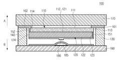
도 3은 본 발명의 일 실시예에 따른 전자제품에 있어서, 제 1실시예에 따른 표시장치를 도시한 단면도이다. 이하, 표시장치(100,200,300,400)의 두께방향으로 화면(171)과 가까워지는 방향을 제 1방향(A), 표시장치(100,200,300,400)의 두께방향으로 화면(171)과 멀어지는 방향을 제 2방향(B)으로 정의한다.3 is a cross-sectional view illustrating a display device according to a first embodiment in an electronic product according to an embodiment of the present invention. Hereinafter, the direction closer to the
도 3에 도시된 바와 같이, 표시장치(100)는 적어도 하나의 도광층(110,120)을 포함할 수 있다.3 , the
적어도 하나의 도광층(110,120)은 적어도 하나의 광원(130,140)으로부터 발산되는 광을 화면(171)의 전 영역에 걸쳐 균일하게 분산시켜주는 기능을 한다.The at least one
적어도 하나의 도광층(110,120)은 투광성 및 가요성(flexibility)을 가지는 재질로 형성될 수 있다. 일 예로써, 적어도 하나의 도광층(110,120)은 폴리카보네이트(PC), 폴리우레탄(PU), 폴리에틸렌 테레프탈레이트(PET) 및 폴리메타크릴산 메틸(PMMA) 중 적어도 하나의 재질을 포함할 수 있다.The at least one
적어도 하나의 도광층(110,120)은 제 1도광층(110) 및 제 2도광층(120)을 포함할 수 있다. 제 1도광층(110)은 표시장치(100)의 두께방향으로 제 2도광층(120)의 상부에 위치할 수 있다. 다시 말하면, 제 1도광층(110)은 제 1방향(A)을 향하고, 제 2도광층(120)은 제 2방향(B)을 향하도록 배치될 수 있다.The at least one
제 1도광층(110)은 화면(171)와 인접하도록 배치될 수 있다. 제 1도광층(110)에는 제 1이미지(510)(도4a참고)가 마련될 수 있다. 일 예로써, 제 1이미지(510)는 제 1도광층(110)의 제 2면(112) 상에 마련될 수 있다.The first
제 1도광층(110)은 제 1면(111), 제 2면(112), 제 3면(113) 및 제 4면(114)을 포함할 수 있다. 제 1면(111)은 제 1방향(A)을 향하고, 제 2면(112)은 제 2방향(B)을 향한다. 제 3면(113) 및 제 4면(114)은 제 1면(111) 및 제 2면(112) 사이에 위치한다. 제 3면(113) 및 제 4면(114)은 각각 광원(130,140)과 마주할 수 있다. 구체적으로, 제 3면(113)은 제 1광원(130)과 마주할 수 있고, 제 4면(114)은 제 2광원(140)과 마주할 수 있다.The first
제 2도광층(120)은 제 1도광층(110)을 사이에 두고 화면(171)과 마주하도록 배치될 수 있다. 다시 말하면, 제 2도광층(120)은 제 1도광층(110)을 사이에 두고 보호커버(170)와 마주하도록 배치될 수 있다.The second
제 2도광층(120)은 제 1면(121), 제 2면(122), 제 3면(123) 및 제 4면(124)을 포함할 수 있다. 제 1면(121)은 제 1방향(A)을 향하고, 제 2면(122)은 제 2방향(B)을 향한다. 제 3면(123) 및 제 4면(124)은 제 1면(121) 및 제 2면(122) 사이에 위치한다. 제 3면(123) 및 제 4면(124)은 각각 광원(130,140)과 마주할 수 있다. 구체적으로, 제 3면(123)은 제 1광원(130)과 마주할 수 있고, 제 4면(124)은 제 2광원(140)과 마주할 수 있다.The second
제 2도광층(120)은 적어도 하나의 광원(130,140)에서 발산되어 제 2도광층(120)으로 유입되는 광량이 적어도 하나의 광원(130,140)에서 발산되어 제 1도광층(110)으로 유입되는 광량보다 많도록 제 1도광층(110)보다 더 두꺼운 두께를 가질 수 있다. 구체적으로, 제 1도광층(110) 및 제 2도광층(120) 중 적어도 하나를 통과하여 화면(171)으로 발산되는 광의 밝기가 균일하도록 제 2도광층(120)은 제 1도광층(110)의 두께보다 25%이상 45%이하 더 두꺼운 두께를 가질 수 있다. 제 1광원(130)에서 발산된 광은 제 1도광층(110)을 통과하여 화면(171)으로 이동한다. 제 2광원(140)에서 발산된 광은 제 2도광층(120) 및 제 1도광층(110)을 차례로 통과하여 화면(171)으로 이동한다. 제 2광원(140)에서 발산된 광은 제 1도광층(110) 및 제 2도광층(120)을 통과하여 화면(171)으로 이동하기 때문에, 제 1도광층(110)을 통과하여 화면(171)으로 이동하는 제 1광원(130)에서 발산된 광에 비해 손실되는 광량이 많다. 따라서, 제 1광원(130)에서 발산된 광 및 제 2광원(140)에서 발산된 광의 밝기 내지 휘도가 균일하지 않을 수 있다. 이와 같은 문제점을 개선하기 위한 방안으로, 제 1도광층(110) 및 제 2도광층(120)의 두께를 상이하게 할 수 있다. 제 1도광층(110) 및 제 2도광층(120)의 두께차이에 대한 상세한 설명은 도 10에서 후술한다.In the second
적어도 하나의 도광층(110,120)의 개수는 두 개에 한정하지 않고, 다양하게 변경 가능하다.The number of the at least one
표시장치(100)는 적어도 하나의 광원(130,140)을 더 포함할 수 있다.The
적어도 하나의 광원(130,140)은 제 1도광층(110) 및 제 2도광층(120)에 선택적으로 조광(照光)할 수 있도록 배치될 수 있다.At least one
적어도 하나의 광원(130,140)은 발광 다이오드(Light Emitting Diode, LED) 및 일렉트로루미네센스(Electro-Luminescence, EL)를 포함할 수 있다.The at least one
적어도 하나의 광원(130,140)은 적어도 하나의 도광층(110,120)을 사이에 두고 서로 마주하도록 배치되는 제 1광원(130) 및 제 2광원(140)을 포함할 수 있다. 제 1광원(130)은 제 1도광층(110)의 제 3면(113) 및 제 2도광층(120)의 제 3면(123)과 마주할 수 있다. 제 2광원(140)은 제 1도광층(110)의 제 4면(114) 및 제 2도광층(120)의 제 4면(124)과 마주할 수 있다.The at least one
적어도 하나의 광원(130,140)에서 발산되는 광은 색(color)을 띨 수 있다.Light emitted from the at least one
표시장치(100)는 차광부(151,152)를 더 포함할 수 있다. 차광부(151,152)는 제 1광원(130) 및 제 2광원(140)에서 발산된 광이 각각 제 1도광층(110) 및 제 2도광층(120)의 내부로 유입될 수 있도록 제 1광원(130) 및 제 2광원(140)에서 발산되는 광의 이동을 가이드할 수 있다.The
차광부(151,152)는 제 1차광부(151) 및 제 2차광부(152)를 포함할 수 있다. 제 1차광부(151)는 제 1광원(130)에서 발산된 광이 제 1도광층(110)의 내부로 유입되도록 제 1광원(130) 및 제 2도광층(120) 사이에 마련될 수 있다. 다시 말하면, 제 1차광부(151)는 제 1광원(130)에서 발산된 광이 제 2도광층(120)의 내부로 유입되는 것을 차단할 수 있도록 제 2도광층(120)의 제 3면()에 마련될 수 있다. 제 2차광부(152)는 제 2광원(140)에서 발산된 광이 제 2도광층(120)의 내부로 유입되도록 제 2광원(140) 및 제 1도광층(110) 사이에 마련될 수 있다. 다시 말하면, 제 2차광부(152)는 제 2광원(140)에서 발산된 광이 제 1도광층(110)의 내부로 유입되는 것을 차단할 수 있도록 제 1도광층(110)의 제 4면(114)에 마련될 수 있다.The
표시장치(100)는 차광막(161,162)을 더 포함할 수 있다. 차광막(161,162)은 적어도 하나의광원(130,140)에서 발산된 광이 직접적으로 화면(171)으로 이동하는 것을 방지하도록 배치될 수 있다. 다시 말하면, 차광막(161,162)은 적어도 하나의 광원(130,140)에서 발산된 광이 적어도 하나의 도광층(110,120)을 거치지 않고 직접적으로 제 1방향(A)을 향하여 이동하는 것을 방지하도록 배치될 수 있다.The
차광막(161,162)은 적어도 하나의 광원(130,140)에서 발산된 광이 직접적으로 보호커버(170)로 이동하는 것을 방지하도록 보호커버(170) 및 적어도 하나의 광원(130,140) 사이에 배치될 수 있다.The
차광막(161,162)은 제 1차광막(161) 및 제 2차광막(162)을 포함할 수 있다. 제 1차광막(161)은 보호커버(170) 및 제 1광원(130) 사이에 배치될 수 있다. 제 1차광막(161)은 제 1방향(A)을 향하는 제 1광원(130)의 상면에 배치될 수 있다. 제 2차광막(162)은 보호커버(170) 및 제 2광원(140) 사이에 배치될 수 있다. 제 2차광막(162)은 제 1방향(A)을 향하는 제 2광원(140)의 상면에 배치될 수 있다.The light blocking layers 161 and 162 may include a first
서로 인접한 제 2차광막(162) 및 제 2차광부(152)는 일체로 형성될 수도 있다.The second
차광부(151,152) 및 차광막(161,162)은 차광테이프를 포함할 수 있다.The
표시장치(100)는 보호커버(170)를 더 포함할 수 있다.The
보호커버(170)의 표면에는 화면(171)이 형성될 수 있다. 보호커버(170)는 내 스크래치성을 가지는 재질로 형성될 수 있다. 일 예로써, 보호커버(170)는 폴리카보네이트(PC) 및 폴리에틸렌 테레프탈레이트(PET) 중 적어도 하나의 재질로 형성될 수 있다.A
보호커버(170)는 표시장치(100)의 두께방향으로 적어도 하나의 도광층(110,120) 상에 배치될 수 있다. 구체적으로, 보호커버(170)는 표시장치(100)의 두께방향으로 제 1도광층(110) 상에 배치될 수 있다.The
표시장치(100)는 인쇄회로기판(180)을 더 포함할 수 있다.The
인쇄회로기판(180)은 표시장치(100)의 두께방향으로 적어도 하나의 도광층(110,120)의 하부에 배치될 수 있다. 구체적으로, 인쇄회로기판(180)은 제 2도광층(120)과 마주하도록 배치될 수 있다.The printed
인쇄회로기판(180)에는 제 1광원(130)에 전원을 공급하는 제 1전원공급경로(미도시) 및 제 2광원(140)에 전원을 공급하는 제 2전원공급경로(미도시)가 마련될 수 있다.A first power supply path (not shown) for supplying power to the first
표시장치(100)는 제 1광원(130) 및 제 2광원(140)의 온/오프를 선택적으로 조절할 수 있도록 배치되는 스위치(185)를 더 포함할 수 있다. 스위치(185)는 적어도 하나의 광원(130,140)이 제 1도광층(110) 및 제 2도광층(120)에 선택적으로 조광하여 제 1이미지(510) 및 제 2이미지(520)를 선택적으로 표시할 수 있도록 인쇄회로기판(180)에 전기적 신호를 전달할 수 있다. 다시 말하면, 스위치(185)는 인쇄회로기판(180)에 마련되는 제 1전원공급경로 및 제 2전원공급경로를 선택적으로 연결 또는 차단할 수 있다.The
일 예로써, 스위치(185)는 돔 스위치를 포함할 수 있으나, 이에 한정하지 않는다. 이하, 돔 스위치가 적용된 표시장치(100)를 중심으로 설명한다.As an example, the
스위치(185)는 인쇄회로기판(180) 상에 마련될 수 있다. 스위치(185)는 제 2도광층(120)에 마련되는 가압부(186)에 의해 선택적으로 가압될 수 있다. 가압부(186)는 스위치(185)를 선택적으로 가압할 수 있도록 스위치(185)를 향하여 돌출될 수 있다. 구체적으로, 가압부(186)는 스위치(185)를 향하여 돌출되도록 제 2도광층(120)의 제 2면(122)에 마련될 수 있다. 또는, 가압부(186)는 스위치(185)를 향하여 돌출되도록 반사층(190)의 일 면에 마련될 수 있다.The
표시장치(100)는 서로 선택적으로 표시되는 복수의 이미지(510,520)를 더 포함할 수 있다. 복수의 이미지(510,520)는 제 1이미지(510) 및 제 2이미지(520)를 포함할 수 있다. 제 1이미지(510) 및 제 2이미지(520)는 서로 상이할 수 있다. 제 1이미지(510) 및 제 2이미지(520)에 대한 상세한 설명은 후술한다.The
도 4a는 본 발명의 일 실시예에 따른 전자제품에 있어서, 제 1실시예에 따른 표시장치에 형성된 제 1이미지를 도시한 도면이고, 도 4b는 본 발명의 일 실시예에 따른 전자제품에 있어서, 제 1실시예에 따른 표시장치에 형성된 제 2이미지를 도시한 도면이다. 도 4c는 본 발명의 일 실시예에 따른 전자제품에 있어서, 제 1실시예에 따른 표시장치에 형성된 제 1이미지 및 제 2이미지의 배치관계를 도시한 도면이다. 이하, 미도시된 도면부호는 도 3을 참조한다.4A is a view illustrating a first image formed on a display device according to the first embodiment in an electronic product according to an embodiment of the present invention, and FIG. 4B is an electronic product according to an embodiment of the present invention. , is a view showing a second image formed on the display device according to the first embodiment. 4C is a diagram illustrating an arrangement relationship between a first image and a second image formed on a display device according to the first embodiment in an electronic product according to an embodiment of the present invention. Hereinafter, reference numerals (not shown) refer to FIG. 3 .
도 4a에 도시된 바와 같이, 제 1이미지(510)는 제 1도광층(110)에 마련될 수 있다. 제 1이미지(510)는 제 1도광층(110)의 제 1면(111) 및 제 2면(112) 중 적어도 하나에 마련될 수 있다. 제 1이미지(510)는 제 1도광층(110)의 제 1면(111) 및 제 2면(112) 중 적어도 하나에 인쇄될 수 있다. 일 예로써, 제 1이미지(510)는 레이저 에칭(laser etching)을 통해 제 1도광층(110) 상에 인쇄될 수 있다. 또한, 제 1이미지(510)는 내부에서 광을 전파할 수 있는 투명 또는 반투명의 합성수지층 및 접착층 중 적어도 하나의 층에 마련될 수 있다. 이 경우, 제 1이미지(510)가 마련된 합성수지층 및 접착층 중 적어도 하나의 층은 제 1도광층(110) 상에 위치할 수 있다.As shown in FIG. 4A , the
도 4b에 도시된 바와 같이, 제 2이미지(520)는 제 2도광층(120) 및 반사층(190)(도5참고)의 사이에 마련될 수 있다. 제 2이미지(520)는 제 2도광층(120) 및 반사층(190) 중 적어도 하나에 마련될 수 있다. 제 2이미지(520)는 제 2도광층(120)의 제 1면(121), 제 2도광층(120)의 제 2면(122) 및 반사층(190) 중 적어도 하나에 인쇄될 수 있다. 일 예로써, 제 2이미지(520)는 레이저 에칭(laser etching)을 통해 제 2도광층(120)의 제 1면(121), 제 2도광층(120)의 제 2면(122) 및 반사층(190) 중 적어도 하나에 인쇄될 수 있다. 또한, 제 2이미지(520)는 내부에서 광을 전파할 수 있는 투명 또는 반투명의 합성수지층 및 접착층 중 적어도 하나의 층에 마련될 수 있다. 이 경우, 제 2이미지(520)가 마련된 합성수지층 및 접착층 중 적어도 하나의 층은 제 2도광층(120) 및 반사층(190) 중 적어도 하나의 층 상에 위치할 수 있다.As shown in FIG. 4B , the
도 4c에 도시된 바와 같이, 제 1이미지(510) 및 제 2이미지(520)는 표시장치(100)의 두께방향으로 서로 겹치도록 마련될 수 있다. 다시 말하면, 제 1이미지(510) 및 제 2이미지(520)는 제 1이미지(510)의 중심과 제 2이미지(520)의 중심이 거의 일치하도록 마련될 수 있다. 이와 같은 이미지 배치구조를 통해 좁은 영역에 복수의 이미지(510,520)를 선택적으로 표시하는 것이 가능하다. 따라서, 복수의 이미지(510,520)를 효율적으로 배치할 수 있다.As shown in FIG. 4C , the
또한, 제 1이미지(510) 및 제 2이미지(520)는 표시장치(100)의 두께방향으로 서로 어긋나도록 마련될 수도 있다. 다시 말하면, 제 1이미지(510) 및 제 2이미지(520)는 제 1이미지(510)의 중심과 제 2이미지(520)의 중심이 어긋나도록 마련될 수도 있다.Also, the
또한, 제 1이미지(510) 및 제 2이미지(520)는 표시장치(100)의 두께방향으로 일부만 겹치도록 마련될 수도 있다.Also, the
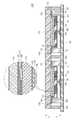
도 5는 도 4c의 I-I'선으로 절개한 제 1이미지 및 제 2이미지를 반영하여 제 1실시예에 따른 표시장치의 일부를 확대하여 도시한 도면이다. 이하, 미도시된 도면부호는 도 3 내지 도 4c를 참조한다.FIG. 5 is an enlarged view of a part of the display device according to the first embodiment by reflecting the first image and the second image cut along the line I-I' of FIG. 4C. Hereinafter, reference numerals (not shown) refer to FIGS. 3 to 4C .
도 5에 도시된 바와 같이, 표시장치(100)는 반사층(190)을 더 포함할 수 있다.5 , the
반사층(190)은 적어도 하나의 광원(130,140)에서 제 2도광층(120)의 내부로 발산된 광이 화면(171)을 향하여 이동할 수 있도록 제 2도광층(120)을 사이에 두고 제 1도광층(110)과 마주하도록 배치될 수 있다.The
표시장치(100)는 광투과층(192,194)을 더 포함할 수 있다.The
광투과층(192,194)은 제 1광투과층(192) 및 제 2광투과층(194)을 포함할 수 있다.The light transmitting layers 192 and 194 may include a first
제 1광투과층(192)은 제 1도광층(110) 및 제 1이미지(510) 사이에 마련될 수 있다. 제 1광투과층(192)은 제 1도광층(110)에 제 1이미지(510)가 마련됨에 따라 발생할 수 있는 단차를 방지할 수 있다. 제 1광투과층(192)은 제 1도광층(110) 상에 인쇄될 수 있다. 구체적으로, 제 1광투과층(192)은 제 1도광층(110)의 제 2면(112) 상에 인쇄될 수 있다. 제 1이미지(510) 및 제 1광투과층(192)은 서로 다른 광 굴절률을 가질 수 있다. 제 1광투과층(192)에서의 광 굴절률은 제 1이미지(510)에서의 광 굴절률보다 작을 수 있다.The first
제 2광투과층(194)은 제 2도광층(120) 및 반사층(190) 사이에 마련될 수 있다. 제 2광투과층(194)은 제 2도광층(120) 및 반사층(190) 사이에 제 2이미지(520)가 마련됨에 따라 발생할 수 있는 단차를 방지할 수 있다. 제 2광투과층(194)은 제 2도광층(120) 및 반사층(190) 중 적어도 하나의 층 상에 인쇄될 수 있다. 구체적으로, 제 2광투과층(194)은 제 2도광층(120)의 제 2면(122) 및 반사층(190) 중 적어도 하나에 인쇄될 수 있다. 제 2이미지(520) 및 제 2광투과층(194)은 서로 다른 광 굴절률을 가질 수 있다. 제 2광투과층(194)에서의 광 굴절률은 제 2이미지(520)에서의 광 굴절률보다 작을 수 있다.The second
표시장치(100)는 마스크층(195)을 더 포함할 수 있다.The
마스크층(195)은 제 1도광층(110) 및 제 2도광층(120)의 사이에 배치될 수 있다.The
마스크층(195)은 제 1도광층(110)의 제 2면(112) 및 제 2도광층(120)의 제 1면(121) 중 적어도 하나에 배치될 수 있다. 일 예로써, 마스크층(195)은 도 5에 도시된 바와 같이, 제 1이미지(510)와 마주하도록 제 2도광층(120)의 제 1면(121) 상에 마련될 수 있다.The
마스크층(195)은 일 예로써, 차광테이프일 수 있다. 마스크층(195)의 재질은 광을 차단할 수 있으면 충분하고, 차광테이프에 한정하지 않는다. 마스크층(195)의 적어도 일 면에는 점착층 내지 접착층이 형성될 수 있다. 마스크층(195)은 표시장치(100)의 두께방향으로 마스크층(195)의 하부에 위치하는 일부 구성들이 화면(171)을 통해 보이지 않도록 하고, 화면(171)에 표시되는 이미지의 시인성을 향상시키는 역할을 할 수 있다. 또한, 마스크층(195)은 제 1광원(130)에서 발산되어 제 1도광층(110)으로 유입된 광이 제 2방향(B)으로 이동하는 것을 방지할 수 있다.The
마스크층(195)은 제 2이미지(520)가 화면(171)에 표시될 수 있도록 제 1도광층(110)의 제 2면(112) 및 제 2도광층(120)의 제 1면(121) 중 적어도 하나의 일부에 배치될 수 있다. 마스크층(195)이 제 1도광층(110)의 제 2면(112) 및 제 2도광층(120)의 제 1면(121) 중 적어도 하나의 전부에 배치될 경우, 제 2광원(140)에서 발산되어 제 2도광층(120)으로 유입된 광은 제 1방향(A)을 향하여 이동하는 과정에서 차단된다. 따라서, 제 2이미지(520)는 화면(171) 상에 표시될 수 없다.The
제 2도광층(120)에는 요철구조(196)가 형성될 수 있다. 구체적으로, 요철구조(196)는 제 2도광층(120)의 제 1면(121)에 형성될 수 있다. 도 5에 도시된 바와 같이, 제 2도광층(120)의 제 1면(121)은 제 1이미지(510)와 마주할 수 있다. 요철구조(196)는 제 1도광층(110)으로 유입되어 화면(171)으로 발산되는 광과 제 2도광층(120)으로 유입되어 화면(171)으로 발산되는 광의 밝기 내지 휘도가 균일하도록 제 2도광층(120)으로 유입되어 화면(171)을 향하여 이동하는 광의 굴절률을 변화시킬 수 있다. 다시 말하면, 요철구조(196)는 제 2광원(140)에서 발산되어 제 2도광층(120)으로 유입된 광을 산란시킬 수 있다.A concave-
요철구조(196)는 프레스(press) 가공 및 레이저(laser) 가공 중 적어도 하나에 의해 형성될 수 있다.The
요철구조(196)는 제 2도광층(120)의 제 1면(121) 중 마스크층(195)과 마주하지 않는 부분에 형성될 수 있다.The
표시장치(100)는 칼라필터층(미도시)을 더 포함할 수 있다.The
칼라필터층은 적어도 하나의 광원(130,140)에서 발산된 광이 화면(171)을 향하여 이동하는 경로상에 배치될 수 있다.The color filter layer may be disposed on a path through which the light emitted from the at least one
칼라필터층은 염색법, 전착법, 안료분산법 및 인쇄법 등과 같은 다양한 방법으로 제조 가능하다.The color filter layer may be manufactured by various methods such as a dyeing method, an electrodeposition method, a pigment dispersion method, and a printing method.
칼라필터층은 투광성을 가질 수 있다.The color filter layer may have light-transmitting properties.
도 6은 본 발명의 일 실시예에 따른 전자제품에 있어서, 제 2실시예에 따른 표시장치를 도시한 단면도이다. 이하, 표시장치(100,200,300,400)의 두께방향으로 화면(171)과 가까워지는 방향을 제 1방향(A), 표시장치(100,200,300,400)의 두께방향으로 화면(171)과 멀어지는 방향을 제 2방향(B)으로 정의한다. 이하, 도 3 내지 도 5와 중복되는 설명은 생략할 수 있다. 이하, 미도시된 도면부호는 도 3 내지 도 5를 참조한다.6 is a cross-sectional view illustrating a display device according to a second embodiment in an electronic product according to an embodiment of the present invention. Hereinafter, the direction closer to the
도 6에 도시된 바와 같이, 표시장치(200)는 터치유닛(touch unit)(600)을 더 포함할 수 있다.As shown in FIG. 6 , the
터치유닛(600)을 가지는 전자제품은 화면(171)에 사용자의 손 또는 물체가 터치되면, 터치 위치 및 위치 변화를 인식하고 위치 변화에 대응하는 제스처를 확인하며, 터치 위치에 대응하는 동작 명령이나 제스처에 대응하는 동작 명령을 확인한 후 확인된 동작 명령에 대응하는 기능을 수행하고 기능 수행에 대한 영상을 표시한다.When the user's hand or an object is touched on the
터치유닛(600)은 제 1도광층(110)을 사이에 두고 제 2도광층(120)과 마주하도록 배치되고, 적어도 하나의 광원(130,140)이 제 1도광층(110) 및 제 2도광층(120)을 선택적으로 조광하여 제 1이미지(510) 및 제 2이미지(520)를 선택적으로 표시할 수 있도록 인쇄회로기판(180)에 전기적으로 연결될 수 있다.The
터치유닛(600)은 보호패널(610), 차단층(620), 제 1간극부(630), 터치패널(640) 및 제 2간극부(650)를 포함할 수 있다.The
보호패널(610)은 폴리카보네이트(PC) 및 폴리에틸렌 테레프탈레이트(PET) 중 적어도 하나를 포함하는 고분자 필름 또는 기판일 수 있다. 또는, 보호패널(610)은 유리(glass)판일 수 있다.The
보호패널(610)은 내 스크래치성을 가질 수 있다.The
보호패널(610)의 표면에는 화면(171)이 형성될 수 있다.A
터치패널(640)은 적어도 하나의 광원(130,140) 및 적어도 하나의 도광층(110,120)에 인접하도록 배치되고, 사용자에 의해 화면(171)이 터치되면 터치 신호를 출력하는 역할을 한다. 다시 말하면, 터치패널(640)은 표시장치(200)의 두께방향으로 적어도 하나의 광원(130,140) 및 적어도 하나의 도광층(110,120)의 상부에 배치될 수 있다.The
제 1간극부(630)는 보호패널(610) 및 터치패널(640)의 사이에 배치될 수 있다. 구체적으로, 제 1간극부(630)는 차단층(620) 및 터치패널(640)의 사이에 배치될 수 있다. 제 1간극부(630)는 내부에 광학용 투명 점착제(Optical clear adhesive, OCA)가 형성될 수 있다.The
제 2간극부(650)는 표시장치(200)의 두께방향으로 터치패널(640)의 하부에 배치될 수 있다. 다시 말하면, 제 2간극부(650)는 적어도 하나의 광원(130,140) 및 적어도 하나의 도광층(110,120) 중 적어도 하나와 터치패널(640)의 사이에 배치될 수 있다. 제 2간극부(650)는 에어갭으로 형성되거나, 내부에 광학용 투명 점착제가 형성될 수 있다.The
여기서 광학용 투명 점착제는 아크릴계 수지, 실리콘계 수지, 스티렌계 수지, 폴리에스테르계 수지, 고무계 수지 및 우레탄계 수지 중 적어도 하나를 포함하는 점착제 조성물로부터 형성될 수 있다.Here, the optically transparent pressure-sensitive adhesive may be formed from a pressure-sensitive adhesive composition including at least one of an acrylic resin, a silicone-based resin, a styrene-based resin, a polyester-based resin, a rubber-based resin, and a urethane-based resin.
차단층(620)은 보호패널(610) 및 제 1간극부(630)의 사이에 배치될 수 있다. 차단층(620)은 표시장치(200)의 두께방향으로 차단층(620) 하부에 위치하는 일부 구성들이 보이지 않도록 한다. 차단층(620)은 제 1이미지(510) 및 제 2이미지(520)가 화면(171) 상에 표시되는 것을 방해하지 않도록 배치될 수 있다.The
적어도 하나의 광원(130,140) 및 제 2간극부(650)의 사이에는 차광막(161,162)(도3참고)이 배치될 수 있다. 차광막(161,162)은 적어도 하나의 광원(130,140)에서 발산된 광이 직접적으로 터치유닛(600)으로 이동하는 것을 방지하도록 배치될 수 있다. 차광막(161,162)은 적어도 하나의 광원(130,140)에서 발산된 광이 적어도 하나의 도광층(110,120)을 거치지 않고 직접적으로 제 1방향(A)을 향하여 이동하는 것을 방지하도록 배치될 수 있다.Light blocking
터치유닛(600)은 연성회로기판(660)을 더 포함할 수 있다.The
연성회로기판(660)은 터치패널(640)에서 발생한 터치신호를 인쇄회로기판(180)에 전달하는 역할을 한다. 연성회로기판(660)은 터치패널(640) 및 인쇄회로기판(180)을 연결할 수 있다.The
도 7은 도 8c의 K-K'선으로 절개한 제 1이미지들 및 제 2이미지들을 반영하여 제 3실시예에 따른 표시장치를 도시한 단면도이고, 도 8a는 본 발명의 일 실시예에 따른 전자제품에 있어서, 제 3실시예에 따른 표시장치에 형성된 제 1이미지들을 도시한 도면이다. 도 8b는 본 발명의 일 실시예에 따른 전자제품에 있어서, 제 3실시예에 따른 표시장치에 형성된 제 2이미지들을 도시한 도면이고, 도 8c는 본 발명의 일 실시예에 따른 전자제품에 있어서, 제 3실시예에 따른 표시장치에 형성된 제 1이미지들 및 제 2이미지들의 배치관계를 도시한 도면이다. 이하, 제 1이미지들(510) 및 제 2이미지들(520)은 선택적으로 화면(171) 상에 표시될 수 있다. 다시 말하면, 제 1이미지들(510) 및 제 2이미지들(520)은 서로 전환 가능하도록 화면(171) 상에 표시될 수 있다. 이하, 표시장치(100,200,300,400)의 두께방향으로 화면(171)과 가까워지는 방향을 제 1방향(A), 표시장치(100,200,300,400)의 두께방향으로 화면(171)과 멀어지는 방향을 제 2방향(B)으로 정의한다. 이하, 도 3 및 도 5와 중복되는 설명은 생략할 수 있다.7 is a cross-sectional view illustrating a display device according to a third embodiment by reflecting the first images and the second images cut along the line K-K' of FIG. 8C, and FIG. 8A is a cross-sectional view according to an embodiment of the present invention. It is a diagram illustrating first images formed on a display device according to a third embodiment of an electronic product. 8B is a diagram illustrating second images formed on a display device according to a third embodiment in an electronic product according to an embodiment of the present invention, and FIG. 8C is an electronic product according to an embodiment of the present invention. , is a diagram illustrating an arrangement relationship of first images and second images formed in the display device according to the third embodiment. Hereinafter, the
도 7에 도시된 바와 같이, 표시장치(300)는 복수의 이미지 구현부(310)를 포함할 수 있다.As shown in FIG. 7 , the
복수의 이미지 구현부(310)는 서로 선택적으로 표시되는 복수의 이미지(510,520), 복수의 이미지(510,520)가 마련되는 적어도 하나의 도광층(110,120) 및 적어도 하나의 도광층(110,120)에 광을 조사할 수 있도록 마련되는 적어도 하나의 광원(130,140)을 포함할 수 있다.The plurality of
복수의 이미지(510,520)는 제 1이미지들(510) 및 제 2이미지들(520)을 포함할 수 있다. 복수의 이미지(510,520)는 서로 상이할 수 있다. 복수의 이미지(510,520)에 대한 상세한 설명은 후술한다.The plurality of
적어도 하나의 도광층(110,120)은 적어도 하나의 광원(130,140)으로부터 발산되는 광을 화면(171)의 전 영역에 걸쳐 균일하게 분산시켜주는 기능을 한다. 적어도 하나의 도광층(110,120)은 제 1도광층(110) 및 제 2도광층(120)을 포함할 수 있다.The at least one
적어도 하나의 도광층(110,120)에 대한 설명은 도 3 및 도 5에서 설명한 것과 동일한 바, 생략한다.A description of the at least one
제 2도광층(120)은 적어도 하나의 광원(130,140)에서 발산되어 제 2도광층(120)으로 유입되는 광량이 적어도 하나의 광원(130,140)에서 발산되어 제 1도광층(110)으로 유입되는 광량보다 많도록 제 1도광층(110)보다 더 두꺼운 두께를 가질 수 있다. 구체적으로, 제 1도광층(110) 및 제 2도광층(120) 중 적어도 하나를 통과하여 화면(171)으로 발산되는 광의 밝기가 균일하도록 제 2도광층(120)은 제 1도광층(110)의 두께보다 25%이상 45%이하 더 두꺼운 두께를 가질 수 있다. 제 1광원(130)에서 발산된 광은 제 1도광층(110)을 통과하여 화면(171)으로 이동한다. 제 2광원(140)에서 발산된 광은 제 2도광층(120) 및 제 1도광층(110)을 차례로 통과하여 화면(171)으로 이동한다. 제 2광원(140)에서 발산된 광은 제 1도광층(110) 및 제 2도광층(120)을 통과하여 화면(171)으로 이동하기 때문에, 제 1도광층(110)을 통과하여 화면(171)으로 이동하는 제 1광원(130)에서 발산된 광에 비해 손실되는 광량이 많다. 따라서, 제 1광원(130)에서 발산된 광 및 제 2광원(140)에서 발산된 광의 밝기 내지 휘도가 균일하지 않을 수 있다. 이와 같은 문제점을 개선하기 위한 방안으로, 제 1도광층(110) 및 제 2도광층(120)의 두께를 상이하게 할 수 있다. 제 1도광층(110) 및 제 2도광층(120)의 두께차이에 대한 상세한 설명은 도 10에서 후술한다.In the second
적어도 하나의 광원(130,140)은 제 1도광층(110) 및 제 2도광층(120)에 선택적으로 조광(照光)할 수 있도록 배치될 수 있다. 적어도 하나의 광원(130,140)은 제 1광원(130) 및 제 2광원(140)을 포함할 수 있다. 적어도 하나의 광원(130,140)에 대한 설명은 도 3 및 도 5에서 설명한 것과 동일한 바, 생략한다.At least one
표시장치(300)는 차광부(151,152)를 더 포함할 수 있다. 차광부(151,152)는 제 1광원(130) 및 제 2광원(140)에서 발산된 광이 각각 제 1도광층(110) 및 제 2도광층(120)의 내부로 유입될 수 있도록 제 1광원(130) 및 제 2광원(140)에서 발산되는 광의 이동을 가이드할 수 있다. 차광부(151,152)는 제 1차광부(151) 및 제 2차광부(152)를 포함할 수 있다. 차광부(151,152)에 대한 설명은 도 3 및 도 5에서 설명한 것과 동일한 바, 생략한다.The
표시장치(300)는 차광막(161,162)을 더 포함할 수 있다. 차광막(161,162)은 적어도 하나의 광원(130,140)에서 발산된 광이 직접적으로 화면(171)으로 이동하는 것을 방지하도록 배치될 수 있다. 다시 말하면, 차광막(161,162)은 적어도 하나의 광원(130,140)에서 발산된 광이 적어도 하나의 도광층(110,120)을 거치지 않고 직접적으로 제 1방향(A)을 향하여 이동하는 것을 방지하도록 배치될 수 있다. 차광막(161,162)은 제 1차광막(161) 및 제 2차광막(162)을 포함할 수 있다. 차광막(161,162)에 대한 설명은 도 3 및 도 5에서 설명한 것과 동일한 바, 생략한다.The
표시장치(300)는 보호커버(170)를 더 포함할 수 있다. 보호커버(170)에 대한 설명은 도 3 및 도 5에서 설명한 것과 동일한 바, 생략한다.The
표시장치(300)는 인쇄회로기판(180)을 더 포함할 수 있다. 인쇄회로기판(180)은 복수의 이미지 구현부(310) 및 차광부(151,152)를 사이에 두고 화면(171)과 마주하도록 배치될 수 있다. 복수의 이미지 구현부(310) 및 차광부(151,152)는 인쇄회로기판(180) 상에 배치될 수 있다.The
표시장치(300)는 제 1광원(130) 및 제 2광원(140)의 온/오프를 선택적으로 조절할 수 있도록 배치되는 스위치(185)를 더 포함할 수 있다. 스위치(185)에 대한 설명은 도 3 및 도 5에서 설명한 것과 동일한 바, 생략한다. 스위치(185)의 개수 및 위치는 복수의 이미지 구현부(310)의 개수 및 위치에 대응할 수 있다.The
표시장치(300)는 차광부(320)를 더 포함할 수 있다.The
차광부(320)는 복수의 이미지 구현부(310) 중 어느 하나의 광원(130,140)에서 발산되는 광 및 복수의 이미지 구현부(310) 중 다른 하나의 광원(130,140)에서 발산되는 광이 서로 간섭되는 것을 방지하도록 복수의 이미지 구현부(310)의 경계를 형성할 수 있다.The
차광부(320)는 복수의 이미지 구현부(310)의 사이에 배치될 수 있다. 구체적으로, 차광부(320)는 서로 인접하는 복수의 이미지 구현부(310)의 사이에 배치될 수 있다.The
차광부(320)는 복수의 이미지 구현부(310) 각각의 둘레를 따라 배치될 수 있다.The
차광부(320)는 복수의 이미지 구현부(310)의 경계를 형성하도록 보호커버(170) 및 인쇄회로기판(180) 사이에 배치될 수 있다.The
차광부(320)는 보호커버(170) 및 인쇄회로기판(180) 중 적어도 하나에 연결될 수 있다.The
차광부(320)는 보호커버(170) 및 인쇄회로기판(180) 중 적어도 하나와 일체로 형성될 수 있다.The
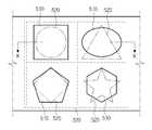
도 8a에 도시된 바와 같이, 제 1이미지들(510)은 제 1도광층(110)에 마련될 수 있다. 제 1이미지들(510)은 제 1도광층(110)의 제 1면(111) 및 제 2면(112) 중 적어도 하나에 마련될 수 있다. 제 1이미지들(510)은 제 1도광층(110)의 제 1면(111) 및 제 2면(112) 중 적어도 하나에 인쇄될 수 있다. 일 예로써, 제 1이미지들(510)은 레이저 에칭(laser etching)을 통해 제 1도광층(110) 상에 인쇄될 수 있다. 또한, 제 1이미지들(510)은 내부에서 광을 전파할 수 있는 투명 또는 반투명의 합성수지층 및 접착층 중 적어도 하나의 층에 마련될 수 있다. 이 경우, 제 1이미지들(510)이 마련된 합성수지층 및 접착층 중 적어도 하나의 층은 제 1도광층(110) 상에 위치할 수 있다.As shown in FIG. 8A , the
도 8b에 도시된 바와 같이, 제 2이미지들(520)은 제 2도광층(120) 및 반사층(190)의 사이에 마련될 수 있다. 제 2이미지들(520)은 제 2도광층(120) 및 반사층(190) 중 적어도 하나에 마련될 수 있다. 제 2이미지들(520)은 제 2도광층(120)의 제 1면(121), 제 2도광층(120)의 제 2면(122) 및 반사층(190) 중 적어도 하나에 인쇄될 수 있다. 일 예로써, 제 2이미지들(520)은 레이저 에칭(laser etching)을 통해 제 2도광층(120)의 제 1면(121), 제 2도광층(120)의 제 2면(122) 및 반사층(190) 중 적어도 하나에 인쇄될 수 있다. 또한, 제 2이미지들(520)은 내부에서 광을 전파할 수 있는 투명 또는 반투명의 합성수지층 및 접착층 중 적어도 하나의 층에 마련될 수 있다. 이 경우, 제 2이미지들(520)이 마련된 합성수지층 및 접착층 중 적어도 하나의 층은 제 2도광층(120) 및 반사층(190) 중 적어도 하나의 층 상에 위치할 수 있다.As shown in FIG. 8B , the
도 8c에 도시된 바와 같이, 제 1이미지들(510) 및 제 2이미지들(520)은 표시장치(300)의 두께방향으로 서로 겹치도록 마련될 수 있다. 다시 말하면, 제 1이미지들(510) 및 제 2이미지들(520)은 제 1이미지들(510) 각각의 중심과 제 2이미지들(520)의 각각의 중심이 거의 일치하도록 마련될 수 있다. 이와 같은 이미지 배치구조를 통해 좁은 영역에 복수의 이미지(510,520)를 선택적으로 표시하는 것이 가능하다. 따라서, 복수의 이미지(510,520)를 효율적으로 배치할 수 있다.As shown in FIG. 8C , the
또한, 제 1이미지들(510) 및 제 2이미지들(520)은 표시장치(300)의 두께방향으로 서로 어긋나도록 마련될 수도 있다. 다시 말하면, 제 1이미지들(510) 및 제 2이미지들(520)은 제 1이미지들(510) 각각의 중심과 제 2이미지들(520)의 각각의 중심이 어긋나도록 마련될 수도 있다.Also, the
또한, 제 1이미지들(510) 및 제 2이미지들(520)은 표시장치(300)의 두께방향으로 일부만 겹치도록 마련될 수도 있다.Also, the
도 9는 본 발명의 일 실시예에 따른 전자제품에 있어서, 제 4실시예에 따른 표시장치를 도시한 단면도이다. 이하, 표시장치(100,200,300,400)의 두께방향으로 화면(171)과 가까워지는 방향을 제 1방향(A), 표시장치(100,200,300,400)의 두께방향으로 화면(171)과 멀어지는 방향을 제 2방향(B)으로 정의한다. 이하, 도 6 및 도 7 내지 도 8c와 중복되는 설명은 생략할 수 있다. 이하, 미도시된 도면부호는 도 7 내지 도 8c를 참조한다.9 is a cross-sectional view illustrating a display device according to a fourth embodiment in an electronic product according to an embodiment of the present invention. Hereinafter, the direction closer to the
도 9에 도시된 바와 같이, 표시장치(400)는 터치유닛(touch unit)(600)을 더 포함할 수 있다.As shown in FIG. 9 , the
터치유닛(600)은 복수의 이미지 구현부(310)를 사이에 두고 인쇄회로기판(180)과 마주하도록 배치되고, 적어도 하나의 광원(130,140)이 제 1도광층(110) 및 제 2도광층(120)을 선택적으로 조광하여 제 1이미지들(510) 및 제 2이미지들(520)을 선택적으로 표시할 수 있도록 인쇄회로기판(180)에 전기적으로 연결될 수 있다.The
터치유닛(600)은 보호패널(610), 차단층(620), 제 1간극부(630), 터치패널(640), 제 2간극부(650) 및 연성회로기판(660)을 포함할 수 있다. 터치유닛(600)에 대한 설명은 도 6에서 설명한 것과 동일한 바, 생략한다.The
도 10은 본 발명의 일 실시예에 따른 전자제품에 있어서, 제 1도광층 및 제 2도광층의 두께 비에 따른 광학품질의 균일성을 보여주는 표이다. 제 1도광층(110) 및 제 2도광층(120)의 두께단위는 마이크로미터(μm)이다. 제 1도광층(110) 및 제 2도광층(120)의 밝기단위는 칸델라(cd)이다.10 is a table showing the uniformity of optical quality according to a thickness ratio of a first light guide layer and a second light guide layer in an electronic product according to an embodiment of the present invention. The thickness unit of the first
도 10에 도시된 바와 같이, 제 2도광층(120)은 제 1도광층(110) 및 제 2도광층(120) 중 적어도 하나를 통과하여 화면(171)으로 발산되는 광의 밝기가 균일하도록 제 1도광층(110)의 두께보다 25%이상 45%이하 더 두꺼운 두께를 가질 수 있다.As shown in FIG. 10 , the second
제 1도광층(110)의 두께가 0.7 μm인 경우, 제 2도광층(120)이 0.9 μm이상 1.0 μm이하의 두께를 가질 때, 제 1도광층(110) 및 제 2도광층(120)의 밝기가 비슷하다. 즉, 제 2도광층(120)의 두께를 제 1도광층(110)의 두께 대비 25%이상 45%이하 증가시킬 경우, 제 1도광층(110) 및 제 2도광층(120) 중 적어도 하나를 통과하여 화면(171)으로 발산되는 광의 밝기가 균일하다.When the thickness of the first
이상에서는 특정의 실시예에 대하여 도시하고 설명하였다. 그러나, 상기한 실시예에만 한정되지 않으며, 발명이 속하는 기술분야에서 통상의 지식을 가진 자라면 이하의 청구범위에 기재된 발명의 기술적 사상의 요지를 벗어남이 없이 얼마든지 다양하게 변경 실시할 수 있을 것이다.In the above, specific embodiments have been shown and described. However, it is not limited only to the above-described embodiments, and those of ordinary skill in the art to which the invention pertains can make various changes without departing from the spirit of the invention described in the claims below. .
100,200,300,400 : 표시장치 10 : 세탁기
13 : 조작부 14 : 전원버튼
15 : 디스플레이부 20 : 조리기기
17 : 디스플레이부 18 : 조작부
110 : 제 1도광층 111 : 제 1면
112 : 제 2면 113 : 제 3면
114 : 제 4면 120 : 제 2도광층
121 : 제 1면 122 : 제 2면
123 : 제 3면 124 : 제 4면
130 : 제 1광원 140 : 제 2광원
151 : 제 1차광부 152 : 제 2차광부
161 : 제 1차광막 162 : 제 2차광막
170 : 보호커버 171 : 화면
180 : 인쇄회로기판 185 : 스위치
186 : 가압부 190 : 반사층
192 : 제 1광투과층 194 : 제 2광투과층
195 : 마스크층 196 : 요철구조
510 : 제 1이미지(들) 520 : 제 2이미지(들)
600 : 터치유닛 610 : 보호패널
620 : 차단층 630 : 제 1간극부
640 : 터치패널 650 : 제 2간극부
660 : 연성회로기판 310 : 이미지 구현부
320 : 차광부100,200,300,400: display device 10: washing machine
13: control unit 14: power button
15: display unit 20: cooking equipment
17: display unit 18: operation unit
110: first light guide layer 111: first surface
112: second side 113: third side
114: fourth surface 120: second light guide layer
121: first side 122: second side
123: third page 124: fourth page
130: first light source 140: second light source
151: first light-shielding unit 152: second light-shielding unit
161: first light-shielding film 162: second light-shielding film
170: protective cover 171: screen
180: printed circuit board 185: switch
186: pressing part 190: reflective layer
192: first light-transmitting layer 194: second light-transmitting layer
195: mask layer 196: concave-convex structure
510: first image(s) 520: second image(s)
600: touch unit 610: protection panel
620: blocking layer 630: first gap portion
640: touch panel 650: second gap
660: flexible circuit board 310: image realization unit
320: light blocking unit
Claims (22)
Translated fromKorean상기 표시장치는,
서로 선택적으로 표시되는 제 1이미지 및 제 2이미지와, 상기 제1이미지 및 제2이미지가 표시되는 화면과, 상기 화면과 인접하도록 배치되는 제 1도광층과, 상기 제 1도광층을 사이에 두고 상기 화면과 마주하도록 배치되는 제 2도광층과, 상기 제 1도광층 및 상기 제 2도광층에 선택적으로 조광할 수 있도록 배치되는 제1광원 및 제2광원을 포함하는 복수의 이미지 구현부;
상기 화면이 표면에 형성되고, 내 스크래치성을 가지도록 상기 제1도광층 상에 배치되는 보호커버;
상기 제1광원 및 제2광원에서 발산된 광이 각각 제1도광층 및 제2도광층의 내부러 유입될 수 있도록 광의 이동을 가이드하도록 마련되는 제1차광부 및 제2차광부; 및
상기 복수의 이미지 구현부 및 상기 제1및 제2차광부를 사이에 두고 상기 화면과 마주하도록 배치되는 인쇄회로기판;을 포함하고,
상기 적어도 하나의 광원에서 발산되어 상기 제 2도광층으로 유입되는 광량이 상기 적어도 하나의 광원에서 발산되어 상기 제 1도광층으로 유입되는 광량보다 많도록 상기 제 2도광층은 상기 제 1도광층의 두께보다 25%이상 45%이하 더 두꺼운 두께를 가지며,
상기 복수의 이미지 구현부 중 어느 하나의 광원에서 발산되는 광 및 상기 복수의 이미지 구현부 중 다른 하나의 광원에서 발산되는 광이 서로 간섭되는 것을 방지하도록 복수의 이미지 구현부의 사이 및 상기 보호커버 및 상기 인쇄회로기판 사이에 배치되는 차광부를 더 포함하는 것을 특징으로 하는 전자제품.In the electronic product having a display device for displaying a plurality of images,
The display device is
A first image and a second image selectively displayed to each other, a screen on which the first image and the second image are displayed, a first light guide layer disposed adjacent to the screen, and the first light guide layer interposed therebetween a plurality of image implementation units including a second light guide layer disposed to face the screen, and first and second light sources disposed to selectively dim the first light guide layer and the second light guide layer;
a protective cover formed on the surface of the screen and disposed on the first light guide layer to have scratch resistance;
a first light blocking unit and a second light blocking unit provided to guide the movement of light so that the light emitted from the first light source and the second light source can flow into the inside of the first light guide layer and the second light guide layer, respectively; and
a printed circuit board disposed to face the screen with the plurality of image implementation units and the first and second light blocking units interposed therebetween; and
The second light guiding layer is configured such that the amount of light emitted from the at least one light source and introduced into the second light guide layer is greater than the amount of light emitted from the at least one light source and introduced into the first light guide layer. It has a thickness that is 25% or more and 45% or less thicker than the thickness.
Between the plurality of image implementation units and the protective cover and the light emitted from any one light source of the plurality of image implementation units and the light emitted from the other light source of the plurality of image implementation units to prevent interference with each other Electronic product, characterized in that it further comprises a light blocking portion disposed between the printed circuit board.
상기 제1광원 및 제2광원은 상기 제 1도광층 및 상기 제 2도광층을 사이에 두고 서로 마주하도록 배치되는 것을 특징으로 하는 전자제품.The method of claim 1,
and the first light source and the second light source are disposed to face each other with the first light guide layer and the second light guide layer interposed therebetween.
상기 제1차광부는 상기 제 1광원에서 발산된 광이 상기 제 1도광층의 내부로 유입되도록 상기 제 1광원 및 상기 제 2도광층 사이에 마련되고,
상기 제2차광부는 상기 제 2광원에서 발산된 광이 상기 제 2도광층의 내부로 유입되도록 상기 제 2광원 및 상기 제 1도광층 사이에 마련되는 것을 특징으로 하는 전자제품.The method of claim 1,
The first light blocking part is provided between the first light source and the second light guide layer so that the light emitted from the first light source flows into the inside of the first light guide layer,
and the second light blocking part is provided between the second light source and the first light guide layer so that the light emitted from the second light source flows into the second light guide layer.
상기 제 2이미지는 상기 제 2도광층에 마련되는 것을 특징으로 하는 전자제품.The method of claim 1,
and the second image is provided on the second light guide layer.
상기 표시장치는 상기 적어도 하나의 광원에서 상기 제 2도광층의 내부로 발산된 광이 상기 화면을 향하여 이동할 수 있도록 상기 제 2도광층을 사이에 두고 상기 제 1도광층과 마주하도록 배치되는 반사층을 더 포함하고,
상기 제 2이미지는 상기 제 2도광층 및 상기 반사층의 사이에 마련되는 것을 특징으로 하는 전자제품.The method of claim 1,
The display device includes a reflective layer disposed to face the first light guiding layer with the second light guiding layer interposed therebetween so that light emitted from the at least one light source into the second light guiding layer can move toward the screen. including more,
The second image is provided between the second light guiding layer and the reflective layer.
상기 제 1이미지 및 상기 제 2이미지는 각각 상기 제 1도광층 및 상기 반사층 상에 레이저 에칭(laser etching)을 통해 인쇄되는 것을 특징으로 하는 전자제품.7. The method of claim 6,
and the first image and the second image are printed on the first light guiding layer and the reflective layer through laser etching, respectively.
상기 제 1이미지와 마주하는 상기 제 2도광층의 제 1면에는 상기 제 1도광층으로 유입되어 상기 화면으로 발산되는 광과 상기 제 2도광층으로 유입되어 상기 화면으로 발산되는 광의 밝기가 균일하도록 상기 제 2도광층으로 유입되어 상기 화면을 향하여 이동하는 광의 굴절률을 변화시키는 요철구조가 형성되는 것을 특징으로 하는 전자제품.The method of claim 1,
On the first surface of the second light guide layer facing the first image, the brightness of the light flowing into the first light guide layer and emitted to the screen and the light flowing into the second light guide layer and emitted to the screen are uniform. and a concave-convex structure for changing a refractive index of light flowing into the second light guide layer and moving toward the screen is formed.
상기 요철구조는 프레스 가공 및 레이저 가공 중 적어도 하나에 의해 형성되는 것을 특징으로 하는 전자제품.9. The method of claim 8,
The concave-convex structure is an electronic product, characterized in that formed by at least one of press processing and laser processing.
상기 표시장치는 표면에 상기 화면이 형성되고, 내 스크래치성을 가지도록 상기 제 1도광층 상에 배치되는 보호커버를 더 포함하는 것을 특징으로 하는 전자제품.The method of claim 1,
The display device is an electronic product, characterized in that the screen is formed on the surface, and further comprising a protective cover disposed on the first light guide layer to have scratch resistance.
상기 제 1도광층 및 상기 제 2도광층은 폴리카보네이트(PC), 폴리우레탄(PU), 폴리에틸렌 테레프탈레이트(PET) 및 폴리메타크릴산 메틸(PMMA) 중 적어도 하나의 재질을 포함하는 것을 특징으로 하는 전자제품.The method of claim 1,
The first light guiding layer and the second light guiding layer include at least one of polycarbonate (PC), polyurethane (PU), polyethylene terephthalate (PET), and polymethyl methacrylate (PMMA). electronics that do.
상기 표시장치는,
상기 제1광원 및 제2광원이 상기 제 1도광층 및 상기 제 2도광층에 선택적으로 조광하여 상기 제 1이미지 및 상기 제 2이미지를 선택적으로 표시할 수 있도록 상기 인쇄회로기판에 전기적 신호를 전달하는 돔 스위치;를 더 포함하는 것을 특징으로 하는 전자제품.The method of claim 1,
The display device is
The first light source and the second light source selectively dim the first light guide layer and the second light guide layer to transmit an electrical signal to the printed circuit board to selectively display the first image and the second image An electronic product comprising a dome switch that further comprises.
상기 돔 스위치는 상기 인쇄회로기판 상에 마련되고,
상기 제 2도광층에는 상기 돔 스위치를 선택적으로 가압할 수 있도록 상기 돔 스위치를 향하여 돌출되는 가압부가 마련되는 것을 특징으로 하는 전자제품.13. The method of claim 12,
The dome switch is provided on the printed circuit board,
The electronic product according to claim 1, wherein a pressing portion protruding toward the dome switch is provided on the second light guiding layer to selectively press the dome switch.
상기 표시장치는,
상기 제 1도광층을 사이에 두고 상기 제 2도광층과 마주하도록 배치되고, 상기 제1광원 및 제2광원이 상기 제 1도광층 및 상기 제 2도광층에 선택적으로 조광하여 상기 제 1이미지 및 상기 제 2이미지를 선택적으로 표시할 수 있도록 상기 인쇄회로기판에 전기적으로 연결되는 터치유닛;을 더 포함하는 것을 특징으로 하는 전자제품.The method of claim 1,
The display device is
It is disposed to face the second light guide layer with the first light guide layer interposed therebetween, and the first light source and the second light source selectively illuminate the first light guide layer and the second light guide layer to form the first image and and a touch unit electrically connected to the printed circuit board to selectively display the second image.
상기 표시장치는,
서로 선택적으로 표시되는 복수의 이미지, 상기 복수의 이미지가 표시되는 화면, 상기 복수의 이미지가 마련되는 적어도 하나의 도광층 및 상기 적어도 하나의 도광층에 광을 조사할 수 있도록 마련되는 적어도 하나의 광원을 포함하는 복수의 이미지 구현부;
표면에 상기 화면이 형성되고, 내 스크래치성을 가지도록 상기 적어도 하나의 도광층 상에 배치되는 보호커버;
상기 복수의 이미지 구현부 중 어느 하나의 광원에서 발산되는 광 및 상기 복수의 이미지 구현부 중 다른 하나의 광원에서 발산되는 광이 서로 간섭되는 것을 방지하도록 상기 복수의 이미지 구현부의 경계를 형성하는 차광부; 및
상기 복수의 이미지 구현부 및 상기 차광부를 사이에 두고 상기 화면과 마주하도록 배치되는 인쇄회로기판;
상기 차광부는, 상기 복수의 이미지 구현부 중 어느 하나의 광원에서 발산되는 광 및 상기 복수의 이미지 구현부 중 다른 하나의 광원에서 발산되는 광이 서로 간섭되는 것을 방지하도록 상기 복수의 이미지 구현부 각각의 둘레를 따라 배치되고, 상기 보호커버 및 상기 인쇄회로기판 중 적어도 하나에 연결될 수 있는 것을 특징으로 하는 전자제품.In an electronic product having a display device,
The display device is
A plurality of images selectively displayed with each other, a screen on which the plurality of images are displayed, at least one light guide layer on which the plurality of images are provided, and at least one light source provided to irradiate light to the at least one light guide layer a plurality of image implementations including;
a protective cover having the screen formed on the surface and disposed on the at least one light guide layer to have scratch resistance;
A light blocking unit forming a boundary between the plurality of image implementing units to prevent the light emitted from any one light source among the plurality of image implementing units and light emitted from the other light source among the plurality of image implementing units from interfering with each other ; and
a printed circuit board disposed to face the screen with the plurality of image implementation units and the light blocking unit interposed therebetween;
The light blocking unit is configured to prevent the light emitted from any one light source among the plurality of image implementation units and light emitted from the other light source among the plurality of image implementation units from interfering with each other. It is disposed along the periphery, the electronic product characterized in that it can be connected to at least one of the protective cover and the printed circuit board.
상기 적어도 하나의 도광층은,
상기 화면과 인접하도록 배치되고, 제 1이미지가 마련되는 제 1도광층; 및
상기 제 1도광층을 사이에 두고 상기 화면과 마주하도록 배치되고, 제 2이미지가 마련되는 제 2도광층;을 포함하고,
상기 제 2도광층은 상기 제 1도광층 및 상기 제 2도광층 중 적어도 하나를 통과하여 상기 화면으로 발산되는 광의 밝기가 균일하도록 상기 제 1도광층의 두께보다 25%이상 45%이하 더 두꺼운 두께를 가지는 것을 특징으로 하는 전자제품.16. The method of claim 15,
the at least one light guide layer,
a first light guide layer disposed adjacent to the screen and provided with a first image; and
a second light guide layer disposed to face the screen with the first light guide layer interposed therebetween and provided with a second image;
The second light guide layer is 25% or more and 45% or less thicker than the thickness of the first light guide layer so that the brightness of light emitted to the screen through at least one of the first light guide layer and the second light guide layer is uniform. Electronic products, characterized in that having a.
상기 적어도 하나의 광원은 상기 적어도 하나의 도광층을 사이에 두고 서로 마주하도록 배치되는 제 1광원 및 제 2광원을 포함하는 것을 특징으로 하는 전자제품.16. The method of claim 15,
The at least one light source includes a first light source and a second light source disposed to face each other with the at least one light guide layer interposed therebetween.
상기 표시장치는,
상기 적어도 하나의 광원이 상기 적어도 하나의 도광층에 선택적으로 조광할 수 있도록 상기 인쇄회로기판에 전기적으로 연결되는 돔 스위치;를 더 포함하는 것을 특징으로 하는 전자제품.16. The method of claim 15,
The display device is
and a dome switch electrically connected to the printed circuit board so that the at least one light source can selectively dim the at least one light guide layer.
상기 보호커버 및 상기 적어도 하나의 광원 사이에는 상기 적어도 하나의 광원에서 발산된 광이 직접적으로 상기 보호커버로 이동하는 것을 방지하도록 차광막이 배치되는 것을 특징으로 하는 전자제품.16. The method of claim 15,
An electronic product characterized in that a light blocking film is disposed between the protective cover and the at least one light source to prevent the light emitted from the at least one light source from moving directly to the protective cover.
상기 표시장치는,
상기 적어도 하나의 광원이 상기 적어도 하나의 도광층에 선택적으로 조광할 수 있도록 상기 인쇄회로기판에 전기적으로 연결되고, 표면에 상기 화면이 형성되는 터치유닛;을 더 포함하는 것을 특징으로 하는 전자제품.16. The method of claim 15,
The display device is
and a touch unit electrically connected to the printed circuit board so that the at least one light source can selectively dim the at least one light guide layer, the touch unit having the screen formed on a surface thereof.
Priority Applications (4)
| Application Number | Priority Date | Filing Date | Title |
|---|---|---|---|
| KR1020140187458AKR102293599B1 (en) | 2014-12-23 | 2014-12-23 | Electronic appliance |
| CN201510977764.0ACN105719576A (en) | 2014-12-23 | 2015-12-23 | electrical appliance |
| EP15202262.0AEP3038077B1 (en) | 2014-12-23 | 2015-12-23 | Electronic appliance |
| US14/757,665US9989694B2 (en) | 2014-12-23 | 2015-12-23 | Electronic appliance |
Applications Claiming Priority (1)
| Application Number | Priority Date | Filing Date | Title |
|---|---|---|---|
| KR1020140187458AKR102293599B1 (en) | 2014-12-23 | 2014-12-23 | Electronic appliance |
Publications (2)
| Publication Number | Publication Date |
|---|---|
| KR20160076869A KR20160076869A (en) | 2016-07-01 |
| KR102293599B1true KR102293599B1 (en) | 2021-08-26 |
Family
ID=55070755
Family Applications (1)
| Application Number | Title | Priority Date | Filing Date |
|---|---|---|---|
| KR1020140187458AActiveKR102293599B1 (en) | 2014-12-23 | 2014-12-23 | Electronic appliance |
Country Status (4)
| Country | Link |
|---|---|
| US (1) | US9989694B2 (en) |
| EP (1) | EP3038077B1 (en) |
| KR (1) | KR102293599B1 (en) |
| CN (1) | CN105719576A (en) |
Families Citing this family (3)
| Publication number | Priority date | Publication date | Assignee | Title |
|---|---|---|---|---|
| JP2019184817A (en)* | 2018-04-10 | 2019-10-24 | オムロン株式会社 | Operating device |
| EP3628919B1 (en)* | 2018-09-27 | 2023-02-22 | BSH Hausgeräte GmbH | Device and method for displaying optical information |
| CN111708215A (en)* | 2020-07-14 | 2020-09-25 | 京东方科技集团股份有限公司 | A mirror switching screen and display device |
Citations (1)
| Publication number | Priority date | Publication date | Assignee | Title |
|---|---|---|---|---|
| KR100976975B1 (en)* | 2010-04-01 | 2010-08-23 | 주식회사 유스테크 | Overap keypad |
Family Cites Families (32)
| Publication number | Priority date | Publication date | Assignee | Title |
|---|---|---|---|---|
| GB1507725A (en)* | 1974-08-30 | 1978-04-19 | Toyota Motor Co Ltd | Indicator device for automobiles |
| US5926601A (en)* | 1996-05-02 | 1999-07-20 | Briteview Technologies, Inc. | Stacked backlighting system using microprisms |
| DE29801008U1 (en)* | 1998-01-23 | 1998-03-12 | Erco Leuchten | Luminaire with at least one light guide plate that can be exposed to light on a narrow surface |
| JP2000075290A (en) | 1998-08-27 | 2000-03-14 | Toshiba Corp | Flat panel display |
| KR200164723Y1 (en)* | 1999-07-16 | 2000-02-15 | 기길웅 | Illuminating signboard |
| TW514709B (en)* | 2000-05-04 | 2002-12-21 | Koninkl Philips Electronics Nv | Illumination system and display device |
| RU2001125705A (en)* | 2001-02-23 | 2004-01-10 | Валерий Николаевич Бурцев (UA) | Device for displaying information |
| JP2004526290A (en)* | 2001-04-10 | 2004-08-26 | コーニンクレッカ フィリップス エレクトロニクス エヌ ヴィ | Lighting systems and display devices |
| JP2002352616A (en) | 2001-05-29 | 2002-12-06 | Enplas Corp | Surface light source device and image display device |
| JP2004095390A (en)* | 2002-08-30 | 2004-03-25 | Fujitsu Display Technologies Corp | Lighting device and display device |
| US7154570B2 (en)* | 2002-09-28 | 2006-12-26 | Samsung Electronics Co., Ltd. | Back light assembly, liquid crystal display apparatus and manufacturing method thereof |
| TWI227768B (en)* | 2002-10-29 | 2005-02-11 | Fujitsu Display Tech | Illumination device and liquid crystal display device using the same |
| US7303322B2 (en)* | 2003-12-23 | 2007-12-04 | 3M Innovative Properties Company | Multiple lightguide backlight |
| US7223005B2 (en)* | 2003-12-23 | 2007-05-29 | Lamb David J | Hybrid lightguide backlight |
| JP2008117730A (en)* | 2006-11-08 | 2008-05-22 | Enplas Corp | Surface light source, and display device equipped therewith |
| DE102006053906A1 (en)* | 2006-11-15 | 2008-05-21 | BSH Bosch und Siemens Hausgeräte GmbH | Design/display unit for e.g. washing machine, has illuminated components provided with structures for emblems that are optically lifted by partial manipulation of optical characteristics in transparent material |
| JP2009204885A (en)* | 2008-02-28 | 2009-09-10 | Omron Corp | Display device |
| KR101485392B1 (en) | 2008-06-19 | 2015-01-23 | 엘지전자 주식회사 | Mobile terminal |
| US7762704B2 (en)* | 2008-11-19 | 2010-07-27 | Bryter Technologies LLC | Optimized distribution of light extraction from an edge lit light source |
| CN201435069Y (en) | 2009-04-01 | 2010-03-31 | 钰玺科技有限公司 | Touch-control keyboard input device with pattern switching |
| US20100259485A1 (en)* | 2009-04-08 | 2010-10-14 | Cheng-Yen Chuang | Touch keyboard input device enabling pattern switching |
| WO2010131735A1 (en)* | 2009-05-15 | 2010-11-18 | アルプス電気株式会社 | Illuminated display device |
| CN201514615U (en) | 2009-09-18 | 2010-06-23 | 深圳市嘉姆特科技有限公司 | Dynamic keyboard of multi-mode light guide film structure |
| CN202050396U (en)* | 2011-05-03 | 2011-11-23 | 旭丽电子(广州)有限公司 | Touch control device |
| US9088283B2 (en) | 2009-11-04 | 2015-07-21 | Lite-On Electronics (Gaungzhou) Limited | Touch device |
| CN201716944U (en) | 2009-12-15 | 2011-01-19 | 康佳集团股份有限公司 | Led display device and television |
| KR101097733B1 (en) | 2010-04-07 | 2011-12-22 | 유한회사 디알텍 | Remote controller having conversion type icon display module |
| KR20120004741U (en)* | 2010-12-21 | 2012-06-29 | 이치아 테크놀로지즈, 아이엔씨. | Light guide structure keypad structure including the same and method of fabricating the same |
| TWI442281B (en) | 2011-09-23 | 2014-06-21 | Primax Electronics Ltd | Input device with multi pattern layers |
| TWI522690B (en)* | 2012-07-26 | 2016-02-21 | 揚昇照明股份有限公司 | Hybrid light guide plate and display device |
| US9207383B2 (en)* | 2012-08-31 | 2015-12-08 | Lg Display Co., Ltd. | Backlight unit and liquid crystal display device using the same |
| US20140097356A1 (en)* | 2012-10-04 | 2014-04-10 | Electronics And Telecommunications Research Institute | Display device |
- 2014
- 2014-12-23KRKR1020140187458Apatent/KR102293599B1/enactiveActive
- 2015
- 2015-12-23CNCN201510977764.0Apatent/CN105719576A/enactivePending
- 2015-12-23USUS14/757,665patent/US9989694B2/enactiveActive
- 2015-12-23EPEP15202262.0Apatent/EP3038077B1/ennot_activeNot-in-force
Patent Citations (1)
| Publication number | Priority date | Publication date | Assignee | Title |
|---|---|---|---|---|
| KR100976975B1 (en)* | 2010-04-01 | 2010-08-23 | 주식회사 유스테크 | Overap keypad |
Also Published As
| Publication number | Publication date |
|---|---|
| EP3038077B1 (en) | 2018-10-24 |
| US9989694B2 (en) | 2018-06-05 |
| US20160178833A1 (en) | 2016-06-23 |
| KR20160076869A (en) | 2016-07-01 |
| CN105719576A (en) | 2016-06-29 |
| EP3038077A1 (en) | 2016-06-29 |
Similar Documents
| Publication | Publication Date | Title |
|---|---|---|
| US9077345B2 (en) | Capacitive sensing apparatus | |
| JP6173580B2 (en) | Double graphic label for the input area of the control device | |
| TWI416565B (en) | Illuminating keyboard | |
| TWI523060B (en) | Luminous keyboard device | |
| US20100026632A1 (en) | Display device | |
| CN203377146U (en) | Backlight device and illuminating keyboard using backlight device | |
| CN105992473A (en) | Electronic device capable of appearing light pattern | |
| CN102356421B (en) | Illuminated display device | |
| JP2018200899A (en) | Light diffusion using light source | |
| CN106710929A (en) | Illuminating keyboard and illuminating keypads thereof | |
| TW201310282A (en) | Illuminating keyboard | |
| US20200293145A1 (en) | Touch module | |
| CN103887104A (en) | Backlight device and light-emitting keyboard comprising same | |
| US11360258B1 (en) | Illuminated input devices | |
| TW201413770A (en) | Guide light module and electronic device using the same | |
| KR102293599B1 (en) | Electronic appliance | |
| JP2010225480A (en) | Switch module | |
| TWI707187B (en) | Light guide module and display module having the same | |
| US20140055979A1 (en) | Electronic device, illuminating device, illuminating method, and method of manufacturing illuminating device | |
| CN112180492A (en) | Light guide module and display module with light guide module | |
| JP2009146835A (en) | Display device | |
| JP6534242B2 (en) | Flat fiber optic lighting assembly with integrated electrical circuitry | |
| CN114341966B (en) | Electronic Controls | |
| WO2018068463A1 (en) | Flexible printed circuit and touch device | |
| TWM469606U (en) | Back light apparatus used in light-emitting keyboard |
Legal Events
| Date | Code | Title | Description |
|---|---|---|---|
| PA0109 | Patent application | St.27 status event code:A-0-1-A10-A12-nap-PA0109 | |
| P11-X000 | Amendment of application requested | St.27 status event code:A-2-2-P10-P11-nap-X000 | |
| P13-X000 | Application amended | St.27 status event code:A-2-2-P10-P13-nap-X000 | |
| R15-X000 | Change to inventor requested | St.27 status event code:A-3-3-R10-R15-oth-X000 | |
| R16-X000 | Change to inventor recorded | St.27 status event code:A-3-3-R10-R16-oth-X000 | |
| PG1501 | Laying open of application | St.27 status event code:A-1-1-Q10-Q12-nap-PG1501 | |
| P22-X000 | Classification modified | St.27 status event code:A-2-2-P10-P22-nap-X000 | |
| A201 | Request for examination | ||
| PA0201 | Request for examination | St.27 status event code:A-1-2-D10-D11-exm-PA0201 | |
| D13-X000 | Search requested | St.27 status event code:A-1-2-D10-D13-srh-X000 | |
| D14-X000 | Search report completed | St.27 status event code:A-1-2-D10-D14-srh-X000 | |
| E902 | Notification of reason for refusal | ||
| PE0902 | Notice of grounds for rejection | St.27 status event code:A-1-2-D10-D21-exm-PE0902 | |
| E13-X000 | Pre-grant limitation requested | St.27 status event code:A-2-3-E10-E13-lim-X000 | |
| P11-X000 | Amendment of application requested | St.27 status event code:A-2-2-P10-P11-nap-X000 | |
| P13-X000 | Application amended | St.27 status event code:A-2-2-P10-P13-nap-X000 | |
| E701 | Decision to grant or registration of patent right | ||
| PE0701 | Decision of registration | St.27 status event code:A-1-2-D10-D22-exm-PE0701 | |
| PR0701 | Registration of establishment | St.27 status event code:A-2-4-F10-F11-exm-PR0701 | |
| PR1002 | Payment of registration fee | St.27 status event code:A-2-2-U10-U11-oth-PR1002 Fee payment year number:1 | |
| PG1601 | Publication of registration | St.27 status event code:A-4-4-Q10-Q13-nap-PG1601 | |
| PR1001 | Payment of annual fee | St.27 status event code:A-4-4-U10-U11-oth-PR1001 Fee payment year number:4 | |
| P22-X000 | Classification modified | St.27 status event code:A-4-4-P10-P22-nap-X000 | |
| PR1001 | Payment of annual fee | St.27 status event code:A-4-4-U10-U11-oth-PR1001 Fee payment year number:5 |