KR102288794B1 - Method of extracting average current and method of compensating image information including the same - Google Patents
Method of extracting average current and method of compensating image information including the sameDownload PDFInfo
- Publication number
- KR102288794B1 KR102288794B1KR1020150012538AKR20150012538AKR102288794B1KR 102288794 B1KR102288794 B1KR 102288794B1KR 1020150012538 AKR1020150012538 AKR 1020150012538AKR 20150012538 AKR20150012538 AKR 20150012538AKR 102288794 B1KR102288794 B1KR 102288794B1
- Authority
- KR
- South Korea
- Prior art keywords
- pixel
- average current
- information
- display panel
- current
- Prior art date
- Legal status (The legal status is an assumption and is not a legal conclusion. Google has not performed a legal analysis and makes no representation as to the accuracy of the status listed.)
- Active
Links
Images


Classifications
- H01L51/56—
- G—PHYSICS
- G09—EDUCATION; CRYPTOGRAPHY; DISPLAY; ADVERTISING; SEALS
- G09G—ARRANGEMENTS OR CIRCUITS FOR CONTROL OF INDICATING DEVICES USING STATIC MEANS TO PRESENT VARIABLE INFORMATION
- G09G3/00—Control arrangements or circuits, of interest only in connection with visual indicators other than cathode-ray tubes
- G09G3/20—Control arrangements or circuits, of interest only in connection with visual indicators other than cathode-ray tubes for presentation of an assembly of a number of characters, e.g. a page, by composing the assembly by combination of individual elements arranged in a matrix no fixed position being assigned to or needed to be assigned to the individual characters or partial characters
- G09G3/22—Control arrangements or circuits, of interest only in connection with visual indicators other than cathode-ray tubes for presentation of an assembly of a number of characters, e.g. a page, by composing the assembly by combination of individual elements arranged in a matrix no fixed position being assigned to or needed to be assigned to the individual characters or partial characters using controlled light sources
- G09G3/30—Control arrangements or circuits, of interest only in connection with visual indicators other than cathode-ray tubes for presentation of an assembly of a number of characters, e.g. a page, by composing the assembly by combination of individual elements arranged in a matrix no fixed position being assigned to or needed to be assigned to the individual characters or partial characters using controlled light sources using electroluminescent panels
- G09G3/32—Control arrangements or circuits, of interest only in connection with visual indicators other than cathode-ray tubes for presentation of an assembly of a number of characters, e.g. a page, by composing the assembly by combination of individual elements arranged in a matrix no fixed position being assigned to or needed to be assigned to the individual characters or partial characters using controlled light sources using electroluminescent panels semiconductive, e.g. using light-emitting diodes [LED]
- G09G3/3208—Control arrangements or circuits, of interest only in connection with visual indicators other than cathode-ray tubes for presentation of an assembly of a number of characters, e.g. a page, by composing the assembly by combination of individual elements arranged in a matrix no fixed position being assigned to or needed to be assigned to the individual characters or partial characters using controlled light sources using electroluminescent panels semiconductive, e.g. using light-emitting diodes [LED] organic, e.g. using organic light-emitting diodes [OLED]
- G09G3/3275—Details of drivers for data electrodes
- G09G3/3283—Details of drivers for data electrodes in which the data driver supplies a variable data current for setting the current through, or the voltage across, the light-emitting elements
- G—PHYSICS
- G09—EDUCATION; CRYPTOGRAPHY; DISPLAY; ADVERTISING; SEALS
- G09G—ARRANGEMENTS OR CIRCUITS FOR CONTROL OF INDICATING DEVICES USING STATIC MEANS TO PRESENT VARIABLE INFORMATION
- G09G3/00—Control arrangements or circuits, of interest only in connection with visual indicators other than cathode-ray tubes
- G09G3/20—Control arrangements or circuits, of interest only in connection with visual indicators other than cathode-ray tubes for presentation of an assembly of a number of characters, e.g. a page, by composing the assembly by combination of individual elements arranged in a matrix no fixed position being assigned to or needed to be assigned to the individual characters or partial characters
- G09G3/22—Control arrangements or circuits, of interest only in connection with visual indicators other than cathode-ray tubes for presentation of an assembly of a number of characters, e.g. a page, by composing the assembly by combination of individual elements arranged in a matrix no fixed position being assigned to or needed to be assigned to the individual characters or partial characters using controlled light sources
- G09G3/30—Control arrangements or circuits, of interest only in connection with visual indicators other than cathode-ray tubes for presentation of an assembly of a number of characters, e.g. a page, by composing the assembly by combination of individual elements arranged in a matrix no fixed position being assigned to or needed to be assigned to the individual characters or partial characters using controlled light sources using electroluminescent panels
- G09G3/32—Control arrangements or circuits, of interest only in connection with visual indicators other than cathode-ray tubes for presentation of an assembly of a number of characters, e.g. a page, by composing the assembly by combination of individual elements arranged in a matrix no fixed position being assigned to or needed to be assigned to the individual characters or partial characters using controlled light sources using electroluminescent panels semiconductive, e.g. using light-emitting diodes [LED]
- G09G3/3208—Control arrangements or circuits, of interest only in connection with visual indicators other than cathode-ray tubes for presentation of an assembly of a number of characters, e.g. a page, by composing the assembly by combination of individual elements arranged in a matrix no fixed position being assigned to or needed to be assigned to the individual characters or partial characters using controlled light sources using electroluminescent panels semiconductive, e.g. using light-emitting diodes [LED] organic, e.g. using organic light-emitting diodes [OLED]
- G—PHYSICS
- G09—EDUCATION; CRYPTOGRAPHY; DISPLAY; ADVERTISING; SEALS
- G09G—ARRANGEMENTS OR CIRCUITS FOR CONTROL OF INDICATING DEVICES USING STATIC MEANS TO PRESENT VARIABLE INFORMATION
- G09G3/00—Control arrangements or circuits, of interest only in connection with visual indicators other than cathode-ray tubes
- G09G3/20—Control arrangements or circuits, of interest only in connection with visual indicators other than cathode-ray tubes for presentation of an assembly of a number of characters, e.g. a page, by composing the assembly by combination of individual elements arranged in a matrix no fixed position being assigned to or needed to be assigned to the individual characters or partial characters
- G09G3/2003—Display of colours
- H01L27/326—
- G—PHYSICS
- G09—EDUCATION; CRYPTOGRAPHY; DISPLAY; ADVERTISING; SEALS
- G09G—ARRANGEMENTS OR CIRCUITS FOR CONTROL OF INDICATING DEVICES USING STATIC MEANS TO PRESENT VARIABLE INFORMATION
- G09G2320/00—Control of display operating conditions
- G09G2320/02—Improving the quality of display appearance
- G09G2320/0233—Improving the luminance or brightness uniformity across the screen
- G—PHYSICS
- G09—EDUCATION; CRYPTOGRAPHY; DISPLAY; ADVERTISING; SEALS
- G09G—ARRANGEMENTS OR CIRCUITS FOR CONTROL OF INDICATING DEVICES USING STATIC MEANS TO PRESENT VARIABLE INFORMATION
- G09G2320/00—Control of display operating conditions
- G09G2320/02—Improving the quality of display appearance
- G09G2320/0271—Adjustment of the gradation levels within the range of the gradation scale, e.g. by redistribution or clipping
- G09G2320/0276—Adjustment of the gradation levels within the range of the gradation scale, e.g. by redistribution or clipping for the purpose of adaptation to the characteristics of a display device, i.e. gamma correction
- G—PHYSICS
- G09—EDUCATION; CRYPTOGRAPHY; DISPLAY; ADVERTISING; SEALS
- G09G—ARRANGEMENTS OR CIRCUITS FOR CONTROL OF INDICATING DEVICES USING STATIC MEANS TO PRESENT VARIABLE INFORMATION
- G09G2320/00—Control of display operating conditions
- G09G2320/04—Maintaining the quality of display appearance
- G09G2320/043—Preventing or counteracting the effects of ageing
- G09G2320/048—Preventing or counteracting the effects of ageing using evaluation of the usage time
- G—PHYSICS
- G09—EDUCATION; CRYPTOGRAPHY; DISPLAY; ADVERTISING; SEALS
- G09G—ARRANGEMENTS OR CIRCUITS FOR CONTROL OF INDICATING DEVICES USING STATIC MEANS TO PRESENT VARIABLE INFORMATION
- G09G2320/00—Control of display operating conditions
- G09G2320/06—Adjustment of display parameters
- G09G2320/0673—Adjustment of display parameters for control of gamma adjustment, e.g. selecting another gamma curve
- G—PHYSICS
- G09—EDUCATION; CRYPTOGRAPHY; DISPLAY; ADVERTISING; SEALS
- G09G—ARRANGEMENTS OR CIRCUITS FOR CONTROL OF INDICATING DEVICES USING STATIC MEANS TO PRESENT VARIABLE INFORMATION
- G09G2330/00—Aspects of power supply; Aspects of display protection and defect management
- G09G2330/02—Details of power systems and of start or stop of display operation
- G09G2330/021—Power management, e.g. power saving
- G—PHYSICS
- G09—EDUCATION; CRYPTOGRAPHY; DISPLAY; ADVERTISING; SEALS
- G09G—ARRANGEMENTS OR CIRCUITS FOR CONTROL OF INDICATING DEVICES USING STATIC MEANS TO PRESENT VARIABLE INFORMATION
- G09G2360/00—Aspects of the architecture of display systems
- G09G2360/16—Calculation or use of calculated indices related to luminance levels in display data
Landscapes
- Engineering & Computer Science (AREA)
- Physics & Mathematics (AREA)
- Computer Hardware Design (AREA)
- General Physics & Mathematics (AREA)
- Theoretical Computer Science (AREA)
- Control Of El Displays (AREA)
- Control Of Indicators Other Than Cathode Ray Tubes (AREA)
Abstract
Translated fromKoreanDescription
Translated fromKorean본 발명은 디스플레이 장치에 관한 것으로서, 더욱 상세하게는 평균 전류 추출 방법 및 이를 포함하는 영상 정보 보상 방법에 관한 것이다.The present invention relates to a display device, and more particularly, to an average current extraction method and an image information compensation method including the same.
유기 발광 다이오드(Organic Light-Emitting Diode, OLED)는 발광 시간이 증가함에 따라 발광 효율이 감소할 수 있다. 유기 발광 다이오드의 발광 효율이 감소하면, 디스플레이 장치의 화질 열화가 발생할 수 있다. 따라서 디스플레이 장치의 화질 열화를 보상하기 위하여 다양한 연구들이 진행되고 있다.In an organic light-emitting diode (OLED), luminous efficiency may decrease as the luminescence time increases. When the luminous efficiency of the organic light emitting diode decreases, the image quality of the display device may deteriorate. Therefore, various studies are being conducted to compensate for the deterioration of the image quality of the display device.
본 발명의 일 목적은 디스플레이 패널의 평균 전류에 기초하여 픽셀들 각각에 대한 픽셀 평균 전류 정보를 제공함으로써 디스플레이 패널의 열화를 보상할 수 있는 평균 전류 추출 방법을 제공하는 것이다.An object of the present invention is to provide an average current extraction method capable of compensating for deterioration of a display panel by providing pixel average current information for each of the pixels based on the average current of the display panel.
본 발명의 일 목적은 디스플레이 패널의 평균 전류에 기초하여 픽셀들 각각에 대한 픽셀 평균 전류 정보를 제공함으로써 디스플레이 패널의 열화를 보상할 수 있는 영상 정보 보상 방법을 제공하는 것이다.An object of the present invention is to provide an image information compensation method capable of compensating for deterioration of a display panel by providing pixel average current information for each of the pixels based on the average current of the display panel.
본 발명의 일 목적을 달성하기 위하여, 본 발명의 실시예들에 따른 평균 전류 추출 방법은 온-픽셀 계산부가 영상 정보에 상응하는 감마 정보에 기초하여 디스플레이 패널에 포함되는 픽셀들 중 턴-온되는 픽셀들에 상응하는 온-픽셀 비율을 계산하는 단계, 최대 전류 정보 제공부가 디밍 레벨에 상응하는 최대 전류 정보를 제공하는 단계, 평균 전류 계산부가 상기 온-픽셀 비율 및 상기 최대 전류 정보에 기초하여 상기 디스플레이 패널의 평균 전류를 계산하는 단계 및 픽셀 정보 제공부가 상기 디스플레이 패널의 평균 전류에 따라 결정되는 상기 픽셀들 각각에 대한 픽셀 평균 전류 정보를 제공하는 단계를 포함한다.In order to achieve one object of the present invention, the average current extraction method according to the embodiments of the present invention is that the on-pixel calculator is turned on among pixels included in a display panel based on gamma information corresponding to image information. calculating an on-pixel ratio corresponding to the pixels, a maximum current information providing unit providing maximum current information corresponding to a dimming level, an average current calculating unit based on the on-pixel ratio and the maximum current information calculating an average current of the display panel; and providing, by a pixel information providing unit, pixel average current information for each of the pixels determined according to the average current of the display panel.
예시적인 실시예에 있어서, 상기 픽셀 정보 제공부는 상기 픽셀들 각각에 대한 픽셀 평균 전류 정보를 저장하는 픽셀 평균 전류 룩-업 테이블을 포함할 수 있다.In an exemplary embodiment, the pixel information providing unit may include a pixel average current look-up table that stores pixel average current information for each of the pixels.
예시적인 실시예에 있어서, 상기 픽셀 평균 전류 룩-업 테이블에 포함되는 상기 픽셀들 각각에 대한 픽셀 평균 전류 정보는 미리 정해진 시간 간격마다 갱신될 수 있다.In an exemplary embodiment, the pixel average current information for each of the pixels included in the pixel average current look-up table may be updated at predetermined time intervals.
예시적인 실시예에 있어서, 상기 미리 정해진 시간 간격은 미리 정해진 프레임 간격일 수 있다.In an exemplary embodiment, the predetermined time interval may be a predetermined frame interval.
예시적인 실시예에 있어서, 상기 픽셀 평균 전류 룩-업 테이블을 갱신하고, 상기 미리 정해진 프레임 간격이 경과한 후, 상기 픽셀의 전류가 0이면, 상기 픽셀에 대한 픽셀 평균 전류 정보는 갱신되지 않을 수 있다.In an exemplary embodiment, after updating the pixel average current look-up table, and after the predetermined frame interval elapses, if the current of the pixel is zero, the pixel average current information for the pixel may not be updated. there is.
예시적인 실시예에 있어서, 상기 픽셀 평균 전류 룩-업 테이블을 갱신하고, 상기 미리 정해진 프레임 간격이 경과한 후, 상기 픽셀의 전류가 0이 아니면, 상기 픽셀에 대한 픽셀 평균 전류 정보는 갱신될 수 있다.In an exemplary embodiment, after updating the pixel average current look-up table, and after the predetermined frame interval elapses, if the current of the pixel is non-zero, the pixel average current information for the pixel may be updated. there is.
예시적인 실시예에 있어서, 상기 최대 전류 정보 제공부는 상기 디밍 레벨에 상응하는 상기 최대 전류 정보를 저장하는 최대 전류 룩-업 테이블을 포함할 수 있다.In an exemplary embodiment, the maximum current information providing unit may include a maximum current look-up table for storing the maximum current information corresponding to the dimming level.
예시적인 실시예에 있어서, 상기 디밍 레벨이 증가함에 따라 상기 최대 전류 정보에 상응하는 최대 전류값은 증가할 수 있다.In an exemplary embodiment, as the dimming level increases, the maximum current value corresponding to the maximum current information may increase.
예시적인 실시예에 있어서, 상기 디밍 레벨에 상응하는 상기 최대 전류 정보는 상기 디스플레이 패널이 동작하기 전에 상기 최대 전류 룩-업 테이블에 저장될 수 있다.In an exemplary embodiment, the maximum current information corresponding to the dimming level may be stored in the maximum current look-up table before the display panel operates.
예시적인 실시예에 있어서, 상기 디스플레이 패널의 평균 전류는 상기 최대 전류 정보에 상응하는 최대 전류 값보다 같거나 작을 수 있다.In an exemplary embodiment, the average current of the display panel may be equal to or smaller than a maximum current value corresponding to the maximum current information.
예시적인 실시예에 있어서, 상기 온-픽셀 비율이 증가함에 따라 상기 디스플레이 패널의 평균 전류는 증가할 수 있다.In an exemplary embodiment, as the on-pixel ratio increases, the average current of the display panel may increase.
예시적인 실시예에 있어서, 상기 최대 전류 정보에 상응하는 상기 최대 전류 값이 증가함에 따라 상기 디스플레이 패널의 평균 전류는 증가할 수 있다.In an exemplary embodiment, as the maximum current value corresponding to the maximum current information increases, the average current of the display panel may increase.
예시적인 실시예에 있어서, 상기 디스플레이 패널의 평균 전류는 상기 온-픽셀 비율 및 상기 최대 전류 정보에 상응하는 상기 최대 전류값을 곱한 값일 수 있다.In an exemplary embodiment, the average current of the display panel may be a value obtained by multiplying the on-pixel ratio and the maximum current value corresponding to the maximum current information.
예시적인 실시예에 있어서, 상기 디스플레이 패널을 포함하는 디스플레이 장치는 상기 디스플레이 패널의 발광 면적을 계산하는 발광 면적 계산기를 더 포함할 수 있다.In an exemplary embodiment, the display device including the display panel may further include a light emitting area calculator for calculating a light emitting area of the display panel.
예시적인 실시예에 있어서, 상기 픽셀 정보 제공부는 상기 디스플레이 패널의 발광 면적에 기초하여 상기 픽셀 평균 전류 룩-업 테이블을 변경할 수 있다.In an exemplary embodiment, the pixel information providing unit may change the pixel average current look-up table based on a light emitting area of the display panel.
예시적인 실시예에 있어서, 상기 디스플레이 패널의 발광 면적이 감소함에 따라 상기 픽셀들에 대한 픽셀 평균 전류 정보들의 편차는 감소할 수 있다.In an exemplary embodiment, as the emission area of the display panel decreases, the deviation of the pixel average current information for the pixels may decrease.
본 발명의 일 목적을 달성하기 위하여, 본 발명의 실시예들에 따른 영상 정보 보상 방법은 온-픽셀 계산부가 영상 정보에 상응하는 감마 정보에 기초하여 디스플레이 패널에 포함되는 픽셀들 중 턴-온되는 픽셀들에 상응하는 온-픽셀 비율을 계산하는 단계, 최대 전류 정보 제공부가 디밍 레벨에 상응하는 최대 전류 정보를 제공하는 단계, 평균 전류 계산부가 상기 온-픽셀 비율 및 상기 최대 전류 정보에 기초하여 상기 디스플레이 패널의 평균 전류를 계산하는 단계, 픽셀 정보 제공부가 상기 디스플레이 패널의 평균 전류에 따라 결정되는 상기 픽셀들 각각에 대한 픽셀 평균 전류 정보를 제공하는 단계 및 상기 픽셀들 각각에 대한 픽셀 평균 전류 정보에 기초하여 상기 영상 정보에 상응하는 상기 감마 정보를 보상하는 단계를 포함한다.In order to achieve an object of the present invention, in the image information compensation method according to the embodiments of the present invention, the on-pixel calculator is turned on among pixels included in a display panel based on gamma information corresponding to image information. calculating an on-pixel ratio corresponding to the pixels, a maximum current information providing unit providing maximum current information corresponding to a dimming level, an average current calculating unit based on the on-pixel ratio and the maximum current information Calculating an average current of a display panel, providing, by a pixel information providing unit, pixel average current information for each of the pixels determined according to the average current of the display panel, and adding the pixel average current information for each of the pixels and compensating for the gamma information corresponding to the image information based on the image information.
예시적인 실시예에 있어서, 상기 디스플레이 패널을 포함하는 디스플레이 장치는 상기 픽셀들 각각에 대한 픽셀 평균 전류 정보에 기초하여 상기 감마 정보를 보상하는 보상 계수를 생성하는 보상 계수 생성기를 더 포함할 수 있다.In an exemplary embodiment, the display device including the display panel may further include a compensation coefficient generator configured to generate a compensation coefficient for compensating for the gamma information based on pixel average current information for each of the pixels.
예시적인 실시예에 있어서, 상기 픽셀 정보 제공부는 상기 픽셀들 각각에 대한 픽셀 평균 전류 정보를 저장하는 픽셀 평균 전류 룩-업 테이블을 포함하고, 상기 픽셀 평균 전류 룩-업 테이블에 포함되는 상기 픽셀들 각각에 대한 픽셀 평균 전류 정보는 미리 정해진 시간 간격마다 갱신될 수 있다.In an exemplary embodiment, the pixel information providing unit includes a pixel average current look-up table for storing pixel average current information for each of the pixels, and the pixels included in the pixel average current look-up table The pixel average current information for each may be updated at predetermined time intervals.
예시적인 실시예에 있어서, 상기 최대 전류 정보 제공부는 디밍 레벨에 상응하는 최대 전류 정보를 저장하는 최대 전류 룩-업 테이블을 포함하고, 상기 디밍 레벨이 증가함에 따라 상기 최대 전류 정보에 상응하는 최대 전류값은 증가할 수 있다.In an exemplary embodiment, the maximum current information providing unit includes a maximum current look-up table for storing maximum current information corresponding to a dimming level, and as the dimming level increases, the maximum current corresponding to the maximum current information The value can be increased.
본 발명의 실시예들에 따른 평균 전류 추출 방법은 디스플레이 패널의 평균 전류에 기초하여 픽셀들 각각에 대한 픽셀 평균 전류 정보를 제공함으로써 디스플레이 패널의 열화를 보상할 수 있다.The average current extraction method according to embodiments of the present invention may compensate for deterioration of the display panel by providing pixel average current information for each of the pixels based on the average current of the display panel.
도 1은 본 발명의 실시예들에 따른 평균 전류 추출 방법을 나타내는 순서도이다.
도 2는 본 발명의 실시예들에 따른 평균 전류 추출 장치를 나타내는 블록도이다.
도 3 및 4는 픽셀 평균 전류에 따른 열화를 설명하기 위한 도면들이다.
도 5는 픽셀 평균 전류 룩-업 테이블을 설명하기 위한 도면이다.
도 6은 픽셀 평균 전류 룩-업 테이블에 포함되는 픽셀들 각각에 대한 픽셀 평균 전류 정보를 갱신하는 일 예를 설명하기 위한 도면이다.
도 7 및 8은 픽셀 평균 전류 룩-업 테이블에 포함되는 픽셀들 각각에 대한 픽셀 평균 전류 정보를 갱신하는 다른 예를 설명하기 위한 도면이다.
도 9는 최대 전류 룩-업 테이블을 설명하기 위한 도면이다.
도 10은 최대 전류 정보에 상응하는 최대 전류 값을 설명하기 위한 도면이다.
도 11 및 12는 온-픽셀 비율에 따른 디스플레이 패널의 평균 전류를 설명하기 위한 도면들이다.
도 13은 본 발명의 일 실시예에 따른 평균 전류 추출 장치를 나타내는 블록도이다.
도 14 내지 16은 발광 면적에 따른 픽셀 평균 전류 룩-업 테이블의 예들을 설명하기 위한 도면들이다.
도 17은 본 발명의 실시예들에 따른 영상 정보 보상 방법을 나타내는 순서도이다.
도 18은 본 발명의 실시예들에 따른 영상 정보 보상 장치를 나타내는 블록도이다.
도 19는 본 발명의 일 실시예에 따른 디스플레이 장치를 나타내는 도면이다.
도 20은 본 발명의 실시예들에 따른 디스플레이 장치를 컴퓨팅 시스템에 응용한 예를 나타내는 블록도이다.1 is a flowchart illustrating an average current extraction method according to embodiments of the present invention.
2 is a block diagram illustrating an average current extraction apparatus according to embodiments of the present invention.
3 and 4 are diagrams for explaining deterioration according to an average pixel current.
5 is a diagram for describing a pixel average current look-up table.
6 is a diagram for explaining an example of updating pixel average current information for each of the pixels included in the pixel average current look-up table.
7 and 8 are diagrams for explaining another example of updating pixel average current information for each of the pixels included in the pixel average current look-up table.
9 is a diagram for describing a maximum current look-up table.
10 is a diagram for explaining a maximum current value corresponding to maximum current information.
11 and 12 are diagrams for explaining an average current of a display panel according to an on-pixel ratio.
13 is a block diagram illustrating an average current extraction device according to an embodiment of the present invention.
14 to 16 are diagrams for explaining examples of a pixel average current look-up table according to a light emitting area.
17 is a flowchart illustrating a method for compensating image information according to embodiments of the present invention.
18 is a block diagram illustrating an apparatus for compensating image information according to embodiments of the present invention.
19 is a diagram illustrating a display device according to an embodiment of the present invention.
20 is a block diagram illustrating an example of applying a display device according to embodiments of the present invention to a computing system.
이하, 첨부한 도면들을 참조하여, 본 발명의 바람직한 실시예를 보다 상세하게 설명하고자 한다. 도면상의 동일한 구성요소에 대해서는 동일한 참조부호를 사용하고 동일한 구성요소에 대해서 중복된 설명은 생략한다.Hereinafter, preferred embodiments of the present invention will be described in more detail with reference to the accompanying drawings. The same reference numerals are used for the same components in the drawings, and repeated descriptions of the same components are omitted.
도 1은 본 발명의 실시예들에 따른 평균 전류 추출 방법을 나타내는 순서도이고, 도 2는 본 발명의 실시예들에 따른 평균 전류 추출 장치를 나타내는 블록도이다.1 is a flowchart illustrating an average current extraction method according to embodiments of the present invention, and FIG. 2 is a block diagram illustrating an average current extraction apparatus according to embodiments of the present invention.
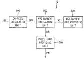
도 1 및 2를 참조하면, 평균 전류 추출 장치(10)는 온-픽셀 계산부(100), 최대 전류 정보 제공부(300), 평균 전류 계산부(500) 및 픽셀 정보 제공부(200)를 포함한다. 평균 전류 추출 방법에서는 온-픽셀 계산부(100)가 영상 정보(IMI)에 상응하는 감마 정보(GI)에 기초하여 디스플레이 패널(DP)에 포함되는 픽셀들 중 턴-온되는 픽셀들에 상응하는 온-픽셀 비율(OPR)을 계산한다(S100). 도 10 내지 12에서 후술하는 바와 같이, 영상 정보(IMI)에 상응하는 감마 정보(GI)에 기초하여 디스플레이 패널(DP)에 포함되는 픽셀들은 턴-온될 수 있다. 예를 들어, 영상 정보(IMI)에 상응하는 감마 정보(GI)에 기초하여 디스플레이 패널(DP)에 포함되는 픽셀들이 모두 화이트를 나타내는 경우, 온-픽셀 비율(OPR)은 1 또는 100%일 수 있다. 영상 정보(IMI)에 상응하는 감마 정보(GI)에 기초하여 디스플레이 패널(DP)에 포함되는 픽셀들의 1/2이 화이트를 나타내는 경우, 온-픽셀 비율(OPR)은 0.5 또는 50%일 수 있다. 영상 정보(IMI)에 상응하는 감마 정보(GI)에 기초하여 디스플레이 패널(DP)에 포함되는 픽셀들의 3/4이 화이트를 나타내는 경우, 온-픽셀 비율(OPR)은 0.75 또는 75%일 수 있다.1 and 2 , the average
최대 전류 정보 제공부(300)가 디밍 레벨(DL)에 상응하는 최대 전류 정보(MCI)를 제공한다(S110). 최대 전류 정보(MCI)는 디밍 레벨(DL)에 상응하는 최대 전류(MC) 값일 수 있다. 도 9에서 후술하는 바와 같이, 디스플레이 패널(DP)이 포함되는 디스플레이 장치(20)의 디밍 레벨(DL)에 따라 디스플레이 패널(DP)의 최대 전류 정보(MCI)는 변동할 수 있다. 디스플레이 패널(DP)이 포함되는 디스플레이 장치(20)의 디밍 레벨(DL)이 증가함에 따라 디스플레이 패널(DP)의 최대 전류 정보(MCI)에 상응하는 최대 전류(MC)는 증가할 수 있다. 예를 들어, 디스플레이 패널(DP)이 포함되는 디스플레이 장치(20)의 디밍 레벨(DL)이 1인 경우, 디스플레이 패널(DP)의 최대 전류 정보(MCI)에 상응하는 최대 전류(MC)는 10일 수 있고, 디스플레이 패널(DP)이 포함되는 디스플레이 장치(20)의 디밍 레벨(DL)이 3인 경우, 디스플레이 패널(DP)의 최대 전류 정보(MCI)에 상응하는 최대 전류(MC)는 100일 수 있다.The maximum current
평균 전류 계산부(500)가 온-픽셀 비율(OPR) 및 최대 전류 정보(MCI)에 기초하여 디스플레이 패널(DP)의 평균 전류(DAI)를 계산한다(S120). 디스플레이 패널(DP)의 평균 전류(DAI)는 온-픽셀 비율(OPR)과 최대 전류 정보(MCI)에 상응하는 최대 전류(MC)를 곱한 값일 수 있다. 예를 들어, 온-픽셀 비율(OPR)이 1이고, 디밍 레벨(DL)은 1일 일 수 있다. 디밍 레벨(DL)이 1인 경우, 최대 전류 정보(MCI)에 상응하는 최대 전류(MC)는 10일 수 있다. 이 경우, 디스플레이 패널(DP)의 평균 전류(DAI)는 온-픽셀 비율(OPR)과 최대 전류 정보(MCI)에 상응하는 최대 전류(MC)를 곱한 값에 해당하는 10일 수 있다. 또한, 온-픽셀 비율(OPR)이 0.5이고, 디밍 레벨(DL)은 1일 일 수 있다. 디밍 레벨(DL)이 1인 경우, 최대 전류 정보(MCI)에 상응하는 최대 전류(MC)는 10일 수 있다. 이 경우, 디스플레이 패널(DP)의 평균 전류(DAI)는 온-픽셀 비율(OPR)과 최대 전류 정보(MCI)에 상응하는 최대 전류(MC)를 곱한 값에 해당하는 5일 수 있다. 또한 온-픽셀 비율(OPR)이 0.5이고, 디밍 레벨(DL)은 3일 일 수 있다. 디밍 레벨(DL)이 3인 경우, 최대 전류 정보(MCI)에 상응하는 최대 전류(MC)는 100일 수 있다. 이 경우, 디스플레이 패널(DP)의 평균 전류(DAI)는 온-픽셀 비율(OPR)과 최대 전류 정보(MCI)에 상응하는 최대 전류(MC)를 곱한 값에 해당하는 50일 수 있다.The average
픽셀 정보 제공부(200)가 디스플레이 패널(DP)의 평균 전류(DAI)에 따라 결정되는 픽셀들 각각에 대한 픽셀 평균 전류 정보(PAI)를 제공한다(S130). 픽셀 평균 전류 정보(PAI)는 픽셀 평균 전류(PAC) 값일 수 있다. 도 5에서 후술하는 바와 같이, 디스플레이 패널(DP)의 평균 전류(DAI)에 따라 디스플레이 패널(DP)에 포함되는 픽셀들 각각에 대한 픽셀 평균 전류(PAC)가 변동될 수 있다. 디스플레이 패널(DP)의 평균 전류(DAI)가 결정되면, 디스플레이 패널(DP)에 포함되는 픽셀들 각각에 대한 픽셀 평균 전류(PAC)가 결정될 수 있다. 디스플레이 패널(DP)에 포함되는 픽셀들 각각에 대한 픽셀 평균 전류 정보(PAI)는 픽셀 평균 전류 룩-업 테이블(PACLT)에 저장될 수 있다.The pixel
본 발명의 실시예들에 따른 평균 전류 추출 방법은 디스플레이 패널(DP)의 평균 전류(DAI)에 기초하여 픽셀들 각각에 대한 픽셀 평균 전류 정보(PAI)를 제공함으로써 디스플레이 패널(DP)의 열화를 보상할 수 있다.The average current extraction method according to embodiments of the present invention prevents deterioration of the display panel DP by providing pixel average current information PAI for each pixel based on the average current DAI of the display panel DP. can be compensated
도 3 및 4는 픽셀 평균 전류에 따른 열화를 설명하기 위한 도면들이다.3 and 4 are diagrams for explaining deterioration according to an average pixel current.
도 3 및 4를 참조하면, 데이터 전압(VD)에 기초하여 트랜지스터(75)가 턴-온되는 경우, 유기 발광 다이오드(76)를 통해서 전류가 전달될 수 있다. 유기 발광 다이오드(76)를 통해서 전달되는 픽셀 평균 전류(PAC)에 따라 픽셀의 열화의 정도가 달라질 수 있다. 예를 들어, 유기 발광 다이오드(76)를 통해서 전달되는 픽셀 평균 전류(PAC)는 제1 픽셀 평균 전류(PAC1)일 수 있고, 유기 발광 다이오드(76)를 통해서 전달되는 픽셀 평균 전류(PAC)는 제2 픽셀 평균 전류(PAC2)일 수 있고, 유기 발광 다이오드(76)를 통해서 전달되는 픽셀 평균 전류(PAC)는 제3 픽셀 평균 전류(PAC3)일 수 있다. 제1 픽셀 평균 전류(PAC1)는 제2 픽셀 평균 전류(PAC2)보다 클 수 있다. 제2 픽셀 평균 전류(PAC2)는 제3 픽셀 평균 전류(PAC3)보다 클 수 있다. 유기 발광 다이오드(76)를 통해서 전달되는 픽셀 평균 전류(PAC)가 증가함에 따라 픽셀의 열화의 정도가 증가할 수 있다. 예를 들어 유기 발광 다이오드(76)를 통해서 전달되는 픽셀 평균 전류(PAC)가 제1 픽셀 평균 전류(PAC1)인 경우, 열화의 정도는 가장 높을 수 있다. 유기 발광 다이오드(76)를 통해서 전달되는 픽셀 평균 전류(PAC)가 제2 픽셀 평균 전류(PAC2)인 경우, 열화의 정도는 두 번째로 높을 수 있다. 유기 발광 다이오드(76)를 통해서 전달되는 픽셀 평균 전류(PAC)가 제3 픽셀 평균 전류(PAC3)인 경우, 열화의 정도는 가장 낮을 수 있다. 유기 발광 다이오드(76)를 통해서 전달되는 픽셀 평균 전류(PAC)에 따라 픽셀의 열화의 정도가 달라질 수 있다.3 and 4 , when the
도 5는 픽셀 평균 전류 룩-업 테이블을 설명하기 위한 도면이다.5 is a diagram for describing a pixel average current look-up table.
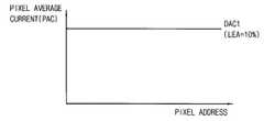
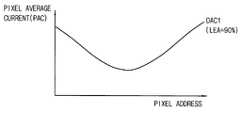
도 5를 참조하면, 디스플레이 패널(DP)의 평균 전류(DAI)에 따라 디스플레이 패널(DP)에 포함되는 픽셀들 각각에 대한 픽셀 평균 전류(PAC)가 변동될 수 있다. 디스플레이 패널(DP)의 평균 전류(DAI)가 결정되면, 디스플레이 패널(DP)에 포함되는 픽셀들 각각에 대한 픽셀 평균 전류(PAC)가 결정될 수 있다. 디스플레이 패널(DP)에 포함되는 픽셀들 각각에 대한 픽셀 평균 전류 정보(PAI)는 픽셀 평균 전류 룩-업 테이블(PACLT)에 저장될 수 있다. 예를 들어, 디스플레이 패널(DP)의 평균 전류(DAI)는 제1 평균 전류(DAC1)일 수 있다. 디스플레이 패널(DP)의 평균 전류(DAI)는 제1 평균 전류(DAC1)인 경우, 픽셀 어드레스가 증가함에 따라 픽셀 평균 전류(PAC)는 감소한 후 증가할 수 있다. 픽셀 어드레스는 하나의 스캔라인과 연결되는 픽셀들의 어드레스들일 수 있다. 또한, 디스플레이 패널(DP)의 평균 전류(DAI)는 제2 평균 전류(DAC2)일 수 있다. 디스플레이 패널(DP)의 평균 전류(DAI)는 제2 평균 전류(DAC2)인 경우, 픽셀 어드레스가 증가함에 따라 픽셀 평균 전류(PAC)는 감소한 후 증가할 수 있다. 이 경우, 제2 평균 전류(DAC2)의 경우에서 픽셀 평균 전류(PAC)의 감소 폭은 제1 평균 전류(DAC1)의 경우에서의 픽셀 평균 전류(PAC)의 감소 폭보다 작을 수 있다. 또한, 디스플레이 패널(DP)의 평균 전류(DAI)는 제3 평균 전류(DAC3)일 수 있다. 디스플레이 패널(DP)의 평균 전류(DAI)는 제3 평균 전류(DAC3)인 경우, 픽셀 어드레스가 증가함에 따라 픽셀 평균 전류(PAC)는 일정할 수 있다. 디스플레이 패널(DP)의 평균 전류(DAI)에 따른 픽셀들 각각에 대한 픽셀 평균 전류 정보(PAI)는 픽셀 평균 전류 룩-업 테이블(PACLT)에 저장될 수 있다. 예를 들어, 픽셀 정보 제공부(200)는 픽셀들 각각에 대한 픽셀 평균 전류 정보(PAI)를 저장하는 픽셀 평균 전류 룩-업 테이블(PACLT)을 포함할 수 있다.Referring to FIG. 5 , the pixel average current PAC for each of the pixels included in the display panel DP may vary according to the average current DAI of the display panel DP. When the average current DAI of the display panel DP is determined, the pixel average current PAC for each of the pixels included in the display panel DP may be determined. The pixel average current information PAI for each of the pixels included in the display panel DP may be stored in the pixel average current look-up table PACLT. For example, the average current DAI of the display panel DP may be the first average current DAC1 . When the average current DAI of the display panel DP is the first average current DAC1 , the pixel average current PAC decreases and then increases as the pixel address increases. The pixel address may be addresses of pixels connected to one scan line. Also, the average current DAI of the display panel DP may be the second average current DAC2 . When the average current DAI of the display panel DP is the second average current DAC2 , the pixel average current PAC decreases and then increases as the pixel address increases. In this case, the decrease width of the pixel average current PAC in the case of the second average current DAC2 may be smaller than the decrease width of the pixel average current PAC in the case of the first average current DAC1 . Also, the average current DAI of the display panel DP may be the third average current DAC3 . When the average current DAI of the display panel DP is the third average current DAC3, the pixel average current PAC may be constant as the pixel address increases. The pixel average current information PAI for each of the pixels according to the average current DAI of the display panel DP may be stored in the pixel average current look-up table PACLT. For example, the pixel
본 발명의 실시예들에 따른 평균 전류 추출 방법은 디스플레이 패널(DP)의 평균 전류(DAI)에 기초하여 픽셀들 각각에 대한 픽셀 평균 전류 정보(PAI)를 제공함으로써 디스플레이 패널(DP)의 열화를 보상할 수 있다.The average current extraction method according to embodiments of the present invention prevents deterioration of the display panel DP by providing pixel average current information PAI for each pixel based on the average current DAI of the display panel DP. can be compensated
도 6은 픽셀 평균 전류 룩-업 테이블에 포함되는 픽셀들 각각에 대한 픽셀 평균 전류 정보를 갱신하는 일 예를 설명하기 위한 도면이다.6 is a diagram for explaining an example of updating pixel average current information for each of the pixels included in the pixel average current look-up table.
도 6을 참조하면, 픽셀 평균 전류 룩-업 테이블(PACLT)에 포함되는 픽셀들 각각에 대한 픽셀 평균 전류 정보(PAI)는 미리 정해진 시간 간격(PDT)마다 갱신될 수 있다. 예를 들어, 제1 시간(T1)에 평균 전류 추출 장치(10)는 제1 픽셀 전류(PC1)에 기초하여 픽셀 평균 전류 룩-업 테이블(PACLT)에 포함되는 픽셀에 대한 픽셀 평균 전류 정보(PAI)를 갱신할 수 있다. 제1 픽셀 전류(PC1)는 제1 시간(T1)에 유기 발광 다이오드(76)에 전달되는 전류일 수 있다. 제2 시간(T2)에 평균 전류 추출 장치(10)는 제2 픽셀 전류(PC2)에 기초하여 픽셀 평균 전류 룩-업 테이블(PACLT)에 포함되는 픽셀에 대한 픽셀 평균 전류 정보(PAI)를 갱신할 수 있다. 제2 픽셀 전류(PC2)는 제2 시간(T2)에 유기 발광 다이오드(76)에 전달되는 전류일 수 있다. 제3 시간(T3)에 평균 전류 추출 장치(10)는 제3 픽셀 전류(PC3)에 기초하여 픽셀 평균 전류 룩-업 테이블(PACLT)에 포함되는 픽셀에 대한 픽셀 평균 전류 정보(PAI)를 갱신할 수 있다. 제3 픽셀 전류(PC3)는 제3 시간(T3)에 유기 발광 다이오드(76)에 전달되는 전류일 수 있다. 제1 시간(T1)과 제2 시간(T2) 사이의 간격은 미리 정해진 시간 간격(PDT)일 수 있다. 제2 시간(T2)과 제3 시간(T3) 사이의 간격은 미리 정해진 시간 간격(PDT)일 수 있다.Referring to FIG. 6 , the pixel average current information PAI for each of the pixels included in the pixel average current look-up table PACLT may be updated at predetermined time intervals PDT. For example, at a first time T1 , the average
본 발명의 실시예들에 따른 평균 전류 추출 방법은 디스플레이 패널(DP)의 평균 전류(DAI)에 기초하여 픽셀들 각각에 대한 픽셀 평균 전류 정보(PAI)를 제공함으로써 디스플레이 패널(DP)의 열화를 보상할 수 있다.The average current extraction method according to embodiments of the present invention prevents deterioration of the display panel DP by providing pixel average current information PAI for each pixel based on the average current DAI of the display panel DP. can be compensated
도 7 및 8은 픽셀 평균 전류 룩-업 테이블에 포함되는 픽셀들 각각에 대한 픽셀 평균 전류 정보를 갱신하는 다른 예를 설명하기 위한 도면이다.7 and 8 are diagrams for explaining another example of updating pixel average current information for each of the pixels included in the pixel average current look-up table.
도 7 및 8을 참조하면, 미리 정해진 시간 간격(PDT)은 미리 정해진 프레임 간격일 수 있다. 예시적인 실시예에 있어서, 픽셀 평균 전류 룩-업 테이블(PACLT)을 갱신하고, 미리 정해진 프레임 간격이 경과한 후, 픽셀의 전류(PC)가 0이면, 픽셀에 대한 픽셀 평균 전류 정보(PAI)는 갱신되지 않을 수 있다. 예를 들어, 미리 정해진 프레임 간격은 하나의 프레임 간격일 수 있다. 제1 프레임(F1)에서 제1 픽셀(PIXEL1)에 포함되는 유기 발광 다이오드(76)에 전달되는 제1 픽셀 전류(PC1)는 5일 수 있다. 제1 프레임(F1)에서 제1 픽셀(PIXEL1)에 포함되는 유기 발광 다이오드(76)에 전달되는 제1 픽셀 전류(PC1)는 5인 경우, 제1 픽셀 평균 전류(PAC1)는 5일 수 있다. 제1 픽셀 평균 전류(PAC1)는 5인 경우, 픽셀 평균 전류 룩-업 테이블(PACLT)에서 제1 픽셀 평균 전류(PAC1)에 상응하는 픽셀 평균 전류 정보(PAI)는 5로 갱신될 수 있다. 또한 제2 프레임(F2)에서 제1 픽셀(PIXEL1)에 포함되는 유기 발광 다이오드(76)에 전달되는 제2 픽셀 전류(PC2)는 0일 수 있다. 제2 프레임(F2)에서 제1 픽셀(PIXEL1)에 포함되는 유기 발광 다이오드(76)에 전달되는 제2 픽셀 전류(PC2)는 0인 경우, 제2 픽셀 평균 전류(PAC2)는 5일 수 있다. 이와 같이, 픽셀 평균 전류 룩-업 테이블(PACLT)을 갱신하고, 미리 정해진 프레임 간격이 경과한 후, 픽셀의 전류가 0이면, 픽셀에 대한 픽셀 평균 전류 정보(PAI)는 갱신되지 않을 수 있다.7 and 8 , the predetermined time interval PDT may be a predetermined frame interval. In an exemplary embodiment, after updating the pixel average current look-up table (PACLT), and after a predetermined frame interval elapses, if the pixel current (PC) is zero, the pixel average current information (PAI) for the pixel may not be updated. For example, the predetermined frame interval may be one frame interval. In the first frame F1 , the first pixel current PC1 transferred to the organic
예시적인 실시예에 있어서, 픽셀 평균 전류 룩-업 테이블(PACLT)을 갱신하고, 미리 정해진 프레임 간격이 경과한 후, 픽셀의 전류(PC)가 0이 아니면, 픽셀에 대한 픽셀 평균 전류 정보(PAI)는 갱신될 수 있다. 예를 들어, 제3 프레임(F3)에서 제1 픽셀(PIXEL1)에 포함되는 유기 발광 다이오드(76)에 전달되는 제3 픽셀 전류(PC3)는 4일 수 있다. 제3 프레임(F3)에서 제1 픽셀(PIXEL1)에 포함되는 유기 발광 다이오드(76)에 전달되는 제3 픽셀 전류(PC3)는 4인 경우, 제3 픽셀 평균 전류(PAC3)는 (5+4)/3=3일 수 있다. 제3 픽셀 평균 전류(PAC3)는 3인 경우, 픽셀 평균 전류 룩-업 테이블(PACLT)에서 제3 픽셀 평균 전류(PAC3)에 상응하는 픽셀 평균 전류 정보(PAI)는 3으로 갱신될 수 있다. 결과적으로, 제1 프레임(F1)에서는 제1 픽셀(PIXEL1)에 대한 픽셀 평균 전류 정보(PAI)는 5로 갱신될 수 있고, 제2 프레임(F2)에서는 제1 픽셀(PIXEL1)에 대한 픽셀 평균 전류 정보(PAI)는 갱신되지 않을 수 있다. 제3 프레임(F3)에서는 제1 픽셀(PIXEL1)에 대한 픽셀 평균 전류 정보(PAI)는 3으로 갱신될 수 있다.In an exemplary embodiment, if the pixel average current look-up table (PACLT) is updated, and after a predetermined frame interval has elapsed, the pixel current (PC) is non-zero, the pixel average current information (PAI) for the pixel ) can be updated. For example, the third pixel current PC3 transferred to the organic
본 발명의 실시예들에 따른 평균 전류 추출 방법은 디스플레이 패널(DP)의 평균 전류(DAI)에 기초하여 픽셀들 각각에 대한 픽셀 평균 전류 정보(PAI)를 제공함으로써 디스플레이 패널(DP)의 열화를 보상할 수 있다.The average current extraction method according to embodiments of the present invention prevents deterioration of the display panel DP by providing pixel average current information PAI for each pixel based on the average current DAI of the display panel DP. can be compensated
도 9는 최대 전류 룩-업 테이블을 설명하기 위한 도면이고, 도 10은 최대 전류 정보에 상응하는 최대 전류 값을 설명하기 위한 도면이다.9 is a diagram for explaining a maximum current look-up table, and FIG. 10 is a diagram for explaining a maximum current value corresponding to maximum current information.
도 9를 참조하면, 최대 전류 정보 제공부(300)는 디밍 레벨(DL)에 상응하는 최대 전류 정보(MCI)를 저장하는 최대 전류 룩-업 테이블(MCLT)을 포함할 수 있다. 디밍 레벨(DL)에 상응하는 최대 전류 정보(MCI)는 디스플레이 패널(DP)이 동작하기 전에 최대 전류 룩-업 테이블(MCLT)에 저장될 수 있다. 디밍 레벨(DL)이 증가함에 따라 최대 전류 정보(MCI)에 상응하는 최대 전류(MC)값은 증가할 수 있다. 예를 들어, 평균 전류 추출 장치(10)를 포함하는 디스플레이 장치(20)의 디밍 레벨(DL)이 0인 경우, 최대 전류 정보(MCI)에 상응하는 최대 전류(MC)값은 0일 수 있다. 디스플레이 장치(20)의 디밍 레벨(DL)이 1인 경우, 최대 전류 정보(MCI)에 상응하는 최대 전류(MC)값은 10일 수 있다. 디스플레이 장치(20)의 디밍 레벨(DL)이 2인 경우, 최대 전류 정보(MCI)에 상응하는 최대 전류(MC)값은 50일 수 있다. 디스플레이 장치(20)의 디밍 레벨(DL)이 3인 경우, 최대 전류 정보(MCI)에 상응하는 최대 전류(MC)값은 100일 수 있다. 따라서, 디밍 레벨(DL)이 증가함에 따라 최대 전류 정보(MCI)에 상응하는 최대 전류(MC)값은 증가할 수 있다. 최대 전류 정보(MCI)에 상응하는 최대 전류(MC)값은 디스플레이 패널(DP)의 평균 전류(DAI)를 계산하기 위하여 이용될 수 있다.Referring to FIG. 9 , the maximum current
도 9 및 10을 참조하면, 온-픽셀 비율(OPR)이 1일 수 있다. 디스플레이 장치(20)의 디밍 레벨(DL)이 1인 경우, 최대 전류 정보(MCI)에 상응하는 최대 전류(MC)값은 10일 수 있다. 이 경우, 디스플레이 패널(DP)의 평균 전류(DAI)는 10일 수 있다. 또한, 디스플레이 장치(20)의 디밍 레벨(DL)이 2인 경우, 최대 전류 정보(MCI)에 상응하는 최대 전류(MC)값은 50일 수 있다. 이 경우, 디스플레이 패널(DP)의 평균 전류(DAI)는 50일 수 있다. 또한, 디스플레이 장치(20)의 디밍 레벨(DL)이 3인 경우, 최대 전류 정보(MCI)에 상응하는 최대 전류(MC)값은 100일 수 있다. 이 경우, 디스플레이 패널(DP)의 평균 전류(DAI)는 100일 수 있다.9 and 10 , the on-pixel ratio (OPR) may be 1. When the dimming level DL of the
도 11 및 12는 온-픽셀 비율에 따른 디스플레이 패널의 평균 전류를 설명하기 위한 도면들이다.11 and 12 are diagrams for explaining an average current of a display panel according to an on-pixel ratio.
도 9, 11 및 12를 참조하면, 디스플레이 패널(DP)의 평균 전류(DAI)는 최대 전류 정보(MCI)에 상응하는 최대 전류(MC) 값보다 같거나 작을 수 있다. 예를 들어, 온-픽셀 비율(OPR)이 1 인 경우, 디스플레이 패널(DP)의 평균 전류(DAI)는 최대 전류 정보(MCI)에 상응하는 최대 전류(MC) 값과 같을 수 있다. 온-픽셀 비율(OPR)이 1보다 작은 경우, 디스플레이 패널(DP)의 평균 전류(DAI)는 최대 전류 정보(MCI)에 상응하는 최대 전류(MC) 값보다 작을 수 있다.9, 11 and 12 , the average current DAI of the display panel DP may be equal to or smaller than the maximum current MC value corresponding to the maximum current information MCI. For example, when the on-pixel ratio OPR is 1, the average current DAI of the display panel DP may be equal to the maximum current MC value corresponding to the maximum current information MCI. When the on-pixel ratio OPR is less than 1, the average current DAI of the display panel DP may be less than the maximum current MC value corresponding to the maximum current information MCI.
예시적인 실시예에 있어서, 온-픽셀 비율(OPR)이 증가함에 따라 디스플레이 패널(DP)의 평균 전류(DAI)는 증가할 수 있다. 예를 들어, 디스플레이 장치(20)의 디밍 레벨(DL)이 3인 경우, 최대 전류 정보(MCI)에 상응하는 최대 전류(MC)값은 100일 수 있다. 디스플레이 장치(20)의 디밍 레벨(DL)은 3이고, 온-픽셀 비율(OPR)은 0.5인 경우, 디스플레이 패널(DP)의 평균 전류(DAI)는 50일 수 있다. 또한, 디스플레이 장치(20)의 디밍 레벨(DL)은 3이고, 온-픽셀 비율(OPR)은 0.75인 경우, 디스플레이 패널(DP)의 평균 전류(DAI)는 75일 수 있다. 따라서, 온-픽셀 비율(OPR)이 증가함에 따라 디스플레이 패널(DP)의 평균 전류(DAI)는 증가할 수 있다.In an exemplary embodiment, as the on-pixel ratio OPR increases, the average current DAI of the display panel DP may increase. For example, when the dimming level DL of the
예시적인 실시예에 있어서, 최대 전류 정보(MCI)에 상응하는 최대 전류(MC) 값이 증가함에 따라 디스플레이 패널(DP)의 평균 전류(DAI)는 증가할 수 있다. 예를 들어, 온-픽셀 비율(OPR)이 0.5일 수 있다. 디스플레이 장치(20)의 디밍 레벨(DL)이 1인 경우, 최대 전류 정보(MCI)에 상응하는 최대 전류(MC)값은 10일 수 있다. 이 경우, 디스플레이 패널(DP)의 평균 전류(DAI)는 5일 수 있다. 또한, 디스플레이 장치(20)의 디밍 레벨(DL)이 2인 경우, 최대 전류 정보(MCI)에 상응하는 최대 전류(MC)값은 50일 수 있다. 이 경우, 디스플레이 패널(DP)의 평균 전류(DAI)는 25일 수 있다. 또한, 디스플레이 장치(20)의 디밍 레벨(DL)이 3인 경우, 최대 전류 정보(MCI)에 상응하는 최대 전류(MC)값은 100일 수 있다. 이 경우, 디스플레이 패널(DP)의 평균 전류(DAI)는 50일 수 있다. 예를 들어, 디스플레이 패널(DP)의 평균 전류(DAI)는 온-픽셀 비율(OPR) 및 최대 전류 정보에 상응하는 최대 전류(MC)값을 곱한 값일 수 있다.In an exemplary embodiment, as the maximum current MC value corresponding to the maximum current information MCI increases, the average current DAI of the display panel DP may increase. For example, the on-pixel ratio (OPR) may be 0.5. When the dimming level DL of the
본 발명의 실시예들에 따른 평균 전류 추출 방법은 디스플레이 패널(DP)의 평균 전류(DAI)에 기초하여 픽셀들 각각에 대한 픽셀 평균 전류 정보(PAI)를 제공함으로써 디스플레이 패널(DP)의 열화를 보상할 수 있다.The average current extraction method according to embodiments of the present invention prevents deterioration of the display panel DP by providing pixel average current information PAI for each pixel based on the average current DAI of the display panel DP. can be compensated
도 13은 본 발명의 일 실시예에 따른 평균 전류 추출 장치를 나타내는 블록도이고, 도 14 내지 16은 발광 면적에 따른 픽셀 평균 전류 룩-업 테이블의 예들을 설명하기 위한 도면들이다.13 is a block diagram illustrating an average current extraction apparatus according to an embodiment of the present invention, and FIGS. 14 to 16 are diagrams for explaining examples of pixel average current look-up tables according to emission areas.
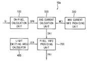
도 13을 참조하면, 평균 전류 추출 장치(10a)는 온-픽셀 계산부(100), 최대 전류 정보 제공부(300), 평균 전류 계산부(500) 및 픽셀 정보 제공부(200)를 포함한다. 평균 전류 추출 방법에서는 온-픽셀 계산부(100)가 영상 정보(IMI)에 상응하는 감마 정보(GI)에 기초하여 디스플레이 패널(DP)에 포함되는 픽셀들 중 턴-온되는 픽셀들에 상응하는 온-픽셀 비율(OPR)을 계산한다. 최대 전류 정보 제공부(300)가 디밍 레벨(DL)에 상응하는 최대 전류 정보(MCI)를 제공한다. 평균 전류 계산부(500)가 온-픽셀 비율(OPR) 및 최대 전류 정보(MCI)에 기초하여 디스플레이 패널(DP)의 평균 전류(DAI)를 계산한다. 픽셀 정보 제공부(200)가 디스플레이 패널(DP)의 평균 전류(DAI)에 따라 결정되는 픽셀들 각각에 대한 픽셀 평균 전류 정보(PAI)를 제공한다.Referring to FIG. 13 , the average
예시적인 실시예에 있어서, 디스플레이 패널(DP)을 포함하는 디스플레이 장치(20)는 디스플레이 패널(DP)의 발광 면적(LEA)을 계산하는 발광 면적 계산기(400)를 더 포함할 수 있다.In an exemplary embodiment, the
도 14 내지 16을 참조하면, 픽셀 정보 제공부(200)는 디스플레이 패널(DP)의 발광 면적(LEA)에 기초하여 픽셀 평균 전류 룩-업 테이블(PACLT)을 변경할 수 있다. 예를 들어, 디스플레이 패널(DP)의 평균 전류(DAI)는 제1 평균 전류(DAC1)일 수 있다. 이 경우, 발광 면적(LEA)에 따른 픽셀 평균 전류 룩-업 테이블(PACLT)은 도 5의 제1 평균 전류(DAC1)에 따른 곡선에 기초하여 생성될 수 있다. 발광 면적(LEA)이 90%인 경우, 픽셀 평균 전류 룩-업 테이블(PACLT)은 도 5의 제1 평균 전류(DAC1)에 따른 곡선과 유사할 수 있다. 발광 면적(LEA)이 감소함에 따라 픽셀 평균 전류 룩-업 테이블(PACLT)에 저장되는 픽셀 평균 전류 정보(PAI)에 상응하는 픽셀 평균 전류(PAC)값의 변동 폭은 감소할 수 있다. 예를 들어, 디스플레이 패널(DP)의 발광 면적(LEA)이 감소함에 따라 픽셀들에 대한 픽셀 평균 전류 정보(PAI)들의 편차는 감소할 수 있다. 픽셀 평균 전류 룩-업 테이블(PACLT)은 발광 면적(LEA)에 따라 별도로 저장될 수 있다.14 to 16 , the pixel
본 발명의 실시예들에 따른 평균 전류 추출 방법은 디스플레이 패널(DP)의 평균 전류(DAI)에 기초하여 픽셀들 각각에 대한 픽셀 평균 전류 정보(PAI)를 제공함으로써 디스플레이 패널(DP)의 열화를 보상할 수 있다.The average current extraction method according to embodiments of the present invention prevents deterioration of the display panel DP by providing pixel average current information PAI for each pixel based on the average current DAI of the display panel DP. can be compensated
도 17은 본 발명의 실시예들에 따른 영상 정보 보상 방법을 나타내는 순서도이고, 도 18은 본 발명의 실시예들에 따른 영상 정보 보상 장치를 나타내는 블록도이다.17 is a flowchart illustrating a method for compensating image information according to embodiments of the present invention, and FIG. 18 is a block diagram illustrating an apparatus for compensating image information according to embodiments of the present invention.
도 17 및 18을 참조하면, 영상 정보 보상 장치(15)는 온-픽셀 계산부(100), 최대 전류 정보 제공부(300), 평균 전류 계산부(500), 픽셀 정보 제공부(200) 및 보상 계수 생성기(210)를 포함한다. 영상 정보 보상 방법에서는 온-픽셀 계산부(100)가 영상 정보(IMI)에 상응하는 감마 정보(GI)에 기초하여 디스플레이 패널(DP)에 포함되는 픽셀들 중 턴-온되는 픽셀들에 상응하는 온-픽셀 비율(OPR)을 계산한다(S200). 영상 정보(IMI)에 상응하는 감마 정보(GI)에 기초하여 디스플레이 패널(DP)에 포함되는 픽셀들은 턴-온될 수 있다. 예를 들어, 영상 정보(IMI)에 상응하는 감마 정보(GI)에 기초하여 디스플레이 패널(DP)에 포함되는 픽셀들이 모두 화이트를 나타내는 경우, 온-픽셀 비율(OPR)은 1 또는 100%일 수 있다. 영상 정보(IMI)에 상응하는 감마 정보(GI)에 기초하여 디스플레이 패널(DP)에 포함되는 픽셀들의 1/2이 화이트를 나타내는 경우, 온-픽셀 비율(OPR)은 0.5 또는 50%일 수 있다. 영상 정보(IMI)에 상응하는 감마 정보(GI)에 기초하여 디스플레이 패널(DP)에 포함되는 픽셀들의 3/4이 화이트를 나타내는 경우, 온-픽셀 비율(OPR)은 0.75 또는 75%일 수 있다.17 and 18 , the image
최대 전류 정보 제공부(300)가 디밍 레벨(DL)에 상응하는 최대 전류 정보(MCI)를 제공한다(S210). 최대 전류 정보(MCI)는 디밍 레벨(DL)에 상응하는 최대 전류(MC) 값일 수 있다. 디스플레이 패널(DP)이 포함되는 디스플레이 장치(20)의 디밍 레벨(DL)에 따라 디스플레이 패널(DP)의 최대 전류 정보(MCI)는 변동할 수 있다. 디스플레이 패널(DP)이 포함되는 디스플레이 장치(20)의 디밍 레벨(DL)이 증가함에 따라 디스플레이 패널(DP)의 최대 전류 정보(MCI)에 상응하는 최대 전류(MC)는 증가할 수 있다. 예를 들어, 디스플레이 패널(DP)이 포함되는 디스플레이 장치(20)의 디밍 레벨(DL)이 1인 경우, 디스플레이 패널(DP)의 최대 전류 정보(MCI)에 상응하는 최대 전류(MC)는 10일 수 있고, 디스플레이 패널(DP)이 포함되는 디스플레이 장치(20)의 디밍 레벨(DL)이 3인 경우, 디스플레이 패널(DP)의 최대 전류 정보(MCI)에 상응하는 최대 전류(MC)는 100일 수 있다.The maximum current
평균 전류 계산부(500)가 온-픽셀 비율(OPR) 및 최대 전류 정보(MCI)에 기초하여 디스플레이 패널(DP)의 평균 전류(DAI)를 계산한다(S220). 디스플레이 패널(DP)의 평균 전류(DAI)는 온-픽셀 비율(OPR)과 최대 전류 정보(MCI)에 상응하는 최대 전류(MC)를 곱한 값일 수 있다. 예를 들어, 온-픽셀 비율(OPR)이 1이고, 디밍 레벨(DL)은 1일 일 수 있다. 디밍 레벨(DL)이 1인 경우, 최대 전류 정보(MCI)에 상응하는 최대 전류(MC)는 10일 수 있다. 이 경우, 디스플레이 패널(DP)의 평균 전류(DAI)는 온-픽셀 비율(OPR)과 최대 전류 정보(MCI)에 상응하는 최대 전류(MC)를 곱한 값에 해당하는 10일 수 있다. 또한, 온-픽셀 비율(OPR)이 0.5이고, 디밍 레벨(DL)은 1일 일 수 있다. 디밍 레벨(DL)이 1인 경우, 최대 전류 정보(MCI)에 상응하는 최대 전류(MC)는 10일 수 있다. 이 경우, 디스플레이 패널(DP)의 평균 전류(DAI)는 온-픽셀 비율(OPR)과 최대 전류 정보(MCI)에 상응하는 최대 전류(MC)를 곱한 값에 해당하는 5일 수 있다. 또한 온-픽셀 비율(OPR)이 0.5이고, 디밍 레벨(DL)은 3일 일 수 있다. 디밍 레벨(DL)이 3인 경우, 최대 전류 정보(MCI)에 상응하는 최대 전류(MC)는 100일 수 있다. 이 경우, 디스플레이 패널(DP)의 평균 전류(DAI)는 온-픽셀 비율(OPR)과 최대 전류 정보(MCI)에 상응하는 최대 전류(MC)를 곱한 값에 해당하는 50일 수 있다.The average
픽셀 정보 제공부(200)가 디스플레이 패널(DP)의 평균 전류(DAI)에 따라 결정되는 픽셀들 각각에 대한 픽셀 평균 전류 정보(PAI)를 제공한다(S230) 픽셀 평균 전류 정보(PAI)는 픽셀 평균 전류(PAC) 값일 수 있다. 디스플레이 패널(DP)의 평균 전류(DAI)에 따라 디스플레이 패널(DP)에 포함되는 픽셀들 각각에 대한 픽셀 평균 전류(PAC)가 변동될 수 있다. 디스플레이 패널(DP)의 평균 전류(DAI)가 결정되면, 디스플레이 패널(DP)에 포함되는 픽셀들 각각에 대한 픽셀 평균 전류(PAC)가 결정될 수 있다. 디스플레이 패널(DP)에 포함되는 픽셀들 각각에 대한 픽셀 평균 전류 정보(PAI)는 픽셀 평균 전류 룩-업 테이블(PACLT)에 저장될 수 있다.The pixel
픽셀들 각각에 대한 픽셀 평균 전류 정보(PAI)에 기초하여 영상 정보(IMI)에 상응하는 감마 정보(GI)를 보상한다(S240). 예시적인 실시예에 있어서, 디스플레이 패널(DP)을 포함하는 디스플레이 장치(20)는 픽셀들 각각에 대한 픽셀 평균 전류 정보(PAI)에 기초하여 감마 정보(GI)를 보상하는 보상 계수(CC)를 생성하는 보상 계수 생성기(210)를 더 포함할 수 있다. 예를 들어, 보상 계수 생성기(210)로부터 생성되는 보상 계수(CC)를 이용하여 영상 정보(IMI)에 상응하는 감마 정보(GI)를 보상할 수 있다.The gamma information GI corresponding to the image information IMI is compensated based on the pixel average current information PAI for each pixel ( S240 ). In an exemplary embodiment, the
예시적인 실시예에 있어서, 픽셀 정보 제공부(200)는 픽셀들 각각에 대한 픽셀 평균 전류 정보(PAI)를 저장하는 픽셀 평균 전류 룩-업 테이블(PACLT)을 포함하고, 픽셀 평균 전류 룩-업 테이블(PACLT)에 포함되는 픽셀들 각각에 대한 픽셀 평균 전류 정보(PAI)는 미리 정해진 시간 간격(PDT)마다 갱신될 수 있다. 디스플레이 패널(DP)의 평균 전류(DAI)에 따라 디스플레이 패널(DP)에 포함되는 픽셀들 각각에 대한 픽셀 평균 전류(PAC)가 변동될 수 있다. 디스플레이 패널(DP)의 평균 전류(DAI)가 결정되면, 디스플레이 패널(DP)에 포함되는 픽셀들 각각에 대한 픽셀 평균 전류(PAC)가 결정될 수 있다. 디스플레이 패널(DP)에 포함되는 픽셀들 각각에 대한 픽셀 평균 전류 정보(PAI)는 픽셀 평균 전류 룩-업 테이블(PACLT)에 저장될 수 있다. 예를 들어, 제1 시간(T1)에 평균 전류 추출 장치(10)는 제1 픽셀 전류(PC1)에 기초하여 픽셀 평균 전류 룩-업 테이블(PACLT)에 포함되는 픽셀에 대한 픽셀 평균 전류 정보(PAI)를 갱신할 수 있다. 제1 픽셀 전류(PC1)는 제1 시간(T1)에 유기 발광 다이오드(76)에 전달되는 전류일 수 있다. 제2 시간(T2)에 평균 전류 추출 장치(10)는 제2 픽셀 전류(PC2)에 기초하여 픽셀 평균 전류 룩-업 테이블(PACLT)에 포함되는 픽셀에 대한 픽셀 평균 전류 정보(PAI)를 갱신할 수 있다. 제2 픽셀 전류(PC2)는 제2 시간(T2)에 유기 발광 다이오드(76)에 전달되는 전류일 수 있다. 제3 시간(T3)에 평균 전류 추출 장치(10)는 제3 픽셀 전류(PC3)에 기초하여 픽셀 평균 전류 룩-업 테이블(PACLT)에 포함되는 픽셀에 대한 픽셀 평균 전류 정보(PAI)를 갱신할 수 있다. 제3 픽셀 전류(PC3)는 제3 시간(T3)에 유기 발광 다이오드(76)에 전달되는 전류일 수 있다. 제1 시간(T1)과 제2 시간(T2) 사이의 간격은 미리 정해진 시간 간격(PDT)일 수 있다. 제2 시간(T2)과 제3 시간(T3) 사이의 간격은 미리 정해진 시간 간격(PDT)일 수 있다.In an exemplary embodiment, the pixel
예시적인 실시예에 있어서, 최대 전류 정보 제공부(300)는 디밍 레벨(DL)에 상응하는 최대 전류 정보(MCI)를 저장하는 최대 전류 룩-업 테이블(MCLT)을 포함하고, 디밍 레벨(DL)이 증가함에 따라 최대 전류 정보(MCI)에 상응하는 최대 전류(MC)값은 증가할 수 있다. 디밍 레벨(DL)에 상응하는 최대 전류 정보(MCI)는 디스플레이 패널(DP)이 동작하기 전에 최대 전류 룩-업 테이블(MCLT)에 저장될 수 있다. 예를 들어, 평균 전류 추출 장치(10)를 포함하는 디스플레이 장치(20)의 디밍 레벨(DL)이 0인 경우, 최대 전류 정보(MCI)에 상응하는 최대 전류(MC)값은 0일 수 있다. 디스플레이 장치(20)의 디밍 레벨(DL)이 1인 경우, 최대 전류 정보(MCI)에 상응하는 최대 전류(MC)값은 10일 수 있다. 디스플레이 장치(20)의 디밍 레벨(DL)이 2인 경우, 최대 전류 정보(MCI)에 상응하는 최대 전류(MC)값은 50일 수 있다. 디스플레이 장치(20)의 디밍 레벨(DL)이 3인 경우, 최대 전류 정보(MCI)에 상응하는 최대 전류(MC)값은 100일 수 있다. 따라서, 디밍 레벨(DL)이 증가함에 따라 최대 전류 정보(MCI)에 상응하는 최대 전류(MC)값은 증가할 수 있다. 최대 전류 정보(MCI)에 상응하는 최대 전류(MC)값은 디스플레이 패널(DP)의 평균 전류(DAI)를 계산하기 위하여 이용될 수 있다.In an exemplary embodiment, the maximum current
본 발명의 실시예들에 따른 평균 전류 추출 방법은 디스플레이 패널(DP)의 평균 전류(DAI)에 기초하여 픽셀들 각각에 대한 픽셀 평균 전류 정보(PAI)를 제공함으로써 디스플레이 패널(DP)의 열화를 보상할 수 있다.The average current extraction method according to embodiments of the present invention prevents deterioration of the display panel DP by providing pixel average current information PAI for each pixel based on the average current DAI of the display panel DP. can be compensated
도 19는 본 발명의 일 실시예에 따른 디스플레이 장치를 나타내는 도면이다.19 is a diagram illustrating a display device according to an embodiment of the present invention.
도 19를 참조하면, 디스플레이 장치(20)는 감마부(230), 보상 계수 생성기(210), 보상부(250) 및 디스플레이 패널(270)을 포함할 수 있다. 감마부(230)는 영상 정보(IMI)에 상응하는 감마 정보(GI)를 제공할 수 있다. 보상 계수 생성기(210)는 픽셀 평균 전류 정보(PAI)에 기초하여 감마 정보(GI)를 보상하는 보상 계수(CC)를 생성할 수 있다. 보상부(250)는 영상 정보(IMI)에 상응하는 감마 정보(GI) 및 보상 계수(CC)에 기초하여 보상 감마 정보(CGI)를 제공할 수 있다. 디스플레이 패널(DP)은 보상 감마 정보(CGI)에 기초하여 영상을 디스플레이할 수 있다.Referring to FIG. 19 , the
도 20은 본 발명의 실시예들에 따른 디스플레이 장치를 컴퓨팅 시스템에 응용한 예를 나타내는 블록도이다.20 is a block diagram illustrating an example of applying a display device according to embodiments of the present invention to a computing system.
도 20을 참조하면, 컴퓨팅 시스템(700)는 프로세서(710), 메모리 장치(720), 저장 장치(730), 입출력 장치(740), 파워 서플라이(750) 및 디스플레이 장치(760)를 포함할 수 있다. 컴퓨팅 시스템(700)는 비디오 카드, 사운드 카드, 메모리 카드, USB 장치 등과 통신하거나, 또는 다른 시스템들과 통신할 수 있는 여러 포트(port)들을 더 포함할 수 있다.Referring to FIG. 20 , the
프로세서(710)는 특정 계산들 또는 태스크(task)들을 수행할 수 있다. 실시예에 따라, 프로세서(710)는 마이크로프로세서(microprocessor), 중앙 처리 장치(CPU) 등일 수 있다. 프로세서(710)는 어드레스 버스(address bus), 제어 버스(control bus) 및 데이터 버스(data bus) 등을 통하여 다른 구성 요소들에 연결될 수 있다. 실시예에 따라서, 프로세서(710)는 주변 구성요소 상호연결(Peripheral Component Interconnect; PCI) 버스와 같은 확장 버스에도 연결될 수 있다.
메모리 장치(720)는 컴퓨팅 시스템(700)의 동작에 필요한 데이터들을 저장할 수 있다. 예를 들어, 메모리 장치(720)는 EPROM(Erasable Programmable Read-Only Memory), EEPROM(Electrically Erasable Programmable Read-Only Memory), 플래시 메모리(Flash Memory), PRAM(Phase Change Random Access Memory), RRAM(Resistance Random Access Memory), NFGM(Nano Floating Gate Memory), PoRAM(Polymer Random Access Memory), MRAM(Magnetic Random Access Memory), FRAM(Ferroelectric Random Access Memory) 등과 같은 비휘발성 메모리 장치 및/또는 DRAM(Dynamic Random Access Memory), SRAM(Static Random Access Memory), 모바일 DRAM 등과 같은 휘발성 메모리 장치를 포함할 수 있다.The
저장 장치(730)는 솔리드 스테이트 드라이브(Solid State Drive; SSD), 하드 디스크 드라이브(Hard Disk Drive; HDD), 씨디롬(CD-ROM) 등을 포함할 수 있다. 입출력 장치(740)는 키보드, 키패드, 터치패드, 터치스크린, 마우스 등과 같은 입력 수단, 및 스피커, 프린터 등과 같은 출력 수단을 포함할 수 있다. 파워 서플라이(750)는 컴퓨팅 시스템(700)의 동작에 필요한 파워를 공급할 수 있다. 디스플레이 장치(760)는 상기 버스들 또는 다른 통신 링크를 통해서 다른 구성 요소들에 연결될 수 있다.The
실시예에 따라, 컴퓨팅 시스템(700)는 디지털 TV(Digital Television), 3D TV, 개인용 컴퓨터(Personal Computer; PC), 가정용 전자기기, 노트북 컴퓨터(Laptop Computer), 태블릿 컴퓨터(Table Computer), 휴대폰(Mobile Phone), 스마트 폰(Smart Phone), 개인 정보 단말기(personal digital assistant; PDA), 휴대형 멀티미디어 플레이어(portable multimedia player; PMP), 디지털 카메라(Digital Camera), 음악 재생기(Music Player), 휴대용 게임 콘솔(portable game console), 내비게이션(Navigation) 등과 같은 디스플레이 장치(760)를 포함하는 임의의 전자 기기일 수 있다.According to an embodiment, the
본 발명의 실시예들에 따른 평균 전류 추출 방법은 디스플레이 패널의 평균 전류에 기초하여 픽셀들 각각에 대한 픽셀 평균 전류 정보를 제공함으로써 디스플레이 패널의 열화를 보상할 수 있다.The average current extraction method according to embodiments of the present invention may compensate for deterioration of the display panel by providing pixel average current information for each of the pixels based on the average current of the display panel.
본 발명의 실시예들에 따른 평균 전류 추출 방법은 디스플레이 패널의 평균 전류에 기초하여 픽셀들 각각에 대한 픽셀 평균 전류 정보를 제공함으로써 디스플레이 패널의 열화를 보상할 수 있어 다양한 디스플레이 시스템에 적용될 수 있다.The average current extraction method according to embodiments of the present invention can compensate for deterioration of the display panel by providing pixel average current information for each pixel based on the average current of the display panel, and thus can be applied to various display systems.
이상에서는 본 발명의 실시예들을 참조하여 설명하였지만, 해당 기술 분야의 숙련된 당업자는 하기의 특허 청구의 범위에 기재된 본 발명의 사상 및 영역으로부터 벗어나지 않는 범위 내에서 본 발명을 다양하게 수정 및 변경시킬 수 있음을 이해할 수 있을 것이다.Although the above has been described with reference to the embodiments of the present invention, those skilled in the art can variously modify and change the present invention within the scope without departing from the spirit and scope of the present invention described in the claims below. You will understand that you can.
Claims (20)
Translated fromKorean최대 전류 정보 제공부가 디밍 레벨에 상응하는 최대 전류 정보를 저장하는 최대 전류 룩-업 테이블을 이용하여 상기 최대 전류 정보를 제공하는 단계;
평균 전류 계산부가 상기 온-픽셀 비율 및 상기 최대 전류 정보에 상응하는 최대 전류 값을 곱하여 상기 디스플레이 패널의 평균 전류를 계산하는 단계; 및
픽셀 정보 제공부가 상기 픽셀들 각각에 대한 픽셀 평균 전류 정보를 저장하는 픽셀 평균 전류 룩-업 테이블을 이용하여 상기 디스플레이 패널의 평균 전류에 따라 결정되는 상기 픽셀들 각각에 대한 픽셀 평균 전류 정보를 제공하는 단계를 포함하는 평균 전류 추출 방법.calculating, by an on-pixel calculator, an on-pixel ratio corresponding to turned-on pixels among pixels included in a display panel based on gamma information corresponding to image information;
providing the maximum current information using a maximum current look-up table in which a maximum current information providing unit stores maximum current information corresponding to a dimming level;
calculating an average current of the display panel by multiplying, by an average current calculator, a maximum current value corresponding to the on-pixel ratio and the maximum current information; and
A pixel information providing unit provides pixel average current information for each of the pixels determined according to the average current of the display panel using a pixel average current look-up table that stores pixel average current information for each of the pixels A method for extracting average current comprising the steps of:
상기 픽셀 평균 전류 룩-업 테이블에 포함되는 상기 픽셀들 각각에 대한 픽셀 평균 전류 정보는 미리 정해진 시간 간격마다 갱신되는 것을 특징으로 하는 평균 전류 추출 방법.According to claim 1,
and the pixel average current information for each of the pixels included in the pixel average current look-up table is updated at predetermined time intervals.
상기 미리 정해진 시간 간격은 미리 정해진 프레임 간격인 것을 특징으로 하는 평균 전류 추출 방법.4. The method of claim 3,
The predetermined time interval is an average current extraction method, characterized in that the predetermined frame interval.
상기 픽셀 평균 전류 룩-업 테이블을 갱신하고, 상기 미리 정해진 프레임 간격이 경과한 후, 상기 픽셀의 전류가 0이면, 상기 픽셀에 대한 픽셀 평균 전류 정보는 갱신되지 않는 것을 특징으로 하는 평균 전류 추출 방법.5. The method of claim 4,
and updating the pixel average current look-up table, and if the current of the pixel is 0 after the predetermined frame interval has elapsed, the pixel average current information for the pixel is not updated. .
상기 픽셀 평균 전류 룩-업 테이블을 갱신하고, 상기 미리 정해진 프레임 간격이 경과한 후, 상기 픽셀의 전류가 0이 아니면, 상기 픽셀에 대한 픽셀 평균 전류 정보는 갱신되는 것을 특징으로 하는 평균 전류 추출 방법.5. The method of claim 4,
and updating the pixel average current look-up table, and if the current of the pixel is not zero after the predetermined frame interval has elapsed, the pixel average current information for the pixel is updated. .
상기 디밍 레벨이 증가함에 따라 상기 최대 전류 정보에 상응하는 최대 전류 값은 증가하는 것을 특징으로 하는 평균 전류 추출 방법.According to claim 1,
The average current extraction method, characterized in that as the dimming level increases, the maximum current value corresponding to the maximum current information increases.
상기 디밍 레벨에 상응하는 상기 최대 전류 정보는 상기 디스플레이 패널이 동작하기 전에 상기 최대 전류 룩-업 테이블에 저장되는 것을 특징으로 하는 평균 전류 추출 방법.9. The method of claim 8,
The maximum current information corresponding to the dimming level is stored in the maximum current look-up table before the display panel is operated.
상기 디스플레이 패널의 평균 전류는 상기 최대 전류 정보에 상응하는 최대 전류 값보다 같거나 작은 것을 특징으로 하는 평균 전류 추출 방법.According to claim 1,
The average current of the display panel is the average current extraction method, characterized in that less than or equal to the maximum current value corresponding to the maximum current information.
상기 온-픽셀 비율이 증가함에 따라 상기 디스플레이 패널의 평균 전류는 증가하는 것을 특징으로 하는 평균 전류 추출 방법.11. The method of claim 10,
The average current extraction method, characterized in that the average current of the display panel increases as the on-pixel ratio increases.
상기 최대 전류 정보에 상응하는 상기 최대 전류 값이 증가함에 따라 상기 디스플레이 패널의 평균 전류는 증가하는 것을 특징으로 하는 평균 전류 추출 방법.11. The method of claim 10,
The average current extraction method, characterized in that the average current of the display panel increases as the maximum current value corresponding to the maximum current information increases.
상기 디스플레이 패널을 포함하는 디스플레이 장치는 상기 디스플레이 패널의 발광 면적을 계산하는 발광 면적 계산기를 더 포함하는 것을 특징으로 하는 평균 전류 추출 방법.According to claim 1,
The display device including the display panel further comprises a light emission area calculator for calculating a light emission area of the display panel.
상기 픽셀 정보 제공부는 상기 디스플레이 패널의 발광 면적에 기초하여 상기 픽셀 평균 전류 룩-업 테이블을 변경하는 것을 특징으로 하는 평균 전류 추출 방법.15. The method of claim 14,
and the pixel information providing unit changes the pixel average current look-up table based on a light emitting area of the display panel.
상기 디스플레이 패널의 발광 면적이 감소함에 따라 상기 픽셀들에 대한 픽셀 평균 전류 정보들의 편차는 감소하는 것을 특징으로 하는 평균 전류 추출 방법.16. The method of claim 15,
The average current extraction method, characterized in that the deviation of the pixel average current information for the pixels decreases as the emission area of the display panel decreases.
최대 전류 정보 제공부가 디밍 레벨에 상응하는 최대 전류 정보를 저장하는 최대 전류 룩-업 테이블을 이용하여 상기 최대 전류 정보를 제공하는 단계;
평균 전류 계산부가 상기 온-픽셀 비율 및 상기 최대 전류 정보에 상응하는 최대 전류 값을 곱하여 상기 디스플레이 패널의 평균 전류를 계산하는 단계;
픽셀 정보 제공부가 상기 픽셀들 각각에 대한 픽셀 평균 전류 정보를 저장하는 픽셀 평균 전류 룩-업 테이블을 이용하여 상기 디스플레이 패널의 평균 전류에 따라 결정되는 상기 픽셀들 각각에 대한 픽셀 평균 전류 정보를 제공하는 단계; 및
상기 픽셀들 각각에 대한 픽셀 평균 전류 정보에 기초하여 상기 영상 정보에 상응하는 상기 감마 정보를 보상하는 단계를 포함하는 영상 정보 보상 방법.calculating, by an on-pixel calculator, an on-pixel ratio corresponding to turned-on pixels among pixels included in a display panel based on gamma information corresponding to image information;
providing the maximum current information using a maximum current look-up table in which a maximum current information providing unit stores maximum current information corresponding to a dimming level;
calculating an average current of the display panel by multiplying, by an average current calculator, a maximum current value corresponding to the on-pixel ratio and the maximum current information;
A pixel information providing unit provides pixel average current information for each of the pixels determined according to the average current of the display panel using a pixel average current look-up table that stores pixel average current information for each of the pixels step; and
and compensating for the gamma information corresponding to the image information based on pixel average current information for each of the pixels.
상기 디스플레이 패널을 포함하는 디스플레이 장치는 상기 픽셀들 각각에 대한 픽셀 평균 전류 정보에 기초하여 상기 감마 정보를 보상하는 보상 계수를 생성하는 보상 계수 생성기를 더 포함하는 것을 특징으로 하는 영상 정보 보상 방법.18. The method of claim 17,
The display device including the display panel further comprises a compensation coefficient generator for generating a compensation coefficient for compensating for the gamma information based on the pixel average current information for each of the pixels.
상기 픽셀 평균 전류 룩-업 테이블에 포함되는 상기 픽셀들 각각에 대한 픽셀 평균 전류 정보는 미리 정해진 시간 간격마다 갱신되는 것을 특징으로 하는 영상 정보 보상 방법.18. The method of claim 17,
and the pixel average current information for each of the pixels included in the pixel average current look-up table is updated at predetermined time intervals.
상기 디밍 레벨이 증가함에 따라 상기 최대 전류 정보에 상응하는 최대 전류값은 증가하는 것을 특징으로 하는 영상 정보 보상 방법.18. The method of claim 17,
The image information compensation method of claim 1, wherein a maximum current value corresponding to the maximum current information increases as the dimming level increases.
Priority Applications (5)
| Application Number | Priority Date | Filing Date | Title |
|---|---|---|---|
| KR1020150012538AKR102288794B1 (en) | 2015-01-27 | 2015-01-27 | Method of extracting average current and method of compensating image information including the same |
| EP15187582.0AEP3051528A1 (en) | 2015-01-27 | 2015-09-30 | Method of compensating image information and image information compensation device |
| US14/927,744US10121417B2 (en) | 2015-01-27 | 2015-10-30 | Method of extracting average current and method of compensating image information including the same |
| CN201510873016.8ACN105825810B (en) | 2015-01-27 | 2015-12-02 | Method of extracting average current and method of compensating image information including the same |
| US16/170,422US10388229B2 (en) | 2015-01-27 | 2018-10-25 | Method for compensating image information |
Applications Claiming Priority (1)
| Application Number | Priority Date | Filing Date | Title |
|---|---|---|---|
| KR1020150012538AKR102288794B1 (en) | 2015-01-27 | 2015-01-27 | Method of extracting average current and method of compensating image information including the same |
Publications (2)
| Publication Number | Publication Date |
|---|---|
| KR20160092539A KR20160092539A (en) | 2016-08-05 |
| KR102288794B1true KR102288794B1 (en) | 2021-08-12 |
Family
ID=54293045
Family Applications (1)
| Application Number | Title | Priority Date | Filing Date |
|---|---|---|---|
| KR1020150012538AActiveKR102288794B1 (en) | 2015-01-27 | 2015-01-27 | Method of extracting average current and method of compensating image information including the same |
Country Status (4)
| Country | Link |
|---|---|
| US (2) | US10121417B2 (en) |
| EP (1) | EP3051528A1 (en) |
| KR (1) | KR102288794B1 (en) |
| CN (1) | CN105825810B (en) |
Families Citing this family (6)
| Publication number | Priority date | Publication date | Assignee | Title |
|---|---|---|---|---|
| TWI566229B (en)* | 2015-06-03 | 2017-01-11 | 友達光電股份有限公司 | Timing controller of display device and a method thereof |
| KR102449369B1 (en)* | 2015-12-07 | 2022-10-04 | 삼성디스플레이 주식회사 | Display device and method of testing a display device |
| KR102561188B1 (en)* | 2016-09-22 | 2023-07-28 | 삼성디스플레이 주식회사 | Display Device |
| US11501694B2 (en) | 2020-02-12 | 2022-11-15 | Samsung Display Co., Ltd. | Display device and driving method thereof |
| US12293731B2 (en)* | 2021-12-17 | 2025-05-06 | Apple Inc. | Emission profile tracking for electronic displays |
| US12175950B2 (en) | 2022-09-26 | 2024-12-24 | Samsung Electronics Co., Ltd. | Electronic device, method, and non-transitory computer readable storage medium identifying brightness level according to on pixel ratio |
Citations (3)
| Publication number | Priority date | Publication date | Assignee | Title |
|---|---|---|---|---|
| US20050110786A1 (en) | 2003-09-29 | 2005-05-26 | Masutaka Inoue | Display device |
| US20080231557A1 (en) | 2007-03-20 | 2008-09-25 | Leadis Technology, Inc. | Emission control in aged active matrix oled display using voltage ratio or current ratio |
| US20140028734A1 (en) | 2012-07-25 | 2014-01-30 | Sony Corporation | Display device, image processing device, and image processing method |
Family Cites Families (7)
| Publication number | Priority date | Publication date | Assignee | Title |
|---|---|---|---|---|
| TWI248319B (en)* | 2001-02-08 | 2006-01-21 | Semiconductor Energy Lab | Light emitting device and electronic equipment using the same |
| KR101348753B1 (en) | 2005-06-10 | 2014-01-07 | 삼성디스플레이 주식회사 | Display device and driving method thereof |
| CA2556961A1 (en) | 2006-08-15 | 2008-02-15 | Ignis Innovation Inc. | Oled compensation technique based on oled capacitance |
| KR100914118B1 (en) | 2007-04-24 | 2009-08-27 | 삼성모바일디스플레이주식회사 | Organic electroluminescent display and driving method thereof |
| KR101310921B1 (en)* | 2009-12-29 | 2013-09-25 | 엘지디스플레이 주식회사 | Organic light emitting display device and its driving method |
| JP4966383B2 (en)* | 2010-01-13 | 2012-07-04 | 株式会社東芝 | Liquid crystal display |
| KR101965674B1 (en) | 2012-12-19 | 2019-04-04 | 엘지디스플레이 주식회사 | Driving method for organic light emitting display |
- 2015
- 2015-01-27KRKR1020150012538Apatent/KR102288794B1/enactiveActive
- 2015-09-30EPEP15187582.0Apatent/EP3051528A1/ennot_activeCeased
- 2015-10-30USUS14/927,744patent/US10121417B2/enactiveActive
- 2015-12-02CNCN201510873016.8Apatent/CN105825810B/enactiveActive
- 2018
- 2018-10-25USUS16/170,422patent/US10388229B2/enactiveActive
Patent Citations (3)
| Publication number | Priority date | Publication date | Assignee | Title |
|---|---|---|---|---|
| US20050110786A1 (en) | 2003-09-29 | 2005-05-26 | Masutaka Inoue | Display device |
| US20080231557A1 (en) | 2007-03-20 | 2008-09-25 | Leadis Technology, Inc. | Emission control in aged active matrix oled display using voltage ratio or current ratio |
| US20140028734A1 (en) | 2012-07-25 | 2014-01-30 | Sony Corporation | Display device, image processing device, and image processing method |
Also Published As
| Publication number | Publication date |
|---|---|
| EP3051528A1 (en) | 2016-08-03 |
| US20160217745A1 (en) | 2016-07-28 |
| US10121417B2 (en) | 2018-11-06 |
| US20190066602A1 (en) | 2019-02-28 |
| US10388229B2 (en) | 2019-08-20 |
| CN105825810B (en) | 2020-06-09 |
| KR20160092539A (en) | 2016-08-05 |
| CN105825810A (en) | 2016-08-03 |
Similar Documents
| Publication | Publication Date | Title |
|---|---|---|
| KR102288794B1 (en) | Method of extracting average current and method of compensating image information including the same | |
| US10163389B2 (en) | Electronic device including an organic light emitting diode display device, and a method of compensating for a degradation of an organic light emitting diode display device in an electronic device | |
| US9947265B2 (en) | Electroluminescent display device and method of driving the same to compensate for degeneration of pixels | |
| US9542887B2 (en) | Organic light emitting display device and method of driving an organic light emitting display device | |
| KR102303663B1 (en) | Coupling compensating device of display panel and display device having the same | |
| KR102503156B1 (en) | Method of operating an organic light emitting display device, and organic light emitting display device | |
| KR102266133B1 (en) | Electroluminescent display device, system including the same and method of driving the same | |
| KR102735728B1 (en) | Electroluminescent display device and method of compensating luminance in the same | |
| KR102354392B1 (en) | Oled display device, display system and method of driving oled display device | |
| KR102423587B1 (en) | Organic light emitting diode display device | |
| KR102231774B1 (en) | Display device compensating variation of power supply voltage | |
| KR20150018966A (en) | Organic light emitting display device and method for adjusting luminance of the same | |
| KR20150138475A (en) | Pixel circuit and organic light emitting display device including the same | |
| KR102326029B1 (en) | Data compensation device and display device having the same | |
| KR102706844B1 (en) | Method of generating compensation data of a display device, method of operating a display device, and display device | |
| KR20160010680A (en) | Method of operating an organic light emitting display device and organic light emitting display device | |
| KR20160049940A (en) | Display device compensating supply voltage ir drop | |
| KR102422053B1 (en) | Data compensation device and display device including the same | |
| KR102218531B1 (en) | Data compensator and display device including the same | |
| KR20160006839A (en) | Organic light emitting diode display device | |
| KR102246307B1 (en) | Method of controlling scale factor and method of controlling luminance including the same | |
| US11961493B2 (en) | Display device, and method of operating a display device | |
| KR102269318B1 (en) | Display device and display system including the same | |
| KR20160039091A (en) | Method of processing image data and display system for display power reduction | |
| US11217180B2 (en) | Display device, and method of determining a power supply voltage based on gray level and voltage drop |
Legal Events
| Date | Code | Title | Description |
|---|---|---|---|
| PA0109 | Patent application | Patent event code:PA01091R01D Comment text:Patent Application Patent event date:20150127 | |
| PG1501 | Laying open of application | ||
| A201 | Request for examination | ||
| PA0201 | Request for examination | Patent event code:PA02012R01D Patent event date:20200114 Comment text:Request for Examination of Application Patent event code:PA02011R01I Patent event date:20150127 Comment text:Patent Application | |
| E902 | Notification of reason for refusal | ||
| PE0902 | Notice of grounds for rejection | Comment text:Notification of reason for refusal Patent event date:20201224 Patent event code:PE09021S01D | |
| E701 | Decision to grant or registration of patent right | ||
| PE0701 | Decision of registration | Patent event code:PE07011S01D Comment text:Decision to Grant Registration Patent event date:20210518 | |
| GRNT | Written decision to grant | ||
| PR0701 | Registration of establishment | Comment text:Registration of Establishment Patent event date:20210805 Patent event code:PR07011E01D | |
| PR1002 | Payment of registration fee | Payment date:20210806 End annual number:3 Start annual number:1 | |
| PG1601 | Publication of registration | ||
| PR1001 | Payment of annual fee | Payment date:20240723 Start annual number:4 End annual number:4 |