KR102283461B1 - Liquid crystal display device - Google Patents
Liquid crystal display deviceDownload PDFInfo
- Publication number
- KR102283461B1 KR102283461B1KR1020140186161AKR20140186161AKR102283461B1KR 102283461 B1KR102283461 B1KR 102283461B1KR 1020140186161 AKR1020140186161 AKR 1020140186161AKR 20140186161 AKR20140186161 AKR 20140186161AKR 102283461 B1KR102283461 B1KR 102283461B1
- Authority
- KR
- South Korea
- Prior art keywords
- gate
- touch
- clocks
- slew rate
- liquid crystal
- Prior art date
- Legal status (The legal status is an assumption and is not a legal conclusion. Google has not performed a legal analysis and makes no representation as to the accuracy of the status listed.)
- Active
Links
Images


Classifications
- G—PHYSICS
- G02—OPTICS
- G02F—OPTICAL DEVICES OR ARRANGEMENTS FOR THE CONTROL OF LIGHT BY MODIFICATION OF THE OPTICAL PROPERTIES OF THE MEDIA OF THE ELEMENTS INVOLVED THEREIN; NON-LINEAR OPTICS; FREQUENCY-CHANGING OF LIGHT; OPTICAL LOGIC ELEMENTS; OPTICAL ANALOGUE/DIGITAL CONVERTERS
- G02F1/00—Devices or arrangements for the control of the intensity, colour, phase, polarisation or direction of light arriving from an independent light source, e.g. switching, gating or modulating; Non-linear optics
- G02F1/01—Devices or arrangements for the control of the intensity, colour, phase, polarisation or direction of light arriving from an independent light source, e.g. switching, gating or modulating; Non-linear optics for the control of the intensity, phase, polarisation or colour
- G02F1/13—Devices or arrangements for the control of the intensity, colour, phase, polarisation or direction of light arriving from an independent light source, e.g. switching, gating or modulating; Non-linear optics for the control of the intensity, phase, polarisation or colour based on liquid crystals, e.g. single liquid crystal display cells
- G02F1/133—Constructional arrangements; Operation of liquid crystal cells; Circuit arrangements
- G02F1/1333—Constructional arrangements; Manufacturing methods
- G02F1/13338—Input devices, e.g. touch panels
- G—PHYSICS
- G09—EDUCATION; CRYPTOGRAPHY; DISPLAY; ADVERTISING; SEALS
- G09G—ARRANGEMENTS OR CIRCUITS FOR CONTROL OF INDICATING DEVICES USING STATIC MEANS TO PRESENT VARIABLE INFORMATION
- G09G3/00—Control arrangements or circuits, of interest only in connection with visual indicators other than cathode-ray tubes
- G09G3/20—Control arrangements or circuits, of interest only in connection with visual indicators other than cathode-ray tubes for presentation of an assembly of a number of characters, e.g. a page, by composing the assembly by combination of individual elements arranged in a matrix no fixed position being assigned to or needed to be assigned to the individual characters or partial characters
- G09G3/34—Control arrangements or circuits, of interest only in connection with visual indicators other than cathode-ray tubes for presentation of an assembly of a number of characters, e.g. a page, by composing the assembly by combination of individual elements arranged in a matrix no fixed position being assigned to or needed to be assigned to the individual characters or partial characters by control of light from an independent source
- G09G3/36—Control arrangements or circuits, of interest only in connection with visual indicators other than cathode-ray tubes for presentation of an assembly of a number of characters, e.g. a page, by composing the assembly by combination of individual elements arranged in a matrix no fixed position being assigned to or needed to be assigned to the individual characters or partial characters by control of light from an independent source using liquid crystals
- G—PHYSICS
- G06—COMPUTING OR CALCULATING; COUNTING
- G06F—ELECTRIC DIGITAL DATA PROCESSING
- G06F3/00—Input arrangements for transferring data to be processed into a form capable of being handled by the computer; Output arrangements for transferring data from processing unit to output unit, e.g. interface arrangements
- G06F3/01—Input arrangements or combined input and output arrangements for interaction between user and computer
- G06F3/03—Arrangements for converting the position or the displacement of a member into a coded form
- G06F3/041—Digitisers, e.g. for touch screens or touch pads, characterised by the transducing means
- G06F3/0416—Control or interface arrangements specially adapted for digitisers
- G06F3/04166—Details of scanning methods, e.g. sampling time, grouping of sub areas or time sharing with display driving
- G—PHYSICS
- G02—OPTICS
- G02F—OPTICAL DEVICES OR ARRANGEMENTS FOR THE CONTROL OF LIGHT BY MODIFICATION OF THE OPTICAL PROPERTIES OF THE MEDIA OF THE ELEMENTS INVOLVED THEREIN; NON-LINEAR OPTICS; FREQUENCY-CHANGING OF LIGHT; OPTICAL LOGIC ELEMENTS; OPTICAL ANALOGUE/DIGITAL CONVERTERS
- G02F1/00—Devices or arrangements for the control of the intensity, colour, phase, polarisation or direction of light arriving from an independent light source, e.g. switching, gating or modulating; Non-linear optics
- G02F1/01—Devices or arrangements for the control of the intensity, colour, phase, polarisation or direction of light arriving from an independent light source, e.g. switching, gating or modulating; Non-linear optics for the control of the intensity, phase, polarisation or colour
- G02F1/13—Devices or arrangements for the control of the intensity, colour, phase, polarisation or direction of light arriving from an independent light source, e.g. switching, gating or modulating; Non-linear optics for the control of the intensity, phase, polarisation or colour based on liquid crystals, e.g. single liquid crystal display cells
- G02F1/133—Constructional arrangements; Operation of liquid crystal cells; Circuit arrangements
- G02F1/13306—Circuit arrangements or driving methods for the control of single liquid crystal cells
- G—PHYSICS
- G02—OPTICS
- G02F—OPTICAL DEVICES OR ARRANGEMENTS FOR THE CONTROL OF LIGHT BY MODIFICATION OF THE OPTICAL PROPERTIES OF THE MEDIA OF THE ELEMENTS INVOLVED THEREIN; NON-LINEAR OPTICS; FREQUENCY-CHANGING OF LIGHT; OPTICAL LOGIC ELEMENTS; OPTICAL ANALOGUE/DIGITAL CONVERTERS
- G02F1/00—Devices or arrangements for the control of the intensity, colour, phase, polarisation or direction of light arriving from an independent light source, e.g. switching, gating or modulating; Non-linear optics
- G02F1/01—Devices or arrangements for the control of the intensity, colour, phase, polarisation or direction of light arriving from an independent light source, e.g. switching, gating or modulating; Non-linear optics for the control of the intensity, phase, polarisation or colour
- G02F1/13—Devices or arrangements for the control of the intensity, colour, phase, polarisation or direction of light arriving from an independent light source, e.g. switching, gating or modulating; Non-linear optics for the control of the intensity, phase, polarisation or colour based on liquid crystals, e.g. single liquid crystal display cells
- G02F1/133—Constructional arrangements; Operation of liquid crystal cells; Circuit arrangements
- G02F1/1333—Constructional arrangements; Manufacturing methods
- G—PHYSICS
- G02—OPTICS
- G02F—OPTICAL DEVICES OR ARRANGEMENTS FOR THE CONTROL OF LIGHT BY MODIFICATION OF THE OPTICAL PROPERTIES OF THE MEDIA OF THE ELEMENTS INVOLVED THEREIN; NON-LINEAR OPTICS; FREQUENCY-CHANGING OF LIGHT; OPTICAL LOGIC ELEMENTS; OPTICAL ANALOGUE/DIGITAL CONVERTERS
- G02F1/00—Devices or arrangements for the control of the intensity, colour, phase, polarisation or direction of light arriving from an independent light source, e.g. switching, gating or modulating; Non-linear optics
- G02F1/01—Devices or arrangements for the control of the intensity, colour, phase, polarisation or direction of light arriving from an independent light source, e.g. switching, gating or modulating; Non-linear optics for the control of the intensity, phase, polarisation or colour
- G02F1/13—Devices or arrangements for the control of the intensity, colour, phase, polarisation or direction of light arriving from an independent light source, e.g. switching, gating or modulating; Non-linear optics for the control of the intensity, phase, polarisation or colour based on liquid crystals, e.g. single liquid crystal display cells
- G02F1/133—Constructional arrangements; Operation of liquid crystal cells; Circuit arrangements
- G02F1/136—Liquid crystal cells structurally associated with a semi-conducting layer or substrate, e.g. cells forming part of an integrated circuit
- G02F1/1362—Active matrix addressed cells
- G02F1/136286—Wiring, e.g. gate line, drain line
- G—PHYSICS
- G06—COMPUTING OR CALCULATING; COUNTING
- G06F—ELECTRIC DIGITAL DATA PROCESSING
- G06F3/00—Input arrangements for transferring data to be processed into a form capable of being handled by the computer; Output arrangements for transferring data from processing unit to output unit, e.g. interface arrangements
- G06F3/01—Input arrangements or combined input and output arrangements for interaction between user and computer
- G06F3/03—Arrangements for converting the position or the displacement of a member into a coded form
- G06F3/041—Digitisers, e.g. for touch screens or touch pads, characterised by the transducing means
- G06F3/044—Digitisers, e.g. for touch screens or touch pads, characterised by the transducing means by capacitive means
- G06F3/0446—Digitisers, e.g. for touch screens or touch pads, characterised by the transducing means by capacitive means using a grid-like structure of electrodes in at least two directions, e.g. using row and column electrodes
- G—PHYSICS
- G09—EDUCATION; CRYPTOGRAPHY; DISPLAY; ADVERTISING; SEALS
- G09G—ARRANGEMENTS OR CIRCUITS FOR CONTROL OF INDICATING DEVICES USING STATIC MEANS TO PRESENT VARIABLE INFORMATION
- G09G3/00—Control arrangements or circuits, of interest only in connection with visual indicators other than cathode-ray tubes
- G09G3/20—Control arrangements or circuits, of interest only in connection with visual indicators other than cathode-ray tubes for presentation of an assembly of a number of characters, e.g. a page, by composing the assembly by combination of individual elements arranged in a matrix no fixed position being assigned to or needed to be assigned to the individual characters or partial characters
- G09G3/34—Control arrangements or circuits, of interest only in connection with visual indicators other than cathode-ray tubes for presentation of an assembly of a number of characters, e.g. a page, by composing the assembly by combination of individual elements arranged in a matrix no fixed position being assigned to or needed to be assigned to the individual characters or partial characters by control of light from an independent source
- G09G3/36—Control arrangements or circuits, of interest only in connection with visual indicators other than cathode-ray tubes for presentation of an assembly of a number of characters, e.g. a page, by composing the assembly by combination of individual elements arranged in a matrix no fixed position being assigned to or needed to be assigned to the individual characters or partial characters by control of light from an independent source using liquid crystals
- G09G3/3603—Control arrangements or circuits, of interest only in connection with visual indicators other than cathode-ray tubes for presentation of an assembly of a number of characters, e.g. a page, by composing the assembly by combination of individual elements arranged in a matrix no fixed position being assigned to or needed to be assigned to the individual characters or partial characters by control of light from an independent source using liquid crystals with thermally addressed liquid crystals
- G—PHYSICS
- G09—EDUCATION; CRYPTOGRAPHY; DISPLAY; ADVERTISING; SEALS
- G09G—ARRANGEMENTS OR CIRCUITS FOR CONTROL OF INDICATING DEVICES USING STATIC MEANS TO PRESENT VARIABLE INFORMATION
- G09G3/00—Control arrangements or circuits, of interest only in connection with visual indicators other than cathode-ray tubes
- G09G3/20—Control arrangements or circuits, of interest only in connection with visual indicators other than cathode-ray tubes for presentation of an assembly of a number of characters, e.g. a page, by composing the assembly by combination of individual elements arranged in a matrix no fixed position being assigned to or needed to be assigned to the individual characters or partial characters
- G09G3/34—Control arrangements or circuits, of interest only in connection with visual indicators other than cathode-ray tubes for presentation of an assembly of a number of characters, e.g. a page, by composing the assembly by combination of individual elements arranged in a matrix no fixed position being assigned to or needed to be assigned to the individual characters or partial characters by control of light from an independent source
- G09G3/36—Control arrangements or circuits, of interest only in connection with visual indicators other than cathode-ray tubes for presentation of an assembly of a number of characters, e.g. a page, by composing the assembly by combination of individual elements arranged in a matrix no fixed position being assigned to or needed to be assigned to the individual characters or partial characters by control of light from an independent source using liquid crystals
- G09G3/3611—Control of matrices with row and column drivers
- G09G3/3674—Details of drivers for scan electrodes
- G09G3/3677—Details of drivers for scan electrodes suitable for active matrices only
- G—PHYSICS
- G09—EDUCATION; CRYPTOGRAPHY; DISPLAY; ADVERTISING; SEALS
- G09G—ARRANGEMENTS OR CIRCUITS FOR CONTROL OF INDICATING DEVICES USING STATIC MEANS TO PRESENT VARIABLE INFORMATION
- G09G2320/00—Control of display operating conditions
- G09G2320/02—Improving the quality of display appearance
- G09G2320/0219—Reducing feedthrough effects in active matrix panels, i.e. voltage changes on the scan electrode influencing the pixel voltage due to capacitive coupling
- G—PHYSICS
- G09—EDUCATION; CRYPTOGRAPHY; DISPLAY; ADVERTISING; SEALS
- G09G—ARRANGEMENTS OR CIRCUITS FOR CONTROL OF INDICATING DEVICES USING STATIC MEANS TO PRESENT VARIABLE INFORMATION
- G09G2354/00—Aspects of interface with display user
Landscapes
- Engineering & Computer Science (AREA)
- Physics & Mathematics (AREA)
- Theoretical Computer Science (AREA)
- General Physics & Mathematics (AREA)
- General Engineering & Computer Science (AREA)
- Chemical & Material Sciences (AREA)
- Crystallography & Structural Chemistry (AREA)
- Nonlinear Science (AREA)
- Computer Hardware Design (AREA)
- Human Computer Interaction (AREA)
- Mathematical Physics (AREA)
- Optics & Photonics (AREA)
- Microelectronics & Electronic Packaging (AREA)
- Control Of Indicators Other Than Cathode Ray Tubes (AREA)
- Liquid Crystal Display Device Control (AREA)
- Liquid Crystal (AREA)
Abstract
Translated fromKoreanDescription
Translated fromKorean본 발명은 액정표시장치에 관한 것으로서, 특히, 터치패널을 포함하는 액정표시장치에 관한 것이다.The present invention relates to a liquid crystal display device, and more particularly, to a liquid crystal display device including a touch panel.
터치패널은 액정표시장치(LCD: Liquid Crystal Display Device), 플라즈마 디스플레이 패널(PDP: Plasma Display Panel, PDP), 유기발광표시장치(OLED: Organic Light Emitting Display Device), 전기영동 표시장치(EPD: Electrophoretic Display) 등과 같은 표시장치에 구비된다.The touch panel includes a liquid crystal display device (LCD), a plasma display panel (PDP), an organic light emitting display device (OLED), and an electrophoretic display device (EPD). Display) and the like are provided in display devices.
터치패널을 갖는 액정표시장치를 제조하는 방법에는, 영상을 출력하는 패널과 터치여부를 감지하는 터치패널이 별도로 제조된 후 합착되는 애드온(Add-On) 방식, 및 터치패널이 영상을 출력하는 패널에 내장되는 인셀(in-cell) 방식 등이 포함된다.In a method of manufacturing a liquid crystal display device having a touch panel, an add-on method in which a panel for outputting an image and a touch panel for detecting whether a touch is made are separately manufactured and then adhered, and a panel in which the touch panel outputs an image and an in-cell method built into the .
도 1은 인셀 방식의 터치패널이 구비된 종래의 액정표시장치를 개략적으로 나타낸 예시도이며, 도 2는 인셀 방식의 터치패널이 구비된 종래의 액정표시장치에 적용되는 신호들의 파형을 나타낸 예시도이다.1 is an exemplary view schematically showing a conventional liquid crystal display device equipped with an in-cell touch panel, and FIG. 2 is an exemplary view showing waveforms of signals applied to a conventional liquid crystal display device equipped with an in-cell touch panel. am.
인셀 방식의 터치패널이 구비된 종래의 액정표시장치는, 도 1에 도시된 바와 같이, 공통전극으로도 이용되는 터치전극들(RX, TX)이 형성된 액정표시패널(50) 및 상기 터치전극들(RX, TX)을 구동하는 터치 센싱부(60)를 포함한다. 상기 터치패널은 상기 터치전극들을 포함한다. 상기 터치전극들(RX, TX)은, 구동전극(TX)들 및 수신전극(RX)들을 포함한다. 상기 구동전극(TX)들 및 상기 수신전극(RX)들 각각은, 라인 형태로 형성되어 있다. 이 경우, 게이트 라인들은, 상기 액정표시패널(50)의 가로 방향으로 형성되어 있는 상기 수신전극(RX)들에 중첩되도록 상기 액정표시패널(50)에 형성된다.As shown in FIG. 1 , a conventional liquid crystal display device equipped with an in-cell type touch panel includes a liquid
영상이 출력되는 영상출력기간에, 상기 구동전극(TX)들 및 상기 수신전극(RX)들로는 공통전압이 공급된다. 터치가 감지되는 터치감지기간에, 상기 구동전극(TX)들로는 순차적으로 상기 터치구동신호가 공급되며, 상기 수신전극(RX)들은 감지신호를 상기 터치 센싱부(60)로 전송한다.In an image output period in which an image is output, a common voltage is supplied to the driving electrodes TX and the receiving electrodes RX. During a touch sensing period in which a touch is sensed, the touch driving signal is sequentially supplied to the driving electrodes TX, and the receiving electrodes RX transmit a sensing signal to the
상기 구동전극들 및 상기 수신전극들로 공급되는 전압이 동일하지 못하면, 상기 구동전극들 및 상기 수신전극들을 따라, 라인형태의 줄무늬가 보여진다.When the voltages supplied to the driving electrodes and the receiving electrodes are not the same, a line-shaped stripe is seen along the driving electrodes and the receiving electrodes.
예를 들어, 도 1에 도시된 표시장치에서, 상기 수신전극(RX)들 각각은 복수의 게이트 라인들과 나란하게, 그리고 중첩되게 형성된다.For example, in the display device illustrated in FIG. 1 , each of the receiving electrodes RX is formed to be parallel to and overlapping with a plurality of gate lines.
상기 영상출력기간에 상기 게이트 라인으로 게이트 펄스가 공급될 때, 상기 게이트 라인과 상기 구동전극(TX) 사이 및, 상기 게이트 라인과 상기 수신전극(RX) 사이에는, 기생 커패시턴스가 형성될 수 있다.When a gate pulse is supplied to the gate line during the image output period, a parasitic capacitance may be formed between the gate line and the driving electrode TX and between the gate line and the receiving electrode RX.
이 경우, 구동전극(TX)들에 공급되는 공통전압과, 상기 수신전극(TX)들에 공급되는 공통전압에 차이가 발생될 수 있고, 상기 차이에 의해, 상기 패널(50)에 형성된 각 픽셀에 충전되는 픽셀 전압의 차이가 발생될 수 있으며, 따라서, 상기 구동전극(TX)들을 따라 세로줄 무늬가 발생될 수 있다.In this case, a difference may be generated between the common voltage supplied to the driving electrodes TX and the common voltage supplied to the receiving electrodes TX, and by the difference, each pixel formed in the
또한, 상기한 바와 같은 줄무늬는 상기 수신전극(RX)들을 따라 가로 방향으로도 발생될 수 있다.In addition, the stripes as described above may be generated in a horizontal direction along the receiving electrodes RX.
그러나, 일반적으로, 상기 게이트 라인에 나란하게 배치되어 있는 상기 수신전극(RX)들을 따라 생성되는 줄무늬보다, 상기 게이트 라인에 수직하게 배치되어 있는 상기 구동전극(TX)들을 따라 생성되는 줄무늬가 사용자의 눈에 보다 더 잘 보여진다.However, in general, a stripe generated along the driving electrodes TX disposed perpendicular to the gate line rather than a stripe generated along the receiving electrodes RX disposed in parallel with the gate line is a user's pattern. better visible to the eye.
따라서, 상기 구동전극(TX)들이 상기 게이트 라인들을 따라 상기 액정표시패널(50)의 가로 방향으로 배치되고, 상기 수신전극(RX)들이 상기 게이트 라인들에 수직하게 상기 액정표시패널(50)의 세로 방향으로 배치되면, 상기 수신전극(RX)들을 따라 세로 방향으로 보여지는 무늬가 사용자의 눈에 보다 더 잘 보여질 수 있다.Accordingly, the driving electrodes TX are arranged in a horizontal direction of the liquid
인셀 터치 방식의 터치패널이 구비된 종래의 액정표시장치에서, 상기한 바와 같은 줄무늬가 발생되는 이유를, 도 2를 참조하여 설명하면 다음과 같다.In the conventional liquid crystal display device provided with the in-cell touch type touch panel, the reason why the above-described stripes are generated will be described with reference to FIG. 2 .
예를 들어, 상기 영상출력기간에, 게이트 펄스(GP)가 게이트 라인으로 공급되면, 상기 게이트 라인에 연결되어 있는 픽셀로 데이터 전압(Vdata)이 공급되며, 상기 구동전극(TX) 및 상기 수신전극(RX)으로는 공통전압(Vcom)이 공급된다. 상기 데이터 전압(Vdata)과 상기 공통전압(Vcom)의 차이에 대응되는 픽셀전압이 액정에 인가되어, 액정의 광투과율이 제어될 수 있다.For example, when the gate pulse GP is supplied to the gate line during the image output period, the data voltage Vdata is supplied to the pixel connected to the gate line, and the driving electrode TX and the receiving electrode A common voltage (Vcom) is supplied to (RX). A pixel voltage corresponding to the difference between the data voltage Vdata and the common voltage Vcom may be applied to the liquid crystal to control light transmittance of the liquid crystal.
상기 게이트 펄스(GP)가 폴링될 때, 상기 데이터 전압(Vdata) 및 상기 공통전압(Vcom)은 커플링 효과에 의해, 폴링되었다가 다시 상승한다. 상기 데이터 전압(Vdata)이 폴링되었다가 상승하는 크기와, 상기 공통전압(Vcom)이 폴링되었다가 상승하는 크기는 다르다. 따라서, 상기 게이트 펄스가 하이인 구간에서의 픽셀전압(Vp1)과, 상기 게이트 펄스가 로우인 구간에서의 픽셀전압(Vp2)이 달라진다.When the gate pulse GP falls, the data voltage Vdata and the common voltage Vcom fall and then rise again due to a coupling effect. The magnitude of the data voltage Vdata falling and rising is different from the magnitude of the common voltage Vcom falling and rising. Accordingly, the pixel voltage Vp1 in the period in which the gate pulse is high and the pixel voltage Vp2 in the period in which the gate pulse is low are different.
이 경우, 도 1에 도시된 바와 같이, 게이트 라인에 수직하게 형성된 상기 구동전극(TX)에 대응되는 픽셀들에서의 픽셀전압의 차이(Vp2-Vp1)와, 상기 게이트 라인에 나란하게 형성된 상기 수신전극(RX)에 대응되는 픽셀들에서의 픽셀전압의 차이(Vp2-Vp1)가 다르다.In this case, as shown in FIG. 1 , the difference (Vp2-Vp1) of pixel voltages in the pixels corresponding to the driving electrode TX formed perpendicular to the gate line and the reception formed in parallel with the gate line The pixel voltage difference Vp2-Vp1 in the pixels corresponding to the electrode RX is different.
이러한 차이에 의해, 상기 구동전극(TX)에 대응되는 픽셀들과, 상기 수신전극(RX)에 대응되는 픽셀들 사이에서, 휘도 차이가 발생되며, 이러한 휘도 차이에 의해, 상기 패널(50)의 가로 방향 또는 세로 방향을 따라 줄무늬가 발생된다.Due to this difference, a luminance difference is generated between the pixels corresponding to the driving electrode TX and the pixels corresponding to the receiving electrode RX. Streaks are generated along the horizontal or vertical direction.
특히, 상기 게이트 라인에 나란하게 형성된 상기 수신전극(RX)에 대응되는 픽셀들에서의 픽셀전압의 차이(Vp2-Vp1) 보다, 상기 게이트 라인에 수직하게 형성된 상기 구동전극(TX)에 대응되는 픽셀들에서의 픽셀전압의 차이(Vp2-Vp1)가 크기 때문에, 상기 게이트 라인에 수직한 세로 방향을 따라 형성된 줄무늬가 사용자에게 보다 더 잘 보여진다.In particular, a pixel corresponding to the driving electrode TX formed perpendicular to the gate line rather than a pixel voltage difference Vp2-Vp1 in pixels corresponding to the receiving electrode RX formed in parallel with the gate line. Since the pixel voltage difference (Vp2-Vp1) between the pixels is large, the stripes formed along the vertical direction perpendicular to the gate line are more visible to the user.
본 발명은 상술한 문제점을 해결하기 위한 것으로서, 기 설정된 슬루율을 갖는 적어도 두 개 이상의 게이트 클럭들을 이용하여 게이트 펄스를 생성하는, 액정표시장치를 제공하는 것을 기술적 과제로 한다.An object of the present invention is to provide a liquid crystal display device that generates a gate pulse using at least two or more gate clocks having a preset slew rate to solve the above problems.
상술한 목적을 달성하기 위한 본 발명에 따른 액정표시장치는, 게이트 라인들, 데이터 라인들, 상기 게이트 라인들에 나란한 제1터치전극들, 및 상기 게이트 라인들에 수직한 제2터치전극들이 배치되어 있는 액정표시패널; 영상출력기간에는 상기 제1터치전극들 및 상기 제2터치전극들로 공통전압을 공급하며, 터치감지기간에는 상기 제1터치전극들 및 상기 제2터치전극들을 이용하여 터치를 감지하는 터치 센싱부; 기 설정된 슬루율을 갖는 적어도 두 개 이상의 게이트 클럭들을 생성하는 제어부; 상기 영상출력기간에, 상기 게이트 클럭들을 이용하여 게이트 펄스를 생성하며, 상기 게이트 라인들로 상기 게이트 펄스를 순차적으로 출력하는 게이트 드라이버; 및 상기 영상출력기간에, 상기 제어부로부터 전송된 데이터 제어신호에 따라, 상기 데이터 라인들로 데이터 전압들을 공급하는 데이터 드라이버를 포함한다.According to an exemplary embodiment of the present invention, a liquid crystal display device includes gate lines, data lines, first touch electrodes parallel to the gate lines, and second touch electrodes perpendicular to the gate lines. a liquid crystal display panel; a touch sensing unit that supplies a common voltage to the first touch electrodes and the second touch electrodes during an image output period, and senses a touch using the first touch electrodes and the second touch electrodes during a touch sensing period; a control unit generating at least two gate clocks having a preset slew rate; a gate driver generating a gate pulse using the gate clocks during the image output period and sequentially outputting the gate pulse to the gate lines; and a data driver supplying data voltages to the data lines according to the data control signal transmitted from the controller during the image output period.
본 발명에 의하면, 게이트 라인들과 수직하게 형성되어 있는 터치전극들을 따라, 줄무늬가 발생되지 않는다.According to the present invention, stripes are not generated along the touch electrodes formed perpendicular to the gate lines.
도 1은 인셀 방식의 터치패널이 구비된 종래의 액정표시장치를 개략적으로 나타낸 예시도.
도 2는 인셀 방식의 터치패널이 구비된 종래의 액정표시장치에 적용되는 신호들의 파형을 나타낸 예시도.
도 3은 본 발명에 따른 표시장치의 구성을 나타낸 예시도.
도 4는 본 발명에 따른 액정표시장치에 적용되는 게이트 클럭들 간의 간격을 나타낸 예시도.
도 5는 본 발명에 따른 액정표시장치에 적용되는 게이트 클럭들 간의 간격에 따른 게이트 클럭들 간의 휘도차이를 나타낸 일실시예 그래프.
도 6은 본 발명에 따른 액정표시장치에 적용되는 게이트 클럭들 간의 간격을 나타낸 또 다른 예시도.
도 7은 본 발명에 따른 액정표시장치에 적용되는 게이트 클럭의 슬루율을 설명하는 예시도.
도 8은 본 발명에 따른 액정표시장치에 적용되는 제어부와 게이트 드라이버의 구성을 나타낸 예시도.
도 9는 도 8에 도시된 제어부의 구성을 세부적으로 나타낸 예시도.1 is an exemplary view schematically showing a conventional liquid crystal display device equipped with an in-cell type touch panel.
2 is an exemplary diagram illustrating waveforms of signals applied to a conventional liquid crystal display device having an in-cell type touch panel.
3 is an exemplary view showing the configuration of a display device according to the present invention.
4 is an exemplary diagram illustrating an interval between gate clocks applied to a liquid crystal display according to the present invention.
5 is a graph illustrating a luminance difference between gate clocks according to an interval between gate clocks applied to a liquid crystal display according to an embodiment of the present invention.
6 is another exemplary diagram illustrating an interval between gate clocks applied to a liquid crystal display according to the present invention.
7 is an exemplary diagram illustrating a slew rate of a gate clock applied to a liquid crystal display according to the present invention.
8 is an exemplary view showing the configuration of a control unit and a gate driver applied to the liquid crystal display according to the present invention.
FIG. 9 is an exemplary view showing the configuration of the control unit shown in FIG. 8 in detail;
이하, 첨부된 도면을 참조하여 본 발명의 실시예가 상세히 설명된다.Hereinafter, embodiments of the present invention will be described in detail with reference to the accompanying drawings.
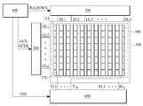
도 3은 본 발명에 따른 표시장치의 구성을 나타낸 예시도이다.3 is an exemplary view showing the configuration of a display device according to the present invention.
본 발명에 따른 표시장치는, 도 3에 도시된 바와 같이, 게이트 라인들(GL1 to GLg), 데이터 라인들(DL1 to DLd), 상기 게이트 라인들에 나란한 제1터치전극(1TE)들, 및 상기 게이트 라인들에 수직한 제2터치전극(2TE)들이 배치되어 있는 액정표시패널(500), 영상출력기간에는 상기 제1터치전극(1TE)들 및 상기 제2터치전극(2TE)들로 공통전압을 공급하며, 터치감지기간에는 상기 제1터치전극(1TE)들 및 상기 제2터치전극(2TE)들을 이용하여 터치를 감지하는 터치 센싱부(600), 기 설정된 슬루율을 갖는 적어도 두 개 이상의 게이트 클럭(GCLK)들을 생성하는 제어부(400), 상기 영상출력기간에, 상기 게이트 클럭(GCLK)들을 이용하여 게이트 펄스를 생성하며, 상기 게이트 라인들로 상기 게이트 펄스를 순차적으로 출력하는 게이트 드라이버(200), 및 상기 영상출력기간에, 상기 제어부(400)로부터 전송된 데이터 제어신호(DCS)에 따라, 상기 데이터 라인들로 데이터 전압들을 공급하는 데이터 드라이버(300)를 포함한다. 상기 제1터치전극과 상기 제2터치전극을 총칭하여 터치패널(500)이라 한다.
A display device according to the present invention includes, as shown in FIG. 3 , gate lines GL1 to GLg, data lines DL1 to DLd, first touch electrodes 1TE parallel to the gate lines, and The liquid
첫째, 상기 액정표시패널(100)은, 제1기판과 제2기판이 합착되어 형성된다. 상기 제1기판과 상기 제2기판 사이에는 중간층이 형성되어 있다.First, the liquid
상기 제1기판과 상기 제2기판은 글래스(Glass), 플라스틱(Plastic), 메탈(Metal) 등을 이용하여 제조될 수 있다. 상기 중간층은 액정(Liquid Crystal)을 포함한다.The first substrate and the second substrate may be manufactured using glass, plastic, metal, or the like. The intermediate layer includes a liquid crystal.
상기 제1기판에는, 복수의 상기 데이터 라인들(DL1 to DLd), 복수의 상기 게이트 라인들(GL1 to GLg), 상기 액정표시패널에 형성되는 픽셀들 각각에 형성되는 박막트랜지스터(TFT: Thin FilmTransistor), 상기 픽셀들 각각에 형성되어 있으며 상기 픽셀들 각각에 데이터 전압을 충전시키기 위한 픽셀전극들 및 상기 픽셀전극과 함께 상기 픽셀에 충전된 액정을 구동하기 위한 공통전극들이 형성된다.On the first substrate, a plurality of the data lines DL1 to DLd, a plurality of the gate lines GL1 to GLg, and a thin film transistor (TFT) are formed on each of the pixels formed in the liquid crystal display panel. ), pixel electrodes for charging a data voltage to each of the pixels and common electrodes for driving the liquid crystal charged in the pixel together with the pixel electrode are formed in each of the pixels.
예를 들어, 상기 데이터 라인들(DL1 to DLd)과 상기 게이트 라인들(GL1 to GLg)이 교차하는 영역마다, 상기 픽셀들이 매트릭스 형태로 배치되며, 상기 픽셀들 각각에는, 상기 TFT, 상기 픽셀전극 및 상기 공통전극이 형성된다.For example, in each region where the data lines DL1 to DLd and the gate lines GL1 to GLg intersect, the pixels are arranged in a matrix form, and in each of the pixels, the TFT and the pixel electrode and the common electrode is formed.
상기 게이트 라인들 각각으로는, 상기 게이트 드라이버(200)로부터 게이트 펄스가 공급된다.A gate pulse is supplied from the
상기 데이터 라인들 각각으로는, 상기 데이터 드라이버(300)로부터 데이터 전압이 공급된다.A data voltage is supplied from the
상기 제1기판에는, 상기 게이트 라인들(GL1 to GLg)에 나란한 제1터치전극(1TE)들 및 상기 게이트 라인들(GL1 to GLg)에 수직한 제2터치전극들(2TE)이 배치된다.First touch electrodes 1TE parallel to the gate lines GL1 to GLg and second touch electrodes 2TE perpendicular to the gate lines GL1 to GLg are disposed on the first substrate.
상기 제1터치전극(1TE)들 및 상기 제2터치전극(2TE)들 각각은, 공통전극과 터치센서의 기능을 수행한다.Each of the first touch electrodes 1TE and the second touch electrodes 2TE functions as a common electrode and a touch sensor.
예를 들어, 영상출력기간에, 상기 제1터치전극(1TE)들 및 상기 제2터치전극(2TE)들로는 공통전압이 공급된다. 터치감지기간에, 상기 제1터치전극(1TE)들 또는 상기 제2터치전극(2TE)들로 순차적으로 터치구동신호가 공급되며, 상기 제2터치전극(2TE)들 또는 상기 제1터치전극(1TE)들은 상기 터치 센싱부(600)로 감지신호를 전송한다.For example, in the image output period, a common voltage is supplied to the first touch electrodes 1TE and the second touch electrodes 2TE. During the touch sensing period, a touch driving signal is sequentially supplied to the first touch electrodes 1TE or the second touch electrodes 2TE, and the second touch electrodes 2TE or the first touch electrode 2TE 1TE) transmits a sensing signal to the
이를 위해, 상기 제1터치전극들 및 제2터치전극들은, 터치전극라인들(TL1 to TLk, RL1 to RLs)을 통해 상기 터치 센싱부(600)와 전기적으로 연결된다.
To this end, the first touch electrodes and the second touch electrodes are electrically connected to the
둘째, 상기 제어부(400)는 외부시스템(미도시)으로부터 데이터 인에이블 신호(Data Enable, DE), 도트 클럭 등의 타이밍 신호를 입력받아, 상기 데이터 드라이버(300)와 상기 게이트 드라이버(200)의 동작 타이밍을 제어하기 위한 제어신호들(GCS, DCS)을 발생한다. 또한, 상기 제어부(400)는 상기 외부시스템으로부터 입력된 입력영상데이터를 재정렬하여, 재정렬된 영상데이터(R,G,B)를 상기 데이터 드라이버(300)로 출력한다. 상기 제어부(400)는, 상기 터치 센싱부(600)의 동작 타이밍을 제어하기 위한 터치동기신호(TSS)를 생성하여, 상기 터치 센싱부(600)를 제어할 수도 있다.Second, the
예를 들어, 상기 제어부(400)는, 상기 터치패널(500)이 상기 액정표시패널(100)에 내장되어 있는 경우, 영상이 출력되는 영상출력기간과 터치가 감지되는 터치감지기간이 반복될 수 있도록, 상기 터치동기신호(TCS)를 생성하여 상기 터치 센싱부(600)로 전송할 수 있다.For example, when the
특히, 상기 제어부(400)는, 기 설정된 슬루율을 갖는 적어도 두 개 이상의 게이트 클럭들을 생성하여, 상기 게이트 드라이버(200)로 전송한다.
In particular, the
셋째, 상기 데이터 드라이버(300)는 상기 제어부(400)로부터 입력된 상기 영상데이터를 데이터 전압으로 변환하여, 상기 게이트 라인에 게이트 펄스가 공급되는 1수평기간마다 1수평라인분의 데이터 전압들을 상기 데이터 라인들에 공급한다.Third, the
예를 들어, 상기 데이터 드라이버(300)는 감마전압 발생부(미도시)로부터 공급되는 감마전압들을 이용하여, 상기 영상데이터를 데이터 전압으로 변환시킨 후, 상기 데이터 전압을 상기 데이터 라인들로 출력시킨다.
For example, the
넷째, 상기 게이트 드라이버(200)는 상기 제어부(400)로부터 전송되어온 게이트 스타트 펄스를 게이트 쉬프트 클럭에 따라 쉬프트시켜, 순차적으로 상기 게이트 라인들(GL1 to GLg)에 게이트 펄스를 공급한다.Fourth, the
특히, 상기 게이트 드라이버(200)는, 상기 제어부(400)로부터 전송되어온 상기 게이트 클럭들을 이용하여 상기 게이트 펄스를 생성한다.
In particular, the
상기 설명에서는, 상기 데이터 드라이버(300), 상기 게이트 드라이버(200) 및 상기 제어부(400)가 독립적으로 구성된 것으로서 설명되었으나, 상기 데이터 드라이버(300) 또는 상기 게이트 드라이버(200)들 중 적어도 어느 하나는 상기 제어부(400)에 구성될 수도 있다.
In the above description, the
다섯째, 상기 터치 센싱부(600)는, 상기 터치패널(500)로부터 수신되는 감지신호들을 이용하여 상기 터치패널(500)에서의 터치여부를 감지하는 기능을 수행한다.Fifth, the
상기 제1터치전극과 상기 제2터치전극을 포함하는 상기 터치패널(500)은 정전용량 방식을 이용하는 것으로서, 상기 액정표시패널(100)에 형성된다.The
특히, 상기 터치패널(500)은 뮤추얼 방식으로 구성된다. 상기 뮤추얼 방식을 이용하는 상기 터치패널(500)은 터치구동신호가 공급되는 구동전극들 및 상기 터치구동신호에 의해 생성된 감지신호를 상기 터치 센싱부(600)로 전송하는 수신전극들을 포함한다.In particular, the
상기 제1터치전극(1TE)이 상기 구동전극인 경우, 상기 제2터치전극(2TE)은 상기 수신전극이된다. 상기 제1터치전극(1TE)이 상기 수신전극인 경우, 상기 제2터치전극(2TE)은 상기 구동전극이 된다.When the first touch electrode 1TE is the driving electrode, the second touch electrode 2TE becomes the receiving electrode. When the first touch electrode 1TE is the receiving electrode, the second touch electrode 2TE becomes the driving electrode.
상기 제1터치전극들 및 상기 제2터치전극들은, 상기 터치전극라인들(TL1 to TLk, RL1 to RLs)을 통해 상기 터치 센싱부(600)와 전기적으로 연결된다.The first touch electrodes and the second touch electrodes are electrically connected to the
상기 제1터치전극들 및 상기 제2터치전극들은, 상기 영상출력기간에는 상기 공통전압이 공급되는 상기 공통전극의 기능을 수행하고, 상기 터치감지기간에는 상기 터치패널의 기능을 수행한다.The first touch electrodes and the second touch electrodes function as the common electrode to which the common voltage is supplied during the image output period, and perform the function of the touch panel during the touch sensing period.
따라서, 상기 터치 센싱부(600)는, 영상출력기간에는 상기 제1터치전극들 및 상기 제2터치전극들로 공통전압을 공급하며, 터치감지기간에는 상기 제1터치전극들 또는 상기 제2터치전극들로 순차적으로 터치구동신호를 공급하고, 상기 제2터치전극들 또는 상기 제2터치전극들로부터 수신되는 감지신호를 수신하여 터치를 감지한다.Accordingly, the
상기 터치 센싱부(600)의 구성 및 기능은, 인셀 터치 방식의 액정표시장치에 적용되는 터치 센싱부의 구성 및 기능이 그대로 적용될 수 있다. 따라서, 상기 터치 센싱부(600)의 구성 및 기능에 대한 상세한 설명은 생략된다.The configuration and function of the
상기 터치 센싱부(600)는, 도 3에 도시된 바와 같이, 상기 제어부(400) 및 상기 데이터 드라이버(300)와 독립적으로 구성될 수도 있으나, 상기 제어부(400) 또는 상기 데이터 드라이버(300)에 포함될 수도 있다.
As shown in FIG. 3 , the
도 4는 본 발명에 따른 액정표시장치에 적용되는 게이트 클럭들 간의 간격을 나타낸 예시도이다. 특히, 도 4의 (a)는 게이트 클럭들 간의 간격(G1)이 큰 경우를 나타내며, 도 4의 (b)는 게이트 클럭들 간의 간격(G2)이 작은 경우를 나타낸다. 도 5는 본 발명에 따른 액정표시장치에 적용되는 게이트 클럭들 간의 간격에 따른 게이트 클럭들 간의 휘도차이를 나타낸 일실시예 그래프이다. 예를 들어, 도 5는 게이트 클럭들 간의 간격(GCLK GAP)을 조절하면서, 카메라(예를 들어, 라디언트(Radiant) 카메라)로 촬영된 값을 이용하여, 상기 액정표시패널의 수직라인과 수평라인의 휘도차이(VSFOM)를 나타낸 그래프이다.4 is an exemplary diagram illustrating an interval between gate clocks applied to a liquid crystal display according to the present invention. In particular, FIG. 4A shows a case where the interval G1 between gate clocks is large, and FIG. 4B shows a case where the interval G2 between gate clocks is small. 5 is a graph illustrating a luminance difference between gate clocks according to an interval between gate clocks applied to a liquid crystal display according to an embodiment of the present invention. For example, FIG. 5 shows vertical lines and horizontal lines of the liquid crystal display panel using values captured by a camera (eg, a Radiant camera) while adjusting the GCLK GAP between gate clocks. It is a graph showing the difference in luminance (VSFOM) of lines.
종래기술에서 언급된 바와 같이, 상기 액정표시패널의 수직방향으로 형성된 터치전극들에 대응되는 픽셀들과, 상기 액정표시패널의 수평방향으로 형성된 터치전극들에 대응되는 픽셀들 사이에서 휘도 차이가 발생되며, 이러한 휘도 차이에 의해, 상기 패널(50)의 가로 방향 또는 세로 방향을 따라 줄무늬가 발생된다.As mentioned in the prior art, a difference in luminance occurs between pixels corresponding to the touch electrodes formed in the vertical direction of the liquid crystal display panel and pixels corresponding to the touch electrodes formed in the horizontal direction of the liquid crystal display panel. and, due to the difference in luminance, stripes are generated along the horizontal or vertical direction of the
본 발명의 발명자들은, 시뮬레이션 및 실험결과, 상기 제어부(400)로부터 상기 게이트 드라이버(200)로 전송되는 상기 게이트 클럭들의 간격을 조절함으로써, 상기 액정표시패널(100)의 수직라인과 수평라인의 휘도차이가 제어될 수 있다는 것을 알아내었다.The inventors of the present invention, as a result of simulation and experiment, by adjusting the interval between the gate clocks transmitted from the
예를 들어, 도 4의 (a)에 도시된 바와 같이, 상기 게이트 클럭들(GCLK1, GCLK2) 간의 간격(G1)이 1.5us 정도로 큰 경우에는, 상기 수직라인의 휘도가 상기 수평라인의 휘도보다 크다. 이 경우, 상기 간격(G1)은, 도 5에 도시된 그래프의 세로축값(VSFOM)이 양의 값을 갖는 게이트 클럭들 간의 간격들에 포함된다.For example, as shown in (a) of FIG. 4 , when the interval G1 between the gate clocks GCLK1 and GCLK2 is as large as 1.5 μs, the luminance of the vertical line is higher than the luminance of the horizontal line. Big. In this case, the interval G1 is included in intervals between gate clocks in which the vertical axis value VSFOM of the graph shown in FIG. 5 has a positive value.
또한, 도 4의 (b)에 도시된 바와 같이, 상기 게이트 클럭들(GCLK1, GCLK2) 간의 간격(G2)이 0.8us 정도로 작은 경우에는, 상기 수직라인의 휘도가 상기 수평라인의 휘도보다 작다. 이 경우, 상기 간격(G2)은, 도 5에 도시된 그래프의 세로축값(VSFORM)이 음의 값을 갖는 게이트 클럭들 간의 간격들에 포함된다.Also, as shown in FIG. 4B , when the interval G2 between the gate clocks GCLK1 and GCLK2 is as small as 0.8 us, the luminance of the vertical line is smaller than the luminance of the horizontal line. In this case, the interval G2 is included in intervals between gate clocks in which the vertical axis value VSFORM of the graph shown in FIG. 5 has a negative value.
이 경우, 상기 수직라인의 휘도와 상기 수평라인의 휘도 차이가 0인 지점에서의 게이트 클럭들 간의 간격(X)을 갖도록, 상기 게이트 드라이버(200)로 전송되는 게이트 클럭들의 간격이 제어되면, 상기한 바와 같은 휘도차이가 발생되지 않을 수 있다.In this case, when the interval between the gate clocks transmitted to the
그러나, 상기 수직라인의 휘도와 상기 수평라인의 휘도 차이가 0인 지점에서의 게이트 클럭들 간의 간격(X)을 갖도록, 상기 게이트 드라이버(200)로 전송되는 게이트 클럭들의 간격이 제어된 액정표시패널이라 하더라도, 상기 액정표시패널이 지속적으로 사용됨에 따라, 상기 휘도차이가 발생될 수 있다.However, the liquid crystal display panel in which the interval between the gate clocks transmitted to the
예를 들어, 도 5에서 A로 표시된 그래프는, 상기 액정표시패널의 제조 공정 중에서 분석된 휘도차이를 나타내며, B로 표시된 그래프는, 상기 액정표시패널이 장시간 동안 사용된 이후에 분석된 휘도차이를 나타낸다. 부연하여 설명하면, A로 표시된 그래프에서 휘도 차이가 0인 X 지점에서의 게이트 클럭들 간의 간격(X)을 갖도록 상기 게이트 드라이버(200)로 전송되는 게이트 클럭들의 간격이 제어되더라도, 상기 액정표시패널이 지속적으로 사용되면, 상기 X 지점에서의 휘도 차이가 변경된다. 따라서, 액정표시패널이 지속적으로 사용되면, 상기 수직라인의 휘도가 상기 수평라인의 휘도보다 작아져, 상기 수평라인이 사용자의 눈에 보여진다.
For example, the graph indicated by A in FIG. 5 represents the luminance difference analyzed during the manufacturing process of the liquid crystal display panel, and the graph indicated by B indicates the luminance difference analyzed after the liquid crystal display panel has been used for a long time. indicates. In detail, even if the interval between the gate clocks transmitted to the
도 6은 본 발명에 따른 액정표시장치에 적용되는 게이트 클럭들 간의 간격을 나타낸 또 다른 예시도이며, 도 7은 본 발명에 따른 액정표시장치에 적용되는 게이트 클럭의 슬루율을 설명하는 예시도이다.6 is another exemplary diagram illustrating an interval between gate clocks applied to a liquid crystal display device according to the present invention, and FIG. 7 is an exemplary diagram illustrating a slew rate of a gate clock applied to a liquid crystal display device according to the present invention. .
게이트 클럭들 간의 간격이 큰 영역(Y)에서는, 도 5에 도시된 바와 같이,A로 표시된 그래프에서의 휘도차이와, B로 표시된 그래프에서의 휘도차이가 거의 비슷하다.In the region Y where the interval between gate clocks is large, as shown in FIG. 5 , the luminance difference in the graph indicated by A and the luminance difference in the graph indicated by B are almost the same.
이것은, 게이트 클럭들 간의 간격이 크면, 상기 게이트 클럭들이 공급되는 액정표시패널이 장시간 사용되더라도, 수직라인과 수평라인의 휘도차이가 적다는 것을 의미한다.This means that if the interval between the gate clocks is large, even if the liquid crystal display panel to which the gate clocks are supplied is used for a long time, the difference in luminance between the vertical line and the horizontal line is small.
따라서, 액정표시패널의 제조 공정 중에 분석되어 A로 표시된 그래프가, 도 6에서, C로 표시된 그래프로 변경될 수 있다면, 상기 Y 영역에 포함되는 간격을 갖는 게이트 클럭들을 이용하는 액정표시패널이 장시간 사용되더라도, 수직라인과 수평라인의 휘도차이가 발생되지 않는다.Therefore, if the graph indicated by A after being analyzed during the manufacturing process of the liquid crystal display panel can be changed to the graph indicated by C in FIG. 6 , the liquid crystal display panel using gate clocks having an interval included in the Y region is used for a long time. However, there is no difference in luminance between the vertical line and the horizontal line.
각종 시뮬레이션 및 실험결과, 도 7에 도시된 바와 같이, 게이트 클럭(GCLK)의 슬루율을 변경하는 것에 의해, 도 6에서 A로 표시된 그래프가, C로 표시된 그래프로 변경될 수 있음이 확인되었다.As a result of various simulations and experiments, as shown in FIG. 7 , it was confirmed that the graph indicated by A in FIG. 6 can be changed to the graph indicated by C by changing the slew rate of the gate clock GCLK.
예를 들어, 게이트 클럭의 슬루율이 0인 경우, 도 7에서, 게이트 클럭(GCLK)은 X1 및 Y1으로 표시된 파형을 갖고, 게이트 클럭의 슬루율이 조금 더 커지면, 게이트 클럭(GCLK)은 X2 및 Y2로 표시된 파형을 가지며, 게이트 클럭의 슬루율이 더 커지면, 게이트 클럭(GCLK)은 Xn 및 Yn으로 표시된 파형을 갖는다.For example, when the slew rate of the gate clock is 0, in FIG. 7 , the gate clock GCLK has waveforms indicated by X1 and Y1, and when the slew rate of the gate clock becomes slightly larger, the gate clock GCLK becomes X2 and Y2, and when the slew rate of the gate clock becomes larger, the gate clock GCLK has waveforms denoted by Xn and Yn.
따라서, 게이트 클럭들 간의 간격을 최대한 크게하고, 게이트 클럭의 슬루율을 변경하면, 액정표시패널이 장시간 사용되더라도, 수직라인과 수평라인의 휘도차이가 발생되지 않는다.Accordingly, if the interval between the gate clocks is maximized and the slew rate of the gate clock is changed, even if the liquid crystal display panel is used for a long time, a difference in luminance between the vertical line and the horizontal line is not generated.
이를 위해, 액정표시패널의 제조 과정에서의 검사 공정을 통해, 도 6에서 C로표시된 그래프를 갖도록 하는 게이트 클럭의 슬루율 및 게이트 클럭들 간의 간격이 파악되어야 한다.To this end, the slew rate of the gate clock and the interval between the gate clocks to have the graph indicated by C in FIG. 6 should be identified through the inspection process in the manufacturing process of the liquid crystal display panel.
첫째, 액정표시패널이 제조되면, 검사장비를 이용하여, 상기 액정표시패널로, 다양한 간격을 갖는 게이트 클럭들이 공급된다. 상기 검사장비를 이용하여, 도 6에서 Y 영역에 포함되는 게이트 클럭들 간의 간격이 산출될 수 있다.First, when a liquid crystal display panel is manufactured, gate clocks having various intervals are supplied to the liquid crystal display panel using inspection equipment. The interval between gate clocks included in the Y region in FIG. 6 may be calculated using the inspection equipment.
둘째, 검사장비를 이용하여, 상기 액정표시패널로, 다양한 슬루율을 갖는 게이트 클럭들이 공급된다. 상기 검사장비를 이용하여, 도 6에서 C로 표현되는 그래프에 대응되는 슬루율이 산출될 수 있다. C로 표현된 그래프는, 상기 Y영역에서의 수직라인과 수평라인 간의 휘도차이가 0에 가까운 값을 갖는다.
Second, gate clocks having various slew rates are supplied to the liquid crystal display panel using inspection equipment. Using the inspection equipment, a slew rate corresponding to a graph represented by C in FIG. 6 may be calculated. In the graph represented by C, the difference in luminance between the vertical line and the horizontal line in the Y region has a value close to zero.
도 8은 본 발명에 따른 액정표시장치에 적용되는 제어부와 게이트 드라이버의 구성을 나타낸 예시도이며, 도 9는 도 8에 도시된 제어부의 구성을 세부적으로 나타낸 예시도이다.8 is an exemplary diagram illustrating the configuration of a control unit and a gate driver applied to a liquid crystal display device according to the present invention, and FIG. 9 is an exemplary diagram showing the configuration of the control unit shown in FIG. 8 in detail.
본 발명에 따른 액정표시장치에 적용되는 상기 제어부(400)는, 기 설정된 슬루율을 갖는 적어도 두 개 이상의 게이트 클럭들을 생성한다. 이하에서는, 도 8 및 도 9에 도시된 바와 같이, 두 개의 게이트 클럭들(GCLK1, GCLK2)을 생성하는 제어부(400) 및 상기 두 개의 게이트 클럭들을 이용하여 게이트 펄스를 생성하는 게이트 드라이버(200)를 포함하는 액정표시장치가, 본 발명의 일예로서 설명된다.The
상기 제어부(400)는, 상기 외부시스템으로부터 입력영상데이터(Input RGB) 및 상기 타이밍 신호(TS)를 입력받는 입력부(410), 상기 타이밍 신호(TS)를 이용하여 각종 제어신호를 생성하는 제어신호 생성부(430), 상기 입력영상데이터를 상기 영상데이터(RGB)로 변환하여 상기 데이터 드라이버(300)로 전송하는 입력영상 변환부(420) 및 상기 기 설정된 슬루율을 결정하는 적어도 두 개의 슬루율 제어신호들(SCS1, SCS2)을 저장하는 저장부(440)를 포함한다.The
상기 제어신호 생성부(430)는 상기 데이터 제어신호(DCS)를 생성하는 데이터 제어신호 생성부(432) 및 상기 슬루율 제어신호(SCS)들을 이용하여, 적어도 두 개의 가변저항들(VR1, VR2)의 저항값을 변경하여, 상기 게이트 클럭들(GCLK1, GCLK2)을 생성하는 게이트 클럭 생성부(431)를 포함한다. 상기 게이트 클럭 생성부(431)는 상기 게이트 제어신호(GCS)를 생성할 수 있다. 그러나, 상기 제어신호 생성부(430)는 상기 게이트 제어신호(GCS)를 생성하는 게이트 제어신호 생성부를 별도로 포함할 수 있다.
The
첫째, 상기 게이트 클럭(GCLK)들은, 기 설정된 간격을 갖는다.First, the gate clocks GCLK have a predetermined interval.
상기 게이트 클럭들(GCLK1, GCLK2) 간의 간격은, 상기 게이트 클럭들 간의 간격에 따른, 상기 제2터치전극 영역과 상기 제1터치전극 영역 간의 밝기 차이를 나타내는 그래프에서, 상기 제2터치전극 영역이 상기 제1터치전극 영역보다 밝게 나타나는 영역에 포함된, 상기 게이트 클럭들 간의 간격들 중 어느 하나이다.The interval between the gate clocks GCLK1 and GCLK2 is, in the graph representing the difference in brightness between the second touch electrode region and the first touch electrode region, according to the interval between the gate clocks, the second touch electrode region Any one of the intervals between the gate clocks included in a region that appears brighter than the first touch electrode region.
부연하여 설명하면, 상기 게이트 클럭들(GCLK1, GCLK2) 간의 간격은, 도 6에서 Y 영역에 포함되는 간격을 갖는다. 상기 간격은 상기에서 설명된 바와 같이, 액정표시패널의 제조 공정에서, 각종 검사장비를 통해 산출될 수 있다.
In more detail, the interval between the gate clocks GCLK1 and GCLK2 is the interval included in the Y region in FIG. 6 . As described above, the interval may be calculated through various inspection equipment in the manufacturing process of the liquid crystal display panel.
둘째, 상기 게이트 클럭 생성부(431)는, 상기 슬루율 제어신호들(SCS1, SCS2)을 이용하여, 적어도 두 개의 가변저항들(VR1, VR2)의 저항값을 변경하여, 클럭들(CLK1, CLK2)을 생성하는 적어도 두 개 이상의 생성기(431a)들 및 상기 저장부(440)로부터 전송되는 간격 제어신호(GCS)를 이용하여, 상기 클럭들(CLK1, CLK2)을 지연시켜, 상기 기 설정된 간격을 갖는 상기 게이트 클럭들(GCLK1, GCLK2)을 생성하는 지연기(431b)를 포함한다.Second, the
우선, 상기 저장부(440)에는, 두 개의 상기 슬루율 제어신호들(SCS1, SCS2)이 저장된다. 상기 슬루율 제어신호들은, 상기에서 설명된 바와 같이, 액정표시패널의 제조 공정에서, 각종 검사장비를 통해 산출될 수 있다. 부연하여 설명하면, 상기 슬루율 제어신호들은, 도 6에서 C로 표시된 그래프에 대응되는 게이트 클럭들을 생성하기 위한 값이다. 예를 들어, 제1슬루율 제어신호(SCS1)는, 도 9에 도시된 상기 생성기(431a)의 제1가변저항(VR1)을 특정값으로 변경시키는 신호이며, 제2슬루율 제어신호(SCS2)는, 상기 생성기(431b)의 제2가변저항(VR2)을 특정값을 변경시키는 신호이다.First, the
다음, 상기 생성기(431a)들 각각은 상기 슬루율 제어신호들(SCS1, SCS2)을 이용하여, 적어도 두 개의 가변저항들(VR1, VR2)의 저항값을 변경하여, 상기 클럭을 생성한다. 예를 들어, 도 9에 도시된 두 개의 상기 생성기(431a)들 중, 어느 하나는 제1클럭(CLK1)을 생성하며, 나머지 하나의 상기 생성기(431a)는 제2클럭(CLK2)을 생성한다.Next, each of the
상기 제1클럭(CLK1)과 상기 제2클럭(CLK2) 각각은 상기 기 설정된 슬루율을 갖는다.Each of the first clock CLK1 and the second clock CLK2 has the preset slew rate.
마지막으로, 상기 지연기(431b)는, 상기 간격 제어신호(GCS)를 이용하여, 상기 클럭들(CLK1, CLK2)을 지연시켜, 상기 기 설정된 간격을 갖는 상기 게이트 클럭들(GCLK1, GCLK2)을 생성한다.Finally, the
따라서, 상기 두 개의 게이트 클럭들(GCLK1, GCLK2) 각각은 상기 기 설정된 슬루율을 가지며, 상기 두 개의 게이트 클럭은 상기 기 설정된 간격을 갖는다.Accordingly, each of the two gate clocks GCLK1 and GCLK2 has the preset slew rate, and the two gate clocks have the preset interval.
상기 지연기(431b)는, 현재 각종 회로에서, 신호를 지연시키기 위해 이용되는 지연기가 적용될 수 있다.
The
셋째, 상기 생성기(431a)들 각각은, 도 9에 도시된 바와 같이, 게이트 하이 전압(VGH)이 공급되는 하이전압단자(H) 및 상기 클럭(CLK)이 출력되는 출력단자(OUT) 사이에 연결되고, 제1전압에 의해 턴온되는 제1트랜지스터(T1), 게이트 로우 전압(VGL)이 공급되는 로우전압단자(L) 및 상기 출력단자(OUT) 사이에 연결되고, 제2전압에 의해 턴온되는 제2트랜지스터(T2), 상기 하이전압단자(H) 및 상기 제1트랜지스터(T1) 사이에 연결되며, 상기 저장부(440)로부터 전송되는 제1슬루율 제어신호(SCS1)에 따라 저항값이 가변되는 제1가변저항(VR1) 및 상기 로우전압단자(L) 및 상기 제2트랜지스터(T2) 사이에 연결되며, 상기 저장부(440)로부터 전송되는 제2슬루율 제어신호(SCS2)에 따라 저항값이 가변되는 제2가변저항(VR2)을 포함한다.Third, each of the
우선, 상기 게이트 하이 전압(VGH)은 상기 게이트 펄스의 하이 레벨에 대응되는 값을 갖는다. 상기 게이트 로우 전압(VGL)은 상기 게이트 펄스의 로우 레벨에 대응되는 값을 갖는다.First, the gate high voltage VGH has a value corresponding to the high level of the gate pulse. The gate low voltage VGL has a value corresponding to the low level of the gate pulse.
다음, 상기 제1트랜지스터(T1)는, 상기 하이전압단자(H) 및 상기 출력단자(OUT) 사이에 연결되고, 제1전압에 의해 턴온된다. 상기 제1전압은, 직류입력전압(IN1)을 레벨 쉬프터(L/S)로 승압시켜 생성되며, 상기 제1트랜지스터(T1)의 게이트로 입력되어, 상기 제1트랜지스터(T1)를 턴온 또는 턴오프시킨다. 상기 제1트랜지스터(T1)는 P타입 트랜지스터가 될 수 있다.Next, the first transistor T1 is connected between the high voltage terminal H and the output terminal OUT, and is turned on by the first voltage. The first voltage is generated by boosting the DC input voltage IN1 with the level shifter L/S, is input to the gate of the first transistor T1, and turns on or turns on the first transistor T1 turn it off The first transistor T1 may be a P-type transistor.
다음, 상기 제2트랜지스터(T2)는 상기 로우전압단자(L) 및 상기 출력단자(OUT) 사이에 연결되고, 제2전압에 의해 턴온된다. 상기 제2전압은, 직류입력전압(IN2)을 레벨 쉬프터(L/S)로 승압시켜 생성되며, 상기 제2트랜지스터(T2)의 게이트로 입력되어, 상기 제2트랜지스터(T2)를 턴온 또는 턴오프시킨다. 상기 제1트랜지스터(T2)는 N타입 트랜지스터가 될 수 있다. 부연하여 설명하면, 상기 제1트랜지스터(T1)와 상기 제2트랜지스터(T2)는 서로 다른 타입으로 형성될 수 있다.Next, the second transistor T2 is connected between the low voltage terminal L and the output terminal OUT, and is turned on by a second voltage. The second voltage is generated by boosting the DC input voltage IN2 with the level shifter L/S, is input to the gate of the second transistor T2, and turns on or turns on the second transistor T2 turn it off The first transistor T2 may be an N-type transistor. In more detail, the first transistor T1 and the second transistor T2 may be formed in different types.
다음, 상기 제1가변저항(VR1)은, 상기 하이전압단자(H) 및 상기 제1트랜지스터(T1) 사이에 연결되며, 상기 저장부(440)로부터 전송되는 제1슬루율 제어신호(SCS1)에 따라 저항값이 가변된다.Next, the first variable resistor VR1 is connected between the high voltage terminal H and the first transistor T1 and a first slew rate control signal SCS1 transmitted from the
다음, 상기 제2가변저항(VR2)은, 상기 로우전압단자(L) 및 상기 제2트랜지스터(T2) 사이에 연결되며, 상기 저장부(440)로부터 전송되는 제2슬루율 제어신호(SCS2)에 따라 저항값이 가변된다.Next, the second variable resistor VR2 is connected between the low voltage terminal L and the second transistor T2 , and a second slew rate control signal SCS2 is transmitted from the
마지막으로, 상기 출력단자(OUT)를 통해서, 상기 제1클럭(CLK1) 또는 상기 제2클럭(CLK2)이 출력되어, 상기 지연기(431b)로 공급된다.Finally, the first clock CLK1 or the second clock CLK2 is output through the output terminal OUT and supplied to the
상기 생성기(431a)가 상기 클럭의 슬루율을 변경시키는 원리를 간단히 설명하면 다음과 같다.A principle of the
예를 들어, RC 회로에서 시정수는 t = R x C 이며, R(저항값)과 시정수는 비례 관계이다. 여기서, 저항값이 커지면, 입력전압의 도달시간이 늘어지게 된다. 따라서, 상기 저항값을 변경하는 것에 의해 상기 클럭의 슬루율이 변경될 수 있다.For example, in an RC circuit, the time constant is t = R x C, and R (resistance value) and the time constant are proportional. Here, as the resistance value increases, the arrival time of the input voltage increases. Accordingly, the slew rate of the clock may be changed by changing the resistance value.
이에 따라, 본 발명에서는, 상기 슬루율 제어신호들(SCS1, SCS2)에 따라, 상기 가변저항의 저항값을 변경하여, 상기 클럭들(CLK1, CLK2)의 슬루율을 변경시킨다.Accordingly, in the present invention, the slew rate of the clocks CLK1 and CLK2 is changed by changing the resistance value of the variable resistor according to the slew rate control signals SCS1 and SCS2.
상기 지연기(431b)에서는 상기 클럭들간의 간격만이 조절된다. 따라서, 상기 지연기(431b)로부터 출력되는 상기 게이트 클럭들은, 상기 생성기(431a)에서 설정된 슬루율을 갖는다.
In the
넷째, 상기 게이트 드라이버(200)는, 도 8에 도시된 바와 같이, 복수의 스테이지들(1state to gstage)을 포함한다. 상기 게이트 드라이버(200)는, 상기 게이트 라인들(GL1 to GLg)로 게이트 펄스들(GP1 to GPg)을 순차적으로 출력한다.Fourth, the
상기 스테이지(210)들 각각은, 상기 게이트 라인과 연결된다. 상기 스테이지(210)는, 상기 게이트 클럭 생성부(431)로부터 전송된 상기 게이트 클럭들(GCLK1, GCL2)을 이용하여 상기 게이트 펄스(GP)를 생성하며, 생성된 상기 게이트 펄스를 상기 게이트 라인으로 출력한다.Each of the
상기한 바와 같은 본 발명에 의하면, 게이트 라인들과 수직하게 형성되어 있는 터치전극들을 따라, 줄무늬가 발생되지 않는다.According to the present invention as described above, stripes are not generated along the touch electrodes formed perpendicular to the gate lines.
본 발명이 속하는 기술분야의 당업자는 본 발명이 그 기술적 사상이나 필수적 특징을 변경하지 않고서 다른 구체적인 형태로 실시될 수 있다는 것을 이해할 수 있을 것이다. 그러므로, 이상에서 기술한 실시 예들은 모든 면에서 예시적인 것이며 한정적인 것이 아닌 것으로 이해해야만 한다. 본 발명의 범위는 상기 상세한 설명보다는 후술하는 특허청구범위에 의하여 나타내어지며, 특허청구범위의 의미 및 범위 그리고 그 등가 개념으로부터 도출되는 모든 변경 또는 변형된 형태가 본 발명의 범위에 포함되는 것으로 해석되어야 한다.Those skilled in the art to which the present invention pertains will understand that the present invention may be embodied in other specific forms without changing the technical spirit or essential characteristics thereof. Therefore, it should be understood that the embodiments described above are illustrative in all respects and not restrictive. The scope of the present invention is indicated by the following claims rather than the above detailed description, and all changes or modifications derived from the meaning and scope of the claims and their equivalent concepts should be interpreted as being included in the scope of the present invention. do.
100 : 패널 200 : 게이트 드라이버
300 : 데이터 드라이버400 : 제어부
500 : 터치패널600 : 터치 센싱부100: panel 200: gate driver
300: data driver 400: control unit
500: touch panel 600: touch sensing unit
Claims (5)
Translated fromKorean영상출력기간에는 상기 제1터치전극들 및 상기 제2터치전극들로 공통전압을 공급하며, 터치감지기간에는 상기 제1터치전극들 및 상기 제2터치전극들을 이용하여 터치를 감지하는 터치 센싱부;
기 설정된 슬루율 및 기 설정된 간격을 갖는 적어도 두 개 이상의 게이트 클럭들을 생성하는 제어부;
상기 영상출력기간에, 상기 게이트 클럭들을 이용하여 게이트 펄스를 생성하며, 상기 게이트 라인들로 상기 게이트 펄스를 순차적으로 출력하는 게이트 드라이버; 및
상기 영상출력기간에, 상기 제어부로부터 전송된 데이터 제어신호에 따라, 상기 데이터 라인들로 데이터 전압들을 공급하고,
상기 기 설정된 간격은,
상기 게이트 클럭들 간의 간격에 따른, 상기 제2터치전극 영역과 상기 제1터치전극 영역 간의 밝기 차이를 나타내는 그래프에서, 상기 제2터치전극 영역이 상기 제1터치전극 영역보다 밝게 나타나는 영역에 포함된, 상기 게이트 클럭들 간의 간격들 중 어느 하나이며,
상기 기 설정된 슬루율은,
상기 영역에서 상기 제2 터치전극 영역과 상기 제1 터치전극 영역의 휘도차이가 발생되지 않도록 하는 슬루율들 중 어느 하나인 액정표시장치.a liquid crystal display panel having gate lines, data lines, first touch electrodes parallel to the gate lines, and second touch electrodes perpendicular to the gate lines;
a touch sensing unit that supplies a common voltage to the first touch electrodes and the second touch electrodes during an image output period, and senses a touch using the first touch electrodes and the second touch electrodes during a touch sensing period;
a control unit generating at least two gate clocks having a preset slew rate and a preset interval;
a gate driver generating a gate pulse using the gate clocks during the image output period and sequentially outputting the gate pulse to the gate lines; and
supplying data voltages to the data lines according to the data control signal transmitted from the control unit during the image output period;
The preset interval is
In the graph showing the difference in brightness between the second touch electrode area and the first touch electrode area according to the interval between the gate clocks, the second touch electrode area is included in an area that appears brighter than the first touch electrode area. , any one of the intervals between the gate clocks,
The preset slew rate is
The liquid crystal display device according to any one of slew rates for preventing a difference in luminance between the second touch electrode region and the first touch electrode region from occurring in the region.
상기 제어부는,
상기 기 설정된 슬루율을 결정하는 적어도 두 개의 슬루율 제어신호들을 저장하는 저장부; 및
상기 슬루율 제어신호들을 이용하여, 적어도 두 개의 가변저항들의 저항값을 변경하여, 상기 게이트 클럭들을 생성하는 게이트 클럭 생성부를 포함하며,
상기 게이트 클럭들은, 상기 기 설정된 간격을 갖는 액정표시장치.The method of claim 1,
The control unit is
a storage unit configured to store at least two slew rate control signals for determining the preset slew rate; and
and a gate clock generator configured to generate the gate clocks by changing resistance values of at least two variable resistors using the slew rate control signals;
The gate clocks have the predetermined interval.
상기 게이트 클럭 생성부는,
상기 슬루율 제어신호들을 이용하여, 적어도 두 개의 가변저항들의 저항값을 변경하여, 클럭들을 생성하는 적어도 두 개 이상의 생성기들; 및
상기 저장부로부터 전송되는 간격 제어신호를 이용하여, 상기 클럭들을 지연시켜, 상기 기 설정된 간격을 갖는 상기 게이트 클럭들을 생성하는 지연기를 포함하는 액정표시장치.4. The method of claim 3,
The gate clock generator,
at least two generators for generating clocks by changing resistance values of at least two variable resistors using the slew rate control signals; and
and a delay unit configured to generate the gate clocks having the preset interval by delaying the clocks using the interval control signal transmitted from the storage unit.
상기 생성기들 각각은,
게이트 하이 전압이 공급되는 하이전압단자 및 상기 클럭이 출력되는 출력단자 사이에 연결되고, 제1전압에 의해 턴온되는 제1트랜지스터;
게이트 로우 전압이 공급되는 로우전압단자 및 상기 출력단자 사이에 연결되고, 제2전압에 의해 턴온되는 제2트랜지스터;
상기 하이전압단자 및 상기 제1트랜지스터 사이에 연결되며, 상기 저장부로부터 전송되는 제1슬루율 제어신호에 따라 저항값이 가변되는 제1가변저항; 및
상기 로우전압단자 및 상기 제2트랜지스터 사이에 연결되며, 상기 저장부로부터 전송되는 제2슬루율 제어신호에 따라 저항값이 가변되는 제2가변저항을 포함하는 액정표시장치.5. The method of claim 4,
Each of the generators is
a first transistor connected between the high voltage terminal to which the gate high voltage is supplied and the output terminal to which the clock is output, the first transistor being turned on by the first voltage;
a second transistor connected between a low voltage terminal to which a gate low voltage is supplied and the output terminal and turned on by a second voltage;
a first variable resistor connected between the high voltage terminal and the first transistor, the first variable resistor having a variable resistance according to a first slew rate control signal transmitted from the storage unit; and
and a second variable resistor connected between the low voltage terminal and the second transistor, the second variable resistor having a variable resistance according to a second slew rate control signal transmitted from the storage unit.
Priority Applications (4)
| Application Number | Priority Date | Filing Date | Title |
|---|---|---|---|
| KR1020140186161AKR102283461B1 (en) | 2014-12-22 | 2014-12-22 | Liquid crystal display device |
| CN201510924478.8ACN105717680B (en) | 2014-12-22 | 2015-12-14 | Liquid crystal display device |
| EP15199746.7AEP3038095A1 (en) | 2014-12-22 | 2015-12-14 | Liquid crystal display device |
| US14/974,995US9791966B2 (en) | 2014-12-22 | 2015-12-18 | Liquid crystal display device with gate clock signals having specific slew rate |
Applications Claiming Priority (1)
| Application Number | Priority Date | Filing Date | Title |
|---|---|---|---|
| KR1020140186161AKR102283461B1 (en) | 2014-12-22 | 2014-12-22 | Liquid crystal display device |
Publications (2)
| Publication Number | Publication Date |
|---|---|
| KR20160077313A KR20160077313A (en) | 2016-07-04 |
| KR102283461B1true KR102283461B1 (en) | 2021-07-29 |
Family
ID=54979397
Family Applications (1)
| Application Number | Title | Priority Date | Filing Date |
|---|---|---|---|
| KR1020140186161AActiveKR102283461B1 (en) | 2014-12-22 | 2014-12-22 | Liquid crystal display device |
Country Status (4)
| Country | Link |
|---|---|
| US (1) | US9791966B2 (en) |
| EP (1) | EP3038095A1 (en) |
| KR (1) | KR102283461B1 (en) |
| CN (1) | CN105717680B (en) |
Families Citing this family (12)
| Publication number | Priority date | Publication date | Assignee | Title |
|---|---|---|---|---|
| CN105139824B (en)* | 2015-10-16 | 2018-02-06 | 重庆京东方光电科技有限公司 | Gate drivers and its configuration system and regulating allocation method |
| KR102620569B1 (en)* | 2016-07-29 | 2024-01-04 | 삼성디스플레이 주식회사 | Method of driving display panel and display apparatus for performing the same |
| CN106647072A (en)* | 2016-10-20 | 2017-05-10 | 深圳市华星光电技术有限公司 | Array substrate, liquid crystal displayer and display device |
| KR102545234B1 (en) | 2016-10-28 | 2023-06-19 | 삼성디스플레이 주식회사 | Display device |
| KR102645899B1 (en) | 2017-02-15 | 2024-03-11 | 삼성디스플레이 주식회사 | Display device |
| CN107219438B (en)* | 2017-07-24 | 2019-09-03 | 武汉天马微电子有限公司 | Display panel, test method thereof and display device |
| KR102482210B1 (en)* | 2017-12-28 | 2022-12-27 | 엘지디스플레이 주식회사 | Touch Device And Method Of Driving The Same |
| CN108595040B (en)* | 2018-01-02 | 2021-01-15 | 联想(北京)有限公司 | Touch display screen assembly and electronic equipment |
| CN110767134B (en)* | 2018-07-26 | 2023-05-16 | 瀚宇彩晶股份有限公司 | Slope Control Method Applicable to Gate Drive Circuit Waveform |
| US10762863B2 (en)* | 2018-09-11 | 2020-09-01 | HKC Corporation Limited | Device and method of driving display panel |
| KR102678025B1 (en)* | 2019-12-31 | 2024-06-26 | 엘지디스플레이 주식회사 | Display device and driving method thereof |
| CN114450743B (en)* | 2020-09-02 | 2023-07-25 | 京东方科技集团股份有限公司 | Driving method, driving circuit and display device |
Citations (3)
| Publication number | Priority date | Publication date | Assignee | Title |
|---|---|---|---|---|
| US20100171716A1 (en) | 2009-01-05 | 2010-07-08 | Tetsuo Ikeda | Information processing apparatus, information processing method, and program |
| US20120162121A1 (en) | 2010-12-22 | 2012-06-28 | Shih Chang Chang | Slew rate and shunting control separation |
| US20120280965A1 (en) | 2011-05-03 | 2012-11-08 | Apple Inc. | System and method for controlling the slew rate of a signal |
Family Cites Families (17)
| Publication number | Priority date | Publication date | Assignee | Title |
|---|---|---|---|---|
| KR100685307B1 (en)* | 1999-11-05 | 2007-02-22 | 엘지.필립스 엘시디 주식회사 | Shift register |
| KR100746200B1 (en)* | 2005-10-21 | 2007-08-06 | 삼성전자주식회사 | Source drivers, source driver modules, and display devices |
| KR101293559B1 (en)* | 2007-04-06 | 2013-08-06 | 삼성디스플레이 주식회사 | Touch sensible display device, and apparatus and driving method thereof |
| TWI391729B (en)* | 2008-07-16 | 2013-04-01 | Tpo Displays Corp | Liquid crystal display |
| TWI488095B (en)* | 2009-02-26 | 2015-06-11 | Genesys Logic Inc | Power down method and surface capacitive touch panel device using the same |
| KR20120014808A (en)* | 2010-08-10 | 2012-02-20 | 엘지디스플레이 주식회사 | LCD including touch sensor, driving method thereof and manufacturing method thereof |
| CN101996684B (en)* | 2010-11-10 | 2013-07-24 | 友达光电股份有限公司 | Shift register and touch device |
| WO2012147962A1 (en)* | 2011-04-28 | 2012-11-01 | シャープ株式会社 | Liquid crystal display device |
| US20130063404A1 (en)* | 2011-09-13 | 2013-03-14 | Abbas Jamshidi Roudbari | Driver Circuitry for Displays |
| KR101942984B1 (en)* | 2012-03-08 | 2019-01-28 | 엘지디스플레이 주식회사 | Gate driver and image display device including the same |
| JP5758825B2 (en)* | 2012-03-15 | 2015-08-05 | 株式会社ジャパンディスプレイ | Display device, display method, and electronic apparatus |
| US9013384B2 (en)* | 2012-06-08 | 2015-04-21 | Apple Inc. | Systems and methods for reducing or eliminating mura artifact using contrast enhanced imagery |
| KR20140036729A (en)* | 2012-09-18 | 2014-03-26 | 엘지디스플레이 주식회사 | Gate shift register and flat panel display using the same |
| KR101992158B1 (en)* | 2013-04-30 | 2019-09-30 | 엘지디스플레이 주식회사 | Gate shift register and display device using the same |
| US9530373B2 (en)* | 2013-06-25 | 2016-12-27 | Samsung Display Co., Ltd. | Method of driving a display panel, display panel driving apparatus for performing the method and display apparatus having the display panel driving apparatus |
| KR102111274B1 (en)* | 2013-09-26 | 2020-05-15 | 엘지디스플레이 주식회사 | Touch sensing system and driving method thereof |
| CN104049796B (en)* | 2014-05-19 | 2017-02-15 | 京东方科技集团股份有限公司 | Touch display screen and time-sharing drive method thereof |
- 2014
- 2014-12-22KRKR1020140186161Apatent/KR102283461B1/enactiveActive
- 2015
- 2015-12-14EPEP15199746.7Apatent/EP3038095A1/ennot_activeCeased
- 2015-12-14CNCN201510924478.8Apatent/CN105717680B/enactiveActive
- 2015-12-18USUS14/974,995patent/US9791966B2/enactiveActive
Patent Citations (4)
| Publication number | Priority date | Publication date | Assignee | Title |
|---|---|---|---|---|
| US20100171716A1 (en) | 2009-01-05 | 2010-07-08 | Tetsuo Ikeda | Information processing apparatus, information processing method, and program |
| JP2010157189A (en) | 2009-01-05 | 2010-07-15 | Sony Corp | Information processor, information processing method and program |
| US20120162121A1 (en) | 2010-12-22 | 2012-06-28 | Shih Chang Chang | Slew rate and shunting control separation |
| US20120280965A1 (en) | 2011-05-03 | 2012-11-08 | Apple Inc. | System and method for controlling the slew rate of a signal |
Also Published As
| Publication number | Publication date |
|---|---|
| US9791966B2 (en) | 2017-10-17 |
| CN105717680B (en) | 2019-04-30 |
| CN105717680A (en) | 2016-06-29 |
| KR20160077313A (en) | 2016-07-04 |
| US20160179275A1 (en) | 2016-06-23 |
| EP3038095A1 (en) | 2016-06-29 |
Similar Documents
| Publication | Publication Date | Title |
|---|---|---|
| KR102283461B1 (en) | Liquid crystal display device | |
| US10656743B2 (en) | Display apparatus | |
| TWI608388B (en) | Display device and driving method and driving circuit thereof | |
| US10665186B2 (en) | Display apparatus | |
| KR101648571B1 (en) | In-cell touch type display device | |
| JP5925279B2 (en) | Display device and driving method thereof | |
| KR102310484B1 (en) | Touch screen device | |
| TWI590122B (en) | Driver integrated circuit and display apparatus including the same | |
| KR102295877B1 (en) | Liquid crystal display panel and liquid crystal display device using the same | |
| KR102264274B1 (en) | Inverter, shift register and display device using the same | |
| CN104182076A (en) | Display device and driving method thereof | |
| KR102298338B1 (en) | Display Device and Driving Method of the Same | |
| KR102391616B1 (en) | Gate driver and touch screen integrated display device including the same | |
| CN110888547B (en) | Touch display panel and touch display device | |
| KR20160094541A (en) | Display device and method of driving the same | |
| KR102223901B1 (en) | Display Device | |
| KR102419441B1 (en) | Display panel with integrated touch electrodes and display apparatus using the same | |
| KR20150103432A (en) | Display device and method of drving the same | |
| KR102381628B1 (en) | Display apparatus | |
| KR102293151B1 (en) | Touch display device | |
| KR102294356B1 (en) | Display device | |
| KR102251620B1 (en) | Driving Circuit And Display Device Including The Same | |
| KR102261581B1 (en) | Display device with a touch panel and method of driving the same | |
| KR102557776B1 (en) | Generating circuit for power and display apparatus with integrated touch screen comprising the same | |
| KR20170079916A (en) | Liquid crystal display device |
Legal Events
| Date | Code | Title | Description |
|---|---|---|---|
| PA0109 | Patent application | Patent event code:PA01091R01D Comment text:Patent Application Patent event date:20141222 | |
| PG1501 | Laying open of application | ||
| PA0201 | Request for examination | Patent event code:PA02012R01D Patent event date:20191122 Comment text:Request for Examination of Application Patent event code:PA02011R01I Patent event date:20141222 Comment text:Patent Application | |
| E902 | Notification of reason for refusal | ||
| PE0902 | Notice of grounds for rejection | Comment text:Notification of reason for refusal Patent event date:20201031 Patent event code:PE09021S01D | |
| E701 | Decision to grant or registration of patent right | ||
| PE0701 | Decision of registration | Patent event code:PE07011S01D Comment text:Decision to Grant Registration Patent event date:20210429 | |
| GRNT | Written decision to grant | ||
| PR0701 | Registration of establishment | Comment text:Registration of Establishment Patent event date:20210723 Patent event code:PR07011E01D | |
| PR1002 | Payment of registration fee | Payment date:20210723 End annual number:3 Start annual number:1 | |
| PG1601 | Publication of registration | ||
| PR1001 | Payment of annual fee | Payment date:20240617 Start annual number:4 End annual number:4 | |
| PR1001 | Payment of annual fee | Payment date:20250616 Start annual number:5 End annual number:5 |