KR102282209B1 - Mounting assembly and lighting device - Google Patents
Mounting assembly and lighting deviceDownload PDFInfo
- Publication number
- KR102282209B1 KR102282209B1KR1020167017963AKR20167017963AKR102282209B1KR 102282209 B1KR102282209 B1KR 102282209B1KR 1020167017963 AKR1020167017963 AKR 1020167017963AKR 20167017963 AKR20167017963 AKR 20167017963AKR 102282209 B1KR102282209 B1KR 102282209B1
- Authority
- KR
- South Korea
- Prior art keywords
- metal layers
- mounting assembly
- mounting
- light emitting
- emitting diode
- Prior art date
- Legal status (The legal status is an assumption and is not a legal conclusion. Google has not performed a legal analysis and makes no representation as to the accuracy of the status listed.)
- Active
Links
Images


Classifications
- H01L33/647—
- H—ELECTRICITY
- H10—SEMICONDUCTOR DEVICES; ELECTRIC SOLID-STATE DEVICES NOT OTHERWISE PROVIDED FOR
- H10H—INORGANIC LIGHT-EMITTING SEMICONDUCTOR DEVICES HAVING POTENTIAL BARRIERS
- H10H20/00—Individual inorganic light-emitting semiconductor devices having potential barriers, e.g. light-emitting diodes [LED]
- H10H20/80—Constructional details
- H10H20/85—Packages
- H10H20/858—Means for heat extraction or cooling
- H10H20/8585—Means for heat extraction or cooling being an interconnection
- H—ELECTRICITY
- H01—ELECTRIC ELEMENTS
- H01L—SEMICONDUCTOR DEVICES NOT COVERED BY CLASS H10
- H01L23/00—Details of semiconductor or other solid state devices
- H01L23/48—Arrangements for conducting electric current to or from the solid state body in operation, e.g. leads, terminal arrangements ; Selection of materials therefor
- H01L23/488—Arrangements for conducting electric current to or from the solid state body in operation, e.g. leads, terminal arrangements ; Selection of materials therefor consisting of soldered or bonded constructions
- H01L23/495—Lead-frames or other flat leads
- H01L23/49541—Geometry of the lead-frame
- H01L23/49548—Cross section geometry
- H—ELECTRICITY
- H01—ELECTRIC ELEMENTS
- H01L—SEMICONDUCTOR DEVICES NOT COVERED BY CLASS H10
- H01L23/00—Details of semiconductor or other solid state devices
- H01L23/48—Arrangements for conducting electric current to or from the solid state body in operation, e.g. leads, terminal arrangements ; Selection of materials therefor
- H01L23/488—Arrangements for conducting electric current to or from the solid state body in operation, e.g. leads, terminal arrangements ; Selection of materials therefor consisting of soldered or bonded constructions
- H01L23/495—Lead-frames or other flat leads
- H01L23/49541—Geometry of the lead-frame
- H01L23/49562—Geometry of the lead-frame for individual devices of subclass H10D
- H01L33/641—
- H01L33/642—
- H—ELECTRICITY
- H10—SEMICONDUCTOR DEVICES; ELECTRIC SOLID-STATE DEVICES NOT OTHERWISE PROVIDED FOR
- H10H—INORGANIC LIGHT-EMITTING SEMICONDUCTOR DEVICES HAVING POTENTIAL BARRIERS
- H10H20/00—Individual inorganic light-emitting semiconductor devices having potential barriers, e.g. light-emitting diodes [LED]
- H10H20/01—Manufacture or treatment
- H10H20/036—Manufacture or treatment of packages
- H10H20/0365—Manufacture or treatment of packages of means for heat extraction or cooling
- H—ELECTRICITY
- H10—SEMICONDUCTOR DEVICES; ELECTRIC SOLID-STATE DEVICES NOT OTHERWISE PROVIDED FOR
- H10H—INORGANIC LIGHT-EMITTING SEMICONDUCTOR DEVICES HAVING POTENTIAL BARRIERS
- H10H20/00—Individual inorganic light-emitting semiconductor devices having potential barriers, e.g. light-emitting diodes [LED]
- H10H20/80—Constructional details
- H10H20/85—Packages
- H10H20/8506—Containers
- H—ELECTRICITY
- H10—SEMICONDUCTOR DEVICES; ELECTRIC SOLID-STATE DEVICES NOT OTHERWISE PROVIDED FOR
- H10H—INORGANIC LIGHT-EMITTING SEMICONDUCTOR DEVICES HAVING POTENTIAL BARRIERS
- H10H20/00—Individual inorganic light-emitting semiconductor devices having potential barriers, e.g. light-emitting diodes [LED]
- H10H20/80—Constructional details
- H10H20/85—Packages
- H10H20/852—Encapsulations
- H10H20/854—Encapsulations characterised by their material, e.g. epoxy or silicone resins
- H—ELECTRICITY
- H10—SEMICONDUCTOR DEVICES; ELECTRIC SOLID-STATE DEVICES NOT OTHERWISE PROVIDED FOR
- H10H—INORGANIC LIGHT-EMITTING SEMICONDUCTOR DEVICES HAVING POTENTIAL BARRIERS
- H10H20/00—Individual inorganic light-emitting semiconductor devices having potential barriers, e.g. light-emitting diodes [LED]
- H10H20/80—Constructional details
- H10H20/85—Packages
- H10H20/857—Interconnections, e.g. lead-frames, bond wires or solder balls
- H—ELECTRICITY
- H10—SEMICONDUCTOR DEVICES; ELECTRIC SOLID-STATE DEVICES NOT OTHERWISE PROVIDED FOR
- H10H—INORGANIC LIGHT-EMITTING SEMICONDUCTOR DEVICES HAVING POTENTIAL BARRIERS
- H10H20/00—Individual inorganic light-emitting semiconductor devices having potential barriers, e.g. light-emitting diodes [LED]
- H10H20/80—Constructional details
- H10H20/85—Packages
- H10H20/858—Means for heat extraction or cooling
- H10H20/8581—Means for heat extraction or cooling characterised by their material
- H—ELECTRICITY
- H10—SEMICONDUCTOR DEVICES; ELECTRIC SOLID-STATE DEVICES NOT OTHERWISE PROVIDED FOR
- H10H—INORGANIC LIGHT-EMITTING SEMICONDUCTOR DEVICES HAVING POTENTIAL BARRIERS
- H10H20/00—Individual inorganic light-emitting semiconductor devices having potential barriers, e.g. light-emitting diodes [LED]
- H10H20/80—Constructional details
- H10H20/85—Packages
- H10H20/858—Means for heat extraction or cooling
- H10H20/8582—Means for heat extraction or cooling characterised by their shape
- H—ELECTRICITY
- H01—ELECTRIC ELEMENTS
- H01L—SEMICONDUCTOR DEVICES NOT COVERED BY CLASS H10
- H01L2224/00—Indexing scheme for arrangements for connecting or disconnecting semiconductor or solid-state bodies and methods related thereto as covered by H01L24/00
- H01L2224/01—Means for bonding being attached to, or being formed on, the surface to be connected, e.g. chip-to-package, die-attach, "first-level" interconnects; Manufacturing methods related thereto
- H01L2224/10—Bump connectors; Manufacturing methods related thereto
- H01L2224/15—Structure, shape, material or disposition of the bump connectors after the connecting process
- H01L2224/16—Structure, shape, material or disposition of the bump connectors after the connecting process of an individual bump connector
- H01L2224/161—Disposition
- H01L2224/16151—Disposition the bump connector connecting between a semiconductor or solid-state body and an item not being a semiconductor or solid-state body, e.g. chip-to-substrate, chip-to-passive
- H01L2224/16221—Disposition the bump connector connecting between a semiconductor or solid-state body and an item not being a semiconductor or solid-state body, e.g. chip-to-substrate, chip-to-passive the body and the item being stacked
- H01L2224/16245—Disposition the bump connector connecting between a semiconductor or solid-state body and an item not being a semiconductor or solid-state body, e.g. chip-to-substrate, chip-to-passive the body and the item being stacked the item being metallic
- H—ELECTRICITY
- H01—ELECTRIC ELEMENTS
- H01L—SEMICONDUCTOR DEVICES NOT COVERED BY CLASS H10
- H01L2924/00—Indexing scheme for arrangements or methods for connecting or disconnecting semiconductor or solid-state bodies as covered by H01L24/00
- H01L2924/10—Details of semiconductor or other solid state devices to be connected
- H01L2924/11—Device type
- H01L2924/12—Passive devices, e.g. 2 terminal devices
- H01L2924/1204—Optical Diode
- H01L2924/12041—LED
- H01L2933/0075—
Landscapes
- Physics & Mathematics (AREA)
- Condensed Matter Physics & Semiconductors (AREA)
- General Physics & Mathematics (AREA)
- Engineering & Computer Science (AREA)
- Computer Hardware Design (AREA)
- Microelectronics & Electronic Packaging (AREA)
- Power Engineering (AREA)
- Geometry (AREA)
- Led Device Packages (AREA)
Abstract
Translated fromKoreanDescription
Translated fromKorean본 발명은 전기 디바이스, 특히, 발광 다이오드의 장착 및 접속을 위한 장착 조립체에 관한 것이다. 또한, 본 발명은 광을 방출하는 발광 다이오드를 포함하는 조명 디바이스에 관한 것이다.The present invention relates to a mounting assembly for mounting and connecting an electrical device, in particular a light emitting diode. The invention also relates to a lighting device comprising a light emitting diode emitting light.
조명 분야 및 특히 자동차 전조등(automotive front lighting) 분야에서는, 표준 필라멘트 기반 광원(standard filament-based light sources)에 비해 낮은 전력 소비 및 긴 수명 때문에 광원으로서 발광 다이오드를 사용하는 것이 일반적으로 알려져 있다. 일반적으로 조명 디바이스의 사이즈를 감소시키기 위해 또한 광원으로서 LED를 갖는 조명 디바이스의 광 방출을 증가시키기 위해, LED의 전력 소비는 일정하게 유지시키면서 발광 다이오드 및 대응 패키지의 피처 사이즈(feature size)는 계속적으로 감소시킨다. 이런 연유로, 발광 다이오드 디바이스 및/또는 발광 다이오드 패키지를 작게 하는데, 이에 의해 발광 다이오드의 전력 밀도(power density)가 증가하고 더 많은 열이 소산(dissipate)된다. 따라서, 피처 사이즈는 작게 하되 전력 소산 특성들(power dissipation properties)은 향상시켜야 하는 요구가 지속적으로 증대된다. 이는, 결국, 예를 들어 세라믹을 사용해야 하는 바와 같이 기판 및 패키지의 비용을 증가시키고 기술적 노력도 증가시킨다.In the field of lighting and especially in automotive front lighting, it is generally known to use light emitting diodes as light sources because of their low power consumption and long lifetime compared to standard filament-based light sources. In order to generally reduce the size of the lighting device and to increase the light emission of a lighting device having an LED as a light source, the feature size of the light emitting diode and its corresponding package is continuously increased while the power consumption of the LED remains constant. Reduce. For this reason, the light emitting diode device and/or the light emitting diode package are made small, thereby increasing the power density of the light emitting diode and dissipating more heat. Accordingly, there is a continuous increase in demand for reducing feature size while improving power dissipation properties. This, in turn, increases the cost of the substrate and package and also increases the technical effort, as for example the use of ceramics.
집적 회로 또는 발광 다이오드의 전력 소산을 증가시키기 위해서, JP 2011-108998 A에서는 전기 전력을 소산시키기 위해 금속 리드 프레임(metal lead frame)에 층류로(laminar) 집적 회로 또는 발광 다이오드의 후면을 접속시키는 것을 제안하고 있는데, 여기서 집적 회로 디바이스 또는 발광 다이오드는 전면 측에서 와이어 본딩(wire bonding)에 의해 접속된다. 이 패키지 개념의 단점은, 와이어 본딩의 기술적 노력이 증대되고 전기 디바이스의 전면 표면에서의 전기적 접촉 패드로 인해 발광 표면의 사이즈가 감소한다는 것이다.In order to increase the power dissipation of the integrated circuit or light emitting diode, JP 2011-108998 A discloses connecting the back side of the integrated circuit or light emitting diode to a metal lead frame in a laminar flow to dissipate electrical power. It is proposed, in which an integrated circuit device or a light emitting diode is connected by wire bonding on the front side. A disadvantage of this package concept is that the technical effort of wire bonding is increased and the size of the light emitting surface is reduced due to the electrical contact pads on the front surface of the electrical device.
US 2004/0245591에서는, 전기 디바이스, 특히, 발광 다이오드의 장착 및 접속을 위한 장착 조립체를 개시한다. 이 장착 조립체는 2개의 금속 층을 갖는 장착 요소를 포함한다. 장착 요소의 상부 표면, 특히, 2개의 금속 층의 상부 표면 상에 전기 디바이스를 장착시켜, 전기 디바이스와 장착 요소 사이에 전기적 및 열적 접촉을 제공할 수 있다. 이 장착 조립체는 장착 요소에 의한 열 소산(heat dissipation)과 장착 요소에의 전기 공급을 제공하지 않는다.US 2004/0245591 discloses a mounting assembly for mounting and connecting an electrical device, in particular a light emitting diode. The mounting assembly includes a mounting element having two metal layers. It is possible to mount the electrical device on the upper surface of the mounting element, in particular the upper surface of the two metal layers, to provide electrical and thermal contact between the electrical device and the mounting element. This mounting assembly provides no heat dissipation by the mounting element and no electricity supply to the mounting element.
따라서, 본 발명의 목적은 적은 기술적 노력으로도 피처 사이즈를 작게 하면서도 전력 소산이 향상되게 하는 장착 조립체 및 조명 디바이스를 제공하는 것이다.Accordingly, it is an object of the present invention to provide a mounting assembly and lighting device that allows for improved power dissipation while reducing feature size with little technical effort.
본 발명의 한가지 양상에 따르면, 전기 디바이스, 특히 발광 다이오드의 장착 및 접속을 위한 장착 조립체가 제공되는데, 이 장착 조립체는:According to one aspect of the invention, there is provided a mounting assembly for mounting and connecting an electrical device, in particular a light emitting diode, comprising:
각각 상부 표면과 하부 표면을 갖는 적어도 2개의 금속 층을 포함하는 장착 요소와,a mounting element comprising at least two metal layers each having an upper surface and a lower surface;
금속 층들 각각의 상부 표면에 형성되어 전기 디바이스에 대한 평면형 전기적 및 열적 접촉을 제공하기 위한 상부 접촉 영역 또는 상부 접촉 패드A top contact area or top contact pad formed on the top surface of each of the metal layers to provide planar electrical and thermal contact to an electrical device.
를 포함하며,includes,
금속 층들 각각의 하부 표면에 형성되는 하부 접촉 영역 또는 하부 접촉 패드 - 금속 층들은 금속 층들 사이에 서로 다른 거리를 형성하는 2개의 거리 부분을 포함하고, 상부 표면들의 거리는 하부 표면들의 거리보다 작음 - 와,a lower contact area or lower contact pad formed on the lower surface of each of the metal layers, the metal layers comprising two distance portions defining different distances between the metal layers, the distance of the upper surfaces being less than the distance of the lower surfaces; ,
장착 기판mounting board
을 더 포함하며, 장착 요소의 하부 접촉 영역 또는 하부 접촉 패드는 장착 기판에 전기적 및 열적으로 접속된다.and wherein the lower contact area or lower contact pad of the mounting element is electrically and thermally connected to the mounting substrate.
본 발명의 다른 양상에 따르면, 광을 방출하기 위한 발광 다이오드와 발광 다이오드의 장착 및 접속을 위한 본 발명에 따른 장착 조립체를 포함하는 조명 디바이스가 제공된다.According to another aspect of the invention, there is provided a lighting device comprising a light emitting diode for emitting light and a mounting assembly according to the invention for mounting and connecting the light emitting diode.
본 발명의 바람직한 실시형태들은 종속 청구항들에서 규정된다.Preferred embodiments of the invention are defined in the dependent claims.
본 발명은 전기 디바이스의 후면에 배치되어 히트 싱크에 전기 디바이스를 전기적으로 접속시킬 뿐만 아니라 전기 디바이스를 열적으로 접속시키기 위한 전기적 접촉부들(electrical contacts)을 사용하는 아이디어에 기초한다. 장착 요소가 전기 디바이스에 접속되는 2개의 금속 층을 포함하므로, 전기 디바이스 내에서 발생되는 전력을 전기적 및 열적 접촉부들을 통해 금속 층 내로 용이하게 소산시킬 수 있고 또한 일반적으로 장착 조립체의 장착을 위해 사용되는 PCB 기판 또는 세라믹 기판과 같은 장착 기판으로도 하부 접촉부들을 통해 용이하게 소산시킬 수 있다. 장착 기판은 전기 디바이스를 위한 히트 싱크를 형성한다. 따라서, 적은 기술적 노력으로도 전기 디바이스의 전력을 소산시킬 수 있고 전기 디바이스의 피처 사이즈를 더 감소시킬 수 있는데, 이는 전기적 접촉부들을 열적 접촉부들로서 활용하고 전기 디바이스의 후면에 배치하기 때문이다.The present invention is based on the idea of using electrical contacts disposed on the back side of an electrical device to electrically connect the electrical device to a heat sink as well as thermally connect the electrical device. Since the mounting element comprises two metal layers that are connected to the electrical device, the power generated in the electrical device can be easily dissipated into the metal layer via electrical and thermal contacts and is also commonly used for mounting of a mounting assembly. Mounting substrates such as PCB substrates or ceramic substrates can also be easily dissipated through the bottom contacts. The mounting substrate forms a heat sink for the electrical device. Therefore, even with little technical effort, it is possible to dissipate the power of the electrical device and further reduce the feature size of the electrical device, since the electrical contacts are utilized as thermal contacts and placed on the back side of the electrical device.
바람직한 실시형태에서, 하부 표면은 상부 표면의 반대편에 있는 금속 층들의 표면에 형성된다. 이렇게 함으로써, 피처 사이즈를 감소시킬 수 있고 전력 소산을 향상시킬 수 있는데, 이는 금속 층들의 반대 측에 열적 접촉부들이 배치되기 때문이다.In a preferred embodiment, the lower surface is formed on the surface of the metal layers opposite the upper surface. By doing so, it is possible to reduce the feature size and improve the power dissipation, since the thermal contacts are placed on the opposite side of the metal layers.
바람직한 실시형태에서, 하부 표면은 상부 표면에 평행하게 형성된다. 이렇게 함으로써, 피처 사이즈를 감소시킬 수 있는데, 이는 금속 층들을 리드 프레임으로서 형성할 수 있고 라미네이트 층들의 스택 내에 조립할 수 있기 때문이다.In a preferred embodiment, the lower surface is formed parallel to the upper surface. By doing so, the feature size can be reduced because the metal layers can be formed as a lead frame and assembled into a stack of laminate layers.
바람직한 실시형태에서, 금속 층들은 금속 층들 사이에 형성된 갭에 의해 서로로부터 분리된다. 이렇게 함으로써, 적은 기술적 노력으로도 전기 디바이스에 대한 열적 및 전기적 접촉부들을 형성하는 전기적으로 분리되고 격리된 접촉부들을 형성할 수 있다.In a preferred embodiment, the metal layers are separated from each other by a gap formed between the metal layers. By doing so, it is possible to form electrically isolated and isolated contacts that form thermal and electrical contacts to the electrical device with little technical effort.
금속 층들은 금속 층들 사이에 서로 다른 거리를 형성하는 2개의 거리 부분을 포함하는데, 금속 층들의 상부 표면들의 거리는 하부 표면들의 거리보다 작다. 이렇게 함으로써, 전기 디바이스의 전기적 접촉부들의 피치를 장착 기판의 상이한 피치 및/또는 접촉 거리에 적응시켜 어떠한 전기 디바이스의 작은 피처 사이즈 및 작은 피치 거리도 장착 기판의 표준 피치 및 피처 사이즈에 적응시킬 수 있다.The metal layers include two distance portions defining different distances between the metal layers, wherein the distance of the upper surfaces of the metal layers is less than the distance of the lower surfaces. By doing so, the pitch of the electrical contacts of the electrical device can be adapted to the different pitch and/or contact distance of the mounting substrate so that the small feature size and small pitch distance of any electrical device can be adapted to the standard pitch and feature size of the mounting substrate.
바람직한 실시형태에서, 상부 접촉 영역 또는 상부 접촉 패드와 하부 접촉 영역 또는 하부 접촉 패드는 상부 표면 상에서 수직 관측 방향에서 제각기 중첩된다. 이렇게 함으로써, 제각기의 열적 접촉부들은 중첩되고 서로 작은 거리를 가지므로, 전기 디바이스로부터 장착 기판으로의 전력 소산이 더 증가될 수 있다.In a preferred embodiment, the upper contact area or upper contact pad and the lower contact area or lower contact pad respectively overlap in the vertical viewing direction on the upper surface. By doing so, the respective thermal contacts overlap and have a small distance from each other, so that the power dissipation from the electrical device to the mounting substrate can be further increased.
바람직한 실시형태에서, 상부 표면 상에 전기 디바이스를 둘러싸는 유전체 층이 배치된다. 이렇게 함으로써, 전기 디바이스 패키지를 작게 형성할 수 있고 금속 판에 대한 캐리어를 형성하여 경질 하우징을 제공할 수 있게 된다.In a preferred embodiment, a dielectric layer surrounding the electrical device is disposed on the upper surface. By doing so, it is possible to make the electrical device package small and to form a carrier to the metal plate to provide a rigid housing.
다른 바람직한 실시형태에서는, 유전체 층의 상부 표면 상에 전기 디바이스를 둘러싸는 금속 층이 배치된다. 이렇게 함으로써, 장착 조립체의 강성도(stiffness)가 증가되어 전기 디바이스의 경질 하우징이 제공될 수 있게 된다.In another preferred embodiment, a metal layer surrounding the electrical device is disposed on the upper surface of the dielectric layer. By doing so, the stiffness of the mounting assembly is increased so that a rigid housing of the electrical device can be provided.
바람직한 실시형태에서, 금속 층들은 금속 판들, 특히, 구리 금속 판들이다. 이렇게 함으로써, 금속 판의 큰 열 용량 덕분에, 특히, 구리의 높은 열 전도성 덕분에 전력 소산을 증가시킬 수 있다.In a preferred embodiment, the metal layers are metal plates, in particular copper metal plates. By doing so, it is possible to increase the power dissipation thanks to the large thermal capacity of the metal plate, in particular the high thermal conductivity of copper.
바람직한 실시형태에서, 금속 층들은 210 내지 300 마이크로미터의 두께를 갖는다. 이렇게 함으로써, 장착 조립체의 피처 사이즈를 감소시킬 수 있다.In a preferred embodiment, the metal layers have a thickness of 210 to 300 micrometers. By doing so, it is possible to reduce the feature size of the mounting assembly.
바람직한 실시형태에서, 유전체 층은 유리 강화 에폭시 층에 의해 형성된다. 이렇게 함으로써, 적은 기술적 노력으로도 높은 열 안정성의 격리 층을 제공할 수 있다.In a preferred embodiment, the dielectric layer is formed by a glass reinforced epoxy layer. By doing so, it is possible to provide an insulating layer with high thermal stability with little technical effort.
조명 디바이스의 바람직한 실시형태에서, 발광 다이오드는 발광 표면의 반대쪽에 있는 표면에 접촉 패드들을 포함하고, 접촉 패드들은 상부 접촉 영역 또는 상부 접촉 패드에 층류 접속된다. 이렇게 함으로써, 조명 디바이스의 피처 사이즈를 더욱 감소시킬 수 있는데, 그 이유는 발광 다이오드의 전기적 및 열적 접촉부들을 발광 다이오드의 후면 표면에 배치하여 전체 전면 표면이 광을 방출하는데 사용될 수 있도록 하기 때문이다.In a preferred embodiment of the lighting device, the light emitting diode comprises contact pads on a surface opposite the light emitting surface, the contact pads being connected in a laminar flow to the upper contact region or to the upper contact pad. By doing so, it is possible to further reduce the feature size of the lighting device, since the electrical and thermal contacts of the light emitting diode are placed on the back surface of the light emitting diode so that the entire front surface can be used to emit light.
전술한 바와 같이, 본 발명은, 전기 디바이스의 후면에 형성되는 전기적 접촉부들이 전기적 및 열적 접촉부들로서 작용하여 전기 디바이스 내에서 발생되는 열이 금속 층들 내로 소산될 수 있도록 하고 또한 접속된 장착 기판으로 더 소산될 수 있도록 하기 때문에 전력 소산이 향상되는 전기 디바이스를 위한 장착 조립체 또는 패키지 조립체를 제공한다. 따라서, 전기적 접촉부들이 전기 디바이스의 후면 표면에 형성되기 때문에 적은 기술적 노력으로도 전력 소산이 향상되고 전기 디바이스의 피처 사이즈가 감소될 수 있다.As described above, the present invention provides that the electrical contacts formed on the back side of the electrical device act as electrical and thermal contacts so that heat generated in the electrical device can be dissipated into the metal layers and further dissipated to the attached mounting substrate. Provided is a mounting assembly or package assembly for an electrical device in which power dissipation is improved by allowing Accordingly, since the electrical contacts are formed on the back surface of the electrical device, power dissipation can be improved and the feature size of the electrical device can be reduced with little technical effort.
본 발명의 이들 및 다른 양상은 후술하는 실시형태(들)를 참조함으로써 명백하게 될 것이고 이해될 것이다.
도 1은 발광 다이오드를 포함하는 장착 조립체의 개략적인 단면도이고;
도 2는 도 1의 장착 조립체에 대한 분해도이며;
도 3a 및 도 3b는 장착 조립체의 실시형태들에 대한 단면도이며;
도 4는 발광 다이오드를 포함하는 장착 조립체의 투시도이며;
도 5a 및 도 5b는 장착 조립체의 실시형태들에 대한 투시도 및 분해도이다.These and other aspects of the invention will become apparent and understood by reference to the embodiment(s) described below.
1 is a schematic cross-sectional view of a mounting assembly including a light emitting diode;
Fig. 2 is an exploded view of the mounting assembly of Fig. 1;
3A and 3B are cross-sectional views of embodiments of a mounting assembly;
4 is a perspective view of a mounting assembly including a light emitting diode;
5A and 5B are perspective and exploded views of embodiments of a mounting assembly;
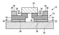
도 1에는 일반적으로 10으로 표시된 전기 디바이스의 장착 및 접속을 위한 장착 조립체가 도시된다. 장착 조립체는 2개의 금속 층(14, 16)에 의해 또는 2개의 금속 판(14, 16)에 의해 형성되는 리드 프레임(12)을 포함한다. 금속 층(14, 16)은 상부 접촉 영역 또는 상부 접촉 패드에 의해 전기 디바이스(22)의 접촉 패드(18, 20)에 전기적으로 접속된다. 접촉 패드(18, 20)는 땜납과 같은 접속 재료(26)에 의해 리드 프레임(12) 또는 금속 층(14, 16)의 상부 표면(24)에 층류 접속된다. 리드 프레임(12) 또는 금속 층(14, 16)은 일반적으로 장착 조립체(10)의 장착을 위한 또한 장착 조립체(10)의 전기적 접속을 위한 인쇄 회로 기판(34)의 접촉 패드(30, 32)에 하부 접촉 영역 또는 하부 접촉 패드에 의해서 접속되는 하부 표면(28)을 갖는다. 하부 표면(28)은 땜납과 같은 접속 재료(36)에 의해 접촉 패드(30, 32)에 층류 접속된다. 유전체 층(38)은 리드 프레임(12)의 상부 표면(24)에 접속되어, 전기 디바이스(22)를 둘러싸고/둘러싸거나 전기 디바이스(22)를 적어도 부분적으로 수납(receive)한다. 유전체 층(38)은 입사 광을 반사시키기 위한 반사 층을 포함하는 상부 표면(40)을 갖는다. 유전체 층(38)은 전기 디바이스(22)를 위한 공동부(cavity)를 형성한다. 전기 디바이스(22)는 바람직하게는 광을 방출하기 위한 발광 다이오드(22)이다.1 shows a mounting assembly for mounting and connecting an electrical device, indicated generally at 10 . The mounting assembly includes a
전기 디바이스(22)의 접촉 패드(18, 20)가 하부 접촉부로서 형성되어 리드 프레임(12)의 상부 표면(24)에 층류 접속되므로, 이 접속에 의해 양호한 열적 접촉이 형성되어 전기 디바이스(22)로부터 리드 프레임(12)의 금속 층(14, 16)으로 열적 전력(thermal power)이 소산될 수 있게 된다. 리드 프레임(12)의 금속 층(14, 16)이 인쇄 회로 기판(34)의 접촉 패드(30, 32)에 층류 접속되므로, 금속 층(14, 16)을 통해 인쇄 회로 기판(34)으로 열 에너지가 소산될 수 있어, 전반적인 전력 소산이 향상될 수 있게 된다. 따라서, 전기 디바이스(22)의 치수가 감소될 수 있으며, 전기적 성능이 일정하게 유지될 수 있다.Since the
도 1에 도시된 바와 같은 리드 프레임(12)은 전기 디바이스(22)의 전기적 접속을 위해 또한 전기 디바이스(22)로부터 소산되는 전력에 대한 히트 싱크(heat sink)를 제공하기 위해 한 평면에 배치된 2개의 금속 층(14, 16)을 포함하는 패턴 리드 프레임으로서 형성된다. 패턴 리드 프레임(12)은 전기 디바이스(22)를 위한 복수의 독립적인 전기 접속을 제공하기 위해 2개의 금속 층(14, 16)보다 많은 금속 층을 포함할 수도 있음을 알아야 할 것이다.The
금속 층(14)과 금속 층(16)은 거리 또는 갭에 의해 분리되어 금속 층(14)과 금속 층(16) 사이에 전기적 격리를 제공한다. 이러한 특정 실시형태에서, 금속 층(14, 16)은 견부(shoulder)(42) 또는 단차부(step)(42)를 갖는다. 견부(42) 또는 단차부(42)에 의해서, 상부 표면(24)에서의 금속 층(14)과 금속 층(16) 사이의 거리는 하부 표면(28)에서의 금속 층(14)과 금속 층(16) 사이의 거리보다 작다. 이들 상이한 거리에 의해, 전기 디바이스(22)의 접촉 패드들(18, 20) 및 인쇄 회로 기판(34)의 접촉 패드들(30, 32)의 상이한 피치가 서로 적응될 수 있다.
도 2는 도 1의 장착 조립체(10)에 대한 분해도이다. 동일한 요소는 동일한 참조 번호로 표시되고, 여기서는 단지 차이점에 대해서만 상세히 설명한다.FIG. 2 is an exploded view of the mounting
금속 층(14, 16)은 금속 층(14, 16)의 반대 측에 서로 평행하게 형성되는 상부 표면(24)과 하부 표면(28)을 갖는다. 전기 디바이스(22)의 접촉 패드(18, 20)는 접촉 패드(18, 20)를 리드 프레임(12)에 전기적 및 열적으로 접속하기 위하여 접속 재료(26)에 의해 각 금속 층(14, 16)의 상부 표면(24)에 층류 접속된다. 금속 층(14, 16)의 하부 표면(28)은 금속 층(14, 16)이 인쇄 회로 기판(34)에 전기적 및 열적으로 접속되도록 접속 재료(36)에 의해 인쇄 회로 기판의 접속 패드(30, 32)에 층류 접속된다. 따라서, 전기 디바이스(22)의 전력 소산이 향상될 수 있는데, 그 이유는 접촉 패드(18, 20)를 열적 전력 소산을 위해 전기 디바이스(22)를 전기적으로 접속시키는데 사용해서 전기 디바이스(22)의 열적 전력이 소산될 수 있도록 하고 전기 디바이스(22)의 향상된 냉각이 실현될 수 있도록 하기 때문이다.The metal layers 14 , 16 have an
도 3a는 장착 조립체(10)의 실시형태를 도시한 것이다. 동일한 요소는 동일한 참조 번호로 표시되고, 여기서는 단지 차이점에 대해서만 상세히 설명한다.3A shows an embodiment of a mounting
리드 프레임(12)은 한 평면 내에 배치되는 2개의 금속 층(14, 16)을 포함하고, 여기서 금속 층(14)과 금속 층(16) 간의 거리(d)는 상부 표면(24) 및 하부 표면(28)에서 동일하다. 상부 표면(24)에는 유전체 층(38)이 접속되어, 전기 디바이스(22)가 배치되는 공동부(44)를 형성한다. 거리(d)는 전기 디바이스(22)의 접촉 패드들(18, 20) 및 인쇄 회로 기판(34)의 접촉 패드들(30, 32) 간의 피치를 형성하고, 피치가 동일한 전기 디바이스(22) 및 인쇄 회로 기판(34)에 대해 이 리드 프레임(12)을 사용할 수 있다.The
도 3b는 장착 조립체(10)의 다른 실시형태를 도시한 것이다. 동일한 요소는 동일한 참조 번호로 표시되고, 여기서는 단지 차이점에 대해서만 상세히 설명한다.3B shows another embodiment of the mounting
한 평면 내에 배치되는 금속 층(14, 16)은 견부(42) 또는 단차부(42)를 포함하여, 금속 층들(14, 16)의 상부 표면들(24)이 제1 거리(d1)로 배치되도록 하고 금속 층들(14, 16)의 하부 표면들(28)이 제2 거리(d2)로 배치되도록 한다. 제1 거리(d1)를 제2 거리(d2)보다 작게 함으로써, (도 3b에는 도시하지 않은) 인쇄 회로 기판(34)의 접촉 패드(30, 32)의 큰 피치가 전기 디바이스(22)의 접촉 패드(18, 20)의 작은 피치에 대해 적응될 수 있다.The
제2 리드 프레임(46)을 유전체 층(38)의 상부 표면(40)에 접속시켜 일반적으로 장착 조립체(10)의 기계적 강화를 제공하고, 여기서는 리드 프레임(46)의 상부 표면(48)에 장착 조립체(10)의 반사 기능을 제공한다. 따라서, 적은 기술적 노력으로도 장착 조립체(10)의 기계적 안정성이 제공되고, 장착 조립체(10)의 반사 기능은 상부 표면(48)에 의해서 제공된다. 리드 프레임(46)은 전기 디바이스(22)를 수납하기 위한 공동부(44)가 형성될 수 있도록 유전체 층(38)의 리세스(recess)와 동일하거나 유전체 층(38)의 리세스보다 큰 리세스 또는 개구부(opening)를 포함한다.A
도 4에는, 장착 조립체(10)와 전기 디바이스(22)의 투시도가 개략적으로 도시된다. 동일한 요소는 동일한 참조 번호로 표시되고, 여기서는 단지 차이점에 대해서만 상세히 설명한다.4 schematically shows a perspective view of the mounting
금속 층(14, 16)은 전기 디바이스(22)에 의해 소산되는 열을 받아서 전도시키기 위한 금속 판(14, 16)으로서, 특히, 구리 판(14, 16)으로서 형성된다. 금속 판(14, 16)은 한 평면 내에 나란히 배치된다. 유전체 층(38)은 금속 층(14, 16)의 상부 표면(24)에 층류 접속되어, 전기 디바이스(22)가 배치되는 공동부(44)를 형성한다. 유전체 층(38)은 바람직하게는 유리 강화 에폭시 층(glass reinforced epoxy layer) 또는 폴리이미드 유전체 층(polyimide dielectric layer)에 의해 형성되며, 여기서 상부 표면(40)은 일반적으로 입사 광을 반사시키고 리드 프레임(12)을 보호하기 위해 백색 반사 층 및/또는 보호 층을 포함한다. 금속 층(14, 16)은 전기 디바이스(22)의 전력 소산에서의 피크들(peaks)을 보상하도록 양호한 열 전도성 및 큰 열 용량을 제공하기 위해 바람직하게는 210 내지 300 마이크로미터의 두께를 갖는다. 전기 디바이스(22)는 세라믹 캐리어(54)에 접속되는 LED 유닛(50) 및 TVS 다이오드(52)를 포함하며, 세라믹 캐리어(54)는 공동부(44) 내에 배치되고 금속 층(14, 16)에 접속되어 LED 유닛(50) 및 TVS 다이오드(52)가 리드 프레임(12)에 전기적 및 열적으로 접속되도록 한다.The metal layers 14 , 16 are formed as
도 5a는 장착 조립체(10)의 실시형태에 대한 투시도이다. 동일한 요소는 동일한 참조 번호로 표시되고, 여기서는 단지 차이점에 대해서만 상세히 설명한다.5A is a perspective view of an embodiment of a mounting
장착 조립체(10)는 유전체 층(38)과 구리 층으로 형성되는 리드 프레임(46)을 포함하며, 여기서는 2개의 공동부(44 및 56)가 유전체 층(38) 및 리드 프레임(46) 내에 형성되어 LED(50)와 TSV 다이오드(52)를 수납한다.The mounting
도 5b는 도 5a에 도시된 장착 조립체(10)의 분해도이다. 금속 층들(14, 16)은 거리를 두고 분리되는데, 여기서는 단차부(42)가 금속 층들(14, 16) 각각에 형성되어 금속 층들(14, 16)의 상부 표면들(24)이 제1 거리(d1)만큼 분리되고 하부 표면들(28)이 제2 거리(d2)만큼 분리되도록 한다. 금속 층(14)과 금속 층(16) 사이의 슬릿(slit) 또는 거리 내에는 격리 요소(58)가 배치되어 PCB 기판(34)에 대한 리드 프레임(12)의 접속으로부터 땜납이 금속 층(14)과 금속 층(16) 사이의 갭 내로 흘러 들어가지 못하게 해서 단락 회로가 방지되도록 한다. 격리 요소(58)는 충전(filling) 또는 밀봉(sealing)으로서 형성된다.5B is an exploded view of the mounting
따라서, 기술적 노력 및 비용을 적게 들이고도 상이한 층들을 서로 라미네이트하여 장착 조립체(10)가 제공되도록 할 수 있다.Accordingly, it is possible to provide the mounting
본 발명을 도면에 도시하고 위 설명에서 상세히 설명했으나, 이러한 도시 및 설명은 예시적이고 대표적인 것에 불과하고 제한적인 것은 아니라고 생각되므로, 본 발명이 개시된 실시형태들에 국한되는 것은 아니다. 관련 기술분야의 통상의 기술자라면, 청구 발명을 실시함에 있어서, 개시된 실시형태들에 대한 다른 변형을 도면, 개시내용 및 첨부된 청구범위의 연구를 통해 알 수 있을 것이고 구현할 수 있을 것이다. While the present invention has been shown in the drawings and described in detail in the foregoing description, the present invention is not limited to the disclosed embodiments, as such drawings and descriptions are to be considered illustrative, representative, and not restrictive. Other modifications to the disclosed embodiments will become apparent to and able to be realized by those skilled in the art through a study of the drawings, the disclosure, and the appended claims, in practicing the claimed invention.
청구 범위에서, "포함하는"이란 단어는 다른 요소들 또는 단계들을 배제하는 것이 아니며, 단수 표현은 복수 표현을 배제하는 것이 아니다. 단일 요소 또는 다른 유닛이 청구범위에 기재된 여러 항목의 기능들을 충족시킬 수도 있다. 특정 수단을 서로 다른 종속항에 기재했다는 사실만으로, 그들 수단을 조합하여 유리하게 사용할 수 없다고 해석해서는 안 된다.In the claims, the word "comprising" does not exclude other elements or steps, and the singular does not exclude the plural. A single element or other unit may fulfill the functions of several items recited in the claims. The mere fact that certain measures are recited in different dependent claims should not be construed as not being able to use them advantageously in combination.
청구범위의 어떠한 참조 부호도 범위를 제한하는 것으로 해석되어서는 안 된다.Any reference signs in the claims should not be construed as limiting the scope.
Claims (14)
Translated fromKorean각각 상부 표면(24)과 하부 표면(28)을 갖는 적어도 2개의 금속 층(14, 16)을 포함하는 장착 요소(mounting element)(12)와,
상기 발광 다이오드에 대한 평면형 전기적 및 열적 접촉(planar electrical and thermal contact)을 제공하기 위한 상기 금속 층들 각각의 상부 표면에 있는 상부 접촉 영역(top contact area) 또는 상부 접촉 패드(top contact pad)
를 포함하며,
상기 금속 층들 각각의 하부 표면에 형성되는 하부 접촉 영역(bottom contact area) 또는 하부 접촉 패드(bottom contact pad) - 상기 금속 층들은 상기 금속 층들 사이에 서로 다른 거리(d1, d2)를 형성하는 2개의 거리 부분을 포함하며, 상기 상부 표면들의 거리(d2)는 상기 하부 표면들의 거리보다 작음 - 와,
장착 기판(34)
을 더 포함하며, 상기 장착 요소의 상기 하부 접촉 영역 또는 상기 하부 접촉 패드는 상기 장착 기판에 전기적 및 열적으로 접속되고,
상기 상부 접촉 영역 또는 상부 접촉 패드와 상기 하부 접촉 영역 또는 하부 접촉 패드는 상기 상부 표면 상에서 수직 관측 방향(vertical viewing direction)에서 제각기 중첩되는 장착 조립체.A mounting assembly (10) for mounting and connecting a light emitting diode, comprising:
a mounting element (12) comprising at least two metal layers (14, 16) each having an upper surface (24) and a lower surface (28);
a top contact area or top contact pad on the top surface of each of the metal layers to provide planar electrical and thermal contact to the light emitting diode
includes,
a bottom contact area or bottom contact pad formed on the lower surface of each of the metal layers - the metal layers forming two different distances d1 and d2 between the metal layers a distance portion, wherein the distance d2 of the upper surfaces is less than the distance of the lower surfaces;
Mounting Board (34)
wherein the lower contact region or the lower contact pad of the mounting element is electrically and thermally connected to the mounting substrate;
and the upper contact area or upper contact pad and the lower contact area or lower contact pad respectively overlap in a vertical viewing direction on the upper surface.
Applications Claiming Priority (3)
| Application Number | Priority Date | Filing Date | Title |
|---|---|---|---|
| EP13196006.4 | 2013-12-06 | ||
| EP13196006 | 2013-12-06 | ||
| PCT/EP2014/075349WO2015082237A1 (en) | 2013-12-06 | 2014-11-24 | Mounting assembly and lighting device |
Publications (2)
| Publication Number | Publication Date |
|---|---|
| KR20160096136A KR20160096136A (en) | 2016-08-12 |
| KR102282209B1true KR102282209B1 (en) | 2021-07-28 |
Family
ID=49759064
Family Applications (1)
| Application Number | Title | Priority Date | Filing Date |
|---|---|---|---|
| KR1020167017963AActiveKR102282209B1 (en) | 2013-12-06 | 2014-11-24 | Mounting assembly and lighting device |
Country Status (6)
| Country | Link |
|---|---|
| US (1) | US10236429B2 (en) |
| EP (1) | EP3078063B1 (en) |
| JP (1) | JP6522615B2 (en) |
| KR (1) | KR102282209B1 (en) |
| CN (1) | CN105993081A (en) |
| WO (1) | WO2015082237A1 (en) |
Families Citing this family (6)
| Publication number | Priority date | Publication date | Assignee | Title |
|---|---|---|---|---|
| GB201318911D0 (en)* | 2013-10-25 | 2013-12-11 | Litecool Ltd | LED Package |
| DE102014212455B4 (en)* | 2014-06-27 | 2024-07-04 | Robert Bosch Gmbh | Diode with a plate-shaped semiconductor element |
| TWI820026B (en)* | 2017-06-21 | 2023-11-01 | 荷蘭商露明控股公司 | Lighting assembly with improved thermal behaviour |
| DE102018123031A1 (en)* | 2018-09-19 | 2020-03-19 | Osram Opto Semiconductors Gmbh | COMPONENT AND MANUFACTURING METHOD FOR A COMPONENT |
| US11252821B2 (en)* | 2019-08-13 | 2022-02-15 | CoreLed Systems, LLC | Optical surface-mount devices |
| DE102021110089A1 (en)* | 2021-04-21 | 2022-10-27 | OSRAM Opto Semiconductors Gesellschaft mit beschränkter Haftung | METHOD OF MANUFACTURING A CAVITY COMPONENT AND A CAVITY COMPONENT |
Citations (2)
| Publication number | Priority date | Publication date | Assignee | Title |
|---|---|---|---|---|
| JP2010021374A (en)* | 2008-07-10 | 2010-01-28 | Hitachi Cable Ltd | Semiconductor package |
| JP2010212352A (en)* | 2009-03-09 | 2010-09-24 | Sanyo Electric Co Ltd | Substrate for light-emitting device, light-emitting device, method of manufacturing those, and light-emitting module |
Family Cites Families (16)
| Publication number | Priority date | Publication date | Assignee | Title |
|---|---|---|---|---|
| JP3991624B2 (en)* | 2001-06-26 | 2007-10-17 | 日亜化学工業株式会社 | Surface mount type light emitting device and manufacturing method thereof |
| TW567619B (en)* | 2001-08-09 | 2003-12-21 | Matsushita Electric Industrial Co Ltd | LED lighting apparatus and card-type LED light source |
| JP3910171B2 (en)* | 2003-02-18 | 2007-04-25 | シャープ株式会社 | Semiconductor light emitting device, method for manufacturing the same, and electronic imaging device |
| TW594950B (en)* | 2003-03-18 | 2004-06-21 | United Epitaxy Co Ltd | Light emitting diode and package scheme and method thereof |
| TWI269423B (en)* | 2005-02-02 | 2006-12-21 | Phoenix Prec Technology Corp | Substrate assembly with direct electrical connection as a semiconductor package |
| JP2007194525A (en)* | 2006-01-23 | 2007-08-02 | Matsushita Electric Ind Co Ltd | Semiconductor light emitting device |
| KR101488448B1 (en)* | 2007-12-06 | 2015-02-02 | 서울반도체 주식회사 | LED package and manufacturing method thereof |
| KR20110008550A (en)* | 2009-07-20 | 2011-01-27 | 삼성전자주식회사 | Light emitting element and manufacturing method thereof |
| JP2011108998A (en) | 2009-11-20 | 2011-06-02 | Toppan Printing Co Ltd | Lead frame for led light emitting element |
| JP2011187552A (en)* | 2010-03-05 | 2011-09-22 | Citizen Electronics Co Ltd | Light-emitting device |
| CN102804428B (en)* | 2010-03-30 | 2016-09-21 | 大日本印刷株式会社 | Lead frame or substrate for LED, semiconductor device, and method for manufacturing lead frame or substrate for LED |
| JP2013033909A (en) | 2011-06-29 | 2013-02-14 | Hitachi Cable Ltd | Substrate for mounting light emitting element and led package |
| JP5818149B2 (en) | 2011-09-09 | 2015-11-18 | 大日本印刷株式会社 | Lead frame with resin, semiconductor device, lighting device, method for manufacturing lead frame with resin, and method for manufacturing semiconductor device |
| CN103367619B (en) | 2012-03-30 | 2015-12-02 | 光宝电子(广州)有限公司 | Metal standoff structure and light emitting diode construction |
| CN104335343A (en) | 2012-09-05 | 2015-02-04 | 松下知识产权经营株式会社 | Semiconductor device and method for producing same |
| KR101997247B1 (en)* | 2012-11-14 | 2019-07-08 | 엘지이노텍 주식회사 | Light emitting device and light apparatus having thereof |
- 2014
- 2014-11-24USUS15/101,322patent/US10236429B2/enactiveActive
- 2014-11-24WOPCT/EP2014/075349patent/WO2015082237A1/enactiveApplication Filing
- 2014-11-24JPJP2016535644Apatent/JP6522615B2/enactiveActive
- 2014-11-24CNCN201480066642.XApatent/CN105993081A/enactivePending
- 2014-11-24KRKR1020167017963Apatent/KR102282209B1/enactiveActive
- 2014-11-24EPEP14802868.1Apatent/EP3078063B1/enactiveActive
Patent Citations (2)
| Publication number | Priority date | Publication date | Assignee | Title |
|---|---|---|---|---|
| JP2010021374A (en)* | 2008-07-10 | 2010-01-28 | Hitachi Cable Ltd | Semiconductor package |
| JP2010212352A (en)* | 2009-03-09 | 2010-09-24 | Sanyo Electric Co Ltd | Substrate for light-emitting device, light-emitting device, method of manufacturing those, and light-emitting module |
Also Published As
| Publication number | Publication date |
|---|---|
| JP6522615B2 (en) | 2019-05-29 |
| US20160315240A1 (en) | 2016-10-27 |
| JP2016539508A (en) | 2016-12-15 |
| KR20160096136A (en) | 2016-08-12 |
| US10236429B2 (en) | 2019-03-19 |
| CN105993081A (en) | 2016-10-05 |
| WO2015082237A1 (en) | 2015-06-11 |
| EP3078063A1 (en) | 2016-10-12 |
| EP3078063B1 (en) | 2020-06-10 |
Similar Documents
| Publication | Publication Date | Title |
|---|---|---|
| KR102282209B1 (en) | Mounting assembly and lighting device | |
| KR101934075B1 (en) | Film system for led applications | |
| US9945526B2 (en) | Optoelectronic lighting module, optoelectronic lighting apparatus and vehicle headlamp | |
| KR100752239B1 (en) | Power module package structure | |
| JP2005158957A (en) | Light emitting device | |
| KR100990331B1 (en) | Heat dissipation structure of high power led using fr4 pcb | |
| JP5288642B2 (en) | Light emitting element | |
| KR20150015900A (en) | Led chip-on-board type rigid flexible pcb and rigid flexible heat spreader sheet pad and heat-sink structure using the same | |
| JP2008130823A (en) | Lighting device, and electronic equipment with it | |
| JP2018139317A (en) | Component carrier and component carrier assembly | |
| US20100301359A1 (en) | Light Emitting Diode Package Structure | |
| US20090010011A1 (en) | Solid state lighting device with heat-dissipating capability | |
| TWI809017B (en) | Photoelectric Hybrid Substrate | |
| TW201407748A (en) | LED light bar | |
| JP2009147258A (en) | LED package and light emitting module | |
| KR101824734B1 (en) | Light emitting module | |
| KR101237685B1 (en) | Heat radiating substrate and method of manufacturing the same | |
| KR102203683B1 (en) | Printed circuit board and luminous device including the same | |
| KR101963738B1 (en) | Led lighting apparatus | |
| KR101259876B1 (en) | Led package having a thermoelectric element and method for manufacturin thereof | |
| KR200452491Y1 (en) | LED printed circuit board with excellent heat dissipation | |
| JP2012253073A (en) | Semiconductor device | |
| KR101064013B1 (en) | Light emitting module | |
| CN109699115B (en) | Optical module | |
| JP2013004824A (en) | Led lighting device and method for manufacturing led lighting device |
Legal Events
| Date | Code | Title | Description |
|---|---|---|---|
| PA0105 | International application | St.27 status event code:A-0-1-A10-A15-nap-PA0105 | |
| E13-X000 | Pre-grant limitation requested | St.27 status event code:A-2-3-E10-E13-lim-X000 | |
| P11-X000 | Amendment of application requested | St.27 status event code:A-2-2-P10-P11-nap-X000 | |
| P13-X000 | Application amended | St.27 status event code:A-2-2-P10-P13-nap-X000 | |
| PG1501 | Laying open of application | St.27 status event code:A-1-1-Q10-Q12-nap-PG1501 | |
| PN2301 | Change of applicant | St.27 status event code:A-3-3-R10-R13-asn-PN2301 St.27 status event code:A-3-3-R10-R11-asn-PN2301 | |
| A201 | Request for examination | ||
| PA0201 | Request for examination | St.27 status event code:A-1-2-D10-D11-exm-PA0201 | |
| E902 | Notification of reason for refusal | ||
| PE0902 | Notice of grounds for rejection | St.27 status event code:A-1-2-D10-D21-exm-PE0902 | |
| E13-X000 | Pre-grant limitation requested | St.27 status event code:A-2-3-E10-E13-lim-X000 | |
| P11-X000 | Amendment of application requested | St.27 status event code:A-2-2-P10-P11-nap-X000 | |
| P13-X000 | Application amended | St.27 status event code:A-2-2-P10-P13-nap-X000 | |
| E701 | Decision to grant or registration of patent right | ||
| PE0701 | Decision of registration | St.27 status event code:A-1-2-D10-D22-exm-PE0701 | |
| GRNT | Written decision to grant | ||
| PR0701 | Registration of establishment | St.27 status event code:A-2-4-F10-F11-exm-PR0701 | |
| PR1002 | Payment of registration fee | St.27 status event code:A-2-2-U10-U12-oth-PR1002 Fee payment year number:1 | |
| PG1601 | Publication of registration | St.27 status event code:A-4-4-Q10-Q13-nap-PG1601 | |
| PR1001 | Payment of annual fee | St.27 status event code:A-4-4-U10-U11-oth-PR1001 Fee payment year number:4 | |
| P22-X000 | Classification modified | St.27 status event code:A-4-4-P10-P22-nap-X000 | |
| PR1001 | Payment of annual fee | St.27 status event code:A-4-4-U10-U11-oth-PR1001 Fee payment year number:5 |