KR102281727B1 - Holding circuit and semiconductor device including the holding circuit - Google Patents
Holding circuit and semiconductor device including the holding circuitDownload PDFInfo
- Publication number
- KR102281727B1 KR102281727B1KR1020167026857AKR20167026857AKR102281727B1KR 102281727 B1KR102281727 B1KR 102281727B1KR 1020167026857 AKR1020167026857 AKR 1020167026857AKR 20167026857 AKR20167026857 AKR 20167026857AKR 102281727 B1KR102281727 B1KR 102281727B1
- Authority
- KR
- South Korea
- Prior art keywords
- circuit
- transistor
- terminal
- oxide
- layer
- Prior art date
- Legal status (The legal status is an assumption and is not a legal conclusion. Google has not performed a legal analysis and makes no representation as to the accuracy of the status listed.)
- Active
Links
- 239000004065semiconductorSubstances0.000titleclaimsabstractdescription252
- 239000003990capacitorSubstances0.000claimsabstractdescription32
- 230000008859changeEffects0.000abstractdescription7
- 238000007667floatingMethods0.000abstractdescription7
- 238000003860storageMethods0.000abstractdescription5
- 239000010410layerSubstances0.000description192
- 239000010408filmSubstances0.000description129
- 238000000034methodMethods0.000description55
- 239000000758substrateSubstances0.000description55
- 239000013078crystalSubstances0.000description52
- 230000006870functionEffects0.000description52
- 239000011701zincSubstances0.000description43
- 239000007789gasSubstances0.000description41
- 229910052760oxygenInorganic materials0.000description26
- 239000012535impuritySubstances0.000description25
- QVGXLLKOCUKJST-UHFFFAOYSA-Natomic oxygenChemical compound[O]QVGXLLKOCUKJST-UHFFFAOYSA-N0.000description24
- 239000001301oxygenSubstances0.000description24
- 125000004429atomChemical group0.000description23
- XUIMIQQOPSSXEZ-UHFFFAOYSA-NSiliconChemical compound[Si]XUIMIQQOPSSXEZ-UHFFFAOYSA-N0.000description20
- 229910052739hydrogenInorganic materials0.000description20
- 239000001257hydrogenSubstances0.000description20
- 229910052751metalInorganic materials0.000description20
- 229910052710siliconInorganic materials0.000description20
- 239000010703siliconSubstances0.000description19
- 238000010586diagramMethods0.000description15
- 238000012545processingMethods0.000description15
- 230000008569processEffects0.000description14
- 230000000694effectsEffects0.000description12
- TWNQGVIAIRXVLR-UHFFFAOYSA-Noxo(oxoalumanyloxy)alumaneChemical compoundO=[Al]O[Al]=OTWNQGVIAIRXVLR-UHFFFAOYSA-N0.000description12
- 238000000151depositionMethods0.000description11
- 230000008021depositionEffects0.000description11
- 229910000449hafnium oxideInorganic materials0.000description11
- WIHZLLGSGQNAGK-UHFFFAOYSA-Nhafnium(4+);oxygen(2-)Chemical compound[O-2].[O-2].[Hf+4]WIHZLLGSGQNAGK-UHFFFAOYSA-N0.000description11
- 238000004519manufacturing processMethods0.000description11
- 239000002184metalSubstances0.000description11
- UFHFLCQGNIYNRP-UHFFFAOYSA-NHydrogenChemical compound[H][H]UFHFLCQGNIYNRP-UHFFFAOYSA-N0.000description10
- 229910052581Si3N4Inorganic materials0.000description10
- 229910052782aluminiumInorganic materials0.000description10
- 238000002173high-resolution transmission electron microscopyMethods0.000description10
- 150000002431hydrogenChemical class0.000description10
- PLDDOISOJJCEMH-UHFFFAOYSA-Nneodymium(3+);oxygen(2-)Chemical compound[O-2].[O-2].[O-2].[Nd+3].[Nd+3]PLDDOISOJJCEMH-UHFFFAOYSA-N0.000description10
- VYPSYNLAJGMNEJ-UHFFFAOYSA-Nsilicon dioxideInorganic materialsO=[Si]=OVYPSYNLAJGMNEJ-UHFFFAOYSA-N0.000description10
- HQVNEWCFYHHQES-UHFFFAOYSA-Nsilicon nitrideChemical compoundN12[Si]34N5[Si]62N3[Si]51N64HQVNEWCFYHHQES-UHFFFAOYSA-N0.000description10
- 238000005477sputtering targetMethods0.000description10
- 229910052721tungstenInorganic materials0.000description9
- 239000010937tungstenSubstances0.000description9
- XKRFYHLGVUSROY-UHFFFAOYSA-NArgonChemical compound[Ar]XKRFYHLGVUSROY-UHFFFAOYSA-N0.000description8
- IJGRMHOSHXDMSA-UHFFFAOYSA-NAtomic nitrogenChemical compoundN#NIJGRMHOSHXDMSA-UHFFFAOYSA-N0.000description8
- 102100030393G-patch domain and KOW motifs-containing proteinHuman genes0.000description8
- XAGFODPZIPBFFR-UHFFFAOYSA-NaluminiumChemical compound[Al]XAGFODPZIPBFFR-UHFFFAOYSA-N0.000description8
- AMWRITDGCCNYAT-UHFFFAOYSA-Lhydroxy(oxo)manganese;manganeseChemical compound[Mn].O[Mn]=O.O[Mn]=OAMWRITDGCCNYAT-UHFFFAOYSA-L0.000description8
- MRELNEQAGSRDBK-UHFFFAOYSA-Nlanthanum(3+);oxygen(2-)Chemical compound[O-2].[O-2].[O-2].[La+3].[La+3]MRELNEQAGSRDBK-UHFFFAOYSA-N0.000description8
- 229910052814silicon oxideInorganic materials0.000description8
- 239000010936titaniumSubstances0.000description8
- WFKWXMTUELFFGS-UHFFFAOYSA-NtungstenChemical compound[W]WFKWXMTUELFFGS-UHFFFAOYSA-N0.000description8
- 229910045601alloyInorganic materials0.000description7
- 239000000956alloySubstances0.000description7
- 238000004458analytical methodMethods0.000description7
- 238000000231atomic layer depositionMethods0.000description7
- 230000007547defectEffects0.000description7
- 238000009792diffusion processMethods0.000description7
- 239000002159nanocrystalSubstances0.000description7
- 229910052719titaniumInorganic materials0.000description7
- 229910017566Cu-MnInorganic materials0.000description6
- 229910017871Cu—MnInorganic materials0.000description6
- 239000010949copperSubstances0.000description6
- AJNVQOSZGJRYEI-UHFFFAOYSA-Ndigallium;oxygen(2-)Chemical compound[O-2].[O-2].[O-2].[Ga+3].[Ga+3]AJNVQOSZGJRYEI-UHFFFAOYSA-N0.000description6
- 229910001195gallium oxideInorganic materials0.000description6
- 239000011261inert gasSubstances0.000description6
- 239000012212insulatorSubstances0.000description6
- SIWVEOZUMHYXCS-UHFFFAOYSA-Noxo(oxoyttriooxy)yttriumChemical compoundO=[Y]O[Y]=OSIWVEOZUMHYXCS-UHFFFAOYSA-N0.000description6
- XLYOFNOQVPJJNP-UHFFFAOYSA-NwaterSubstancesOXLYOFNOQVPJJNP-UHFFFAOYSA-N0.000description6
- 229910001868waterInorganic materials0.000description6
- 229910052727yttriumInorganic materials0.000description6
- OKTJSMMVPCPJKN-UHFFFAOYSA-NCarbonChemical compound[C]OKTJSMMVPCPJKN-UHFFFAOYSA-N0.000description5
- PXHVJJICTQNCMI-UHFFFAOYSA-NNickelChemical compound[Ni]PXHVJJICTQNCMI-UHFFFAOYSA-N0.000description5
- RTAQQCXQSZGOHL-UHFFFAOYSA-NTitaniumChemical compound[Ti]RTAQQCXQSZGOHL-UHFFFAOYSA-N0.000description5
- 230000000903blocking effectEffects0.000description5
- 229910052799carbonInorganic materials0.000description5
- 238000002524electron diffraction dataMethods0.000description5
- 229910052746lanthanumInorganic materials0.000description5
- 239000002356single layerSubstances0.000description5
- 238000004544sputter depositionMethods0.000description5
- 238000002230thermal chemical vapour depositionMethods0.000description5
- 229910052684CeriumInorganic materials0.000description4
- 229910052786argonInorganic materials0.000description4
- 239000002585baseSubstances0.000description4
- PMHQVHHXPFUNSP-UHFFFAOYSA-Mcopper(1+);methylsulfanylmethane;bromideChemical compoundBr[Cu].CSCPMHQVHHXPFUNSP-UHFFFAOYSA-M0.000description4
- 238000010894electron beam technologyMethods0.000description4
- 229910052733galliumInorganic materials0.000description4
- YBMRDBCBODYGJE-UHFFFAOYSA-Ngermanium oxideInorganic materialsO=[Ge]=OYBMRDBCBODYGJE-UHFFFAOYSA-N0.000description4
- 229910052735hafniumInorganic materials0.000description4
- CPLXHLVBOLITMK-UHFFFAOYSA-Nmagnesium oxideInorganic materials[Mg]=OCPLXHLVBOLITMK-UHFFFAOYSA-N0.000description4
- 239000000395magnesium oxideSubstances0.000description4
- AXZKOIWUVFPNLO-UHFFFAOYSA-Nmagnesium;oxygen(2-)Chemical compound[O-2].[Mg+2]AXZKOIWUVFPNLO-UHFFFAOYSA-N0.000description4
- 150000004767nitridesChemical class0.000description4
- 229910052757nitrogenInorganic materials0.000description4
- PVADDRMAFCOOPC-UHFFFAOYSA-NoxogermaniumChemical compound[Ge]=OPVADDRMAFCOOPC-UHFFFAOYSA-N0.000description4
- BPUBBGLMJRNUCC-UHFFFAOYSA-Noxygen(2-);tantalum(5+)Chemical compound[O-2].[O-2].[O-2].[O-2].[O-2].[Ta+5].[Ta+5]BPUBBGLMJRNUCC-UHFFFAOYSA-N0.000description4
- RVTZCBVAJQQJTK-UHFFFAOYSA-Noxygen(2-);zirconium(4+)Chemical compound[O-2].[O-2].[Zr+4]RVTZCBVAJQQJTK-UHFFFAOYSA-N0.000description4
- 239000008188pelletSubstances0.000description4
- 239000011347resinSubstances0.000description4
- 229920005989resinPolymers0.000description4
- 239000000523sampleSubstances0.000description4
- 229910001936tantalum oxideInorganic materials0.000description4
- 229910052718tinInorganic materials0.000description4
- -1tungsten nitrideChemical class0.000description4
- 229910052726zirconiumInorganic materials0.000description4
- 229910001928zirconium oxideInorganic materials0.000description4
- XEEYBQQBJWHFJM-UHFFFAOYSA-NIronChemical compound[Fe]XEEYBQQBJWHFJM-UHFFFAOYSA-N0.000description3
- NRTOMJZYCJJWKI-UHFFFAOYSA-NTitanium nitrideChemical compound[Ti]#NNRTOMJZYCJJWKI-UHFFFAOYSA-N0.000description3
- 238000002441X-ray diffractionMethods0.000description3
- 230000015572biosynthetic processEffects0.000description3
- 230000015556catabolic processEffects0.000description3
- 150000001875compoundsChemical class0.000description3
- 239000004020conductorSubstances0.000description3
- HQWPLXHWEZZGKY-UHFFFAOYSA-NdiethylzincChemical compoundCC[Zn]CCHQWPLXHWEZZGKY-UHFFFAOYSA-N0.000description3
- 229910052732germaniumInorganic materials0.000description3
- VBJZVLUMGGDVMO-UHFFFAOYSA-Nhafnium atomChemical compound[Hf]VBJZVLUMGGDVMO-UHFFFAOYSA-N0.000description3
- 125000005843halogen groupChemical group0.000description3
- AMGQUBHHOARCQH-UHFFFAOYSA-Nindium;oxotinChemical compound[In].[Sn]=OAMGQUBHHOARCQH-UHFFFAOYSA-N0.000description3
- 238000009413insulationMethods0.000description3
- 238000003475laminationMethods0.000description3
- 239000000463materialSubstances0.000description3
- 229910021421monocrystalline siliconInorganic materials0.000description3
- 230000000737periodic effectEffects0.000description3
- 230000002093peripheral effectEffects0.000description3
- 238000011084recoveryMethods0.000description3
- 239000010409thin filmSubstances0.000description3
- 229910052725zincInorganic materials0.000description3
- CURLTUGMZLYLDI-UHFFFAOYSA-NCarbon dioxideChemical compoundO=C=OCURLTUGMZLYLDI-UHFFFAOYSA-N0.000description2
- MYMOFIZGZYHOMD-UHFFFAOYSA-NDioxygenChemical compoundO=OMYMOFIZGZYHOMD-UHFFFAOYSA-N0.000description2
- GYHNNYVSQQEPJS-UHFFFAOYSA-NGalliumChemical compound[Ga]GYHNNYVSQQEPJS-UHFFFAOYSA-N0.000description2
- 229910052779NeodymiumInorganic materials0.000description2
- BQCADISMDOOEFD-UHFFFAOYSA-NSilverChemical compound[Ag]BQCADISMDOOEFD-UHFFFAOYSA-N0.000description2
- 238000003917TEM imageMethods0.000description2
- GWEVSGVZZGPLCZ-UHFFFAOYSA-NTitan oxideChemical compoundO=[Ti]=OGWEVSGVZZGPLCZ-UHFFFAOYSA-N0.000description2
- 229910007541Zn OInorganic materials0.000description2
- 229910052783alkali metalInorganic materials0.000description2
- 150000001340alkali metalsChemical class0.000description2
- 229910052784alkaline earth metalInorganic materials0.000description2
- 150000001342alkaline earth metalsChemical class0.000description2
- 230000005540biological transmissionEffects0.000description2
- 239000011651chromiumSubstances0.000description2
- 238000004891communicationMethods0.000description2
- 239000000470constituentSubstances0.000description2
- 238000002425crystallisationMethods0.000description2
- 230000008025crystallizationEffects0.000description2
- 229910001882dioxygenInorganic materials0.000description2
- 230000005684electric fieldEffects0.000description2
- 238000005516engineering processMethods0.000description2
- 239000003822epoxy resinSubstances0.000description2
- 230000005669field effectEffects0.000description2
- 239000011888foilSubstances0.000description2
- 239000011521glassSubstances0.000description2
- PCHJSUWPFVWCPO-UHFFFAOYSA-NgoldChemical compound[Au]PCHJSUWPFVWCPO-UHFFFAOYSA-N0.000description2
- 239000010931goldSubstances0.000description2
- 229910052738indiumInorganic materials0.000description2
- APFVFJFRJDLVQX-UHFFFAOYSA-Nindium atomChemical compound[In]APFVFJFRJDLVQX-UHFFFAOYSA-N0.000description2
- 229910003437indium oxideInorganic materials0.000description2
- PJXISJQVUVHSOJ-UHFFFAOYSA-Nindium(iii) oxideChemical compound[O-2].[O-2].[O-2].[In+3].[In+3]PJXISJQVUVHSOJ-UHFFFAOYSA-N0.000description2
- 239000011572manganeseSubstances0.000description2
- 239000000203mixtureSubstances0.000description2
- 238000000465mouldingMethods0.000description2
- 229910052759nickelInorganic materials0.000description2
- QGLKJKCYBOYXKC-UHFFFAOYSA-NnonaoxidotritungstenChemical compoundO=[W]1(=O)O[W](=O)(=O)O[W](=O)(=O)O1QGLKJKCYBOYXKC-UHFFFAOYSA-N0.000description2
- 230000035515penetrationEffects0.000description2
- 239000004033plasticSubstances0.000description2
- 229920003023plasticPolymers0.000description2
- 238000007747platingMethods0.000description2
- 229920000647polyepoxidePolymers0.000description2
- 229920000728polyesterPolymers0.000description2
- 229920000139polyethylene terephthalatePolymers0.000description2
- 239000005020polyethylene terephthalateSubstances0.000description2
- 229920001721polyimidePolymers0.000description2
- 238000012805post-processingMethods0.000description2
- 230000001681protective effectEffects0.000description2
- 239000010453quartzSubstances0.000description2
- 239000002994raw materialSubstances0.000description2
- 239000010935stainless steelSubstances0.000description2
- 229910001220stainless steelInorganic materials0.000description2
- 239000000126substanceSubstances0.000description2
- 238000012360testing methodMethods0.000description2
- OGIDPMRJRNCKJF-UHFFFAOYSA-Ntitanium oxideInorganic materials[Ti]=OOGIDPMRJRNCKJF-UHFFFAOYSA-N0.000description2
- XCZXGTMEAKBVPV-UHFFFAOYSA-NtrimethylgalliumChemical compoundC[Ga](C)CXCZXGTMEAKBVPV-UHFFFAOYSA-N0.000description2
- IBEFSUTVZWZJEL-UHFFFAOYSA-NtrimethylindiumChemical compoundC[In](C)CIBEFSUTVZWZJEL-UHFFFAOYSA-N0.000description2
- 229910001930tungsten oxideInorganic materials0.000description2
- 238000004402ultra-violet photoelectron spectroscopyMethods0.000description2
- 229910001233yttria-stabilized zirconiaInorganic materials0.000description2
- VWQVUPCCIRVNHF-UHFFFAOYSA-Nyttrium atomChemical compound[Y]VWQVUPCCIRVNHF-UHFFFAOYSA-N0.000description2
- YVTHLONGBIQYBO-UHFFFAOYSA-Nzinc indium(3+) oxygen(2-)Chemical compound[O--].[Zn++].[In+3]YVTHLONGBIQYBO-UHFFFAOYSA-N0.000description2
- 239000004925Acrylic resinSubstances0.000description1
- 229920000178Acrylic resinPolymers0.000description1
- ZOXJGFHDIHLPTG-UHFFFAOYSA-NBoronChemical compound[B]ZOXJGFHDIHLPTG-UHFFFAOYSA-N0.000description1
- VYZAMTAEIAYCRO-UHFFFAOYSA-NChromiumChemical compound[Cr]VYZAMTAEIAYCRO-UHFFFAOYSA-N0.000description1
- RYGMFSIKBFXOCR-UHFFFAOYSA-NCopperChemical compound[Cu]RYGMFSIKBFXOCR-UHFFFAOYSA-N0.000description1
- 239000004593EpoxySubstances0.000description1
- 229910001111Fine metalInorganic materials0.000description1
- 229910005555GaZnOInorganic materials0.000description1
- PWHULOQIROXLJO-UHFFFAOYSA-NManganeseChemical compound[Mn]PWHULOQIROXLJO-UHFFFAOYSA-N0.000description1
- ZOKXTWBITQBERF-UHFFFAOYSA-NMolybdenumChemical compound[Mo]ZOKXTWBITQBERF-UHFFFAOYSA-N0.000description1
- OAICVXFJPJFONN-UHFFFAOYSA-NPhosphorusChemical compound[P]OAICVXFJPJFONN-UHFFFAOYSA-N0.000description1
- 229920012266Poly(ether sulfone) PESPolymers0.000description1
- 239000004952PolyamideSubstances0.000description1
- 239000004642PolyimideSubstances0.000description1
- 239000004743PolypropyleneSubstances0.000description1
- KJTLSVCANCCWHF-UHFFFAOYSA-NRutheniumChemical compound[Ru]KJTLSVCANCCWHF-UHFFFAOYSA-N0.000description1
- 229910000577Silicon-germaniumInorganic materials0.000description1
- HCHKCACWOHOZIP-UHFFFAOYSA-NZincChemical compound[Zn]HCHKCACWOHOZIP-UHFFFAOYSA-N0.000description1
- 229910007610Zn—SnInorganic materials0.000description1
- LEVVHYCKPQWKOP-UHFFFAOYSA-N[Si].[Ge]Chemical compound[Si].[Ge]LEVVHYCKPQWKOP-UHFFFAOYSA-N0.000description1
- NIXOWILDQLNWCW-UHFFFAOYSA-Nacrylic acid groupChemical groupC(C=C)(=O)ONIXOWILDQLNWCW-UHFFFAOYSA-N0.000description1
- 239000005407aluminoborosilicate glassSubstances0.000description1
- 239000004760aramidSubstances0.000description1
- 229920003235aromatic polyamidePolymers0.000description1
- 229910052785arsenicInorganic materials0.000description1
- RQNWIZPPADIBDY-UHFFFAOYSA-Narsenic atomChemical compound[As]RQNWIZPPADIBDY-UHFFFAOYSA-N0.000description1
- 229910052788bariumInorganic materials0.000description1
- DSAJWYNOEDNPEQ-UHFFFAOYSA-Nbarium atomChemical compound[Ba]DSAJWYNOEDNPEQ-UHFFFAOYSA-N0.000description1
- 238000005452bendingMethods0.000description1
- 230000008901benefitEffects0.000description1
- 229910052796boronInorganic materials0.000description1
- 239000005388borosilicate glassSubstances0.000description1
- 230000005587bubblingEffects0.000description1
- 229910002092carbon dioxideInorganic materials0.000description1
- 239000001569carbon dioxideSubstances0.000description1
- 229910052800carbon group elementInorganic materials0.000description1
- 239000000969carrierSubstances0.000description1
- 239000012159carrier gasSubstances0.000description1
- 238000006243chemical reactionMethods0.000description1
- 238000005229chemical vapour depositionMethods0.000description1
- 229910052804chromiumInorganic materials0.000description1
- 229910017052cobaltInorganic materials0.000description1
- 239000010941cobaltSubstances0.000description1
- GUTLYIVDDKVIGB-UHFFFAOYSA-Ncobalt atomChemical compound[Co]GUTLYIVDDKVIGB-UHFFFAOYSA-N0.000description1
- 239000002131composite materialSubstances0.000description1
- 229910052802copperInorganic materials0.000description1
- 230000008878couplingEffects0.000description1
- 238000010168coupling processMethods0.000description1
- 238000005859coupling reactionMethods0.000description1
- 238000006731degradation reactionMethods0.000description1
- 238000003795desorptionMethods0.000description1
- 230000006866deteriorationEffects0.000description1
- AXAZMDOAUQTMOW-UHFFFAOYSA-NdimethylzincChemical compoundC[Zn]CAXAZMDOAUQTMOW-UHFFFAOYSA-N0.000description1
- KPUWHANPEXNPJT-UHFFFAOYSA-NdisiloxaneChemical class[SiH3]O[SiH3]KPUWHANPEXNPJT-UHFFFAOYSA-N0.000description1
- 239000000428dustSubstances0.000description1
- 210000000883ear externalAnatomy0.000description1
- 238000002003electron diffractionMethods0.000description1
- 238000000605extractionMethods0.000description1
- 239000002657fibrous materialSubstances0.000description1
- 229910052737goldInorganic materials0.000description1
- 229910021480group 4 elementInorganic materials0.000description1
- 229910001385heavy metalInorganic materials0.000description1
- 238000007689inspectionMethods0.000description1
- 239000011810insulating materialSubstances0.000description1
- 239000011229interlayerSubstances0.000description1
- 229910052742ironInorganic materials0.000description1
- 238000002955isolationMethods0.000description1
- FZLIPJUXYLNCLC-UHFFFAOYSA-Nlanthanum atomChemical compound[La]FZLIPJUXYLNCLC-UHFFFAOYSA-N0.000description1
- 239000004973liquid crystal related substanceSubstances0.000description1
- 230000014759maintenance of locationEffects0.000description1
- 229910052748manganeseInorganic materials0.000description1
- 238000002156mixingMethods0.000description1
- 238000012986modificationMethods0.000description1
- 230000004048modificationEffects0.000description1
- 229910052750molybdenumInorganic materials0.000description1
- 239000011733molybdenumSubstances0.000description1
- RUFLMLWJRZAWLJ-UHFFFAOYSA-Nnickel silicideChemical compound[Ni]=[Si]=[Ni]RUFLMLWJRZAWLJ-UHFFFAOYSA-N0.000description1
- 229910021334nickel silicideInorganic materials0.000description1
- QJGQUHMNIGDVPM-UHFFFAOYSA-Nnitrogen groupChemical group[N]QJGQUHMNIGDVPM-UHFFFAOYSA-N0.000description1
- 230000001151other effectEffects0.000description1
- 239000007800oxidant agentSubstances0.000description1
- 125000004430oxygen atomChemical groupO*0.000description1
- 239000005011phenolic resinSubstances0.000description1
- 229910052698phosphorusInorganic materials0.000description1
- 239000011574phosphorusSubstances0.000description1
- 230000000704physical effectEffects0.000description1
- 238000005268plasma chemical vapour depositionMethods0.000description1
- 238000005498polishingMethods0.000description1
- 229920002647polyamidePolymers0.000description1
- 229920006122polyamide resinPolymers0.000description1
- 239000011112polyethylene naphthalateSubstances0.000description1
- 239000009719polyimide resinSubstances0.000description1
- 229920001155polypropylenePolymers0.000description1
- 229920000915polyvinyl chloridePolymers0.000description1
- 239000004800polyvinyl chlorideSubstances0.000description1
- 229920002620polyvinyl fluoridePolymers0.000description1
- 238000007781pre-processingMethods0.000description1
- 238000007639printingMethods0.000description1
- 229910052707rutheniumInorganic materials0.000description1
- 235000015067saucesNutrition0.000description1
- 238000007789sealingMethods0.000description1
- 238000001004secondary ion mass spectrometryMethods0.000description1
- VSZWPYCFIRKVQL-UHFFFAOYSA-Nselanylidenegallium;seleniumChemical compound[Se].[Se]=[Ga].[Se]=[Ga]VSZWPYCFIRKVQL-UHFFFAOYSA-N0.000description1
- HBMJWWWQQXIZIP-UHFFFAOYSA-Nsilicon carbideChemical compound[Si+]#[C-]HBMJWWWQQXIZIP-UHFFFAOYSA-N0.000description1
- 229910010271silicon carbideInorganic materials0.000description1
- 229910052709silverInorganic materials0.000description1
- 239000004332silverSubstances0.000description1
- 239000005361soda-lime glassSubstances0.000description1
- 238000005476solderingMethods0.000description1
- 238000004611spectroscopical analysisMethods0.000description1
- 238000012916structural analysisMethods0.000description1
- 239000000057synthetic resinSubstances0.000description1
- 229920003002synthetic resinPolymers0.000description1
- 229910052715tantalumInorganic materials0.000description1
- GUVRBAGPIYLISA-UHFFFAOYSA-Ntantalum atomChemical compound[Ta]GUVRBAGPIYLISA-UHFFFAOYSA-N0.000description1
- MZLGASXMSKOWSE-UHFFFAOYSA-Ntantalum nitrideChemical compound[Ta]#NMZLGASXMSKOWSE-UHFFFAOYSA-N0.000description1
- JBQYATWDVHIOAR-UHFFFAOYSA-NtellanylidenegermaniumChemical compound[Te]=[Ge]JBQYATWDVHIOAR-UHFFFAOYSA-N0.000description1
- 229910052723transition metalInorganic materials0.000description1
- RGGPNXQUMRMPRA-UHFFFAOYSA-NtriethylgalliumChemical compoundCC[Ga](CC)CCRGGPNXQUMRMPRA-UHFFFAOYSA-N0.000description1
- 238000007740vapor depositionMethods0.000description1
- XLOMVQKBTHCTTD-UHFFFAOYSA-Nzinc oxideInorganic materials[Zn]=OXLOMVQKBTHCTTD-UHFFFAOYSA-N0.000description1
- 239000011787zinc oxideSubstances0.000description1
Images


Classifications
- G—PHYSICS
- G11—INFORMATION STORAGE
- G11C—STATIC STORES
- G11C19/00—Digital stores in which the information is moved stepwise, e.g. shift registers
- G11C19/18—Digital stores in which the information is moved stepwise, e.g. shift registers using capacitors as main elements of the stages
- G11C19/182—Digital stores in which the information is moved stepwise, e.g. shift registers using capacitors as main elements of the stages in combination with semiconductor elements, e.g. bipolar transistors, diodes
- G11C19/184—Digital stores in which the information is moved stepwise, e.g. shift registers using capacitors as main elements of the stages in combination with semiconductor elements, e.g. bipolar transistors, diodes with field-effect transistors, e.g. MOS-FET
- H—ELECTRICITY
- H03—ELECTRONIC CIRCUITRY
- H03K—PULSE TECHNIQUE
- H03K17/00—Electronic switching or gating, i.e. not by contact-making and –breaking
- H03K17/002—Switching arrangements with several input- or output terminals
- H03K17/005—Switching arrangements with several input- or output terminals with several inputs only
- H01L27/1207—
- H01L29/24—
- H—ELECTRICITY
- H03—ELECTRONIC CIRCUITRY
- H03K—PULSE TECHNIQUE
- H03K19/00—Logic circuits, i.e. having at least two inputs acting on one output; Inverting circuits
- H03K19/0008—Arrangements for reducing power consumption
- H03K19/0016—Arrangements for reducing power consumption by using a control or a clock signal, e.g. in order to apply power supply
- H—ELECTRICITY
- H10—SEMICONDUCTOR DEVICES; ELECTRIC SOLID-STATE DEVICES NOT OTHERWISE PROVIDED FOR
- H10D—INORGANIC ELECTRIC SEMICONDUCTOR DEVICES
- H10D30/00—Field-effect transistors [FET]
- H10D30/60—Insulated-gate field-effect transistors [IGFET]
- H10D30/67—Thin-film transistors [TFT]
- H10D30/674—Thin-film transistors [TFT] characterised by the active materials
- H10D30/6755—Oxide semiconductors, e.g. zinc oxide, copper aluminium oxide or cadmium stannate
- H—ELECTRICITY
- H10—SEMICONDUCTOR DEVICES; ELECTRIC SOLID-STATE DEVICES NOT OTHERWISE PROVIDED FOR
- H10D—INORGANIC ELECTRIC SEMICONDUCTOR DEVICES
- H10D30/00—Field-effect transistors [FET]
- H10D30/60—Insulated-gate field-effect transistors [IGFET]
- H10D30/67—Thin-film transistors [TFT]
- H10D30/6757—Thin-film transistors [TFT] characterised by the structure of the channel, e.g. transverse or longitudinal shape or doping profile
- H—ELECTRICITY
- H10—SEMICONDUCTOR DEVICES; ELECTRIC SOLID-STATE DEVICES NOT OTHERWISE PROVIDED FOR
- H10D—INORGANIC ELECTRIC SEMICONDUCTOR DEVICES
- H10D62/00—Semiconductor bodies, or regions thereof, of devices having potential barriers
- H10D62/80—Semiconductor bodies, or regions thereof, of devices having potential barriers characterised by the materials
- H—ELECTRICITY
- H10—SEMICONDUCTOR DEVICES; ELECTRIC SOLID-STATE DEVICES NOT OTHERWISE PROVIDED FOR
- H10D—INORGANIC ELECTRIC SEMICONDUCTOR DEVICES
- H10D86/00—Integrated devices formed in or on insulating or conducting substrates, e.g. formed in silicon-on-insulator [SOI] substrates or on stainless steel or glass substrates
- H10D86/40—Integrated devices formed in or on insulating or conducting substrates, e.g. formed in silicon-on-insulator [SOI] substrates or on stainless steel or glass substrates characterised by multiple TFTs
- H10D86/421—Integrated devices formed in or on insulating or conducting substrates, e.g. formed in silicon-on-insulator [SOI] substrates or on stainless steel or glass substrates characterised by multiple TFTs having a particular composition, shape or crystalline structure of the active layer
- H10D86/423—Integrated devices formed in or on insulating or conducting substrates, e.g. formed in silicon-on-insulator [SOI] substrates or on stainless steel or glass substrates characterised by multiple TFTs having a particular composition, shape or crystalline structure of the active layer comprising semiconductor materials not belonging to the Group IV, e.g. InGaZnO
- H—ELECTRICITY
- H10—SEMICONDUCTOR DEVICES; ELECTRIC SOLID-STATE DEVICES NOT OTHERWISE PROVIDED FOR
- H10D—INORGANIC ELECTRIC SEMICONDUCTOR DEVICES
- H10D86/00—Integrated devices formed in or on insulating or conducting substrates, e.g. formed in silicon-on-insulator [SOI] substrates or on stainless steel or glass substrates
- H10D86/40—Integrated devices formed in or on insulating or conducting substrates, e.g. formed in silicon-on-insulator [SOI] substrates or on stainless steel or glass substrates characterised by multiple TFTs
- H10D86/60—Integrated devices formed in or on insulating or conducting substrates, e.g. formed in silicon-on-insulator [SOI] substrates or on stainless steel or glass substrates characterised by multiple TFTs wherein the TFTs are in active matrices
- H—ELECTRICITY
- H10—SEMICONDUCTOR DEVICES; ELECTRIC SOLID-STATE DEVICES NOT OTHERWISE PROVIDED FOR
- H10D—INORGANIC ELECTRIC SEMICONDUCTOR DEVICES
- H10D87/00—Integrated devices comprising both bulk components and either SOI or SOS components on the same substrate
- G—PHYSICS
- G11—INFORMATION STORAGE
- G11C—STATIC STORES
- G11C11/00—Digital stores characterised by the use of particular electric or magnetic storage elements; Storage elements therefor
- G11C11/21—Digital stores characterised by the use of particular electric or magnetic storage elements; Storage elements therefor using electric elements
- G11C11/24—Digital stores characterised by the use of particular electric or magnetic storage elements; Storage elements therefor using electric elements using capacitors
- G—PHYSICS
- G11—INFORMATION STORAGE
- G11C—STATIC STORES
- G11C11/00—Digital stores characterised by the use of particular electric or magnetic storage elements; Storage elements therefor
- G11C11/21—Digital stores characterised by the use of particular electric or magnetic storage elements; Storage elements therefor using electric elements
- G11C11/34—Digital stores characterised by the use of particular electric or magnetic storage elements; Storage elements therefor using electric elements using semiconductor devices
- G11C11/40—Digital stores characterised by the use of particular electric or magnetic storage elements; Storage elements therefor using electric elements using semiconductor devices using transistors
- G11C11/401—Digital stores characterised by the use of particular electric or magnetic storage elements; Storage elements therefor using electric elements using semiconductor devices using transistors forming cells needing refreshing or charge regeneration, i.e. dynamic cells
- G11C11/403—Digital stores characterised by the use of particular electric or magnetic storage elements; Storage elements therefor using electric elements using semiconductor devices using transistors forming cells needing refreshing or charge regeneration, i.e. dynamic cells with charge regeneration common to a multiplicity of memory cells, i.e. external refresh
- G11C11/405—Digital stores characterised by the use of particular electric or magnetic storage elements; Storage elements therefor using electric elements using semiconductor devices using transistors forming cells needing refreshing or charge regeneration, i.e. dynamic cells with charge regeneration common to a multiplicity of memory cells, i.e. external refresh with three charge-transfer gates, e.g. MOS transistors, per cell
- G—PHYSICS
- G11—INFORMATION STORAGE
- G11C—STATIC STORES
- G11C11/00—Digital stores characterised by the use of particular electric or magnetic storage elements; Storage elements therefor
- G11C11/21—Digital stores characterised by the use of particular electric or magnetic storage elements; Storage elements therefor using electric elements
- G11C11/34—Digital stores characterised by the use of particular electric or magnetic storage elements; Storage elements therefor using electric elements using semiconductor devices
- G11C11/40—Digital stores characterised by the use of particular electric or magnetic storage elements; Storage elements therefor using electric elements using semiconductor devices using transistors
- G11C11/41—Digital stores characterised by the use of particular electric or magnetic storage elements; Storage elements therefor using electric elements using semiconductor devices using transistors forming static cells with positive feedback, i.e. cells not needing refreshing or charge regeneration, e.g. bistable multivibrator or Schmitt trigger
- G11C11/412—Digital stores characterised by the use of particular electric or magnetic storage elements; Storage elements therefor using electric elements using semiconductor devices using transistors forming static cells with positive feedback, i.e. cells not needing refreshing or charge regeneration, e.g. bistable multivibrator or Schmitt trigger using field-effect transistors only
- G—PHYSICS
- G11—INFORMATION STORAGE
- G11C—STATIC STORES
- G11C14/00—Digital stores characterised by arrangements of cells having volatile and non-volatile storage properties for back-up when the power is down
- G11C14/0054—Digital stores characterised by arrangements of cells having volatile and non-volatile storage properties for back-up when the power is down in which the volatile element is a SRAM cell
- G11C14/0063—Digital stores characterised by arrangements of cells having volatile and non-volatile storage properties for back-up when the power is down in which the volatile element is a SRAM cell and the nonvolatile element is an EEPROM element, e.g. a floating gate or MNOS transistor
- H—ELECTRICITY
- H03—ELECTRONIC CIRCUITRY
- H03K—PULSE TECHNIQUE
- H03K3/00—Circuits for generating electric pulses; Monostable, bistable or multistable circuits
- H03K3/02—Generators characterised by the type of circuit or by the means used for producing pulses
- H03K3/353—Generators characterised by the type of circuit or by the means used for producing pulses by the use, as active elements, of field-effect transistors with internal or external positive feedback
- H03K3/356—Bistable circuits
- H03K3/356008—Bistable circuits ensuring a predetermined initial state when the supply voltage has been applied; storing the actual state when the supply voltage fails
Landscapes
- Engineering & Computer Science (AREA)
- Physics & Mathematics (AREA)
- Computer Hardware Design (AREA)
- Computing Systems (AREA)
- General Engineering & Computer Science (AREA)
- Mathematical Physics (AREA)
- Microelectronics & Electronic Packaging (AREA)
- Power Engineering (AREA)
- Thin Film Transistor (AREA)
- Non-Volatile Memory (AREA)
- Electrodes Of Semiconductors (AREA)
- Semiconductor Memories (AREA)
- Static Random-Access Memory (AREA)
- Metal-Oxide And Bipolar Metal-Oxide Semiconductor Integrated Circuits (AREA)
Abstract
Translated fromKoreanDescription
Translated fromKorean본 발명의 일 형태는 상태 또는 데이터를 유지할 수 있는 유지 회로, 순서 회로, 및 기타 반도체 장치, 이의 구동 방법, 및 이의 제작 방법 등에 관한 것이다.One aspect of the present invention relates to a holding circuit, a sequence circuit, and other semiconductor devices capable of holding a state or data, a driving method thereof, a manufacturing method thereof, and the like.
본 발명의 일 형태는 상술한 기술 분야에 한정되지 않는다. 본 명세서, 도면, 및 청구범위(이후에서 "본 명세서 등"이라고 함)에 개시(開示)된 발명의 일 형태의 기술 분야는 물건, 방법, 또는 제작 방법에 관한 것이다. 본 발명의 일 형태는 공정(process), 기계(machine), 제품(manufacture), 또는 조성물(composition of matter)에 관한 것이다. 본 명세서에 개시된 본 발명의 일 형태의 기술 분야의 예는 반도체 장치, 표시 장치, 액정 표시 장치, 발광 장치, 조명 장치, 전력 저장 장치, 기억 장치, 처리 장치, 이들 중 어느 것의 구동 방법, 및 이들 중 어느 것의 제작 방법을 포함한다.One embodiment of the present invention is not limited to the technical field described above. The technical field of one embodiment of the invention disclosed in this specification, drawings, and claims (hereinafter referred to as "this specification and the like") relates to an article, a method, or a manufacturing method. One aspect of the present invention relates to a process, machine, manufacture, or composition of matter. Examples of technical fields of one embodiment of the present invention disclosed herein include semiconductor devices, display devices, liquid crystal display devices, light emitting devices, lighting devices, power storage devices, memory devices, processing devices, driving methods of any of these, and these a method of making any of them.
반도체 장치의 소비 전력을 저감하기 위하여, 불필요한 회로의 동작을 파워 게이팅 또는 클럭 게이팅에 의하여 정지한다. 플립플롭 회로(FF)는 반도체 장치에 많이 포함된 순서 회로(상태를 유지하는 기억 회로)이다. 따라서, FF의 소비 전력의 저감에 의하여, FF가 포함되는 반도체 장치 전체의 소비 전력이 저감된다. 일반적인 FF가 단순히 전원이 차단되면, 이에 유지된 상태(데이터)는 손실된다.In order to reduce power consumption of the semiconductor device, unnecessary circuit operations are stopped by power gating or clock gating. The flip-flop circuit FF is a sequence circuit (a state-maintaining memory circuit) included in many semiconductor devices. Accordingly, by reducing the power consumption of the FF, the power consumption of the entire semiconductor device including the FF is reduced. When a normal FF is simply powered off, the state (data) maintained therein is lost.
반도체 영역이 산화물 반도체층으로 형성되는 트랜지스터(이하에서 이런 트랜지스터를 OS 트랜지스터라고 할 수 있음)의 오프 상태 전류가 매우 낮다는 것을 이용함으로써, 전원이 차단되더라도 상태(데이터)를 유지할 수 있는 유지 회로가 제안되고 있다. 특허문헌 1~3에 따르면, 예를 들어, FF에 OS 트랜지스터를 포함하는 유지 회로가 포함됨으로써, FF의 파워 게이팅으로 이어진다.By using the very low off-state current of a transistor whose semiconductor region is formed of an oxide semiconductor layer (hereinafter, such a transistor may be referred to as an OS transistor), a holding circuit capable of maintaining a state (data) even when the power is cut off is being proposed According to
본 발명의 일 형태의 목적은 신규 유지 회로, 신규 순서 회로, 기타 신규 반도체 장치, 이의 신규 구동 방법, 또는 이의 신규 제작 방법을 제공하는 것이다. 일 형태의 목적은 예를 들어 소비 전력이 저감될 수 있는 반도체 장치 또는 오버헤드의 증가를 방지할 수 있는 반도체 장치를 제공하는 것이다.An object of one embodiment of the present invention is to provide a novel holding circuit, a new sequence circuit, other novel semiconductor devices, a novel driving method thereof, or a novel manufacturing method thereof. SUMMARY OF THE INVENTION An object of one aspect is to provide a semiconductor device in which power consumption can be reduced or an increase in overhead can be prevented, for example.
상술한 목적 외의 목적은 본 명세서 등의 설명으로부터 명확해질 것이고, 본 발명의 실시형태의 다른 목적을 추출할 수 있다. 복수의 목적의 설명에서, 하나의 목적은 다른 목적의 존재를 방해하지 않는다. 또한, 본 발명의 일 형태는 모든 목적을 달성할 필요는 없다.Objects other than the above will become clear from the description of the present specification and the like, and other objects of the embodiments of the present invention can be extracted. In the description of multiple purposes, one purpose does not interfere with the existence of the other. In addition, one aspect of this invention does not need to achieve all the objective.
본 발명의 일 형태는 제 1 입력 단자, 제 2 입력 단자, 제 3 입력 단자, 제 1 출력 단자, 제 1 스위치, 제 2 스위치, 제 3 스위치, 커패시터, 및 제 1 노드를 포함하는 유지 회로이다. 제 1 스위치는 제 1 노드와 제 1 입력 단자 사이의 도통을 제어한다. 제 2 스위치는 제 1 노드와 제 1 출력 단자 사이의 도통을 제어한다. 제 3 스위치는 제 2 입력 단자와 제 1 출력 단자 사이의 도통을 제어한다. 커패시터의 제 1 단자는 제 1 노드에 전기적으로 접속된다. 커패시터의 제 2 단자는 제 3 입력 단자에 전기적으로 접속된다. 제 1 스위치 및 제 2 스위치는 각각, 반도체 영역이 산화물 반도체층으로 형성되는 트랜지스터이다.One aspect of the present invention is a holding circuit comprising a first input terminal, a second input terminal, a third input terminal, a first output terminal, a first switch, a second switch, a third switch, a capacitor, and a first node. . The first switch controls conduction between the first node and the first input terminal. The second switch controls conduction between the first node and the first output terminal. A third switch controls conduction between the second input terminal and the first output terminal. A first terminal of the capacitor is electrically connected to the first node. A second terminal of the capacitor is electrically connected to a third input terminal. Each of the first switch and the second switch is a transistor in which a semiconductor region is formed of an oxide semiconductor layer.
상기 구조에서, 제 3 스위치는 반도체 영역이 산화물 반도체층으로 형성되는 트랜지스터이어도 좋다. 이 경우, 산화물 반도체층은 바람직하게는 c축 배향의 결정부를 포함한다.In the above structure, the third switch may be a transistor in which the semiconductor region is formed of an oxide semiconductor layer. In this case, the oxide semiconductor layer preferably includes a c-axis-oriented crystal portion.
본 명세서 등에서, 제 1, 제 2, 및 제 3 등의 서수사는 구성 요소 중의 혼동을 피하기 위하여 사용되고, 이들 용어는 수적으로 구성 요소를 한정하지 않는다.In this specification and the like, ordinal numbers such as first, second, and third are used to avoid confusion among constituent elements, and these terms do not numerically limit constituent elements.
본 명세서 등에서, 반도체 장치란 반도체 특성을 이용한 장치를 말하며, 반도체 소자(예를 들어 트랜지스터 또는 다이오드)를 포함하는 회로, 및 그 회로를 포함하는 장치 등을 뜻한다. 또한, 반도체 장치는 반도체 특성을 이용함으로써 기능할 수 있는 어떤 장치를 말하기도 하다. 예를 들어, 집적 회로 및 집적 회로를 포함하는 칩은 모두 반도체 장치이다. 또한, 기억 장치, 표시 장치, 발광 장치, 조명 장치, 및 전자 장치 등은, 그 자체가 반도체 장치일 수 있으며, 각각 반도체 장치를 포함하는 경우가 있다.In this specification and the like, a semiconductor device refers to a device using semiconductor characteristics, and refers to a circuit including a semiconductor element (eg, a transistor or a diode), and a device including the circuit. Further, the semiconductor device also refers to any device capable of functioning by utilizing semiconductor characteristics. For example, integrated circuits and chips including integrated circuits are both semiconductor devices. In addition, a memory device, a display device, a light emitting device, a lighting device, an electronic device, etc. may themselves be a semiconductor device, and may each include a semiconductor device.
트랜지스터는 게이트, 소스, 및 드레인이라고 불리는 세 개의 단자를 포함한다. 게이트는 트랜지스터의 온/오프를 제어하기 위한 제어 단자로서 기능한다. 게이트 외의 한 쌍의 단자는 트랜지스터의 입출력 단자로서 기능하고; 트랜지스터의 도전형 및 트랜지스터의 세 개의 단자에 인가되는 전위에 따라 한쪽은 소스로서 기능하고 다른 쪽은 드레인으로서 기능한다. 일반적으로, n채널 트랜지스터에서, 낮은 전위가 인가되는 단자가 소스라고 불리고, 높은 전위가 인가되는 단자가 드레인이라고 불린다. 한편, p채널 트랜지스터에서, 낮은 전위가 인가되는 단자가 드레인이라고 불리고, 높은 전위가 인가되는 단자가 소스라고 불린다. 따라서, 게이트 외의 두 개의 단자의 기능은 트랜지스터의 세 개의 단자에 입력된 전위에 따라 교환될 수 있다. 이 이유로, 본 명세서 등에서, 트랜지스터의 소스 및 드레인으로서 기능하는 두 개의 단자 중 하나는 제 1 단자라고 불리고 다른 쪽은 제 2 단자라고 불리는 경우가 있다.A transistor includes three terminals called a gate, a source, and a drain. The gate functions as a control terminal for controlling on/off of the transistor. A pair of terminals other than the gate functions as input/output terminals of the transistor; One side functions as a source and the other side functions as a drain depending on the conductivity type of the transistor and the potential applied to the three terminals of the transistor. Generally, in an n-channel transistor, a terminal to which a low potential is applied is called a source, and a terminal to which a high potential is applied is called a drain. On the other hand, in the p-channel transistor, a terminal to which a low potential is applied is called a drain, and a terminal to which a high potential is applied is called a source. Accordingly, the functions of the two terminals other than the gate can be exchanged according to the potentials input to the three terminals of the transistor. For this reason, in this specification and the like, one of the two terminals serving as the source and drain of the transistor is called the first terminal and the other is called the second terminal in some cases.
본 명세서에서, 회로 구성 및 회로 동작을 명확하게 하기 위하여, 트랜지스터의 입력 단자 및 출력 단자 중 한쪽을 소스로 결정시키고 다른 쪽을 드레인으로 결정시키는 경우가 있다. 물론, 구동 방법에 따라, 트랜지스터의 세 개의 단자에 이가되는 전위의 대소 관계는 변화될 수 있고, 소스 및 드레인은 교환될 수 있다. 따라서, 본 발명의 일 형태에서, 트랜지스터의 소스와 드레인의 구별은 본 명세서 및 도면에 설명된 것에 한정되지 않는다.In this specification, in order to clarify the circuit configuration and circuit operation, there is a case where one of the input terminal and the output terminal of the transistor is determined as the source and the other is determined as the drain. Of course, depending on the driving method, the magnitude relation of the potential applied to the three terminals of the transistor may be changed, and the source and the drain may be exchanged. Accordingly, in one aspect of the present invention, the distinction between the source and the drain of the transistor is not limited to that described herein and in the drawings.
본 발명의 일 형태는 신규 유지 회로, 신규 순서 회로, 기타 신규 반도체 장치, 이의 신규 구동 방법, 또는 이의 신규 제작 방법을 제공할 수 있다. 결과로서, 예를 들어, 반도체 장치의 소비 전력을 저감할 수 있다. 또는, 파워 게이팅 시에 데이터를 유지하는 기능의 추가로 인한 면적 오버헤드 및 성능 오버헤드를 저감할 수 있다. 예를 들어 면적 오버헤드 또는 성능 오버헤드는 제로가 될 수 있다.One embodiment of the present invention can provide a novel holding circuit, a new sequence circuit, other novel semiconductor devices, a novel driving method thereof, or a novel manufacturing method thereof. As a result, for example, power consumption of the semiconductor device can be reduced. Alternatively, area overhead and performance overhead due to the addition of a function of maintaining data during power gating may be reduced. For example, area overhead or performance overhead can be zero.
이들 효과의 기재는 다른 효과의 존재를 방해하지 않는다. 본 발명의 일 형태에서, 상기 모든 효과를 달성할 필요는 없다. 또한 본 발명의 일 형태는 이들 효과에 의하여 한정되지는 않는다. 예를 들어, 상황 또는 조건에 따라, 본 발명의 일 형태는 이들 효과를 생성하지 않거나 또는 이들 효과 외의 효과를 생성하는 경우가 있다. 본 발명의 일 형태에서, 상술한 목적 외의 목적, 상술한 효과 외의 효과, 및 신규 구조가 본 명세서 등의 기재로부터 명확해질 것이다.The description of these effects does not preclude the existence of other effects. In one aspect of the present invention, it is not necessary to achieve all of the above effects. In addition, one aspect of this invention is not limited by these effects. For example, depending on circumstances or conditions, one embodiment of the present invention may not produce these effects or produce effects other than these effects. In one embodiment of the present invention, objects other than the above-mentioned objects, effects other than the above-mentioned effects, and novel structures will become clear from the description of the present specification and the like.
도 1은 반도체 장치의 구성예를 도시한 블록도.
도 2는 반도체 장치의 구성예를 도시한 회로도.
도 3은 반도체 장치의 구동 방법의 예를 나타낸 타이밍 차트.
도 4는 반도체 장치의 구동 방법의 예를 나타낸 타이밍 차트.
도 5는 반도체 장치의 구성예를 도시한 블록도.
도 6의 (A) 및 (B)는 각각 반도체 장치의 구성예를 도시한 블록도.
도 7은 반도체 장치의 구성예를 도시한 블록도.
도 8의 (A)~(D)는 OS 트랜지스터의 구조예를 도시한 것; 도 8의 (A)는 상면도, 도 8의 (B)는 선 y1-y2를 따른 단면도, 도 8의 (C)는 선 x1-x2를 따른 단면도, 및 도 8의 (D)는 선 x3-x4를 따른 단면도.
도 9의 (A)~(D)는 OS 트랜지스터의 구조예를 도시한 것; 도 9의 (A)는 상면도, 도 9의 (B)는 선 y1-y2를 따른 단면도, 도 9의 (C)는 선 x1-x2를 따른 단면도, 및 도 9의 (D)는 선 x3-x4를 따른 단면도.
도 10의 (A) 및 (B)는 각각 도 8의 (B)의 부분 확대도 및 OS 트랜지스터의 에너지 밴드도.
도 11은 반도체 장치의 구조예를 도시한 단면도.
도 12는 CPU(processing unit)의 예를 도시한 블록도.
도 13의 (A) 및 (B)는 각각 전자 부품의 제작 방법의 예를 나타낸 흐름도 및 전자 부품의 구조예를 도시한 도면.
도 14의 (A)~(F)는 각각 전자 장치의 구조예를 도시한 도면.1 is a block diagram showing a configuration example of a semiconductor device;
Fig. 2 is a circuit diagram showing a configuration example of a semiconductor device;
Fig. 3 is a timing chart showing an example of a method of driving a semiconductor device;
Fig. 4 is a timing chart showing an example of a method of driving a semiconductor device;
Fig. 5 is a block diagram showing a configuration example of a semiconductor device;
6A and 6B are block diagrams each showing a configuration example of a semiconductor device.
Fig. 7 is a block diagram showing a configuration example of a semiconductor device;
8A to 8D show an example of the structure of an OS transistor; Fig. 8(A) is a top view, Fig. 8(B) is a cross-sectional view taken along the line y1-y2, Fig. 8(C) is a cross-sectional view taken along the line x1-x2, and Fig. 8(D) is a line x3 Section along -x4.
9A to 9D show structural examples of OS transistors; Fig. 9(A) is a top view, Fig. 9(B) is a cross-sectional view along the line y1-y2, Fig. 9(C) is a cross-sectional view along the line x1-x2, and Fig. 9(D) is a line x3 Section along -x4.
10A and 10B are a partial enlarged view of FIG. 8B and an energy band diagram of an OS transistor, respectively.
11 is a cross-sectional view showing a structural example of a semiconductor device;
Fig. 12 is a block diagram showing an example of a CPU (processing unit);
13A and 13B are a flowchart showing an example of a method for manufacturing an electronic component, respectively, and a diagram showing a structural example of the electronic component;
14A to 14F are views each showing a structural example of an electronic device.
본 발명의 실시형태들에 대해서는 도면들을 사용하여 자세히 설명한다. 또한, 본 발명은 이하의 설명에 한정되지 않고, 본 발명의 취지 및 그 범위에서 일탈하지 않고 그 형태 및 자세한 사항을 다양하게 변경할 수 있는 것은, 당업자에 의하여 용이하게 이해된다. 따라서, 본 발명은 이하 실시형태의 설명에 한정하여 해석되지 말아야 한다.Embodiments of the present invention will be described in detail with reference to the drawings. In addition, this invention is not limited to the following description, It is easy to understand by those skilled in the art that the form and details can be variously changed without deviating from the meaning and scope of this invention. Accordingly, the present invention should not be construed as being limited to the description of the embodiments below.
또한, 본 발명의 실시형태를 설명하기 위하여 사용되는 도면에서의 동일 부분 또는 비슷한 기능을 갖는 부분은 동일한 부호에 의하여 표시되고 그 설명은 반복되지 않는 경우가 있다.In addition, in the drawings used to describe the embodiment of the present invention, the same parts or parts having similar functions are denoted by the same reference numerals, and the description is not repeated in some cases.
본 명세서에서 예를 들어, 클럭 신호(CLK)를 "신호(CLK)", "CLK" 등이라고 생략하는 경우가 있다. 이것은 다른 구성 요소(예를 들어 신호, 전압, 전위, 회로, 소자, 전극, 및 배선)에 대해서도 마찬가지이다.In this specification, for example, the clock signal CLK may be abbreviated as "signal CLK", "CLK", or the like. The same is true for other components (eg, signals, voltages, potentials, circuits, elements, electrodes, and wiring).
이하에서는 일부의 실시형태에 대하여 설명한다. 하나의 실시형태에서 설명한 구조는 다른 실시형태에서 설명한 구조 중 어느 것과 적절히 조합될 수 있다. 또한, 하나의 실시형태에 일부의 구조예가 설명되는 경우, 구조예 중 어느 것을 적절히 조합할 수 있다.Some embodiments are described below. The structures described in one embodiment may be suitably combined with any of the structures described in other embodiments. In addition, when some structural examples are described in one embodiment, any of the structural examples can be combined suitably.
(실시형태 1)(Embodiment 1)
≪반도체 장치의 구성예 1≫«Semiconductor device configuration example 1»
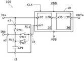
도 1은 반도체 장치의 구성예를 도시한 블록도이다. 반도체 장치(100)는 입력 단자(INa), 입력 단자(INb), 출력 단자(OUTa), 회로(10), 및 회로(RC1)를 포함한다. 단자(INa) 및 단자(INb)는 반도체 장치(100)에 의하여 처리되는 데이터 신호를 입력할 수 있다. 단자(OUTa)는 반도체 장치(100)(회로(10))에 의하여 처리된 데이터 신호를 출력한다.1 is a block diagram showing a configuration example of a semiconductor device. The
<회로(10)><
회로(10)는 회로(20) 및 회로(30)를 포함한다. 회로(10)는 논리 회로로서 기능할 수 있는 반도체 장치이다. 클럭 신호(CLK) 등의 제어 신호, 고전원 전위(VDD), 및 저전원 전위(VSS)는 회로(10)에 입력된다. 회로(10)는 클럭 게이팅 및 파워 게이팅을 사용할 수 있는 회로 블록이다. 클럭 신호(CLK)의 공급은 반도체 장치(100)가 포함되는 반도체 장치의 클럭 게이팅 회로에 의하여 제어되고, 전원 전위(VDD)의 공급은 반도체 장치의 파워 게이팅 회로에 의하여 제어된다.
회로(20)는 선택 회로로서 기능할 수 있고, 입력 단자(a20)로부터의 입력 신호 및 입력 단자(a21)로부터의 입력 신호 중 한쪽을 선택하고 출력 단자(b20)로부터 출력하는 기능을 갖는다. 단자(a20)는 단자(INa)에 전기적으로 접속되고, 단자(a21)는 회로(RC1)의 출력 단자(b1)에 전기적으로 접속되고, 단자(b20)는 회로(30)의 입력 단자(a30)에 전기적으로 접속된다. 회로(30)의 출력 단자(b30)는 단자(OUTa)에 전기적으로 접속된다.The
회로(30)는 데이터(상태)를 유지할 수 있는 회로가 될 수 있다. 회로(30)의 대표적인 예는 순서 회로이다. 이 경우, 단자(b30)로부터 출력된 데이터 신호의 논리 레벨은 단자(a30)에 입력된 데이터 신호에 의하여 결정되거나, 또는 그 데이터 신호 및 회로(30)에 유지된 데이터(상태)에 의하여 결정된다. 회로(30)는 예를 들어 래치 회로, 플립플롭 회로, 시프트 레지스터, 카운터 회로, 또는 분할 회로 등의 순서 회로일 수 있다.The
<회로(RC1)><Circuit (RC1)>
회로(RC1)는 데이터(상태)를 유지할 수 있는 유지 회로로서 기능한다. 회로(RC1)는 노드(FN1), 입력 단자(a1), 입력 단자(a2), 입력 단자(c1), 출력 단자(b1), 스위치(SW1), 스위치(SW2), 스위치(SW3), 및 커패시터(CP1)를 포함한다.The circuit RC1 functions as a holding circuit capable of holding data (state). The circuit RC1 includes a node FN1, an input terminal a1, an input terminal a2, an input terminal c1, an output terminal b1, a switch SW1, a switch SW2, a switch SW3, and A capacitor CP1 is included.
노드(FN1)는 전기적으로 플로팅 상태가 될 수 있도록 제공되고, 회로(RC1)의 데이터(상태) 유지부로서 기능하는 노드이다. 단자(a1)는 단자(INa)에 전기적으로 접속되고, 단자(a2)는 단자(INb)에 전기적으로 접속된다.The node FN1 is provided to be electrically floating state and functions as a data (state) holding unit of the circuit RC1. The terminal a1 is electrically connected to the terminal INa, and the terminal a2 is electrically connected to the terminal INb.
스위치(SW1)는 노드(FN1)와 단자(a1) 사이의 도통을 제어할 수 있다. 스위치(SW2)는 노드(FN1)와 단자(b1) 사이의 도통을 제어할 수 있다. 스위치(SW3)는 단자(a2)와 단자(b1) 사이의 도통을 제어할 수 있다. 커패시터(CP1)의 제 1 단자와 제 2 단자는 각각 노드(FN1) 및 단자(c1)에 전기적으로 접속된다. 노드(FN1) 및 단자(c1)는 커패시터(CP1)에 의하여 용량 결합된다. 따라서, 노드(FN1)의 전위는 단자(c1)의 전위에 의하여 제어될 수 있다. 노드(FN1)가 전기적으로 플로팅인 경우, 예를 들어 단자(c1)의 전위의 증가는 노드(FN1)의 전위를 승압시킬 수 있다.The switch SW1 may control conduction between the node FN1 and the terminal a1 . The switch SW2 may control conduction between the node FN1 and the terminal b1 . The switch SW3 may control conduction between the terminal a2 and the terminal b1 . The first terminal and the second terminal of the capacitor CP1 are electrically connected to the node FN1 and the terminal c1, respectively. The node FN1 and the terminal c1 are capacitively coupled by a capacitor CP1. Accordingly, the potential of the node FN1 can be controlled by the potential of the terminal c1. When the node FN1 is electrically floating, for example, an increase in the potential of the terminal c1 may boost the potential of the node FN1 .
회로(RC1)는 단자(a1)로부터 입력된 데이터 및 단자(a2)로부터 입력된 데이터 중 하나를 선택하고 선택된 데이터를 노드(FN1)에서 유지하는 기능을 갖고, 노드(FN1)에서 유지된 데이터를 단자(b1)로부터 출력하는 기능을 갖는다. 단자(a1)로부터 입력된 데이터를 기록할 때에는, 스위치(SW1)는 온되고 스위치(SW2) 및 스위치(SW3)는 오프된다. 단자(a2)로부터 입력된 데이터를 기록할 때, 스위치(SW2) 및 스위치(SW3)는 온되고 스위치(SW1)는 오프된다. 데이터 판독 시에는, 스위치(SW2)는 온되고 스위치(SW1) 및 스위치(SW3)는 오프된다. 데이터 유지 시에는, 스위치(SW1) 및 스위치(SW2)는 오프되고 노드(FN1)는 전기적으로 플로팅이 된다.The circuit RC1 has a function of selecting one of the data inputted from the terminal a1 and the data inputted from the terminal a2 and holding the selected data at the node FN1, and the data held at the node FN1. It has a function of outputting from the terminal b1. When writing data input from the terminal a1, the switch SW1 is turned on and the switch SW2 and the switch SW3 are turned off. When writing data input from the terminal a2, the switch SW2 and the switch SW3 are turned on and the switch SW1 is turned off. When reading data, the switch SW2 is turned on and the switch SW1 and the switch SW3 are turned off. During data retention, the switch SW1 and the switch SW2 are turned off and the node FN1 is electrically floating.
커패시터(CP1)의 정전기 용량은 RC1에 유지된 데이터가 기록되는 노드(도 1의 경우의 단자(a30)에 상당하는 노드)의 부하를 고려하여 설정된다.The electrostatic capacity of the capacitor CP1 is set in consideration of the load of the node (the node corresponding to the terminal a30 in the case of Fig. 1) in which the data held in RC1 is written.
회로(RC1)는 회로(10)에 유지된 데이터를 위한 백업 기억 회로로서 기능할 수 있다. 이 이유로, 회로(RC1)는, 전원이 차단되는 동안, 저장된 데이터가 유지될 수 있는 유지 특성을 갖는다. 장기간 동안 RC1에 데이터를 유지하기 위하여, 전기적 플로팅의 노드(FN1)의 전위 변화(특히 전위 강하)는 가능한 한 저감되는 것이 바람직하다. 이것을 달성하는 수단은 각 스위치(SW1) 및 스위치(SW2)로서, 오프 상태의 드레인 전류(오프 상태 전류)가 극히 낮은 트랜지스터를 사용하는 것이다.The circuit RC1 may function as a backup storage circuit for the data held in the
트랜지스터의 오프 상태 전류를 저감하기 위하여, 반도체 영역은 예를 들어 넓은 에너지 갭을 갖는 반도체를 포함한다. 이 경우, 반도체의 에너지 갭은 2.5eV 이상, 2.7eV 이상, 또는 3eV 이상인 것이 바람직하다. 이런 반도체의 예는 산화물 반도체이다. 스위치(SW1) 및 스위치(SW2)는 각각 예를 들어 반도체 영역이 산화물 반도체층으로 형성되는 트랜지스터(OS 트랜지스터)이다. 채널 폭으로 정규화된 OS 트랜지스터의 누설 전류는 예를 들어, 실온(약 25℃)에서 10V의 소스-드레인 전압으로 10×10-21A/μm(10zA/μm) 이하가 될 수 있다. 각 스위치(SW1) 및 스위치(SW2)로서 사용된 OS 트랜지스터의 누설 전류는 실온(약 25℃)에서 1×10-18A 이하, 1×10-21A 이하, 또는 1×10-24A 이하가 되는 것이 바람직하다. 또는, 누설 전류는 85℃에서 1×10-15A 이하, 1×10-18A 이하, 또는 1×10-21A 이하가 되는 것이 바람직하다.In order to reduce the off-state current of the transistor, the semiconductor region includes, for example, a semiconductor with a wide energy gap. In this case, the energy gap of the semiconductor is preferably 2.5 eV or more, 2.7 eV or more, or 3 eV or more. An example of such a semiconductor is an oxide semiconductor. Each of the switch SW1 and SW2 is a transistor (OS transistor) in which, for example, a semiconductor region is formed of an oxide semiconductor layer. The leakage current of the OS transistor normalized to the channel width can be, for example,less than or equal to 10×10 -21 A/μm (10zA/μm) with a source-drain voltage of 10V at room temperature (about 25°C). The leakage current of each switch SW1 and the OS transistor used as the switch SW2 is 1×10-18 A or less, 1×10-21 A or less, or 1×10-24 A or less at room temperature (about 25° C.) It is preferable to be Alternatively, the leakage current is preferably 1×10-15 A or less, 1×10-18 A or less, or 1×10-21 A or less at 85°C.
산화물 반도체가 넓은 에너지 갭을 갖고 전자가 여기되기 어려우며 정공의 유효 질량은 크기 때문에, OS 트랜지스터에서는 실리콘 등을 포함하는 일반적인 트랜지스터보다 애벌란시 항복(Avalanche breakdown)이 일어나기 어렵다. 애벌란시 항복으로 인한 핫 캐리어 열화 등이 억제되므로, OS 트랜지스터는 높은 드레인 내전압을 갖고 높은 드레인 전압으로 구동될 수 있다. 따라서, 회로(RC1)에 OS 트랜지스터를 사용함으로써, 신호의 전위 레벨 및 입력 타이밍 등의 구동 조건의 여유도(margin)를 넓게 할 수 있다. 회로(RC1)는, 예를 들어, 데이터가 유지될 때 노드(FN1)의 전위가 높게 되도록 구동될 수 있다.Since the oxide semiconductor has a wide energy gap, electrons are difficult to be excited, and the effective mass of holes is large, avalanche breakdown is less likely to occur in the OS transistor than in a general transistor including silicon or the like. Since degradation of hot carriers due to avalanche breakdown is suppressed, the OS transistor has a high drain withstand voltage and can be driven with a high drain voltage. Therefore, by using the OS transistor for the circuit RC1, the margin of driving conditions such as the signal potential level and input timing can be widened. The circuit RC1 may be driven such that the potential of the node FN1 becomes high when data is held, for example.
또한, OS 트랜지스터는 게이트 절연층이 약 11nm의 등가 산화물 두께를 갖고 채널 길이가 50nm로 짧더라도 우수한 오프 상태 전류 특성 및 서브스레숄드(subthreshold) 특성을 가질 수 있다. OS 트랜지스터의 게이트 절연층은 논리 회로에 일반적으로 사용된 Si 트랜지스터보다 두꺼울 수 있으므로, 게이트 절연층을 통한 누설 전류를 저감할 수 있고 게이트 절연층의 두께의 차이로 인한 전기 특성의 변화를 억제할 수 있다. OS 트랜지스터의 자세한 사항은 실시형태 2에서 설명할 것이다.In addition, the OS transistor may have excellent off-state current characteristics and subthreshold characteristics even if the gate insulating layer has an equivalent oxide thickness of about 11 nm and the channel length is as short as 50 nm. Since the gate insulating layer of the OS transistor can be thicker than the Si transistor generally used in logic circuits, the leakage current through the gate insulating layer can be reduced and changes in electrical characteristics caused by the difference in the thickness of the gate insulating layer can be suppressed. there is. The details of the OS transistor will be described in Embodiment 2.
스위치(SW3), 및 회로(10)에 포함되는 트랜지스터에 특별히 한정은 없고, 논리 회로에 포함되는 일반적인 트랜지스터가 사용될 수 있고; 예를 들어, 반도체 영역이 제 4 족 원소(Si, Ge, 또는 C)를 함유하는 트랜지스터를 사용할 수 있다. 회로(10)의 트랜지스터의 대표적인 예는 반도체 영역이 실리콘을 함유한 트랜지스터(Si 트랜지스터)이다. Si 트랜지스터의 이동도를 향상시키는 목적 또는 다른 목적을 위하여, Si 트랜지스터의 반도체 영역에 Ge를 첨가하여 얻어진 왜곡 트랜지스터(distortion transistor)를 사용하여도 좋다.There is no particular limitation on the transistors included in the switch SW3 and the
스위치(SW3)는 스위치(SW1) 및 스위치(SW2)와 같은 OS 트랜지스터가 되어도 좋고, 또는 아날로그 스위치 등 스위치 회로가 되어도 좋다. OS 트랜지스터가 스위치(SW3)로서 사용되는 경우, 회로(RC1)의 추가로 인한 반도체 장치(100)의 면적 오버헤드는 이하에서 설명한 바와 같이 제로가 될 수 있다. 한편, 아날로그 스위치가 스위치(SW3)로서 사용되는 경우, Si 트랜지스터는 p채널 트랜지스터에 사용되고, OS 트랜지스터는 n채널 트랜지스터에 사용되고, n채널 트랜지스터는 p채널 트랜지스터 위에 적층되고, 이 경우, 반도체 장치(100)의 면적은 스위치(SW3)가 Si 트랜지스터만으로 형성되는 경우에 비하여 축소될 수 있다.The switch SW3 may be an OS transistor like the switches SW1 and SW2, or may be a switch circuit such as an analog switch. When the OS transistor is used as the switch SW3 , the area overhead of the
반도체 장치(100)에서, 회로(RC1)의 제공에 의한 회로(20) 및 회로(30)의 회로 구성의 변경은 불필요하다. 또한 셀렉터 또는 멀티플렉서 등 일반적인 선택 회로는 회로(20)로서 사용될 수 있다. 또한, 래치 회로 또는 플립플롭 회로 등 일반적인 순서 회로는 회로(30)로서 사용될 수 있다. 회로(RC1)는 회로(20) 및 회로(30) 위에 적층될 수 있기 때문에, 회로(20) 및 회로(30)의 레이아웃의 변경이 거의 없이 회로(RC1)가 제공될 수 있다. 본 실시형태에서, OS 트랜지스터를 포함하는 회로 블록이 선택 회로 및 순서 회로를 포함하는 회로 블록 위에 적층됨으로써, OS 트랜지스터를 포함하는 회로 블록의 추가로 인한 면적 오버헤드 및 선택 회로와 순서 회로의 통상 동작 중의 성능 페널티는 제로가 될 수 있다.In the
반도체 장치(100)의 구체적인 회로 구성 및 구동 방법의 예에 대하여 아래에서 설명할 것이다.An example of a specific circuit configuration and driving method of the
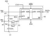
≪반도체 장치의 구성예 2≫«Semiconductor device configuration example 2»
도 2는 반도체 장치의 구성예를 도시한 회로도이다. 도 3 및 도 4는 각각 도 2에 도시된 반도체 장치의 구동 방법의 예를 나타낸 타이밍 차트이다. 도 2의 회로도는 도 1에 도시된 반도체 장치(100)의 구체적인 예이다. 도 2에 도시된 반도체 장치(101)는 회로(11) 및 회로(RC2)를 포함한다.2 is a circuit diagram showing a configuration example of a semiconductor device. 3 and 4 are timing charts each showing an example of a method of driving the semiconductor device shown in FIG. 2 . The circuit diagram of FIG. 2 is a specific example of the
회로(11)는 도 1의 회로(10)에 상당하는 회로 블록이다. 회로(11)는 회로(SELC1) 및 플립플롭 회로(FF)(31)를 포함한다.The
SELC1은 하나의 인버터(NOT 게이트) 회로 및 두 개의 아날로그 스위치 회로를 포함하고 선택 회로로서 기능할 수 있다. SELC1에는, 제어 신호로서의 신호(SEL) 및 전원 전위(VDD 및 VSS)가 입력된다.SELC1 includes one inverter (NOT gate) circuit and two analog switch circuits and can function as a selection circuit. A signal SEL as a control signal and power source potentials VDD and VSS are input to SELC1.
FF(31)에, 클럭 신호(CLK) 및 리셋 신호(RESET)는 제어 신호로서 입력되고 VDD 및 VSS는 전원 전위로서 입력된다. 신호(CLKB)는 CLK의 반전 신호이고 회로(11)에 제공된 인버터 회로 등에 의하여 CLK로부터 생성된다. 도 2에서, FF(31)는 마스터 슬레이브 FF이고 두 개의 래치 회로를 포함한다(LATa 및 LATb). LATa는 하나의 아날로그 스위치, 하나의 NAND 게이트 회로, 및 하나의 클럭드 인버터 회로를 포함한다. LATb는 하나의 아날로그 스위치, 하나의 인버터 회로, 및 하나의 클럭드 NAND 게이트 회로를 포함한다. FF(31)에서, 하나의 아날로그 스위치 및 하나의 인버터 회로는 클럭드 인버터 회로 대신에 제공될 수 있고, 하나의 아날로그 스위치 및 NAND 게이트 회로는 클럭드 NAND 게이트 회로 대신 제공될 수 있다.To the FF 31, a clock signal CLK and a reset signal RESET are input as control signals, and VDD and VSS are input as a power supply potential. The signal CLKB is an inverted signal of CLK and is generated from CLK by an inverter circuit provided in the
회로(RC2)는 도 1의 회로(RC1)에 상당한다. 트랜지스터(Mos1), 트랜지스터(Mos2), 및 트랜지스터(Mos3)는 각각 SW1, SW2, 및 SW3으로서 기능하고, n채널 트랜지스터 및 OS 트랜지스터이다. 신호(OG1)~(OG3)는 트랜지스터(Mos1)~(Mos3)의 온/오프를 제어하기 위한 제어 신호이다. 신호(CSB)는 커패시터(CP1)의 제 2 단자에 입력된다.Circuit RC2 corresponds to circuit RC1 in FIG. 1 . The transistor Mos1, the transistor Mos2, and the transistor Mos3 function as SW1, SW2, and SW3, respectively, and are an n-channel transistor and an OS transistor. Signals OG1 to OG3 are control signals for controlling on/off of transistors Mos1 to Mos3. The signal CSB is input to the second terminal of the capacitor CP1.
도 2에 도시된 반도체 장치(101)는 스캔 플립플롭 회로로서 기능할 수 있고, 예를 들어 복수의 반도체 장치(101)는 스캔 체인을 형성할 수 있다. 이 경우, 단자(INa)는 통상 동작을 위한 데이터 입력 단자로서 사용되고, 단자(INb)는 스캔 체인의 입력부로서 사용된다. 스캔 체인을 형성하기 위하여, 두 개의 인접된 반도체 장치(101) 중 한쪽의 입력 단자(INb)가 다른 쪽의 반도체 장치(101)의 출력 단자(OUTa)와 전기적으로 접속된다. 복수의 반도체 장치(101) 각각의 입력 단자(INa)는 조합 회로의 출력 단자와 접속된다.The
반도체 장치(101)는 예를 들어 FPGA 등의 PLD(programmable logic device)의 논리 소자로서 사용될 수 있다. 논리 소자에 포함된 레지스터 및 레지스터의 입력 신호를 선택하기 위한 선택 회로를 갖는 회로 블록은 회로(11)를 사용하여 형성되어도 좋다. 이 경우, 복수의 반도체 장치(101)는 백업 기능을 갖는 레지스터 체인을 형성할 수 있다.The
반도체 장치(101)는 클럭 게이팅 및 파워 게이팅을 사용할 수 있으므로, 회로(11)가 포함되는 반도체 장치에서 회로(11)의 동작이 불필요한 기간에 회로(11)에 대한 CLK 및 VDD의 공급이 정지될 수 있다. 결과로서, 반도체 장치(101)의 동적 소비 전력을 저감시킬 수 있다. 이하에서, 반도체 장치(101)의 구동 방법의 예에 대하여 도 3 및 도 4를 참조하여 설명한다.Since the
도 3 및 도 4는 제어 신호(OG1)~(OG3), (CSB), (CLK), (RESET), 및 (SEL), 입력 신호(D0) 및 (SC), 및 출력 신호(Q0)의 파형; 노드(FN1)의 전위 변화; 및 회로(11)의 전원 전위(VDD)를 위한 입력 단자의 전위 변화를 나타낸 것이다. 반도체 장치(101)에 입력된 신호(OG1)~(OG3), (CSB), (CLK), (RESET), (SEL), (D0), 및 (SC)는, 도 3 및 도 4의 예에서, 하이(H) 레벨 전위가 VDD, 로(L) 레벨 전위가 VSS이다.3 and 4 show control signals OG1 to (OG3), (CSB), (CLK), (RESET), and (SEL), input signals D0 and (SC), and output signals Q0. waveform; potential change of node FN1; and the potential change of the input terminal for the power supply potential VDD of the
≪반도체 장치의 구동 방법의 예 1≫«Example 1 of a method for driving a semiconductor device»
도 3은 클럭 게이팅 및 파워 게이팅을 제어하기 위한 방법의 예를 나타낸 것이다.3 shows an example of a method for controlling clock gating and power gating.
<기간(T1)><Period (T1)>
기간(T1)에, 반도체 장치(101)는 통상 동작 모드에서 동작한다. 통상 동작에서, 반도체 장치(101)(회로(11))는 플립플롭 회로로서 동작한다. 도 3에 나타낸 예에서, 통상 동작의 반도체 장치(101)는, 신호(D0)의 상태가 FF(31)에 유지되도록 동작한다.In the period T1, the
또한, VDD 및 CLK는 회로(11)에 공급된다. 신호(SEL)의 전위가 L 레벨이기 때문에, FF(31)의 입력 단자(a30)와 단자(INa)의 도통은 SELC1을 통하여 확립된다. FF(31)의 상태(출력 신호(Q0))는 신호(CLK) 및 단자(a30)로부터 입력되는 신호(D0)에 따라 변화된다.Further, VDD and CLK are supplied to the
통상 동작에서, 노드(FN1)의 전위는 논리 레벨이 "L"이 되는 전위로 유지된다. 여기서 노드(FN1)의 논리 레벨은 단자(INb)로부터 입력된 신호(SC)를 이용하여 "L"로 유지된다. 구체적으로, SC의 전위는 L 레벨(VSS)로 설정되고 트랜지스터(Mos2) 및 (Mos3)는 온된다. 따라서, 노드(FN1)의 전위는 VSS가 된다. 즉, 통상 동작에서, 노드(FN1)는 신호(SC)를 사용하여 프리차지된다. 또한, SC의 L레벨 전위는 VSS에 한정되지 않지만, SC의 L 레벨 전위가 VSS일 때, 신호(SC)는 사용되는 전원 전위 수를 증가시키지 않고 발생될 수 있다.In normal operation, the potential of the node FN1 is maintained at a potential at which the logic level becomes "L". Here, the logic level of the node FN1 is maintained at "L" using the signal SC input from the terminal INb. Specifically, the potential of SC is set to the L level (VSS) and the transistors Mos2 and Mos3 are turned on. Accordingly, the potential of the node FN1 becomes VSS. That is, in normal operation, the node FN1 is precharged using the signal SC. Further, the L-level potential of SC is not limited to VSS, but when the L-level potential of SC is VSS, the signal SC can be generated without increasing the number of power supply potentials used.
<기간(T2)><Period (T2)>
기간 T2에, VDD는 공급되고 CLK는 공급되지 않으므로, 반도체 장치(101)는 대기 상태에 있다. RC2는 FF(31)의 상태를 백업한다. 구체적으로는, FF(31)에 입력된 데이터 신호(D0)의 논리 레벨이 RC2에 기록된다.In the period T2, since VDD is supplied and CLK is not supplied, the
먼저, 트랜지스터(Mos2) 및 트랜지스터(Mos3)가 오프되어 노드(FN1)를 전기적으로 플로팅으로 하고 신호(CSB)가 H 레벨로 설정됨으로써, 노드(FN1)의 전위는 논리 레벨이 "H"가 되는 전위로 승압된다. 그리고, 트랜지스터(Mos1)는 온되어 신호(D0)는 노드(FN1)에 입력된다. 신호(D0)의 논리 레벨이 "L"이 될 때, 노드(FN1)의 전하가 단자(INa)에 추출된다. 따라서, 노드(FN1)의 전위는 하강되고 노드(FN1)의 논리 레벨은 "L"이 된다. 신호(D0)의 논리 레벨이 "H"가 될 때, 노드(FN1)의 전하는 저장되고 노드(FN1)의 논리 레벨은 "H"가 유지된다.First, the transistor Mos2 and the transistor Mos3 are turned off to make the node FN1 electrically floating and the signal CSB is set to the H level, so that the potential of the node FN1 becomes "H" at the logic level. is boosted to potential. Then, the transistor Mos1 is turned on and the signal D0 is input to the node FN1. When the logic level of the signal D0 becomes "L", the charge of the node FN1 is extracted to the terminal INa. Accordingly, the potential of the node FN1 falls and the logic level of the node FN1 becomes "L". When the logic level of the signal D0 becomes "H", the charge of the node FN1 is stored and the logic level of the node FN1 is maintained at "H".
상술한 바와 같이, 노드(FN1)의 전하는, 데이터 L이 기록될 때에만, 노드(FN1)의 논리 레벨을 "L"로 하기 위한 프리차지 동작 및 용량 결합에 의한 노드(FN1)의 승압 동작 때문에 RC2의 백업 동작 중에 이동한다. 따라서, 백업 동작을 고속으로 실행할 수 있어, CLK의 공급 정지 후에 단기간 안에 VDD의 공급을 정지하는 것을 가능하게 한다. 게다가, 데이터 H가 기록되는 경우, 트랜지스터(Mos1)의 문턱 전압에 의한 노드(FN1)의 전압 강하는 일어나지 않는다. 결과적으로, 트랜지스터(Mos1)의 제어 신호(OG1)의 H 레벨 전위는 VDD보다 높게 설정될 필요는 없다.As described above, the charge of the node FN1 is due to the precharge operation for setting the logic level of the node FN1 to "L" only when the data L is written, and the step-up operation of the node FN1 by capacitive coupling. Moves during backup operation of RC2. Therefore, the backup operation can be executed at high speed, making it possible to stop the supply of VDD within a short period of time after the supply of CLK is stopped. In addition, when the data H is written, the voltage drop of the node FN1 by the threshold voltage of the transistor Mos1 does not occur. Consequently, the H level potential of the control signal OG1 of the transistor Mos1 need not be set higher than VDD.
트랜지스터(Mos1)가 일정 기간 온된 후, 트랜지스터(Mos1)는 오프되어 노드(FN1)를 전기적으로 플로팅으로 한다. 이런 식으로, FF(31)의 백업은 완료된다.After the transistor Mos1 is turned on for a predetermined period, the transistor Mos1 is turned off to make the node FN1 electrically floating. In this way, the backup of the FF 31 is completed.
도 3에 나타낸 예에서, OG1은 CSB 후에 H 레벨로 설정된다. 그러나, CSB 및 OG1은 동시에 H 레벨로 변화되어도 좋고, 예를 들어 이 경우 백업 동작에 필요한 시간을 저감시킬 수 있다.In the example shown in Fig. 3, OG1 is set to H level after CSB. However, CSB and OG1 may be simultaneously changed to H level, for example, in this case, the time required for the backup operation can be reduced.
<기간(T3)><Period (T3)>
기간(T3)에 VDD의 공급이 정지되고 반도체 장치(101)가 정지된다. OG1 및 RESET가 L 레벨로 설정된 후, VDD의 공급이 정지된다.In the period T3, the supply of VDD is stopped and the
<기간(T4)><Period (T4)>
반도체 장치(101)를 다시 통상 동작으로 하기 위하여, 먼저, VDD의 공급이 재개된다. VDD의 공급이 재개될 때, 단자(a20)와 단자(a30) 사이의 도통이 SELC1을 통하여 확립된다.In order to put the
<기간(T5)><Period (T5)>
FF(31)는 CLK의 공급이 정지되기 전의 상태로 복귀된다. 구체적으로, RC2에 유지된 데이터는 FF(31)에 기록된다. 먼저, SEL 및 OG3은 H 레벨로 설정되어, 단자(INb)와 FF(31)의 입력 단자(a30) 사이의 도통이 확립되고, 신호(SC)는 H 레벨로 설정된다. 따라서, 단자(a30)의 논리 레벨은 "H"가 된다. 다음에, 트랜지스터(Mos2)는 온되어 노드(FN1)와 단자(a30) 사이의 도통이 확립된다. 노드(FN1)의 논리 레벨이 "L"이 될 때, 단자(a30)의 전위는 L 레벨이 된다. 따라서, 단자(a30)의 논리 레벨은 "L"이 된다. 노드(FN1)의 논리 레벨이 "H"가 되면, 단자(a30)의 전위는 거의 변화되지 않으므로, 단자(a30)의 논리 레벨은 "H"가 유지된다. 상술한 식으로, FF(31)의 상태는 노드(FN1)에서 유지된 상태로 설정될 수 있다. 이것은, FF(31)는 CLK의 공급 정지 직전의 상태로 복귀될 수 있다.The FF 31 is returned to the state before the supply of CLK was stopped. Specifically, data held in RC2 is written to FF 31 . First, SEL and OG3 are set to the H level, conduction between the terminal INb and the input terminal a30 of the FF 31 is established, and the signal SC is set to the H level. Accordingly, the logic level of the terminal a30 becomes "H". Next, the transistor Mos2 is turned on to establish conduction between the node FN1 and the terminal a30. When the logic level of the node FN1 becomes "L", the potential of the terminal a30 becomes the L level. Accordingly, the logic level of the terminal a30 becomes "L". When the logic level of the node FN1 becomes "H", the potential of the terminal a30 hardly changes, so that the logic level of the terminal a30 is maintained at "H". In the manner described above, the state of the FF 31 can be set to the state maintained in the node FN1. This allows the FF 31 to return to the state immediately before the stop of supply of CLK.
상술한 바와 같이, 단자(a30)의 논리 레벨이 RC2의 복귀 동작 중에 "H"로 설정된 후, RC2에 유지된 데이터가 FF(31)에 기록되므로, 노드(FN1)의 전하는 데이터 L이 FF(31)에 기록될 때에만 이동한다. 결과적으로, 복귀 동작이 고속으로 실행될 수 있어, VDD의 공급의 재개 후에 단기간 안에 반도체 장치(101)의 통상 동작을 가능하게 한다. 게다가, 데이터 H가 기록되는 경우, 트랜지스터(Mos2)의 문턱 전압에 의한 단자(a30)의 전압 강하는 일어나지 않는다. 따라서, 트랜지스터(Mos2)의 제어 신호(OG2)의 H 레벨 전위는 VDD보다 높게 설정될 필요는 없다.As described above, after the logic level of the terminal a30 is set to "H" during the recovery operation of RC2, the data held in RC2 is written to the FF31, so that the charge of the node FN1 is transferred from the data L to FF( It moves only when it is recorded in 31). As a result, the recovery operation can be performed at high speed, enabling the normal operation of the
단자(a30)의 논리 레벨을 "H"로 설정하는 동작은 FF(31)의 회로 구성 또는 전원이 정지될 때의 상태의 영향을 받지 않는다. 이것은 다양한 순서 회로 중 어느 것이 회로(11)로서 사용될 수 있는 것을 뜻한다. 상술한 바와 같이, 본 실시형태의 유지 회로는 폭넓게 사용될 수 있으므로, 파워 게이팅을 위한 데이터 유지 기능이 다양한 순서 회로에 추가될 수 있다.The operation of setting the logic level of the terminal a30 to "H" is not affected by the circuit configuration of the FF 31 or the state when the power supply is stopped. This means that any of the various sequence circuits can be used as
<기간(T6)><Period (T6)>
CLK의 공급이 재개되어 반도체 장치(101)는 통상 동작한다. CLK의 공급이 재개되기 전의 기간(T5)에, 신호(RESET)는 H 레벨로 설정된다. 기간(T6)의 반도체 장치(101)의 구동 방법은 기간(T1)과 마찬가지이므로 설명은 생략한다.The supply of CLK is resumed, and the
상술한 바와 같이, 노드(FN1)의 프리차지 동작, RC2의 저장 동작, 및 RC2의 복귀 동작에서, 트랜지스터(Mos1)~(Mos3)의 문턱 전압은 RC2 또는 FF(31)에 기록된 데이터의 논리 레벨에 영향을 미치지 않는다. 따라서, 트랜지스터(Mos1)~(Mos3)가 OS 트랜지스터인 경우에도, 이들 트랜지스터의 제어 신호(OG1)~(OG3)의 H 레벨 전위를 회로(11)의 VDD와 같은 전위로 할 수 있다. 바꿔 말하면, RC2가 반도체 장치(101)에 제공되는 경우에도, 동작에 필요한 전위의 수는 증가되지 않는다.As described above, in the precharge operation of the node FN1 , the storage operation of RC2 , and the return operation of RC2 , the threshold voltages of the transistors Mos1 to Mos3 are the logic of the data written to RC2 or FF31 . Doesn't affect level. Accordingly, even when the transistors Mos1 to Mos3 are OS transistors, the H level potential of the control signals OG1 to OG3 of these transistors can be set to the same potential as VDD of the
≪반도체 장치의 구동 방법의 예 2≫«Example 2 of a method for driving a semiconductor device»
도 3에 나타낸 구동 방법의 예에서, RC2는 단자(INa)에 입력된 데이터 신호(D0)를 백업한다. RC2는 단자(INb)에 입력된 신호(SC)를 백업할 수도 있다. 도 4는 이런 구동 방법의 예를 나타낸 것이다. 도 4의 구동 방법 예에서, 도 3의 구동 방법의 예와 같은 동작의 설명은 생략한다. 따라서, 설명에는, 도 3의 설명을 원용한다.In the example of the driving method shown in Fig. 3, RC2 backs up the data signal D0 input to the terminal INa. RC2 may back up the signal SC input to the terminal INb. 4 shows an example of such a driving method. In the driving method example of FIG. 4 , descriptions of the same operations as in the driving method example of FIG. 3 are omitted. Therefore, the description of FIG. 3 is used for description.
<기간(T11)><Period (T11)>
기간(T11)에, 반도체 장치(101)는 통상 동작 모드이다. 기간(T11)은 신호(D0)의 논리 레벨이 "L"을 유지하는 점에서 도 3의 기간(T1)과 다르다. 물론, 기간(T11)의 신호(D0)는 도 3에 나타낸 바와 같이 논리 레벨이 변화되는 데이터 신호가 될 수 있다.In the period T11, the
<기간(T12)><Period (T12)>
단자(INb)에 입력된 데이터 신호는 백업된다. CLK의 공급이 정지된 후, 먼저, 노드(FN1)의 전위는 승압되어 노드(FN1)의 논리 레벨은 "H"가 된다. 이를 달성하기 위하여, 트랜지스터(Mos1)~(Mos3)는 오프되고 신호(CSB)는 H 레벨로 설정된다. 그리고, 트랜지스터(Mos2) 및 트랜지스터(Mos3)는 온되고 신호(SC)는 노드(FN1)에 기록된다.The data signal input to the terminal INb is backed up. After the supply of CLK is stopped, first, the potential of the node FN1 is boosted so that the logic level of the node FN1 becomes "H". To achieve this, transistors Mos1 to Mos3 are turned off and signal CSB is set to H level. Then, the transistor Mos2 and the transistor Mos3 are turned on and the signal SC is written to the node FN1.
<기간(T13)><Period (T13)>
기간(T13)에, 반도체 장치(101)는 도 3의 기간(T3)과 같은 식으로 동작한다. 트랜지스터(Mos2) 및 트랜지스터(Mos3)는 오프되고 VDD의 공급은 정지된다. RC2는 기간(T12)에서 단자(INb)에 입력된 데이터를 유지한다.In the period T13 , the
<기간(T14), 기간(T15)><Period (T14), Period (T15)>
반도체 장치(101)는 도 3의 기간(T4) 및 기간(T5)과 같은 식으로 동작한다. VDD의 공급이 재개되고, RC2에 유지된 데이터는 FF(31)의 입력 단자(a30)에 기록되고, FF(31)의 상태는 복귀된다. 따라서, CLK의 공급이 재개되어 반도체 장치(101)는 통상 동작한다.The
<기간(T16)><Period (T16)>
기간(T16)에, 반도체 장치(101)는 통상 동작한다. 기간(T16)은, 단자(INb)와 단자(a21) 사이의 도통이 트랜지스터(Mos3)를 통하여 확립되는 점 및 신호(SEL)가 H 레벨로 설정되어 단자(a30)와 단자(a21) 사이의 도통이 SELC1을 통하여 확립되는 점에서 도 3의 기간(T6)과 다르다. 따라서, 단자(INb)에 입력된 데이터 신호(SC)는 FF(31)에 입력된다.In the period T16, the
반도체 장치(101)가 스캔 FF로서 동작하는 경우, 예를 들어, 테스트 데이터는 기간(T12)에 단자(INb)에 입력된다. 예를 들어, 반도체 장치(101)(RC1)에 테스트 패턴을 입력하는 스캔-인(Scan-in) 동작을 기간(T12)에 수행하고, 기간(T16)에 시프트 동작을 수행할 수 있다. 이 경우, 반도체 장치(101)는 도 4에 나타낸 바와 같이 동작하여, RC2에 유지된 데이터가 정상적인지 여부는 회로(11)(스캔 FF)의 출력 신호(Q0)의 논리 값으로부터 판정될 수 있으므로, RC2가 문제를 가질지 여부를 판정할 수 있다.When the
도 2의 회로 구성의 예는 선택 회로 및 플립플롭 회로를 포함하는 일반적인 스캔 플립플롭 회로가 회로(11)로서 사용될 수 있는 것을 나타낸다. 도 3 및 도 4의 구동 방법의 예는, 반도체 장치(101)가 일반적인 스캔 FF와 같이 동작할 수 있는 것을 나타낸다.The example of the circuit configuration in FIG. 2 shows that a general scan flip-flop circuit including a selection circuit and a flip-flop circuit can be used as the
따라서, 본 실시형태의 반도체 장치(101)는 스캔 FF(회로(11)) 및 OS 트랜지스터를 갖는 유지 회로(OS 블록)를 포함하는 반도체 장치가 될 수 있다. 일반적인 회로는 스캔 FF로서 사용될 수 있으므로, OS 블록의 추가에 의한 회로 구성 및 레이아웃의 변화를 방지할 수 있다. OS 블록은 OS 트랜지스터 및 커패시터를 사용하여 형성될 수 있어, 스캔 FF 위에 적층될 수 있다. OS 블록이 스캔 FF 위에 적층되는 3차원 구조를 반도체 장치(101)가 갖는 경우, OS 블록의 추가로 인한 레이아웃 면적의 오버헤드 및 통상 동작 중의 성능 페널티가 제로가 될 수 있다.Accordingly, the
상술한 바와 같이, 본 실시형태의 반도체 장치에 의하여, OS 블록이 추가되는 경우에도 성능 오버헤드 및 면적 오버헤드 거의 없이 파워 게이팅에 의하여 반도체 장치(101)의 동적 소비 전력이 저감될 수 있다.As described above, according to the semiconductor device of the present embodiment, even when an OS block is added, the dynamic power consumption of the
≪반도체 장치의 변형예≫«Modified example of semiconductor device»
반도체 장치(100)(도 1)의 일부의 변형예에 대하여 아래에서 설명한다.Modifications of a part of the semiconductor device 100 ( FIG. 1 ) will be described below.
<구성예 3><Configuration Example 3>
도 1에서는, RC1의 입력 단자(a1)는 회로(10)의 입력 단자(a20)(입력 단자(INa))에 전기적으로 접속된다. 단자(a1)가 회로(10)에 접속되는 접속 노드는 단자(a20)에 한정되지 않고, 예를 들어 회로(20)의 출력 단자(b20), 회로(30)의 입력 단자(a30), 회로(30)의 출력 단자(b30), 또는 회로(30)의 내부 노드일 수 있다. 이 경우, 회로(30)의 내부 노드는 단자(a30)와 단자(b30) 사이의 데이터 신호의 전송 경로에서의 노드이다. 도 2에 도시된 FF(31)가 회로(30)로서 사용되는 경우, 예를 들어, 내부 노드는 LATa의 클럭드 인버터 회로의 출력 단자, LATa의 NAND 게이트 회로의 출력 단자, 또는 LATb의 인버터 회로의 출력 단자이다.In FIG. 1 , the input terminal a1 of RC1 is electrically connected to the input terminal a20 (input terminal INa) of the
도 5에 도시된 반도체 장치(111)는 단자(a1)가 단자(b30)에 전기적으로 접속되는 예이다. 이 구성예에서도, 회로(10)의 구성 및 레이아웃의 변경은 도 5에 도시된 바와 같이 불필요하다.The
<구성예 4><Configuration Example 4>
단자(a1)는, RC1의 단자(a1)에 입력된 신호의 논리 레벨을 보상하기 위하여 버퍼부에 전기적으로 접속되어도 좋다. 버퍼부는 하나의 버퍼 회로, 캐스케이드의 버퍼 회로들, 하나의 인버터 회로, 캐스케이드의 인버터 회로들 등이 될 수 있다. 신호(D0)의 논리를 반전하여 얻어지는 데이터가 회로(10)의 구성 등의 제한하에서 도 1의 RC1에 유지될 필요가 있는 경우, 짝수의 인버터 회로가 버퍼부로서 사용된다.The terminal a1 may be electrically connected to the buffer portion in order to compensate the logic level of the signal input to the terminal a1 of the RC1. The buffer unit may be one buffer circuit, cascade buffer circuits, one inverter circuit, cascade inverter circuits, and the like. When data obtained by inverting the logic of the signal D0 needs to be held in RC1 in Fig. 1 under restrictions such as the configuration of the
단자(b1)는, RC1의 단자(b1)로부터의 출력 신호의 논리 레벨을 보상하기 위하여 또는 그 출력 신호의 논리를 반전하기 위하여 버퍼부에 전기적으로 접속될 수도 있다.The terminal b1 may be electrically connected to the buffer portion to compensate the logic level of the output signal from the terminal b1 of RC1 or to invert the logic of the output signal.
도 6의 (A)에 도시된 반도체 장치(112)는 단자(a1)가 하나의 버퍼 회로(52)에 전기적으로 접속되는 예이다. 도 6의 (B)에 도시된 반도체 장치(113)는 단자(b1)가 하나의 인버터 회로(53)에 전기적으로 접속되는 예이다.The
<구성예 5><Configuration Example 5>
도 1에 도시된 회로(RC1)는 하나의 상태를 유지할 수 있지만, 복수의 상태를 유지할 수 있는 유지 회로가 반도체 장치에 제공될 수 있다. 도 7은 이런 구성예를 도시한 것이다. 도 7에 도시된 반도체 장치(114)는 상태의 백업 기억 회로로서, 회로(RC1) 대신 회로(RC14)를 포함한다.Although the circuit RC1 illustrated in FIG. 1 may maintain one state, a holding circuit capable of maintaining a plurality of states may be provided in the semiconductor device. Fig. 7 shows an example of such a configuration. The
RC14는 두 개의 회로(RC1c 및 RC1d)를 추가로 포함하는 RC1에 상당한다. 따라서, RC14는 세 개의 상태를 유지할 수 있다. RC1c 및 RC1d는 RC1과 같은 구성을 갖고, RC1과 같은 식으로 구동될 수 있다. RC1c 및 RC1d는 단자(INa) 및 단자(INb)로부터 입력된 데이터 신호를 유지할 수도 있고 회로(10)에 이들의 유지 상태를 기록할 수 있다. 노드(FN1c) 및 노드(FN1d)는 각각 RC1c 및 RC1d의 데이터 유지 노드이다.RC14 corresponds to RC1 which further includes two circuits RC1c and RC1d. Thus, RC14 can maintain three states. RC1c and RC1d have the same configuration as RC1 and can be driven in the same way as RC1. RC1c and RC1d may hold data signals input from terminals INa and INb and write their holding states to the
RC14에서의 스위치(SW1), (SW1c), (SW1d), (SW2), (SW2c), (SW2d), (SW3), (SW3c), 및 (SW3d)는 독립적으로 온/오프된다. 스위치(SW1), (SW1c), (SW1d), (SW2), (SW2c), 및 (SW2d)는 OS 트랜지스터이다. 스위치(SW3c) 및 (SW3d)는 각각 SW3과 같이 OS 트랜지스터 또는 아날로그 스위치 등의 스위치 회로가 될 수 있다.Switches (SW1), (SW1c), (SW1d), (SW2), (SW2c), (SW2d), (SW3), (SW3c), and (SW3d) in RC14 are independently turned on/off. The switches SW1, SW1c, SW1d, SW2, SW2c, and SW2d are OS transistors. The switches SW3c and SW3d may each be a switch circuit such as an OS transistor or an analog switch, like SW3.
신호(CSB)는 커패시터(CP1), (CP1c), 및 (CP1d)의 제 2 단자에 입력된다. 또는, 노드(FN1), (FN1c), 및 (FN1d)의 전위가 독립적으로 승압될 수 있도록, 커패시터(CP1), (CP1c), 및 (CP1d)의 제 2 단자에 다른 신호가 입력되어도 좋다.The signal CSB is input to the second terminals of the capacitors CP1, CP1c, and CP1d. Alternatively, other signals may be input to the second terminals of the capacitors CP1, CP1c, and CP1d so that the potentials of the nodes FN1, FN1c, and FN1d can be boosted independently.
반도체 장치(114)의 통상 동작에서, 회로(30)의 상태는 RC14에서의 유지 회로(RC1), (RC1c), 및 (RC1d) 중 하나에 기록될 수 있다. 바꿔 말하면, RC14는 통상 동작의 일정 기간에 반도체 장치(114)(회로(30))의 세 개의 상태를 유지할 수 있다.In the normal operation of the
(실시형태 2)(Embodiment 2)
본 실시형태에서, 반도체 장치의 예로서 OS 트랜지스터에 대하여 설명하기로 한다.In this embodiment, an OS transistor will be described as an example of a semiconductor device.
≪OS 트랜지스터의 구조예 1≫«Structure Example 1 of OS Transistor»
도 8의 (A)~(D)는 OS 트랜지스터의 구조예를 도시한 것이다. 도 8의 (A)는 OS 트랜지스터의 구조예를 도시한 상면도이다. 도 8의 (B)는 선 y1-y2를 따르는 단면도이고, 도 8의 (C)는 선 x1-x2를 따르는 단면도이고, 도 8의 (D)는 선 x3-x4를 따르는 단면도이다. 디바이스의 구조를 명확화하기 위하여, 도 8의 (A)는 일부 구성 요소를 도시하지 않았다. 여기서, 선 y1-y2의 방향은 채널 길이 방향이라고 하고, 선 x1-x2의 방향은 채널 폭 방향이라고 하는 경우가 있다. 따라서, 도 8의 (B)는 채널 길이 방향의 OS 트랜지스터의 단면 구조를 도시한 것이고, 도 8의 (C) 및 (D) 각각은 채널 폭 방향의 OS 트랜지스터의 단면 구조를 도시한 것이다.8A to 8D show structural examples of an OS transistor. Fig. 8A is a top view showing a structural example of an OS transistor. Fig. 8(B) is a cross-sectional view along the line y1-y2, Fig. 8(C) is a cross-sectional view along the line x1-x2, and Fig. 8(D) is a cross-sectional view along the line x3-x4. In order to clarify the structure of the device, some components are not shown in FIG. 8A. Here, the direction of the line y1-y2 is sometimes referred to as a channel length direction, and the direction of the line x1-x2 is referred to as a channel width direction in some cases. Accordingly, FIG. 8B shows the cross-sectional structure of the OS transistor in the channel length direction, and FIGS. 8C and 8D each show the cross-sectional structure of the OS transistor in the channel width direction.
도 8의 (A)~(D)에 도시된 바와 같이, OS 트랜지스터(600)는 기판(640) 위에 형성되고 절연층(654) 및 절연층(655)에 의하여 덮여 있다. OS 트랜지스터는 절연층(652), 게이트 절연층(653), 산화물 반도체(OS)층(661)~(663), 전극(671), 전극(672), 및 게이트 전극(673)을 포함한다. 여기서, OS층(661), (662), 및 (663)을 총칭하여 OS층(660)이라고 한다.As shown in FIGS. 8A to 8D , the
OS층(661) 및 OS층(662)이 이 순서대로 적층되는 산화물 반도체막을 포함하는 적층은 절연층(652) 위에 형성된다. 전극(671) 및 전극(672)은 상기 적층에 전기적으로 접속된다. 전극(671) 및 전극(672)은 OS 트랜지스터(600)의 소스 및 드레인 전극으로서 기능할 수 있다. OS층(663)은 OS층(661) 및 OS층(662) 및 전극(671) 및 전극(672)을 덮는다. 게이트 절연층(653)은 OS층(663) 위에 적층된다. 게이트 전극(673)은 게이트 절연층(653)을 개재(介在)하여 OS층(661)~(663)이 적층되는 부분과 중첩되고 게이트 절연층(653) 및 OS층(663)을 포함하는 적층을 개재하여 전극(671) 및 전극(672)과 중첩된다.A stack including an oxide semiconductor film in which an
≪OS 트랜지스터의 구조예 2≫«Structure Example 2 of OS Transistor»
도 9의 (A)~(D)는 OS 트랜지스터의 다른 구조예를 도시한 것이다. 도 9의 (A)는 OS 트랜지스터의 구조예를 도시한 상면도이다. 도 9의 (B)는 선 y1-y2를 따르는 단면도이고, 도 9의 (C)는 선 x1-x2를 따르는 단면도이고, 도 9의 (D)는 선 x3-x4를 따르는 단면도이다. 디바이스의 구조를 명확화하기 위하여, 도 9의 (A)에는 일부 구성 요소를 도시하지 않았다.9A to 9D show another structural example of an OS transistor. Fig. 9A is a top view showing a structural example of an OS transistor. Fig. 9(B) is a cross-sectional view along the line y1-y2, Fig. 9(C) is a cross-sectional view along the line x1-x2, and Fig. 9(D) is a cross-sectional view along the line x3-x4. In order to clarify the structure of the device, some components are not shown in FIG. 9A.
도 9의 (A)~(D)에 도시된 OS 트랜지스터(601)는 제 2 게이트 전극을 갖는 OS 트랜지스터(600)에 상당한다. 도전층(674)은 절연층(651)을 개재하여 기판(640) 위에 형성된다. 도전층(674)은 게이트 전극층으로서 기능하는 영역을 갖는다. 도전층(674)은 게이트 전극(673)과 같은 전위 또는 신호가 공급될 수 있고, 또는 도전층(674)의 전위는 게이트 전극(673)과 독립적으로 제어될 수 있다. 전자(前者)의 경우, 게이트 전극(673)은 도전층(674)에 전기적으로 접속될 수 있다.The
OS 트랜지스터(600) 및 OS 트랜지스터(601)의 구조와 같은 입체적인 디바이스 구조는 60nm 또는 30nm의 테크놀로지 노드, 또는 그것보다 더 작은 테크놀로지 노드의 OS 트랜지스터를 제공할 수 있다. OS 트랜지스터(600) 및 OS 트랜지스터(601)의 구성 요소에 대하여 이하에서 설명한다.A three-dimensional device structure, such as the structure of
≪산화물 반도체층≫«Oxide semiconductor layer»
OS층(661)~(663)의 반도체 재료의 대표적인 예는, In-Ga 산화물, In-Zn 산화물, 및 In-M-Zn 산화물(M은 Ti, Ga, Y, Zr, La, Ce, Nd, Sn, 또는 Hf)을 포함한다. OS층(660)은 In-M-Zn 산화물막인 것이 바람직하다. 물론, OS층(661)~(663)은 인듐을 포함하는 산화물막에 한정되지 않는다. OS층(661)~(663)은 예를 들어 Zn-Sn 산화물막 또는 Ga-Sn막을 사용하여 형성될 수 있다.Representative examples of the semiconductor material of the OS layers 661 to 663 are In-Ga oxide, In-Zn oxide, and In-M -Zn oxide (M is Ti, Ga, Y, Zr, La, Ce, Nd , Sn, or Hf). The
OS층(661)~(663)이 각각 스퍼터링법으로 형성된 In-M-Zn 산화물막(M은 Ti, Ga, Y, Zr, La, Ce, Nd, Sn, 또는 Hf)인 경우, In-M-Zn 산화물막의 형성에 사용되는 타깃의 금속 원소의 원자수비가 In≥M 및 Zn≥M을 만족시키는 것이 바람직하다. 이런 스퍼터링 타깃의 금속 원소의 원자수비로서, In:M:Zn=1:1:1, In:M:Zn=1:1:1.2, In:M:Zn=3:1:2, 및 In:M:Zn=2:1:3인 것이 바람직하다. 또한, 스퍼터링법으로 형성된 산화물 반도체막의 금속 원소의 원자수비는 사용된 스퍼터링 타깃의 금속 원소의 원자수비와 ±40%의 오차 범위 내에서 변화한다.When the OS layers 661 to 663 are each In-M- Zn oxide filmformed by sputtering (M is Ti, Ga, Y, Zr, La, Ce, Nd, Sn, or Hf), In-M atomic ratio of the metal elements of the target used for forming the oxide film -Zn it is preferable to satisfy the In≥M andM Zn≥. As the atomic ratios of the metal elements of this sputtering target, In:M : Zn = 1:1:1, In:M : Zn = 1:1:1.2, In:M : Zn = 3:1:2, and In:It is preferable that M :Zn=2:1:3. In addition, the atomic ratio of the metal elements of the oxide semiconductor film formed by the sputtering method varies with the atomic ratio of the metal elements of the sputtering target used within an error range of ±40%.
예를 들어, In-Ga-Zn 산화물막이 스퍼터링법으로 OS층(661)~(663)으로서 형성되는 경우, In-Ga-Zn 산화물 타깃(In:Ga:Zn=1:3:2[원자수비])은 산화물 반도체막의 퇴적에 사용될 수 있다. 퇴적 조건은 이하와 같이 할 수 있다: 아르곤 가스(유량: 30sccm) 및 산소 가스(유량: 15sccm)가 퇴적 가스로서 사용되고; 압력이 0.4Pa; 기판 온도가 200℃; 및 DC 전력이 0.5kW이다.For example, when an In-Ga-Zn oxide film is formed as the OS layers 661 to 663 by sputtering, an In-Ga-Zn oxide target (In:Ga:Zn=1:3:2 [atomic ratio ]) can be used for deposition of an oxide semiconductor film. The deposition conditions may be as follows: argon gas (flow rate: 30 sccm) and oxygen gas (flow rate: 15 sccm) are used as deposition gases; pressure 0.4Pa; the substrate temperature is 200°C; and DC power of 0.5 kW.
In-Ga-Zn 산화물막이 스퍼터링법으로 OS층(662)으로서 형성되는 경우, In-Ga-Zn 산화물(In:Ga:Zn=1:1:1[원자수비])을 포함하는 다결정 타깃은 산화물 반도체막의 퇴적에 사용되는 것이 바람직하다. 이런 타깃으로는, 나중에 설명되는 CAAC-OS막이 형성될 수 있다. 그 타깃을 사용하는 퇴적 조건은 예를 들어 이하와 같이 할 수 있다: 아르곤 가스(유량: 30sccm) 및 산소 가스(유량: 15sccm)가 퇴적 가스로서 사용되고; 압력은 0.4Pa; 기판 온도는 300℃; 및 DC 전력은 0.5kW이다. 또는 다결정 In-Ga-Zn 산화물(In:Ga:Zn=2:1:3[원자수비])은 타깃으로서 사용될 수 있다. 또한, CAAC-OS막은 c축 배향된 결정부를 갖는 산화물 반도체막이고, 나중에 설명한다. 반도체 영역이 CAAC-OS막을 사용하여 형성되는 OS 트랜지스터는 가시광 또는 자외광의 조사에 의한 전기 특성의 변화가 작다 등 높은 신뢰성을 가질 수 있다.When the In-Ga-Zn oxide film is formed as the
(에너지 밴드 구조)(energy band structure)
다음에, OS층(661), OS층(662), 및 OS층(663)이 적층되는 OS층(660)의 기능 및 그 효과에 대하여, 도 10의 (B)에 나타낸 에너지 밴드도를 이용하여 설명한다. 도 10의 (A)는 OS 트랜지스터(600)의 채널을 확대한 도면이며, 도 8의 (B)의 부분 확대도이다. 도 10의 (B)는 도 10의 (A)의 점선 z1-z2를 따르는 부분(OS 트랜지스터(600)의 채널)의 에너지 밴드도이다.Next, the function of the
도 10의 (B)에서, Ec(652), Ec(661), Ec(662), Ec(663), 및 Ec(653)는 각각 절연층(652), OS층(661), OS층(662), OS층(663), 및 게이트 절연층(653)의 전도띠 바닥을 나타낸다.In FIG. 10B ,
진공 준위와 전도띠 바닥 사이의 에너지 차이(그 차이는 전자 친화력이라고도 함)는, 진공 준위와 가전자띠 최대 사이의 에너지 차이(그 차이는 이온화 퍼텐셜이라고도 함)에서 에너지 갭을 빼어 얻어지는 값에 상당한다. 에너지 갭은 타원 분광 해석기(HORIBA Jobin Yvon SAS제조 UT-300)를 사용하여 측정될 수 있다. 진공 준위와 가전자띠 최대 사이의 에너지 차이는, UPS(ultraviolet photoelectron spectroscopy) 장치(ULVAC-PHI, Inc.제조 VersaProbe)를 사용하여 측정될 수 있다.The energy difference between the vacuum level and the bottom of the conduction band (the difference is also called the electron affinity) is equal to the value obtained by subtracting the energy gap from the energy difference between the vacuum level and the valence band maximum (the difference is also called the ionization potential) . The energy gap may be measured using an elliptic spectrometer (UT-300 manufactured by HORIBA Jobin Yvon SAS). The energy difference between the vacuum level and the valence band maximum can be measured using an ultraviolet photoelectron spectroscopy (UPS) device (VersaProbe manufactured by ULVAC-PHI, Inc.).
예를 들어, 원자수비가 In:Ga:Zn=1:3:2인 스퍼터링 타깃을 사용하여 형성된 In-Ga-Zn 산화물의 에너지 갭은 약 3.5eV, 전자 친화력은 약 4.5eV이다. 원자수비가 In:Ga:Zn=1:3:4인 스퍼터링 타깃을 사용하여 형성된 In-Ga-Zn 산화물의 에너지 갭은 약 3.4eV, 전자 친화력은 약 4.5eV이다. 원자수비가 In:Ga:Zn=1:3:6인 스퍼터링 타깃을 사용하여 형성된 In-Ga-Zn 산화물의 에너지 갭은 약 3.3eV, 전자 친화력은 약 4.5eV이다. 원자수비가 In:Ga:Zn=1:6:2인 스퍼터링 타깃을 사용하여 형성된 In-Ga-Zn 산화물의 에너지 갭은 약 3.9eV, 전자 친화력은 약 4.3eV이다. 원자수비가 In:Ga:Zn=1:6:8인 스퍼터링 타깃을 사용하여 형성된 In-Ga-Zn 산화물의 에너지 갭은 약 3.5eV, 전자 친화력은 약 4.4eV이다. 원자수비가 In:Ga:Zn=1:6:10인 스퍼터링 타깃을 사용하여 형성된 In-Ga-Zn 산화물의 에너지 갭은 약 3.5eV, 전자 친화력은 약 4.5eV이다. 원자수비가 In:Ga:Zn=1:1:1인 스퍼터링 타깃을 사용하여 형성된 In-Ga-Zn 산화물의 에너지 갭은 약 3.2eV, 전자 친화력은 약 4.7eV이다. 원자수비가 In:Ga:Zn=3:1:2인 스퍼터링 타깃을 사용하여 형성된 In-Ga-Zn 산화물의 에너지 갭은 약 2.8eV, 전자 친화력은 약 5.0eV이다.For example, an In-Ga-Zn oxide formed using a sputtering target having an atomic ratio of In:Ga:Zn=1:3:2 has an energy gap of about 3.5 eV and an electron affinity of about 4.5 eV. The energy gap of the In-Ga-Zn oxide formed using a sputtering target having an atomic ratio of In:Ga:Zn=1:3:4 is about 3.4 eV, and the electron affinity is about 4.5 eV. The energy gap of the In-Ga-Zn oxide formed using the sputtering target with the atomic ratio In:Ga:Zn=1:3:6 is about 3.3 eV and the electron affinity is about 4.5 eV. The energy gap of the In-Ga-Zn oxide formed using the sputtering target with the atomic ratio In:Ga:Zn=1:6:2 is about 3.9 eV and the electron affinity is about 4.3 eV. The energy gap of the In-Ga-Zn oxide formed using the sputtering target with the atomic ratio In:Ga:Zn=1:6:8 is about 3.5 eV and the electron affinity is about 4.4 eV. The energy gap of the In-Ga-Zn oxide formed using a sputtering target with an atomic ratio of In:Ga:Zn=1:6:10 is about 3.5 eV, and the electron affinity is about 4.5 eV. The energy gap of the In-Ga-Zn oxide formed using a sputtering target having an atomic ratio of In:Ga:Zn=1:1:1 is about 3.2 eV and an electron affinity of about 4.7 eV. The energy gap of the In-Ga-Zn oxide formed using a sputtering target having an atomic ratio of In:Ga:Zn=3:1:2 is about 2.8 eV, and the electron affinity is about 5.0 eV.
절연층(652)과 게이트 절연층(653)은 절연체이므로, Ec(653)와 Ec(652)는 Ec(661), Ec(662), 및 Ec(663)보다도 진공 준위에 가깝다(예를 들어 절연층(652)과 게이트 절연층(653)은 OS층(661), OS층(662), 및 OS층(663)보다 작은 전자 친화력을 가짐).Since the insulating
Ec(661)는 Ec(662)보다도 진공 준위에 가깝다. 구체적으로는, Ec(661)는 Ec(662)보다 0.05eV 이상, 0.07eV 이상, 0.1eV 이상, 또는 0.15eV 이상, 및 2eV 이하, 1eV 이하, 0.5eV 이하, 또는 0.4eV 이하 진공 준위에 가깝게 위치하는 것이 바람직하다.Ec (661) is closer to the vacuum level than Ec (662). Specifically, Ec (661) is 0.05 eV or more, 0.07 eV or more, 0.1 eV or more, or 0.15 eV or more, and 2 eV or less, 1 eV or less, 0.5 eV or less, or 0.4 eV or less than Ec (662) closer to the vacuum level location is preferred.
Ec(663)는 Ec(662)보다 진공 준위에 가깝다. 구체적으로는, Ec(663)는, Ec(662)보다 0.05eV 이상, 0.07eV 이상, 0.1eV 이상, 또는 0.15eV 이상, 및 2eV 이하, 1eV 이하, 0.5eV 이하, 또는 0.4eV 이하 진공 준위에 가깝게 위치하는 것이 바람직하다.
OS층(661)과 OS층(662) 사이의 계면 근방 및 OS층(662)과 OS층(663) 사이의 계면 근방에서 혼합 영역이 형성되므로 전도띠 바닥의 에너지는 연속적으로 변화된다. 바꿔 말하면, 이들 계면에 있어서, 준위는 존재하지 않거나, 거의 없다.Since a mixed region is formed in the vicinity of the interface between the
따라서, 이 에너지 밴드를 갖는 적층 구조에 있어서, 전자는 OS층(662)을 통하여 주로 이동한다. 따라서, OS층(661)과 절연층(652) 사이 또는 OS층(663)과 게이트 절연층(653) 사이에 계면 준위가 존재한다고 해도, 상기 계면 준위는 전자의 이동에 거의 영향을 미치지 않는다. 또한, OS층(661)과 OS층(662) 사이 및 OS층(662)과 OS층(663) 사이에 계면 준위가 존재하지 않거나 또는 거의 없기 때문에, 이 영역에서 전자의 이동이 저해되지 않는다. 따라서, 상기 적층된 산화물 반도체를 포함하는 OS 트랜지스터(600)는 높은 전계 효과 이동도를 가질 수 있다.Therefore, in the stacked structure having this energy band, electrons mainly move through the
도 10의 (B)에 도시된 바와 같이 불순물 또는 결함으로 인한 트랩 준위 Et(600)가 OS층(661)과 절연층(652) 사이의 계면 및 OS층(663)과 게이트 절연층(653) 사이의 계면 근방에 형성되어도 좋지만, OS층(662)은 OS층(661)과 OS층(663)의 존재 때문에 트랩 준위에서 떨어질 수 있다.As shown in FIG. 10B, the trap level Et (600) due to impurities or defects is the interface between the
본 실시형태에서 설명된 OS 트랜지스터(600)에서, 채널 폭 방향에서, OS층(662)의 상면 및 측면은 OS층(663)에 접촉되고, OS층(662)의 하면은 OS층(661)에 접촉된다(도 8의 (C) 참조). 이와 같이 OS층(661) 및 OS층(663)에 의하여 OS층(662)을 둘러싸는 것은 트랩 준위의 영향을 더 저감할 수 있다.In the
그러나, Ec(661) 또는 Ec(663)와, Ec(662) 사이의 에너지 차이가 작을 때, OS층(662)의 전자가 상기 에너지 차이를 초과하여 트랩 준위에 도달하는 경우가 있다. 트랩 준위에 전자가 포획됨으로써, 절연막의 계면에서 음의 고정 전하가 생겨, 트랜지스터의 문턱 전압은 양 방향으로 시프트된다. 따라서, Ec(661)와 Ec(662) 사이의 에너지 갭 및 Ec(662)와 Ec(663) 사이의 에너지 갭 각각이 바람직하게는 0.1eV 이상, 더 바람직하게는 0.15eV 이상인 경우, 트랜지스터의 문턱 전압의 변동이 저감되어, 트랜지스터의 전기 특성을 양호한 것으로 할 수 있다.However, when the energy difference between
OS층(661) 및 OS층(663) 각각의 밴드 갭은 OS층(662)보다 넓은 것이 바람직하다.The band gap of each of the
OS층(661) 및 OS층(663)에는, 예를 들어, Al, Ti, Ga, Ge, Y, Zr, Sn, La, Ce, 또는 Hf을 OS층(662)에 사용되는 것보다 높은 원자수비로 포함하는 재료가 사용될 수 있다. 구체적으로, OS층(662)의 금속 원소의 1.5배 이상의 원자수비, 바람직하게는 2배 이상의 원자수비, 더 바람직하게는 3배 이상의 원자수비에서 상술한 금속 원소 중 어느 것은 포함된다. 상술한 금속 원소 중 어느 것은 산소에 강하게 결합되어, 산화물 반도체의 산소 빈자리의 발생을 방지하는 기능을 갖는다. 즉, 산소 빈자리는 OS층(662)보다 OS층(661) 및 OS층(663)에서 발생되기 어렵다.
OS층(661), OS층(662), 및 OS층(663)의 각각이 적어도 인듐, 아연 및M(M은 Al, Ti, Ga, Ge, Y, Zr, Sn, La, Ce 또는 Hf 등의 금속)을 포함하는 In-M-Zn 산화물이고 OS층(661)의M 및 Zn에 대한 In의 원자수비를x1:y1:z1, OS층(662)을x2:y2:z2, OS층(663)을x3:y3:z3으로 할 때,y1/x1 및y3/x3 각각은y2/x2보다 큰 것이 바람직하다.y1/x1 및y3/x3 각각이y2/x2의 1.5배 이상, 바람직하게는y2/x2의 2배 이상, 더 바람직하게는y2/x2의 3배 이상이다. 이 경우, OS층(662)에 있어서,y2가x2 이상이면 트랜지스터의 전기 특성을 안정화시킬 수 있다. 그러나,y2가x2의 3배 이상인 경우, 트랜지스터의 전계 효과 이동도가 저하되기 때문에,y2는x2의 3배 미만인 것이 바람직하다.Each of the
Zn 및 O가 고려되지 않는 경우, OS층(661) 및 OS층(663)의 In 및M의 비율은 각각, 바람직하게는 50atomic% 미만, 50atomic% 이상, 더 바람직하게는 25atomic% 미만, 75atomic% 이상이다. Zn 및 O가 고려되지 않는 경우, OS층(662)의 In 및M의 비율은 각각, 바람직하게는 25atomic% 이상, 75atomic% 미만, 더 바람직하게는 34atomic% 이상, 66atomic% 미만이다.When Zn and O are not considered, the ratio of In and M in the
OS층(661) 및 OS층(663) 각각의 두께는 3nm~100nm, 바람직하게는 3nm~50nm의 범위이다. OS층(662)의 두께는 3nm~200nm, 바람직하게는 3nm~100nm, 더 바람직하게는 3nm~50nm의 범위이다. OS층(662)은 OS층(661) 및 OS층(663)보다 두꺼운 것이 바람직하다.The thickness of each of the
또한, 산화물 반도체층을 진성 또는 실질적으로 진성으로 하기 위하여, 산화물 반도체층의 불순물 농도를 저감하여, 산화물 반도체층이 채널로서 기능하는 OS 트랜지스터에 안정된 전기 특성이 효과적으로 부여될 수 있다. "실질적으로 진성"이란 용어는, 산화물 반도체층의 캐리어 밀도가 1×10¹⁷/cm3 미만, 1×10¹⁵/cm3 미만, 또는 1×10¹³/cm3 미만인 상태를 말한다.Further, in order to make the oxide semiconductor layer intrinsic or substantially intrinsic, the impurity concentration of the oxide semiconductor layer is reduced, so that stable electrical characteristics can be effectively imparted to the OS transistor in which the oxide semiconductor layer functions as a channel. The term "substantially intrinsic" refers to a state in which the carrier density of the oxide semiconductor layer isless than 1×10 17 /cm3 , less than 1×10¹⁵ /cm3 , or less than 1×10¹³ /cm3 .
산화물 반도체에 있어서 수소, 질소, 탄소, 실리콘, 및 주성분 이외의 금속 원소는 불순물이다. 예를 들어, 수소 및 질소는 캐리어 밀도를 증대시키기 위하여 도너 준위를 형성하고, 실리콘은 산화물 반도체층 중에서 불순물 준위를 형성한다. 산화물 반도체 중의 실리콘은 불순물 준위를 형성한다. 불순물 준위는 트랩으로서 기능하고 OS 트랜지스터의 전기 특성을 열화시킨다. 따라서, OS층(661), OS층(662), 및 OS층(663), 및 이들 층들 사이의 계면에서 불순물의 농도를 저감시키는 것이 바람직하다.In the oxide semiconductor, hydrogen, nitrogen, carbon, silicon, and metal elements other than the main component are impurities. For example, hydrogen and nitrogen form a donor level to increase carrier density, and silicon forms an impurity level in the oxide semiconductor layer. Silicon in the oxide semiconductor forms an impurity level. The impurity level functions as a trap and deteriorates electrical characteristics of the OS transistor. Therefore, it is desirable to reduce the concentration of impurities in the
산화물 반도체를 진성 또는 실질적으로 진성으로 하기 위하여, 산화물 반도체의 일정의 깊이 또는 산화물 반도체의 어느 영역에서의 실리콘의 농도는, 1×10¹⁹atoms/cm3 미만, 5×10¹⁸atoms/cm3 미만, 또는 1×10¹⁸atoms/cm3 미만인 것이 바람직하다. 산화물 반도체의 일정의 깊이 또는 산화물 반도체의 어느 영역에서의 수소의 농도는 2×10²⁰atoms/cm3 이하, 5×10¹⁹atoms/cm3 이하, 1×10¹⁹atoms/cm3 이하, 또는 5×10¹⁸atoms/cm3 이하가 바람직하다. 산화물 반도체의 일정의 깊이 또는 산화물 반도체의 어느 영역에서의 질소의 농도는 5×10¹⁹atoms/cm3 미만, 5×10¹⁸atoms/cm3 이하, 1×10¹⁸atoms/cm3 이하, 또는 5×10¹⁷atoms/cm3 이하가 바람직하다.In order to make the oxide semiconductor intrinsic or substantially intrinsic, the concentration of silicon at a certain depth of the oxide semiconductor or in any region of the oxide semiconductor isless than 1×10 19 atoms/cm3 and less than 5×10¹⁸ atoms/cm3 . , or less than 1×10¹⁸ atoms/cm3 . A certain depth of the oxide semiconductor or the concentration of hydrogen in any region of the oxide semiconductor is 2×10²⁰ atoms/cm3 or less, 5×10¹⁹ atoms/cm3 or less, 1×10¹⁹ atoms/cm3 or less, or 5 x10¹⁸ atoms/cm3 or less is preferable. A certain depth of the oxide semiconductor or the concentration of nitrogen in any region of the oxide semiconductor isless than 5×10 19 atoms/cm3 , 5×10¹⁸ atoms/cm3 or less, 1×10¹⁸ atoms/cm3 or less, or 5 ×10¹⁷ atoms/cm3 or less is preferable.
산화물 반도체가 결정부를 포함하는 경우, 산화물 반도체의 결정성은 실리콘 또는 탄소의 농도가 높으면 저감될 수 있다. 산화물 반도체의 결정성을 저하시키지 않기 위해서는, 산화물 반도체의 일정의 깊이 또는 산화물 반도체의 어느 영역에서의 실리콘의 농도는 1×10¹⁹atoms/cm3 미만, 5×10¹⁸atoms/cm3 미만, 또는 1×10¹⁸atoms/cm3 미만인 것이 바람직하다. 또한, 산화물 반도체의 일정의 깊이 또는 산화물 반도체의 어느 영역에서의 탄소의 농도는 1×10¹⁹atoms/cm3 미만, 5×10¹⁸atoms/cm3 미만, 또는 1×10¹⁸atoms/cm3 미만인 것이 바람직하다.When the oxide semiconductor includes a crystal part, the crystallinity of the oxide semiconductor can be reduced if the concentration of silicon or carbon is high. In order not to decrease the crystallinity of the oxide semiconductor, the concentration of silicon in a certain depth of the oxide semiconductor or in any region of the oxide semiconductor isless than 1×10 19 atoms/cm3 , less than 5×10¹⁸ atoms/cm3 , or It is preferably less than 1×10¹⁸ atoms/cm3 . Further, the concentration of carbon in a certain depth of the oxide semiconductor or in any region of the oxide semiconductor isless than 1×10 19 atoms/cm3 , less than 5×10¹⁸ atoms/cm3 , or less than 1×10¹⁸ atoms/cm3 . it is preferable
상술한 산소 및 탄소 등 불순물의 농도는 SIMS(secondary ion mass spectrometry)에 의하여 얻어진 값이다. 이런 고순도 산화물 반도체를 사용함으로써, OS 트랜지스터의 오프 상태 전류를 저감시킬 수 있다. 소스와 드레인 사이의 전압을 약 0.1V~10V로 할 때, 예를 들어, 채널 폭으로 정규화된 오프 상태 전류를 수yA/μm∼수zA/μm까지 저감할 수 있다.The concentrations of impurities such as oxygen and carbon described above are values obtained by secondary ion mass spectrometry (SIMS). By using such a high-purity oxide semiconductor, the off-state current of the OS transistor can be reduced. When the voltage between the source and drain is about 0.1 V to 10 V, for example, the off-state current normalized by the channel width can be reduced to several yA/μm to several zA/μm.
본 실시형태에서 예로서 설명된 OS 트랜지스터(600) 및 OS 트랜지스터(601) 각각에서, 채널 폭 방향에서 OS층(660)을 전기적으로 둘러싸도록 게이트 전극(673)이 형성되어 있으므로, OS층(660)에 대해서는 수직 방향에 더하여 측면 방향에서 게이트 전계가 인가된다(도 8의 (C) 참조). 바꿔 말하면, 게이트 전계가 산화물 반도체층 전체에 인가되어, 채널로서 기능하는 OS층(662) 전체를 통하여 전류가 흐르고, 이에 의하여 온 상태 전류가 더 증가된다. OS 트랜지스터(600) 및 OS 트랜지스터(601)의 구성 요소에 대하여 이하에서 설명한다.In each of the
≪산화물 반도체의 결정 구조≫≪Crystal Structure of Oxide Semiconductor≫
우선, OS층(660)을 형성하는 산화물 반도체의 구조에 대하여 설명한다. 본 명세서에서, 삼방정 또는 능면체정계(rhombohedral crystal system)는 육방정계에 포함된다.First, the structure of the oxide semiconductor forming the
산화물 반도체는, 비단결정 산화물 반도체와 단결정 산화물 반도체로 대별된다. 비단결정 산화물 반도체의 예로서는 CAAC-OS(c-axis aligned crystalline oxide semiconductor), 다결정 산화물 반도체, 미결정 산화물 반도체, nc-OS(nanocrystalline oxide semiconductor), a-like OS(amorphous-like oxide semiconductor), 및 비정질 산화물 반도체가 포함된다.Oxide semiconductors are roughly classified into non-single-crystal oxide semiconductors and single-crystal oxide semiconductors. Examples of the non-single crystal oxide semiconductor include a c-axis aligned crystalline oxide semiconductor (CAAC-OS), a polycrystalline oxide semiconductor, a microcrystalline oxide semiconductor, a nanocrystalline oxide semiconductor (nc-OS), an amorphous-like oxide semiconductor (a-like OS), and an amorphous semiconductor. oxide semiconductors.
비정질 구조는 일반적으로 준안정 상태로 고정화되어 있지 않다고 정의되고, 등방성이며 불균일 구조를 갖지 않는 것이 알려져 있다. 바꿔 말하면, 비정질 구조는 결합 각도가 유연하고 단거리 질서성을 갖지만, 장거리 질서성을 갖지 않는다.An amorphous structure is generally defined as not being immobilized in a metastable state, and it is known that it is isotropic and does not have a non-uniform structure. In other words, the amorphous structure is flexible in the bonding angle and has short-range order, but does not have long-range order.
이것은, 본질적으로 안정된 산화물 반도체가 완전한 비정질(completely amorphous) 산화물 반도체로 볼 수 없는 것을 뜻한다. 또한, 등방성이 아닌 산화물 반도체(예를 들어, 미소한 영역에서 주기 구조를 가지는 산화물 반도체막)를, 완전한 비정질 산화물 반도체로 볼 수 없다. 또한, a-like OS는, 미소한 영역에서 주기 구조를 갖지만, 동시에 보이드(void)를 갖고 불안정한 구조를 갖는다. 그러므로, a-like OS는 비정질 산화물 반도체와 비슷한 물리성을 갖는다.This means that an intrinsically stable oxide semiconductor cannot be viewed as a completely amorphous oxide semiconductor. Also, an oxide semiconductor that is not isotropic (eg, an oxide semiconductor film having a periodic structure in a minute region) cannot be regarded as a completely amorphous oxide semiconductor. Further, the a-like OS has a periodic structure in a microscopic region, but at the same time has voids and has an unstable structure. Therefore, the a-like OS has similar physical properties to the amorphous oxide semiconductor.
<CAAC-OS><CAAC-OS>
CAAC-OS는, 복수의 c축 배향된 결정부(펠릿이라고도 함)를 갖는 산화물 반도체 중 하나이다. TEM(transmission electron microscope)에 의하여 얻어지는, CAAC-OS의 명시야상 및 회절 패턴의 복합 분석 이미지(고분해능 TEM 이미지라고도 함)에서, 복수의 결정부를 관찰할 수 있다. 그러나, 고분해능 TEM 이미지에서, 결정부들의 경계, 즉 결정립계(grain boundary)는 명확하게 관찰되지 않는다. 그러므로, CAAC-OS는 결정립계에 기인하는 전자 이동도의 저하가 일어나기 어렵다.CAAC-OS is one of oxide semiconductors having a plurality of c-axis oriented crystal portions (also referred to as pellets). In a composite analysis image (also referred to as a high-resolution TEM image) of a bright field image and a diffraction pattern of the CAAC-OS obtained by a transmission electron microscope (TEM), a plurality of crystal portions can be observed. However, in the high-resolution TEM image, the boundary of the crystal parts, that is, the grain boundary, is not clearly observed. Therefore, in CAAC-OS, a decrease in electron mobility due to grain boundaries is unlikely to occur.
시료면과 평행한 방향에서 CAAC-OS의 고분해능 TEM 이미지를 관찰하면, 결정부에서 금속 원자가 층상으로 배열된다. 금속 원자의 각 층은 CAAC-OS막이 형성되는 면(그 면은 이후에서 형성면이라고 함) 또는 CAAC-OS의 상면의 요철을 반영한 형태이며, CAAC-OS의 형성면 또는 상면과 평행하게 배열된다.When the high-resolution TEM image of the CAAC-OS is observed in a direction parallel to the sample plane, metal atoms are arranged in layers in the crystal part. Each layer of metal atoms has a shape reflecting the unevenness of the surface on which the CAAC-OS film is formed (the surface is referred to as the formation surface hereinafter) or the upper surface of the CAAC-OS, and is arranged parallel to the surface or the upper surface of the CAAC-OS .
본 명세서에서 용어 "평행"이란, 2개의 직선 사이에 형성된 각도가 -10° 이상 10° 이하인 것을 나타내고, 따라서, 각도가 -5° 이상 5° 이하의 경우도 포함된다. 용어 "수직"이란, 2개의 직선 사이에 형성된 각도가 80° 이상 100° 이하인 것을 나타내고, 따라서, 각도가 85° 이상 95° 이하의 경우도 포함된다.As used herein, the term “parallel” indicates that the angle formed between two straight lines is -10° or more and 10° or less, and therefore includes cases where the angle is -5° or more and 5° or less. The term "vertical" indicates that the angle formed between two straight lines is 80° or more and 100° or less, and therefore the case where the angle is 85° or more and 95° or less is also included.
CAAC-OS의 고분해능 단면 TEM 이미지는, CAAC-OS의 하나의 결정부의 사이즈가 1nm 이상 또는 3nm 이상, 및 결정부들의 기울기에 의하여 생긴 공간의 사이즈가 약 0.8nm 인 것을 제시한다. 따라서, 결정부를 nanocrystal(nc)이라고 할 수도 있다. 또한, CAAC-OS를, CANC(c-axis aligned nanocrystals)를 포함하는 산화물 반도체라고 할 수도 있다.The high-resolution cross-sectional TEM image of the CAAC-OS suggests that the size of one crystal part of the CAAC-OS is 1 nm or more or 3 nm or more, and the size of the space created by the inclination of the crystal parts is about 0.8 nm. Therefore, the crystal part may be referred to as nanocrystal (nc). Also, the CAAC-OS may be referred to as an oxide semiconductor including c-axis aligned nanocrystals (CANC).
시료면과 실질적으로 수직인 방향에서 관찰된 CAAC-OS의 고분해능 평면 TEM 이미지에서, 삼각형 또는 육각형 구조로 배열된 금속 원자가 결정부에서 보인다. 그러나, 다른 결정부들 사이의 금속 원자의 배열에 규칙성이 없다.In the high-resolution planar TEM image of the CAAC-OS observed in a direction substantially perpendicular to the sample plane, metal atoms arranged in a triangular or hexagonal structure are seen in the crystal part. However, there is no regularity in the arrangement of metal atoms between different crystal parts.
X선 회절(XRD: X-ray diffraction) 장치를 사용하여 CAAC-OS의 구조 분석을 수행한다. 예를 들어 InGaZnO4의 결정을 포함하는 CAAC-OS를 out-of-plane법에 의하여 분석하는 경우, 회절각(2θ)이 31° 근방일 때 피크가 자주 나타난다. 이 피크는 InGaZnO4의 결정의 (009)면에서 유래하고, 이것은 CAAC-OS의 결정이 c축 배향성을 갖는 것, 및 c축이 CAAC-OS의 형성면 또는 상면에 실질적으로 수직인 방향으로 배향되어 있는 것을 제시한다.Structural analysis of CAAC-OS was performed using an X-ray diffraction (XRD) device. For example, whena CAAC-OS including a crystal of InGaZnO 4 is analyzed by the out-of-plane method, a peak frequently appears when the diffraction angle (2θ) is around 31°. This peakoriginates from the (009) plane of the crystal of InGaZnO 4 , which indicates that the crystal of CAAC-OS has c-axis orientation, and that the c-axis is oriented in a direction substantially perpendicular to the formation plane or top plane of the CAAC-OS. present what has been
또한, InGaZnO4의 결정을 갖는 CAAC-OS가 out-of-plane법에 의하여 분석되면, 31° 근방에서의 2θ의 피크에 더하여, 36° 근방에서 2θ의 피크가 관찰될 수도 있다. 36° 근방에서의 2θ의 피크는, c축 배향을 갖지 않는 결정이 CAAC-OS의 일부에 포함되는 것을 나타낸다. CAAC-OS에서, 2θ의 피크가 31° 근방에서 나타나고 2θ의 피크는 36° 근방에 나타나지 않는 것이 바람직하다.In addition, whenCAAC-OS having an InGaZnO 4 crystal is analyzed by the out-of-plane method, a peak of 2θ may be observed in the vicinity of 36° in addition to the peak of 2θ in the vicinity of 31°. The peak of 2θ in the vicinity of 36° indicates that a crystal having no c-axis orientation is included in a part of the CAAC-OS. In CAAC-OS, it is preferable that the peak of 2θ appears in the vicinity of 31° and the peak of 2θ does not appear in the vicinity of 36°.
CAAC-OS는 불순물 농도가 낮은 산화물 반도체막이다. 불순물은 수소, 탄소, 실리콘, 또는 전이 금속 원소 등, 산화물 반도체의 주성분 이외의 원소이다. 특히, 산화물 반도체에 포함된 금속 원소보다 산소와의 결합력의 강한 실리콘 등의 원소는, 산화물 반도체로부터 산소를 빼앗음으로써 산화물 반도체의 원자 배열을 흐트러지게 하고, 결정성을 저하시킨다. 또한, 철 또는 니켈 등의 중금속, 아르곤, 이산화 탄소 등은 원자 반경(또는 분자 반경)이 크기 때문에, 산화물 반도체막에 포함되면, 산화물 반도체막의 원자 배열을 흐트러지게 하고 결정성을 저하시킨다. 또한, 산화물 반도체에 포함되는 불순물은 캐리어 트랩 또는 캐리어 발생원으로서 기능할 수 있다.CAAC-OS is an oxide semiconductor film with a low impurity concentration. An impurity is an element other than the main component of an oxide semiconductor, such as hydrogen, carbon, silicon, or a transition metal element. In particular, an element such as silicon having a stronger bonding force with oxygen than a metal element contained in the oxide semiconductor deprives the oxide semiconductor of oxygen, thereby disturbing the atomic arrangement of the oxide semiconductor and reducing crystallinity. In addition, heavy metals such as iron or nickel, argon, carbon dioxide, and the like have a large atomic radius (or molecular radius), so when included in the oxide semiconductor film, the atomic arrangement of the oxide semiconductor film is disturbed and crystallinity is lowered. In addition, impurities contained in the oxide semiconductor may function as a carrier trap or a carrier generating source.
CAAC-OS는 결함 준위의 밀도가 낮은 산화물 반도체막이다. 산화물 반도체 중의 산소 빈자리가 캐리어 트랩으로서 기능하거나, 또는 수소가 포획됨으로써 캐리어 발생원으로서 기능하는 경우가 있다.CAAC-OS is an oxide semiconductor film having a low density of defect states. Oxygen vacancy in the oxide semiconductor may function as a carrier trap, or function as a carrier generation source by capturing hydrogen.
불순물 농도가 낮고 결함 준위 밀도가 낮은(산소 빈자리 수가 적음) 상태를 "고순도 진성" 또는 "실질적으로 고순도 진성" 상태라고 한다. 고순도 진성 또는 실질적으로 고순도 진성인 산화물 반도체는 캐리어 발생원이 적기 때문에 낮은 캐리어 밀도를 가질 수 있다. 따라서, 상기 산화물 반도체를 포함한 트랜지스터는 음의 문턱 전압을 갖는 경우가 적다(노멀리 온이 되는 경우가 적다). 고순도 진성 또는 실질적으로 고순도 진성인 산화물 반도체는 캐리어 트랩이 적다. 따라서, 상기 산화물 반도체를 포함한 트랜지스터는 전기 특성의 변동이 작고, 신뢰성이 높다. 산화물 반도체의 캐리어 트랩에 포획된 전하는 방출까지 걸리는 시간이 길고, 마치 고정 전하와 같이 작용하는 경우가 있다. 따라서, 불순물 농도가 높고 결함 준위 밀도가 높은 산화물 반도체를 포함한 트랜지스터는 전기 특성이 불안정한 경우가 있다.A state in which the impurity concentration is low and the density of defect states is low (the number of oxygen vacancies is small) is called a "high purity intrinsic" or "substantially high purity intrinsic" state. A high-purity intrinsic or substantially high-purity intrinsic oxide semiconductor may have a low carrier density because there are few carrier sources. Accordingly, the transistor including the oxide semiconductor rarely has a negative threshold voltage (it is less likely to be normally on). A high-purity intrinsic or substantially high-purity intrinsic oxide semiconductor has fewer carrier traps. Accordingly, the transistor including the oxide semiconductor has a small variation in electrical characteristics and high reliability. Charges trapped in the carrier trap of the oxide semiconductor take a long time to be released, and sometimes act like a fixed charge. Accordingly, a transistor including an oxide semiconductor having a high impurity concentration and a high density of defect states may have unstable electrical characteristics.
<미결정 산화물 반도체, nc-OS><Microcrystalline oxide semiconductor, nc-OS>
nc-OS는, 고분해능 TEM 이미지에 있어서, 결정부가 관찰되는 영역과, 명확한 결정부가 관찰되지 않는 영역을 갖는다. nc-OS에 포함되는 결정부의 크기는, 1nm 이상 10nm 이하 또는 1nm 이상 3nm 이하의 크기인 경우가 많다. 또한, 결정부의 크기가 10nm보다 크고 100nm 이하인 산화물 반도체를 미결정 산화물 반도체라고 하는 경우가 있다. 예를 들어 nc-OS의 고분해능 TEM 이미지에서는, 결정립계가 명확하게 관찰되지 않는 경우가 있다. 또한, 나노결정의 기원은 CAAC-OS에 있어서의 펠릿과 같을 가능성이 있다. 그러므로, 이하 설명에서는 nc-OS의 결정부를 펠릿이라고 하는 경우가 있다.The nc-OS has a region in which a crystal part is observed and a region in which a clear crystal part is not observed in a high-resolution TEM image. The size of the crystal part included in the nc-OS is often 1 nm or more and 10 nm or less, or 1 nm or more and 3 nm or less. Also, an oxide semiconductor having a crystal part size greater than 10 nm and 100 nm or less is sometimes referred to as a microcrystalline oxide semiconductor. For example, in the high-resolution TEM image of the nc-OS, grain boundaries may not be clearly observed in some cases. Also, the origin of the nanocrystals is likely to be the same as the pellets in CAAC-OS. Therefore, in the following description, the crystal part of the nc-OS is sometimes referred to as a pellet.
nc-OS에서는, 미세한 영역(예를 들어, 1nm 이상 10nm 이하의 크기를 갖는 영역, 특히 1nm 이상 3nm 이하의 크기를 갖는 영역)은 주기적인 원자 배열을 갖는다. nc-OS에서는, 상이한 결정부들 사이에서 결정 방위에 규칙성이 없다. 따라서, 막 전체의 방위는 관찰되지 않는다. 따라서, nc-OS는, 분석 방법에 따라서는 a-like OS 또는 비정질 산화물 반도체와 구별되지 않는 경우가 있다. 예를 들어, nc-OS의 분석이 결정부의 크기보다 직경이 큰 X선 빔을 사용하는 XRD 장치를 사용하고 out-of-plane법에 의하여 수행될 때, 결정면을 나타내는 피크가 나타나지 않는다. 또한, nc-OS에 결정부의 크기보다 큰 프로브 직경(예를 들어 50nm 이상)의 전자 빔을 사용하는 전자 회절을 수행하면, 헤일로 패턴과 같은 회절 패턴이 관찰된다. 한편, 결정부의 크기와 가깝거나 또는 결정부의 크기보다 작은 프로브 직경을 갖는 전자 빔이 적용될 때, nc-OS의 나노빔 전자 회절 패턴에서 스폿이 나타난다. 또한, nc-OS의 나노빔 전자 회절 패턴에서, 원형(고리) 패턴의 휘도가 높은 영역이 나타나는 경우가 있다. 또한, nc-OS의 나노빔 전자 회절 패턴에서, 고리 형상의 영역에서 복수의 스폿이 나타나는 경우가 있다.In the nc-OS, a fine region (eg, a region having a size of 1 nm or more and 10 nm or less, particularly a region having a size of 1 nm or more and 3 nm or less) has a periodic atomic arrangement. In nc-OS, there is no regularity in crystal orientation between different crystal parts. Therefore, the orientation of the entire film is not observed. Therefore, the nc-OS may not be distinguished from an a-like OS or an amorphous oxide semiconductor depending on the analysis method. For example, when the analysis of the nc-OS is performed by the out-of-plane method using an XRD apparatus using an X-ray beam having a diameter larger than the size of the crystal part, a peak indicating a crystal plane does not appear. In addition, when electron diffraction using an electron beam with a probe diameter (eg, 50 nm or more) larger than the size of the crystal part is performed on the nc-OS, a diffraction pattern such as a halo pattern is observed. On the other hand, when an electron beam having a probe diameter close to or smaller than the size of the crystal part is applied, a spot appears in the nanobeam electron diffraction pattern of the nc-OS. In addition, in the nanobeam electron diffraction pattern of the nc-OS, a region with a high luminance of a circular (ring) pattern may appear. Also, in the nanobeam electron diffraction pattern of the nc-OS, a plurality of spots may appear in the annular region.
상술한 바와 같이, 펠릿들(나노결정들) 사이에서는 결정 방위에 규칙성이 없으므로, nc-OS를 RANC(random aligned nanocrystals)를 포함하는 산화물 반도체 또는 NANC(non-aligned nanocrystals)를 포함하는 산화물 반도체라고 할 수도 있다.As described above, since there is no regularity in the crystal orientation between the pellets (nanocrystals), the nc-OS is an oxide semiconductor including random aligned nanocrystals (RANC) or an oxide semiconductor including non-aligned nanocrystals (NANC). You might say
nc-OS는 비정질 산화물 반도체에 비하여 높은 규칙성을 갖는 산화물 반도체이다. 따라서, nc-OS는 비정질 산화물 반도체보다 낮은 결함 준위 밀도를 가지기 쉽다. 또한, nc-OS의 다른 결정부들 사이의 결정 방위에 규칙성이 없다. 따라서, nc-OS는 CAAC-OS보다 결함 준위 밀도가 높다.The nc-OS is an oxide semiconductor having higher regularity than an amorphous oxide semiconductor. Therefore, the nc-OS tends to have a lower density of defect states than the amorphous oxide semiconductor. Also, there is no regularity in the crystal orientation between different crystal parts of the nc-OS. Therefore, nc-OS has a higher density of defect states than CAAC-OS.
<비정질 산화물 반도체><Amorphous Oxide Semiconductor>
비정질 산화물 반도체는 무질서한 원자 배열을 갖고 결정부가 없다. 예를 들어, 비정질 산화물 반도체는 석영과 같은 명확한 상태를 가지지 않는다.Amorphous oxide semiconductors have a disordered atomic arrangement and no crystals. For example, an amorphous oxide semiconductor does not have a definite state like quartz.
비정질 산화물 반도체의 고분해능 TEM 이미지에서, 결정부를 확인할 수 없다. XRD 장치를 사용하는 out-of-plane법에 의하여 비정질 산화물 반도체의 구조 분석을 수행하면, 결정면을 나타내는 피크가 나타나지 않는다. 비정질 산화물 반도체의 전자 회절 패턴에서 헤일로 패턴이 나타난다. 또한, 비정질 산화물 반도체의 나노빔 전자 회절 패턴에서는 스폿이 나타나지 않고 헤일로 패턴이 나타난다.In the high-resolution TEM image of the amorphous oxide semiconductor, the crystal part cannot be confirmed. When the structure analysis of the amorphous oxide semiconductor is performed by an out-of-plane method using an XRD device, a peak indicating a crystal plane does not appear. A halo pattern appears in the electron diffraction pattern of the amorphous oxide semiconductor. In addition, in the nanobeam electron diffraction pattern of the amorphous oxide semiconductor, a halo pattern appears instead of a spot.
<a-like OS><a-like OS>
a-like OS는, nc-OS와 비정질 산화물 반도체 사이 중간의 구조를 갖는다. a-like OS의 고분해능 TEM 이미지에 있어서, 보이드가 관찰되는 경우가 있다. 또한, 고분해능 TEM 이미지에서, 결정부가 명확하게 관찰되는 영역과 결정부가 관찰되지 않는 영역이 있다. 보이드를 포함하기 때문에, a-like OS는 불안정한 구조를 갖는다. a-like OS에서, TEM 관찰에 사용되는 미량의 전자빔에 의한 결정화가 일어나고 결정부의 성장이 보이는 경우가 있다. 한편, 양질의 nc-OS에서는, TEM 관찰에 사용된 미량의 전자빔에 의한 결정화는 거의 관찰되지 않는다.The a-like OS has a structure intermediate between the nc-OS and the amorphous oxide semiconductor. In the high-resolution TEM image of the a-like OS, voids are sometimes observed. In addition, in the high-resolution TEM image, there are a region where a crystal part is clearly observed and a region where a crystal part is not observed. Because it contains voids, the a-like OS has an unstable structure. In the a-like OS, crystallization occurs with a trace amount of electron beam used for TEM observation, and growth of the crystal part is sometimes observed. On the other hand, in high-quality nc-OS, crystallization by the trace electron beam used for TEM observation is hardly observed.
또한, a-like OS 및 nc-OS의 결정부의 크기는 고분해능 TEM 이미지를 사용하여 측정될 수 있다. 예를 들어, InGaZnO4의 결정은 층상 구조를 갖고, In-O층들 사이에 Ga-Zn-O층을 2층 포함한다. InGaZnO4의 결정의 단위 격자는 3층의 In-O층 및 6층의 Ga-Zn-O층의 9층이 c축 방향으로 적층된 구조를 갖는다. 따라서, 인접한 층들 사이의 거리는 (009)면의 격자간 거리(d값이라고도 함)와 같다. 그 값은 결정 구조 분석으로부터 0.29nm로 산출된다. 따라서, 고분해능 TEM 이미지에서의 격자 줄무늬(lattice fringe)에 착안하여, 0.28nm~0.30nm의 거리를 갖는 격자 줄무늬 각각은 InGaZnO4 결정의 a-b면에 상당한다.In addition, the size of the crystal part of a-like OS and nc-OS can be measured using high-resolution TEM images. For example,a crystal of InGaZnO 4 has a layered structure and includes two Ga-Zn-O layers between In-O layers. The unit lattice of the InGaZnO4 crystal has a structure in which 9 layers of 3 In-O layers and 6 Ga-Zn-O layers are stacked in the c-axis direction. Therefore, the distance between adjacent layers is equal to the inter-lattice distance (also called d-value) of the (009) plane. Its value is calculated as 0.29 nm from crystal structure analysis. Therefore, paying attention to the lattice fringes in the high-resolution TEM image, each of the lattice fringes having a distance of 0.28 nm to 0.30 nm corresponds to the ab-plane of theInGaZnO 4 crystal.
산화물 반도체는 예를 들어 비정질 산화물 반도체, a-like OS, 미결정 산화물 반도체, 및 CAAC-OS 중 2개 이상을 포함하는 적층이라도 좋다.The oxide semiconductor may be, for example, a laminate including two or more of an amorphous oxide semiconductor, an a-like OS, a microcrystalline oxide semiconductor, and a CAAC-OS.
<기판><substrate>
기판(640)은 단순한 지지 기판에 한정되지 않고, 트랜지스터 등의 디바이스가 형성되는 기판이어도 좋다. 이 경우, OS 트랜지스터(600)의 게이트 전극(673), 전극(671), 및 전극(672) 중 하나는 상기 디바이스와 전기적으로 접속되어 있어도 좋다.The
<하지 절연막><Base insulating film>
절연층(652)은 기판(640)으로부터의 불순물 확산을 방지하는 기능에 더하여 OS층(660)에 산소를 공급하는 기능을 가질 수 있다. 이 이유로, 절연층(652)은 산소를 포함하는 절연막이 바람직하고, 화학량론적 조성보다 산소의 함유량이 높은 절연막인 것이 더 바람직하다. 예를 들어, 절연층은, TDS(thermal desorption spectroscopy) 분석에서 산소 원자로 환산한 산소의 방출량이 1.0×10¹⁹atoms/cm3 이상인 막이다. 여기서, TDS 분석은 100℃ 이상 700℃ 이하의 막 표면 온도에서 수행된다. 기판(640)이 상술한 바와 같이 디바이스가 형성된 기판인 경우, 절연층(652)은 평평한 표면을 갖도록 CMP(chemical mechanical polishing) 처리 등 평탄화 처리가 수행되는 것이 바람직하다.The insulating
절연층(652)은 산화 알루미늄, 산화질화 알루미늄, 산화 마그네슘, 산화 실리콘, 산화질화 실리콘, 산화 갈륨, 산화 저마늄, 산화 이트륨, 산화 지르코늄, 산화 란타넘, 산화 네오디뮴, 산화 하프늄, 또는 산화 탄탈럼 등의 산화물 절연막, 질화 실리콘, 질화산화 실리콘, 또는 질화산화 알루미늄 등의 질화물 절연막, 또는 상술한 재료 중 어느 것이 혼합되는 막을 사용하여 형성될 수 있다.The insulating
<게이트 전극><Gate Electrode>
게이트 전극(673)은, 예를 들어, 크로뮴(Cr), 구리(Cu), 알루미늄(Al), 금(Au), 은(Ag), 아연(Zn), 몰리브데넘(Mo), 탄탈럼(Ta), 타이타늄(Ti), 텅스텐(W), 망가니즈(Mn), 니켈(Ni), 철(Fe), 코발트(Co), 및 루테늄(Ru)에서 선택된 금속 원소; 또는 상기 금속 원소 중 하나 또는 복수를 포함하는 합금 또는 도전성 화합물을 사용하여 형성될 수 있다. 도전성 화합물의 예는 질화 타이타늄 및 니켈 실리사이드이다.The
게이트 전극(673)은 단층 구조 또는 2층 이상의 적층 구조일 수 있다. 예를 들어, 이하 구조 중 어느 것을 채용할 수 있다: 실리콘을 포함하는 알루미늄막의 단층 구조, 알루미늄막 위에 타이타늄막을 적층하는 2층 구조, 질화 타이타늄막 위에 타이타늄막을 적층하는 2층 구조, 질화 타이타늄막 위에 텅스텐막을 적층하는 2층 구조, 질화 탄탈럼막 또는 질화 텅스텐막 위에 텅스텐막을 적층하는 2층 구조, 타이타늄막, 알루미늄막, 및 타이타늄막이 이 순서대로 적층되는 3층 구조, Cu-Mn 합금막의 단층 구조, Cu-Mn 합금막 위에 Cu막을 적층하는 2층 구조, 및 Cu-Mn 합금막, Cu막, 및 Cu-Mn 합금막이 이 순서대로 적층되는 3층 구조. Cu-Mn 합금막은 전기 저항이 낮고, 산소를 포함하는 절연막과의 계면에 산화 망가니즈를 형성하고 산화 망가니즈는 Cu의 확산을 방지할 수 있어, 바람직하게 사용된다.The
게이트 전극(673)에 포함되는 도전막은 인듐 주석 산화물, 산화 텅스텐을 포함하는 인듐 산화물, 산화 텅스텐을 포함하는 인듐 아연 산화물, 산화 타이타늄을 포함하는 인듐 산화물, 산화 타이타늄을 포함하는 인듐 주석 산화물, 인듐 아연 산화물, 또는 산화 실리콘이 첨가된 인듐 주석 산화물 등 투광성 도전성 재료를 사용하여 형성될 수도 있다. 예를 들어, 게이트 전극(673)은 상술한 투광성 도전성 재료 중 어느 것 및 상술한 금속 원소 중 어느 것을 사용하여 형성된 적층으로 형성될 수 있다.The conductive film included in the
<게이트 절연층><Gate Insulation Layer>
게이트 절연층(653)은 단층 구조 또는 적층 구조를 갖는 절연막을 사용하여 형성된다. 절연막은 산화 알루미늄, 산화 마그네슘, 산화 실리콘, 산화질화 실리콘, 질화산화 실리콘, 질화 실리콘, 산화 갈륨, 산화 저마늄, 산화 이트륨, 산화 지르코늄, 산화 란타넘, 산화 네오디뮴, 산화 하프늄, 또는 산화 탄탈럼 등 절연 재료를 사용하여 형성될 수 있다. 게이트 절연층(653)에는 란타넘(La), 질소, 또는 지르코늄(Zr)을 불순물로서 포함하여도 좋다. 절연층(651)은 게이트 절연층(653)과 같은 식으로 형성될 수 있다.The
게이트 절연층(653)은 예를 들어 산화 하프늄막과 산화 실리콘막을 포함하는 적층 또는 산화 하프늄막과 산화질화 실리콘막을 포함하는 적층을 사용하여 형성될 수 있다. 산화 하프늄은 산화 실리콘 및 산화질화 실리콘보다 유전율이 높다. 따라서, 두께는 산화 실리콘에 비하여 크게 될 수 있고; 결과적으로 터널 전류로 인한 누설 전류가 낮을 수 있다. 즉, 낮은 오프 상태 전류를 갖는 트랜지스터를 제공할 수 있다. 또한 결정 구조를 갖는 산화 하프늄은 비정질 구조를 갖는 산화 하프늄보다 유전율이 높다. 따라서, OS 트랜지스터의 오프 상태 전류를 저감시키기 위하여, 게이트 절연층(653)은 결정 구조를 갖는 산화 하프늄을 포함하는 것이 바람직하다. 결정 구조의 예는 단사정 결정 구조 및 입방체 결정 구조를 포함한다. 또한, 본 발명의 일 형태는 상기 예에 한정되지 않는다.The
<소스 전극, 드레인 전극, 제 2 게이트 전극><Source electrode, drain electrode, second gate electrode>
전극(671) 및 전극(672) 및 도전층(674)은 게이트 전극(673)과 같은 식으로 형성될 수 있다. Cu-Mn 합금막은, OS층(660)과의 계면에 산화 망가니즈를 형성하고 산화 망가니즈는 Cu의 확산을 방지할 수 있어, 전극(671) 및 전극(672)에 사용되는 것이 바람직하다.The
<보호 절연막><Protective Insulation Film>
절연층(654)은 산소, 수소, 물, 알칼리 금속, 알칼리 토금속 등을 블로킹하는 기능을 갖는다. 절연층(654)을 제공함으로써, OS층(660)으로부터의 산소의 외부로의 확산, 및 외부로부터 OS층(660)으로의 수소, 물 등의 침입을 방지할 수 있다. 절연층(654)은 예를 들어, 질화물 절연막일 수 있다. 질화물 절연막의 예로서는, 질화 실리콘막, 질화산화 실리콘막, 질화 알루미늄막, 및 질화산화 알루미늄막이 포함된다. 또한, 산소, 수소, 물, 알칼리 금속, 및 알칼리 토금속 등에 대한 블로킹 효과를 갖는 질화물 절연막 대신에, 산소, 수소, 및 물 등에 대한 블로킹 효과를 갖는 산화물 절연막을 제공하여도 좋다. 산소, 수소, 및 물 등에 대한 블로킹 효과를 갖는 산화물 절연막으로서는, 산화 알루미늄막, 산화질화 알루미늄막, 산화 갈륨막, 산화질화 갈륨막, 산화 이트륨막, 산화질화 이트륨막, 산화 하프늄막, 및 산화질화 하프늄막을 들 수 있다.The insulating
산화 알루미늄막은, 수소 및 수분 등의 불순물과 산소 양쪽의 투과를 방지하는 효과가 높으므로 절연층(654)에 사용되는 것이 바람직하다. 따라서, 트랜지스터의 제작 공정 중 및 제작 공정 후에서, 산화 알루미늄막은, 트랜지스터의 전기 특성의 변동을 일으키는 수소 및 수분 등의 불순물이 OS층(660)으로 침입하는 것을 방지, 산화물 반도체로부터 OS층(660)의 주성분인 산소의 방출을 방지, 및 절연층(652)으로부터 산소가 불필요하게 방출되는 것을 방지하는 효과를 갖는 보호막으로서 적합하게 기능할 수 있다. 게다가, 산화 알루미늄막에 포함된 산소를 산화물 반도체로 확산시킬 수 있다.The aluminum oxide film is preferably used for the insulating
<층간 절연막><Interlayer Insulation Film>
절연층(655)은 절연층(654) 위에 형성되는 것이 바람직하다. 절연층(655)은 단층 구조 또는 층상 구조의 절연막을 사용하여 형성될 수 있다. 절연막은 예를 들어 산화 알루미늄, 산화질화 알루미늄, 산화 마그네슘, 산화 실리콘, 산화질화 실리콘, 질화산화 실리콘, 질화 실리콘, 산화 갈륨, 산화 저마늄, 산화 이트륨, 산화 지르코늄, 산화 란타넘, 산화 네오디뮴, 산화 하프늄, 또는 산화 탄탈럼 등을 사용하여 형성될 수 있다.The insulating
≪막 형성 방법≫«Method of film formation»
절연막, 도전막, 반도체막 등의 형성 방법의 대표적인 예로서는 스퍼터링법 및 플라스마 CVD법이 있다. 절연막, 도전막, 반도체막 등은 다른 방법, 예를 들어, 열 CVD법으로 형성될 수 있다. 열 CVD법으로서는, 예를 들어, MOCVD(metal organic chemical vapor deposition)법 또는 ALD(atomic layer deposition)법을 채용할 수 있다.Typical examples of a method for forming an insulating film, a conductive film, a semiconductor film, etc. include a sputtering method and a plasma CVD method. The insulating film, the conductive film, the semiconductor film, etc. can be formed by another method, for example, a thermal CVD method. As the thermal CVD method, for example, a metal organic chemical vapor deposition (MOCVD) method or an atomic layer deposition (ALD) method can be employed.
퇴적에 플라스마가 사용되지 않기 때문에, 열 CVD법은 플라스마 대미지로 인한 결함이 생성되지 않다는 이점을 갖는다. 열 CVD법에 의한 퇴적은, 원료 가스와 산화제를 체임버 내에 동시에 공급하고, 체임버 내의 압력을 대기압 또는 감압으로 설정하고, 기판 근방 또는 기판 위에서 반응시키는 식으로 수행되어도 좋다.Since no plasma is used for deposition, the thermal CVD method has the advantage that defects due to plasma damage are not generated. The deposition by the thermal CVD method may be performed in such a way that the source gas and the oxidizing agent are simultaneously supplied into the chamber, the pressure in the chamber is set to atmospheric pressure or reduced pressure, and reacted in the vicinity of the substrate or on the substrate.
ALD법에 의한 퇴적은, 체임버 내의 압력을 대기압 또는 감압으로 설정하고, 반응을 위한 원료 가스를 순차적으로 체임버에 도입하고 나서, 그 가스 도입 절차를 반복하는 식으로 수행되어도 좋다. 예를 들어, 각 스위칭 밸브(고속 밸브라고도 함)를 전환하여 2종류 이상의 원료 가스를 순차적으로 체임버에 공급한다. 이런 경우, 제 1 원료 가스를 도입하고, 이 제 1 원료 가스와 동시 또는 그 후에 불활성 가스(예를 들어 아르곤 또는 질소) 등을 도입하고 나서, 제 2 원료 가스를 도입함으로써, 원료 가스들은 혼합되지 않는다. 또한, 제 1 원료 가스와 불활성 가스를 동시에 도입하는 경우, 불활성 가스는 캐리어 가스로서 기능한다. 불활성 가스는 제 2 원료 가스와 동시에 도입되어도 좋다. 또는, 불활성 가스의 도입 대신에 진공 배기에 의하여 제 1 원료 가스를 배출하고 나서, 제 2 원료 가스를 도입하여도 좋다. 제 1 원료 가스가 기판 표면에 흡착되어 제 1 단원자층이 형성되고 나서, 제 2 원료 가스를 도입하여 제 1 단원자층과 반응함으로써, 제 1 단원자층 위에 제 2 단원자층이 적층되어, 박막이 형성된다. 상기 가스 도입 절차를 원하는 두께가 얻어질 때까지 여러 번 반복함으로써, 우수한 스텝 커버리지를 갖는 박막을 형성할 수 있다. 박막의 두께는 가스 도입 절차의 반복 횟수에 의하여 조절될 수 있다. 그러므로, ALD법에 의하여 막 두께를 정밀하게 조절할 수 있어 미세한 FET를 제작하는 데 적합하다.The deposition by the ALD method may be performed in such a way that the pressure in the chamber is set to atmospheric pressure or reduced pressure, source gases for reaction are sequentially introduced into the chamber, and then the gas introduction procedure is repeated. For example, by switching each switching valve (also referred to as a high-speed valve), two or more kinds of source gases are sequentially supplied to the chamber. In this case, by introducing the first source gas, introducing an inert gas (eg argon or nitrogen) or the like simultaneously with or after the first source gas, and then introducing the second source gas, the source gases are not mixed. does not In addition, when introducing the first source gas and the inert gas at the same time, the inert gas functions as a carrier gas. The inert gas may be introduced simultaneously with the second source gas. Alternatively, instead of introducing the inert gas, the first source gas may be discharged by vacuum evacuation, and then the second source gas may be introduced. After the first raw material gas is adsorbed to the substrate surface to form a first monoatomic layer, a second raw material gas is introduced and reacted with the first monoatomic layer, whereby a second monoatomic layer is laminated on the first monoatomic layer to form a thin film do. By repeating the above gas introduction procedure several times until a desired thickness is obtained, a thin film having excellent step coverage can be formed. The thickness of the thin film can be controlled by the number of repetitions of the gas introduction procedure. Therefore, the film thickness can be precisely controlled by the ALD method, which is suitable for manufacturing a fine FET.
MOCVD법 또는 ALD법 등의 열 CVD법에 의하여, 상술한 실시형태에서 설명한 도전막 및 반도체막이 형성될 수 있다. 예를 들어, InGaZnOX(X>0)막이 형성되는 경우에, 트라이메틸인듐, 트라이메틸갈륨, 및 다이에틸아연을 사용한다. 또한, 트라이메틸인듐의 화학식은 (CH3)3In이다. 다이에틸아연의 화학식은 (C2H5)2Zn이다. 상술한 조합에 한정되는 일이 없이, 트라이에틸갈륨(화학식: (C2H5)3Ga)은 트라이메틸갈륨 대신 사용될 수 있고 다이메틸아연(화학식: (CH3)2Zn)은 다이에틸아연 대신에 사용될 수 있다.The conductive film and semiconductor film described in the above-described embodiment can be formed by thermal CVD such as MOCVD or ALD. For example, when an InGaZnOX (X >0) film is formed, trimethylindium, trimethylgallium, and diethylzinc are used. Also, the formula of trimethylindium is (CH3 )3 In. The chemical formula of diethylzinc is (C2 H5 )2 Zn. Without being limited to the above combination, triethylgallium (formula: (C2 H5 )3 Ga) may be used instead of trimethylgallium, and dimethylzinc (formula: (CH3 )2 Zn) is diethylzinc may be used instead.
예를 들어, ALD를 채용하는 퇴적 장치를 사용하여 텅스텐막이 형성되는 경우, WF6 가스와 B2H6 가스를 순차적으로 복수회 도입하여 초기 텅스텐막을 형성하고 나서, WF6 가스와 H2 가스를 동시에 도입함으로써, 텅스텐막을 형성한다. 또한, B2H6 가스 대신에 SiH4 가스를 사용하여도 좋다.For example, when a tungsten film is formed using a deposition apparatus employing ALD, WF6 gas and B2 H6 gas are sequentially introduced a plurality of times to form an initial tungsten film, and then WF6 gas and H2 gas are By introducing at the same time, a tungsten film is formed. In addition,SiH 4 gas may be used instead ofB 2 H6 gas.
예를 들어, ALD를 채용하는 퇴적 장치를 사용하여 산화물 반도체막, 예를 들어, InGaZnOX(X>0)막이 형성되는 경우, (CH3)3In 가스와 O3 가스를 순차적으로 복수회 도입하여 InO2층을 형성하고, Ga(CH3)3 가스와 O3 가스를 동시에 도입하여 GaO층을 형성하고 나서, Zn(CH3)2가스와 O3 가스를 동시에 도입하여 ZnO층을 형성한다. 또한, 이들 층의 순서는 이 예에 한정되지 않는다. 이들 가스의 혼합에 의하여 InGaO2층, InZnO2층, GaInO층, ZnInO층, 또는 GaZnO층 등의 혼합 화합물층이 형성되어도 좋다. 또한, O3 가스 대신에, Ar 등의 불활성 가스로 버블링됨으로써 얻어지는 H2O 가스를 사용하여도 좋지만, H를 포함하지 않는 O3 가스를 사용하는 것이 바람직하다. (CH3)3In 가스 대신에, In(C2H5)3 가스를 사용하여도 좋다. Ga(CH3)3 가스 대신에, (C2H5)3Ga 가스를 사용하여도 좋다. 또한, (CH3)2Zn 가스를 사용하여도 좋다.For example, when an oxide semiconductor film, for example, an InGaZnOX (X >0) film is formedusing a deposition apparatus employing ALD, (CH 3 )3 In gas and O3 gas are sequentially introduced a plurality of times. to form an InO2 layer, Ga(CH3 )3 gas and O3 gas are simultaneously introduced to form a GaO layer, and then Zn(CH3 )2A ZnO layer is formed by simultaneously introducing a gas and an O3 gas. In addition, the order of these layers is not limited to this example. By mixing these gases, a mixed compound layer such as an InGaO 2 layer, an InZnO2 layer, a GaInO layer, a ZnInO layer, or a GaZnO layer may be formed. In addition,instead of the O 3gas, H 2 O gas obtained by bubbling with an inert gas such as Ar may be used, but it is preferable to use anO 3 gas containing no H. Instead of the (CH3 )3 In gas, an In(C2 H5 )3 gas may be used. Instead of Ga(CH3 )3 gas, (C2 H5 )3 Ga gas may be used. Alternatively, (CH3 )2 Zn gas may be used.
(실시형태 3)(Embodiment 3)
실시형태 1의 반도체 장치의 구조에 대하여 설명한다. 도 11은 반도체 장치의 구조예를 도시한 단면도이다. 도 11에 도시된 반도체 장치에서, OS 트랜지스터 및 커패시터를 포함하는 회로 블록은 Si 트랜지스터를 포함하는 회로 블록 위에 적층된다. 도 11은 반도체 장치의 IC칩 다이의 개략 단면도이다. 또한, 도 11은 특정 라인을 따르는 IC칩 다이의 도면이 아니고 IC칩 다이의 적층 구조를 도시한 도면이다.The structure of the semiconductor device of
도 11에 도시된 반도체 장치는 기판(2201), 트랜지스터(2301), 트랜지스터(2302), 및 커패시터(2303)를 포함한다. 도 11의 왼쪽은 트랜지스터(2301) 및 트랜지스터(2302)의 채널 길이 방향의 단면을 도시한 것이고, 도 11의 오른쪽은 채널 폭 방향의 단면을 도시한 것이다. 물론, 트랜지스터(2301)의 채널 길이 방향은 실제의 반도체 장치에서 트랜지스터(2302)의 채널 길이 방향과 일치할 필요는 없다.The semiconductor device shown in FIG. 11 includes a
트랜지스터(2301) 및 트랜지스터(2302)는 플러그(2011) 및 플러그(2012)를 통하여 서로 전기적으로 접속된다. 트랜지스터(2302)의 한쪽 전극 및 커패시터(2303)의 한쪽 전극이 같은 도전막을 사용하여 형성되기 때문에 트랜지스터(2302) 및 커패시터(2303)는 서로 전기적으로 접속된다.The
도 11에서, 부호 및 해치 패턴이 없는 영역은 절연체로 형성된 영역을 나타낸다. 그 영역은 산화 알루미늄, 질화산화 알루미늄, 산화 마그네슘, 산화 실리콘, 산화질화 실리콘, 질화산화 실리콘, 질화 실리콘, 산화 갈륨, 산화 저마늄, 산화 이트륨, 산화 지르코늄, 산화 란타넘, 산화 네오디뮴, 산화 하프늄, 및 산화 탄탈럼 등 중 적어도 하나를 포함하는 절연체를 사용하여 형성될 수 있다. 또는, 그 영역에, 폴리이미드 수지, 폴리아마이드 수지, 아크릴 수지, 실록산 수지, 에폭시 수지, 또는 페놀 수지 등의 유기 수지를 사용할 수 있다.In Fig. 11, an area without a sign and a hatch pattern indicates an area formed with an insulator. The area is aluminum oxide, aluminum nitride oxide, magnesium oxide, silicon oxide, silicon oxynitride, silicon nitride oxide, silicon nitride, gallium oxide, germanium oxide, yttrium oxide, zirconium oxide, lanthanum oxide, neodymium oxide, hafnium oxide, and an insulator including at least one of tantalum oxide and the like. Alternatively, an organic resin such as a polyimide resin, a polyamide resin, an acrylic resin, a siloxane resin, an epoxy resin, or a phenol resin can be used in the region.
트랜지스터(2301), 여기서 Si 트랜지스터는, 제 14 족 원소를 포함하는 반도체 영역을 갖는다. 트랜지스터(2302)는 OS 트랜지스터이다. 도 11에 도시된 반도체 장치가 반도체 장치(101)(도 2)를 포함하는 경우, 예를 들어, 트랜지스터(2301)는 회로(11)에 포함되고 트랜지스터(2302) 및 커패시터(2303)는 회로(RC2)에 포함된다. 구체적으로, 트랜지스터(2301)는 회로(SELC1)의 단자(a20)에 전기적으로 접속된 아날로그 스위치에 포함된다. 트랜지스터(2302) 및 커패시터(2303)는 각각 회로(RC1)의 스위치(SW1), 스위치(SW2), 및 스위치(SW3) 중 어느 것, 및 커패시터(CP1)에 상당한다.
Si 트랜지스터 및 OS 트랜지스터는 도 11에 도시된 바와 같이 적층되어, 회로는 반도체 기판 위에 3차원적으로 집적될 수 있다. 이 이유로, OS 트랜지스터를 포함하는 회로는 반도체 장치에 추가되더라도 면적 오버헤드는 제로가 될 수 있다.The Si transistor and the OS transistor are stacked as shown in FIG. 11, so that the circuit can be three-dimensionally integrated on the semiconductor substrate. For this reason, even if a circuit including an OS transistor is added to a semiconductor device, the area overhead can be zero.
도 11의 예에서, OS 트랜지스터(2302) 및 커패시터(2303)는 같은 소자층에 형성된다. 그러나, 커패시터(2303)는 OS 트랜지스터(2302) 위에 적층될 수 있고, 예를 들어 이 경우 커패시터(2303)의 정전기 용량이 회로 면적의 증가 없이 증가될 수 있다.In the example of Fig. 11, the
기판(2201)으로서, 실리콘, 탄소화 실리콘, 실리콘 저마늄 등으로 이루어진, 단결정 반도체 기판, 다결정 반도체 기판, SOI(silicon on insulator) 기판 등이 사용될 수 있다. 반도체 기판을 사용하여 형성된 트랜지스터는 고속으로 동작되기 쉽다. 기판(2201)으로서 p형 단결정 실리콘 기판을 사용하는 경우, n웰을 형성하기 위하여 n형 도전성을 부여하는 불순물 원소가 기판(2201)의 일부에 첨가될 수 있고, p형 트랜지스터는 n웰이 형성되는 영역에 형성될 수 있다. n형 도전성을 부여하는 불순물 원소로서, 인(P), 비소(As) 등을 사용할 수 있다. p형 도전성을 부여하는 불순물 원소로서, 붕소(B) 등을 사용할 수 있다.As the
또는, 기판(2201)은 도전체 기판 또는 반도체막이 제공된 절연체 기판이 될 수 있다. 도전체 기판의 예는 금속 기판, 스테인리스강 기판, 스테인리스강박을 포함하는 기판, 텅스텐 기판, 및 텅스텐박을 포함하는 기판을 포함한다. 절연체 기판의 예로서는 유리 기판, 석영 기판, 플라스틱 기판, 가요성 기판, 접합 필름, 섬유 재료를 포함하는 종이, 및 하지 필름을 포함한다. 유리 기판의 예로서는 바륨보로실리케이트유리 기판, 알루미노보로실리케이트유리 기판, 및 소다 석회 유리 기판이다. 가요성 기판의 예로서는, 폴리에틸렌테레프탈레이트(PET), 폴리에틸렌나프탈레이트(PEN), 및 폴리에터설폰(PES)으로 대표되는 플라스틱 기판, 및 아크릴 기판 등의 가요성 합성 수지 기판이다. 접합 필름의 예는, 폴리프로필렌, 폴리에스터, 폴리플루오린화바이닐, 및 폴리염화바이닐 등을 사용하여 형성된 접합 필름이다. 하지 필름의 예로서는 폴리에스터, 폴리아마이드, 폴리이미드, 아라미드, 에폭시, 및 무기 증착 필름, 및 종이를 사용하여 형성된 하지 필름이다.Alternatively, the
여기서, 단결정 실리콘 기판은 기판(2201)으로서 사용된다. 따라서, 트랜지스터(2301)는 반도체 영역이 단결정 실리콘을 포함하는 Si 트랜지스터이다. 이후에서, 트랜지스터(2301)는 Si 트랜지스터(2301)라고 하고 트랜지스터(2302)는 OS 트랜지스터(2302)라고 하는 경우가 있다.Here, a single crystal silicon substrate is used as the
도 11에서, 부호 2204는 소자 분리층을 나타낸다. Si 트랜지스터(2301)는 불순물 영역(2001), 불순물 영역(2002), 게이트 전극(2003), 게이트 절연막(2004), 및 측벽 절연층(2005)을 포함한다. 불순물 영역(2001)은 소스 영역 또는 드레인 영역으로서 기능한다. 불순물 영역(2002)은 LDD(lightly doped drain) 영역 또는 과장 영역으로서 기능한다.In Fig. 11,
Si 트랜지스터(2301)는 도 11에 도시된 예에서 플레이너형 트랜지스터이지만, Si 트랜지스터(2301)는 플레이너형 트랜지스터 대신, 다양한 트랜지스터 중 어느 것이 될 수 있다. 예를 들어, FIN형 트랜지스터 또는 트라이게이트 트랜지스터 등 반도체 영역이 3차원 구조를 갖는 트랜지스터가 사용될 수 있다. 도 11의 예에서의 OS 트랜지스터(2302)는 백 게이트를 포함하지만, 백 게이트 없는 구조를 채용할 수 있다.The
Si 트랜지스터(2301)의 반도체 영역 근방에 제공된 절연막 내의 수소는 실리콘의 댕글링 본드를 종단하고, 따라서, Si 트랜지스터(2301)의 신뢰성이 향상될 수 있다. 한편, 절연막 내의 수소는, 상단에 제공된 OS 트랜지스터(2302)의 산화물 반도체층의 산화물 반도체에서의 캐리어 발생 요인이다. 따라서, OS 트랜지스터(2302)가 도 11에 도시된 바와 같이 Si 트랜지스터(2301) 위에 적층되는 경우, 수소 확산을 방지하는 기능을 갖는 절연막(2207)이 트랜지스터(2301)와 트랜지스터(2302) 사이에 제공되는 것이 특히 효과적이다. 절연막(2207)은 하단(기판(2201)측)에 수소를 트랩시킬 수 있어, Si 트랜지스터(2301) 및 OS 트랜지스터(2302) 양쪽의 신뢰성이 향상된다.Hydrogen in the insulating film provided in the vicinity of the semiconductor region of the
절연막(2207)은 예를 들어 산화 알루미늄, 산화질화 알루미늄, 산화 갈륨, 산화질화 갈륨, 산화 이트륨, 산화질화 이트륨, 산화 하프늄, 산화질화 하프늄, 이트리아 안정화 지르코니아(YSZ) 등을 포함하는 막을 사용하여 형성될 수 있고, 수소 확산을 방지하는 막으로서 기능한다.The insulating
OS 트랜지스터(2302)를 덮는 절연막(2208)도, 절연막(2207)과 같이 수소 확산을 방지하는 기능을 갖는 절연막을 사용하여 형성되는 것이 바람직하다. 산화 알루미늄막이 절연막(2208)으로서 사용되는 것이 특히 바람직하다. 산화 알루미늄막은 수소와 수분 등의 불순물 및 산소의 양쪽의 침투를 방지하는 높은 차폐(블로킹) 효과를 갖는다. 따라서, OS 트랜지스터(2302)가 산화 알루미늄막에 의하여 덮이는 경우, OS 트랜지스터(2302)의 산화물 반도체층으로부터의 산소의 방출 및 산화물 반도체층으로의 물 및 수소의 침입이 방지될 수 있다. 도 11의 예에서, 절연막(2208)은 커패시터(2303)의 유전체로서도 기능한다.The insulating
(실시형태 4)(Embodiment 4)
플립플롭 회로 등의 순서 회로는, 디지털 신호 처리, 소프트웨어 정의 무선 시스템, 항공 전자 시스템(통신 시스템, 항법 시스템, 자동 유도 시스템, 및 비행 관리 시스템 등, 항공기에 사용되는 전자 장치), ASIC 프로토타이핑, 의료 화상 처리, 음성 인식, 암호, 바이오 정보 과학, 기계 시스템의 에뮬레이터, 배터리(이차 전지)를 제어하는 및/또는 보호하기 위한 IC, 및 전파 천문학에서의 전파 망원경 등, 폭넓은 분야의 전자 장치의 집적 회로에 사용된다. 또한, 실시형태 1에서 설명한 유지 회로는 순서 회로의 상태(데이터)를 백업하는 기억 장치에 사용될 수 있다. 따라서, 실시형태 1 등에서 설명한 반도체 장치는 다양한 반도체 장치에 포함될 수 있다. 본 실시형태에서는, 이런 반도체 장치의 예로서 데이터를 처리하기 위한 프로세싱 유닛에 대하여 설명한다.Sequence circuits such as flip-flop circuits are widely used in digital signal processing, software-defined radio systems, avionics systems (electronic devices used in aircraft, such as communication systems, navigation systems, automatic guidance systems, and flight management systems), ASIC prototyping, Medical image processing, speech recognition, cryptography, bioinformatics, emulators of mechanical systems, ICs for controlling and/or protecting batteries (secondary cells), and radio telescopes in radio astronomy. used in integrated circuits. Further, the holding circuit described in
≪CPU≫≪CPU≫
도 12는 CPU 구성 예를 도시한 것이다. 도 12에 도시된 CPU(300)는 CPU 코어(301), 파워 매니지먼트 유닛(321), 및 주변 회로(322)를 포함한다. 파워 매니지먼트 유닛(321)은 파워 컨트롤러(302) 및 파워 스위치(303)를 포함한다. 주변 회로(322)는 캐시 메모리를 포함하는 캐시(304), 버스 인터페이스(BUS I/F)(305), 및 디버그 인터페이스(Debug I/F)(306)를 포함한다. CPU 코어(301)는 데이터 버스(323), 제어 유닛(307), 프로그램 카운터(PC)(308), 파이프라인 레지스터(309), 파이프라인 레지스터(310), 산술 논리 연산 유닛(ALU)(311), 및 레지스터 파일(312)을 포함한다. 데이터는 데이터 버스(323)를 통하여 CPU 코어(301)와 캐시(304) 등의 주변 회로(322) 간에서 전송된다.12 shows an example of a CPU configuration. The CPU 300 shown in FIG. 12 includes a
제어 유닛(307)은 PC(308), 파이프라인 레지스터(309) 및 파이프라인 레지스터(310), ALU(311), 레지스터 파일(312), 캐시(304), 버스 인터페이스(305), 디버그 인터페이스(306), 및 파워 컨트롤러(302)의 전반적인 동작을 제어함으로써, 입력된 애플리케이션 등의 프로그램에 포함된 명령을 디코딩하고 실행하는 기능을 갖는다.
ALU(311)는 사칙 연산 및 논리 연산 등의 각종 산술 연산을 행하는 기능을 갖는다. 캐시(304)는, 자주 사용되는 데이터를 일시적으로 저장하는 기능을 갖는다. PC(308)는, 다음에 실행될 명령의 어드레스를 저장하는 기능을 갖는 레지스터이다. 도 12에는 도시되지 않았지만, 캐시(304)는 캐시 메모리의 동작을 제어하기 위한 캐시 컨트롤러를 포함한다.The
파이프라인 레지스터(309)는 명령 데이터를 일시적으로 저장하는 기능을 갖는다. 레지스터 파일(312)은 범용 레지스터를 포함하는 복수의 레지스터를 포함하고 메인 메모리로부터 판독되는 데이터, 또는 ALU(311)에서의 산술 연산의 결과로서 얻어진 데이터 등을 저장할 수 있다. 파이프라인 레지스터(310)는 ALU(311)에서 수행된 논리 연산에 사용된 데이터, 또는 ALU(311)에서 논리 연산의 결과로서 얻어진 데이터 등을 일시적으로 저장하는 기능을 갖는다.The pipeline register 309 has a function of temporarily storing instruction data. The
버스 인터페이스(305)는 CPU(300)와 CPU(300) 외부의 장치 사이의 데이터의 경로로서 기능한다. 디버그 인터페이스(306)는 CPU(300)에 대하여 디버그를 제어하기 위한 명령을 입력하는 신호의 경로로서 기능한다.The
파워 스위치(303)는 CPU(300)에서의 파워 컨트롤러(302) 외의 회로에 대한 전원 전위의 공급을 제어하기 위한 기능을 갖는다. 이들 회로는 상이한 파워 도메인에 속한다. 파워 스위치(303)는 같은 파워 도메인에서 전원 전위가 회로에 공급될지 여부를 제어한다. 파워 컨트롤러(302)는 파워 스위치(303)의 동작을 제어하기 위한 기능을 갖는다. 이런 구성을 갖는 CPU(300)는 파워 게이팅을 사용할 수 있다. 파워 게이팅 제어의 예에 대하여 설명한다.The
먼저, CPU 코어(301)는 파워 컨트롤러(302)의 레지스터에서 전원 전위의 공급을 정지하는 타이밍을 설정한다. 다음에, 파워 게이팅을 시작하기 위한 명령이 CPU 코어(301)로부터 파워 컨트롤러(302)로 송신된다. 그리고, CPU(300) 내의 레지스터 및 캐시(304)는 데이터 저장을 시작한다. 다음에, 파워 스위치(303)는 CPU(300)의 파워 컨트롤러(302) 외의 회로에 대한 전원 전위의 공급을 정지한다. 그리고, 인터럽트 신호가 파워 컨트롤러(302)에 입력되고, 이로써 CPU(300)에 포함된 회로에 대한 전원 전위의 공급을 시작한다. 또한, 카운터는 입터럽트 신호의 입력에 상관없이 전원 전위의 공급을 시작하는 타이밍을 결정하기 위하여 사용되도록 파워 컨트롤러(302)에 제공되어도 좋다. 다음에, 레지스터 및 캐시(304)는 데이터 복귀를 시작한다. 그 후, 명령의 실행이 제어 유닛(307)에서 재개된다.First, the
이 파워 게이팅은 프로세싱 유닛 전체 또는 프로세싱 유닛에 포함된 하나 이상의 논리 회로에서 이용될 수 있다. 실시형태 1 등의 반도체 장치는 공간 또는 시간에 있어서 세입도에서 파워 게이팅을 달성하여, 프로세싱 유닛 전체의 소비 전력을 저감시킨다.This power gating may be used in the entire processing unit or one or more logic circuits included in the processing unit. The semiconductor device of
CPU는 여기서 프로세싱 유닛으로서 설명되지만, 본 발명의 일 형태의 반도체 장치는 다양한 프로세싱 유닛에 적용될 수 있다. 예를 들어, 상기 반도체 장치는 RFID 태그, GPU(graphics processing unit), PLD(programmable logic device), DSP(digital signal processor), MCU(microcontroller unit), 및 커스텀 LSI 등에 적용될 수 있다.Although the CPU is described herein as a processing unit, the semiconductor device of one embodiment of the present invention can be applied to various processing units. For example, the semiconductor device may be applied to an RFID tag, a graphics processing unit (GPU), a programmable logic device (PLD), a digital signal processor (DSP), a microcontroller unit (MCU), and a custom LSI.
(실시형태 5)(Embodiment 5)
본 실시형태에서, 전자 부품 및 전자 부품을 포함하는 전자 장치 등에 대하여 반도체 장치의 예로서 설명한다.In the present embodiment, an electronic component and an electronic device including the electronic component will be described as an example of a semiconductor device.
<전자 부품의 제작 방법의 예><Example of manufacturing method of electronic component>
도 13의 (A)는 전자 부품을 제작하는 방법의 예를 나타낸 흐름도이다. 전자 부품은 반도체 패키지 또는 IC 패키지라고도 한다. 이 전자 부품은 단자 추출 방향 및 단자의 형상에 따라 복수의 규격 및 이름을 갖는다. 따라서 전자 부품의 예에 대해서는 본 실시형태에서 설명한다.13A is a flowchart illustrating an example of a method for manufacturing an electronic component. Electronic components are also referred to as semiconductor packages or IC packages. This electronic component has a plurality of specifications and names according to the terminal extraction direction and terminal shape. Therefore, the example of an electronic component is demonstrated in this embodiment.
트랜지스터를 포함하는 반도체 장치는, 프린트 배선 기판으로부터 분리되고 프린트 배선 기판에 접합될 수 있는 복수의 부품을 조합하여 사용하여, 조립 공정(후처리) 후에 완성될 수 있다. 후처리는 도 13의 (A)에서의 각 스텝을 통하여 종료될 수 있다. 구체적으로, 전처리에서 얻어진 소자 기판이 완성(스텝 S1)된 후, 기판의 후면을 깎는다(스텝 S2). 이 단계에서 기판을 얇게 함으로써, 전처리에서의 기판의 굽힘 등을 저감하고 부품을 소형화한다.A semiconductor device including a transistor can be completed after an assembly process (post-processing) by using in combination a plurality of components that can be separated from and bonded to a printed wiring board. The post-processing can be finished through each step in FIG. 13A. Specifically, after the element substrate obtained in the pretreatment is completed (step S1), the back surface of the substrate is shaved (step S2). By making the board|substrate thin in this step, bending of a board|substrate in pre-processing, etc. are reduced, and a component is miniaturized.
다이싱 공정에서 기판이 복수의 칩으로 나누어지도록 기판의 후면을 깎는다. 이때, 다이 본딩 공정에서, 나누어진 칩을 각각 선택하고 리드 프레임에 탑재하여 접합한다(스텝 S3). 다이 본딩 공정에서, 제품에 따른 적절한 방법, 예를 들어 수지 또는 테이프에 의한 접합에 의하여, 칩과 리드 프레임을 접합한다. 또한, 다이 본딩 공정에서, 칩은 인터포저상에 탑재되어 접합되어도 좋다.In the dicing process, the back surface of the substrate is cut so that the substrate is divided into a plurality of chips. At this time, in the die bonding process, each divided chip is selected, mounted on a lead frame, and joined (step S3). In the die bonding process, the chip and the lead frame are joined by an appropriate method depending on the product, for example, bonding with a resin or tape. Further, in the die bonding process, the chip may be mounted on an interposer and joined.
다음에, 와이어 본딩이, 리드 프레임의 리드와 칩상의 전극을 금속 세선(細線)(와이어)으로 전기적으로 접속시키기 위하여 수행된다(스텝 S4). 금속 세선으로서 은선 또는 금선이 사용될 수 있다. 와이어 본딩으로서, 볼 본딩 또는 웨지 본딩(wedge bonding)이 이용될 수 있다.Next, wire bonding is performed in order to electrically connect the leads of the lead frame and the electrodes on the chip with fine metal wires (wires) (step S4). A silver wire or a gold wire may be used as the metal fine wire. As the wire bonding, ball bonding or wedge bonding may be used.
몰딩 공정은, 와이어 본딩된 칩을 에폭시 수지 등으로 밀봉하여 수행된다(스텝 S5). 몰딩 공정에 의하여, 전자 부품은 수지로 채워져, 기계적 외력으로 인한 탑재된 회로부 또는 외이어에 대한 대미지가 저감될 수 있다. 또한, 수분 또는 먼지로 인한 특성의 열화를 저감할 수 있다.The molding process is performed by sealing the wire-bonded chip with an epoxy resin or the like (step S5). By the molding process, the electronic component is filled with a resin, and damage to the mounted circuit part or the external ear due to a mechanical external force can be reduced. In addition, deterioration of properties due to moisture or dust can be reduced.
다음에, 리드 프레임의 리드에 도금 처리를 수행한다. 그 후에, 리드는 절단되어 가공된다(스텝 S6). 이 도금 처리에 의하여 리드의 녹을 방지하고, 나중의 스텝에서 프린트 배선 기판에 칩을 탑재할 때의 납땜을 가능하게 한다.Next, a plating process is performed on the leads of the lead frame. After that, the lead is cut and processed (step S6). This plating process prevents rusting of the leads and enables soldering when mounting a chip on a printed wiring board in a later step.
다음에 프린팅(마킹)이 패키지 표면에 수행된다(스텝 S7). 마지막 점검 처리(스텝 S8)를 통하여 전자 부품이 완성된다(스텝 S9).Next, printing (marking) is performed on the package surface (step S7). An electronic component is completed through the last inspection process (step S8) (step S9).
상술한 전자 부품은 상술한 실시형태에서 설명한 반도체 장치를 포함할 수 있다. 따라서, 전자 부품은 저소비 전력화 및 소형화될 수 있다.The above-described electronic component may include the semiconductor device described in the above-described embodiment. Accordingly, the electronic component can be reduced in power consumption and miniaturized.
도 13의 (B)는 완성된 전자 부품의 개략 사시도이다. 도 13의 (B)는 전자 부품의 예로서 QFP(quad flat package)의 개략 사시도를 도시한 것이다. 도 13의 (B)에 도시된 바와 같이, 전자 부품(700)은 리드(701) 및 회로부(703)를 포함한다. 예를 들어, 전자 부품(700)은 프린트 배선 기판(702)에 탑재된다. 복수의 전자 부품(700)이 조합되어 사용되고 프린트 배선 기판(702) 위에 서로 전기적으로 접속될 때, 전자 부품(700)은 전자 장치에 실장될 수 있다. 완성된 회로 기판(704)은 전자 장치 등에 제공된다. 전자 부품(700)은 예를 들어 데이터를 저장하는 랜덤 액세스 메모리, 또는 MCU(microcontroller unit) 또는 RFID 태그 등 다양한 처리를 실행하는 프로세싱 유닛으로서 사용될 수 있다.13B is a schematic perspective view of a completed electronic component. 13B is a schematic perspective view of a quad flat package (QFP) as an example of an electronic component. As shown in FIG. 13B , the
전자 부품(700)은 디지털 신호 처리, 소프트웨어 정의 무선 시스템, 항공 전자 시스템(통신 시스템, 항법 시스템, 자동 유도 시스템, 및 비행 관리 시스템 등, 항공기에 사용되는 전자 장치), ASIC 프로토타이핑, 의료 화상 처리, 음성 인식, 암호, 바이오 정보 과학, 기계 시스템의 에뮬레이터, 및 전파 천문학에서의 전파 망원경 등, 폭넓은 분야에서의 전자 장치의 전자 부품(IC칩)으로서 사용될 수 있다. 이런 전자 장치는 표시 장치, 퍼스널 컴퓨터(PC), 또는 기록 매체가 제공된 화상 재생 장치(대표적으로는 DVD(digital versatile discs) 등의 기록 매체의 내용을 재생하고, 그 재생된 화상을 표시하는 디스플레이를 갖는 장치)에 사용될 수 있다. 본 발명의 일 형태의 반도체 장치를 갖출 수 있는 전자 기기의 다른 예는, 휴대 전화, 휴대 게임기를 포함하는 게임기, 휴대 정보 단말기, 전자 서적, 카메라(예를 들어 비디오 카메라 및 디지털 스틸 카메라), 웨어러블 표시 장치(예를 들어 헤드마운트 표시 장치, 고글형 표시 장치, 안경형 표시 장치, 완장형 표시 장치, 팔찌형 표시 장치, 및 목걸이형 표시 장치), 내비게이션 시스템, 음향 재생 장치(예를 들어 카 오디오 시스템 및 디지털 오디오 플레이어), 복사기, 팩시밀리, 프린터, 복합기, 현금 자동 입출금기(ATM), 및 자동 판매기이다. 도 14의 (A)~(F)는 이들 전자 장치의 구체적인 예롤 도시한 것이다.
도 14의 (A)에 도시된 휴대 게임기(900)는 하우징(901), 하우징(902), 표시부(903), 표시부(904), 마이크로폰(905), 스피커(906), 조작 키(907), 및 스타일러스(908) 등을 포함한다.The
도 14의 (B)에 도시된 휴대 정보 단말(910)은 하우징(911), 하우징(912), 표시부(913), 표시부(914), 연결 부위(915), 및 조작 키(916) 등을 포함한다. 표시부(913)는 하우징(911)에 제공되고 표시부(914)는 하우징(912)에 제공된다. 하우징(911) 및 하우징(912)은 연결 부위(915)에 의하여 서로 접속되고, 하우징(911)과 하우징(912) 사이의 각도는 연결 부위(915)에 의하여 변경될 수 있다. 표시부(913)에서의 화상은 연결 부위(915)에서 하우징(911)과 하우징(912) 사이의 각도에 따라 전환될 수 있다. 터치 패널을 갖는 표시 장치는 표시부(913) 및/또는 표시부(914)로서 사용될 수 있다.The
도 14의 (C)에 도시된 노트북 PC(920)는 하우징(921), 표시부(922), 키보드(923), 포인팅 디바이스(924) 등을 포함한다.The
도 14의 (D)에 도시된 전기 냉동 냉장고(930)는 하우징(931), 냉장고 도어(932), 및 냉동고 도어(933) 등을 포함한다.The
도 14의 (E)에 도시된 비디오 카메라(940)는 하우징(941), 하우징(942), 표시부(943), 조작 키(944), 렌즈(945), 및 연결 부위(946) 등을 포함한다. 조작 키(944) 및 렌즈(945)는 하우징(941)에 제공되고, 표시부(943)는 하우징(942)에 제공된다. 하우징(941) 및 하우징(942)은 연결 부위(946)에 의하여 서로 접속되고, 하우징(941)과 하우징(942) 사이의 각도는 연결 부위(946)에 의하여 변경될 수 있다. 하우징(941)과 하우징(942) 사이의 각도에 따라, 표시부(943)에서의 화상의 방향이 변경될 수 있고 화상의 표시 및 비표시는 전환될 수 있다.The
도 14의 (F)는 자동차의 구조예를 도시한 외관도이다. 자동차(950)는 차체(951), 바퀴(952), 대시보드(953), 및 라이트(954) 등을 포함한다.Fig. 14F is an external view showing a structural example of an automobile. The
상기 실시형태에 설명된 반도체 장치를 포함하는 전자 부품은 본 실시형태에 설명된 전자 장치 각각에 제공된다. 따라서, 저소비 전력 및 소형화된 전자 장치를 제공할 수 있다.An electronic component including the semiconductor device described in the above embodiment is provided for each of the electronic device described in the present embodiment. Accordingly, it is possible to provide a low power consumption and miniaturized electronic device.
본 명세서에서, 예를 들어, 트랜지스터의 소스(또는 제 1 단자 등)가Z1을 통하여(또는 통하지 않고)X와 전기적으로 접속되고 트랜지스터의 드레인(또는 제 2 단자 등)이Z2를 통하여(또는 통하지 않고)Y와 전기적으로 접속되는 경우, 또는 트랜지스터의 소스(또는 제 1 단자 등)가Z1의 일부와 직접 접속되고Z1의 다른 일부가X와 직접 접속되고, 트랜지스터의 드레인(또는 제 2 단자 등)이Z2의 일부와 직접 접속되고Z2의 다른 일부가Y와 직접 접속되는 경우, 이하의 표현 중 어느 것을 사용할 수 있다.In this specification, for example, the source (or first terminal, etc.) of thetransistor is electrically connected to X through (or not through)
표현의 예로서는, "X,Y, 트랜지스터의 소스(또는 제 1 단자 등), 및 트랜지스터의 드레인(또는 제 2 단자 등)은 서로 전기적으로 접속되고,X, 트랜지스터의 소스(또는 제 1 단자 등), 트랜지스터의 드레인(또는 제 2 단자 등), 및Y는 이 순서대로 서로 전기적으로 접속된다", "트랜지스터의 소스(또는 제 1 단자 등)는X와 전기적으로 접속되고, 트랜지스터의 드레인(또는 제 2 단자 등)은Y와 전기적으로 접속되고,X, 트랜지스터의 소스(또는 제 1 단자 등), 트랜지스터의 드레인(또는 제 2 단자 등), 및Y는 이 순서대로 서로 전기적으로 접속된다", 및 "X는 트랜지스터의 소스(또는 제 1 단자 등)와 드레인(또는 제 2 단자 등)을 통하여Y와 전기적으로 접속되고,X, 트랜지스터의 소스(또는 제 1 단자 등), 트랜지스터의 드레인(또는 제 2 단자 등), 및Y는 이 순서대로 접속되도록 제공된다"가 포함된다. 상술한 예와 같은 표현에 의하여 회로 구조에서의 접속 순서를 규정하면, 트랜지스터의 소스(또는 제 1 단자 등)와 트랜지스터의 드레인(또는 제 2 단자 등)을 서로 구별하여 기술적 범위를 명시할 수 있다. 또한, 본 발명의 일 형태는 이들 예에 한정되지 않고 단지 일례이다. 여기서,X,Y,Z1, 및Z2는 각각 대상물(예를 들어, 장치, 소자, 회로, 배선, 전극, 단자, 도전막, 또는 층 등)을 나타낸다.An example of the expression is "X ,Y , the source (or first terminal, etc.) of the transistor, and the drain (or second terminal, etc.) of thetransistor are electrically connected to each other, and X , the source (or first terminal, etc.) of the transistor , the drain (or the second terminal, etc.) of the transistor, andY are electrically connected to each other in this order", "The source (or the first terminal, etc.) of thetransistor is electrically connected to X, and the drain (or the first terminal, etc.) of the transistor two terminals, etc.) are electrically connected toY ,and X , the source (or first terminal, etc.) of the transistor, the drain (or second terminal, etc.) of the transistor, andY are electrically connected to each other in this order", and "X is electrically connected toY through the source (or first terminal, etc.) and drain (or second terminal, etc.) of thetransistor, X , the source (or first terminal, etc.) of the transistor, the drain (or the second terminal, etc.) of the transistor 2 terminals, etc.), andY is provided to be connected in this order." If the connection order in the circuit structure is defined by the expression as in the above example, the technical scope can be specified by distinguishing the source (or first terminal, etc.) of the transistor and the drain (or second terminal, etc.) of the transistor from each other. . In addition, one aspect of this invention is not limited to these examples, It is only an example. Here,X ,Y ,
또한 본 명세서 등에서, 능동 소자(예를 들어 트랜지스터 또는 다이오드) 및 수동 소자(예를 들어 커패시터 또는 저항 소자) 등의 모든 단자가 접속되는 부분이 특정되지 않더라도, 당업자는 발명의 일 형태를 구성할 수 있을 것이다. 바꿔 말하면, 접속 부분이 특정되지 않더라도 발명의 형태는 명확하다. 또한, 본 명세서 등에 접속 부분이 개시되는 경우, 접속 부분이 특정되지 않는 발명의 일 형태가 본 명세서 등에 개시된다고 판정될 수 있는 경우가 있다. 특히, 단자가 접속되는 부분의 개수가 복수의 경우, 단자가 접속되는 부분을 특정할 필요는 없다. 따라서, 능동 소자(예를 들어 트랜지스터 또는 다이오드), 및 수동 소자(예를 들어 커패시터 또는 저항 소자) 등의 단자의 일부가 접속되는 부분만을 특정함으로써, 발명의 일 형태를 구성할 수 있을 것이다.In addition, in this specification and the like, even if a part to which all terminals such as an active element (for example, a transistor or a diode) and a passive element (for example, a capacitor or a resistor element) are connected is not specified, those skilled in the art can constitute one form of the invention There will be. In other words, the form of the invention is clear even if the connecting portion is not specified. In addition, when a connection part is disclosed in this specification etc., it may be judged that one aspect of invention in which a connection part is not specified is disclosed in this specification etc. In particular, when the number of the parts to which the terminals are connected is plural, it is not necessary to specify the parts to which the terminals are connected. Accordingly, by specifying only a portion to which a part of terminals such as an active element (eg, a transistor or a diode) and a passive element (eg, a capacitor or a resistance element) are connected, one embodiment of the invention may be constituted.
또한 본 명세서 등에서, 회로의 접속 부분이 적어도 특정되면, 당업자가 발명을 특정할 수 있을 것이다. 또는, 적어도 회로의 기능이 특정되면, 당업자는 발명을 특정할 수 있을 것이다. 바꿔 말하면, 회로의 기능이 특정되면, 본 발명의 일 형태가 명확해진다. 또한, 기능이 특정되는 본 발명의 일 형태가 본 명세서 등에 개시된다고 판정될 수 있는 경우가 있다. 따라서, 회로의 접속 부분이 특정되면, 기능이 특정되지 않더라도 그 회로는 발명의 일 형태로서 개시되고, 발명의 일 형태를 구성할 수 있다. 또는, 회로의 기능이 특정되면, 접속 부분이 특정되지 않더라도 그 회로는 발명의 일 형태로서 개시되고, 발명의 일 형태를 구성할 수 있다.In addition, in this specification and the like, if at least the connection portion of the circuit is specified, a person skilled in the art will be able to specify the invention. Alternatively, at least when the function of the circuit is specified, a person skilled in the art will be able to specify the invention. In other words, when the function of the circuit is specified, one embodiment of the present invention becomes clear. In addition, it may be determined that one embodiment of the present invention in which a function is specified is disclosed in the present specification or the like. Accordingly, if the connection portion of the circuit is specified, even if the function is not specified, the circuit is disclosed as one embodiment of the invention and can constitute one embodiment of the invention. Alternatively, if the function of the circuit is specified, even if the connection portion is not specified, the circuit is disclosed as one embodiment of the invention and can constitute one embodiment of the invention.
100: 반도체 장치, 101: 반도체 장치, 111: 반도체 장치, 112: 반도체 장치, 113: 반도체 장치, 114: 반도체 장치, 10: 회로, 20: 회로, 30: 회로, 및 RC1: 회로.
본 출원은 2014년 04월 11일에 일본 특허청에 출원된 일련 번호 2014-081831의 일본 특허 출원에 기초하고, 본 명세서에 그 전문이 참조로 통합된다.100 semiconductor device, 101 semiconductor device, 111 semiconductor device, 112 semiconductor device, 113 semiconductor device, 114 semiconductor device, 10 circuit, 20 circuit, 30 circuit, and RC1 circuit.
This application is based on the Japanese Patent Application of Serial No. 2014-081831 for which it applied to the Japan Patent Office on April 11, 2014, and is incorporated herein by reference in its entirety.
Claims (26)
Translated fromKorean제 1 입력 단자, 제 2 입력 단자, 제 3 입력 단자, 제 1 출력 단자, 제 1 스위치, 제 2 스위치, 제 3 스위치, 커패시터 및 제 1 노드를 포함하고,
상기 제 1 스위치는 상기 제 1 노드와 상기 제 1 입력 단자 사이의 도통 상태를 제어할 수 있는 기능을 가지고,
상기 제 2 스위치는 상기 제 1 노드와 상기 제 1 출력 단자 사이의 도통 상태를 제어할 수 있는 기능을 가지고,
상기 제 3 스위치는 상기 제 2 입력 단자와 상기 제 1 출력 단자 사이의 도통 상태를 제어할 수 있는 기능을 가지고,
상기 커패시터의 제 1 단자는 상기 제 1 노드와 전기적으로 접속되고,
상기 커패시터의 제 2 단자는 상기 제 3 입력 단자와 전기적으로 접속되고,
상기 제 1 스위치를 도통 상태로 하고, 상기 제 2 스위치 및 상기 제 3 스위치를 비도통 상태로 하고, 상기 제 1 입력 단자에 제 1 전위를 입력하는 제 1 기간을 가지고,
상기 제 1 스위치를 비도통 상태로 하고, 상기 제 2 스위치 및 상기 제 3 스위치를 도통 상태로 하고, 상기 제 2 입력 단자에 제 2 전위를 입력하는 제 2 기간을 가지고,
상기 제 1 기간 후 또는 상기 제 2 기간 후에, 상기 제 1 내지 제 3 스위치를 비도통 상태로 하고, 상기 제 3 입력 단자에 H 레벨의 전위를 입력하는 제 3 기간을 가지고,
상기 제 3 기간 후에, 상기 제 1 스위치 및 상기 제 3 스위치를 비도통 상태로 하고, 상기 제 2 스위치를 도통 상태로 하고, 상기 제 1 출력 단자에 상기 제 1 전위 또는 상기 제 2 전위를 출력하는 제 4 기간을 가지고,
상기 제 1 스위치와 상기 제 2 스위치는 각각, 반도체 영역이 산화물 반도체층으로 형성되어 있는 트랜지스터인, 유지 회로.In the holding circuit,
a first input terminal, a second input terminal, a third input terminal, a first output terminal, a first switch, a second switch, a third switch, a capacitor and a first node;
The first switch has a function of controlling the conduction state between the first node and the first input terminal,
The second switch has a function of controlling the conduction state between the first node and the first output terminal,
The third switch has a function of controlling the conduction state between the second input terminal and the first output terminal,
a first terminal of the capacitor is electrically connected to the first node;
a second terminal of the capacitor is electrically connected to the third input terminal;
a first period in which the first switch is in a conductive state, the second switch and the third switch are in a non-conductive state, and a first potential is input to the first input terminal;
a second period in which the first switch is in a non-conductive state, the second switch and the third switch are in a conductive state, and a second potential is input to the second input terminal;
after the first period or after the second period, there is a third period in which the first to third switches are in a non-conductive state and an H-level potential is input to the third input terminal;
After the third period, the first switch and the third switch are made non-conductive, the second switch is made conductive, and the first potential or the second potential is output to the first output terminal. have a fourth period,
and each of the first switch and the second switch is a transistor in which a semiconductor region is formed of an oxide semiconductor layer.
제 1 입력 단자, 제 2 입력 단자, 제 3 입력 단자, 제 1 출력 단자, 제 1 스위치, 제 2 스위치, 제 3 스위치, 커패시터 및 제 1 노드를 포함하는 유지 회로 및
제 4 입력 단자, 제 5 입력 단자, 제 2 출력 단자, 선택 회로 및 순서 회로를 포함하는 제 1 회로를 포함하고,
상기 제 1 스위치는 상기 제 1 노드와 상기 제 1 입력 단자 사이의 도통 상태를 제어할 수 있는 기능을 가지고,
상기 제 2 스위치는 상기 제 1 노드와 상기 제 1 출력 단자 사이의 도통 상태를 제어할 수 있는 기능을 가지고,
상기 제 3 스위치는 상기 제 2 입력 단자와 상기 제 1 출력 단자 사이의 도통 상태를 제어할 수 있는 기능을 가지고,
상기 커패시터의 제 1 단자는 상기 제 1 노드와 전기적으로 접속되고,
상기 커패시터의 제 2 단자는 상기 제 3 입력 단자와 전기적으로 접속되고,
상기 선택 회로의 출력 단자는 상기 순서 회로의 입력 단자와 전기적으로 접속되고,
상기 제 4 입력 단자 및 상기 제 5 입력 단자는 각각 상기 선택 회로의 입력 단자와 전기적으로 접속되고,
상기 제 2 출력 단자는 상기 순서 회로의 출력 단자와 전기적으로 접속되고,
상기 제 1 입력 단자는 상기 제 4 입력 단자와 전기적으로 접속되고,
상기 제 1 출력 단자는 상기 제 5 입력 단자와 전기적으로 접속되는, 반도체 장치.In a semiconductor device,
a holding circuit comprising a first input terminal, a second input terminal, a third input terminal, a first output terminal, a first switch, a second switch, a third switch, a capacitor and a first node;
a first circuit comprising a fourth input terminal, a fifth input terminal, a second output terminal, a selection circuit and a sequence circuit;
The first switch has a function of controlling the conduction state between the first node and the first input terminal,
The second switch has a function of controlling the conduction state between the first node and the first output terminal,
The third switch has a function of controlling the conduction state between the second input terminal and the first output terminal,
a first terminal of the capacitor is electrically connected to the first node;
a second terminal of the capacitor is electrically connected to the third input terminal;
an output terminal of the selection circuit is electrically connected to an input terminal of the sequence circuit;
the fourth input terminal and the fifth input terminal are each electrically connected to an input terminal of the selection circuit;
the second output terminal is electrically connected to an output terminal of the sequence circuit;
the first input terminal is electrically connected to the fourth input terminal;
and the first output terminal is electrically connected to the fifth input terminal.
Applications Claiming Priority (3)
| Application Number | Priority Date | Filing Date | Title |
|---|---|---|---|
| JP2014081831 | 2014-04-11 | ||
| JPJP-P-2014-081831 | 2014-04-11 | ||
| PCT/IB2015/052384WO2015155633A1 (en) | 2014-04-11 | 2015-04-01 | Holding circuit, driving method of the holding circuit, and semiconductor device including the holding circuit |
Publications (2)
| Publication Number | Publication Date |
|---|---|
| KR20160144361A KR20160144361A (en) | 2016-12-16 |
| KR102281727B1true KR102281727B1 (en) | 2021-07-23 |
Family
ID=54265922
Family Applications (1)
| Application Number | Title | Priority Date | Filing Date |
|---|---|---|---|
| KR1020167026857AActiveKR102281727B1 (en) | 2014-04-11 | 2015-04-01 | Holding circuit and semiconductor device including the holding circuit |
Country Status (6)
| Country | Link |
|---|---|
| US (1) | US9601215B2 (en) |
| JP (2) | JP6598486B2 (en) |
| KR (1) | KR102281727B1 (en) |
| SG (1) | SG11201607791PA (en) |
| TW (1) | TWI646782B (en) |
| WO (1) | WO2015155633A1 (en) |
Families Citing this family (6)
| Publication number | Priority date | Publication date | Assignee | Title |
|---|---|---|---|---|
| US7876869B1 (en) | 2007-05-23 | 2011-01-25 | Hypers, Inc. | Wideband digital spectrometer |
| KR102341741B1 (en) | 2014-10-10 | 2021-12-22 | 가부시키가이샤 한도오따이 에네루기 켄큐쇼 | Logic circuit, processing unit, electronic component, and electronic device |
| US10177142B2 (en)* | 2015-12-25 | 2019-01-08 | Semiconductor Energy Laboratory Co., Ltd. | Circuit, logic circuit, processor, electronic component, and electronic device |
| US10120470B2 (en)* | 2016-07-22 | 2018-11-06 | Semiconductor Energy Laboratory Co., Ltd. | Semiconductor device, display device and electronic device |
| US11424816B2 (en)* | 2018-05-15 | 2022-08-23 | Pratt & Whitney Canada Corp. | Communication module for transmission of aircraft data |
| US12243482B2 (en) | 2020-12-06 | 2025-03-04 | Semiconductor Energy Laboratory Co., Ltd. | Display device and display correction system |
Citations (2)
| Publication number | Priority date | Publication date | Assignee | Title |
|---|---|---|---|---|
| JP2005117645A (en) | 2003-10-07 | 2005-04-28 | Samsung Sdi Co Ltd | Current sample / hold circuit, current sample / hold method, demultiplexer using the same, and display device |
| JP2012239167A (en) | 2011-04-28 | 2012-12-06 | Semiconductor Energy Lab Co Ltd | Semiconductor circuit |
Family Cites Families (143)
| Publication number | Priority date | Publication date | Assignee | Title |
|---|---|---|---|---|
| US3775693A (en) | 1971-11-29 | 1973-11-27 | Moskek Co | Mosfet logic inverter for integrated circuits |
| JPS60198861A (en) | 1984-03-23 | 1985-10-08 | Fujitsu Ltd | Thin film transistor |
| JP2689416B2 (en) | 1986-08-18 | 1997-12-10 | 日本電気株式会社 | Flip flop |
| JPH0244256B2 (en) | 1987-01-28 | 1990-10-03 | Kagaku Gijutsucho Mukizaishitsu Kenkyushocho | INGAZN2O5DESHIMESARERUROTSUHOSHOKEINOSOJOKOZOOJUSURUKAGOBUTSUOYOBISONOSEIZOHO |
| JPS63210023A (en) | 1987-02-24 | 1988-08-31 | Natl Inst For Res In Inorg Mater | Compound having a hexagonal layered structure represented by InGaZn↓4O↓7 and its manufacturing method |
| JPH0244260B2 (en) | 1987-02-24 | 1990-10-03 | Kagaku Gijutsucho Mukizaishitsu Kenkyushocho | INGAZN5O8DESHIMESARERUROTSUHOSHOKEINOSOJOKOZOOJUSURUKAGOBUTSUOYOBISONOSEIZOHO |
| JPH0244258B2 (en) | 1987-02-24 | 1990-10-03 | Kagaku Gijutsucho Mukizaishitsu Kenkyushocho | INGAZN3O6DESHIMESARERUROTSUHOSHOKEINOSOJOKOZOOJUSURUKAGOBUTSUOYOBISONOSEIZOHO |
| JPH0244262B2 (en) | 1987-02-27 | 1990-10-03 | Kagaku Gijutsucho Mukizaishitsu Kenkyushocho | INGAZN6O9DESHIMESARERUROTSUHOSHOKEINOSOJOKOZOOJUSURUKAGOBUTSUOYOBISONOSEIZOHO |
| JPH0244263B2 (en) | 1987-04-22 | 1990-10-03 | Kagaku Gijutsucho Mukizaishitsu Kenkyushocho | INGAZN7O10DESHIMESARERUROTSUHOSHOKEINOSOJOKOZOOJUSURUKAGOBUTSUOYOBISONOSEIZOHO |
| US4800303A (en) | 1987-05-19 | 1989-01-24 | Gazelle Microcircuits, Inc. | TTL compatible output buffer |
| US5039883A (en) | 1990-02-21 | 1991-08-13 | Nec Electronics Inc. | Dual input universal logic structure |
| US5142238A (en)* | 1991-07-18 | 1992-08-25 | Silicon Systems, Inc. | Switched-capacitor differential amplifier |
| JPH05251705A (en) | 1992-03-04 | 1993-09-28 | Fuji Xerox Co Ltd | Thin-film transistor |
| JPH07131299A (en)* | 1993-11-04 | 1995-05-19 | Kawasaki Steel Corp | Semiconductor integrated circuit device |
| JP3479375B2 (en) | 1995-03-27 | 2003-12-15 | 科学技術振興事業団 | Metal oxide semiconductor device in which a pn junction is formed with a thin film transistor made of a metal oxide semiconductor such as cuprous oxide, and methods for manufacturing the same |
| KR100394896B1 (en) | 1995-08-03 | 2003-11-28 | 코닌클리케 필립스 일렉트로닉스 엔.브이. | A semiconductor device including a transparent switching element |
| US6078194A (en) | 1995-11-13 | 2000-06-20 | Vitesse Semiconductor Corporation | Logic gates for reducing power consumption of gallium arsenide integrated circuits |
| JP3625598B2 (en) | 1995-12-30 | 2005-03-02 | 三星電子株式会社 | Manufacturing method of liquid crystal display device |
| US5980092A (en) | 1996-11-19 | 1999-11-09 | Unisys Corporation | Method and apparatus for optimizing a gated clock structure using a standard optimization tool |
| US5872470A (en)* | 1996-11-29 | 1999-02-16 | Varian Associates, Inc. | Pipelined sample and hold circuit with correlated double sampling |
| US6049883A (en) | 1998-04-01 | 2000-04-11 | Tjandrasuwita; Ignatius B. | Data path clock skew management in a dynamic power management environment |
| JP4170454B2 (en) | 1998-07-24 | 2008-10-22 | Hoya株式会社 | Article having transparent conductive oxide thin film and method for producing the same |
| JP2000150861A (en) | 1998-11-16 | 2000-05-30 | Tdk Corp | Oxide thin film |
| JP3276930B2 (en) | 1998-11-17 | 2002-04-22 | 科学技術振興事業団 | Transistor and semiconductor device |
| US6204695B1 (en) | 1999-06-18 | 2001-03-20 | Xilinx, Inc. | Clock-gating circuit for reducing power consumption |
| JP2001053167A (en)* | 1999-08-04 | 2001-02-23 | Sony Corp | Semiconductor storage device |
| TW460731B (en) | 1999-09-03 | 2001-10-21 | Ind Tech Res Inst | Electrode structure and production method of wide viewing angle LCD |
| US6281710B1 (en) | 1999-12-17 | 2001-08-28 | Hewlett-Packard Company | Selective latch for a domino logic gate |
| JP4089858B2 (en) | 2000-09-01 | 2008-05-28 | 国立大学法人東北大学 | Semiconductor device |
| JP3727838B2 (en) | 2000-09-27 | 2005-12-21 | 株式会社東芝 | Semiconductor integrated circuit |
| US6570801B2 (en) | 2000-10-27 | 2003-05-27 | Kabushiki Kaisha Toshiba | Semiconductor memory having refresh function |
| KR20020038482A (en) | 2000-11-15 | 2002-05-23 | 모리시타 요이찌 | Thin film transistor array, method for producing the same, and display panel using the same |
| JP3997731B2 (en) | 2001-03-19 | 2007-10-24 | 富士ゼロックス株式会社 | Method for forming a crystalline semiconductor thin film on a substrate |
| JP2002289859A (en) | 2001-03-23 | 2002-10-04 | Minolta Co Ltd | Thin film transistor |
| DE10119051B4 (en) | 2001-04-18 | 2006-12-28 | Infineon Technologies Ag | Circuit arrangement for enabling a clock signal in response to an enable signal |
| JP3925839B2 (en) | 2001-09-10 | 2007-06-06 | シャープ株式会社 | Semiconductor memory device and test method thereof |
| JP4090716B2 (en) | 2001-09-10 | 2008-05-28 | 雅司 川崎 | Thin film transistor and matrix display device |
| JP4164562B2 (en) | 2002-09-11 | 2008-10-15 | 独立行政法人科学技術振興機構 | Transparent thin film field effect transistor using homologous thin film as active layer |
| WO2003040441A1 (en) | 2001-11-05 | 2003-05-15 | Japan Science And Technology Agency | Natural superlattice homologous single crystal thin film, method for preparation thereof, and device using said single crystal thin film |
| JP2003197769A (en)* | 2001-12-21 | 2003-07-11 | Mitsubishi Electric Corp | Semiconductor storage device |
| JP4083486B2 (en) | 2002-02-21 | 2008-04-30 | 独立行政法人科学技術振興機構 | Method for producing LnCuO (S, Se, Te) single crystal thin film |
| CN1445821A (en) | 2002-03-15 | 2003-10-01 | 三洋电机株式会社 | Forming method of ZnO film and ZnO semiconductor layer, semiconductor element and manufacturing method thereof |
| JP3933591B2 (en) | 2002-03-26 | 2007-06-20 | 淳二 城戸 | Organic electroluminescent device |
| US7339187B2 (en) | 2002-05-21 | 2008-03-04 | State Of Oregon Acting By And Through The Oregon State Board Of Higher Education On Behalf Of Oregon State University | Transistor structures |
| JP2004022625A (en) | 2002-06-13 | 2004-01-22 | Murata Mfg Co Ltd | Semiconductor device and method of manufacturing the semiconductor device |
| KR20050012820A (en) | 2002-06-21 | 2005-02-02 | 코닌클리즈케 필립스 일렉트로닉스 엔.브이. | Electronic circuit with asynchronously operating components |
| US7105868B2 (en) | 2002-06-24 | 2006-09-12 | Cermet, Inc. | High-electron mobility transistor with zinc oxide |
| US7067843B2 (en) | 2002-10-11 | 2006-06-27 | E. I. Du Pont De Nemours And Company | Transparent oxide semiconductor thin film transistors |
| JP4166105B2 (en) | 2003-03-06 | 2008-10-15 | シャープ株式会社 | Semiconductor device and manufacturing method thereof |
| JP2004273732A (en) | 2003-03-07 | 2004-09-30 | Sharp Corp | Active matrix substrate and manufacturing method thereof |
| JP4108633B2 (en) | 2003-06-20 | 2008-06-25 | シャープ株式会社 | THIN FILM TRANSISTOR, MANUFACTURING METHOD THEREOF, AND ELECTRONIC DEVICE |
| US7262463B2 (en) | 2003-07-25 | 2007-08-28 | Hewlett-Packard Development Company, L.P. | Transistor including a deposited channel region having a doped portion |
| US7076748B2 (en) | 2003-08-01 | 2006-07-11 | Atrenta Inc. | Identification and implementation of clock gating in the design of integrated circuits |
| CN101388245B (en)* | 2003-11-13 | 2012-01-25 | 瑞萨电子株式会社 | Semiconductor integrated circuit device |
| US7282782B2 (en) | 2004-03-12 | 2007-10-16 | Hewlett-Packard Development Company, L.P. | Combined binary oxide semiconductor device |
| CN1998087B (en) | 2004-03-12 | 2014-12-31 | 独立行政法人科学技术振兴机构 | Amorphous oxide and thin film transistor |
| US7145174B2 (en) | 2004-03-12 | 2006-12-05 | Hewlett-Packard Development Company, Lp. | Semiconductor device |
| US7297977B2 (en) | 2004-03-12 | 2007-11-20 | Hewlett-Packard Development Company, L.P. | Semiconductor device |
| US7211825B2 (en) | 2004-06-14 | 2007-05-01 | Yi-Chi Shih | Indium oxide-based thin film transistors and circuits |
| JP4483473B2 (en)* | 2004-08-10 | 2010-06-16 | ソニー株式会社 | Pipeline type analog / digital converter |
| JP2006100760A (en) | 2004-09-02 | 2006-04-13 | Casio Comput Co Ltd | Thin film transistor and manufacturing method thereof |
| US20060095975A1 (en) | 2004-09-03 | 2006-05-04 | Takayoshi Yamada | Semiconductor device |
| US7285501B2 (en) | 2004-09-17 | 2007-10-23 | Hewlett-Packard Development Company, L.P. | Method of forming a solution processed device |
| US7374984B2 (en) | 2004-10-29 | 2008-05-20 | Randy Hoffman | Method of forming a thin film component |
| US7298084B2 (en) | 2004-11-02 | 2007-11-20 | 3M Innovative Properties Company | Methods and displays utilizing integrated zinc oxide row and column drivers in conjunction with organic light emitting diodes |
| US7829444B2 (en) | 2004-11-10 | 2010-11-09 | Canon Kabushiki Kaisha | Field effect transistor manufacturing method |
| US7791072B2 (en) | 2004-11-10 | 2010-09-07 | Canon Kabushiki Kaisha | Display |
| AU2005302964B2 (en) | 2004-11-10 | 2010-11-04 | Canon Kabushiki Kaisha | Field effect transistor employing an amorphous oxide |
| US7863611B2 (en) | 2004-11-10 | 2011-01-04 | Canon Kabushiki Kaisha | Integrated circuits utilizing amorphous oxides |
| EP2453481B1 (en) | 2004-11-10 | 2017-01-11 | Canon Kabushiki Kaisha | Field effect transistor with amorphous oxide |
| US7453065B2 (en) | 2004-11-10 | 2008-11-18 | Canon Kabushiki Kaisha | Sensor and image pickup device |
| KR100953596B1 (en) | 2004-11-10 | 2010-04-21 | 캐논 가부시끼가이샤 | Light emitting device |
| US7256622B2 (en) | 2004-12-08 | 2007-08-14 | Naveen Dronavalli | AND, OR, NAND, and NOR logical gates |
| US7579224B2 (en) | 2005-01-21 | 2009-08-25 | Semiconductor Energy Laboratory Co., Ltd. | Method for manufacturing a thin film semiconductor device |
| US7113116B2 (en)* | 2005-01-26 | 2006-09-26 | Analog Devices, Inc. | Sample and hold apparatus |
| TWI505473B (en) | 2005-01-28 | 2015-10-21 | Semiconductor Energy Lab | Semiconductor device, electronic device, and method of manufacturing semiconductor device |
| TWI445178B (en) | 2005-01-28 | 2014-07-11 | Semiconductor Energy Lab | Semiconductor device, electronic device, and method of manufacturing semiconductor device |
| US7858451B2 (en) | 2005-02-03 | 2010-12-28 | Semiconductor Energy Laboratory Co., Ltd. | Electronic device, semiconductor device and manufacturing method thereof |
| US7948171B2 (en) | 2005-02-18 | 2011-05-24 | Semiconductor Energy Laboratory Co., Ltd. | Light emitting device |
| US20060197092A1 (en) | 2005-03-03 | 2006-09-07 | Randy Hoffman | System and method for forming conductive material on a substrate |
| US8681077B2 (en) | 2005-03-18 | 2014-03-25 | Semiconductor Energy Laboratory Co., Ltd. | Semiconductor device, and display device, driving method and electronic apparatus thereof |
| US7544967B2 (en) | 2005-03-28 | 2009-06-09 | Massachusetts Institute Of Technology | Low voltage flexible organic/transparent transistor for selective gas sensing, photodetecting and CMOS device applications |
| US7645478B2 (en) | 2005-03-31 | 2010-01-12 | 3M Innovative Properties Company | Methods of making displays |
| US8300031B2 (en) | 2005-04-20 | 2012-10-30 | Semiconductor Energy Laboratory Co., Ltd. | Semiconductor device comprising transistor having gate and drain connected through a current-voltage conversion element |
| JP2006344849A (en) | 2005-06-10 | 2006-12-21 | Casio Comput Co Ltd | Thin film transistor |
| US7691666B2 (en) | 2005-06-16 | 2010-04-06 | Eastman Kodak Company | Methods of making thin film transistors comprising zinc-oxide-based semiconductor materials and transistors made thereby |
| US7402506B2 (en) | 2005-06-16 | 2008-07-22 | Eastman Kodak Company | Methods of making thin film transistors comprising zinc-oxide-based semiconductor materials and transistors made thereby |
| US7507618B2 (en) | 2005-06-27 | 2009-03-24 | 3M Innovative Properties Company | Method for making electronic devices using metal oxide nanoparticles |
| KR100711890B1 (en) | 2005-07-28 | 2007-04-25 | 삼성에스디아이 주식회사 | OLED display and manufacturing method thereof |
| US7323909B2 (en) | 2005-07-29 | 2008-01-29 | Sequence Design, Inc. | Automatic extension of clock gating technique to fine-grained power gating |
| JP2007059128A (en) | 2005-08-23 | 2007-03-08 | Canon Inc | Organic EL display device and manufacturing method thereof |
| JP4850457B2 (en) | 2005-09-06 | 2012-01-11 | キヤノン株式会社 | Thin film transistor and thin film diode |
| JP4280736B2 (en) | 2005-09-06 | 2009-06-17 | キヤノン株式会社 | Semiconductor element |
| JP2007073705A (en) | 2005-09-06 | 2007-03-22 | Canon Inc | Oxide semiconductor channel thin film transistor and method for manufacturing the same |
| JP5116225B2 (en) | 2005-09-06 | 2013-01-09 | キヤノン株式会社 | Manufacturing method of oxide semiconductor device |
| EP1770788A3 (en) | 2005-09-29 | 2011-09-21 | Semiconductor Energy Laboratory Co., Ltd. | Semiconductor device having oxide semiconductor layer and manufacturing method thereof |
| JP5037808B2 (en) | 2005-10-20 | 2012-10-03 | キヤノン株式会社 | Field effect transistor using amorphous oxide, and display device using the transistor |
| CN101577231B (en) | 2005-11-15 | 2013-01-02 | 株式会社半导体能源研究所 | Semiconductor device and method of manufacturing the same |
| TWI292281B (en) | 2005-12-29 | 2008-01-01 | Ind Tech Res Inst | Pixel structure of active organic light emitting diode and method of fabricating the same |
| WO2007080813A1 (en)* | 2006-01-07 | 2007-07-19 | Semiconductor Energy Laboratory Co., Ltd. | Semiconductor device, and display device and electronic device having the same |
| US7867636B2 (en) | 2006-01-11 | 2011-01-11 | Murata Manufacturing Co., Ltd. | Transparent conductive film and method for manufacturing the same |
| JP4977478B2 (en) | 2006-01-21 | 2012-07-18 | 三星電子株式会社 | ZnO film and method of manufacturing TFT using the same |
| US7576394B2 (en) | 2006-02-02 | 2009-08-18 | Kochi Industrial Promotion Center | Thin film transistor including low resistance conductive thin films and manufacturing method thereof |
| US7977169B2 (en) | 2006-02-15 | 2011-07-12 | Kochi Industrial Promotion Center | Semiconductor device including active layer made of zinc oxide with controlled orientations and manufacturing method thereof |
| KR20070101595A (en) | 2006-04-11 | 2007-10-17 | 삼성전자주식회사 | ZnO TFT |
| US20070252928A1 (en) | 2006-04-28 | 2007-11-01 | Toppan Printing Co., Ltd. | Structure, transmission type liquid crystal display, reflection type display and manufacturing method thereof |
| JP5028033B2 (en) | 2006-06-13 | 2012-09-19 | キヤノン株式会社 | Oxide semiconductor film dry etching method |
| JP4999400B2 (en) | 2006-08-09 | 2012-08-15 | キヤノン株式会社 | Oxide semiconductor film dry etching method |
| JP4609797B2 (en) | 2006-08-09 | 2011-01-12 | Nec液晶テクノロジー株式会社 | Thin film device and manufacturing method thereof |
| JP4954639B2 (en) | 2006-08-25 | 2012-06-20 | パナソニック株式会社 | Latch circuit and semiconductor integrated circuit having the same |
| JP4332545B2 (en) | 2006-09-15 | 2009-09-16 | キヤノン株式会社 | Field effect transistor and manufacturing method thereof |
| JP5164357B2 (en) | 2006-09-27 | 2013-03-21 | キヤノン株式会社 | Semiconductor device and manufacturing method of semiconductor device |
| JP4274219B2 (en) | 2006-09-27 | 2009-06-03 | セイコーエプソン株式会社 | Electronic devices, organic electroluminescence devices, organic thin film semiconductor devices |
| US7622371B2 (en) | 2006-10-10 | 2009-11-24 | Hewlett-Packard Development Company, L.P. | Fused nanocrystal thin film semiconductor and method |
| US7772021B2 (en) | 2006-11-29 | 2010-08-10 | Samsung Electronics Co., Ltd. | Flat panel displays comprising a thin-film transistor having a semiconductive oxide in its channel and methods of fabricating the same for use in flat panel displays |
| JP2008140684A (en) | 2006-12-04 | 2008-06-19 | Toppan Printing Co Ltd | Color EL display and manufacturing method thereof |
| US7576582B2 (en) | 2006-12-05 | 2009-08-18 | Electronics And Telecommunications Research Institute | Low-power clock gating circuit |
| KR101303578B1 (en) | 2007-01-05 | 2013-09-09 | 삼성전자주식회사 | Etching method of thin film |
| US8207063B2 (en) | 2007-01-26 | 2012-06-26 | Eastman Kodak Company | Process for atomic layer deposition |
| KR100851215B1 (en) | 2007-03-14 | 2008-08-07 | 삼성에스디아이 주식회사 | Thin film transistor and organic light emitting display device using same |
| US7795613B2 (en) | 2007-04-17 | 2010-09-14 | Toppan Printing Co., Ltd. | Structure with transistor |
| KR101325053B1 (en) | 2007-04-18 | 2013-11-05 | 삼성디스플레이 주식회사 | Thin film transistor substrate and manufacturing method thereof |
| KR20080094300A (en) | 2007-04-19 | 2008-10-23 | 삼성전자주식회사 | Thin film transistors and methods of manufacturing the same and flat panel displays comprising thin film transistors |
| KR101334181B1 (en) | 2007-04-20 | 2013-11-28 | 삼성전자주식회사 | Thin Film Transistor having selectively crystallized channel layer and method of manufacturing the same |
| CN101663762B (en) | 2007-04-25 | 2011-09-21 | 佳能株式会社 | Oxynitride semiconductor |
| KR101345376B1 (en) | 2007-05-29 | 2013-12-24 | 삼성전자주식회사 | Fabrication method of ZnO family Thin film transistor |
| US8202365B2 (en) | 2007-12-17 | 2012-06-19 | Fujifilm Corporation | Process for producing oriented inorganic crystalline film, and semiconductor device using the oriented inorganic crystalline film |
| JP4623179B2 (en) | 2008-09-18 | 2011-02-02 | ソニー株式会社 | Thin film transistor and manufacturing method thereof |
| JP5451280B2 (en) | 2008-10-09 | 2014-03-26 | キヤノン株式会社 | Wurtzite crystal growth substrate, manufacturing method thereof, and semiconductor device |
| CN102687400B (en) | 2009-10-30 | 2016-08-24 | 株式会社半导体能源研究所 | Logic circuit and semiconductor device |
| CN104332177B (en)* | 2009-11-20 | 2018-05-08 | 株式会社半导体能源研究所 | Non-volatile latch circuit and logic circuit, and use its semiconductor devices |
| KR101720072B1 (en) | 2009-12-11 | 2017-03-27 | 가부시키가이샤 한도오따이 에네루기 켄큐쇼 | Nonvolatile latch circuit and logic circuit, and semiconductor device using the same |
| KR101861991B1 (en)* | 2010-01-20 | 2018-05-30 | 가부시키가이샤 한도오따이 에네루기 켄큐쇼 | Signal processing circuit and method for driving the same |
| US8467231B2 (en) | 2010-08-06 | 2013-06-18 | Semiconductor Energy Laboratory Co., Ltd. | Semiconductor device and driving method thereof |
| TWI632551B (en)* | 2010-12-03 | 2018-08-11 | 半導體能源研究所股份有限公司 | Integrated circuit, driving method thereof, and semiconductor device |
| TWI621121B (en) | 2011-01-05 | 2018-04-11 | 半導體能源研究所股份有限公司 | Storage component, storage device, and signal processing circuit |
| TWI525619B (en) | 2011-01-27 | 2016-03-11 | 半導體能源研究所股份有限公司 | Memory circuit |
| JP5879165B2 (en)* | 2011-03-30 | 2016-03-08 | 株式会社半導体エネルギー研究所 | Semiconductor device |
| TWI552150B (en)* | 2011-05-18 | 2016-10-01 | 半導體能源研究所股份有限公司 | Semiconductor storage device |
| JP6088253B2 (en) | 2012-01-23 | 2017-03-01 | 株式会社半導体エネルギー研究所 | Semiconductor device |
| US9058892B2 (en) | 2012-03-14 | 2015-06-16 | Semiconductor Energy Laboratory Co., Ltd. | Semiconductor device and shift register |
| US9190172B2 (en) | 2013-01-24 | 2015-11-17 | Semiconductor Energy Laboratory Co., Ltd. | Semiconductor device |
| JP2014199709A (en) | 2013-03-14 | 2014-10-23 | 株式会社半導体エネルギー研究所 | Memory device and semiconductor device |
- 2015
- 2015-03-27TWTW104110009Apatent/TWI646782B/ennot_activeIP Right Cessation
- 2015-04-01SGSG11201607791PApatent/SG11201607791PA/enunknown
- 2015-04-01WOPCT/IB2015/052384patent/WO2015155633A1/enactiveApplication Filing
- 2015-04-01KRKR1020167026857Apatent/KR102281727B1/enactiveActive
- 2015-04-02USUS14/676,923patent/US9601215B2/enactiveActive
- 2015-04-02JPJP2015076110Apatent/JP6598486B2/ennot_activeExpired - Fee Related
- 2019
- 2019-10-01JPJP2019181255Apatent/JP6815459B2/ennot_activeExpired - Fee Related
Patent Citations (2)
| Publication number | Priority date | Publication date | Assignee | Title |
|---|---|---|---|---|
| JP2005117645A (en) | 2003-10-07 | 2005-04-28 | Samsung Sdi Co Ltd | Current sample / hold circuit, current sample / hold method, demultiplexer using the same, and display device |
| JP2012239167A (en) | 2011-04-28 | 2012-12-06 | Semiconductor Energy Lab Co Ltd | Semiconductor circuit |
Also Published As
| Publication number | Publication date |
|---|---|
| TW201547202A (en) | 2015-12-16 |
| KR20160144361A (en) | 2016-12-16 |
| JP2015207997A (en) | 2015-11-19 |
| SG11201607791PA (en) | 2016-10-28 |
| US9601215B2 (en) | 2017-03-21 |
| US20150295570A1 (en) | 2015-10-15 |
| WO2015155633A1 (en) | 2015-10-15 |
| JP6815459B2 (en) | 2021-01-20 |
| JP6598486B2 (en) | 2019-10-30 |
| TWI646782B (en) | 2019-01-01 |
| JP2020025283A (en) | 2020-02-13 |
Similar Documents
| Publication | Publication Date | Title |
|---|---|---|
| JP7578772B2 (en) | Semiconductor Device | |
| JP6815459B2 (en) | Semiconductor device | |
| US10522693B2 (en) | Memory device and electronic device | |
| KR102369840B1 (en) | Circuit, semiconductor device, and clock tree | |
| KR20170023813A (en) | Semiconductor device | |
| US20170187357A1 (en) | Circuit, logic circuit, processor, electronic component, and electronic device | |
| US9401364B2 (en) | Semiconductor device, electronic component, and electronic device | |
| KR20170051284A (en) | Semiconductor device, electronic component, and electronic device | |
| JP2017201661A (en) | Semiconductor device, memory device, display device, and electronic device |
Legal Events
| Date | Code | Title | Description |
|---|---|---|---|
| PA0105 | International application | Patent event date:20160928 Patent event code:PA01051R01D Comment text:International Patent Application | |
| PG1501 | Laying open of application | ||
| A201 | Request for examination | ||
| PA0201 | Request for examination | Patent event code:PA02012R01D Patent event date:20200323 Comment text:Request for Examination of Application | |
| E902 | Notification of reason for refusal | ||
| PE0902 | Notice of grounds for rejection | Comment text:Notification of reason for refusal Patent event date:20210113 Patent event code:PE09021S01D | |
| E701 | Decision to grant or registration of patent right | ||
| PE0701 | Decision of registration | Patent event code:PE07011S01D Comment text:Decision to Grant Registration Patent event date:20210427 | |
| GRNT | Written decision to grant | ||
| PR0701 | Registration of establishment | Comment text:Registration of Establishment Patent event date:20210720 Patent event code:PR07011E01D | |
| PR1002 | Payment of registration fee | Payment date:20210720 End annual number:3 Start annual number:1 | |
| PG1601 | Publication of registration | ||
| PR1001 | Payment of annual fee | Payment date:20240619 Start annual number:4 End annual number:4 |