KR102276296B1 - Method for preparing single crystal layer, structure having the single crystal layer, and semiconductor device having the structure - Google Patents
Method for preparing single crystal layer, structure having the single crystal layer, and semiconductor device having the structureDownload PDFInfo
- Publication number
- KR102276296B1 KR102276296B1KR1020190160511AKR20190160511AKR102276296B1KR 102276296 B1KR102276296 B1KR 102276296B1KR 1020190160511 AKR1020190160511 AKR 1020190160511AKR 20190160511 AKR20190160511 AKR 20190160511AKR 102276296 B1KR102276296 B1KR 102276296B1
- Authority
- KR
- South Korea
- Prior art keywords
- semiconductor layer
- single crystal
- metal precursor
- substrate
- reaction gas
- Prior art date
- Legal status (The legal status is an assumption and is not a legal conclusion. Google has not performed a legal analysis and makes no representation as to the accuracy of the status listed.)
- Active
Links
Images


Classifications
- H—ELECTRICITY
- H01—ELECTRIC ELEMENTS
- H01L—SEMICONDUCTOR DEVICES NOT COVERED BY CLASS H10
- H01L21/00—Processes or apparatus adapted for the manufacture or treatment of semiconductor or solid state devices or of parts thereof
- H01L21/02—Manufacture or treatment of semiconductor devices or of parts thereof
- H01L21/02104—Forming layers
- H01L21/02365—Forming inorganic semiconducting materials on a substrate
- H01L21/02367—Substrates
- H01L21/0237—Materials
- H01L21/0242—Crystalline insulating materials
- H—ELECTRICITY
- H01—ELECTRIC ELEMENTS
- H01L—SEMICONDUCTOR DEVICES NOT COVERED BY CLASS H10
- H01L21/00—Processes or apparatus adapted for the manufacture or treatment of semiconductor or solid state devices or of parts thereof
- H01L21/02—Manufacture or treatment of semiconductor devices or of parts thereof
- H01L21/02104—Forming layers
- H01L21/02365—Forming inorganic semiconducting materials on a substrate
- H01L21/02518—Deposited layers
- H01L21/02587—Structure
- H01L21/0259—Microstructure
- H01L21/02598—Microstructure monocrystalline
- C—CHEMISTRY; METALLURGY
- C23—COATING METALLIC MATERIAL; COATING MATERIAL WITH METALLIC MATERIAL; CHEMICAL SURFACE TREATMENT; DIFFUSION TREATMENT OF METALLIC MATERIAL; COATING BY VACUUM EVAPORATION, BY SPUTTERING, BY ION IMPLANTATION OR BY CHEMICAL VAPOUR DEPOSITION, IN GENERAL; INHIBITING CORROSION OF METALLIC MATERIAL OR INCRUSTATION IN GENERAL
- C23C—COATING METALLIC MATERIAL; COATING MATERIAL WITH METALLIC MATERIAL; SURFACE TREATMENT OF METALLIC MATERIAL BY DIFFUSION INTO THE SURFACE, BY CHEMICAL CONVERSION OR SUBSTITUTION; COATING BY VACUUM EVAPORATION, BY SPUTTERING, BY ION IMPLANTATION OR BY CHEMICAL VAPOUR DEPOSITION, IN GENERAL
- C23C16/00—Chemical coating by decomposition of gaseous compounds, without leaving reaction products of surface material in the coating, i.e. chemical vapour deposition [CVD] processes
- C23C16/22—Chemical coating by decomposition of gaseous compounds, without leaving reaction products of surface material in the coating, i.e. chemical vapour deposition [CVD] processes characterised by the deposition of inorganic material, other than metallic material
- C23C16/30—Deposition of compounds, mixtures or solid solutions, e.g. borides, carbides, nitrides
- C23C16/40—Oxides
- C23C16/407—Oxides of zinc, germanium, cadmium, indium, tin, thallium or bismuth
- C—CHEMISTRY; METALLURGY
- C23—COATING METALLIC MATERIAL; COATING MATERIAL WITH METALLIC MATERIAL; CHEMICAL SURFACE TREATMENT; DIFFUSION TREATMENT OF METALLIC MATERIAL; COATING BY VACUUM EVAPORATION, BY SPUTTERING, BY ION IMPLANTATION OR BY CHEMICAL VAPOUR DEPOSITION, IN GENERAL; INHIBITING CORROSION OF METALLIC MATERIAL OR INCRUSTATION IN GENERAL
- C23C—COATING METALLIC MATERIAL; COATING MATERIAL WITH METALLIC MATERIAL; SURFACE TREATMENT OF METALLIC MATERIAL BY DIFFUSION INTO THE SURFACE, BY CHEMICAL CONVERSION OR SUBSTITUTION; COATING BY VACUUM EVAPORATION, BY SPUTTERING, BY ION IMPLANTATION OR BY CHEMICAL VAPOUR DEPOSITION, IN GENERAL
- C23C16/00—Chemical coating by decomposition of gaseous compounds, without leaving reaction products of surface material in the coating, i.e. chemical vapour deposition [CVD] processes
- C23C16/44—Chemical coating by decomposition of gaseous compounds, without leaving reaction products of surface material in the coating, i.e. chemical vapour deposition [CVD] processes characterised by the method of coating
- C23C16/455—Chemical coating by decomposition of gaseous compounds, without leaving reaction products of surface material in the coating, i.e. chemical vapour deposition [CVD] processes characterised by the method of coating characterised by the method used for introducing gases into reaction chamber or for modifying gas flows in reaction chamber
- C23C16/45523—Pulsed gas flow or change of composition over time
- C23C16/45525—Atomic layer deposition [ALD]
- C23C16/45527—Atomic layer deposition [ALD] characterized by the ALD cycle, e.g. different flows or temperatures during half-reactions, unusual pulsing sequence, use of precursor mixtures or auxiliary reactants or activations
- C—CHEMISTRY; METALLURGY
- C30—CRYSTAL GROWTH
- C30B—SINGLE-CRYSTAL GROWTH; UNIDIRECTIONAL SOLIDIFICATION OF EUTECTIC MATERIAL OR UNIDIRECTIONAL DEMIXING OF EUTECTOID MATERIAL; REFINING BY ZONE-MELTING OF MATERIAL; PRODUCTION OF A HOMOGENEOUS POLYCRYSTALLINE MATERIAL WITH DEFINED STRUCTURE; SINGLE CRYSTALS OR HOMOGENEOUS POLYCRYSTALLINE MATERIAL WITH DEFINED STRUCTURE; AFTER-TREATMENT OF SINGLE CRYSTALS OR A HOMOGENEOUS POLYCRYSTALLINE MATERIAL WITH DEFINED STRUCTURE; APPARATUS THEREFOR
- C30B25/00—Single-crystal growth by chemical reaction of reactive gases, e.g. chemical vapour-deposition growth
- C30B25/02—Epitaxial-layer growth
- C30B25/16—Controlling or regulating
- C30B25/165—Controlling or regulating the flow of the reactive gases
- C—CHEMISTRY; METALLURGY
- C30—CRYSTAL GROWTH
- C30B—SINGLE-CRYSTAL GROWTH; UNIDIRECTIONAL SOLIDIFICATION OF EUTECTIC MATERIAL OR UNIDIRECTIONAL DEMIXING OF EUTECTOID MATERIAL; REFINING BY ZONE-MELTING OF MATERIAL; PRODUCTION OF A HOMOGENEOUS POLYCRYSTALLINE MATERIAL WITH DEFINED STRUCTURE; SINGLE CRYSTALS OR HOMOGENEOUS POLYCRYSTALLINE MATERIAL WITH DEFINED STRUCTURE; AFTER-TREATMENT OF SINGLE CRYSTALS OR A HOMOGENEOUS POLYCRYSTALLINE MATERIAL WITH DEFINED STRUCTURE; APPARATUS THEREFOR
- C30B29/00—Single crystals or homogeneous polycrystalline material with defined structure characterised by the material or by their shape
- C30B29/10—Inorganic compounds or compositions
- C30B29/16—Oxides
- H—ELECTRICITY
- H01—ELECTRIC ELEMENTS
- H01L—SEMICONDUCTOR DEVICES NOT COVERED BY CLASS H10
- H01L21/00—Processes or apparatus adapted for the manufacture or treatment of semiconductor or solid state devices or of parts thereof
- H01L21/02—Manufacture or treatment of semiconductor devices or of parts thereof
- H01L21/02104—Forming layers
- H01L21/02365—Forming inorganic semiconducting materials on a substrate
- H01L21/02518—Deposited layers
- H01L21/02521—Materials
- H01L21/02538—Group 13/15 materials
- H01L21/0254—Nitrides
- H—ELECTRICITY
- H01—ELECTRIC ELEMENTS
- H01L—SEMICONDUCTOR DEVICES NOT COVERED BY CLASS H10
- H01L21/00—Processes or apparatus adapted for the manufacture or treatment of semiconductor or solid state devices or of parts thereof
- H01L21/02—Manufacture or treatment of semiconductor devices or of parts thereof
- H01L21/02104—Forming layers
- H01L21/02365—Forming inorganic semiconducting materials on a substrate
- H01L21/02518—Deposited layers
- H01L21/02521—Materials
- H01L21/02551—Group 12/16 materials
- H01L21/02554—Oxides
- H—ELECTRICITY
- H01—ELECTRIC ELEMENTS
- H01L—SEMICONDUCTOR DEVICES NOT COVERED BY CLASS H10
- H01L21/00—Processes or apparatus adapted for the manufacture or treatment of semiconductor or solid state devices or of parts thereof
- H01L21/02—Manufacture or treatment of semiconductor devices or of parts thereof
- H01L21/02104—Forming layers
- H01L21/02365—Forming inorganic semiconducting materials on a substrate
- H01L21/02518—Deposited layers
- H01L21/02609—Crystal orientation
- H—ELECTRICITY
- H01—ELECTRIC ELEMENTS
- H01L—SEMICONDUCTOR DEVICES NOT COVERED BY CLASS H10
- H01L21/00—Processes or apparatus adapted for the manufacture or treatment of semiconductor or solid state devices or of parts thereof
- H01L21/02—Manufacture or treatment of semiconductor devices or of parts thereof
- H01L21/02104—Forming layers
- H01L21/02365—Forming inorganic semiconducting materials on a substrate
- H01L21/02612—Formation types
- H01L21/02617—Deposition types
- H01L21/0262—Reduction or decomposition of gaseous compounds, e.g. CVD
- H—ELECTRICITY
- H01—ELECTRIC ELEMENTS
- H01L—SEMICONDUCTOR DEVICES NOT COVERED BY CLASS H10
- H01L21/00—Processes or apparatus adapted for the manufacture or treatment of semiconductor or solid state devices or of parts thereof
- H01L21/02—Manufacture or treatment of semiconductor devices or of parts thereof
- H01L21/02104—Forming layers
- H01L21/02365—Forming inorganic semiconducting materials on a substrate
- H01L21/02612—Formation types
- H01L21/02617—Deposition types
- H01L21/02631—Physical deposition at reduced pressure, e.g. MBE, sputtering, evaporation
- H—ELECTRICITY
- H01—ELECTRIC ELEMENTS
- H01L—SEMICONDUCTOR DEVICES NOT COVERED BY CLASS H10
- H01L21/00—Processes or apparatus adapted for the manufacture or treatment of semiconductor or solid state devices or of parts thereof
- H01L21/02—Manufacture or treatment of semiconductor devices or of parts thereof
- H01L21/04—Manufacture or treatment of semiconductor devices or of parts thereof the devices having potential barriers, e.g. a PN junction, depletion layer or carrier concentration layer
- H01L21/18—Manufacture or treatment of semiconductor devices or of parts thereof the devices having potential barriers, e.g. a PN junction, depletion layer or carrier concentration layer the devices having semiconductor bodies comprising elements of Group IV of the Periodic Table or AIIIBV compounds with or without impurities, e.g. doping materials
- H01L21/30—Treatment of semiconductor bodies using processes or apparatus not provided for in groups H01L21/20 - H01L21/26
- H—ELECTRICITY
- H10—SEMICONDUCTOR DEVICES; ELECTRIC SOLID-STATE DEVICES NOT OTHERWISE PROVIDED FOR
- H10D—INORGANIC ELECTRIC SEMICONDUCTOR DEVICES
- H10D30/00—Field-effect transistors [FET]
- H10D30/60—Insulated-gate field-effect transistors [IGFET]
- H10D30/67—Thin-film transistors [TFT]
- H10D30/674—Thin-film transistors [TFT] characterised by the active materials
- H10D30/6755—Oxide semiconductors, e.g. zinc oxide, copper aluminium oxide or cadmium stannate
- H—ELECTRICITY
- H10—SEMICONDUCTOR DEVICES; ELECTRIC SOLID-STATE DEVICES NOT OTHERWISE PROVIDED FOR
- H10D—INORGANIC ELECTRIC SEMICONDUCTOR DEVICES
- H10D30/00—Field-effect transistors [FET]
- H10D30/60—Insulated-gate field-effect transistors [IGFET]
- H10D30/67—Thin-film transistors [TFT]
- H10D30/6757—Thin-film transistors [TFT] characterised by the structure of the channel, e.g. transverse or longitudinal shape or doping profile
- H—ELECTRICITY
- H10—SEMICONDUCTOR DEVICES; ELECTRIC SOLID-STATE DEVICES NOT OTHERWISE PROVIDED FOR
- H10D—INORGANIC ELECTRIC SEMICONDUCTOR DEVICES
- H10D62/00—Semiconductor bodies, or regions thereof, of devices having potential barriers
- H10D62/40—Crystalline structures
- H10D62/405—Orientations of crystalline planes
- H—ELECTRICITY
- H10—SEMICONDUCTOR DEVICES; ELECTRIC SOLID-STATE DEVICES NOT OTHERWISE PROVIDED FOR
- H10D—INORGANIC ELECTRIC SEMICONDUCTOR DEVICES
- H10D62/00—Semiconductor bodies, or regions thereof, of devices having potential barriers
- H10D62/80—Semiconductor bodies, or regions thereof, of devices having potential barriers characterised by the materials
- H10D62/85—Semiconductor bodies, or regions thereof, of devices having potential barriers characterised by the materials being Group III-V materials, e.g. GaAs
- H10D62/8503—Nitride Group III-V materials, e.g. AlN or GaN
- H—ELECTRICITY
- H10—SEMICONDUCTOR DEVICES; ELECTRIC SOLID-STATE DEVICES NOT OTHERWISE PROVIDED FOR
- H10D—INORGANIC ELECTRIC SEMICONDUCTOR DEVICES
- H10D62/00—Semiconductor bodies, or regions thereof, of devices having potential barriers
- H10D62/80—Semiconductor bodies, or regions thereof, of devices having potential barriers characterised by the materials
- H10D62/86—Semiconductor bodies, or regions thereof, of devices having potential barriers characterised by the materials being Group II-VI materials, e.g. ZnO
- H—ELECTRICITY
- H10—SEMICONDUCTOR DEVICES; ELECTRIC SOLID-STATE DEVICES NOT OTHERWISE PROVIDED FOR
- H10D—INORGANIC ELECTRIC SEMICONDUCTOR DEVICES
- H10D99/00—Subject matter not provided for in other groups of this subclass
- H—ELECTRICITY
- H10—SEMICONDUCTOR DEVICES; ELECTRIC SOLID-STATE DEVICES NOT OTHERWISE PROVIDED FOR
- H10H—INORGANIC LIGHT-EMITTING SEMICONDUCTOR DEVICES HAVING POTENTIAL BARRIERS
- H10H20/00—Individual inorganic light-emitting semiconductor devices having potential barriers, e.g. light-emitting diodes [LED]
- H10H20/01—Manufacture or treatment
- H10H20/011—Manufacture or treatment of bodies, e.g. forming semiconductor layers
- H10H20/012—Manufacture or treatment of bodies, e.g. forming semiconductor layers having light-emitting regions comprising only Group II-IV materials
- H10H20/0125—Manufacture or treatment of bodies, e.g. forming semiconductor layers having light-emitting regions comprising only Group II-IV materials with a substrate not being Group II-VI materials
- H—ELECTRICITY
- H10—SEMICONDUCTOR DEVICES; ELECTRIC SOLID-STATE DEVICES NOT OTHERWISE PROVIDED FOR
- H10H—INORGANIC LIGHT-EMITTING SEMICONDUCTOR DEVICES HAVING POTENTIAL BARRIERS
- H10H20/00—Individual inorganic light-emitting semiconductor devices having potential barriers, e.g. light-emitting diodes [LED]
- H10H20/01—Manufacture or treatment
- H10H20/011—Manufacture or treatment of bodies, e.g. forming semiconductor layers
- H10H20/013—Manufacture or treatment of bodies, e.g. forming semiconductor layers having light-emitting regions comprising only Group III-V materials
- H10H20/0133—Manufacture or treatment of bodies, e.g. forming semiconductor layers having light-emitting regions comprising only Group III-V materials with a substrate not being Group III-V materials
- H10H20/01335—Manufacture or treatment of bodies, e.g. forming semiconductor layers having light-emitting regions comprising only Group III-V materials with a substrate not being Group III-V materials the light-emitting regions comprising nitride materials
- H—ELECTRICITY
- H10—SEMICONDUCTOR DEVICES; ELECTRIC SOLID-STATE DEVICES NOT OTHERWISE PROVIDED FOR
- H10H—INORGANIC LIGHT-EMITTING SEMICONDUCTOR DEVICES HAVING POTENTIAL BARRIERS
- H10H20/00—Individual inorganic light-emitting semiconductor devices having potential barriers, e.g. light-emitting diodes [LED]
- H10H20/80—Constructional details
- H10H20/81—Bodies
- H10H20/815—Bodies having stress relaxation structures, e.g. buffer layers
- H—ELECTRICITY
- H10—SEMICONDUCTOR DEVICES; ELECTRIC SOLID-STATE DEVICES NOT OTHERWISE PROVIDED FOR
- H10H—INORGANIC LIGHT-EMITTING SEMICONDUCTOR DEVICES HAVING POTENTIAL BARRIERS
- H10H20/00—Individual inorganic light-emitting semiconductor devices having potential barriers, e.g. light-emitting diodes [LED]
- H10H20/80—Constructional details
- H10H20/81—Bodies
- H10H20/817—Bodies characterised by the crystal structures or orientations, e.g. polycrystalline, amorphous or porous
- H—ELECTRICITY
- H10—SEMICONDUCTOR DEVICES; ELECTRIC SOLID-STATE DEVICES NOT OTHERWISE PROVIDED FOR
- H10H—INORGANIC LIGHT-EMITTING SEMICONDUCTOR DEVICES HAVING POTENTIAL BARRIERS
- H10H20/00—Individual inorganic light-emitting semiconductor devices having potential barriers, e.g. light-emitting diodes [LED]
- H10H20/80—Constructional details
- H10H20/81—Bodies
- H10H20/822—Materials of the light-emitting regions
- H10H20/823—Materials of the light-emitting regions comprising only Group II-VI materials, e.g. ZnO
- H—ELECTRICITY
- H10—SEMICONDUCTOR DEVICES; ELECTRIC SOLID-STATE DEVICES NOT OTHERWISE PROVIDED FOR
- H10H—INORGANIC LIGHT-EMITTING SEMICONDUCTOR DEVICES HAVING POTENTIAL BARRIERS
- H10H20/00—Individual inorganic light-emitting semiconductor devices having potential barriers, e.g. light-emitting diodes [LED]
- H10H20/80—Constructional details
- H10H20/81—Bodies
- H10H20/822—Materials of the light-emitting regions
- H10H20/824—Materials of the light-emitting regions comprising only Group III-V materials, e.g. GaP
- H10H20/825—Materials of the light-emitting regions comprising only Group III-V materials, e.g. GaP containing nitrogen, e.g. GaN
- H—ELECTRICITY
- H01—ELECTRIC ELEMENTS
- H01L—SEMICONDUCTOR DEVICES NOT COVERED BY CLASS H10
- H01L21/00—Processes or apparatus adapted for the manufacture or treatment of semiconductor or solid state devices or of parts thereof
- H01L21/02—Manufacture or treatment of semiconductor devices or of parts thereof
- H01L21/02104—Forming layers
- H01L21/02365—Forming inorganic semiconducting materials on a substrate
- H01L21/02367—Substrates
- H01L21/02433—Crystal orientation
Landscapes
- Engineering & Computer Science (AREA)
- Chemical & Material Sciences (AREA)
- Manufacturing & Machinery (AREA)
- Physics & Mathematics (AREA)
- Computer Hardware Design (AREA)
- Microelectronics & Electronic Packaging (AREA)
- Power Engineering (AREA)
- Condensed Matter Physics & Semiconductors (AREA)
- General Physics & Mathematics (AREA)
- Crystallography & Structural Chemistry (AREA)
- Materials Engineering (AREA)
- Metallurgy (AREA)
- Organic Chemistry (AREA)
- Chemical Kinetics & Catalysis (AREA)
- General Chemical & Material Sciences (AREA)
- Inorganic Chemistry (AREA)
- Mechanical Engineering (AREA)
- Chemical Vapour Deposition (AREA)
Abstract
Translated fromKoreanDescription
Translated fromKorean본 발명은 반도체층 및 이를 구비하는 반도체 소자에 관한 것으로, 보다 상세하게는 단결정 반도체층에 관한 것이다.The present invention relates to a semiconductor layer and a semiconductor device having the same, and more particularly, to a single crystal semiconductor layer.
트랜지스터의 반도체막으로서 사용되는 실리콘막으로는, 목적에 따라 비정질 실리콘막 또는 다결정 실리콘막이 사용된다. 최근 실리콘 외의 물질 일 예로서, 산화물 반도체를 트랜지스터의 채널층으로 사용하는 연구가 진행되고 있다. 산화물 반도체는 투명도가 뛰어나 디스플레이 소자 등에서 주로 사용되고 있다.As the silicon film used as the semiconductor film of the transistor, an amorphous silicon film or a polycrystalline silicon film is used depending on the purpose. Recently, as an example of a material other than silicon, research using an oxide semiconductor as a channel layer of a transistor is being conducted. Oxide semiconductors have excellent transparency and are mainly used in display devices and the like.
최근 산화물 반도체를 트랜지스터의 채널층으로 사용하는 연구가 진행되고 있다(JP공개 2006-165528). 그러나, 산화물 반도체층은 대부분 비정질층으로, 전기적 그리고 화학적 안정하지 못한 것으로 알려져 있으며 충분한 전계-효과 이동도를 나타내기 어려운 것으로 알려져 있다.Recently, research using an oxide semiconductor as a channel layer of a transistor is being conducted (JP 2006-165528). However, the oxide semiconductor layer is mostly an amorphous layer, and it is known that it is not electrically and chemically stable, and it is known that it is difficult to exhibit sufficient field-effect mobility.
본 발명이 해결하고자 하는 과제는, 저온 성장 가능한 단결정 반도체층 제조방법을 제공함에 있다.An object of the present invention is to provide a method for manufacturing a single crystal semiconductor layer capable of low-temperature growth.
본 발명이 해결하고자 하는 또 다른 과제는, 단결정 반도체층을 포함하는 반도체 소자를 제공함에 있다.Another problem to be solved by the present invention is to provide a semiconductor device including a single crystal semiconductor layer.
본 발명의 기술적 과제들은 이상에서 언급한 기술적 과제로 제한되지 않으며, 언급되지 않은 또 다른 기술적 과제들은 아래의 기재로부터 당업자에게 명확하게 이해될 수 있을 것이다.The technical problems of the present invention are not limited to the technical problems mentioned above, and other technical problems not mentioned will be clearly understood by those skilled in the art from the following description.
상기 기술적 과제를 이루기 위하여 본 발명의 일 측면은 단결정 반도체층 제조방법을 제공한다. 단결정 반도체층 제조방법은, 단결정 기판이 투입된 챔버의 유출구를 닫은 상태에서 상기 단결정 기판 상에 금속 전구체를 공급하여 상기 챔버 내 반응압력을 증가시켜 상기 금속 전구체를 상기 기판 표면 상에 흡착시키는 금속 전구체 가압 도징 단계; 상기 금속 전구체 가압 도징 단계 후, 상기 챔버를 퍼지하는 금속 전구체 퍼지 단계; 상기 금속 전구체 퍼지 단계 후, 반응가스를 상기 챔버 내로 공급하여 상기 기판 상에 흡착된 금속 전구체와 반응시키는 반응가스 공급 단계; 및 상기 반응가스 공급 단계 후, 상기 챔버를 퍼지하는 반응가스 퍼지 단계를 포함하는 단위 사이클을 다수회 진행하는 것을 포함할 수 있다. 그 결과, 상기 단결정 기판 상에 단결정 반도체층을 형성할 수 있다.In order to achieve the above technical problem, an aspect of the present invention provides a method for manufacturing a single crystal semiconductor layer. In the single crystal semiconductor layer manufacturing method, a metal precursor is supplied on the single crystal substrate in a state in which the outlet of the chamber into which the single crystal substrate is inserted is closed, and the reaction pressure in the chamber is increased to pressurize the metal precursor to adsorb the metal precursor onto the surface of the substrate. dosing step; a metal precursor purging step of purging the chamber after the metal precursor pressurized dosing step; after the metal precursor purge step, a reaction gas supply step of supplying a reaction gas into the chamber to react with the metal precursor adsorbed on the substrate; And after the step of supplying the reaction gas, it may include performing a unit cycle including a step of purging the reaction gas for purging the chamber a plurality of times. As a result, a single crystal semiconductor layer can be formed on the single crystal substrate.
상기 단결정 기판은 육방정계 결정구조를 갖는 기판이고, 상기 단결정 반도체층은 육방정계 우르짜이트(hexagonal wurtzite) 구조를 갖는 반도체층일 수 있다. 상기 단결정 반도체층은 c-면 우선배향성을 갖는 반도체층일 수 있다. 상기 단결정 기판은 c-면 기판이고, 상기 단결정 반도체층의 일부 영역은 m-면 우선배향성을 가질 수 있다. 구체적으로, 상기 단결정 반도체층이 상기 단결정 기판과 인접하는 하부 영역은 c-면 우선배향성을 갖고, 상기 하부 영역의 상부에 위치한 영역은 m-면 우선배향성을 가질 수 있다.The single crystal substrate may be a substrate having a hexagonal crystal structure, and the single crystal semiconductor layer may be a semiconductor layer having a hexagonal wurtzite structure. The single crystal semiconductor layer may be a semiconductor layer having c-plane preferential orientation. The single crystal substrate may be a c-plane substrate, and a partial region of the single crystal semiconductor layer may have an m-plane preferential orientation. Specifically, a lower region of the single crystal semiconductor layer adjacent to the single crystal substrate may have c-plane preferential orientation, and a region positioned above the lower region may have m-plane preferential orientation.
상기 금속 전구체는 아연 전구체이고, 상기 반응가스는 산화제이고, 상기 단결정 반도체층은 ZnO층일 수 있다. 다른 예에서, 상기 금속 전구체는 III족 금속 전구체이고, 상기 반응가스는 질화제이고, 상기 단결정 반도체층은 III족 금속 질화물층일 수 있다.The metal precursor may be a zinc precursor, the reaction gas may be an oxidizing agent, and the single crystal semiconductor layer may be a ZnO layer. In another example, the metal precursor may be a Group III metal precursor, the reaction gas may be a nitriding agent, and the single crystal semiconductor layer may be a Group III metal nitride layer.
상기 금속 전구체 가압 도징 단계와 상기 금속 전구체 퍼지 단계는 금속 전구체 서브 사이클을 구성하고, 상기 반응가스 공급 단계 전에, 상기 금속 전구체 서브 사이클을 다수회 수행할 수 있다. 상기 반응가스 공급단계는 상기 챔버의 유출구를 닫은 상태에서 상기 반응가스를 공급하여 상기 챔버 내 반응압력을 증가시킨 상태에서 진행하는 반응가스 가압 도징 단계로 진행할 수 있다. 상기 반응가스 가압 도징 단계와 상기 반응가스 퍼지 단계는 반응가스 서브 사이클을 구성하고, 상기 단위 사이클은 상기 반응가스 서브 사이클을 연속하여 다수회 수행하는 것을 포함할 수 있다. 상기 챔버의 온도는 80 내지 150 ℃의 범위 내에 있을 수 있다.The metal precursor pressurized dosing step and the metal precursor purge step constitute a metal precursor subcycle, and the metal precursor subcycle may be performed multiple times before the reactant gas supply step. The reaction gas supply step may proceed to a reaction gas pressurization dosing step in which the reaction pressure in the chamber is increased by supplying the reaction gas in a state in which the outlet of the chamber is closed. The reaction gas pressurization dosing step and the reaction gas purge step may constitute a reaction gas sub-cycle, and the unit cycle may include continuously performing the reaction gas sub-cycle a plurality of times. The temperature of the chamber may be in the range of 80 to 150 °C.
상기 기술적 과제를 이루기 위하여 본 발명의 일 측면은 박막트랜지스터 제조방법을 제공한다. 게이트 전극, 게이트 절연막, 채널층, 및 소오스 및 드레인 전극들을 구비하는 박막트랜지스터 제조방법에 있어서, 상기 채널층은 상술한 단결정 반도체층 제조방법을 사용하여 형성할 수 있다.In order to achieve the above technical problem, an aspect of the present invention provides a method for manufacturing a thin film transistor. In the method for manufacturing a thin film transistor including a gate electrode, a gate insulating film, a channel layer, and source and drain electrodes, the channel layer may be formed using the above-described method for manufacturing a single crystal semiconductor layer.
상기 기술적 과제를 이루기 위하여 본 발명의 일 측면은 발광다이오드 제조방법을 제공한다. 버퍼층, 상기 버퍼층 상에 적층된 제1 도전형 반도체층과 제2 도전형 반도체층을 갖는 발광구조체층, 상기 제1 도전형 반도체층에 접속하는 제1 전극, 및 상기 제2 도전형 반도체층에 접속하는 제2 전극을 구비하는 발광다이오드 제조방법에 있어서, 상기 버퍼층은 상술한 단결정 반도체층 제조방법을 사용하여 형성할 수 있다.In order to achieve the above technical problem, an aspect of the present invention provides a method of manufacturing a light emitting diode. a buffer layer, a light emitting structure layer having a first conductivity type semiconductor layer and a second conductivity type semiconductor layer stacked on the buffer layer, a first electrode connected to the first conductivity type semiconductor layer, and the second conductivity type semiconductor layer In the method for manufacturing a light emitting diode including a second electrode to be connected, the buffer layer may be formed using the above-described method for manufacturing a single crystal semiconductor layer.
상기 기술적 과제를 이루기 위하여 본 발명의 일 측면은 구조체를 제공한다. 상기 구조체는 기판; 및 상기 기판과 인접하는 하부 영역은 c-면 우선배향성을 갖고, 상기 하부 영역의 상부에 위치한 영역은 m-면 우선배향성을 갖는 단결정 반도체층을 포함한다. 상기 기판은 육방정계 결정구조를 갖는 기판이되, c-면 기판일 수 있다. 상기 단결정 반도체층은 10 내지 100 nm의 두께를 가질 수 있다.In order to achieve the above technical problem, an aspect of the present invention provides a structure. The structure may include a substrate; and a single crystal semiconductor layer in which a lower region adjacent to the substrate has c-plane preferential orientation, and an upper region of the lower region has m-plane preferential orientation. The substrate may be a substrate having a hexagonal crystal structure, and may be a c-plane substrate. The single crystal semiconductor layer may have a thickness of 10 to 100 nm.
상기 기술적 과제를 이루기 위하여 본 발명의 일 측면은 박막트랜지스터를 제공한다. 박막트랜지스터는 단결정 기판; 상기 단결정 기판으로부터 에피택셜 성장된 육방정계 우르짜이트(hexagonal wurtzite) 구조를 갖는 단결정 반도체층; 상기 단결정 반도체층 상에 배치된 게이트 전극; 상기 단결정 반도체층과 상기 게이트 전극 사이에 배치된 게이트 절연막; 및 상기 단결정 반도체층의 양측 단부에 전기적으로 접속하는 소오스/드레인 전극들을 포함한다.In order to achieve the above technical problem, an aspect of the present invention provides a thin film transistor. The thin film transistor is a single crystal substrate; a single crystal semiconductor layer having a hexagonal wurtzite structure epitaxially grown from the single crystal substrate; a gate electrode disposed on the single crystal semiconductor layer; a gate insulating layer disposed between the single crystal semiconductor layer and the gate electrode; and source/drain electrodes electrically connected to both ends of the single crystal semiconductor layer.
상기 기술적 과제를 이루기 위하여 본 발명의 일 측면은 발광다이오드를 제공한다. 발광다이오드는 기판; 상기 기판과 인접하는 하부 영역은 c-면 우선배향성을 갖고, 상기 하부 영역의 상부에 위치한 영역은 m-면 우선배향성을 갖는 버퍼층; 상기 버퍼층 상에 배치되고 제1 도전형 반도체층과 제2 도전형 반도체층을 구비하는 발광구조체층; 상기 제1 도전형 반도체층에 전기적으로 접속하는 제1 전극; 및 상기 제2 도전형 반도체층에 전기적으로 접속하는 제2 전극을 구비한다.In order to achieve the above technical problem, an aspect of the present invention provides a light emitting diode. The light emitting diode includes a substrate; a buffer layer in which a lower region adjacent to the substrate has c-plane preferential orientation, and an upper region of the lower region has m-plane preferential orientation; a light emitting structure layer disposed on the buffer layer and having a first conductivity type semiconductor layer and a second conductivity type semiconductor layer; a first electrode electrically connected to the first conductivity type semiconductor layer; and a second electrode electrically connected to the second conductivity type semiconductor layer.
상술한 바와 같이 본 발명의 일 실시예에 따르면, 낮은 온도에서도 우수한 결정품질을 갖는 단결정 반도체층을 제공할 수 있다.As described above, according to an embodiment of the present invention, it is possible to provide a single crystal semiconductor layer having excellent crystal quality even at a low temperature.
상술한 바와 같이 본 발명의 일 실시예에 따르면, 단결정 반도체층을 포함하는 반도체 소자를 제공할 수 있다.As described above, according to an embodiment of the present invention, it is possible to provide a semiconductor device including a single crystal semiconductor layer.
그러나, 본 발명의 효과들은 이상에서 언급한 효과로 제한되지 않으며, 언급되지 않은 또 다른 효과들은 아래의 기재로부터 당업자에게 명확하게 이해될 수 있을 것이다.However, the effects of the present invention are not limited to the above-mentioned effects, and other effects not mentioned will be clearly understood by those skilled in the art from the following description.
도 1a는 본 발명의 일 실시예에 따른 단결정 반도체층의 제조를 위한 금속 전구체 가스 주입, 퍼지 가스 주입, 및 반응 가스 주입 타이밍도이다.
도 1b는 본 발명의 다른 실시예에 따른 단결정 반도체층의 제조를 위한 금속 전구체 가스 주입, 퍼지 가스 주입, 및 반응 가스 주입 타이밍도이다.
도 2는 본 발명의 일 실시예에 따른 박막 제조장치를 나타낸 개략도이다.
도 3은 본 발명의 일 실시예에 따른 구조체를 나타낸 단면도이다.
도 4는 본 발명의 일 실시예에 따른 박막트랜지스터를 나타낸 단면도이다.
도 5는 본 발명의 일 실시예에 따른 발광다이오드를 나타낸 단면도이다.
도 6은 본 제조예에 따른 아연 산화물 박막 제조를 위한 단위 사이클의 파라미터들을 정리하여 나타낸 표이다.
도 7a는 아연 산화물 박막 제조예에 따른 단위 사이클을 진행한 횟수에 따른 아연 산화물 박막의 두께를 보여주는 그래프이다.
도 7b는 아연 산화물 박막 제조예에 따른 단위 사이클을 수회 진행하여 얻은 아연 산화물 박막의 XRR (X-ray reflectivity) 그래프를 나타낸다.
도 7c는 아연 산화물 박막 제조예에 따른 단위 사이클을 수회 진행하여 얻은 아연 산화물 박막의 AFM(Atomic Force Microscope) 표면 몰폴로지를 나타낸다.
도 8a는 아연 산화물 박막 비교예에 따른 단위 사이클을 진행한 횟수에 따른 아연 산화물 박막의 두께를 보여주는 그래프이다.
도 8b는 아연 산화물 박막 제조예에 따른 단위 사이클을 수회 진행하여 얻은 아연 산화물 박막의 XRR 그래프를 나타낸다.
도 8c는 아연 산화물 박막 비교예에 따른 단위 사이클을 수회 진행하여 얻은 아연 산화물 박막의 AFM 표면 몰폴로지를 나타낸다.
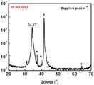
도 9a, 도 10a, 및 도 11a는 각각 아연 산화물 박막 제조예에 따른 단위 사이클을 수회 진행하여 얻은 4nm, 10nm, 및 30nm의 아연 산화물 박막들에 대한 XRD (X-Ray Diffraction) 그래프들이다.
도 9b, 도 10b, 및 도 11b는 각각 아연 산화물 박막 제조예에 따른 단위 사이클을 수회 진행하여 얻은 4nm, 10nm, 및 30nm의 아연 산화물 박막들에 대한 HR-TEM(High Resolution-Transmission Electron Microscopy) 이미지들과 회절패턴들을 보여준다.1A is a timing diagram of injection of a metal precursor gas, injection of a purge gas, and injection of a reactive gas for manufacturing a single crystal semiconductor layer according to an embodiment of the present invention.
1B is a timing diagram of injection of a metal precursor gas, injection of a purge gas, and injection of a reactive gas for manufacturing a single crystal semiconductor layer according to another embodiment of the present invention.
2 is a schematic diagram showing an apparatus for manufacturing a thin film according to an embodiment of the present invention.
3 is a cross-sectional view showing a structure according to an embodiment of the present invention.
4 is a cross-sectional view showing a thin film transistor according to an embodiment of the present invention.
5 is a cross-sectional view illustrating a light emitting diode according to an embodiment of the present invention.
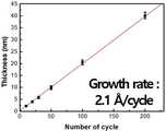
6 is a table summarizing parameters of a unit cycle for manufacturing a zinc oxide thin film according to the present preparation example.
7A is a graph showing the thickness of the zinc oxide thin film according to the number of unit cycles according to the zinc oxide thin film preparation example.
FIG. 7b shows an X-ray reflectivity (XRR) graph of a zinc oxide thin film obtained by performing a unit cycle several times according to a preparation example of a zinc oxide thin film.
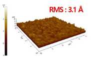
7c shows the AFM (Atomic Force Microscope) surface morphology of the zinc oxide thin film obtained by performing a unit cycle several times according to the preparation example of the zinc oxide thin film.
8A is a graph showing the thickness of the zinc oxide thin film according to the number of unit cycles according to Comparative Example of the zinc oxide thin film.
8B shows an XRR graph of a zinc oxide thin film obtained by performing a unit cycle several times according to a preparation example of a zinc oxide thin film.
8c shows the AFM surface morphology of the zinc oxide thin film obtained by performing a unit cycle several times according to Comparative Example of the zinc oxide thin film.
9A, 10A, and 11A are XRD (X-Ray Diffraction) graphs for zinc oxide thin films of 4 nm, 10 nm, and 30 nm obtained by performing a unit cycle several times according to the preparation example of the zinc oxide thin film, respectively.
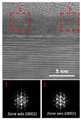
9b, 10b, and 11b are HR-TEM (High Resolution-Transmission Electron Microscopy) images of 4 nm, 10 nm, and 30 nm zinc oxide thin films obtained by performing unit cycles according to the zinc oxide thin film preparation example several times, respectively. fields and diffraction patterns.
이하, 본 발명을 보다 구체적으로 설명하기 위하여 본 발명에 따른 바람직한 실시예를 첨부된 도면을 참조하여 보다 상세하게 설명한다. 그러나, 본 발명은 여기서 설명되어지는 실시예에 한정되지 않고 다른 형태로 구체화될 수도 있다. 도면들에 있어서, 층이 다른 층 또는 기판 "상"에 있다고 언급되어지는 경우에 그것은 다른 층 또는 기판 상에 직접 형성될 수 있거나 또는 그들 사이에 제 3의 층이 개재될 수도 있다. 본 실시예들에서 "제1", "제2", 또는 "제3"는 구성요소들에 어떠한 한정을 가하려는 것은 아니며, 다만 구성요소들을 구별하기 위한 용어로서 이해되어야 할 것이다.Hereinafter, preferred embodiments according to the present invention will be described in more detail with reference to the accompanying drawings in order to describe the present invention in more detail. However, the present invention is not limited to the embodiments described herein and may be embodied in other forms. In the drawings, when a layer is said to be “on” another layer or substrate, it may be formed directly on the other layer or substrate, or a third layer may be interposed therebetween. In the present embodiments, "first", "second", or "third" is not intended to impose any limitation on the components, but should be understood as terms for distinguishing the components.
본 명세서에서 "Cx-Cy"라고 기재한 경우에는, 탄소수 x와 탄소수 y 사이의 모든 정수에 해당하는 수의 탄소수를 갖는 경우도 함께 기재된 것으로 해석되어야 한다.When described as "Cx-Cy" in the present specification, it should be construed as also described as having a number of carbon atoms corresponding to all integers between carbon number x and carbon number y.
도 1a는 본 발명의 일 실시예에 따른 단결정 반도체층의 제조를 위한 금속 전구체 가스 주입, 퍼지 가스 주입, 및 반응 가스 주입 타이밍도이다. 도 1b는 본 발명의 다른 실시예에 따른 단결정 반도체층의 제조를 위한 금속 전구체 가스 주입, 퍼지 가스 주입, 및 반응 가스 주입 타이밍도이다. 도 2는 본 발명의 일 실시예에 따른 박막 제조장치를 나타낸 개략도이다.1A is a timing diagram of injection of a metal precursor gas, injection of a purge gas, and injection of a reactive gas for manufacturing a single crystal semiconductor layer according to an embodiment of the present invention. 1B is a timing diagram of injection of a metal precursor gas, injection of a purge gas, and injection of a reactive gas for manufacturing a single crystal semiconductor layer according to another embodiment of the present invention. 2 is a schematic diagram showing an apparatus for manufacturing a thin film according to an embodiment of the present invention.
도 1a, 도 1b, 및 도 2를 참조하면, 가스 유입구(120) 및 가스 유출구(140)을 구비하는 챔버 (100) 내의 스테이지(102) 상에 기판(S)을 로딩할 수 있다. 상기 기판(S)은 단결정 기판으로 일 예로서, 육방정계 결정구조를 갖는 기판, 구체적으로는 c-면 단결정 기판일 수 있다. 일 예로서, 상기 기판(S)은 사파이어 기판, 더 구체적으로는 c-면 사파이어 기판일 수 있다.1A, 1B, and 2 , a substrate S may be loaded on a
상기 기판(S)를 로딩하기 전에, 상기 챔버(100)는 제어부(150)에 의해 증착 온도로 가열되고 유지될 수 있다. 증착 온도는 20 내지 250 ℃, 50 내지 200 ℃, 80 내지 150 ℃, 90 내지 100 ℃, 또는 95 내지 105 ℃일 수 있다. 가스 유출구(140)은 진공펌프에 연결되어 있을 수 있다.Before loading the substrate S, the
먼저, 가스 유입구(120)에 연결된 모든 가스 유입 밸브들(130, 132, 134)를 닫고 상기 가스 유출구(140)에 연결된 가스 유출 밸브(142)를 열어 챔버(100) 내부를 진공상태로 만들 수 있다. 이 후, 금속 전구체 가스 제어 밸브(130)을 열고 가스 유출 밸브(142)를 닫은 상태에서, 상기 금속 전구체 저장부(110)으로부터 금속 전구체 가스를 챔버(100) 내로 공급할 수 있다.First, by closing all the
금속 전구체는 아연 전구체 또는 13족 금속 전구체일 수 있다. 아연 전구체는 일 예로서, 다이(C1-C5알킬)아연일 수 있다. 다이(C1-C5알킬)아연은 다이에틸아연(diethyl zinc, DEZ)일 수 있다. 13족 금속 전구체는 일 예로서, 갈륨 전구체, 인듐 전구체, 혹은 알루미늄 전구체로, 트리(C1-C5알킬)금속(여기서, 금속은 13족 금속)일 수 있다. 갈륨 전구체는 일 예로서, 트리메틸갈륨(Trimethyl Gallium; Ga(CH3)3)(TMGa)일 수 있고, 인듐 전구체는 일 예로서, 트리메틸인듐(Trimethyl Indium; In(CH3)3)(TMIn)일 수 있고, 알루미늄 전구체는 일 예로서, 트리메틸알루미늄(Trimethyl aluminum; Al(CH3)3)(TMAl)일 수 있다.The metal precursor may be a zinc precursor or a Group 13 metal precursor. The zinc precursor may be, for example, di(C1 -C5 alkyl)zinc. The di(C1 -C5 alkyl)zinc may be diethyl zinc (DEZ). The Group 13 metal precursor is, for example, a gallium precursor, an indium precursor, or an aluminum precursor, and may be a tri(C1 -C5 alkyl) metal (herein, the metal is a Group 13 metal). The gallium precursor may be, as an example, trimethyl gallium (Ga(CH3 )3 )(TMGa), and the indium precursor may be, as an example, trimethyl indium (In(CH3 )3 )(TMIn). may be, and the aluminum precursor may be, for example, trimethyl aluminum (Al(CH3 )3 ) (TMAl).
금속 전구체 저장부(110) 내에 금속 전구체는 액체 또는 고체 상태로 저장될 수 있다. 상기 금속 전구체 저장부(110)는 금속 전구체의 열분해 온도 미만으로 가열되고 이에 따라 금속 전구체는 소정의 증기압으로 챔버(100) 내로 공급될 수 있다. 이 때, 공급되는 금속 전구체는 캐리어 가스 없이 공급될 수 있다. 상기 금속 전구체는 가스 유출 밸브(142)가 닫긴 상태에서 공급되므로, 상기 챔버(100) 내에 축적되면서 상기 챔버(100) 내의 압력을 증가시킬 수 있다. 상기 금속 전구체는 상기 챔버(100)의 압력이 반응압력(PM)에 이를 때까지 공급될 수 있다(금속 전구체 공급 단계, MD1). 반응압력 즉, 금속 전구체 가스의 압력은 수십 mTorr 내지 수 Torr의 범위, 구체적으로 100 mTorr 내지 5 Torr, 500 mTorr 내지 3 Torr, 또는 700 mTorr 내지 1.5 Torr일 수 있다.The metal precursor may be stored in a liquid or solid state in the metal
반응압력에 이르면 금속 전구체 가스 제어 밸브(130)를 닫고, 소정 시간 챔버를 밀폐시킬 수 있다(금속 전구체 노출 단계, ME1). 상기 금속 전구체 공급 단계(MD1)와 상기 금속 전구체 노출 단계(ME1)는 금속 전구체 가압 도징 단계로 불리울 수 있다. 다만, 금속 전구체 노출 단계(ME1)는 경우에 따라 생략될 수도 있다.When the reaction pressure is reached, the metal precursor
금속 전구체 가압 도징 단계 즉, 상기 금속 전구체 공급 단계(MD1)와 상기 금속 전구체 노출 단계(ME1)에서 금속 전구체 가스는 기판 혹은 기판 상에 기 형성된 층의 표면에 화학흡착(chemisorption) 및 자기포화반응(self-saturated reaction)에 의해 증착될 수 있다. 상기 금속 전구체 가스의 화학 흡착과 자기포화반응은 가압된 환경 구체적으로, 라미나 플로우 환경이 아닌 가압된 정체 환경(stagnant environment)에서 진행되므로, 상기 금속 전구체 가스의 기판 혹은 기판 상에 기 형성된 층의 표면에의 화학 흡착률 혹은 표면 커버리지가 크게 향상될 수 있다.In the metal precursor pressurized dosing step, that is, the metal precursor supply step (MD1 ) and the metal precursor exposure step (ME1 ), the metal precursor gas is subjected to chemisorption and self-saturation on the substrate or the surface of the layer previously formed on the substrate. It may be deposited by a self-saturated reaction. Since the chemical adsorption and self-saturation reaction of the metal precursor gas proceeds in a pressurized environment, specifically, in a pressurized stagnant environment, not in a lamina flow environment, the substrate of the metal precursor gas or a layer formed on the substrate The rate of chemisorption or surface coverage on the surface can be greatly improved.
이 후, 챔버를 퍼지시킬 수 있다(금속 전구체 퍼지 단계, MP1). 구체적으로, 퍼지 가스 제어 밸브(132)와 가스 유출 밸브(142)를 열어, 퍼지 가스 저장부(112) 내의 퍼지 가스를 챔버 내의 기판 표면 상으로 흘려보내 기판의 표면에 흡착되지 못한 과잉 금속 전구체 가스 및 금속 전구체 가스와 기판 표면 사이의 반응에 의해 생성된 반응 산물을 제거할 수 있다. 이 때, 퍼지 가스는 불활성 가스로 불활성 가스는 예를 들어, 아르곤(Ar), 질소(N2) 또는 이들의 조합인 가스를 구비할 수 있다.Thereafter, the chamber may be purged (metal precursor purge step, MP1 ). Specifically, the purge
상기 금속 전구체 가압 도징 단계 (MD1, ME1)와 금속 전구체 퍼지 단계(MP1)는 금속 전구체 서브 사이클(M-SC1)을 구성할 수 있고, 금속 전구체 서브 사이클(M-SCn)은 1회 내지 다수회, 구체적으로 1 내지 10회(n=1 ~ 10), 예를 들어 2 내지 7회(n=2~7), 또는 3 내지 5회 (n=3~5) 실시할 수 있다. 상기 다수의 금속 전구체 서브 사이클들(M-SCn)은 금속 전구체 단위 사이클(M-UC)을 구성할 수 있다. 상기 금속 전구체 서브 사이클들을 다수회 수행할 때(M-SC1, M-SC2, … M-SCn, n≥2), 도 1a에 도시된 것과 같은 실시예에서는 금속 전구체 가압 도징 단계들(MD1, MD2, … MDn, ME1, ME2, … MEn, n≥2)에서의 반응압력(PM)은 실질적으로 동일할 수 있고, 도 1b에 도시된 것과 같은 실시예에서는 금속 전구체 가압 도징 단계들(MD1, MD2, … MDn, ME1, ME2, … MEn, n≥2)에서의 반응압력(PM1, PM2, PM3)은 서로 다를 수 있다. 도 1b에서는 금속 전구체 가압 도징 단계들(MD1, MD2, … MDn, ME1, ME2, … MEn, n≥2)의 횟수가 증가할수록 반응압력(PM1, PM2, PM3)을 점차 증가시키는 것으로 도시하였으나, 이에 한정되지 않고 반응압력은 점차 감소할 수도 있다.The metal precursor pressurized dosing step (MD1 , ME1 ) and the metal precursor purge step (MP1 ) may constitute a metal precursor sub-cycle (M-SC1 ), and the metal precursor sub-cycle (M-SCn ) is 1 to many times, specifically 1 to 10 times (n = 1 to 10), for example, 2 to 7 times (n = 2 to 7), or 3 to 5 times (n = 3 to 5) can be performed have. The plurality of metal precursor subcycles M-SCn may constitute a metal precursor unit cycle M-UC. When performing the metal precursor sub-cycles multiple times (M-SC1 , M-SC2 , ... M-SCn , n≥2), in an embodiment such as that shown in FIG. 1A, the metal precursor pressurized dosing steps (The reaction pressures (P M ) at MD1 , MD2 , … MDn , ME1 , ME2 , … MEn, n≥2) may be substantially the same, and in an embodiment such as that shown in FIG. 1B , the metal precursor pressurizedThe reaction pressures P M1 , PM2 , PM3 in the dosing steps MD1 , MD2 , ... MDn , ME1 , ME2 , ... MEn, n≥2 may be different from each other. In FIG. 1b, as the number of metal precursor pressurized dosing steps (MD1 , MD2 , ... MDn , ME1, ME2, … MEn, n≥2) increases, the reaction pressure (PM1 , PM2 , PM3 ) is gradually increased. Although illustrated as increasing, the reaction pressure is not limited thereto and the reaction pressure may be gradually decreased.
금속 전구체 단위 사이클(M-UC) 수행후 후, 반응가스를 상기 챔버 내로 공급하는 반응가스 공급 단계(반응가스 공급 단계, OD1)를 수행할 수 있다. 상기 반응가스는 상기 기판 상에 흡착된 금속 전구체와 반응할 수 있다. 상기 반응가스는 구체적으로 상기 금속 전구체를 산화 또는 질화시켜 금속 산화물 단위층 혹은 금속 질화물 단위층을 형성하는 산화제 또는 질화제일 수 있다. 산화제는 H2O, H2O2, O2, 또는 O3일 수 있으나 이에 한정되는 것은 아니다. 일 구체예에서, 상기 산화제는 H2O일 수 있고, 질화제는 NH3일 수 있으나 이에 한정되는 것은 아니다. 금속 전구체로서 아연 전구체를 사용하는 경우에 반응가스로 산화제를 사용할 수 있고, 금속 전구체로서 13족 금속 전구체를 사용하는 경우에 반응가스로 질화제를 사용할 수 있다.After performing the metal precursor unit cycle (M-UC), a reaction gas supply step (reaction gas supply step, OD1 ) of supplying a reaction gas into the chamber may be performed. The reaction gas may react with the metal precursor adsorbed on the substrate. The reaction gas may be an oxidizing or nitriding agent that specifically oxidizes or nitridizes the metal precursor to form a metal oxide unit layer or a metal nitride unit layer. The oxidizing agent may be H2 O, H2 O2 , O2 , or O3 , but is not limited thereto. In one embodiment, the oxidizing agent may be H2 O, the nitriding agent may be NH3 , but is not limited thereto. When a zinc precursor is used as a metal precursor, an oxidizing agent may be used as a reaction gas, and when a Group 13 metal precursor is used as a metal precursor, a nitriding agent may be used as a reaction gas.
일 실시예에서, 반응가스 제어 밸브(134)을 열고 가스 유출 밸브(142)를 닫은 상태에서, 상기 반응가스 저장부(114)로부터 반응가스를 챔버(100) 내로 공급할 수 있다. 상기 반응가스는 가스 유출 밸브(142)가 닫긴 상태에서 공급되므로, 상기 챔버(100) 내에 축적되면서 상기 챔버(100) 내의 압력을 증가시킬 수 있다. 상기 반응가스는 상기 챔버(100)의 압력이 반응압력(POX)에 이를 때까지 공급될 수 있다. 반응압력 즉, 반응가스의 압력은 백 mTorr 내지 십 Torr의 범위, 구체적으로 200 mTorr 내지 8 Torr, 500 mTorr 내지 5 Torr, 또는 700 mTorr 내지 2 Torr 일 수 있다. 일 실시예에서, 공급되는 반응가스는 캐리어 가스없이 공급될 수 있다. 상기 반응가스가 H2O 또는 H2O2 인 경우, 반응가스 저장부(114) 내에 반응가스는 액체 상태로 저장될 수 있다. 상기 반응가스 저장부(114)는 가열되고 상기 반응가스는 소정의 증기압으로 챔버(100) 내로 공급될 수 있다In an embodiment, in a state in which the reaction
반응압력(POX)에 이르면 반응가스 제어 밸브(134)를 닫고, 소정 시간 챔버를 밀폐시킬 수 있다(반응가스 노출 단계, OE1). 상기 반응가스 공급 단계(OD1)와 상기 반응가스 노출 단계(OE1)는 반응가스 가압 도징 단계로 불리울 수 있다. 다만, 상기 반응가스 노출 단계(OE1)는 경우에 따라 생략될 수도 있다.When the reaction pressure POX is reached, the reaction
상기 반응가스 가압 도징 단계 즉, 상기 반응가스 공급 단계(OD1)와 상기 반응가스 노출 단계(OE1)에서 반응가스는 기판 상에 형성된 금속 전구체층과 반응하여 상기 금속 전구체층을 반도체 단위층 일 예로서, 금속 산화물 단위층 또는 금속 질화물 단위층으로 변화시킬 수 있다. 일 예로서, 금속 산화물 단위층은 아연 산화물 단위층일 수 있고, 금속 질화물 단위층은 갈륨 질화물 단위층일 수 있다. 앞서 설명한 바와 같이, 상기 반응가스와 상기 금속 전구체층과의 반응은 가압된 환경 구체적으로, 라미나 플로우 환경이 아닌 가압된 정체 환경(stagnant environment)에서 진행될 수 있다. 그러나, 이에 한정되지 않고 반응가스는 가스 유출 밸브(142)를 연 상태에서 공급되어 챔버 내에서 라미나 플로우를 형성한 상태에서 상기 금속 전구체층과 반응할 수도 있다.In the reaction gas pressurization dosing step, that is, the reaction gas supply step (OD1 ) and the reaction gas exposure step (OE1 ), the reaction gas reacts with the metal precursor layer formed on the substrate to form the metal precursor layer as a semiconductor unit layer. For example, it may be changed to a metal oxide unit layer or a metal nitride unit layer. As an example, the metal oxide unit layer may be a zinc oxide unit layer, and the metal nitride unit layer may be a gallium nitride unit layer. As described above, the reaction between the reaction gas and the metal precursor layer may be performed in a pressurized environment, specifically, in a pressurized stagnant environment rather than a lamina flow environment. However, the present invention is not limited thereto, and the reaction gas may be supplied while the
이 후, 챔버를 퍼지시킬 수 있다(반응가스 퍼지 단계, OP1). 구체적으로, 퍼지 가스 제어 밸브(132)와 가스 유출 밸브(142)를 열어, 퍼지 가스 저장부(112) 내의 퍼지 가스를 기판 표면 상으로 흘려보내 금속 전구체층과 반응하지 못한 과잉 반응가스 및 반응가스와 금속 전구체 사이의 반응에 의해 생성된 반응 산물을 제거할 수 있다. 이 때, 퍼지 가스는 불활성 가스로 불활성 가스는 예를 들어, 아르곤(Ar), 질소(N2) 또는 이들의 조합인 가스를 구비할 수 있다.Thereafter, the chamber may be purged (reactant gas purging step, OP1 ). Specifically, by opening the purge
상기 반응가스 가압 도징 단계 (OD1, OE1), 및 반응가스 퍼지 단계(OP1)는 반응가스 서브 사이클(O-SC1)을 구성할 수 있고, 반응가스 서브 사이클(O-SCn)은 1회 내지 다수회, 구체적으로 1 내지 10회(n=1 ~ 10), 예를 들어 2 내지 7회(n=2~7), 또는 3 내지 5회 (n=3~5) 실시할 수 있다. 상기 다수의 반응가스 서브 사이클들(O-SCn)은 반응가스 단위 사이클(O-UC)을 구성할 수 있다. 상기 반응가스 서브 사이클들을 다수회 수행할 때(O-SC1, O-SC2, … O-SCn, n≥2), 도 1a에 도시된 것과 같은 실시예에서는 반응가스 가압 도징 단계들(OD1, OD2, … ODn, OE1, OE2, … OEn, n≥2)에서의 반응압력(POX)은 실질적으로 동일할 수 있고, 도 1b에 도시된 것과 같은 실시예에서는 반응가스 가압 도징 단계들(OD1, OD2, … ODn, OE1, OE2, … OEn, n≥2)에서의 반응압력(POX1, POX2, POX3)은 서로 다를 수 있다. 도 1b에서는 반응가스 가압 도징 단계들(OD1, OD2, … ODn, OE1, OE2, … OEn, n≥2)의 횟수가 증가할수록 반응압력(POX1, POX2, POX3)을 점차 증가시키는 것으로 도시하였으나, 이에 한정되지 않고 반응압력은 점차 감소할 수도 있다.The reaction gas pressurized dosing step (OD1 , OE1 ), and the reaction gas purge step (OP1 ) may constitute a reaction gas sub-cycle (O-SC1 ), and the reaction gas sub-cycle (O-SCn ) is performed 1 to many times, specifically 1 to 10 times (n=1 to 10), for example 2 to 7 times (n=2 to 7), or 3 to 5 times (n=3 to 5) can The plurality of reactive gas sub-cycles O-SCn may constitute a reactive gas unit cycle O-UC. When performing the reaction gas sub-cycles a plurality of times (O-SC1 , O-SC2 , ... O-SCn , n≥2), in an embodiment such as that shown in FIG. 1A, the reaction gas pressurization dosing steps ( OD1 , OD2 , ... ODn , OE1 , OE2 , ... OEn , n ≥ 2), the reaction pressure (PO OX ) may be substantially the same, and in an embodiment such as that shown in FIG. 1B , The reaction pressures (POX1 , POX2 , POX3 ) in the reaction gas pressurized dosing steps (OD1 , OD2 , ... ODn , OE1 , OE2 , ... OEn , n≥2) may be different from each other . In FIG. 1b, as the number of reaction gas pressurization dosing steps (OD1 , OD2 , ... ODn , OE1 , OE2 , ... OEn , n≥2) increases, the reaction pressure (POX1 , POX2 , POX3 ) ) is shown to be gradually increased, but the present invention is not limited thereto, and the reaction pressure may be gradually decreased.
상기 금속 전구체 단위 사이클(M-UC) 1회와 상기 반응가스 단위 사이클(O-UC) 1회를 수행하였을 때, 얻어지는 상기 반도체 단위층의 두께 즉, 단위 사이클당 두께는 약 1.7 내지 3Å 구체적으로 1.9 내지 2.5 Å 또는 2 내지 2.3 Å일 수 있다. 이 후, 상기 금속 전구체 단위 사이클(M-UC)과 상기 반응가스 단위 사이클(O-UC)을 교호적으로 반복 수행할 수 있다. 반복 수행의 횟수는 반도체층의 최종 두께를 결정할 수 있다. 또한, 본 실시예에 따른 방법을 사용하여 얻어지는 반도체층은 표면 거칠기가 수 Å (RMS, Root Mean Square) 일 예로서, 3 Å 이하 나아가 2.5 Å 이하 일 예로서, 2 내지 2.5 Å의 매우 낮은 값을 나타내는 등 우수한 표면 몰폴러지를 나타낼 수 있다. 또한, 본 실시예에 따른 방법을 사용하여 얻어지는 반도체층은 그의 밀도가 5.1 g/㎝3 이상, 일 예로서 5.2 g/㎝3 또는 5.3 g/㎝3 이상 구체적으로, 5.2 g/㎝3 내지 5.5 g/㎝3으로 매우 치밀한 막특성을 나타낼 수 있다.When the metal precursor unit cycle (M-UC) and the reaction gas unit cycle (O-UC) are performed once, the thickness of the semiconductor unit layer obtained, that is, the thickness per unit cycle, is about 1.7 to 3 Å. Specifically, 1.9 to 2.5 Å or 2 to 2.3 Å. Thereafter, the metal precursor unit cycle (M-UC) and the reaction gas unit cycle (O-UC) may be alternately repeated. The number of repetitions may determine the final thickness of the semiconductor layer. In addition, the semiconductor layer obtained by using the method according to the present embodiment has a surface roughness of several Å (RMS, Root Mean Square), for example, 3 Å or less, and further 2.5 Å or less, for example, a very low value of 2 to 2.5 Å. It can exhibit excellent surface morphology, such as showing In addition, the semiconductor layer obtained by using the method according to the present embodiment has a density of 5.1 g/cm3 or more, for example, 5.2 g/cm3 or 5.3 g/cm3 or more, specifically, 5.2 g/cm3 to 5.5 In g/cm3 , very dense membrane properties can be exhibited.
이와 같이 형성된 반도체층은 적어도 반응압력을 높힌 가압된 정체 환경(stagnant environment)에서 금속 전구체 흡착이 진행되었기 때문에, 이는 일반 ALD법 즉, 가압된 환경이 아닌 라미나 플로우 환경에서 금속 전구체 흡착이 진행될 경우 얻어지는 약 1Å의 두께 대비 매우 큰 단위 사이클당 두께로 형성될 수 있고, 표면 거칠기가 낮으며, 또한 치밀한 막으로 형성될 수 있다.In the semiconductor layer formed in this way, since the metal precursor adsorption proceeded in a pressurized stagnant environment with at least an increased reaction pressure, this is a general ALD method, that is, when the metal precursor adsorption proceeds in a lamina flow environment rather than a pressurized environment. It can be formed to a thickness per unit cycle that is very large compared to the obtained thickness of about 1 Å, and has a low surface roughness and can be formed into a dense film.
본 실시예에 따른 방법을 사용하여 얻어지는 반도체층은 단결정 일 예로서, 육방정계 결정구조 구체적으로는 육방정계 우르짜이트(hexagonal wurtzite) 구조를 가질 수 있다. 또한, 상기 단결정 반도체층은 c-면 구체적으로는 (0002)면 우선배향성(preferred orientation)을 가질 수 있다. 다른 예에서, 상기 단결정 반도체층의 일부 영역은 m-면 구체적으로는 (1-100)면 우선배향성을 가질 수 있다. 구체적으로, 상기 단결정 반도체층은 성장되는 두께가 증가함에 따라 c-면 우선배향성에서 m-면 우선배향성을 갖는 막으로 변화될 수 있다. 다시 말해서, 상기 반도체층이 상기 단결정 기판과 인접하는 하부 영역은 c-면 우선배향성을 갖고, 상기 하부 영역의 상부에 위치한 영역은 m-면 우선배향성을 가질 수 있다. 일 예에서, 상기 단결정 반도체층이 아연 산화물층인 경우에 약 10nm 이하의 두께에서는 c-면 우선배향성을 갖고 10nm 이상의 두께에서는 m-면 우선배향성을 가질 수 있다.The semiconductor layer obtained by using the method according to the present embodiment is an example of a single crystal, and may have a hexagonal crystal structure, specifically, a hexagonal wurtzite structure. In addition, the single crystal semiconductor layer may have a preferred orientation of the c-plane, specifically (0002) plane. In another example, a partial region of the single crystal semiconductor layer may have a preferential orientation in the m-plane, specifically (1-100) plane. Specifically, the single crystal semiconductor layer may be changed from a c-plane preferential orientation to a film having an m-plane preferential orientation as the grown thickness increases. In other words, a lower region of the semiconductor layer adjacent to the single crystal substrate may have c-plane preferential orientation, and a region positioned above the lower region may have m-plane preferential orientation. In one example, when the single crystal semiconductor layer is a zinc oxide layer, it may have c-plane preferential orientation at a thickness of about 10 nm or less, and may have m-plane preferential orientation at a thickness of 10 nm or more.
도 3은 본 발명의 일 실시예에 따른 구조체를 나타낸 단면도이다.3 is a cross-sectional view showing a structure according to an embodiment of the present invention.
도 3을 참조하면, 기판(10)이 제공될 수 있다. 상기 기판(S)은 단결정 기판으로 일 예로서, 육방정계 결정구조를 갖는 기판, 구체적으로는 c-면 단결정 기판일 수 있다. 일 예로서, 상기 기판(S)은 사파이어 기판, 더 구체적으로는 c-면 사파이어 기판일 수 있다. 상기 기판(10)은 절연기판일 수 있다.Referring to FIG. 3 , a
상기 기판(10) 상에 단결정 반도체층(20)이 배치될 수 있다. 상기 단결정 반도체층(20)은 도 1a, 도 1b, 및 도 2를 참조하여 설명한 바와 같은 방법으로 상기 기판(10) 상에 에피택셜 성장된 에피택셜층(epitaxial layer)일 수 있다. 상기 단결정 반도체층(20)은 육방정계 결정구조 구체적으로는 육방정계 우르짜이트(hexagonal wurtzite) 구조를 가질 수 있다. 또한, 상기 단결정 반도체층은 c-면 구체적으로는 (0002)면 우선배향성(preferred orientation)을 가질 수 있다. 다른 예에서, 상기 단결정 반도체층(20)의 일부 영역은 m-면 구체적으로는 (1-100)면 우선배향성을 가질 수 있다. 구체적으로, 상기 단결정 반도체층(20)은 성장되는 두께가 증가함에 따라 c-면 우선배향성에서 m-면 우선배향성을 갖는 막으로 변화될 수 있다. 다시 말해서, 상기 반도체층(20)이 상기 단결정 기판과 인접하는 하부 영역은 c-면 우선배향성을 갖고, 상기 하부 영역의 상부에 위치한 영역은 m-면 우선배향성을 가질 수 있다. 일 예에서, 상기 단결정 반도체층(20)이 아연 산화물층인 경우에 약 10nm 이하의 두께에서는 c-면 우선배향성을 갖고 10nm 이상의 두께에서는 m-면 우선배향성을 가질 수 있다. 단결정 반도체층(20)은 1 내지 1000nm, 일 예로서 2 내지 100nm, 구체적으로는 3 내지 50nm의 두께를 가질 수 있다.A single
도 4는 본 발명의 일 실시예에 따른 박막트랜지스터를 나타낸 단면도이다.4 is a cross-sectional view showing a thin film transistor according to an embodiment of the present invention.
도 4를 참조하면, 도 3를 참조하여 설명한 단결정 반도체층(20)을 포토리소그래피 등을 사용하여 패터닝한 후, 패터닝된 단결정 반도체층(20) 상에 게이트 절연막(30)을 형성할 수 있다. 상기 게이트 절연막(30)은 실리콘 산화막, 실리콘 산질화막, 알루미늄 산화막, 알루미늄 산질화막, 또는 이들의 복합막일 수 있다. 상기 게이트 절연막(30)은 원자층 증착법을 사용하여 형성할 수 있으며, 일 예로서 알루미늄 산화막일 수 있다. 상기 게이트 절연막(30) 상에 상기 단결정 반도체층(20)에 중첩하는 게이트 전극(40)을 형성할 수 있다. 상기 게이트 전극(40)은 Al, Cr, Cu, Ta, Ti, Mo, W, 또는 이들의 합금을 사용하여 형성할 수 있다. 상기 게이트 전극(40) 상에 층간절연막(35)을 형성한 후, 상기 층간절연막(35) 내에 상기 패터닝된 단결정 반도체층(20)의 양측 단부들을 각각 노출시키는 콘택홀들을 형성한 후, 상기 콘택홀들 내에 소오스/드레인 전극들(50S, 50D)을 형성할 수 있다. 상기 소오스 전극(S)과 드레인 전극(D)은 알루미늄(Al), 네오디뮴(Nd), 은(Ag), 크롬(Cr), 티타늄(Ti), 탄탈륨(Ta) 및 몰리브덴(Mo) 중 적어도 어느 하나의 금속 또는 이들을 포함하는 합금, 또는 금속산화물 전도성막 일 예로서, ITO(Indium Tin Oxide)을 사용하여 형성할 수 있다.Referring to FIG. 4 , after the single
이와 같이, 단결정 반도체층(20)을 채널층으로 구비하는 박막트랜지스터는 우수한 전자이동도를 나타낼 수 있다.As described above, the thin film transistor including the single
도 5는 본 발명의 일 실시예에 따른 발광다이오드를 나타낸 단면도이다.5 is a cross-sectional view illustrating a light emitting diode according to an embodiment of the present invention.
도 5를 참조하면, 도 3을 참조하여 설명한 단결정 반도체층(20)이 형성된 기판(10)을 제공할 수 있다. 이 때, 단결정 반도체층(20)은 버퍼층(20)으로 명명할 수도 있다. 도 3을 참조하여 설명한 바와 같이, 상기 버퍼층(20)은 최상부면이 c-면 우선배향성을 가질 수도 있고 혹은 m-면 우선배향성을 가질 수도 있다.Referring to FIG. 5 , the
상기 버퍼층(20) 상에 발광구조체층(60)을 형성할 수 있다. 상기 발광구조체층(60)은 차례로 적층된 제1 도전형 반도체층(61) 및 제2 도전형 반도체층(63)을 구비할 수 있다. 나아가, 상기 발광구조체층(60)은 상기 제1 도전형 반도체층(61)과 상기 제2 도전형 반도체층(63) 사이에 활성층(62)을 더 구비할 수도 있다.A light emitting
상기 제1 도전형 반도체층(61)은 산화물계 반도체층 일 예로서 ZnO층이거나 또는 질화물계 반도체층 일 예로서 InxAlyGa1-x-yN(0≤x≤1, 0≤y≤1, 0≤x+y≤1)층일 수 있다. 상기 제1 도전형 반도체층(61)은 n형 도펀트가 도핑되거나 혹은 도펀트 도핑되지 않은 상태에서도 n형을 나타내는 층일 수 있다. 질화물계 반도체층인 경우 n형 도펀트는 Si일 수 있다.The first conductivity
상기 제2 도전형 반도체층(63)은 산화물계 반도체층 일 예로서 ZnO층이거나 또는 질화물계 반도체층 일 예로서 InxAlyGa1-x-yN(0≤x≤1, 0≤y≤1, 0≤x+y≤1)층일 수 있다. 상기 제2 도전형 반도체층(63)은 p형 도펀트가 도핑된 층일 수 있다. 상기 제2 도전형 반도체층(63)이 질화물계 반도체층인 경우 p형 도펀트는 Mg일 수 있다. 상기 제2 도전형 반도체층(63)이 ZnO층인 경우 p형 도펀트는 Sb일 수 있다.The second conductivity
상기 활성층(62)은 단일 양자 우물 구조 혹은 다중 양자 우물 구조(multi-quantum well; MQW)를 가질 수 있다. 일 예로서, 상기 활성층(62)은 InGaN/GaN, AlGaN/(In)GaN, 또는 InAlGaN/(In)GaN의 다층구조인 다중 양자 우물 구조를 가질 수 있다. 다른 예로서, 상기 활성층(62)은 ZnO/ZnMgO의 다층구조인 다중 양자 우물 구조를 가질 수 있다.The
상기 발광 구조체층(60)는, 상기 버퍼층(20)을 도 1a, 도 1b, 및 도 2를 참조하여 설명한 가압식 원자층 증착법을 사용하여 형성한 것과는 달리, 금속 유기 화학 증착법(Metal Organic Chemical Vapor Deposition; MOCVD), 화학 기상 증착법(Chemical Vapor Deposition; CVD), 플라즈마 화학 기상 증착법(Plasma-Enhanced Chemical Vapor Deposition; PECVD), 분자선 성장법(Molecular Beam Epitaxy; MBE), 수소화물 기상 성장법(Hydride Vapor Phase Epitaxy; HVPE) 등을 포함한 다양한 증착 또는 성장 방법을 이용하여 상기 버퍼층(20) 상에 에피택시얼하게 형성될 수 있다.The light emitting
이 때, 상기 버퍼층(20)의 최상부면이 c-면 우선배향성을 갖는 경우 상기 발광 구조체층(60) 또한 c-면 우선배향성을 갖도록 형성될 수 있고, 상기 버퍼층(20)의 최상부면이 m-면 우선배향성을 갖는 경우 상기 발광 구조체층(60) 또한 m-면 우선배향성을 갖도록 형성될 수 있다. 상기 발광 구조체층(60)이 c-면 우선배향성을 갖도록 성장된 경우, 이종원자 일 예로서 Ga원자와 N원자가 c축 방향에서 상부와 하부에 위치하므로 자발분극(spontaneous polarization)을 나타냄에 따라 정전기 장(electrostatic field)이 생성되고 이로 인해 전자와 정공의 분포가 왜곡되어 양자효율의 향상에 제한이 있을 수 있다. 이와는 달리, 상기 발광 구조체층(60)이 m-면 우선배향성을 갖도록 성장된 경우, 분극이 거의 존재하지 않아 양자효율이 크게 향상될 수 있다.At this time, when the uppermost surface of the
이 후, 상기 발광구조체층(60)의 일부 영역을 메사 식각하여 메사 영역 측부에 제1 도전형 반도체층(61)을 노출시킬 수 있다. 노출된 제1 도전형 반도체층(61) 및 상기 메사 영역 상부의 제2 도전형 반도체층(63)에 각각 접속하는 제1 전극(71) 및 제2 전극(72)을 형성할 수 있다.Thereafter, a portion of the light emitting
이하, 본 발명의 이해를 돕기 위하여 바람직한 실험예(example)를 제시한다. 다만, 하기의 실험예는 본 발명의 이해를 돕기 위한 것일 뿐, 본 발명이 하기의 실험예에 의해 한정되는 것은 아니다.Hereinafter, a preferred experimental example (example) is presented to help the understanding of the present invention. However, the following experimental examples are only for helping understanding of the present invention, and the present invention is not limited by the following experimental examples.
아연 산화물 박막 제조예Example of Zinc Oxide Thin Film Preparation
도 6은 본 제조예에 따른 아연 산화물 박막 제조를 위한 단위 사이클의 파라미터들을 정리하여 나타낸 표이다.6 is a table summarizing parameters of a unit cycle for manufacturing a zinc oxide thin film according to the present preparation example.
가스 유입구와 가스 유출구를 구비하는 챔버 내에 사파이어 기판을 로딩하고, 챔버를 100 ℃로 가열하였다. 가스 유출구를 닫은 상태에서, 상기 가스 유입구를 통해 상기 기판 상에 아연 전구체인 DEZ(diethylzinc)를 공급하였다(금속 전구체 공급 단계). 이 때, 상기 아연 전구체는 캐리어 가스 없이 공급되고, 챔버 내의 압력이 1 Torr에 이를 때까지 공급하였다. 이 후, 챔버 유입구도 닫아 챔버 압력을 1 Torr로 유지한 상태에서 상기 기판 표면 상에 상기 아연 전구체를 3초간 반응시켰다(금속 전구체 노출 단계). 이 후, 가스 유입구와 가스 유출구를 모두 연 상태에서 가스 유입구로 퍼지 가스인 아르곤을 15초간 공급하여 반응부산물 및 잔여반응가스를 퍼지하였다(금속 전구체 퍼지 단계). 상기 아연 전구체 공급 단계, 상기 아연 전구체 노출 단계, 및 상기 아연 전구체 퍼지 단계는 아연 전구체 서브 사이클을 구성하고, 상기 아연 전구체 서브 사이클을 4회 반복 수행하여 아연 원자층을 형성하였다.A sapphire substrate was loaded into a chamber having a gas inlet and a gas outlet, and the chamber was heated to 100°C. In a state in which the gas outlet was closed, DEZ (diethylzinc), a zinc precursor, was supplied on the substrate through the gas inlet (metal precursor supply step). At this time, the zinc precursor was supplied without a carrier gas, and was supplied until the pressure in the chamber reached 1 Torr. Thereafter, the zinc precursor was reacted on the substrate surface for 3 seconds while the chamber inlet was also closed and the chamber pressure was maintained at 1 Torr (metal precursor exposure step). Thereafter, argon as a purge gas was supplied to the gas inlet for 15 seconds while both the gas inlet and the gas outlet were opened to purify the reaction byproducts and the residual reaction gas (metal precursor purge step). The zinc precursor supply step, the zinc precursor exposure step, and the zinc precursor purge step constitute a zinc precursor subcycle, and the zinc precursor subcycle was repeated four times to form a zinc atomic layer.
이 후, 가스 유출구를 닫은 상태에서, 상기 가스 유입구를 통해 상기 아연 원자층 상에 반응가스인 H2O를 공급하였다. 이 때, 상기 반응가스는 캐리어 가스 없이 공급되고, 챔버 내의 압력이 1 Torr에 이를 때까지 공급하였다(반응가스 공급 단계). 이 후, 챔버 유입구도 닫아 챔버 압력을 1 Torr로 유지한 상태에서 상기 아연 원자층 표면 상에 H2O를 3초간 반응시켰다(반응가스 노출 단계). 이 후, 가스 유입구와 가스 유출구를 모두 연 상태에서 가스 유입구로 퍼지 가스인 아르곤을 25초간 공급하여 반응부산물 및 잔여반응가스를 퍼지하였다(반응가스 퍼지 단계). 상기 반응가스 공급 단계, 상기 반응가스 노출 단계, 및 상기 반응가스 퍼지 단계는 반응가스 서브 사이클을 구성하고, 상기 반응가스 서브 사이클을 4회 반복 수행하여 상기 아연 원자층 상에 산소 원자층을 형성하였다. 이에 따라 아연 산화물 단위층이 형성되었다. 상기 4회의 아연 전구체 서브 사이클들과 상기 4회의 반응가스 서브 사이클들은 아연 산화물 박막 제조를 위한 단위 사이클을 구성한다.Thereafter, in a state in which the gas outlet was closed, H2 O as a reaction gas was supplied on the zinc atomic layer through the gas inlet. At this time, the reaction gas was supplied without a carrier gas, and was supplied until the pressure in the chamber reached 1 Torr (reaction gas supply step).Thereafter, H 2 O was reacted on the surface of the zinc atomic layer for 3 seconds while maintaining the chamber pressure at 1 Torr by closing the chamber inlet (reaction gas exposure step). Thereafter, argon, which is a purge gas, was supplied to the gas inlet for 25 seconds while both the gas inlet and the gas outlet were opened to purify the reaction byproducts and residual reaction gas (reaction gas purge step). The reaction gas supply step, the reaction gas exposure step, and the reaction gas purge step constitute a reaction gas subcycle, and the reaction gas subcycle was repeated four times to form an atomic oxygen layer on the zinc atomic layer. . Accordingly, a zinc oxide unit layer was formed. The four sub-cycles of the zinc precursor and the four sub-cycles of the reaction gas constitute a unit cycle for manufacturing the zinc oxide thin film.
아연 산화물 박막 비교예Comparative Example of Zinc Oxide Thin Film
가스 유입구와 가스 유출구를 구비하는 챔버 내에 사파이어 기판을 로딩하고, 챔버를 100 ℃로 가열하였다. 아연 전구체인 DEZ와 캐리어 가스인 아르곤의 혼합가스를 2초간 공급하되, 챔버의 가스 유출구를 연 상태에서 공급하여 상기 DEZ 및 아르곤 혼합 가스가 챔버 내에서 라미나 플로우 상태를 유지하도록 하였다. 이 때 DEZ의 분압은 20 mTorr였다. 그 후, 퍼지 가스인 아르곤을 20초간 공급하여 반응부산물 및 잔여반응가스를 퍼지하고, 반응가스인 H2O와 캐리어 가스인 아르곤의 혼합가스를 2초간 라미타 플로우 상태를 유지하면서 공급하되 이 때, H2O의 분압은 20 mTorr였다. 그 후, 퍼지 가스인 아르곤을 40초간 공급하여 반응부산물 및 잔여반응가스를 퍼지하였다.A sapphire substrate was loaded into a chamber having a gas inlet and a gas outlet, and the chamber was heated to 100°C. A mixed gas of DEZ, which is a zinc precursor, and argon, which is a carrier gas, was supplied for 2 seconds, but the gas outlet of the chamber was supplied while the gas outlet was opened so that the DEZ and argon mixed gas maintained a lamina flow state in the chamber. At this time, the partial pressure of the DEZ was 20 mTorr. After that, argon, which is a purge gas, is supplied for 20 seconds to purge the reaction by-products and residual reaction gas, and a mixed gas of H2 O as a reaction gas and argon as a carrier gas is supplied while maintaining the Lamita flow state for 2 seconds, but at this time ,the partial pressure of H 2 O was 20 mTorr. Thereafter, argon as a purge gas was supplied for 40 seconds to purify the reaction by-products and the remaining reaction gas.
도 7a는 아연 산화물 박막 제조예에 따른 단위 사이클을 진행한 횟수에 따른 아연 산화물 박막의 두께를 보여주는 그래프이다. 도 8a는 아연 산화물 박막 비교예에 따른 단위 사이클을 진행한 횟수에 따른 아연 산화물 박막의 두께를 보여주는 그래프이다.7A is a graph showing the thickness of the zinc oxide thin film according to the number of unit cycles according to the zinc oxide thin film preparation example. 8A is a graph showing the thickness of the zinc oxide thin film according to the number of unit cycles according to Comparative Example of the zinc oxide thin film.
도 7a 및 도 8a를 참조하면, 아연 산화물 박막 제조예에 따른 단위 사이클 당 아연 산화물은 약 2.1Å의 두께로 형성되고, 아연 산화물 박막 비교예에 따른 단위 사이클 당 아연 산화물은 약 1.5Å의 두께로 형성되는 것을 알 수 있다. 이로부터, 아연 산화물 박막 제조예에 따른 단위 사이클 당 얻어지는 아연 산화물의 두께가 더 큰 것을 알 수 있다.Referring to FIGS. 7A and 8A , the zinc oxide per unit cycle according to the preparation example of the zinc oxide thin film is formed to a thickness of about 2.1 Å, and the zinc oxide per unit cycle according to the comparative example of the zinc oxide thin film has a thickness of about 1.5 Å. formation can be seen. From this, it can be seen that the thickness of the zinc oxide obtained per unit cycle according to the preparation example of the zinc oxide thin film is larger.
도 7b는 아연 산화물 박막 제조예에 따른 단위 사이클을 수회 진행하여 얻은 아연 산화물 박막의 XRR (X-ray reflectivity) 그래프를 나타낸다. 도 8b는 아연 산화물 박막 제조예에 따른 단위 사이클을 수회 진행하여 얻은 아연 산화물 박막의 XRR 그래프를 나타낸다. 여기서, 아연 산화물 박막 제조예에 따른 아연 산화물 박막과 아연 산화물 박막 비교예에 따른 아연 산화물 박막은 모두 약 15nm의 두께를 가지도록 형성하였다.FIG. 7b shows an X-ray reflectivity (XRR) graph of a zinc oxide thin film obtained by performing a unit cycle several times according to a preparation example of a zinc oxide thin film. 8B shows an XRR graph of a zinc oxide thin film obtained by performing a unit cycle several times according to a preparation example of a zinc oxide thin film. Here, both the zinc oxide thin film according to the zinc oxide thin film preparation example and the zinc oxide thin film according to the comparative example of the zinc oxide thin film were formed to have a thickness of about 15 nm.
도 7b 및 도 8b를 참조하면, 아연 산화물 박막 제조예에 따른 아연 산화물 박막은 약 5.304 g/cm3의 밀도로 형성되고, 아연 산화물 박막 비교예에 따른 아연 산화물 박막은 약 5.096 g/cm3의 밀도로 형성되는 것을 알 수 있다. 이로부터, 아연 산화물 박막 제조예에 따른 아연 산화물 박막의 밀도가 더 큰 것을 알 수 있다.7b and 8b, the zinc oxide thin film according to the preparation example of the zinc oxide thin film isformed at a density of about 5.304 g/cm 3 , and the zinc oxide thin film according to the comparative example of the zinc oxide thin film has a density of about 5.096 g/cm3 It can be seen that the density is formed. From this, it can be seen that the density of the zinc oxide thin film according to the preparation example of the zinc oxide thin film is higher.
도 7c는 아연 산화물 박막 제조예에 따른 단위 사이클을 수회 진행하여 얻은 아연 산화물 박막의 AFM(Atomic Force Microscope) 표면 몰폴로지를 나타낸다. 도 8c는 아연 산화물 박막 비교예에 따른 단위 사이클을 수회 진행하여 얻은 아연 산화물 박막의 AFM 표면 몰폴로지를 나타낸다. 여기서, 아연 산화물 박막 제조예에 따른 아연 산화물 박막과 아연 산화물 박막 비교예에 따른 아연 산화물 박막은 모두 약 20nm의 두께를 가지도록 형성하였다.7c shows the AFM (Atomic Force Microscope) surface morphology of the zinc oxide thin film obtained by performing a unit cycle several times according to the preparation example of the zinc oxide thin film. 8c shows the AFM surface morphology of the zinc oxide thin film obtained by performing a unit cycle several times according to Comparative Example of the zinc oxide thin film. Here, both the zinc oxide thin film according to the zinc oxide thin film Preparation Example and the zinc oxide thin film according to the comparative example of the zinc oxide thin film were formed to have a thickness of about 20 nm.
도 7c 및 도 8c를 참조하면, 아연 산화물 박막 제조예에 따른 아연 산화물 박막은 약 2.4 Å의 RMS (root mean square roughness)를 나타내고, 아연 산화물 박막 비교예에 따른 아연 산화물 박막은 약 3.1 Å의 RMS를 나타낸다. 이로부터, 아연 산화물 박막 제조예에 따른 아연 산화물 박막의 표면은 매우 낮은 거칠기를 갖는 것을 알 수 있다.Referring to FIGS. 7C and 8C , the zinc oxide thin film according to the preparation example of the zinc oxide thin film exhibits a root mean square roughness (RMS) of about 2.4 Å, and the zinc oxide thin film according to the comparative example of the zinc oxide thin film has an RMS of about 3.1 Å. indicates From this, it can be seen that the surface of the zinc oxide thin film according to the preparation example of the zinc oxide thin film has a very low roughness.
도 9a, 도 10a, 및 도 11a는 각각 아연 산화물 박막 제조예에 따른 단위 사이클을 수회 진행하여 얻은 4nm, 10nm, 및 30nm의 아연 산화물 박막들에 대한 XRD (X-Ray Diffraction) 그래프들이다. 도 9b, 도 10b, 및 도 11b는 각각 아연 산화물 박막 제조예에 따른 단위 사이클을 수회 진행하여 얻은 4nm, 10nm, 및 30nm의 아연 산화물 박막들에 대한 HR-TEM(High Resolution-Transmission Electron Microscopy) 이미지들과 회절패턴들을 보여준다. 도 9b, 도 10b, 및 도 11b에서 회절 패턴들 각각은 동일 도면 내 TEM 이미지에서 표시된 영역의 회절 패턴이다.9A, 10A, and 11A are XRD (X-Ray Diffraction) graphs for zinc oxide thin films of 4 nm, 10 nm, and 30 nm obtained by performing unit cycles according to the zinc oxide thin film preparation example several times, respectively. 9b, 10b, and 11b are HR-TEM (High Resolution-Transmission Electron Microscopy) images of zinc oxide thin films of 4 nm, 10 nm, and 30 nm obtained by performing a unit cycle several times according to the preparation example of the zinc oxide thin film, respectively. fields and diffraction patterns. Each of the diffraction patterns in FIGS. 9B, 10B, and 11B is a diffraction pattern of a region indicated in the TEM image in the same figure.
도 9a, 도 10a, 및 도 11a를 참조하면, 4nm의 아연 산화물 박막은 피크 중심이 35.05°에 위치하고, 2.2°의 반치폭을 갖는 피크를 제공하고, 10nm의 아연 산화물 박막은 피크 중심이 34.42°에 위치하고 0.79°의 반치폭을 갖는 피크와 피크 중심이 35.6°에 위치하는 피크가 병합된 피크를 제공하고, 30nm의 아연 산화물 박막은 피크 중심이 34.47°에 위치하고, 0.42°의 반치폭을 갖는 피크를 제공한다. 이로부터, 아연 산화물 박막 제조예에 따른 아연 산화물 박막은 매우 우수한 결정성을 갖는 것을 알 수 있다.9A, 10A, and 11A, the 4 nm zinc oxide thin film has a peak center located at 35.05° and provides a peak with a half width of 2.2°, and the 10 nm zinc oxide thin film has a peak center at 34.42°. A peak with a half maximum width of 0.79° and a peak with a peak center at 35.6° provide a merged peak, and a 30 nm zinc oxide thin film provides a peak with a peak center at 34.47° and a half width of 0.42° . From this, it can be seen that the zinc oxide thin film according to the preparation example of the zinc oxide thin film has very good crystallinity.
도 9b, 도 10b, 및 도 11b를 참조하면, HR-TEM 이미지에서 결정구조들이 확인되는 것으로 보아 아연 산화물 박막은 결정질 박막으로 형성된 것을 알 수 있다.Referring to FIGS. 9b, 10b, and 11b, it can be seen that the zinc oxide thin film is formed as a crystalline thin film, as crystal structures are confirmed in the HR-TEM image.
도 9b, 도 10b를 다시 참조하면, 회절패턴들에서 (0002)면들이 확인되는 것으로 보아, 10 nm 이하의 두께를 갖는 아연 산화물 박막은 [0002] 방향으로 결정이 우선배향된 것을 알 수 있다.Referring back to FIGS. 9b and 10b, as (0002) planes are confirmed in the diffraction patterns, it can be seen that in the zinc oxide thin film having a thickness of 10 nm or less, the crystals are preferentially oriented in the [0002] direction.
도 11b를 다시 참조하면, 기판 표면으로부터의 두께가 10 nm 이하인 영역의 회절패턴(1)에서 (0002)면(c-plane)만 관찰되고, 10 nm 초과인 영역의 회절패턴(2)에서 (0002)면과 더불어 (1-100)면(m-plane)이 관찰되고, 20 nm 이상인 영역의 회절패턴(3)에서 (1-100)면만 관찰되었다. 이러한 결과로부터, 상기 아연 산화물 반도체층은 성장되는 두께가 증가함에 따라 c-면 우선배향성을 갖는 막에서 m-면 우선배향성을 갖는 막으로 변화되는 것을 알 수 있다.Referring back to FIG. 11B, only the (0002) plane (c-plane) is observed in the
이상, 본 발명을 바람직한 실시예를 들어 상세하게 설명하였으나, 본 발명은 상기 실시예에 한정되지 않고, 본 발명의 기술적 사상 및 범위 내에서 당 분야에서 통상의 지식을 가진 자에 의하여 여러가지 변형 및 변경이 가능하다.Above, the present invention has been described in detail with reference to preferred embodiments, but the present invention is not limited to the above embodiments, and various modifications and changes by those skilled in the art within the technical spirit and scope of the present invention This is possible.
Claims (18)
Translated fromKorean상기 금속 전구체 가압 도징 단계 후, 상기 챔버를 퍼지하는 금속 전구체 퍼지 단계;
상기 금속 전구체 퍼지 단계 후, 반응가스를 상기 챔버 내로 공급하여 상기 기판 상에 흡착된 금속 전구체와 반응시키는 반응가스 공급 단계; 및
상기 반응가스 공급 단계 후, 상기 챔버를 퍼지하는 반응가스 퍼지 단계를 포함하는 단위 사이클을 다수회 진행하여,
상기 단결정 기판 상에 단결정 반도체층을 형성하되,
상기 단결정 기판은 육방정계 결정구조를 갖는 기판이고,
상기 단결정 반도체층은 육방정계 우르짜이트(hexagonal wurtzite) 구조를 갖는 반도체층인 단결정 반도체층 제조방법.A metal precursor pressurized dosing step of supplying a metal precursor to the single crystal substrate in a state in which the outlet of the chamber into which the single crystal substrate is closed is closed, thereby increasing a reaction pressure in the chamber to adsorb the metal precursor on the surface of the substrate;
a metal precursor purging step of purging the chamber after the metal precursor pressurized dosing step;
after the metal precursor purge step, a reaction gas supply step of supplying a reaction gas into the chamber to react with the metal precursor adsorbed on the substrate; and
After the reaction gas supply step, a unit cycle including a reaction gas purge step of purging the chamber is performed a plurality of times,
A single crystal semiconductor layer is formed on the single crystal substrate,
The single crystal substrate is a substrate having a hexagonal crystal structure,
The single crystal semiconductor layer is a semiconductor layer having a hexagonal wurtzite structure.
상기 단결정 반도체층은 c-면 우선배향성을 갖는 반도체층인 단결정 반도체층 제조방법.The method according to claim 1,
The single crystal semiconductor layer is a semiconductor layer having a c-plane preferential orientation.
상기 단결정 기판은 c-면 기판이고,
상기 단결정 반도체층의 일부 영역은 m-면 우선배향성을 갖는 단결정 반도체층 제조방법.The method according to claim 1,
The single crystal substrate is a c-plane substrate,
A method of manufacturing a single crystal semiconductor layer in which a partial region of the single crystal semiconductor layer has an m-plane preferential orientation.
상기 단결정 반도체층이 상기 단결정 기판과 인접하는 하부 영역은 c-면 우선배향성을 갖고, 상기 하부 영역의 상부에 위치한 영역은 m-면 우선배향성을 갖는 단결정 반도체층 제조방법.5. The method according to claim 4,
A lower region of the single-crystal semiconductor layer adjacent to the single-crystal substrate has c-plane preferential orientation, and an upper region of the lower region has m-plane preferential orientation.
상기 금속 전구체는 아연 전구체이고,
상기 반응가스는 산화제이고,
상기 단결정 반도체층은 ZnO층인 단결정 반도체층 제조방법.The method according to claim 1,
The metal precursor is a zinc precursor,
The reaction gas is an oxidizing agent,
The single crystal semiconductor layer is a method of manufacturing a single crystal semiconductor layer is a ZnO layer.
상기 금속 전구체는 III족 금속 전구체이고,
상기 반응가스는 질화제이고,
상기 단결정 반도체층은 III족 금속 질화물층인 단결정 반도체층 제조방법.The method according to claim 1,
The metal precursor is a Group III metal precursor,
The reaction gas is a nitriding agent,
The method of manufacturing a single crystal semiconductor layer, wherein the single crystal semiconductor layer is a group III metal nitride layer.
상기 금속 전구체 가압 도징 단계와 상기 금속 전구체 퍼지 단계는 금속 전구체 서브 사이클을 구성하고,
상기 반응가스 공급 단계 전에, 상기 금속 전구체 서브 사이클을 다수회 수행하는 단결정 반도체층 제조방법.The method according to claim 1,
The metal precursor pressurized dosing step and the metal precursor purge step constitute a metal precursor subcycle,
Before the step of supplying the reaction gas, a method of manufacturing a single crystal semiconductor layer for performing the metal precursor sub-cycle a plurality of times.
상기 반응가스 공급단계는
상기 챔버의 유출구를 닫은 상태에서 상기 반응가스를 공급하여 상기 챔버 내 반응압력을 증가시킨 상태에서 진행하는 반응가스 가압 도징(dosing) 단계로 진행하는 단결정 반도체층 제조방법.The method according to claim 1,
The reaction gas supply step is
A method of manufacturing a single crystal semiconductor layer that proceeds to a reaction gas pressurized dosing step in which the reaction pressure in the chamber is increased by supplying the reaction gas in a state in which the outlet of the chamber is closed.
상기 반응가스 가압 도징 단계와 상기 반응가스 퍼지 단계는 반응가스 서브 사이클을 구성하고,
상기 단위 사이클은 상기 반응가스 서브 사이클을 연속하여 다수회 수행하는 것을 포함하는 단결정 반도체층 제조방법.10. The method of claim 9,
The reaction gas pressure dosing step and the reaction gas purge step constitute a reaction gas subcycle,
wherein the unit cycle includes continuously performing the reaction gas subcycle a plurality of times.
상기 챔버의 온도는 80 내지 150 ℃의 범위 내에 있는 단결정 반도체층 제조방법.The method according to claim 1,
The temperature of the chamber is within the range of 80 to 150 ℃ single crystal semiconductor layer manufacturing method.
상기 채널층은, 청구항 1, 청구항 3 내지 청구항 11 중 어느 한 항의 방법을 사용하여 형성한 단결정 반도체층인 박막트랜지스터 제조방법.A method for manufacturing a thin film transistor having a gate electrode, a gate insulating film, a channel layer, and source and drain electrodes, the method comprising:
The method for manufacturing a thin film transistor, wherein the channel layer is a single crystal semiconductor layer formed using the method of any one of claims 1 and 3 to 11.
상기 버퍼층은, 청구항 1, 청구항 3 내지 청구항 11 중 어느 한 항의 방법을 사용하여 형성한 단결정 반도체층인 발광다이오드 제조방법.a buffer layer, a light emitting structure layer having a first conductivity type semiconductor layer and a second conductivity type semiconductor layer stacked on the buffer layer, a first electrode connected to the first conductivity type semiconductor layer, and the second conductivity type semiconductor layer In the light emitting diode manufacturing method having a second electrode to be connected,
The method for manufacturing a light emitting diode, wherein the buffer layer is a single crystal semiconductor layer formed using the method of any one of claims 1 and 3 to 11.
상기 기판과 인접하는 하부 영역은 c-면 우선배향성을 갖고, 상기 하부 영역의 상부에 위치한 영역은 m-면 우선배향성을 갖는 단결정 반도체층을 포함하는 구조체.Board; and
and a single crystal semiconductor layer in which a lower region adjacent to the substrate has c-plane preferential orientation, and an upper region of the lower region has m-plane preferential orientation.
상기 기판은 육방정계 결정구조를 갖는 기판이되, c-면 기판인 구조체.15. The method of claim 14,
The substrate is a substrate having a hexagonal crystal structure, the structure being a c-plane substrate.
상기 단결정 반도체층은 10 내지 100 nm의 두께를 갖는 구조체.15. The method of claim 14,
The single crystal semiconductor layer is a structure having a thickness of 10 to 100 nm.
상기 단결정 기판으로부터 에피택셜 성장된 육방정계 우르짜이트(hexagonal wurtzite) 구조를 갖는 단결정 반도체층;
상기 단결정 반도체층 상에 배치된 게이트 전극;
상기 단결정 반도체층과 상기 게이트 전극 사이에 배치된 게이트 절연막; 및
상기 단결정 반도체층의 양측 단부에 전기적으로 접속하는 소오스/드레인 전극들을 포함하는 박막트랜지스터.single crystal substrate;
a single crystal semiconductor layer having a hexagonal wurtzite structure epitaxially grown from the single crystal substrate;
a gate electrode disposed on the single crystal semiconductor layer;
a gate insulating layer disposed between the single crystal semiconductor layer and the gate electrode; and
A thin film transistor comprising source/drain electrodes electrically connected to both ends of the single crystal semiconductor layer.
상기 기판과 인접하는 하부 영역은 c-면 우선배향성을 갖고, 상기 하부 영역의 상부에 위치한 영역은 m-면 우선배향성을 갖는 버퍼층;
상기 버퍼층 상에 배치되고 제1 도전형 반도체층과 제2 도전형 반도체층을 구비하는 발광구조체층;
상기 제1 도전형 반도체층에 전기적으로 접속하는 제1 전극; 및
상기 제2 도전형 반도체층에 전기적으로 접속하는 제2 전극을 구비하는 발광다이오드.Board;
a buffer layer in which a lower region adjacent to the substrate has c-plane preferential orientation, and an upper region of the lower region has m-plane preferential orientation;
a light emitting structure layer disposed on the buffer layer and having a first conductivity type semiconductor layer and a second conductivity type semiconductor layer;
a first electrode electrically connected to the first conductivity type semiconductor layer; and
A light emitting diode comprising a second electrode electrically connected to the second conductivity type semiconductor layer.
Priority Applications (1)
| Application Number | Priority Date | Filing Date | Title |
|---|---|---|---|
| US17/052,889US11948795B2 (en) | 2018-12-10 | 2019-12-09 | Method for manufacturing single-crystal semiconductor layer, structure comprising single-crystal semiconductor layer, and semiconductor device comprising structure |
Applications Claiming Priority (2)
| Application Number | Priority Date | Filing Date | Title |
|---|---|---|---|
| KR1020180158550 | 2018-12-10 | ||
| KR20180158550 | 2018-12-10 |
Publications (2)
| Publication Number | Publication Date |
|---|---|
| KR20200071673A KR20200071673A (en) | 2020-06-19 |
| KR102276296B1true KR102276296B1 (en) | 2021-07-13 |
Family
ID=71137304
Family Applications (1)
| Application Number | Title | Priority Date | Filing Date |
|---|---|---|---|
| KR1020190160511AActiveKR102276296B1 (en) | 2018-12-10 | 2019-12-05 | Method for preparing single crystal layer, structure having the single crystal layer, and semiconductor device having the structure |
Country Status (3)
| Country | Link |
|---|---|
| US (1) | US11948795B2 (en) |
| KR (1) | KR102276296B1 (en) |
| WO (1) | WO2020122516A1 (en) |
Families Citing this family (2)
| Publication number | Priority date | Publication date | Assignee | Title |
|---|---|---|---|---|
| KR102782983B1 (en)* | 2021-05-24 | 2025-03-18 | 에이디알씨 주식회사 | Thin film transistor and method of manufacturing the same and electronic device |
| KR20250081917A (en)* | 2022-10-06 | 2025-06-05 | 램 리써치 코포레이션 | Improved chemical utilization by pressure increase during substrate processing |
Citations (1)
| Publication number | Priority date | Publication date | Assignee | Title |
|---|---|---|---|---|
| KR100811281B1 (en) | 2006-12-27 | 2008-03-07 | 주식회사 테라세미콘 | Metal adsorption apparatus and method |
Family Cites Families (6)
| Publication number | Priority date | Publication date | Assignee | Title |
|---|---|---|---|---|
| US6916717B2 (en) | 2002-05-03 | 2005-07-12 | Motorola, Inc. | Method for growing a monocrystalline oxide layer and for fabricating a semiconductor device on a monocrystalline substrate |
| KR20080064259A (en)* | 2007-01-04 | 2008-07-09 | 재단법인서울대학교산학협력재단 | Thin film deposition method with improved metal precursor supply and purge steps |
| CN102903758B (en)* | 2009-12-28 | 2015-06-03 | 株式会社半导体能源研究所 | Semiconductor device |
| JP4866491B2 (en)* | 2010-04-01 | 2012-02-01 | パナソニック株式会社 | Light emitting diode element and light emitting diode device |
| KR20150122433A (en)* | 2014-04-23 | 2015-11-02 | 주식회사 풍산 | High-presure atomic layer deposition process |
| KR101820237B1 (en) | 2016-04-29 | 2018-01-19 | 한양대학교 산학협력단 | Pressurized manufacturing method for metal monolayer, Structure for metal monolayer, Pressurized manufacturing apparatus for metal monolayer |
- 2019
- 2019-12-05KRKR1020190160511Apatent/KR102276296B1/enactiveActive
- 2019-12-09WOPCT/KR2019/017268patent/WO2020122516A1/ennot_activeCeased
- 2019-12-09USUS17/052,889patent/US11948795B2/enactiveActive
Patent Citations (1)
| Publication number | Priority date | Publication date | Assignee | Title |
|---|---|---|---|---|
| KR100811281B1 (en) | 2006-12-27 | 2008-03-07 | 주식회사 테라세미콘 | Metal adsorption apparatus and method |
Also Published As
| Publication number | Publication date |
|---|---|
| US11948795B2 (en) | 2024-04-02 |
| US20210242012A1 (en) | 2021-08-05 |
| KR20200071673A (en) | 2020-06-19 |
| WO2020122516A1 (en) | 2020-06-18 |
Similar Documents
| Publication | Publication Date | Title |
|---|---|---|
| US8846502B2 (en) | Methods for depositing thin films comprising gallium nitride by atomic layer deposition | |
| CN102197468B (en) | Compound semiconductor device and method for manufacturing the same | |
| US20130181240A1 (en) | Composite substrate, manufacturing method thereof and light emitting device having the same | |
| TWI471913B (en) | Production method of gallium nitride based compound semiconductor | |
| WO2008012877A1 (en) | COMPOUND SEMICONDUCTOR DEVICE EMPLOYING SiC SUBSTRATE AND PROCESS FOR PRODUCING THE SAME | |
| US20060268953A1 (en) | Nitride semiconductor device and method for fabricating the same | |
| CN102326231A (en) | Method for forming epitaxial wafer and method for manufacturing semiconductor device | |
| TW201540861A (en) | Method of growing a group III nitride semiconductor and method of forming a nitride crystal on a substrate | |
| JP2019532500A (en) | Nucleation layer for growth of III-nitride structures | |
| CN112687773B (en) | Epitaxial wafer of ultraviolet light-emitting diode and preparation method thereof | |
| US20200203521A1 (en) | A heterostructure for a high electron mobility transistor and a method of producing the same | |
| JP2019110344A (en) | Nitride semiconductor device and nitride semiconductor substrate | |
| KR102276296B1 (en) | Method for preparing single crystal layer, structure having the single crystal layer, and semiconductor device having the structure | |
| WO2023231566A1 (en) | Semiconductor epitaxial structure and preparation method therefor, and semiconductor device | |
| CN112510124B (en) | Light-emitting diode epitaxial wafer and manufacturing method thereof | |
| US20150221502A1 (en) | Epitaxial wafer and method for producing same | |
| CN109273571B (en) | A kind of gallium nitride-based light-emitting diode epitaxial wafer and manufacturing method thereof | |
| TW201306093A (en) | Method for growing semiconductor epitaxial film and method for manufacturing semiconductor light-emitting device having the same | |
| US20200332438A1 (en) | A method for forming silicon carbide onto a silicon substrate | |
| KR101834802B1 (en) | Semiconductor device | |
| US20060189019A1 (en) | Growth process of a crystalline gallium nitride based compound and semiconductor device including gallium nitride based compound | |
| CN107658374A (en) | Epitaxial wafer of light emitting diode and preparation method thereof | |
| US8253125B2 (en) | Semiconductor light emitting device and method of manufacturing the same | |
| CN111146318A (en) | Based on MoS2Thin layer ultraviolet light-emitting diode and manufacturing method thereof | |
| KR20090053549A (en) | Nitride semiconductor light emitting device and manufacturing method thereof |
Legal Events
| Date | Code | Title | Description |
|---|---|---|---|
| PA0109 | Patent application | Patent event code:PA01091R01D Comment text:Patent Application Patent event date:20191205 | |
| PA0201 | Request for examination | ||
| PG1501 | Laying open of application | ||
| E902 | Notification of reason for refusal | ||
| PE0902 | Notice of grounds for rejection | Comment text:Notification of reason for refusal Patent event date:20201023 Patent event code:PE09021S01D | |
| E701 | Decision to grant or registration of patent right | ||
| PE0701 | Decision of registration | Patent event code:PE07011S01D Comment text:Decision to Grant Registration Patent event date:20210423 | |
| GRNT | Written decision to grant | ||
| PR0701 | Registration of establishment | Comment text:Registration of Establishment Patent event date:20210706 Patent event code:PR07011E01D | |
| PR1002 | Payment of registration fee | Payment date:20210706 End annual number:3 Start annual number:1 | |
| PG1601 | Publication of registration | ||
| PR1001 | Payment of annual fee | Payment date:20240701 Start annual number:4 End annual number:4 |