KR102272438B1 - Illumination system, inspection tool with illumination system, and method of operating an illumination system - Google Patents
Illumination system, inspection tool with illumination system, and method of operating an illumination systemDownload PDFInfo
- Publication number
- KR102272438B1 KR102272438B1KR1020177014639AKR20177014639AKR102272438B1KR 102272438 B1KR102272438 B1KR 102272438B1KR 1020177014639 AKR1020177014639 AKR 1020177014639AKR 20177014639 AKR20177014639 AKR 20177014639AKR 102272438 B1KR102272438 B1KR 102272438B1
- Authority
- KR
- South Korea
- Prior art keywords
- illumination
- light source
- beam path
- shape
- configurable
- Prior art date
- Legal status (The legal status is an assumption and is not a legal conclusion. Google has not performed a legal analysis and makes no representation as to the accuracy of the status listed.)
- Active
Links
- 238000005286illuminationMethods0.000titleclaimsabstractdescription241
- 238000007689inspectionMethods0.000titleclaimsabstractdescription38
- 238000000034methodMethods0.000titleclaimsabstractdescription24
- 238000003384imaging methodMethods0.000claimsabstractdescription111
- 230000003287optical effectEffects0.000claimsabstractdescription76
- 239000011159matrix materialSubstances0.000claimsdescription6
- 238000002834transmittanceMethods0.000claimsdescription4
- 238000010586diagramMethods0.000description19
- 239000000758substrateSubstances0.000description5
- 230000010354integrationEffects0.000description4
- 210000001747pupilAnatomy0.000description4
- 238000010276constructionMethods0.000description2
- 238000012986modificationMethods0.000description2
- 230000004048modificationEffects0.000description2
- 238000009792diffusion processMethods0.000description1
- 230000000694effectsEffects0.000description1
Images


Classifications
- G—PHYSICS
- G01—MEASURING; TESTING
- G01N—INVESTIGATING OR ANALYSING MATERIALS BY DETERMINING THEIR CHEMICAL OR PHYSICAL PROPERTIES
- G01N21/00—Investigating or analysing materials by the use of optical means, i.e. using sub-millimetre waves, infrared, visible or ultraviolet light
- G01N21/84—Systems specially adapted for particular applications
- G01N21/88—Investigating the presence of flaws or contamination
- G01N21/8806—Specially adapted optical and illumination features
- G—PHYSICS
- G01—MEASURING; TESTING
- G01N—INVESTIGATING OR ANALYSING MATERIALS BY DETERMINING THEIR CHEMICAL OR PHYSICAL PROPERTIES
- G01N21/00—Investigating or analysing materials by the use of optical means, i.e. using sub-millimetre waves, infrared, visible or ultraviolet light
- G01N21/84—Systems specially adapted for particular applications
- G01N21/88—Investigating the presence of flaws or contamination
- G01N21/8851—Scan or image signal processing specially adapted therefor, e.g. for scan signal adjustment, for detecting different kinds of defects, for compensating for structures, markings, edges
- G—PHYSICS
- G02—OPTICS
- G02B—OPTICAL ELEMENTS, SYSTEMS OR APPARATUS
- G02B21/00—Microscopes
- G02B21/06—Means for illuminating specimens
- G02B21/08—Condensers
- G02B21/082—Condensers for incident illumination only
- G—PHYSICS
- G02—OPTICS
- G02B—OPTICAL ELEMENTS, SYSTEMS OR APPARATUS
- G02B26/00—Optical devices or arrangements for the control of light using movable or deformable optical elements
- G—PHYSICS
- G01—MEASURING; TESTING
- G01N—INVESTIGATING OR ANALYSING MATERIALS BY DETERMINING THEIR CHEMICAL OR PHYSICAL PROPERTIES
- G01N21/00—Investigating or analysing materials by the use of optical means, i.e. using sub-millimetre waves, infrared, visible or ultraviolet light
- G01N21/84—Systems specially adapted for particular applications
- G01N21/88—Investigating the presence of flaws or contamination
- G01N21/8806—Specially adapted optical and illumination features
- G01N2021/8812—Diffuse illumination, e.g. "sky"
- G01N2021/8816—Diffuse illumination, e.g. "sky" by using multiple sources, e.g. LEDs
Landscapes
- Physics & Mathematics (AREA)
- General Physics & Mathematics (AREA)
- Analytical Chemistry (AREA)
- Chemical & Material Sciences (AREA)
- Immunology (AREA)
- Biochemistry (AREA)
- General Health & Medical Sciences (AREA)
- Life Sciences & Earth Sciences (AREA)
- Health & Medical Sciences (AREA)
- Pathology (AREA)
- Optics & Photonics (AREA)
- Engineering & Computer Science (AREA)
- Computer Vision & Pattern Recognition (AREA)
- Signal Processing (AREA)
- Investigating Materials By The Use Of Optical Means Adapted For Particular Applications (AREA)
- Length Measuring Devices By Optical Means (AREA)
Abstract
Translated fromKoreanDescription
Translated fromKorean관련 출원에 대한 교차 참조CROSS REFERENCE TO RELATED APPLICATIONS
이 출원은 2014년 10월 31일자 출원된 미국 가특허 출원 제62/073,393호의 우선권을 주장하며, 이 우선권 출원의 내용은 인용에 의해 그 전부가 본원에 통합된다.This application claims priority to U.S. Provisional Patent Application No. 62/073,393, filed on October 31, 2014, the contents of which are incorporated herein by reference in their entirety.
발명의 분야field of invention
본 발명은 조명 시스템에 관한 것이다.The present invention relates to a lighting system.
또한, 본 발명은 조명 시스템을 구비한 검사 도구에 관한 것이다.The invention also relates to an inspection tool with an illumination system.
추가로, 본 발명은 조명 시스템을 동작시키는 방법에 관한 것이다.Additionally, the present invention relates to a method of operating a lighting system.
일본 특허 출원 JP 2013-145123 A에는 동축 조명을 구비한 광각 반사 광학 시스템이 개시되어 있다. 이 광학 시스템은 카메라의 에어리어 센서(area sensor)에 검사 대상 물체의 이미지를 형성하기 위한 카메라를 구비한다. 분기 광학 요소가 검사 대상 물체 측에 가까운 렌즈 후방에 배치된다. 분기 광학 요소는 광학 시스템의 광축에 위치된다. 광원은 검사 물체의 동축 조명을 위해 제공된다. 광원으로부터의 조명 광속은 광속이 이미지 포착 광학 시스템의 광축을 교차하게 하도록 소정 방향으로부터 분기 광학 요소에 진입한다.Japanese patent application JP 2013-145123 A discloses a wide-angle reflective optical system with coaxial illumination. The optical system includes a camera for forming an image of an object to be inspected on an area sensor of the camera. A diverging optical element is disposed behind the lens close to the inspection target side. The diverging optical element is positioned in the optical axis of the optical system. A light source is provided for coaxial illumination of the inspection object. The illumination beam from the light source enters the diverging optical element from a direction such that the beam crosses the optical axis of the image capture optical system.
일본 특허 출원 JP 2011-106912 A에는 동축 조명을 이용하여 이미징 대상 요소와 함께 밝은 이미지를 포착하는 이미징 조명 장치가 개시되어 있다. 광원으로부터 조사되는 조명 광은 확산판을 통해 하프 미러(half mirror)에 입사된다. 광의 일부는 반사되어 기판을 조명한다. 기판에 의해 반사된 광의 일부는 하프 미러를 투과하여 이미징 장치의 이미징 요소에 입사된다. 기판에 형성된 패턴 이미지가 촬영된다. 조명 대상 물체에 조명 광을 전반사하는 반사 부재(미러)는 하프 미러 부분의 외측에 고정되고, 이때 이미징 물체(이미징 영역)의 이미지는 조명 광의 입사측을 통과한다. 광원으로부터의 조명 광은 하프 미러에 의해 반사되고 이 반사 부재에 의해 반사되는 기판이 조사되게 한다. 그 결과, 기판(조명 대상 물체)이 밝게 조명될 수 있다.Japanese patent application JP 2011-106912 A discloses an imaging illumination device that captures a bright image together with an imaging target element using coaxial illumination. Illumination light irradiated from the light source is incident on the half mirror through the diffusion plate. Some of the light is reflected and illuminates the substrate. A portion of the light reflected by the substrate passes through the half mirror and is incident on the imaging element of the imaging device. A pattern image formed on the substrate is photographed. A reflective member (mirror) that totally reflects the illumination light to the illumination target is fixed to the outside of the half-mirror portion, wherein the image of the imaging object (imaging area) passes through the incident side of the illumination light. Illumination light from the light source is reflected by the half mirror and causes the substrate reflected by this reflective member to be irradiated. As a result, the substrate (the object to be illuminated) can be brightly illuminated.
본 발명의 목적은 하나의 물리적 구성에서 상이한 조명 조건이 가능하고 상이한 조명 조건이 실시간으로 선택되는 조명 시스템을 제공하는 것이다.It is an object of the present invention to provide a lighting system in which different lighting conditions are possible in one physical configuration and different lighting conditions are selected in real time.
상기 목적은 시준 조명(collimated illumination)용의 조명 시스템에 의해 달성된다. 이 조명 시스템은,The above object is achieved by an illumination system for collimated illumination. This lighting system is
조명 빔 경로의 광축에 배열되고 상이한 빔 직경이 설정가능하도록 구성된 구성가능 면광원(configurable area light source)과;a configurable area light source arranged in an optical axis of the illumination beam path and configured such that different beam diameters are configurable;
이미징 빔 경로의 광축과;an optical axis of the imaging beam path;
물체의 표면상의 적어도 시야에 시준 빔을 지향시키기(directing) 위해 상기 조명 빔 경로에 배치된 적어도 하나의 조명 렌즈를 포함하고, 상기 조명 빔 경로의 광축의 입사각의 값은 상기 이미징 빔 경로의 광축의 반사각의 값과 동일하다.at least one illumination lens disposed in the illumination beam path for directing a collimated beam into at least a field of view on the surface of the object, wherein the value of the angle of incidence of the optical axis of the illumination beam path is of the optical axis of the imaging beam path. It is equal to the value of the reflection angle.
본 발명의 다른 목적은 하나의 물리적 구성에서 상이한 조명 조건으로 물체의 검사가 가능하고 검사를 받는 물체에 대한 상이한 조명 조건이 실시간으로 선택되는 검사 도구를 제공하는 것이다.Another object of the present invention is to provide an inspection tool in which inspection of an object under different lighting conditions in one physical configuration is possible and different lighting conditions for an object to be inspected are selected in real time.
상기 목적은 이미징 빔 경로의 광축에 배열된 카메라와;The object comprises: a camera arranged in the optical axis of the imaging beam path;
물체의 표면의 적어도 일부를 카메라의 이미지 평면에 이미징하기 위해 상기 이미징 빔 경로에 배치된 이미징 렌즈와;an imaging lens disposed in the imaging beam path for imaging at least a portion of the surface of the object into an image plane of a camera;
조명 빔 경로의 광축에 배열되고 상이한 빔 직경이 설정가능하도록 구성된 구성가능 면광원을 구비한 조명 시스템과;an illumination system having a configurable surface light source arranged in an optical axis of the illumination beam path and configured such that different beam diameters are settable;
물체의 표면상의 시야에 시준 빔을 지향시키기 위해 상기 조명 빔 경로에 배치된 적어도 하나의 조명 렌즈- 상기 조명 빔 경로의 광축의 입사각의 값은 상기 이미징 빔 경로의 광축의 반사각의 값과 동일한 것임 -를 포함한 검사 도구에 의해 달성된다.at least one illumination lens disposed in said illumination beam path for directing a collimating beam into a field of view on a surface of an object, wherein a value of an angle of incidence of an optical axis of said illumination beam path is equal to a value of a reflection angle of said optical axis of said imaging beam path; This is achieved by inspection tools, including
본 발명의 추가의 목적은 하나의 물리적 구성에서 상이한 조명 조건- 검사를 받는 물체에 대한 상기 상이한 조명 조건(넓은 빔 동축 광 및 모든 평행 각(collimation angle))은 실시간으로 선택되는 것임 -으로 물체를 검사하는 방법을 제공하는 것이다.It is a further object of the present invention to set an object into different illumination conditions in one physical configuration - said different illumination conditions for the object being inspected (wide beam coaxial light and all collimation angles) are selected in real time. It provides a way to check.
상기 목적은The purpose is
a. 조명 빔 경로를 따라 조명 렌즈를 통해 구성가능 면광원으로부터 광빔 개방 각(light beam opening angle)을 규정하는 조명 광을 물체의 표면에 지향시키는 단계와;a. directing illumination light defining a light beam opening angle from a configurable surface light source through an illumination lens along an illumination beam path to a surface of the object;
b. 물체의 표면으로부터의 반사광을 이미징 빔 경로를 따라 지향시키는 단계와;b. directing reflected light from the surface of the object along an imaging beam path;
c. 물체의 표면으로부터의 반사광을 이미징 렌즈에 의해 카메라의 이미지 평면에 이미징하는 단계와;c. imaging the reflected light from the surface of the object by an imaging lens into the image plane of the camera;
d. 상기 조명 광의 직경을 변경하여 상기 광빔의 개방 각을 변경하는 단계와;d. changing the opening angle of the light beam by changing the diameter of the illumination light;
e. 상이한 빔 개방 각 및 평행 각으로 실시간 이미지에서 물체 표면의 시야를 발생하기 위해 상기 단계 a-d를 반복하는 단계를 포함한 물체 검사 방법에 의해 달성된다.e. This is achieved by an object inspection method comprising repeating steps a-d above to generate a field of view of the object surface in a real-time image with different beam opening angles and parallel angles.
본 발명의 조명 시스템, 본 발명의 검사 도구 및 본 발명의 방법의 장점은 평행 각을 실시간으로 선택할 수 있다는 점이다(예를 들면, 상이한 연속적 카메라 이미지를 위해 상이한 평행 각이 바람직할 때). 이러한 장점은 모든 넓은 빔 동축 광 및 모든 평행 각이 하나의 물리적 구성에서 결합되기 때문에 달성된다. 본 발명에 따르면, 광각 동축 조명과 시준 동축 조명의 기능을 하나의 조명 시스템에 결합할 수 있다. 점광원을 사용하는 대신에, 상이한 면적 직경을 선택 또는 어드레싱할 수 있는 면광원이 사용된다.An advantage of the illumination system of the present invention, the inspection tool of the present invention and the method of the present invention is that the parallel angles can be selected in real time (eg when different parallel angles are desired for different successive camera images). This advantage is achieved because all wide beam coaxial light and all parallel angles are combined in one physical configuration. According to the present invention, the functions of wide-angle coaxial illumination and collimated coaxial illumination can be combined into one illumination system. Instead of using a point light source, a surface light source capable of selecting or addressing different area diameters is used.
예를 들어서 만일 매우 작은 면적 직경이 면광원에서 선택되면, 조명은 점광원 기능에 필적한다. 이 때문에 매우 좁은 빔 및 시준 동축 조명이 발생된다.For example, if a very small areal diameter is chosen for a surface light source, the illumination is comparable to a point light source function. This results in very narrow beam and collimated coaxial illumination.
면광원의 전체 면적을 선택한 경우에, 이 선택은 시준 동축 조명의 "점광원"의 위치에 "광각 동축 조명"으로부터의 "확산 면광원"을 둔 것에 필적한다. 이 구성의 결과, 종래의 "광각 동축 조명"으로부터 오는 광에 필적하는 매우 넓은 빔 동축 조명이 발생하고, 예외는 광이 이제 조명 렌즈를 통하여 투사된다는 점이다.In the case of selecting the total area of the surface light source, this selection is comparable to placing the "diffuse surface light source" from the "wide angle coaxial illumination" at the location of the "point light source" of collimated coaxial illumination. This configuration results in very wide beam coaxial illumination comparable to light coming from conventional "wide angle coaxial illumination", with the exception that the light is now projected through the illumination lens.
면광원의 임의의 면적 직경이 면광원의 전체 면적 직경과 매우 작은 면적 직경 사이에서 사용되는 경우에, 시준 빔 개방 각의 변화가 가능하다.In the case where an arbitrary areal diameter of the surface light source is used between the total areal diameter of the surface light source and a very small areal diameter, a change in the collimating beam opening angle is possible.
본 발명의 조명 시스템은 추가의 구성을 가능하게 하고, 이것은 면광원의 외경만이 사용되는 것이다. 이 구성은 암시야 근접 동축 조명을 야기한다.The lighting system of the invention allows for a further configuration, in which only the outer diameter of the surface light source is used. This configuration results in dark field near coaxial illumination.
본 발명의 조명 시스템의 조명 렌즈는 프레넬 렌즈이다. 비록 일 실시형태에 따라서 본 발명의 조명 렌즈가 프레넬 렌즈이지만, 당업자에게는 조명 렌즈가 프레넬 렌즈로 제한되지 않는다는 것이 명백할 것이다.The illumination lens of the illumination system of the present invention is a Fresnel lens. Although the illumination lens of the present invention according to one embodiment is a Fresnel lens, it will be apparent to those skilled in the art that the illumination lens is not limited to a Fresnel lens.
조명 시스템의 일 실시형태에 따르면, 빔 스플리터가 적어도 하나의 조명 렌즈 이후의 조명 빔 경로에 배치된다. 빔 스플리터는 조명 빔 경로의 재지향된 광축을 따라 면광원으로부터의 시준 조명 광(조명 조건은 면광원의 어드레싱된 면적에 따라 선택된다)을 물체의 표면에 지향시킨다. 빔 스플리터를 사용함으로써, 이미징 빔 경로의 광축의 배열은 조명 빔 경로의 재지향된 광축과 동축으로 된다.According to one embodiment of the illumination system, a beam splitter is arranged in the illumination beam path after the at least one illumination lens. The beam splitter directs collimated illumination light from the surface light source (illumination conditions are selected according to the addressed area of the surface light source) to the surface of the object along the redirected optical axis of the illumination beam path. By using a beam splitter, the alignment of the optical axis of the imaging beam path is coaxial with the redirected optical axis of the illumination beam path.
이미징 빔 경로와 조명 빔 경로를 빔 스플리터의 반대쪽으로 바꾸더라도 동일한 효과가 얻어진다는 것이 당업자에게는 명백할 것이다. 여기에서 조명 빔 경로는 빔 스플리터를 통하여 직진한다. 이미징 빔 경로는 빔 스플리터에 의해 이제 접어진다(반사된다).It will be apparent to those skilled in the art that the same effect is obtained by changing the imaging and illumination beam paths to opposite sides of the beam splitter. Here the illumination beam path goes straight through the beam splitter. The imaging beam path is now folded (reflected) by the beam splitter.
면광원은 복수의 이산 발광 요소들의 2차원 배열이다. 가능한 일 실시형태에 따르면, 이산 발광 요소는 발광 다이오드이다. 복수의 발광 요소들의 2차원 배열은 발광 요소들이 구성가능 면광원에 할당된 제어 및 구동 장치에 의해 개별적으로 어드레싱 가능한 매트릭스 배열이다. 제어 및 구동 장치에 의해, 면광원 위의 동심 기하학적 형상이 광을 방사하는 방법으로 발광 요소들을 어드레싱할 수 있다. 구성가능 면광원의 다른 가능한 실시형태는 적어도 하나의 동질 발광 요소와, 조명 빔 경로에서 상기 적어도 하나의 동질 발광 요소의 하류에 배열된 적어도 하나의 구성가능 셔터 요소를 포함한다. 구성가능 셔터 요소의 하나의 가능성은 광원을 덮는 LCD-스크린이다. LCD 픽셀들은 광을 차단하기 위해 사용된다. LCD-스크린의 미세한 피치는 투사 패턴의 융통성을 더 크게 한다. 추가의 실시형태에 따르면, 구성가능 면광원은 균일한 면적 조명을 제공하는 단일 발광 요소를 포함한다. LCD-스크린은 단일 발광 요소 앞에 배치된다. LCD-스크린은 2차원 구성으로 배열된 복수의 개별 픽셀들을 포함한다. 개별 픽셀들은 각 개별 픽셀의 투과율 값을 변경하도록 어드레싱 가능하다.A surface light source is a two-dimensional arrangement of a plurality of discrete light-emitting elements. According to one possible embodiment, the discrete light-emitting element is a light-emitting diode. The two-dimensional arrangement of the plurality of light-emitting elements is a matrix arrangement in which the light-emitting elements are individually addressable by a control and drive device assigned to a configurable surface light source. By means of the control and drive arrangement, it is possible to address the light emitting elements in such a way that the concentric geometry on the surface light source emits light. Another possible embodiment of a configurable surface light source comprises at least one homogeneous light emitting element and at least one configurable shutter element arranged downstream of said at least one homogeneous light emitting element in the illumination beam path. One possibility of a configurable shutter element is an LCD-screen covering the light source. LCD pixels are used to block light. The fine pitch of the LCD-screen allows for greater flexibility in the projection pattern. According to a further embodiment, the configurable surface light source comprises a single light emitting element that provides uniform area illumination. The LCD-screen is placed in front of a single light emitting element. An LCD-screen comprises a plurality of individual pixels arranged in a two-dimensional configuration. Individual pixels are addressable to change the transmittance value of each individual pixel.
다른 하나의 가능성은 구성가능 면광원이 동심 기하학적 형상의 형태로 캐리어 위에 발광 요소들의 배열로서 구성된다는 점이다.Another possibility is that the configurable surface light source is configured as an arrangement of light emitting elements on a carrier in the form of a concentric geometric shape.
동심 기하학적 형상(어드레싱 가능한 것 또는 이미 배열된 것)의 이상적인 해볍은 동심 원형이다. 동심 기하학적 형상의 다른 가능성은 복수의 동심 직사각형이다. 이 배열은 가장 용이한 해법이지만(예를 들면, LED 배치), 평행 각은 직사각형의 수평/수직 방향에 대하여 대각선 방향에서 다르다. 양호한 절충안은 예를 들면 발광 요소들의 엇갈림 격자(staggered grid)(LED 격자)에 의해 실현될 수 있는 동심 육각형을 이용하는 것일 수 있다.The ideal solution for concentric geometries (addressable or already arranged) is concentric circles. Another possibility for concentric geometry is a plurality of concentric rectangles. This arrangement is the easiest solution (eg LED placement), but the parallel angles are different in the diagonal direction relative to the horizontal/vertical direction of the rectangle. A good compromise may be to use concentric hexagons, which can be realized, for example, by a staggered grid of light-emitting elements (LED grid).
그러나 면광원의 설계는 사실 임의의 패턴이 투사될 수 있게 하는 것일 수 있다. 이것은 광빔이 그 패턴에 대응하는 광빔 개방 각을 갖게 할 것이다. 면광원의 구성은 동심 기하학적 형상으로 제한되지 않는다는 점을 이해하여야 한다. 당업자라면 면광원의 투사 패턴이 동심 기하학적 형상으로 제한되지 않는다는 것을 이해할 것이다. 본 발명에 따르면 임의의 패턴이 투사될 수 있다. 개별 발광 요소는 원하는 패턴이 달성되도록 컴퓨터에 의해 또는 제어 및 구동 장치에 의해 어드레싱될 수 있다. 본 발명의 다른 실시형태에 따르면, 단일 면광원을 덮는 LCD 스크린의 픽셀들은 임의의 원하는 패턴이 투사될 수 있도록 개별적으로 어드레싱된다(어드레싱된 LCD 픽셀들은 면광원으로부터의 광을 차단한다).However, the design of the surface light source may in fact be such that any pattern can be projected. This will cause the light beam to have a light beam opening angle corresponding to the pattern. It should be understood that the construction of the surface light source is not limited to concentric geometries. Those skilled in the art will understand that the projection pattern of a surface light source is not limited to concentric geometries. According to the present invention, any pattern can be projected. Individual light emitting elements can be addressed by a computer or by a control and drive device to achieve the desired pattern. According to another embodiment of the present invention, the pixels of the LCD screen covering a single surface light source are individually addressed (the addressed LCD pixels block light from the surface light source) so that any desired pattern can be projected.
추가적인 발명 개념은 본 발명의 구성가능 면광원을 검사 도구에 통합하는 것이다. 카메라는 이미징 빔 경로의 광축에 배열된다. 물체의 표면의 적어도 일부를 카메라의 이미지 평면에 이미징하기 위해 이미징 렌즈가 이미징 빔 경로에 배치된다. 면광원을 구비한 조명 시스템이 조명 빔 경로의 광축에 배열된다. 구성가능 면광원은 조명을 위한 상이한 빔 직경이 설정가능하도록 구성된다. 시준 빔을 물체 표면상의 시야에 지향시키기 위해 적어도 하나의 조명 렌즈가 조명 빔 경로에 배치되고, 이때 조명 빔 경로의 광축의 입사각의 값은 이미징 빔 경로의 광축의 반사각의 값과 동일하다. 이 조건은 빔 스플리터가 적어도 하나의 조명 렌즈 이후의 조명 빔 경로에 배치된 경우에도 또한 참(true)이다. 빔 스플리터는 이미징 빔 경로에 평행한 조명 빔 경로의 재지향된 광축을 따르는 면광원으로부터의 시준된 조명 광을 물체의 표면에 지향시킨다. 그 결과, 이미징 빔 경로의 광축은 조명 빔 경로의 재지향된 광축과 동축이다.A further inventive concept is to incorporate the configurable surface light source of the present invention into an inspection tool. The camera is arranged in the optical axis of the imaging beam path. An imaging lens is disposed in the imaging beam path for imaging at least a portion of the surface of the object in the image plane of the camera. An illumination system with a surface light source is arranged in the optical axis of the illumination beam path. The configurable surface light source is configured such that different beam diameters for illumination are configurable. At least one illumination lens is disposed in the illumination beam path to direct the collimating beam into a field of view on the object surface, wherein a value of an angle of incidence of an optical axis of the illumination beam path is equal to a value of a reflection angle of an optical axis of the imaging beam path. This condition is also true if the beam splitter is placed in the illumination beam path after the at least one illumination lens. The beam splitter directs collimated illumination light from a surface light source along the redirected optical axis of the illumination beam path parallel to the imaging beam path to the surface of the object. As a result, the optical axis of the imaging beam path is coaxial with the redirected optical axis of the illumination beam path.
스팟 광원을 상이한 직경의 광빔을 방사할 수 있는 광원으로 교체함으로써, 구성가능 조명, 예를 들면 구성가능 광빔 개방 각을 가진 검사 도구가 가능해진다. 광빔 개방 각의 구성은 시준 광빔으로부터 넓은 개방 각 광빔까지의 범위를 갖는다. 상이한 광 직경 또는 형상이 독립 채널로서 실시간으로 전환될 수 있다. 이것은 예를 들면 연속적인 카메라 이미지를 위한 조명의 평행 각을 변화시키는 가능성을 남긴다.By replacing the spot light source with a light source capable of emitting light beams of different diameters, configurable illumination, for example an inspection tool with a configurable light beam opening angle, is possible. The configuration of the light beam opening angle ranges from a collimated light beam to a wide opening angle light beam. Different light diameters or shapes can be switched in real time as independent channels. This leaves the possibility of varying the parallel angle of the illumination for, for example, successive camera images.
본 발명의 조명 시스템의 빔 스플리터는 홀더에 장착된다. 검사 대상의 물체는 그 표면이 홀더의 제1 측면에 대면한다. 구성가능 면광원으로부터의 광이 조명 렌즈를 통해 빔 스플리터에 지향되고 그로부터 물체의 표면에 지향되도록 상기 홀더의 제2 측면에 미러가 장착된다.The beam splitter of the lighting system of the present invention is mounted on a holder. The object to be inspected has its surface facing the first side of the holder. A mirror is mounted on the second side of the holder such that light from the configurable surface light source is directed through the illumination lens to the beam splitter and therefrom to the surface of the object.
하나의 동축 조명 구성에서 및 그에 따라 하나의 검사 도구에서 상이한 광빔 개방 각을 제공할 때의 장점은 사용자가 하나의 동일한 도구를 이용하여 몇 가지 상이한 검사 루틴을 실행할 수 있다는 것이다.An advantage of providing different light beam opening angles in one coaxial illumination configuration and thus in one inspection tool is that the user can run several different inspection routines using one and the same tool.
전술한 일반적인 개념 및 이하의 상세한 설명은 단지 예시 및 설명을 위한 것이고 반드시 본 발명을 제한하는 것이 아니라는 점을 이해하여야 한다. 본 명세서에 통합되어 본 명세서의 일부를 구성하는 첨부 도면은 발명의 주제를 예시한 것이다. 본 명세서의 설명과 도면은 함께 발명의 원리를 설명하는데 소용된다.It is to be understood that the foregoing general concepts and the following detailed description are for purposes of illustration and description only and are not necessarily limiting of the invention. BRIEF DESCRIPTION OF THE DRAWINGS The accompanying drawings, which are incorporated in and constitute a part of this specification, illustrate the subject matter of the invention. The description and drawings in this specification together serve to explain the principles of the invention.
이하에서, 본 발명 및 그 장점을 첨부도면을 참조하면서 추가로 설명할 것이다.
도 1은 대확산 광원을 이용한 종래의 광각 동축 조명 시스템의 개략도이다.
도 2는 점광원을 이용한 종래의 시준 동축 조명 시스템의 개략도이다.
도 3은 시준 동축 조명 시스템의 발명 개념을 보인 개략도이다.
도 4는 시준 조명 시스템의 발명 개념을 보인 개략도이다.
도 5는 조명 렌즈를 사용하지 않는 경우에 면광원으로부터의 광의 시준 빔 개방 각의 정도를 보인 개략도이다.
도 6은 조명 시스템이 조명 렌즈와 함께 면광원으로부터 큰 스팟 크기를 제공하는, 구성가능 면광원으로부터의 광의 시준 빔 개방 각의 정도를 보인 개략도이다.
도 7은 조명 시스템이 조명 렌즈와 함께 면광원으로부터 중간 스팟 크기를 제공하는, 구성가능 면광원으로부터의 광의 시준 빔 개방 각의 정도를 보인 개략도이다.
도 8은 조명 시스템이 조명 렌즈와 함께 면광원으로부터 작은 스팟 크기를 제공하는, 구성가능 면광원으로부터의 광의 시준 빔 개방 각의 정도를 보인 개략도이다.
도 9는 구성가능 면광원의 일 실시형태의 상면도이다.
도 10은 도 9의 구성가능 면광원 실시형태의 측면도이다.
도 11은 구성가능 면광원의 일 실시형태를 보인 도이다.
도 12는 구성가능 면광원의 다른 실시형태를 보인 도이다.
도 13은 구성가능 면광원의 또 다른 실시형태를 보인 도이다.
도 14는 검사 도구 또는 장치에 본 발명의 조명 시스템을 통합한 것을 보인 도이다.
도 15는 조명 패턴을 형성하기 위해 LCD를 이용하는, 구성가능 면광원의 다른 실시형태의 상면도이다.
도 16은 도 15의 구성가능 면광원 실시형태의 측면도이다.
도 17은 검사 도구 또는 장치에 본 발명의 조명 시스템을 통합한 것의 또 다른 실시형태를 보인 도이다.Hereinafter, the present invention and its advantages will be further described with reference to the accompanying drawings.
1 is a schematic diagram of a conventional wide-angle coaxial illumination system using a large diffuse light source.
2 is a schematic diagram of a conventional collimated coaxial illumination system using a point light source.
3 is a schematic diagram showing the inventive concept of a collimated coaxial illumination system.
4 is a schematic diagram showing the inventive concept of a collimated lighting system.
5 is a schematic diagram showing the degree of collimating beam opening angle of light from a surface light source when an illumination lens is not used.
6 is a schematic diagram illustrating the degree of collimating beam opening angle of light from a configurable surface light source, wherein the illumination system in conjunction with the illumination lens provides a large spot size from the surface light source.
7 is a schematic diagram illustrating the degree of collimating beam opening angle of light from a configurable surface light source, wherein the illumination system provides an intermediate spot size from the surface light source in conjunction with the illumination lens.
8 is a schematic diagram illustrating the degree of collimating beam opening angle of light from a configurable surface light source, wherein the illumination system in conjunction with the illumination lens provides a small spot size from the surface light source.
9 is a top view of one embodiment of a configurable surface light source.
10 is a side view of the configurable surface light source embodiment of FIG. 9 ;
11 shows an embodiment of a configurable surface light source.
12 shows another embodiment of a configurable surface light source.
13 shows another embodiment of a configurable surface light source.
14 is a diagram illustrating the integration of the illumination system of the present invention into an inspection tool or device.
15 is a top view of another embodiment of a configurable surface light source using an LCD to form an illumination pattern.
16 is a side view of the configurable surface light source embodiment of FIG. 15 ;
17 illustrates another embodiment of the integration of the illumination system of the present invention into an inspection tool or device.
도면에서 동일한 요소 또는 동일 기능의 요소에 대하여 동일한 참조 번호를 사용한다. 또한, 명확성을 위해 도면에서는 각 도면을 설명하는데 필요한 참조 번호만을 표시한다.In the drawings, the same reference numbers are used for the same elements or elements having the same function. In addition, for clarity, in the drawings, only reference numbers necessary to describe each drawing are indicated.
도 1은 대확산 면광원(2)을 이용한 광각 동축 조명 시스템(100)으로서 구성된 종래의 조명 시스템(100)의 개략도이다. 광각 동축 조명 시스템(100)의 동작 원리는 대확산 면광원(2)이 빔 스플리터(4)를 통해 물체(6)의 표면(5) 쪽으로 그 광(3)을 투사하는 것이다. 광원(2)은 조명 빔 경로(21)의 광축(20)에 배열된다. 조명 시스템(100)은 빔 스플리터(4)의 하류에서 광원(2)으로부터의 광(3)이 이미징 빔 경로(81)의 이미징 광축(80)과 대략 동일한 방향(D)을 갖기 때문에 동축 조명 시스템(100)이다. 카메라(8)는 이미징 빔 경로(81)의 이미징 광축(80)에 배열된다. 이미징 렌즈(7)는 물체(6)의 표면(5)의 일부 즉 시야를 카메라(8)의 이미지 평면(9)에 이미징한다. 물체(6)의 표면(5)으로부터 반사된 광(10)은 이미징 빔 경로(81)의 이미징 광축(80)을 따라 진행하고, 빔 스플리터(4)를 통과한 후에 카메라(8)의 이미징 렌즈(7)에 도달한다.1 is a schematic diagram of a
도 2는 점광원(15)을 이용한 시준 동축 조명 시스템(100)으로서 구성된 종래의 조명 시스템(100)의 개략도이다. 시준된 동축 조명을 얻기 위해, 점광원(15)은 빔 스플리터(4)를 통해 물체(6)의 표면(5) 쪽으로 조명 렌즈(12)에 의해 투사된다. 점광원(15)은 조명 빔 경로(21)의 광축(20)에 배열된다. 조명 시스템(100)은 빔 스플리터(4)의 하류에서 점광원(15)으로부터의 광(3)이 이미징 빔 경로(81)의 이미징 광축(80)과 대략 동일한 방향(D)을 갖고 이미징 렌즈(7)의 조리개(83)에 집속(물체(6)가 미러형 장치인 경우)되기 때문에 시준 동축 조명 시스템(100)이다. 카메라(8)는 이미징 빔 경로(81)의 이미징 광축(80)에 배열된다. 물체(6)가 미러인 경우에, 점광원(15)은 이미징 렌즈(7)의 렌즈 동공(조리개)(83)(도 3 참조)에 정확히 투사 및 집속될 것이다. 이것은 이미징 렌즈(7)가 투시 렌즈(perspective lens)인 경우이다. 이미징 렌즈(7)가 텔레센트릭 렌즈(telecentric lens)인 경우에는 점광원(15)이 무한대로 투사될 것이다.2 is a schematic diagram of a
이미징 렌즈(7)는 물체(6)의 표면(5)의 일부 즉 시야를 카메라(8)의 이미지 평면(9)에 이미징한다. 물체(6)의 표면(5)으로부터 반사된 광(10)은 이미징 빔 경로(81)의 이미징 광축(80)을 따라 진행하고, 빔 스플리터(4)를 통과한 후에 카메라(8)의 이미징 렌즈(7)에 도달한다.The
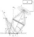
도 3은 시준 동축 조명 시스템(100)인 조명 시스템(100)의 발명 개념의 일 실시형태를 보인 개략도이다. 본 발명의 조명 시스템(100)은 광각 동축 조명의 기능과 시준 동축 조명의 기능을 하나의 면광원(2)에 결합한다. 구성가능 면광원(2)은 상이한 면적 직경(21, 22, ..., 2N)이 선택 또는 초기화될 수 있도록 구성된다.3 is a schematic diagram illustrating one embodiment of the inventive concept of an
면적 직경(21)과 같은 매우 작은 면적 직경의 경우에, 조명 시스템(100)은 점광원 기능을 이용하는 도 2의 조명 시스템(100)에 필적한다. 최소 면적 직경(21)을 선택하면 매우 좁은 빔의 시준 동축 조명이 얻어진다.For very small areal diameters, such as
전체 면적의 경우에, 구성가능 면광원(2)의 최대 면적 직경(2N)이 선택 또는 초기화되고, 이 구성은 확산 면광원(2)이 도 2의 점광원(15)의 위치에 있는 도 1의 확산 면광원(2)을 구비한 구성에 필적한다. 그 결과 매우 넓은 빔 동축 조명을 가진 시준 동축 조명이 얻어진다. 이 조명은 종래의 "광각 동축 조명"으로부터 오는 광에 필적한다. 본 발명에 따르면, 구성가능 면광원(2)으로부터의 광은 이제 조명 렌즈(12)를 통하여 빔 스플리터(4)에 투사되고, 그로부터 샘플(6)의 표면(5)에 투사된다.In the case of total area, the maximum
면광원(2)은 조명 빔 경로(21)의 광축(20)에 배열된다. 전술한 바와 같이, 구성가능 면광원(2)은 상이한 설정가능 면적 직경(21, 22, ..., 2N)이 상이한 빔 직경을 야기하도록 구성된다. 최소 면적 직경(21)과 최대 면적 직경(2N) 사이의 임의의 면적 직경(21, 22, ..., 2N)은 시준 빔 개방 각(22)을 변화시킨다.The
외측 면적 직경(22, ..., 2N)만이 사용되도록(광을 송출하도록) 구성가능 면광원(2)이 설정된 경우에는 구성가능 면광원(2)의 중심(2C)에 어두운 스팟이 유지된다. 이 구성은 암시야 근접 동축 조명을 야기한다.If the configurable surface
조명 빔 경로(21)의 조명 렌즈(12)는 시준 빔을 물체(6)의 표면(5)상의 시야(13)에 조명한다. 물체(6)의 표면(5)으로부터, 시야(13)는 이미징 빔 경로(81)의 이미징 광축(80)을 따라 이미징 렌즈의 이미징 렌즈 동공(조리개)(83)에 이미징된다(여기에서 이미징 렌즈와 카메라는 도시 생략됨).The
도 4는 조명 시스템(100)의 발명 개념의 다른 실시형태를 보인 개략도이다. 빔 스플리터(4)는 생략되었다. 구성가능 면광원(2)은 조명 빔 경로(21)의 광축(20)이 물체(6)의 표면(5)에 대하여 소정 각도(α)로 기울어지도록 배열된다. 전술한 바와 같이, 면광원(2)으로부터의 광은 조명 렌즈(12)에 의해 물체(6)의 표면(5)상에 이미징된다. 물체(6)의 표면(5)으로부터 반사된 광은 조명 빔 경로(81)의 이미징 광축(80)을 따라 전파한다. 물체(6)의 표면(5)에서의 시야(13)는 이미징 렌즈 동공(조리개)(83)에 이미징된다(이미징 렌즈와 카메라는 도시 생략됨). 이미징 빔 경로(81)의 이미징 광축(80)은 물체(6)의 표면(5)에 대하여 소정 각도(β)로 기울어진다. 조명 시스템(100)의 광학 구성은 조명 빔 경로(21)의 광축(20)의 각도(α)의 값이 이미징 빔 경로(81)의 이미징 광축(80)의 각도(β)의 값과 동일하게 되도록 된다. 빔 스플리터를 사용하지 않고 명시야 조명이 달성된다. 다시 말해서, 조명 각(α)의 값이 이미징 각(β)의 값과 동일한 검사 도구가 얻어진다.4 is a schematic diagram illustrating another embodiment of the inventive concept of the
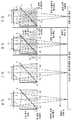
도 5는 조명 렌즈(12)를 사용하지 않는 경우에 시준 빔 개방 각(84)의 값 정도를 보인 개략도이다. 조명 렌즈(12) 대신에, 면광원(여기에서는 도시 생략됨)의 확산판(11)이 빔 스플리터(4) 앞에 배치된다. 넓은 빔이고 조명 렌즈(12)가 없는 경우에 물체(6)의 조명으로부터의 결과로서, 전통적인 넓은 동축 조명인 비대칭의 넓은 빔이 얻어진다. 넓은 빔 개방 각(22)(도 3 참조) 때문에, 카메라(8)에서 물체(6)의 이미징 품질은 물체의 표면(5)의 기울기에 민감하지 않을 것이다.5 is a schematic diagram showing the degree of value of the collimating
도 6 내지 도 8은 조명 광의 스팟 크기(면적 직경)로부터 시준 빔 개방 각(84)의 의존성을 보인 도이다. 도 6은 큰 스팟 크기(큰 면적 직경) 및 조명 렌즈(12)를 가진 구성가능 면광원(2)을 이용하는 시준 빔 개방 각(84)의 정도를 보인 개략도이다. 구성가능 면광원에 의해 설정된 큰 스팟 크기(큰 면적 직경)에 기인하여, 시준 빔 개방 각(84)의 일부(24)는 컷오프된다. 이 때문에 빔 개방 각(84)은 시야(13)의 가장자리 쪽으로 비대칭으로 된다. 물체(6)의 표면(5)으로부터 반사된 광은 빔 스플리터(4)의 기울기에 민감하지 않다. 도 7은 중간 스팟 크기(도 6에 비하여 감소된 스팟 크기)를 가진 구성가능 면광원을 이용하는 시준 빔 개방 각(84)의 정도를 보인 개략도이다. 조명 렌즈(12)로부터, 구성가능 면광원으로부터의 광은 빔 스플리터(4)를 통해 물체(6)의 표면에 시준된다. 도 7로부터, 스팟 크기가 감소되면 시준 빔 개방 각(84)이 더 좁아진다는 것을 알 수 있다. 추가로, 물체(6)의 표면(5)으로부터 반사된 광은 이제 물체(6)의 표면(5)의 기울기에 민감하다. 도 8은 시준 빔 개방 각(84)의 정도를 보인 개략도이다. 도 7의 개략도와 비교할 때 스팟 크기가 더욱 감소된다. 구성가능 면광원(2)은 이제 작은 스팟 크기(작은 면적 직경)을 갖는다. 좁은 빔 개방 각의 결과로서 조명 시스템의 구성은 물체(6)의 표면(5)의 기울기에 매우 민감하다. 추가로, 물체(6)의 표면(5)으로부터 반사된 광은 도 6 또는 도 7에 도시된 스팟 크기(면적 직경)에 비하여 더 시준된다.6 to 8 are diagrams showing the dependence of the collimated
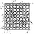
도 9는 구성가능 면광원(2)의 일 실시형태의 상면도이다. 여기에 도시된 실시형태에 있어서, 면광원(2)은 캐리어(16)에 2차원 방식으로 배열된 복수의 발광 요소(14)에 의해 구성된다. 여기에서 발광 요소(14)는 행(171, 172, ..., 17N)과 열(181, 182, ..., 18N)로 배열되고, 이로써 매트릭스를 형성한다. 가능한 일 실시형태에 따르면, 발광 요소(14)는 발광 다이오드(LED)이다. 도 3 및 도 4에 도시된 바와 같이, 구성가능 면광원(2)은 제어 및 구동 장치(30)에, 또는 그에 따라서 면광원(2)을 어드레싱할 수 있는 임의의 매립형 시스템에 할당된다. 제어 및 구동 장치(30)에 의해, 개별 발광 요소(14)를 어드레싱하고 구성가능 면광원(2)의 상이한 발광 형상 및/또는 크기를 발생하는 것이 가능해진다. 도 9는 구성가능 면광원(2)의 상이한 크기(191, 192, ..., 19N)가 어떻게 초기화되는지에 대한 일 실시형태를 보인 것이다. 발광 요소(14)는 면광원(2)의 원의 각종 크기가 어드레싱되도록 제어 및 구동 장치(30)에 의해 어드레싱된다. 구성가능 면광원(2)의 원의 어드레싱 가능한 형태는 제한하는 인수로서 생각되지 않는다는 점에 주목하여야 한다.9 is a top view of an embodiment of a configurable surface
도 10은 도 9의 구성가능 면광원(2)의 실시형태의 측면도이다. 발광 요소(14)는 캐리어(16) 위에 배열된다. 구성가능 면광원(2)은 캐리어(16) 위에서 어드레싱된 발광 요소(14)의 균일한 광 분포(면적)를 달성하기 위해 확산기(diffuser)(도시 생략됨)가 추가로 제공될 수 있다.FIG. 10 is a side view of an embodiment of the configurable surface
구성가능 면광원(2)은 전형적으로 동심 기하학적 형상(23)으로 이루어진 영역을 가질 수 있다. 이상적인 해법은 동심 원형(25)을 사용하는 것이다. 이 실시형태는 도 11에 도시되어 있고, 여기에서 구성가능 면광원(2)은 동심 원형(25)의 형상으로 이미 배치된 발광 요소(14)에 의해 형성된다.The configurable surface
도 12는 구성가능 면광원(2)의 다른 실시형태를 보인 것이다. 발광 요소(14)의 배치를 위한 가장 용이한 해법은 동심 직사각형(26)을 사용하는 것이다. 기하학적 형상(23)은 직사각형이고, 이것은 평행 각이 직사각형의 수평/수직 방향에 대하여 대각선 방향에서 다르다는 단점을 갖는다.12 shows another embodiment of a configurable surface
도 13은 구성가능 면광원(2)의 또 다른 실시형태를 보인 것이다. 도 12에 도시된 실시형태에 비하여 양호한 절충안은 동심 형상(23)으로서 동심 육각형(27)을 사용하는 것이다. 이것은 예를 들면 발광 요소(14)의 엇갈림 격자를 만들어서 달성할 수 있다(여기에서는 도시 생략됨).13 shows another embodiment of a configurable surface
그러나 면광원의 설계는 도 11 내지 도 13에 도시된 동심 기하학적 형상(23)으로 제한되지 않는다. 사실 면광원(2)의 발광 요소(14)를 다룸으로써 임의의 패턴이 투사될 수 있다. 이것은 광빔이 원하는 패턴 및 원하는 광빔 개방 각을 갖게 할 것이다.However, the design of the surface light source is not limited to the
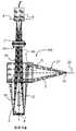
도 14는 본 발명의 조명 시스템(100)을 검사 장치(200)에 통합하는 가능한 실시형태를 보인 것이다. 본 발명의 조명 시스템(100)은 검사 장치(200)의 기존 하우징(40) 내에 통합된다. 본 발명의 조명 시스템(100)은 하나의 동축 조명 구성에서 상이한 광빔 개방 각을 제공한다. 구성가능 면광원(2)으로부터의 광(10)은 미러(41)를 통해 조명 렌즈(12)(조명 렌즈(12)의 가능한 일 실시형태는 프레넬 렌즈이다)에 지향된다. 미러(41)는 조명 빔 경로(21)를 꺾기 위해 필요하다. 이것은 공간을 절약하고 검사 장치(200)에 대한 조명 시스템(100)의 통합을 가능하게 한다.14 shows a possible embodiment of integrating the
본 발명 조명 시스템(100)의 빔 스플리터(4)는 홀더(43)에 장착된다. 검사 대상의 물체(6)는 물체(6)의 표면(5)이 홀더(43)의 제1 측면(43A)에 대면하도록 캐리어(45)에 의해 유지된다. 미러(41)는 구성가능 면광원(2)으로부터의 조명 광(10)이 조명 렌즈(12)를 통해 빔 스플리터(4)에 지향되고 그로부터 물체(6)의 표면(5)에 지향되도록 상기 홀더(43)의 제2 측면(43B)에 장착된다.The
물체(6)의 표면(5)으로부터 반사된 광은 이미징 빔 경로(81)를 따라 카메라(8)로 진행한다. 이미징 렌즈(7)는 물체(6)의 표면(5)의 시야(13)를 카메라(8)의 이미지 평면(9)에 이미징한다. 여기에 도시된 실시형태에서는 공간적인 이유로 이미징 빔 경로(81)를 꺾기 위해 이미징 빔 경로(81)에 2개의 추가적인 미러(82)가 제공된다. 본 발명의 검사 장치(200)에 의해 하나의 동축 조명 구성에서 상이한 광빔 개방 각을 제공할 수 있다.The light reflected from the
도 15는 구성가능 면광원(2)의 추가적인 실시형태를 보인 것이다. LCD-스크린(50)은 적어도 하나의 발광 요소(14) 이후에 배치된다. 여기에 도시된 실시형태에서는 LCD(50)의 배면의 균일한 면적 조명을 제공하는 단일 발광 요소(14)가 사용된다(도 16에 도시된 구성가능 면광원(2)의 측면도 참조). LCD(50)의 복수의 픽셀(51)들은 개별적으로 어드레싱될 수 있다. LCD(50)는 2차원 방식으로 배열된 복수의 픽셀(51)을 포함한다. 따라서, 공지의 제어 장치(도시 생략됨)에 의해 픽셀(51)들을 개별적으로 다룸으로써 각종 조명 패턴이 형성될 수 있다. 구성가능 면광원(2)의 픽셀(51)(도 15 참조)들은 한 그룹의 픽셀들이 발광 요소(14)로부터의 광(55)을 완전히 차단하고 다른 픽셀(51)들은 발광 요소(14)로부터의 광(55)이 통과(도 16 참조)되게 하는 방식으로 어드레싱된다. 당업자라면 개별 픽셀(51)들의 투과율이 또한 조정될 수 있다는 것을 이해할 것이다.
도 17은 본 발명의 조명 시스템(100)을 검사 장치(200)에 통합하는 것의 또 다른 가능한 실시형태를 보인다. 본 발명의 조명 시스템(100)은 검사 장치(200)의 기존 하우징(40) 내에 통합된다. 본 발명의 조명 시스템(100)은 하나의 동축 조명 구성에서 상이한 광빔 개방 각을 제공한다. 구성가능 면광원(2)으로부터의 광(10)은 조명 렌즈(12)(조명 렌즈(12)의 가능한 일 실시형태는 프레넬 렌즈이다)에 지향된다. 본 발명의 조명 시스템(100)의 빔 스플리터(4)는 홀더(43) 내에 장착된다. 검사 대상의 물체(6)는 물체(6)의 표면(5)이 홀더(43)의 제1 측면(43A)에 대면하도록 캐리어(45)에 의해 유지된다. 구성가능 면광원(2)은 조명 광(10)이 조명 렌즈(12)를 통해 빔 스플리터(4)에 지향되고 그로부터 물체(6)의 표면(5)에 지향되도록 상기 홀더(43)의 제2 측면(43B)에 장착된다. 물체(6)의 표면(5)으로부터 반사된 광은 이미징 빔 경로(81)를 따라 카메라(8)로 진행한다. 이미징 렌즈(7)는 물체(6)의 표면(5)의 시야(13)를 카메라(8)의 이미지 평면(9)에 이미징한다. 여기에 도시된 실시형태에서는 공간적인 이유로 이미징 빔 경로(81)를 꺾기 위해 이미징 빔 경로(81)에 2개의 추가적인 미러(82)가 제공된다. 본 발명의 검사 장치(200)에 의해 하나의 동축 조명 구성에서 상이한 광빔 개방 각을 제공할 수 있다.15 shows a further embodiment of a configurable surface
17 shows another possible embodiment of the integration of the
상기 설명에서, 본 발명 실시형태의 완전한 이해를 제공하기 위해 다수의 특정 세부들이 개시되었다. 그러나 예시된 본 발명 실시형태의 전술한 설명은 총 망라적이거나 본 발명을 개시된 정확한 형태로 제한하는 것으로 의도되지 않는다. 당업자라면 본 발명이 하나 이상의 특정 세부 없이, 또는 다른 방법, 컴포넌트 등에 의해 실시될 수 있다는 것을 이해할 것이다. 다른 예로서, 잘 알려진 구조 또는 동작은 발명의 양태를 불명료하게 하는 것을 피하기 위해 구체적으로 도시 또는 설명하지 않았다. 발명의 특정 실시형태 및 그 예를 예시 목적으로 여기에서 설명하였지만, 당업자라면 이해하는 바와 같이 발명의 범위 내에서 각종의 등가적인 수정이 가능하다.In the foregoing description, numerous specific details have been set forth in order to provide a thorough understanding of embodiments of the present invention. However, the foregoing description of illustrated embodiments of the invention is not intended to be exhaustive or to limit the invention to the precise form disclosed. It will be understood by those skilled in the art that the present invention may be practiced without one or more of the specific details, or by other methods, components, or the like. In other instances, well-known structures or acts have not been specifically shown or described in order to avoid obscuring aspects of the invention. Although specific embodiments of the invention and examples thereof have been described herein for purposes of illustration, various equivalent modifications are possible within the scope of the invention as those skilled in the art will understand.
이러한 수정은 전술한 상세한 설명에 비추어 본 발명에 대하여 행하여질 수 있다. 이하의 특허 청구범위에서 사용하는 용어들은 발명을 전술한 상세한 설명 및 특허 청구범위에서 개시된 특정 실시형태로 제한하는 것으로 추론되지 않아야 한다. 오히려, 발명의 범위는 이하의 특허 청구범위에 의해 결정되어야 하고, 특허 청구범위는 특허 청구범위 해석에 관한 확립된 원칙에 따라 추론되어야 한다.Such modifications may be made to the present invention in light of the foregoing detailed description. The terms used in the following claims should not be construed as limiting the invention to the specific embodiments disclosed in the foregoing detailed description and claims. Rather, the scope of the invention should be determined by the following claims, which should be construed in accordance with established principles for interpretation of claims.
2면광원; 구성가능 면광원
21, 22, ..., 2N면적 직경
2C면광원의 중심
3광
4빔 스플리터
5표면
6물체
7이미징 렌즈
8카메라
9이미지 평면
10광
11확산판
12조명 렌즈
13시야
14발광 요소
15점광원
16캐리어
171, 172, ..., 17N행
181, 182, ..., 18N열
191, 192, ..., 19N크기
20조명 광축
21조명 빔 경로
22시준 빔 개방 각(조명 렌즈 이전)
23동심 기하학적 형상
24부분
25동심 원형
26동심 직사각형
27동심 육각형
30제어 및 구동 장치
40하우징
41미러
43홀더
43A제1 측면
43B제2 측면
50LCD
51LCD의 픽셀
55광
80이미징 광축
81이미징 빔 경로
82미러
83이미징 렌즈 동공, 조리개
84시준 빔 개방 각(이미징 렌즈 이후)
100조명 시스템
200검사 장치
D방향
α각
β각two-sided light source; Configurable surface light source
21 , 22 , ..., 2N area diameter
Center of 2C surface light source
3 light
4 beam splitter
5 surface
6 objects
7 imaging lens
8 camera
9 image plane
10 light
11 diffuser
12 light lenses
13 sight
14 luminous element
15 point light source
16 carrier
171 , 172 , ..., 17N rows
181 , 182 , ..., 18N columns
191 , 192 , ..., 19N size
20 light axis
21 light beam path
22 collimating beam opening angle (before illumination lens)
23 Concentric Geometric Shapes
24 parts
25 concentric circles
26 concentric rectangles
27 concentric hexagons
30 Controls and Drives
40 housing
41 mirror
43 holder
43A first aspect
43B second aspect
50 LCD
51 LCD pixels
55 light
80 imaging optical axis
81 Imaging beam path
82 mirror
83 imaging lens pupil, aperture
84 collimating beam opening angle (after imaging lens)
100 lighting systems
200 inspection device
D direction
α angle
β angle
Claims (42)
Translated fromKorean조명 빔 경로의 조명 광축에 배열된 구성가능 면광원(configurable area light source) - 상기 구성가능 면광원은 제1 형상과 제2 형상 사이에서 실시간으로 상이한 빔 형상이 설정가능하도록 구성되며, 상기 제1 형상은 상기 제2 형상과 상이함 - ;
이미징 빔 경로의 이미징 광축;
물체의 표면상의 시야에 시준 빔을 지향시키기(directing) 위해 상기 조명 빔 경로에 배치된 적어도 하나의 조명 렌즈 - 상기 조명 빔 경로의 조명 광축의 입사각의 값은 상기 이미징 빔 경로의 이미징 광축의 반사각의 값과 동일함 - ;
상기 적어도 하나의 조명 렌즈 이후의 조명 빔 경로에 배치된 빔 스플리터;
미러;
홀더 - 상기 빔 스플리터는 상기 홀더 내에 장착되고, 상기 미러는 상기 구성가능 면광원으로부터 방출된 광이 상기 미러로부터 상기 적어도 하나의 조명 렌즈로 지향되도록 상기 홀더에 장착됨 - ; 및
상이한 빔 직경을 얻기 위해 조명에 대한 복수의 동심 기하학적 형상이 발생되도록 상기 구성가능 면광원에 할당된 제어 및 구동 장치
를 포함하는, 시준 조명용 조명 시스템.An illumination system for collimated illumination, comprising:
a configurable area light source arranged in an illumination optical axis of an illumination beam path, the configurable area light source being configured to be configurable of a different beam shape in real time between a first shape and a second shape, the first shape being configurable shape is different from said second shape;
the imaging optical axis of the imaging beam path;
at least one illumination lens disposed in the illumination beam path for directing a collimating beam into a field of view on the surface of the object, the value of the angle of incidence of the illumination optical axis of the illumination beam path being the angle of reflection of the imaging optical axis of the imaging beam path Same as value - ;
a beam splitter disposed in an illumination beam path after the at least one illumination lens;
mirror;
a holder, the beam splitter mounted within the holder, the mirror mounted to the holder such that light emitted from the configurable surface light source is directed from the mirror to the at least one illumination lens; and
A control and drive device assigned to the configurable surface light source to generate a plurality of concentric geometries for illumination to achieve different beam diameters.
A lighting system for collimated lighting comprising a.
균일한 면적 조명(homogeneous area illumination)을 제공하는 단일 발광 요소; 및
상기 단일 발광 요소 앞에 배치된 LCD-스크린
을 포함한 것인, 시준 조명용 조명 시스템.The method of claim 1 , wherein the configurable surface light source comprises:
a single light emitting element that provides homogeneous area illumination; and
LCD-screen disposed in front of the single light emitting element
A lighting system for collimated lighting, including a.
조명 빔 경로의 조명 광축에 배열된 구성가능 면광원(configurable area light source) - 상기 구성가능 면광원은 제1 형상과 제2 형상 사이에서 실시간으로 상이한 빔 형상이 설정가능하도록 구성되며, 상기 제1 형상은 상기 제2 형상과 상이함 - ;
이미징 빔 경로의 이미징 광축;
물체의 표면상의 시야에 시준 빔을 지향시키기(directing) 위해 상기 조명 빔 경로에 배치된 적어도 하나의 조명 렌즈 - 상기 조명 빔 경로의 조명 광축의 입사각의 값은 상기 이미징 빔 경로의 이미징 광축의 반사각의 값과 동일함 - ;
상기 적어도 하나의 조명 렌즈 이후의 조명 빔 경로에 배치된 빔 스플리터;
미러; 및
홀더 - 상기 빔 스플리터는 상기 홀더 내에 장착되고, 상기 미러는 상기 구성가능 면광원으로부터 방출된 광이 상기 미러로부터 상기 적어도 하나의 조명 렌즈로 지향되도록 상기 홀더에 장착됨 -
를 포함하고,
상기 구성가능 면광원은 복수의 발광 요소의 2차원 배열이며,
상기 복수의 발광 요소는 복수의 발광 다이오드를 포함하고,
상기 복수의 발광 요소의 2차원 배열은 복수의 동심 기하학적 형상의 상기 복수의 발광 요소의 배열에 의해 규정되는 것인, 시준 조명용 조명 시스템.An illumination system for collimated illumination, comprising:
a configurable area light source arranged in an illumination optical axis of an illumination beam path, the configurable area light source being configured to be configurable of a different beam shape in real time between a first shape and a second shape, the first shape being configurable shape is different from said second shape;
the imaging optical axis of the imaging beam path;
at least one illumination lens disposed in the illumination beam path for directing a collimating beam into a field of view on the surface of the object, the value of the angle of incidence of the illumination optical axis of the illumination beam path being the angle of reflection of the imaging optical axis of the imaging beam path Same as value - ;
a beam splitter disposed in an illumination beam path after the at least one illumination lens;
mirror; and
a holder, wherein the beam splitter is mounted within the holder, the mirror mounted to the holder such that light emitted from the configurable surface light source is directed from the mirror to the at least one illumination lens;
including,
wherein the configurable surface light source is a two-dimensional arrangement of a plurality of light emitting elements;
wherein the plurality of light emitting elements comprises a plurality of light emitting diodes;
wherein the two-dimensional arrangement of the plurality of light-emitting elements is defined by an arrangement of the plurality of light-emitting elements of a plurality of concentric geometric shapes.
상이한 빔 직경을 얻기 위해 개별적인 동심 기하학적 형상의 상기 복수의 발광 요소를 구동하도록 상기 복수의 발광 요소의 상기 복수의 동심 기하학적 형상의 배열에 할당된 제어 및 구동 장치
를 더 포함하는, 시준 조명용 조명 시스템.15. The method of claim 14,
a control and drive device assigned to the arrangement of the plurality of concentric geometries of the plurality of light emitting elements to drive the plurality of light emitting elements of respective concentric geometries to obtain different beam diameters
A lighting system for collimated lighting further comprising a.
이미징 빔 경로의 이미징 광축에 배열된 카메라;
물체의 표면의 적어도 일부를 상기 카메라의 이미지 평면에 이미징하기 위해 상기 이미징 빔 경로에 배치된 이미징 렌즈;
구성가능 면광원을 구비한 조명 시스템 - 상기 구성가능 면광원은 조명 빔 경로의 조명 광축에 배열되고, 상기 구성가능 면광원은 상이한 빔 형상이 제1 형상과 제2 형상 사이에서 실시간으로 설정가능하도록 구성되며, 상기 제1 형상은 상기 제2 형상과 상이함 - ;
물체의 표면상의 시야에 시준 빔을 지향시키기 위해 상기 조명 빔 경로에 배치된 적어도 하나의 조명 렌즈 - 상기 조명 빔 경로의 상기 조명 광축의 입사각의 값은 상기 이미징 빔 경로의 이미징 광축의 반사각의 값과 동일함 - ;
상기 적어도 하나의 조명 렌즈 이후의 조명 빔 경로에 배치된 빔 스플리터;
미러; 및
홀더 - 상기 빔 스플리터는 상기 홀더 내에 장착되고, 상기 미러는 상기 구성가능 면광원으로부터 방출된 광이 상기 미러로부터 상기 적어도 하나의 조명 렌즈로 지향되도록 상기 홀더에 장착됨 - ; 및
상이한 빔 직경을 얻기 위해 조명의 복수의 동심 기하학적 형상이 발생되도록 상기 구성가능 면광원에 할당된 제어 및 구동 장치
를 포함하는, 검사 도구.In the inspection tool,
a camera arranged in the imaging optical axis of the imaging beam path;
an imaging lens disposed in the imaging beam path for imaging at least a portion of the surface of the object in the image plane of the camera;
Illumination system having a configurable surface light source, wherein the configurable surface light source is arranged in an illumination optical axis of an illumination beam path, the configurable surface light source such that different beam shapes are settable between a first shape and a second shape in real time wherein the first shape is different from the second shape;
at least one illumination lens disposed in the illumination beam path for directing a collimating beam into a field of view on the surface of the object, wherein the value of the angle of incidence of the illumination optical axis of the illumination beam path is equal to the value of the reflection angle of the imaging optical axis of the imaging beam path Same - ;
a beam splitter disposed in an illumination beam path after the at least one illumination lens;
mirror; and
a holder, the beam splitter mounted within the holder, the mirror mounted to the holder such that light emitted from the configurable surface light source is directed from the mirror to the at least one illumination lens; and
A control and drive device assigned to the configurable surface light source to generate a plurality of concentric geometries of illumination to achieve different beam diameters.
Including, inspection tool.
상기 빔 스플리터는 상기 조명 빔 경로의 재지향된 광축을 따라 상기 구성가능 면광원으로부터의 시준 조명 광을 상기 물체의 표면에 지향시키며, 상기 이미징 빔 경로의 이미징 광축은 상기 조명 빔 경로의 재지향된 광축과 동축인 것인, 검사 도구.21. The method of claim 20,
The beam splitter directs collimated illumination light from the configurable surface light source to a surface of the object along a redirected optical axis of the illumination beam path, the imaging optical axis of the imaging beam path being the redirected optical axis of the illumination beam path and A coaxial one, an inspection tool.
샘플 캐리어
를 더 포함하고,
상기 물체의 표면은 상기 샘플 캐리어에 의해 유지되고 상기 홀더의 제1 측면에 대면하며,
상기 미러는 상기 구성가능 면광원으로부터의 광이 상기 적어도 하나의 조명 렌즈로 지향되도록 상기 홀더의 제2 측면에 장착되는 것인, 검사 도구.22. The method of claim 21,
sample carrier
further comprising,
the surface of the object is held by the sample carrier and faces a first side of the holder;
and the mirror is mounted to the second side of the holder such that light from the configurable surface light source is directed to the at least one illumination lens.
샘플 캐리어
를 더 포함하고,
상기 물체의 표면은 상기 샘플 캐리어에 의해 유지되고 상기 홀더의 제1 측면에 대면하며,
상기 홀더의 제2 측면은 상기 구성가능 면광원으로부터의 광이 상기 빔 스플리터에 부딪히도록 상기 구성가능 면광원을 반송(carry)하는 것인, 검사 도구.22. The method of claim 21,
sample carrier
further comprising,
the surface of the object is held by the sample carrier and faces a first side of the holder;
and the second side of the holder carries the configurable surface light source such that light from the configurable surface light source strikes the beam splitter.
2차원 배열로 캐리어상에 배치되고, 상기 구성가능 면광원을 규정하는 복수의 발광 요소 - 상기 복수의 발광 요소는 상기 복수의 발광 요소 중의 발광 요소가 개별적으로 어드레싱 가능하고 복수의 패턴이 상기 구성가능 면광원에 의해 달성될 수 있도록 상기 제어 및 구동 장치에 할당됨 - ; 및
광빔 개방 각을 갖는 복수의 패턴 내의 패턴에 따라 발생된 광빔
을 더 포함하는, 검사 도구.21. The method of claim 20,
a plurality of light emitting elements disposed on a carrier in a two-dimensional arrangement, the plurality of light emitting elements defining said configurable surface light source, said plurality of light emitting elements being individually addressable of said plurality of light emitting elements and said plurality of patterns being said configurable assigned to said control and drive device to be achieved by means of a surface light source; and
A light beam generated according to a pattern in a plurality of patterns having a light beam opening angle
Further comprising, an inspection tool.
균일한 면적 조명을 제공하는 단일 발광 요소, 및
상기 단일 발광 요소 앞에 배치된 LCD-스크린을 포함하는 것인, 검사 도구.21. The method of claim 20, wherein the configurable surface light source comprises:
a single light emitting element that provides uniform area illumination, and
and an LCD-screen disposed in front of the single light emitting element.
상기 LCD-스크린은 2차원 배열의 복수의 개별 픽셀을 포함하고, 상기 개별 픽셀은 개별 픽셀의 투과율 값을 변경하기 위해 상기 제어 및 구동 장치에 의해 어드레싱 가능한 것인, 검사 도구.28. The method of claim 27,
wherein the LCD-screen comprises a plurality of individual pixels in a two-dimensional arrangement, the individual pixels being addressable by the control and drive device to change the transmittance value of the individual pixels.
이미징 빔 경로의 이미징 광축에 배열된 카메라;
물체의 표면의 적어도 일부를 상기 카메라의 이미지 평면에 이미징하기 위해 상기 이미징 빔 경로에 배치된 이미징 렌즈;
구성가능 면광원을 구비한 조명 시스템 - 상기 구성가능 면광원은 조명 빔 경로의 조명 광축에 배열되고, 상기 구성가능 면광원은 상이한 빔 형상이 제1 형상과 제2 형상 사이에서 실시간으로 설정가능하도록 구성되며, 상기 제1 형상은 상기 제2 형상과 상이함 - ;
물체의 표면상의 시야에 시준 빔을 지향시키기 위해 상기 조명 빔 경로에 배치된 적어도 하나의 조명 렌즈 - 상기 조명 빔 경로의 상기 조명 광축의 입사각의 값은 상기 이미징 빔 경로의 이미징 광축의 반사각의 값과 동일함 - ;
상기 적어도 하나의 조명 렌즈 이후의 조명 빔 경로에 배치된 빔 스플리터;
미러; 및
홀더 - 상기 빔 스플리터는 상기 홀더 내에 장착되고, 상기 미러는 상기 구성가능 면광원으로부터 방출된 광이 상기 미러로부터 상기 적어도 하나의 조명 렌즈로 지향되도록 상기 홀더에 장착됨 -
를 포함하고,
상기 조명 빔 경로는 상기 구성가능 면광원으로부터의 광을 상기 물체의 표면에 지향시키기 위해 적어도 1회 꺾어지는 것인, 검사 도구.In the inspection tool,
a camera arranged in the imaging optical axis of the imaging beam path;
an imaging lens disposed in the imaging beam path for imaging at least a portion of the surface of the object in the image plane of the camera;
Illumination system having a configurable surface light source, wherein the configurable surface light source is arranged in an illumination optical axis of an illumination beam path, the configurable surface light source such that different beam shapes are settable between a first shape and a second shape in real time wherein the first shape is different from the second shape;
at least one illumination lens disposed in the illumination beam path for directing a collimating beam into a field of view on the surface of the object, wherein the value of the angle of incidence of the illumination optical axis of the illumination beam path is equal to the value of the reflection angle of the imaging optical axis of the imaging beam path Same - ;
a beam splitter disposed in an illumination beam path after the at least one illumination lens;
mirror; and
a holder, wherein the beam splitter is mounted within the holder, the mirror mounted to the holder such that light emitted from the configurable surface light source is directed from the mirror to the at least one illumination lens;
including,
and the illumination beam path is bent at least once to direct light from the configurable surface light source to a surface of the object.
(a) 광빔 개방 각을 규정하는 조명 광을, 조명 빔 경로를 따라 구성가능 면광원으로부터, 홀더에 장착된 미러를 통해 조명 렌즈로, 상기 홀더 내에 장착된 빔 스플리터를 관통하여, 물체의 표면에 지향시키는 단계;
(b) 상기 물체의 표면으로부터의 반사광을 이미징 빔 경로를 따라 지향시키는 단계;
(c) 상기 물체의 표면으로부터의 반사광을 이미징 렌즈에 의해 카메라의 이미지 평면에 이미징하는 단계;
(d) 제1 형상으로부터 제2 형상으로 상기 조명 광의 형상을 변경하는 단계 - 상기 제1 형상은 제2 형상과는 상이함 - ;
(e) 상기 단계 (a) 내지 (d)를 반복하는 단계; 및
(f) 각각 상기 제1 형상 및 상기 제2 형상을 갖는 실시간 이미지로 상기 물체 표면상에 시야를 발생시키는 단계
를 포함하고,
상기 물체 검사 방법은, 상이한 빔 직경을 얻기 위해 복수의 동심 및 어드레싱 가능한(addressable) 기하학적 형상이 발생되도록 상기 구성가능 면광원에 제어 및 구동 장치를 할당하는 단계를 더 포함하는, 물체 검사 방법.In the object inspection method,
(a) directing illumination light defining a light beam opening angle from a configurable surface light source along an illumination beam path to an illumination lens through a mirror mounted in the holder and through a beam splitter mounted in the holder to the surface of an object directing;
(b) directing reflected light from the surface of the object along an imaging beam path;
(c) imaging the reflected light from the surface of the object by an imaging lens into the image plane of the camera;
(d) changing a shape of the illumination light from a first shape to a second shape, wherein the first shape is different from the second shape;
(e) repeating steps (a) to (d); and
(f) generating a field of view on the object surface with real-time images each having the first shape and the second shape, respectively.
including,
The method of inspecting an object further comprising assigning a control and drive device to the configurable surface light source such that a plurality of concentric and addressable geometries are generated to obtain different beam diameters.
규정된 광 직경이 달성되도록 상기 구성가능 면광원을 제어 및 구동함으로써 발생되는 상이한 광 직경에 의해 상기 광빔의 상이한 개방 각을 설정하는 단계
를 더 포함하는, 물체 검사 방법.34. The method of claim 33,
setting different opening angles of the light beams by different light diameters generated by controlling and driving the configurable surface light source such that a prescribed light diameter is achieved.
Further comprising, an object inspection method.
(a) 광빔 개방 각을 규정하는 조명 광을, 조명 빔 경로를 따라 구성가능 면광원으로부터, 홀더에 장착된 미러를 통해 조명 렌즈로, 상기 홀더 내에 장착된 빔 스플리터를 관통하여, 물체의 표면에 지향시키는 단계;
(b) 상기 물체의 표면으로부터의 반사광을 이미징 빔 경로를 따라 지향시키는 단계;
(c) 상기 물체의 표면으로부터의 반사광을 이미징 렌즈에 의해 카메라의 이미지 평면에 이미징하는 단계;
(d) 제1 형상으로부터 제2 형상으로 상기 조명 광의 형상을 변경하는 단계 - 상기 제1 형상은 제2 형상과는 상이함 - ;
(e) 상기 단계 (a) 내지 (d)를 반복하는 단계; 및
(f) 각각 상기 제1 형상 및 상기 제2 형상을 갖는 실시간 이미지로 상기 물체 표면상에 시야를 발생시키는 단계
를 포함하고,
상기 구성가능 면광원은 복수의 발광 요소의 매트릭스 배열이며,
상기 물체 검사 방법은,
상기 복수의 발광 요소를 동심 기하학적 형상으로 배열하는 단계; 및
제어 및 구동 장치에 의해, 상이한 빔 직경을 얻기 위해 상기 동심 기하학적 형상을 어드레싱 단계
를 더 포함하는, 물체 검사 방법.In the object inspection method,
(a) directing illumination light defining a light beam opening angle from a configurable surface light source along an illumination beam path to an illumination lens through a mirror mounted in the holder and through a beam splitter mounted in the holder to the surface of an object directing;
(b) directing reflected light from the surface of the object along an imaging beam path;
(c) imaging the reflected light from the surface of the object by an imaging lens into the image plane of the camera;
(d) changing a shape of the illumination light from a first shape to a second shape, wherein the first shape is different from the second shape;
(e) repeating steps (a) to (d); and
(f) generating a field of view on the object surface with real-time images each having the first shape and the second shape, respectively.
including,
wherein the configurable surface light source is a matrix arrangement of a plurality of light emitting elements;
The object inspection method includes:
arranging the plurality of light emitting elements in concentric geometric shapes; and
addressing said concentric geometry to obtain different beam diameters by means of a control and drive device;
Further comprising, an object inspection method.
조명 빔 경로의 조명 광축에 배열된 구성가능 면광원 - 상기 구성가능 면광원은 제1 형상과 제2 형상 사이에서 실시간으로 상이한 빔 형상이 설정가능하도록 구성되며, 상기 제1 형상은 상기 제2 형상과 상이함 - ;
적어도 하나의 조명 렌즈 이후의 조명 빔 경로에 배치되는 빔 스플리터 - 상기 빔 스플리터는 상기 조명 빔 경로의 재지향된 조명 광축을 따라 상기 구성가능 면광원으로부터의 시준 조명 광을 물체의 표면에 지향시키고, 이미징 빔 경로의 이미징 광축은 상기 조명 빔 경로의 재지향된 광축과 동축임 - ;
물체의 표면상의 시야에 시준 빔을 지향시키기 위해 상기 조명 빔 경로에 배치된 적어도 하나의 조명 렌즈 - 상기 조명 빔 경로의 광축의 입사각의 값은 상기 이미징 빔 경로의 광축의 반사각의 값과 동일함 - ;
미러;
홀더 - 상기 빔 스플리터가 상기 홀더 내에 장착되고, 상기 미러는 상기 구성가능 면광원으로부터 방출된 광이 상기 미러로부터 상기 적어도 하나의 조명 렌즈로 지향되도록 상기 홀더에 장착됨 - ; 및
상이한 빔 직경을 얻기 위해 복수의 동심 기하학적 형상이 상기 구성가능 면광원에 의해 발생되도록 상기 구성가능 면광원에 할당된 제어 및 구동 장치
를 포함하는, 시준 조명용 조명 시스템.A lighting system for collimated lighting, comprising:
a configurable surface light source arranged in an illumination optical axis of an illumination beam path, wherein the configurable surface light source is configured such that a different beam shape is settable between a first shape and a second shape in real time, the first shape being the second shape different from - ;
a beam splitter disposed in the illumination beam path after the at least one illumination lens, the beam splitter directing collimated illumination light from the configurable surface light source along a redirected illumination optical axis of the illumination beam path to a surface of the object; the imaging optical axis of the beam path is coaxial with the redirected optical axis of the illumination beam path;
at least one illumination lens disposed in said illumination beam path for directing a collimating beam into a field of view on a surface of an object, wherein a value of an angle of incidence of an optical axis of said illumination beam path is equal to a value of a reflection angle of said optical axis of said imaging beam path; ;
mirror;
a holder, wherein the beam splitter is mounted within the holder, the mirror mounted to the holder such that light emitted from the configurable surface light source is directed from the mirror to the at least one illumination lens; and
A control and drive device assigned to the configurable surface light source such that a plurality of concentric geometries are generated by the configurable surface light source to obtain different beam diameters.
A lighting system for collimated lighting comprising a.
Applications Claiming Priority (3)
| Application Number | Priority Date | Filing Date | Title |
|---|---|---|---|
| US201462073393P | 2014-10-31 | 2014-10-31 | |
| US62/073,393 | 2014-10-31 | ||
| PCT/US2015/058486WO2016070133A1 (en) | 2014-10-31 | 2015-10-30 | Illumination system, inspection tool with illumination system, and method of operating an illumination system |
Publications (2)
| Publication Number | Publication Date |
|---|---|
| KR20170080631A KR20170080631A (en) | 2017-07-10 |
| KR102272438B1true KR102272438B1 (en) | 2021-07-02 |
Family
ID=55858432
Family Applications (1)
| Application Number | Title | Priority Date | Filing Date |
|---|---|---|---|
| KR1020177014639AActiveKR102272438B1 (en) | 2014-10-31 | 2015-10-30 | Illumination system, inspection tool with illumination system, and method of operating an illumination system |
Country Status (9)
| Country | Link |
|---|---|
| EP (1) | EP3140638B1 (en) |
| JP (2) | JP2017533437A (en) |
| KR (1) | KR102272438B1 (en) |
| CN (2) | CN114813758A (en) |
| MY (1) | MY188346A (en) |
| PH (1) | PH12017500736B1 (en) |
| SG (1) | SG11201702728UA (en) |
| TW (1) | TWI697662B (en) |
| WO (1) | WO2016070133A1 (en) |
Families Citing this family (10)
| Publication number | Priority date | Publication date | Assignee | Title |
|---|---|---|---|---|
| KR101795322B1 (en) | 2016-12-30 | 2017-11-08 | 허철 | Dual imaging telecentric optics for inspection of OLED |
| WO2019233935A1 (en)* | 2018-06-04 | 2019-12-12 | Jenoptik Optical Systems Gmbh | Microscope and method for capturing a microscopic image and use of a planar reflector |
| US20220070343A1 (en)* | 2019-01-14 | 2022-03-03 | Orbotech Ltd. | Multiplexed Image Acquisition Device for Optical System |
| US10816464B2 (en)* | 2019-01-23 | 2020-10-27 | Applied Materials, Inc. | Imaging reflectometer |
| JP7392582B2 (en) | 2020-06-12 | 2023-12-06 | オムロン株式会社 | Inspection system and method |
| WO2024211433A1 (en)* | 2023-04-03 | 2024-10-10 | Cognex Corporation | System and method for illumination of an imaged scene using a programmable light source |
| KR20250079667A (en) | 2023-11-27 | 2025-06-04 | 한국기계연구원 | Regenerative thermal oxidizer |
| KR20250079668A (en) | 2023-11-27 | 2025-06-04 | 한국기계연구원 | Regenerative thermal oxidizer |
| KR20250081010A (en) | 2023-11-29 | 2025-06-05 | 한국기계연구원 | Axial flow type electric oxidation assembly and regenerative thermal oxidizer comprising the same |
| KR20250081011A (en) | 2023-11-29 | 2025-06-05 | 한국기계연구원 | Regenerative thermal oxidizer |
Citations (3)
| Publication number | Priority date | Publication date | Assignee | Title |
|---|---|---|---|---|
| JP2002039956A (en)* | 2000-04-10 | 2002-02-06 | Ccs Inc | Surface-inspecting apparatus |
| US20040165759A1 (en) | 2003-02-26 | 2004-08-26 | Leo Baldwin | Coaxial narrow angle dark field lighting |
| WO2010029549A1 (en) | 2008-09-12 | 2010-03-18 | Ceramicam Ltd. | Surface scanning device |
Family Cites Families (20)
| Publication number | Priority date | Publication date | Assignee | Title |
|---|---|---|---|---|
| GB9325932D0 (en)* | 1993-12-18 | 1994-02-23 | Ibm | Faceplate bonding process for a visual display unit |
| US5949584A (en)* | 1997-05-13 | 1999-09-07 | Northeast Robotics Llc | Wafer |
| JP2000271155A (en)* | 1999-03-24 | 2000-10-03 | Ushio Inc | Dental photopolymerization irradiator |
| US20040223342A1 (en)* | 2001-12-31 | 2004-11-11 | Klipstein Donald L. | LED inspection lamp, cluster LED, and LED with stabilizing agents |
| US20040042001A1 (en)* | 2002-04-18 | 2004-03-04 | Kla-Tencor Technologies Corporation | Simultaneous multi-spot inspection and imaging |
| CN2605171Y (en)* | 2003-03-14 | 2004-03-03 | 南开大学 | Light-emitting diode array railway signal device |
| US7352467B2 (en)* | 2003-10-24 | 2008-04-01 | University Of Washington | Surface plasmon resonance imaging system and method |
| CN100433245C (en)* | 2004-03-11 | 2008-11-12 | 株式会社液晶先端技术开发中心 | Laser crystallization apparatus and laser crystallization method |
| JP2006011371A (en)* | 2004-05-26 | 2006-01-12 | Fuji Photo Film Co Ltd | Pattern forming method |
| US7738092B1 (en)* | 2008-01-08 | 2010-06-15 | Kla-Tencor Corporation | System and method for reducing speckle noise in die-to-die inspection systems |
| US7990531B2 (en)* | 2008-06-05 | 2011-08-02 | Coopervision International Holding Company, Lp | Multi-imaging automated inspection methods and systems for wet ophthalmic lenses |
| JP2012083211A (en) | 2010-10-12 | 2012-04-26 | Canon Inc | Surface state inspection device, surface state inspection method and program |
| JP5027946B1 (en)* | 2011-12-28 | 2012-09-19 | 新明和工業株式会社 | Inspection system |
| US9395066B2 (en)* | 2012-01-13 | 2016-07-19 | Laser Devices, Inc. | Adjustable beam illuminator |
| JP2013145123A (en)* | 2012-01-13 | 2013-07-25 | Seiwa Optical Co Ltd | Optical system with wide-angle reflection coaxial illumination |
| DE102012001398B4 (en)* | 2012-01-26 | 2015-09-24 | Airbus Defence and Space GmbH | Transmission device for free-space optical data communication based on discrete power levels and use |
| US9128064B2 (en)* | 2012-05-29 | 2015-09-08 | Kla-Tencor Corporation | Super resolution inspection system |
| JP2014154644A (en)* | 2013-02-06 | 2014-08-25 | Stanley Electric Co Ltd | Led package and light-emitting device including the same |
| JP6205780B2 (en)* | 2013-03-27 | 2017-10-04 | 凸版印刷株式会社 | Illumination device and inspection device |
| US9255887B2 (en)* | 2013-06-19 | 2016-02-09 | Kla-Tencor Corporation | 2D programmable aperture mechanism |
- 2015
- 2015-10-30KRKR1020177014639Apatent/KR102272438B1/enactiveActive
- 2015-10-30CNCN202210561988.3Apatent/CN114813758A/enactivePending
- 2015-10-30CNCN201580055825.6Apatent/CN106796181A/enactivePending
- 2015-10-30PHPH1/2017/500736Apatent/PH12017500736B1/enunknown
- 2015-10-30MYMYPI2016002118Apatent/MY188346A/enunknown
- 2015-10-30WOPCT/US2015/058486patent/WO2016070133A1/enactiveApplication Filing
- 2015-10-30TWTW104135916Apatent/TWI697662B/enactive
- 2015-10-30SGSG11201702728UApatent/SG11201702728UA/enunknown
- 2015-10-30JPJP2017523513Apatent/JP2017533437A/enactivePending
- 2015-10-30EPEP15853870.2Apatent/EP3140638B1/enactiveActive
- 2021
- 2021-03-30JPJP2021057066Apatent/JP7193571B2/enactiveActive
Patent Citations (3)
| Publication number | Priority date | Publication date | Assignee | Title |
|---|---|---|---|---|
| JP2002039956A (en)* | 2000-04-10 | 2002-02-06 | Ccs Inc | Surface-inspecting apparatus |
| US20040165759A1 (en) | 2003-02-26 | 2004-08-26 | Leo Baldwin | Coaxial narrow angle dark field lighting |
| WO2010029549A1 (en) | 2008-09-12 | 2010-03-18 | Ceramicam Ltd. | Surface scanning device |
Also Published As
| Publication number | Publication date |
|---|---|
| EP3140638A4 (en) | 2018-01-24 |
| SG11201702728UA (en) | 2017-05-30 |
| CN114813758A (en) | 2022-07-29 |
| TWI697662B (en) | 2020-07-01 |
| JP2017533437A (en) | 2017-11-09 |
| EP3140638B1 (en) | 2024-02-14 |
| WO2016070133A1 (en) | 2016-05-06 |
| CN106796181A (en) | 2017-05-31 |
| KR20170080631A (en) | 2017-07-10 |
| EP3140638A1 (en) | 2017-03-15 |
| TW201627656A (en) | 2016-08-01 |
| PH12017500736A1 (en) | 2017-10-09 |
| MY188346A (en) | 2021-12-01 |
| JP2021101194A (en) | 2021-07-08 |
| PH12017500736B1 (en) | 2023-03-17 |
| JP7193571B2 (en) | 2022-12-20 |
Similar Documents
| Publication | Publication Date | Title |
|---|---|---|
| KR102272438B1 (en) | Illumination system, inspection tool with illumination system, and method of operating an illumination system | |
| US10379057B2 (en) | Illumination system, inspection tool with illumination system, and method of operating an illumination system | |
| EP1581781B1 (en) | Method and apparatus for simultaneous 2-d and topographical inspection | |
| JP5911865B2 (en) | Lighting system | |
| KR102226444B1 (en) | Adaptive diffuse illumination systems and methods | |
| US10711968B2 (en) | Vehicle lighting apparatus | |
| KR102373287B1 (en) | Telecentric bright field and annular dark field seamlessly fused illumination | |
| JP2017533437A5 (en) | ||
| TW201915467A (en) | Inspection device and inspection method capable of detecting a convex or concave defect extending in the moving direction of the inspection target without complicating the structure of the illumination unit | |
| US11251347B2 (en) | Semiconductor light source | |
| TWI393873B (en) | Device and method for controlling an angular coverage of a light beam | |
| JP2005149996A (en) | Linear lighting device | |
| US20240422417A1 (en) | Illumination device for illuminating a scene, camera system and method for illuminating a scene | |
| JP6286116B2 (en) | Variable optical deflection apparatus and optical apparatus | |
| JP7692265B2 (en) | coaxial lighting device | |
| US11359914B2 (en) | Lighting system with pattern element | |
| JP2024065760A (en) | Line light irradiation device and inspection system | |
| JP6979168B2 (en) | Lighting equipment | |
| KR101686842B1 (en) | Device for producing an image by means of a sensor, as well as a component placement unit comprising such device | |
| KR20220033957A (en) | Optical system, and method of illuminating the sample plane |
Legal Events
| Date | Code | Title | Description |
|---|---|---|---|
| PA0105 | International application | Patent event date:20170529 Patent event code:PA01051R01D Comment text:International Patent Application | |
| PG1501 | Laying open of application | ||
| A201 | Request for examination | ||
| PA0201 | Request for examination | Patent event code:PA02012R01D Patent event date:20201013 Comment text:Request for Examination of Application | |
| PA0302 | Request for accelerated examination | Patent event date:20201013 Patent event code:PA03022R01D Comment text:Request for Accelerated Examination | |
| E902 | Notification of reason for refusal | ||
| PE0902 | Notice of grounds for rejection | Comment text:Notification of reason for refusal Patent event date:20201207 Patent event code:PE09021S01D | |
| E701 | Decision to grant or registration of patent right | ||
| PE0701 | Decision of registration | Patent event code:PE07011S01D Comment text:Decision to Grant Registration Patent event date:20210402 | |
| GRNT | Written decision to grant | ||
| PR0701 | Registration of establishment | Comment text:Registration of Establishment Patent event date:20210628 Patent event code:PR07011E01D | |
| PR1002 | Payment of registration fee | Payment date:20210628 End annual number:3 Start annual number:1 | |
| PG1601 | Publication of registration |