KR102268936B1 - Support of flexible component and light-emitting device - Google Patents
Support of flexible component and light-emitting deviceDownload PDFInfo
- Publication number
- KR102268936B1 KR102268936B1KR1020140090438AKR20140090438AKR102268936B1KR 102268936 B1KR102268936 B1KR 102268936B1KR 1020140090438 AKR1020140090438 AKR 1020140090438AKR 20140090438 AKR20140090438 AKR 20140090438AKR 102268936 B1KR102268936 B1KR 102268936B1
- Authority
- KR
- South Korea
- Prior art keywords
- substrate
- hinge
- pinion
- rack
- fixed
- Prior art date
- Legal status (The legal status is an assumption and is not a legal conclusion. Google has not performed a legal analysis and makes no representation as to the accuracy of the status listed.)
- Active
Links
Images


Classifications
- F—MECHANICAL ENGINEERING; LIGHTING; HEATING; WEAPONS; BLASTING
- F16—ENGINEERING ELEMENTS AND UNITS; GENERAL MEASURES FOR PRODUCING AND MAINTAINING EFFECTIVE FUNCTIONING OF MACHINES OR INSTALLATIONS; THERMAL INSULATION IN GENERAL
- F16M—FRAMES, CASINGS OR BEDS OF ENGINES, MACHINES OR APPARATUS, NOT SPECIFIC TO ENGINES, MACHINES OR APPARATUS PROVIDED FOR ELSEWHERE; STANDS; SUPPORTS
- F16M11/00—Stands or trestles as supports for apparatus or articles placed thereon ; Stands for scientific apparatus such as gravitational force meters
- F16M11/20—Undercarriages with or without wheels
- F16M11/24—Undercarriages with or without wheels changeable in height or length of legs, also for transport only, e.g. by means of tubes screwed into each other
- F16M11/38—Undercarriages with or without wheels changeable in height or length of legs, also for transport only, e.g. by means of tubes screwed into each other by folding, e.g. pivoting or scissors tong mechanisms
- G—PHYSICS
- G06—COMPUTING OR CALCULATING; COUNTING
- G06F—ELECTRIC DIGITAL DATA PROCESSING
- G06F1/00—Details not covered by groups G06F3/00 - G06F13/00 and G06F21/00
- G06F1/16—Constructional details or arrangements
- G06F1/1613—Constructional details or arrangements for portable computers
- G06F1/1633—Constructional details or arrangements of portable computers not specific to the type of enclosures covered by groups G06F1/1615 - G06F1/1626
- G06F1/1637—Details related to the display arrangement, including those related to the mounting of the display in the housing
- G06F1/1652—Details related to the display arrangement, including those related to the mounting of the display in the housing the display being flexible, e.g. mimicking a sheet of paper, or rollable
- F—MECHANICAL ENGINEERING; LIGHTING; HEATING; WEAPONS; BLASTING
- F21—LIGHTING
- F21V—FUNCTIONAL FEATURES OR DETAILS OF LIGHTING DEVICES OR SYSTEMS THEREOF; STRUCTURAL COMBINATIONS OF LIGHTING DEVICES WITH OTHER ARTICLES, NOT OTHERWISE PROVIDED FOR
- F21V15/00—Protecting lighting devices from damage
- F21V15/04—Resilient mountings, e.g. shock absorbers
- F—MECHANICAL ENGINEERING; LIGHTING; HEATING; WEAPONS; BLASTING
- F16—ENGINEERING ELEMENTS AND UNITS; GENERAL MEASURES FOR PRODUCING AND MAINTAINING EFFECTIVE FUNCTIONING OF MACHINES OR INSTALLATIONS; THERMAL INSULATION IN GENERAL
- F16M—FRAMES, CASINGS OR BEDS OF ENGINES, MACHINES OR APPARATUS, NOT SPECIFIC TO ENGINES, MACHINES OR APPARATUS PROVIDED FOR ELSEWHERE; STANDS; SUPPORTS
- F16M13/00—Other supports for positioning apparatus or articles; Means for steadying hand-held apparatus or articles
- F—MECHANICAL ENGINEERING; LIGHTING; HEATING; WEAPONS; BLASTING
- F21—LIGHTING
- F21V—FUNCTIONAL FEATURES OR DETAILS OF LIGHTING DEVICES OR SYSTEMS THEREOF; STRUCTURAL COMBINATIONS OF LIGHTING DEVICES WITH OTHER ARTICLES, NOT OTHERWISE PROVIDED FOR
- F21V21/00—Supporting, suspending, or attaching arrangements for lighting devices; Hand grips
- F21V21/14—Adjustable mountings
- F21V21/30—Pivoted housings or frames
- G—PHYSICS
- G06—COMPUTING OR CALCULATING; COUNTING
- G06F—ELECTRIC DIGITAL DATA PROCESSING
- G06F1/00—Details not covered by groups G06F3/00 - G06F13/00 and G06F21/00
- G06F1/16—Constructional details or arrangements
- G06F1/1613—Constructional details or arrangements for portable computers
- G06F1/1615—Constructional details or arrangements for portable computers with several enclosures having relative motions, each enclosure supporting at least one I/O or computing function
- G06F1/1624—Constructional details or arrangements for portable computers with several enclosures having relative motions, each enclosure supporting at least one I/O or computing function with sliding enclosures, e.g. sliding keyboard or display
- G—PHYSICS
- G06—COMPUTING OR CALCULATING; COUNTING
- G06F—ELECTRIC DIGITAL DATA PROCESSING
- G06F1/00—Details not covered by groups G06F3/00 - G06F13/00 and G06F21/00
- G06F1/16—Constructional details or arrangements
- G06F1/1613—Constructional details or arrangements for portable computers
- G06F1/1633—Constructional details or arrangements of portable computers not specific to the type of enclosures covered by groups G06F1/1615 - G06F1/1626
- G06F1/1675—Miscellaneous details related to the relative movement between the different enclosures or enclosure parts
- G06F1/1681—Details related solely to hinges
- G—PHYSICS
- G09—EDUCATION; CRYPTOGRAPHY; DISPLAY; ADVERTISING; SEALS
- G09F—DISPLAYING; ADVERTISING; SIGNS; LABELS OR NAME-PLATES; SEALS
- G09F9/00—Indicating arrangements for variable information in which the information is built-up on a support by selection or combination of individual elements
- G09F9/30—Indicating arrangements for variable information in which the information is built-up on a support by selection or combination of individual elements in which the desired character or characters are formed by combining individual elements
- G09F9/301—Indicating arrangements for variable information in which the information is built-up on a support by selection or combination of individual elements in which the desired character or characters are formed by combining individual elements flexible foldable or roll-able electronic displays, e.g. thin LCD, OLED
- H—ELECTRICITY
- H10—SEMICONDUCTOR DEVICES; ELECTRIC SOLID-STATE DEVICES NOT OTHERWISE PROVIDED FOR
- H10D—INORGANIC ELECTRIC SEMICONDUCTOR DEVICES
- H10D86/00—Integrated devices formed in or on insulating or conducting substrates, e.g. formed in silicon-on-insulator [SOI] substrates or on stainless steel or glass substrates
- H10D86/40—Integrated devices formed in or on insulating or conducting substrates, e.g. formed in silicon-on-insulator [SOI] substrates or on stainless steel or glass substrates characterised by multiple TFTs
- H10D86/421—Integrated devices formed in or on insulating or conducting substrates, e.g. formed in silicon-on-insulator [SOI] substrates or on stainless steel or glass substrates characterised by multiple TFTs having a particular composition, shape or crystalline structure of the active layer
- H10D86/423—Integrated devices formed in or on insulating or conducting substrates, e.g. formed in silicon-on-insulator [SOI] substrates or on stainless steel or glass substrates characterised by multiple TFTs having a particular composition, shape or crystalline structure of the active layer comprising semiconductor materials not belonging to the Group IV, e.g. InGaZnO
- H—ELECTRICITY
- H10—SEMICONDUCTOR DEVICES; ELECTRIC SOLID-STATE DEVICES NOT OTHERWISE PROVIDED FOR
- H10D—INORGANIC ELECTRIC SEMICONDUCTOR DEVICES
- H10D86/00—Integrated devices formed in or on insulating or conducting substrates, e.g. formed in silicon-on-insulator [SOI] substrates or on stainless steel or glass substrates
- H10D86/40—Integrated devices formed in or on insulating or conducting substrates, e.g. formed in silicon-on-insulator [SOI] substrates or on stainless steel or glass substrates characterised by multiple TFTs
- H10D86/60—Integrated devices formed in or on insulating or conducting substrates, e.g. formed in silicon-on-insulator [SOI] substrates or on stainless steel or glass substrates characterised by multiple TFTs wherein the TFTs are in active matrices
- H—ELECTRICITY
- H10—SEMICONDUCTOR DEVICES; ELECTRIC SOLID-STATE DEVICES NOT OTHERWISE PROVIDED FOR
- H10K—ORGANIC ELECTRIC SOLID-STATE DEVICES
- H10K50/00—Organic light-emitting devices
- H10K50/80—Constructional details
- H10K50/84—Passivation; Containers; Encapsulations
- H10K50/842—Containers
- H10K50/8426—Peripheral sealing arrangements, e.g. adhesives, sealants
- H—ELECTRICITY
- H10—SEMICONDUCTOR DEVICES; ELECTRIC SOLID-STATE DEVICES NOT OTHERWISE PROVIDED FOR
- H10K—ORGANIC ELECTRIC SOLID-STATE DEVICES
- H10K59/00—Integrated devices, or assemblies of multiple devices, comprising at least one organic light-emitting element covered by group H10K50/00
- H10K59/10—OLED displays
- H10K59/12—Active-matrix OLED [AMOLED] displays
- H10K59/1201—Manufacture or treatment
- H—ELECTRICITY
- H10—SEMICONDUCTOR DEVICES; ELECTRIC SOLID-STATE DEVICES NOT OTHERWISE PROVIDED FOR
- H10K—ORGANIC ELECTRIC SOLID-STATE DEVICES
- H10K59/00—Integrated devices, or assemblies of multiple devices, comprising at least one organic light-emitting element covered by group H10K50/00
- H10K59/10—OLED displays
- H10K59/12—Active-matrix OLED [AMOLED] displays
- H10K59/121—Active-matrix OLED [AMOLED] displays characterised by the geometry or disposition of pixel elements
- H10K59/1213—Active-matrix OLED [AMOLED] displays characterised by the geometry or disposition of pixel elements the pixel elements being TFTs
- H—ELECTRICITY
- H10—SEMICONDUCTOR DEVICES; ELECTRIC SOLID-STATE DEVICES NOT OTHERWISE PROVIDED FOR
- H10K—ORGANIC ELECTRIC SOLID-STATE DEVICES
- H10K59/00—Integrated devices, or assemblies of multiple devices, comprising at least one organic light-emitting element covered by group H10K50/00
- H10K59/40—OLEDs integrated with touch screens
- H—ELECTRICITY
- H10—SEMICONDUCTOR DEVICES; ELECTRIC SOLID-STATE DEVICES NOT OTHERWISE PROVIDED FOR
- H10K—ORGANIC ELECTRIC SOLID-STATE DEVICES
- H10K71/00—Manufacture or treatment specially adapted for the organic devices covered by this subclass
- H10K71/80—Manufacture or treatment specially adapted for the organic devices covered by this subclass using temporary substrates
- F—MECHANICAL ENGINEERING; LIGHTING; HEATING; WEAPONS; BLASTING
- F21—LIGHTING
- F21Y—INDEXING SCHEME ASSOCIATED WITH SUBCLASSES F21K, F21L, F21S and F21V, RELATING TO THE FORM OR THE KIND OF THE LIGHT SOURCES OR OF THE COLOUR OF THE LIGHT EMITTED
- F21Y2115/00—Light-generating elements of semiconductor light sources
- F21Y2115/10—Light-emitting diodes [LED]
- F21Y2115/15—Organic light-emitting diodes [OLED]
- H—ELECTRICITY
- H10—SEMICONDUCTOR DEVICES; ELECTRIC SOLID-STATE DEVICES NOT OTHERWISE PROVIDED FOR
- H10K—ORGANIC ELECTRIC SOLID-STATE DEVICES
- H10K2102/00—Constructional details relating to the organic devices covered by this subclass
- H10K2102/301—Details of OLEDs
- H10K2102/311—Flexible OLED
Landscapes
- Engineering & Computer Science (AREA)
- General Engineering & Computer Science (AREA)
- Physics & Mathematics (AREA)
- Theoretical Computer Science (AREA)
- Computer Hardware Design (AREA)
- General Physics & Mathematics (AREA)
- Microelectronics & Electronic Packaging (AREA)
- Manufacturing & Machinery (AREA)
- Mechanical Engineering (AREA)
- Human Computer Interaction (AREA)
- Geometry (AREA)
- Mathematical Physics (AREA)
- Optics & Photonics (AREA)
- Electroluminescent Light Sources (AREA)
- Devices For Indicating Variable Information By Combining Individual Elements (AREA)
Abstract
Translated fromKoreanDescription
Translated fromKorean본 발명의 일 형태는 가요성 부품의 지지구(支持具), 및 발광 장치에 관한 것이다.One embodiment of the present invention relates to a support for a flexible part and a light emitting device.
다만, 본 발명의 일 형태는 상기 기술 분야에 한정되지 않는다. 본 명세서 등에 개시(開示)되는 발명의 일 형태의 기술 분야는 물건, 방법, 또는 제조 방법에 관한 것이다. 또는, 본 발명의 일 형태는 공정(process), 기계(machine), 제품(manufacture), 또는 조성물(composition of matter)에 관한 것이다. 따라서, 본 명세서에 개시되는 본 발명의 일 형태의 더 구체적인 기술 분야의 일례로서, 반도체 장치, 표시 장치, 액정 표시 장치, 발광 장치, 조명 장치, 축전 장치, 기억 장치, 촬상 장치, 이들의 구동 방법, 또는 이들의 제조 방법을 들 수 있다.However, one embodiment of the present invention is not limited to the above technical field. The technical field of one embodiment of the invention disclosed in this specification and the like relates to an article, a method, or a manufacturing method. Alternatively, one aspect of the present invention relates to a process, a machine, a product, or a composition of matter. Accordingly, as an example of a more specific technical field of one embodiment of the present invention disclosed herein, a semiconductor device, a display device, a liquid crystal display device, a light emitting device, a lighting device, a power storage device, a memory device, an imaging device, and a driving method thereof , or their manufacturing method.
또한, 본 명세서 등에서 반도체 장치란, 반도체 특성을 이용함으로써 기능할 수 있는 장치 전반을 말한다. 트랜지스터나 반도체 회로는 반도체 장치의 일 형태이다. 또한, 기억 장치, 표시 장치, 촬상 장치, 전자 기기가 반도체 장치를 구비하는 경우도 있다.In addition, in this specification, etc., a semiconductor device refers to the general device which can function by using semiconductor characteristics. A transistor or a semiconductor circuit is one form of a semiconductor device. Moreover, a memory device, a display device, an imaging device, and an electronic device may be equipped with a semiconductor device.
근년에 들어, 일렉트로루미네선스(EL: Electroluminescence)를 이용한 발광 소자의 연구 개발이 활발히 진행되고 있다. 이러한 발광 소자의 기본적인 구성은 한 쌍의 전극 사이에 발광성 물질을 함유한 층을 끼운 것이다. 이 소자에 전압을 인가함으로써 발광성 물질로부터 발광이 얻어진다.In recent years, research and development of light emitting devices using electroluminescence (EL) have been actively conducted. A basic configuration of such a light emitting device is to sandwich a layer containing a light emitting material between a pair of electrodes. By applying a voltage to this element, light emission is obtained from the luminescent material.
상술한 발광 소자는 자발광형(自發光型)이기 때문에 이것을 사용한 발광 장치는 시인성(視認性)이 우수하고 백 라이트가 불필요하고 소비 전력이 적은 등의 장점을 갖는다. 더구나, 박형 경량으로 제작할 수 있고 응답 속도가 고속인 등의 장점도 있다.Since the above-described light emitting element is of a self-luminous type, a light emitting device using the light emitting device has advantages such as excellent visibility, no backlight, and low power consumption. Moreover, it can be manufactured in a thin and light weight, and there are advantages such as a high response speed.
또한, 상기 발광 소자를 구비한 발광 장치는 가요성을 가질 수 있기 때문에, 가요성 기판의 적용이 검토되고 있다.Moreover, since the light emitting device provided with the said light emitting element can have flexibility, application of a flexible board|substrate is examined.
가요성 기판을 사용한 발광 장치의 제작 방법으로서는 유리 기판이나 석영 기판 등의 기판 위에 박리층을 형성하고, 상기 박리층 위에 박막 트랜지스터 등 반도체 소자를 제작한 후, 다른 기판(예를 들어, 가요성 기판)에 그 반도체 소자를 전치(轉置)하는 기술이 개발되어 있다(특허문헌 1 참조).As a method of manufacturing a light emitting device using a flexible substrate, a release layer is formed on a substrate such as a glass substrate or a quartz substrate, a semiconductor element such as a thin film transistor is manufactured on the release layer, and then another substrate (eg, a flexible substrate) ), a technique for transposing the semiconductor element has been developed (see Patent Document 1).
가요성 기판 위에 형성된 발광 장치 등의 부품은 가요성을 갖는다는 특징 때문에 접을 수 있어 휴대성을 향상시킬 수 있다. 한편, 박형이기 때문에 기계적 강도를 충분히 확보할 수 없는 것이 문제가 되어 있다. 그러므로, 상기 가요성 부품을 들고 다닐 때 가해지는 외력이나 예상하지 못한 충격으로부터 보호하기 위해서는 기계적 강도를 갖는 지지구가 제공되어 있는 것이 바람직하다.Components, such as a light emitting device formed on a flexible substrate, can be folded because of their flexibility, so that portability can be improved. On the other hand, it is a problem that mechanical strength cannot fully be ensured since it is thin. Therefore, it is preferable that a support having mechanical strength is provided to protect the flexible part from an external force or unexpected impact when carrying it.
그러나, 가요성 부품은 어느 정도 구부릴 수 있지만, 곡률 반경이 매우 작게 되도록 접으면, 내부 구조가 물리적으로 파괴된다. 따라서, 보호를 위한 지지구를 사용하더라도 상기 가요성 부품을 구부릴 수 있는 영역은 허용 곡률 반경을 유지해야 한다.However, although flexible parts can be bent to some extent, when folded to a very small radius of curvature, the internal structure is physically destroyed. Therefore, even with a support for protection, the bendable area of the flexible part must maintain an allowable radius of curvature.
예를 들어, 경첩으로 접속된 2개의 판자를 갖는 접는 지지구가 있고, 상기 지지구가 펼쳐진 상태에서 하나의 가요성 부품(예를 들어, 발광 장치 등)이 2개의 판자에 걸쳐 설치되어 있는 것으로 가정한다. 여기서, 가요성 부품을 파손하지 않고 지지구를 안전하게 접기 위해서는 가요성 부품의 허용 곡률 반경을 유지하도록 경첩 부분 근방을 조정할 필요가 있다.For example, it is assumed that there is a folding support having two boards connected by a hinge, and one flexible part (for example, a light emitting device, etc.) is installed across the two boards in an unfolded state of the support. Assume Here, in order to safely fold the support without breaking the flexible part, it is necessary to adjust the vicinity of the hinge portion so as to maintain the allowable radius of curvature of the flexible part.
가요성 부품을 경첩으로 접속된 2개의 판자 중 하나에만 고정하고 다른 하나의 판자에서는 수평 방향으로 슬라이드할 수 있도록 고정하는 구성으로 하면, 경첩을 조정하지 않아도 상기 곡률 반경의 유지를 용이하게 달성할 수 있지만, 디자인성이나 신뢰성을 저하시키게 된다.If the flexible part is fixed to only one of the two boards connected by a hinge and the other board is fixed so that it can slide in the horizontal direction, maintenance of the radius of curvature can be easily achieved without adjusting the hinge. However, designability and reliability are reduced.
따라서, 본 발명의 일 형태는 가요성 부품을 지지하기 위한 지지구를 제공하는 것을 목적 중 하나로 한다. 또는, 가요성 부품의 신뢰성을 저하시키지 않고 굴곡 동작을 가능하게 하는 지지구를 제공하는 것을 목적 중 하나로 한다. 또는, 가요성 부품의 허용 곡률 반경을 유지하기 위한 지지구를 제공하는 것을 목적 중 하나로 한다. 또는, 가요성 부품의 신뢰성을 향상시키는 지지구를 제공하는 것을 목적 중 하나로 한다. 또는, 가요성 부품의 전기 특성의 저하를 억제하는 지지구를 제공하는 것을 목적 중 하나로 한다. 또는, 가요성 부품의 신규 지지구를 제공하는 것을 목적 중 하나로 한다. 또는, 신규 발광 장치를 제공하는 것을 목적 중 하나로 한다.Accordingly, one aspect of the present invention has an object to provide a support for supporting a flexible part. Another object of the present invention is to provide a support that enables a bending operation without degrading the reliability of the flexible part. Another object of the present invention is to provide a support for maintaining an allowable radius of curvature of the flexible part. Another object of the present invention is to provide a support for improving the reliability of the flexible part. Another object of the present invention is to provide a support for suppressing deterioration of the electrical properties of flexible parts. Another object of the present invention is to provide a novel support for flexible parts. Another object is to provide a novel light emitting device.
또한, 이들 과제의 기재는 다른 과제의 존재를 방해하는 것이 아니다. 또한, 본 발명의 일 형태는 이들 모든 과제를 해결할 필요는 없다. 또한, 이들 이외의 과제는 명세서, 도면, 청구항 등의 내용으로부터 저절로 명확해지는 것이며 명세서, 도면, 청구항 등의 내용으로부터 이들 이외의 과제가 만들어질 수 있다.In addition, the description of these subjects does not prevent the existence of other subjects. In addition, one aspect of this invention does not need to solve all these subjects. In addition, subjects other than these will become clear from the contents of the specification, drawings, claims, etc., and other problems may be made from the contents of the specification, drawings, and claims.
본 발명은 가요성 부품의 지지구이며, 상기 가요성 부품을 파손하지 않고 안정된 굴곡 동작을 가능하게 하는 가요성 부품의 지지구, 및 상기 가요성 부품을 구비하는 발광 장치에 관한 것이다. 또한, 상기 가요성 부품의 지지구는 용도 또는 상황에 따라서는 가요성 부품의 보호구로서도 작용한다.The present invention relates to a support for a flexible part, which enables stable bending operation without breaking the flexible part, and to a light emitting device including the flexible part. In addition, the support for the flexible part also functions as a protector for the flexible part depending on the use or situation.
본 발명의 일 형태는 제 1 기판과, 제 2 기판과, 랙과, 피니언과, 경첩을 구비하고, 랙은 제 1 기판의 모서리부에 고정되고, 피니언은 경첩의 축에 중심이 고정되고 경첩의 한쪽 경첩편에는 슬라이드 기구(機構)가 제공되고, 경첩의 축은 경첩의 다른 쪽 경첩편에 고정되고, 제 1 기판의 랙이 고정된 모서리부 측에 제 2 기판을 인접시킨 상태에서 랙의 톱니와 피니언의 톱니가 서로 맞물리도록 제 1 기판 및 제 2 기판 위에 경첩이 배치되고, 제 1 기판과 경첩의 한쪽 경첩편은, 제 1 기판이 경첩의 한쪽 경첩편과 중첩된 상태에서 슬라이드 기구에 의하여 수평 방향으로 이동하는 기능을 가지도록 서로 고정되고, 제 2 기판과 경첩의 다른 쪽 경첩편이 고정되고, 제 2 기판을 이동시킴으로써 피니언의 회전력을 랙에 전달시켜, 제 1 기판을 경첩의 한쪽 경첩편과 중첩된 상태에서 수평 방향으로 이동시키는 것을 특징으로 하는 가요성 부품의 지지구이다.One embodiment of the present invention includes a first substrate, a second substrate, a rack, a pinion, and a hinge, wherein the rack is fixed to a corner portion of the first substrate, and the pinion is centered on the axis of the hinge and the hinge One hinge piece is provided with a slide mechanism, the axis of the hinge is fixed to the other hinge piece of the hinge, and the second board is adjacent to the side of the corner where the rack of the first board is fixed. Hinges are disposed on the first and second substrates so that the teeth of the pinion and the pinion are engaged with each other, and the first substrate and one hinge piece of the hinge are formed by a slide mechanism in a state where the first substrate is overlapped with one hinge piece of the hinge. They are fixed to each other so as to have a function of moving in the horizontal direction, the second substrate and the other hinge piece of the hinge are fixed, and by moving the second substrate, the rotational force of the pinion is transmitted to the rack, and the first substrate is moved to one hinge piece of the hinge It is a support for a flexible part, characterized in that it moves in the horizontal direction in a state of being superimposed on it.
또한, 본 명세서 등에서 '제 1', '제 2' 등의 서수사는 구성 요소의 혼동을 피하기 위하여 사용되는 것이며, 수적으로 한정하는 것이 아님을 부기한다.In addition, it is noted that ordinal numbers such as 'first' and 'second' are used in this specification to avoid confusion of components, and are not limited to numbers.
상기 가요성 부품의 지지구에는 하나의 가요성 부품을 제 1 기판 및 제 2 기판에 걸쳐 고정할 수 있고 가요성 부품을 파손하지 않고 굴곡 동작할 수 있다.One flexible part can be fixed across the first and second substrates to the support member of the flexible part, and a bending operation can be performed without breaking the flexible part.
또한, 상기 제 1 기판 및 제 2 기판은 경첩 및 주변 요소(랙, 피니언 등)를 두 쌍 사용하여 접속된 구성으로 할 수 있다.Further, the first substrate and the second substrate may be configured to be connected using two pairs of hinges and peripheral elements (racks, pinions, etc.).
본 발명의 다른 일 형태는 제 1 기판과, 제 2 기판과, 제 3 기판과, 제 1 랙과, 제 2 랙과, 제 1 피니언과, 제 2 피니언과, 제 3 피니언과, 중간 톱니바퀴와, 제 1 경첩과, 제 2 경첩을 구비하고, 제 1 랙은 제 2 기판의 모서리부에 고정되고, 제 1 피니언은 제 1 경첩의 축에 중심이 고정되고, 제 1 경첩의 축은 제 1 경첩의 한쪽 경첩편에 고정되고, 제 1 경첩의 다른 쪽 경첩편에는 제 1 슬라이드 기구가 제공되고, 제 2 기판의 제 1 랙이 고정된 모서리부 측에 제 1 기판을 인접시킨 상태에서 제 1 랙의 톱니와 제 2 피니언의 톱니가 서로 맞물리도록 제 1 기판 및 제 2 기판 위에 제 1 경첩이 배치되고, 제 2 기판과 제 1 경첩의 다른 쪽 경첩편은, 제 2 기판이 제 1 경첩의 다른 쪽 경첩편과 중첩된 상태에서 제 1 슬라이드 기구에 의하여 수평 방향으로 이동하는 기능을 가지도록 서로 고정되고, 제 1 기판과 제 1 경첩의 한쪽 경첩편이 고정되고, 제 2 랙은 제 3 기판의 모서리부에 고정되고, 제 2 피니언은 제 2 경첩의 한쪽 경첩편에 고정된 축에 중심이 고정되고, 제 3 피니언은 제 2 경첩의 다른 쪽 경첩편에 고정된 축에 중심이 고정되고, 제 2 피니언 및 제 3 피니언은 중간 톱니바퀴를 개재(介在)하여 톱니가 서로 맞물리고, 중간 톱니바퀴는 제 2 경첩의 한쪽 경첩편에 고정된 축에 중심이 고정되고, 제 2 경첩의 한쪽 경첩편에는 제 2 슬라이드 기구가 제공되고, 제 2 기판의 제 1 경첩을 고정한 측과는 반대측을 제 3 기판의 제 2 랙이 고정된 모서리부 측에 인접시킨 상태에서, 제 2 랙의 톱니와 제 2 피니언의 톱니가 서로 맞물리도록 제 2 기판 및 제 3 기판 위에 제 2 경첩이 배치되고, 제 3 기판과 제 2 경첩의 한쪽 경첩편은, 제 3 기판이 제 2 경첩의 한쪽 경첩편과 중첩된 상태에서 제 2 슬라이드 기구에 의하여 수평 방향으로 이동하는 기능을 가지도록 서로 고정되고, 제 2 기판과 제 2 경첩의 다른 쪽 경첩편이 고정되고, 제 1 기판을 이동시킴으로써, 제 1 피니언의 회전력을 제 1 랙에 전달시켜, 제 2 기판을 제 1 경첩의 다른 쪽 경첩편과 중첩된 상태에서 수평 방향으로 이동시키고, 제 2 기판을 이동시킴으로써, 제 3 피니언의 회전력을 중간 톱니바퀴 및 제 2 피니언을 통하여 제 2 랙에 전달시켜, 제 3 기판을 제 2 경첩의 한쪽 경첩편과 중첩된 상태에서 수평 방향으로 이동시키는 것을 특징으로 하는 가요성 부품의 지지구이다.Another embodiment of the present invention provides a first substrate, a second substrate, a third substrate, a first rack, a second rack, a first pinion, a second pinion, a third pinion, and an intermediate gear. and a first hinge and a second hinge, wherein the first rack is fixed to the corner portion of the second substrate, the first pinion is centered on the axis of the first hinge, and the axis of the first hinge is the first It is fixed to one hinge piece of the hinge, the other hinge piece of the first hinge is provided with a first slide mechanism, and in a state where the first board is adjacent to the corner portion to which the first rack of the second board is fixed, the first The first hinge is disposed on the first substrate and the second substrate so that the teeth of the rack and the teeth of the second pinion mesh with each other, and the second substrate and the other hinge piece of the first hinge, the second substrate is the first hinge. In a state overlapping with the other hinge piece, they are fixed to each other so as to have a function of moving in the horizontal direction by the first slide mechanism, the first substrate and one hinge piece of the first hinge are fixed, and the second rack is the third board. is fixed to the corner, the second pinion is centered on a shaft fixed to one hinge piece of the second hinge, the third pinion is centered on a shaft fixed to the other hinge piece of the second hinge, and the second pinion is centered on a shaft fixed to the other hinge piece of the second hinge. The second pinion and the third pinion have the teeth meshed with each other through the intermediate gear wheel, the center gear wheel is centered on the shaft fixed to one hinge piece of the second hinge, and one hinge piece of the second hinge is provided with a second slide mechanism, and in a state where the side opposite to the side to which the first hinge of the second board is fixed is adjacent to the edge of the third board to which the second rack is fixed, the teeth of the second rack and the second A second hinge is disposed on the second substrate and the third substrate so that the teeth of the pinion are engaged with each other, and the third substrate and one hinge piece of the second hinge are in a state in which the third substrate overlaps one hinge piece of the second hinge. fixed to each other so as to have a function of moving in the horizontal direction by the second slide mechanism in the second substrate and the other side of the second hinge The hinge piece is fixed, and by moving the first substrate, the rotational force of the first pinion is transmitted to the first rack, and the second substrate is horizontally moved while overlapping the other hinge piece of the first hinge, and the second By moving the substrate, the rotational force of the third pinion is transmitted to the second rack through the intermediate gear and the second pinion, thereby moving the third substrate in the horizontal direction while overlapping with one hinge piece of the second hinge. It is a support tool for a flexible part.
상기 가요성 부품의 지지구에는 하나의 가요성 부품을 제 1 기판, 제 2 기판, 및 제 3 기판에 걸쳐 고정할 수 있고, 가요성 부품을 파손하지 않고 굴곡 동작할 수 있다.One flexible component can be fixed across the first, second, and third substrates to the support of the flexible component, and a bending operation can be performed without damaging the flexible component.
또한, 상기 제 1 기판 및 제 2 기판은 제 1 경첩 및 주변 요소(제 1 랙, 제 1 피니언 등)를 두 쌍 사용하여 접속되고, 상기 제 2 기판 및 제 3 기판은 제 2 경첩 및 주변 요소(제 2 랙, 제 2 피니언, 제 3 피니언 등)를 두 쌍 사용하여 접속된 구성으로 할 수 있다.Further, the first substrate and the second substrate are connected using two pairs of a first hinge and a peripheral element (a first rack, a first pinion, etc.), and the second substrate and the third substrate are connected to a second hinge and a peripheral element. (2nd rack, 2nd pinion, 3rd pinion, etc.) can be set as the structure connected using two pairs.
또한, 본 발명의 다른 일 형태는 제 1 기판과, 제 2 기판과, 랙과, 피니언과, 경첩과, 가요성 발광 장치를 구비하고, 랙은 제 1 기판의 모서리부에 고정되고, 피니언은 경첩의 축에 중심이 고정되고, 경첩의 한쪽 경첩편에는 슬라이드 기구가 제공되고, 경첩의 축은 경첩의 다른 쪽 경첩편에 고정되고, 제 1 기판의 랙이 고정된 모서리부 측에 제 2 기판을 인접시킨 상태에서 랙의 톱니와 피니언의 톱니가 서로 맞물리도록 제 1 기판 및 제 2 기판 위에 경첩이 배치되고, 제 1 기판과 경첩의 한쪽 경첩편은, 제 1 기판이 경첩의 한쪽 경첩편과 중첩된 상태에서 슬라이드 기구에 의하여 수평 방향으로 이동하는 기능을 가지도록 서로 고정되고, 제 2 기판과 경첩의 다른 쪽 경첩편이 고정되고, 가요성 발광 장치는 제 1 기판 및 제 2 기판에 걸쳐 고정되고, 제 2 기판을 이동시킴으로써 피니언의 회전력을 랙에 전달시켜, 제 1 기판을 경첩의 한쪽 경첩편과 중첩된 상태에서 수평 방향으로 이동시킴으로써, 가요성 발광 장치의 구부러지는 부분의 곡률 반경을 유지하는 것을 특징으로 하는 발광 장치이다.Another aspect of the present invention includes a first substrate, a second substrate, a rack, a pinion, a hinge, and a flexible light emitting device, wherein the rack is fixed to a corner portion of the first substrate, and the pinion is The center is fixed to the axis of the hinge, one hinge piece of the hinge is provided with a slide mechanism, the axis of the hinge is fixed to the other hinge piece of the hinge, and the second board is placed on the edge of the first board to which the rack is fixed. Hinges are disposed on the first and second substrates so that the teeth of the rack and the teeth of the pinion are meshed with each other in a state of being adjacent to each other. fixed to each other so as to have a function of moving in the horizontal direction by means of a slide mechanism in the locked state, the second substrate and the other hinge piece of the hinge are fixed, the flexible light emitting device is fixed across the first substrate and the second substrate; By moving the second substrate, the rotational force of the pinion is transmitted to the rack, and the first substrate is moved in the horizontal direction in a state overlapped with one hinge piece of the hinge, thereby maintaining the radius of curvature of the bent portion of the flexible light emitting device. It is a light emitting device characterized by the
또한, 본 발명의 다른 일 형태는 제 1 기판과, 제 2 기판과, 제 3 기판과, 제 1 랙과, 제 2 랙과, 제 1 피니언과, 제 2 피니언과, 제 3 피니언과, 중간 톱니바퀴와, 제 1 경첩과, 제 2 경첩과, 가요성 발광 장치를 구비하고, 제 1 랙은 제 2 기판의 모서리부에 고정되고, 제 1 피니언은 제 1 경첩의 축에 중심이 고정되고, 제 1 경첩의 축은 제 1 경첩의 한쪽 경첩편에 고정되고, 제 1 경첩의 다른 쪽 경첩편에는 제 1 슬라이드 기구가 제공되고, 제 2 기판의 제 1 랙이 고정된 모서리부 측에 제 1 기판을 인접시킨 상태에서 제 1 랙의 톱니와 제 2 피니언의 톱니가 서로 맞물리도록 제 1 기판 및 제 2 기판 위에 제 1 경첩이 배치되고, 제 2 기판과 제 1 경첩의 다른 쪽 경첩편은, 제 2 기판이 제 1 경첩의 다른 쪽 경첩편과 중첩된 상태에서 제 1 슬라이드 기구에 의하여 수평 방향으로 이동하는 기능을 가지도록 서로 고정되고, 제 1 기판과 제 1 경첩의 한쪽 경첩편이 고정되고, 제 2 랙은 제 3 기판의 모서리부에 고정되고, 제 2 피니언은 제 2 경첩의 한쪽 경첩편에 고정된 축에 중심이 고정되고, 제 3 피니언은 제 2 경첩의 다른 쪽 경첩편에 고정된 축에 중심이 고정되고, 제 2 피니언 및 제 3 피니언은 중간 톱니바퀴를 개재하여 톱니가 서로 맞물리고, 중간 톱니바퀴는 제 2 경첩의 한쪽 경첩편에 고정된 축에 중심이 고정되고, 제 2 경첩의 한쪽 경첩편에는 제 2 슬라이드 기구가 제공되고, 제 2 기판의 제 1 경첩을 고정한 측과는 반대측을 제 3 기판의 제 2 랙이 고정된 모서리부 측에 인접시킨 상태에서, 제 2 랙의 톱니와 제 2 피니언의 톱니가 서로 맞물리도록 제 2 기판 및 제 3 기판 위에 제 2 경첩이 배치되고, 제 3 기판과 제 2 경첩의 한쪽 경첩편은, 제 3 기판이 제 2 경첩의 한쪽 경첩편과 중첩된 상태에서 제 2 슬라이드 기구에 의하여 수평 방향으로 이동하는 기능을 가지도록 서로 고정되고, 제 2 기판과 제 2 경첩의 다른 쪽 경첩편이 고정되고, 가요성 발광 장치는 제 1 기판, 제 2 기판, 제 3 기판에 걸쳐 고정되고, 제 1 기판을 이동시킴으로써, 제 1 피니언의 회전력을 제 1 랙에 전달시켜, 제 2 기판을 제 1 경첩의 다른 쪽 경첩편과 중첩된 상태에서 수평 방향으로 이동시키고, 제 2 기판을 이동시킴으로써, 제 3 피니언의 회전력을 중간 톱니바퀴 및 제 2 피니언을 통하여 제 2 랙에 전달시켜, 제 3 기판을 제 2 경첩의 한쪽 경첩편과 중첩된 상태에서 수평 방향으로 이동시키는 것을 특징으로 하는 발광 장치이다.Another aspect of the present invention is a first substrate, a second substrate, a third substrate, a first rack, a second rack, a first pinion, a second pinion, a third pinion, a middle a cog wheel, a first hinge, a second hinge, and a flexible light emitting device, wherein the first rack is fixed to a corner portion of the second substrate, and the first pinion is centered on the axis of the first hinge; , the axis of the first hinge is fixed to one hinge piece of the first hinge, the other hinge piece of the first hinge is provided with a first slide mechanism, and the first rack of the second substrate is fixed to the side of the corner to which the first rack is fixed. The first hinge is disposed on the first substrate and the second substrate so that the teeth of the first rack and the teeth of the second pinion are meshed with each other in a state where the substrates are adjacent to each other, and the other hinge piece of the second substrate and the first hinge, The second substrate is fixed to each other so as to have a function of moving in the horizontal direction by the first slide mechanism in a state overlapping the other hinge piece of the first hinge, and the first substrate and one hinge piece of the first hinge are fixed, The second rack is fixed to the edge of the third board, the second pinion is centered on the shaft fixed to one hinge piece of the second hinge, and the third pinion is fixed to the other hinge piece of the second hinge. The center is fixed to the shaft, the second pinion and the third pinion have teeth engaged with each other through a middle gear, and the middle gear is centered on a shaft fixed to one hinge piece of the second hinge, and the second One hinge piece of the hinge is provided with a second slide mechanism, and in a state where the side opposite to the side to which the first hinge of the second board is fixed is adjacent to the side of the corner to which the second rack is fixed of the third board, the second rack The second hinge is disposed on the second substrate and the third substrate so that the teeth of the second and the teeth of the second pinion mesh with each other, and the third substrate and one hinge piece of the second hinge have the third substrate and one hinge of the second hinge. They are fixed to each other so as to have a function of moving in the horizontal direction by a second slide mechanism in a state overlapping the pieces, and the second substrate and The other hinge piece of the second hinge is fixed, the flexible light emitting device is fixed across the first substrate, the second substrate, and the third substrate, and by moving the first substrate, the rotational force of the first pinion is transmitted to the first rack to move the second board in the horizontal direction while overlapping the other hinge piece of the first hinge, and by moving the second board, the rotational force of the third pinion is transferred to the second rack through the intermediate gear and the second pinion. It is a light emitting device characterized in that the third substrate is moved in the horizontal direction in a state overlapped with one hinge piece of the second hinge.
상기 가요성 발광 장치로서는 유기 EL 소자를 사용한 표시 장치나 조명 장치 등을 사용할 수 있다.As the flexible light emitting device, a display device, a lighting device, or the like using an organic EL element can be used.
본 발명의 일 형태를 사용함으로써, 가요성 부품을 지지하기 위한 지지구를 제공할 수 있다. 또는, 가요성 부품의 신뢰성을 저하시키지 않고 굴곡 동작을 가능하게 하는 지지구를 제공할 수 있다. 또는, 가요성 부품의 허용 곡률 반경을 유지하기 위한 지지구를 제공할 수 있다. 또는, 가요성 부품의 신뢰성을 향상시키는 지지구를 제공할 수 있다. 또는, 가요성 부품의 전기 특성의 저하를 억제하는 지지구를 제공할 수 있다. 또는, 가요성 부품의 신규 지지구를 제공할 수 있다. 또는, 신규 발광 장치를 제공할 수 있다.By using one aspect of the present invention, it is possible to provide a support for supporting a flexible part. Alternatively, it is possible to provide a support that enables a bending operation without degrading the reliability of the flexible part. Alternatively, a support for maintaining an allowable radius of curvature of the flexible part may be provided. Alternatively, a support for improving the reliability of the flexible part may be provided. Alternatively, it is possible to provide a support for suppressing deterioration of the electrical properties of the flexible part. Alternatively, it is possible to provide a new support for the flexible part. Alternatively, a novel light emitting device may be provided.
또한, 이들 효과의 기재는 다른 효과의 존재를 방해하는 것이 아니다. 또한, 본 발명의 일 형태는 반드시 이들 모든 효과를 가질 필요는 없다. 또한, 이들 이외의 효과는 명세서, 도면, 청구항 등의 내용으로부터 저절로 명백해지는 것이며, 명세서, 도면, 청구항 등의 내용으로부터 이들 이외의 효과가 얻어질 수 있다.In addition, the description of these effects does not prevent the existence of other effects. In addition, one aspect of this invention does not necessarily have to have all these effects. In addition, effects other than these will become apparent from the contents of the specification, drawings, and claims, and effects other than these may be obtained from the contents of the specification, drawings, and claims.
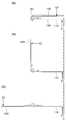
도 1은 가요성 부품을 지지하기 위한 지지구를 설명하는 사시도.
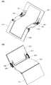
도 2는 가요성 부품을 지지하기 위한 지지구를 설명하는 상면도 및 단면도.
도 3은 가요성 부품을 지지하기 위한 지지구를 설명하는 상면도 및 단면도.
도 4는 가요성 부품을 지지하기 위한 지지구를 설명하는 단면도.
도 5는 가요성 부품을 지지하기 위한 지지구를 설명하는 단면도.
도 6은 가요성 부품을 지지하기 위한 지지구를 설명하는 사시도.
도 7은 가요성 부품을 지지하기 위한 지지구를 설명하는 상면도 및 단면도.
도 8은 가요성 부품을 지지하기 위한 지지구를 설명하는 상면도 및 단면도.
도 9는 가요성 부품을 지지하기 위한 지지구를 설명하는 단면도.
도 10은 발광 패널을 설명하는 도면.
도 11은 발광 패널을 설명하는 도면.
도 12는 발광 패널을 설명하는 도면.
도 13은 발광 패널을 설명하는 도면.
도 14는 발광 패널의 제작 방법을 설명하는 도면.
도 15는 발광 패널의 제작 방법을 설명하는 도면.
도 16은 톱니바퀴를 설명하는 도면.1 is a perspective view illustrating a support for supporting a flexible part;
2 is a top view and a cross-sectional view illustrating a support for supporting a flexible part;
3 is a top view and a cross-sectional view illustrating a support for supporting a flexible part;
Fig. 4 is a cross-sectional view illustrating a support for supporting a flexible part;
Fig. 5 is a cross-sectional view illustrating a support for supporting a flexible part;
Fig. 6 is a perspective view illustrating a support for supporting a flexible part;
7 is a top view and a cross-sectional view illustrating a support for supporting a flexible part;
8 is a top view and a cross-sectional view illustrating a support for supporting a flexible part;
Fig. 9 is a cross-sectional view illustrating a support for supporting a flexible part;
Fig. 10 is a view for explaining a light emitting panel;
11 is a view for explaining a light emitting panel;
Fig. 12 is a view for explaining a light emitting panel;
Fig. 13 is a view for explaining a light emitting panel;
Fig. 14 is a view for explaining a method of manufacturing a light emitting panel;
Fig. 15 is a view for explaining a method of manufacturing a light emitting panel;
16 is a view for explaining a gear wheel.
실시형태에 대하여 도면을 참조하여 자세히 설명한다. 다만, 본 발명은 이하의 설명에 한정되지 않으며, 본 발명의 취지 및 그 범위로부터 벗어나지 않고 그 형태 및 상세한 사항을 다양하게 변경할 수 있는 것은 당업자에게 용이하게 이해될 수 있을 것이다. 따라서, 본 발명은 이하에 기재되는 실시형태의 내용에 한정하여 해석되는 것은 아니다. 또한, 이하에서 설명하는 발명의 구성에 있어서, 동일 부분 또는 같은 기능을 갖는 부분에는 동일한 부호를 다른 도면들에 공통적으로 이용하며, 그 반복되는 설명은 생략하는 경우가 있다.EMBODIMENT OF THE INVENTION Embodiment is demonstrated in detail with reference to drawings. However, the present invention is not limited to the following description, and it will be readily understood by those skilled in the art that various changes can be made in form and detail without departing from the spirit and scope of the present invention. Therefore, this invention is limited to the content of embodiment described below and is not interpreted. In addition, in the configuration of the invention described below, the same reference numerals are commonly used in different drawings for the same parts or parts having the same functions, and repeated descriptions thereof are sometimes omitted.
(실시형태 1)(Embodiment 1)
본 실시형태에서는 본 발명의 일 형태에 따른 가요성 부품의 지지구에 대하여 설명한다. 또한, 본 발명의 일 형태에 따른 지지구는 굴곡에 대해 민감한 부품 전반에 사용할 수 있으며, 상기 부품은 전기 부품에 한정되지 않는다.In this embodiment, the support tool of the flexible component which concerns on one Embodiment of this invention is demonstrated. In addition, the support according to one embodiment of the present invention can be used in all parts sensitive to bending, and the parts are not limited to electric parts.
도 1은 본 발명의 일 형태에 따른 개폐 가능한 가요성 부품의 지지구가 경첩이 둔각을 이루도록 펼쳐진 상태의 사시도이다. 또한, 도 2의 (A), (B), (C), (D)는 가요성 부품이 평탄하게 되도록 지지구가 펼쳐진 상태를 도시한 것이다. 도 2의 (A)는 상면도(가요성 부품이 설치된 측)이고, 도 2의 (B)는 도 2의 (A)에 도시된 A1-A2 부분의 단면도이고, 도 2의 (C)는 A3-A4 부분의 단면도이고, 도 2의 (D)는 A5-A6 부분의 단면도이다.1 is a perspective view illustrating a state in which a support for an openable and openable flexible part according to an embodiment of the present invention is unfolded so that a hinge forms an obtuse angle. In addition, (A), (B), (C), and (D) of Fig. 2 show a state in which the support is unfolded so that the flexible part is flat. Fig. 2(A) is a top view (the side on which the flexible part is installed), Fig. 2(B) is a cross-sectional view of portions A1-A2 shown in Fig. 2(A), and Fig. 2(C) is It is a cross-sectional view of portion A3-A4, and FIG. 2D is a cross-sectional view of portion A5-A6.
본 발명의 일 형태에 따른 가요성 부품의 지지구는 제 1 기판(110), 제 2 기판(120), 경첩(130), 랙(150), 피니언(160)을 구비한다. 또한, 도 2의 (A)는 제 1 기판(110)과 제 2 기판(120)을 A1-A2(도면 중 상하 방향을 분할하는 중심선)를 대칭축으로 하여 선대칭 위치에 배치된 2개의 경첩으로 연결시키는 구성을 도시한 것이다. 상기 2개의 경첩은 경상(鏡像)의 관계이며, 그 이외의 구성은 마찬가지이다. 따라서, 이하에서 경첩 등을 설명할 때는 한쪽 경첩만을 자세히 설명하기로 한다.The flexible component support according to one embodiment of the present invention includes a
랙(150)은 제 1 기판(110)상의 모서리부에 고정되고, 피니언(160)은 경첩(130)의 축(140)에 중심이 고정된다. 또한, 축(140)은 경첩(130)의 경첩편(132)에 고정된다. 즉, 경첩편(132)의 동작이 축(140)을 통하여 피니언(160)에 전달된다.The
제 2 기판(120)을 제 1 기판(110)의 랙(150)이 고정된 모서리부 측에 인접시킨 상태로 하고, 랙(150)의 톱니와 피니언(160)의 톱니가 서로 맞물리도록(도 2의 (D) 참조), 제 1 기판(110) 및 제 2 기판(120) 위에 경첩(130)이 배치된다.The
경첩(130)의 경첩편(131)에는 슬라이드 기구가 제공되고, 제 1 기판(110)과 경첩(130)의 경첩편(131)은, 제 1 기판(110)이 경첩(130)의 경첩편(131)과 중첩된 상태에서 상기 슬라이드 기구에 의하여 수평 방향으로 이동할 수 있도록 서로 고정된다(도 2의 (C) 참조). 그리고, 제 2 기판(120)과 경첩(130)의 경첩편(132)이 고정된다.A slide mechanism is provided on the
본 발명의 일 형태에 있어서, 상기 슬라이드 기구의 구성에 제한은 없다. 예를 들어, 도면에 도시된 바와 같이 경첩(130)의 경첩편(131)에 형성된 가는 구멍(170)과, 상기 가는 구멍에 삽입되고 제 1 기판에 고정되는 지그(180)(나사 등)로 구성될 수 있다. 또한, 상기 가는 구멍은 제 1 기판 측에 형성되어도 좋다. 또한, 상기 슬라이드 기구로서, 상하의 테이블이 베어링이나 저마찰 재료 등을 개재하여 중첩된 기구 등을 사용할 수도 있다.In one embodiment of the present invention, there is no restriction on the configuration of the slide mechanism. For example, as shown in the drawing, a thin hole 170 formed in the
또한, 경첩(130)의 경첩편(131)에 2개의 가는 구멍(170)이 형성된 예를 도시하였지만, 하나의 가는 구멍(170)을 형성하여도 좋다.In addition, although an example in which two fine holes 170 are formed in the
또한, 가요성 부품(190)은 도 2의 (A), (B)에 도시된 영역 F1 이외의 영역을 제 1 기판(110) 및 제 2 기판(120)에 고정할 수 있다. 영역 F1은 가요성 부품(190)을 구부릴 수 있는 영역에 상당하며, 영역 F1에서 제 1 기판(110)과 가요성 부품(190)은 고정되지 않도록 할 필요가 있다.Also, the
도 3의 (A), (B), (C), (D)는 도 1에 도시된 지지구가 닫힌 상태를 도시한 것이다. 도 3의 (A)는 상면도이고, 도 3의 (B)는 도 3의 (A) 중 B1-B2 부분의 단면도이고, 도 3의 (C)는 B3-B4 부분의 단면도이고, 도 3의 (D)는 B5-B6 부분의 단면도이다.(A), (B), (C), and (D) of FIG. 3 illustrate a closed state of the support shown in FIG. 1 . 3A is a top view, FIG. 3B is a cross-sectional view of part B1-B2 of FIG. 3A, FIG. 3C is a cross-sectional view of part B3-B4, and FIG. 3 (D) is a cross-sectional view of part B5-B6.
상기 구성의 지지구에 있어서, 제 2 기판(120)을 이동시킴으로써, 피니언(160)의 회전력을 랙(150)에 전달시켜, 제 1 기판(110)을 경첩(130)의 경첩편(131)과 중첩된 상태에서 수평 방향으로 이동시킬 수 있다. 또한, 제 1 기판(110) 또는 양쪽 기판의 이동에 의해서도 상기와 같은 동작이 가능하다.In the support of the above configuration, by moving the
따라서, 도 2의 (B)에 도시된 바와 같이, 가요성 부품(190)이 제 1 기판(110) 및 제 2 기판(120)에 고정된 상태이어도 도 3의 (B)에 도시된 바와 같이 구부러지는 부분의 곡률 반경을 일정하게 유지한 채 지지구를 구부릴 수 있다. 또한, 가요성 부품(190)의 구부러지는 부분의 허용 곡률 반경은 경첩(130)의 축(140)을 덮는 관의 직경 및 피니언(160)의 직경을 선택함으로써 조정할 수 있다.Therefore, as shown in FIG. 2B , even when the
또한, 도 4의 (A), (B), (C)는 본 발명의 일 형태에 따른 지지구를 닫은 상태로부터 펼친 상태로 하기까지의 과정을 도시한 측면도이다. 여기서, 가요성 부품(190)의 제 1 기판(110) 측의 단부를 E1, 제 2 기판(120) 측의 단부를 E2로 하였을 때, 개폐 동작을 수행하여도 단부 E1 및 단부 E2의 위치가 변화되지 않는 것을 알 수 있다.4(A), (B), and (C) are side views showing the process from the closed state to the unfolded state of the support tool according to one embodiment of the present invention. Here, when the end of the
즉, 본 발명의 일 형태에 따른 지지구에서는, 가요성 부품(190) 중 구부러지는 부분 이외의 부분을 제 1 기판(110) 및 제 2 기판(120)에 고정할 수 있다. 따라서, 가요성 부품(190)에 강한 기계적 강도를 부여할 수 있기 때문에 신뢰성을 향상시킬 수 있다. 또한, 제 1 기판(110) 및 제 2 기판(120)의 면 형상을 가요성 부품(190)에 반영시킬 수 있기 때문에, 기능성이나 디자인성을 향상시킬 수 있다. 예를 들어, 가요성 부품(190)이 표시 장치인 경우, 제 1 기판(110) 및 제 2 기판(120)의 면 형상을 평탄하게 함으로써 시인성을 향상시킬 수 있다.That is, in the support tool according to one embodiment of the present invention, portions other than the bent portion of the
한편, 도 5는 본 발명의 일 형태를 사용하지 않는 비교예인 지지구의 개폐 동작을 도시한 것이다. 도 5의 (A), (B), (C)는 지지구를 닫은 상태로부터 펼친 상태로 하기까지의 과정을 도시한 측면도이다. 도 5에 도시된 지지구는 랙, 피니언, 및 슬라이드 기구를 구비하지 않고, 제 1 기판(110)이 수평 방향으로 이동할 수 없다는 점이 본 발명의 일 형태와 다르다.On the other hand, FIG. 5 shows the opening/closing operation of the support, which is a comparative example that does not use one embodiment of the present invention. 5 (A), (B), and (C) are side views showing the process from the closed state to the unfolded state of the support. The support shown in FIG. 5 is different from one embodiment of the present invention in that it does not include a rack, a pinion, and a slide mechanism, and the
도 5에 도시된 지지구에서, 가요성 부품(190)은 제 1 기판(110)에 고정하고 제 2 기판(120)에는 고정하지 않는 상태로 한다. 이 때, 개폐 동작에 있어서, 가요성 부품(190)의 단부 E1의 위치는 변화되지 않지만, 단부 E2의 위치는 개폐의 정도에 따라 변화된다.In the support shown in FIG. 5 , the
이것은 도 5의 (A)에 도시된 바와 같이 가요성 부품(190)의 일부의 영역(191)이 구부러지는 부분으로서 사용되기 때문이다. 도 5의 (B)에 도시된 형태로부터 도 5의 (A)에 도시된 형태로 변화시키면, 제 2 기판(120) 위에서 가요성 부품(190)이 경첩 쪽으로 이끌리도록 이동하여 단부 E2의 위치가 변화된다. 또한, 도 5의 (B)에 도시된 형태로부터 도 5의 (C)에 도시된 형태로 변화시키면, 제 2 기판(120) 위에서 가요성 부품(190)이 경첩과 반대 쪽으로 이동하여, 단부 E2의 위치가 변화된다.This is because the
따라서, 도 5에 도시된 지지구에서는 제 2 기판(120)에 가요성 부품(190)을 고정할 수 없기 때문에, 기계적 강도를 향상시키기 어렵다. 또한, 제 2 기판(120)과 가요성 부품 사이에서 마찰이 발생하기 때문에 기계적 또는 전기적 신뢰성이 저하될 수 있다. 또한, 제 2 기판(120)의 면 형상을 가요성 부품(190)에 반영할 수 없기 때문에, 기능성이나 디자인성을 충분히 향상시키기 어렵다.Accordingly, in the support shown in FIG. 5 , since the
그러므로 본 발명의 일 형태를 사용함으로써, 가요성 부품에 우수한 신뢰성, 기능성, 및 디자인성을 부여할 수 있다.Therefore, by using one embodiment of the present invention, excellent reliability, functionality, and design properties can be imparted to flexible parts.
또한, 본 명세서에서 설명하는 톱니바퀴나 경첩 등의 부품은 일례에 불과하며, 그 형상이나 개수 등에 제한은 없다. 또한, 본 명세서에서 설명하는 톱니바퀴나 경첩이 갖는 작용과 같은 작용을 갖는 다른 부품을 상기 톱니바퀴 및 상기 경첩 대신에 사용할 수도 있다.In addition, the parts, such as a gear wheel or a hinge, which are described in this specification are only an example, and there is no limitation on the shape, number, etc. In addition, other parts having the same action as that of a gear wheel or a hinge described herein may be used instead of the gear wheel and the hinge.
본 실시형태는 다른 실시형태에 기재된 구성과 적절히 조합하여 실시할 수 있다.This embodiment can be implemented in appropriate combination with the structures described in other embodiments.
(실시형태 2)(Embodiment 2)
본 실시형태에서는 실시형태 1과 다른 본 발명의 일 형태에 따른 가요성 부품의 지지구에 대하여 설명한다. 실시형태 1에서는 한 번 접히는 지지구를 설명하였지만, 본 실시형태에서는 두 번 접히는 지지구에 대하여 설명한다.In this embodiment, the support tool of the flexible component which concerns on one Embodiment of this invention different from Embodiment 1 is demonstrated. In Embodiment 1, the support tool folded once is described, but in this embodiment, the support tool folded twice will be described.
도 6의 (A), (B)는 본 발명의 일 형태에 따른 개폐 동작이 가능한 가요성 부품의 지지구에서 각 경첩이 둔각을 이루도록 펼친 상태를 도시한 사시도이다. 도 6의 (A)는 가요성 부품이 설치된 측이며, 도 6의 (B)는 도 6의 (A)의 반대측이다. 또한, 도 7의 (A), (B), (C), (D)는 본 발명의 일 형태에 따른 개폐 가능한 가요성 부품의 지지구가 펼쳐진 상태를 도시한 것이다. 도 7의 (A)는 상면도(가요성 부품이 설치된 측)이고, 도 7의 (B)는 도 7의 (A)에 도시된 C1-C2 부분의 단면도이고, 도 7의 (C)는 C3-C4 부분의 단면도이고, 도 7의 (D)는 C5-C6 부분의 단면도이다.6A and 6B are perspective views illustrating a state in which each hinge is unfolded to form an obtuse angle in a support for a flexible part capable of opening/closing operation according to an embodiment of the present invention. Fig. 6(A) is the side on which the flexible part is installed, and Fig. 6(B) is the opposite side to Fig. 6(A). 7(A), (B), (C), and (D) show a state in which the support of the openable and openable flexible part according to one embodiment of the present invention is unfolded. Fig. 7(A) is a top view (the side on which the flexible part is installed), Fig. 7(B) is a cross-sectional view of part C1-C2 shown in Fig. 7(A), and Fig. 7(C) is It is a cross-sectional view of part C3-C4, and FIG. 7D is a cross-sectional view of part C5-C6.
본 발명의 일 형태에 따른 가요성 부품의 지지구는 제 1 기판(211), 제 2 기판(212), 제 3 기판(213), 제 1 경첩(220), 제 1 랙(251), 제 2 랙(252), 제 1 피니언(261), 제 2 피니언(262), 제 3 피니언(263), 및 중간 톱니바퀴(264)를 구비한다. 또한, 도 7의 (A)는 제 1 기판(211), 제 2 기판(212), 및 제 3 기판(213)을 C1-C2(도면 중 상하 방향을 분할하는 중심선)를 대칭축으로 하여 선대칭 위치에 배치된 2쌍(총 4개)의 경첩으로 접속시키는 구성을 도시한 것이다. 제 1 기판(211)과 제 2 기판(212)을 접속하는 2개의 경첩은 경상의 관계이며, 그 이외의 구성은 마찬가지이다. 또한, 제 2 기판(212)과 제 3 기판(213)을 접속하는 2개의 경첩은 경상의 관계이며, 그 이외의 구성은 마찬가지이다. 따라서, 이하에서 종류가 같은 경첩 등을 설명할 때는 한쪽 경첩만을 자세히 설명하기로 한다.The flexible component support according to one embodiment of the present invention includes a
제 1 랙(251)은 제 2 기판(212)상의 모서리부에 고정되고, 제 1 피니언(261)은 제 1 경첩(220)의 축(241)에 중심이 고정된다. 또한, 축(241)은 제 1 경첩(220)의 경첩편(221)에 고정된다. 즉, 제 1 피니언(261)에는 경첩편(221)의 동작이 축(241)을 통하여 전달된다.The
제 1 기판(211)을 제 2 기판(212)의 제 1 랙(251)이 고정된 모서리부 측에 인접시킨 상태로 하고, 제 1 랙(251)의 톱니와 제 1 피니언(261)의 톱니가 서로 맞물리도록(도 7의 (D) 참조), 제 1 기판(211) 및 제 2 기판(212) 위에 제 1 경첩(220)이 배치된다.The
제 1 경첩(220)의 경첩편(222)에는 제 1 슬라이드 기구가 제공되고, 제 2 기판(212)과 제 1 경첩(220)의 경첩편(222)은, 제 2 기판(212)이 제 1 경첩(220)의 경첩편(222)과 중첩된 상태에서 상기 제 1 슬라이드 기구에 의하여 수평 방향으로 이동할 수 있도록 서로 고정된다(도 7의 (C) 참조). 그리고, 제 1 기판(211)과 제 1 경첩(220)의 경첩편(221)이 고정된다.The
본 발명의 일 형태에 있어서, 상기 제 1 슬라이드 기구의 구성에 제한은 없다. 예를 들어, 도면에 도시된 바와 같이 제 1 경첩(220)의 다른 쪽 경첩편(222)에 형성된 가는 구멍(271)과, 상기 가는 구멍에 삽입된 지그(280)(나사 등)로 구성될 수 있다. 또한, 제 1 슬라이드 기구에 관해서는 실시형태 1에 제시된 슬라이드 기구의 설명을 참조할 수 있다.In one embodiment of the present invention, there is no restriction on the configuration of the first slide mechanism. For example, as shown in the drawing, a
또한, 제 1 경첩(220)의 경첩편(222)에 2개의 가는 구멍(271)이 형성된 예를 도시하였지만, 하나의 가는 구멍(271)을 형성하여도 좋다.In addition, although an example in which two
또한, 가요성 부품(290)은 도 7의 (A), (B)에 도시된 영역 F2 이외의 영역을 제 1 기판(211), 제 2 기판(212), 및 제 3 기판(213)에 고정할 수 있다. 영역 F2는 가요성 부품(290)을 구부릴 수 있는 영역에 상당하며, 영역 F2에서 제 2 기판(212)과 가요성 부품(290)은 고정되지 않도록 할 필요가 있다.In addition, the
제 2 랙(252)은 제 3 기판(213)상의 모서리부에 고정되고, 제 2 피니언(262)은 제 2 경첩(230)의 경첩편(232)에 고정된 축(242)에 중심이 고정된다. 또한, 제 3 피니언(263)은 제 2 경첩(230)의 경첩편(231)에 고정된 축(243)에 중심이 고정된다. 그리고, 제 2 피니언(262) 및 제 3 피니언(263)은 중간 톱니바퀴(264)를 개재하여 톱니가 서로 맞물린다. 또한, 중간 톱니바퀴는 제 2 경첩(230)의 경첩편(232)에 고정된 축에 중심이 고정된다. 이 구성에 의하여, 경첩편(231)의 동작이 축(243)을 통하여 제 3 피니언(263)에 전달되고, 제 3 피니언(263)의 동작은 중간 톱니바퀴(244)를 통하여 제 2 피니언(262)에 전달된다.The
제 2 기판(212)의 제 1 경첩(220)을 고정한 측과는 반대측을, 제 3 기판(213)의 제 2 랙(252)이 고정된 모서리부 측에 인접시킨 상태로 하고, 제 2 랙(252)의 톱니와 제 2 피니언(262)의 톱니가 서로 맞물리도록(도 7의 (D) 참조) 제 2 기판(212) 및 제 3 기판(213) 위에 제 2 경첩(230)이 배치된다.The side opposite to the side to which the
제 2 경첩(230)의 경첩편(232)에는 제 2 슬라이드 기구가 제공되고, 제 3 기판(213)과 제 2 경첩(230)의 경첩편(232)은, 제 3 기판(213)이 제 2 경첩(230)의 경첩편(232)과 중첩된 상태에서 상기 제 2 슬라이드 기구에 의하여 수평 방향으로 이동할 수 있도록 서로 고정된다(도 7의 (C) 참조). 그리고, 제 2 기판(212)과 제 2 경첩(230)의 경첩편(231)이 고정된다.A second slide mechanism is provided on the
본 발명의 일 형태에 있어서, 상기 제 2 슬라이드 기구의 구성에 제한은 없다. 예를 들어, 도면에 도시된 바와 같이 제 2 경첩(230)의 경첩편(232)에 형성된 가는 구멍(272)과, 상기 가는 구멍에 삽입된 지그(280)(나사 등)로 구성될 수 있다. 또한, 제 2 슬라이드 기구에 관해서는 실시형태 1에 제시된 슬라이드 기구의 설명을 참조할 수 있다.In one embodiment of the present invention, there is no restriction on the configuration of the second slide mechanism. For example, as shown in the drawing, it may be composed of a
또한, 제 2 경첩(230)의 경첩편(232)에 하나의 가는 구멍(272)이 형성된 예를 도시하였지만, 2개의 가는 구멍(272)을 형성하여도 좋다.Further, although an example in which one
또한, 제 3 기판(213)에는 제 4 기판(214)이 고정되어 있고, 가요성 부품(290)은 실제로는 제 4 기판(214)에 고정된다. 다만, 제 3 기판(213)과 제 4 기판(214)을 하나의 동일한 기판으로 하면, 가요성 부품(290)은 제 3 기판(213)에 고정되는 것으로 하여 설명할 수 있다.Further, a
또한, 접었을 때, 제 2 피니언(262), 제 3 피니언(263), 및 중간 톱니바퀴(264)가 서로 간섭되지 않도록 제 2 기판(212)의 모서리부에는 절단된 부분이 제공되어 있다.In addition, cut-off portions are provided at the corners of the
또한, 도 7은 제 2 경첩(230)의 경첩편(231)이 제 2 기판(212)과 일체로 형성된 예이지만, 상술한 바와 같이 경첩편(231)을 제 2 기판(212)에 고정하는 구성이어도 좋다.7 is an example in which the
또한, 제 2 피니언(262), 제 3 피니언(263), 및 중간 톱니바퀴(264)는 도 16과 같은 구성이어도 좋다. 도 16의 (A)는 상면도이고 도 16의 (B)는 측면도이다.In addition, the
제 3 피니언(263)은 톱니바퀴(263a) 및 톱니바퀴(263b)를 구비한다. 제 2 피니언(262) 및 톱니바퀴(263b)는 중간 톱니바퀴(264)를 개재하여 서로 맞물린다. 또한, 제 2 랙(252)은 톱니바퀴(263a)와만 맞물리는 구성이다.The
도 8의 (A), (B), (C), (D)는 도 6에 도시된 지지구가 닫힌 상태를 도시한 것이다. 도 8의 (A)는 상면도이고, 도 8의 (B)는 도 8의 (A) 중 D1-D2 부분의 단면도이고, 도 8의 (C)는 D3-D4 부분의 단면도이고, 도 8의 (D)는 D5-D6 부분의 단면도이다.(A), (B), (C), and (D) of Figure 8 illustrate a closed state of the support shown in Figure 6 . Fig. 8(A) is a top view, Fig. 8(B) is a cross-sectional view of part D1-D2 in Fig. 8(A), Fig. 8(C) is a cross-sectional view of part D3-D4, and Fig. 8 (D) is a cross-sectional view of part D5-D6.
상기 구성의 지지구에 있어서, 제 1 기판(211)을 이동시킴으로써, 제 1 피니언(261)의 회전력을 제 1 랙(251)에 전달시켜, 제 2 기판(212)을 제 1 경첩(220)의 경첩편(222)과 중첩된 상태에서 수평 방향으로 이동시킬 수 있다.In the support of the above configuration, by moving the
또한, 제 2 기판(212)을 이동시킴으로써, 제 3 피니언(263)의 회전력을 중간 톱니바퀴(264) 및 제 2 피니언(262)을 통하여 제 2 랙(252)에 전달시켜, 제 3 기판(213)을 제 2 경첩(230)의 한쪽 경첩편(232)과 중첩된 상태에서 수평 방향으로 이동시킬 수 있다. 또한, 기판을 이동시키는 동작은 지지구의 개폐 동작이며, 상기 개폐 동작은 어느 기판의 이동에 의해서도 가능하다.In addition, by moving the
따라서, 도 7의 (B)에 도시된 바와 같이 가요성 부품(290)이 제 1 기판(211), 제 2 기판(212), 및 제 3 기판(213)(제 4 기판(214))에 고정된 상태이어도 도 8의 (B)에 도시된 바와 같이 구부러지는 부분의 곡률 반경을 일정하게 유지한 채 지지구를 구부릴 수 있다. 또한, 가요성 부품(290)의 구부러지는 부분의 허용 곡률 반경은 제 1 경첩(220)의 축(241)을 덮는 관의 직경, 제 1 피니언(261)의 직경, 제 2 경첩(230)의 축(243)을 덮는 관의 직경, 및 제 3 피니언(263)의 직경을 선택함으로써 조정할 수 있다.Accordingly, as shown in FIG. 7B , the
또한, 도 9의 (A), (B), (C), (D)는 본 발명의 일 형태에 따른 지지구를 닫은 상태로부터 펼친 상태로 하기까지의 과정을 도시한 측면도이다. 또한, 제 3 기판(213)의 일부를 투과시켜 도시하였다. 여기서, 가요성 부품(290)의 제 1 기판(211) 측의 단부를 E1, 제 3 기판(213) 측의 단부를 E2로 하였을 때, 개폐 동작을 수행하여도 단부 E1 및 단부 E2의 위치가 변화되지 않는 것을 알 수 있다.9(A), (B), (C), and (D) are side views showing the process from the closed state to the unfolded state of the support tool according to one embodiment of the present invention. In addition, a portion of the
즉, 본 발명의 일 형태에 따른 지지구는 가요성 부품(290)이 제 1 기판(211), 제 2 기판(212), 및 제 3 기판(213)(제 4 기판(214))에 고정된 상태이기 때문에, 가요성 부품(290)에 강한 기계적 강도를 부여할 수 있어 신뢰성을 향상시킬 수 있다. 또한, 제 1 기판(211), 제 2 기판(212), 및 제 3 기판(213)(제 4 기판(214))의 면 형상을 가요성 부품(290)에 반영시킬 수 있으며, 기능성이나 디자인성을 향상시킬 수 있다. 예를 들어, 가요성 부품(290)이 표시 장치인 경우, 제 1 기판(211), 제 2 기판(212), 및 제 3 기판(213)(제 4 기판(214))의 면 형상을 평탄하게 함으로써 시인성을 향상시킬 수 있다.That is, in the support according to one embodiment of the present invention, the
따라서, 본 발명의 일 형태를 사용함으로써, 가요성 부품에 우수한 신뢰성, 기능성, 및 디자인성을 부여할 수 있다. 또한, 본 발명의 일 형태를 사용함으로써, 가요성 부품을 작게 접을 수 있어, 가요성 부품의 휴대성을 우수하게 할 수 있다.Therefore, by using one embodiment of the present invention, it is possible to impart excellent reliability, functionality, and design properties to flexible parts. Moreover, by using one aspect of this invention, a flexible component can be folded small, and it can make it excellent in portability of a flexible component.
본 실시형태는 다른 실시형태에 기재된 구성과 적절히 조합하여 실시할 수 있다.This embodiment can be implemented in appropriate combination with the structures described in other embodiments.
(실시형태 3)(Embodiment 3)
본 실시형태에서는 실시형태 1 및 실시형태 2에서 설명한 가요성 부품으로서 사용할 수 있는 발광 장치(발광 패널)의 예에 대하여 설명한다.In this embodiment, the example of the light emitting device (light emitting panel) which can be used as a flexible component demonstrated in Embodiment 1 and Embodiment 2 is demonstrated.
<구체예 1><Specific Example 1>
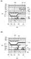
도 10의 (A)는 가요성 부품의 일례로서 사용할 수 있는 발광 패널의 평면도이고, 도 10의 (B)는 도 10의 (A) 중 일점 쇄선 G1-G2 부분의 단면도의 일례이다.Fig. 10A is a plan view of a light emitting panel that can be used as an example of a flexible component, and Fig. 10B is an example of a cross-sectional view taken along the dash-dotted line G1-G2 in Fig. 10A.
도 10의 (B)에 도시된 발광 패널은 소자층(301), 접착층(305), 기판(303)을 구비한다. 소자층(301)은 기판(401), 접착층(403), 절연층(405), 트랜지스터(440), 도전층(357), 절연층(407), 절연층(409), 발광 소자(430), 절연층(411), 밀봉층(413), 절연층(461), 착색층(459), 차광층(457), 및 절연층(455)을 구비한다.The light emitting panel shown in FIG. 10B includes an
도전층(357)은 접속체(415)를 개재하여 FPC(308)에 전기적으로 접속된다.The
발광 소자(430)는 하부 전극(431), EL층(433), 및 상부 전극(435)을 구비한다. 하부 전극(431)은 트랜지스터(440)의 소스 전극 또는 드레인 전극에 전기적으로 접속된다. 하부 전극(431)의 단부는 절연층(411)으로 덮여 있다. 발광 소자(430)는 전면 발광(top emission) 구조이다. 상부 전극(435)은 투광성을 가지며 EL층(433)이 발광한 광을 투과시킨다.The
발광 소자(430)와 중첩되는 위치에 착색층(459)이 제공되고 절연층(411)과 중첩되는 위치에 차광층(457)이 제공된다. 착색층(459) 및 차광층(457)은 절연층(461)으로 덮여 있다. 발광 소자(430)와 절연층(461) 사이는 밀봉층(413)으로 충전되어 있다.A
발광 패널은 광 추출부(304) 및 구동 회로부(306)에 복수의 트랜지스터를 구비한다. 트랜지스터(440)는 절연층(405) 위에 제공된다. 절연층(405)과 기판(401)은 접착층(403)에 의하여 접합된다. 또한, 절연층(455)과 기판(303)은 접착층(305)에 의하여 접합된다. 절연층(405)이나 절연층(455)에 투수성이 낮은 막을 사용하면, 발광 소자(430)나 트랜지스터(440)에 물 등 불순물이 침입되는 것을 억제할 수 있기 때문에 발광 패널의 신뢰성이 높아져 바람직하다. 접착층(403)에는 접착층(305)과 같은 재료를 사용할 수 있다.The light emitting panel includes a plurality of transistors in the
구체예 1에서는 내열성이 우수한 제작 기판 위에 절연층(405), 트랜지스터(440), 발광 소자(430)를 제작하고, 상기 제작 기판을 박리하고 접착층(403)을 사용하여 기판(401) 위에 절연층(405), 트랜지스터(440), 발광 소자(430)를 적재함으로써 제작할 수 있는 발광 패널을 제시한다. 또한, 구체예 1에서는 내열성이 우수한 제작 기판 위에 절연층(455), 착색층(459), 및 차광층(457)을 제작하고, 상기 제작 기판을 박리하고, 접착층(305)을 사용하여 기판(303) 위에 절연층(455), 착색층(459), 및 차광층(457)을 적재함으로써 제작할 수 있는 발광 패널을 제시한다.In Specific Example 1, an insulating
기판에 투수성이 높고 내열성이 낮은 재료(수지 등)를 사용하는 경우, 제작 공정에서 기판을 고온으로 가열할 수 없기 때문에 상기 기판 위에 트랜지스터나 절연막을 제작하는 조건이 제한된다. 본 실시형태에 따른 제작 방법에서는 내열성이 높은 제작 기판 위에서 트랜지스터 등을 제작할 수 있기 때문에 신뢰성이 높은 트랜지스터나 투수성이 충분히 낮은 절연막을 형성할 수 있다. 그리고, 이들을 기판(303)이나 기판(401)으로 이동시켜 적재함으로써, 신뢰성이 높은 발광 패널을 제작할 수 있다. 그러므로, 본 발명의 일 형태에 따르면 가볍거나 얇으며 신뢰성이 높은 발광 장치를 실현할 수 있다. 제작 방법에 관해서는 나중에 자세히 설명한다.When a material (resin, etc.) having high water permeability and low heat resistance is used for the substrate, the conditions for manufacturing the transistor or insulating film on the substrate are limited because the substrate cannot be heated to a high temperature in the manufacturing process. In the manufacturing method according to the present embodiment, since a transistor or the like can be manufactured on a substrate having high heat resistance, a highly reliable transistor or an insulating film with sufficiently low water permeability can be formed. Then, by moving these onto the
기판(303) 및 기판(401)에는 각각 인성(靭性)이 높은 재료를 사용하는 것이 바람직하다. 이로써, 내충격성이 우수하고 파손되기 어려운 표시 장치를 실현할 수 있다. 예를 들어, 기판(303)으로서 유기 수지 기판을 사용하고, 기판(401)으로서 두께가 얇은 금속 재료나 합금 재료를 사용한 기판을 사용함으로써 기판으로서 유리 기판을 사용하는 경우에 비하여 가볍고 파손되기 어려운 발광 패널을 구현할 수 있다.It is preferable to use a material having high toughness for the
금속 재료나 합금 재료는 열 전도성이 높아 기판 전체에 열을 용이하게 전도할 수 있기 때문에, 발광 패널의 국소적인 온도 상승을 억제할 수 있어 바람직하다. 금속 재료나 합금 재료를 사용한 기판의 두께는 10μm 이상 200μm 이하가 바람직하고, 20μm 이상 50μm 이하이면 더 바람직하다.A metallic material or an alloy material is preferable because it can suppress a local temperature rise of a light emitting panel since it can conduct heat easily to the whole board|substrate with high thermal conductivity. 10 micrometers or more and 200 micrometers or less are preferable and, as for the thickness of the board|substrate using a metal material or alloy material, it is more preferable in it being 20 micrometers or more and 50 micrometers or less.
또한, 기판(401)에 열 방사율이 높은 재료를 사용하면 발광 패널의 표면 온도가 높아지는 것을 억제할 수 있어 발광 패널의 파손이나 신뢰성 저하를 억제할 수 있다. 예를 들어, 기판(401)을 금속 기판과 열 방사율이 높은 층(예를 들어, 금속 산화물이나 세라믹 재료를 사용할 수 있음)을 포함한 적층 구조로 하여도 좋다.In addition, when a material having a high thermal emissivity is used for the
<구체예 2><Specific Example 2>
도 11의 (A)는 발광 패널의 광 추출부(304)의 다른 일례이다. 도 11의 (A)의 발광 패널은 터치 조작이 가능한 발광 패널이다. 또한, 이하에 기재되는 각 구체예에서는 구체예 1과 같은 구성에 관한 설명은 생략하기로 한다.11A is another example of the
도 11의 (A)에 도시된 발광 패널은 소자층(301), 접착층(305), 기판(303)을 구비한다. 소자층(301)은 기판(401), 접착층(403), 절연층(405), 트랜지스터(440), 절연층(407), 절연층(409), 발광 소자(430), 절연층(411), 절연층(417), 밀봉층(413), 절연층(461), 착색층(459), 차광층(457), 수광 소자, 도전층(481), 도전층(483), 절연층(491), 절연층(493), 절연층(495), 및 절연층(455)을 구비한다.The light emitting panel shown in FIG. 11A includes an
구체예 2에서는 절연층(411) 위에 절연층(417)을 구비한다. 절연층(417)을 제공함으로써, 기판(303)과 기판(401) 사이의 간격을 조정할 수 있다.In the second embodiment, the insulating
도 11의 (A)는 절연층(455)과 밀봉층(413) 사이에 수광 소자를 구비하는 예이다. 기판(401) 측의 비발광 영역(예를 들어, 트랜지스터(440)나 배선이 제공된 영역)과 중첩되도록 수광 소자를 배치할 수 있기 때문에 화소(발광 소자)의 개구율을 저하시키지 않으면서 발광 패널에 터치 센서를 제공할 수 있다.11A is an example in which a light-receiving element is provided between the insulating
발광 패널이 구비하는 수광 소자에는 예를 들어, PN 포토다이오드 또는 PIN 포토다이오드를 사용할 수 있다. 본 실시형태에서는 수광 소자로서 p형 반도체층(471), i형 반도체층(473), 및 n형 반도체층(475)을 구비하는 PIN 포토다이오드를 사용한다.For the light receiving element included in the light emitting panel, for example, a PN photodiode or a PIN photodiode may be used. In this embodiment, a PIN photodiode including a p-
또한, i형 반도체층(473)은 p형을 부여하는 불순물 및 n형을 부여하는 불순물을 각각 1×1020cm-3 이하의 농도로 포함하고, 암(暗) 전도도에 대한 광 전도도가 100배 이상이다. i형 반도체층(473)에는 원소 주기율표 13족 또는 15족에 속하는 불순물 원소를 갖는 것도 그 범주에 포함된다. 즉, i형 반도체는 가전자 제어를 위한 불순물 원소를 의도적으로 첨가하지 않는 경우, 약한 n형 전기 전도성을 나타내기 때문에 i형 반도체층(473)은 p형을 부여하는 불순물 원소가 성막 시 또는 성막 후에 의도적으로 또는 비의도적으로 첨가된 것이 그 범주에 포함된다.In addition, the i-
차광층(457)은 수광 소자보다 기판(303)에 가까운 측에 위치하고, 수광 소자와 중첩된다. 수광 소자와 밀봉층(413) 사이에 위치하는 차광층(457)에 의하여, 발광 소자(430)가 발광한 광이 수광 소자에 조사되는 것을 억제할 수 있다.The light-
도전층(481) 및 도전층(483)은 각각 수광 소자와 전기적으로 접속된다. 도전층(481)으로서는 수광 소자에 입사되는 광을 투과시키는 도전층을 사용하는 것이 바람직하다. 도전층(483)으로서는 수광 소자에 입사되는 광을 차광하는 도전층을 사용하는 것이 바람직하다.The
광학식 터치 센서를 기판(303)과 밀봉층(413) 사이에 제공하면 발광 소자(430)의 발광에 의한 영향을 받기 어려워지고 S/N비를 향상시킬 수 있어 바람직하다.If the optical touch sensor is provided between the
<구체예 3><Specific Example 3>
도 11의 (B)는 발광 패널의 광 추출부(304)의 다른 일례이다. 도 11의 (B)에 도시된 발광 패널은 터치 조작이 가능한 발광 패널이다.11B is another example of the
도 11의 (B)에 도시된 발광 패널은 소자층(301), 접착층(305), 기판(303)을 구비한다. 소자층(301)은 기판(401), 접착층(403), 절연층(405), 트랜지스터(440), 절연층(407), 절연층(409a), 절연층(409b), 발광 소자(430), 절연층(411), 절연층(417), 밀봉층(413), 착색층(459), 차광층(457), 수광 소자, 도전층(480), 도전층(481), 및 절연층(455)을 구비한다.The light emitting panel shown in FIG. 11B includes an
도 11의 (B)는 절연층(405)과 밀봉층(413) 사이에 수광 소자를 구비하는 예이다. 절연층(405)과 밀봉층(413) 사이에 수광 소자를 제공함으로써, 트랜지스터(440)를 구성하는 도전층이나 반도체층과 동일한 재료 및 공정으로, 수광 소자와 전기적으로 접속되는 도전층이나 수광 소자를 구성하는 광전 변환층을 제작할 수 있다. 따라서, 제작 공정을 대폭으로 증가시키지 않으면서 터치 조작이 가능한 발광 패널을 제작할 수 있다.11B is an example in which a light-receiving element is provided between the insulating
<구체예 4><Specific Example 4>
도 12의 (A)는 발광 패널의 다른 일례이다. 도 12의 (A)에 도시된 발광 패널은 터치 조작이 가능한 발광 패널이다.12A is another example of a light emitting panel. The light emitting panel shown in FIG. 12A is a light emitting panel capable of touch operation.
도 12의 (A)에 도시된 발광 패널은 소자층(301), 접착층(305), 기판(303)을 구비한다. 소자층(301)은 기판(401), 접착층(403), 절연층(405), 트랜지스터(440), 도전층(356), 도전층(357), 절연층(407), 절연층(409), 발광 소자(430), 절연층(411), 절연층(417), 밀봉층(413), 착색층(459), 차광층(457), 절연층(455), 도전층(472), 도전층(474), 절연층(476), 절연층(478), 도전층(494), 및 도전층(496)을 구비한다.The light emitting panel shown in FIG. 12A includes an
도 12의 (A)는 절연층(455)과 밀봉층(413) 사이에 정전 용량 방식의 터치 센서를 구비하는 예이다. 정전 용량 방식의 터치 센서는 도전층(472) 및 도전층(474)을 구비한다.12A is an example in which a capacitive touch sensor is provided between the insulating
도전층(356) 및 도전층(357)은 접속체(415)를 통하여 FPC(308)와 전기적으로 접속된다. 도전층(494) 및 도전층(496)은 도전성 입자(492)를 통하여 도전층(474)과 전기적으로 접속된다. 따라서, FPC(308)를 통하여 정전 용량 방식의 터치 센서를 구동시킬 수 있다.The
<구체예 5><Specific Example 5>
도 12의 (B)는 발광 패널의 다른 일례이다. 도 12의 (B)에 도시된 발광 패널은 터치 조작이 가능한 발광 패널이다.12B is another example of a light emitting panel. The light emitting panel shown in FIG. 12B is a light emitting panel capable of touch operation.
도 12의 (B)에 도시된 발광 패널은 소자층(301), 접착층(305), 및 기판(303)을 구비한다. 소자층(301)은 기판(401), 접착층(403), 절연층(405), 트랜지스터(440), 도전층(356), 도전층(357), 절연층(407), 절연층(409), 발광 소자(430), 절연층(411), 절연층(417), 밀봉층(413), 착색층(459), 차광층(457), 절연층(455), 도전층(470), 도전층(472), 도전층(474), 절연층(476), 및 절연층(478)을 구비한다.The light emitting panel shown in FIG. 12B includes an
도 12의 (B)는 절연층(455)과 밀봉층(413) 사이에 정전 용량 방식의 터치 센서를 구비하는 예이다. 정전 용량 방식의 터치 센서는 도전층(472) 및 도전층(474)을 구비한다.12B is an example in which a capacitive touch sensor is provided between the insulating
도전층(356) 및 도전층(357)은 접속체(415a)를 통하여 FPC(308a)와 전기적으로 접속된다. 도전층(470)은 접속체(415b)를 통하여 FPC(308b)와 전기적으로 접속된다. 따라서, FPC(308a)를 통하여 발광 소자(430)나 트랜지스터(440)를 구동시키고, FPC(308b)를 통하여 정전 용량 방식의 터치 센서를 구동시킬 수 있다.The
<구체예 6><Specific Example 6>
도 13의 (A)는 발광 패널의 광 추출부(304)의 다른 일례이다.13A is another example of the
도 13의 (A)에 도시된 광 추출부(304)는 기판(303), 접착층(305), 기판(402), 절연층(405), 트랜지스터(440), 절연층(407), 도전층(408), 절연층(409a), 절연층(409b), 발광 소자(430), 절연층(411), 밀봉층(413), 및 착색층(459)을 구비한다.The
발광 소자(430)는 하부 전극(431), EL층(433), 및 상부 전극(435)을 구비한다. 하부 전극(431)은 도전층(408)을 통하여 트랜지스터(440)의 소스 전극 또는 드레인 전극에 전기적으로 접속된다. 하부 전극(431)의 단부는 절연층(411)으로 덮여 있다. 발광 소자(430)는 배면 발광(bottom emission) 구조이다. 하부 전극(431)은 투광성을 가지며 EL층(433)이 발광한 광을 투과시킨다.The
발광 소자(430)와 중첩되는 위치에 착색층(459)이 제공되고 발광 소자(430)가 발광한 광은 착색층(459)을 통하여 기판(303) 측으로 추출된다. 발광 소자(430)와 기판(402) 사이는 밀봉층(413)으로 충전되어 있다. 기판(402)은 상술한 기판(401)과 같은 재료를 사용하여 제작할 수 있다.A
<구체예 7><Specific Example 7>
도 13의 (B)는 발광 패널의 다른 일례이다.13B is another example of a light emitting panel.
도 13의 (B)에 도시된 발광 패널은 소자층(301), 접착층(305), 및 기판(303)을 구비한다. 소자층(301)은 기판(402), 절연층(405), 도전층(510a), 도전층(510b), 복수의 발광 소자, 절연층(411), 도전층(412), 및 밀봉층(413)을 구비한다.The light emitting panel shown in FIG. 13B includes an
도전층(510a) 및 도전층(510b)은 발광 패널의 외부 접속 전극이며, FPC 등과 전기적으로 접속시킬 수 있다.The
발광 소자(430)는 하부 전극(431), EL층(433), 및 상부 전극(435)을 구비한다. 하부 전극(431)의 단부는 절연층(411)으로 덮여 있다. 발광 소자(430)는 배면 발광 구조이다. 하부 전극(431)은 투광성을 가지며 EL층(433)이 발광한 광을 투과시킨다. 도전층(412)은 하부 전극(431)과 전기적으로 접속된다.The
기판(303)은 광 추출 구조로서 반구(半球) 렌즈, 마이크로렌즈 어레이, 요철 구조가 제공된 필름, 광 확산 필름 등을 구비하여도 좋다. 예를 들어, 수지 기판 위에 상기 렌즈나 필름을, 상기 기판 또는 상기 렌즈나 필름과 같은 정도의 굴절률을 갖는 접착제 등을 사용하여 접착함으로써 광 추출 구조를 형성할 수 있다.The
도전층(412)은 반드시 제공할 필요는 없지만 하부 전극(431)의 저항에 기인하는 전압 강하를 억제할 수 있기 때문에, 제공하는 것이 바람직하다. 또한, 이와 같은 목적으로 상부 전극(435)과 전기적으로 접속되는 도전층을 절연층(411) 위에 제공하여도 좋다.The
도전층(412)은 구리, 티타늄, 탄탈럼, 텅스텐, 몰리브덴, 크로뮴, 네오디뮴, 스칸듐, 니켈, 알루미늄 중에서 선택된 재료 또는 이들 중 어느 것을 주성분으로 함유한 합금 재료를 사용하여 단층 또는 적층으로 형성할 수 있다. 도전층(412)의 두께는 0.1μm 이상 3μm 이하로 할 수 있고, 바람직하게는 0.1μm 이상 0.5μm 이하이다.The
상부 전극(435)과 전기적으로 접속되는 도전층의 재료로서 페이스트(은 페이스트 등)를 사용하면 상기 도전층을 구성하는 금속이 입자상으로 응집된다. 따라서, 상기 도전층의 표면은 거칠고 틈이 많은 구성이 되므로 EL층(433)으로 상기 도전층을 완전히 덮기 어려워지고, 상부 전극과 상기 도전층을 용이하게 전기적으로 접속시킬 수 있게 되어 바람직하다.When a paste (silver paste, etc.) is used as a material for the conductive layer electrically connected to the
<재료의 일례><Example of material>
다음에, 발광 패널에 사용할 수 있는 재료 등을 설명한다. 또한, 본 실시형태 중 상술한 구성에 대해서는 설명을 생략하기로 한다.Next, materials and the like that can be used for the light emitting panel will be described. In addition, description of the above-described configuration in the present embodiment will be omitted.
소자층(301)은 적어도 발광 소자를 구비한다. 발광 소자로서는 자발광(自發光)이 가능한 소자를 사용할 수 있으며, 전류 또는 전압으로 휘도가 제어되는 소자를 그 범주에 포함한다. 예를 들어, 발광 다이오드(LED), 유기 EL 소자, 무기 EL 소자 등을 사용할 수 있다.The
소자층(301)은 발광 소자를 구동시키기 위한 트랜지스터나, 터치 센서 등을 더 구비하여도 좋다.The
발광 패널이 구비하는 트랜지스터의 구조에 특별한 제한은 없다. 예를 들어, 스태거형 트랜지스터로 하여도 좋고, 역 스태거형 트랜지스터로 하여도 좋다. 또한, 상부 게이트형 트랜지스터 및 하부 게이트형 트랜지스터 중 어느 쪽으로 하여도 좋다. 트랜지스터에 사용되는 반도체 재료에 특별한 제한은 없으며, 예를 들어 실리콘, 게르마늄 등을 들 수 있다. 또는, In-Ga-Zn계 금속 산화물 등 인듐, 갈륨, 및 아연 중 적어도 하나를 함유한 산화물 반도체를 사용하여도 좋다.There is no particular limitation on the structure of the transistor included in the light emitting panel. For example, a staggered transistor may be used, or an inverted staggered transistor may be used. In addition, you may use either a top gate type transistor and a bottom gate type transistor. There is no particular limitation on the semiconductor material used for the transistor, and examples thereof include silicon and germanium. Alternatively, an oxide semiconductor containing at least one of indium, gallium, and zinc, such as an In-Ga-Zn-based metal oxide, may be used.
트랜지스터에 사용하는 반도체 재료의 결정성에 관해서도 특별한 제한은 없으며, 비정질 반도체, 및 결정성을 갖는 반도체(미결정 반도체, 다결정 반도체, 단결정 반도체, 또는 일부에 결정 영역을 갖는 반도체) 중 어느 것을 사용하여도 좋다. 결정성을 갖는 반도체를 사용하면 트랜지스터 특성의 열화가 억제되므로 바람직하다.There is no particular limitation on the crystallinity of the semiconductor material used for the transistor, and either an amorphous semiconductor or a semiconductor having crystallinity (a microcrystalline semiconductor, a polycrystalline semiconductor, a single crystal semiconductor, or a semiconductor having a partially crystalline region) may be used. . The use of a semiconductor having crystallinity is preferable because deterioration of transistor characteristics is suppressed.
발광 패널이 구비하는 발광 소자는 한 쌍의 전극(하부 전극(431) 및 상부 전극(435))과 상기 한 쌍의 전극 사이에 제공된 EL층(433)을 구비한다. 상기 한 쌍의 전극 중 하나는 양극으로서 기능하고 다른 하나는 음극으로서 기능한다.The light emitting element provided in the light emitting panel has a pair of electrodes (a
발광 소자는 상면 발광 구조, 배면 발광 구조, 양면 발광(dual emission) 구조 중 어느 구조로 하여도 좋다. 광을 추출하는 측의 전극에는 가시광을 투과시키는 도전막을 사용한다. 또한, 광을 추출하지 않는 측의 전극에는 가시광을 반사하는 도전막을 사용하는 것이 바람직하다.The light emitting element may have any structure of a top light emitting structure, a bottom light emitting structure, and a dual emission structure. A conductive film that transmits visible light is used for the electrode on the light-extracting side. Moreover, it is preferable to use the electrically conductive film which reflects visible light for the electrode on the side from which light is not extracted.
가시광을 투과시키는 도전막으로서는 예를 들어, 산화 인듐, 인듐 주석 산화물(ITO: Indium Tin Oxide), 인듐 아연 산화물, 산화 아연, 갈륨이 첨가된 산화 아연 등을 사용하여 형성할 수 있다. 또한, 금, 은, 백금, 마그네슘, 니켈, 텅스텐, 크로뮴, 몰리브덴, 철, 코발트, 구리, 팔라듐, 또는 티타늄 등의 금속 재료, 이들 중 어느 금속 재료를 함유한 합금, 또는 이들 중 어느 금속 재료의 질화물(예를 들어, 질화 티타늄) 등도 투광성을 가질 정도로 얇게 형성하면 사용할 수 있다. 또한, 상기 재료의 적층막을 도전막으로서 사용할 수 있다. 예를 들어, 은과 마그네슘의 합금과 ITO의 적층막 등을 사용하면 도전성을 높일 수 있어 바람직하다. 또한, 그래핀 등을 사용하여도 좋다.As a conductive film which transmits visible light, it can form using, for example, indium oxide, indium tin oxide (ITO: Indium tin oxide), indium zinc oxide, zinc oxide, zinc oxide to which gallium was added. In addition, metal materials such as gold, silver, platinum, magnesium, nickel, tungsten, chromium, molybdenum, iron, cobalt, copper, palladium, or titanium, alloys containing any of these metal materials, or any of these metal materials A nitride (eg, titanium nitride) may be used as long as it is formed thin enough to have light-transmitting properties. In addition, a laminated film of the above material can be used as the conductive film. For example, when an alloy of silver and magnesium and a laminated film of ITO are used, conductivity can be improved, and thus, it is preferable. In addition, graphene or the like may be used.
가시광을 반사하는 도전막으로서는 예를 들어, 알루미늄, 금, 백금, 은, 니켈, 텅스텐, 크로뮴, 몰리브덴, 철, 코발트, 구리, 또는 팔라듐 등의 금속 재료, 또는 이들 중 어느 금속 재료를 함유한 합금을 사용할 수 있다. 또한, 상술한 금속 재료나 합금에 란타넘, 네오디뮴, 또는 게르마늄 등이 첨가되어도 좋다. 또한, 알루미늄과 티타늄의 합금, 알루미늄과 니켈의 합금, 알루미늄과 네오디뮴의 합금 등 알루미늄을 함유한 합금(알루미늄 합금)이나, 은과 구리의 합금, 은과 팔라듐과 구리의 합금, 은과 마그네슘의 합금 등 은을 함유한 합금을 사용하여 형성할 수 있다. 은과 구리를 함유한 합금은 내열성이 높으므로 바람직하다. 또한, 알루미늄 합금막에 접촉하는 금속막 또는 금속 산화물막을 적층함으로써 알루미늄 합금막의 산화를 억제할 수 있다. 상기 금속막이나 금속 산화물막의 재료로서는 티타늄, 산화 티타늄 등을 들 수 있다. 또한, 상술한 가시광을 투과시키는 도전막과 금속 재료를 함유한 막을 적층하여도 좋다. 예를 들어, 은과 ITO의 적층막, 은과 마그네슘의 합금과 ITO의 적층막 등을 사용할 수 있다.As the conductive film that reflects visible light, for example, a metal material such as aluminum, gold, platinum, silver, nickel, tungsten, chromium, molybdenum, iron, cobalt, copper, or palladium, or an alloy containing any of these metal materials can be used In addition, lanthanum, neodymium, germanium, etc. may be added to the above-mentioned metallic material or alloy. In addition, an alloy containing aluminum (aluminum alloy), such as an alloy of aluminum and titanium, an alloy of aluminum and nickel, an alloy of aluminum and neodymium, an alloy of silver and copper, an alloy of silver and palladium and copper, an alloy of silver and magnesium It can be formed using an alloy containing silver, etc. An alloy containing silver and copper is preferable because of its high heat resistance. In addition, oxidation of the aluminum alloy film can be suppressed by laminating the metal film or metal oxide film in contact with the aluminum alloy film. Titanium, titanium oxide, etc. are mentioned as a material of the said metal film or a metal oxide film. Further, the above-described conductive film for transmitting visible light and a film containing a metal material may be laminated. For example, a laminated film of silver and ITO, a laminated film of an alloy of silver and magnesium and ITO, or the like can be used.
전극은 각각 증착법이나 스퍼터링법에 의하여 형성하면 좋다. 그 이외에, 잉크젯법 등의 토출법, 스크린 인쇄법 등의 인쇄법, 또는 도금법에 의하여 형성할 수 있다.The electrodes may be formed by vapor deposition or sputtering, respectively. Other than that, it can be formed by a discharge method such as an inkjet method, a printing method such as a screen printing method, or a plating method.
하부 전극(431)과 상부 전극(435) 사이에 발광 소자의 문턱 전압보다 높은 전압을 인가하면, EL층(433)에 양극 측으로부터 정공이 주입되고 음극 측으로부터 전자가 주입된다. 주입된 전자와 정공은 EL층(433)에서 재결합되어, EL층(433)에 함유된 발광 물질이 발광한다.When a voltage higher than the threshold voltage of the light emitting device is applied between the
EL층(433)은 적어도 발광층을 구비한다. EL층(433)은 발광층 이외의 층으로서 정공 주입성이 높은 물질, 정공 수송성이 높은 물질, 정공 블로킹 재료, 전자 수송성이 높은 물질, 전자 주입성이 높은 물질, 또는 바이폴러성 물질(전자 수송성 및 정공 수송성이 높은 물질) 등을 함유한 층을 더 구비하여도 좋다.The
EL층(433)에는 저분자계 화합물 및 고분자계 화합물 중 어느 쪽을 사용하여도 좋고, 무기 화합물을 함유하여도 좋다. EL층(433)을 구성하는 층은 각각 증착법(진공 증착법을 포함함), 전사법, 인쇄법, 잉크젯법, 도포법 등의 방법으로 형성할 수 있다.For the
소자층(301)에서 발광 소자는 한 쌍의 투수성이 낮은 절연막 사이에 제공되는 것이 바람직하다. 이로써, 발광 소자에 물 등 불순물이 침입되는 것을 억제할 수 있어 발광 장치의 신뢰성 저하를 억제할 수 있다.In the
투수성이 낮은 절연막으로서는 질화 실리콘막, 질화산화 실리콘막 등 질소와 실리콘을 함유한 막, 질화 알루미늄막 등 질소와 알루미늄을 함유한 막 등을 들 수 있다. 또한, 산화 실리콘막, 산화질화 실리콘막, 산화 알루미늄막 등을 사용하여도 좋다.Examples of the insulating film having low water permeability include a film containing nitrogen and silicon such as a silicon nitride film and a silicon nitride oxide film, and a film containing nitrogen and aluminum such as an aluminum nitride film. Moreover, a silicon oxide film, a silicon oxynitride film, an aluminum oxide film, etc. may be used.
예를 들어, 투수성이 낮은 절연막의 수증기 투과량은 1×10⁻⁵[g/m2·day] 이하, 바람직하게는 1×10⁻⁶[g/m2·day] 이하, 더 바람직하게는 1×10⁻⁷[g/m2·day] 이하, 보다 바람직하게는 1×10⁻⁸[g/m2·day] 이하로 한다.For example, the water vapor transmission amount of the insulating film with low water permeability is 1×10⁻⁵ [g/m2 ·day] or less, preferably 1×10⁻⁶ [g/m2 ·day] or less, more preferably 1×10⁻⁷ [g/m2 ·day] or less, more preferably 1×10⁻⁸ [g/m2 ·day] or less.
기판(303)은 투광성을 가지며, 적어도 소자층(301)이 구비하는 발광 소자가 발광한 광을 투과시킨다. 기판(303)은 가요성을 갖는다. 또한, 기판(303)의 굴절률은 대기의 굴절률보다 높다.The
유리에 비하여 유기 수지는 비중이 작기 때문에 기판(303)에 유기 수지를 사용하면 유리를 사용하는 경우에 비하여 발광 장치의 경량화가 가능하므로 바람직하다.Since the organic resin has a small specific gravity compared to glass, it is preferable to use the organic resin for the
가요성 및 가시광에 대한 투과성을 갖는 재료로서는, 예를 들어, 가요성을 가질 정도의 두께를 갖는 유리나, 폴리에틸렌테레프탈레이트(PET), 폴리에틸렌나프탈레이트(PEN) 등의 폴리에스테르 수지, 폴리아크릴로나이트릴 수지, 폴리이미드 수지, 폴리메틸메타크릴레이트 수지, 폴리카보네이트(PC) 수지, 폴리에테르설폰(PES) 수지, 폴리아마이드 수지, 사이클로올레핀 수지, 폴리스타이렌 수지, 폴리아마이드이미드 수지, 폴리염화비닐 수지 등을 들 수 있다. 특히, 열팽창 계수가 낮은 재료를 사용하는 것이 바람직하며, 예를 들어 폴리아마이드이미드 수지, 폴리이미드 수지, PET 등을 바람직하게 사용할 수 있다. 또한, 유리 섬유에 유기 수지를 함침(含浸)시킨 기판이나, 무기 필러(filler)를 유기 수지에 섞어서 열팽창 계수를 낮춘 기판을 사용할 수도 있다.Examples of the material having flexibility and transparency to visible light include glass having a thickness sufficient to have flexibility, polyester resins such as polyethylene terephthalate (PET) and polyethylene naphthalate (PEN), and polyacrylonite. Reel resin, polyimide resin, polymethyl methacrylate resin, polycarbonate (PC) resin, polyethersulfone (PES) resin, polyamide resin, cycloolefin resin, polystyrene resin, polyamideimide resin, polyvinyl chloride resin, etc. can be heard In particular, it is preferable to use a material having a low coefficient of thermal expansion, and for example, polyamideimide resin, polyimide resin, PET, or the like can be preferably used. Moreover, the board|substrate which made glass fiber impregnated with the organic resin, and the board|substrate which mixed the organic resin with an inorganic filler and the thermal expansion coefficient was lowered can also be used.
기판(303)은 상술한 재료를 사용한 층과, 발광 장치의 표면을 손상 등으로부터 보호하는 하드 코트층(예를 들어, 질화 실리콘층 등)이나, 가해진 압력을 분산시킬 수 있는 재질의 층(예를 들어, 아라미드 수지층 등) 등이 적층되어 구성되어도 좋다. 또한, 수분 등에 의한 발광 소자의 수명 저하 등을 억제하기 위하여, 상술한 투수성이 낮은 절연막을 구비하여도 좋다.The
접착층(305)은 투광성을 가지며, 적어도 소자층(301)이 구비하는 발광 소자가 발광한 광을 투과시킨다. 또한, 접착층(305)의 굴절률은 대기의 굴절률보다 높다.The
접착층(305)에는 2성분 혼합형 수지 등 상온에서 경화되는 경화 수지, 광 경화성 수지, 열 경화성 수지 등의 수지를 사용할 수 있다. 예를 들어, 에폭시 수지, 아크릴 수지, 실리콘(silicone) 수지, 페놀 수지 등을 들 수 있다. 특히 에폭시 수지 등 투습성(透濕性)이 낮은 재료를 사용하는 것이 바람직하다.For the
또한, 상기 수지에 건조제가 포함되어도 좋다. 예를 들어, 알칼리 토금속의 산화물(산화 칼슘이나 산화 바륨 등)과 같이, 화학 흡착에 의하여 수분을 흡착하는 물질을 사용할 수 있다. 또는, 제올라이트나 실리카젤 등 물리 흡착에 의하여 수분을 흡착하는 물질을 사용하여도 좋다. 건조제가 함유되어 있으면, 수분 등 불순물이 발광 소자로 침입되는 것을 억제할 수 있어 발광 장치의 신뢰성이 향상되므로 바람직하다.Moreover, the desiccant may be contained in the said resin. For example, a substance that adsorbs moisture by chemical adsorption such as an oxide of an alkaline earth metal (such as calcium oxide or barium oxide) can be used. Alternatively, a substance that absorbs moisture by physical adsorption, such as zeolite or silica gel, may be used. When the desiccant is contained, it is possible to suppress the penetration of impurities such as moisture into the light emitting element, and thus the reliability of the light emitting device is improved.
또한, 상기 수지에 굴절률이 높은 필러(산화 티타늄 등)를 혼합함으로써, 발광 소자로부터의 광 추출 효율을 향상시킬 수 있어 바람직하다.In addition, by mixing a filler (such as titanium oxide) having a high refractive index with the resin, the light extraction efficiency from the light emitting element can be improved, which is preferable.
또한, 접착층(305)에는 광을 산란시키는 산란 부재를 구비하여도 좋다. 예를 들어, 접착층(305)에는 상기 수지와는 굴절률이 다른 입자와 상기 수지의 혼합물을 사용할 수도 있다. 상기 입자는 광의 산란 부재로서 기능한다.Further, the
상기 수지와는 굴절률이 다른 입자와 상기 수지는 굴절률의 차이가 0.1 이상이 되면 바람직하고, 0.3 이상이면 더 바람직하다. 구체적으로는, 상기 수지로서 에폭시 수지, 아크릴 수지, 이미드 수지, 실리콘(silicone) 수지 등을 사용할 수 있다. 또한, 상기 입자로서 산화 티타늄, 산화 바륨, 제올라이트 등을 사용할 수 있다.The difference in refractive index between the particles and the resin having a refractive index different from the resin is preferably 0.1 or more, and more preferably 0.3 or more. Specifically, an epoxy resin, an acrylic resin, an imide resin, a silicone resin, or the like can be used as the resin. Moreover, titanium oxide, barium oxide, zeolite, etc. can be used as said particle|grains.
산화 티타늄 및 산화 바륨의 입자는 광을 산란시키는 성질이 강하므로 바람직하다. 또한, 제올라이트를 사용하면, 수지 등에 함유되는 물을 흡착할 수 있어 발광 소자의 신뢰성을 향상시킬 수 있다.Particles of titanium oxide and barium oxide are preferable because they have strong light scattering properties. In addition, when the zeolite is used, water contained in the resin or the like can be adsorbed, and the reliability of the light emitting device can be improved.
절연층(405), 절연층(455)에는 무기 절연 재료를 사용할 수 있다. 특히, 상술한 투수성이 낮은 절연막을 사용하면 신뢰성이 높은 발광 패널을 구현할 수 있어 바람직하다.An inorganic insulating material may be used for the insulating
절연층(407)은 트랜지스터를 구성하는 반도체로 불순물이 확산되는 것을 억제하는 효과를 나타낸다. 절연층(407)으로서는, 산화 실리콘막, 산화질화 실리콘막, 산화 알루미늄막 등의 무기 절연막을 사용할 수 있다.The insulating
절연층(409), 절연층(409a), 및 절연층(409b)으로서는 각각 트랜지스터 등에 기인한 표면 요철을 저감시키기 위하여 평탄화 기능을 갖는 절연막을 선택하는 것이 바람직하다. 예를 들어, 폴리이미드, 아크릴, 벤조사이클로부텐계 수지 등의 유기 재료를 사용할 수 있다. 또한, 상기 유기 재료 이외에 저유전율 재료(low-k 재료) 등을 사용할 수 있다. 또한, 무기 절연막 및 이들 재료로 형성되는 절연막을 복수로 적층시켜도 좋다.As the insulating
절연층(411)은 하부 전극(431)의 단부를 덮도록 제공되어 있다. 절연층(411) 위에 형성되는 EL층(433)이나 상부 전극(435)의 피복성을 양호하게 하기 위하여 절연층(411)의 측벽이 연속적인 곡률을 갖는 경사면을 갖는 것이 바람직하다.The insulating
절연층(411)의 재료로서는 수지 또는 무기 절연 재료를 사용할 수 있다. 수지로서는, 예를 들어 폴리이미드 수지, 폴리아마이드 수지, 아크릴 수지, 실록산 수지, 에폭시 수지, 또는 페놀 수지 등을 사용할 수 있다. 특히 네거티브형 감광성 수지 또는 포지티브형 감광성 수지를 사용하면 절연층(411)을 용이하게 제작할 수 있게 되어 바람직하다.As a material of the insulating
절연층(411)의 형성 방법에 특별한 제한은 없지만, 포토리소그래피법, 스퍼터링법, 증착법, 액적 토출법(잉크젯법 등), 인쇄법(스크린 인쇄법, 오프셋 인쇄법 등) 등을 이용하여 형성하면 좋다.There is no particular limitation on the method of forming the insulating
절연층(417)은 무기 절연 재료, 유기 절연 재료, 또는 금속 재료 등을 사용하여 형성할 수 있다. 예를 들어, 유기 절연 재료로서는 네거티브형 감광성 수지, 포지티브형 감광성 수지, 비감광성 수지 등을 사용할 수 있다. 또한, 금속 재료로서는 티타늄이나 알루미늄 등을 사용할 수 있다. 절연층(417)에 도전 재료를 사용하고 절연층(417)과 상부 전극(435)을 전기적으로 접속시키는 구성으로 함으로써 상부 전극(435)의 저항에 기인한 전위 강하를 억제할 수 있다. 또한, 절연층(417)은 테이퍼 형상이어도 좋고 역 테이퍼 형상이어도 좋다.The insulating
절연층(476), 절연층(478), 절연층(491), 절연층(493), 절연층(495)은 각각 무기 절연 재료 또는 유기 절연 재료를 사용하여 형성할 수 있다. 특히 절연층(478)이나 절연층(495)은 센서 소자에 기인하는 표면 요철을 저감하기 위하여 평탄화 기능을 갖는 절연층을 사용하는 것이 바람직하다.The insulating
밀봉층(413)에는 2성분 혼합형 수지 등 상온에서 경화되는 경화 수지, 광 경화성 수지, 열 경화성 수지 등의 수지를 사용할 수 있다. 예를 들어, PVC(폴리비닐 클로라이드) 수지, 아크릴 수지, 폴리이미드 수지, 에폭시 수지, 실리콘(silicone) 수지, PVB(폴리비닐 부티랄) 수지, EVA(에틸렌비닐 아세테이트) 수지 등을 사용할 수 있다. 밀봉층(413)에 건조제가 함유되어도 좋다. 또한, 밀봉층(413)을 통과하여 발광 소자(430)의 광이 발광 패널의 외부로 추출되는 경우에는 밀봉층(413)에 굴절률이 높은 필러나 산란 부재를 함유하는 것이 바람직하다. 건조제, 굴절률이 높은 필러, 산란 부재에는 접착층(305)에 사용할 수 있는 재료와 같은 재료를 사용할 수 있다.For the
도전층(356), 도전층(357), 도전층(494), 및 도전층(496)은 각각 트랜지스터 또는 발광 소자를 구성하는 도전층과 동일한 재료 및 공정으로 형성할 수 있다. 또한, 도전층(480)은 트랜지스터를 구성하는 도전층과 동일한 재료 및 공정으로 형성할 수 있다.The
예를 들어, 상기 도전층은 각각 몰리브덴, 티타늄, 크로뮴, 탄탈럼, 텅스텐, 알루미늄, 구리, 네오디뮴, 스칸듐 등의 금속 재료 또는 이들 원소를 함유한 합금 재료를 사용하여 단층 또는 적층으로 형성할 수 있다. 또한, 상술한 도전층은 각각 도전성 금속 산화물을 사용하여 형성하여도 좋다. 도전성 금속 산화물로서는 산화 인듐(In2O3 등), 산화 주석(SnO2 등), 산화 아연(ZnO), 인듐 주석 산화물(ITO), 인듐 아연 산화물(In2O3-ZnO 등), 또는 이들 중 어느 금속 산화물 재료에 산화 실리콘이 함유된 것을 사용할 수 있다.For example, each of the conductive layers may be formed as a single layer or a stack using a metal material such as molybdenum, titanium, chromium, tantalum, tungsten, aluminum, copper, neodymium, or scandium, or an alloy material containing these elements. . In addition, you may form each of the conductive layers mentioned above using a conductive metal oxide. Examples of the conductive metal oxide include indium oxide (In2 O3 etc.), tin oxide (SnO2 etc.), zinc oxide (ZnO), indium tin oxide (ITO), indium zinc oxide (In2 O3 -ZnO etc.), or these Any metal oxide material containing silicon oxide may be used.
또한, 도전층(408), 도전층(412), 도전층(510a), 및 도전층(510b)도 각각 상기 금속 재료, 합금 재료, 또는 도전성 금속 산화물 등을 사용하여 형성할 수 있다.In addition, the
도전층(472), 도전층(474), 도전층(481), 및 도전층(483)은 투광성 도전층이다. 예를 들어, 산화 인듐, ITO, 인듐 아연 산화물, 산화 아연, 갈륨이 첨가된 산화 아연 등을 사용하여 형성할 수 있다. 또한, 도전층(470)은 도전층(472)과 동일한 재료 및 공정으로 형성할 수 있다.The
도전성 입자(492)로서는 유기 수지 또는 실리카 등의 입자의 표면을 금속 재료로 피복한 것을 사용한다. 금속 재료로서 니켈이나 금을 사용하면 접촉 저항을 저감시킬 수 있어 바람직하다. 또한, 상기 니켈을 금으로 더 피복하는 등 2종류 이상의 금속 재료를 층상으로 피복시킨 입자를 사용하는 것이 바람직하다.As the
접속체(415)에는 열 경화성 수지에 금속 입자를 혼합한 페이스트 상태 또는 시트 상태의, 열압착에 의하여 이방성 도전성을 나타내는 재료를 사용할 수 있다. 금속 입자로서는 예를 들어, 니켈 입자를 금으로 피복한 것 등 2종류 이상의 금속이 층상으로 된 입자를 사용하는 것이 바람직하다.For the
착색층(459)은 특정의 파장 대역의 광을 투과시키는 유색층이다. 예를 들어, 적색 파장 대역의 광을 투과시키는 적색(R) 컬러 필터, 녹색 파장 대역의 광을 투과시키는 녹색(G) 컬러 필터, 청색 파장 대역의 광을 투과시키는 청색(B) 컬러 필터 등을 사용할 수 있다. 각 착색층은 다양한 재료를 사용하여, 인쇄법, 잉크젯법, 포토리소그래피법을 이용한 에칭 방법 등에 의하여 각각 원하는 위치에 형성된다.The
또한, 인접한 착색층(459)들 사이에 차광층(457)이 제공된다. 차광층(457)은 인접한 발광 소자로부터 침입되는 광을 차광하여 인접한 화소들 사이의 혼색을 억제한다. 여기서 착색층(459)을 단부가 차광층(457)과 중첩되도록 제공함으로써 광 누설을 억제할 수 있다. 차광층(457)은 발광 소자의 발광을 차광하는, 금속 재료나 안료나 염료를 함유한 수지 재료 등을 사용하여 형성할 수 있다. 또한, 도 10의 (B)에 도시된 바와 같이 구동 회로부(306) 등의 광 추출부(304) 이외의 영역에 차광층(457)을 제공하면 도파광 등으로 인한 의도하지 않는 광 누설을 억제할 수 있어 바람직하다.In addition, a
또한, 착색층(459)과 차광층(457)을 덮는 절연층(461)을 제공하면, 착색층(459)이나 차광층(457)에 함유되는 안료 등 불순물이 발광 소자 등으로 확산되는 것을 억제할 수 있어 바람직하다. 절연층(461)에는 투광성 재료를 사용하고, 무기 절연 재료나 유기 절연 재료를 사용할 수 있다. 절연층(461)에 상술한 투수성이 낮은 절연막을 사용하여도 좋다.In addition, by providing the insulating
<제작 방법예><Example of production method>
다음에, 발광 패널의 제작 방법의 예를 도 14 및 도 15를 참조하여 설명한다. 여기서는 구체예 1(도 10의 (B) 참조)에 제시된 구성의 발광 패널을 예로 들어 설명한다.Next, an example of a method of manufacturing a light emitting panel will be described with reference to FIGS. 14 and 15 . Here, the light emitting panel of the configuration shown in Specific Example 1 (refer to FIG. 10B) will be described as an example.
우선, 제작 기판(501) 위에 박리층(503)을 형성하고, 박리층(503) 위에 절연층(405)을 형성한다. 다음에, 절연층(405) 위에 트랜지스터(440), 도전층(357), 절연층(407), 절연층(409), 발광 소자(430), 및 절연층(411)을 형성한다. 또한, 도전층(357)이 노출되도록 절연층(411), 절연층(409), 및 절연층(407)에 개구부가 형성된다(도 14의 (A) 참조).First, a
또한, 제작 기판(505) 위에 박리층(507)을 형성하고, 박리층(507) 위에 절연층(455)을 형성한다. 다음에, 절연층(455) 위에 차광층(457), 착색층(459), 및 절연층(461)을 형성한다(도 14의 (B) 참조).Further, a
제작 기판(501) 및 제작 기판(505)으로서는 각각 유리 기판, 석영 기판, 사파이어 기판, 세라믹 기판, 금속 기판 등을 사용할 수 있다.As the
또한, 유리 기판에는, 예를 들어 알루미노실리케이트 유리, 알루미노보로실리케이트 유리, 바륨보로실리케이트 유리 등의 유리 재료를 사용할 수 있다. 이후에 수행될 열처리의 온도가 높은 경우에는, 변형점이 730℃ 이상인 기판을 사용하는 것이 바람직하다. 또한, 산화 바륨(BaO)을 많이 함유하면 더 실용적인 내열 유리를 얻을 수 있다. 그 이외에 결정화 유리 등을 사용할 수 있다.Moreover, glass materials, such as aluminosilicate glass, aluminoborosilicate glass, and barium borosilicate glass, can be used for a glass substrate, for example. When the temperature of the heat treatment to be performed thereafter is high, it is preferable to use a substrate having a strain point of 730° C. or higher. In addition, when a large amount of barium oxide (BaO) is contained, more practical heat-resistant glass can be obtained. In addition, crystallized glass etc. can be used.
제작 기판으로서 유리 기판을 사용하는 경우, 제작 기판과 박리층 사이에 산화 실리콘막, 산화질화 실리콘막, 질화 실리콘막, 질화산화 실리콘막 등의 절연막을 형성하면 유리 기판으로부터의 오염을 방지할 수 있어 바람직하다.When a glass substrate is used as the production substrate, contamination from the glass substrate can be prevented by forming an insulating film such as a silicon oxide film, a silicon oxynitride film, a silicon nitride film, or a silicon nitride oxide film between the production substrate and the release layer. desirable.
박리층(503) 및 박리층(507)은 텅스텐, 몰리브덴, 티타늄, 탄탈럼, 니오븀, 니켈, 코발트, 지르코늄, 아연, 루테늄, 로듐, 팔라듐, 오스뮴, 이리듐, 실리콘 중에서 선택된 원소, 상기 원소를 함유한 합금 재료, 또는 상기 원소를 함유한 화합물 재료로 이루어지며, 단층 또는 적층이다. 실리콘을 함유한 층의 결정 구조는 비정질, 미결정, 다결정 중 어느 것이어도 좋다.The
박리층은 스퍼터링법, 플라즈마 CVD법, 도포법, 인쇄법 등에 의하여 형성할 수 있다. 또한, 도포법은 스핀 코팅법, 액적 토출법, 디스펜서법을 포함한다.The release layer can be formed by a sputtering method, a plasma CVD method, a coating method, a printing method, or the like. In addition, the coating method includes a spin coating method, a droplet discharging method, and a dispenser method.
박리층이 단층 구조인 경우, 텅스텐층, 몰리브덴층, 또는 텅스텐과 몰리브덴의 혼합물을 함유한 층으로 하는 것이 바람직하다. 또한, 텅스텐의 산화물 또는 산화질화물을 함유한 층, 몰리브덴의 산화물 또는 산화질화물을 함유한 층, 또는 텅스텐과 몰리브덴의 혼합물의 산화물 또는 산화질화물을 함유한 층으로 하여도 좋다. 또한, 텅스텐과 몰리브덴의 혼합물은, 예를 들어 텅스텐과 몰리브덴의 합금에 상당한다.When the release layer has a single-layer structure, it is preferable to use a tungsten layer, a molybdenum layer, or a layer containing a mixture of tungsten and molybdenum. Further, a layer containing an oxide or oxynitride of tungsten, a layer containing an oxide or oxynitride of molybdenum, or a layer containing an oxide or oxynitride of a mixture of tungsten and molybdenum may be used. In addition, the mixture of tungsten and molybdenum corresponds to the alloy of tungsten and molybdenum, for example.
또한, 박리층을, 텅스텐을 함유한 층과 텅스텐의 산화물을 함유한 층의 적층 구조로 하는 경우, 텅스텐을 함유한 층을 형성하고, 그 위에 산화물로 형성된 절연막을 형성함으로써, 텅스텐층과 절연막 사이의 계면에 텅스텐 산화물을 함유한 층이 형성되는 것을 이용하여도 좋다. 또한, 텅스텐을 함유한 층의 표면을 열 산화 처리, 산소 플라즈마 처리, 아산화 질소(N2O) 플라즈마 처리, 오존수 등 산화력이 강한 용액을 사용한 처리 등을 수행하여 텅스텐의 산화물을 함유한 층을 형성하여도 좋다. 또한, 플라즈마 처리나 열처리는 산소, 질소, 아산화 질소 단독, 또는 상기 가스와 다른 가스의 혼합 가스 분위기하에서 수행하여도 좋다. 상기 플라즈마 처리나 열처리에 의하여 박리층의 표면 상태를 변화시킴으로써, 박리층과 나중에 형성되는 절연막의 밀착성을 제어할 수 있다.In addition, when the release layer has a laminated structure of a layer containing tungsten and a layer containing a tungsten oxide, a layer containing tungsten is formed and an insulating film formed of oxide is formed thereon, so that between the tungsten layer and the insulating film You may use that in which a layer containing tungsten oxide is formed on the interface of . In addition, the surface of the layer containing tungsten is subjected to thermal oxidation treatment, oxygen plasma treatment, nitrous oxide (N2 O) plasma treatment, treatment using a solution with strong oxidizing power such as ozone water to form a layer containing tungsten oxide may do The plasma treatment or heat treatment may be performed in an atmosphere of oxygen, nitrogen, nitrous oxide alone, or a mixed gas atmosphere of the above gas and other gases. By changing the surface state of the release layer by the plasma treatment or heat treatment, the adhesion between the release layer and the insulating film to be formed later can be controlled.
각 절연막은 스퍼터링법, 플라즈마 CVD법, 도포법, 인쇄법 등에 의하여 형성할 수 있고, 예를 들어, 플라즈마 CVD법에 의하여 성막 온도를 250℃ 이상 400℃ 이하로 하여 형성함으로써, 치밀하고 투수성이 매우 낮은 막으로 할 수 있다.Each insulating film can be formed by a sputtering method, a plasma CVD method, a coating method, a printing method, etc. For example, by forming a film formation temperature of 250°C or more and 400°C or less by plasma CVD method, it is dense and water-permeable. This can be done with very low membranes.
이 후, 제작 기판(505) 중 착색층(459) 등이 제공된 면 또는 제작 기판(501) 중 발광 소자(430) 등이 제공된 면에 밀봉층(413)이 되는 재료를 도포하고, 밀봉층(413)을 개재하여 이들 면을 서로 접합한다(도 14의 (C) 참조).Thereafter, a material serving as the
그리고, 제작 기판(501)을 박리하고, 노출된 절연층(405)과 기판(401)을 접착층(403)을 사용하여 접합한다. 또한, 제작 기판(505)을 박리하고 노출된 절연층(455)과 기판(303)을 접착층(305)을 사용하여 접합한다. 도 15의 (A)에서는 기판(303)이 도전층(357)과 중첩되지 않은 구성으로 하였지만, 도전층(357)과 기판(303)이 중첩되어도 좋다.Then, the
또한, 박리 공정은 다양한 방법을 적절히 이용하여 수행할 수 있다. 예를 들어, 박리층으로서, 피박리층과 접촉하는 측에 금속 산화막을 함유한 층을 형성한 경우에는, 상기 금속 산화막을 결정화시켜 취약화시킴으로써, 피박리층을 제작 기판으로부터 박리할 수 있다. 또한, 내열성이 높은 제작 기판과 피박리층 사이에 박리층으로서 수소를 함유한 비정질 실리콘막을 형성한 경우에는, 레이저 광 조사 또는 에칭에 의하여 상기 비정질 실리콘막을 제거함으로써, 피박리층을 제작 기판으로부터 박리할 수 있다. 또한, 박리층으로서, 피박리층과 접촉하는 측에 금속 산화막을 함유한 층을 형성하고, 상기 금속 산화막을 결정화시켜 취약화시키고, 박리층의 일부를 용액이나 NF3, BrF3, ClF3 등의 불화 가스를 사용한 에칭에 의하여 제거한 후, 취약화된 금속 산화막에서 박리를 일으킬 수 있다. 또한, 박리층으로서 질소, 산소, 수소 등을 함유한 막(예를 들어, 수소를 함유한 비정질 실리콘막, 수소를 함유한 합금막, 산소를 함유한 합금막 등)을 사용하여, 박리층에 레이저 광을 조사하여 박리층 내의 질소, 산소, 수소를 가스로서 방출시켜 피박리층과 기판의 박리를 촉진하는 방법을 사용하여도 좋다. 또는, 피박리층이 형성된 제작 기판을 기계적으로 삭제하거나, 용액이나 NF3, BrF3, ClF3 등의 불화 가스에 의한 에칭으로 제거하는 방법 등을 이용할 수 있다. 이 경우, 박리층을 형성하지 않아도 좋다.In addition, the peeling process may be performed by appropriately using various methods. For example, when a layer containing a metal oxide film is formed as the peeling layer on the side in contact with the layer to be peeled, the layer to be peeled can be peeled from the production substrate by crystallizing the metal oxide film to make it brittle. Further, when an amorphous silicon film containing hydrogen is formed as a release layer between the production substrate with high heat resistance and the layer to be peeled, the layer to be peeled is peeled from the production substrate by removing the amorphous silicon film by laser light irradiation or etching. can do. In addition, as the release layer, a layer containing a metal oxide film is formed on the side in contact with the layer to be peeled, and the metal oxide film is crystallized to make it brittle, and a part of the release layer is treated with a solution or NF3 , BrF3 , ClF3 , etc. After removal by etching using a fluorine gas of In addition, using a film containing nitrogen, oxygen, hydrogen, etc. as the release layer (for example, an amorphous silicon film containing hydrogen, an alloy film containing hydrogen, an alloy film containing oxygen, etc.), A method of irradiating laser light to release nitrogen, oxygen, and hydrogen in the peeling layer as gas to promote peeling of the peelable layer and the substrate may be used. Alternatively, a method of removing the production substrate with the layer to be peeled off mechanically or by etching with a solution or a fluorine gas such asNF 3 , BrF3 or ClF3 can be used. In this case, it is not necessary to form a peeling layer.
또한, 복수의 상기 박리 방법을 조합함으로써 박리 공정을 더 용이하게 수행할 수 있다. 즉, 레이저 광 조사, 가스나 용액 등을 사용한 박리층의 에칭, 날카로운 나이프나 메스 등을 사용한 기계적인 삭제를 수행하여, 박리층과 피박리층을 박리되기 쉬운 상태로 하고 나서, 물리적인 힘(기계 등을 이용)에 의하여 박리할 수도 있다.In addition, the peeling process can be performed more easily by combining a plurality of the above peeling methods. That is, laser light irradiation, etching of the peeling layer using a gas or solution, or mechanical removal using a sharp knife or scalpel are performed to make the peeling layer and the layer to be peeled off easily, and then a physical force ( It can also be peeled by using a machine etc.).
또한, 박리층과 피박리층 사이의 계면에 액체를 침투시켜 제작 기판으로부터 피박리층을 박리하여도 좋다. 또한, 박리하는 동안에 물 등 액체를 부으면서 박리하여도 좋다.Alternatively, the layer to be peeled may be peeled from the production substrate by permeating the liquid into the interface between the peeling layer and the layer to be peeled. Moreover, you may peel while pouring liquid, such as water, during peeling.
다른 박리 방법으로서는 박리층을 텅스텐으로 형성한 경우에는, 암모니아수와 과산화 수소수의 혼합 용액을 사용하여 박리층을 에칭하면서 박리하면 좋다.As another peeling method, when the peeling layer is formed of tungsten, the peeling layer may be peeled off while etching the peeling layer using a mixed solution of aqueous ammonia and hydrogen peroxide.
또한, 제작 기판과 피박리층 사이의 계면에서 박리를 일으킬 수 있는 경우에는 박리층을 형성하지 않아도 좋다. 예를 들어, 제작 기판으로서 유리를 사용하고, 유리에 접촉하도록 폴리이미드 등의 유기 수지를 형성하고, 이 유기 수지 위에 절연막이나 트랜지스터 등을 형성한다. 이 경우, 유기 수지를 가열함으로써 제작 기판과 유기 수지 사이의 계면에서 박리를 일으킬 수 있다. 또는, 제작 기판과 유기 수지 사이에 금속층을 제공하고 이 금속층에 전류를 흘림으로써 상기 금속층을 가열하여 금속층과 유기 수지 사이의 계면에서 박리하여도 좋다.In addition, in the case where peeling can be caused at the interface between the production substrate and the layer to be peeled, the peeling layer may not be formed. For example, glass is used as a production substrate, an organic resin such as polyimide is formed so as to be in contact with the glass, and an insulating film, a transistor, or the like is formed on the organic resin. In this case, peeling can be caused at the interface between the production substrate and the organic resin by heating the organic resin. Alternatively, a metal layer may be provided between the production substrate and the organic resin, and an electric current may be applied to the metal layer to heat the metal layer to peel at the interface between the metal layer and the organic resin.
마지막에, 절연층(455) 및 밀봉층(413)에 개구부를 형성함으로써, 도전층(357)을 노출시킨다(도 15의 (B) 참조). 또한, 기판(303)이 도전층(357)과 중첩되는 구성인 경우에는, 상기 개구부는 기판(303) 및 접착층(305)에도 형성된다(도 15의 (C) 참조). 개구부의 형성 수단에 특별한 제한은 없으며, 예를 들어 레이저 어블레이션법(laser ablation method), 에칭법, 이온 빔 스퍼터링법 등을 이용하면 좋다. 또한, 도전층(357) 위의 막에 날카로운 칼 등에 의하여 칼집을 내고 물리적인 힘으로 막의 일부를 박리하여도 좋다.Finally, by forming openings in the insulating
상술한 공정을 거쳐, 발광 패널을 제작할 수 있다.Through the above-described process, a light emitting panel can be manufactured.
상술한 바와 같이 본 실시형태에 따른 발광 패널은 기판(401) 및 기판(402) 중 하나와 기판(303)의 2개의 기판으로 구성된다. 또한, 터치 센서를 포함한 구성이어도 2개의 기판으로 구성할 수 있다. 기판의 개수를 최소한으로 함으로써, 광 추출 효율의 향상이나 표시의 선명도 향상이 용이하게 된다.As described above, the light emitting panel according to the present embodiment is composed of two substrates, one of the
또한, 가요성 발광 장치를 사용한 전자 기기로서, 예를 들어 텔레비전 장치(텔레비전, 또는 텔레비전 수신기라고도 함), 컴퓨터용 등의 모니터, 디지털 카메라나 디지털 비디오 카메라 등의 카메라, 디지털 포토 프레임, 휴대 전화기(휴대 전화, 휴대 전화 장치라고도 함), 휴대형 게임기, 휴대 정보 단말, 음향 재생 장치, 파친코기 등의 대형 게임기 등을 들 수 있다.Further, as an electronic device using the flexible light emitting device, for example, a television device (also referred to as a television or television receiver), a monitor for computers, etc., a camera such as a digital camera or a digital video camera, a digital photo frame, a mobile phone ( and large game machines such as a mobile phone and a mobile phone device), a portable game machine, a portable information terminal, a sound reproducing device, and a pachinko machine.
본 실시형태는 다른 실시형태에 기재된 구성과 적절히 조합하여 실시할 수 있다.This embodiment can be implemented in appropriate combination with the structures described in other embodiments.
110: 제 1 기판
120: 제 2 기판
130: 경첩
131: 경첩편
132: 경첩편
140: 축
150: 랙
160: 피니언
170: 가는 구멍
180: 지그
190: 가요성 부품
191: 영역
211: 제 1 기판
212: 제 2 기판
213: 제 3 기판
214: 제 4 기판
220: 제 1 경첩
221: 경첩편
222: 경첩편
230: 제 2 경첩
231: 경첩편
232: 경첩편
241: 축
242: 축
243: 축
244: 중간 톱니바퀴
251: 제 1 랙
252: 제 2 랙
261: 제 1 피니언
262: 제 2 피니언
263: 제 3 피니언
264: 중간 톱니바퀴
271: 가는 구멍
272: 가는 구멍
280: 지그
290: 가요성 부품
301: 소자층
303: 기판
304: 광 추출부
305: 접착층
306: 구동 회로부
308: FPC
308a: FPC
308b: FPC
356: 도전층
357: 도전층
401: 기판
402: 기판
403: 접착층
405: 절연층
407: 절연층
408: 도전층
409: 절연층
409a: 절연층
409b: 절연층
411: 절연층
412: 도전층
413: 밀봉층
415: 접속체
415a: 접속체
415b: 접속체
417: 절연층
430: 발광 소자
431: 하부 전극
433: EL층
435: 상부 전극
440: 트랜지스터
455: 절연층
457: 차광층
459: 착색층
461: 절연층
470: 도전층
471: p형 반도체층
472: 도전층
473: i형 반도체층
474: 도전층
475: n형 반도체층
476: 절연층
478: 절연층
480: 도전층
481: 도전층
483: 도전층
491: 절연층
492: 도전성 입자
493: 절연층
494: 도전층
495: 절연층
496: 도전층
501: 제작 기판
503: 박리층
505: 제작 기판
507: 박리층
510a: 도전층
510b: 도전층110: first substrate
120: second substrate
130: hinge
131: hinge piece
132: hinge piece
140: axis
150: rack
160: pinion
170: fine hole
180: jig
190: flexible part
191: realm
211: first substrate
212: second substrate
213: third substrate
214: fourth substrate
220: first hinge
221: hinge piece
222: hinge piece
230: second hinge
231: hinge piece
232: hinge piece
241: axis
242: axis
243: axis
244: middle gear
251: first rack
252: second rack
261: first pinion
262: second pinion
263: 3rd pinion
264: middle gear
271: fine hole
272: fine hole
280: jig
290: flexible part
301: device layer
303: substrate
304: light extraction unit
305: adhesive layer
306: driving circuit unit
308: FPC
308a: FPC
308b: FPC
356: conductive layer
357: conductive layer
401: substrate
402: substrate
403: adhesive layer
405: insulating layer
407: insulating layer
408: conductive layer
409: insulating layer
409a: insulating layer
409b: insulating layer
411: insulating layer
412: conductive layer
413: sealing layer
415: connection body
415a: junction
415b: junction
417: insulating layer
430: light emitting element
431: lower electrode
433: EL layer
435: upper electrode
440: transistor
455: insulating layer
457: light blocking layer
459: colored layer
461: insulating layer
470: conductive layer
471: p-type semiconductor layer
472: conductive layer
473: i-type semiconductor layer
474: conductive layer
475: n-type semiconductor layer
476: insulating layer
478: insulating layer
480: conductive layer
481: conductive layer
483: conductive layer
491: insulating layer
492: conductive particles
493: insulating layer
494: conductive layer
495: insulating layer
496: conductive layer
501: production board
503: release layer
505: fabrication substrate
507: release layer
510a: conductive layer
510b: conductive layer
Claims (19)
Translated fromKorean제 1 기판과;
제 2 기판과;
제 1 랙과;
제 1 피니언과;
제 1 경첩을 포함하고,
상기 제 1 랙은 상기 제 2 기판의 제 1 긴 변에 고정되고,
상기 제 1 피니언의 중심은 상기 제 1 경첩의 축에 고정되고,
상기 제 1 경첩의 상기 축은 상기 제 1 경첩의 한쪽 경첩편에 고정되고,
상기 제 1 경첩의 다른 쪽 경첩편에 제 1 슬라이드 기구가 제공되고,
상기 제 2 기판의, 상기 제 1 랙이 고정된 상기 제 1 긴 변에 상기 제 1 기판의 제 1 긴 변이 인접된 상태에서, 상기 제 1 랙의 톱니와 상기 제 1 피니언의 톱니가 서로 맞물리도록 상기 제 1 기판의 상기 제 1 긴 변 및 상기 제 2 기판의 상기 제 1 긴 변 위에 상기 제 1 경첩이 제공되고,
상기 제 1 기판의 제 2 긴 변은 상기 제 1 기판의 상기 제 1 긴 변의 반대에 있고,
상기 제 2 기판의 제 2 긴 변은 상기 제 2 기판의 상기 제 1 긴 변의 반대에 있고,
상기 제 1 기판의 제 1 짧은 변과 상기 제 2 기판의 제 1 짧은 변은 동일한 길이이고,
상기 제 2 기판과 상기 제 2 기판의 상기 제 1 긴 변 위의 상기 제 1 경첩의 상기 다른 쪽 경첩편은, 상기 제 2 기판이 상기 제 1 경첩의 상기 다른 쪽 경첩편과 중첩된 상태에서 상기 제 1 슬라이드 기구에 의하여 수평 방향으로 이동하도록, 서로 고정되고,
상기 제 1 기판과 상기 제 1 기판의 상기 제1 긴 변 위의 상기 제 1 경첩의 상기 한쪽 경첩편은 서로 고정되고,
상기 제 1 기판이 이동할 때, 상기 제 1 피니언의 회전력이 상기 제 1 랙에 전달되어, 상기 제 2 기판이 상기 제 1 경첩의 상기 다른 쪽 경첩편과 중첩된 상태에서 상기 수평 방향으로 이동하고,
상기 지지구가 닫힌 상태이면, 상기 제 1 기판은 상기 제 2 기판과 중첩하고, 상기 제 2 기판의 상기 제 2 긴 변은 상기 제 1 기판의 상기 제 1 긴 변과 상기 제 1 기판의 상기 제 2 긴 변 사이에 있는, 가요성 부품의 지지구.In the support of the flexible part,
a first substrate;
a second substrate;
a first rack;
a first pinion;
a first hinge;
The first rack is fixed to the first long side of the second substrate,
The center of the first pinion is fixed to the axis of the first hinge,
The shaft of the first hinge is fixed to one hinge piece of the first hinge,
A first slide mechanism is provided on the other hinge piece of the first hinge,
In a state where the first long side of the first substrate is adjacent to the first long side to which the first rack is fixed of the second substrate, the teeth of the first rack and the teeth of the first pinion are engaged with each other the first hinge is provided on the first long side of the first substrate and the first long side of the second substrate;
a second long side of the first substrate is opposite the first long side of the first substrate;
a second long side of the second substrate is opposite the first long side of the second substrate;
a first short side of the first substrate and a first short side of the second substrate have the same length,
The other hinge piece of the first hinge on the first long side of the second substrate and the second substrate is in a state in which the second substrate overlaps the other hinge piece of the first hinge. fixed to each other so as to move in the horizontal direction by the first slide mechanism,
the first substrate and the one hinge piece of the first hinge on the first long side of the first substrate are fixed to each other;
When the first substrate moves, the rotational force of the first pinion is transmitted to the first rack, and the second substrate moves in the horizontal direction while overlapping the other hinge piece of the first hinge,
When the support is in a closed state, the first substrate overlaps the second substrate, and the second long side of the second substrate is the first long side of the first substrate and the second side of the first substrate 2 The support of the flexible part, between the long sides.
하나의 가요성 부품이 상기 제 1 기판과 상기 제 2 기판에 고정되는, 가요성 부품의 지지구.The method of claim 1,
and one flexible component is secured to the first and second substrates.
상기 제 1 기판과 상기 제 2 기판은 상기 제 1 경첩과 주변 요소를 2쌍 사용하여 서로 접속되는, 가요성 부품의 지지구.The method of claim 1,
wherein the first substrate and the second substrate are connected to each other using the first hinge and two pairs of peripheral elements.
제 3 기판과;
제 2 랙과;
제 2 피니언과;
제 3 피니언과;
중간 톱니바퀴와;
제 2 경첩을 더 포함하고,
상기 제 2 랙은 상기 제 3 기판의 모서리부에 고정되고,
상기 제 2 피니언의 중심은 상기 제 2 경첩의 한쪽 경첩편에 고정된 축에 고정되고,
상기 제 3 피니언의 중심은 상기 제 2 경첩의 다른 쪽 경첩편에 고정된 축에 고정되고,
상기 제 2 피니언의 톱니 및 상기 제 3 피니언의 톱니는 상기 중간 톱니바퀴를 개재(介在)하여 서로 맞물리고,
상기 중간 톱니바퀴의 중심은 상기 제 2 경첩의 상기 한쪽 경첩편에 고정된 상기 축에 고정되고,
상기 제 2 경첩의 상기 한쪽 경첩편에 제 2 슬라이드 기구가 제공되고,
상기 제 2 기판의, 상기 제 1 경첩을 고정한 측과는 반대측인 상기 제 2 기판의 측을, 상기 제 3 기판의, 상기 제 2 랙이 고정된 상기 모서리부 측에 인접시킨 상태에서, 상기 제 2 랙의 톱니와 상기 제 2 피니언의 톱니가 서로 맞물리도록 상기 제 2 기판 및 상기 제 3 기판 위에 상기 제 2 경첩이 제공되고,
상기 제 3 기판과 상기 제 2 경첩의 상기 한쪽 경첩편은, 상기 제 3 기판이 상기 제 2 경첩의 상기 한쪽 경첩편과 중첩된 상태에서 상기 제 2 슬라이드 기구에 의하여 상기 수평 방향으로 이동하도록, 서로 고정되고,
상기 제 2 기판과 상기 제 2 경첩의 상기 다른 쪽 경첩편은 서로 고정되고,
상기 제 2 기판이 이동할 때, 상기 제 3 피니언의 회전력이 상기 중간 톱니바퀴 및 상기 제 2 피니언을 통하여 상기 제 2 랙에 전달되어, 상기 제 3 기판이 상기 제 2 경첩의 상기 한쪽 경첩편과 중첩된 상태에서 상기 수평 방향으로 이동하는, 가요성 부품의 지지구.The method of claim 1,
a third substrate;
a second rack;
a second pinion;
a third pinion;
middle cog wheel;
a second hinge,
The second rack is fixed to the corner portion of the third substrate,
The center of the second pinion is fixed to a shaft fixed to one hinge piece of the second hinge,
The center of the third pinion is fixed to a shaft fixed to the other hinge piece of the second hinge,
The teeth of the second pinion and the teeth of the third pinion are meshed with each other with the intermediate gear interposed therebetween,
The center of the intermediate gear is fixed to the shaft fixed to the one hinge piece of the second hinge,
a second slide mechanism is provided on the one hinge piece of the second hinge;
In a state in which the side of the second substrate opposite to the side to which the first hinge of the second substrate is fixed is adjacent to the side of the corner portion to which the second rack is fixed, the side of the third substrate is adjacent to the side to which the second rack is fixed. The second hinge is provided on the second substrate and the third substrate so that the teeth of the second rack and the teeth of the second pinion mesh with each other,
The third substrate and the one hinge piece of the second hinge are mutually moved in the horizontal direction by the second slide mechanism in a state in which the third substrate overlaps the one hinge piece of the second hinge. fixed,
The second substrate and the other hinge piece of the second hinge are fixed to each other,
When the second substrate moves, the rotational force of the third pinion is transmitted to the second rack through the intermediate gear and the second pinion, so that the third substrate overlaps with the one hinge piece of the second hinge. A support for a flexible part that moves in the horizontal direction in a closed state.
하나의 가요성 부품이 상기 제 1 기판, 상기 제 2 기판, 및 상기 제 3 기판에 고정되는, 가요성 부품의 지지구.5. The method of claim 4,
and one flexible component is fixed to the first substrate, the second substrate, and the third substrate.
상기 제 1 기판과 상기 제 2 기판은 상기 제 1 경첩과 주변 요소를 2쌍 사용하여 서로 접속되고,
상기 제 2 기판과 상기 제 3 기판은 상기 제 2 경첩과 주변 요소를 2쌍 사용하여 서로 접속되는, 가요성 부품의 지지구.5. The method of claim 4,
the first substrate and the second substrate are connected to each other using two pairs of the first hinge and the peripheral element;
and the second substrate and the third substrate are connected to each other using the second hinge and two pairs of peripheral elements.
제 1 기판 및 제 2 기판과;
제 1 부분, 제 2 부분, 및 제 1 축을 포함하는 제 1 경첩과;
서로 기계적으로 접속된 제 1 랙 및 제 1 피니언으로서, 상기 제 1 랙은 상기 제 2 기판의 제 1 긴 변에 고정되고, 상기 제 1 피니언의 중심은 상기 제 1 축에 고정되는, 상기 제 1 랙 및 상기 제 1 피니언을 포함하고,
상기 제 1 기판은 상기 제 1 기판의 제 1 긴 변 위의 상기 제 1 부분에 고정되고,
상기 제 1 기판의 제 2 긴 변은 상기 제 1 기판의 상기 제 1 긴 변의 반대에 있고,
상기 제 2 기판의 제 2 긴 변은 상기 제 2 기판의 상기 제 1 긴 변의 반대에 있고,
상기 제 1 기판의 제 1 짧은 변과 상기 제 2 기판의 제 1 짧은 변은 동일한 길이이고,
상기 제 2 기판은, 상기 제 1 랙 및 상기 제 1 피니언의 이동에 따라 상기 제 2 부분에 대하여 상기 제 2 기판이 슬라이드되도록, 상기 제 2 기판의 상기 제 1 긴 변 위의 상기 제 2 부분과 접속되고,
상기 제 1 기판이 이동할 때, 상기 제 1 피니언의 회전력이 상기 제 1 랙에 전달되어, 상기 제 2 기판이 상기 제 1 기판과 중첩된 상태에서 수평 방향으로 이동하고,
상기 지지구가 닫힌 상태이면, 상기 제 1 기판은 상기 제 2 기판과 중첩하고, 상기 제 2 기판의 상기 제 2 긴 변은 상기 제 1 기판의 상기 제 1 긴 변과 상기 제 1 기판의 상기 제 2 긴 변 사이에 있는, 지지구.in the support,
a first substrate and a second substrate;
a first hinge comprising a first portion, a second portion, and a first axis;
a first rack and a first pinion mechanically connected to each other, wherein the first rack is fixed to a first long side of the second substrate, and a center of the first pinion is fixed to the first axis. a rack and the first pinion;
the first substrate is secured to the first portion on a first long side of the first substrate;
a second long side of the first substrate is opposite the first long side of the first substrate;
a second long side of the second substrate is opposite the first long side of the second substrate;
a first short side of the first substrate and a first short side of the second substrate have the same length,
The second substrate includes the second portion of the first long displacement of the second substrate such that the second substrate slides with respect to the second portion according to the movement of the first rack and the first pinion; connected,
When the first substrate moves, the rotational force of the first pinion is transmitted to the first rack, and the second substrate moves in a horizontal direction while overlapping the first substrate,
When the support is in a closed state, the first substrate overlaps the second substrate, and the second long side of the second substrate is the first long side of the first substrate and the second side of the first substrate 2 A support sphere between the long sides.
상기 제 1 기판 및 상기 제 2 기판은 상기 제 1 경첩, 상기 제 1 랙, 및 상기 제 1 피니언을 2쌍 사용하여 서로 접속되는, 지지구.8. The method of claim 7,
and the first substrate and the second substrate are connected to each other using two pairs of the first hinge, the first rack, and the first pinion.
제 3 기판과;
제 3 부분, 제 4 부분, 제 2 축, 제 3 축, 및 제 4 축을 포함하는 제 2 경첩으로서, 상기 제 2 축 및 상기 제 3 축은 상기 제 3 부분에 고정되고, 상기 제 4 축은 상기 제 4 부분에 고정되는, 상기 제 2 경첩과;
서로 기계적으로 접속된 제 2 랙 및 제 2 피니언으로서, 상기 제 2 랙은 상기 제 3 기판의 모서리부에 고정되고, 상기 제 2 피니언의 중심은 상기 제 2 축에 고정되는, 상기 제 2 랙 및 상기 제 2 피니언과;
상기 제 4 축에 중심이 고정되는 제 3 피니언과;
상기 제 3 축에 중심이 고정되는 톱니바퀴를 포함하고,
상기 제 2 피니언과 상기 제 3 피니언은 상기 톱니바퀴를 개재하여 서로 기계적으로 접속되고,
상기 제 2 기판은 상기 제 4 부분에 고정되고,
상기 제 3 기판은, 상기 톱니바퀴, 상기 제 2 랙, 상기 제 2 피니언, 및 상기 제 3 피니언의 이동에 따라 상기 제 3 부분에 대하여 상기 제 3 기판이 슬라이드되도록, 상기 제 3 부분과 접속되는, 지지구.8. The method of claim 7,
a third substrate;
a second hinge comprising a third portion, a fourth portion, a second axis, a third axis, and a fourth axis, wherein the second axis and the third axis are fixed to the third portion, and the fourth axis comprises the second axis The second hinge is fixed to the fourth part;
a second rack and a second pinion mechanically connected to each other, wherein the second rack is fixed to a corner portion of the third substrate, and the center of the second pinion is fixed to the second shaft; the second pinion;
a third pinion centered on the fourth shaft;
It includes a gear having a center fixed to the third shaft,
The second pinion and the third pinion are mechanically connected to each other via the gear wheel,
the second substrate is fixed to the fourth part;
The third board is connected to the third part so that the third board slides with respect to the third part according to the movement of the gear wheel, the second rack, the second pinion, and the third pinion. , support.
상기 제 1 기판과 상기 제 2 기판은 상기 제 1 경첩, 상기 제 1 랙, 및 상기 제 1 피니언을 2쌍 사용하여 서로 접속되고,
상기 제 2 기판과 상기 제 3 기판은 상기 제 2 경첩, 상기 제 2 랙, 상기 제 2 피니언, 상기 제 3 피니언, 및 상기 톱니바퀴를 2쌍 사용하여 서로 접속되는, 지지구.10. The method of claim 9,
the first substrate and the second substrate are connected to each other using two pairs of the first hinge, the first rack, and the first pinion;
and the second substrate and the third substrate are connected to each other using the second hinge, the second rack, the second pinion, the third pinion, and two pairs of the gear wheels.
상기 제 1 랙 및 상기 제 1 피니언은 상기 제 2 기판의 한쪽 표면 위에 제공되고,
상기 제 3 피니언은 상기 제 2 기판의 다른 쪽 표면 위에 제공되는, 지지구.10. The method of claim 9,
the first rack and the first pinion are provided on one surface of the second substrate;
and the third pinion is provided on the other surface of the second substrate.
제 1 기판 및 제 2 기판과;
제 1 부분, 제 2 부분, 및 제 1 축을 포함하는 제 1 경첩과;
서로 기계적으로 접속된 제 1 랙 및 제 1 피니언으로서, 상기 제 1 랙은 상기 제 2 기판의 제 1 긴 변에 고정되고, 상기 제 1 피니언의 중심은 상기 제 1 축에 고정되는, 상기 제 1 랙 및 상기 제 1 피니언과;
상기 제 1 기판 및 상기 제 2 기판에 고정된 가요성 발광 장치를 포함하고,
상기 제 1 기판은 상기 제 1 기판의 제 1 긴 변 위의 상기 제 1 부분에 고정되고,
상기 제 1 기판의 제 2 긴 변은 상기 제 1 기판의 상기 제 1 긴 변의 반대에 있고,
상기 제 2 기판의 제 2 긴 변은 상기 제 2 기판의 상기 제 1 긴 변의 반대에 있고,
상기 제 1 기판의 제 1 짧은 변과 상기 제 2 기판의 제 1 짧은 변은 동일한 길이이고,
상기 제 2 기판은, 상기 제 1 랙 및 상기 제 1 피니언의 이동에 따라 상기 제 2 부분에 대하여 상기 제 2 기판이 슬라이드되도록, 상기 제 2 기판의 상기 제 1 긴 변 위의 상기 제 2 부분과 접속되고,
상기 제 1 기판이 이동할 때, 상기 제 1 피니언의 회전력이 상기 제 1 랙에 전달되어, 상기 제 2 기판이 상기 제 1 기판과 중첩된 상태에서 수평 방향으로 이동하고,
상기 발광 장치가 닫힌 상태이면, 상기 제 1 기판은 상기 제 2 기판과 중첩하고, 상기 제 2 기판의 상기 제 2 긴 변은 상기 제 1 기판의 상기 제 1 긴 변과 상기 제 1 기판의 상기 제 2 긴 변 사이에 있는, 발광 장치.In the light emitting device,
a first substrate and a second substrate;
a first hinge comprising a first portion, a second portion, and a first axis;
a first rack and a first pinion mechanically connected to each other, wherein the first rack is fixed to a first long side of the second substrate, and a center of the first pinion is fixed to the first axis. a rack and the first pinion;
a flexible light emitting device fixed to the first substrate and the second substrate;
the first substrate is secured to the first portion on a first long side of the first substrate;
a second long side of the first substrate is opposite the first long side of the first substrate;
a second long side of the second substrate is opposite the first long side of the second substrate;
a first short side of the first substrate and a first short side of the second substrate have the same length,
The second substrate includes the second portion of the first long displacement of the second substrate such that the second substrate slides with respect to the second portion according to the movement of the first rack and the first pinion; connected,
When the first substrate moves, the rotational force of the first pinion is transmitted to the first rack, and the second substrate moves in a horizontal direction while overlapping the first substrate,
When the light emitting device is in a closed state, the first substrate overlaps the second substrate, and the second long side of the second substrate is the first long side of the first substrate and the second side of the first substrate 2 A light emitting device between the long sides.
상기 제 1 기판 및 상기 제 2 기판은 상기 제 1 경첩, 상기 제 1 랙, 및 상기 제 1 피니언을 2쌍 사용하여 서로 접속되는, 발광 장치.13. The method of claim 12,
and the first substrate and the second substrate are connected to each other using two pairs of the first hinge, the first rack, and the first pinion.
상기 가요성 발광 장치는 유기 EL 소자를 포함하는, 발광 장치.13. The method of claim 12,
The flexible light emitting device includes an organic EL element.
상기 가요성 발광 장치는 산화물 반도체를 포함하는 트랜지스터를 포함하는, 발광 장치.13. The method of claim 12,
The flexible light emitting device includes a transistor including an oxide semiconductor.
상기 산화물 반도체는 인듐 및 아연을 포함하는, 발광 장치.16. The method of claim 15,
The oxide semiconductor includes indium and zinc.
제 3 기판과;
제 3 부분, 제 4 부분, 제 2 축, 제 3 축, 및 제 4 축을 포함하는 제 2 경첩으로서, 상기 제 2 축 및 상기 제 3 축은 상기 제 3 부분에 고정되고, 상기 제 4 축은 상기 제 4 부분에 고정되는, 상기 제 2 경첩과;
서로 기계적으로 접속된 제 2 랙 및 제 2 피니언으로서, 상기 제 2 랙은 상기 제 3 기판의 모서리부에 고정되고, 상기 제 2 피니언의 중심은 상기 제 2 축에 고정되는, 상기 제 2 랙 및 상기 제 2 피니언과;
상기 제 4 축에 중심이 고정되는 제 3 피니언과;
상기 제 3 축에 중심이 고정되는 톱니바퀴를 포함하고,
상기 가요성 발광 장치는 상기 제 3 기판에도 고정되고,
상기 제 2 피니언과 상기 제 3 피니언은 상기 톱니바퀴를 개재하여 서로 기계적으로 접속되고,
상기 제 2 기판은 상기 제 4 부분에 고정되고,
상기 제 3 기판은, 상기 톱니바퀴, 상기 제 2 랙, 상기 제 2 피니언, 및 상기 제 3 피니언의 이동에 따라, 상기 제 3 부분에 대하여 상기 제 3 기판이 슬라이드되도록, 상기 제 3 부분과 접속되는, 발광 장치.13. The method of claim 12,
a third substrate;
a second hinge comprising a third portion, a fourth portion, a second axis, a third axis, and a fourth axis, wherein the second axis and the third axis are fixed to the third portion, and the fourth axis comprises the second axis The second hinge is fixed to the fourth part;
a second rack and a second pinion mechanically connected to each other, wherein the second rack is fixed to a corner portion of the third substrate, and the center of the second pinion is fixed to the second shaft; the second pinion;
a third pinion centered on the fourth shaft;
It includes a gear having a center fixed to the third shaft,
The flexible light emitting device is also fixed to the third substrate,
The second pinion and the third pinion are mechanically connected to each other via the gear wheel,
the second substrate is fixed to the fourth part;
The third board is connected to the third part so that the third board slides with respect to the third part according to the movement of the gear wheel, the second rack, the second pinion, and the third pinion. becoming a light emitting device.
상기 제 1 기판과 상기 제 2 기판은 상기 제 1 경첩, 상기 제 1 랙, 및 상기 제 1 피니언을 2쌍 사용하여 서로 접속되고,
상기 제 2 기판과 상기 제 3 기판은 상기 제 2 경첩, 상기 제 2 랙, 상기 제 2 피니언, 상기 제 3 피니언, 및 상기 톱니바퀴를 2쌍 사용하여 서로 접속되는, 발광 장치.18. The method of claim 17,
the first substrate and the second substrate are connected to each other using two pairs of the first hinge, the first rack, and the first pinion;
and the second substrate and the third substrate are connected to each other using the second hinge, the second rack, the second pinion, the third pinion, and two pairs of the gear wheels.
상기 제 1 랙 및 상기 제 1 피니언은 상기 제 2 기판의 한쪽 표면 위에 제공되고,
상기 제 3 피니언은 상기 제 2 기판의 다른 쪽 표면 위에 제공되는, 발광 장치.18. The method of claim 17,
the first rack and the first pinion are provided on one surface of the second substrate;
and the third pinion is provided on the other surface of the second substrate.
Priority Applications (1)
| Application Number | Priority Date | Filing Date | Title |
|---|---|---|---|
| KR1020210079245AKR102466316B1 (en) | 2013-07-19 | 2021-06-18 | Electronic device |
Applications Claiming Priority (2)
| Application Number | Priority Date | Filing Date | Title |
|---|---|---|---|
| JPJP-P-2013-150236 | 2013-07-19 | ||
| JP2013150236 | 2013-07-19 |
Related Child Applications (1)
| Application Number | Title | Priority Date | Filing Date |
|---|---|---|---|
| KR1020210079245ADivisionKR102466316B1 (en) | 2013-07-19 | 2021-06-18 | Electronic device |
Publications (2)
| Publication Number | Publication Date |
|---|---|
| KR20150010640A KR20150010640A (en) | 2015-01-28 |
| KR102268936B1true KR102268936B1 (en) | 2021-06-25 |
Family
ID=52343435
Family Applications (3)
| Application Number | Title | Priority Date | Filing Date |
|---|---|---|---|
| KR1020140090438AActiveKR102268936B1 (en) | 2013-07-19 | 2014-07-17 | Support of flexible component and light-emitting device |
| KR1020210079245AActiveKR102466316B1 (en) | 2013-07-19 | 2021-06-18 | Electronic device |
| KR1020220147723AActiveKR102512312B1 (en) | 2013-07-19 | 2022-11-08 | Electronic device |
Family Applications After (2)
| Application Number | Title | Priority Date | Filing Date |
|---|---|---|---|
| KR1020210079245AActiveKR102466316B1 (en) | 2013-07-19 | 2021-06-18 | Electronic device |
| KR1020220147723AActiveKR102512312B1 (en) | 2013-07-19 | 2022-11-08 | Electronic device |
Country Status (3)
| Country | Link |
|---|---|
| US (4) | US9395070B2 (en) |
| JP (5) | JP6353725B2 (en) |
| KR (3) | KR102268936B1 (en) |
Families Citing this family (43)
| Publication number | Priority date | Publication date | Assignee | Title |
|---|---|---|---|---|
| TWI643056B (en) | 2013-07-22 | 2018-12-01 | 日商半導體能源研究所股份有限公司 | Illuminating device |
| TWI676125B (en) | 2013-11-28 | 2019-11-01 | 日商半導體能源研究所股份有限公司 | Electronic device and driving method thereof |
| US9229481B2 (en) | 2013-12-20 | 2016-01-05 | Semiconductor Energy Laboratory Co., Ltd. | Semiconductor device |
| KR20250083577A (en)* | 2014-02-28 | 2025-06-10 | 가부시키가이샤 한도오따이 에네루기 켄큐쇼 | Electronic device |
| US9588549B2 (en) | 2014-02-28 | 2017-03-07 | Semiconductor Energy Laboratory Co., Ltd. | Electronic device |
| KR20160083990A (en)* | 2015-01-02 | 2016-07-13 | 삼성디스플레이 주식회사 | flexible Display Device |
| KR102341879B1 (en)* | 2015-01-14 | 2021-12-23 | 삼성디스플레이 주식회사 | Folderable display device |
| US10317934B2 (en)* | 2015-02-04 | 2019-06-11 | Dell Products, Lp | Gearing solution for an external flexible substrate on a multi-use product |
| KR102287583B1 (en)* | 2015-04-08 | 2021-08-09 | 삼성디스플레이 주식회사 | Display device |
| US10440840B2 (en)* | 2015-09-24 | 2019-10-08 | Sharp Kabushiki Kaisha | Flexible device |
| KR102421579B1 (en) | 2015-11-16 | 2022-07-18 | 삼성디스플레이 주식회사 | Foldable display apparatus |
| US10481638B2 (en) | 2015-11-18 | 2019-11-19 | Semiconductor Energy Laboratory Co., Ltd. | Electronic device |
| CN107408362B (en)* | 2015-12-31 | 2020-04-14 | 深圳市柔宇科技有限公司 | Bendable mobile terminal |
| CN105528035A (en)* | 2015-12-31 | 2016-04-27 | 联想(北京)有限公司 | Electronic equipment |
| CN105702168B (en)* | 2016-01-26 | 2018-03-30 | 深圳市华星光电技术有限公司 | The display device of curvature-adjustable section |
| JP6918560B2 (en) | 2016-04-28 | 2021-08-11 | 株式会社半導体エネルギー研究所 | Information processing device |
| US10528079B2 (en) | 2016-08-26 | 2020-01-07 | Semiconductor Energy Laboratory Co., Ltd. | Data processing device, display method, input/output method, server system, and computer program |
| US10488887B2 (en) | 2016-10-04 | 2019-11-26 | Semiconductor Energy Laboratory Co., Ltd. | Electronic device |
| KR102595230B1 (en)* | 2016-10-13 | 2023-10-30 | 삼성전자주식회사 | Foldable electronic device including flexible display |
| JP7166253B2 (en)* | 2016-12-08 | 2022-11-07 | エッセンリックス コーポレーション | Assay sample cards and adapters and how to use them |
| US10268244B2 (en)* | 2017-01-26 | 2019-04-23 | Guangdong Oppo Mobile Telecommunications Corp., Ltd | Housing assembly and electronic device |
| TWI676411B (en)* | 2017-03-06 | 2019-11-01 | 華碩電腦股份有限公司 | Support |
| CN107230431B (en)* | 2017-07-11 | 2024-01-05 | 佛山鼎辉光电科技有限公司 | Oscillating display device |
| WO2019017838A1 (en)* | 2017-07-21 | 2019-01-24 | Cutter Technologies Pte Ltd | Height adjustable stand |
| JP6556812B2 (en)* | 2017-11-28 | 2019-08-07 | Nissha株式会社 | Film type touch sensor with hard coat and flexible device using the same |
| JP7198220B2 (en) | 2017-11-30 | 2022-12-28 | 株式会社半導体エネルギー研究所 | display panel |
| TW202444230A (en) | 2017-11-30 | 2024-11-01 | 日商半導體能源研究所股份有限公司 | Display panel, display device, display module, electronic device, and manufacturing method of display panel |
| USD945993S1 (en)* | 2018-05-29 | 2022-03-15 | Intel Corporation | Hinged electronic device |
| KR102540815B1 (en)* | 2018-06-01 | 2023-06-08 | 삼성전자주식회사 | Electronic device including a foldable display |
| US11450694B2 (en) | 2018-08-21 | 2022-09-20 | Semiconductor Energy Laboratory Co., Ltd. | Display apparatus and electronic device |
| CN109270987B (en)* | 2018-08-29 | 2020-09-11 | 维沃移动通信有限公司 | A rotating shaft and electronic equipment having the rotating shaft |
| CN108922408B (en) | 2018-09-19 | 2024-02-27 | 云谷(固安)科技有限公司 | Foldable supporting device and foldable flexible display device |
| US11075347B2 (en) | 2018-10-22 | 2021-07-27 | Lg Display Co., Ltd. | Flexible display device |
| JP6917973B2 (en) | 2018-12-28 | 2021-08-11 | Nissha株式会社 | Folding display device |
| TWI872058B (en)* | 2019-04-19 | 2025-02-11 | 日商半導體能源研究所股份有限公司 | Flexible member support tool and display device |
| US11215332B2 (en)* | 2019-05-02 | 2022-01-04 | Intense Lighting, Inc. | Lighting fixture having an adjustable optic system |
| KR102747652B1 (en)* | 2019-06-05 | 2024-12-31 | 삼성전자주식회사 | Foldable electronic device |
| US10773826B1 (en)* | 2019-10-15 | 2020-09-15 | Goodrich Lighting Systems, Inc. | Adjustable aiming aircraft light assembly |
| EP4007946A1 (en)* | 2019-12-17 | 2022-06-08 | Google LLC | Hinge mechanism and foldable device having same |
| CN114945966A (en) | 2020-01-10 | 2022-08-26 | 株式会社半导体能源研究所 | Angle adjusting device, supporting tool and display device |
| CN112303421B (en) | 2020-10-30 | 2022-11-01 | 维沃移动通信有限公司 | Display modules and electronic equipment |
| CN115695597B (en)* | 2021-07-27 | 2025-10-03 | 北京小米移动软件有限公司 | Foldable screens and electronic devices |
| US20230367369A1 (en)* | 2022-05-16 | 2023-11-16 | Hewlett-Packard Development Company, L.P. | Electronic devices with flexible displays |
Citations (5)
| Publication number | Priority date | Publication date | Assignee | Title |
|---|---|---|---|---|
| JP2003298700A (en) | 2002-03-29 | 2003-10-17 | Railway Technical Res Inst | Portable information terminal |
| WO2012167204A2 (en) | 2011-06-03 | 2012-12-06 | Microsoft Corporation | Flexible display flexure assembly |
| JP2012253014A (en)* | 2011-05-12 | 2012-12-20 | Semiconductor Energy Lab Co Ltd | Light emitting device, and electronic apparatus using light emitting device |
| US20130010405A1 (en)* | 2011-07-06 | 2013-01-10 | Rothkopf Fletcher R | Flexible display devices |
| US20130100601A1 (en)* | 2011-10-19 | 2013-04-25 | Research In Motion Limited | Portable electronic device housing including hinge |
Family Cites Families (158)
| Publication number | Priority date | Publication date | Assignee | Title |
|---|---|---|---|---|
| JPS54167267U (en)* | 1978-05-15 | 1979-11-24 | ||
| JPS60198861A (en) | 1984-03-23 | 1985-10-08 | Fujitsu Ltd | Thin film transistor |
| JPH063087B2 (en)* | 1986-04-04 | 1994-01-12 | 永大産業株式会社 | Hinge |
| JPH0244256B2 (en) | 1987-01-28 | 1990-10-03 | Kagaku Gijutsucho Mukizaishitsu Kenkyushocho | INGAZN2O5DESHIMESARERUROTSUHOSHOKEINOSOJOKOZOOJUSURUKAGOBUTSUOYOBISONOSEIZOHO |
| JPS63210023A (en) | 1987-02-24 | 1988-08-31 | Natl Inst For Res In Inorg Mater | Compound having a hexagonal layered structure represented by InGaZn↓4O↓7 and its manufacturing method |
| JPH0244260B2 (en) | 1987-02-24 | 1990-10-03 | Kagaku Gijutsucho Mukizaishitsu Kenkyushocho | INGAZN5O8DESHIMESARERUROTSUHOSHOKEINOSOJOKOZOOJUSURUKAGOBUTSUOYOBISONOSEIZOHO |
| JPH0244258B2 (en) | 1987-02-24 | 1990-10-03 | Kagaku Gijutsucho Mukizaishitsu Kenkyushocho | INGAZN3O6DESHIMESARERUROTSUHOSHOKEINOSOJOKOZOOJUSURUKAGOBUTSUOYOBISONOSEIZOHO |
| JPH0244262B2 (en) | 1987-02-27 | 1990-10-03 | Kagaku Gijutsucho Mukizaishitsu Kenkyushocho | INGAZN6O9DESHIMESARERUROTSUHOSHOKEINOSOJOKOZOOJUSURUKAGOBUTSUOYOBISONOSEIZOHO |
| JPH0244263B2 (en) | 1987-04-22 | 1990-10-03 | Kagaku Gijutsucho Mukizaishitsu Kenkyushocho | INGAZN7O10DESHIMESARERUROTSUHOSHOKEINOSOJOKOZOOJUSURUKAGOBUTSUOYOBISONOSEIZOHO |
| JPH03137379A (en)* | 1989-10-23 | 1991-06-11 | Nec Corp | Hinge |
| JPH05251705A (en) | 1992-03-04 | 1993-09-28 | Fuji Xerox Co Ltd | Thin-film transistor |
| JP3479375B2 (en) | 1995-03-27 | 2003-12-15 | 科学技術振興事業団 | Metal oxide semiconductor device in which a pn junction is formed with a thin film transistor made of a metal oxide semiconductor such as cuprous oxide, and methods for manufacturing the same |
| KR100394896B1 (en) | 1995-08-03 | 2003-11-28 | 코닌클리케 필립스 일렉트로닉스 엔.브이. | A semiconductor device including a transparent switching element |
| JP3625598B2 (en) | 1995-12-30 | 2005-03-02 | 三星電子株式会社 | Manufacturing method of liquid crystal display device |
| DE19782261C2 (en) | 1997-12-24 | 2002-12-12 | Mitsubishi Electric Corp | Attachment construction for a flexible liquid crystal display panel |
| JP4170454B2 (en) | 1998-07-24 | 2008-10-22 | Hoya株式会社 | Article having transparent conductive oxide thin film and method for producing the same |
| JP2000150861A (en) | 1998-11-16 | 2000-05-30 | Tdk Corp | Oxide thin film |
| JP3276930B2 (en) | 1998-11-17 | 2002-04-22 | 科学技術振興事業団 | Transistor and semiconductor device |
| TW460731B (en) | 1999-09-03 | 2001-10-21 | Ind Tech Res Inst | Electrode structure and production method of wide viewing angle LCD |
| JP2003520998A (en)* | 2000-01-24 | 2003-07-08 | スポットウェア テクノロジーズ インコーポレイテッド | Miniaturizable / convolutable module PDA |
| JP4089858B2 (en) | 2000-09-01 | 2008-05-28 | 国立大学法人東北大学 | Semiconductor device |
| KR20020038482A (en) | 2000-11-15 | 2002-05-23 | 모리시타 요이찌 | Thin film transistor array, method for producing the same, and display panel using the same |
| JP3997731B2 (en) | 2001-03-19 | 2007-10-24 | 富士ゼロックス株式会社 | Method for forming a crystalline semiconductor thin film on a substrate |
| JP2002289859A (en) | 2001-03-23 | 2002-10-04 | Minolta Co Ltd | Thin film transistor |
| TW564471B (en) | 2001-07-16 | 2003-12-01 | Semiconductor Energy Lab | Semiconductor device and peeling off method and method of manufacturing semiconductor device |
| JP4027740B2 (en) | 2001-07-16 | 2007-12-26 | 株式会社半導体エネルギー研究所 | Method for manufacturing semiconductor device |
| JP3925839B2 (en) | 2001-09-10 | 2007-06-06 | シャープ株式会社 | Semiconductor memory device and test method thereof |
| JP4090716B2 (en) | 2001-09-10 | 2008-05-28 | 雅司 川崎 | Thin film transistor and matrix display device |
| WO2003040441A1 (en) | 2001-11-05 | 2003-05-15 | Japan Science And Technology Agency | Natural superlattice homologous single crystal thin film, method for preparation thereof, and device using said single crystal thin film |
| JP4164562B2 (en) | 2002-09-11 | 2008-10-15 | 独立行政法人科学技術振興機構 | Transparent thin film field effect transistor using homologous thin film as active layer |
| JP4083486B2 (en) | 2002-02-21 | 2008-04-30 | 独立行政法人科学技術振興機構 | Method for producing LnCuO (S, Se, Te) single crystal thin film |
| CN1445821A (en) | 2002-03-15 | 2003-10-01 | 三洋电机株式会社 | Forming method of ZnO film and ZnO semiconductor layer, semiconductor element and manufacturing method thereof |
| JP3933591B2 (en) | 2002-03-26 | 2007-06-20 | 淳二 城戸 | Organic electroluminescent device |
| US7339187B2 (en) | 2002-05-21 | 2008-03-04 | State Of Oregon Acting By And Through The Oregon State Board Of Higher Education On Behalf Of Oregon State University | Transistor structures |
| JP2004022625A (en) | 2002-06-13 | 2004-01-22 | Murata Mfg Co Ltd | Semiconductor device and method of manufacturing the semiconductor device |
| US7105868B2 (en) | 2002-06-24 | 2006-09-12 | Cermet, Inc. | High-electron mobility transistor with zinc oxide |
| US7067843B2 (en) | 2002-10-11 | 2006-06-27 | E. I. Du Pont De Nemours And Company | Transparent oxide semiconductor thin film transistors |
| JP4166105B2 (en) | 2003-03-06 | 2008-10-15 | シャープ株式会社 | Semiconductor device and manufacturing method thereof |
| JP2004273732A (en) | 2003-03-07 | 2004-09-30 | Sharp Corp | Active matrix substrate and manufacturing method thereof |
| JP4108633B2 (en) | 2003-06-20 | 2008-06-25 | シャープ株式会社 | THIN FILM TRANSISTOR, MANUFACTURING METHOD THEREOF, AND ELECTRONIC DEVICE |
| US7262463B2 (en) | 2003-07-25 | 2007-08-28 | Hewlett-Packard Development Company, L.P. | Transistor including a deposited channel region having a doped portion |
| US20050122671A1 (en)* | 2003-12-09 | 2005-06-09 | Homer Steven S. | Electronic device with improved hinge |
| CN1998087B (en) | 2004-03-12 | 2014-12-31 | 独立行政法人科学技术振兴机构 | Amorphous oxide and thin film transistor |
| US7145174B2 (en) | 2004-03-12 | 2006-12-05 | Hewlett-Packard Development Company, Lp. | Semiconductor device |
| US7297977B2 (en) | 2004-03-12 | 2007-11-20 | Hewlett-Packard Development Company, L.P. | Semiconductor device |
| US7282782B2 (en) | 2004-03-12 | 2007-10-16 | Hewlett-Packard Development Company, L.P. | Combined binary oxide semiconductor device |
| US7211825B2 (en) | 2004-06-14 | 2007-05-01 | Yi-Chi Shih | Indium oxide-based thin film transistors and circuits |
| KR101221428B1 (en)* | 2004-07-20 | 2013-01-11 | 김시환 | Portable Display Device |
| JP2006100760A (en) | 2004-09-02 | 2006-04-13 | Casio Comput Co Ltd | Thin film transistor and manufacturing method thereof |
| US7285501B2 (en) | 2004-09-17 | 2007-10-23 | Hewlett-Packard Development Company, L.P. | Method of forming a solution processed device |
| JP4160549B2 (en)* | 2004-10-05 | 2008-10-01 | 株式会社ストロベリーコーポレーション | HINGE DEVICE AND ELECTRONIC DEVICE USING HINGE DEVICE |
| US7298084B2 (en) | 2004-11-02 | 2007-11-20 | 3M Innovative Properties Company | Methods and displays utilizing integrated zinc oxide row and column drivers in conjunction with organic light emitting diodes |
| KR100953596B1 (en) | 2004-11-10 | 2010-04-21 | 캐논 가부시끼가이샤 | Light emitting device |
| EP2453481B1 (en) | 2004-11-10 | 2017-01-11 | Canon Kabushiki Kaisha | Field effect transistor with amorphous oxide |
| AU2005302964B2 (en) | 2004-11-10 | 2010-11-04 | Canon Kabushiki Kaisha | Field effect transistor employing an amorphous oxide |
| US7863611B2 (en) | 2004-11-10 | 2011-01-04 | Canon Kabushiki Kaisha | Integrated circuits utilizing amorphous oxides |
| US7791072B2 (en) | 2004-11-10 | 2010-09-07 | Canon Kabushiki Kaisha | Display |
| US7829444B2 (en) | 2004-11-10 | 2010-11-09 | Canon Kabushiki Kaisha | Field effect transistor manufacturing method |
| US7453065B2 (en) | 2004-11-10 | 2008-11-18 | Canon Kabushiki Kaisha | Sensor and image pickup device |
| US7714801B2 (en)* | 2005-01-05 | 2010-05-11 | Nokia Corporation | Foldable electronic device and a flexible display device |
| US7579224B2 (en) | 2005-01-21 | 2009-08-25 | Semiconductor Energy Laboratory Co., Ltd. | Method for manufacturing a thin film semiconductor device |
| TWI505473B (en) | 2005-01-28 | 2015-10-21 | Semiconductor Energy Lab | Semiconductor device, electronic device, and method of manufacturing semiconductor device |
| TWI445178B (en) | 2005-01-28 | 2014-07-11 | Semiconductor Energy Lab | Semiconductor device, electronic device, and method of manufacturing semiconductor device |
| US7858451B2 (en) | 2005-02-03 | 2010-12-28 | Semiconductor Energy Laboratory Co., Ltd. | Electronic device, semiconductor device and manufacturing method thereof |
| US7948171B2 (en) | 2005-02-18 | 2011-05-24 | Semiconductor Energy Laboratory Co., Ltd. | Light emitting device |
| US20060197092A1 (en) | 2005-03-03 | 2006-09-07 | Randy Hoffman | System and method for forming conductive material on a substrate |
| US8681077B2 (en) | 2005-03-18 | 2014-03-25 | Semiconductor Energy Laboratory Co., Ltd. | Semiconductor device, and display device, driving method and electronic apparatus thereof |
| US7544967B2 (en) | 2005-03-28 | 2009-06-09 | Massachusetts Institute Of Technology | Low voltage flexible organic/transparent transistor for selective gas sensing, photodetecting and CMOS device applications |
| US7645478B2 (en) | 2005-03-31 | 2010-01-12 | 3M Innovative Properties Company | Methods of making displays |
| US8300031B2 (en) | 2005-04-20 | 2012-10-30 | Semiconductor Energy Laboratory Co., Ltd. | Semiconductor device comprising transistor having gate and drain connected through a current-voltage conversion element |
| JP2006344849A (en) | 2005-06-10 | 2006-12-21 | Casio Comput Co Ltd | Thin film transistor |
| US7402506B2 (en) | 2005-06-16 | 2008-07-22 | Eastman Kodak Company | Methods of making thin film transistors comprising zinc-oxide-based semiconductor materials and transistors made thereby |
| US7691666B2 (en) | 2005-06-16 | 2010-04-06 | Eastman Kodak Company | Methods of making thin film transistors comprising zinc-oxide-based semiconductor materials and transistors made thereby |
| US7507618B2 (en) | 2005-06-27 | 2009-03-24 | 3M Innovative Properties Company | Method for making electronic devices using metal oxide nanoparticles |
| KR100711890B1 (en) | 2005-07-28 | 2007-04-25 | 삼성에스디아이 주식회사 | OLED display and manufacturing method thereof |
| JP2007059128A (en) | 2005-08-23 | 2007-03-08 | Canon Inc | Organic EL display device and manufacturing method thereof |
| JP2007073705A (en) | 2005-09-06 | 2007-03-22 | Canon Inc | Oxide semiconductor channel thin film transistor and method for manufacturing the same |
| JP5116225B2 (en) | 2005-09-06 | 2013-01-09 | キヤノン株式会社 | Manufacturing method of oxide semiconductor device |
| JP4280736B2 (en) | 2005-09-06 | 2009-06-17 | キヤノン株式会社 | Semiconductor element |
| JP4850457B2 (en) | 2005-09-06 | 2012-01-11 | キヤノン株式会社 | Thin film transistor and thin film diode |
| EP1770788A3 (en) | 2005-09-29 | 2011-09-21 | Semiconductor Energy Laboratory Co., Ltd. | Semiconductor device having oxide semiconductor layer and manufacturing method thereof |
| JP5037808B2 (en) | 2005-10-20 | 2012-10-03 | キヤノン株式会社 | Field effect transistor using amorphous oxide, and display device using the transistor |
| CN101577231B (en) | 2005-11-15 | 2013-01-02 | 株式会社半导体能源研究所 | Semiconductor device and method of manufacturing the same |
| TWI292281B (en) | 2005-12-29 | 2008-01-01 | Ind Tech Res Inst | Pixel structure of active organic light emitting diode and method of fabricating the same |
| US7867636B2 (en) | 2006-01-11 | 2011-01-11 | Murata Manufacturing Co., Ltd. | Transparent conductive film and method for manufacturing the same |
| JP4977478B2 (en) | 2006-01-21 | 2012-07-18 | 三星電子株式会社 | ZnO film and method of manufacturing TFT using the same |
| US7576394B2 (en) | 2006-02-02 | 2009-08-18 | Kochi Industrial Promotion Center | Thin film transistor including low resistance conductive thin films and manufacturing method thereof |
| US7977169B2 (en) | 2006-02-15 | 2011-07-12 | Kochi Industrial Promotion Center | Semiconductor device including active layer made of zinc oxide with controlled orientations and manufacturing method thereof |
| JP2007219071A (en) | 2006-02-15 | 2007-08-30 | Sharp Corp | Electronic information display device |
| KR20070101595A (en) | 2006-04-11 | 2007-10-17 | 삼성전자주식회사 | ZnO TFT |
| US20070252928A1 (en) | 2006-04-28 | 2007-11-01 | Toppan Printing Co., Ltd. | Structure, transmission type liquid crystal display, reflection type display and manufacturing method thereof |
| JP5028033B2 (en) | 2006-06-13 | 2012-09-19 | キヤノン株式会社 | Oxide semiconductor film dry etching method |
| JP4609797B2 (en) | 2006-08-09 | 2011-01-12 | Nec液晶テクノロジー株式会社 | Thin film device and manufacturing method thereof |
| JP4999400B2 (en) | 2006-08-09 | 2012-08-15 | キヤノン株式会社 | Oxide semiconductor film dry etching method |
| JP5117016B2 (en) | 2006-08-21 | 2013-01-09 | 富士フイルム株式会社 | Display device |
| JP4332545B2 (en) | 2006-09-15 | 2009-09-16 | キヤノン株式会社 | Field effect transistor and manufacturing method thereof |
| JP5164357B2 (en) | 2006-09-27 | 2013-03-21 | キヤノン株式会社 | Semiconductor device and manufacturing method of semiconductor device |
| JP4274219B2 (en) | 2006-09-27 | 2009-06-03 | セイコーエプソン株式会社 | Electronic devices, organic electroluminescence devices, organic thin film semiconductor devices |
| US7622371B2 (en) | 2006-10-10 | 2009-11-24 | Hewlett-Packard Development Company, L.P. | Fused nanocrystal thin film semiconductor and method |
| KR20080035709A (en)* | 2006-10-20 | 2008-04-24 | 김종억 | 3-fold cell phone with flexible display |
| US7772021B2 (en) | 2006-11-29 | 2010-08-10 | Samsung Electronics Co., Ltd. | Flat panel displays comprising a thin-film transistor having a semiconductive oxide in its channel and methods of fabricating the same for use in flat panel displays |
| JP2008140684A (en) | 2006-12-04 | 2008-06-19 | Toppan Printing Co Ltd | Color EL display and manufacturing method thereof |
| KR101303578B1 (en) | 2007-01-05 | 2013-09-09 | 삼성전자주식회사 | Etching method of thin film |
| US8207063B2 (en) | 2007-01-26 | 2012-06-26 | Eastman Kodak Company | Process for atomic layer deposition |
| KR100851215B1 (en) | 2007-03-14 | 2008-08-07 | 삼성에스디아이 주식회사 | Thin film transistor and organic light emitting display device using same |
| US7795613B2 (en) | 2007-04-17 | 2010-09-14 | Toppan Printing Co., Ltd. | Structure with transistor |
| KR101325053B1 (en) | 2007-04-18 | 2013-11-05 | 삼성디스플레이 주식회사 | Thin film transistor substrate and manufacturing method thereof |
| KR20080094300A (en) | 2007-04-19 | 2008-10-23 | 삼성전자주식회사 | Thin film transistors and methods of manufacturing the same and flat panel displays comprising thin film transistors |
| KR101334181B1 (en) | 2007-04-20 | 2013-11-28 | 삼성전자주식회사 | Thin Film Transistor having selectively crystallized channel layer and method of manufacturing the same |
| CN101663762B (en) | 2007-04-25 | 2011-09-21 | 佳能株式会社 | Oxynitride semiconductor |
| KR101345376B1 (en) | 2007-05-29 | 2013-12-24 | 삼성전자주식회사 | Fabrication method of ZnO family Thin film transistor |
| TWI413037B (en)* | 2007-06-15 | 2013-10-21 | Creator Technology Bv | Electronic device with a variable angulation of a flexible display |
| JP2009110366A (en)* | 2007-10-31 | 2009-05-21 | Sharp Corp | Connection structure and electronic information device |
| US8202365B2 (en) | 2007-12-17 | 2012-06-19 | Fujifilm Corporation | Process for producing oriented inorganic crystalline film, and semiconductor device using the oriented inorganic crystalline film |
| US8863038B2 (en) | 2008-09-08 | 2014-10-14 | Qualcomm Incorporated | Multi-panel electronic device |
| US9009984B2 (en) | 2008-09-08 | 2015-04-21 | Qualcomm Incorporated | Multi-panel electronic device |
| US8866840B2 (en) | 2008-09-08 | 2014-10-21 | Qualcomm Incorporated | Sending a parameter based on screen size or screen resolution of a multi-panel electronic device to a server |
| US8860632B2 (en) | 2008-09-08 | 2014-10-14 | Qualcomm Incorporated | Multi-panel device with configurable interface |
| US8933874B2 (en) | 2008-09-08 | 2015-01-13 | Patrik N. Lundqvist | Multi-panel electronic device |
| US8947320B2 (en) | 2008-09-08 | 2015-02-03 | Qualcomm Incorporated | Method for indicating location and direction of a graphical user interface element |
| US8836611B2 (en) | 2008-09-08 | 2014-09-16 | Qualcomm Incorporated | Multi-panel device with configurable interface |
| US8803816B2 (en) | 2008-09-08 | 2014-08-12 | Qualcomm Incorporated | Multi-fold mobile device with configurable interface |
| US8860765B2 (en) | 2008-09-08 | 2014-10-14 | Qualcomm Incorporated | Mobile device with an inclinometer |
| JP4623179B2 (en) | 2008-09-18 | 2011-02-02 | ソニー株式会社 | Thin film transistor and manufacturing method thereof |
| JP5451280B2 (en) | 2008-10-09 | 2014-03-26 | キヤノン株式会社 | Wurtzite crystal growth substrate, manufacturing method thereof, and semiconductor device |
| US8385055B2 (en)* | 2008-12-26 | 2013-02-26 | Industrial Technology Research Institute | Electric device and display panel thereof |
| JP2010256660A (en) | 2009-04-27 | 2010-11-11 | Hitachi Displays Ltd | Display device |
| CN104597651B (en) | 2009-05-02 | 2017-12-05 | 株式会社半导体能源研究所 | Display device |
| KR101566035B1 (en)* | 2009-12-03 | 2015-11-05 | 삼성전자주식회사 | The case of the portable communication device provided with the sliding module |
| US20110241998A1 (en)* | 2010-03-30 | 2011-10-06 | Mckinney Susan | Flexible portable communication device |
| JP2011216786A (en) | 2010-04-01 | 2011-10-27 | Seiko Epson Corp | Method of manufacturing substrate for electrooptical device, substrate for electrooptical device, electrooptical device, and electronic apparatus |
| JP2011221189A (en)* | 2010-04-07 | 2011-11-04 | Seiko Epson Corp | Display device |
| KR101292974B1 (en)* | 2010-06-30 | 2013-08-02 | 주식회사 팬택 | Mobile Communication Terminal With Flexible Display |
| TWM395340U (en)* | 2010-08-04 | 2010-12-21 | Micro Star Int Co Ltd | Foldable electronic apparatus |
| TWM395341U (en)* | 2010-08-04 | 2010-12-21 | Micro Star Int Co Ltd | Foldable electronic apparatus |
| KR101148397B1 (en)* | 2010-08-17 | 2012-05-23 | 주식회사 팬택 | Mobile Device |
| JPWO2012049968A1 (en)* | 2010-10-13 | 2014-02-24 | ナガシマ工芸株式会社 | Information terminal display device |
| KR20120079493A (en)* | 2010-12-23 | 2012-07-13 | 주식회사 팬택 | Mobile device |
| KR101839615B1 (en)* | 2011-04-14 | 2018-03-19 | 삼성전자주식회사 | Portable communication device having flexible display |
| JP5801607B2 (en)* | 2011-05-31 | 2015-10-28 | スタッフ株式会社 | Electronics |
| US8804324B2 (en)* | 2011-06-03 | 2014-08-12 | Microsoft Corporation | Flexible display overcenter assembly |
| EP3826278B1 (en)* | 2011-07-11 | 2024-06-12 | Samsung Electronics Co., Ltd. | Flexible display with guided plates to support the display in the open position |
| EP2546720B1 (en)* | 2011-07-11 | 2018-09-26 | Samsung Electronics Co., Ltd. | Flexible display with display support |
| JP5818583B2 (en)* | 2011-08-30 | 2015-11-18 | キヤノン株式会社 | Display device |
| EP2584128B1 (en)* | 2011-10-19 | 2015-09-16 | BlackBerry Limited | Portable electronic device housing including hinge |
| CN202522966U (en)* | 2012-03-22 | 2012-11-07 | 宏碁股份有限公司 | Platform for Laptops |
| US8971031B2 (en)* | 2012-08-07 | 2015-03-03 | Creator Technology B.V. | Display system with a flexible display |
| US9195108B2 (en)* | 2012-08-21 | 2015-11-24 | Apple Inc. | Displays with bent signal lines |
| US9013864B2 (en)* | 2012-11-02 | 2015-04-21 | Blackberry Limited | Support for a flexible display |
| USD745006S1 (en)* | 2013-07-10 | 2015-12-08 | Semiconductor Energy Laboratory Co., Ltd. | Image display device |
| KR102790055B1 (en)* | 2013-07-12 | 2025-04-03 | 가부시키가이샤 한도오따이 에네루기 켄큐쇼 | Light-emitting device |
| TWI643056B (en) | 2013-07-22 | 2018-12-01 | 日商半導體能源研究所股份有限公司 | Illuminating device |
| KR102288238B1 (en)* | 2013-09-03 | 2021-08-09 | 가부시키가이샤 한도오따이 에네루기 켄큐쇼 | Light-emitting device |
| US9588549B2 (en)* | 2014-02-28 | 2017-03-07 | Semiconductor Energy Laboratory Co., Ltd. | Electronic device |
| USD750036S1 (en)* | 2014-03-13 | 2016-02-23 | Semiconductor Energy Laboratory Co., Ltd. | Image display device |
| US10310554B2 (en)* | 2014-12-20 | 2019-06-04 | Production Resource Group, L.L.C. | Folding display panels for large-format displays |
| US10431129B2 (en)* | 2016-09-28 | 2019-10-01 | Sharp Kabushiki Kaisha | Information processing device |
| US10996913B2 (en)* | 2019-09-24 | 2021-05-04 | Intel Corporation | Multimodal dual display |
- 2014
- 2014-07-14USUS14/330,520patent/US9395070B2/enactiveActive
- 2014-07-17KRKR1020140090438Apatent/KR102268936B1/enactiveActive
- 2014-07-18JPJP2014147561Apatent/JP6353725B2/enactiveActive
- 2016
- 2016-06-02USUS15/171,159patent/US9810406B2/enactiveActive
- 2017
- 2017-10-30USUS15/797,420patent/US10578284B2/enactiveActive
- 2018
- 2018-06-11JPJP2018110808Apatent/JP2018189968A/ennot_activeWithdrawn
- 2019
- 2019-11-06JPJP2019201169Apatent/JP6836640B2/enactiveActive
- 2020
- 2020-02-28USUS16/804,418patent/US10823374B2/enactiveActive
- 2021
- 2021-02-05JPJP2021017097Apatent/JP2021076867A/ennot_activeWithdrawn
- 2021-06-18KRKR1020210079245Apatent/KR102466316B1/enactiveActive
- 2022
- 2022-10-31JPJP2022174024Apatent/JP7443463B2/enactiveActive
- 2022-11-08KRKR1020220147723Apatent/KR102512312B1/enactiveActive
Patent Citations (5)
| Publication number | Priority date | Publication date | Assignee | Title |
|---|---|---|---|---|
| JP2003298700A (en) | 2002-03-29 | 2003-10-17 | Railway Technical Res Inst | Portable information terminal |
| JP2012253014A (en)* | 2011-05-12 | 2012-12-20 | Semiconductor Energy Lab Co Ltd | Light emitting device, and electronic apparatus using light emitting device |
| WO2012167204A2 (en) | 2011-06-03 | 2012-12-06 | Microsoft Corporation | Flexible display flexure assembly |
| US20130010405A1 (en)* | 2011-07-06 | 2013-01-10 | Rothkopf Fletcher R | Flexible display devices |
| US20130100601A1 (en)* | 2011-10-19 | 2013-04-25 | Research In Motion Limited | Portable electronic device housing including hinge |
Also Published As
| Publication number | Publication date |
|---|---|
| US10578284B2 (en) | 2020-03-03 |
| KR102512312B1 (en) | 2023-03-22 |
| US9810406B2 (en) | 2017-11-07 |
| KR102466316B1 (en) | 2022-11-14 |
| JP7443463B2 (en) | 2024-03-05 |
| US9395070B2 (en) | 2016-07-19 |
| US10823374B2 (en) | 2020-11-03 |
| JP2018189968A (en) | 2018-11-29 |
| KR20150010640A (en) | 2015-01-28 |
| JP6353725B2 (en) | 2018-07-04 |
| JP2023017865A (en) | 2023-02-07 |
| US20180058665A1 (en) | 2018-03-01 |
| US20160273739A1 (en) | 2016-09-22 |
| JP2021076867A (en) | 2021-05-20 |
| JP2020038381A (en) | 2020-03-12 |
| US20200284406A1 (en) | 2020-09-10 |
| KR20210082403A (en) | 2021-07-05 |
| JP2015038609A (en) | 2015-02-26 |
| JP6836640B2 (en) | 2021-03-03 |
| US20150023031A1 (en) | 2015-01-22 |
| KR20220153558A (en) | 2022-11-18 |
Similar Documents
| Publication | Publication Date | Title |
|---|---|---|
| KR102512312B1 (en) | Electronic device | |
| JP7118219B2 (en) | light emitting device | |
| JP2024109641A (en) | Electronics | |
| TWI651202B (en) | Illuminating device |
Legal Events
| Date | Code | Title | Description |
|---|---|---|---|
| PA0109 | Patent application | Patent event code:PA01091R01D Comment text:Patent Application Patent event date:20140717 | |
| PG1501 | Laying open of application | ||
| A201 | Request for examination | ||
| AMND | Amendment | ||
| PA0201 | Request for examination | Patent event code:PA02012R01D Patent event date:20190716 Comment text:Request for Examination of Application Patent event code:PA02011R01I Patent event date:20140717 Comment text:Patent Application | |
| E902 | Notification of reason for refusal | ||
| PE0902 | Notice of grounds for rejection | Comment text:Notification of reason for refusal Patent event date:20200529 Patent event code:PE09021S01D | |
| AMND | Amendment | ||
| E601 | Decision to refuse application | ||
| PE0601 | Decision on rejection of patent | Patent event date:20201127 Comment text:Decision to Refuse Application Patent event code:PE06012S01D Patent event date:20200529 Comment text:Notification of reason for refusal Patent event code:PE06011S01I | |
| X091 | Application refused [patent] | ||
| AMND | Amendment | ||
| PX0901 | Re-examination | Patent event code:PX09011S01I Patent event date:20201127 Comment text:Decision to Refuse Application Patent event code:PX09012R01I Patent event date:20200729 Comment text:Amendment to Specification, etc. Patent event code:PX09012R01I Patent event date:20190716 Comment text:Amendment to Specification, etc. | |
| PX0701 | Decision of registration after re-examination | Patent event date:20210318 Comment text:Decision to Grant Registration Patent event code:PX07013S01D Patent event date:20210302 Comment text:Amendment to Specification, etc. Patent event code:PX07012R01I Patent event date:20201127 Comment text:Decision to Refuse Application Patent event code:PX07011S01I Patent event date:20200729 Comment text:Amendment to Specification, etc. Patent event code:PX07012R01I Patent event date:20190716 Comment text:Amendment to Specification, etc. Patent event code:PX07012R01I | |
| X701 | Decision to grant (after re-examination) | ||
| PA0107 | Divisional application | Comment text:Divisional Application of Patent Patent event date:20210618 Patent event code:PA01071R01D | |
| PR0701 | Registration of establishment | Comment text:Registration of Establishment Patent event date:20210618 Patent event code:PR07011E01D | |
| PR1002 | Payment of registration fee | Payment date:20210621 End annual number:3 Start annual number:1 | |
| PG1601 | Publication of registration | ||
| PR1001 | Payment of annual fee | Payment date:20240514 Start annual number:4 End annual number:4 |