KR102267705B1 - Inspection apparatus for chip on film - Google Patents
Inspection apparatus for chip on filmDownload PDFInfo
- Publication number
- KR102267705B1 KR102267705B1KR1020200119667AKR20200119667AKR102267705B1KR 102267705 B1KR102267705 B1KR 102267705B1KR 1020200119667 AKR1020200119667 AKR 1020200119667AKR 20200119667 AKR20200119667 AKR 20200119667AKR 102267705 B1KR102267705 B1KR 102267705B1
- Authority
- KR
- South Korea
- Prior art keywords
- chip
- film
- unit
- inspection
- main body
- Prior art date
- Legal status (The legal status is an assumption and is not a legal conclusion. Google has not performed a legal analysis and makes no representation as to the accuracy of the status listed.)
- Active
Links
Images


Classifications
- G—PHYSICS
- G01—MEASURING; TESTING
- G01N—INVESTIGATING OR ANALYSING MATERIALS BY DETERMINING THEIR CHEMICAL OR PHYSICAL PROPERTIES
- G01N21/00—Investigating or analysing materials by the use of optical means, i.e. using sub-millimetre waves, infrared, visible or ultraviolet light
- G01N21/84—Systems specially adapted for particular applications
- G01N21/88—Investigating the presence of flaws or contamination
- G01N21/89—Investigating the presence of flaws or contamination in moving material, e.g. running paper or textiles
- G01N21/8901—Optical details; Scanning details
- B—PERFORMING OPERATIONS; TRANSPORTING
- B65—CONVEYING; PACKING; STORING; HANDLING THIN OR FILAMENTARY MATERIAL
- B65H—HANDLING THIN OR FILAMENTARY MATERIAL, e.g. SHEETS, WEBS, CABLES
- B65H23/00—Registering, tensioning, smoothing or guiding webs
- B65H23/02—Registering, tensioning, smoothing or guiding webs transversely
- B65H23/022—Registering, tensioning, smoothing or guiding webs transversely by tentering devices
- B65H23/028—Registering, tensioning, smoothing or guiding webs transversely by tentering devices by clips
- G—PHYSICS
- G01—MEASURING; TESTING
- G01J—MEASUREMENT OF INTENSITY, VELOCITY, SPECTRAL CONTENT, POLARISATION, PHASE OR PULSE CHARACTERISTICS OF INFRARED, VISIBLE OR ULTRAVIOLET LIGHT; COLORIMETRY; RADIATION PYROMETRY
- G01J1/00—Photometry, e.g. photographic exposure meter
- G01J1/02—Details
- G01J1/0242—Control or determination of height or angle information of sensors or receivers; Goniophotometry
- G—PHYSICS
- G01—MEASURING; TESTING
- G01J—MEASUREMENT OF INTENSITY, VELOCITY, SPECTRAL CONTENT, POLARISATION, PHASE OR PULSE CHARACTERISTICS OF INFRARED, VISIBLE OR ULTRAVIOLET LIGHT; COLORIMETRY; RADIATION PYROMETRY
- G01J1/00—Photometry, e.g. photographic exposure meter
- G01J1/02—Details
- G01J1/0266—Field-of-view determination; Aiming or pointing of a photometer; Adjusting alignment; Encoding angular position; Size of the measurement area; Position tracking; Photodetection involving different fields of view for a single detector
- G—PHYSICS
- G01—MEASURING; TESTING
- G01J—MEASUREMENT OF INTENSITY, VELOCITY, SPECTRAL CONTENT, POLARISATION, PHASE OR PULSE CHARACTERISTICS OF INFRARED, VISIBLE OR ULTRAVIOLET LIGHT; COLORIMETRY; RADIATION PYROMETRY
- G01J1/00—Photometry, e.g. photographic exposure meter
- G01J1/02—Details
- G01J1/04—Optical or mechanical part supplementary adjustable parts
- G01J1/0407—Optical elements not provided otherwise, e.g. manifolds, windows, holograms, gratings
- G01J1/0414—Optical elements not provided otherwise, e.g. manifolds, windows, holograms, gratings using plane or convex mirrors, parallel phase plates, or plane beam-splitters
- G—PHYSICS
- G01—MEASURING; TESTING
- G01N—INVESTIGATING OR ANALYSING MATERIALS BY DETERMINING THEIR CHEMICAL OR PHYSICAL PROPERTIES
- G01N21/00—Investigating or analysing materials by the use of optical means, i.e. using sub-millimetre waves, infrared, visible or ultraviolet light
- G01N21/84—Systems specially adapted for particular applications
- G01N21/88—Investigating the presence of flaws or contamination
- G01N21/89—Investigating the presence of flaws or contamination in moving material, e.g. running paper or textiles
- G01N21/8914—Investigating the presence of flaws or contamination in moving material, e.g. running paper or textiles characterised by the material examined
- G—PHYSICS
- G01—MEASURING; TESTING
- G01N—INVESTIGATING OR ANALYSING MATERIALS BY DETERMINING THEIR CHEMICAL OR PHYSICAL PROPERTIES
- G01N21/00—Investigating or analysing materials by the use of optical means, i.e. using sub-millimetre waves, infrared, visible or ultraviolet light
- G01N21/84—Systems specially adapted for particular applications
- G01N21/88—Investigating the presence of flaws or contamination
- G01N21/89—Investigating the presence of flaws or contamination in moving material, e.g. running paper or textiles
- G01N21/892—Investigating the presence of flaws or contamination in moving material, e.g. running paper or textiles characterised by the flaw, defect or object feature examined
- G01N21/8921—Streaks
- B—PERFORMING OPERATIONS; TRANSPORTING
- B65—CONVEYING; PACKING; STORING; HANDLING THIN OR FILAMENTARY MATERIAL
- B65H—HANDLING THIN OR FILAMENTARY MATERIAL, e.g. SHEETS, WEBS, CABLES
- B65H2701/00—Handled material; Storage means
- B65H2701/10—Handled articles or webs
- B65H2701/17—Nature of material
- B65H2701/175—Plastic
- B65H2701/1752—Polymer film
- G—PHYSICS
- G01—MEASURING; TESTING
- G01N—INVESTIGATING OR ANALYSING MATERIALS BY DETERMINING THEIR CHEMICAL OR PHYSICAL PROPERTIES
- G01N21/00—Investigating or analysing materials by the use of optical means, i.e. using sub-millimetre waves, infrared, visible or ultraviolet light
- G01N21/84—Systems specially adapted for particular applications
- G01N21/88—Investigating the presence of flaws or contamination
- G01N21/8806—Specially adapted optical and illumination features
- G01N2021/8835—Adjustable illumination, e.g. software adjustable screen
Landscapes
- Physics & Mathematics (AREA)
- General Physics & Mathematics (AREA)
- Health & Medical Sciences (AREA)
- Engineering & Computer Science (AREA)
- Life Sciences & Earth Sciences (AREA)
- Chemical & Material Sciences (AREA)
- Analytical Chemistry (AREA)
- Biochemistry (AREA)
- General Health & Medical Sciences (AREA)
- Textile Engineering (AREA)
- Immunology (AREA)
- Pathology (AREA)
- Spectroscopy & Molecular Physics (AREA)
- Investigating Materials By The Use Of Optical Means Adapted For Particular Applications (AREA)
Abstract
Description
Translated fromKorean본 발명은 칩 온 필름 검사장치에 관한 것으로서, 보다 상세하게는 라인스캔 카메라를 이용함과 아울러 적색광의 동축조명을 이용하여 이미지 취득속도를 크게 향상시켜 검사시간을 단축시킬 수 있으면서도 이미지 내 노이즈를 감소시켜 검사품질을 현저하게 향상시킬 수 있는 COF 검사장치에 관한 것이다.The present invention relates to a chip-on-film inspection apparatus, and more particularly, by using a line scan camera and using coaxial illumination of red light to greatly improve the image acquisition speed, thereby shortening the inspection time and reducing noise in the image. It relates to a COF inspection device that can significantly improve inspection quality.
일반적으로, 칩 온 필름(Chip On Film:COF)은 필름 형태의 회로기판으로서, 상하부에 일렬로 형성되어 있는 다수개의 구멍(스프로킷 홀)을 구비하고 있으며, 얇은 기판을 사용할 수 있고 피치(리드 간의 거리)를 더욱 세밀하게 할 수 있어 핸드폰 등 통신기기 분야에서의 경박단소화를 위한 재료로 그 수요가 급증하고 있다.In general, Chip On Film (COF) is a circuit board in the form of a film, has a plurality of holes (sprocket holes) formed in a line at the top and bottom, and can use a thin substrate and pitch (between the leads). distance) can be made more detailed, so the demand for it as a material for light, thin and compact in the field of communication devices such as mobile phones is rapidly increasing
종래 COF 제품은 길이가 긴 필름 형태로 제조된 후 외관 검사와 전기 특성 평가를 통해 불량유무를 검사한 후 외부로 반출되는데, 외관 검사는 크랙, 칩 파손 등의 저해상도 검사 수준으로 이루어지고 있고, 실질적인 테스트는 전기 특성 평가를 통해 이루어지게 된다.Conventional COF products are manufactured in the form of a long film, and after inspection for defects through external inspection and electrical property evaluation, they are taken out. The test is done through electrical characteristic evaluation.
그러나, 최근 COF의 초소형, 고집적화에 따라 외관 검사와 전기 특성 평가를 통해 양품으로 판정된 COF가 에이징 테스트 과정에서 불량으로 판정되는 경우가 발생하면서 COF에 대한 정밀 외관 검사가 요구되고 있다.However, due to the recent miniaturization and high integration of COFs, there are cases where the COF, which is determined to be good through external appearance inspection and electrical property evaluation, is judged to be defective in the aging test process, so a precise external inspection of the COF is required.
이러한 COF에 대한 정밀 외관 검사는 대부분 육안검사를 통해 이루어지고 있어 검사작업에 많은 시간이 소요되어 전수 검사가 불가능하고, 검사인원의 숙련도에 따라 검사결과에 편차가 발생할 뿐 아니라 인건비용이 추가되면서 결과적으로 제조비용의 상승우려가 있었다.Most of these detailed visual inspections for COFs are performed through visual inspections, so it takes a lot of time for inspection work, making it impossible to complete all inspections. As a result, not only does the inspection result vary depending on the skill level of the inspectors, but also labor costs are added as a result. There was a risk of an increase in manufacturing cost.
이에 비전카메라를 이용한 자동 외관검사 방법으로서, 한국등록특허 1183179호가 제시된 바 있다. 상기 선행특허는 3개의 레이저와 카메라를 이용하여 1개의 COF를 3등분하여 측정후 3D 영상으로 불량을 검출하는 방식으로서, 3개의 레이저와 카메라가 이용되어 제조 단가가 높을 뿐 아니라, 픽셀당 약 7.7um 정도의 검사 해상도로서 고해상도 검사가 불가능하여 최근의 COF 미세회로패턴 검사에 적용하기 어려운 문제가 있다.Accordingly, as an automatic external inspection method using a vision camera, Korean Patent No. 1183179 has been proposed. The prior patent uses three lasers and a camera to divide one COF into thirds, measure and then detect defects with a 3D image, and as three lasers and a camera are used, the manufacturing cost is high, and about 7.7 per pixel Since high-resolution inspection is not possible with inspection resolution of about um, it is difficult to apply to the recent COF microcircuit pattern inspection.
본 발명은 상기와 같은 문제점을 해결하기 위해 안출된 것으로서, 본 발명의 목적은 에어리어 카메라를 이용하여 칩을 포함한 COF의 일정영역을 촬상하여 이미지를 취득한 후 취득한 이미지를 분석하여 외관을 검사하는 장치 개발을 시도한 사례가 있다.The present invention has been devised to solve the above problems, and an object of the present invention is to acquire an image by imaging a certain area of the COF including the chip using an area camera, and then develop a device for analyzing the acquired image and inspecting the appearance There are examples of attempts.
개발과정에서 발생한 문제점의 일례로 COF 검사공정은 정밀한 이미지를 취득하기 위해 고해상도, 고배율의 이미지가 요구되는데, 검사대상칩을 한번에 촬상하는 경우 해상도가 크게 떨어지므로 검사대상칩을 다수의 영역으로 분할한 후에 이에 대한 이미지를 각각 취득하는데, 카메라가 촬상영역과 대응되는 위치로 이동한 후 중지하고, 이를 촬상하는 동작을 반복 수행함으로써 이미지를 취득하는데 상당한 시간이 소요되어 인라인에서 요구되는 검사속도를 충족하지 못하였다.As an example of a problem that occurred during the development process, the COF inspection process requires high-resolution, high-magnification images to acquire a precise image. Afterwards, each image is acquired. After the camera moves to a position corresponding to the imaging area, it stops, and it takes a considerable amount of time to acquire the image by repeating the operation of imaging it, so it does not meet the inspection speed required in-line. couldn't
그리고, COF 이동과정에서 연질 필름 일측이 휘어지거나 우그러지는 경우 검사의 신뢰도가 낮아지게 된다.In addition, when one side of the soft film is bent or deformed during the COF movement process, the reliability of the inspection is lowered.
아울러, 백색 동축 조명을 사용하여 검사를 하는 경우 COF 필름 상 노이즈 발생률이 높아 정밀한 검사가 이루어지기 어렵다.In addition, when performing an inspection using white coaxial illumination, it is difficult to perform a precise inspection due to a high noise generation rate on the COF film.
본 출원인은 종래기술의 문제점과 검사장치 개발 과정에서 발생한 문제점들을 해결하고자 다음과 같이 본 발명을 창안하게 되었으며, 본 발명의 목적은 이미지 취득속도를 크게 향상시켜 검사시간을 단축시킬 수 있으면서도 이미지의 휘도를 균일하게 유지할 수 있고, 이미지 내 노이즈를 감소시켜 검사품질을 현저하게 향상시킬 수 있는 COF 검사장치를 제공함에 있다.The present applicant has devised the present invention as follows in order to solve the problems of the prior art and the problems that occurred during the development of the inspection device, and an object of the present invention is to greatly improve the image acquisition speed to shorten the inspection time and to improve the brightness of the image. To provide a COF inspection device that can maintain uniformity and significantly improve inspection quality by reducing noise in the image.
상기와 같은 목적을 달성하기 위한 본 발명의 일측면에 따르면, 본체와, 상기 본체의 일측에 설치되고, 폴리이미드 재질의 필름 저면에 검사대상침이 실장된 칩 온 필름(COF)을 일방향으로 이송하는 이송부와, 상기 칩 온 필름의 이동로 일측 상부에 설치되고, 상기 검사대상칩을 촬상하여 이미지를 취득하는 촬상부 및 상기 칩 온 필름의 이동로 일측 중 상기 촬상부 하부에 설치되고, 상기 칩 온 필름의 일측을 고정 및 고정해제하는 클램핑부를 포함하되, 상기 촬상부는 상기 클램핑부의 상부에 상기 검사대상칩의 길이방향으로 이동가능하게 설치되고 상기 검사대상칩의 길이방향으로 이동함과 동시에 상기 검사대상칩을 촬상하며 렌즈의 개구수가 0.02 내지 0.05인 라인스캔 카메라와, 상기 본체의 일측에 설치되고, 상기 라인스캔 카메라의 촬상영역과 대응되는 조명영역을 가지며, 적색광을 조사하는 동축조명 및 상기 본체의 일측 중 상기 칩 온 필름 하부에 상기 검사대상칩의 길이방향으로 이동가능하게 설치되고 일측이 상기 촬상부의 일측에 일체로 결합되어 상기 라인스캔 카메라가 이동하는 경우 상기 라인스캔 카메라와 동축을 유지하면서 이동하는 백라이트를 포함하며, 상기 클램핑부는 상기 본체의 일측 중 상기 칩 온 필름의 양측부에 각각 상기 칩 온 필름의 측부 외측방향으로 이동가능하게 설치되는 한 쌍의 이동플레이트와, 상기 한 쌍의 이동플레이트에 각각 회전가능하게 설치되고 하방으로 회전하는 경우 상기 칩 온 필름의 양측부를 가압고정하는 한 쌍의 지그유닛을 포함하고, 상기 지그유닛은 상기 본체의 일측 중 상기 칩 온 필름 양측부에 각각 상하방향으로 회전가능하게 설치되고 하방으로 회전하는 경우 상기 칩 온 필름의 상면 일측을 가압지지하는 고정유닛과, 상기 본체와 상기 고정유닛 사이에 설치되고 상기 고정유닛에 상방으로 탄성력을 제공하는 탄성부재 및 상기 본체의 일측 중 상기 고정유닛의 후단에 전후방향으로 이동가능하게 설치되고 전방으로 이동하는 경우 상기 고정유닛의 후단을 가압하여 상기 고정유닛이 하방으로 회전되도록 하는 가압부를 포함하는 것을 특징으로 하는 칩 온 필름 검사장치를 제공한다.According to one aspect of the present invention for achieving the above object, the main body and the chip-on-film (COF) installed on one side of the main body and having an inspection target needle mounted on the bottom surface of the polyimide film is transferred in one direction. A transfer unit, installed on one side of the moving path of the chip-on-film, an image capturing unit for capturing an image to acquire an image, and a lower portion of the image capturing unit among one side of the moving path of the chip-on-film, the chip-on A clamping part for fixing and releasing one side of the film is included, wherein the imaging part is movably installed on the clamping part in the longitudinal direction of the inspection target chip and moves in the longitudinal direction of the inspection target chip and at the same time the inspection target A line scan camera that captures a chip and has a numerical aperture of 0.02 to 0.05, is installed on one side of the main body, has an illumination area corresponding to the imaging area of the line scan camera, and coaxial illumination for irradiating red light and the main body One side of the chip-on-film is installed movably in the longitudinal direction of the chip to be inspected, and one side is integrally coupled to one side of the imaging unit so that when the linescan camera moves, it moves while maintaining the same axis with the linescan camera and a backlight, wherein the clamping part includes a pair of movable plates movably installed on both sides of the chip-on-film on one side of the main body in an outward direction of the side of the chip-on-film, respectively, and the pair of movable plates and a pair of jig units that are respectively rotatably installed on the and rotate downward to press and fix both sides of the chip-on-film, wherein the jig unit is disposed on both sides of the chip-on-film on one side of the main body in a vertical direction, respectively a fixing unit that is rotatably installed as a rotatable device and pressurizes and supports one side of the upper surface of the chip-on film when rotating downward, and an elastic member installed between the body and the fixing unit to provide an upward elastic force to the fixing unit, and the One side of the main body is movably installed at the rear end of the fixed unit in the front-rear direction, and when moving forward, the fixed unit is moved downward by pressing the rear end of the fixed unit. It provides a chip-on-film inspection device, characterized in that it comprises a pressing unit to rotate to.
그리고, 상기 동축조명은 상기 라인스캔 카메라 일측에 설치되고 적색광을 조사하는 조명유닛과, 상기 라인스캔 카메라 일측에 설치되되, 상기 라인스캔 카메라의 렌즈와 동축에 설치되고, 상기 동축조명으로부터 조사된 빛 일부를 상기 촬상영역과 대응되는 영역으로 반사하는 하프미러를 포함하는 것이 바람직하다.In addition, the coaxial illumination is provided on one side of the linescan camera and includes a lighting unit for irradiating red light, and a light irradiated from the coaxial illumination installed on one side of the linescan camera and coaxial with the lens of the linescan camera. It is preferable to include a half-mirror that reflects a portion to an area corresponding to the imaging area.
삭제delete
삭제delete
삭제delete
삭제delete
상기와 같은 본 발명에 따르면, 라인스캔 카메라를 이용함과 아울러 적색광의 동축조명을 이용하여 이미지 취득속도를 크게 향상시켜 검사시간을 단축시킬 수 있으면서도 이미지의 휘도를 균일하게 유지할 수 있고, 이미지 내 노이즈를 감소시킴으로써 검사품질을 현저하게 향상시킬 수 있는 효과가 있다.According to the present invention as described above, the image acquisition speed can be greatly improved by using a line scan camera and coaxial illumination of red light, thereby shortening the inspection time, maintaining uniform luminance of the image, and reducing noise in the image. It has the effect of remarkably improving the inspection quality by reducing it.
그리고, 본 발명은 검사 과정에서 COF 필름의 양측부를 가압한 후 이를 외측방향으로 당겨 COF 필름의 휘어짐 또는 우그러짐 현상을 미연에 방지함으로써 검사품질을 보다 향상시킬 수 있는 효과가 있다.In addition, the present invention has the effect of further improving the inspection quality by pressing both sides of the COF film in the inspection process and pulling it outward to prevent warping or distortion of the COF film in advance.
또한, 본 발명은 0.02 내지 0.05의 개구수를 갖는 카메라 렌즈를 이용함으로써 칩을 실장하기 위한 레진 영역 내 이미지 품질을 크게 개선하고, 이를 통해 검사 신뢰도를 향상시킬 수 있는 효과가 있다.In addition, the present invention has the effect of greatly improving the image quality in the resin region for mounting the chip by using a camera lens having a numerical aperture of 0.02 to 0.05, thereby improving the inspection reliability.
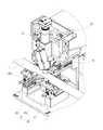
도1은 본 발명의 일실시예에 따른 COF 검사장치의 사시도,
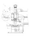
도2는 도1에 표시된 'A'의 확대도,
도3는 본 발명의 일실시예에 따른 COF 검사장치의 측면도,
도4는 본 발명의 일실시예에 따른 촬상부의 부분 단면도,
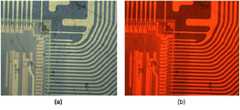
도 5는 본 발명의 일실시예에 따른 촬상부에서 취득한 검사대상칩의 이미지,
도6은 본 발명의 일실시예에 따른 촬상부에서 취득한 검사대상칩 이미지의 부분확대도,
도7은 본 발명의 일실시예에 따른 COF가 일방향으로 이송되는 상태를 도시한 도면,
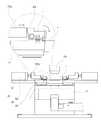
도8a 및 도8b는 본 발명의 일실시예에 따른 클램핑부가 COF 필름을 고정하는 상태를 도시한 도면,
도9는 본 발명의 일실시예에 따른 촬상부가 검사대상칩을 촬상하는 상태를 도시한 도면,1 is a perspective view of a COF inspection apparatus according to an embodiment of the present invention;
Figure 2 is an enlarged view of 'A' shown in Figure 1,
3 is a side view of a COF inspection apparatus according to an embodiment of the present invention;
4 is a partial cross-sectional view of an imaging unit according to an embodiment of the present invention;
5 is an image of an inspection target chip acquired by an imaging unit according to an embodiment of the present invention;
6 is a partially enlarged view of an inspection target chip image acquired by an imaging unit according to an embodiment of the present invention;
7 is a view showing a state in which the COF is transported in one direction according to an embodiment of the present invention;
8A and 8B are views illustrating a state in which a clamping unit fixes a COF film according to an embodiment of the present invention;
9 is a view showing a state in which the imaging unit captures an inspection target chip according to an embodiment of the present invention;
이하에서는 첨부된 도면을 참조하여 본 발명의 바람직한 일 실시예를 상세하게 설명하기로 한다.Hereinafter, a preferred embodiment of the present invention will be described in detail with reference to the accompanying drawings.
도1은 본 발명의 일실시예에 따른 COF 검사장치의 사시도이고, 도2는 도1에 표시된 'A'의 확대도이며, 도3는 본 발명의 일실시예에 따른 COF 검사장치의 측면도이고, 도4는 본 발명의 일실시예에 따른 촬상부의 부분 단면도이다.1 is a perspective view of a COF inspection apparatus according to an embodiment of the present invention, FIG. 2 is an enlarged view of 'A' shown in FIG. 1, and FIG. 3 is a side view of a COF inspection apparatus according to an embodiment of the present invention 4 is a partial cross-sectional view of an imaging unit according to an embodiment of the present invention.
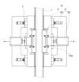
도1 내지 도4에서 보는 바와 같이 본 발명의 일실시예에 따른 칩 온 필름 검사장치는 본체(10)와, 이송부(20)와, 촬상부(30) 및 클램핑부(40)를 포함하여 구성된다.1 to 4, the chip-on-film inspection apparatus according to an embodiment of the present invention includes a
본체(10)는 대략 직육면체의 프레임 형상으로 형성되고, 설치대상영역에 설치되어 후술하는 각 구성의 설치영역을 제공함과 아울러 이들을 지지하는 역할을 한다.The
이송부(20)는 칩 온 필름(이하 'COF'라 함)을 일방향으로 이송하는 역할을 하는 것으로서, 필름 형태의 COF(F)를 일방향으로 이송하기 위해 릴 투 릴 방식이 사용된다. 이에 이송부(20)는 본체(10) 일측에 서로 이격되게 설치된 한 쌍의 릴(21)과, 본체(10)의 타측 중 한 쌍의 릴(21) 사이에 설치되어 COF(F)의 일측을 지지하는 다수의 텐션롤러(22)를 포함하여 구성되며, 한 쌍의 릴(21) 중 COF(F)의 이송방향 후단에 위치한 릴(21)이 회전하면서 COF(F)를 일방향으로 이송한다.The
그리고, 본 실시예는 한 쌍의 릴(21)간 회전속도 또는 텐션롤러(22)를 통한 COF(F)의 장력을 조절하여 COF(F)가 휘어지거나 우그러지는 것을 방지함으로써 이로 인한 검사 오류를 최소화하는 것이 바람직하다.And, this embodiment prevents the COF (F) from being bent or crooked by adjusting the rotation speed between the pair of
촬상부(30)는 본체(10)의 일측 중 COF(F)의 이동경로 상부에 설치되는 라인스캔 카메라(31)와, 라인스캔 카메라(31)와 동축방향으로 조명광을 조사하도록 설치되는 동축조명(32) 및 본체(10)의 일측 중 COF(F) 하부에 설치되는 백라이트(33)를 포함하여 구성되며, COF(F)의 검사대상칩을 촬상하여 검사대상칩에 대한 이미지를 취득하는 역할을 한다.The
라인스캔 카메라(31)는 COF(F)의 폭 방향으로 이동가능하게 설치되고, 검사대상칩의 검사영역에 대응되는 정도의 촬상범위를 갖는 라인스캔 카메라로서, 검사대상칩의 길이방향으로 이동하면서 검사대상칩을 라인스캔하여 검사영역의 이미지를 취득한다.The
본 발명에서는 검사대상칩의 검사영역에 대응되는 길이만큼 촬상소자가 형성되는 라인스캔 카메라(31)가 COF(F)의 폭 방향으로 이동하면서 검사대상칩의 검사영역만을 연속적으로 촬상 즉, COF(F)의 길이방향에 대해 수직방향으로 이동하면서 라인스캔하므로 이미지 취득에 소요되는 시간을 크게 단축시킬 수 있다.In the present invention, the
동축조명(32)은 라인스캔 카메라(31)와 함께 이동하면서 촬상영역에 조명광을 조사하는 역할을 하는데, 라인스캔 카메라(31) 일측에 설치되고 조명광을 조사하는 조명유닛(32a)과, 라인스캔 카메라(31) 일측에 설치되는 하프미러(32b)를 포함하여 구성된다.The
하프미러(32b)는 라인스캔 카메라(31)의 내부 일측 중 렌즈(31a) 축과 동축으로 설치되며, 라인스캔 카메라(31)로부터 조사되는 빛 일부를 통과시키고, 조명유닛(32a)으로부터 조사되는 빛 일부를 촬상영역과 대응되는 영역으로 반사함으로써 검사대상칩 촬상시 촬상영역과 동일한 위치에 조명이 조사될 수 있도록 역할을 한다.The
그리고, 하프미러(32b)는 위에서 설명한 바와 같이 라인스캔 카메라(31) 일측에 설치됨에 따라 라인스캔 카메라(31)가 이동하는 경우 라인스캔 카메라(31)와 함께 이동하여 조명유닛(32a)으로부터 조사되는 빛이 항상 촬상영역으로 조사될 수 있도록 한다.And, the
그리고, 조명유닛(32a)은 라인스캔 카메라(31)의 촬상범위와 대응되는 조명 범위를 갖는 것이 바람직한데, 이는 촬상영역에 광을 집중하여 보다 고품질의 이미지를 취득할 수 있도록 하기 위함이다.In addition, it is preferable that the
또한, 본 발명의 일실시예에 따른 조명유닛(32a)은 적색광을 조사하는 적색 LED인 것이 바람직하다. 적색광의 경우 폴리이미드 재질로 형성된 필름에 대한 투과도가 높아 이미지 내 노이즈 및 콘트라스트가 크게 개선되는 효과가 있었다.In addition, it is preferable that the
백라이트(33)는 본체(10)의 일측 중 COF(F) 하부에 설치되고, 라인스캔 카메라(31)가 이동하는 경우 라인스캔 카메라(31)와 동축을 유지하면서 동반 이동하며, COF(F) 방향으로 광을 조사하여 배경광을 제공하는 역할을 한다.The
여기서, 백라이트(33)는 환경에 따라 다양한 색상의 조명광이 적용될 수 있으나, 본 실시예에서는 백색광이 사용되는 것이 바람직하다.Here, as for the
클램핑부(40)는 본체(10)의 일측 중 COF(F)의 양측부에 각각 COF(F)의 외측방향으로 이동가능하게 설치되는 한 쌍의 이동플레이트(41)와, 한 쌍의 이동플레이트(41) 상면에 각각 설치되는 한 쌍의 지그유닛(42)을 포함하여 구성되며, COF(F)의 양측부를 파지하고 이를 외측방향으로 잡아당겨 COF(F)의 검사영역이 휘어지거나 우그러지는 것을 방지하는 역할을 한다.The clamping
이동플레이트(41)는 대략 플레이트 형상으로 형성되고, 후술하는 한 쌍의 지그유닛(42)에 외측방향으로 이동력을 제공하여 COF(F)의 양측부에 외측방향으로 텐션이 가해지도록 함으로써 COF(F)의 검사영역이 휘어짐이나 우그러짐없이 평찬한 상태를 유지할 수 있도록 하는 역할을 한다.The moving
지그유닛(42)은 본체(10)의 일측 중 COF 양측부에 각각 상하방향으로 회전가능하게 설치되는 고정유닛(42a)과, 본체(10)의 일측 중 고정유닛(42a)의 후단에 전후방향으로 이동가능하게 설치되는 가압부(42b)를 포함하여 구성되며, COF의 양측부를 파지하는 역할을 한다.The
고정유닛(42a)은 길이를 갖는 직육면체의 막대 형상으로 형성되고, COF(F)와 대응되는 일측에는 실리콘 패드가 결합되며, 하방으로 회전하는 경우 COF(F)의 상면 일측을 가압하여 이를 고정하는 역할을 한다.The fixing
그리고, 가압부(42b)는 일반적인 실린더 유닛이 사용될 수 있으며, 실린더 로드(42ba)가 신장하는 경우 고정유닛(42a)의 후단부를 가압함으로써 고정유닛(42a)이 하방으로 이동되도록 하는 역할을 한다.In addition, a general cylinder unit may be used as the
한편, 본 실시예는 본체(10)와 고정유닛(42a) 사이에 스프링과 같은 탄성부재(K)가 설치되어 가압부(42b)의 가압력이 해제되는 경우 탄성부재(K)의 탄성력에 의해 고정유닛(42a)이 초기위치로 복귀할 수 있다.On the other hand, in this embodiment, when an elastic member (K) such as a spring is installed between the
도5는 본 발명의 일실시예에 따른 촬상부에서 취득한 검사대상칩의 이미지이고, 도6은 본 발명의 일실시예에 따른 촬상부에서 취득한 검사대상칩 이미지의 부분확대도이다.5 is an image of the inspection target chip acquired by the imaging unit according to an embodiment of the present invention, and FIG. 6 is a partially enlarged view of the inspection target chip image acquired by the imaging unit according to the embodiment of the present invention.
도5는 본 실시예에 따른 COF 검사장치(1)에서 일반적인 동축조명으로 사용되는 백색광과 적색광 조명을 이용하여 취득한 이미지를 나타낸 것으로서, (a)는 백색 조명광, (b)는 적색조명광을 이용하여 취득한 이미지이다.5 shows images obtained using white light and red light illumination used as general coaxial illumination in the
COF의 본딩 검사를 위해서는 칩이 하부를 향하도록 배치된 상태에서 검사가 이루어지는데, 조명광이 필름을 투과한 후 검사영역에서 반사되어 카메라로 입사된다. 그런데, 도 5의 (a) 이미지를 살펴보면 백색 조명광을 이용하여 취득한 이미지는 폴리이미드 재질의 필름 표면으로 인한 노이즈 성분이 많아 검사 오류 발생 가능성이 높은데 반해, 적색 조명광을 이용하여 취득한 이미지는 폴리이미드 재질의 필름 표면으로 인한 노이즈 성분이 상대적으로 훨씬 적은 것을 알 수 있으며, 적색광의 특성상 높은 콘트라스트를 갖는 영상을 얻을 수 있어 검사 정확도가 보다 향상된다.For the COF bonding inspection, the inspection is performed with the chip facing downward. After the illumination light passes through the film, it is reflected from the inspection area and is incident on the camera. However, looking at the image (a) of FIG. 5, the image acquired using the white illumination light has a high probability of inspection errors due to the high noise component due to the film surface of the polyimide material, whereas the image acquired using the red illumination light is a polyimide material It can be seen that the noise component due to the surface of the film is relatively much less, and the image with high contrast can be obtained due to the characteristic of red light, and the inspection accuracy is further improved.
한편, 도 6은 백라이트 조명을 이용하여 검사대상 칩의 포팅영역(Potting Area, 칩의 수지 충진 영역)을 촬영한 이미지로서 포팅영역의 파티클 존재 여부를 검사하기 위해 사용된다. (a) 이미지는 일반적인 비전 카메라에 사용되는 낮은 개구수를 갖는 대물렌즈를 이용하여 포팅영역을 촬영한 경우에 취득한 이미지로서 적색 점선으로 둘러싸인 영역이 포팅영역이다. (a) 이미지에서 포팅영역을 살펴보면 포팅영역 내부에 청색 점선으로 표시된 라인 형상의 노이즈가 발생함을 알 수 있다. 이러한 라인형상의 노이즈는 해당 부분에 존재하는 파티클 검사 오류의 주된 원인이 된다.Meanwhile, FIG. 6 is an image obtained by photographing a potting area (resin filling area of a chip) of a chip to be inspected using backlight illumination, and is used to examine whether or not particles exist in the potting area. (a) The image is an image obtained when the potting area is photographed using an objective lens having a low numerical aperture used in a general vision camera, and the area surrounded by the red dotted line is the potting area. (a) Looking at the potting area in the image, it can be seen that the line-shaped noise indicated by the blue dotted line is generated inside the potting area. Such line-shaped noise is the main cause of particle inspection errors existing in the corresponding part.
본 출원인은 이러한 라인 노이즈 발생원인을 면밀하게 연구한 결과 그 원인이 낮은 개구수를 갖는 렌즈를 사용하는 경우 빛의 굴절각에 의해 포팅영역 외곽에 라인 형상 노이즈가 발생하는 것을 알게 되었고, 오랜 연구결과 0.02 내지 0.05의 높은 개구수(N/A)의 렌즈를 사용하는 경우 포팅영역에서 선 형태의 노이즈가 발생하지 않음을 확인할 수 있었다.As a result of in-depth research on the causes of line noise, the present applicant found that when a lens with a low numerical aperture is used, line-shaped noise occurs outside the potting area due to the refraction angle of light. It was confirmed that, when a lens having a high numerical aperture (N/A) of 0.05 to 0.05 was used, no linear noise was generated in the potting area.
이처럼 본 출원인은 적색조명과 높은 개구수를 갖는 렌즈를 사용함으로써 노이즈가 적으면서도 해상도가 높은 고품질의 이미지를 취득하여 검사의 신뢰도를 크게 향상시킬 수 있는 검사장치를 개발할 수 있게 되었다.As such, the present applicant has been able to develop an inspection apparatus capable of greatly improving the reliability of inspection by acquiring high-quality images with low noise and high resolution by using red illumination and a lens having a high numerical aperture.
도7은 본 발명의 일실시예에 따른 COF가 일방향으로 이송되는 상태를 도시한 도면이고, 도8a 및 도8b는 본 발명의 일실시예에 따른 클램핑부가 COF 필름을 고정하는 상태를 도시한 도면이며, 도9는 본 발명의 일실시예에 따른 촬상부가 검사대상칩을 촬상하는 상태를 도시한 도면으로서, 본 발명에 따른 칩 온 필름 검사장치의 동작을 도7 내지 도9를 참조하여 설명하면 다음과 같다.7 is a view showing a state in which the COF is transported in one direction according to an embodiment of the present invention, and FIGS. 8A and 8B are views showing a state in which the clamping unit secures the COF film according to an embodiment of the present invention; 9 is a view showing a state in which the imaging unit captures an inspection target chip according to an embodiment of the present invention. The operation of the chip-on-film inspection apparatus according to the present invention will be described with reference to FIGS. 7 to 9. As follows.
먼저, COF(F)의 양측단부가 각각 한 쌍의 릴(21)에 연결되며, COF(F)의 일측에 텐션롤러(22)에 지지되어 장력이 설정된다. 그리고, 한 쌍의 릴(21) 중 어느 하나의 릴(21)이 회전하고, 이에 다른 하나의 릴(21)이 동반하여 자유회전함으로써 COF(F)가 일방향으로 이동되며, COF(F)에 실장된 검사대상칩(C)이 촬상부(30)와 대응되는 위치에 배치된다.First, both ends of the COF (F) are connected to a pair of
검사대상칩(C)이 촬상부(30)와 대응되는 위치에 배치되면, 가압부(42b)가 전진하여 고정유닛(42a)의 후단부를 가압하고, COF(F) 양측부에 배치된 고정유닛(42a)이 하방으로 회전하여 COF(F)의 양측부를 고정파지한다. 그리고, 이동플레이트(41)가 외측방향으로 이동하여 고정유닛(42)이 COF(F)의 양측부를 외측방향으로 당김으로써 검사대상칩(C)이 실장된 COF(F)의 검사영역이 평탄화되도록 한다.When the inspection target chip (C) is disposed at a position corresponding to the
라인스캔 카메라(31)는 검사대상칩(C)의 길이방향과 대응되는 방향으로 이동함과 동시에 검사대상칩(C)을 촬상하는데, 동축조명(32)에서 조사된 적색광이 하프미러(32b)에 의해 반사되어 촬상영역에 조사된다. 동시에 백라이트(33)가 라인스캔 카메라(31)와 동축을 유지하면서 동반 이동한다.The
즉, 본 실시예에 따른 COF 검사장치(1)는 라인스캔 카메라(31)가 검사대상칩(C)을 촬상하는 경우 동축조명(32)과, 백라이트(33)가 라인스캔 카메라(31)와 동축 상에서 동반 이동하므로 촬상영역에 조사되는 조명광과 백라이트 광이 일정하게 유지되어 항상 균일한 품질의 이미지를 취득할 수 있다.That is, in the
비록 본 발명이 상기 언급된 바람직한 실시예와 관련하여 설명되어졌지만, 발명의 요지와 범위로부터 벗어남이 없이 다양한 수정이나 변형을 하는 것이 가능하다. 따라서 첨부된 특허청구의 범위는 본 발명의 요지에서 속하는 이러한 수정이나 변형을 포함할 것이다.Although the present invention has been described with reference to the above-mentioned preferred embodiments, various modifications and variations are possible without departing from the spirit and scope of the invention. Accordingly, the appended claims are intended to cover such modifications and variations as fall within the scope of the present invention.
10 : 본체20 : 이송부
21 : 릴22 : 텐션롤러
30 : 촬상부31 : 라인스캔 카메라
31a : 렌즈32 : 동축조명
32a : 조명유닛32b : 하프미러
33 : 백라이트40 : 클램핑부
41 : 이동플레이트42 : 지그유닛
42a : 고정유닛42b : 가압부
42ba : 실린더 로드10: body 20: transfer unit
21: reel 22: tension roller
30: imaging unit 31: line scan camera
31a: lens 32: coaxial illumination
32a:
33: backlight 40: clamping part
41: moving plate 42: jig unit
42a: fixed
42ba : cylinder rod
Claims (5)
Translated fromKorean상기 본체의 일측에 설치되고, 폴리이미드 재질의 필름 저면에 검사대상칩이 실장된 칩 온 필름(COF)을 일방향으로 이송하는 이송부와;
상기 칩 온 필름의 이동로 일측 상부에 설치되고, 상기 검사대상칩을 촬상하여 이미지를 취득하는 촬상부; 및
상기 칩 온 필름의 이동로 일측 중 상기 촬상부 하부에 설치되고, 상기 칩 온 필름의 일측을 고정 및 고정해제하는 클램핑부를 포함하되,
상기 촬상부는
상기 클램핑부의 상부에 상기 검사대상칩의 길이방향으로 이동가능하게 설치되고 상기 검사대상칩의 길이방향으로 이동함과 동시에 상기 검사대상칩을 촬상하며 렌즈의 개구수가 0.02 내지 0.05인 라인스캔 카메라와, 상기 본체의 일측에 설치되고, 상기 라인스캔 카메라의 촬상영역과 대응되는 조명영역을 가지며, 적색광을 조사하는 동축조명 및 상기 본체의 일측 중 상기 칩 온 필름 하부에 상기 검사대상칩의 길이방향으로 이동가능하게 설치되고 일측이 상기 촬상부의 일측에 일체로 결합되어 상기 라인스캔 카메라가 이동하는 경우 상기 라인스캔 카메라와 동축을 유지하면서 이동하는 백라이트를 포함하며,
상기 클램핑부는 상기 본체의 일측 중 상기 칩 온 필름의 양측부에 각각 상기 칩 온 필름의 측부 외측방향으로 이동가능하게 설치되는 한 쌍의 이동플레이트와, 상기 한 쌍의 이동플레이트에 각각 회전가능하게 설치되고 하방으로 회전하는 경우 상기 칩 온 필름의 양측부를 가압고정하는 한 쌍의 지그유닛을 포함하고,
상기 지그유닛은 상기 본체의 일측 중 상기 칩 온 필름 양측부에 각각 상하방향으로 회전가능하게 설치되고 하방으로 회전하는 경우 상기 칩 온 필름의 상면 일측을 가압지지하는 고정유닛과, 상기 본체와 상기 고정유닛 사이에 설치되고 상기 고정유닛에 상방으로 탄성력을 제공하는 탄성부재 및 상기 본체의 일측 중 상기 고정유닛의 후단에 전후방향으로 이동가능하게 설치되고 전방으로 이동하는 경우 상기 고정유닛의 후단을 가압하여 상기 고정유닛이 하방으로 회전되도록 하는 가압부를 포함하는 것을 특징으로 하는 칩 온 필름 검사장치.
a body;
a transfer unit installed on one side of the main body and unidirectionally transferring a chip-on-film (COF) on which a chip to be inspected is mounted on a bottom surface of a polyimide film;
an imaging unit installed on one side of the moving path of the chip-on-film and acquiring an image by imaging the test target chip; and
A clamping unit installed under the imaging unit on one side of the moving path of the chip-on-film and fixing and releasing one side of the chip-on-film;
The imaging unit
a line scan camera installed movably in the longitudinal direction of the chip to be inspected on the clamping part and moving in the longitudinal direction of the chip to be inspected while imaging the chip to be inspected and having a numerical aperture of 0.02 to 0.05; Installed on one side of the main body, having an illumination area corresponding to the imaging area of the line scan camera, coaxial illumination irradiating red light and moving in the longitudinal direction of the chip to be inspected under the chip-on-film among one side of the main body and a backlight installed so as to be possible and one side integrally coupled to one side of the imaging unit to move while maintaining coaxiality with the linescan camera when the linescan camera moves,
The clamping part includes a pair of movable plates movably installed on both sides of the chip-on-film among one side of the main body in an outward direction of the side of the chip-on-film, respectively, and rotatably installed on the pair of movable plates, respectively and a pair of jig units for pressing and fixing both sides of the chip on film when rotating downward,
The jig unit includes a fixing unit rotatably installed on both sides of the chip-on-film on one side of the main body, respectively, and pressurizing and supporting one side of the upper surface of the chip-on-film when rotating downward, and the main body and the fixing unit An elastic member installed between the units and providing an upward elastic force to the fixing unit and a rear end of the fixing unit among one side of the main body is movably installed in the front-rear direction and when moving forward, pressing the rear end of the fixing unit Chip-on-film inspection device, characterized in that it comprises a pressing unit for rotating the fixing unit downward.
상기 동축조명은
상기 라인스캔 카메라 일측에 설치되고 적색광을 조사하는 조명유닛과;
상기 라인스캔 카메라 일측에 설치되되, 상기 라인스캔 카메라의 렌즈와 동축에 설치되고, 상기 동축조명으로부터 조사된 빛 일부를 상기 촬상영역과 대응되는 영역으로 반사하는 하프미러를 포함하는 것을 특징으로 하는 칩 온 필름 검사장치.
According to claim 1,
The coaxial lighting is
a lighting unit installed on one side of the line scan camera and irradiating red light;
A chip installed on one side of the linescan camera, installed on the same axis as the lens of the linescan camera, and comprising a half-mirror that reflects a portion of the light irradiated from the coaxial illumination to an area corresponding to the imaging area On-film inspection device.
Priority Applications (1)
| Application Number | Priority Date | Filing Date | Title |
|---|---|---|---|
| KR1020200119667AKR102267705B1 (en) | 2020-09-17 | 2020-09-17 | Inspection apparatus for chip on film |
Applications Claiming Priority (1)
| Application Number | Priority Date | Filing Date | Title |
|---|---|---|---|
| KR1020200119667AKR102267705B1 (en) | 2020-09-17 | 2020-09-17 | Inspection apparatus for chip on film |
Publications (1)
| Publication Number | Publication Date |
|---|---|
| KR102267705B1true KR102267705B1 (en) | 2021-06-22 |
Family
ID=76600355
Family Applications (1)
| Application Number | Title | Priority Date | Filing Date |
|---|---|---|---|
| KR1020200119667AActiveKR102267705B1 (en) | 2020-09-17 | 2020-09-17 | Inspection apparatus for chip on film |
Country Status (1)
| Country | Link |
|---|---|
| KR (1) | KR102267705B1 (en) |
Citations (6)
| Publication number | Priority date | Publication date | Assignee | Title |
|---|---|---|---|---|
| KR100772608B1 (en)* | 2006-05-29 | 2007-11-02 | 아주하이텍(주) | Auto optical inspection system |
| KR101183179B1 (en) | 2010-04-22 | 2012-09-14 | (주)에이앤아이 | Method for checking of cof appearance using laser 3d measuring machine |
| JP5056339B2 (en)* | 2007-10-18 | 2012-10-24 | 凸版印刷株式会社 | Substrate gripping mechanism for substrate transfer equipment |
| KR101577119B1 (en)* | 2013-02-15 | 2015-12-11 | 가부시키가이샤 스크린 홀딩스 | Pattern inspection apparatus and pattern inspection method |
| KR20160004099A (en)* | 2014-07-02 | 2016-01-12 | 한화테크윈 주식회사 | Defect inspecting apparatus |
| KR102071357B1 (en)* | 2019-02-20 | 2020-01-30 | 주식회사 이엔씨 테크놀로지 | Inspection equipment for inspecting flexible display device and stage apparatus used therein |
- 2020
- 2020-09-17KRKR1020200119667Apatent/KR102267705B1/enactiveActive
Patent Citations (6)
| Publication number | Priority date | Publication date | Assignee | Title |
|---|---|---|---|---|
| KR100772608B1 (en)* | 2006-05-29 | 2007-11-02 | 아주하이텍(주) | Auto optical inspection system |
| JP5056339B2 (en)* | 2007-10-18 | 2012-10-24 | 凸版印刷株式会社 | Substrate gripping mechanism for substrate transfer equipment |
| KR101183179B1 (en) | 2010-04-22 | 2012-09-14 | (주)에이앤아이 | Method for checking of cof appearance using laser 3d measuring machine |
| KR101577119B1 (en)* | 2013-02-15 | 2015-12-11 | 가부시키가이샤 스크린 홀딩스 | Pattern inspection apparatus and pattern inspection method |
| KR20160004099A (en)* | 2014-07-02 | 2016-01-12 | 한화테크윈 주식회사 | Defect inspecting apparatus |
| KR102071357B1 (en)* | 2019-02-20 | 2020-01-30 | 주식회사 이엔씨 테크놀로지 | Inspection equipment for inspecting flexible display device and stage apparatus used therein |
Similar Documents
| Publication | Publication Date | Title |
|---|---|---|
| JP5127301B2 (en) | Automatic optical inspection apparatus, automatic optical inspection system, and automatic optical inspection method | |
| JP5038191B2 (en) | Electronic component inspection method and apparatus used therefor | |
| KR100969283B1 (en) | Optical inspection device | |
| US20050162517A1 (en) | Method and apparatus for testing image pickup device | |
| CN100402974C (en) | Check device | |
| JP6176789B2 (en) | Electronic component inspection equipment | |
| CN111678921B (en) | Optical inspection equipment | |
| TWI816353B (en) | Optical testing system | |
| KR102267705B1 (en) | Inspection apparatus for chip on film | |
| KR100933467B1 (en) | AOI device | |
| KR20130035827A (en) | Apparatus for automated optical inspection | |
| KR20220059781A (en) | Inspection apparatus for chip on film | |
| KR20080088946A (en) | Three-dimensional shape inspection device and three-dimensional shape inspection method using the same | |
| KR20070119868A (en) | Reel unit optical inspection device and method | |
| JP2006292412A (en) | Surface inspection system, surface inspection method and substrate manufacturing method | |
| KR102242093B1 (en) | An apparatus for inspecting metal mask | |
| KR100417764B1 (en) | An apparatus and a method for defect inspection | |
| KR20040107440A (en) | Apparatus and method for inspecting film carrier tape for mounting electronic component | |
| KR20110117371A (en) | Pattern checker | |
| KR20080089314A (en) | Three-dimensional shape inspection device and three-dimensional shape inspection method using the same | |
| JP2001083098A (en) | Optical surface inspection mechanism and device | |
| JP2862833B2 (en) | Solder appearance inspection device | |
| KR102323583B1 (en) | Line scan inspection device | |
| CN223051216U (en) | A high-precision appearance inspection device and equipment based on printed circuits | |
| KR102421125B1 (en) | Lighting module of surface defect inspection apparatus |
Legal Events
| Date | Code | Title | Description |
|---|---|---|---|
| PA0109 | Patent application | Patent event code:PA01091R01D Comment text:Patent Application Patent event date:20200917 | |
| PA0201 | Request for examination | ||
| PA0302 | Request for accelerated examination | Patent event date:20200917 Patent event code:PA03022R01D Comment text:Request for Accelerated Examination | |
| PE0902 | Notice of grounds for rejection | Comment text:Notification of reason for refusal Patent event date:20201030 Patent event code:PE09021S01D | |
| PE0701 | Decision of registration | Patent event code:PE07011S01D Comment text:Decision to Grant Registration Patent event date:20210421 | |
| GRNT | Written decision to grant | ||
| PR0701 | Registration of establishment | Comment text:Registration of Establishment Patent event date:20210616 Patent event code:PR07011E01D | |
| PR1002 | Payment of registration fee | Payment date:20210616 End annual number:3 Start annual number:1 | |
| PG1601 | Publication of registration |