KR102266069B1 - Wireline transceiver based on pulse amplitude modulation-4 - Google Patents
Wireline transceiver based on pulse amplitude modulation-4Download PDFInfo
- Publication number
- KR102266069B1 KR102266069B1KR1020200084682AKR20200084682AKR102266069B1KR 102266069 B1KR102266069 B1KR 102266069B1KR 1020200084682 AKR1020200084682 AKR 1020200084682AKR 20200084682 AKR20200084682 AKR 20200084682AKR 102266069 B1KR102266069 B1KR 102266069B1
- Authority
- KR
- South Korea
- Prior art keywords
- modulated signal
- pam
- signal
- current source
- modulated
- Prior art date
- Legal status (The legal status is an assumption and is not a legal conclusion. Google has not performed a legal analysis and makes no representation as to the accuracy of the status listed.)
- Active
Links
Images


Classifications
- H—ELECTRICITY
- H04—ELECTRIC COMMUNICATION TECHNIQUE
- H04L—TRANSMISSION OF DIGITAL INFORMATION, e.g. TELEGRAPHIC COMMUNICATION
- H04L25/00—Baseband systems
- H04L25/02—Details ; arrangements for supplying electrical power along data transmission lines
- H04L25/026—Arrangements for coupling transmitters, receivers or transceivers to transmission lines; Line drivers
- H—ELECTRICITY
- H04—ELECTRIC COMMUNICATION TECHNIQUE
- H04L—TRANSMISSION OF DIGITAL INFORMATION, e.g. TELEGRAPHIC COMMUNICATION
- H04L25/00—Baseband systems
- H04L25/02—Details ; arrangements for supplying electrical power along data transmission lines
- H04L25/0264—Arrangements for coupling to transmission lines
- H04L25/028—Arrangements specific to the transmitter end
- H—ELECTRICITY
- H04—ELECTRIC COMMUNICATION TECHNIQUE
- H04L—TRANSMISSION OF DIGITAL INFORMATION, e.g. TELEGRAPHIC COMMUNICATION
- H04L25/00—Baseband systems
- H04L25/02—Details ; arrangements for supplying electrical power along data transmission lines
- H04L25/0264—Arrangements for coupling to transmission lines
- H04L25/0292—Arrangements specific to the receiver end
- H—ELECTRICITY
- H04—ELECTRIC COMMUNICATION TECHNIQUE
- H04L—TRANSMISSION OF DIGITAL INFORMATION, e.g. TELEGRAPHIC COMMUNICATION
- H04L25/00—Baseband systems
- H04L25/02—Details ; arrangements for supplying electrical power along data transmission lines
- H04L25/03—Shaping networks in transmitter or receiver, e.g. adaptive shaping networks
- H04L25/03006—Arrangements for removing intersymbol interference
- H—ELECTRICITY
- H04—ELECTRIC COMMUNICATION TECHNIQUE
- H04L—TRANSMISSION OF DIGITAL INFORMATION, e.g. TELEGRAPHIC COMMUNICATION
- H04L25/00—Baseband systems
- H04L25/38—Synchronous or start-stop systems, e.g. for Baudot code
- H04L25/40—Transmitting circuits; Receiving circuits
- H04L25/49—Transmitting circuits; Receiving circuits using code conversion at the transmitter; using predistortion; using insertion of idle bits for obtaining a desired frequency spectrum; using three or more amplitude levels ; Baseband coding techniques specific to data transmission systems
Landscapes
- Engineering & Computer Science (AREA)
- Computer Networks & Wireless Communication (AREA)
- Signal Processing (AREA)
- Power Engineering (AREA)
- Physics & Mathematics (AREA)
- Spectroscopy & Molecular Physics (AREA)
- Dc Digital Transmission (AREA)
Abstract
Translated fromKoreanDescription
Translated fromKorean본 출원은 PAM-4 기반의 유선 트랜시버에 관한 것으로, 특히, 4개의 비트를 4개의 와이어를 통해 송수신하는 4레벨-펄스진폭변조 신호법을 적용한 유선 트랜시버에 관한 것이다.This application relates to a wired transceiver based on PAM-4, and more particularly, to a wired transceiver to which a 4-level-pulse amplitude modulation signal method for transmitting and receiving 4 bits through 4 wires is applied.
데이터 통신을 위해서 일반적으로 NRZ(PAM-2) 신호법을 사용한다. 여기서, NRZ(PAM-2) 신호법은 두 가지 데이터 변조 레벨을 가지며, 송수신기의 구조를 간단하게 할 수 있다.For data communication, the NRZ (PAM-2) signaling method is generally used. Here, the NRZ (PAM-2) signaling method has two data modulation levels, and the structure of the transceiver can be simplified.
그러나, NRZ(PAM-2) 신호법은 1 unit interval(UI) 동안 1bit 데이터만 전송 할 수 있기 때문에, 클락 주파수를 높이는 것으로는 한계가 있고, 고속 데이터 전송 시 채널의 영향을 많이 받아 고속 송수신기 구현에 어려운 문제를 가진다.However, since the NRZ (PAM-2) signaling method can transmit only 1 bit data for 1 unit interval (UI), there is a limit to increasing the clock frequency, and it is greatly affected by the channel during high-speed data transmission, so a high-speed transceiver is implemented. have a difficult problem with
최근, NRZ(PAM-2) 신호법의 단점을 보완하기 위해, 네 개의 데이터 변조 레벨을 가지고 1UI에 2bit를 보낼 수 있는 PAM-4 신호법이 사용되고 있다.Recently, in order to compensate for the shortcomings of the NRZ (PAM-2) signaling method, the PAM-4 signaling method capable of transmitting 2 bits in 1 UI with four data modulation levels is used.
이러한 PAM-4 신호법은 NRZ(PAM-2) 신호법에 비해 데이터 변조 레벨 간의 간격이 1/3배로 작기 때문에, 데이터 변조 레벨 간의 간격이 일정하지 않을 때, 가장 작은 간격으로 인하여 신호대잡음 비율이 떨어지고, 전압 마진이 낮은 문제를 가진다.In this PAM-4 signal method, the interval between data modulation levels is 1/3 times smaller than that of the NRZ (PAM-2) signal method. Therefore, when the interval between data modulation levels is not constant, the signal-to-noise ratio is reduced due to the smallest interval. drop, and the voltage margin is low.
본 출원의 목적은 개의 레벨 펄스 진폭 변조 신호 법을 적용한 PAM-4 기반의 유선 트랜시버를 제공하기 위한 것이다.It is an object of the present application to provide a wired transceiver based on PAM-4 to which a signal method of n level pulse amplitude modulation is applied.
본 출원의 일 실시예에 따른 PAM-4 기반의 유선 트랜시버는 변조 신호를 송신하는 송신부 및 상기 변조 신호로부터 기설정된 디코딩 테이블을 통해 결정되는 복수의 결정 값들에 기초하여, 디지털 출력 신호를 생성하는 수신부를 포함하고, 상기 송신부와 상기 수신부는 상기 복수의 와이어들을 통해 서로 연결된다.A PAM-4 based wired transceiver according to an embodiment of the present application includes a transmitter for transmitting a modulated signal and a receiver for generating a digital output signal based on a plurality of decision values determined from the modulated signal through a predetermined decoding table Including, the transmitter and the receiver are connected to each other through the plurality of wires.
본 출원의 다른 실시예에 따른 PAM-4 기반의 유선 트랜시버는 송신 신호에 따라 인코딩된 변조 신호의 각 출력 전압을 조절하는 송신부 및 상기 변조 신호의 각 출력 전압에 기초하여, 상기 변조 신호로부터 결정되는 복수의 결정 값들 중 적어도 일부를 디지털 출력 신호로 디코딩하는 수신부를 포함하고, 상기 송신부는 상기 변조 신호의 각 출력 전압을 복수의 와이어들을 통해 상기 수신부로 출력한다.A PAM-4 based wired transceiver according to another embodiment of the present application is a transmitter that adjusts each output voltage of a modulated signal encoded according to a transmit signal, and based on each output voltage of the modulated signal, determined from the modulated signal and a receiving unit that decodes at least a portion of the plurality of determination values into a digital output signal, wherein the transmitting unit outputs each output voltage of the modulated signal to the receiving unit through a plurality of wires.
본 출원의 실시예에 따른 PAM-4 기반의 유선 트랜시버는 고속의 송수신 속도를 제공하는 동시에, 종래의 싱글단 타입의 NRZ 트랜시버 및 기존 차동 PAM-4 트랜시버와 같은 핀 효율성을 가지며, 종래의 PAM-4 신호법에 비해 2배의 높은 전압 마진을 확보하여 신호대잡음 비율을 증가시킬 수 있고, 채널 감쇄로 인해 발생할 수 있는 부호 간 간섭을 제거할 수 있다.The PAM-4 based wired transceiver according to the embodiment of the present application provides high transmission/reception speed and at the same time has the same pin efficiency as the conventional single-stage type NRZ transceiver and the existing differential PAM-4 transceiver, and the conventional PAM- It is possible to increase the signal-to-noise ratio by securing a voltage margin that is twice as high as that of the 4-signal method, and to eliminate inter-symbol interference that may occur due to channel attenuation.
도 1은 본 출원의 일 실시예에 따른 PAM-4 기반의 유선 트랜시버에 대한 블록도이다.
도 2는 도 1의 변조 신호에 대한 실시 예를 나타내는 도이다.
도 3은 도 1의 수신부에 기설정된 디코딩 테이블을 설명하기 위한 도이다.
도 4는 도 1의 수신부에 대한 블록도이다.
도 5는 도 4의 수신부를 구체적으로 보여주는 도이다.
도 6은 도 5의 아날로그 전단부를 구체적으로 나타내는 도이다.
도 7은 도 5의 판정 궤환 등화부를 구체적으로 나타내는 도이다.
도 8은 도 5의 디코딩부를 구체적으로 나타내는 도이다.
도 9는 본 출원의 다른 실시예에 따른 PAM-4 기반의 유선 트랜시버에 대한 블록도이다.
도 10은 도 9의 송신부를 구체적으로 보여주는 도이다
도 11은 도 10의 인코딩부에 기설정된 인코딩 맵핑 테이블을 설명하기 위한 도이다.
도 12는 도 10의 드라이버부에 기설정된 인코딩 로직 테이블을 설명하기 위한 도이다.
도 13은 도 10의 드라이버부를 구체적으로 보여주는 도이다.
도 14는 도 13의 드라이버부의 동작 예이다.1 is a block diagram of a PAM-4 based wired transceiver according to an embodiment of the present application.
FIG. 2 is a diagram illustrating an embodiment of the modulated signal of FIG. 1 .
FIG. 3 is a diagram for explaining a decoding table preset in the receiver of FIG. 1 .
FIG. 4 is a block diagram of the receiver of FIG. 1 .
FIG. 5 is a diagram specifically illustrating the receiver of FIG. 4 .
6 is a diagram specifically illustrating an analog front end of FIG. 5 .
FIG. 7 is a diagram specifically illustrating a decision feedback equalizer of FIG. 5 .
8 is a diagram specifically illustrating the decoding unit of FIG. 5 .
9 is a block diagram of a PAM-4 based wired transceiver according to another embodiment of the present application.
FIG. 10 is a diagram specifically showing the transmitter of FIG. 9 .
11 is a diagram for explaining an encoding mapping table preset in the encoding unit of FIG. 10 .
12 is a diagram for explaining an encoding logic table preset in the driver unit of FIG. 10 .
13 is a diagram specifically illustrating the driver unit of FIG. 10 .
14 is an operation example of the driver unit of FIG. 13 .
이하, 구체적인 실시형태 및 첨부된 도면을 참조하여 본 출원의 실시형태를 설명한다. 그러나, 본 출원의 실시 형태는 여러 가지 다른 형태로 변형될 수 있으며, 본 출원의 범위가 이하 설명하는 실시형태로 한정되는 것은 아니다. 또한, 본 출원의 실시형태는 통상의 기술자에게 본 발명을 더욱 완전하게 설명하기 위해서 제공되는 것이다. 따라서, 도면에서의 요소들의 형상 및 크기 등은 보다 명확한 설명을 위해 과장될 수 있으며, 도면상의 동일한 부호로 표시되는 요소는 동일한 요소이다.DETAILED DESCRIPTION OF THE PREFERRED EMBODIMENTS Hereinafter, embodiments of the present application will be described with reference to specific embodiments and the accompanying drawings. However, the embodiments of the present application may be modified in various other forms, and the scope of the present application is not limited to the embodiments described below. In addition, the embodiments of the present application are provided in order to more completely explain the present invention to those skilled in the art. Accordingly, the shapes and sizes of elements in the drawings may be exaggerated for clearer description, and elements indicated by the same reference numerals in the drawings are the same elements.
그리고 도면에서 본 출원을 명확하게 설명하기 위해서 설명과 관계없는 부분은 생략하고, 여러 층 및 영역을 명확하게 표현하기 위하여 두께를 확대하여 나타내었으며, 동일한 사상의 범위 내의 기능이 동일한 구성요소는 동일한 참조부호를 사용하여 설명한다. 나아가, 명세서 전체에서, 어떤 부분이 어떤 구성요소를 "포함"한다고 할때, 이는 특별히 반대되는 기재가 없는 한 다른 구성요소를 제외하는 것이 아니라 다른 구성요소를 더 포함할 수 있는 것을 의미한다.And in order to clearly explain the present application in the drawings, parts irrelevant to the description are omitted, and the thickness is enlarged to clearly express various layers and regions, and components having the same function within the scope of the same idea are referred to as the same. It is explained using symbols. Furthermore, throughout the specification, when a part "includes" a certain element, it means that other elements may be further included, rather than excluding other elements, unless otherwise stated.
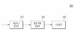
도 1은 본 출원의 일 실시예에 따른 PAM-4 기반의 유선 트랜시버(10)에 대한 블록도이고, 도 2는 도 1의 변조 신호(AMBMCMDM)에 대한 실시 예를 나타내는 도이고, 도 3은 도 1의 수신부(200)에 기설정된 디코딩 테이블(300)을 나타내는 도이다.1 is a block diagram of a PAM-4 based
도 1을 참조하면, PAM-4 기반의 유선 트랜시버(10)는 송신부(100)와 수신부(200)를 포함할 수 있다.Referring to FIG. 1 , a PAM-4 based
먼저, 송신부(100)는 변조 신호(AMBMCMDM)를 복수의 와이어들(W1~W4)을 통해 송신할 수 있다. 여기서, 복수의 와이어들(W1~W4)은 송신부(100)와 수신부(200)를 서로 연결하는 배선일 수 있다.First, the
실시예에 따른 변조 신호(AMBMCMDM)는 단위 시간(1 Unit Interval, 1 UI)마다 서로 다른 전압 레벨을 가지는 제1 내지 제4 변조 비트를 포함할 수 있다.The modulation signal A M BM CM DM according to the embodiment may include first to fourth modulation bits having different voltage levels for each unit time (1 Unit Interval, 1 UI).
예를 들면, 도 2에 도시된 바와 같이, 1 UI 구간에서, 제1 변조 비트는 하이 전압 레벨이고, 제2 변조 비트는 하이 전압 레벨보다 작은 제1 중간 전압 레벨이며, 제3 변조 비트는 제1 중간 전압 레벨보다 작은 제2 중간 전압 레벨이고, 제4 변조 비트는 제2 중간 전압 레벨보다 작은 로우 전압 레벨일 수 있다.For example, as shown in FIG. 2 , in 1 UI section, the first modulation bit is a high voltage level, the second modulation bit is a first intermediate voltage level smaller than the high voltage level, and the third modulation bit is the second modulation bit. The second intermediate voltage level may be less than the first intermediate voltage level, and the fourth modulation bit may be a low voltage level less than the second intermediate voltage level.
여기서, 제1 내지 제4 변조 비트는 복수의 와이어들(W1~W4)에 일대일 대응될 수 있다. 예를 들면, 제1 변조 비트는 복수의 와이어들(W1~W4) 중 제1 와이어(W1)를 통해 송신되고, 제2 변조 비트는 복수의 와이어들(W1~W4) 중 제1 와이어(W2)를 통해 송신될 수 있다.Here, the first to fourth modulation bits may correspond one-to-one to theplurality of wires W 1 to W4 . For example, the first modulated bit is a plurality of wires (W1 ~ W4) of
본 출원의 실시예에 따른 수신부(200)는 변조 신호(AMBMCMDM)로부터 기설정된 디코딩 테이블을 통해 결정되는 복수의 결정 값들(A-B, A-C, A-D, B-C, B-D, C-D) 중 적어도 일부(A-B, A-D, B-C, C-D)에 기초하여, 디지털 출력 신호(ABCD)를 생성함으로써, 기존 싱글단 타입의 NRZ 트랜시버 및 기존 차동 PAM-4 트랜시버와 같은 핀 효율성을 가지며, 기존 PAM-4 신호법에 비해 2배의 높은 전압 마진을 확보하며, 채널 감쇄로 인해 발생할 수 있는 부호 간 간섭을 제거할 수 있다.The
여기서, 디지털 출력 신호(ABCD)는 단위 시간(1UI)마다 4 비트의 정보를 가진 신호일 수 있다.Here, the digital output signal ABCD may be a signal having 4 bits of information per unit time (1UI).
이때, 기설정된 디코딩 테이블(300)은 도 3에 도시된 바와 같이, 변조 신호(AMBMCMDM)에 대한 경우의 수가 맵핑된 변조 비트 테이블(310), 복수의 결정 값들(A-B, A-C, A-D, B-C, B-D, C-D)에 대한 경우의 수가 맵핑된 결정값 테이블(320) 및 디지털 출력 신호(ABCD)에 대한 경우의 수가 맵핑된 출력 비트 테이블(330)을 포함할 수 있다.At this time, as shown in FIG. 3 , the preset decoding table 300 includes a modulation bit table 310 to which the number of cases for themodulation signal A M BM CM DM is mapped, and a plurality of determination values AB , AC, AD, BC, BD, CD) may include a decision value table 320 to which the number of cases is mapped and an output bit table 330 to which the number of cases for the digital output signal ABCD is mapped.
예를 들면, 변조 신호(AMBMCMDM)가 '(3201)'인 경우, 수신부(200)는 '(3201)'로부터 결정되는 복수의 결정 값들인 '(110111)' 중 적어도 일부인 '(1101)'에 기초하여, 수신부(200)는 디지털 출력 신호(ABCD)인 '(1011)'를 출력할 수 있다.For example, when the modulated signal AM BM CM DM is '(3201)', the
이하, 도 4 내지 도 8을 참조하여 수신부(200)에 대해 보다 구체적으로 설명될 것이다.Hereinafter, the
도 4는 도 1의 수신부(200)에 대한 블록도이다.4 is a block diagram of the
도 1 내지 도 4를 참조하면, 수신부(200)는 아날로그 전단부(210), 판정 궤환 등화부(220) 및 디코딩부(230)를 포함할 수 있다.1 to 4 , the
먼저, 아날로그 전단부(210)는 송신부(100)로부터 복수의 와이어들(W1~W4)을 통해 변조 신호(AMBMCMDM)를 수신할 수 있다.First, the
다음으로, 판정 궤환 등화부(220)는 변조 신호(AMBMCMDM)를 서로 비교하고, 상기 비교 결과에 기초하여 변조 신호(AMBMCMDM)를 등화할 수 있다.Next,
다음으로, 디코딩부(230)는 상기 등화된 변조 신호(AMBMCMDM)로부터 기설정된 디코딩 테이블을 통해 결정된 복수의 결정 값들(A-B, A-C, A-D, B-C, B-D, C-D) 중 적어도 일부(A-B, A-D, B-C, C-D)에 기초하여, 디지털 출력 신호(ABCD)를 생성할 수 있다.Next, the
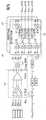
도 5는 도 4의 수신부(200)를 구체적으로 보여주는 도이고, 도 6은 도 5의 아날로그 전단부(210)를 구체적으로 나타내는 도이다.FIG. 5 is a diagram specifically illustrating the
도 4 내지 도 6을 참조하면, 아날로그 전단부(210)는 선형 등화기(211)와 가변 이득 증폭기(213)를 포함할 수 있다.4 to 6 , the
먼저, 선형 등화기(211)는 송신부(100)로부터 복수의 와이어들(W1~W4)을 통해 수신받은 변조 신호(AMBMCMDM)를 선형적으로 등화할 수 있다.First, the
다음으로, 가변 이득 증폭기(213)는 제1 내지 제4 메인 트랜지스터(TM1~TM4)를 포함할 수 있다.Next, the
구체적으로, 제1 메인 트랜지스터(TM1)는 메인 전류원(IMAIN)을 통해 변조 신호(AMBMCMDM) 중 제1 변조 비트(AM)를 제1 비교 입력(DA)으로 증폭시킬 수 있다. 또한, 제2 메인 트랜지스터(TM2)는 메인 전류원(IMAIN)을 통해 변조 신호(AMBMCMDM) 중 제2 변조 비트(BM)를 제2 비교 입력(DB)으로 증폭시킬 수 있다. 제3 메인 트랜지스터(TM3)는 메인 전류원(IMAIN)을 통해 변조 신호(AMBMCMDM) 중 제3 변조 비트(CM)를 제3 비교 입력(DC)으로 증폭시킬 수 있다. 또한, 제4 메인 트랜지스터(TM4)는 메인 전류원(IMAIN)을 통해 변조 신호(AMBMCMDM) 중 제4 변조 비트(DM)를 제4 비교 입력(DD)으로 증폭시킬 수 있다.Specifically, the first main transistor (TM1) which includes a main current source (IMAIN) a modulation signal (AM BM CM DM) the first modulated bit (AM) of the first comparison input (DA) of the through can be amplified with In addition, the second main transistor TM2 receives the second modulation bit BM of the modulation signal AM BM CM DM through the main current source IMAIN as the second comparison input DB . can be amplified. Third main transistor (TM3) is amplified by the third comparison input (DC) of a third modulated bit (CM) of a modulation signal (AM BM CM DM) via a main current source (IMAIN) can In addition, the fourth main transistor TM4 receives the fourth modulation bit DM of the modulation signal AM BM CM DM through the main current source IMAIN as the fourth comparison input DD . can be amplified.
즉, 가변 이득 증폭기(213)는 선형 등화기(211)를 통해 선형적으로 등화된 변조 신호(예컨대,DA.DB,DC,DD)에 기초하여, 메인 전류원(IMAIN)을 통해 변조 신호(AMBMCMDM)를 증폭시킬 수 있다. 이때, 가변 이득 증폭기(213)와 선형 등화기(211)의 입출력단의 개수는 복수의 와이어들(W1~W4)의 개수와 동일할 수 있다.That is, the
도 7은 도 5의 판정 궤환 등화부(230)를 구체적으로 나타내는 도이다.FIG. 7 is a diagram specifically illustrating the
도 4, 도 5 및 도 7을 참조하면, 판정 궤환 등화부(230)는 결정 장치(231)와 판정 궤환 등화기(233)를 포함할 수 있다.4, 5, and 7 , the
먼저, 결정 장치(231)는 복수의 비교기들(231_1~231_6)을 이용하여 가변 이득 증폭기(2130)를 통해 증폭된 변조 신호 예컨대, 제1 내지 제4 비교 입력(DADBDCDD)을 한쌍씩 비교하고, 상기 비교 결과에 기초하여 복수의 결정 값들(A-B, A-C, A-D, B-C, B-D, C-D)을 출력할 수 있다.First, the
다음으로, 판정 궤환 등화기(233)는 결정 장치(231)로부터 피드백받는 복수의 결정 값들(A-B, A-C, A-D, B-C, B-D, C-D) 중 적어도 셋 이상의 결정 값들에 기초하여, 제1 내지 제4 브런치 회로(233_1~233_4)에 병렬로 연결된 탭 전류원(ITAP)을 통해 변조 신호(예컨대, 가변 이득 증폭기(213)를 통해 증폭된 신호인 DADBDCDD)를 등화할 수 있다.Next, the
구체적으로, 제1 브런치 회로(233_1)는 제1 메인 트랜지스터(TM1)와 탭 전류원(ITAP)을 스위칭 연결할 수 있다. 또한, 제2 브런치 회로(233_2)는 제2 메인 트랜지스터(TM2)와 탭 전류원(ITAP)을 스위칭 연결할 수 있다. 또한, 제3 브런치 회로(233_3)는 제3 메인 트랜지스터(TM3)와 탭 전류원(ITAP)을 스위칭 연결할 수 있다. 또한, 제4 브런치 회로(233_4)는 제4 메인 트랜지스터(TM4)와 탭 전류원(ITAP)을 스위칭 연결할 수 있다.Specifically, the first branch circuit 233_1 may switch-connectthe first main transistor T M1 and the tap current source ITAP. In addition, the second branch circuit 233_2 may switch-connectthe second main transistor T M2 and the tap current source ITAP. In addition, the third branch circuit 233_3 may switch-connectthe third main transistor T M3 and the tap current source ITAP . In addition, the fourth branch circuit 233_4 may switch-connectthe fourth main transistor T M4 and the tap current source ITAP .
이때, 제1 내지 제4 브런치 회로(233_1~233_4) 각각은 탭 전류원(ITAP)에 병렬로 연결되는 적어도 셋 이상의 탭 트랜지스터들을 포함할 수 있다.In this case, each of the first to fourth branch circuits 233_1 to 233_4 may include at least three or more tap transistors connected in parallel to thetap current source I TAP .
도 8은 도 5의 디코딩부(230)를 구체적으로 나타내는 도이다.FIG. 8 is a diagram specifically illustrating the
도 4, 도 5 및 도 8을 참조하면, 디코딩부(230)는 제1 내지 제4 디코더(231~234)를 포함할 수 있다.4, 5 and 8 , the
실시예에 따른 제1 내지 제4 디코더(231~234)는 복수의 결정 값들(A-B, A-C, A-D, B-C, B-D, C-D) 중 적어도 일부(A-B, A-D, B-C, C-D)에 기초하여, 디지털 출력 신호(ABCD)를 디코딩할 수 있다.The first to
구체적으로, 제1 디코더(231)는 적어도 일부(A-B, A-D, B-C, C-D)의 어느 한쌍의 결정 값(A-D, A-B) 중 나머지 결정 값(A-C, B-D)에 따라 선택되는 제1 결정 값(예컨대, A-D)을 디지털 출력 신호(ABCD)의 제1 출력 신호(A)로 출력할 수 있다.Specifically, the
또한, 제2 디코더(232)는 적어도 일부(A-B, A-D, B-C, C-D)의 나머지 한쌍의 결정 값(C-D, B-C) 중 나머지 결정 값(A-C, B-D)에 따라 선택되는 제2 결정 값(예컨대, C-D)을 디지털 출력 신호(ABCD)의 제2 출력 신호(B)로 출력할 수 있다.In addition, the
또한, 제3 디코더(233)는 적어도 일부(A-B, A-D, B-C, C-D)의 나머지 한쌍의 결정 값(C-D, B-C) 중 나머지 결정 값(A-C, B-D)에 따라 선택되는 제3 결정 값(예컨대, B-C)을 디지털 출력 신호(ABCD)의 제3 출력 신호(C)로 출력할 수 있다.In addition, the
또한, 제4 디코더(234)는 적어도 일부(A-B, A-D, B-C, C-D)의 어느 한쌍의 결정 값(A-D, A-B) 중 나머지 결정 값(A-C, B-D)에 따라 선택되는 제4 결정 값(예컨대, A-B)을 디지털 출력 신호(ABCD)의 제4 출력 신호(D)로 출력할 수 있다.In addition, the
이러한 제1 내지 제4 디코더(231~234) 각각은 나머지 결정 값(A-C, B-D)에 따라 스위칭 온되는 제1 내지 제3 스위치(SW1~SW3)와 스위칭 오프되는 제4 내지 제6 스위치(SW4~SW6)로 구성될 수 있다.Each of the first to
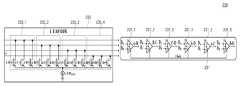
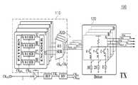
도 9는 본 출원의 다른 실시예에 따른 PAM-4 기반의 유선 트랜시버(11)에 대한 블록도이고, 도 10은 도 9의 송신부(100)를 구체적으로 보여주는 도이며, 도 11은 도 10의 인코딩부(110)에 기설정된 인코딩 맵핑 테이블(410)을 설명하기 위한 도이고, 도 12는 도 10의 드라이버부(120)에 기설정된 인코딩 로직 테이블(420)을 설명하기 위한 도이다.9 is a block diagram of a PAM-4 based wired
도 9와 도 10을 참조하면, PAM-4 기반의 유선 트랜시버(11)는 송신부(100)와 수신부(200)를 포함할 수 있다. 이하, 도 1 내지 도 8을 참조하여 설명된 동일한 부재번호의 송신부(100)와 수신부(200)에 대한 중복된 설명은 생략될 것이다.9 and 10 , the PAM-4 based wired
먼저, 송신부(100)는 송신 신호(ABCD)에 따라 인코딩된 변조 신호(AMBMCMDM)에 기초하여, 변조 신호(AMBMCMDM)의 각 출력 전압(V1, V2, V3, V4)을 조절 할 수 있다.First, the
또한, 송신부(100)는 변조 신호(AMBMCMDM)의 각 출력 전압(V1, V2, V3, V4)을 복수의 와이어들(W1~W4)을 통해 수신부(200)로 출력할 수 있다.In addition, the
다음으로, 수신부(200)는 변조 신호(AMBMCMDM)의 각 출력 전압(V1, V2, V3, V4)에 기초하여, 변조 신호(ATBTCTDT)로부터 결정되는 복수의 결정 값들(A-B, A-C, A-D, B-C, B-D, C-D) 중 적어도 일부(A-B, A-D, B-C, C-D)를 디지털 출력 신호(ABCD)로 출력할 수 있다.Next, the receiving
구체적으로, 송신부(100)는 인코딩부(110)와 드라이버부(120)를 포함할 수 있다.Specifically, the
먼저, 인코딩부(110)는 기설정된 인코딩 맵핑 테이블을 이용하여, 송신 신호(ABCD)를 변조 신호(AMBMCMDM)로 인코딩할 수 있다.First, the
도 11에 도시된 바와 같이, 기설정된 인코딩 맵핑 테이블(410)은 송신 신호(ABCD)와 변조 신호(AMBMCMDM)가 기설정된 경우의 수에 따라 컬럼 라인 별로 맵핑된 테이블일 수 있다. 예를 들면, 송신 신호(ABCD) '(1010)'는 변조 신호(AMBMCMDM) '(2301)'에 맵핑될 수 있다.As shown in FIG. 11 , the preset encoding mapping table 410 is a table mapped for each column line according to the number of cases in which thetransmission signal ABCD and the modulation signal A M BM CM DM are preset. can For example, the transmission signal ABCD '1010' may be mapped to themodulation signal A M BM CM DM '2301'.
다음으로, 드라이버부(120)는 기설정된 인코딩 로직 테이블(420)에 기초하여, 변조 신호(AMBMCMDM)에 대응되는 각 출력 전압(V1, V2, V3, V4)을 생성하고, 복수의 와이어들(W1~W4)을 통해 이를 출력할 수 있다.Next, the
도 12에 도시된 바와 같이, 기설정된 인코딩 로직 테이블(420)은 변조 신호(AMBMCMDM)의 각 신호 별로 기설정된 출력 전압(V1, V2, V3, V4)을 조절하기 위한 로직 값들(ENCX, ENCY, ENCZ)을 포함하는 테이블일 수 있다. 여기서, 기설정된 인코딩 로직 테이블(420)은 로직 값들(ENCX, ENCY, ENCZ)을 연산하기 위한 연산식들을 더 포함할 수 있다.12, the preset encoding logic table 420 is for adjusting the preset output voltages V1, V2, V3, and V4 for each signalof the modulation signal A M BM CM DM. It may be a table including logical values ENCX , ENCY , and ENCZ . Here, the preset encoding logic table 420 may further include arithmetic expressions for calculating thelogic values ENC X , ENCY , and ENCZ .
도 13은 도 10의 드라이버부(120)를 구체적으로 보여주는 도이고, 도 14는 도 13의 드라이버부(130)의 동작 예이다.13 is a diagram specifically illustrating the
먼저, 도 13을 참조하면, 드라이버부(120)는 와이어 별로 개별적으로 수신부(200)에 연결되는 복수의 송신 드라이버들(121~124)을 포함할 수 있다.First, referring to FIG. 13 , the
복수의 송신 드라이버들(121~124) 각각은 제1 내지 제3 송신 트랜지스터(TTX1, TTX2, TTX3)를 포함할 수 있다.Each of the plurality of
구체적으로, 제1 송신 트랜지스터(TTX1)는 일측에 제1 전류원(I)이 연결되고, 제2 송신 트랜지스터(TTX2)는 일측에 제2 전류원(2I)이 연결되며, 제3 트랜지스터(TTX3)는 일측에 제3 전류원(3I)이 연결될 수 있다. 또한, 제1 내지 제3 트랜지스터(TTX1, TTX2, TTX3)는 하나의 와이어 라인에 대해 타측으로 서로 병렬 연결될 수 있다.Specifically, the first transmission transistor TTX1 has a first current source I connected to one side, the second transmission transistor TTX2 has a second current source 2I connected to one side thereof, and the third transistor TTX3 ) may be connected to a third current source 3I on one side. Also, the first to third transistors TTX1 , TTX2 , and TTX3 may be connected to each other in parallel to the other side of one wire line.
여기서, 제1 내지 제3 전류원(I~3I)은 서로 다른 크기의 전류를 제공할 수 있다.Here, the first to third current sources I to 3I may provide currents of different magnitudes.
실시예에 따른 복수의 송신 드라이버들(121~124)은 기설정된 인코딩 로직 테이블에 따라, 제1 내지 제3 송신 트랜지스터(TTX1, TTX2, TTX3)에 대한 스위칭 온오프 동작을 수행할 수 있다. 이때, 복수의 송신 드라이버들(121~124)은 제1 내지 제3 전류원(I~3I) 중 어느 하나를 복수의 와이어들(W1~W4) 중 어느 하나의 와이어에 스위칭 연결할 수 있다.The plurality of
예를 들면, 도 14(a)에 도시된 바와 같이, 송신 신호(ABCD)가 '(1010)'인 CASE 1의 경우, 먼저, 인코딩부(110)는 기설정된 인코딩 맵핑 테이블(410)에 따라 송신 신호 '(1010)'을 변조 신호 '(2301)'로 인코딩할 수 있다. 이때, 복수의 송신 드라이버들(121~124) 중 제1 송신 드라이버(121)는 제1 전류원(I)을 제1 와이어(W1)에 연결하고, 제2 송신 드라이버(122)는 스위칭 오프되며, 제3 송신 드라이버(123)는 제3 전류원(3I)을 제3 와이어(W3)에 연결하고, 제4 드라이버(124)는 제2 전류원(2I)을 제4 와이어(W4)에 연결할 수 있다.For example, as shown in FIG. 14( a ), in case of
또한, 도 14(b)에 도시된 바와 같이, 송신 신호(ABCD)가 '(0101)'인 CASE 2의 경우, 인코딩부(110)는 기설정된 인코딩 맵핑 테이블에 따라 송신 신호 '(0101)'을 변조 신호 '(1032)'로 인코딩할 수 있다. 이때, 복수의 송신 드라이버들(121~124) 중 제1 송신 드라이버(121)는 제2 전류원(2I)을 제1 와이어(W1)에 연결하고, 제2 송신 드라이버(121)는 제3 전류원(3I)을 제2 와이어(W2)에 연결하며, 제3 송신 드라이버(123)는 스위칭 오프되고, 제4 드라이버(124)는 제1 전류원(I)을 제4 와이어(W4)에 연결할 수 있다.In addition, as shown in FIG. 14(b) , in case of
즉, 복수의 송신 드라이버들(121~124)은 제1 내지 제3 전류원(I~3I)을 통해 변조 신호(AMBMCMDM)에 대응되는 각 출력 전압(V1, V2, V3, V4)을 복수의 와이어들(W1~W4)을 통해 수신부(200)로 전송할 수 있다.That is, the plurality of
도 15는 도 1의 PAM-4 기반의 유선 트랜시버(10)와 종래의 트랜시버들과의 기술적 효과 차이를 나타내는 도이다.15 is a diagram illustrating a difference in technical effects between the PAM-4 based wired
도 15에 도시된 바와 같이, 종래의 싱글단 PAM-4 트랜시버(3)는 하나의 와이어 마다 2비트의 데이터를 송수신함으로써, 핀 효율성이 싱글단 NRZ 트랜시버(1) 대비 200%일 수 있다. 그러나, 종래의 싱글단 PAM-4 트랜시버(3)는 복수의 결정 값들을 결정하기 위한 적어도 하나의 문턱 전압은 3개가 필요함으로써, 종래의 싱글 PAM-4 트랜시버(3)는 싱글단 NRZ 트랜시버(1) 대비 약 6배 감소된 약 0.16 비율의 전압 마진을 가질 수 있다.As shown in FIG. 15 , the conventional single-ended PAM-4
실시예에 따른 PAM-4 기반의 유선 트랜시버(10)는 4개의 와이어마다 4비트를 송수신함으로써, 핀 효율성이 싱글단 NRZ 트랜시버(1) 대비 100%로 동일할 수 있다. 또한, PAM-4 기반의 유선 트랜시버(10)는 복수의 결정 값들을 결정하기 위한 적어도 하나의 문턱 전압을 이용하지 않으므로, 적어도 하나의 문턱 전압을 설정하는 동작을 스킵할 수 있어, 종래의 싱글단 PAM-4 트랜시버(3) 대비 4배 및 종래의 차동 PAM-4 트랜시버(4) 대비 2배 증가된 약 0.66 비율의 전압마진을 가질 수 있다.The PAM-4 based wired
본 출원은 도면에 도시된 일 실시 예를 참고로 설명되었으나 이는 예시적인 것에 불과하며, 본 기술 분야의 통상의 지식을 가진 자라면 이로부터 다양한 변형 및 균등한 타 실시 예가 가능하다는 점을 이해할 것이다. 따라서, 본 출원의 진정한 기술적 보호 범위는 첨부된 등록청구범위의 기술적 사상에 의해 정해져야 할 것이다. Although the present application has been described with reference to an embodiment shown in the drawings, this is merely exemplary, and those of ordinary skill in the art will understand that various modifications and equivalent other embodiments are possible therefrom. Accordingly, the true technical protection scope of the present application should be determined by the technical spirit of the appended claims.
10: PAM-4 기반의 유선 트랜시버
100: 송신부
200: 수신부10: Wired transceiver based on PAM-4
100: transmitter
200: receiver
Claims (20)
Translated fromKorean상기 변조 신호로부터 기설정된 디코딩 테이블을 통해 결정되는 복수의 결정 값들에 기초하여, 디지털 출력 신호를 생성하는 수신부를 포함하고,
상기 송신부와 상기 수신부는 상기 복수의 와이어들을 통해 서로 연결되고,
상기 수신부는 상기 송신부로부터 상기 복수의 와이어들을 통해 상기 변조 신호를 수신하는 아날로그 전단부를 포함하며,
상기 아날로그 전단부는 상기 송신부로부터 각 와이어를 통해 상기 변조 신호를 수신받는 선형 등화기; 및
상기 선형 등화기를 통해 선형 등화된 상기 변조 신호에 기초하여, 메인 전류원을 통해 상기 변조 신호를 증폭시키는 가변 이득 증폭기를 포함하는, PAM-4 기반의 유선 트랜시버.a transmitter for transmitting a modulated signal; and
a receiving unit that generates a digital output signal based on a plurality of determination values determined through a predetermined decoding table from the modulated signal;
The transmitter and the receiver are connected to each other through the plurality of wires,
The receiver includes an analog front end for receiving the modulated signal from the transmitter through the plurality of wires,
The analog front end unit includes: a linear equalizer receiving the modulated signal from the transmitter through each wire; and
and a variable gain amplifier for amplifying the modulated signal through a main current source based on the modulated signal linearly equalized through the linear equalizer.
상기 변조 신호는 단위 시간 마다 서로 다른 전압 레벨을 가지는 제1 내지 제4 변조 비트를 포함하는, PAM-4 기반의 유선 트랜시버.According to claim 1,
The modulation signal includes first to fourth modulation bits having different voltage levels for each unit time, a PAM-4 based wired transceiver.
상기 제1 내지 제4 변조 비트는 상기 복수의 와이어들 각각에 일대일 대응되는, PAM-4 기반의 유선 트랜시버.According to claim 1,
The first to fourth modulation bits correspond to each of the plurality of wires one-to-one, PAM-4 based wired transceiver.
상기 기설정된 디코딩 테이블은, 상기 변조 신호에 대한 경우의 수가 맵핑된 변조 비트 테이블, 상기 복수의 결정 값들에 대한 경우의 수가 맵핑된 결정값 테이블 및 상기 디지털 출력 신호에 대한 경우의 수가 맵핑된 출력 비트 테이블을 포함하고,
상기 변조 비트 테이블, 상기 결정값 테이블 및 상기 출력 비트 테이블은 컬럼 라인 별로 서로 대응되는, PAM-4 기반의 유선 트랜시버.According to claim 1,
The predetermined decoding table includes a modulation bit table to which the number of cases for the modulated signal is mapped, a decision value table to which the number of cases for the plurality of decision values is mapped, and an output bit to which the number of cases for the digital output signal is mapped. contains a table,
The modulation bit table, the decision value table, and the output bit table correspond to each other for each column line, a PAM-4 based wired transceiver.
상기 수신부는
상기 변조 신호를 비교하고, 상기 비교 결과에 기초하여 상기 변조 신호를 등화하는 판정 궤환 등화부; 및
상기 기설정된 디코딩 테이블을 이용하여, 상기 복수의 결정 값들 중 적어도 일부 값들을 상기 디지털 출력 신호로 디코딩하는 디코딩부를 더 포함하는, PAM-4 기반의 유선 트랜시버.According to claim 1,
the receiving unit
a decision feedback equalizer that compares the modulated signals and equalizes the modulated signals based on a result of the comparison; and
The PAM-4 based wired transceiver further comprising a decoding unit for decoding at least some of the plurality of determination values into the digital output signal by using the preset decoding table.
상기 선형 등화기와 상기 가변 이득 증폭기의 입출력단 개수는 상기 와이어의 개수와 동일한, PAM-4 기반의 유선 트랜시버.6. The method of claim 5,
The number of input and output terminals of the linear equalizer and the variable gain amplifier is the same as the number of wires, a PAM-4 based wired transceiver.
상기 가변 이득 증폭기는 상기 변조 신호 중 제1 변조 비트를 증폭하기 위한 제1 메인 트랜지스터;
상기 변조 신호 중 제2 변조 비트를 증폭하기 위한 제2 메인 트랜지스터;
상기 변조 신호 중 제3 변조 비트를 증폭하기 위한 제3 메인 트랜지스터; 및
상기 변조 신호 중 제4 변조 비트를 증폭하기 위한 제4 메인 트랜지스터를 포함하는, PAM-4 기반의 유선 트랜시버.6. The method of claim 5,
The variable gain amplifier may include a first main transistor for amplifying a first modulated bit of the modulated signal;
a second main transistor for amplifying a second modulated bit of the modulated signal;
a third main transistor for amplifying a third modulated bit of the modulated signal; and
A PAM-4 based wired transceiver comprising a fourth main transistor for amplifying a fourth modulated bit of the modulated signal.
상기 판정 궤환 등화부는, 상기 가변 이득 증폭기로부터 증폭되는 상기 변조 신호를 입력받아 상기 복수의 결정 값들을 판정하는 결정 장치; 및
상기 복수의 결정 값들 중 적어도 셋 이상의 결정 값들에 기초하여, 탭 전류원을 통해 상기 변조 신호를 등화하는 판정 궤환 등화기를 포함하는, PAM-4 기반의 유선 트랜시버.9. The method of claim 8,
The decision feedback equalizer may include: a decision unit configured to receive the modulated signal amplified from the variable gain amplifier and determine the plurality of decision values; and
and a decision feedback equalizer for equalizing the modulated signal through a tap current source based on at least three or more of the plurality of decision values.
상기 판정 궤환 등화기는 상기 제1 메인 트랜지스터와 상기 탭 전류원을 스위칭 연결하는 제1 브런치 회로;
상기 제2 메인 트랜지스터와 상기 탭 전류원을 스위칭 연결하는 제2 브런치 회로;
상기 제3 메인 트랜지스터와 상기 탭 전류원을 스위칭 연결하는 제3 브런치 회로; 및
상기 제4 메인 트랜지스터와 상기 탭 전류원을 스위칭 연결하는 제4 브런치 회로를 포함하는, PAM-4 기반의 유선 트랜시버.10. The method of claim 9,
The decision feedback equalizer includes: a first branch circuit that switches and connects the first main transistor and the tap current source;
a second branch circuit for switching the second main transistor and the tap current source;
a third branch circuit for switching the third main transistor and the tap current source; and
A wired transceiver based on PAM-4 comprising a fourth branch circuit for switching the fourth main transistor and the tap current source.
상기 제1 내지 제4 브런치 회로 각각은 상기 탭 전류원에 병렬로 연결되는 적어도 셋 이상의 탭 트랜지스터를 포함하는, PAM-4 기반의 유선 트랜시버.11. The method of claim 10,
Each of the first to fourth branch circuits includes at least three or more tap transistors connected in parallel to the tap current source.
상기 디코딩부는 상기 복수의 결정 값들 중 나머지 결정 값들에 기초하여, 상기 적어도 일부 값들을 상기 디지털 출력 신호들로 디코딩하는 제1 내지 제4 디코더를 포함하는, PAM-4 기반의 유선 트랜시버.6. The method of claim 5,
The decoding unit includes first to fourth decoders for decoding the at least some values into the digital output signals based on the remaining determined values among the plurality of determined values.
상기 제1 내지 제4 디코더 각각은 상기 나머지 결정 값들에 따라 스위칭 온되는 제1 내지 제3 스위치; 및
스위칭 오프되는 제4 내지 제6 스위치를 포함하는, PAM-4 기반의 유선 트랜시버.13. The method of claim 12,
Each of the first to fourth decoders includes first to third switches switched on according to the remaining determined values; and
A wired transceiver based on PAM-4, including fourth to sixth switches that are switched off.
상기 변조 신호의 각 출력 전압에 기초하여, 상기 변조 신호로부터 결정되는 복수의 결정 값들 중 적어도 일부를 디지털 출력 신호로 디코딩하는 수신부를 포함하고,
상기 송신부는 상기 변조 신호의 각 출력 전압을 복수의 와이어들을 통해 상기 수신부로 출력하고,
상기 수신부는 상기 송신부로부터 상기 복수의 와이어들을 통해 상기 변조 신호를 수신하는 아날로그 전단부를 포함하며,
상기 아날로그 전단부는 상기 송신부로부터 각 와이어를 통해 상기 변조 신호를 수신받는 선형 등화기; 및
상기 선형 등화기를 통해 선형 등화된 상기 변조 신호에 기초하여, 메인 전류원을 통해 상기 변조 신호를 증폭시키는 가변 이득 증폭기를 포함하는, PAM-4 기반의 유선 트랜시버.a transmission unit for adjusting each output voltage of the encoded modulated signal according to the transmission signal; and
a receiving unit for decoding at least a portion of a plurality of determined values determined from the modulated signal into a digital output signal based on each output voltage of the modulated signal;
The transmitter outputs each output voltage of the modulated signal to the receiver through a plurality of wires,
The receiver includes an analog front end for receiving the modulated signal from the transmitter through the plurality of wires,
The analog front end unit includes: a linear equalizer receiving the modulated signal from the transmitter through each wire; and
and a variable gain amplifier for amplifying the modulated signal through a main current source based on the modulated signal linearly equalized through the linear equalizer.
상기 송신부는 기설정된 인코딩 맵핑 테이블에 기초하여, 상기 송신 신호를 상기 변조 신호로 인코딩하는 인코딩부; 및
기설정된 인코딩 로직 테이블에 기초하여, 상기 변조 신호에 대응되는 각 출력 전압을 생성하는 드라이버부를 포함하는, PAM-4 기반의 유선 트랜시버.15. The method of claim 14,
The transmitting unit may include: an encoding unit encoding the transmission signal into the modulated signal based on a preset encoding mapping table; and
A PAM-4 based wired transceiver comprising a driver unit generating each output voltage corresponding to the modulated signal based on a preset encoding logic table.
기설정된 인코딩 맵핑 테이블은 상기 송신 신호와 변조 신호가 기설정된 경우의 수에 따라 컬럼 라인 별로 맵핑된 테이블인, PAM-4 기반의 유선 트랜시버.16. The method of claim 15,
The preset encoding mapping table is a table in which the transmission signal and the modulated signal are mapped for each column line according to a preset number of cases.
상기 기설정된 인코딩 로직 테이블은 상기 변조 신호의 각 신호 별로 기설정된 출력 전압을 조절하기 위한 로직 값들을 포함하는 테이블로서, 상기 로직 값들을 연산하기 위한 연산식들을 포함하는, PAM-4 기반의 유선 트랜시버.16. The method of claim 15,
The preset encoding logic table is a table including logic values for adjusting a preset output voltage for each signal of the modulated signal, and includes arithmetic expressions for calculating the logic values, a PAM-4 based wired transceiver .
상기 드라이버부는 와이어 마다 개별적으로 연결되는 송신 드라이버를 복수개 포함하고,
상기 송신 드라이버는,
제1 전류원이 일측에 연결되는 제1 트랜지스터;
제2 전류원이 일측에 연결되는 제2 트랜지스터; 및
제3 전류원이 일측에 연결되는 제3 트랜지스터를 포함하고,
상기 제1 내지 제3 트랜지스터는 하나의 와이어 라인에 대해 타측으로 서로 병렬로 연결되고,
상기 제1 내지 제3 전류원은 서로 다른 크기의 전류를 제공하는, PAM-4 기반의 유선 트랜시버.16. The method of claim 15,
The driver unit includes a plurality of transmission drivers individually connected to each wire,
The transmission driver is
a first transistor connected to one side of a first current source;
a second transistor connected to one side of a second current source; and
A third current source comprising a third transistor connected to one side,
The first to third transistors are connected in parallel to each other on the other side of one wire line,
The first to third current sources provide currents of different magnitudes, PAM-4 based wired transceivers.
상기 송신 드라이버는 상기 기설정된 인코딩 로직 테이블에 따라, 상기 제1 내지 제3 송신 트랜지스터에 대한 스위칭 온오프 동작을 통해, 상기 제1 내지 제3 전류원 중 어느 하나를 상기 복수의 와이어들 중 어느 하나에 연결하는, PAM-4 기반의 유선 트랜시버.19. The method of claim 18,
The transmission driver connects any one of the first to third current sources to any one of the plurality of wires through switching on/off operations for the first to third transmission transistors according to the preset encoding logic table. Connecting, PAM-4 based wired transceiver.
상기 송신부와 상기 수신부는 상기 복수의 결정 값들을 결정하기 위한 적어도 하나의 문턱 전압을 설정하는 동작을 스킵하는, PAM-4 기반의 유선 트랜시버.
14. The method of claim 13,
The transmitting unit and the receiving unit skip the operation of setting at least one threshold voltage for determining the plurality of determination values, a PAM-4 based wired transceiver.
Priority Applications (1)
| Application Number | Priority Date | Filing Date | Title |
|---|---|---|---|
| KR1020200084682AKR102266069B1 (en) | 2020-07-09 | 2020-07-09 | Wireline transceiver based on pulse amplitude modulation-4 |
Applications Claiming Priority (1)
| Application Number | Priority Date | Filing Date | Title |
|---|---|---|---|
| KR1020200084682AKR102266069B1 (en) | 2020-07-09 | 2020-07-09 | Wireline transceiver based on pulse amplitude modulation-4 |
Publications (1)
| Publication Number | Publication Date |
|---|---|
| KR102266069B1true KR102266069B1 (en) | 2021-06-18 |
Family
ID=76623233
Family Applications (1)
| Application Number | Title | Priority Date | Filing Date |
|---|---|---|---|
| KR1020200084682AActiveKR102266069B1 (en) | 2020-07-09 | 2020-07-09 | Wireline transceiver based on pulse amplitude modulation-4 |
Country Status (1)
| Country | Link |
|---|---|
| KR (1) | KR102266069B1 (en) |
Citations (3)
| Publication number | Priority date | Publication date | Assignee | Title |
|---|---|---|---|---|
| KR20170040304A (en)* | 2014-08-01 | 2017-04-12 | 칸도우 랩스 에스에이 | Orthogonal differential vector signaling codes with embedded clock |
| KR20180087472A (en)* | 2016-01-22 | 2018-08-01 | 마이크론 테크놀로지, 인크. | Apparatus and method for encoding and decoding signal lines for a multi-level communication architecture |
| KR20200016399A (en)* | 2017-08-07 | 2020-02-14 | 마이크론 테크놀로지, 인크 | Multi-level signaling in memory with wide system interface |
- 2020
- 2020-07-09KRKR1020200084682Apatent/KR102266069B1/enactiveActive
Patent Citations (3)
| Publication number | Priority date | Publication date | Assignee | Title |
|---|---|---|---|---|
| KR20170040304A (en)* | 2014-08-01 | 2017-04-12 | 칸도우 랩스 에스에이 | Orthogonal differential vector signaling codes with embedded clock |
| KR20180087472A (en)* | 2016-01-22 | 2018-08-01 | 마이크론 테크놀로지, 인크. | Apparatus and method for encoding and decoding signal lines for a multi-level communication architecture |
| KR20200016399A (en)* | 2017-08-07 | 2020-02-14 | 마이크론 테크놀로지, 인크 | Multi-level signaling in memory with wide system interface |
Similar Documents
| Publication | Publication Date | Title |
|---|---|---|
| US8588280B2 (en) | Asymmetric communication on shared links | |
| US7180957B2 (en) | Technique for utilizing spare bandwidth resulting from the use of a transition-limiting code in a multi-level signaling system | |
| US6556628B1 (en) | Methods and systems for transmitting and receiving differential signals over a plurality of conductors | |
| KR102257233B1 (en) | Pulse amplitude modulation-3 transceiver based on ground referenced signaling and operation method thereof | |
| KR102203390B1 (en) | Apparatus and method for single-ended pulse amplitude modulation-3 signaling | |
| US9215116B2 (en) | Method, transmitter and receiver device for transmitting a binary digital transmit signal over an optical transmission link | |
| US9853642B1 (en) | Data-dependent current compensation in a voltage-mode driver | |
| US6643471B2 (en) | Increased transmission capacity for a fiber-optic link | |
| JP2019527983A (en) | Voltage mode driver impedance and swing control | |
| US10171274B2 (en) | Data transmission apparatus, data reception apparatus, data transmission and reception system | |
| US8942309B1 (en) | Signal output improvement using data inversion and/or swapping | |
| JPH0879186A (en) | Optical transmitter circuit, optical receiver circuit, and optical transmitter / receiver circuit | |
| US7551897B1 (en) | Method and apparatus for performing transmit pre-emphasis | |
| US20050053171A1 (en) | Systems for data transmission | |
| KR102266069B1 (en) | Wireline transceiver based on pulse amplitude modulation-4 | |
| US7027522B2 (en) | Systems for data transmission | |
| KR20200001198A (en) | Decision feedback equalizer circuit | |
| CN111510175A (en) | Multi-channel transceiver structure | |
| US9210011B2 (en) | Push-pull source-series terminated transmitter apparatus and method | |
| US20220311649A1 (en) | Vector signaling code with improved noise margin | |
| KR102636015B1 (en) | Pam-8 transceiver using differential mode pam-4 and common mode nrz and transceive method therefor | |
| US10749526B1 (en) | Driver device | |
| US11088878B2 (en) | Transceiver using multi-level braid signaling and method of operating the same | |
| KR20250088387A (en) | Pam-3 transceiver including multiple equalization methods for multi-voltage levels | |
| KR102491784B1 (en) | Duo-binary receiver and transceiver with ground-referenced signaling |
Legal Events
| Date | Code | Title | Description |
|---|---|---|---|
| PA0109 | Patent application | Patent event code:PA01091R01D Comment text:Patent Application Patent event date:20200709 | |
| PA0201 | Request for examination | ||
| PE0902 | Notice of grounds for rejection | Comment text:Notification of reason for refusal Patent event date:20210401 Patent event code:PE09021S01D | |
| E701 | Decision to grant or registration of patent right | ||
| PE0701 | Decision of registration | Patent event code:PE07011S01D Comment text:Decision to Grant Registration Patent event date:20210604 | |
| GRNT | Written decision to grant | ||
| PR0701 | Registration of establishment | Comment text:Registration of Establishment Patent event date:20210611 Patent event code:PR07011E01D | |
| PR1002 | Payment of registration fee | Payment date:20210614 End annual number:3 Start annual number:1 | |
| PG1601 | Publication of registration | ||
| PR1001 | Payment of annual fee | Payment date:20240604 Start annual number:4 End annual number:4 |