KR102264728B1 - Deposition apparatus including an isothermal processing zone - Google Patents
Deposition apparatus including an isothermal processing zoneDownload PDFInfo
- Publication number
- KR102264728B1 KR102264728B1KR1020140083260AKR20140083260AKR102264728B1KR 102264728 B1KR102264728 B1KR 102264728B1KR 1020140083260 AKR1020140083260 AKR 1020140083260AKR 20140083260 AKR20140083260 AKR 20140083260AKR 102264728 B1KR102264728 B1KR 102264728B1
- Authority
- KR
- South Korea
- Prior art keywords
- faceplate
- backing plate
- isothermal
- defining
- contact
- Prior art date
- Legal status (The legal status is an assumption and is not a legal conclusion. Google has not performed a legal analysis and makes no representation as to the accuracy of the status listed.)
- Active
Links
Images


Classifications
- H—ELECTRICITY
- H01—ELECTRIC ELEMENTS
- H01J—ELECTRIC DISCHARGE TUBES OR DISCHARGE LAMPS
- H01J37/00—Discharge tubes with provision for introducing objects or material to be exposed to the discharge, e.g. for the purpose of examination or processing thereof
- H01J37/32—Gas-filled discharge tubes
- H01J37/32431—Constructional details of the reactor
- H01J37/3244—Gas supply means
- H01J37/32449—Gas control, e.g. control of the gas flow
- C—CHEMISTRY; METALLURGY
- C23—COATING METALLIC MATERIAL; COATING MATERIAL WITH METALLIC MATERIAL; CHEMICAL SURFACE TREATMENT; DIFFUSION TREATMENT OF METALLIC MATERIAL; COATING BY VACUUM EVAPORATION, BY SPUTTERING, BY ION IMPLANTATION OR BY CHEMICAL VAPOUR DEPOSITION, IN GENERAL; INHIBITING CORROSION OF METALLIC MATERIAL OR INCRUSTATION IN GENERAL
- C23C—COATING METALLIC MATERIAL; COATING MATERIAL WITH METALLIC MATERIAL; SURFACE TREATMENT OF METALLIC MATERIAL BY DIFFUSION INTO THE SURFACE, BY CHEMICAL CONVERSION OR SUBSTITUTION; COATING BY VACUUM EVAPORATION, BY SPUTTERING, BY ION IMPLANTATION OR BY CHEMICAL VAPOUR DEPOSITION, IN GENERAL
- C23C16/00—Chemical coating by decomposition of gaseous compounds, without leaving reaction products of surface material in the coating, i.e. chemical vapour deposition [CVD] processes
- C23C16/44—Chemical coating by decomposition of gaseous compounds, without leaving reaction products of surface material in the coating, i.e. chemical vapour deposition [CVD] processes characterised by the method of coating
- C23C16/455—Chemical coating by decomposition of gaseous compounds, without leaving reaction products of surface material in the coating, i.e. chemical vapour deposition [CVD] processes characterised by the method of coating characterised by the method used for introducing gases into reaction chamber or for modifying gas flows in reaction chamber
- C23C16/45563—Gas nozzles
- C23C16/45565—Shower nozzles
- C—CHEMISTRY; METALLURGY
- C23—COATING METALLIC MATERIAL; COATING MATERIAL WITH METALLIC MATERIAL; CHEMICAL SURFACE TREATMENT; DIFFUSION TREATMENT OF METALLIC MATERIAL; COATING BY VACUUM EVAPORATION, BY SPUTTERING, BY ION IMPLANTATION OR BY CHEMICAL VAPOUR DEPOSITION, IN GENERAL; INHIBITING CORROSION OF METALLIC MATERIAL OR INCRUSTATION IN GENERAL
- C23C—COATING METALLIC MATERIAL; COATING MATERIAL WITH METALLIC MATERIAL; SURFACE TREATMENT OF METALLIC MATERIAL BY DIFFUSION INTO THE SURFACE, BY CHEMICAL CONVERSION OR SUBSTITUTION; COATING BY VACUUM EVAPORATION, BY SPUTTERING, BY ION IMPLANTATION OR BY CHEMICAL VAPOUR DEPOSITION, IN GENERAL
- C23C16/00—Chemical coating by decomposition of gaseous compounds, without leaving reaction products of surface material in the coating, i.e. chemical vapour deposition [CVD] processes
- C23C16/44—Chemical coating by decomposition of gaseous compounds, without leaving reaction products of surface material in the coating, i.e. chemical vapour deposition [CVD] processes characterised by the method of coating
- C23C16/50—Chemical coating by decomposition of gaseous compounds, without leaving reaction products of surface material in the coating, i.e. chemical vapour deposition [CVD] processes characterised by the method of coating using electric discharges
- C23C16/505—Chemical coating by decomposition of gaseous compounds, without leaving reaction products of surface material in the coating, i.e. chemical vapour deposition [CVD] processes characterised by the method of coating using electric discharges using radio frequency discharges
- C23C16/509—Chemical coating by decomposition of gaseous compounds, without leaving reaction products of surface material in the coating, i.e. chemical vapour deposition [CVD] processes characterised by the method of coating using electric discharges using radio frequency discharges using internal electrodes
Landscapes
- Chemical & Material Sciences (AREA)
- Engineering & Computer Science (AREA)
- Chemical Kinetics & Catalysis (AREA)
- General Chemical & Material Sciences (AREA)
- Materials Engineering (AREA)
- Mechanical Engineering (AREA)
- Metallurgy (AREA)
- Organic Chemistry (AREA)
- Physics & Mathematics (AREA)
- Plasma & Fusion (AREA)
- Analytical Chemistry (AREA)
- Chemical Vapour Deposition (AREA)
- Condensed Matter Physics & Semiconductors (AREA)
- General Physics & Mathematics (AREA)
- Manufacturing & Machinery (AREA)
- Computer Hardware Design (AREA)
- Microelectronics & Electronic Packaging (AREA)
- Power Engineering (AREA)
Abstract
Translated fromKorean
Description
Translated fromKorean본 발명은 화학적 증착을 수행하기 위한 장치와 관련된 것이고, 박막의 플라즈마 강화된 화학적 증착을 수행하는데 특별한 유용성을 발견할 수도 있다.The present invention relates to an apparatus for performing chemical vapor deposition, and may find particular utility in performing plasma enhanced chemical vapor deposition of thin films.
플라즈마 처리 장치는 에칭, 물리적 기상 증착 (PVD), 화학적 기상 증착 (CVD), 플라즈마 강화된 화학적 기상 증착 (PECVD), 원자층 증착 (ALD), 플라즈마 강화된 원자층 증착 (PEALD), 펄싱된 (pulsed) 증착 층 (PDL), 플라즈마 강화된 펄싱된 증착 층 (PEPDL) 처리, 및 레지스트 제거를 포함하는 기법들에 의해 반도체 기판들을 처리하는데 이용된다. 플라즈마 처리에서 이용되는 플라즈마 처리 장치의 하나의 타입은 상단 전극 및 하단 전극을 포함하는 반응기 챔버를 포함한다. 무선 주파수 (RF) 전력은 반응기 챔버 내에서 반도체 기판들을 처리하기 위해 처리 가스를 플라즈마로 여기시키도록 전극들 사이에 인가된다. 이러한 챔버들에서, 반도체 기판에 걸친 불균일한 가열은 불균일한 기판 처리를 초래할 수 있다.Plasma processing devices include etching, physical vapor deposition (PVD), chemical vapor deposition (CVD), plasma enhanced chemical vapor deposition (PECVD), atomic layer deposition (ALD), plasma enhanced atomic layer deposition (PEALD), pulsed ( pulsed) deposition layer (PDL), plasma enhanced pulsed deposition layer (PEPDL) processing, and resist removal are used to process semiconductor substrates. One type of plasma processing apparatus used in plasma processing includes a reactor chamber containing a top electrode and a bottom electrode. Radio frequency (RF) power is applied between the electrodes to excite a process gas into a plasma to treat semiconductor substrates within the reactor chamber. In such chambers, non-uniform heating across the semiconductor substrate can result in non-uniform substrate processing.
본 명세서에는 반도체 기판들을 처리하기 위한 증착 장치가 개시되어 있고, 증착 장치는 등온 처리 존 (isothermal processing zone) 을 갖는다. 증착 장치는 반도체 기판들이 처리되는 화학적 격리 챔버를 포함한다. 처리 가스 소스는 처리 가스를 화학적 격리 챔버로 공급하기 위해 화학적 격리 챔버와 유체 연통하고, 샤워헤드 모듈은 처리 가스 소스로부터 등온 처리 존으로 처리 가스들을 전달한다. 샤워헤드 모듈은 페이스플레이트의 하부 면이 등온 처리 존을 정의하는 캐비티 (cavity) 의 상부 벽을 형성하는 페이스플레이트, 백킹 플레이트, 격리링이 백킹 플레이트를 지지하고 페이스플레이트 및 백킹 플레이트를 둘러싸는 격리링, 페이스플레이트를 백킹 플레이트로 부착하는 지지 엘리먼트, 및 페이스플레이트와 백킹 플레이트 사이에 중앙 가스 플리넘 (plenum) 의 외측 주위부 (perimeter) 를 형성하는 적어도 하나의 압축 실 (seal) 을 포함한다. 지지 엘리먼트와 페이스플레이트 사이의 접촉 면적은 페이스플레이트의 총 표면적의 1% 미만이다. 기판 페데스탈 (pedestal) 모듈은 반도체 기판을 가열하고 지지하도록 구성되고, 페데스탈 모듈의 상부 면은 화학적 격리 챔버 내에서 등온 처리 존을 정의하는 캐비티의 하부 벽을 형성하고, 배기 (evacuation) 장치는 처리 존으로부터 처리 가스를 배기 (evacuate) 하기 위해 등온 처리 존과 유체 연통한다.Disclosed herein is a deposition apparatus for processing semiconductor substrates, the deposition apparatus having an isothermal processing zone. The deposition apparatus includes a chemical isolation chamber in which semiconductor substrates are processed. The process gas source is in fluid communication with the chemical isolation chamber for supplying the process gas to the chemical isolation chamber, and the showerhead module delivers the process gases from the process gas source to the isothermal process zone. The showerhead module comprises a faceplate in which the lower face of the faceplate forms an upper wall of a cavity defining an isothermal treatment zone, a backing plate, an isolation ring supporting the backing plate and enclosing the faceplate and backing plate. , a support element attaching the faceplate to the backing plate, and at least one compression seal defining an outer perimeter of a central gas plenum between the faceplate and the backing plate. The contact area between the support element and the faceplate is less than 1% of the total surface area of the faceplate. A substrate pedestal module is configured to heat and support a semiconductor substrate, an upper surface of the pedestal module forms a lower wall of a cavity defining an isothermal processing zone within the chemical isolation chamber, and an evacuation device configured to heat the processing zone in fluid communication with the isothermal treatment zone to evacuate a process gas from the
또한, 본 명세서에는 플라즈마 처리 장치의 샤워헤드 모듈이 개시된다. 샤워헤드 모듈은 처리 가스들을 처리 가스 소스로부터 등온 처리 존으로 전달한다. 샤워헤드 모듈은 페이스플레이트의 하부 면이 등온 처리 존을 정의하는 캐비티의 상부 벽을 형성하는 페이스플레이트, 백킹 플레이트, 격리링이 백킹 플레이트를 지지하는 페이스플레이트 및 백킹 플레이트를 둘러싸는 격리 링, 페이스플레이트를 백킹 플레이트로 부착하는 지지 엘리먼트, 및 페이스플레이트와 백킹 플레이트 사이에 중앙 가스 플리넘의 외측 주위부를 형성하는 적어도 하나의 압축 실을 포함한다. 지지 엘리먼트와 페이스플레이트 사이의 접촉 면적은 페이스플레이트의 총 표면적의 1% 미만이다.Also disclosed herein is a showerhead module of a plasma processing apparatus. The showerhead module delivers process gases from the process gas source to the isothermal process zone. The showerhead module comprises a faceplate in which the lower face of the faceplate forms an upper wall of a cavity defining an isothermal treatment zone, a faceplate in which the isolation ring supports the backing plate and an isolation ring surrounding the backing plate, the faceplate a support element attaching to the backing plate, and at least one compression seal defining an outer perimeter of the central gas plenum between the faceplate and the backing plate. The contact area between the support element and the faceplate is less than 1% of the total surface area of the faceplate.
도 1은 본 명세서에 개시된 실시예들에 따른 화학적 증착 장치의 개요를 보이는 개략도를 도시한다.
도 2는 플라즈마가 박막들의 발생 동안 반응 종들 사이에서 증착 및/또는 표면 반응을 강화하는데 활용될 수 있는 본 명세서에 개시된 실시예들을 구현하기 위해 배열된 다양한 장치 컴포넌트들을 묘사한 블록도를 도시한다.
도 3은 본 명세서에 개시된 실시예들에 따라 배열된 페데스탈 모듈 및 샤워헤드 모듈의 단면도를 도시한다.
도 4a 내지 도 4e는 본 명세서에 개시된 실시예들에 따라 배열된 샤워헤드 모듈의 단면도를 각각 도시한다.
도 5a 및 도 5b는 본 명세서에 개시된 실시예들에 따라 배열된 샤워헤드의 단면도를 각각 도시한다.
도 6은 본 명세서에 개시된 실시예들에 따라 배열된 샤워헤드 모듈의 단면도를 도시한다.1 shows a schematic diagram showing an overview of a chemical vapor deposition apparatus according to embodiments disclosed herein.
2 shows a block diagram depicting various apparatus components arranged to implement embodiments disclosed herein in which plasma may be utilized to enhance deposition and/or surface reaction between reactive species during generation of thin films.
3 shows a cross-sectional view of a pedestal module and showerhead module arranged in accordance with embodiments disclosed herein.
4A-4E each show cross-sectional views of a showerhead module arranged in accordance with embodiments disclosed herein.
5A and 5B respectively show cross-sectional views of a showerhead arranged in accordance with embodiments disclosed herein.
6 shows a cross-sectional view of a showerhead module arranged in accordance with embodiments disclosed herein.
이하의 상세한 설명에서, 다수의 특정한 실시예들이 본 명세서에 개시된 장치 및 방법의 충분한 이해를 제공하기 위해 설명된다. 그러나, 본 실시예들이 이 특정한 세부사항들 없이 또는 대체의 엘리먼트 또는 처리를 이용함으로써 실시될 수도 있다는 것은 당업자에게 명백할 것이다. 다른 예시들에서, 잘 알려진 처리, 절차, 및/또는 컴포넌트들은 본 명세서에 개시된 실시예들의 양태를 불필요하게 모호히 하지 않도록 상세히 기술되지 않았다. 본 명세서에 이용된 것으로서, 용어 "약"은 ± 10% 를 나타낸다.In the following detailed description, a number of specific embodiments are set forth in order to provide a thorough understanding of the apparatus and methods disclosed herein. However, it will be apparent to one skilled in the art that the present embodiments may be practiced without these specific details or by using alternative elements or processes. In other instances, well-known processes, procedures, and/or components have not been described in detail so as not to unnecessarily obscure aspects of the embodiments disclosed herein. As used herein, the term “about” refers to ±10%.
보여진 바와 같이, 본 실시예들은 플라즈마 강화된 화학적 기상 증착과 같은 화학적 증착을 수행하기 위한 장치 및 관련된 방법을 제공한다. 장치 및 방법은, 이들로 제한되지는 않으나, 복수-단계 증착 처리 (예컨대, 원자층 증착 (ALD)), 플라즈마 강화된 원자층 증착 (PEALD), 플라즈마 강화된 화학적 기상 증착 (PECVD), 펄싱된 증착 층 (PDL), 또는 플라즈마 강화된 펄싱된 증착 층 (PEPDL) 처리) 내에서 자기-제한 (self-limiting) 증착 단계들의 분리를 요구하는 유전체 증착처리를 기초로 하는 반도체 제조와 함께 이용되기 위해 특히 적용 가능하다.As shown, the present embodiments provide apparatus and related methods for performing chemical vapor deposition, such as plasma enhanced chemical vapor deposition. The apparatus and method include, but are not limited to, a multi-step deposition process (eg, atomic layer deposition (ALD)), plasma enhanced atomic layer deposition (PEALD), plasma enhanced chemical vapor deposition (PECVD), pulsed For use with semiconductor fabrication based on dielectric deposition processes that require separation of self-limiting deposition steps within a deposition layer (PDL), or plasma enhanced pulsed deposition layer (PEPDL) process) Especially applicable.
전술된 처리들은 증착된 물질을 수용하는 웨이퍼 또는 기판에 걸친 불균일한 온도와 관련된 몇몇의 결점 (drawback) 으로 악화된다. 예를 들어, 불균일한 온도는 주변 챔버 컴포넌트들과 열적으로 접촉하는 수동적으로 가열된 샤워헤드가 주변 컴포넌트들로 열을 잃는 경우 기판에 걸쳐 나타날 수도 있다. 따라서, 처리 존의 상부 벽을 형성하는 샤워헤드는 바람직하게는 등온 처리 존이 형성될 수도 있도록 주변 컴포넌트로부터 열적으로 격리되고, 이로써 기판에 걸쳐 균일한 온도를 그리고 샤워헤드 정면 (face) (즉, 처리 존의 상부 벽) 에 걸쳐 균일한 온도를 형성한다. 기판에 걸친 균일한 온도는 반도체 기판의 균일한 처리를 지원하고, 기판 온도는 증착 처리를 위한 활성화 에너지를 제공하므로 증착 반응을 구동하기 위한 제어 수단이다. 또한, 샤워헤드에 걸친 균일한 온도는 반도체 기판 위에 균일한 가스 페이즈 반응을 지원한다. 또한, 균일한 온도는 더 낮은 열 전도도를 갖지만 더 높은 내식성 (corrosion resistance) 을 갖는 재료의 선택을 지원한다.The processes described above are exacerbated by some drawback related to non-uniform temperature across the wafer or substrate containing the deposited material. For example, a non-uniform temperature may appear across the substrate when a passively heated showerhead in thermal contact with the surrounding chamber components loses heat to the surrounding components. Accordingly, the showerhead forming the upper wall of the treatment zone is preferably thermally isolated from surrounding components such that an isothermal treatment zone may be formed, thereby providing a uniform temperature across the substrate and the showerhead face (i.e., to create a uniform temperature across the upper wall of the treatment zone). A uniform temperature across the substrate supports uniform processing of the semiconductor substrate, and the substrate temperature is a control means for driving the deposition reaction as it provides the activation energy for the deposition process. In addition, a uniform temperature across the showerhead supports a uniform gas phase response over the semiconductor substrate. The uniform temperature also supports the selection of materials with lower thermal conductivity but higher corrosion resistance.
또한, 일반적으로 증착 샤워헤드의 2개의 주된 타입이 있다 : 샹들리에 타입 및 플러쉬 마운트 (flush mount). 샹들리에 샤워헤드는 일 단부 상에 챔버의 상단에 부착되는 스템을 가지고 다른 단부 상에 페이스플레이트를 가지며, 샹들리에와 유사하다. 스템의 일부는 가스 라인들 및 RF 전력부의 연결이 가능하도록 챔버 상단에서 돌출될 수도 있다. 따라서, 샹들리에 설계에 의해 요구되는 것과 같이 처리 동안 배기되어야 (evacuated) 하는 더 큰 챔버 부피는 매우 과중한 처리량을 발생시킬 수 있다. 그러나, 플러시 마운트 샤워헤드는 챔버의 상단으로 통합되고 (integrated) 스템을 갖지 않으므로, 배기되어야 하는 챔버 부피가 감소될 수 있다. 본 명세서에 개시된 본 실시예들은 플러시 마운트 타입 샤워헤드에 관계하고, 플러시 마운트 샤워헤드는 처리 동안 진공 소스에 의해 배기되어야 하는 챔버 부피를 감소시킨다. 플러시 마운트 샤워헤드는 샤워헤드 정면 및 바디로부터 전도를 통해 챔버의 나머지로 열을 잃을 수 있다. 이는 샤워헤드의 페이스플레이트의 온도를 더 낮게할 뿐만 아니라, 처리 존에 노출된 샤워헤드 정면에 방사상의 온도 불균일성을 도입한다. 본 명세서에 개시된 실시예들은 샤워헤드로부터 챔버로의 전도를 통한 열 손실을 감소시키고, 처리 존에 노출된 샤워헤드의 정면의 방사상의 온도 균일성을 증가시키며, 이로써 등온 처리 존을 형성한다.Also, there are generally two main types of deposition showerheads: chandelier types and flush mounts. A chandelier showerhead is similar to a chandelier, having a stem attached to the top of the chamber on one end and a faceplate on the other end. A portion of the stem may protrude from the top of the chamber to allow connection of gas lines and RF power. Thus, a larger chamber volume that must be evacuated during processing, such as required by the chandelier design, can result in very heavy throughput. However, since the flush mount showerhead is integrated into the top of the chamber and has no stem, the chamber volume that must be evacuated can be reduced. The present embodiments disclosed herein relate to a flush mount type showerhead, which reduces the chamber volume that must be evacuated by the vacuum source during processing. A flush mount showerhead may lose heat from the showerhead front and body to the rest of the chamber through conduction. This not only lowers the temperature of the showerhead's faceplate, but also introduces a radial temperature non-uniformity in the showerhead face exposed to the treatment zone. Embodiments disclosed herein reduce heat loss through conduction from the showerhead to the chamber and increase the radial temperature uniformity of the front face of the showerhead exposed to the treatment zone, thereby forming an isothermal treatment zone.
도 1은 본 명세서에 개시된 실시예들에 따른 화학적 증착 장치 (201) 의 개요를 도시하는 개략도이다. 기판 (13) 은 또한 수직으로 이동될 수도 있는 샤워헤드 모듈 (211) 에 대하여 상승되거나 하강될 수 있는 이동 가능한 페데스탈 모듈 (223) 의 상단 상에 놓인다. 반응 재료 가스들은 가스 라인 (203) 을 경유하여 챔버의 처리 존 (318) 으로 도입된다. 장치는 사용되는 반응 가스들의 수에 따라 일 이상의 가스 라인들을 갖도록 변경될 수도 있다는 것을 주목하라. 챔버는 진공 소스 (209) 와 연결되는 진공 라인들 (23) 을 통해 배기된다. 진공 소스는 진공 펌프일 수도 있다.1 is a schematic diagram illustrating an overview of a chemical vapor deposition apparatus 201 according to embodiments disclosed herein. A
본 명세서에 개시된 실시예들은 바람직하게는 플라즈마 강화된 화학적 증착 장치 (즉, PECVD 장치, PEALD 장치, 또는 PEPDL 장치) 내에 구현될 수 있다. 도 2는 플라즈마가 증착을 강화하는데 활용되는 본 명세서에 개시된 실시예들을 구현하기 위해 배열된 다양한 장치 컴포넌트들을 묘사한 간단한 블록도를 제공한다. 도시된 바와 같이, 처리 존 (318) 은 페데스탈 모듈 (223) 과 함께 작동하는 샤워헤드 모듈 (211) 을 포함하는 용량성 커플링된 플라즈마 시스템에 의해 발생되는 플라즈마를 포함하도록 하는 기능을 하고, 상기 플라즈마 시스템에서 페데스탈 모듈 (223) 은 가열된다. 매칭 네트워크 (206) 와 연결된 적어도 하나의 고-주파수 (HF) RF 발생기 (204) 및 선택적인 저-주파수 (LF) RF 발생기 (202) 와 같은 RF 소스(들)은 샤워헤드 모듈 (211) 과 연결된다. 대안적인 실시예에서, HF 발생기 (204) 는 페데스탈 모듈 (223) 과 연결될 수 있다. 매칭 네트워크 (206) 에 의해 공급되는 전력 및 주파수는 처리 가스/증기로부터 플라즈마를 발생시키기 충분하다. 일 실시예에서, HF 발생기 및 LF 발생기 양자가 이용되고, 대안적인 실시예에서는, HF 발생기만이 이용된다. 통상적인 처리에서, HF 발생기는 약 2 MHz 내지 100 MHz 의 주파수에서 통상적으로 동작되고; 바람직한 실시예에서는 13.56 MHz 또는 27 MHz 에서 동작된다. LF 발생기는 약 50 kHz 내지 2 MHz 에서 통상적으로 동작되고; 바람직한 실시예에서는 약 350 kHz 내지 600 kHz 에서 동작된다. 처리 파라미터들은 챔버 부피, 기판 사이즈, 및 다른 팩터들에 기반되어 스케일링 (scaling) 될 수도 있다. 유사하게, 처리 가스의 유속 (flow rate) 들은 진공 챔버 또는 처리 존의 자유 부피에 의존할 수도 있다.Embodiments disclosed herein may preferably be implemented within a plasma enhanced chemical vapor deposition apparatus (ie, a PECVD apparatus, a PEALD apparatus, or a PEPDL apparatus). 2 provides a simplified block diagram depicting various apparatus components arranged to implement embodiments disclosed herein in which plasma is utilized to enhance deposition. As shown,
챔버 내에서, 페데스탈 모듈 (223) 은 박막들과 같은 재료들이 증착될 수도 있는 기판 (13) 을 지지한다. 페데스탈 모듈 (223) 은 증착 및/또는 플라즈마 트리트먼트 반응들 동안 그리고 증착 및/또는 플라즈마 트리트먼트 반응들 간에 기판을 홀딩하고 이동시키도록 포크 또는 리프트 핀들을 포함할 수 있다. 일 실시예에서, 기판 (13) 은 페데스탈 모듈 (223) 의 표면 상에 위치되도록 구성될 수도 있으나, 대안적인 실시예들에서, 페데스탈 모듈 (223) 은 페데스탈 모듈 (223) 의 표면 상에 기판 (13) 을 홀딩하기 위해 정전 척, 기계적인 척, 또는 진공 척을 포함할 수도 있다. 페데스탈 모듈 (223) 은 목표된 온도로 기판 (13) 을 가열하기 위해 히터 블록 (220) 과 커플링될 수 있다. 통상적으로, 기판 (13) 은 증착되는 재료에 따라 약 25 ℃ 내지 500 ℃ 또는 더 큰 온도에서 유지된다.Within the chamber, a
특정 실시예들에서, 시스템 제어기 (228) 는 증착, 후 증착 트리트먼트들, 및/또는 다른 처리 동작들 동안 처리 조건들을 제어하도록 채용된다. 제어기 (228) 는 일 이상의 메모리 디바이스들 및 일 이상의 프로세서들을 통상적으로 포함할 것이다. 프로세서는 CPU 또는 컴퓨터, 아날로그 및/또는 디지털 입력/출력 연결들, 스테퍼 모터 제어기 보드들 (boards) 등을 포함할 수도 있다.In certain embodiments, the
특정 실시예들에서, 제어기 (228) 는 장치의 모든 활동들을 제어한다. 시스템 제어기 (228) 는 처리 동작들의 타이밍, LF 발생기 (202) 및 HF 발생기 (204) 의 동작의 주파수 및 전력, 전구체들 및 비활성 가스들의 유속 및 온도, 전구체들 및 비활성 가스들의 상대적 믹싱 (mixing), 히터 블록 (220) 및 샤워헤드 모듈 (211) 의 온도, 챔버의 압력, 및 특정 처리의 다른 파라미터들을 제어하기 위해 인스트럭션들의 세트들을 포함하는 시스템 제어 소프트웨어를 실행한다. 제어기와 관련된 메모리 디바이스들에 저장된 다른 컴퓨터 프로그램들은 몇몇의 실시예들에 채용될 수도 있다.In certain embodiments, the
통상적으로 제어기 (228) 와 관련된 사용자 인터페이스가 있을 것이다. 사용자 인터페이스는 디스플레이 스크린, 장치 및/또는 처리 조건들의 그래픽 소프트웨어 디스플레이들 (graphical software displays), 및 포인팅 디바이스들, 키보드들, 터치 스크린들, 마이크크로폰 등과 같은 사용자 입력 디바이스들을 포함할 수도 있다.There will typically be a user interface associated with the
비-일시적 컴퓨터 머신-판독가능한 매체는 장치의 제어를 위한 프로그램 인스트럭션들을 포함할 수 있다. 처리 동작들을 제어하기 위한 컴퓨터 프로그램 코드는 임의의 통상적 컴퓨터 판독가능한 프로그래밍 언어로 작성될 수 있다: 예를 들어, 어셈블리 언어, C, C++, 파스칼, 포트란 또는 다른 것들. 컴파일되는 오브젝트 코드 또는 스크립트는 프로그램 내에서 식별되는 태스크들을 수행하도록 프로세서에 의해 실행된다. 제어기 파라미터들은, 예를 들어, 처리 단계들의 타이밍, 전구체 및 비활성 가스들의 유속 및 온도, 웨이퍼의 온도, 챔버의 압력 및 특정 처리의 다른 파라미터들과 같은 처리 조건들에 관련한다. 이 파라미터들은 레시피의 형태로 사용자에게 제공되고 사용자 인터페이스를 활용하여 입력될 수도 있다.The non-transitory computer machine-readable medium may contain program instructions for controlling the apparatus. The computer program code for controlling the processing operations may be written in any conventional computer readable programming language: for example, assembly language, C, C++, Pascal, Fortran or others. The compiled object code or script is executed by the processor to perform the tasks identified within the program. Controller parameters relate to processing conditions such as, for example, the timing of processing steps, flow rates and temperatures of precursors and inert gases, temperature of the wafer, pressure in the chamber and other parameters of a particular processing. These parameters are provided to the user in the form of a recipe and may be input using a user interface.
처리를 모니터링하기 위한 신호들은 시스템 제어기의 아날로그 및/또는 디지털 입력 연결들에 의해 제공될 수도 있다. 처리를 제어하기 위한 신호들은 장치의 아날로그 및 디지털 출력 연결들 상에 출력된다.Signals for monitoring processing may be provided by analog and/or digital input connections of the system controller. Signals for controlling the processing are output on the analog and digital output connections of the device.
시스템 소프트웨어는 다수의 상이한 방식들로 구성되거나 설계될 수도 있다. 예를 들어, 다양한 챔버 컴포넌트 서브루틴들 또는 제어 오브젝트들은 증착 처리들을 수행하는데 필요한 챔버 컴포넌트들의 동작을 제어하도록 작성될 수도 있다. 이 목적을 위한 프로그램들 또는 프로그램들의 섹션들의 예시들은 처리 단계의 기판 타이밍 코드, 전구체 및 불활성 가스의 유속 및 온도 코드, 및 챔버의 압력에 대한 코드를 포함한다.The system software may be configured or designed in many different ways. For example, various chamber component subroutines or control objects may be written to control the operation of chamber components necessary to perform deposition processes. Examples of programs or sections of programs for this purpose include codes for substrate timing codes of processing steps, flow rates and temperature codes of precursors and inert gases, and codes for pressure in the chamber.
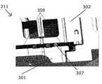
도 3은 도 1 및 도 2의 페데스탈 모듈 (223) 및 샤워헤드 모듈 (211) 을 포함하는 화학적 격리 챔버 (319) 의 단면도를 더 상세히 도시하고, 페데스탈 모듈 (223) 및 샤워헤드 모듈 (211) 은 반도체 기판이 처리되는 캐비티 (318) 를 형성한다. 캐비티 (318) 는 샤워헤드 (211) 와 페데스탈 모듈 (223) 사이에 형성되고, 샤워헤드 모듈 (211) 의 페이스플레이트 (301) 의 하부 면은 캐비티의 상부 벽 및 측벽을 형성하고, 페데스탈 모듈 (223) 의 상부 면은 캐비티 (318) 의 하부 벽을 형성한다. 듀얼 챔버 실들 (seals) 을 포함하는 증착 장치의 예시적인 실시예는 그것의 전부가 본 명세서에 참조로서 인용되는 공통 양도된 미국 특허 제 7,737,035 호에서 발견될 수 있다.3 shows in greater detail a cross-sectional view of a
페데스탈 모듈 (223) 은 하단 RF 전극 (317) 을 포함하고 기판 (13) 은 페데스탈 모듈 (223) 상에 놓인다. 바람직하게는 하단 RF 전극 (317) 은 접지된다. 처리 동안 기판 (13) 의 상단과 샤워헤드 모듈 (211) 의 하단 면 간의 거리는 바람직하게는 약 5 밀리미터 내지 16 밀리미터이다. 페데스탈 모듈 (223) 은 히터를 포함하고 (도 2 참조) 샤워헤드 모듈 (211) 의 페이스플레이트 (301) 는 처리 동안 페데스탈 모듈 (223) 로부터 릴리즈되는 열로부터 그리고 처리 동안 캐비티 (318) 내에서 타격되는 플라즈마에 의해 가열된다. 몇몇의 실시예들에서, 챔버 내부의 온도는 샤워헤드 모듈 (211) 및 페데스탈 모듈 (223) 내의 가열 메커니즘을 통해 유지될 수 있다. 바람직하게는, 기판 (13) 은 등온 환경 내에 위치된다. 등온 처리 존은 목표된 온도로 캐비티 (318) 의 노출된 표면 각각을 유지함으로써 형성된다. 등온 처리 존은 목표되지 않은 온도 구배가 기판 (13) 에 걸쳐 형성되지 않도록 기판 (13) 이 균일하게 가열되고 목표된 온도로 유지되도록 허용한다. 등온 처리 존을 형성하기 위해, 페이스플레이트 (301) 로부터 백킹 플레이트 (302) 로의 열 손실 및 페이스플레이트 (301) 로부터 격리 링 (303) 으로의 열 손실은 최소화된다. 일 실시예에서, 샤워헤드 모듈 (211) 은 약 250 ℃ 내지 500 ℃로 또는 약 500 ℃ 보다 더 큰 온도로 가열될 수 있다. 바람직한 실시예에서, 캐비티 (318) 의 노출된 표면 각각은 세라믹 재료로 형성된다.The
샤워헤드 모듈 (211) 은 페이스플레이트 (301), 백킹 플레이트 (302), 및 격리 링 (303) 을 포함하고, 격리 링은 페이스플레이트 (301) 및 백킹 플레이트 (302) 를 둘러싸고 백킹 플레이트 (302) 를 지지한다. 격리 링 (303) 은 바람직하게는 알루미늄 옥사이드 (Al2O3) 또는 알루미늄 나이트라이드 (AlN) 와 같은 세라믹 재료로 형성되고 화학적 격리 챔버 (319) 의 접지된 챔버 벽 (322) 상에서 지지될 수 있다.The
백킹 플레이트 (302) 는 금속 재료로 형성된다. 예를 들어, 백킹 플레이트는 Al 6061 과 같은 알루미늄 합금 또는 스테인리스 스틸로 형성될 수 있고, 백킹 플레이트 (302) 는 의도된 용도 (application) 에 따라 알루미늄 옥사이드 외측 코팅, 이트륨 옥사이드 외측 코팅, 또는 폴리머 코팅과 같은 세라믹 외측 코팅을 포함할 수 있다. 바람직한 실시예에서, 백킹 플레이트 (302) 는 RF가 흐르는데 (RF hot), 즉, RF 소스에 의해 전력을 공급받는다. 일 실시예에서, 백킹 플레이트 (302) 는 냉각된 백킹 플레이트일 수 있다. 페이스플레이트 (301) 는 바람직하게는 세라믹 또는 금속 재료로 형성되고, 바람직한 실시예들에서, 알루미늄 옥사이드 (Al2O3) 또는 알루미늄 나이트라이드 (AlN) 로 형성될 수 있다. 페이스플레이트 (301) 는 전기적으로 전도성일 수 있고 페이스플레이트 내에 매입된 (embedded) RF 전극 (310) 과 함께 세라믹 재료로 이루어질 수 있고, 매입된 RF 전극 (310) 은 바람직하게는 메쉬 전극이다. 가스 플리넘 (308) 은 페이스플레이트 (301) 와 백킹 플레이트 (302) 사이에 형성된다. 바람직하게는 페이스플레이트 (301) 와 백킹 플레이트 (302) 사이의 가스 플리넘 (308) 의 높이는 최소의 플리넘 (308) 부피를 제공하는 동안 플리넘 (308) 으로부터 캐비티 (318) 로 양호한 가스 흐름을 가능하게한다. 바람직하게는 플리넘 (308) 의 높이는 약 2 mm 내지 6 mm 이다. 적어도 하나의 RF 접촉부 (312) 는 백킹 플레이트 (302) 및 페이스플레이트 (301) 내에 매입된 RF 전극 (310) 과 전기적으로 연결된다. 일 실시예에서, RF 접촉부 (312) 는 적어도 하나의 벤드 (bend) 를 갖는 금속성 스트립으로 구성되는 환형 RF 접촉부일 수 있고, RF 접촉부 (312) 는 페이스플레이트 (301) 와 백킹 플레이트 (302) 사이에 가스 플리넘 (308) 의 외측 주위부를 형성한다. 바람직하게는 RF 접촉부 (312) 는 페이스플레이트 (301) 와 백킹 플레이트 (302) 사이에 열적 초크 (thermal choke) 를 형성한다.The
도 4a는 등온 처리 존을 형성하는 샤워헤드 모듈 (211) 및 기판 지지부 (223) 의 예시적인 실시예를 도시하고, 여기서 지지 엘리먼트는 샤워헤드 모듈의 페이스플레이트를 샤워헤드 모듈의 백킹 플레이트에 부착한다. 바람직하게는 등온 처리 존에 노출된 표면 각각은 목표된 온도로 유지되는 세라믹 표면이다. 샤워헤드 모듈 (211) 은 페이스플레이트의 하부 면이 등온 처리 존을 정의하는 캐비티 (318) 의 상부 벽 및 선택적으로 캐비티 (318) 의 측벽을 형성하는 페이스플레이트 (301), 백킹 플레이트 (302), 및 격리 링 (303) 이 페이스플레이트 (301) 및 백킹 플레이트 (302) 를 둘러싸는 격리 링 (303) 을 포함한다. 백킹 플레이트 (302) 는 일 이상의 가스 유입부들 (305) 및 일 이상의 가스 유출부들 (315) (도 4e 참조) 을 포함할 수 있고, 페이스플레이트 (301) 는 바람직하게는 등온 처리 존으로 처리 가스를 전달하거나, 등온 처리 존으로 비활성 가스를 전달하거나, 또는 등온 처리 존으로부터 처리 가스 및/또는 비활성 가스를 제거하기 위해 복수의 관통 홀들 (through holes) (304) 을 포함한다.4A shows an exemplary embodiment of a
예를 들어, 완전히 웨이퍼 위로 연장하는 페이스플레이트의 중앙 존은 처리 가스를 전달하고 등온 처리 존으로부터 반응된 가스를 인출하도록 동심의 가스 유입구들 및 가스 유출구들을 포함할 수 있다. 동심의 유입구들 및 유출구들의 적합한 배열은 본 명세서에 참조로서 인용되는 미국 특허 제 5,102,523 호 또는 제 5,614,026 호에 개시된다.For example, a central zone of the faceplate that extends completely above the wafer may include concentric gas inlets and gas outlets to deliver process gas and withdraw reacted gas from the isothermal processing zone. Suitable arrangements of concentric inlets and outlets are disclosed in US Pat. Nos. 5,102,523 or 5,614,026, which are incorporated herein by reference.
적어도 하나의 압축 실은 백킹 플레이트와 페이스플레이트 사이에 위치될 수 있고, 압축 실 각각은 적어도 하나의 가스 플리넘의 경계를 형성할 수 있다. 예를 들어, 2개의 압축 실들은 가스 플리넘들을 형성하는데 이용될 수 있고, 제1 압축 실은 페이스플레이트 (301) 와 백킹 플레이트 (302) 사이에서 압축되는 제1 환형 레버 실 (306a) 이고 제1 환형 레버 실 (306a) 은 내측 가스 플리넘 (308a) 를 형성한다. 내측 가스 플리넘 (308a) 은 관통 홀을 통해 처리 가스가 등온 처리 존을 정의하는 캐비티 (318) 로 전달될 수 있도록 백킹 플레이트 (302) 의 일 이상의 가스 유입부들 (305) 및 페이스플레이트 (301) 의 복수의 관통 홀들 (304) 과 유체 연통 할 수 있다. 제2 압축 실은 제1 환형 레버 실 (306a) 을 둘러싸고 페이스플레이트 (301) 과 백킹 플레이트 (302) 사이에서 압축되는 제2 환형 레버실 (306b) 일 수 있고, 제2 환형 레버실 (306b) 은 내측 가스 플리넘 (308a) 을 둘러싸는 중간 (intermediate) 플리넘 (308b) 을 형성한다. 중간 플리넘 (308b) 은 처리 가스가 진공 소스에 의해 캐비티 (318) 내에서 등온 처리 존으로부터 제거될 수 있도록 백킹 플레이트 (302) 의 일 이상의 가스 유출부들 (315) 및 페이스플레이트 (301) 의 복수의 관통 홀들 (302) 과 유체 연통 할 수 있다. 일 실시예에서, 외측 가스 플리넘 (308c) 은 중간 플리넘 (308b) 를 둘러싼다. 바람직하게는 외측 가스 플리넘 (308c) 은 캐비티 (318) 내에서 등온 처리 존과 유체 연통하는 격리 링 (303) 과 페이스플레이트 (301) 사이의 갭으로 처리 가스를 전달할 수 있고, 격리 링 (303) 은 외측 가스 플리넘 (308c) 의 외측 주변부를 형성한다. 바람직하게는 환형 레버 실 (306a, 306b) 각각은 페이스플레이트 (301) 및 백킹 플레이트 (302) 와 대향하는 스프링 힘을 제공하고, 레버 실 (306a, 306b) 각각은 페이스플레이트 (301) 와 접촉하는 하부 자유 단부와 백킹 플레이트 (302) 와 접촉하는 상부 자유 단부 사이의 약 0.5 인치 내지 1.5 인치의 길이 및 약 0.003 인치 내지 0.009 인치의 두께를 갖는 적어도 하나의 벤드 (bend) 를 갖는다. 바람직하게는 레버 실 (306a, 306b) 각각은 S-형상, C-형상, E-형상, Z-형상 또는 V-형상 단면을 가진다.At least one compression seal may be positioned between the backing plate and the faceplate, and each compression seal may define at least one gas plenum. For example, two compression seals may be used to form gas plenums, a first compression seal being a first
일 실시예에서, 페이스플레이트 (301) 는 복수의 캠 락 (cam lock) 어셈블리들 (309) 을 포함하는 지지 엘리먼트를 이용하여 백킹 플레이트 (302) 에 부착된다. 커플링되는 경우, 캠 락 어셈블리 (309) 각각은 페이스플레이트 (301) 와 백킹 플레이트 (302) 사이에 환형 레버 실 (306a, 306b) 을 압축하도록 구성된다. 압축된 환형 레버 실 (306a, 306b) 각각은 페이스플레이트 (301) 로부터 백킹 플레이트 (302) 로의 열 손실을 페이스플레이트 (301) 와 백킹 플레이트 (302) 사이에 가스 플리넘들 (308a, 308b, 308c) 을 형성하는 동안 최소화될 수도 있도록 페이스플레이트 (301) 와 백킹 플레이트 (302) 사이에 열적 초크 (choke) 를 형성한다.In one embodiment, the
캠 락 어셈블리 (309) 각각은 바람직하게는 소켓 (513) 으로 실장되는 (mounted) 스터드 (stud) (락킹 (locking) 핀) (505) 를 포함한다. 소켓 (513) 은 페이스플레이트 내에서 소켓 홀 (513a) 내에 실장될 수 있다. 일 실시예에서, 소켓 (513) 은 외부의 스레드들 (threads) 을 포함할 수 있고, 소켓 (513) 은 관련하는 내부의 스레드들을 갖는 소켓 홀 (513a) 으로 실장된다. 대안적으로, 소켓 (513) 은 소켓 홀 (513a) 로 본딩될 수도 있다. 캠 락 어셈블리 (309) 는 페이스플레이트 (301) 를 백킹 플레이트 (302) 로 빠르고, 청결하고, 정확하게 부착하는 것을 가능하게 한다. 스터드 (505) 는, 예를 들어, (니트로닉-60 (Nitronic-60) 과 같은) 스테인리스 스틸 또는 몰리브덴을 포함하는 금속 또는 금속 합금으로 형성될 수 있고, 예를 들어, 스테인리스 스틸 벨르빌레 (Belleville) 세척기들, 또는 헤인즈 242® (Haynes 242®) 와 같은 합금으로 형성되는 세척기들과 같은 디스크 스프링 스택 (disc spring stack) (515) 에 의해 둘러싸일 수도 있다. 스터드 (505) 및 디스크 스프링 스택 (515) 은 측방의 움직임의 양이 2개의 부품들 사이에서 열팽창 (thermal expansion) 의 차이들을 야기하기 위해 페이스플레이트 (301) 과 백킹 플레이트 (302) 사이에서 제한되는 것이 가능하도록 소켓 (513) 내에 배열된다.Each of the
캠 락 어셈블리 (309) 각각의 다른 부분들은 스터드 (505) 를 수용하도록 구성되는 백킹 플레이트 (302) 의 백킹 플레이트 보어 (bore) (511) 내에 실장되는 캠축 베어링 어셈블리 (507) 를 포함할 수 있다. 샤워헤드 모듈의 페이스플레이트를 샤워헤드 모듈의 백킹 플레이트와 커플링시키는데 이용될 수 있는 캠 락 어셈블리의 예시적인 실시예는 본 명세서에 그것의 전부가 참조로서 인용되는 공통 양도된 미국 특허 제 8,272,346 호 내에서 발견될 수 있다.The other portions of each of the
캠 락 어셈블리 (309) 각각은 RF 접촉부 (312) 를 형성하는 전기적으로 전도성인 소켓을 포함할 수 있고, RF 접촉부 (312) 는 RF가 흐르는 백킹 플레이트 (302) 와 페이스플레이트 (301) 의 RF 전극 (310) 을 전기적으로 연결한다. RF 접촉부 (312) 각각은 금속 또는 임의의 적합한 전도 물질로 형성될수 있으나, 바람직한 실시예에서, RF 접촉부 (312) 각각은 텅스텐으로 형성된다. 대안적으로, RF 접촉부 (312) 는 스테인리스 스틸 또는 오스테나이트 니켈-크롬 기반 합금 (austenitic nickel-chromium base alloy) 으로 형성될 수 있다. 또한, RF 접촉부 (312) 각각은 니켈 외측 코팅을 포함할 수 있다. 캠 락 어셈블리 (309) 각각은 바람직하게는 페이스플레이트 (301) 가 샤워헤드 모듈 (211) 의 나머지로부터 열적으로 격리될 수 있도록 페이스플레이트 (301) 과 백킹 플레이트 (302) 사이에 최소한의 접촉 면적을 제공한다. 샤워헤드 모듈 (211) 의 페이스플레이트 (301) 를 열적으로 격리시키는 것은 페이스플레이트의 상단 면으로부터 백킹 플레이트 (302) 로의 열 손실을 감소시킬 뿐만 아니라, 페이스플레이트의 외측 주변부에서 페이스플레이트 (301) 를 둘러싸는 격리 링 (303) 으로의 열 손실을 감소시키고, 이로써 캐비티 (318) 내에 등온 처리 존을 형성한다. 페이스플레이트 (301) 를 열적으로 격리시키는 것은 목표된 온도가 페이스플레이트 (301) 의 하부 면에 걸쳐 유지되도록 허용하고 더 균일한 기판 처리를 유도한다. 지지 엘리먼트 (캠 락) 와 페이스플레이트 사이의 접촉 면적은 페이스플레이트의 총 표면적의 1 % 미만이다. 바람직하게는 총 접촉 면적은 페이스플레이트의 총 표면적의 0.5 % 미만, 페이스플레이트의 총 표면적의 0.3 % 미만, 페이스플레이트의 총 표면적의 0.2 % 미만, 페이스플레이트의 총 표면적의 0.1 % 미만, 또는 페이스플레이트의 총 표면적의 0.05 % 미만이다. 도 4c에 도시된 바와 같이, RF 접촉부 (312) 는 캠 락 어셈블리 (309) 의 소켓을 형성할 수도 있고, RF 접촉부 (312) 의 하부 부분 312a) 은 페이스플레이트 (301) 와 백킹 플레이트 (302) 사이의 접촉 면적을 최소화하도록 페이스플레이트 (301) 내에 실장될 수 있고, 페이스플레이트와 백킹 플레이트 사이에서 감소된 열전사 (thermal transfer) 를 제공할 수 있다. RF 접촉부 (312) 의 하부 부분 (312a) 는 바람직하게는 매입된 RF 전극 (310) 으로 브레이징된다 (brazed).Each of the
도 4b는 향상된 RF 프로파일을 갖는 캐비티 (318) 내에 등온 처리 존을 형성하도록 구성되는 기판 지지부 (223) 및 샤워헤드 모듈 (211) 의 일 실시예를 도시한다. 도 4b에 도시된 바와 같이, 페데스탈 모듈 (223) 의 하단 RF 전극 (317) 은 캐비티 (318) 의 외측 주변부 너머로 또는 외측 주변부로 연장하도록 길어질 수 있다. 캐비티 (318) 의 주변부 너머로, 바람직하게는 접지된 전극인, 하단 RF 전극 (317) 을 연장하는 것은, 페데스탈 모듈과 둘러싸는 접지된 챔버 벽 (322) 사이의 아크방전에 대한 포텐셜이 또한 감소될 수 있도록, 페데스탈 모듈 (223) 과 둘러싸는 접지된 챔버 벽 (322) 사이의 전계의 강도를 감소시킨다. 바람직하게는, 하단 RF 전극 (317) 은 약 12.5 인치 보다 더 큰 직경을 갖고, 더 바람직하게는 하단 RF 전극 (317) 은 약 15.6 인치의 직경과 같은 약 15 인치보다 더 큰 직경을 갖는다.4B shows one embodiment of a
일 실시예에서, 도 4d에 도시된 바와같이, 격리 링 (303) 은 페이스플레이트 (301) 를 백킹 플레이트 (302) 로 부착하는 지지 엘리먼트를 포함하고, 페이스플레이트와 백킹 플레이트 사이의 환형 레버 실 (306a, 306b) 각각을 압축하고, 격리 링 (303) 은 페이스플레이트 (301) 의 외측 부분의 밑에 있는 내측 환형 플랜지 (313) 을 포함하고, 내측 환형 플랜지 (313) 는 페이스플레이트 (301) 를 지지하는 내측 환형 플랜지 상에 위치된 적어도 하나의 상향으로 연장하는 돌출부 (314) 를 갖는다. 적어도 하나의 상향으로 연장하는 돌출부 (314) 는 페이스플레이트 (301) 와 접촉하고 백킹 플레이트 (302) 에 대하여 페이스플레이트 (301) 를 바이어스시키는 (즉, 백킹 플레이트 (302) 와 평행한 페이스플레이트 (301) 를 유지하는) 열적 초크를 제공한다. 바람직하게는, 적어도 3개의 상향으로 연장하는 돌출부 (314) 가 페이스플레이트 (301) 를 지지한다. 적어도 하나의 상향으로 연장하는 돌출부 (314) 는, 페이스플레이트 (310) 가 페이스플레이트의 외측 주변부에서 격리 링 (303) 뿐만 아니라 샤워헤드 모듈 (211) 의 나머지로부터 열적으로 격리될 수도 있도록 격리 링 (303) 과 페이스플레이트 (301) 사이의 접촉 면적을 최소화한다. 페이스플레이트 (301) 를 샤워헤드 모듈 (211) 의 나머지로부터 열적으로 격리시키는 것은 캐비티 (318) 내에 더 균일한 기판 처리를 이끄는 등온 처리 존을 제공할 수 있다. 격리 링 (303) 의 적어도 하나의 상향으로 연장하는 돌출부 (314) 와 페이스플레이트 (301) 사이의 최대 총 접촉 면적은 약 0.05 in2 미만이고, 바람직하게는 약 0.02 in2 미만이고, 더 바람직하게는 약 0.01 in2 미만이다. 부착되는 경우, 격리 링 (303) 은 내측 가스 플리넘 (308a) 을 형성하기 위해 페이스플레이트 (301) 와 백킹 플레이트 (302) 사이에서 제1 환형 레버 실 (306a) 을 압축하도록, 그리고 중간 가스 플리넘 (308b) 을 형성하기 위해 제2 환형 레버 실 (306b) 를 압축하도록 구성된다. 일 실시예에서, 페이스플레이트 (301) 의 상부 면은 환형 리세스들 (360) 을 포함할 수 있고, 환형 레버 실 (306a, 306b) 각각의 하단 부분은 각각의 환형 리세스 (306) 내에 지지된다. 추가의 실시예에서, 백킹 플레이트 (302) 의 하부 면은 또한 환형 리세스들 (360) 을 포함할 수 있고, 환형 레버 실 (306a, 306b) 각각의 상부 부분은 각각의 환형 리세스 (360) 내에 지지된다. RF 접촉부 (312) 는 페이스플레이트 (301) 내에 매입된 RF 전극 (310) 을 RF가 흐르는 백킹 플레이트 (302) 와 전기적으로 연결한다. RF 접촉부 (312) 는 스테인리스 스틸, 텅스텐, 오스테나이트 니켈-크롬 기반된 합금과 같은 임의의 적합한 전도 재료로 형성될 수 있고, 바람직하게는 니켈 도금된 인코넬® (Inconel®) 등과 같은 외측 니켈 도금을 포함한다. 바람직한 실시예에서, RF 접촉부 (312) 는 적어도 하나의 벤드를 갖는 금속성 스트립으로 이루어진 환형 RF 접촉부이고, RF 접촉부는 세라믹 페이스플레이트 내에 매입된 RF 전극과 전기적으로 연결되고, 환형 RF 접촉부는 제2 환형 레버 실을 둘러싸고 백킹 플레이트 (302) 와 페이스플레이트 (301) 사이에 외측 가스 플리넘 (308c) 의 외측 주위부를 형성한다. 백킹 플레이트 (302) 내의 가스 유입부 (305) 는 비활성 가스를 외측 가스 플리넘 (308c) 으로 전달하도록 구성될 수 있고, 다음으로 비활성 가스는 외측 가스 플리넘 (308c) 과 유체 연통하는 페이스플레이트 (301) 내의 관통 홀들 (304) 을 경유하여 캐비티 (318) 의 외측 주변부로 전달된다. RF 접촉부 (312) 는 RF 접촉부 내에 압축가능한 적어도 하나의 벤드를 가지고, 벤드의 직경은 격리 링 (303) 의 내측 표면 (303a) 과 RF 접촉부 (312) 의 외측 표면 사이에서 아크방전에 대한 포텐셜을 최소화하도록 구성된다.In one embodiment, as shown in FIG. 4D , the
일 실시예에서, 도 4e에 도시된 바와 같이, 지지 엘리먼트는 페이스플레이트 (301) 를 백킹 플레이트 (302) 로 부착할 뿐만 아니라 페이스플레이트 (301) 를 백킹 플레이트 (302) 와 전기적으로 연결하는 RF 접촉부 (312) 를 포함한다. RF 접촉부 (312) 는 바람직하게는 적어도 하나의 벤드를 갖는 금속성 스트립으로 이루어진 환형 RF 접촉부이고, RF 접촉부 (312) 는 레버 실들 (306a, 306b) 을 압축하도록 페이스플레이트 (301) 과 백킹 플레이트 (302) 사이에 클램핑 힘을 제공한다. 적어도 하나의 벤드는 바람직하게는 격리 링 (303) 의 내측 표면 (303a) 와 RF 접촉부 (312) 의 외측 표면 사이에서 아크방전에 대한 포텐셜을 최소화하도록 구성되는 직경을 가진다. 환형 RF 접촉부 (312) 는 백킹 플레이트 (302) 와 페이스플레이트 (301) 사이에 외측 가스 플리넘 (308c) 의 외측 주변부를 형성한다. RF 접촉부 (312) 의 하부 단부는 바람직하게는 페이스플레이트 (301) 내에 매입된 RF 전극 (310) 의 노츨된 부분으로 브레이징되고, 한편 RF 접촉부 (312) 의 상부 단부는 바람직하게는, 스레디드 (threaded) 볼트, 스크류, 또는 이 밖의 유사한 것일 수 있는, 적합한 기계적 패스너들 (fasteners) (320) 로 백킹 플레이트 (302) 에 부착된다. 바람직한 실시예에서, 약 9개 내지 12개의 기계적 패스너들 (32) 이 RF 접촉부 (312) 의 상부 단부를 백킹 플레이트 (312) 에 부착할 수 있으나, 대안적인 실시예들에서, 더 많은 패스너들 (320) 이 활용될 수도 있다. RF 접촉부 (312) 는 바람직하게는 페이스플레이트와 접촉하는 하부 자유 단부와 백킹 플레이트와 접촉하는 상부 자유 단부사이에서 약 0.5 인치 내지 1.5 인치의 길이 및 약 0.003 인치 내지 0.009 인치의 두께를 갖는다. 바람직하게는, RF 접촉부는 S-형상, C-형상, E-형상, Z-형상 또는 V-형상 단면을 가진다. 부착되는 경우, RF 접촉부 (312) 는 페이스플레이트 (301) 과 백킹 플레이트 (302) 사이에서 환형 레버 실 (306a, 306b) 각각을 압축하고, RF 접촉부 (312) 는 제2 환형 레버 실 (306b) 을 둘러싸고 플리넘 (308c) 을 형성한다. RF 접촉부 (312) 는 페이스플레이트 (301) 의 RF 전극 (310) 을 RF가 흐르는 백킹 플레이트 (302) 와 전기적으로 연결한다. RF 접촉부 (312) 는 스테인리스 스틸, 텅스텐, 오스테나이트 니켈-크롬 기반된 합금과 같은 임의의 적합한 전도 재료로 형성될 수 있고, RF 접촉부 (312) 는 바람직하게는 니켈 도금된 인코넬® 및 이와 유사한 것과 같은 외측 니켈 도금을 포함한다.In one embodiment, as shown in FIG. 4E , the support element attaches the
페이스플레이트 (301) 는 바람직하게는 페이스플레이트의 외측 주변부에서 상부 표면 상에 적어도 하나의 상향으로 연장하는 스페이서 (307) (도 5a 참조) 를 포함하고, 적어도 하나의 상향으로 연장하는 스페이서 (307) 는 페이스플레이트 (301) 와 백킹 플레이트 (302) 사이에 목표된 플리넘 높이를 유지하고, 적어도 하나의 스페이서 (307) 는 백킹 플레이트 (302) 에 대해 평행한 페이스플레이트 (301) 를 유지하도록 구성된다. 바람직한 실시예에서, 적어도 3개의 상향으로 확장하는 스페이서들 (307) 이 페이스플레이트 (301) 와 백킹 플레이트 (302) 사이에 위치된다. 대안적인 실시예에서, 적어도 하나의 스페이서 (307) 는 하향으로 확장하는 방식으로 백킹 플레이트 (302) 의 하부 면 (302a) 상에 제공될 수 있다. 예를 들어, 스페이서 (307) 는 백킹 플레이트 (302) 의 하부 면 (302a) 으로 압축되는 사파이어 볼 (ball) 일 수 있다. 페이스플레이트 (301) 의 적어도 하나의 상향으로 연장하는 스페이서 (307) 와 백킹 플레이트 (302) 사이의 총 접촉 면적은 약 0.5 in2 미만, 바람직하게는 약 0.05 in2 미만, 더 바람직하게는 약 0.01 in2 미만이다.The
도 5b는 샤워헤드 모듈 (211) 의 일 실시예를 도시하고, 적어도 하나의 스페이서 (307) 는 페이스플레이트 (301) 와 백킹 플레이트 (302) 사이에 위치되고, 스페이서 (307) 는 페이스플레이트와 백킹 플레이트 사이에서 목표된 가스 플리넘 높이를 유지하고, 적어도 하나의 스페이서 (307) 는 백킹 플레이트 (302) 에 대하여 평행한 페이스플레이트 (301) 를 유지하도록 구성된다. 바람직하게는 적어도 3개의 스페이서들 (307) 이 페이스플레이트 (301) 과 백킹 플레이트 (302) 사이에 위치된다. 스페이서들 (307) 은 페이스플레이트 (301) 에 통합될 수 있고 (도 5a 참조), 또는 대안적으로 스페이서들 (307) 은 가스 플리넘 (308) 의 외측 주변부 내에 위치된 구체들 (spheres) 일 수 있고, 스페이서들 (307) 은, 페이스플레이트와 백킹 플레이트 사이의 목표된 플리넘 높이가 유지될 수도 있게끔 스페이서들이 페이스플레이트 (301) 및 백킹 플레이트 (302) 의 열팽창 및 열수축을 허용할 수도 있도록, 자유롭게 이동가능하다. 바람직하게는 스페이서들 (307) 은 세라믹 재료로 형성된다. 대안적인 바람직한 실시예에서, 스페이서들 (307) 은 석영 또는 사파이어로 형성될 수 있다.5B shows one embodiment of a
도 6은 샤워헤드 모듈 (211) 의 일 실시예를 도시하고, RF 접촉부 (312) 는 페이스플레이트 (301) 내에 매입된 RF 전극 (310) 과 전기적으로 연걸된 페이스플레이트 (301) 의 금속화된 표면 (301) 과 마찰 접촉을 형성하고, RF 접촉부 (312) 는 페이스플레이트 (301) 의 RF 전극 (310) 을 RF가 흐르는 백킹 플레이트 (302) 와 전기적으로 연결한다. 페이스플레이트 (301) 의 하부 면은 캐비티 (318) 의 상부 벽을 형성하고, 페이스플레이트 (301) 의 하부 면은 하부면의 외측 주변부 둘레에 유사한 재료의 링 (402) 을 포함하고, 링 (402) 의 내측 표면은 캐비티 (318) 내에 등온 처리 존을 정의하는 캐비티 (318) 의 측벽을 형성한다. 바람직하게는 링 (402) 은 페이스플레이트 (301) 의 하부 면에 스크류들 (403) 과 같은 적합한 패스너들에 의해 기계적으로 부착되거나 본딩된다.6 shows one embodiment of a
등온 처리 존을 포함하는 플라즈마 처리 장치가 그것의 특정한 실시예에 관련하여 상세히 기술되었으나, 첨부된 청구항의 범위로부터 벗어나지 않고 다양한 변화 및 변경이 이뤄질 수 있고 균등물들이 채용될수 있다는 것은 당업자에게 명백할 것이다.Although a plasma processing apparatus including an isothermal treatment zone has been described in detail with respect to specific embodiments thereof, it will be apparent to those skilled in the art that various changes and modifications may be made and equivalents may be employed without departing from the scope of the appended claims. .
Claims (20)
Translated fromKorean상기 반도체 기판들이 처리되는 화학적 격리 챔버 (chemical isolation chamber);
상기 화학적 격리 챔버로 처리 가스를 공급하기 위해 상기 화학적 격리 챔버와 유체 연통하는 처리 가스 소스;
상기 처리 가스 소스로부터 상기 등온 처리 존으로 처리 가스들을 전달하는 샤워헤드 모듈로서, 상기 샤워헤드 모듈은, 페이스플레이트 (faceplate) 로서, 상기 페이스플레이트의 하부 면은 상기 등온 처리 존을 정의하는 (defining) 캐비티 (cavity) 의 상부 벽을 형성하는, 상기 페이스플레이트; 백킹 플레이트 (backing plate); 상기 페이스플레이트 및 상기 백킹 플레이트를 둘러싸고, 상기 백킹 플레이트를 지지하는 격리 링; 상기 페이스플레이트를 상기 백킹 플레이트에 부착시키는 지지 엘리먼트 (element); 및 상기 페이스플레이트와 상기 백킹 플레이트 사이에 중앙 플리넘 (plenum) 의 외측 주위부 (perimeter) 를 형성하는 적어도 하나의 압축 실 (seal) 을 포함하고, 상기 지지 엘리먼트와 상기 페이스플레이트 사이의 접촉 면적은 상기 페이스플레이트의 총 표면적의 1% 미만인, 상기 샤워헤드 모듈; 및
반도체 기판을 가열하고 지지하도록 구성되는 기판 페데스탈 (pedestal) 모듈로서, 상기 페데스탈 모듈의 상부 면은 상기 화학적 격리 챔버 내에 상기 등온 처리 존을 정의하는 캐비티의 하부벽을 형성하는, 상기 페데스탈 모듈을 포함하고,
상기 적어도 하나의 압축 실은 제1 압축 실 및 제2 압축 실을 포함하고;
상기 제1 압축 실은 상기 페이스플레이트와 상기 백킹 플레이트 사이에서 압축되고, 상기 페이스플레이트와 상기 백킹 플레이트 사이에 내측 가스 플리넘을 형성하는 제1 환형 레버 실이고; 그리고
상기 제2 압축 실은 상기 페이스플레이트와 상기 백킹 플레이트 사이에서 압축되는 제2 환형 레버 실이고, 상기 제2 레버 실은 상기 제1 레버 실을 둘러싸고 상기 제2 레버 실은 상기 내측 가스 플리넘을 둘러싸는 중간 가스 플리넘을 형성하고, 외측 가스 플리넘은 상기 중간 가스 플리넘을 둘러싸는, 등온 처리 존을 갖는 반도체 기판들을 처리하기 위한 증착 장치.A deposition apparatus for processing semiconductor substrates having an isothermal processing zone, comprising:
a chemical isolation chamber in which the semiconductor substrates are processed;
a process gas source in fluid communication with the chemical isolation chamber for supplying a process gas to the chemical isolation chamber;
a showerhead module for delivering process gases from the process gas source to the isothermal processing zone, the showerhead module comprising: a faceplate, a lower surface of the faceplate defining the isothermal processing zone said faceplate forming an upper wall of a cavity; backing plate; an isolation ring surrounding the faceplate and the backing plate and supporting the backing plate; a support element attaching the faceplate to the backing plate; and at least one compression seal defining an outer perimeter of a central plenum between the faceplate and the backing plate, wherein the contact area between the support element and the faceplate is the showerhead module being less than 1% of the total surface area of the faceplate; and
a substrate pedestal module configured to heat and support a semiconductor substrate, wherein an upper surface of the pedestal module forms a lower wall of a cavity defining the isothermal processing zone within the chemical isolation chamber; and ,
said at least one compression chamber comprising a first compression chamber and a second compression chamber;
the first compression seal is a first annular lever seal compressed between the faceplate and the backing plate and forming an inner gas plenum between the faceplate and the backing plate; And
the second compression seal is a second annular lever seal compressed between the faceplate and the backing plate, the second lever seal surrounding the first lever seal and the second lever seal surrounding the inner gas plenum A deposition apparatus for processing semiconductor substrates having an isothermal processing zone forming a plenum, wherein an outer gas plenum surrounds the intermediate gas plenum.
상기 증착 장치는:
(a) 상기 등온 처리 존 내에서 상기 처리 가스를 플라즈마 상태로 에너자이징 (energizing) 하도록 구성되는 RF 에너지 소스;
(b) 상기 증착 장치에 의해 수행되는 처리들을 제어하도록 구성되는 제어 시스템;
(c) 상기 증착 장치의 제어를 위한 프로그램 인스트럭션들을 포함하는 비-일시적 컴퓨터 머신-판독가능한 매체; 및/또는
(d) 상기 등온 처리 존으로부터 상기 처리 가스를 배기하기 (evacuating) 위해 상기 등온 처리 존과 유체 연통하는 진공 소스를 포함하는, 등온 처리 존을 갖는 반도체 기판들을 처리하기 위한 증착 장치.The method of claim 1,
The deposition apparatus comprises:
(a) an RF energy source configured to energize the processing gas to a plasma state within the isothermal processing zone;
(b) a control system configured to control processes performed by the deposition apparatus;
(c) a non-transitory computer machine-readable medium containing program instructions for control of the deposition apparatus; and/or
(d) a deposition apparatus for processing semiconductor substrates having an isothermal processing zone, comprising a vacuum source in fluid communication with the isothermal processing zone for evacuating the processing gas from the isothermal processing zone.
상기 반도체 기판들이 처리되는 화학적 격리 챔버 (chemical isolation chamber);
상기 화학적 격리 챔버로 처리 가스를 공급하기 위해 상기 화학적 격리 챔버와 유체 연통하는 처리 가스 소스;
상기 처리 가스 소스로부터 상기 등온 처리 존으로 처리 가스들을 전달하는 샤워헤드 모듈로서, 상기 샤워헤드 모듈은, 페이스플레이트 (faceplate) 로서, 상기 페이스플레이트의 하부 면은 상기 등온 처리 존을 정의하는 (defining) 캐비티 (cavity) 의 상부 벽을 형성하는, 상기 페이스플레이트; 백킹 플레이트 (backing plate); 상기 페이스플레이트 및 상기 백킹 플레이트를 둘러싸고, 상기 백킹 플레이트를 지지하는 격리 링; 상기 페이스플레이트를 상기 백킹 플레이트에 부착시키는 지지 엘리먼트 (element); 및 상기 페이스플레이트와 상기 백킹 플레이트 사이에 중앙 플리넘 (plenum) 의 외측 주위부 (perimeter) 를 형성하는 적어도 하나의 압축 실 (seal) 을 포함하고, 상기 지지 엘리먼트와 상기 페이스플레이트 사이의 접촉 면적은 상기 페이스플레이트의 총 표면적의 1% 미만인, 상기 샤워헤드 모듈; 및
반도체 기판을 가열하고 지지하도록 구성되는 기판 페데스탈 (pedestal) 모듈로서, 상기 페데스탈 모듈의 상부 면은 상기 화학적 격리 챔버 내에 상기 등온 처리 존을 정의하는 캐비티의 하부벽을 형성하는, 상기 페데스탈 모듈을 포함하고,
상기 페이스플레이트는 세라믹 페이스플레이트이고 상기 지지 엘리먼트는:
(a) 복수의 캠 락 (cam lock) 어셈블리들로서, 캠 락 어셈블리 각각은 상기 세라믹 페이스플레이트 내에 매입된 (embedded) RF 전극과 전기적으로 연결되는 RF 접촉부를 포함하는, 상기 복수의 캠 락 어셈블리들;
(b) 적어도 하나의 벤드 (bend) 를 갖는 금속성 스트립으로 이루어지는 환형 RF 접촉부로서, 상기 RF 접촉부는 상기 세라믹 페이스플레이트 내에 매입된 RF 전극과 전기적으로 연결되고 상기 환형 RF 접촉부는 상기 백킹 플레이트와 상기 세라믹 페이스플레이트 사이에 외측 가스 플리넘의 외측 주위부를 형성하는, 상기 환형 RF 접촉부; 또는
(c) 상기 세라믹 페이스플레이트와 접촉하는 적어도 하나의 상향으로 연장하는 돌출부 (projection) 로서, 상기 적어도 하나의 상향으로 연장하는 돌출부는 상기 격리 링의 내측 환형 플랜지 (flange) 상에 위치되고 상기 격리 링의 상기 내측 환형 플랜지는 상기 세라믹 페이스플레이트의 외측 부분의 밑에 있는, 상기 적어도 하나의 상향으로 연장하는 돌출부를 포함하는, 등온 처리 존을 갖는 반도체 기판들을 처리하기 위한 증착 장치.A deposition apparatus for processing semiconductor substrates having an isothermal processing zone, comprising:
a chemical isolation chamber in which the semiconductor substrates are processed;
a process gas source in fluid communication with the chemical isolation chamber for supplying a process gas to the chemical isolation chamber;
a showerhead module for delivering process gases from the process gas source to the isothermal processing zone, the showerhead module comprising: a faceplate, a lower surface of the faceplate defining the isothermal processing zone said faceplate forming an upper wall of a cavity; backing plate; an isolation ring surrounding the faceplate and the backing plate and supporting the backing plate; a support element attaching the faceplate to the backing plate; and at least one compression seal defining an outer perimeter of a central plenum between the faceplate and the backing plate, wherein the contact area between the support element and the faceplate is the showerhead module being less than 1% of the total surface area of the faceplate; and
a substrate pedestal module configured to heat and support a semiconductor substrate, wherein an upper surface of the pedestal module forms a lower wall of a cavity defining the isothermal processing zone within the chemical isolation chamber; and ,
wherein the faceplate is a ceramic faceplate and the support element comprises:
(a) a plurality of cam lock assemblies, each cam lock assembly comprising an RF contact in electrical connection with an RF electrode embedded in the ceramic faceplate;
(b) an annular RF contact comprising a metallic strip having at least one bend, wherein the RF contact is electrically connected to an RF electrode embedded in the ceramic faceplate and the annular RF contact is formed between the backing plate and the ceramic the annular RF contact defining an outer perimeter of an outer gas plenum between the faceplates; or
(c) at least one upwardly extending projection contacting the ceramic faceplate, wherein the at least one upwardly extending projection is located on an inner annular flange of the isolation ring and the isolation ring wherein said inner annular flange of said at least one upwardly extending projection underlies an outer portion of said ceramic faceplate.
상기 환형 RF 접촉부는:
(a) 텅스텐, 스테인리스 스틸, 또는 오스테나이트 니켈-크롬 기반된 합금 (austenitic nickel-chromium based alloy) 을 포함하고;
(b) 금속성 재료를 포함하고 니켈 외측 코팅을 갖고;
(c) 상기 페이스플레이트 내에 매입된 RF 전극으로 브레이징되고 (brazed);
(d) 상기 페이스플레이트와 접촉하는 하부 자유 단부 (free end) 와 상기 백킹 플레이트와 접촉하는 상부 자유 단부 사이에서 약 0.5 인치 내지 1.5 인치의 길이, 및 약 0.003 인치 내지 0.009 인치의 두께를 갖고;
(e) S-형상, C-형상, E-형상, Z-형상, 또는 V-형상 단면을 갖고; 그리고/또는
(f) 상기 페이스플레이트의 금속화된 표면과 마찰 접촉 (friction contact) 을 형성하고, 상기 금속화된 표면은 상기 페이스플레이트 내에 매입된 RF 전극과 전기적으로 접촉하는, 등온 처리 존을 갖는 반도체 기판들을 처리하기 위한 증착 장치.4. The method of claim 3,
The annular RF contact comprises:
(a) tungsten, stainless steel, or an austenitic nickel-chromium based alloy;
(b) comprising a metallic material and having a nickel outer coating;
(c) brazed with RF electrodes embedded within the faceplate;
(d) has a length between about 0.5 inches and 1.5 inches between a lower free end contacting the faceplate and an upper free end contacting the backing plate, and a thickness of about 0.003 inches to 0.009 inches;
(e) has an S-shaped, C-shaped, E-shaped, Z-shaped, or V-shaped cross-section; and/or
(f) forming friction contact with a metallized surface of the faceplate, the metallized surface being in electrical contact with an RF electrode embedded in the faceplate, the semiconductor substrates having an isothermal treatment zone Deposition apparatus for processing.
상기 반도체 기판들이 처리되는 화학적 격리 챔버 (chemical isolation chamber);
상기 화학적 격리 챔버로 처리 가스를 공급하기 위해 상기 화학적 격리 챔버와 유체 연통하는 처리 가스 소스;
상기 처리 가스 소스로부터 상기 등온 처리 존으로 처리 가스들을 전달하는 샤워헤드 모듈로서, 상기 샤워헤드 모듈은, 페이스플레이트 (faceplate) 로서, 상기 페이스플레이트의 하부 면은 상기 등온 처리 존을 정의하는 (defining) 캐비티 (cavity) 의 상부 벽을 형성하는, 상기 페이스플레이트; 백킹 플레이트 (backing plate); 상기 페이스플레이트 및 상기 백킹 플레이트를 둘러싸고, 상기 백킹 플레이트를 지지하는 격리 링; 상기 페이스플레이트를 상기 백킹 플레이트에 부착시키는 지지 엘리먼트 (element); 및 상기 페이스플레이트와 상기 백킹 플레이트 사이에 중앙 플리넘 (plenum) 의 외측 주위부 (perimeter) 를 형성하는 적어도 하나의 압축 실 (seal) 을 포함하고, 상기 지지 엘리먼트와 상기 페이스플레이트 사이의 접촉 면적은 상기 페이스플레이트의 총 표면적의 1% 미만인, 상기 샤워헤드 모듈; 및
반도체 기판을 가열하고 지지하도록 구성되는 기판 페데스탈 (pedestal) 모듈로서, 상기 페데스탈 모듈의 상부 면은 상기 화학적 격리 챔버 내에 상기 등온 처리 존을 정의하는 캐비티의 하부벽을 형성하는, 상기 페데스탈 모듈을 포함하고,
상기 압축 실은:
(a) 상기 페이스플레이트와 상기 백킹 플레이트 사이에서 압축되는 환형 레버 실을 포함하고;
(b) 텅스텐, 스테인리스 스틸, 또는 오스테나이트 니켈-크롬 기반 합금을 포함하고;
(c) 금속성 재료를 포함하고 니켈 외측 코팅을 갖고;
(d) 상기 백킹 플레이트 및 상기 페이스플레이트와 대향하는 (opposing) 스프링 힘을 제공하고;
(e) 압축성 링의 단면 내에 적어도 하나의 벤드를 갖는 금속성 스트립 재료의 상기 압축성 링을 포함하고, 상기 페이스플레이트와 접촉하는 하부 자유 단부와 상기 백킹 플레이트와 접촉하는 상부 자유 단부 사이의 길이는 약 0.5 내지 1.5 인치이고, 두께는 약 0.003 인치 내지 0.009 인치이고; 그리고/또는
(f) S-형상, C-형상, E-형상, Z-형상, 또는 V-형상 단면을 갖는 금속성 스트립 재료의 압축성 링을 포함하는, 등온 처리 존을 갖는 반도체 기판들을 처리하기 위한 증착 장치.A deposition apparatus for processing semiconductor substrates having an isothermal processing zone, comprising:
a chemical isolation chamber in which the semiconductor substrates are processed;
a process gas source in fluid communication with the chemical isolation chamber for supplying a process gas to the chemical isolation chamber;
a showerhead module for delivering process gases from the process gas source to the isothermal processing zone, the showerhead module comprising: a faceplate, a lower surface of the faceplate defining the isothermal processing zone said faceplate forming an upper wall of a cavity; backing plate; an isolation ring surrounding the faceplate and the backing plate and supporting the backing plate; a support element attaching the faceplate to the backing plate; and at least one compression seal defining an outer perimeter of a central plenum between the faceplate and the backing plate, wherein the contact area between the support element and the faceplate is the showerhead module being less than 1% of the total surface area of the faceplate; and
a substrate pedestal module configured to heat and support a semiconductor substrate, wherein an upper surface of the pedestal module forms a lower wall of a cavity defining the isothermal processing zone within the chemical isolation chamber; and ,
The compression thread is:
(a) an annular lever seal compressed between the faceplate and the backing plate;
(b) tungsten, stainless steel, or an austenitic nickel-chromium based alloy;
(c) comprising a metallic material and having a nickel outer coating;
(d) providing a spring force opposing the backing plate and the faceplate;
(e) said compressible ring of metallic strip material having at least one bend in its cross-section, wherein the length between the lower free end contacting the faceplate and the upper free end contacting the backing plate is about 0.5 to 1.5 inches and a thickness of about 0.003 inches to 0.009 inches; and/or
(f) A deposition apparatus for processing semiconductor substrates having an isothermal processing zone comprising a compressible ring of metallic strip material having an S-shaped, C-shaped, E-shaped, Z-shaped, or V-shaped cross-section.
상기 반도체 기판들이 처리되는 화학적 격리 챔버 (chemical isolation chamber);
상기 화학적 격리 챔버로 처리 가스를 공급하기 위해 상기 화학적 격리 챔버와 유체 연통하는 처리 가스 소스; 및
상기 처리 가스 소스로부터 상기 등온 처리 존으로 처리 가스들을 전달하는 샤워헤드 모듈로서, 상기 샤워헤드 모듈은, 페이스플레이트 (faceplate) 로서, 상기 페이스플레이트의 하부 면은 상기 등온 처리 존을 정의하는 (defining) 캐비티 (cavity) 의 상부 벽을 형성하는, 상기 페이스플레이트; 백킹 플레이트 (backing plate); 상기 페이스플레이트 및 상기 백킹 플레이트를 둘러싸고, 상기 백킹 플레이트를 지지하는 격리 링; 상기 페이스플레이트를 상기 백킹 플레이트에 부착시키는 지지 엘리먼트 (element); 및 상기 페이스플레이트와 상기 백킹 플레이트 사이에 중앙 플리넘 (plenum) 의 외측 주위부 (perimeter) 를 형성하는 적어도 하나의 실 (seal) 을 포함하는, 상기 샤워헤드 모듈을 포함하고,
상기 적어도 하나의 실은 제1 실 및 제2 실을 포함하고;
상기 제1 실은 상기 페이스플레이트와 상기 백킹 플레이트 사이에 배치되고, 상기 페이스플레이트와 상기 백킹 플레이트 사이에 내측 가스 플리넘을 형성하는 제1 환형 실이고; 그리고
상기 제2 실은 상기 페이스플레이트와 상기 백킹 플레이트 사이에서 배치되는 제2 환형 실이고, 상기 제2 실은 상기 제1 실을 둘러싸고 상기 제2 실은 상기 내측 가스 플리넘을 둘러싸는 중간 가스 플리넘을 형성하고, 외측 가스 플리넘은 상기 중간 가스 플리넘을 둘러싸는, 등온 처리 존을 갖는 반도체 기판들을 처리하기 위한 증착 장치.A deposition apparatus for processing semiconductor substrates having an isothermal processing zone, comprising:
a chemical isolation chamber in which the semiconductor substrates are processed;
a process gas source in fluid communication with the chemical isolation chamber for supplying a process gas to the chemical isolation chamber; and
a showerhead module for delivering process gases from the process gas source to the isothermal processing zone, the showerhead module comprising: a faceplate, a lower surface of the faceplate defining the isothermal processing zone said faceplate forming an upper wall of a cavity; backing plate; an isolation ring surrounding the faceplate and the backing plate and supporting the backing plate; a support element attaching the faceplate to the backing plate; and at least one seal defining an outer perimeter of a central plenum between the faceplate and the backing plate;
said at least one yarn comprising a first yarn and a second yarn;
the first seal is a first annular seal disposed between the faceplate and the backing plate and defining an inner gas plenum between the faceplate and the backing plate; And
wherein the second seal is a second annular seal disposed between the faceplate and the backing plate, the second seal surrounds the first seal and the second seal defines an intermediate gas plenum surrounding the inner gas plenum; A deposition apparatus for processing semiconductor substrates having an isothermal processing zone, wherein a gas plenum surrounds the intermediate gas plenum.
총 접촉 면적은
(a) 상기 페이스플레이트의 상기 총 표면적의 0.5%;
(b) 상기 페이스플레이트의 상기 총 표면적의 0.3%;
(c) 상기 페이스플레이트의 상기 총 표면적의 0.2%;
(d) 상기 페이스플레이트의 상기 총 표면적의 0.1%; 또는
(e) 상기 페이스플레이트의 상기 총 표면적의 0.05% 미만인, 등온 처리 존을 갖는 반도체 기판들을 처리하기 위한 증착 장치.The method of claim 1,
The total contact area is
(a) 0.5% of the total surface area of the faceplate;
(b) 0.3% of the total surface area of the faceplate;
(c) 0.2% of the total surface area of the faceplate;
(d) 0.1% of the total surface area of the faceplate; or
(e) a deposition apparatus for processing semiconductor substrates having an isothermal treatment zone that is less than 0.05% of the total surface area of the faceplate.
상기 페이스플레이트와 상기 격리 링의 상기 적어도 하나의 상향으로 연장하는 돌출부 사이의 상기 접촉 면적은:
(a) 약 0.05 in2 미만;
(b) 약 0.02 in2 미만; 또는
(c) 약 0.01 in2 미만의 최대 총 접촉 면적을 갖는, 등온 처리 존을 갖는 반도체 기판들을 처리하기 위한 증착 장치.4. The method of claim 3,
The contact area between the faceplate and the at least one upwardly extending projection of the isolation ring is:
(a) less thanabout 0.05 in 2;
(b) less thanabout 0.02 in 2; or
(c) a deposition apparatus for processing semiconductor substrates having an isothermal processing zone having a maximum total contact area of less thanabout 0.01 in 2 .
상기 반도체 기판들이 처리되는 화학적 격리 챔버 (chemical isolation chamber);
상기 화학적 격리 챔버로 처리 가스를 공급하기 위해 상기 화학적 격리 챔버와 유체 연통하는 처리 가스 소스;
상기 처리 가스 소스로부터 상기 등온 처리 존으로 처리 가스들을 전달하는 샤워헤드 모듈로서, 상기 샤워헤드 모듈은, 페이스플레이트 (faceplate) 로서, 상기 페이스플레이트의 하부 면은 상기 등온 처리 존을 정의하는 (defining) 캐비티 (cavity) 의 상부 벽을 형성하는, 상기 페이스플레이트; 백킹 플레이트 (backing plate); 상기 페이스플레이트 및 상기 백킹 플레이트를 둘러싸고, 상기 백킹 플레이트를 지지하는 격리 링; 상기 페이스플레이트를 상기 백킹 플레이트에 부착시키는 지지 엘리먼트 (element); 및 상기 페이스플레이트와 상기 백킹 플레이트 사이에 중앙 플리넘 (plenum) 의 외측 주위부 (perimeter) 를 형성하는 적어도 하나의 압축 실 (seal) 을 포함하고, 상기 지지 엘리먼트와 상기 페이스플레이트 사이의 접촉 면적은 상기 페이스플레이트의 총 표면적의 1% 미만인, 상기 샤워헤드 모듈; 및
반도체 기판을 가열하고 지지하도록 구성되는 기판 페데스탈 (pedestal) 모듈로서, 상기 페데스탈 모듈의 상부 면은 상기 화학적 격리 챔버 내에 상기 등온 처리 존을 정의하는 캐비티의 하부벽을 형성하는, 상기 페데스탈 모듈을 포함하고,
적어도 하나의 스페이서 (spacer) 는 상기 페이스플레이트와 상기 백킹 플레이트 사이에 포함되고, 상기 적어도 하나의 스페이서는 상기 백킹 플레이트에 대하여 평행한 상기 페이스플레이트를 유지하도록 구성되는, 등온 처리 존을 갖는 반도체 기판들을 처리하기 위한 증착 장치.A deposition apparatus for processing semiconductor substrates having an isothermal processing zone, comprising:
a chemical isolation chamber in which the semiconductor substrates are processed;
a process gas source in fluid communication with the chemical isolation chamber for supplying a process gas to the chemical isolation chamber;
a showerhead module for delivering process gases from the process gas source to the isothermal processing zone, the showerhead module comprising: a faceplate, a lower surface of the faceplate defining the isothermal processing zone said faceplate forming an upper wall of a cavity; backing plate; an isolation ring surrounding the faceplate and the backing plate and supporting the backing plate; a support element attaching the faceplate to the backing plate; and at least one compression seal defining an outer perimeter of a central plenum between the faceplate and the backing plate, wherein the contact area between the support element and the faceplate is the showerhead module being less than 1% of the total surface area of the faceplate; and
a substrate pedestal module configured to heat and support a semiconductor substrate, wherein an upper surface of the pedestal module forms a lower wall of a cavity defining the isothermal processing zone within the chemical isolation chamber; and ,
at least one spacer is included between the faceplate and the backing plate, wherein the at least one spacer is configured to maintain the faceplate parallel to the backing plate. Deposition apparatus for processing.
상기 반도체 기판들이 처리되는 화학적 격리 챔버 (chemical isolation chamber);
상기 화학적 격리 챔버로 처리 가스를 공급하기 위해 상기 화학적 격리 챔버와 유체 연통하는 처리 가스 소스;
상기 처리 가스 소스로부터 상기 등온 처리 존으로 처리 가스들을 전달하는 샤워헤드 모듈로서, 상기 샤워헤드 모듈은, 페이스플레이트 (faceplate) 로서, 상기 페이스플레이트의 하부 면은 상기 등온 처리 존을 정의하는 (defining) 캐비티 (cavity) 의 상부 벽을 형성하는, 상기 페이스플레이트; 백킹 플레이트 (backing plate); 상기 페이스플레이트 및 상기 백킹 플레이트를 둘러싸고, 상기 백킹 플레이트를 지지하는 격리 링; 상기 페이스플레이트를 상기 백킹 플레이트에 부착시키는 지지 엘리먼트 (element); 및 상기 페이스플레이트와 상기 백킹 플레이트 사이에 중앙 플리넘 (plenum) 의 외측 주위부 (perimeter) 를 형성하는 적어도 하나의 압축 실 (seal) 을 포함하고, 상기 지지 엘리먼트와 상기 페이스플레이트 사이의 접촉 면적은 상기 페이스플레이트의 총 표면적의 1% 미만인, 상기 샤워헤드 모듈; 및
반도체 기판을 가열하고 지지하도록 구성되는 기판 페데스탈 (pedestal) 모듈로서, 상기 페데스탈 모듈의 상부 면은 상기 화학적 격리 챔버 내에 상기 등온 처리 존을 정의하는 캐비티의 하부벽을 형성하는, 상기 페데스탈 모듈을 포함하고,
(a) 상기 페이스플레이트는 알루미늄 옥사이드 또는 알루미늄 나이트라이드로 형성되고 매입된 RF 전극을 상기 페이스플레이트 내에 포함하고, 상기 매입된 RF 전극은 RF 접촉부와 전기적으로 연결되고;
(b) 상기 페이스플레이트는 금속성 재료로 형성되고 RF 접촉부와 전기적으로 연결되고;
(c) 상기 기판 페데스탈 모듈은 하단 RF 전극을 포함하고, 상기 하단 RF 전극의 외측 주변부 (periphery) 는 상기 캐비티의 상기 외측 주변부의 외향 (outward) 으로 연장하고;
(d) 상기 페이스플레이트와 상기 백킹 플레이트 사이의 상기 플리넘은 약 2 mm 내지 6 mm 의 높이를 갖고;
(e) 상기 페이스플레이트의 상기 하부 면은 상기 캐비티의 상기 상부 벽 및 측벽을 형성하고;
(f) 상기 페이스플레이트의 상기 하부 면은 상기 하부 면의 외측 주변부에 유사한 재료의 링을 포함하고, 상기 링의 내측 표면은 상기 캐비티의 상기 측벽을 형성하고;
(g) 상기 캐비티의 노출된 표면 각각은 세라믹 재료로 형성되고;
(h) 상기 적어도 하나의 압축 실은 상기 페이스플레이트 내의 환형 리세스 (recess) 내에 위치되는 환형 레버 실을 포함하고;
(i) 상기 적어도 하나의 압축 실은 상기 백킹 플레이트 내의 환형 리세스 내에 위치되는 환형 레버 실을 포함하고; 그리고/또는
(j) 상기 격리 링은 상기 페이스플레이트와 상기 백킹 플레이트 사이에 외측 가스 플리넘의 외측 주위부를 형성하는, 등온 처리 존을 갖는 반도체 기판들을 처리하기 위한 증착 장치.A deposition apparatus for processing semiconductor substrates having an isothermal processing zone, comprising:
a chemical isolation chamber in which the semiconductor substrates are processed;
a process gas source in fluid communication with the chemical isolation chamber for supplying a process gas to the chemical isolation chamber;
a showerhead module for delivering process gases from the process gas source to the isothermal processing zone, the showerhead module comprising: a faceplate, a lower surface of the faceplate defining the isothermal processing zone said faceplate forming an upper wall of a cavity; backing plate; an isolation ring surrounding the faceplate and the backing plate and supporting the backing plate; a support element attaching the faceplate to the backing plate; and at least one compression seal defining an outer perimeter of a central plenum between the faceplate and the backing plate, wherein the contact area between the support element and the faceplate is the showerhead module being less than 1% of the total surface area of the faceplate; and
a substrate pedestal module configured to heat and support a semiconductor substrate, wherein an upper surface of the pedestal module forms a lower wall of a cavity defining the isothermal processing zone within the chemical isolation chamber; and ,
(a) the faceplate is formed of aluminum oxide or aluminum nitride and includes an embedded RF electrode in the faceplate, the embedded RF electrode being electrically connected to the RF contact;
(b) the faceplate is formed of a metallic material and is electrically connected to the RF contact;
(c) the substrate pedestal module includes a bottom RF electrode, an outer periphery of the bottom RF electrode extending outward of the outer periphery of the cavity;
(d) the plenum between the faceplate and the backing plate has a height of about 2 mm to 6 mm;
(e) the lower surface of the faceplate defines the upper and side walls of the cavity;
(f) said lower surface of said faceplate comprises a ring of similar material at an outer periphery of said lower surface, said inner surface of said ring defining said sidewall of said cavity;
(g) each of the exposed surfaces of the cavity is formed of a ceramic material;
(h) said at least one compression seal comprises an annular lever seal positioned within an annular recess in said faceplate;
(i) the at least one compression seal comprises an annular lever seal positioned within an annular recess in the backing plate; and/or
(j) the isolation ring forms an outer perimeter of an outer gas plenum between the faceplate and the backing plate.
상기 처리 가스 소스로부터 상기 등온 처리 존으로 상기 처리 가스를 공급하는 단계; 및
상기 등온 처리 존 내에서 상기 반도체 기판을 처리하는 단계를 포함하고,
상기 처리는 화학적 기상 증착; 플라즈마-강화된 화학적 기상 증착; 원자층 증착; 플라즈마-강화된 원자층 증착; 펄싱된 (pulsed) 증착 층; 및/또는 플라즈마 강화된 펄싱된 증착 층 중 적어도 하나인, 반도체 기판을 처리하는 방법.A method of processing a semiconductor substrate in the deposition apparatus of claim 1, comprising:
supplying the process gas from the process gas source to the isothermal process zone; and
processing the semiconductor substrate within the isothermal processing zone;
The treatment may include chemical vapor deposition; plasma-enhanced chemical vapor deposition; atomic layer deposition; plasma-enhanced atomic layer deposition; a pulsed deposition layer; and/or a plasma enhanced pulsed deposited layer.
페이스플레이트로서, 상기 페이스플레이트의 하부 면은 상기 등온 처리 존을 정의하는 캐비티의 상부 벽을 형성하는, 상기 페이스플레이트;
백킹 플레이트;
상기 페이스플레이트와 상기 백킹 플레이트를 둘러싸고, 상기 백킹 플레이트를 지지하는 격리 링;
상기 페이스플레이트를 상기 백킹 플레이트에 부착하는 지지 엘리먼트; 및
상기 페이스플레이트와 상기 백킹 플레이트 사이에 중앙 가스 플리넘의 외측 주위부를 형성하는 적어도 하나의 압축 실을 포함하고,
상기 지지 엘리먼트와 상기 페이스플레이트 사이의 접촉 면적은 상기 페이스플레이트의 총 표면적의 1% 미만이고,
상기 적어도 하나의 압축 실은 제1 압축 실 및 제2 압축 실을 포함하고:
상기 제1 압축 실은 상기 페이스플레이트와 상기 백킹 플레이트 사이에서 압축되고, 상기 페이스플레이트와 상기 백킹 플레이트 사이에 내측 가스 플리넘을 형성하는 제1 환형 레버 실이고;
상기 제2 압축 실은 상기 페이스플레이트와 상기 백킹 플레이트 사이에서 압축되는 제2 환형 레버 실이고, 상기 제2 레버 실은 상기 제1 레버 실을 둘러싸고 상기 제2 레버 실은 상기 내측 가스 플리넘을 둘러싸는 중간 가스 플리넘을 형성하고, 외측 가스 플리넘은 상기 중간 가스 플리넘을 둘러싸는, 플라즈마 처리 장치의 샤워헤드 모듈.A showerhead module of a plasma processing apparatus configured to deliver processing gases to an isothermal processing zone of the plasma processing apparatus, the showerhead module comprising:
a faceplate, wherein a lower surface of the faceplate forms an upper wall of a cavity defining the isothermal treatment zone;
backing plate;
an isolation ring surrounding the faceplate and the backing plate and supporting the backing plate;
a support element attaching the faceplate to the backing plate; and
at least one compression seal defining an outer perimeter of a central gas plenum between the faceplate and the backing plate;
the contact area between the support element and the faceplate is less than 1% of the total surface area of the faceplate,
wherein the at least one compression chamber comprises a first compression chamber and a second compression chamber;
the first compression seal is a first annular lever seal compressed between the faceplate and the backing plate and forming an inner gas plenum between the faceplate and the backing plate;
the second compression seal is a second annular lever seal compressed between the faceplate and the backing plate, the second lever seal surrounding the first lever seal and the second lever seal surrounding the inner gas plenum and an outer gas plenum surrounds the intermediate gas plenum.
페이스플레이트로서, 상기 페이스플레이트의 하부 면은 상기 등온 처리 존을 정의하는 캐비티의 상부 벽을 형성하는, 상기 페이스플레이트;
백킹 플레이트;
상기 페이스플레이트와 상기 백킹 플레이트를 둘러싸고, 상기 백킹 플레이트를 지지하는 격리 링;
상기 페이스플레이트를 상기 백킹 플레이트에 부착하는 지지 엘리먼트; 및
상기 페이스플레이트와 상기 백킹 플레이트 사이에 중앙 가스 플리넘의 외측 주위부를 형성하는 적어도 하나의 압축 실을 포함하고,
상기 지지 엘리먼트와 상기 페이스플레이트 사이의 접촉 면적은 상기 페이스플레이트의 총 표면적의 1% 미만이고,
상기 페이스플레이트는 세라믹 페이스플레이트이고, 상기 지지 엘리먼트는:
(a) 복수의 캠 락 어셈블리들로서, 캠 락 어셈블리 각각은 상기 세라믹 페이스플레이트 내에 매입된 RF 전극과 전기적으로 연결되는 RF 접촉부를 포함하는, 상기 복수의 캠 락 어셈블리들;
(b) 환형 RF 접촉부의 단면 내에 적어도 하나의 벤드를 갖는 금속성 스트립으로 이루어지는 상기 환형 RF 접촉부로서, 상기 RF 접촉부는 상기 세라믹 페이스플레이트 내에 매입된 RF 전극과 전기적으로 연결되고 상기 환형 RF 접촉부는 상기 백킹 플레이트와 상기 세라믹 페이스플레이트 사이에 외측 가스 플리넘의 외측 주위부를 형성하는, 상기 환형 RF 접촉부; 또는
(c) 상기 세라믹 페이스플레이트와 접촉하는 적어도 하나의 상향으로 연장하는 돌출부로서, 상기 적어도 하나의 상향으로 연장하는 돌출부는 상기 격리 링의 내측 환형 플랜지 상에 위치되고 상기 격리 링의 상기 내측 환형 플랜지는 상기 세라믹 페이스플레이트의 외측 부분의 밑에 있는, 상기 적어도 하나의 상향으로 연장하는 돌출부를 포함하는, 플라즈마 처리 장치의 샤워헤드 모듈.A showerhead module of a plasma processing apparatus configured to deliver processing gases to an isothermal processing zone of the plasma processing apparatus, the showerhead module comprising:
a faceplate, wherein a lower surface of the faceplate forms an upper wall of a cavity defining the isothermal treatment zone;
backing plate;
an isolation ring surrounding the faceplate and the backing plate and supporting the backing plate;
a support element attaching the faceplate to the backing plate; and
at least one compression seal defining an outer perimeter of a central gas plenum between the faceplate and the backing plate;
the contact area between the support element and the faceplate is less than 1% of the total surface area of the faceplate,
wherein the faceplate is a ceramic faceplate and the support element comprises:
(a) a plurality of cam lock assemblies, each cam lock assembly comprising an RF contact electrically connected to an RF electrode embedded in the ceramic faceplate;
(b) the annular RF contact comprising a metallic strip having at least one bend in the cross-section of the annular RF contact, the RF contact being in electrical communication with an RF electrode embedded in the ceramic faceplate and the annular RF contact being the backing the annular RF contact forming an outer perimeter of an outer gas plenum between the plate and the ceramic faceplate; or
(c) at least one upwardly extending projection contacting the ceramic faceplate, wherein the at least one upwardly extending projection is located on the inner annular flange of the isolation ring and wherein the inner annular flange of the isolation ring comprises: and the at least one upwardly extending protrusion underlying the outer portion of the ceramic faceplate.
상기 환형 RF 접촉부는:
(a) 텅스텐, 스테인리스 스틸, 또는 오스테나이트계 니켈-크롬 기반된 합금을 포함하고;
(b) 금속성 재료를 포함하고 니켈 외측 코팅을 갖고;
(c) 상기 페이스플레이트 내에 매입된 RF 전극으로 브레이징되고;
(d) 상기 페이스플레이트와 접촉하는 하부 자유 단부와 상기 백킹 플레이트와 접촉하는 상부 자유 단부 사이에 약 0.5 인치 내지 1.5 인치의 길이, 및 약 0.003 인치 내지 0.009 인치의 두께를 갖고;
(e) S-형상, C-형상, E-형상, Z-형상, 또는 V-형상 단면을 갖고; 그리고/또는
(f) 상기 페이스플레이트의 금속화된 표면과 마찰 접촉을 형성하고, 상기 금속화된 표면은 상기 페이스플레이트 내에 매입된 RF 전극과 전기적으로 접촉하는, 플라즈마 처리 장치의 샤워헤드 모듈.14. The method of claim 13,
The annular RF contact comprises:
(a) tungsten, stainless steel, or an austenitic nickel-chromium based alloy;
(b) comprising a metallic material and having a nickel outer coating;
(c) brazed with RF electrodes embedded within the faceplate;
(d) a length between about 0.5 inches and 1.5 inches between a lower free end contacting the faceplate and an upper free end contacting the backing plate, and a thickness of about 0.003 inches to 0.009 inches;
(e) has an S-shaped, C-shaped, E-shaped, Z-shaped, or V-shaped cross-section; and/or
(f) forming frictional contact with a metallized surface of the faceplate, wherein the metalized surface is in electrical contact with an RF electrode embedded within the faceplate.
페이스플레이트로서, 상기 페이스플레이트의 하부 면은 상기 등온 처리 존을 정의하는 캐비티의 상부 벽을 형성하는, 상기 페이스플레이트;
백킹 플레이트;
상기 페이스플레이트와 상기 백킹 플레이트를 둘러싸고, 상기 백킹 플레이트를 지지하는 격리 링;
상기 페이스플레이트를 상기 백킹 플레이트에 부착하는 지지 엘리먼트; 및
상기 페이스플레이트와 상기 백킹 플레이트 사이에 중앙 가스 플리넘의 외측 주위부를 형성하는 적어도 하나의 압축 실을 포함하고,
상기 지지 엘리먼트와 상기 페이스플레이트 사이의 접촉 면적은 상기 페이스플레이트의 총 표면적의 1% 미만이고,
적어도 하나의 스페이서는 상기 페이스플레이트와 상기 백킹 플레이트 사이에 포함되고, 상기 스페이서는 상기 백킹 플레이트에 대하여 평행한 상기 페이스플레이트를 유지하도록 구성되는, 플라즈마 처리 장치의 샤워헤드 모듈.A showerhead module of a plasma processing apparatus configured to deliver processing gases to an isothermal processing zone of the plasma processing apparatus, the showerhead module comprising:
a faceplate, wherein a lower surface of the faceplate forms an upper wall of a cavity defining the isothermal treatment zone;
backing plate;
an isolation ring surrounding the faceplate and the backing plate and supporting the backing plate;
a support element attaching the faceplate to the backing plate; and
at least one compression seal defining an outer perimeter of a central gas plenum between the faceplate and the backing plate;
the contact area between the support element and the faceplate is less than 1% of the total surface area of the faceplate,
at least one spacer is included between the faceplate and the backing plate, the spacer configured to maintain the faceplate parallel to the backing plate.
페이스플레이트로서, 상기 페이스플레이트의 하부 면은 상기 등온 처리 존을 정의하는 캐비티의 상부 벽을 형성하는, 상기 페이스플레이트;
백킹 플레이트;
상기 페이스플레이트와 상기 백킹 플레이트를 둘러싸고, 상기 백킹 플레이트를 지지하는 격리 링;
상기 페이스플레이트를 상기 백킹 플레이트에 부착하는 지지 엘리먼트; 및
상기 페이스플레이트와 상기 백킹 플레이트 사이에 중앙 가스 플리넘의 외측 주위부를 형성하는 적어도 하나의 압축 실을 포함하고,
상기 지지 엘리먼트와 상기 페이스플레이트 사이의 접촉 면적은 상기 페이스플레이트의 총 표면적의 1% 미만이고,
상기 압축 실은:
(a) 상기 페이스플레이트와 상기 백킹 플레이트 사이에서 압축되는 환형 레버 실을 포함하고;
(b) 텅스텐, 스테인리스 스틸, 또는 오스테나이트계 니켈-크롬 기반 합금을 포함하고;
(c) 금속성 재료를 포함하고 니켈 외측 코팅을 갖고;
(d) 상기 백킹 플레이트 및 상기 페이스플레이트와 대향하는 (opposing) 스프링 힘을 제공하고;
(e) 압축성 링의 단면 내에 적어도 하나의 벤드를 갖는 금속성 스트립 재료의 상기 압축성 링을 포함하고, 상기 페이스플레이트와 접촉하는 하부 자유 단부와 상기 백킹 플레이트와 접촉하는 상부 자유 단부 사이의 길이는 약 0.5 내지 1.5 인치이고, 두께는 약 0.003 인치 내지 0.009 인치이고; 그리고/또는
(f) S-형상, C-형상, E-형상, Z-형상, 또는 V-형상 단면을 갖는 금속성 스트립 재료의 압축성 링을 포함하는, 플라즈마 처리 장치의 샤워헤드 모듈.A showerhead module of a plasma processing apparatus configured to deliver processing gases to an isothermal processing zone of the plasma processing apparatus, the showerhead module comprising:
a faceplate, wherein a lower surface of the faceplate forms an upper wall of a cavity defining the isothermal treatment zone;
backing plate;
an isolation ring surrounding the faceplate and the backing plate and supporting the backing plate;
a support element attaching the faceplate to the backing plate; and
at least one compression seal defining an outer perimeter of a central gas plenum between the faceplate and the backing plate;
the contact area between the support element and the faceplate is less than 1% of the total surface area of the faceplate,
The compression thread is:
(a) an annular lever seal compressed between the faceplate and the backing plate;
(b) tungsten, stainless steel, or an austenitic nickel-chromium based alloy;
(c) comprising a metallic material and having a nickel outer coating;
(d) providing a spring force opposing the backing plate and the faceplate;
(e) said compressible ring of metallic strip material having at least one bend in its cross-section, wherein the length between the lower free end contacting the faceplate and the upper free end contacting the backing plate is about 0.5 to 1.5 inches and a thickness of about 0.003 inches to 0.009 inches; and/or
(f) a showerhead module of a plasma processing apparatus comprising a compressible ring of metallic strip material having an S-shaped, C-shaped, E-shaped, Z-shaped, or V-shaped cross-section.
상기 접촉 면적은
(a) 상기 페이스플레이트의 상기 총 표면적의 0.5%;
(b) 상기 페이스플레이트의 상기 총 표면적의 0.3%;
(c) 상기 페이스플레이트의 상기 총 표면적의 0.2%;
(d) 상기 페이스플레이트의 상기 총 표면적의 0.1%; 또는
(e) 상기 페이스플레이트의 상기 총 표면적의 0.05% 미만인, 플라즈마 처리 장치의 샤워헤드 모듈.13. The method of claim 12,
The contact area is
(a) 0.5% of the total surface area of the faceplate;
(b) 0.3% of the total surface area of the faceplate;
(c) 0.2% of the total surface area of the faceplate;
(d) 0.1% of the total surface area of the faceplate; or
(e) less than 0.05% of the total surface area of the faceplate.
상기 페이스플레이트와 상기 격리 링의 상기 적어도 하나의 상향으로 연장하는 돌출부 사이의 상기 접촉 면적은:
(a) 약 0.05 in2 미만;
(b) 약 0.02 in2 미만; 또는
(c) 약 0.01 in2 미만의 최대 총 접촉 면적을 갖는, 플라즈마 처리 장치의 샤워헤드 모듈.14. The method of claim 13,
The contact area between the faceplate and the at least one upwardly extending projection of the isolation ring is:
(a) less thanabout 0.05 in 2;
(b) less thanabout 0.02 in 2; or
(c) a showerhead module of a plasma processing apparatus having a maximum total contact area of less thanabout 0.01 in 2 .
페이스플레이트로서, 상기 페이스플레이트의 하부 면은 상기 등온 처리 존을 정의하는 캐비티의 상부 벽을 형성하는, 상기 페이스플레이트;
백킹 플레이트;
상기 페이스플레이트와 상기 백킹 플레이트를 둘러싸고, 상기 백킹 플레이트를 지지하는 격리 링;
상기 페이스플레이트를 상기 백킹 플레이트에 부착하는 지지 엘리먼트; 및
상기 페이스플레이트와 상기 백킹 플레이트 사이에 중앙 가스 플리넘의 외측 주위부를 형성하는 적어도 하나의 압축 실을 포함하고,
상기 지지 엘리먼트와 상기 페이스플레이트 사이의 접촉 면적은 상기 페이스플레이트의 총 표면적의 1% 미만이고,
(a) 상기 페이스플레이트는 알루미늄 옥사이드 또는 알루미늄 나이트라이드로 형성되고 매입된 RF 전극을 상기 페이스플레이트 내에 포함하고, 상기 매입된 RF 전극은 RF 접촉부와 전기적으로 연결되고;
(b) 상기 페이스플레이트는 금속성 재료로 형성되고 RF 접촉부와 전기적으로 연결되고;
(c) 상기 페이스플레이트와 상기 백킹 플레이트 사이의 상기 플리넘은 약 2 mm 내지 6 mm 의 높이를 갖고;
(d) 상기 페이스플레이트의 상기 하부 면은 상기 캐비티의 상기 상부 벽 및 측벽을 형성하고;
(e) 상기 페이스플레이트의 상기 하부 면은 상기 하부 면의 외측 주변부에 유사한 재료의 링을 포함하고, 상기 링의 내측 표면은 상기 캐비티의 상기 측벽을 형성하고;
(f) 상기 캐비티의 노출된 표면 각각은 세라믹 재료로 형성되고;
(g) 상기 적어도 하나의 압축 실은 상기 페이스플레이트 내의 환형 리세스 내에 위치되는 환형 레버 실을 포함하고;
(h) 상기 적어도 하나의 압축 실은 상기 백킹 플레이트 내의 환형 리세스 내에 위치되는 환형 레버 실을 포함하고; 그리고/또는
(i) 상기 격리 링은 상기 페이스플레이트와 상기 백킹 플레이트 사이에 외측 가스 플리넘의 외측 주위부를 형성하는, 플라즈마 처리 장치의 샤워헤드 모듈.A showerhead module of a plasma processing apparatus configured to deliver processing gases to an isothermal processing zone of the plasma processing apparatus, the showerhead module comprising:
a faceplate, wherein a lower surface of the faceplate forms an upper wall of a cavity defining the isothermal treatment zone;
backing plate;
an isolation ring surrounding the faceplate and the backing plate and supporting the backing plate;
a support element attaching the faceplate to the backing plate; and
at least one compression seal defining an outer perimeter of a central gas plenum between the faceplate and the backing plate;
the contact area between the support element and the faceplate is less than 1% of the total surface area of the faceplate,
(a) the faceplate is formed of aluminum oxide or aluminum nitride and includes an embedded RF electrode in the faceplate, the embedded RF electrode being electrically connected to the RF contact;
(b) the faceplate is formed of a metallic material and is electrically connected to the RF contact;
(c) the plenum between the faceplate and the backing plate has a height of about 2 mm to 6 mm;
(d) the lower face of the faceplate defines the upper and side walls of the cavity;
(e) the lower surface of the faceplate comprises a ring of similar material at an outer periphery of the lower surface, the inner surface of the ring defining the sidewall of the cavity;
(f) each of the exposed surfaces of the cavity is formed of a ceramic material;
(g) said at least one compression seal comprises an annular lever seal positioned within an annular recess in said faceplate;
(h) said at least one compression seal comprises an annular lever seal positioned within an annular recess in said backing plate; and/or
(i) the isolation ring defines an outer perimeter of an outer gas plenum between the faceplate and the backing plate.
Priority Applications (1)
| Application Number | Priority Date | Filing Date | Title |
|---|---|---|---|
| KR1020210074167AKR102391608B1 (en) | 2013-07-03 | 2021-06-08 | Deposition apparatus including an isothermal processing zone |
Applications Claiming Priority (2)
| Application Number | Priority Date | Filing Date | Title |
|---|---|---|---|
| US13/934,624US10808317B2 (en) | 2013-07-03 | 2013-07-03 | Deposition apparatus including an isothermal processing zone |
| US13/934,624 | 2013-07-03 |
Related Child Applications (1)
| Application Number | Title | Priority Date | Filing Date |
|---|---|---|---|
| KR1020210074167ADivisionKR102391608B1 (en) | 2013-07-03 | 2021-06-08 | Deposition apparatus including an isothermal processing zone |
Publications (2)
| Publication Number | Publication Date |
|---|---|
| KR20150004768A KR20150004768A (en) | 2015-01-13 |
| KR102264728B1true KR102264728B1 (en) | 2021-06-14 |
Family
ID=52133092
Family Applications (2)
| Application Number | Title | Priority Date | Filing Date |
|---|---|---|---|
| KR1020140083260AActiveKR102264728B1 (en) | 2013-07-03 | 2014-07-03 | Deposition apparatus including an isothermal processing zone |
| KR1020210074167AActiveKR102391608B1 (en) | 2013-07-03 | 2021-06-08 | Deposition apparatus including an isothermal processing zone |
Family Applications After (1)
| Application Number | Title | Priority Date | Filing Date |
|---|---|---|---|
| KR1020210074167AActiveKR102391608B1 (en) | 2013-07-03 | 2021-06-08 | Deposition apparatus including an isothermal processing zone |
Country Status (6)
| Country | Link |
|---|---|
| US (1) | US10808317B2 (en) |
| JP (1) | JP6573754B2 (en) |
| KR (2) | KR102264728B1 (en) |
| CN (1) | CN104282530B (en) |
| SG (2) | SG10201403694PA (en) |
| TW (1) | TWI679295B (en) |
Families Citing this family (158)
| Publication number | Priority date | Publication date | Assignee | Title |
|---|---|---|---|---|
| US8673080B2 (en) | 2007-10-16 | 2014-03-18 | Novellus Systems, Inc. | Temperature controlled showerhead |
| US9324576B2 (en) | 2010-05-27 | 2016-04-26 | Applied Materials, Inc. | Selective etch for silicon films |
| US10283321B2 (en) | 2011-01-18 | 2019-05-07 | Applied Materials, Inc. | Semiconductor processing system and methods using capacitively coupled plasma |
| KR101937115B1 (en) | 2011-03-04 | 2019-01-09 | 노벨러스 시스템즈, 인코포레이티드 | Hybrid ceramic showerhead |
| US9064815B2 (en) | 2011-03-14 | 2015-06-23 | Applied Materials, Inc. | Methods for etch of metal and metal-oxide films |
| US8999856B2 (en) | 2011-03-14 | 2015-04-07 | Applied Materials, Inc. | Methods for etch of sin films |
| US8808563B2 (en) | 2011-10-07 | 2014-08-19 | Applied Materials, Inc. | Selective etch of silicon by way of metastable hydrogen termination |
| US9267739B2 (en) | 2012-07-18 | 2016-02-23 | Applied Materials, Inc. | Pedestal with multi-zone temperature control and multiple purge capabilities |
| US9373517B2 (en) | 2012-08-02 | 2016-06-21 | Applied Materials, Inc. | Semiconductor processing with DC assisted RF power for improved control |
| US9034770B2 (en) | 2012-09-17 | 2015-05-19 | Applied Materials, Inc. | Differential silicon oxide etch |
| US9023734B2 (en) | 2012-09-18 | 2015-05-05 | Applied Materials, Inc. | Radical-component oxide etch |
| US9390937B2 (en) | 2012-09-20 | 2016-07-12 | Applied Materials, Inc. | Silicon-carbon-nitride selective etch |
| US9132436B2 (en)* | 2012-09-21 | 2015-09-15 | Applied Materials, Inc. | Chemical control features in wafer process equipment |
| US8969212B2 (en) | 2012-11-20 | 2015-03-03 | Applied Materials, Inc. | Dry-etch selectivity |
| US8980763B2 (en) | 2012-11-30 | 2015-03-17 | Applied Materials, Inc. | Dry-etch for selective tungsten removal |
| US9111877B2 (en) | 2012-12-18 | 2015-08-18 | Applied Materials, Inc. | Non-local plasma oxide etch |
| US8921234B2 (en) | 2012-12-21 | 2014-12-30 | Applied Materials, Inc. | Selective titanium nitride etching |
| US10256079B2 (en) | 2013-02-08 | 2019-04-09 | Applied Materials, Inc. | Semiconductor processing systems having multiple plasma configurations |
| US9362130B2 (en) | 2013-03-01 | 2016-06-07 | Applied Materials, Inc. | Enhanced etching processes using remote plasma sources |
| US9040422B2 (en) | 2013-03-05 | 2015-05-26 | Applied Materials, Inc. | Selective titanium nitride removal |
| US20140271097A1 (en) | 2013-03-15 | 2014-09-18 | Applied Materials, Inc. | Processing systems and methods for halide scavenging |
| US10808317B2 (en) | 2013-07-03 | 2020-10-20 | Lam Research Corporation | Deposition apparatus including an isothermal processing zone |
| US9493879B2 (en) | 2013-07-12 | 2016-11-15 | Applied Materials, Inc. | Selective sputtering for pattern transfer |
| US9773648B2 (en) | 2013-08-30 | 2017-09-26 | Applied Materials, Inc. | Dual discharge modes operation for remote plasma |
| US9576809B2 (en) | 2013-11-04 | 2017-02-21 | Applied Materials, Inc. | Etch suppression with germanium |
| US9520303B2 (en) | 2013-11-12 | 2016-12-13 | Applied Materials, Inc. | Aluminum selective etch |
| US9245762B2 (en) | 2013-12-02 | 2016-01-26 | Applied Materials, Inc. | Procedure for etch rate consistency |
| US9287095B2 (en) | 2013-12-17 | 2016-03-15 | Applied Materials, Inc. | Semiconductor system assemblies and methods of operation |
| US9287134B2 (en) | 2014-01-17 | 2016-03-15 | Applied Materials, Inc. | Titanium oxide etch |
| US9293568B2 (en) | 2014-01-27 | 2016-03-22 | Applied Materials, Inc. | Method of fin patterning |
| US9396989B2 (en) | 2014-01-27 | 2016-07-19 | Applied Materials, Inc. | Air gaps between copper lines |
| US9385028B2 (en) | 2014-02-03 | 2016-07-05 | Applied Materials, Inc. | Air gap process |
| US9499898B2 (en) | 2014-03-03 | 2016-11-22 | Applied Materials, Inc. | Layered thin film heater and method of fabrication |
| US9299575B2 (en) | 2014-03-17 | 2016-03-29 | Applied Materials, Inc. | Gas-phase tungsten etch |
| US9299537B2 (en) | 2014-03-20 | 2016-03-29 | Applied Materials, Inc. | Radial waveguide systems and methods for post-match control of microwaves |
| US9299538B2 (en) | 2014-03-20 | 2016-03-29 | Applied Materials, Inc. | Radial waveguide systems and methods for post-match control of microwaves |
| US9903020B2 (en) | 2014-03-31 | 2018-02-27 | Applied Materials, Inc. | Generation of compact alumina passivation layers on aluminum plasma equipment components |
| US9269590B2 (en) | 2014-04-07 | 2016-02-23 | Applied Materials, Inc. | Spacer formation |
| US10741365B2 (en) | 2014-05-05 | 2020-08-11 | Lam Research Corporation | Low volume showerhead with porous baffle |
| US9309598B2 (en) | 2014-05-28 | 2016-04-12 | Applied Materials, Inc. | Oxide and metal removal |
| US9406523B2 (en) | 2014-06-19 | 2016-08-02 | Applied Materials, Inc. | Highly selective doped oxide removal method |
| US9378969B2 (en) | 2014-06-19 | 2016-06-28 | Applied Materials, Inc. | Low temperature gas-phase carbon removal |
| US9425058B2 (en) | 2014-07-24 | 2016-08-23 | Applied Materials, Inc. | Simplified litho-etch-litho-etch process |
| US9496167B2 (en) | 2014-07-31 | 2016-11-15 | Applied Materials, Inc. | Integrated bit-line airgap formation and gate stack post clean |
| US9378978B2 (en) | 2014-07-31 | 2016-06-28 | Applied Materials, Inc. | Integrated oxide recess and floating gate fin trimming |
| US9659753B2 (en) | 2014-08-07 | 2017-05-23 | Applied Materials, Inc. | Grooved insulator to reduce leakage current |
| US9553102B2 (en) | 2014-08-19 | 2017-01-24 | Applied Materials, Inc. | Tungsten separation |
| US9355856B2 (en) | 2014-09-12 | 2016-05-31 | Applied Materials, Inc. | V trench dry etch |
| US9355862B2 (en) | 2014-09-24 | 2016-05-31 | Applied Materials, Inc. | Fluorine-based hardmask removal |
| US9368364B2 (en) | 2014-09-24 | 2016-06-14 | Applied Materials, Inc. | Silicon etch process with tunable selectivity to SiO2 and other materials |
| US9613822B2 (en) | 2014-09-25 | 2017-04-04 | Applied Materials, Inc. | Oxide etch selectivity enhancement |
| US9355922B2 (en) | 2014-10-14 | 2016-05-31 | Applied Materials, Inc. | Systems and methods for internal surface conditioning in plasma processing equipment |
| US9966240B2 (en) | 2014-10-14 | 2018-05-08 | Applied Materials, Inc. | Systems and methods for internal surface conditioning assessment in plasma processing equipment |
| US11637002B2 (en) | 2014-11-26 | 2023-04-25 | Applied Materials, Inc. | Methods and systems to enhance process uniformity |
| US9299583B1 (en) | 2014-12-05 | 2016-03-29 | Applied Materials, Inc. | Aluminum oxide selective etch |
| US10573496B2 (en) | 2014-12-09 | 2020-02-25 | Applied Materials, Inc. | Direct outlet toroidal plasma source |
| US10224210B2 (en) | 2014-12-09 | 2019-03-05 | Applied Materials, Inc. | Plasma processing system with direct outlet toroidal plasma source |
| US9502258B2 (en) | 2014-12-23 | 2016-11-22 | Applied Materials, Inc. | Anisotropic gap etch |
| US9343272B1 (en) | 2015-01-08 | 2016-05-17 | Applied Materials, Inc. | Self-aligned process |
| US11257693B2 (en) | 2015-01-09 | 2022-02-22 | Applied Materials, Inc. | Methods and systems to improve pedestal temperature control |
| US9373522B1 (en) | 2015-01-22 | 2016-06-21 | Applied Mateials, Inc. | Titanium nitride removal |
| US9449846B2 (en) | 2015-01-28 | 2016-09-20 | Applied Materials, Inc. | Vertical gate separation |
| US9728437B2 (en) | 2015-02-03 | 2017-08-08 | Applied Materials, Inc. | High temperature chuck for plasma processing systems |
| US20160225652A1 (en) | 2015-02-03 | 2016-08-04 | Applied Materials, Inc. | Low temperature chuck for plasma processing systems |
| US9881805B2 (en) | 2015-03-02 | 2018-01-30 | Applied Materials, Inc. | Silicon selective removal |
| US9570289B2 (en)* | 2015-03-06 | 2017-02-14 | Lam Research Corporation | Method and apparatus to minimize seam effect during TEOS oxide film deposition |
| US10177024B2 (en)* | 2015-05-12 | 2019-01-08 | Lam Research Corporation | High temperature substrate pedestal module and components thereof |
| US9738975B2 (en) | 2015-05-12 | 2017-08-22 | Lam Research Corporation | Substrate pedestal module including backside gas delivery tube and method of making |
| US10378107B2 (en) | 2015-05-22 | 2019-08-13 | Lam Research Corporation | Low volume showerhead with faceplate holes for improved flow uniformity |
| US10023959B2 (en) | 2015-05-26 | 2018-07-17 | Lam Research Corporation | Anti-transient showerhead |
| US9691645B2 (en) | 2015-08-06 | 2017-06-27 | Applied Materials, Inc. | Bolted wafer chuck thermal management systems and methods for wafer processing systems |
| US9741593B2 (en) | 2015-08-06 | 2017-08-22 | Applied Materials, Inc. | Thermal management systems and methods for wafer processing systems |
| US9349605B1 (en) | 2015-08-07 | 2016-05-24 | Applied Materials, Inc. | Oxide etch selectivity systems and methods |
| US10504700B2 (en) | 2015-08-27 | 2019-12-10 | Applied Materials, Inc. | Plasma etching systems and methods with secondary plasma injection |
| US10504754B2 (en) | 2016-05-19 | 2019-12-10 | Applied Materials, Inc. | Systems and methods for improved semiconductor etching and component protection |
| US10522371B2 (en) | 2016-05-19 | 2019-12-31 | Applied Materials, Inc. | Systems and methods for improved semiconductor etching and component protection |
| US9865484B1 (en) | 2016-06-29 | 2018-01-09 | Applied Materials, Inc. | Selective etch using material modification and RF pulsing |
| US10629473B2 (en) | 2016-09-09 | 2020-04-21 | Applied Materials, Inc. | Footing removal for nitride spacer |
| US10062575B2 (en) | 2016-09-09 | 2018-08-28 | Applied Materials, Inc. | Poly directional etch by oxidation |
| US10062585B2 (en) | 2016-10-04 | 2018-08-28 | Applied Materials, Inc. | Oxygen compatible plasma source |
| US10546729B2 (en) | 2016-10-04 | 2020-01-28 | Applied Materials, Inc. | Dual-channel showerhead with improved profile |
| US9934942B1 (en) | 2016-10-04 | 2018-04-03 | Applied Materials, Inc. | Chamber with flow-through source |
| US9721789B1 (en) | 2016-10-04 | 2017-08-01 | Applied Materials, Inc. | Saving ion-damaged spacers |
| US9824884B1 (en) | 2016-10-06 | 2017-11-21 | Lam Research Corporation | Method for depositing metals free ald silicon nitride films using halide-based precursors |
| US10062579B2 (en) | 2016-10-07 | 2018-08-28 | Applied Materials, Inc. | Selective SiN lateral recess |
| US9947549B1 (en) | 2016-10-10 | 2018-04-17 | Applied Materials, Inc. | Cobalt-containing material removal |
| US10163696B2 (en) | 2016-11-11 | 2018-12-25 | Applied Materials, Inc. | Selective cobalt removal for bottom up gapfill |
| US9768034B1 (en) | 2016-11-11 | 2017-09-19 | Applied Materials, Inc. | Removal methods for high aspect ratio structures |
| US10242908B2 (en) | 2016-11-14 | 2019-03-26 | Applied Materials, Inc. | Airgap formation with damage-free copper |
| US10026621B2 (en) | 2016-11-14 | 2018-07-17 | Applied Materials, Inc. | SiN spacer profile patterning |
| US10943808B2 (en)* | 2016-11-25 | 2021-03-09 | Applied Materials, Inc. | Ceramic electrostatic chuck having a V-shape seal band |
| US10604841B2 (en)* | 2016-12-14 | 2020-03-31 | Lam Research Corporation | Integrated showerhead with thermal control for delivering radical and precursor gas to a downstream chamber to enable remote plasma film deposition |
| US10566206B2 (en) | 2016-12-27 | 2020-02-18 | Applied Materials, Inc. | Systems and methods for anisotropic material breakthrough |
| US10431429B2 (en) | 2017-02-03 | 2019-10-01 | Applied Materials, Inc. | Systems and methods for radial and azimuthal control of plasma uniformity |
| US10403507B2 (en) | 2017-02-03 | 2019-09-03 | Applied Materials, Inc. | Shaped etch profile with oxidation |
| US10043684B1 (en) | 2017-02-06 | 2018-08-07 | Applied Materials, Inc. | Self-limiting atomic thermal etching systems and methods |
| US10319739B2 (en) | 2017-02-08 | 2019-06-11 | Applied Materials, Inc. | Accommodating imperfectly aligned memory holes |
| US10943834B2 (en) | 2017-03-13 | 2021-03-09 | Applied Materials, Inc. | Replacement contact process |
| US10435788B2 (en)* | 2017-03-14 | 2019-10-08 | Eastman Kodak | Deposition system with repeating motion profile |
| US10319649B2 (en) | 2017-04-11 | 2019-06-11 | Applied Materials, Inc. | Optical emission spectroscopy (OES) for remote plasma monitoring |
| US11276590B2 (en) | 2017-05-17 | 2022-03-15 | Applied Materials, Inc. | Multi-zone semiconductor substrate supports |
| US11276559B2 (en) | 2017-05-17 | 2022-03-15 | Applied Materials, Inc. | Semiconductor processing chamber for multiple precursor flow |
| JP7176860B6 (en) | 2017-05-17 | 2022-12-16 | アプライド マテリアルズ インコーポレイテッド | Semiconductor processing chamber to improve precursor flow |
| US10497579B2 (en) | 2017-05-31 | 2019-12-03 | Applied Materials, Inc. | Water-free etching methods |
| US10049891B1 (en) | 2017-05-31 | 2018-08-14 | Applied Materials, Inc. | Selective in situ cobalt residue removal |
| US10920320B2 (en) | 2017-06-16 | 2021-02-16 | Applied Materials, Inc. | Plasma health determination in semiconductor substrate processing reactors |
| US10541246B2 (en) | 2017-06-26 | 2020-01-21 | Applied Materials, Inc. | 3D flash memory cells which discourage cross-cell electrical tunneling |
| US10727080B2 (en) | 2017-07-07 | 2020-07-28 | Applied Materials, Inc. | Tantalum-containing material removal |
| US10541184B2 (en) | 2017-07-11 | 2020-01-21 | Applied Materials, Inc. | Optical emission spectroscopic techniques for monitoring etching |
| US10354889B2 (en) | 2017-07-17 | 2019-07-16 | Applied Materials, Inc. | Non-halogen etching of silicon-containing materials |
| US10043674B1 (en) | 2017-08-04 | 2018-08-07 | Applied Materials, Inc. | Germanium etching systems and methods |
| US10170336B1 (en) | 2017-08-04 | 2019-01-01 | Applied Materials, Inc. | Methods for anisotropic control of selective silicon removal |
| US10297458B2 (en) | 2017-08-07 | 2019-05-21 | Applied Materials, Inc. | Process window widening using coated parts in plasma etch processes |
| US10851457B2 (en)* | 2017-08-31 | 2020-12-01 | Lam Research Corporation | PECVD deposition system for deposition on selective side of the substrate |
| US11469084B2 (en)* | 2017-09-05 | 2022-10-11 | Lam Research Corporation | High temperature RF connection with integral thermal choke |
| US11598003B2 (en)* | 2017-09-12 | 2023-03-07 | Applied Materials, Inc. | Substrate processing chamber having heated showerhead assembly |
| US10128086B1 (en) | 2017-10-24 | 2018-11-13 | Applied Materials, Inc. | Silicon pretreatment for nitride removal |
| US10283324B1 (en) | 2017-10-24 | 2019-05-07 | Applied Materials, Inc. | Oxygen treatment for nitride etching |
| WO2019113478A1 (en) | 2017-12-08 | 2019-06-13 | Lam Research Corporation | Integrated showerhead with improved hole pattern for delivering radical and precursor gas to a downstream chamber to enable remote plasma film deposition |
| US10256112B1 (en) | 2017-12-08 | 2019-04-09 | Applied Materials, Inc. | Selective tungsten removal |
| US10903054B2 (en) | 2017-12-19 | 2021-01-26 | Applied Materials, Inc. | Multi-zone gas distribution systems and methods |
| US11328909B2 (en) | 2017-12-22 | 2022-05-10 | Applied Materials, Inc. | Chamber conditioning and removal processes |
| US10854426B2 (en) | 2018-01-08 | 2020-12-01 | Applied Materials, Inc. | Metal recess for semiconductor structures |
| US10964512B2 (en) | 2018-02-15 | 2021-03-30 | Applied Materials, Inc. | Semiconductor processing chamber multistage mixing apparatus and methods |
| US10679870B2 (en) | 2018-02-15 | 2020-06-09 | Applied Materials, Inc. | Semiconductor processing chamber multistage mixing apparatus |
| TWI766433B (en) | 2018-02-28 | 2022-06-01 | 美商應用材料股份有限公司 | Systems and methods to form airgaps |
| US10593560B2 (en) | 2018-03-01 | 2020-03-17 | Applied Materials, Inc. | Magnetic induction plasma source for semiconductor processes and equipment |
| US10319600B1 (en) | 2018-03-12 | 2019-06-11 | Applied Materials, Inc. | Thermal silicon etch |
| US10497573B2 (en) | 2018-03-13 | 2019-12-03 | Applied Materials, Inc. | Selective atomic layer etching of semiconductor materials |
| US10573527B2 (en) | 2018-04-06 | 2020-02-25 | Applied Materials, Inc. | Gas-phase selective etching systems and methods |
| US10490406B2 (en) | 2018-04-10 | 2019-11-26 | Appled Materials, Inc. | Systems and methods for material breakthrough |
| US10699879B2 (en) | 2018-04-17 | 2020-06-30 | Applied Materials, Inc. | Two piece electrode assembly with gap for plasma control |
| US10886137B2 (en) | 2018-04-30 | 2021-01-05 | Applied Materials, Inc. | Selective nitride removal |
| US10872778B2 (en) | 2018-07-06 | 2020-12-22 | Applied Materials, Inc. | Systems and methods utilizing solid-phase etchants |
| US10755941B2 (en) | 2018-07-06 | 2020-08-25 | Applied Materials, Inc. | Self-limiting selective etching systems and methods |
| KR102204026B1 (en)* | 2018-07-06 | 2021-01-18 | 주식회사 케이에스엠컴포넌트 | Ceramic showerhead and chemical vapor deposition device with the same |
| US10672642B2 (en) | 2018-07-24 | 2020-06-02 | Applied Materials, Inc. | Systems and methods for pedestal configuration |
| US10889894B2 (en) | 2018-08-06 | 2021-01-12 | Applied Materials, Inc. | Faceplate with embedded heater |
| US11049755B2 (en) | 2018-09-14 | 2021-06-29 | Applied Materials, Inc. | Semiconductor substrate supports with embedded RF shield |
| US10892198B2 (en) | 2018-09-14 | 2021-01-12 | Applied Materials, Inc. | Systems and methods for improved performance in semiconductor processing |
| US11062887B2 (en) | 2018-09-17 | 2021-07-13 | Applied Materials, Inc. | High temperature RF heater pedestals |
| US11417534B2 (en) | 2018-09-21 | 2022-08-16 | Applied Materials, Inc. | Selective material removal |
| US11682560B2 (en) | 2018-10-11 | 2023-06-20 | Applied Materials, Inc. | Systems and methods for hafnium-containing film removal |
| US11121002B2 (en) | 2018-10-24 | 2021-09-14 | Applied Materials, Inc. | Systems and methods for etching metals and metal derivatives |
| US11437242B2 (en) | 2018-11-27 | 2022-09-06 | Applied Materials, Inc. | Selective removal of silicon-containing materials |
| US11721527B2 (en) | 2019-01-07 | 2023-08-08 | Applied Materials, Inc. | Processing chamber mixing systems |
| US10920319B2 (en) | 2019-01-11 | 2021-02-16 | Applied Materials, Inc. | Ceramic showerheads with conductive electrodes |
| WO2021034508A1 (en) | 2019-08-16 | 2021-02-25 | Lam Research Corporation | Spatially tunable deposition to compensate within wafer differential bow |
| CN119980191A (en) | 2019-08-28 | 2025-05-13 | 朗姆研究公司 | Metal Deposition |
| WO2021119829A1 (en)* | 2019-12-18 | 2021-06-24 | Musselman Kevin P | Apparatus and method for thin film deposition |
| DE102020103946A1 (en)* | 2020-02-14 | 2021-08-19 | AIXTRON Ltd. | Gas inlet device for a CVD reactor |
| DE102020112568A1 (en)* | 2020-02-14 | 2021-08-19 | AIXTRON Ltd. | Gas inlet element for a CVD reactor |
| CN111501025B (en)* | 2020-04-23 | 2022-05-27 | 北京北方华创微电子装备有限公司 | Deposition apparatus |
| US11242600B2 (en) | 2020-06-17 | 2022-02-08 | Applied Materials, Inc. | High temperature face plate for deposition application |
| US12394604B2 (en)* | 2020-09-11 | 2025-08-19 | Applied Materials, Inc. | Plasma source with floating electrodes |
| KR20230069200A (en)* | 2020-09-17 | 2023-05-18 | 램 리써치 코포레이션 | Hybrid showerhead with separate facing plate for high temperature process |
| CN114351117B (en)* | 2020-10-13 | 2022-12-20 | 东部超导科技(苏州)有限公司 | Spray plate, MOCVD reaction system with spray plate and use method of MOCVD reaction system |
| CA3232793A1 (en) | 2021-10-01 | 2023-04-06 | Sarko Cherekdjian | Ion production system with fibrous lattice for ion collection |
Citations (4)
| Publication number | Priority date | Publication date | Assignee | Title |
|---|---|---|---|---|
| JP2005256172A (en)* | 2004-02-24 | 2005-09-22 | Applied Materials Inc | Movable or flexible shower head mounting |
| JP2010524205A (en)* | 2007-03-30 | 2010-07-15 | ラム リサーチ コーポレーション | Shower head electrode and shower head electrode assembly with low particle performance for semiconductor material processing equipment |
| US20120222815A1 (en) | 2011-03-04 | 2012-09-06 | Mohamed Sabri | Hybrid ceramic showerhead |
| US20130299605A1 (en) | 2012-05-09 | 2013-11-14 | Lam Research Corporation | Compression member for use in showerhead electrode assembly |
Family Cites Families (57)
| Publication number | Priority date | Publication date | Assignee | Title |
|---|---|---|---|---|
| DE4025396A1 (en) | 1990-08-10 | 1992-02-13 | Leybold Ag | DEVICE FOR PRODUCING A PLASMA |
| JP2989063B2 (en) | 1991-12-12 | 1999-12-13 | キヤノン株式会社 | Thin film forming apparatus and thin film forming method |
| US5449410A (en) | 1993-07-28 | 1995-09-12 | Applied Materials, Inc. | Plasma processing apparatus |
| KR950020993A (en) | 1993-12-22 | 1995-07-26 | 김광호 | Semiconductor manufacturing device |
| US5900103A (en)* | 1994-04-20 | 1999-05-04 | Tokyo Electron Limited | Plasma treatment method and apparatus |
| GB9411911D0 (en) | 1994-06-14 | 1994-08-03 | Swan Thomas & Co Ltd | Improvements in or relating to chemical vapour deposition |
| JP3360098B2 (en) | 1995-04-20 | 2002-12-24 | 東京エレクトロン株式会社 | Shower head structure of processing equipment |
| US5614026A (en) | 1996-03-29 | 1997-03-25 | Lam Research Corporation | Showerhead for uniform distribution of process gas |
| US5781693A (en) | 1996-07-24 | 1998-07-14 | Applied Materials, Inc. | Gas introduction showerhead for an RTP chamber with upper and lower transparent plates and gas flow therebetween |
| US5810048A (en) | 1996-08-21 | 1998-09-22 | Zeiner-Gundersen; Dag H. | Metal face sealing coupling |
| JP3480271B2 (en) | 1997-10-07 | 2003-12-15 | 東京エレクトロン株式会社 | Shower head structure of heat treatment equipment |
| JP4151862B2 (en) | 1998-02-26 | 2008-09-17 | キヤノンアネルバ株式会社 | CVD equipment |
| US6302964B1 (en) | 1998-06-16 | 2001-10-16 | Applied Materials, Inc. | One-piece dual gas faceplate for a showerhead in a semiconductor wafer processing system |
| US6086677A (en) | 1998-06-16 | 2000-07-11 | Applied Materials, Inc. | Dual gas faceplate for a showerhead in a semiconductor wafer processing system |
| US6190732B1 (en) | 1998-09-03 | 2001-02-20 | Cvc Products, Inc. | Method and system for dispensing process gas for fabricating a device on a substrate |
| KR100378871B1 (en) | 2000-02-16 | 2003-04-07 | 주식회사 아펙스 | showerhead apparatus for radical assisted deposition |
| US6553932B2 (en) | 2000-05-12 | 2003-04-29 | Applied Materials, Inc. | Reduction of plasma edge effect on plasma enhanced CVD processes |
| US6461435B1 (en) | 2000-06-22 | 2002-10-08 | Applied Materials, Inc. | Showerhead with reduced contact area |
| US6878402B2 (en) | 2000-12-06 | 2005-04-12 | Novellus Systems, Inc. | Method and apparatus for improved temperature control in atomic layer deposition |
| US6695318B2 (en) | 2001-01-17 | 2004-02-24 | Tokyo Electron Limited | Electronic device processing equipment having contact gasket between chamber parts |
| JP3924483B2 (en) | 2001-03-19 | 2007-06-06 | アイピーエス リミテッド | Chemical vapor deposition equipment |
| US6827815B2 (en) | 2002-01-15 | 2004-12-07 | Applied Materials, Inc. | Showerhead assembly for a processing chamber |
| JP4440882B2 (en) | 2003-03-31 | 2010-03-24 | ニチアス株式会社 | Ring-shaped metal gasket |
| US6983892B2 (en) | 2004-02-05 | 2006-01-10 | Applied Materials, Inc. | Gas distribution showerhead for semiconductor processing |
| US20050230350A1 (en) | 2004-02-26 | 2005-10-20 | Applied Materials, Inc. | In-situ dry clean chamber for front end of line fabrication |
| US8317968B2 (en) | 2004-04-30 | 2012-11-27 | Lam Research Corporation | Apparatus including gas distribution member supplying process gas and radio frequency (RF) power for plasma processing |
| US7375946B2 (en) | 2004-08-16 | 2008-05-20 | Applied Materials, Inc. | Method and apparatus for dechucking a substrate |
| US7429410B2 (en)* | 2004-09-20 | 2008-09-30 | Applied Materials, Inc. | Diffuser gravity support |
| US20060288934A1 (en)* | 2005-06-22 | 2006-12-28 | Tokyo Electron Limited | Electrode assembly and plasma processing apparatus |
| US20070044714A1 (en)* | 2005-08-31 | 2007-03-01 | Applied Materials, Inc. | Method and apparatus for maintaining a cross sectional shape of a diffuser during processing |
| US7737035B1 (en) | 2006-03-31 | 2010-06-15 | Novellus Systems, Inc. | Dual seal deposition process chamber and process |
| US7776178B2 (en)* | 2006-10-25 | 2010-08-17 | Applied Materials, Inc. | Suspension for showerhead in process chamber |
| US7888273B1 (en) | 2006-11-01 | 2011-02-15 | Novellus Systems, Inc. | Density gradient-free gap fill |
| US7993457B1 (en) | 2007-01-23 | 2011-08-09 | Novellus Systems, Inc. | Deposition sub-chamber with variable flow |
| US8287647B2 (en) | 2007-04-17 | 2012-10-16 | Lam Research Corporation | Apparatus and method for atomic layer deposition |
| JP5660753B2 (en) | 2007-07-13 | 2015-01-28 | アプライド マテリアルズ インコーポレイテッドApplied Materials,Incorporated | High temperature cathode for plasma etching |
| JP5194125B2 (en) | 2007-09-25 | 2013-05-08 | ラム リサーチ コーポレーション | Temperature control module for showerhead electrode assembly, showerhead electrode assembly and method for controlling temperature of upper electrode of showerhead electrode assembly |
| KR200454281Y1 (en)* | 2007-10-16 | 2011-06-23 | 노벨러스 시스템즈, 인코포레이티드 | Temperature controlled showerhead |
| US8137467B2 (en) | 2007-10-16 | 2012-03-20 | Novellus Systems, Inc. | Temperature controlled showerhead |
| US8192806B1 (en) | 2008-02-19 | 2012-06-05 | Novellus Systems, Inc. | Plasma particle extraction process for PECVD |
| US8006982B2 (en) | 2008-03-28 | 2011-08-30 | Whitlow Mark S | High temperature dynamic seal |
| US8357435B2 (en) | 2008-05-09 | 2013-01-22 | Applied Materials, Inc. | Flowable dielectric equipment and processes |
| US7906817B1 (en) | 2008-06-06 | 2011-03-15 | Novellus Systems, Inc. | High compressive stress carbon liners for MOS devices |
| US8147648B2 (en)* | 2008-08-15 | 2012-04-03 | Lam Research Corporation | Composite showerhead electrode assembly for a plasma processing apparatus |
| US8282983B1 (en) | 2008-09-30 | 2012-10-09 | Novellus Systems, Inc. | Closed loop control system for RF power balancing of the stations in a multi-station processing tool with shared RF source |
| US7745346B2 (en) | 2008-10-17 | 2010-06-29 | Novellus Systems, Inc. | Method for improving process control and film conformality of PECVD film |
| US8272346B2 (en) | 2009-04-10 | 2012-09-25 | Lam Research Corporation | Gasket with positioning feature for clamped monolithic showerhead electrode |
| US9034142B2 (en) | 2009-12-18 | 2015-05-19 | Novellus Systems, Inc. | Temperature controlled showerhead for high temperature operations |
| US9850576B2 (en)* | 2010-02-15 | 2017-12-26 | Applied Materials, Inc. | Anti-arc zero field plate |
| US20110256734A1 (en) | 2010-04-15 | 2011-10-20 | Hausmann Dennis M | Silicon nitride films and methods |
| CN102906305B (en) | 2010-04-15 | 2016-01-13 | 诺发系统公司 | The method and apparatus of the injection of gas and liquid |
| JP6104157B2 (en)* | 2010-05-21 | 2017-03-29 | アプライド マテリアルズ インコーポレイテッドApplied Materials,Incorporated | Ceramic insulator fitted snugly to a large area electrode |
| US8801950B2 (en) | 2011-03-07 | 2014-08-12 | Novellus Systems, Inc. | Reduction of a process volume of a processing chamber using a nested dynamic inert volume |
| US9117867B2 (en) | 2011-07-01 | 2015-08-25 | Applied Materials, Inc. | Electrostatic chuck assembly |
| US10224182B2 (en) | 2011-10-17 | 2019-03-05 | Novellus Systems, Inc. | Mechanical suppression of parasitic plasma in substrate processing chamber |
| JP2013254901A (en)* | 2012-06-08 | 2013-12-19 | Toshiba Corp | Sealing material and etching apparatus |
| US10808317B2 (en) | 2013-07-03 | 2020-10-20 | Lam Research Corporation | Deposition apparatus including an isothermal processing zone |
- 2013
- 2013-07-03USUS13/934,624patent/US10808317B2/enactiveActive
- 2014
- 2014-06-27SGSG10201403694PApatent/SG10201403694PA/enunknown
- 2014-06-27SGSG10201710505QApatent/SG10201710505QA/enunknown
- 2014-07-02JPJP2014136382Apatent/JP6573754B2/enactiveActive
- 2014-07-02TWTW103122898Apatent/TWI679295B/enactive
- 2014-07-03CNCN201410317527.7Apatent/CN104282530B/enactiveActive
- 2014-07-03KRKR1020140083260Apatent/KR102264728B1/enactiveActive
- 2021
- 2021-06-08KRKR1020210074167Apatent/KR102391608B1/enactiveActive
Patent Citations (4)
| Publication number | Priority date | Publication date | Assignee | Title |
|---|---|---|---|---|
| JP2005256172A (en)* | 2004-02-24 | 2005-09-22 | Applied Materials Inc | Movable or flexible shower head mounting |
| JP2010524205A (en)* | 2007-03-30 | 2010-07-15 | ラム リサーチ コーポレーション | Shower head electrode and shower head electrode assembly with low particle performance for semiconductor material processing equipment |
| US20120222815A1 (en) | 2011-03-04 | 2012-09-06 | Mohamed Sabri | Hybrid ceramic showerhead |
| US20130299605A1 (en) | 2012-05-09 | 2013-11-14 | Lam Research Corporation | Compression member for use in showerhead electrode assembly |
Also Published As
| Publication number | Publication date |
|---|---|
| SG10201403694PA (en) | 2015-02-27 |
| KR20210072745A (en) | 2021-06-17 |
| US20150011096A1 (en) | 2015-01-08 |
| TWI679295B (en) | 2019-12-11 |
| KR20150004768A (en) | 2015-01-13 |
| TW201516177A (en) | 2015-05-01 |
| US10808317B2 (en) | 2020-10-20 |
| SG10201710505QA (en) | 2018-01-30 |
| JP2015028212A (en) | 2015-02-12 |
| CN104282530A (en) | 2015-01-14 |
| KR102391608B1 (en) | 2022-04-27 |
| CN104282530B (en) | 2018-11-16 |
| JP6573754B2 (en) | 2019-09-11 |
Similar Documents
| Publication | Publication Date | Title |
|---|---|---|
| KR102391608B1 (en) | Deposition apparatus including an isothermal processing zone | |
| CN112251734B (en) | Substrate base | |
| US12398464B2 (en) | Substrate pedestal including backside gas-delivery tube | |
| US9252001B2 (en) | Plasma processing apparatus, plasma processing method and storage medium | |
| TWI446435B (en) | Upper electrode backing member with particle reducing features | |
| TWI733838B (en) | Plasma film forming device and substrate mounting table | |
| WO2014008077A1 (en) | Substrate support for substrate backside contamination control | |
| TW202117913A (en) | Substrate support and plasma processing apparatus | |
| JP7204564B2 (en) | Plasma processing equipment | |
| US12170186B2 (en) | Showerhead assembly with heated showerhead | |
| JP7145625B2 (en) | Substrate mounting structure and plasma processing apparatus | |
| US20240068096A1 (en) | Showerhead Assembly with Heated Showerhead | |
| JP2010219344A (en) | Plasma processing apparatus |
Legal Events
| Date | Code | Title | Description |
|---|---|---|---|
| PA0109 | Patent application | Patent event code:PA01091R01D Comment text:Patent Application Patent event date:20140703 | |
| PG1501 | Laying open of application | ||
| A201 | Request for examination | ||
| PA0201 | Request for examination | Patent event code:PA02012R01D Patent event date:20190626 Comment text:Request for Examination of Application Patent event code:PA02011R01I Patent event date:20140703 Comment text:Patent Application | |
| E902 | Notification of reason for refusal | ||
| PE0902 | Notice of grounds for rejection | Comment text:Notification of reason for refusal Patent event date:20201125 Patent event code:PE09021S01D | |
| E701 | Decision to grant or registration of patent right | ||
| PE0701 | Decision of registration | Patent event code:PE07011S01D Comment text:Decision to Grant Registration Patent event date:20210309 | |
| A107 | Divisional application of patent | ||
| GRNT | Written decision to grant | ||
| PA0107 | Divisional application | Comment text:Divisional Application of Patent Patent event date:20210608 Patent event code:PA01071R01D | |
| PR0701 | Registration of establishment | Comment text:Registration of Establishment Patent event date:20210608 Patent event code:PR07011E01D | |
| PR1002 | Payment of registration fee | Payment date:20210608 End annual number:3 Start annual number:1 | |
| PG1601 | Publication of registration | ||
| PR1001 | Payment of annual fee | Payment date:20240523 Start annual number:4 End annual number:4 | |
| PR1001 | Payment of annual fee | Payment date:20250522 Start annual number:5 End annual number:5 |