KR102261761B1 - Display device - Google Patents
Display deviceDownload PDFInfo
- Publication number
- KR102261761B1 KR102261761B1KR1020130154947AKR20130154947AKR102261761B1KR 102261761 B1KR102261761 B1KR 102261761B1KR 1020130154947 AKR1020130154947 AKR 1020130154947AKR 20130154947 AKR20130154947 AKR 20130154947AKR 102261761 B1KR102261761 B1KR 102261761B1
- Authority
- KR
- South Korea
- Prior art keywords
- driving circuit
- gate driving
- panel
- layer
- touch
- Prior art date
- Legal status (The legal status is an assumption and is not a legal conclusion. Google has not performed a legal analysis and makes no representation as to the accuracy of the status listed.)
- Active
Links
Images


Classifications
- G—PHYSICS
- G06—COMPUTING OR CALCULATING; COUNTING
- G06F—ELECTRIC DIGITAL DATA PROCESSING
- G06F3/00—Input arrangements for transferring data to be processed into a form capable of being handled by the computer; Output arrangements for transferring data from processing unit to output unit, e.g. interface arrangements
- G06F3/01—Input arrangements or combined input and output arrangements for interaction between user and computer
- G06F3/03—Arrangements for converting the position or the displacement of a member into a coded form
- G06F3/041—Digitisers, e.g. for touch screens or touch pads, characterised by the transducing means
- G06F3/044—Digitisers, e.g. for touch screens or touch pads, characterised by the transducing means by capacitive means
- G06F3/0446—Digitisers, e.g. for touch screens or touch pads, characterised by the transducing means by capacitive means using a grid-like structure of electrodes in at least two directions, e.g. using row and column electrodes
- G—PHYSICS
- G09—EDUCATION; CRYPTOGRAPHY; DISPLAY; ADVERTISING; SEALS
- G09F—DISPLAYING; ADVERTISING; SIGNS; LABELS OR NAME-PLATES; SEALS
- G09F9/00—Indicating arrangements for variable information in which the information is built-up on a support by selection or combination of individual elements
- G09F9/30—Indicating arrangements for variable information in which the information is built-up on a support by selection or combination of individual elements in which the desired character or characters are formed by combining individual elements
- G—PHYSICS
- G02—OPTICS
- G02F—OPTICAL DEVICES OR ARRANGEMENTS FOR THE CONTROL OF LIGHT BY MODIFICATION OF THE OPTICAL PROPERTIES OF THE MEDIA OF THE ELEMENTS INVOLVED THEREIN; NON-LINEAR OPTICS; FREQUENCY-CHANGING OF LIGHT; OPTICAL LOGIC ELEMENTS; OPTICAL ANALOGUE/DIGITAL CONVERTERS
- G02F1/00—Devices or arrangements for the control of the intensity, colour, phase, polarisation or direction of light arriving from an independent light source, e.g. switching, gating or modulating; Non-linear optics
- G02F1/01—Devices or arrangements for the control of the intensity, colour, phase, polarisation or direction of light arriving from an independent light source, e.g. switching, gating or modulating; Non-linear optics for the control of the intensity, phase, polarisation or colour
- G02F1/13—Devices or arrangements for the control of the intensity, colour, phase, polarisation or direction of light arriving from an independent light source, e.g. switching, gating or modulating; Non-linear optics for the control of the intensity, phase, polarisation or colour based on liquid crystals, e.g. single liquid crystal display cells
- G02F1/133—Constructional arrangements; Operation of liquid crystal cells; Circuit arrangements
- G02F1/1333—Constructional arrangements; Manufacturing methods
- G02F1/13338—Input devices, e.g. touch panels
- G—PHYSICS
- G02—OPTICS
- G02F—OPTICAL DEVICES OR ARRANGEMENTS FOR THE CONTROL OF LIGHT BY MODIFICATION OF THE OPTICAL PROPERTIES OF THE MEDIA OF THE ELEMENTS INVOLVED THEREIN; NON-LINEAR OPTICS; FREQUENCY-CHANGING OF LIGHT; OPTICAL LOGIC ELEMENTS; OPTICAL ANALOGUE/DIGITAL CONVERTERS
- G02F1/00—Devices or arrangements for the control of the intensity, colour, phase, polarisation or direction of light arriving from an independent light source, e.g. switching, gating or modulating; Non-linear optics
- G02F1/01—Devices or arrangements for the control of the intensity, colour, phase, polarisation or direction of light arriving from an independent light source, e.g. switching, gating or modulating; Non-linear optics for the control of the intensity, phase, polarisation or colour
- G02F1/13—Devices or arrangements for the control of the intensity, colour, phase, polarisation or direction of light arriving from an independent light source, e.g. switching, gating or modulating; Non-linear optics for the control of the intensity, phase, polarisation or colour based on liquid crystals, e.g. single liquid crystal display cells
- G02F1/133—Constructional arrangements; Operation of liquid crystal cells; Circuit arrangements
- G02F1/1333—Constructional arrangements; Manufacturing methods
- G02F1/1339—Gaskets; Spacers; Sealing of cells
- G—PHYSICS
- G02—OPTICS
- G02F—OPTICAL DEVICES OR ARRANGEMENTS FOR THE CONTROL OF LIGHT BY MODIFICATION OF THE OPTICAL PROPERTIES OF THE MEDIA OF THE ELEMENTS INVOLVED THEREIN; NON-LINEAR OPTICS; FREQUENCY-CHANGING OF LIGHT; OPTICAL LOGIC ELEMENTS; OPTICAL ANALOGUE/DIGITAL CONVERTERS
- G02F1/00—Devices or arrangements for the control of the intensity, colour, phase, polarisation or direction of light arriving from an independent light source, e.g. switching, gating or modulating; Non-linear optics
- G02F1/01—Devices or arrangements for the control of the intensity, colour, phase, polarisation or direction of light arriving from an independent light source, e.g. switching, gating or modulating; Non-linear optics for the control of the intensity, phase, polarisation or colour
- G02F1/13—Devices or arrangements for the control of the intensity, colour, phase, polarisation or direction of light arriving from an independent light source, e.g. switching, gating or modulating; Non-linear optics for the control of the intensity, phase, polarisation or colour based on liquid crystals, e.g. single liquid crystal display cells
- G02F1/133—Constructional arrangements; Operation of liquid crystal cells; Circuit arrangements
- G02F1/1333—Constructional arrangements; Manufacturing methods
- G02F1/1343—Electrodes
- G02F1/134309—Electrodes characterised by their geometrical arrangement
- G—PHYSICS
- G02—OPTICS
- G02F—OPTICAL DEVICES OR ARRANGEMENTS FOR THE CONTROL OF LIGHT BY MODIFICATION OF THE OPTICAL PROPERTIES OF THE MEDIA OF THE ELEMENTS INVOLVED THEREIN; NON-LINEAR OPTICS; FREQUENCY-CHANGING OF LIGHT; OPTICAL LOGIC ELEMENTS; OPTICAL ANALOGUE/DIGITAL CONVERTERS
- G02F1/00—Devices or arrangements for the control of the intensity, colour, phase, polarisation or direction of light arriving from an independent light source, e.g. switching, gating or modulating; Non-linear optics
- G02F1/01—Devices or arrangements for the control of the intensity, colour, phase, polarisation or direction of light arriving from an independent light source, e.g. switching, gating or modulating; Non-linear optics for the control of the intensity, phase, polarisation or colour
- G02F1/13—Devices or arrangements for the control of the intensity, colour, phase, polarisation or direction of light arriving from an independent light source, e.g. switching, gating or modulating; Non-linear optics for the control of the intensity, phase, polarisation or colour based on liquid crystals, e.g. single liquid crystal display cells
- G02F1/133—Constructional arrangements; Operation of liquid crystal cells; Circuit arrangements
- G02F1/136—Liquid crystal cells structurally associated with a semi-conducting layer or substrate, e.g. cells forming part of an integrated circuit
- G02F1/1362—Active matrix addressed cells
- G02F1/136213—Storage capacitors associated with the pixel electrode
- G—PHYSICS
- G02—OPTICS
- G02F—OPTICAL DEVICES OR ARRANGEMENTS FOR THE CONTROL OF LIGHT BY MODIFICATION OF THE OPTICAL PROPERTIES OF THE MEDIA OF THE ELEMENTS INVOLVED THEREIN; NON-LINEAR OPTICS; FREQUENCY-CHANGING OF LIGHT; OPTICAL LOGIC ELEMENTS; OPTICAL ANALOGUE/DIGITAL CONVERTERS
- G02F1/00—Devices or arrangements for the control of the intensity, colour, phase, polarisation or direction of light arriving from an independent light source, e.g. switching, gating or modulating; Non-linear optics
- G02F1/01—Devices or arrangements for the control of the intensity, colour, phase, polarisation or direction of light arriving from an independent light source, e.g. switching, gating or modulating; Non-linear optics for the control of the intensity, phase, polarisation or colour
- G02F1/13—Devices or arrangements for the control of the intensity, colour, phase, polarisation or direction of light arriving from an independent light source, e.g. switching, gating or modulating; Non-linear optics for the control of the intensity, phase, polarisation or colour based on liquid crystals, e.g. single liquid crystal display cells
- G02F1/133—Constructional arrangements; Operation of liquid crystal cells; Circuit arrangements
- G02F1/136—Liquid crystal cells structurally associated with a semi-conducting layer or substrate, e.g. cells forming part of an integrated circuit
- G02F1/1362—Active matrix addressed cells
- G02F1/1368—Active matrix addressed cells in which the switching element is a three-electrode device
- G—PHYSICS
- G06—COMPUTING OR CALCULATING; COUNTING
- G06F—ELECTRIC DIGITAL DATA PROCESSING
- G06F3/00—Input arrangements for transferring data to be processed into a form capable of being handled by the computer; Output arrangements for transferring data from processing unit to output unit, e.g. interface arrangements
- G06F3/01—Input arrangements or combined input and output arrangements for interaction between user and computer
- G06F3/03—Arrangements for converting the position or the displacement of a member into a coded form
- G06F3/041—Digitisers, e.g. for touch screens or touch pads, characterised by the transducing means
- G06F3/0412—Digitisers structurally integrated in a display
- G—PHYSICS
- G06—COMPUTING OR CALCULATING; COUNTING
- G06F—ELECTRIC DIGITAL DATA PROCESSING
- G06F3/00—Input arrangements for transferring data to be processed into a form capable of being handled by the computer; Output arrangements for transferring data from processing unit to output unit, e.g. interface arrangements
- G06F3/01—Input arrangements or combined input and output arrangements for interaction between user and computer
- G06F3/03—Arrangements for converting the position or the displacement of a member into a coded form
- G06F3/041—Digitisers, e.g. for touch screens or touch pads, characterised by the transducing means
- G06F3/0416—Control or interface arrangements specially adapted for digitisers
- G06F3/04164—Connections between sensors and controllers, e.g. routing lines between electrodes and connection pads
- G—PHYSICS
- G06—COMPUTING OR CALCULATING; COUNTING
- G06F—ELECTRIC DIGITAL DATA PROCESSING
- G06F3/00—Input arrangements for transferring data to be processed into a form capable of being handled by the computer; Output arrangements for transferring data from processing unit to output unit, e.g. interface arrangements
- G06F3/01—Input arrangements or combined input and output arrangements for interaction between user and computer
- G06F3/03—Arrangements for converting the position or the displacement of a member into a coded form
- G06F3/041—Digitisers, e.g. for touch screens or touch pads, characterised by the transducing means
- G06F3/044—Digitisers, e.g. for touch screens or touch pads, characterised by the transducing means by capacitive means
- G06F3/0443—Digitisers, e.g. for touch screens or touch pads, characterised by the transducing means by capacitive means using a single layer of sensing electrodes
- G—PHYSICS
- G06—COMPUTING OR CALCULATING; COUNTING
- G06F—ELECTRIC DIGITAL DATA PROCESSING
- G06F3/00—Input arrangements for transferring data to be processed into a form capable of being handled by the computer; Output arrangements for transferring data from processing unit to output unit, e.g. interface arrangements
- G06F3/01—Input arrangements or combined input and output arrangements for interaction between user and computer
- G06F3/03—Arrangements for converting the position or the displacement of a member into a coded form
- G06F3/041—Digitisers, e.g. for touch screens or touch pads, characterised by the transducing means
- G06F3/044—Digitisers, e.g. for touch screens or touch pads, characterised by the transducing means by capacitive means
- G06F3/0445—Digitisers, e.g. for touch screens or touch pads, characterised by the transducing means by capacitive means using two or more layers of sensing electrodes, e.g. using two layers of electrodes separated by a dielectric layer
- G—PHYSICS
- G09—EDUCATION; CRYPTOGRAPHY; DISPLAY; ADVERTISING; SEALS
- G09F—DISPLAYING; ADVERTISING; SIGNS; LABELS OR NAME-PLATES; SEALS
- G09F9/00—Indicating arrangements for variable information in which the information is built-up on a support by selection or combination of individual elements
- G09F9/30—Indicating arrangements for variable information in which the information is built-up on a support by selection or combination of individual elements in which the desired character or characters are formed by combining individual elements
- G09F9/33—Indicating arrangements for variable information in which the information is built-up on a support by selection or combination of individual elements in which the desired character or characters are formed by combining individual elements being semiconductor devices, e.g. diodes
- G09F9/335—Indicating arrangements for variable information in which the information is built-up on a support by selection or combination of individual elements in which the desired character or characters are formed by combining individual elements being semiconductor devices, e.g. diodes being organic light emitting diodes [OLED]
- G—PHYSICS
- G09—EDUCATION; CRYPTOGRAPHY; DISPLAY; ADVERTISING; SEALS
- G09F—DISPLAYING; ADVERTISING; SIGNS; LABELS OR NAME-PLATES; SEALS
- G09F9/00—Indicating arrangements for variable information in which the information is built-up on a support by selection or combination of individual elements
- G09F9/30—Indicating arrangements for variable information in which the information is built-up on a support by selection or combination of individual elements in which the desired character or characters are formed by combining individual elements
- G09F9/35—Indicating arrangements for variable information in which the information is built-up on a support by selection or combination of individual elements in which the desired character or characters are formed by combining individual elements being liquid crystals
- G—PHYSICS
- G09—EDUCATION; CRYPTOGRAPHY; DISPLAY; ADVERTISING; SEALS
- G09G—ARRANGEMENTS OR CIRCUITS FOR CONTROL OF INDICATING DEVICES USING STATIC MEANS TO PRESENT VARIABLE INFORMATION
- G09G3/00—Control arrangements or circuits, of interest only in connection with visual indicators other than cathode-ray tubes
- G09G3/20—Control arrangements or circuits, of interest only in connection with visual indicators other than cathode-ray tubes for presentation of an assembly of a number of characters, e.g. a page, by composing the assembly by combination of individual elements arranged in a matrix no fixed position being assigned to or needed to be assigned to the individual characters or partial characters
- G09G3/22—Control arrangements or circuits, of interest only in connection with visual indicators other than cathode-ray tubes for presentation of an assembly of a number of characters, e.g. a page, by composing the assembly by combination of individual elements arranged in a matrix no fixed position being assigned to or needed to be assigned to the individual characters or partial characters using controlled light sources
- G09G3/30—Control arrangements or circuits, of interest only in connection with visual indicators other than cathode-ray tubes for presentation of an assembly of a number of characters, e.g. a page, by composing the assembly by combination of individual elements arranged in a matrix no fixed position being assigned to or needed to be assigned to the individual characters or partial characters using controlled light sources using electroluminescent panels
- G09G3/32—Control arrangements or circuits, of interest only in connection with visual indicators other than cathode-ray tubes for presentation of an assembly of a number of characters, e.g. a page, by composing the assembly by combination of individual elements arranged in a matrix no fixed position being assigned to or needed to be assigned to the individual characters or partial characters using controlled light sources using electroluminescent panels semiconductive, e.g. using light-emitting diodes [LED]
- H—ELECTRICITY
- H10—SEMICONDUCTOR DEVICES; ELECTRIC SOLID-STATE DEVICES NOT OTHERWISE PROVIDED FOR
- H10K—ORGANIC ELECTRIC SOLID-STATE DEVICES
- H10K50/00—Organic light-emitting devices
- H10K50/80—Constructional details
- H10K50/84—Passivation; Containers; Encapsulations
- H10K50/842—Containers
- H10K50/8423—Metallic sealing arrangements
- H—ELECTRICITY
- H10—SEMICONDUCTOR DEVICES; ELECTRIC SOLID-STATE DEVICES NOT OTHERWISE PROVIDED FOR
- H10K—ORGANIC ELECTRIC SOLID-STATE DEVICES
- H10K50/00—Organic light-emitting devices
- H10K50/80—Constructional details
- H10K50/84—Passivation; Containers; Encapsulations
- H10K50/842—Containers
- H10K50/8426—Peripheral sealing arrangements, e.g. adhesives, sealants
- H—ELECTRICITY
- H10—SEMICONDUCTOR DEVICES; ELECTRIC SOLID-STATE DEVICES NOT OTHERWISE PROVIDED FOR
- H10K—ORGANIC ELECTRIC SOLID-STATE DEVICES
- H10K59/00—Integrated devices, or assemblies of multiple devices, comprising at least one organic light-emitting element covered by group H10K50/00
- H10K59/40—OLEDs integrated with touch screens
- H—ELECTRICITY
- H10—SEMICONDUCTOR DEVICES; ELECTRIC SOLID-STATE DEVICES NOT OTHERWISE PROVIDED FOR
- H10K—ORGANIC ELECTRIC SOLID-STATE DEVICES
- H10K59/00—Integrated devices, or assemblies of multiple devices, comprising at least one organic light-emitting element covered by group H10K50/00
- H10K59/80—Constructional details
- H10K59/87—Passivation; Containers; Encapsulations
- H10K59/871—Self-supporting sealing arrangements
- H10K59/8721—Metallic sealing arrangements
- H—ELECTRICITY
- H10—SEMICONDUCTOR DEVICES; ELECTRIC SOLID-STATE DEVICES NOT OTHERWISE PROVIDED FOR
- H10K—ORGANIC ELECTRIC SOLID-STATE DEVICES
- H10K59/00—Integrated devices, or assemblies of multiple devices, comprising at least one organic light-emitting element covered by group H10K50/00
- H10K59/80—Constructional details
- H10K59/87—Passivation; Containers; Encapsulations
- H10K59/871—Self-supporting sealing arrangements
- H10K59/8722—Peripheral sealing arrangements, e.g. adhesives, sealants
- G—PHYSICS
- G02—OPTICS
- G02F—OPTICAL DEVICES OR ARRANGEMENTS FOR THE CONTROL OF LIGHT BY MODIFICATION OF THE OPTICAL PROPERTIES OF THE MEDIA OF THE ELEMENTS INVOLVED THEREIN; NON-LINEAR OPTICS; FREQUENCY-CHANGING OF LIGHT; OPTICAL LOGIC ELEMENTS; OPTICAL ANALOGUE/DIGITAL CONVERTERS
- G02F1/00—Devices or arrangements for the control of the intensity, colour, phase, polarisation or direction of light arriving from an independent light source, e.g. switching, gating or modulating; Non-linear optics
- G02F1/01—Devices or arrangements for the control of the intensity, colour, phase, polarisation or direction of light arriving from an independent light source, e.g. switching, gating or modulating; Non-linear optics for the control of the intensity, phase, polarisation or colour
- G02F1/13—Devices or arrangements for the control of the intensity, colour, phase, polarisation or direction of light arriving from an independent light source, e.g. switching, gating or modulating; Non-linear optics for the control of the intensity, phase, polarisation or colour based on liquid crystals, e.g. single liquid crystal display cells
- G02F1/133—Constructional arrangements; Operation of liquid crystal cells; Circuit arrangements
- G02F1/1333—Constructional arrangements; Manufacturing methods
- G02F1/1343—Electrodes
- G02F1/134309—Electrodes characterised by their geometrical arrangement
- G02F1/134372—Electrodes characterised by their geometrical arrangement for fringe field switching [FFS] where the common electrode is not patterned
- G—PHYSICS
- G02—OPTICS
- G02F—OPTICAL DEVICES OR ARRANGEMENTS FOR THE CONTROL OF LIGHT BY MODIFICATION OF THE OPTICAL PROPERTIES OF THE MEDIA OF THE ELEMENTS INVOLVED THEREIN; NON-LINEAR OPTICS; FREQUENCY-CHANGING OF LIGHT; OPTICAL LOGIC ELEMENTS; OPTICAL ANALOGUE/DIGITAL CONVERTERS
- G02F2202/00—Materials and properties
- G02F2202/16—Materials and properties conductive
- G—PHYSICS
- G06—COMPUTING OR CALCULATING; COUNTING
- G06F—ELECTRIC DIGITAL DATA PROCESSING
- G06F2203/00—Indexing scheme relating to G06F3/00 - G06F3/048
- G06F2203/041—Indexing scheme relating to G06F3/041 - G06F3/045
- G06F2203/04103—Manufacturing, i.e. details related to manufacturing processes specially suited for touch sensitive devices
- G—PHYSICS
- G06—COMPUTING OR CALCULATING; COUNTING
- G06F—ELECTRIC DIGITAL DATA PROCESSING
- G06F2203/00—Indexing scheme relating to G06F3/00 - G06F3/048
- G06F2203/041—Indexing scheme relating to G06F3/041 - G06F3/045
- G06F2203/04111—Cross over in capacitive digitiser, i.e. details of structures for connecting electrodes of the sensing pattern where the connections cross each other, e.g. bridge structures comprising an insulating layer, or vias through substrate
Landscapes
- Physics & Mathematics (AREA)
- Engineering & Computer Science (AREA)
- Theoretical Computer Science (AREA)
- General Physics & Mathematics (AREA)
- General Engineering & Computer Science (AREA)
- Nonlinear Science (AREA)
- Optics & Photonics (AREA)
- Chemical & Material Sciences (AREA)
- Crystallography & Structural Chemistry (AREA)
- Human Computer Interaction (AREA)
- Mathematical Physics (AREA)
- Microelectronics & Electronic Packaging (AREA)
- Computer Networks & Wireless Communication (AREA)
- Power Engineering (AREA)
- Geometry (AREA)
- Computer Hardware Design (AREA)
- Devices For Indicating Variable Information By Combining Individual Elements (AREA)
- Electroluminescent Light Sources (AREA)
Abstract
Translated fromKoreanDescription
Translated fromKorean본 발명은 표시 장치에 관한 것이다.The present invention relates to a display device.
액정 표시 장치(liquid crystal display, LCD), 유기 발광 표시 장치(organic light emitting diode display, OLED display) 및 전기 영동 표시 장치(electrophoretic display) 등의 표시 장치는 전기장 생성 전극과 전기 광학 활성층(electro-optical active layer)을 포함한다. 예를 들어 유기 발광 표시 장치는 전기 광학 활성층으로 유기 발광층을 포함한다.A display device such as a liquid crystal display (LCD), an organic light emitting diode display (OLED display), and an electrophoretic display device includes an electric field generating electrode and an electro-optical active layer (electro-optical active layer). active layer). For example, an organic light emitting display device includes an organic light emitting layer as an electro-optical active layer.
또한, 유기 발광 표시 장치는 화상이 표시되는 표시 영역과 주변 영역을 포함하는 표시 기판, 밀봉(encapsulation)을 위해 표시 기판 위에 봉지하는 봉지 기판을 포함한다.In addition, the organic light emitting diode display includes a display substrate including a display area on which an image is displayed and a peripheral area, and an encapsulation substrate encapsulating the display substrate for encapsulation.
최근 이러한 표시 장치는 영상을 표시하는 기능 이외에 사용자와의 상호 작용이 가능한 터치 감지 기능을 포함할 수 있다. 터치 감지 기능은 사용자가 화면 위에 손가락이나 터치 펜(touch pen) 등을 접근하거나 접촉하여 문자를 쓰거나 그림을 그리는 경우 표시 장치가 화면에 가한 압력, 전하, 빛 등의 변화를 감지함으로써 물체가 화면에 접근하거나 접촉하였는지 여부 및 그 접촉 위치 등의 접촉 정보를 알아내는 것이다. 표시 장치는 이러한 접촉 정보에 기초하여 영상 신호를 입력 받고 영상을 표시할 수 있다.Recently, such a display device may include a touch sensing function capable of interacting with a user in addition to a function of displaying an image. When a user approaches or touches a finger or a touch pen on the screen to write a character or draw a picture, the touch detection function detects changes in pressure, electric charge, light, etc. applied to the screen by the display device, thereby causing an object to appear on the screen. It is to find out contact information such as approaching or contacting, and the location of the contact. The display device may receive an image signal based on such contact information and display an image.
이러한 터치 감지 기능은 접촉 감지 센서를 통해 구현될 수 있다. 접촉 감지 센서는 저항막 방식(resistive type), 정전 용량 방식(capacitive type), 전자기 유도형(electro-magnetic type, EM), 광 감지 방식(optical type) 등 다양한 방식에 따라 분류될 수 있다.Such a touch sensing function may be implemented through a touch sensing sensor. The touch sensing sensor may be classified according to various methods such as a resistive type, a capacitive type, an electromagnetic type (EM), an optical type, and the like.
한편, 전기 광학 활성층에 구동 신호를 인가하기 위한 구동 회로부가 전기 광학 활성층과 동일한 기판에 배치될 수 있다. 이 때, 구동 회로부는 주변 영역에 배치되는데, 구동 회로부에 의해 주변 영역의 크기가 증가할 수 있다.Meanwhile, a driving circuit for applying a driving signal to the electro-optical active layer may be disposed on the same substrate as the electro-optical active layer. In this case, the driving circuit unit is disposed in the peripheral region, and the size of the peripheral region may be increased by the driving circuit unit.
본 발명이 해결하고자 하는 과제는 표시 영역의 크기의 감소 없이 주변 영역의 크기를 감소 시키는 표시 장치를 제공하는 것이다.SUMMARY OF THE INVENTION An object of the present invention is to provide a display device that reduces the size of a peripheral area without reducing the size of the display area.
본 발명의 일 실시예에 따른 표시 장치는 화상을 표시하는 표시 영역 및 상기 표시 영역의 주변에 배치되어 있는 주변 영역을 포함하는 제1 패널, 상기 제1 패널과 마주하는 제2 패널, 그리고 상기 제1 패널 및 상기 제2 패널을 합착하는 밀봉재를 포함하고, 상기 제1 패널은 제1 기판, 상기 제1 기판의 상기 제2 패널과 마주하는 면의 상기 표시 영역에 배치되어 있는 박막 표시층, 그리고 상기 제1 기판의 상기 제2 패널과 마주하는 면의 상기 주변 영역에 배치되어 있으며, 상기 박막 표시층의 일측에 배치되어 있는 제1 하부 게이트 구동 회로를 포함하고, 상기 제2 패널은 제2 기판, 상기 제2 기판의 상기 제1 패널과 마주하는 면에 배치되어 있는 접촉 감지층, 그리고 상기 제2 기판의 상기 제1 패널과 마주하는 면의 상기 주변 영역에 배치되어 있으며, 상기 접촉 감지층의 일측에 배치되어 있는 제1 상부 게이트 구동 회로를 포함하고, 상기 밀봉재는 상기 제1 하부 게이트 구동 회로 및 상기 제1 상부 게이트 구동 회로와 중첩하고, 상기 밀봉재는 복수 개의 도전볼을 포함하며, 상기 제1 하부 게이트 구동 회로 및 상기 제1 상부 게이트 구동 회로는 상기 도전볼을 통하여 전기적으로 연결되어 있다.A display device according to an embodiment of the present invention includes a first panel including a display area displaying an image and a peripheral area disposed around the display area, a second panel facing the first panel, and the second panel a sealing material for bonding a first panel and the second panel, wherein the first panel includes a first substrate, a thin film display layer disposed in the display area of a surface of the first substrate facing the second panel, and and a first lower gate driving circuit disposed in the peripheral region of a surface of the first substrate facing the second panel and disposed on one side of the thin film display layer, wherein the second panel is a second substrate , a touch sensing layer disposed on a surface facing the first panel of the second substrate, and disposed in the peripheral region of a side facing the first panel of the second substrate, the touch sensing layer a first upper gate driving circuit disposed on one side, wherein the sealing material overlaps the first lower gate driving circuit and the first upper gate driving circuit, the sealing material including a plurality of conductive balls, The first lower gate driving circuit and the first upper gate driving circuit are electrically connected through the conductive ball.
상기 제1 패널은 상기 제1 하부 게이트 구동 회로에 연결되어 있으며, 도전성 물질로 이루어져 있는 제1 하부 접촉부를 더 포함할 수 있다.The first panel may further include a first lower contact portion connected to the first lower gate driving circuit and made of a conductive material.
상기 제2 패널을 상기 제1 상부 게이트 구동 회로에 연결되어 있으며, 상기 도전성 물질로 이루어져 있는 제1 상부 접촉부를 더 포함할 수 있다.The second panel may be connected to the first upper gate driving circuit, and may further include a first upper contact made of the conductive material.
상기 밀봉재는 상기 제1 하부 접촉부와 상기 제1 상부 접촉부와 중첩하고, 상기 제1 하부 접촉부 및 상기 제1 상부 접촉부는 상기 도전볼을 통하여 전기적으로 연결되어 있을 수 있다.The sealing material may overlap the first lower contact portion and the first upper contact portion, and the first lower contact portion and the first upper contact portion may be electrically connected to each other through the conductive ball.
상기 제1 패널은 상기 제1 기판의 상기 제2 패널과 마주하는 면의 상기 주변 영역에 배치되어 있으며, 상기 박막 표시층의 타측에 배치되어 있는 제2 하부 게이트 구동 회로 및 상기 제2 하부 게이트 구동 회로에 연결되어 있으며, 상기 도전성 물질로 이루어져 있는 제2 하부 접촉부를 더 포함할 수 있다.The first panel is disposed in the peripheral region of the surface of the first substrate facing the second panel, and the second lower gate driving circuit and the second lower gate driving circuit are disposed on the other side of the thin film display layer. It is connected to the circuit and may further include a second lower contact made of the conductive material.
상기 제2 패널은 상기 제2 기판의 상기 제1 패널과 마주하는 면의 상기 주변 영역에 배치되어 있으며, 상기 접촉 감지층의 타측에 배치되어 있는 제2 상부 게이트 구동 회로를 더 포함할 수 있다.The second panel may further include a second upper gate driving circuit disposed on the peripheral region of the surface of the second substrate facing the first panel and disposed on the other side of the touch sensing layer.
상기 제2 패널은 상기 제2 기판의 상기 제1 패널과 마주하는 면의 상기 주변 영역에 배치되어 있으며, 상기 접촉 감지층의 타측에 배치되어 있는 제2 상부 게이트 구동 회로 및 상기 제2 상부 게이트 구동 회로에 연결되어 있으며, 상기 도전성 물질로 이루어져 있는 제2 상부 접촉부를 더 포함할 수 있다.The second panel is disposed in the peripheral region of the surface of the second substrate facing the first panel, and the second upper gate driving circuit and the second upper gate driving circuit are disposed on the other side of the touch sensing layer. It is connected to the circuit and may further include a second upper contact made of the conductive material.
상기 밀봉재는 상기 제2 하부 접촉부와 상기 제2 상부 접촉부와 중첩하고, 상기 제2 하부 접촉부 및 상기 제2 상부 접촉부는 상기 도전볼을 통하여 전기적으로 연결되어 있을 수 있다.The sealing material may overlap the second lower contact portion and the second upper contact portion, and the second lower contact portion and the second upper contact portion may be electrically connected to each other through the conductive ball.
상기 박막 표시층은 복수의 화소를 포함하고, 상기 각 화소는 유기 발광 다이오드를 포함할 수 있다.The thin film display layer may include a plurality of pixels, and each pixel may include an organic light emitting diode.
상기 제1 하부 게이트 구동 회로 및 상기 제2 하부 게이트 구동 회로는 게이트 신호를 상기 표시 영역에 인가하고, 상기 제1 상부 게이트 구동 회로는 발광 신호를 상기 표시 영역에 인가하고, 상기 제2 상부 게이트 구동 회로는 게이트 초기화 신호를 상기 표시영역에 인가할 수 있다.The first lower gate driving circuit and the second lower gate driving circuit apply a gate signal to the display area, the first upper gate driving circuit applies a light emitting signal to the display area, and the second upper gate driving circuit The circuit may apply a gate initialization signal to the display area.
상기 제1 패널과 상기 제2 패널 사이에 개재되어 있는 액정층을 더 포함할 수 있다.It may further include a liquid crystal layer interposed between the first panel and the second panel.
상기 박막 표시층은 상기 액정층에 전계를 인가하는 화소 전극 및 공통 전극을 포함할 수 있다.The thin film display layer may include a pixel electrode and a common electrode for applying an electric field to the liquid crystal layer.
상기 제1 하부 게이트 구동 회로 및 상기 제2 하부 게이트 구동 회로는 복수 개의 박막 트랜지스터를 포함하고, 상기 제1 상부 게이트 구동 회로 및 상기 제2 상부 게이트 구동 회로는 복수 개의 커패시터를 포함할 수 있다.The first lower gate driving circuit and the second lower gate driving circuit may include a plurality of thin film transistors, and the first upper gate driving circuit and the second upper gate driving circuit may include a plurality of capacitors.
상기 접촉 감지층은 복수의 제1 터치 전극 및 상기 제1 터치 전극과 분리되어 있으며, 상기 제1 터치 전극과 동일한 층에 위치하는 복수의 제2 터치 전극을 포함할 수 있다. The touch sensing layer may include a plurality of first touch electrodes and a plurality of second touch electrodes separated from the first touch electrodes and positioned on the same layer as the first touch electrodes.
상기 제1 터치 전극 및 상기 제2 터치 전극은 서로 중첩하지 않고, 교호적으로 배치되어 있으며, 복수의 상기 제1 터치 전극은 복수의 제1 연결부에 의해 서로 연결되어 있고, 복수의 상기 제2 터치 전극은 복수의 제2 연결부에 의해 서로 연결되어 있을 수 있다.The first touch electrode and the second touch electrode do not overlap each other and are alternately arranged, the plurality of first touch electrodes are connected to each other by a plurality of first connection parts, and the plurality of second touch electrodes are connected to each other. The electrodes may be connected to each other by a plurality of second connection units.
이와 같이 본 발명의 실시예에 따르면, 게이트 구동 회로를 두 기판에 나누어 배치하고, 도전볼을 포함하는 밀봉재를 사용하여 전기적으로 연결시킴으로써, 주변 영역의 폭이 감소한다. 이에 따라, 본 실시예에 따른 표시 장치는 표시 영역의 크기의 감소 없이 제품의 크기를 감소시킬 수 있다.As described above, according to the exemplary embodiment of the present invention, the width of the peripheral region is reduced by disposing the gate driving circuit in two substrates and electrically connecting the gate driving circuit to each other using a sealing material including conductive balls. Accordingly, the display device according to the present exemplary embodiment may reduce the size of the product without reducing the size of the display area.
또한, 접촉 감지층가 기판의 내면에 배치함에 따라, 기판의 외면을 식각하여 기판의 두께를 감소시킬 수 있다.Also, as the touch sensing layer is disposed on the inner surface of the substrate, the thickness of the substrate may be reduced by etching the outer surface of the substrate.
도 1은 본 발명의 일 실시예에 따른 표시 장치의 개략적인 평면을 나타낸 평면도이다.
도 2는 도 1의 절단선 Ⅱ-Ⅱ 선을 따라 잘라 도시한 단면도이다.
도 3은 도 1에 따른 표시 장치의 접촉 감지층을 도시한 평면도이다.
도 4는 도 3에 도시한 접촉 감지층의 일부의 확대도이다.
도 5는 도 4의 절단선 V-V 선을 따라 잘라 도시한 단면도이다.
도 6은 본 발명의 일 실시예에 따른 표시 장치의 하나의 화소의 배치도이다.
도 7은 도 6의 절단선 Ⅶ-Ⅶ 선을 따라 잘라 도시한 단면도이다.
도 8은 본 발명의 다른 실시예에 따른 접촉 감지층을 도시한 평면도이다.
도 9는 본 발명의 다른 실시예에 따른 표시 장치의 단면도이다.
도 10은 본 발명의 다른 실시예에 따른 표시 장치의 하나의 화소의 배치도이다.
도 11은 도 10의 절단선 ⅩⅠ-ⅩⅠ 선을 따라 잘라 도시한 단면도이다.1 is a plan view illustrating a schematic plan view of a display device according to an exemplary embodiment.
FIG. 2 is a cross-sectional view taken along line II-II of FIG. 1 .
3 is a plan view illustrating a touch sensing layer of the display device of FIG. 1 .
FIG. 4 is an enlarged view of a portion of the touch sensing layer shown in FIG. 3 .
FIG. 5 is a cross-sectional view taken along line VV of FIG. 4 .
6 is a layout view of one pixel of a display device according to an exemplary embodiment.
7 is a cross-sectional view taken along line VII-VII of FIG. 6 .
8 is a plan view illustrating a touch sensing layer according to another embodiment of the present invention.
9 is a cross-sectional view of a display device according to another exemplary embodiment.
10 is a layout view of one pixel of a display device according to another exemplary embodiment of the present invention.
11 is a cross-sectional view taken along the cutting line XI-XII of FIG. 10 .
첨부한 도면들을 참조하여 본 발명의 바람직한 실시예들을 상세히 설명하기로 한다. 그러나, 본 발명은 여기서 설명되는 실시예에 한정되지 않고 다른 형태로 구체화될 수도 있다. 오히려, 여기서 소개되는 실시예들은 개시된 내용이 철저하고 완전해질 수 있도록 그리고 당업자에게 본 발명의 사상이 충분히 전달될 수 있도록 하기 위해 제공되는 것이다.Preferred embodiments of the present invention will be described in detail with reference to the accompanying drawings. However, the present invention is not limited to the embodiments described herein and may be embodied in other forms. Rather, the embodiments introduced herein are provided so that the disclosed subject matter may be thorough and complete, and that the spirit of the present invention may be sufficiently conveyed to those skilled in the art.
도면들에 있어서, 층 및 영역들의 두께는 명확성을 기하기 위하여 과장된 것이다. 또한, 층이 다른 층 또는 기판 "상"에 있다고 언급되는 경우에 그것은 다른 층 또는 기판 상에 직접 형성될 수 있거나 또는 그들 사이에 제3의 층이 개재될 수도 있다. 명세서 전체에 걸쳐서 동일한 참조번호로 표시된 부분들은 동일한 구성요소들을 의미한다.In the drawings, the thicknesses of layers and regions are exaggerated for clarity. Also, when a layer is said to be “on” another layer or substrate, it may be formed directly on the other layer or substrate, or a third layer may be interposed therebetween. Parts indicated with like reference numerals throughout the specification refer to like elements.
도 1 내지 도 6을 참고하여 본 발명의 일 실시예에 따른 표시 장치에 대하여 설명한다.A display device according to an exemplary embodiment of the present invention will be described with reference to FIGS. 1 to 6 .
도 1은 본 발명의 일 실시예에 따른 표시 장치의 개략적인 평면을 나타낸 평면도이고, 도 2는 도 1의 절단선 Ⅱ-Ⅱ 선을 따라 잘라 도시한 단면도이다.FIG. 1 is a plan view schematically illustrating a plan view of a display device according to an exemplary embodiment, and FIG. 2 is a cross-sectional view taken along the cutting line II-II of FIG. 1 .
도 1 및 도 2를 참고하면, 본 실시예에 따른 표시 장치(1000)는 제1 패널(100) 및 제1 패널(100)에 대향하는 제2 패널(300)을 포함한다. 제1 패널(100)의 크기는 제2 패널(300)의 크기보다 더 크다.1 and 2 , the
또한, 표시 장치(1000)는 평면 구조로 볼 때 영상을 표시하는 표시 영역(display area)(DA)과 표시 영역(DA) 주변에 위치하는 주변 영역(peripheral area)(PA)을 포함한다.Also, when viewed in a planar structure, the
제1 패널(100)과 제2 패널(300)은 밀봉재(sealant)(330)에 의해 서로 합착되어 있다. 밀봉재(330)는 주변 영역(PA)에 배치되어 있고, 표시 영역(DA)을 둘러싸고 있다.The
또한, 주변 영역(PA)에는 제1 게이트 구동 회로(410), 제2 게이트 구동 회로(420) 및 데이터 구동 회로(700)가 배치되어 있다.In addition, the first
제1 게이트 구동 회로(410) 및 제2 게이트 구동 회로(420)는 표시 영역(DA)에 게이트 신호 및 발광 신호를 인가하며, 표시 영역(DA)의 좌측 및 우측에 각각 배치되어 있다. 데이터 구동 회로(700)는 표시 영역(DA)에 데이터 신호를 인가하며, 표시 영역(DA)의 아래 쪽에 배치되어 있다. 여기서, 데이터 구동 회로(700)는 표시 영역(DA)의 위쪽에 배치되어 있을 수도 있다.The first
제1 게이트 구동 회로(410) 및 제2 게이트 구동 회로(420)는 그 일부분이 밀봉재(330)와 중첩하여 배치되어 있다.A portion of the first
또한, 본 실시예에 따른 표시 장치(1000)는 제2 패널(300) 위에 제1 패널(100) 및 제2 패널(300)을 보호하기 위한 윈도우(window)가 배치되어 있을 수 있다.Also, in the
그러면, 이하에서는 본 실시예에 따른 표시 장치(1000)의 상세한 구조에 대해 설명한다.Then, a detailed structure of the
제1 패널(100)은 유리 또는 플라스틱 등의 투명한 절연 물질로 이루어진 제1 기판(110) 및 박막 표시층(200)을 포함한다. 박막 표시층(200)은 표시 영역(DA)에 배치되어 있으며, 제1 기판(110)의 내면 즉, 제1 기판(110)의 양면 중, 제2 패널(300)과 마주하는 면에 배치되어 있다.The
박막 표시층(200)은 복수의 화소를 포함한다. 각 화소는 후술하는 스위칭 및 구동 박막 트랜지스터(T1, T2), 스토리지 캐패시터(Cst) 및 유기 발광 다이오드(70)를 포함한다. 각 화소는 제1 게이트 구동 회로(410) 또는 제2 게이트 구동 회로(420)에 연결되어 있다.The thin
또한, 제1 패널(100)은 주변 영역(PA)에 배치되어 있는 제1 하부 게이트 구동 회로(411), 제2 하부 게이트 구동 회로(421), 제1 하부 게이트 구동 회로(411)에 연결되어 있는 제1 하부 접촉부(413) 및 제2 하부 게이트 구동 회로(421)에 연결되어 있는 제2 하부 접촉부(423)를 포함한다.Also, the
제1 하부 접촉부(413) 및 제2 하부 접촉부(423)는 도전성 물질로 이루어져 있다.The first
제1 하부 게이트 구동 회로(411), 제2 하부 게이트 구동 회로(421), 제1 하부 접촉부(413) 및 제2 하부 접촉부(423)는 제1 기판(110)의 내면 즉, 제1 기판(110)의 양면 중, 제2 패널(300)과 마주하는 면에 배치되어 있다.The first lower
제1 하부 게이트 구동 회로(411) 및 제2 하부 게이트 구동 회로(421)는 각 화소에 연결되어 있다.The first lower
제2 패널(300)은 유리 또는 플라스틱 등의 투명한 절연 물질로 이루어진 제2 기판(310) 및 접촉 감지층(500)을 포함한다. 접촉 감지층(500)은 제2 기판(310)의 내면 즉, 제2 기판(310)의 양면 중 제1 패널(100)과 마주하는 면에 배치되어 있다. 이에, 접촉 감지층(500)은 박막 표시층(200)과 마주하고 있다.The
접촉 감지층(500)은 터치를 감지한다. 접촉 감지층(500)은 실제로 물체가 접촉 감지층(500)에 접근하거나, 접촉 감지층(500)에 접촉하면 터치를 감지할 수 있다. 여기서, 접촉이란 사용자의 손과 같은 외부 물체가 접촉 감지층(500)에 직접적으로 닿는 경우뿐만 아니라 외부 물체가 접촉 감지층(500)에 접근하거나 접근한 상태에서 움직이는(hovering) 경우도 포함한다.The
또한, 제2 패널(300)은 주변 영역(PA)에 배치되어 있는 제1 상부 게이트 구동 회로(412), 제2 상부 게이트 구동 회로(422), 제1 상부 게이트 구동 회로(412)에 연결되어 있는 제1 상부 접촉부(414) 및 제2 상부 게이트 구동 회로(422)에 연결되어 있는 제2 상부 접촉부(424)를 포함한다.In addition, the
제1 상부 접촉부(414) 및 제2 상부 접촉부(424)는 도전성 물질로 이루어져 있다.The first
제1 상부 게이트 구동 회로(412), 제2 상부 게이트 구동 회로(422), 제1 상부 접촉부(414) 및 제2 상부 접촉부(424)는 제2 기판(310)의 내면 즉, 제2 기판(310)의 양면 중 제1 패널(100)과 마주하는 면에 배치되어 있다.The first upper
제1 하부 게이트 구동 회로(411)와 제1 상부 게이트 구동 회로(412)가 서로 마주하고 있고, 제2 하부 게이트 구동 회로(421)와 제2 상부 게이트 구동 회로(422)가 서로 마주하고 있다. 또한, 제1 하부 접촉부(413)와 제1 상부 접촉부(414)가 서로 마주하고 있고, 제2 하부 접촉부(423)와 제2 상부 접촉부(424)가 서로 마주하고 있다.The first lower
밀봉재(330)는 제1 패널(100)과 제2 패널(300)을 합착하는데, 제1 하부 게이트 구동 회로(411) 및 제1 상부 게이트 구동 회로(412)와 일부 중첩하고, 제2 하부 게이트 구동 회로(421) 및 제2 상부 게이트 구동 회로(422)와 일부 중첩한다.The sealing
밀봉재(330)의 내부에는 도전성 물질로 이루어진 복수 개의 도전볼(335)이 배치되어 있다. 복수 개의 도전볼(335)들은 서로 접촉되어 있다.A plurality of
또한, 도전볼(335)은 밀봉재(330)가 제1 하부 게이트 구동 회로(411) 및 제1 상부 게이트 구동 회로(412)와 중첩하는 부분에서 제1 하부 접촉부(413) 및 제1 상부 접촉부(414)에 접촉되어 있다. 이에, 제1 하부 접촉부(413) 및 제1 상부 접촉부(414)는 도전볼(335)에 의해 전기적으로 연결되어 있다. 따라서, 제1 하부 게이트 구동 회로(411)와 제1 상부 게이트 구동 회로(412)는 전기적으로 연결된다. 이러한 제1 하부 게이트 구동 회로(411)와 제1 상부 게이트 구동 회로(412)는 제1 게이트 구동 회로(410)를 이룬다.In addition, the
또한, 도전볼(335)은 밀봉재(330)가 제2 하부 게이트 구동 회로(421) 및 제2 상부 게이트 구동 회로(422)와 중첩하는 부분에서 제2 하부 접촉부(423) 및 제2 상부 접촉부(424)에 접촉되어 있다. 이에, 제2 하부 접촉부(423) 및 제2 상부 접촉부(424)는 도전볼(335)에 의해 전기적으로 연결되어 있다. 따라서, 제2 하부 게이트 구동 회로(412)와 제2 상부 게이트 구동 회로(422)는 전기적으로 연결된다. 이러한 제2 하부 게이트 구동 회로(412)와 제2 상부 게이트 구동 회로(422)는 제2 게이트 구동 회로(420)를 이룬다.In addition, the
제1 상부 게이트 구동 회로(412)는 발광 신호를 표시 영역(DA)에 인가하고, 제1 하부 게이트 구동 회로(411)는 게이트 신호를 표시 영역(DA)에 인가한다. 제2 상부 게이트 구동 회로(422)는 게이트 초기화 신호를 표시 영역(DA)에 인가하고, 제2 하부 게이트 구동 회로(421)은 게이트 신호를 표시 영역(DA)에 인가한다.The first upper
이와 같이, 제1 게이트 구동 회로(410)는 제1 기판(110)에 배치되어 있는 제1 하부 게이트 구동 회로(411) 및 제1 상부 게이트 구동 회로(412)를 포함하고, 제2 게이트 구동 회로(420)는 제2 기판(110)에 배치되어 있는 제2 하부 게이트 구동 회로(421) 및 제2 상부 게이트 구동 회로(422)를 포함한다. 이에 따라, 하나의 기판에 제1 게이트 구동 회로(410) 및 제2 게이트 구동 회로(420)를 배치하는 종래에 비해 본 실시예에 따른 표시 장치는 주변 영역의 폭이 감소한다.As such, the first
따라서, 본 실시예에 따른 표시 장치는 표시 영역(DA)의 크기의 감소 없이 제품의 크기를 감소시킬 수 있다.Accordingly, in the display device according to the present exemplary embodiment, the size of the product may be reduced without reducing the size of the display area DA.
또한, 본 실시예에 따른 표시 장치는 접촉 감지층(500)을 제2 기판(310)의 내면에 배치함에 따라, 제2 기판(310)의 외면을 식각하여 제2 기판(310)의 두께를 감소시킬 수 있다.In addition, in the display device according to the present embodiment, as the
그러면, 도 3 내지 도 5를 참고하여, 본 발명의 실시예에 따른 접촉 감지층에 대해 설명한다.Next, a touch sensing layer according to an embodiment of the present invention will be described with reference to FIGS. 3 to 5 .
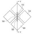
도 3은 도 1에 따른 표시 장치의 접촉 감지층을 도시한 평면도이고, 도 4는 도 3에 도시한 접촉 감지층의 일부의 확대도이고, 도 5는 도 4의 절단선 V-V 선을 따라 잘라 도시한 단면도이다.3 is a plan view illustrating a touch sensing layer of the display device according to FIG. 1 , FIG. 4 is an enlarged view of a portion of the touch sensing layer shown in FIG. 3 , and FIG. It is a cross-sectional view shown.
도 3을 참고하면, 앞서 설명한 바와 같이, 제2 기판(310)의 내면에 접촉 감지층(500)이 배치되어 있다. 접촉 감지층(500)은 터치를 감지할 수 있는 터치 활성 영역(touch active area)(TA) 내에 배치되어 있다. 터치 활성 영역(TA)은 표시 영역(DA)의 전체이거나, 주변 영역(PA)의 일부도 터치 활성 영역(TA)으로 이용될 수 있다. 또한, 표시 영역(DA)의 일부만이 터치 활성 영역(TA)을 이룰 수도 있다.Referring to FIG. 3 , as described above, the
접촉 감지층(500)은 다양한 방식으로 접촉을 감지할 수 있다. 예를 들어, 접촉 감지는 저항막 방식(resistive type), 정전 용량 방식(capacitive type), 전자기 유도형(electro-magnetic type, EM), 광 감지 방식(optical type) 등 다양한 방식으로 분류될 수 있다.The
본 실시예에서는 정전 용량 방식의 접촉 감지를 예로 들어 설명한다.In this embodiment, capacitive touch sensing will be described as an example.
본 실시예에 따른 접촉 감지층(500)은 복수의 터치 전극을 포함하며, 복수의 터치 전극은 복수의 제1 터치 전극(510) 및 복수의 제2 터치 전극(520)을 포함한다. 제1 터치 전극(510)과 제2 터치 전극(520)은 서로 분리되어 있다.The
복수의 제1 터치 전극(510) 및 복수의 제2 터치 전극(520)은 터치 활성 영역(TA)에서 서로 중첩되지 않도록 교호적으로 분산되어 배치되어 있다. 복수의 제1 터치 전극(510)은 열 방향 및 행 방향을 따라 각각 복수 개씩 배치되고, 복수의 제2 터치 전극(520)도 열 방향 및 행 방향을 따라 각각 복수 개씩 배치되어 있다.The plurality of
제1 터치 전극(510)과 제2 터치 전극(520)은 서로 동일한 층에 배치되어 있다. 이에 한정하지 않고, 제1 터치 전극(510)과 제2 터치 전극(520)은 설도 다른 층에 배치되어 있을 수도 있다.The
제1 터치 전극(510)과 제2 터치 전극(520) 각각은 사각형 형상일 수 있으나, 이에 한정되는 것은 아니고 접촉 감지층(500)의 감도 향상을 위해 돌출부를 가지는 등 다양한 형태를 가질 수 있다.Each of the
동일한 행 또는 열에 배열된 복수의 제1 터치 전극(510)은 터치 활성 영역(TA) 내부 또는 외부에서 서로 연결되어 있을 수도 있고 분리되어 있을 수도 있다. 마찬가지로 동일한 열 또는 행에 배열된 복수의 제2 터치 전극(520)의 적어도 일부는 터치 활성 영역(TA) 내부 또는 외부에서 서로 연결되어 있을 수도 있고 분리되어 있을 수도 있다. 예를 들어 도 3에 도시한 바와 같이 동일한 행에 배치된 복수의 제1 터치 전극(510)이 터치 활성 영역(TA) 내부에서 서로 연결되어 있는 경우 동일한 열에 배치된 복수의 제2 터치 전극(520)이 터치 활성 영역(TA) 내부에서 서로 연결되어 있을 수 있다. 더 구체적으로, 각 행에 위치하는 복수의 제1 터치 전극(510)은 제1 연결부(512)를 통해 서로 연결되어 있고, 각 열에 위치하는 복수의 제2 터치 전극(520)은 제2 연결부(522)를 통해 서로 연결되어 있을 수 있다.The plurality of
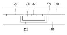
도 4 및 도 5를 참조하면, 서로 이웃한 제1 터치 전극(510) 사이를 연결하는 제1 연결부(512)는 제1 터치 전극(510)과 동일한 층에 배치되어 있다. 또한, 제1 연결부(512)는 제1 터치 전극(510)과 동일한 물질로 형성될 수 있다. 즉, 제1 터치 전극(510)과 제1 연결부(512)는 서로 일체화되어 있을 수 있으며 동시에 패터닝될 수 있다.4 and 5 , the
서로 이웃한 제2 터치 전극(520) 사이를 연결하는 제2 연결부(522)는 제2 터치 전극(520)과 다른 층에 배치되어 있다. 즉, 제2 터치 전극(520)과 제1 연결부(512)는 서로 분리되어 있을 수 있으며 별도로 패터닝될 수 있다. 제2 터치 전극(520)과 제2 연결부(522)는 직접적인 접촉을 통해 서로 연결되어 있다.The
제1 연결부(512)와 제2 연결부(522) 사이에는 제1 절연막(530)이 위치하여 제1 연결부(512)와 제2 연결부(522)를 서로 절연시킨다. 제1 절연막(530)은 도 4 및 도 5에 도시한 바와 같이 제1 연결부(512)와 제2 연결부(522)의 교차부마다 배치된 복수의 독립된 섬형의 절연체일 수 있다. 제1 절연막(530)은 제2 연결부(522)가 제2 터치 전극(520)과 연결될 수 있도록 제2 터치 전극(520)의 적어도 일부를 드러낼 수 있다.A first insulating
이러한 제1 절연막(530)은 그 가장자리가 둥글려진 형태를 가질 수도 있고, 다각형일 수도 있으며, SiOx, SiNx 또는 SiOxNy으로 형성될 수 있다.The first insulating
제1 터치 전극(510), 제2 터치 전극(520) 및 제2 연결부(522) 위에는 제2 절연막(540)이 배치되어 있다. 제2 절연막(540)은 터치 활성 영역(TA)의 전반에 걸쳐 배치되어 있으며, SiOx, SiNx 또는 SiOxNy으로 형성될 수 있다.A second insulating
도 4 및 도 5에 도시한 바와 달리, 서로 이웃한 제2 터치 전극(520) 사이를 연결하는 제2 연결부(522)가 제1 터치 전극(510)과 동일한 층에 위치하며 제1 터치 전극(510)과 일체화되어 있고, 서로 이웃한 제1 터치 전극(510) 사이를 연결하는 제1 연결부(512)는 제1 터치 전극(510)과 다른 층에 위치할 수도 있다.4 and 5 , the
다시 도 3을 참고하면, 각 행의 서로 연결된 제1 터치 전극(510)은 제1 터치 배선(511)을 통해 터치 센서 제어부(도시하지 않음)와 연결되고, 각 열의 서로 연결된 제2 터치 전극(520)은 제2 터치 배선(521)을 통해 터치 센서 제어부(도시하지 않음)와 연결된다. 제1 터치 배선(511)과 제2 터치 배선(521)은 도 3에 도시한 바와 같이 주변 영역(PA)에 위치할 수 있으나, 이와 달리 터치 활성 영역(TA)에 위치할 수도 있다.Referring back to FIG. 3 , the
제1 터치 배선(511)과 제2 터치 배선(521)의 끝부분은 제2 기판(310)의 주변 영역(PA)에서 패드부(560)를 형성한다.Ends of the
제1 터치 전극(510) 및 제2 터치 전극(520)은 박막 표시층(200)으로부터 빛이 투과될 수 있도록 소정의 투과도 이상을 가진다. 예를 들어, 제1 터치 전극(510) 및 제2 터치 전극(520)은 ITO(indium tin oxide), IZO(indium zinc oxide), 은 나노 와이어(AgNw) 등의 얇은 금속층, 메탈 메쉬(metal mesh), 탄소 나노 튜브(CNT) 등의 투명한 도전 물질로 만들어질 수 있으나 이에 한정되는 것은 아니다.The
제1 터치 배선(511)과 제2 터치 배선(521)은 제1 터치 전극(510) 및 제2 터치 전극(520)이 포함하는 투명한 도전 물질 또는 몰리브덴(Mo), 은(Ag), 티타늄(Ti), 구리(Cu), 알루미늄(Ti), 몰리브덴/알루미늄/몰리브덴(Mo/Al/Mo) 등의 저저항 물질을 포함할 수 있다.The
서로 이웃하는 제1 터치 전극(510)과 제2 터치 전극(520)은 접촉 감지 센서로서 기능하는 상호 감지 축전기(mutual sensing capacitor)를 형성한다. 상호 감지 축전기는 제1 터치 전극(510) 및 제2 터치 전극(520) 중 하나를 통해 감지 입력 신호를 입력 받고 외부 물체의 접촉에 의한 전하량 변화를 감지 출력 신호로서 나머지 터치 전극을 통해 출력할 수 있다.The first and
도 3 내지 도 5에 도시한 바와 달리, 복수의 제1 터치 전극(510)과 복수의 제2 터치 전극(520)은 서로 분리되어 각각 터치 배선(도시하지 않음)을 통해 터치 센세 제어부와 연결될 수도 있다. 이 경우 각 터치 전극은 접촉 감지 센서로서 자가 감지 축전기(self sensing capacitance)를 형성할 수 있다. 자가 감지 축전기는 감지 입력 신호를 입력 받아 소정 전하량으로 충전될 수 있고, 손가락 등의 외부 물체의 접촉이 있으면 충전 전하량에 변화가 생겨 입력된 감지 입력 신호와 다른 감지 출력 신호를 출력할 수 있다.3 to 5 , the plurality of
그러면, 도 6 및 도 7을 참고하여 본 실시예에 따른 박막 표시층에 대해 상세하게 설명한다.Then, the thin film display layer according to the present embodiment will be described in detail with reference to FIGS. 6 and 7 .
앞서 설명한 바와 같이, 박막 표시층(200)은 복수의 화소를 포함한다.As described above, the thin
도 6은 본 발명의 일 실시예에 따른 표시 장치의 하나의 화소의 배치도이고, 도 7은 도 6의 절단선 Ⅶ-Ⅶ선을 따라 잘라 도시한 단면도이다.6 is a layout view of one pixel of a display device according to an exemplary embodiment, and FIG. 7 is a cross-sectional view taken along the cutting line VII-VII of FIG. 6 .
도 6 및 도 7을 참고하면, 박막 표시층(200)은 버퍼층(120), 스위칭 및 구동 반도체층(154a, 154b), 게이트 절연막(140), 게이트선(121), 제1 스토리지 축전판(128), 층간 절연막(160), 데이터선(171), 구동 전압선(172), 스위칭 드레인 전극(175a), 구동 드레인 전극(175b) 및 보호막(180)을 포함한다.6 and 7 , the thin
버퍼층(120)은 제1 기판(110) 위에 배치되어 있으며, 질화규소(SiNx)의 단일막 또는 질화 규소(SiNx)와 산화 규소(SiO2)가 적층된 이중막 구조로 형성될 수 있다. 버퍼층(120)은 불순물 또는 수분과 같이 불필요한 성분의 침투를 방지하면서 동시에 표면을 평탄화하는 역할을 한다.The
버퍼층(120) 위에는 스위칭 반도체층(154a) 및 구동 반도체층(154b)이 서로 이격되어 배치되어 있다. 스위칭 반도체층(154a) 및 구동 반도체층(154b)은 다결정 실리콘으로 이루어져 있으며, 채널 영역(1545a, 1545b)과, 소스 영역(1546a, 1546b) 및 드레인 영역(1547a, 1547b)을 포함한다. 소스 영역(1546a, 1546b) 및 드레인 영역(1547a, 1547b)은 각각 채널 영역(1545a, 1545b)의 양 옆에 배치되어 있다.A switching
채널 영역(1545a, 1545b)은 불순물이 도핑되지 않은 폴리 실리콘, 즉 진성 반도체(intrinsic semiconductor)이고, 소스 영역(1546a, 1546b) 및 드레인 영역(1547a, 1547b)은 도전성 불순물이 도핑된 폴리 실리콘, 즉 불순물 반도체(impurity semiconductor)이다.The
스위칭 반도체층(154a) 및 구동 반도체층(154b)의 채널 영역(1545a, 1545b) 위에는 게이트 절연막(140)이 배치되어 있다. 게이트 절연막(140)은 질화 규소 및 산화 규소 중 적어도 하나를 포함한 단층 또는 복수층일 수 있다.A
게이트 절연막(140) 위에는 게이트선(121)이 배치되어 있고, 버퍼층(120) 위에는 제1 스토리지 축전판(128)이 배치되어 있다.A
게이트선(121)은 가로 방향으로 길게 뻗어 게이트 신호를 전달하며, 게이트선(121)으로부터 스위칭 반도체층(154a)으로 돌출한 스위칭 게이트 전극(124a)을 포함한다. 게이트선(121)은 제1 게이트 구동 회로(410) 및 제2 게이트 구동 회로(420)에 연결되어 있다.The
제1 스토리지 축전판(128)은 제1 스토리지 축전판(128)으로부터 구동 반도체층(154b)으로 돌출되어 있는 구동 게이트 전극(124b)을 포함한다. 스위칭 게이트 전극(124a) 및 구동 게이트 전극(124b)은 각각 채널 영역(1545a, 1545b)과 중첩한다.The first
게이트선(121), 제1 스토리지 축전판(128) 및 버퍼층(120) 위에는 층간 절연막(160)이 배치되어 있다.An interlayer insulating
층간 절연막(160)에는 스위칭 반도체층(154a)의 소스 영역(1546a)과 드레인 영역(1547a)을 각각 노출하는 스위칭 소스 접촉 구멍(61a)와 스위칭 드레인 접촉 구멍(62a)이 형성되어 있다. 또한, 층간 절연막(160)에는 구동 반도체층(154b) 소스 영역(1546b)과 드레인 영역(1547b)을 각각 노출하는 구동 소스 접촉 구멍(61b)와 구동 드레인 접촉 구멍(62b)이 형성되어 있다.A switching
층간 절연막(160) 위에는 데이터선(171), 구동 전압선(172), 스위칭 드레인 전극(175a) 및 구동 드레인 전극(175b)이 배치되어 있다.A
데이터선(171)은 데이터 신호를 전달하며 게이트선(121)과 교차하는 방향으로 뻗어 있고, 데이터선(171)으로부터 스위칭 반도체층(154a)을 향해서 돌출되어 있는 스위칭 소스 전극(173a)을 포함한다.The
구동 전압선(172)은 구동 전압을 전달하며 데이터선(171)과 분리되어있으며, 데이터선(171)과 동일한 방향으로 뻗어 있다. 구동 전압선(172)은 구동 전압선(172)으로부터 구동 반도체층(154b)을 향해서 돌출되어 있는 구동 소스 전극(173b) 및 구동 전압선(172)에서 돌출하여 제1 스토리지 축전판(128)과 중첩하고 있는 제2 스토리지 축전판(178)을 포함한다. 여기서, 제1 스토리지 축전판(128)과 제2 스토리지 축전판(178)은 층간 절연막(160)을 유전체로 하여 스토리지 커패시터(Cst)를 이룬다.The driving
스위칭 드레인 전극(175a)은 스위칭 소스 전극(173a)과 마주하고 구동 드레인 전극(175b)은 구동 소스 전극(173b)과 마주한다.The switching
스위칭 소스 전극(173a)과 스위칭 드레인 전극(175a)은 각각 스위칭 소스 접촉 구멍(61a)와 스위칭 드레인 접촉 구멍(62a)을 통하여, 스위칭 반도체층(154a)의 소스 영역(1546a)과 드레인 영역(1547a)에 연결되어 있다. 또한, 스위칭 드레인 전극(175a)은 연장되어 층간 절연막(160)에 형성되어 있는 제1 접촉 구멍(63)을 통해서 제1 스토리지 축전판(128) 및 구동 게이트 전극(124b)과 전기적으로 연결되어 있다.The switching
구동 소스 전극(173b)과 구동 드레인 전극(175b)은 각각 구동 소스 접촉 구멍(61b)와 구동 드레인 접촉 구멍(62b)을 통하여, 구동 반도체층(154b)의 소스 영역(1546b)과 드레인 영역(1547b)에 연결되어 있다.The driving
스위칭 반도체층(154a), 스위칭 게이트 전극(124a), 스위칭 소스 전극(173a) 및 스위칭 드레인 전극(175a)은 스위칭 박막 트랜지스터(T1)를 이루고, 구동 반도체층(154b), 구동 게이트 전극(124b), 구동 소스 전극(173b) 및 구동 드레인 전극(175b)은 구동 박막 트랜지스터(T2)를 이룬다.The switching
데이터선(171), 구동 전압선(172), 스위칭 드레인 전극(175a) 및 구동 드레인 전극(175b) 위에는 보호막(180)이 형성되어 있다.A
보호막(180)에는 구동 드레인 전극(175b)를 노출하는 제2 접촉 구멍(185)이 형성되어 있다.A
보호막(180) 위에는 유기 발광 다이오드(70) 및 화소 정의막(350)이 배치되어 있다.An organic
유기 발광 다이오드(70)는 화소 전극(191), 유기 발광층(360) 및 공통 전극(270)을 포함한다.The organic
화소 전극(191)은 보호막(180) 위에 배치되어 있고, 층간 절연막(160)에 형성된 제2 접촉 구멍(185)을 통해서 구동 박막 트랜지스터(T2)의 구동 드레인 전극(175b)과 전기적으로 연결되어 있다. 이러한 화소 전극(191)은 유기 발광 다이오드(70)의 애노드(anode) 전극이 된다.The
화소 전극(191)은 ITO(Indium Tin Oxide), IZO(Indium Zinc Oxide), ZnO(산화 아연) 또는 In2O3(Indium Oxide) 등의 투명한 도전 물질이나 리튬(Li), 칼슘(Ca), 플루오르화리튬/칼슘(LiF/Ca), 플루오르화리튬/알루미늄(LiF/Al), 알루미늄(Al), 은(Ag), 마그네슘(Mg), 또는 금(Au) 등의 반사성 금속으로 이루어질 수 있다.The
화소 정의막(350)은 화소 전극(191)의 가장자리부 및 보호막(180) 위에 배치되어 있다.The
화소 정의막(350)은 화소 전극(191)을 노출하는 개구부를 가진다. 화소 정의막(350)은 폴리아크릴계(polyacrylates) 또는 폴리이미드계(polyimides) 등의 수지로 이루어질 수 있다.The
화소 정의막(350)의 개구부 내의 화소 전극(191) 위에는 유기 발광층(360)이 배치되어 있다. 유기 발광층(360)은 발광층, 정공 수송층(hole-injection layer, HIL), 정공 수송층(hole-transporting layer, HTL), 전자 수송층(electron-transporting layer, ETL) 및 전자 주입층(electron-injection layer, EIL) 중 하나 이상을 포함하는 복수층으로 이루어져 있다. 유기 발광층(360)이 이들 모두를 포함할 경우 정공 주입층이 애노드 전극인 화소 전극(191) 위에 위치하고 그 위로 정공 수송층, 발광층, 전자 수송층, 전자 주입층이 차례로 적층될 수 있다.An
유기 발광층(360)은 적색을 발광하는 적색 유기 발광층, 녹색을 발광하는 녹색 유기 발광층 및 청색을 발광하는 청색 유기 발광층을 포함할 수 있으며, 적색 유기 발광층, 녹색 유기 발광층 및 청색 유기 발광층은 각각 적색 화소, 녹색 화소 및 청색 화소에 형성되어 컬러 화상을 구현하게 된다.The
또한, 유기 발광층(360)은 적색 유기 발광층, 녹색 유기 발광층 및 청색 유기 발광층을 적색 화소, 녹색 화소 및 청색 화소에 모두 함께 적층하고, 각 화소별로 적색 색필터, 녹색 색필터 및 청색 색필터를 형성하여 컬러 화상을 구현할 수 있다. 다른 예로, 백색을 발광하는 백색 유기 발광층을 적색 화소, 녹색 화소 및 청색 화소 모두에 형성하고, 각 화소별로 각각 적색 색필터, 녹색 색필터 및 청색 색필터를 형성하여 컬러 화상을 구현할 수도 있다. 백색 유기 발광층과 색필터를 이용하여 컬러 화상을 구현하는 경우, 적색 유기 발광층, 녹색 유기 발광층 및 청색 유기 발광층을 각각의 개별 화소 즉, 적색 화소, 녹색 화소 및 청색 화소에 증착하기 위한 증착 마스크를 사용하지 않아도 된다.In addition, in the organic
다른 예에서 설명한 백색 유기 발광층은 하나의 유기 발광층으로 형성될 수 있음은 물론이고, 복수 개의 유기 발광층을 적층하여 백색을 발광할 수 있도록 한 구성까지 포함한다. 예로, 적어도 하나의 옐로우 유기 발광층과 적어도 하나의 청색 유기 발광층을 조합하여 백색 발광을 가능하게 한 구성, 적어도 하나의 시안 유기 발광층과 적어도 하나의 적색 유기 발광층을 조합하여 백색 발광을 가능하게 한 구성, 적어도 하나의 마젠타 유기 발광층과 적어도 하나의 녹색 유기 발광층을 조합하여 백색 발광을 가능하게 한 구성 등도 포함할 수 있다.The white organic light emitting layer described in another example may be formed as one organic light emitting layer, and includes a configuration in which a plurality of organic light emitting layers are stacked to emit white light. For example, a configuration that enables white light emission by combining at least one yellow organic light emitting layer and at least one blue organic light emitting layer, a configuration that enables white light emission by combining at least one cyan organic light emitting layer and at least one red organic light emitting layer, A configuration in which at least one magenta organic emission layer and at least one green organic emission layer are combined to enable white light emission may be included.
공통 전극(270)은 화소 정의막(350) 및 유기 발광층(360) 위에 배치되어 있다. 공통 전극(270)은 ITO, IZO, ZnO 또는 In2O3 등의 투명한 도전 물질이나 리튬, 칼슘, 플루오르화리튬/칼슘, 플루오르화리튬/알루미늄), 알루미늄, 은, 마그네슘, 또는 금 등의 반사성 금속으로 이루어질 수 있다. 이러한 공통 전극(270)은 유기 발광 다이오드(70)의 캐소드(cathode) 전극이 된다.The
한편, 접촉 감지층(500)은 다른 형상으로 형성될 수 있다. 이에, 도 8을 참고하여 본 발명의 다른 실시예에 따른 접촉 감지층(500)에 대해 설명한다.Meanwhile, the
도 8은 본 발명의 다른 실시예에 따른 접촉 감지층을 도시한 평면도이다.8 is a plan view illustrating a touch sensing layer according to another embodiment of the present invention.
도 8을 참고하면, 제2 기판(310)의 내면에 접촉 감지층(500)이 배치되어 있다. 접촉 감지층(500)은 터치를 감지할 수 있는 터치 활성 영역(touch active area)(TA) 내에 배치되어 있다.Referring to FIG. 8 , a
본 실시예에 따른 접촉 감지층(500)은 복수의 터치 전극을 포함하며, 복수의 터치 전극은 복수의 제1 터치 전극(510) 및 복수의 제2 터치 전극(520)을 포함한다. 제1 터치 전극(510)과 제2 터치 전극(520)은 서로 분리되어 있다.The
복수의 제1 터치 전극(510) 및 복수의 제2 터치 전극(520)은 터치 활성 영역(TA)에서 서로 중첩되지 않도록 교호적으로 분산되어 배치되어 있다. 복수의 제1 터치 전극(510)은 행 방향을 따라 각각 복수 개씩 배치되고, 복수의 제2 터치 전극(520)도 행 방향을 따라 각각 복수 개씩 배치되어 있다.The plurality of
제1 터치 전극(510) 및 제2 터치 전극(520) 각각은 삼각형 형상이고, 제1 터치 전극(510)은 제1 터치 연결부(540)를 통하여 연결되어 있고, 제2 터치 전극(520)은 제2 터치 연결부(550)를 통하여 연결되어 있다.Each of the
제1 터치 연결부(540)는 행 방향으로 배치되어 있으며, 복수 개의 제1 터치 전극(510) 중 일부를 연결하고, 제2 터치 연결부(550)는 행 방향으로 배치되어 있으며, 복수 개의 제2 터치 전극(520) 중 일부를 연결한다.The first
제1 터치 전극(510) 및 제2 터치 전극(520)은 동일한 층에 형성될 수 있으며, 제1 터치 전극(510) 및 제2 터치 전극(520)을 절연시키기 위한 절연막이 형성될 수 있다.The
제1 터치 연결부(540)에 의해 연결된 제1 터치 전극(510)은 제1 터치 배선(511)을 통하여 터치 센서 제어부(도시하지 않음)와 연결되고, 터치 전극(520)은 제2 터치 배선(521)을 통해 터치 센서 제어부(도시하지 않음)와 연결된다.The
제1 터치 배선(511)과 제2 터치 배선(521)은 도 3에 도시한 바와 같이 주변 영역(PA)에 위치할 수 있으나, 이와 달리 터치 활성 영역(TA)에 위치할 수도 있다.The
제1 터치 배선(511)과 제2 터치 배선(521)의 끝부분은 제2 기판(310)의 주변 영역(PA)에서 패드부(560)를 형성한다.Ends of the
이상의 도 3 및 도 8에 따른 접촉 감지층은 정전 용량 방식의 접촉 감지를 설명하였지만, 앞서 언급한 바와 같이, 이에 한정하지 않고, 저항막 방식(resistive type), 정전 용량 방식(capacitive type), 전자기 유도형(electro-magnetic type, EM), 광 감지 방식(optical type) 등 다양한 방식의 접촉 감지층이 배치되어 있을 수 있다.The touch sensing layer according to FIGS. 3 and 8 described the capacitive type touch sensing, but as mentioned above, it is not limited thereto, and the resistive type, capacitive type, electromagnetic Various types of contact sensing layers such as an electro-magnetic type (EM) or an optical type may be disposed.
이하에서는 도 9 내지 도 11을 참고하여, 본 발명의 다른 실시예에 따른 표시 장치에 대해 설명한다.Hereinafter, a display device according to another exemplary embodiment of the present invention will be described with reference to FIGS. 9 to 11 .
도 9는 본 발명의 다른 실시예에 따른 표시 장치의 단면도이다.9 is a cross-sectional view of a display device according to another exemplary embodiment.
도 9를 참고하면, 본 실시예에 따른 표시 장치는 제1 패널(100), 제1 패널(100)에 대향하는 제2 패널(300) 및 제1 패널(100)과 제2 패널(300) 사이에 개재되어 있는 액정층(600)을 포함한다.Referring to FIG. 9 , the display device according to the present exemplary embodiment includes a
제1 패널(100)과 제2 패널(300)은 밀봉재 (330)에 의해 서로 합착되어 있다. 밀봉재(330)는 주변 영역(PA)에 배치되어 있다.The
주변 영역(PA)에는 제1 게이트 구동 회로(410) 및 제2 게이트 구동 회로(420)가 배치되어 있다. 제1 게이트 구동 회로(410) 및 제2 게이트 구동 회로(420)는 표시 영역(DA)에 게이트 구동 신호를 인가하며, 표시 영역(DA)의 좌측 및 우측에 각각 배치되어 있다.A first
제1 게이트 구동 회로(410) 및 제2 게이트 구동 회로(420)는 그 일부가 밀봉재(330)와 중첩하여 배치되어 있다.A portion of the first
제1 패널(100)은 유리 또는 플라스틱 등의 투명한 절연 물질로 이루어진 제1 기판(110) 및 박막 표시층(200)을 포함한다. 박막 표시층(200)은 표시 영역(DA)에 배치되어 있으며, 제1 기판(110)의 내면 즉, 제1 기판(110)의 양면 중, 제2 패널(300)과 마주하는 면에 배치되어 있다.The
박막 표시층(200)은 복수의 화소를 포함한다. 각 화소는 후술하는 박막 트랜지스터 및 액정층(600)에 전계를 인가하는 화소 전극(191)과 공통 전극(270)을 포함한다.The thin
또한, 제1 패널(100)은 주변 영역(PA)에 배치되어 있는 제3 하부 게이트 구동 회로(415), 제4 하부 게이트 구동 회로(425), 제3 하부 게이트 구동 회로(415)에 연결되어 있는 제1 하부 접촉부(413) 및 제4 하부 게이트 구동 회로(425)에 연결되어 있는 제2 하부 접촉부(423)를 포함한다.Also, the
제1 하부 접촉부(413) 및 제2 하부 접촉부(423)는 도전성 물질로 이루어져 있다.The first
제3 하부 게이트 구동 회로(415), 제4 하부 게이트 구동 회로(425), 제1 하부 접촉부(413) 및 제2 하부 접촉부(423)는 제1 기판(110)의 내면 즉, 제1 기판(110)의 양면 중, 제2 패널(300)과 마주하는 면에 배치되어 있다.The third lower
제1 하부 게이트 구동 회로(411) 및 제2 하부 게이트 구동 회로(421)는 각 화소에 연결되어 있다.The first lower
제2 패널(300)은 유리 또는 플라스틱 등의 투명한 절연 물질로 이루어진 제2 기판(310) 및 접촉 감지층(500)을 포함한다. 접촉 감지층(500)은 제2 기판(310)의 내면 즉, 제2 기판(310)의 양면 중 제1 패널(100)과 마주하는 면에 배치되어 있다. 이에, 접촉 감지층(500)은 박막 표시층(200)과 마주하고 있다. 또한, 제2 기판(310)의 외면을 식각하여 제2 기판(310)의 두께를 감소시킬 수 있다.The
본 실시예에 따른 접촉 감지층(500)은 도 1의 실시예에 따른 표시 장치의 접촉 감지층과 동일하다. 이에, 본 실시예에 따른 접촉 감지층(500)의 설명은 생략한다.The
또한, 제2 패널(300)은 주변 영역(PA)에 배치되어 있는 제3 상부 게이트 구동 회로(416), 제4 상부 게이트 구동 회로(426), 제3 상부 게이트 구동 회로(416)에 연결되어 있는 제1 상부 접촉부(414) 및 제4 상부 게이트 구동 회로(426)에 연결되어 있는 제2 상부 접촉부(424)를 포함한다.In addition, the
제1 상부 접촉부(414) 및 제2 상부 접촉부(424)는 도전성 물질로 이루어져 있다.The first
제3 상부 게이트 구동 회로(416), 제4 상부 게이트 구동 회로(426), 제1 상부 접촉부(414) 및 제2 상부 접촉부(424)는 제2 기판(310)의 내면 즉, 제2 기판(310)의 양면 중 제1 패널(100)과 마주하는 면에 배치되어 있다.The third upper
제3 하부 게이트 구동 회로(415)와 제3 상부 게이트 구동 회로(416)가 서로 마주하고 있고, 제4 하부 게이트 구동 회로(425)와 제4 상부 게이트 구동 회로(426)가 서로 마주하고 있다. 또한, 제1 하부 접촉부(413)와 제1 상부 접촉부(414)가 서로 마주하고 있고, 제2 하부 접촉부(423)와 제2 상부 접촉부(424)가 서로 마주하고 있다.The third lower
밀봉재(330)는 제1 패널(100)과 제2 패널(300)을 합착하는데, 제1 하부 게이트 구동 회로(411) 및 제1 상부 게이트 구동 회로(412)와 일부 중첩하고, 제2 하부 게이트 구동 회로(421) 및 제2 상부 게이트 구동 회로(422)와 일부 중첩한다.The sealing
밀봉재(330)의 내부에는 도전성 물질로 이루어진 복수 개의 도전볼(335)이 배치되어 있다. 복수 개의 도전볼(335)들은 서로 접촉되어 있다.A plurality of
또한, 도전볼(335)은 밀봉재(330)가 제3 하부 게이트 구동 회로(415) 및 제3 상부 게이트 구동 회로(416)와 중첩하는 부분에서 제1 하부 접촉부(413) 및 제1 상부 접촉부(414)에 접촉되어 있다. 이에, 제1 하부 접촉부(413) 및 제1 상부 접촉부(414)는 도전볼(335)에 의해 전기적으로 연결되어 있다. 따라서, 제3 하부 게이트 구동 회로(415)와 제3 상부 게이트 구동 회로(416)는 전기적으로 연결된다. 이러한 제3 하부 게이트 구동 회로(415)와 제3 상부 게이트 구동 회로(416)는 제1 게이트 구동 회로(410)를 이룬다.In addition, the
또한, 도전볼(335)은 밀봉재(330)가 제4 하부 게이트 구동 회로(425) 및 제4 상부 게이트 구동 회로(426)와 중첩하는 부분에서 제2 하부 접촉부(423) 및 제2 상부 접촉부(424)에 접촉되어 있다. 이에, 제2 하부 접촉부(423) 및 제2 상부 접촉부(424)는 도전볼(335)에 의해 전기적으로 연결되어 있다. 따라서, 제4 하부 게이트 구동 회로(425)와 제2 상부 게이트 구동 회로(426)는 전기적으로 연결된다. 이러한 제4 하부 게이트 구동 회로(425)와 제4 상부 게이트 구동 회로(426)는 제2 게이트 구동 회로(420)를 이룬다.In addition, the
제1 게이트 구동 회로(410) 및 제2 게이트 구동 회로(410)는 각각 표시 영역(DA)에 게이트 신호를 인가하는데, 제3 하부 게이트 구동 회로(415) 및 제4 하부 게이트 구동 회로(425)는 각각 복수 개의 박막 트랜지스터를 포함하고, 제3 상부 게이트 구동 회로(416) 및 제4 상부 게이트 구동 회로(426)는 각각 복수 개의 커패시터를 포함한다.The first
그러면, 도 10 및 도 11을 참고하여 본 실시예에 따른 박막 표시층에 대해 설명한다.Then, the thin film display layer according to the present embodiment will be described with reference to FIGS. 10 and 11 .
앞서 설명한 바와 같이, 박막 표시층(200)은 복수의 화소를 포함한다.As described above, the thin
도 10은 본 발명의 다른 실시예에 따른 표시 장치의 하나의 화소의 배치도이고, 도 11은 도 10의 절단선 ⅩⅠ-ⅩⅠ 선을 따라 잘라 도시한 단면도이다.FIG. 10 is a layout view of one pixel of a display device according to another exemplary embodiment of the present invention, and FIG. 11 is a cross-sectional view taken along the line XII-XI of FIG. 10 .
도 10 및 도 11을 참고하면, 본 실시예에 따른 박막 표시층(200)은 게이트선(121), 유지 전극선(131), 게이트 절연막(140), 반도체층(151), 선형 및 섬형 저항성 접촉 부재(ohmic contact)(161, 165), 데이터선(171), 드레인 전극(175), 화소 전극(191), 보호막(180) 및 공통 전극(270)을 포함한다.10 and 11 , the thin
게이트선(121)은 게이트 신호를 전달하며 주로 가로 방향으로 뻗어 있다. 게이트선(121)은 위로 돌출한 복수의 게이트 전극(124)을 포함한다. 게이트선(121)은 제1 게이트 구동 회로(410) 및 제2 게이트 구동 회로(420)에 연결되어 있다.The
유지 전극선(131)은 기준 전압(reference voltage)를 인가 받으며, 게이트선(121)과 거의 나란하게 뻗어 있으며, 유지 전극선(131)은 아래로 돌출한 복수의 돌출부(135)를 포함한다.The
게이트선(121) 및 유지 전극선(131) 위에는 질화규소(SiNx) 또는 산화규소(SiOx) 등으로 이루어지는 게이트 절연막(140)이 배치되어 있다. 게이트 절연막(140)은 물리적 성질이 다른 적어도 두 개의 절연층을 포함하는 다층막 구조를 가질 수도 있다.A
게이트 절연막(140) 위에는 수소화 비정질 규소(hydrogenated amorphous silicon)(비정질 규소는 약칭 a-Si로 씀) 또는 다결정 규소(polysilicon) 등으로 만들어진 반도체층(151)이 배치되어 있다. 반도체층(151)은 주로 세로 방향으로 뻗어 있으며, 반도체층(151)은 게이트 전극(124)을 향하여 뻗어 나온 돌출부(154)를 포함한다.A
반도체층(151) 위에는 선형 및 섬형 저항성 접촉 부재(ohmic contact)(161, 165)가 배치되어 있다. 저항성 접촉 부재(161, 165)는 인 따위의 n형 불순물이 고농도로 도핑되어 있는 n+ 수소화 비정질 규소 따위의 물질로 만들어지거나 실리사이드(silicide)로 만들어질 수 있다. 각 선형 저항성 접촉 부재(161)는 돌출부(163)를 가지고 있으며, 이 돌출부(163)와 섬형 저항성 접촉 부재(165)는 쌍을 이루어 반도체층(151)의 돌출부(154) 위에 배치되어 있다.Linear and island-shaped
저항성 접촉 부재(161, 165) 위에는 데이터선(171)과 드레인 전극(175)이 배치되어 있다.A
데이터선(171)은 데이터 신호를 전달하며 주로 세로 방향으로 뻗어 게이트선(121)과 교차한다. 데이터선(171)은 게이트 전극(124)을 향하여 뻗은 소스 전극(173)을 포함한다.The
드레인 전극(175)은 데이터선(171)과 분리되어 있고 게이트 전극(124)을 중심으로 소스 전극(173)과 마주한다. 드레인 전극(175)은 막대형인 한 쪽 끝 부분과 면적이 넓은 확장부를 포함한다. 막대형 끝 부분은 구부러진 소스 전극(173)으로 일부 둘러싸여 있다.The
게이트 전극(124), 소스 전극(173) 및 드레인 전극(175)은 반도체층(151)의 돌출부(154)와 함께 하나의 박막 트랜지스터(thin film transistor, TFT)를 이루며, 박막 트랜지스터의 채널(channel)은 소스 전극(173)과 드레인 전극(175) 사이의 반도체층(151)의 돌출부(154)에 형성된다.The
저항성 접촉 부재(161, 165)는 그 아래의 반도체층(151)과 그 위의 데이터선(171) 및 드레인 전극(175) 사이에 존재하며 이들 사이의 접촉 저항을 낮추어 준다.The
드레인 전극(175) 및 게이트 절연막(140) 위에는 화소 전극(191)이 배치되어 있다.A
화소 전극(191)은 화소 영역을 덮고 있는 판 형태(plane shape)를 가지고, 드레인 전극(175)의 확장부와 직접 접촉하여 드레인 전극(175)으로부터 데이터 전압을 인가 받는다.The
화소 전극(191)은 ITO(indium tin oxide) 또는 IZO(indium zinc oxide) 등의 투명한 도전 물질로 이루어져 있다.The
소스 전극(173), 드레인 전극(175), 노출된 반도체층(151)의 돌출부(154) 부분 및 화소 전극(191) 위에는 보호막(180)이 배치되어 있다.A
보호막(180)은 무기 절연물 또는 유기 절연물 따위로 만들어지며 표면이 평탄할 수 있다. 무기 절연물의 예로는 질화규소와 산화규소를 들 수 있다. 유기 절연물은 감광성(photosensitivity)을 가질 수 있으며 그 유전 상수(dielectric constant)는 약 4.0 이하인 것이 바람직하다. 그러나 보호막(180)은 유기막의 우수한 절연 특성을 살리면서도 노출된 반도체층(151)의 돌출부(154) 부분에 해가 가지 않도록 하부 무기막과 상부 유기막의 이중막 구조를 가질 수 있다.The
보호막(180) 및 게이트 절연막(140)에는 유지 전극선(131)의 돌출부(135)를 노출하는 제3 접촉 구멍(187)가 형성되어 있다.A
보호막(180) 위에는 공통 전극(270)이 배치되어 있다. 공통 전극(270)은 ITO(indium tin oxide) 또는 IZO(indium zinc oxide) 등의 투명한 도전 물질로 이루어져 있다. 또한, 공통 전극(270)은 알루미늄(Al)이나 알루미늄 합금 등 알루미늄 계열 금속, 은(Ag)이나 은 합금 등 은 계열 금속, 몰리브덴(Mo)이나 몰리브덴 합금 등 몰리브덴 계열 금속, 크롬(Cr), 탄탈륨(Ta) 및 티타늄(Ti) 등의 불투명한 도전 물질로 이루어질 수 있다.A
공통 전극(270)은 제3 접촉 구멍(187)을 통하여 유지 전극선(131)의 돌출부(135)와 연결되어 있으며, 유지 전극선(131)으로부터 기준 전압(reference voltage)을 인가 받는다.The
공통 전극(270)은 복수의 가지 전극(271)을 포함한다. 공통 전극(270)의 가지 전극(271)은 게이트선(121)과 거의 나란한 방향으로 뻗어 있으며, 게이트선(121)과 약 5도 내지 약 20도의 각도를 이루도록 기울어질 수 있다.The
데이터 전압이 인가된 화소 전극(191)은 기준 전압을 인가 받는 공통 전극(270)과 함께 전기장을 생성함으로써, 두 전극(191, 270) 위에 위치하는 액정층(600)의 액정 분자는 전기장의 방향과 평행한 방향으로 회전한다. 이와 같이 결정된 액정 분자의 회전 방향에 따라 액정층(600)을 통과하는 빛의 편광이 달라진다.The
이상에서 본 발명의 바람직한 실시예에 대하여 상세하게 설명하였지만 본 발명의 권리범위는 이에 한정되는 것은 아니고 다음의 청구범위에서 정의하고 있는 본 발명의 기본 개념을 이용한 당업자의 여러 변형 및 개량 형태 또한 본 발명의 권리범위에 속하는 것이다.Although the preferred embodiment of the present invention has been described in detail above, the scope of the present invention is not limited thereto, and various modifications and improvements by those skilled in the art using the basic concept of the present invention defined in the following claims are also present is within the scope of the
100: 제1 패널110: 제1 기판
200: 박막 표시층300: 제2 패널
310: 제2 기판330: 밀봉재
335: 도전볼410: 제1 게이트 구동 회로
420: 제2 게이트 구동 회로500: 접촉 감지층100: first panel 110: first substrate
200: thin film display layer 300: second panel
310: second substrate 330: sealing material
335: conductive ball 410: first gate driving circuit
420: second gate driving circuit 500: touch sensing layer
Claims (15)
Translated fromKorean상기 제1 패널과 마주하는 제2 패널, 그리고
상기 제1 패널 및 상기 제2 패널을 합착하는 밀봉재를 포함하며,
상기 제1 패널은
화상을 표시하는 표시 영역 및 상기 표시 영역의 주변의 주변 영역을 포함하는 제1 기판,
상기 제1 기판의 상기 표시 영역에 위치하는 박막 표시층, 그리고
상기 제1 기판의 상기 주변 영역에 위치하고 상기 박막 표시층의 일측에 위치하는 제1 하부 게이트 구동 회로를 포함하고,
상기 제2 패널은
상기 제1 기판의 상기 표시 영역 및 상기 주변 영역에 각각 대응하는 표시 영역 및 주변 영역을 포함하는 제2 기판,
상기 제2 기판의 상기 표시 영역에 위치하는 접촉 감지층, 그리고
상기 제2 기판의 상기 주변 영역에 위치하고 상기 접촉 감지층의 일측에 위치하는 제1 상부 게이트 구동 회로를 포함하고,
상기 밀봉재는 상기 제1 하부 게이트 구동 회로 및 상기 제1 상부 게이트 구동 회로와 적어도 부분적으로 중첩하고,
상기 밀봉재는 상기 제1 하부 게이트 구동 회로와 상기 제1 상부 게이트 구동 회로를 전기적으로 연결하는 복수의 도전볼을 포함하는 표시 장치.first panel;
a second panel facing the first panel, and
a sealing material bonding the first panel and the second panel;
the first panel
a first substrate including a display area displaying an image and a peripheral area around the display area;
a thin film display layer positioned in the display area of the first substrate; and
a first lower gate driving circuit positioned in the peripheral region of the first substrate and positioned at one side of the thin film display layer;
the second panel
a second substrate including a display area and a peripheral area respectively corresponding to the display area and the peripheral area of the first substrate;
a touch sensing layer positioned in the display area of the second substrate; and
and a first upper gate driving circuit positioned in the peripheral region of the second substrate and positioned at one side of the touch sensing layer;
the sealing material at least partially overlaps the first lower gate driving circuit and the first upper gate driving circuit;
The encapsulant includes a plurality of conductive balls electrically connecting the first lower gate driving circuit and the first upper gate driving circuit.
상기 제1 패널은 상기 제1 하부 게이트 구동 회로에 연결되어 있고 도전성 물질로 이루어져 있는 제1 하부 접촉부를 더 포함하는 표시 장치.In claim 1,
The first panel further includes a first lower contact portion connected to the first lower gate driving circuit and made of a conductive material.
상기 제2 패널은 상기 제1 상부 게이트 구동 회로에 연결되어 있고 도전성 물질로 이루어져 있는 제1 상부 접촉부를 더 포함하는 표시 장치.In claim 2,
The second panel further includes a first upper contact portion connected to the first upper gate driving circuit and made of a conductive material.
상기 밀봉재는 상기 제1 하부 접촉부 및 상기 제1 상부 접촉부와 중첩하고,
상기 제1 하부 접촉부 및 상기 제1 상부 접촉부는 상기 도전볼을 통하여 전기적으로 연결되어 있는 표시 장치.In claim 3,
the sealant overlaps the first lower contact portion and the first upper contact portion;
The first lower contact portion and the first upper contact portion are electrically connected to each other through the conductive ball.
상기 제1 패널은
상기 제1 기판의 상기 주변 영역에 위치하고 상기 박막 표시층의 타측에 위치하는 제2 하부 게이트 구동 회로, 그리고
상기 제2 하부 게이트 구동 회로에 연결되어 있고 도전성 물질로 이루어져 있는 제2 하부 접촉부를 더 포함하는 표시 장치.In claim 4,
the first panel
a second lower gate driving circuit positioned in the peripheral region of the first substrate and positioned on the other side of the thin film display layer; and
and a second lower contact connected to the second lower gate driving circuit and made of a conductive material.
상기 제2 패널은 상기 제2 기판의 상기 주변 영역에 위치하고 상기 접촉 감지층의 타측에 위치하는 제2 상부 게이트 구동 회로를 더 포함하는 표시 장치.In claim 5,
The second panel further includes a second upper gate driving circuit positioned in the peripheral region of the second substrate and positioned at the other side of the touch sensing layer.
상기 제2 패널은
상기 제2 기판의 상기 주변 영역에 위치하고 상기 접촉 감지층의 타측에 위치하는 제2 상부 게이트 구동 회로, 그리고
상기 제2 상부 게이트 구동 회로에 연결되어 있고 도전성 물질로 이루어져 있는 제2 상부 접촉부를 더 포함하는 표시 장치.In claim 6,
the second panel
a second upper gate driving circuit positioned in the peripheral region of the second substrate and positioned on the other side of the touch sensing layer; and
and a second upper contact connected to the second upper gate driving circuit and made of a conductive material.
상기 밀봉재는 상기 제2 하부 접촉부 및 상기 제2 상부 접촉부와 중첩하고,
상기 제2 하부 접촉부 및 상기 제2 상부 접촉부는 상기 도전볼을 통하여 전기적으로 연결되어 있는 표시 장치.In claim 7,
the sealing material overlaps the second lower contact portion and the second upper contact portion;
The second lower contact portion and the second upper contact portion are electrically connected to each other through the conductive ball.
상기 박막 표시층은 복수의 화소를 포함하고,
상기 각 화소는 유기 발광 다이오드를 포함하는 표시 장치.In claim 8,
The thin film display layer includes a plurality of pixels,
Each pixel includes an organic light emitting diode.
상기 제1 하부 게이트 구동 회로 및 상기 제2 하부 게이트 구동 회로는 게이트 신호를 상기 박막 표시층에 인가하고,
상기 제1 상부 게이트 구동 회로는 발광 신호를 상기 박막 표시층에 인가하고,
상기 제2 상부 게이트 구동 회로는 게이트 초기화 신호를 상기 박막 표시층에 인가하는 표시 장치.In claim 9,
the first lower gate driving circuit and the second lower gate driving circuit apply a gate signal to the thin film display layer;
the first upper gate driving circuit applies a light emitting signal to the thin film display layer;
The second upper gate driving circuit applies a gate initialization signal to the thin film display layer.
상기 제1 패널과 상기 제2 패널 사이에 개재되어 있는 액정층을 더 포함하는 표시 장치.In claim 8,
and a liquid crystal layer interposed between the first panel and the second panel.
상기 박막 표시층은 상기 액정층에 전계를 인가하는 화소 전극 및 공통 전극을 포함하는 표시 장치.In claim 11,
The thin film display layer includes a pixel electrode and a common electrode for applying an electric field to the liquid crystal layer.
상기 제1 하부 게이트 구동 회로 및 상기 제2 하부 게이트 구동 회로는 복수 개의 박막 트랜지스터를 포함하고,
상기 제1 상부 게이트 구동 회로 및 상기 제2 상부 게이트 구동 회로는 복수 개의 커패시터를 포함하는 표시 장치.In claim 12,
The first lower gate driving circuit and the second lower gate driving circuit include a plurality of thin film transistors,
The first upper gate driving circuit and the second upper gate driving circuit include a plurality of capacitors.
상기 접촉 감지층은
복수의 제1 터치 전극, 그리고
상기 제1 터치 전극과 분리되어 있고 상기 제1 터치 전극과 동일한 층에 위치하는 복수의 제2 터치 전극을 포함하는 표시 장치.In claim 1,
The touch sensing layer is
a plurality of first touch electrodes; and
and a plurality of second touch electrodes separated from the first touch electrode and positioned on the same layer as the first touch electrode.
상기 제1 터치 전극 및 상기 제2 터치 전극은 서로 중첩하지 않고, 교호적으로 배치되어 있으며,
복수의 상기 제1 터치 전극은 복수의 제1 연결부에 의해 서로 연결되어 있고,
복수의 상기 제2 터치 전극은 복수의 제2 연결부에 의해 서로 연결되어 있는 표시 장치.15. In claim 14,
The first touch electrode and the second touch electrode do not overlap each other and are alternately arranged,
A plurality of the first touch electrodes are connected to each other by a plurality of first connection parts,
The plurality of second touch electrodes are connected to each other by a plurality of second connection units.
Priority Applications (2)
| Application Number | Priority Date | Filing Date | Title |
|---|---|---|---|
| KR1020130154947AKR102261761B1 (en) | 2013-12-12 | 2013-12-12 | Display device |
| US14/449,625US9329441B2 (en) | 2013-12-12 | 2014-08-01 | Display device |
Applications Claiming Priority (1)
| Application Number | Priority Date | Filing Date | Title |
|---|---|---|---|
| KR1020130154947AKR102261761B1 (en) | 2013-12-12 | 2013-12-12 | Display device |
Publications (2)
| Publication Number | Publication Date |
|---|---|
| KR20150069088A KR20150069088A (en) | 2015-06-23 |
| KR102261761B1true KR102261761B1 (en) | 2021-06-07 |
Family
ID=53368252
Family Applications (1)
| Application Number | Title | Priority Date | Filing Date |
|---|---|---|---|
| KR1020130154947AActiveKR102261761B1 (en) | 2013-12-12 | 2013-12-12 | Display device |
Country Status (2)
| Country | Link |
|---|---|
| US (1) | US9329441B2 (en) |
| KR (1) | KR102261761B1 (en) |
Families Citing this family (17)
| Publication number | Priority date | Publication date | Assignee | Title |
|---|---|---|---|---|
| KR102359349B1 (en)* | 2015-02-03 | 2022-02-07 | 삼성디스플레이 주식회사 | Organic light emitting diode display |
| KR102457246B1 (en) | 2016-01-12 | 2022-10-21 | 삼성디스플레이 주식회사 | Display device and method of manufacturing the same |
| KR102457248B1 (en)* | 2016-01-12 | 2022-10-21 | 삼성디스플레이 주식회사 | Display device and method of manufacturing the same |
| CN105549788A (en)* | 2016-01-19 | 2016-05-04 | 京东方科技集团股份有限公司 | Touch display apparatus |
| JP6316371B2 (en)* | 2016-10-13 | 2018-04-25 | Nissha株式会社 | Pressure sensor |
| TWI596527B (en)* | 2016-12-14 | 2017-08-21 | 友達光電股份有限公司 | Touch display |
| KR102373440B1 (en) | 2017-03-17 | 2022-03-14 | 삼성디스플레이 주식회사 | Display panel and display apparatus comprising the same |
| US11133580B2 (en)* | 2017-06-22 | 2021-09-28 | Innolux Corporation | Antenna device |
| CN109558036A (en)* | 2017-09-25 | 2019-04-02 | 华为终端(东莞)有限公司 | A kind of array substrate and display panel |
| CN107632464A (en) | 2017-09-26 | 2018-01-26 | 京东方科技集团股份有限公司 | A kind of display panel, display device and preparation method thereof |
| KR102521879B1 (en)* | 2018-04-12 | 2023-04-18 | 삼성디스플레이 주식회사 | Display device |
| CN208805659U (en)* | 2018-10-08 | 2019-04-30 | 惠科股份有限公司 | Display panel and display |
| US10895788B2 (en) | 2018-10-08 | 2021-01-19 | HKC Corporation Limited | Display panel and display |
| CN111028801B (en)* | 2019-12-11 | 2021-08-24 | 深圳市华星光电半导体显示技术有限公司 | Display panel and display device |
| CN113867053B (en)* | 2020-06-30 | 2023-05-16 | 京东方科技集团股份有限公司 | Display panel and preparation method thereof |
| KR102467411B1 (en)* | 2021-01-25 | 2022-11-16 | 주식회사 에스제이하이테크 | Media facade system with transparent flexible display panel |
| CN116184725B (en)* | 2023-02-28 | 2025-09-12 | 京东方科技集团股份有限公司 | Liquid crystal display module and electronic equipment |
Citations (4)
| Publication number | Priority date | Publication date | Assignee | Title |
|---|---|---|---|---|
| US20060097991A1 (en) | 2004-05-06 | 2006-05-11 | Apple Computer, Inc. | Multipoint touchscreen |
| US20070139600A1 (en) | 2005-12-20 | 2007-06-21 | Lg.Philips Lcd Co., Ltd. | Liquid crystal display device and method of fabricating the same |
| US20120146493A1 (en) | 2010-12-14 | 2012-06-14 | Samsung Mobile Display Co., Ltd. | Organic light emitting diode display |
| JP5401478B2 (en) | 2010-10-29 | 2014-01-29 | 三星ディスプレイ株式會社 | Flat screen display with integrated touch screen panel |
Family Cites Families (6)
| Publication number | Priority date | Publication date | Assignee | Title |
|---|---|---|---|---|
| JP3502833B2 (en) | 2000-12-20 | 2004-03-02 | 京セラ株式会社 | Liquid crystal display device and portable terminal or display device provided with this liquid crystal display device |
| JP2004061548A (en) | 2002-07-24 | 2004-02-26 | Alps Electric Co Ltd | Liquid crystal display device |
| JP4272447B2 (en) | 2003-02-21 | 2009-06-03 | 株式会社 日立ディスプレイズ | Organic light emitting display |
| JP4816668B2 (en) | 2008-03-28 | 2011-11-16 | ソニー株式会社 | Display device with touch sensor |
| JP2011070092A (en) | 2009-09-28 | 2011-04-07 | Sharp Corp | Liquid crystal display device |
| KR101588450B1 (en) | 2009-10-23 | 2016-01-25 | 엘지디스플레이 주식회사 | Touch sensor in-cell type organic electroluminescent device and methode of fabricating the same |
- 2013
- 2013-12-12KRKR1020130154947Apatent/KR102261761B1/enactiveActive
- 2014
- 2014-08-01USUS14/449,625patent/US9329441B2/enactiveActive
Patent Citations (4)
| Publication number | Priority date | Publication date | Assignee | Title |
|---|---|---|---|---|
| US20060097991A1 (en) | 2004-05-06 | 2006-05-11 | Apple Computer, Inc. | Multipoint touchscreen |
| US20070139600A1 (en) | 2005-12-20 | 2007-06-21 | Lg.Philips Lcd Co., Ltd. | Liquid crystal display device and method of fabricating the same |
| JP5401478B2 (en) | 2010-10-29 | 2014-01-29 | 三星ディスプレイ株式會社 | Flat screen display with integrated touch screen panel |
| US20120146493A1 (en) | 2010-12-14 | 2012-06-14 | Samsung Mobile Display Co., Ltd. | Organic light emitting diode display |
Also Published As
| Publication number | Publication date |
|---|---|
| KR20150069088A (en) | 2015-06-23 |
| US9329441B2 (en) | 2016-05-03 |
| US20150168788A1 (en) | 2015-06-18 |
Similar Documents
| Publication | Publication Date | Title |
|---|---|---|
| KR102261761B1 (en) | Display device | |
| KR102145961B1 (en) | Organic light emitting device | |
| KR102168132B1 (en) | Organic light emitting device | |
| KR102103500B1 (en) | Organic light emitting device | |
| US9465495B2 (en) | Display device having a reduced bezel width | |
| KR102296733B1 (en) | Organic light emitting device | |
| US9619091B2 (en) | Display device and manufacturing method thereof | |
| KR102362188B1 (en) | Organic Light Emitting Device and Method of manufacturing the same | |
| KR102269919B1 (en) | Display device comprising touch sensor | |
| KR102133452B1 (en) | Display device | |
| KR102313990B1 (en) | Flexible display device | |
| KR20150053540A (en) | Organic light emitting device | |
| KR102189313B1 (en) | Display device | |
| KR101967290B1 (en) | In cell-touch type touch organic light-emitting diode display device | |
| KR102352741B1 (en) | Display device | |
| KR102288845B1 (en) | Display device comprising touch sensor | |
| KR101804121B1 (en) | Organic light emitting device and manufacturing method the same | |
| KR102478540B1 (en) | Organic emitting diode display device |
Legal Events
| Date | Code | Title | Description |
|---|---|---|---|
| PA0109 | Patent application | Patent event code:PA01091R01D Comment text:Patent Application Patent event date:20131212 | |
| PG1501 | Laying open of application | ||
| A201 | Request for examination | ||
| PA0201 | Request for examination | Patent event code:PA02012R01D Patent event date:20181207 Comment text:Request for Examination of Application Patent event code:PA02011R01I Patent event date:20131212 Comment text:Patent Application | |
| E902 | Notification of reason for refusal | ||
| PE0902 | Notice of grounds for rejection | Comment text:Notification of reason for refusal Patent event date:20200915 Patent event code:PE09021S01D | |
| E701 | Decision to grant or registration of patent right | ||
| PE0701 | Decision of registration | Patent event code:PE07011S01D Comment text:Decision to Grant Registration Patent event date:20210302 | |
| GRNT | Written decision to grant | ||
| PR0701 | Registration of establishment | Comment text:Registration of Establishment Patent event date:20210601 Patent event code:PR07011E01D | |
| PR1002 | Payment of registration fee | Payment date:20210601 End annual number:3 Start annual number:1 | |
| PG1601 | Publication of registration | ||
| PR1001 | Payment of annual fee | Payment date:20240523 Start annual number:4 End annual number:4 |