KR102256594B1 - Light emitting diode package - Google Patents
Light emitting diode packageDownload PDFInfo
- Publication number
- KR102256594B1 KR102256594B1KR1020140135337AKR20140135337AKR102256594B1KR 102256594 B1KR102256594 B1KR 102256594B1KR 1020140135337 AKR1020140135337 AKR 1020140135337AKR 20140135337 AKR20140135337 AKR 20140135337AKR 102256594 B1KR102256594 B1KR 102256594B1
- Authority
- KR
- South Korea
- Prior art keywords
- phosphor
- emitting diode
- light emitting
- light
- encapsulation
- Prior art date
- Legal status (The legal status is an assumption and is not a legal conclusion. Google has not performed a legal analysis and makes no representation as to the accuracy of the status listed.)
- Active
Links
- OAICVXFJPJFONN-UHFFFAOYSA-NPhosphorusChemical compound[P]OAICVXFJPJFONN-UHFFFAOYSA-N0.000claimsabstractdescription153
- 238000005538encapsulationMethods0.000claimsabstractdescription67
- 229910052710siliconInorganic materials0.000claimsabstractdescription7
- 229910052744lithiumInorganic materials0.000claimsabstractdescription5
- 229910052700potassiumInorganic materials0.000claimsabstractdescription5
- 229910052708sodiumInorganic materials0.000claimsabstractdescription5
- 229910052719titaniumInorganic materials0.000claimsabstractdescription5
- 229910052715tantalumInorganic materials0.000claimsabstractdescription4
- 229910052684CeriumInorganic materials0.000claimsabstractdescription3
- 229910052758niobiumInorganic materials0.000claimsabstractdescription3
- 229910052701rubidiumInorganic materials0.000claimsabstractdescription3
- 238000000034methodMethods0.000claimsdescription13
- 230000004888barrier functionEffects0.000claimsdescription8
- 150000004767nitridesChemical group0.000claimsdescription8
- 239000002096quantum dotSubstances0.000claimsdescription7
- 239000004698PolyethyleneSubstances0.000claimsdescription6
- 229920003229poly(methyl methacrylate)Polymers0.000claimsdescription6
- 239000004926polymethyl methacrylateSubstances0.000claimsdescription6
- 229910052791calciumInorganic materials0.000claimsdescription5
- 229910052749magnesiumInorganic materials0.000claimsdescription5
- 238000007789sealingMethods0.000claimsdescription5
- 239000004593EpoxySubstances0.000claimsdescription4
- 239000004793PolystyreneSubstances0.000claimsdescription4
- 229910052725zincInorganic materials0.000claimsdescription4
- 229910018134Al-MgInorganic materials0.000claimsdescription3
- 229910018467Al—MgInorganic materials0.000claimsdescription3
- 229910052693EuropiumInorganic materials0.000claimsdescription3
- BPQQTUXANYXVAA-UHFFFAOYSA-NOrthosilicateChemical compound[O-][Si]([O-])([O-])[O-]BPQQTUXANYXVAA-UHFFFAOYSA-N0.000claimsdescription3
- 229910003564SiAlONInorganic materials0.000claimsdescription3
- 229910052788bariumInorganic materials0.000claimsdescription3
- 238000010586diagramMethods0.000claimsdescription3
- 239000002223garnetSubstances0.000claimsdescription3
- 229910052712strontiumInorganic materials0.000claimsdescription3
- 230000015572biosynthetic processEffects0.000claimsdescription2
- 239000010703siliconSubstances0.000claimsdescription2
- 238000003786synthesis reactionMethods0.000claimsdescription2
- 239000000463materialSubstances0.000description10
- 229910052751metalInorganic materials0.000description8
- 239000002184metalSubstances0.000description8
- KRHYYFGTRYWZRS-UHFFFAOYSA-MFluoride anionChemical compound[F-]KRHYYFGTRYWZRS-UHFFFAOYSA-M0.000description6
- 229920000573polyethylenePolymers0.000description5
- XPIIDKFHGDPTIY-UHFFFAOYSA-NF.F.F.PChemical compoundF.F.F.PXPIIDKFHGDPTIY-UHFFFAOYSA-N0.000description4
- UCKMPCXJQFINFW-UHFFFAOYSA-NSulphideChemical compound[S-2]UCKMPCXJQFINFW-UHFFFAOYSA-N0.000description4
- 239000000919ceramicSubstances0.000description4
- 230000005284excitationEffects0.000description4
- 239000011248coating agentSubstances0.000description3
- 238000000576coating methodMethods0.000description3
- 229910044991metal oxideInorganic materials0.000description3
- 150000004706metal oxidesChemical class0.000description3
- 239000000203mixtureSubstances0.000description3
- 229920001296polysiloxanePolymers0.000description3
- 239000010936titaniumSubstances0.000description3
- 229920000106Liquid crystal polymerPolymers0.000description2
- 239000004734Polyphenylene sulfideSubstances0.000description2
- XECAHXYUAAWDEL-UHFFFAOYSA-Nacrylonitrile butadiene styreneChemical compoundC=CC=C.C=CC#N.C=CC1=CC=CC=C1XECAHXYUAAWDEL-UHFFFAOYSA-N0.000description2
- 239000004676acrylonitrile butadiene styreneSubstances0.000description2
- 229920000122acrylonitrile butadiene styrenePolymers0.000description2
- 229910052792caesiumInorganic materials0.000description2
- 229910052732germaniumInorganic materials0.000description2
- 239000010931goldSubstances0.000description2
- 229910010272inorganic materialInorganic materials0.000description2
- 239000011147inorganic materialSubstances0.000description2
- 239000007769metal materialSubstances0.000description2
- -1polyethylenePolymers0.000description2
- 229920000069polyphenylene sulfidePolymers0.000description2
- 238000009877renderingMethods0.000description2
- 239000004065semiconductorSubstances0.000description2
- 230000008646thermal stressEffects0.000description2
- 229920002725thermoplastic elastomerPolymers0.000description2
- 229910052718tinInorganic materials0.000description2
- 229910052726zirconiumInorganic materials0.000description2
- 229910052779NeodymiumInorganic materials0.000description1
- 239000004952PolyamideSubstances0.000description1
- XUIMIQQOPSSXEZ-UHFFFAOYSA-NSiliconChemical compound[Si]XUIMIQQOPSSXEZ-UHFFFAOYSA-N0.000description1
- BQCADISMDOOEFD-UHFFFAOYSA-NSilverChemical compound[Ag]BQCADISMDOOEFD-UHFFFAOYSA-N0.000description1
- GWEVSGVZZGPLCZ-UHFFFAOYSA-NTitan oxideChemical compoundO=[Ti]=OGWEVSGVZZGPLCZ-UHFFFAOYSA-N0.000description1
- 229910052782aluminiumInorganic materials0.000description1
- XAGFODPZIPBFFR-UHFFFAOYSA-NaluminiumChemical compound[Al]XAGFODPZIPBFFR-UHFFFAOYSA-N0.000description1
- 239000000969carrierSubstances0.000description1
- 238000006243chemical reactionMethods0.000description1
- 150000001875compoundsChemical class0.000description1
- 238000000151depositionMethods0.000description1
- 230000006866deteriorationEffects0.000description1
- 230000002542deteriorative effectEffects0.000description1
- 238000000295emission spectrumMethods0.000description1
- 150000002222fluorine compoundsChemical class0.000description1
- PCHJSUWPFVWCPO-UHFFFAOYSA-NgoldChemical compound[Au]PCHJSUWPFVWCPO-UHFFFAOYSA-N0.000description1
- 229910052737goldInorganic materials0.000description1
- 230000017525heat dissipationEffects0.000description1
- 238000002347injectionMethods0.000description1
- 239000007924injectionSubstances0.000description1
- 238000004519manufacturing processMethods0.000description1
- 238000012986modificationMethods0.000description1
- 230000004048modificationEffects0.000description1
- 239000011368organic materialSubstances0.000description1
- 229920003023plasticPolymers0.000description1
- 239000004033plasticSubstances0.000description1
- 229920002647polyamidePolymers0.000description1
- 229920000642polymerPolymers0.000description1
- 229920002223polystyrenePolymers0.000description1
- 238000005215recombinationMethods0.000description1
- 230000006798recombinationEffects0.000description1
- 238000002310reflectometryMethods0.000description1
- 229910052711seleniumInorganic materials0.000description1
- 229910052709silverInorganic materials0.000description1
- 239000004332silverSubstances0.000description1
- 238000001228spectrumMethods0.000description1
- 238000006467substitution reactionMethods0.000description1
Images


Classifications
- H—ELECTRICITY
- H10—SEMICONDUCTOR DEVICES; ELECTRIC SOLID-STATE DEVICES NOT OTHERWISE PROVIDED FOR
- H10H—INORGANIC LIGHT-EMITTING SEMICONDUCTOR DEVICES HAVING POTENTIAL BARRIERS
- H10H20/00—Individual inorganic light-emitting semiconductor devices having potential barriers, e.g. light-emitting diodes [LED]
- H10H20/80—Constructional details
- H10H20/85—Packages
- H10H20/851—Wavelength conversion means
- H10H20/8511—Wavelength conversion means characterised by their material, e.g. binder
- H10H20/8512—Wavelength conversion materials
- H10H20/8513—Wavelength conversion materials having two or more wavelength conversion materials
- H—ELECTRICITY
- H10—SEMICONDUCTOR DEVICES; ELECTRIC SOLID-STATE DEVICES NOT OTHERWISE PROVIDED FOR
- H10H—INORGANIC LIGHT-EMITTING SEMICONDUCTOR DEVICES HAVING POTENTIAL BARRIERS
- H10H20/00—Individual inorganic light-emitting semiconductor devices having potential barriers, e.g. light-emitting diodes [LED]
- H10H20/80—Constructional details
- H10H20/85—Packages
- H10H20/852—Encapsulations
- H10H20/854—Encapsulations characterised by their material, e.g. epoxy or silicone resins
- H—ELECTRICITY
- H10—SEMICONDUCTOR DEVICES; ELECTRIC SOLID-STATE DEVICES NOT OTHERWISE PROVIDED FOR
- H10H—INORGANIC LIGHT-EMITTING SEMICONDUCTOR DEVICES HAVING POTENTIAL BARRIERS
- H10H20/00—Individual inorganic light-emitting semiconductor devices having potential barriers, e.g. light-emitting diodes [LED]
- H10H20/80—Constructional details
- H10H20/85—Packages
- H10H20/855—Optical field-shaping means, e.g. lenses
- H10H20/856—Reflecting means
Landscapes
- Led Device Packages (AREA)
Abstract
Translated fromKoreanDescription
Translated fromKorean본 발명은 발광 다이오드 패키지에 대한 것이다. 더욱 상세하게는, 본 발명은 좁은 반치폭을 가지는 형광체를 포함하는 발광 다이오드 패키지에 대한 것이다.The present invention relates to a light emitting diode package. More specifically, the present invention relates to a light emitting diode package including a phosphor having a narrow half width.
발광 다이오드(Light Emitting Diode: LED) 패키지는 반도체의 p-n 접합 구조를 가지는 화합물 반도체로서 소수 캐리어(전자 또는 정공)들의 재결합에 의하여 소정의 광을 발산하는 소자를 지칭한다. 발광 다이오드 패키지는 소비 전력이 적고 수명이 길며, 소형화가 가능하다.A light emitting diode (LED) package is a compound semiconductor having a semiconductor p-n junction structure and refers to a device that emits light by recombination of minority carriers (electrons or holes). The light emitting diode package has low power consumption, has a long life, and can be downsized.
발광 다이오드 패키지는 파장 변환 수단인 형광체를 사용하여 백색광을 구현할 수 있다. 즉, 형광체를 발광 다이오드 칩 상에 배치하여, 발광 다이오드 칩의 1차 광의 일부와 형광체에 의해 파장 변환된 2차 광의 혼색을 통하여 백색광을 구현할 수 있다. 이런 구조의 백색 발광 다이오드 패키지는 가격이 싸고, 원리적 및 구조적으로 간단하기 때문에 널리 이용되고 있다.The light emitting diode package may implement white light by using a phosphor, which is a wavelength conversion means. That is, by arranging the phosphor on the light emitting diode chip, white light may be realized through a mixture of a part of the primary light of the light emitting diode chip and the secondary light converted by wavelength by the phosphor. A white light emitting diode package having this structure is widely used because it is inexpensive and is simple in principle and structure.
구체적으로, 청색 발광 다이오드 칩 상에 청색광의 일부를 여기광으로 흡수하여 황록색 또는 황색을 발광하는 형광체를 도포하여 백색광을 얻을 수 있다. 대한민국 공개특허 10-2004-0032456호를 참조하면, 청색으로 발광하는 발광 다이오드 칩 위에 그 광의 일부를 여기원으로서 황록색 내지 황색 발광하는 형광체를 부착하여 발광 다이오드의 청색 발광과 형광체의 황록색 내지 황색 발광에 따라 백색 발광하는 발광 다이오드를 개시하고 있다.Specifically, white light may be obtained by applying a phosphor that emits yellow green or yellow color by absorbing a part of blue light as excitation light on a blue light emitting diode chip. Referring to Korean Patent Application Laid-Open No. 10-2004-0032456, a phosphor emitting yellow-green to yellow light is attached as an excitation source on a light-emitting diode chip that emits blue light, thereby reducing blue light emission of the light-emitting diode and yellow-green to yellow light emission of the phosphor. Accordingly, a light emitting diode emitting white light is disclosed.
그러나, 이러한 방식을 사용하는 백색 발광 다이오드 패키지는 황색 형광체의 발광을 활용하므로, 방출되는 광의 녹색 및 적색 영역의 스펙트럼 결핍으로 인해 연색성이 낮다. 특히, 백라이트 유닛(backlight unit)으로 사용 시, 색 필터를 투과한 이후의 낮은 색순도로 인하여 자연색에 가까운 색 구현이 어렵다.However, since the white light emitting diode package using this method utilizes light emission of a yellow phosphor, the color rendering property is low due to the lack of spectrum in the green and red regions of the emitted light. In particular, when used as a backlight unit, it is difficult to implement a color close to natural color due to low color purity after passing through the color filter.
이러한 문제점을 해결하기 위해, 청색 발광 다이오드 칩과 청색광을 여기광으로 하여 녹색 및 적색을 발광하는 형광체들을 사용하여 발광 다이오드를 제조한다. 즉, 청색광과 청색광에 의해 여기되어 나오는 녹색광 및 적색광의 혼색을 통하여, 높은 연색성을 가지는 백색광을 구형할 수 있다. 이러한, 백색 발광 다이오드를 백라이트 유닛으로 사용할 경우, 색 필터와의 일치도가 매우 높기 때문에, 보다 자연색에 가까운 영상을 구현할 수 있다. 그러나, 형광체의 여기를 통하여 방출되는 광은 발광 다이오드 칩과 비교하여, 넓은 반치폭(full width at half maximum)을 가진다. 또한, 대한민국 등록특허 10-0961324호를 참조하면, 질화물 형광체와 그 제조 방법 및 발광 장치가 개시되어 있다. 질화물 형광체를 포함하는 발광 장치의 발광 스펙트럼을 검토하면, 적색 영역에서 넓은 반치폭을 가짐을 알 수 있다. 넓은 반치폭을 가지는 광은 색재현성이 떨어지므로, 디스플레이에서 원하는 색좌표를 구현하기 어렵다.To solve this problem, a light emitting diode is manufactured using a blue light emitting diode chip and phosphors emitting green and red light using blue light as excitation light. That is, white light having high color rendering properties can be spherically formed through a mixture of green light and red light that is excited by blue light and blue light. When such a white light emitting diode is used as a backlight unit, since the match degree with the color filter is very high, an image closer to natural color can be realized. However, the light emitted through excitation of the phosphor has a full width at half maximum compared to the light emitting diode chip. Further, referring to Korean Patent Registration No. 10-0961324, a nitride phosphor, a method of manufacturing the same, and a light emitting device are disclosed. Examining the emission spectrum of a light-emitting device containing a nitride phosphor, it can be seen that it has a wide half-width in the red region. Since light having a wide half-width is inferior in color reproducibility, it is difficult to implement a desired color coordinate in a display.
따라서, 보다 높은 색재현성을 가지는 백색광을 구현하기 위해서는, 보다 좁은 반치폭을 가지는 형광체의 사용이 필요하다. 이를 위해, 좁은 반치폭을 가지는 적색광을 방출하는 형광체로 불화물계 형광체가 사용된다. 그러나, 불화물계 형광체는 수분에 취약할 뿐만 아니라, 열 안정성도 떨어지므로 신뢰성이 문제된다. 형광체를 포함하는 발광 다이오드 패키지가 다양한 제품에 적용되기 위해서는 높은 신뢰성이 보장되어야 한다. 발광 다이오드 패키지의 신뢰성이 결국에 발광 다이오드 패키지가 적용된 제품의 신뢰성을 좌우하기 때문이다. 따라서, 좁은 반치폭을 가지면서도 높은 신뢰성이 가지는 형광체를 포함하는 발광 다이오드 패키지의 개발이 요구된다.Therefore, in order to implement white light having higher color reproducibility, it is necessary to use a phosphor having a narrower half width. To this end, a fluoride-based phosphor is used as a phosphor that emits red light having a narrow half width. However, since fluoride-based phosphors are not only vulnerable to moisture, but also have poor thermal stability, reliability is a problem. In order for a light emitting diode package including a phosphor to be applied to various products, high reliability must be guaranteed. This is because the reliability of the LED package ultimately determines the reliability of the product to which the LED package is applied. Accordingly, development of a light emitting diode package including a phosphor having a narrow half width and high reliability is required.
본 발명이 해결하고자 하는 과제는, 고온 및/또는 고습 환경에서도 높은 신뢰성을 유지하는 형광체를 포함하는 발광 다이오드 패키지를 제공하는 것이다.The problem to be solved by the present invention is to provide a light emitting diode package including a phosphor that maintains high reliability even in a high temperature and/or high humidity environment.
본 발명이 해결하고자 하는 또 다른 과제는 좁은 반치폭을 가지는 형광체를 포함하여, 색재현성이 향상된 발광 다이오드 패키지를 제공하는 것이다.Another problem to be solved by the present invention is to provide a light emitting diode package with improved color reproducibility, including a phosphor having a narrow half width.
본 발명의 일 실시예에 따른 발광 다이오드 패키지는 하우징; 상기 하우징에 배치되는 발광 다이오드 칩; 상기 발광 다이오드 칩을 덮는 봉지부; 상기 봉지부 내에 분포되어, 녹색광을 방출하는 제1 형광체; 상기 봉지부 내에 분포되어, 적색광을 방출하는 제2 형광체 및 제3 형광체를 포함하되, 상기 제2 형광체는 A2MF6: Mn4+의 화학식을 가지는 형광체이고, 상기 A는 Li, Na, K, Rb, Ce 및 NH4 중 하나이고, M은 Si, Ti, Nb 및 Ta 중 하나이며, 상기 제3 형광체는 봉지부에 대하여 0.1 내지 1 wt%의 질량범위 가질 수 있다.A light emitting diode package according to an embodiment of the present invention includes a housing; A light emitting diode chip disposed in the housing; An encapsulation part covering the light emitting diode chip; A first phosphor that is distributed in the encapsulation and emits green light; Includes a second phosphor and a third phosphor that are distributed in the encapsulation portion and emit red light, wherein the second phosphor is a phosphor havinga formula of A 2 MF6 : Mn4+ , and A is Li, Na, K , Rb, Ce, and NH4 , M is one of Si, Ti, Nb, and Ta, and the third phosphor may have a mass range of 0.1 to 1 wt% with respect to the encapsulation part.
또한, 상기 제2 형광체 및 제3 형광체 각각 방출하는 피크 파장은 서로 다를 수 있다.In addition, peak wavelengths respectively emitted from the second and third phosphors may be different from each other.
나아가, 상기 제1 형광체는 BAM(Ba-Al-Mg) 계열의 형광체, 양자점(quantum dot) 형광체, 실리케이트(Silicate) 계열, 베타-사이알론(beta-SiAlON) 계열, 가넷(Garnet) 계열, LSN 계열 형광체 중 적어도 하나일 수 있다.Further, the first phosphor is a BAM (Ba-Al-Mg)-based phosphor, a quantum dot phosphor, a silicate-based, beta-SiAlON-based, Garnet-based, LSN. It may be at least one of the series phosphors.
한편, 상기 제3 형광체는 질화물계 형광체, 황화물계 형광체 및 양자점 형광체 중에서 적어도 하나를 포함할 수 있다.Meanwhile, the third phosphor may include at least one of a nitride-based phosphor, a sulfide-based phosphor, and a quantum dot phosphor.
나아가, 상기 질화물계 형광체는 MSiN2, MSiON2 및 M2Si5N8 화학식으로 표현되는 형광체들 중 적어도 하나를 포함하고, 상기 M은 Ca, Sr, Ba, Zn, Mg 및 Eu 중 하나일 수 있다.Further, the nitride-based phosphor includesat least one of phosphors represented by the formula MSiN 2 , MSiON2 and M2 Si5 N8 , and M may be one of Ca, Sr, Ba, Zn, Mg, and Eu. have.
몇몇 실시예들에 있어서, 상기 제2 형광체 및 제3 형광체가 방출하는 적색광은 15nm 이하의 반치폭(FWMH)을 가질 수 있다.In some embodiments, red light emitted by the second and third phosphors may have a half width (FWMH) of 15 nm or less.
또한, 상기 제1 형광체의 녹색광의 피크 파장은 500 내지 570nm 범위 내에 위치하고, 상기 제2 형광체의 적색광의 피크 파장은 610 내지 650nm 범위 내에 위치하며, 상기 제3 형광체의 적색광의 피크 파장은 630 내지 670nm 범위 내에 위치할 수 있다.In addition, the peak wavelength of the green light of the first phosphor is within the range of 500 to 570 nm, the peak wavelength of the red light of the second phosphor is within the range of 610 to 650 nm, and the peak wavelength of the red light of the third phosphor is 630 to 670 nm It can be located within range.
한편, 상기 봉지부는 실리콘, 에폭시, PMMA, PE 및 PS 중 적어도 하나를 포함할 수 있다.Meanwhile, the encapsulation part may include at least one of silicone, epoxy, PMMA, PE, and PS.
상기 발광 다이오드 칩, 상기 제1 형광체, 상기 제2 형광체 및 상기 제3 형광체에서 방출되는 광의 합성에 의해 백색광이 형성되고, 상기 백색광은 85% 이상의 NTSC(national television system committee) 색채 포화도를 가질 수 있다..White light is formed by synthesis of light emitted from the LED chip, the first phosphor, the second phosphor, and the third phosphor, and the white light may have a national television system committee (NTSC) color saturation of 85% or more. ..
나아가, 상기 백색광은 백색광은 CIE 색도도 상의 영역 내에 있는 지점을 형성하는 x 및 y 색좌표를 가지며, 상기 x 색좌표는 0.25 내지 0.32이고, 상기 y 색좌표는 0.22 내지 0.32일 수 있다.Further, the white light may have x and y color coordinates that form points within a region on the CIE chromaticity diagram, and the x color coordinate may be 0.25 to 0.32, and the y color coordinate may be 0.22 to 0.32.
몇몇 실시예들에 있어서, 상기 발광 다이오드 칩은 청색 발광 다이오드 칩 또는 자외선 발광 다이오드 칩일 수 있다.In some embodiments, the light emitting diode chip may be a blue light emitting diode chip or an ultraviolet light emitting diode chip.
또한, 상기 봉지부와 상기 발광 다이오드 칩 사이에 배치되는 버퍼부를 더 포함하되, 상기 버퍼부는 상기 봉지부보다 낮은 경도를 가질 수 있다.In addition, a buffer part disposed between the encapsulation part and the light emitting diode chip may be further included, and the buffer part may have a hardness lower than that of the encapsulation part.
상기 봉지부는 상기 발광 다이오드 칩을 덮는 제1 봉지부; 및 상기 제1 봉지부를 덮는 제2 봉지부를 포함하되, 상기 제1 봉지부는 상기 제2 형광체 및 제3 형광체를 함유하고, 상기 제2 봉지부는 상기 제1 형광체를 함유할 수 있다.The encapsulation part comprises: a first encapsulation part covering the light emitting diode chip; And a second encapsulation part covering the first encapsulation part, wherein the first encapsulation part contains the second phosphor and the third phosphor, and the second encapsulation part contains the first phosphor.
상기 하우징은 상기 발광 다이오드 칩에서 방출된 광을 반사하는 리플렉터를 포함할 수 있다.The housing may include a reflector that reflects light emitted from the light emitting diode chip.
상기 하우징은 상기 리플렉터를 덮는 베리어 리플렉터를 더 포함할 수 있다.The housing may further include a barrier reflector covering the reflector.
본 발명에 따른 발광 다이오드 패키지는 고온 및/또는 고습 환경에서도 열화 현상이 방지되는 형광체를 포함한다. 따라서, 상기 형광체는 우수한 신뢰성을 보이며, 이에 따라 상기 발광 다이오드 패키지의 신뢰성 역시 향상될 수 있다. 또한, 상기 형광체는 좁은 반치폭을 가지므로, 상기 형광체를 포함하는 본 발명에 따른 발광 다이오드 패키지는 우수한 색재현성을 구현할 수 있다.The light emitting diode package according to the present invention includes a phosphor that is prevented from deteriorating even in a high temperature and/or high humidity environment. Accordingly, the phosphor exhibits excellent reliability, and accordingly, the reliability of the light emitting diode package may also be improved. In addition, since the phosphor has a narrow half width, the light emitting diode package according to the present invention including the phosphor can implement excellent color reproducibility.
도 1은 본 발명의 일 실시예에 따른 발광 다이오드 패키지를 나타내는 단면도이다.
도 2는 본 발명의 다른 실시예에 따른 발광 다이오드 패키지를 나타내는 단면도이다.
도 3은 본 발명의 또 다른 실시예에 따른 발광 다이오드 패키지를 나타내는 단면도이다.
도 4는 본 발명의 또 다른 실시예에 따른 발광 다이오드 패키지를 나타내는 단면도이다.1 is a cross-sectional view illustrating a light emitting diode package according to an embodiment of the present invention.
2 is a cross-sectional view illustrating a light emitting diode package according to another exemplary embodiment of the present invention.
3 is a cross-sectional view illustrating a light emitting diode package according to another exemplary embodiment of the present invention.
4 is a cross-sectional view illustrating a light emitting diode package according to another exemplary embodiment of the present invention.
이하, 첨부한 도면들을 참조하여 본 발명의 실시예들을 상세히 설명한다. 다음에 소개되는 실시예들은 본 발명이 속하는 기술분야의 통상의 기술자에게 본 발명의 사상이 충분히 전달될 수 있도록 하기 위해 예로서 제공되는 것이다. 따라서, 본 발명은 이하 설명되는 실시예들에 한정되지 않고 다른 형태로 구체화될 수도 있다. 그리고, 도면들에 있어서, 구성요소의 폭, 길이, 두께 등은 편의를 위하여 과장되어 표현될 수도 있다. 또한, 하나의 구성요소가 다른 구성요소의 "상부에" 또는 "상에" 있다고 기재된 경우 각 부분이 다른 부분의 "바로 상부" 또는 "바로 상에" 있는 경우뿐만 아니라 각 구성요소와 다른 구성요소 사이에 또 다른 구성요소가 있는 경우도 포함한다. 명세서 전체에 걸쳐서 동일한 참조번호들은 동일한 구성요소들을 나타낸다.Hereinafter, exemplary embodiments of the present invention will be described in detail with reference to the accompanying drawings. The following embodiments are provided as examples in order to sufficiently convey the spirit of the present invention to those skilled in the art to which the present invention pertains. Accordingly, the present invention is not limited to the embodiments described below and may be embodied in other forms. In addition, in the drawings, the width, length, and thickness of the component may be exaggerated for convenience. In addition, when one component is described as "above" or "on" another component, not only when each part is "directly above" or "directly on" the other component This includes cases where there is another component in between. The same reference numerals represent the same elements throughout the specification.
이하, 첨부된 도면들을 참조하여 본 발명의 실시예들을 상세히 설명한다. 우선 각 도면의 구성 요소들에 참조 부호를 부가함에 있어서, 동일한 구성 요소들에 대해서는 비록 다른 도면상에 표시되더라도 가능한 한 동일한 부호를 가지도록 하고 있음에 유의해야 한다. 또한, 본 발명을 설명함에 있어, 관련된 공지 구성 또는 기능에 대한 구체적인 설명이 본 발명의 요지를 흐릴 수 있다고 판단되는 경우에는 그 상세한 설명은 생략한다. 또한, 이하에서 본 발명의 전형적인 실시예를 설명할 것이나, 본 발명의 기술적 사상은 이에 한정되거나 제한되지 않고 당업자에 의해 변형되어 다양하게 실시될 수 있음은 물론이다.Hereinafter, exemplary embodiments of the present invention will be described in detail with reference to the accompanying drawings. First of all, in adding reference numerals to elements of each drawing, it should be noted that the same elements are assigned the same numerals as possible, even if they are indicated on different drawings. In addition, in describing the present invention, when it is determined that a detailed description of a related known configuration or function may obscure the subject matter of the present invention, a detailed description thereof will be omitted. In addition, a typical embodiment of the present invention will be described below, but the technical idea of the present invention is not limited thereto or is not limited thereto, and may be modified and variously implemented by a person skilled in the art.
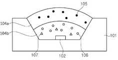
도 1은 본 발명의 일 실시예에 따른 발광 다이오드 패키지를 나타내는 단면도이다. 도 1를 참조하면, 발광 다이오드 패키지는 하우징(101), 발광 다이오드 칩(102), 제1 형광체(105), 제2 형광체(106), 제3 형광체(107) 및 봉지부(104)를 포함한다.1 is a cross-sectional view illustrating a light emitting diode package according to an embodiment of the present invention. Referring to FIG. 1, a light emitting diode package includes a
상기 하우징(101) 상에 발광 다이오드 칩(102), 제1 형광체(105), 제2 형광체(106), 제3 형광체(107) 및 봉지부(104)가 배치될 수 있다. 발광 다이오드 칩(102)은 하우징(101)의 바닥면에 배치될 수 있다, 하우징(101)에는 발광 다이오드 칩(102)에 전력을 입력하기 위한 리드 단자들(미도시)이 설치될 수 있다. 봉지부(104)는 제1, 제2 및 제3 형광체(105, 106, 107)들을 포함하고, 발광 다이오드 칩(102)을 덮을 수 있다.A light emitting
하우징(101)은 일반적인 플라스틱(폴리머) 또는 ABS(acrylonitrile butadiene styrene), LCP(liquid crystalline polymer), PA(polyamide), IPS(polyphenylene sulfide), TPE(thermoplastic elastomer)등으로 형성될 수 있고, 메탈 또는 세라믹으로 형성될 수 있다. 발광 다이오드 칩(102)이 자외선 발광 다이오드 칩인 경우에는, 하우징(101)은 세라믹으로 형성될 수 있다. 하우징(101)이 세라믹인 경우에는, 자외선 발광 다이오드 칩에서 방출된 자외선 광에 의해 세라믹을 포함하는 하우징(101)이 변색되거나 변질될 우려가 없어, 발광 다이오드 패키지의 신뢰성을 유지할 수 있다. 하우징(101)이 메탈인 경우에는, 하우징(101)은 둘 이상의 금속 프레임들을 포함할 수 있고, 금속 프레임들은 서로 절연될 수 있다. 메탈을 포함하는 하우징(101)을 통해, 발광 다이오드 패키지의 방열 능력을 향상시킬 수 있다. 하우징(101)을 형성할 수 있는 물질들을 상기에 언급하였지만, 하우징(101)은 이에 제한되지 않고 다양한 물질들로 형성할 수 있다.The
하우징(101)은 발광 다이오드 칩(102)에서 방출되는 광의 반사를 위하여 경사진 내벽을 포함할 수 있다.The
봉지부(104)는 높은 경도를 가지는 물질로 형성될 수 있다. 구체적으로, 봉지부(104)의 경도는 쇼어 경도(Shore hardness)로 측정했을 시, 측정 수치는 69 내지 71이고, 인덱터(indentor) 유형은 D type일 수 있다. 봉지부(104)는 고경도를 가지기 위하여, 실리콘(silicone), 에폭시(epoxy), PMMA(polymethyl methacrylate), PE(polyethylene) 및 PS(polystyrene) 중 적어도 하나를 포함하는 물질로 형성될 수 있다.The
봉지부(104)는 상술한 물질과 제1, 제2 및 제3 형광체(105, 106, 107)들의 혼합물을 이용한 사출 공정을 통해 형성할 수 있다. 또한 별도의 주형을 이용하여 제작한 다음, 이를 가압 또는 열처리하여 봉지부(104)를 형성할 수 있다. 봉지부(104)는 볼록 렌즈 형태, 평판 형태(미도시) 및 표면에 소정의 요철을 갖는 형태 등 다양한 형상으로 형성할 수 있다. 본 발명에 따른 발광 다이오드 패키지는 볼록 렌즈 형태를 가지는 봉지부(104)를 개시하였지만, 봉지부(104)의 형상은 이에 국한되지 않는다.The
발광 다이오드 칩(102)은 자외선 발광 다이오드 칩 또는 청색 발광 다이오드 칩일 수 있다. 발광 다이오드 칩(102)이 청색 발광 다이오드 칩인 경우에는, 방출하는 광의 피크 파장은 410 내지 490nm 범위 내에 위치할 수 있다. 발광 다이오드 칩(102)이 방출하는 청색광의 피크 파장의 반치폭(full width at half maximum: FWHM)은 40nm 이하 일 수 있다. 본 발명에 따른 발광 다이오드 패키지는 하나의 발광 다이오드 칩(102)이 배치된 형태를 개시하였지만, 배치되는 발광 다이오드 칩(102)의 개수 및 배치 형태는 이에 제한되지 않는다.The light emitting
제1 형광체(105)는 발광 다이오드 칩(102)에 여기되어 녹색광을 방출할 수 있다. 제2 형광체(106) 및 제3 형광체(107)는 발광 다이오드 칩(102)에 여기되어 적색광을 방출할 수 있다.The
제1 형광체(105)가 방출하는 녹색광의 피크 파장은 500 내지 570nm 범위 내에 위치할 수 있다. 제1 형광체(105)는 35nm이하의 반치폭을 가지는 녹색광을 방출할 수 있다. 제1 형광체(105)는 BAM(Ba-Al-Mg) 계열의 형광체, 양자점(quantum dot) 형광체, 실리케이트(Silicate) 계열, 베타-사이알론(beta-SiAlON) 계열, 가넷(Garnet) 계열, LSN 계열 및 불화물 계열 형광체에서 선택된 적어도 하나의 형광체를 포함할 수 있다. 상기 불화물 계열 형광체는 A2MF6:Mn4+의 화학식을 가지는 형광체일 수 있다. 상기 화학식에서 상기 A는 Li, Na, K, Ba, Rb, Cs, Mg, Ca, Ce, Se, NH4 및 Zn 중 하나이고, 상기 M은 Ti, Nd, Ta, Si, Zr, Sn 및 Ge 중 하나일 수 있다. 상기에 제1 형광체(105)의 종류를 서술하였지만, 본 발명에 따른 제1 형광체(105)의 종류는 이로 인해 제한되는 것은 아니다.The peak wavelength of green light emitted by the
녹색광의 반치폭이 좁을수록 높은 색 순도를 가지는 녹색광을 구현할 수 있다. 반치폭이 35㎚ 이상인 경우에는, 발광하는 광의 색 순도가 낮기 때문에 컬러 텔레비전의 방송 방식으로서 채용되고 있는 NTSC(National Television System Committee) 방식의 규격으로 정해져 있는 전체 색 재현 범위의 85% 이상을 재현하기 어렵다. 따라서, 본 발명에 따른 발광 소자가 방출하는 백색광의 85% 이상의 NTSC 색채 포화도를 구현하기 위해, 상기 제1 형광체는 35㎚ 이하의 반치폭을 가지는 녹색광을 방출한다.As the half-width of the green light is narrower, green light having a higher color purity can be realized. When the half width is 35 nm or more, it is difficult to reproduce more than 85% of the total color reproduction range specified by the NTSC (National Television System Committee) standard, which is adopted as a broadcasting method for color television, because the color purity of the emitted light is low. . Accordingly, in order to implement NTSC color saturation of 85% or more of the white light emitted by the light emitting device according to the present invention, the first phosphor emits green light having a half width of 35 nm or less.
제2 형광체(106)는 발광 다이오드 칩(102)에 의해 여기되어 적색광을 방출할 수 있다. 제2 형광체(106)가 방출하는 적색광의 피크 파장은 610 내지 650㎚ 범위 내에서 위치할 수 있다. 제2 형광체(106)는 양자점(quantum dot) 형광체, 황화물계 형광체 및 불화물 계열 형광체에서 선택된 적어도 하나의 형광체를 포함할 수 있다. 불화물 계열 형광체는 A2MF6:Mn4+의 화학식을 가지는 형광체일 수 있다. 상기 화학식에서 상기 A는 Li, Na, K, Ba, Rb, Cs, Mg, Ca, Se 및 Zn 중 하나이고, 상기 M은 Ti, Si, Zr, Sn 및 Ge 중 하나일 수 있다. 제2 형광체(106)는 좁은 반치폭을 가지는 적색광을 방출할 수 있다. 구체적으로, 양자점 형광체의 경우에는 30 내지 40㎚의 반치폭을, 황화물계 형광체인 경우에는 65㎚ 이하의 반치폭을, 불화물 계열 형광체의 경우에는 15㎚ 이하의 반치폭을 가지는 적색광을 방출할 수 있다. 즉, 제2 형광체(106)가 불화물 계열 형광체인 경우에, 가장 좁은 반치폭을 가지는 적색광을 방출할 수 있다.The
제3 형광체(107)는 발광 다이오드 칩(102)에 의해 여기되어 적색광을 방출할 수 있다. 제3 형광체(107)가 방출하는 적색광의 피크 파장은 제2 형광체(106)이 방출하는 적색광의 피크 파장과 다를 수 있다. 구체적으로, 제3 형광체(107)가 방출하는 적색광의 피크 파장은 630 내지 670nm 범위 내에서 위치할 수 있다. 제3 형광체(107)는 질화물계 형광체일 수 있다. 상기 질화물계 형광체는 MSiN2, MSiON2 및 M2Si5N8 화학식으로 표현되는 형광체들 중 적어도 하나를 포함할 수 있으며, 상기 M은 Ca, Sr, Ba, Zn, Mg 및 Eu 중 하나일 수 있다. 또한, 상기 제3 형광체(107)는 양자점(quantum dot) 형광체, 황화물계 형광체 중에서 적어도 하나를 포함할 수 있다.The
본 실시예에 있어서, 제3 형광체(107)는 봉지부(104)에 대하여, 0.1 내지 1wt%의 질량범위를 가질 수 있다. 제3 형광체(107)가 상기 질량범위를 가지므로, 본원 발명에 따른 발광 다이오드 패키지는 85% 이상의 색재현성(NTSC)를 가질 수 있다. 제2 형광체(106)가 불화물 형광체인 경우에, 불화물 형광체는 상대적으로 습기 및 열에 취약하다. 그러나, 제3 형광체(107)이 상술한 형광체들 중 하나인 경우에는 불화물 형광체와 비교하여 상대적으로 습기 및 열에 강하다. 따라서, 제3 형광체(107)가 제2 형광체(106)의 일부를 대신하여 봉지부(104)에 포함되면, 전체적인 형광체들의 내습성 및 내열성을 향상시켜 신뢰성을 향상시킬 수 있다. 그러나, 제3 형광체(107)를 봉지부(104) 내에, 제2 형광체(106)를 대신하여 과도하게 포함시키면, 제3 형광체(107) 및 제2 형광체(106)가 방출하는 적색광의 반치폭이 넓어지므로, 발광 다이오드 패키지의 색재현성이 저하될 수 있다.In this embodiment, the
따라서, 본 발명에 따른 발광 다이오드 패키지는 제3 형광체(107)가 봉지부(104)에 대하여, 0.1 내지 1wt%의 질량범위를 가지고 봉지부(104) 내에 분포되면, 신뢰성을 확보함과 동시에, 85% 이상의 색재현성(NTSC)을 확보할 수 있다. 즉, 제3 형광체(107)가 봉지부(104)에 대하여, 0.1wt% 미만의 질량으로 봉지부(104) 내에 분포되면, 형광체의 신뢰성이 문제될 수 있다. 또한, 제3 형광체(107)가 봉지부(104)에 대하여, 1wt% 초과되는 질량으로 봉지부(104) 내에 분포되면, 형광체가 방출하는 광의 반치폭이 넓어지므로 발광 다이오드 패키지의 색재현성이 문제될 수 있다.Therefore, in the light emitting diode package according to the present invention, when the
상술한 질량 범위 내의 제3 형광체(107)를 포함하는 발광 다이오드 패키지가 방출하는 백색광은 백색광은 CIE 색도도 상의 영역 내에 있는 지점을 형성하는 x 및 y 색좌표를 가지며, 상기 x 색좌표는 0.25 내지 0.32이고, 상기 y 색좌표는 0.22 내지 0.32일 수 있다.The white light emitted by the light emitting diode package including the
도 2는 본 발명의 다른 실시예에 따른 발광 다이오드 패키지를 나타내는 단면도이다. 도 2를 참조하면, 발광 다이오드 패키지는 하우징(101), 발광 다이오드 칩(102), 봉지부(104), 제1 형광체(105), 제2 형광체(106), 제3 형광체(107) 및 버퍼부(109)를 포함한다. 본 실시예에 따른 발광 다이오드 패키지는 버퍼부(109)를 제외하면, 상기 일 실시예에 따른 발광 다이오드 패키지와 대체로 유사하며, 따라서 중복되는 설명은 생략한다.2 is a cross-sectional view illustrating a light emitting diode package according to another exemplary embodiment of the present invention. Referring to FIG. 2, a light emitting diode package includes a
버퍼부(109)는 발광 다이오드 칩(102)과 봉지부(104) 사이에 배치될 수 있다. 버퍼부는 silicone, epoxy, PMMA(polymethyl methacrylate), PE(polyethylene) 및 PS(polystyrene) 중 적어도 하나를 포함하는 물질로 형성될 수 있다. 버퍼부(109)의 경도는 봉지부(104)보다 작을 수 있다. 버퍼부(109)을 이용하여, 발광 다이오드 칩(102)에서 발생하는 열로 인한 봉지부(104)의 열적 스트레스를 방지할 수 있다. 본 실시예에 따른 버퍼부(109)는 발광 다이오드 칩(102) 주변 영역에 배치된 경우를 개시하였지만, 버퍼부(109)는 하우징(101)의 좌측벽과 우측벽 모두와 접하도록 넓은 영역에 배치될 수 도 있다.The
도 3은 본 발명의 또 다른 실시예에 따른 발광 다이오드 패키지를 나타내는 단면도이다. 도 3를 참조하면, 발광 다이오드 패키지는 하우징(101), 발광 다이오드 칩(102), 봉지부(104), 제1 형광체(105), 제2 형광체(106), 제3 형광체(107), 리플렉터(111) 및 베리어 리플렉터(112)를 포함할 수 있다. 본 실시예에 따른 발광 다이오드 패키지는 리플렉터(111) 및 베리어 리플렉터(112)를 제외하면, 상기 일 실시예에 따른 발광 다이오드 패키지와 대체로 유사하며, 따라서 중복되는 설명은 생략한다.3 is a cross-sectional view illustrating a light emitting diode package according to another exemplary embodiment of the present invention. 3, a light emitting diode package includes a
리플렉터(111)는 발광 다이오드 칩(102)과 이격되어 측면에 배치될 수 있다. 리플렉터(111)는 발광 다이오드 칩(102), 제1, 제2 및 제3 형광체(105, 106, 107)에서 방출되는 광의 반사를 극대화하여 발광 효율을 증대시킬 수 있다. 리플렉터(111)는 반사 코팅 필름 및 반사 코팅 물질층 중 어느 하나로 형성될 수 있다. 리플렉터(111)는 내열성 및 내광성이 우수한 무기 재료, 유기 재료, 금속 재료 및 금속 산화물 재료 중에서 적어도 하나로 형성될 수 있다. 일례로, 리플렉터(111)는 알루미늄(Al), 은(Ag), 금(Au), 이산화 티타늄(TiO2) 등과 같이 높은 반사율을 가지는 금속 또는 금속 산화물을 포함하여 구성될 수 있다. 리플렉터(111)는 하우징(101) 상에 금속 또는 금속 산화물을 증착 또는 코팅하여 형성할 수 있으며, 금속 잉크를 인쇄하여 형성할 수도 있다. 또한, 리플렉터(111)는 하우징(101) 상에 반사 필름 또는 반사 시트(sheet)를 접착하여 형성할 수도 있다.The
베리어 리플렉터(112)는 리플렉터(111)를 덮을 수 있다. 베리어 리플렉터(112)는 발광 다이오드 칩(102)에서 방출되는 열로 인한 리플렉터(111)의 열화 등을 방지할 수 있다. 베리어 리플렉터(112)는 내광성 및 반사율이 높은 무기 재료 또는 금속 재료로 형성될 수 있다.The
도 4는 본 발명의 또 다른 실시예에 따른 발광 다이오드 패키지를 나타내는 단면도이다. 도 4를 참조하면, 발광 소자는 하우징(101), 발광 다이오드 칩(102), 봉지부(104), 제1 형광체(105), 제2 형광체(106) 및 제3 형광체(107)를 포함하고, 봉지부(104)는 제1 봉지부(104b) 및 제2 봉지부(104a)를 더 포함할 수 있다. 본 실시예에 따른 발광 다이오드 패키지는 제1 봉지부(104b) 및 제2 봉지부(104a)를 제외하면, 상기 일 실시예에 따른 발광 다이오드 패키지와 대체로 유사하며, 따라서 중복되는 설명은 생략한다.4 is a cross-sectional view illustrating a light emitting diode package according to another exemplary embodiment of the present invention. Referring to FIG. 4, the light emitting device includes a
제1 봉지부(104b)는 발광 다이오드 칩(102)을 덮을 수 있다. 제2 봉지부(104a)는 제1 봉지부(104b)를 덮을 수 있다. 제1 봉지부(104b)는 제2 봉지부(104a)와 동일한 경도를 가지는 물질로 형성되거나, 다른 경도를 가지는 물질로 형성될 수 있다. 제1 봉지부(104b)의 경도는 제2 봉지부(104a)보다 낮을 수 있고, 이 경우, 상술한 실시예의 버퍼부(109)와 동일하게, 발광 다이오드 칩(102)에 인한 열 스트레스를 완화할 수 있다.The
제1 봉지부(104b)는 적색광을 방출하는 제2 형광체(106) 및 제3 형광체(107)를 함유할 수 있다. 제2 봉지부(104a)는 녹색광을 방출하는 제1 형광체(105)를 함유할 수 있다. 장파장을 방출하는 형광체들을 하부에 배치하고, 단파장을 방출하는 형광체들을 상부에 배치하여, 제1 형광체(105)에서 발광된 녹색광이 제2 형광체(106) 및 제3 형광체(107)에 다시 흡수되어 손실되는 것을 방지할 수 있다.The
이상의 설명은 본 발명의 기술 사상을 예시적으로 설명한 것에 불과한 것으로서, 본 발명이 속하는 기술 분야에서 통상의 지식을 가진 자라면 본 발명의 본질적인 특성에서 벗어나지 않는 범위 내에서 다양한 수정, 변경 및 치환이 가능할 것이다. 따라서, 본 발명에 개시된 실시예 및 첨부된 도면들은 본 발명의 기술 사상을 한정하기 위한 것이 아니라 설명하기 위한 것이고, 이러한 실시예 및 첨부된 도면에 의하여 본 발명의 기술 사상의 범위가 한정되는 것은 아니다. 본 발명의 보호 범위는 아래의 청구범위에 의하여 해석되어야 하며, 그와 동등한 범위 내에 있는 모든 기술 사상은 본 발명의 권리범위에 포함되는 것으로 해석되어야 할 것이다.The above description is merely illustrative of the technical idea of the present invention, and those of ordinary skill in the technical field to which the present invention belongs can make various modifications, changes, and substitutions within the scope not departing from the essential characteristics of the present invention. will be. Accordingly, the embodiments disclosed in the present invention and the accompanying drawings are not intended to limit the technical idea of the present invention, but are for illustrative purposes, and the scope of the technical idea of the present invention is not limited by these embodiments and the accompanying drawings. . The scope of protection of the present invention should be construed by the following claims, and all technical ideas within the scope equivalent thereto should be construed as being included in the scope of the present invention.
101: 하우징
102: 발광 다이오드 칩
104: 봉지부
104a: 제1 봉지부
104b: 제2 봉지부
105: 제1 형광체
106: 제2 형광체
107: 제3 형광체
109: 버퍼부
111: 리플렉터
112: 베리어 리플렉터
118: 형광체 플레이트101: housing
102: light emitting diode chip
104: bag
104a: first encapsulation portion
104b: second encapsulation portion
105: first phosphor
106: second phosphor
107: third phosphor
109: buffer unit
111: reflector
112: barrier reflector
118: phosphor plate
Claims (15)
Translated fromKorean상기 하우징에 배치되는 청색 발광 다이오드 칩;
상기 발광 다이오드 칩을 덮는 봉지부;
상기 봉지부 내에 분포되어, 녹색광을 방출하는 제1 형광체;
상기 봉지부 내에 분포되어, 적색광을 방출하는 제2 형광체 및 제3 형광체를 포함하되,
상기 제2 형광체는 A2MF6: Mn4+의 화학식을 가지는 형광체이고, 상기 A는 Li, Na, K, Rb, Ce 및 NH4 중 하나이고, 상기 M은 Si, Ti, Nb 및 Ta 중 하나이며,
상기 제3 형광체는 질화물계 형광체이고, 봉지부에 대하여 0.1 내지 1 wt%의 질량범위를 가지며,
상기 제1 형광체의 녹색광의 피크 파장은 500 내지 570nm 범위 내에 위치하고,
상기 제2 형광체의 적색광의 피크 파장은 610 내지 650nm 범위 내에 위치하며,
상기 제3 형광체의 적색광의 피크 파장은 630 내지 670nm 범위 내에 위치하고,
상기 제2 형광체 및 제3 형광체가 방출하는 적색광은 15nm 이하의 반치폭(FWMH)을 가지는 발광 다이오드 패키지.housing;
A blue light emitting diode chip disposed in the housing;
An encapsulation part covering the light emitting diode chip;
A first phosphor that is distributed in the encapsulation and emits green light;
Including a second phosphor and a third phosphor that are distributed in the encapsulation and emit red light,
The second phosphor is a phosphor havinga formula of A 2 MF6 : Mn4+ , wherein A is one of Li, Na, K, Rb, Ce, and NH4 , and M is one of Si, Ti, Nb and Ta Is one,
The third phosphor is a nitride-based phosphor, and has a mass range of 0.1 to 1 wt% with respect to the encapsulation portion,
The peak wavelength of green light of the first phosphor is located in the range of 500 to 570 nm,
The peak wavelength of the red light of the second phosphor is located in the range of 610 to 650 nm,
The peak wavelength of the red light of the third phosphor is located in the range of 630 to 670 nm,
The red light emitted by the second and third phosphors has a half width (FWMH) of 15 nm or less.
상기 제2 형광체 및 제3 형광체 각각 방출하는 피크 파장은 서로 다른 발광 다이오드 패키지.The method according to claim 1,
A light emitting diode package having different peak wavelengths each of the second and third phosphors.
상기 제1 형광체는 BAM(Ba-Al-Mg) 계열의 형광체, 양자점(quantum dot) 형광체, 실리케이트(Silicate) 계열, 베타-사이알론(beta-SiAlON) 계열, 가넷(Garnet) 계열, LSN 계열 형광체 중 적어도 하나인 발광 다이오드 패키지.The method according to claim 1,
The first phosphor is a BAM (Ba-Al-Mg)-based phosphor, a quantum dot phosphor, a silicate-based, beta-SiAlON-based, Garnet-based, LSN-based phosphor. A light emitting diode package that is at least one of.
상기 질화물계 형광체는 MSiN2, MSiON2 및 M2Si5N8 화학식으로 표현되는 형광체들 중 적어도 하나를 포함하고, 상기 M은 Ca, Sr, Ba, Zn, Mg 및 Eu 중 하나인 발광 다이오드 패키지.The method according to claim 1,
The nitride-based phosphor includesat least one of phosphors represented by the formula MSiN 2 , MSiON2 and M2 Si5 N8 , wherein M is one of Ca, Sr, Ba, Zn, Mg, and Eu. .
상기 봉지부는 실리콘, 에폭시, PMMA, PE 및 PS 중 적어도 하나를 포함하는 발광 다이오드 패키지.The method according to claim 1,
The encapsulation part includes at least one of silicon, epoxy, PMMA, PE, and PS.
상기 발광 다이오드 칩, 상기 제1 형광체, 상기 제2 형광체 및 상기 제3 형광체에서 방출되는 광의 합성에 의해 백색광이 형성되고,
상기 백색광은 85% 이상의 NTSC(national television system committee) 색채 포화도를 가지는 발광 다이오드 패키지.The method according to claim 1,
White light is formed by synthesis of light emitted from the light emitting diode chip, the first phosphor, the second phosphor, and the third phosphor,
The white light is a light emitting diode package having an NTSC (national television system committee) color saturation of 85% or more.
상기 백색광은 백색광은 CIE 색도도 상의 영역 내에 있는 지점을 형성하는 x 및 y 색좌표를 가지며,
상기 x 색좌표는 0.25 내지 0.32이고, 상기 y 색좌표는 0.22 내지 0.32인 발광 다이오드 패키지.The method of claim 9,
The white light has x and y color coordinates forming a point within the region on the CIE chromaticity diagram,
The x color coordinate is 0.25 to 0.32, and the y color coordinate is 0.22 to 0.32.
상기 봉지부와 상기 발광 다이오드 칩 사이에 배치되는 버퍼부를 더 포함하되,
상기 버퍼부는 상기 봉지부보다 낮은 경도를 가지는 발광 다이오드 패키지.The method according to claim 1,
Further comprising a buffer portion disposed between the encapsulation portion and the light emitting diode chip,
The light emitting diode package of the buffer part has a lower hardness than the encapsulation part.
상기 봉지부는 상기 발광 다이오드 칩을 덮는 제1 봉지부; 및
상기 제1 봉지부를 덮는 제2 봉지부를 포함하되,
상기 제1 봉지부는 상기 제2 형광체 및 제3 형광체를 함유하고,
상기 제2 봉지부는 상기 제1 형광체를 함유하는 발광 다이오드 패키지.The method according to claim 1,
The encapsulation part comprises: a first encapsulation part covering the light emitting diode chip; And
Including a second sealing portion covering the first sealing portion,
The first encapsulation portion contains the second phosphor and the third phosphor,
The light emitting diode package containing the first phosphor in the second encapsulation part.
상기 하우징은 상기 발광 다이오드 칩에서 방출된 광을 반사하는 리플렉터를 포함하는 발광 다이오드 패키지.The method according to claim 1,
The housing is a light emitting diode package including a reflector reflecting light emitted from the light emitting diode chip.
상기 하우징은 상기 리플렉터를 덮는 베리어 리플렉터를 더 포함하는 발광 다이오드 패키지.The method of claim 14,
The housing further includes a barrier reflector covering the reflector.
Priority Applications (2)
| Application Number | Priority Date | Filing Date | Title |
|---|---|---|---|
| KR1020140135337AKR102256594B1 (en) | 2014-10-07 | 2014-10-07 | Light emitting diode package |
| PCT/KR2015/010589WO2016056836A1 (en) | 2014-10-07 | 2015-10-07 | Light emitting device |
Applications Claiming Priority (1)
| Application Number | Priority Date | Filing Date | Title |
|---|---|---|---|
| KR1020140135337AKR102256594B1 (en) | 2014-10-07 | 2014-10-07 | Light emitting diode package |
Publications (2)
| Publication Number | Publication Date |
|---|---|
| KR20160041469A KR20160041469A (en) | 2016-04-18 |
| KR102256594B1true KR102256594B1 (en) | 2021-05-26 |
Family
ID=55916579
Family Applications (1)
| Application Number | Title | Priority Date | Filing Date |
|---|---|---|---|
| KR1020140135337AActiveKR102256594B1 (en) | 2014-10-07 | 2014-10-07 | Light emitting diode package |
Country Status (1)
| Country | Link |
|---|---|
| KR (1) | KR102256594B1 (en) |
Families Citing this family (2)
| Publication number | Priority date | Publication date | Assignee | Title |
|---|---|---|---|---|
| KR102578085B1 (en)* | 2016-04-29 | 2023-09-14 | 쑤저우 레킨 세미컨덕터 컴퍼니 리미티드 | Phosphor composition, light emitting device package and lighting apparatus including the same |
| CN111986565A (en)* | 2019-05-21 | 2020-11-24 | 展晶科技(深圳)有限公司 | Light source device and display |
Citations (3)
| Publication number | Priority date | Publication date | Assignee | Title |
|---|---|---|---|---|
| KR100529591B1 (en) | 2003-02-05 | 2005-11-17 | 서울반도체 주식회사 | White Light Emitting Device having high brightness |
| JP2010209311A (en)* | 2008-09-05 | 2010-09-24 | Mitsubishi Chemicals Corp | Phosphor and process for producing the same, phosphor-containing composition and light-emitting device using the same, and image display and lighting apparatus using light-emitting device |
| JP2012104814A (en)* | 2010-10-15 | 2012-05-31 | Mitsubishi Chemicals Corp | White light-emitting device and lighting fixture |
Family Cites Families (3)
| Publication number | Priority date | Publication date | Assignee | Title |
|---|---|---|---|---|
| JP2002314143A (en)* | 2001-04-09 | 2002-10-25 | Toshiba Corp | Light emitting device |
| US7258816B2 (en) | 2002-03-22 | 2007-08-21 | Nichia Corporation | Nitride phosphor and method for preparation thereof, and light emitting device |
| KR100558080B1 (en) | 2002-10-09 | 2006-03-07 | 서울반도체 주식회사 | Phosphor, Light Emitting Diode Using the Same, and Manufacturing Method Thereof |
- 2014
- 2014-10-07KRKR1020140135337Apatent/KR102256594B1/enactiveActive
Patent Citations (3)
| Publication number | Priority date | Publication date | Assignee | Title |
|---|---|---|---|---|
| KR100529591B1 (en) | 2003-02-05 | 2005-11-17 | 서울반도체 주식회사 | White Light Emitting Device having high brightness |
| JP2010209311A (en)* | 2008-09-05 | 2010-09-24 | Mitsubishi Chemicals Corp | Phosphor and process for producing the same, phosphor-containing composition and light-emitting device using the same, and image display and lighting apparatus using light-emitting device |
| JP2012104814A (en)* | 2010-10-15 | 2012-05-31 | Mitsubishi Chemicals Corp | White light-emitting device and lighting fixture |
Also Published As
| Publication number | Publication date |
|---|---|
| KR20160041469A (en) | 2016-04-18 |
Similar Documents
| Publication | Publication Date | Title |
|---|---|---|
| US12349519B2 (en) | Light emitting device | |
| KR102184381B1 (en) | Light emitting device having uv light diode and lighting apparatus including the same | |
| KR102596919B1 (en) | Light emitting diode package | |
| CN105374922B (en) | Light emitting diode package and manufacturing method thereof | |
| US9590149B2 (en) | Lighting emitting device | |
| KR102273653B1 (en) | Light emitting diode package | |
| KR102191211B1 (en) | Light emitting diode package | |
| KR102648863B1 (en) | Light emitting diode package | |
| JP2016042579A (en) | Light emitting diode package and manufacturing method thereof | |
| KR102256594B1 (en) | Light emitting diode package | |
| KR20210100057A (en) | Light emitting device | |
| KR20210031874A (en) | Light emitting diode package | |
| KR102135626B1 (en) | Light emitting device having uv light diode | |
| KR20160021491A (en) | Light emitting diode package | |
| KR102310038B1 (en) | White light emitting device | |
| KR102288377B1 (en) | Light emitting device |
Legal Events
| Date | Code | Title | Description |
|---|---|---|---|
| PA0109 | Patent application | Patent event code:PA01091R01D Comment text:Patent Application Patent event date:20141007 | |
| PG1501 | Laying open of application | ||
| A201 | Request for examination | ||
| PA0201 | Request for examination | Patent event code:PA02012R01D Patent event date:20191007 Comment text:Request for Examination of Application Patent event code:PA02011R01I Patent event date:20141007 Comment text:Patent Application | |
| E902 | Notification of reason for refusal | ||
| PE0902 | Notice of grounds for rejection | Comment text:Notification of reason for refusal Patent event date:20200904 Patent event code:PE09021S01D | |
| E701 | Decision to grant or registration of patent right | ||
| PE0701 | Decision of registration | Patent event code:PE07011S01D Comment text:Decision to Grant Registration Patent event date:20210219 | |
| GRNT | Written decision to grant | ||
| PR0701 | Registration of establishment | Comment text:Registration of Establishment Patent event date:20210520 Patent event code:PR07011E01D | |
| PR1002 | Payment of registration fee | Payment date:20210521 End annual number:3 Start annual number:1 | |
| PG1601 | Publication of registration | ||
| PR1001 | Payment of annual fee | Payment date:20240326 Start annual number:4 End annual number:4 |