KR102252563B1 - Semiconductor device - Google Patents
Semiconductor deviceDownload PDFInfo
- Publication number
- KR102252563B1 KR102252563B1KR1020200154707AKR20200154707AKR102252563B1KR 102252563 B1KR102252563 B1KR 102252563B1KR 1020200154707 AKR1020200154707 AKR 1020200154707AKR 20200154707 AKR20200154707 AKR 20200154707AKR 102252563 B1KR102252563 B1KR 102252563B1
- Authority
- KR
- South Korea
- Prior art keywords
- terminal
- transistor
- potential
- electrically connected
- node
- Prior art date
- Legal status (The legal status is an assumption and is not a legal conclusion. Google has not performed a legal analysis and makes no representation as to the accuracy of the status listed.)
- Active
Links
- 239000004065semiconductorSubstances0.000titleclaimsdescription191
- 238000007667floatingMethods0.000abstractdescription25
- 239000010408filmSubstances0.000description165
- 239000010410layerSubstances0.000description122
- 239000003990capacitorSubstances0.000description66
- 230000006870functionEffects0.000description65
- 239000004973liquid crystal related substanceSubstances0.000description45
- 239000000758substrateSubstances0.000description44
- 238000000034methodMethods0.000description35
- 238000010586diagramMethods0.000description32
- IJGRMHOSHXDMSA-UHFFFAOYSA-NAtomic nitrogenChemical compoundN#NIJGRMHOSHXDMSA-UHFFFAOYSA-N0.000description26
- 230000008878couplingEffects0.000description21
- 238000010168coupling processMethods0.000description21
- 238000005859coupling reactionMethods0.000description21
- 239000012535impuritySubstances0.000description21
- 238000004519manufacturing processMethods0.000description20
- 239000013078crystalSubstances0.000description17
- 229910045601alloyInorganic materials0.000description16
- 239000000956alloySubstances0.000description16
- 229910052782aluminiumInorganic materials0.000description15
- XAGFODPZIPBFFR-UHFFFAOYSA-NaluminiumChemical compound[Al]XAGFODPZIPBFFR-UHFFFAOYSA-N0.000description15
- 230000007274generation of a signal involved in cell-cell signalingEffects0.000description14
- BLRPTPMANUNPDV-UHFFFAOYSA-NSilaneChemical compound[SiH4]BLRPTPMANUNPDV-UHFFFAOYSA-N0.000description13
- 238000005530etchingMethods0.000description13
- 229910052757nitrogenInorganic materials0.000description13
- 229910052990silicon hydrideInorganic materials0.000description13
- PXHVJJICTQNCMI-UHFFFAOYSA-NNickelChemical compound[Ni]PXHVJJICTQNCMI-UHFFFAOYSA-N0.000description12
- ZOXJGFHDIHLPTG-UHFFFAOYSA-NBoronChemical compound[B]ZOXJGFHDIHLPTG-UHFFFAOYSA-N0.000description11
- UFHFLCQGNIYNRP-UHFFFAOYSA-NHydrogenChemical compound[H][H]UFHFLCQGNIYNRP-UHFFFAOYSA-N0.000description11
- 229910052796boronInorganic materials0.000description11
- 239000001257hydrogenSubstances0.000description11
- 229910052739hydrogenInorganic materials0.000description11
- OKTJSMMVPCPJKN-UHFFFAOYSA-NCarbonChemical compound[C]OKTJSMMVPCPJKN-UHFFFAOYSA-N0.000description10
- OAICVXFJPJFONN-UHFFFAOYSA-NPhosphorusChemical compound[P]OAICVXFJPJFONN-UHFFFAOYSA-N0.000description10
- 230000015572biosynthetic processEffects0.000description10
- 229910052799carbonInorganic materials0.000description10
- 239000000463materialSubstances0.000description10
- 229910052698phosphorusInorganic materials0.000description10
- 239000011574phosphorusSubstances0.000description10
- 239000007789gasSubstances0.000description9
- 239000010409thin filmSubstances0.000description9
- 239000000460chlorineSubstances0.000description8
- 230000003071parasitic effectEffects0.000description8
- 238000005268plasma chemical vapour depositionMethods0.000description8
- XUIMIQQOPSSXEZ-UHFFFAOYSA-NSiliconChemical compound[Si]XUIMIQQOPSSXEZ-UHFFFAOYSA-N0.000description7
- 230000006866deteriorationEffects0.000description7
- 230000000694effectsEffects0.000description7
- 229910052710siliconInorganic materials0.000description7
- 239000010703siliconSubstances0.000description7
- 238000004544sputter depositionMethods0.000description7
- XKRFYHLGVUSROY-UHFFFAOYSA-NArgonChemical compound[Ar]XKRFYHLGVUSROY-UHFFFAOYSA-N0.000description6
- RTAQQCXQSZGOHL-UHFFFAOYSA-NTitaniumChemical compound[Ti]RTAQQCXQSZGOHL-UHFFFAOYSA-N0.000description6
- QVGXLLKOCUKJST-UHFFFAOYSA-Natomic oxygenChemical compound[O]QVGXLLKOCUKJST-UHFFFAOYSA-N0.000description6
- 229910052759nickelInorganic materials0.000description6
- 239000001301oxygenSubstances0.000description6
- 229910052760oxygenInorganic materials0.000description6
- 239000010936titaniumSubstances0.000description6
- 229910052719titaniumInorganic materials0.000description6
- ZOKXTWBITQBERF-UHFFFAOYSA-NMolybdenumChemical compound[Mo]ZOKXTWBITQBERF-UHFFFAOYSA-N0.000description5
- 229910052750molybdenumInorganic materials0.000description5
- 239000011733molybdenumSubstances0.000description5
- 239000012071phaseSubstances0.000description5
- QGZKDVFQNNGYKY-UHFFFAOYSA-NAmmoniaChemical compoundNQGZKDVFQNNGYKY-UHFFFAOYSA-N0.000description4
- WKBOTKDWSSQWDR-UHFFFAOYSA-NBromine atomChemical compound[Br]WKBOTKDWSSQWDR-UHFFFAOYSA-N0.000description4
- ZAMOUSCENKQFHK-UHFFFAOYSA-NChlorine atomChemical compound[Cl]ZAMOUSCENKQFHK-UHFFFAOYSA-N0.000description4
- PXGOKWXKJXAPGV-UHFFFAOYSA-NFluorineChemical compoundFFPXGOKWXKJXAPGV-UHFFFAOYSA-N0.000description4
- XEEYBQQBJWHFJM-UHFFFAOYSA-NIronChemical compound[Fe]XEEYBQQBJWHFJM-UHFFFAOYSA-N0.000description4
- KDLHZDBZIXYQEI-UHFFFAOYSA-NPalladiumChemical compound[Pd]KDLHZDBZIXYQEI-UHFFFAOYSA-N0.000description4
- GDTBXPJZTBHREO-UHFFFAOYSA-NbromineSubstancesBrBrGDTBXPJZTBHREO-UHFFFAOYSA-N0.000description4
- 229910052794bromiumInorganic materials0.000description4
- 229910052801chlorineInorganic materials0.000description4
- 229910052731fluorineInorganic materials0.000description4
- 239000011737fluorineSubstances0.000description4
- AMGQUBHHOARCQH-UHFFFAOYSA-Nindium;oxotinChemical compound[In].[Sn]=OAMGQUBHHOARCQH-UHFFFAOYSA-N0.000description4
- 150000004767nitridesChemical class0.000description4
- BASFCYQUMIYNBI-UHFFFAOYSA-NplatinumChemical compound[Pt]BASFCYQUMIYNBI-UHFFFAOYSA-N0.000description4
- 239000002356single layerSubstances0.000description4
- ZCYVEMRRCGMTRW-UHFFFAOYSA-N7553-56-2Chemical compound[I]ZCYVEMRRCGMTRW-UHFFFAOYSA-N0.000description3
- RYGMFSIKBFXOCR-UHFFFAOYSA-NCopperChemical compound[Cu]RYGMFSIKBFXOCR-UHFFFAOYSA-N0.000description3
- BQCADISMDOOEFD-UHFFFAOYSA-NSilverChemical compound[Ag]BQCADISMDOOEFD-UHFFFAOYSA-N0.000description3
- 229910052786argonInorganic materials0.000description3
- 239000012298atmosphereSubstances0.000description3
- 238000004364calculation methodMethods0.000description3
- 230000008859changeEffects0.000description3
- 238000005229chemical vapour depositionMethods0.000description3
- 229910052802copperInorganic materials0.000description3
- 239000010949copperSubstances0.000description3
- 230000003111delayed effectEffects0.000description3
- 238000007865dilutingMethods0.000description3
- 230000005684electric fieldEffects0.000description3
- 239000011521glassSubstances0.000description3
- PCHJSUWPFVWCPO-UHFFFAOYSA-NgoldChemical compound[Au]PCHJSUWPFVWCPO-UHFFFAOYSA-N0.000description3
- 229910052737goldInorganic materials0.000description3
- 239000010931goldSubstances0.000description3
- 239000001307heliumSubstances0.000description3
- 229910052734heliumInorganic materials0.000description3
- SWQJXJOGLNCZEY-UHFFFAOYSA-Nhelium atomChemical compound[He]SWQJXJOGLNCZEY-UHFFFAOYSA-N0.000description3
- 239000011229interlayerSubstances0.000description3
- 239000011630iodineSubstances0.000description3
- 229910052740iodineInorganic materials0.000description3
- 229910052743kryptonInorganic materials0.000description3
- DNNSSWSSYDEUBZ-UHFFFAOYSA-Nkrypton atomChemical compound[Kr]DNNSSWSSYDEUBZ-UHFFFAOYSA-N0.000description3
- 230000007257malfunctionEffects0.000description3
- 239000011159matrix materialSubstances0.000description3
- 239000000203mixtureSubstances0.000description3
- 229910052754neonInorganic materials0.000description3
- GKAOGPIIYCISHV-UHFFFAOYSA-Nneon atomChemical compound[Ne]GKAOGPIIYCISHV-UHFFFAOYSA-N0.000description3
- 230000008569processEffects0.000description3
- VYPSYNLAJGMNEJ-UHFFFAOYSA-Nsilicon dioxideInorganic materialsO=[Si]=OVYPSYNLAJGMNEJ-UHFFFAOYSA-N0.000description3
- 229910052709silverInorganic materials0.000description3
- 239000004332silverSubstances0.000description3
- VYZAMTAEIAYCRO-UHFFFAOYSA-NChromiumChemical compound[Cr]VYZAMTAEIAYCRO-UHFFFAOYSA-N0.000description2
- VEXZGXHMUGYJMC-UHFFFAOYSA-NHydrochloric acidChemical compoundClVEXZGXHMUGYJMC-UHFFFAOYSA-N0.000description2
- 229910052581Si3N4Inorganic materials0.000description2
- 229910021529ammoniaInorganic materials0.000description2
- 229910021417amorphous siliconInorganic materials0.000description2
- SLLGVCUQYRMELA-UHFFFAOYSA-NchlorosiliconChemical compoundCl[Si]SLLGVCUQYRMELA-UHFFFAOYSA-N0.000description2
- 229910052804chromiumInorganic materials0.000description2
- 239000011651chromiumSubstances0.000description2
- 229910017052cobaltInorganic materials0.000description2
- 239000010941cobaltSubstances0.000description2
- GUTLYIVDDKVIGB-UHFFFAOYSA-Ncobalt atomChemical compound[Co]GUTLYIVDDKVIGB-UHFFFAOYSA-N0.000description2
- 238000000151depositionMethods0.000description2
- 239000005262ferroelectric liquid crystals (FLCs)Substances0.000description2
- 238000010438heat treatmentMethods0.000description2
- 229910052742ironInorganic materials0.000description2
- 238000003475laminationMethods0.000description2
- WPBNNNQJVZRUHP-UHFFFAOYSA-Lmanganese(2+);methyl n-[[2-(methoxycarbonylcarbamothioylamino)phenyl]carbamothioyl]carbamate;n-[2-(sulfidocarbothioylamino)ethyl]carbamodithioateChemical compound[Mn+2].[S-]C(=S)NCCNC([S-])=S.COC(=O)NC(=S)NC1=CC=CC=C1NC(=S)NC(=O)OCWPBNNNQJVZRUHP-UHFFFAOYSA-L0.000description2
- 229910052751metalInorganic materials0.000description2
- 239000002184metalSubstances0.000description2
- 229910021424microcrystalline siliconInorganic materials0.000description2
- 229910052763palladiumInorganic materials0.000description2
- 238000000206photolithographyMethods0.000description2
- 229910052697platinumInorganic materials0.000description2
- 229910021420polycrystalline siliconInorganic materials0.000description2
- 229920000728polyesterPolymers0.000description2
- -1polypropylenePolymers0.000description2
- 238000007639printingMethods0.000description2
- HQVNEWCFYHHQES-UHFFFAOYSA-Nsilicon nitrideChemical compoundN12[Si]34N5[Si]62N3[Si]51N64HQVNEWCFYHHQES-UHFFFAOYSA-N0.000description2
- 229910052814silicon oxideInorganic materials0.000description2
- 239000007790solid phaseSubstances0.000description2
- 230000001360synchronised effectEffects0.000description2
- WFKWXMTUELFFGS-UHFFFAOYSA-NtungstenChemical compound[W]WFKWXMTUELFFGS-UHFFFAOYSA-N0.000description2
- 229910052721tungstenInorganic materials0.000description2
- 239000010937tungstenSubstances0.000description2
- 238000001771vacuum depositionMethods0.000description2
- 238000007740vapor depositionMethods0.000description2
- YVTHLONGBIQYBO-UHFFFAOYSA-Nzinc indium(3+) oxygen(2-)Chemical compound[O--].[Zn++].[In+3]YVTHLONGBIQYBO-UHFFFAOYSA-N0.000description2
- 239000004695Polyether sulfoneSubstances0.000description1
- 239000004743PolypropyleneSubstances0.000description1
- 229910003902SiCl 4Inorganic materials0.000description1
- BZHJMEDXRYGGRV-UHFFFAOYSA-NVinyl chlorideChemical compoundClC=CBZHJMEDXRYGGRV-UHFFFAOYSA-N0.000description1
- 239000002313adhesive filmSubstances0.000description1
- 150000001408amidesChemical class0.000description1
- 230000015556catabolic processEffects0.000description1
- 239000003054catalystSubstances0.000description1
- 238000004891communicationMethods0.000description1
- 239000002178crystalline materialSubstances0.000description1
- 238000002425crystallisationMethods0.000description1
- 230000007423decreaseEffects0.000description1
- 230000008021depositionEffects0.000description1
- BUMGIEFFCMBQDG-UHFFFAOYSA-NdichlorosiliconChemical compoundCl[Si]ClBUMGIEFFCMBQDG-UHFFFAOYSA-N0.000description1
- 238000009792diffusion processMethods0.000description1
- 238000010790dilutionMethods0.000description1
- 239000012895dilutionSubstances0.000description1
- 238000007599dischargingMethods0.000description1
- 238000005516engineering processMethods0.000description1
- 239000002657fibrous materialSubstances0.000description1
- 238000010304firingMethods0.000description1
- 229910052736halogenInorganic materials0.000description1
- 150000002367halogensChemical class0.000description1
- 230000006872improvementEffects0.000description1
- PNDPGZBMCMUPRI-UHFFFAOYSA-NiodineChemical compoundIIPNDPGZBMCMUPRI-UHFFFAOYSA-N0.000description1
- 230000001678irradiating effectEffects0.000description1
- 238000010030laminatingMethods0.000description1
- 238000005499laser crystallizationMethods0.000description1
- 239000007791liquid phaseSubstances0.000description1
- 238000004518low pressure chemical vapour depositionMethods0.000description1
- 230000007246mechanismEffects0.000description1
- 238000002844meltingMethods0.000description1
- 230000008018meltingEffects0.000description1
- 239000013081microcrystalSubstances0.000description1
- 238000002156mixingMethods0.000description1
- 230000003287optical effectEffects0.000description1
- 239000002245particleSubstances0.000description1
- 229920003023plasticPolymers0.000description1
- 239000004033plasticSubstances0.000description1
- 229920001230polyarylatePolymers0.000description1
- 239000004417polycarbonateSubstances0.000description1
- 229920000515polycarbonatePolymers0.000description1
- 229920006393polyether sulfonePolymers0.000description1
- 229920001155polypropylenePolymers0.000description1
- 229920005591polysiliconPolymers0.000description1
- 239000004800polyvinyl chlorideSubstances0.000description1
- 229920000915polyvinyl chloridePolymers0.000description1
- 229920002620polyvinyl fluoridePolymers0.000description1
- 230000002250progressing effectEffects0.000description1
- 239000010453quartzSubstances0.000description1
- 230000005855radiationEffects0.000description1
- 238000007348radical reactionMethods0.000description1
- 239000002994raw materialSubstances0.000description1
- 230000006798recombinationEffects0.000description1
- 230000009467reductionEffects0.000description1
- 238000007650screen-printingMethods0.000description1
- 235000013599spicesNutrition0.000description1
- 238000003860storageMethods0.000description1
- 125000000391vinyl groupChemical group[H]C([*])=C([H])[H]0.000description1
- 229920002554vinyl polymerPolymers0.000description1
- XLYOFNOQVPJJNP-UHFFFAOYSA-NwaterSubstancesOXLYOFNOQVPJJNP-UHFFFAOYSA-N0.000description1
Images


Classifications
- G—PHYSICS
- G09—EDUCATION; CRYPTOGRAPHY; DISPLAY; ADVERTISING; SEALS
- G09G—ARRANGEMENTS OR CIRCUITS FOR CONTROL OF INDICATING DEVICES USING STATIC MEANS TO PRESENT VARIABLE INFORMATION
- G09G3/00—Control arrangements or circuits, of interest only in connection with visual indicators other than cathode-ray tubes
- G09G3/20—Control arrangements or circuits, of interest only in connection with visual indicators other than cathode-ray tubes for presentation of an assembly of a number of characters, e.g. a page, by composing the assembly by combination of individual elements arranged in a matrix no fixed position being assigned to or needed to be assigned to the individual characters or partial characters
- G09G3/34—Control arrangements or circuits, of interest only in connection with visual indicators other than cathode-ray tubes for presentation of an assembly of a number of characters, e.g. a page, by composing the assembly by combination of individual elements arranged in a matrix no fixed position being assigned to or needed to be assigned to the individual characters or partial characters by control of light from an independent source
- G09G3/36—Control arrangements or circuits, of interest only in connection with visual indicators other than cathode-ray tubes for presentation of an assembly of a number of characters, e.g. a page, by composing the assembly by combination of individual elements arranged in a matrix no fixed position being assigned to or needed to be assigned to the individual characters or partial characters by control of light from an independent source using liquid crystals
- G09G3/3611—Control of matrices with row and column drivers
- G09G3/3674—Details of drivers for scan electrodes
- G09G3/3677—Details of drivers for scan electrodes suitable for active matrices only
- G—PHYSICS
- G11—INFORMATION STORAGE
- G11C—STATIC STORES
- G11C19/00—Digital stores in which the information is moved stepwise, e.g. shift registers
- G11C19/18—Digital stores in which the information is moved stepwise, e.g. shift registers using capacitors as main elements of the stages
- G11C19/182—Digital stores in which the information is moved stepwise, e.g. shift registers using capacitors as main elements of the stages in combination with semiconductor elements, e.g. bipolar transistors, diodes
- G11C19/184—Digital stores in which the information is moved stepwise, e.g. shift registers using capacitors as main elements of the stages in combination with semiconductor elements, e.g. bipolar transistors, diodes with field-effect transistors, e.g. MOS-FET
- G—PHYSICS
- G02—OPTICS
- G02F—OPTICAL DEVICES OR ARRANGEMENTS FOR THE CONTROL OF LIGHT BY MODIFICATION OF THE OPTICAL PROPERTIES OF THE MEDIA OF THE ELEMENTS INVOLVED THEREIN; NON-LINEAR OPTICS; FREQUENCY-CHANGING OF LIGHT; OPTICAL LOGIC ELEMENTS; OPTICAL ANALOGUE/DIGITAL CONVERTERS
- G02F1/00—Devices or arrangements for the control of the intensity, colour, phase, polarisation or direction of light arriving from an independent light source, e.g. switching, gating or modulating; Non-linear optics
- G02F1/01—Devices or arrangements for the control of the intensity, colour, phase, polarisation or direction of light arriving from an independent light source, e.g. switching, gating or modulating; Non-linear optics for the control of the intensity, phase, polarisation or colour
- G02F1/13—Devices or arrangements for the control of the intensity, colour, phase, polarisation or direction of light arriving from an independent light source, e.g. switching, gating or modulating; Non-linear optics for the control of the intensity, phase, polarisation or colour based on liquid crystals, e.g. single liquid crystal display cells
- G02F1/133—Constructional arrangements; Operation of liquid crystal cells; Circuit arrangements
- G02F1/136—Liquid crystal cells structurally associated with a semi-conducting layer or substrate, e.g. cells forming part of an integrated circuit
- G—PHYSICS
- G09—EDUCATION; CRYPTOGRAPHY; DISPLAY; ADVERTISING; SEALS
- G09G—ARRANGEMENTS OR CIRCUITS FOR CONTROL OF INDICATING DEVICES USING STATIC MEANS TO PRESENT VARIABLE INFORMATION
- G09G3/00—Control arrangements or circuits, of interest only in connection with visual indicators other than cathode-ray tubes
- G09G3/20—Control arrangements or circuits, of interest only in connection with visual indicators other than cathode-ray tubes for presentation of an assembly of a number of characters, e.g. a page, by composing the assembly by combination of individual elements arranged in a matrix no fixed position being assigned to or needed to be assigned to the individual characters or partial characters
- G09G3/34—Control arrangements or circuits, of interest only in connection with visual indicators other than cathode-ray tubes for presentation of an assembly of a number of characters, e.g. a page, by composing the assembly by combination of individual elements arranged in a matrix no fixed position being assigned to or needed to be assigned to the individual characters or partial characters by control of light from an independent source
- G09G3/36—Control arrangements or circuits, of interest only in connection with visual indicators other than cathode-ray tubes for presentation of an assembly of a number of characters, e.g. a page, by composing the assembly by combination of individual elements arranged in a matrix no fixed position being assigned to or needed to be assigned to the individual characters or partial characters by control of light from an independent source using liquid crystals
- G09G3/3611—Control of matrices with row and column drivers
- G09G3/3648—Control of matrices with row and column drivers using an active matrix
- G—PHYSICS
- G11—INFORMATION STORAGE
- G11C—STATIC STORES
- G11C19/00—Digital stores in which the information is moved stepwise, e.g. shift registers
- G11C19/28—Digital stores in which the information is moved stepwise, e.g. shift registers using semiconductor elements
- H—ELECTRICITY
- H10—SEMICONDUCTOR DEVICES; ELECTRIC SOLID-STATE DEVICES NOT OTHERWISE PROVIDED FOR
- H10D—INORGANIC ELECTRIC SEMICONDUCTOR DEVICES
- H10D86/00—Integrated devices formed in or on insulating or conducting substrates, e.g. formed in silicon-on-insulator [SOI] substrates or on stainless steel or glass substrates
- H10D86/40—Integrated devices formed in or on insulating or conducting substrates, e.g. formed in silicon-on-insulator [SOI] substrates or on stainless steel or glass substrates characterised by multiple TFTs
- H10D86/421—Integrated devices formed in or on insulating or conducting substrates, e.g. formed in silicon-on-insulator [SOI] substrates or on stainless steel or glass substrates characterised by multiple TFTs having a particular composition, shape or crystalline structure of the active layer
- H10D86/423—Integrated devices formed in or on insulating or conducting substrates, e.g. formed in silicon-on-insulator [SOI] substrates or on stainless steel or glass substrates characterised by multiple TFTs having a particular composition, shape or crystalline structure of the active layer comprising semiconductor materials not belonging to the Group IV, e.g. InGaZnO
- H—ELECTRICITY
- H10—SEMICONDUCTOR DEVICES; ELECTRIC SOLID-STATE DEVICES NOT OTHERWISE PROVIDED FOR
- H10D—INORGANIC ELECTRIC SEMICONDUCTOR DEVICES
- H10D86/00—Integrated devices formed in or on insulating or conducting substrates, e.g. formed in silicon-on-insulator [SOI] substrates or on stainless steel or glass substrates
- H10D86/40—Integrated devices formed in or on insulating or conducting substrates, e.g. formed in silicon-on-insulator [SOI] substrates or on stainless steel or glass substrates characterised by multiple TFTs
- H10D86/481—Integrated devices formed in or on insulating or conducting substrates, e.g. formed in silicon-on-insulator [SOI] substrates or on stainless steel or glass substrates characterised by multiple TFTs integrated with passive devices, e.g. auxiliary capacitors
- H—ELECTRICITY
- H10—SEMICONDUCTOR DEVICES; ELECTRIC SOLID-STATE DEVICES NOT OTHERWISE PROVIDED FOR
- H10D—INORGANIC ELECTRIC SEMICONDUCTOR DEVICES
- H10D86/00—Integrated devices formed in or on insulating or conducting substrates, e.g. formed in silicon-on-insulator [SOI] substrates or on stainless steel or glass substrates
- H10D86/40—Integrated devices formed in or on insulating or conducting substrates, e.g. formed in silicon-on-insulator [SOI] substrates or on stainless steel or glass substrates characterised by multiple TFTs
- H10D86/60—Integrated devices formed in or on insulating or conducting substrates, e.g. formed in silicon-on-insulator [SOI] substrates or on stainless steel or glass substrates characterised by multiple TFTs wherein the TFTs are in active matrices
- G—PHYSICS
- G09—EDUCATION; CRYPTOGRAPHY; DISPLAY; ADVERTISING; SEALS
- G09G—ARRANGEMENTS OR CIRCUITS FOR CONTROL OF INDICATING DEVICES USING STATIC MEANS TO PRESENT VARIABLE INFORMATION
- G09G2230/00—Details of flat display driving waveforms
- G—PHYSICS
- G09—EDUCATION; CRYPTOGRAPHY; DISPLAY; ADVERTISING; SEALS
- G09G—ARRANGEMENTS OR CIRCUITS FOR CONTROL OF INDICATING DEVICES USING STATIC MEANS TO PRESENT VARIABLE INFORMATION
- G09G2300/00—Aspects of the constitution of display devices
- G09G2300/08—Active matrix structure, i.e. with use of active elements, inclusive of non-linear two terminal elements, in the pixels together with light emitting or modulating elements
- G09G2300/0809—Several active elements per pixel in active matrix panels
- G—PHYSICS
- G09—EDUCATION; CRYPTOGRAPHY; DISPLAY; ADVERTISING; SEALS
- G09G—ARRANGEMENTS OR CIRCUITS FOR CONTROL OF INDICATING DEVICES USING STATIC MEANS TO PRESENT VARIABLE INFORMATION
- G09G2310/00—Command of the display device
- G09G2310/02—Addressing, scanning or driving the display screen or processing steps related thereto
- G09G2310/0264—Details of driving circuits
- G09G2310/0286—Details of a shift registers arranged for use in a driving circuit
- G—PHYSICS
- G09—EDUCATION; CRYPTOGRAPHY; DISPLAY; ADVERTISING; SEALS
- G09G—ARRANGEMENTS OR CIRCUITS FOR CONTROL OF INDICATING DEVICES USING STATIC MEANS TO PRESENT VARIABLE INFORMATION
- G09G2320/00—Control of display operating conditions
- G09G2320/04—Maintaining the quality of display appearance
- G09G2320/043—Preventing or counteracting the effects of ageing
Landscapes
- Engineering & Computer Science (AREA)
- Microelectronics & Electronic Packaging (AREA)
- Physics & Mathematics (AREA)
- Chemical & Material Sciences (AREA)
- Crystallography & Structural Chemistry (AREA)
- General Physics & Mathematics (AREA)
- Computer Hardware Design (AREA)
- Theoretical Computer Science (AREA)
- Power Engineering (AREA)
- Nonlinear Science (AREA)
- Control Of Indicators Other Than Cathode Ray Tubes (AREA)
- Liquid Crystal Display Device Control (AREA)
- Shift Register Type Memory (AREA)
- Mathematical Physics (AREA)
- Optics & Photonics (AREA)
- Thin Film Transistor (AREA)
- Liquid Crystal (AREA)
- Logic Circuits (AREA)
- Devices For Indicating Variable Information By Combining Individual Elements (AREA)
- Geometry (AREA)
- Telephone Set Structure (AREA)
Abstract
Translated fromKoreanDescription
Translated fromKorean구동회로에 관한 것이다. 또한, 해당 구동회로를 갖는 표시장치에 관한 것이다. 또한, 해당 표시장치를 표시부에 갖는 전자기기에 관한 것이다.It relates to a driving circuit. Further, it relates to a display device having the driving circuit. Further, it relates to an electronic device having the display device in a display portion.
최근, 액정표시장치나 발광장치 등의 표시장치는, 액정 텔레비전 등의 대형 표시장치의 증가로, 활발하게 개발이 진척되고 있다. 특히 절연 기판 위에 설치된 반도체층을 갖는 트랜지스터 등으로 구성되는, 화소회로, 및 시프트 레지스터 등을 포함하는 구동회로(내부회로라고도 한다)를 동일 기판 위에 일체 형성하는 기술은, 저소비 전력화, 저비용화에 크게 공헌하기 때문에, 활발하게 개발이 진척되고 있다. 절연 기판 위에 형성된 내부회로는, FPC 등을 거쳐 절연 기판의 밖에 배치된 콘트롤러 IC 등을 포함하는 외부회로에 접속되어, 그것의 동작이 제어된다.BACKGROUND ART In recent years, display devices such as liquid crystal display devices and light emitting devices have been actively developed due to the increase in large display devices such as liquid crystal televisions. In particular, the technology of integrally forming a driving circuit (also referred to as an internal circuit) including a pixel circuit and a shift register, etc., which is composed of a transistor having a semiconductor layer installed on an insulating substrate, etc. on the same substrate, greatly reduces power consumption and cost. Because of its contribution, development is actively progressing. The internal circuit formed on the insulating substrate is connected to an external circuit including a controller IC or the like disposed outside the insulating substrate via an FPC or the like, and its operation is controlled.
내부회로의 하나인 구동회로(드라이버라고도 한다)는, 예를 들면 주사선 구동회로 등이 있으며, 예를 들면 특허문헌 1에 나타낸 것과 같은 복수의 플립플롭회로로 이루어진 시프트 레지스터에 의해 구성된다.A driving circuit (also referred to as a driver), which is one of the internal circuits, includes, for example, a scanning line driving circuit, and is constituted by, for example, a shift register composed of a plurality of flip-flop circuits as shown in
[특허문헌][Patent Literature]
[특허문헌 1] 일본국 특개 2006-24350호 공보[Patent Document 1] Japanese Unexamined Patent Publication No. 2006-24350
특허문헌 1에 나타낸 것과 같은 종래의 구동회로는, 플립플롭회로 내의 트랜지스터의 스위칭 동작의 타이밍에 있어서, 원하는 타이밍과의 불일치가 생겨, 동작 불량이 발생한다고 하는 문제가 있다. 트랜지스터의 스위칭 동작의 타이밍에 불일치가 생기는 원인으로서는, 예를 들면 비선택 기간에 시프트 레지스터의 플립플롭회로에서 풀업 트랜지스터의 게이트 단자가 부유 상태가 되는 것에 의해, 비선택 기간에 생기는 노이즈 등이 풀업 트랜지스터의 게이트 단자의 전위에 영향을 미친다.The conventional driving circuit as shown in
또한, 트랜지스터 자체의 열화도 스위칭 동작의 타이밍의 불일치의 원인의 한 개로 된다. 트랜지스터가 열화하는 것에 의해 트랜지스터의 임계전압의 값이 변화하여, 구동회로에 있어서 동작 불량이 발생한다. 트랜지스터로서, 반도체층이 비정질 반도체인 트랜지스터를 적용했을 경우에는, 반도체층이 비정질 반도체인 트랜지스터는 열화하기 쉽기 때문에, 특히 동작 불량이 일어나기 쉽다.Further, the deterioration of the transistor itself is also one of the causes of the mismatch in the timing of the switching operation. As the transistor deteriorates, the value of the threshold voltage of the transistor changes, causing a malfunction in the driving circuit. When a transistor in which the semiconductor layer is an amorphous semiconductor is used as the transistor, since the transistor in which the semiconductor layer is an amorphous semiconductor is liable to deteriorate, operation failure is particularly likely to occur.
본 발명의 일 태양에서는, 시프트 레지스터를 사용한 회로에 있어서, 동작 불량을 억제하는 것을 과제의 한가지로 한다.In one aspect of the present invention, in a circuit using a shift register, one of the problems is to suppress operation failure.
본 발명의 일 태양은, 복수의 플립플롭회로를 포함하는 시프트 레지스터를 갖고, 복수의 플립플롭회로의 적어도 한개는, 제1 신호, 제2 신호, 및 제3 신호가 입력되고, 출력신호를 출력하는 플립플롭회로이며, 복수의 플립플롭회로의 적어도 한개는, 게이트 단자, 소스 단자, 및 드레인 단자를 갖고, 게이트 단자에 제1 신호의 전위인 제1 전위가 주어지고, 소스 단자 및 드레인 단자의 한쪽에 제1 전위 또는 제2 전위가 주어지는 제1 트랜지스터와, 게이트 단자, 소스 단자, 및 드레인 단자를 갖고, 게이트 단자에 제2 신호의 전위인 제3 전위가 주어지고, 소스 단자 및 드레인 단자의 한쪽이 제1 트랜지스터의 소스 단자 및 드레인 단자의 다른 쪽에 전기적으로 접속되고, 소스 단자 및 드레인 단자의 다른 쪽에 제4 전위가 주어지는 제2 트랜지스터와, 한쪽이 제1 트랜지스터의 소스 단자 및 드레인 단자의 다른 쪽의 전위를 제1 전위 또는 제4 전위로 설정하는지 아닌지를 제어하고, 다른 쪽이 제1 트랜지스터의 소스 단자 및 드레인 단자의 다른 쪽의 전위를 제4 전위로 설정하는지 아닌지를 제어하고, 한쪽이 온 상태일 때에 다른 쪽이 오프 상태가 되고, 다른 쪽이 온 상태일 때에 한쪽이 오프 상태가 되는 제3 트랜지스터 및 제4 트랜지스터와, 게이트 단자, 소스 단자, 및 드레인 단자를 갖고, 게이트 단자가 제1 트랜지스터의 소스 단자 및 드레인 단자의 다른 쪽에 전기적으로 접속되고, 소스 단자 및 드레인 단자의 한쪽에 제3 신호의 전위인 제5 전위가 주어지고, 소스 단자 및 드레인 단자의 다른 쪽의 전위가 출력신호의 전위가 되고, 제3 트랜지스터 또는 제4 트랜지스터가 온 상태일 때에 오프 상태인 제5 트랜지스터를 갖는 구동회로이다.One aspect of the present invention has a shift register including a plurality of flip-flop circuits, and at least one of the plurality of flip-flop circuits receives a first signal, a second signal, and a third signal, and outputs an output signal. And at least one of the plurality of flip-flop circuits has a gate terminal, a source terminal, and a drain terminal, a first potential, which is the potential of the first signal, is given to the gate terminal, and the source terminal and the drain terminal are It has a first transistor to which a first potential or a second potential is given to one side, a gate terminal, a source terminal, and a drain terminal, and a third potential, which is the potential of the second signal, is applied to the gate terminal, and the source terminal and the drain terminal are One side is electrically connected to the other side of the source and drain terminals of the first transistor, and the second transistor is given a fourth potential to the other side of the source and drain terminals, and one side is the other of the source and drain terminals of the first transistor. Controls whether or not the potential of the side is set to the first potential or the fourth potential, the other controls whether or not the potential of the other side of the source terminal and the drain terminal of the first transistor is set to the fourth potential, and one side It has a third and fourth transistors, a gate terminal, a source terminal, and a drain terminal, and a gate terminal having a gate terminal, a source terminal, and a drain terminal, and a third and fourth transistors; 1 It is electrically connected to the other side of the source and drain terminals of the transistor, the fifth potential, which is the potential of the third signal, is given to one of the source and drain terminals, and the potential of the other of the source and drain terminals is the output signal. It is a driving circuit having a fifth transistor that has a potential of and is turned off when the third transistor or the fourth transistor is turned on.
본 발명의 일 태양은, 복수의 플립플롭회로를 포함하는 시프트 레지스터를 갖고, 플립플롭회로는, 제1 제어신호, 제2 제어신호, 제1 클록신호, 및 제2 클록신호가 입력되고, 출력신호를 출력하는 플립플롭회로이며, 플립플롭회로는, 게이트 단자, 소스 단자, 및 드레인 단자를 갖고, 게이트 단자에 제1 제어신호의 전위인 제1 전위가 주어지고, 소스 단자 및 드레인 단자의 한쪽에 제1 전위 또는 제2 전위가 주어지는 제1 트랜지스터와, 게이트 단자, 소스 단자, 및 드레인 단자를 갖고, 게이트 단자에 제2 제어신호의 전위인 제3 전위가 주어지고, 소스 단자 및 드레인 단자의 한쪽이 제1 트랜지스터의 소스 단자 및 드레인 단자의 다른 쪽에 전기적으로 접속되고, 소스 단자 및 드레인 단자의 다른 쪽에 제4 전위가 주어지는 제2 트랜지스터와, 각각 게이트 단자, 소스 단자, 및 드레인 단자를 갖는 트랜지스터이며, 각각의 트랜지스터의 소스 단자 및 드레인 단자의 한쪽이 제1 트랜지스터의 소스 단자 및 드레인 단자의 다른 쪽에 전기적으로 접속되고, 한쪽의 트랜지스터의 소스 단자 및 드레인 단자의 다른 쪽에 제1 전위 또는 제4 전위가 주어지고, 다른 쪽의 트랜지스터의 소스 단자 및 드레인 단자의 다른 쪽에 제4 전위가 주어지고, 한쪽의 트랜지스터가 온 상태일 때에 다른 쪽의 트랜지스터가 오프 상태가 되고, 다른 쪽의 트랜지스터가 온 상태일 때에 한쪽의 트랜지스터가 오프 상태가 되는 제3 트랜지스터 및 제4 트랜지스터와, 게이트 단자, 소스 단자, 및 드레인 단자를 갖고, 게이트 단자가 제1 트랜지스터의 소스 단자 및 드레인 단자의 다른 쪽에 전기적으로 접속되고, 소스 단자 및 드레인 단자의 한쪽에 제1 클록신호의 전위인 제5 전위가 주어지고, 소스 단자 및 드레인 단자의 다른 쪽의 전위가 출력신호의 전위가 되고, 제3 트랜지스터 또는 제4 트랜지스터가 온 상태일 때에 오프 상태인 제5 트랜지스터와, 게이트 단자, 소스 단자, 및 드레인 단자를 갖고, 게이트 단자가 제3 트랜지스터 및 제4 트랜지스터의 다른 쪽의 게이트 단자에 전기적으로 접속되고, 소스 단자 및 드레인 단자의 한쪽이 제5 트랜지스터의 소스 단자 및 드레인 단자의 다른 쪽에 전기적으로 접속되고, 소스 단자 및 드레인 단자의 다른 쪽에 제4 전위가 주어지는 제6 트랜지스터와, 게이트 단자, 소스 단자, 및 드레인 단자를 갖고, 게이트 단자에 제2 클록신호의 전위인 제6 전위가 주어지고, 소스 단자 및 드레인 단자의 한쪽이 제5 트랜지스터의 소스 단자 및 드레인 단자의 다른 쪽에 전기적으로 접속되고, 소스 단자 및 드레인 단자의 다른 쪽에 제4 전위가 주어지는 제7 트랜지스터를 갖는 구동회로이다.One aspect of the present invention has a shift register including a plurality of flip-flop circuits, wherein the flip-flop circuit receives a first control signal, a second control signal, a first clock signal, and a second clock signal, and outputs It is a flip-flop circuit that outputs a signal, and the flip-flop circuit has a gate terminal, a source terminal, and a drain terminal, a first potential, which is the potential of the first control signal, is given to the gate terminal, and one of the source and drain terminals. A first transistor to which a first potential or a second potential is given, a gate terminal, a source terminal, and a drain terminal, and a third potential, which is the potential of the second control signal, is given to the gate terminal, and the source terminal and the drain terminal are A second transistor having one side electrically connected to the other side of the source terminal and the drain terminal of the first transistor and to which the fourth potential is applied to the other side of the source terminal and the drain terminal, and a transistor having a gate terminal, a source terminal, and a drain terminal, respectively And one of the source and drain terminals of each transistor is electrically connected to the other of the source and drain terminals of the first transistor, and the first potential or the fourth potential of the other of the source and drain terminals of one transistor Is given, and the fourth potential is given to the other side of the source and drain terminals of the other transistor, and when one transistor is on, the other transistor is turned off, and the other transistor is turned on. When one of the transistors has a third transistor and a fourth transistor in an off state, a gate terminal, a source terminal, and a drain terminal, the gate terminal is electrically connected to the other of the source terminal and the drain terminal of the first transistor, A fifth potential, which is the potential of the first clock signal, is given to one of the source and drain terminals, the potential of the other of the source and drain terminals becomes the potential of the output signal, and the third or fourth transistor is turned on. A fifth transistor that is in an off state when is, a gate terminal, a source terminal, and a drain terminal, and the gate terminal is a third transistor. It is electrically connected to the gate terminal of the other side of the master and the fourth transistor, one of the source and drain terminals is electrically connected to the other side of the source and drain terminals of the fifth transistor, and the other side of the source and drain terminals. A sixth transistor to which a fourth potential is applied, a gate terminal, a source terminal, and a drain terminal, and a sixth potential, which is the potential of the second clock signal, is applied to the gate terminal, and one of the source and drain terminals is a fifth transistor. It is a driving circuit having a seventh transistor electrically connected to the other side of the source terminal and the drain terminal of, and to which the fourth potential is applied to the other side of the source terminal and the drain terminal.
또한, 본 발명의 일 태양에 있어서, 플립플롭회로는 적어도 2개의 단자를 갖고, 한쪽의 단자에 제5 전위가 주어지고, 다른 쪽의 단자가 제3 트랜지스터 및 제4 트랜지스터의 다른 쪽의 게이트 단자에 전기적으로 접속된 제1 용량소자와, 게이트 단자, 소스 단자, 및 드레인 단자를 갖고, 게이트 단자가 제5 트랜지스터의 게이트 단자에 전기적으로 접속되고, 소스 단자 및 드레인 단자의 한쪽이 제3 트랜지스터 및 제4 트랜지스터의 다른 쪽의 게이트 단자에 전기적으로 접속되고, 소스 단자 및 드레인 단자의 다른 쪽에 제4 전위가 주어지는 제8 트랜지스터와, 적어도 2개의 단자를 갖고, 한쪽의 단자에 제6 전위가 주어지고, 다른 쪽의 단자가 제3 트랜지스터 및 제4 트랜지스터의 한쪽의 게이트 단자에 전기적으로 접속된 제2 용량소자와, 게이트 단자, 소스 단자, 및 드레인 단자를 갖고, 게이트 단자가 제1 트랜지스터의 게이트 단자에 전기적으로 접속되고, 소스 단자 및 드레인 단자의 한쪽이 제3 트랜지스터 및 제4 트랜지스터의 한쪽의 게이트 단자에 전기적으로 접속되고, 소스 단자 및 드레인 단자의 다른 쪽에 제4 전위가 주어지는 제9 트랜지스터를 갖는 구성으로 할 수도 있다.Further, in one aspect of the present invention, the flip-flop circuit has at least two terminals, one terminal is given a fifth potential, and the other terminal is the third transistor and the other gate terminal of the fourth transistor. Has a first capacitor element electrically connected to, a gate terminal, a source terminal, and a drain terminal, the gate terminal is electrically connected to the gate terminal of the fifth transistor, and one of the source terminal and the drain terminal is the third transistor and An eighth transistor electrically connected to the other gate terminal of the fourth transistor and given a fourth potential to the other of the source and drain terminals, and has at least two terminals, and a sixth potential is given to one of the terminals. , The other terminal has a second capacitor element electrically connected to one gate terminal of the third transistor and the fourth transistor, a gate terminal, a source terminal, and a drain terminal, and the gate terminal is a gate terminal of the first transistor And having a ninth transistor electrically connected to one of the source and drain terminals and to which one of the source and drain terminals is electrically connected to the gate terminal of one of the third and fourth transistors, and the fourth potential is given to the other of the source and drain terminals. It can also be configured.
또한, 본 발명의 일 태양에 있어서, 플립플롭회로는 적어도 2개의 단자를 갖고, 한쪽의 단자에 제5 전위가 주어지고, 다른 쪽의 단자가 제3 트랜지스터 및 제4 트랜지스터의 다른 쪽의 게이트 단자에 전기적으로 접속된 제1 용량소자와, 게이트 단자, 소스 단자, 및 드레인 단자를 갖고, 게이트 단자가 제5 트랜지스터의 게이트 단자에 전기적으로 접속되고, 소스 단자 및 드레인 단자의 한쪽이 제3 트랜지스터 및 제4 트랜지스터의 다른 쪽의 게이트 단자에 전기적으로 접속되고, 소스 단자 및 드레인 단자의 다른 쪽에 제4 전위가 주어지는 제8 트랜지스터를 갖는 구성으로 할 수도 있다.Further, in one aspect of the present invention, the flip-flop circuit has at least two terminals, one terminal is given a fifth potential, and the other terminal is the third transistor and the other gate terminal of the fourth transistor. Has a first capacitor element electrically connected to, a gate terminal, a source terminal, and a drain terminal, the gate terminal is electrically connected to the gate terminal of the fifth transistor, and one of the source terminal and the drain terminal is the third transistor and It is also possible to have an eighth transistor electrically connected to the other gate terminal of the fourth transistor and to which the fourth potential is applied to the other side of the source terminal and the drain terminal.
또한, 본 발명의 일 태양에 있어서, 플립플롭회로는 게이트 단자, 소스 단자, 및 드레인 단자를 갖고, 게이트 단자에 제1 전위가 주어지고, 소스 단자 및 드레인 단자의 한쪽이 제3 트랜지스터 및 제4 트랜지스터의 다른 쪽의 게이트 단자에 전기적으로 접속되고, 소스 단자 및 드레인 단자의 다른 쪽에 제4 전위가 주어지는 제10의 트랜지스터를 갖는 구성으로 할 수도 있다.Further, in one aspect of the present invention, the flip-flop circuit has a gate terminal, a source terminal, and a drain terminal, a first potential is applied to the gate terminal, and one of the source terminal and the drain terminal is the third transistor and the fourth. It is also possible to have a configuration including a tenth transistor electrically connected to the other gate terminal of the transistor and to which the fourth potential is applied to the other side of the source terminal and the drain terminal.
또한, 본 발명의 일 태양에 있어서, 플립플롭회로는 제2 출력신호를 출력하는 기능을 갖고, 플립플롭회로는 게이트 단자, 소스 단자, 및 드레인 단자를 갖고, 게이트 단자가 제1 트랜지스터의 소스 단자 및 드레인 단자의 한쪽에 전기적으로 접속되고, 소스 단자 및 드레인 단자의 한쪽에 제5 전위가 주어지고, 소스 단자 및 드레인 단자의 다른 쪽의 전위가 제2 출력신호의 전위가 되는 제11의 트랜지스터와, 게이트 단자, 소스 단자, 및 드레인 단자를 갖고, 게이트 단자가 제3 트랜지스터 및 제4 트랜지스터의 다른 쪽의 게이트 단자에 전기적으로 접속되고, 소스 단자 및 드레인 단자의 한쪽이 제11의 트랜지스터의 소스 단자 및 드레인 단자의 다른 쪽에 전기적으로 접속되고, 소스 단자 및 드레인 단자의 다른 쪽에 제4 전위가 주어지는 제12의 트랜지스터와, 게이트 단자, 소스 단자, 및 드레인 단자를 갖고, 게이트 단자가 제7 트랜지스터의 게이트 단자에 전기적으로 접속되고, 소스 단자 및 드레인 단자의 한쪽이 제11의 트랜지스터의 소스 단자 및 드레인 단자의 다른 쪽에 전기적으로 접속되고, 소스 단자 및 드레인 단자의 다른 쪽에 제4 전위가 주어지는 제13의 트랜지스터를 갖는 구성으로 할 수도 있다.Further, in one aspect of the present invention, the flip-flop circuit has a function of outputting a second output signal, the flip-flop circuit has a gate terminal, a source terminal, and a drain terminal, and the gate terminal is a source terminal of the first transistor. And an eleventh transistor that is electrically connected to one of the drain terminals, a fifth potential is applied to one of the source and drain terminals, and the potential of the other of the source and drain terminals becomes the potential of the second output signal. , A gate terminal, a source terminal, and a drain terminal, the gate terminal is electrically connected to the other gate terminal of the third transistor and the fourth transistor, and one of the source terminal and the drain terminal is a source terminal of the eleventh transistor And a twelfth transistor electrically connected to the other side of the drain terminal and to which a fourth potential is applied to the other side of the source terminal and the drain terminal, and a gate terminal, a source terminal, and a drain terminal, and the gate terminal is the gate of the seventh transistor. A thirteenth transistor electrically connected to a terminal, one of the source and drain terminals electrically connected to the other of the source and drain terminals of the eleventh transistor, and a fourth potential applied to the other of the source and drain terminals It can also be configured to have.
또한, 본 발명의 일 태양에 있어서, 제1 제어신호 및 제2 제어신호를 디지털 신호로 하고, 디지털 신호의 하이 상태와 로우 상태의 전위차의 절대값을 플립플롭회로 내의 트랜지스터의 임계전압의 절대값보다 크게 할 수도 있다.Further, in one aspect of the present invention, the first control signal and the second control signal are used as digital signals, and the absolute value of the potential difference between the high state and the low state of the digital signal is the absolute value of the threshold voltage of the transistor in the flip-flop circuit. You can also make it larger.
또한, 본 발명의 일 태양에 있어서, 제4 전위를 제1 제어신호 또는 제2 제어신호, 또는 제1 클록신호 또는 제2 클록신호의 하이 상태 또는 로우 상태의 전위와 동등한 값으로 할 수도 있다.Further, in one aspect of the present invention, the fourth potential may be set to a value equal to the high or low potential of the first control signal or the second control signal, or the first clock signal or the second clock signal.
또한, 본 발명의 일 태양에 있어서, 제1 클록신호 및 제2 클록신호를 위상이 상반된 관계로 하고, 제1 클록신호 및 제2 클록신호의 하이 상태와 로우 상태의 전위차의 절대값을 플립플롭회로 내의 트랜지스터의 임계전압의 절대값보다 크게 할 수도 있다.Further, in one aspect of the present invention, the first clock signal and the second clock signal are in a phase-inverted relationship, and the absolute value of the potential difference between the high state and the low state of the first clock signal and the second clock signal is flip-flop. It may be larger than the absolute value of the threshold voltage of the transistor in the circuit.
또한, 본 발명의 일 태양에 있어서, 플립플롭회로 내의 트랜지스터는, 모두 동일한 도전형으로 할 수도 있다.Further, in one aspect of the present invention, all of the transistors in the flip-flop circuit may be of the same conductivity type.
또한, 본 발명의 일 태양에 있어서, 플립플롭회로 내의 트랜지스터는, 게이트 전극과, 게이트 전극을 덮도록 설치된 게이트 절연막과, 게이트 절연막을 사이에 끼워 게이트 전극 위에 설치된 미결정 반도체층을 포함하는 제1 반도체층과, 제1 반도체층 위에 설치된 버퍼층과, 버퍼층 위에 설치되고, 불순물 원소를 포함하는 한 쌍의 제2 반도체층과, 한 쌍의 제2 반도체층의 한쪽 위에 설치된 소스 전극과, 한 쌍의 제2 반도체층의 다른 쪽 위에 설치된 드레인 전극을 갖는 구조로 할 수도 있다.Further, in one aspect of the present invention, the transistor in the flip-flop circuit includes a first semiconductor comprising a gate electrode, a gate insulating film provided to cover the gate electrode, and a microcrystalline semiconductor layer provided on the gate electrode with the gate insulating film interposed therebetween. A layer, a buffer layer provided on the first semiconductor layer, a pair of second semiconductor layers provided on the buffer layer and containing an impurity element, a source electrode provided on one of the pair of second semiconductor layers, and a pair of second semiconductor layers. 2 It is also possible to have a structure having a drain electrode provided on the other side of the semiconductor layer.
본 발명의 일 태양은, 상기 기재의 구동회로를 어느 쪽인가에 포함하는 주사선 구동회로 및 신호선 구동회로와, 복수의 주사선과, 복수의 신호선과, 화소부를 갖고, 화소부는, 복수의 주사선의 어느 쪽인가를 거쳐 주사선 구동회로에 전기적으로 접속되고, 또한, 복수의 신호선의 어느 쪽인가를 거쳐 신호선 구동회로에 전기적으로 접속된 화소를 복수 갖는 표시장치이다.One aspect of the present invention includes a scanning line driver circuit and a signal line driver circuit including any of the driving circuits described above, a plurality of scanning lines, a plurality of signal lines, and a pixel portion, and the pixel portion is one of the plurality of scanning lines. A display device having a plurality of pixels electrically connected to the scanning line driver circuit via one of the plurality of signal lines and electrically connected to the signal line driver circuit via any of the plurality of signal lines.
본 발명의 일 태양은, 상기 기재의 표시장치를 표시부에 갖는 전자기기이다.One aspect of the present invention is an electronic device having the display device of the above-described substrate on a display portion.
이때, 본 명세서에 있어서, 트랜지스터는, 게이트 단자, 소스 단자, 및 드레인 단자의 적어도 3개의 단자를 갖고, 게이트 단자란, 게이트 전극의 부분(도전층, 및 배선 등을 포함한다) 또는, 게이트 전극과 전기적으로 접속되어 있는 부분의 일부를 말한다. 또한, 소스 단자란, 소스 전극의 부분(도전층, 및 배선 등을 포함한다)과, 소스 전극과 전기적으로 접속되어 있는 부분(반도체층 등을 포함한다)의 일부를 말한다. 또한, 드레인 단자란, 드레인 전극의 부분(도전층, 및 배선 등을 포함한다)과, 드레인 전극과 전기적으로 접속되어 있는 부분(반도체층 등을 포함한다)의 일부를 말한다. 또한, 트랜지스터는, 드레인 영역과 소스 영역 사이에 채널 영역을 갖고, 드레인 영역과 채널 영역과 소스 영역을 거쳐 전류를 흘려보낼 수 있다.At this time, in this specification, the transistor has at least three terminals of a gate terminal, a source terminal, and a drain terminal, and the gate terminal is a portion of a gate electrode (including a conductive layer and a wiring) or a gate electrode It refers to the part of the part that is electrically connected to. In addition, the source terminal refers to a part of a source electrode (including a conductive layer, a wiring, etc.) and a part of a part (including a semiconductor layer, etc.) electrically connected to the source electrode. In addition, the drain terminal refers to a portion of a drain electrode (including a conductive layer, a wiring, etc.) and a portion of a portion electrically connected to the drain electrode (including a semiconductor layer, etc.). In addition, the transistor has a channel region between the drain region and the source region, and current can flow through the drain region, the channel region, and the source region.
또한, 본 명세서에 있어서, 트랜지스터의 소스 단자와 드레인 단자는, 트랜지스터의 구조나 동작조건 등에 의해 바뀌기 때문에, 어느 것이 소스 단자 또는 드레인 단자인지를 한정하는 것이 곤란하다. 따라서, 본 서류(명세서, 특허청구범위 또는 도면 등)에 있어서는, 소스 단자 및 드레인 단자에서 임의로 선택한 한쪽의 단자를 소스 단자 및 드레인 단자의 한쪽으로 표기하고, 다른 쪽의 단자를 소스 단자 및 드레인 단자의 다른 쪽으로 표기한다.In addition, in the present specification, since the source terminal and the drain terminal of the transistor are changed depending on the structure of the transistor, operating conditions, etc., it is difficult to limit which is the source terminal or the drain terminal. Therefore, in this document (specifications, claims, drawings, etc.), one terminal arbitrarily selected from the source terminal and the drain terminal is indicated as one of the source terminal and the drain terminal, and the other terminal is the source terminal and the drain terminal. Mark the other side of.
이때, A 위에 B가 형성되어 있거나, 또는, A 위에 B가 형성되어 있다고 명시적으로 기재하는 경우에는, A 위에 B가 직접 접해서 형성되어 있는 것에 한정되지 않는다. 직접 접하지 있지 않은 경우, 즉, A와 B 사이에 다른 대상물이 개재하는 경우도 포함하는 것으로 한다. 여기에서, A, B는, 대상물(예를 들면 장치, 소자, 회로, 배선, 전극, 단자, 도전막, 또는 층 등)인 것으로 한다.At this time, in the case where B is formed on A, or when it is explicitly stated that B is formed on A, it is not limited to that B is formed by direct contact with A on A. It is assumed that the case where it is not directly contacted, that is, the case where another object is interposed between A and B is also included. Here, A and B are assumed to be an object (for example, a device, an element, a circuit, a wiring, an electrode, a terminal, a conductive film, or a layer).
따라서 예를 들면, A 위에(또는 층 A 위에), 층 B가 형성되어 있다고 명시적으로 기재되어 있는 경우에는, 층 A 위에 직접 접해서 층 B가 형성되어 있는 경우와, 층 A 위에 직접 접해서 다른 층(예를 들면 층 C나 층 D 등)이 형성되어 있고, 그 위에 직접 접해서 층 B가 형성되어 있을 경우를 포함하는 것으로 한다. 이때, 다른 층(예를 들면 층 C나 층 D 등)은, 단층이어도 되고, 복층이어도 된다.Thus, for example, if it is explicitly stated that layer B is formed on A (or on layer A), then when layer B is formed in direct contact with layer A, and when layer B is formed in direct contact with layer A, This includes the case where another layer (eg, layer C, layer D, etc.) is formed, and layer B is formed in direct contact thereon. At this time, the other layers (eg, layer C and layer D) may be a single layer or a multilayer.
이때, A 위에 B가 형성되어 있거나 또는 A 위에 B가 형성되어 있다고 명시적으로 기재하는 경우, 비스듬히 위에 B가 형성되는 경우도 포함하는 것으로 한다.In this case, when it is explicitly stated that B is formed on A or B is formed on A, the case where B is formed at an angle is also included.
또한, 본 명세서에 있어서, 제1, 제2 등의 서수를 사용한 용어는, 구성요소의 혼동을 피하기 위해 붙인 것으로, 수치적으로 한정하는 것은 아닌 것을 부기한다.In addition, in the present specification, terms using ordinal numbers such as first and second are attached to avoid confusion of components, and are not numerically limited.
본 발명의 일 태양에 의해, 시프트 레지스터를 사용한 회로에 있어서, 동작 불량을 억제할 수 있다.According to one aspect of the present invention, operation failure can be suppressed in a circuit using a shift register.
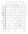
도 1은 실시형태 1에 있어서의 구동회로의 구성의 일례를 나타낸 회로도이다.
도 2는 도 1에 나타낸 구동회로의 동작을 나타낸 타이밍차트도이다.
도 3은 실시형태 1에 있어서의 구동회로의 구성의 일례를 나타낸 회로도이다.
도 4는 실시형태 1에 있어서의 구동회로의 구성의 일례를 나타낸 회로도이다.
도 5는 도 4에 나타낸 구동회로의 동작을 나타낸 타이밍차트도이다.
도 6은 실시형태 1에 있어서의 구동회로의 구성의 일례를 나타낸 회로도이다.
도 7은 실시형태 2에 있어서의 구동회로의 구성의 일례를 나타낸 회로도이다.
도 8은 도 7에 나타낸 구동회로의 동작을 나타낸 타이밍차트도이다.
도 9는 실시형태 2에 있어서의 구동회로의 구성의 일례를 나타낸 회로도이다.
도 10은 실시형태 2에 있어서의 구동회로의 구성의 일례를 나타낸 회로도이다.
도 11은 도 10에 나타낸 구동회로의 동작을 나타낸 타이밍차트도이다.
도 12는 실시형태 2에 있어서의 구동회로의 구성의 일례를 나타낸 회로도이다.
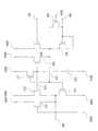
도 13은 실시형태 3에 있어서의 표시장치의 구성의 일례를 나타낸 회로도이다.
도 14는 도 13에 나타낸 주사선 구동회로 702의 동작을 나타낸 타이밍차트도이다.
도 15는 실시형태 3의 액정표시장치에 있어서의 화소의 구성 및 동작의 일례를 도시한 도면이다.
도 16은 실시형태 3의 액정표시장치에 있어서의 화소의 구성 및 동작의 일례를 도시한 도면이다.
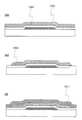
도 17은 실시형태 4에 있어서의 구동회로에 적용가능한 트랜지스터의 구성의 일례를 나타낸 단면 모식도이다.
도 18은 실시형태 4에 있어서의 구동회로에 적용가능한 트랜지스터의 구성의 일례를 나타낸 단면 모식도이다.
도 19는 실시형태 4에 있어서의 구동회로에 적용가능한 트랜지스터의 제조방법의 일례를 나타낸 단면 모식도이다.
도 20은 실시형태 4에 있어서의 구동회로에 적용가능한 트랜지스터의 제조방법의 일례를 나타낸 단면 모식도이다.
도 21은 실시형태 4에 있어서의 구동회로에 적용가능한 트랜지스터의 제조방법의 일례를 나타낸 단면 모식도이다.
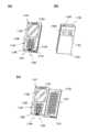
도 22는 실시형태 5에 있어서의 표시장치를 표시부에 적용가능한 전자기기의 일례를 도시한 도면이다.
도 23은 실시형태 5에 있어서의 표시장치를 표시부에 적용가능한 전자기기의 일례를 도시한 도면이다.
도 24는 실시형태 1에 있어서의 구동회로의 구성의 일례를 도시한 도면이다.
도 25는 실시형태 1에 있어서의 구동회로의 회로 계산 결과를 도시한 도면이다.1 is a circuit diagram showing an example of a configuration of a driving circuit according to the first embodiment.
FIG. 2 is a timing chart showing the operation of the driving circuit shown in FIG. 1.
3 is a circuit diagram showing an example of the configuration of a driving circuit in the first embodiment.
4 is a circuit diagram showing an example of the configuration of a driving circuit in the first embodiment.
5 is a timing chart showing the operation of the driving circuit shown in FIG. 4.
6 is a circuit diagram showing an example of the configuration of a driving circuit in the first embodiment.
7 is a circuit diagram showing an example of the configuration of a driving circuit in the second embodiment.
8 is a timing chart showing the operation of the driving circuit shown in FIG. 7.
9 is a circuit diagram showing an example of the configuration of a driving circuit in the second embodiment.
10 is a circuit diagram showing an example of the configuration of a driving circuit in the second embodiment.
11 is a timing chart showing the operation of the driving circuit shown in FIG. 10.
12 is a circuit diagram showing an example of the configuration of a driving circuit in the second embodiment.
13 is a circuit diagram showing an example of the configuration of a display device according to the third embodiment.
14 is a timing chart showing the operation of the scanning
15 is a diagram showing an example of a configuration and operation of a pixel in the liquid crystal display device according to the third embodiment.
16 is a diagram showing an example of a configuration and operation of a pixel in the liquid crystal display device according to the third embodiment.
17 is a schematic cross-sectional view showing an example of a configuration of a transistor applicable to a driving circuit in the fourth embodiment.
18 is a schematic cross-sectional view showing an example of a configuration of a transistor applicable to a driving circuit in the fourth embodiment.
19 is a schematic cross-sectional view showing an example of a method for manufacturing a transistor applicable to the driving circuit in the fourth embodiment.
20 is a schematic cross-sectional view showing an example of a method of manufacturing a transistor applicable to the driving circuit in the fourth embodiment.
Fig. 21 is a schematic cross-sectional view showing an example of a method for manufacturing a transistor applicable to the driving circuit in the fourth embodiment.
22 is a diagram showing an example of an electronic device to which the display device according to the fifth embodiment can be applied to a display unit.
23 is a diagram showing an example of an electronic device applicable to the display unit of the display device according to the fifth embodiment.
24 is a diagram showing an example of the configuration of a driving circuit in the first embodiment.
25 is a diagram showing a circuit calculation result of the driving circuit in the first embodiment.
본 발명의 실시형태의 예에 대해, 도면을 사용해서 이하에서 설명한다. 단, 본 발명은 이하의 설명에 한정되지 않고, 본 발명의 취지 및 그 범위에서 일탈하지 않고 그 형태 및 상세를 다양하게 변경할 수 있는 것은 당업자라면 용이하게 이해된다. 따라서, 본 발명은 이하에 나타낸 실시형태의 기재 내용에 한정해서 해석되는 것은 아닌 것으로 한다.An example of an embodiment of the present invention will be described below with reference to the drawings. However, the present invention is not limited to the following description, and it is readily understood by those skilled in the art that the form and detail can be variously changed without departing from the spirit and scope of the present invention. Therefore, the present invention is not intended to be interpreted as being limited to the description of the embodiments shown below.
(실시형태 1)(Embodiment 1)
본 실시형태에서는, 본 발명의 일 태양인 구동회로에 대해 설명한다.In this embodiment, a driving circuit that is an aspect of the present invention will be described.
본 실시형태에 있어서의 구동회로는, 복수의 플립플롭회로를 포함하는 시프트 레지스터를 갖는다.The driving circuit in this embodiment has a shift register including a plurality of flip-flop circuits.
더구나, 플립플롭회로의 회로 구성의 일례에 대해서 도 24를 사용하여 설명한다. 도 24는, 본 실시형태의 구동회로에 있어서의 플립플롭회로의 회로 구성의 일례를 나타낸 회로도이다.Further, an example of the circuit configuration of the flip-flop circuit will be described with reference to FIG. 24. 24 is a circuit diagram showing an example of a circuit configuration of a flip-flop circuit in the driving circuit of the present embodiment.
복수의 플립플롭회로의 적어도 한개는, 도 24에 나타낸 회로 구성의 플립플롭회로로 할 수 있다. 이때, 도 24에 나타낸 플립플롭회로는, 일례로서 제1 신호, 제2 신호, 및 제3 신호가 입력되고, 출력신호를 출력하는 기능을 갖는 것으로 한다.At least one of the plurality of flip-flop circuits can be a flip-flop circuit having the circuit configuration shown in FIG. 24. At this time, it is assumed that the flip-flop circuit shown in Fig. 24 has a function of inputting a first signal, a second signal, and a third signal and outputting an output signal as an example.
도 24에 나타낸 플립플롭회로는, 트랜지스터 11과, 트랜지스터 12와, 트랜지스터 13과, 트랜지스터 14, 트랜지스터 15를 갖는다.The flip-flop circuit shown in Fig. 24 includes
트랜지스터 11은, 게이트 단자에 제1 신호의 전위인 제1 전위가 주어지고, 소스 단자 및 드레인 단자의 한쪽에 제1 전위 또는 제2 전위가 주어진다.In the
트랜지스터 12는, 소스 단자 및 드레인 단자의 한쪽이 트랜지스터 11의 소스 단자 및 드레인 단자의 다른 쪽에 전기적으로 접속된다. 또한, 트랜지스터 12는, 게이트 단자에 제2 신호의 전위인 제3 전위가 주어지고, 소스 단자 및 드레인 단자의 다른 쪽에 제4 전위가 주어진다.In the
트랜지스터 13 및 트랜지스터 14는, 한쪽이 트랜지스터 11의 소스 단자 및 드레인 단자의 다른 쪽의 전위를 제1 전위 또는 제4 전위로 설정하는지 아닌지를 제어하는 기능을 갖고, 다른 쪽이 트랜지스터 11의 소스 단자 및 드레인 단자의 다른 쪽의 전위를 제4 전위로 설정하는지 아닌지를 제어하는 기능을 갖는다.
또한, 트랜지스터 13은, 트랜지스터 14가 온 상태일 때에 오프 상태가 되는 기능을 갖고, 또한, 트랜지스터 14는, 트랜지스터 13이 온 상태일 때에 오프 상태가 되는 기능을 갖는다.Further, the
트랜지스터 15는, 게이트 단자가 트랜지스터 11의 소스 단자 및 드레인 단자의 다른 쪽에 전기적으로 접속된다. 또한, 트랜지스터 15는, 소스 단자 및 드레인 단자의 한쪽에 제3 신호의 전위인 제5 전위가 주어지고, 소스 단자 및 드레인 단자의 다른 쪽의 전위가 출력신호의 전위가 된다. 이때, 트랜지스터 11의 소스 단자 및 드레인 단자의 다른 쪽과 트랜지스터 15의 게이트 단자의 접속 개소를 노드 A라고도 말한다.In the
또한, 트랜지스터 15는, 트랜지스터 13 또는 트랜지스터 14가 온 상태일 때 오프 상태이다.Further, the
상기한 구성에 의해, 트랜지스터 13 또는 트랜지스터 14가 온 상태일 때에는, 노드 A의 전위, 즉 트랜지스터 15의 게이트 단자의 전위가 소정의 값으로 설정되어, 노드 A가 부유 상태로 되지 않기 때문에, 플립플롭회로의 동작 불량을 억제 할 수 있다.With the above configuration, when the
더구나, 본 실시형태의 구동회로에 있어서의 플립플롭회로의 회로 구성의 일례에 대해 도 1을 사용하여 설명한다. 도 1은, 본 실시형태에 있어서의 플립플롭회로의 회로 구성의 일례를 나타낸 회로도이다.Further, an example of a circuit configuration of a flip-flop circuit in the driving circuit of the present embodiment will be described with reference to FIG. 1. 1 is a circuit diagram showing an example of a circuit configuration of a flip-flop circuit in the present embodiment.
본 실시형태의 구동회로에 있어서의 복수의 플립플롭회로의 각각은, 도 1에 나타낸 회로 구성의 플립플롭회로로 할 수 있다. 도 1에 나타낸 플립플롭회로는, 단자 100과, 단자 101과, 단자 102와, 단자 103과, 단자 104와, 단자 105와, 트랜지스터 106과, 트랜지스터 107과, 용량소자 108과, 트랜지스터 109와, 트랜지스터 110과, 트랜지스터 111과, 용량소자 112와, 트랜지스터 113과, 트랜지스터 114와, 트랜지스터 115와, 트랜지스터 116을 갖는다.Each of the plurality of flip-flop circuits in the driving circuit of the present embodiment can be a flip-flop circuit having the circuit configuration shown in FIG. 1. The flip-flop circuit shown in Fig. 1 includes a terminal 100, a terminal 101, a terminal 102, a terminal 103, a terminal 104, a terminal 105, a
이때, 도 1에 나타낸 플립플롭회로에서는, 단자 102로서 단자 102A 및 단자 102B를 보이고 있지만, 이것에 한정되지 않고, 본 실시형태의 구동회로에 있어서의 플립플롭회로에서는, 단자 102A 및 단자 102B를 전기적으로 접속시켜, 한개의 단자 102로 할 수도 있다. 또한, 도 1에 나타낸 플립플롭회로에서는, 단자 103으로서 단자 103A 및 단자 103B를 나타내고 있지만, 이것에 한정되지 않고, 본 실시형태의 구동회로에 있어서의 플립플롭회로에서는, 단자 103A 및 단자 103B를 전기적으로 접속시켜, 한개의 단자 103으로 할 수도 있다.At this time, in the flip-flop circuit shown in Fig. 1,
또한, 본 실시형태의 구동회로에 있어서의 플립플롭회로에서는, 단자 104로서 단자 104A 내지 단자 104G를 나타내고 있지만, 이것에 한정되지 않고, 본 실시형태의 구동회로에 있어서의 플립플롭회로에서는, 단자 104A 내지 단자 104G를 전기적으로 접속시켜, 한개의 단자 104로 할 수도 있다.In addition, in the flip-flop circuit in the driving circuit of the present embodiment,
트랜지스터106은, 게이트 단자가 단자 100에 전기적으로 접속되고, 소스 단자 및 드레인 단자의 한쪽이 트랜지스터 106의 게이트 단자에 전기적으로 접속된다.In the
트랜지스터 107은, 게이트 단자가 단자 101에 전기적으로 접속되고, 소스 단자 및 드레인 단자의 한쪽이 트랜지스터 106의 소스 단자 및 드레인 단자의 다른 쪽에 전기적으로 접속되고, 소스 단자 및 드레인 단자의 다른 쪽이 단자 104A에 전기적으로 접속된다. 이때, 편의를 위해 도시하지 않지만, 본 실시형태의 구동회로에 있어서의 플립플롭회로에 있어서, 트랜지스터 107을 설치하지 않는 구성으로 할 수도 있다. 트랜지스터 107을 설치하지 않는 구성으로 함으로써 회로 면적을 작게 할 수 있다.In the
용량소자 108은 적어도 2개의 단자를 갖고, 한쪽의 단자가 단자 102A에 전기적으로 접속된다.The
트랜지스터 109는, 게이트 단자가 트랜지스터 106의 소스 단자 및 드레인 단자의 한쪽에 전기적으로 접속되고, 소스 단자 및 드레인 단자의 한쪽이 용량소자 108의 다른 쪽의 단자에 전기적으로 접속되고, 소스 단자 및 드레인 단자의 다른 쪽이 단자 104B에 전기적으로 접속된다.In the
트랜지스터 110은, 게이트 단자가 트랜지스터 109의 소스 단자 및 드레인 단자의 한쪽에 전기적으로 접속되고, 소스 단자 및 드레인 단자의 한쪽이 트랜지스터 106의 소스 단자 및 드레인 단자의 다른 쪽에 전기적으로 접속되고, 소스 단자 및 드레인 단자의 다른 쪽이 단자 104C에 전기적으로 접속된다.In the
용량소자 112는 적어도 2개의 단자를 갖고, 한쪽의 단자가 단자 103A에 전기적으로 접속된다.The
트랜지스터 111은, 게이트 단자가 용량소자 112의 다른 쪽의 단자에 전기적으로 접속되고, 소스 단자 및 드레인 단자의 한쪽이 트랜지스터 106의 소스 단자 및 드레인 단자의 다른 쪽에 전기적으로 접속되고, 소스 단자 및 드레인 단자의 다른 쪽이 단자 104D에 전기적으로 접속된다.In the
트랜지스터 113은, 게이트 단자가 트랜지스터 106의 소스 단자 및 드레인 단자의 다른 쪽에 전기적으로 접속되고, 소스 단자 및 드레인 단자의 한쪽이 트랜지스터 111의 게이트 단자에 전기적으로 접속되고, 소스 단자 및 드레인 단자의 다른 쪽이 단자 104E에 전기적으로 접속된다.In the
트랜지스터 114는, 게이트 단자가 트랜지스터 106의 소스 단자 및 드레인 단자의 다른 쪽에 전기적으로 접속되고, 소스 단자 및 드레인 단자의 한쪽이 단자 103B에 전기적으로 접속되고, 소스 단자 및 드레인 단자의 다른 쪽이 단자 105에 전기적으로 접속되고, 소스 단자 및 드레인 단자의 다른 쪽의 전위가 출력신호가 되고, 단자 105를 거쳐 출력된다. 이때, 본 실시형태의 구동회로에 있어서의 플립플롭회로는, 트랜지스터 114의 게이트 단자와 소스 단자 및 드레인 단자의 다른 쪽과의 사이에 별도 용량소자를 설치하는 구성으로 할 수도 있다.In the
또한, 트랜지스터 115는, 게이트 단자가 트랜지스터 111의 게이트 단자에 전기적으로 접속되고, 소스 단자 및 드레인 단자의 한쪽이 트랜지스터 114의 소스 단자 및 드레인 단자의 다른 쪽에 전기적으로 접속되고, 소스 단자 및 드레인 단자의 다른 쪽이 단자 104F에 전기적으로 접속된다.In addition, in the
또한, 트랜지스터 116은, 게이트 단자가 단자 102B에 전기적으로 접속되고, 소스 단자 및 드레인 단자의 한쪽이 트랜지스터 114의 소스 단자 및 드레인 단자의 다른 쪽에 전기적으로 접속되고, 소스 단자 및 드레인 단자의 다른 쪽이 단자 104G에 전기적으로 접속된다.In addition, in the
이때, 트랜지스터 109의 소스 단자 및 드레인 단자의 한쪽과, 용량소자 108의 다른 쪽의 단자 또는 트랜지스터 110의 게이트 단자의 접속 개소를 노드 118이라고도 말한다. 또한, 트랜지스터 106의 소스 단자 및 드레인 단자의 다른 쪽과, 트랜지스터 107의 소스 단자 및 드레인 단자의 한쪽, 트랜지스터 110의 소스 단자 및 드레인 단자의 한쪽, 트랜지스터 111의 소스 단자 및 드레인 단자의 한쪽, 트랜지스터 113의 게이트 단자, 또는 트랜지스터 114의 게이트 단자와의 접속 개소를 노드 117이라고도 말한다. 또한, 트랜지스터 111의 게이트 단자와, 용량소자 112의 다른 쪽의 단자, 트랜지스터 113의 소스 단자 및 드레인 단자의 한쪽, 또는 트랜지스터 115의 게이트 단자와의 접속 개소를 노드 119라고도 한다.At this time, a connection point between one of the source and drain terminals of the
또한, 도 1에 나타낸 플립플롭회로는, 단자 100을 통해 제1 제어신호가 입력되고, 단자 101을 통해 제2 제어신호가 입력된다. 제1 제어신호 및 제2 제어신호는, 예를 들면 각각 하이 상태와 로우 상태의 2개의 상태를 갖는 디지털 신호를 사용할 수 있다. 디지털 신호를 사용하는 경우, 입력되는 제1 제어신호 또는 제2 제어신호가 하이 상태일 때(하이레벨이라고도 한다)에는, 단자 100 또는 단자 101을 거쳐 제1 전위(V1이라고도 한다)로서 소정의 값의 전위인 제1 제어신호 또는 제2 제어신호가 입력되고, 입력되는 제1 제어신호 또는 제2 제어신호가 로우 상태일 때(로우 레벨이라고도 한다)에는, 단자 100 또는 단자 101을 거쳐 제2 전위(V2라고도 한다)로서 상기 하이 상태에 있어서의 소정의 값의 전위보다 낮은 값의 전위인 제1 제어신호 또는 제2 제어신호가 입력된다. 하이 상태 및 로우 상태에 있어서의 전위의 값은, 예를 들면 트랜지스터의 임계전압의 값 등을 고려해서 적당하게 설정할 수 있다. 예를 들면, 하이 상태와 로우 상태의 전위차가 플립플롭회로 내의 트랜지스터의 임계전압의 절대값보다 커지도록, 하이 상태 및 로우 상태에 있어서의 전위의 값을 설정하는 것이 바람직하다.Further, in the flip-flop circuit shown in FIG. 1, a first control signal is input through a terminal 100, and a second control signal is input through a terminal 101. As the first control signal and the second control signal, for example, a digital signal having two states of a high state and a low state may be used. In the case of using a digital signal, when the input first control signal or the second control signal is in a high state (also referred to as a high level), a predetermined value as a first potential (also referred to as V1) via a terminal 100 or a terminal 101 When a first control signal or a second control signal that is a potential of is input, and the input first control signal or second control signal is in a low state (also referred to as a low level), the second potential is passed through the terminal 100 or the terminal 101. As (also referred to as V2), a first control signal or a second control signal, which is a potential lower than a potential of a predetermined value in the high state, is input. The value of the potential in the high state and the low state can be appropriately set in consideration of, for example, the value of the threshold voltage of the transistor. For example, it is preferable to set the potential values in the high state and the low state so that the potential difference between the high state and the low state is greater than the absolute value of the threshold voltage of the transistor in the flip-flop circuit.
또한, 도 1에 나타낸 플립플롭회로는, 단자 102(단자 102A 및 단자 102B라고도 한다)를 거쳐 제1 위상인 클록신호(제1 클록신호, 또는 CK 신호라고도 한다) 또는 제2 위상인 클록신호(제2 클록신호, CKB 신호, 또는 제1 클록신호의 반전 신호라고도 한다)가 입력된다. 제1 클록신호 및 제2 클록신호는, 하이 상태와 로우 상태의 2개의 전위의 상태를 갖고, 하이 상태일 때(하이레벨이라고도 한다)에는, 클록신호의 전위가 전위 V1이 되고, 로우 상태일 때(로우 레벨이라고도 한다)에는, 클록신호의 전위가 전위 V2가 된다. 이때, 하이 상태일 때의 제1 클록신호 및 제2 클록신호의 전위는, 하이 상태일 때의 제1 제어신호 및 제2 제어신호의 전위와 동등한 값인 것이 바람직하며, 로우 상태일 때의 제1 클록신호 및 제2 클록신호의 전위는, 로우 상태일 때의 제1 제어신호 및 제2 제어신호의 전위와 동등한 값인 것이 바람직하다. 또한, 하이 상태 및 로우 상태에 있어서의 전위의 값은, 예를 들면 트랜지스터의 임계전압의 값 등을 고려해서 적당하게 설정할 수 있다. 예를 들면, 하이 상태와 로우 상태의 전위차가 플립플롭회로 내의 트랜지스터의 임계전압의 절대값보다 커지도록, 하이 상태 및 로우 상태에 있어서의 전위의 값을 설정하는 것이 바람직하다.In addition, the flip-flop circuit shown in Fig. 1 is a clock signal (also referred to as a first clock signal or a CK signal) or a clock signal (also referred to as a first clock signal or a CK signal) as a first phase via a terminal 102 (also referred to as a terminal 102A and a terminal 102B). A second clock signal, a CKB signal, or an inverted signal of the first clock signal) is input. The first clock signal and the second clock signal have two potential states, a high state and a low state, and when in a high state (also referred to as a high level), the potential of the clock signal becomes a potential V1 and is in a low state. At this time (also referred to as the low level), the potential of the clock signal becomes the potential V2. In this case, the potentials of the first clock signal and the second clock signal in the high state are preferably equal to the potentials of the first control signal and the second control signal in the high state, and the first clock signal in the low state It is preferable that the potentials of the clock signal and the second clock signal are equal to the potentials of the first control signal and the second control signal in the low state. Further, the value of the potential in the high state and the low state can be appropriately set in consideration of, for example, the value of the threshold voltage of the transistor. For example, it is preferable to set the potential values in the high state and the low state so that the potential difference between the high state and the low state is greater than the absolute value of the threshold voltage of the transistor in the flip-flop circuit.
제1 클록신호와 제2 클록신호의 2개의 클록신호는, 위상이 상반된 관계로서, 예를 들면, 소정의 기간에 있어서, 제1 클록신호가 하이 상태일 때에는, 제2 클록신호는 로우 상태이며, 제1 클록신호가 로우 상태일 때에는, 제2 클록신호는 하이 상태이다.The two clock signals of the first clock signal and the second clock signal are in a phase-inverted relationship. For example, in a predetermined period, when the first clock signal is in a high state, the second clock signal is in a low state. , When the first clock signal is in a low state, the second clock signal is in a high state.
또한, 플립플롭회로는, 단자 103(단자 103A 및 단자 103B라고도 한다)을 거쳐 제1 클록신호 또는 제2 클록신호가 입력된다. 이때, 단자 102를 거쳐 입력되는 클록신호와 단자 103을 거쳐 입력되는 클록신호는 상반된 관계로서, 예를 들면, 단자 102를 통해 제1 클록신호가 입력될 경우에는, 단자 103을 통해 제2 클록신호가 입력되고, 단자 102를 통해 제2 클록신호가 입력될 경우에는, 단자 103을 통해 제1 클록신호가 입력된다.Further, to the flip-flop circuit, the first clock signal or the second clock signal is input through the terminal 103 (also referred to as terminal 103A and terminal 103B). At this time, the clock signal input through the terminal 102 and the clock signal input through the terminal 103 are in an opposite relationship. For example, when the first clock signal is input through the terminal 102, the second clock signal through the terminal 103 When is input and the second clock signal is input through the terminal 102, the first clock signal is input through the terminal 103.
또한, 도 1에 나타낸 플립플롭회로는, 단자 104(단자 104A 내지 단자 104G라고도 한다)를 거쳐 소정의 값의 전위가 주어진다. 이때, 소정의 값의 전위의 값은, 예를 들면, V1 또는 V2로 할 수 있고, 즉 클록신호 또는 제어신호 등의 디지털 신호의 하이 상태 또는 로우 상태에 있어서의 전위의 값과 동등한 값으로 할 수 있다.Further, in the flip-flop circuit shown in Fig. 1, a potential of a predetermined value is given through a terminal 104 (also referred to as a terminal 104A to a terminal 104G). At this time, the value of the potential of a predetermined value can be, for example, V1 or V2, that is, a value equal to the value of the potential in the high or low state of a digital signal such as a clock signal or a control signal. I can.
이때, 도 1에 나타낸 플립플롭회로에 있어서, 트랜지스터 106의 소스 단자 및 드레인 단자의 한쪽이 단자 100에 전기적으로 접속되는 구성에 대해 설명했지만, 이것에 한정되지 않고, 본 실시형태의 구동회로에 있어서의 플립플롭회로는, 별도의 전원단자에 전기적으로 접속된 구성으로 하여, 전위 V1 또는 전위 V2가 주어지는 구성으로 할 수도 있다.At this time, in the flip-flop circuit shown in Fig. 1, a configuration in which one of the source terminal and the drain terminal of the
트랜지스터 106은, 단자 100을 통해 입력되는 신호에 따라, 단자 100과 노드 117의 도통을 제어하는 기능을 갖는다.The
트랜지스터 107은, 단자 101을 통해 입력되는 신호에 따라, 단자 104A와 노드 117의 도통을 제어하는 기능을 갖고, 단자 104A와 노드 117이 도통상태가 됨으로써, 노드 117의 전위가 V1 또는 V2로 설정된다.
용량소자 108은, 단자 102(단자 102A)를 거쳐 입력되는 신호에 따라서, 용량결합에 의해 노드 118의 전위를 변동시키는 기능을 갖는다. 예를 들면, 단자 102(단자 102A)를 거쳐 입력되는 신호가 로우 상태로부터 하이 상태가 되었을 경우, 용량소자 108은, 용량결합에 의해 노드 118의 전위를 전위 V1으로 설정하는 기능을 갖는다. 한편, 단자 102를 통해 입력되는 신호가 하이 상태로부터 로우 상태가 되었을 경우, 용량소자 108은, 용량결합에 의해 노드 118의 전위를 V1 또는 V2로 설정하는 기능을 갖는다.The
트랜지스터 109는, 단자 100을 통해 입력되는 신호에 따라서, 단자 104B와 노드 118의 도통을 제어하는 기능을 갖고, 단자 104B와 노드118이 도통상태가 됨으로써 노드118의 전위가 V1 또는 V2로 설정된다.The
트랜지스터 110은, 노드 118의 전위에 따라, 단자 104C와 노드 117의 도통을 제어하는 기능을 갖고, 단자 104C와 노드 117이 도통상태가 됨으로써 노드 117의 전위가 V1 또는 V2로 설정된다. 또한, 트랜지스터 110은, 트랜지스터 111이 온 상태일 때에 오프 상태가 되는 기능을 갖는다.The
트랜지스터 111은, 노드 119의 전위에 따라서, 단자 104D와 노드 117의 도통을 제어하는 기능을 갖고, 단자 104D와 노드 117이 도통상태가 됨으로써 노드 117의 전위가 V1 또는 V2로 설정된다. 또한, 트랜지스터 111은, 트랜지스터 110이 온 상태일 때에 오프 상태가 되는 기능을 갖는다.The
용량소자 112는, 단자 103A를 거쳐 입력되는 신호에 따라서, 용량결합에 의해 노드 119의 전위를 변동시키는 기능을 갖는다. 예를 들면, 단자 103A를 거쳐 입력되는 신호가 로우 상태로부터 하이 상태가 되었을 경우, 용량소자 112는, 용량결합에 의해 노드 119의 전위를 V1로 설정한다. 한편, 단자 103A를 거쳐 입력되는 신호가 하이 상태로부터 로우 상태가 되었을 경우, 용량소자 112는, 용량결합에 의해 노드 119의 전위를 V2로 설정한다.The
트랜지스터 113은, 단자 104E와 노드 119의 도통을 제어하는 기능을 갖고, 단자 104E와 노드 119가 도통상태가 됨으로써 노드 119의 전위가 V1 또는 V2로 설정된다.The
트랜지스터 114는, 노드 117의 전위에 따라서, 단자 103B와 단자 105의 도통을 제어하고, 단자 103B와 단자 105가 도통상태가 되는 것에 의해, 단자 103B를 거쳐 입력되는 신호의 전위와 단자 105를 통해 출력되는 신호의 전위를 동등한 값으로 하는 기능을 갖는다.The
또한, 트랜지스터 114는, 예를 들면, N형 트랜지스터로서 노드 117의 전위가 V1인 경우에, 단자 103B를 거쳐 입력되는 신호가 로우 상태로부터 하이 상태로 변화하면, 단자 105와의 접속 개소의 전위의 상승에 따라서 노드 117의 전위를 상승시키는 기능을 갖는다. 소위, 부트스트랩이다. 단, 부트스트랩은, 트랜지스터 114의 게이트 단자와, 소스 단자 및 드레인 단자의 다른 쪽과의 사이의 기생 용량에 의해 행해지는 일이 많다.In addition, when the potential of the
트랜지스터 115는, 노드 119의 전위에 따라서, 단자 104F와 단자 105의 도통을 제어하는 기능을 갖고, 단자 104F와 단자 105가 도통상태가 되는 것에 의해, 단자 105를 통해 출력하는 신호의 전위가 V1 또는 V2로 설정된다.
트랜지스터 116은, 단자 102B를 거쳐 입력되는 신호에 따라서, 단자 104G와 단자 105의 도통을 제어하는 기능을 갖고, 단자 104G와 단자 105를 도통상태로 하여, 단자 105를 통해 출력되는 신호의 전위를 V1 또는 V2로 설정하는 기능을 갖는다.
이때, 본 실시형태에 있어서의 구동회로는, 모두 동일한 도전형의 트랜지스터에 의해 구성할 수 있으므로, 제조공정의 간략화를 도모할 수 있다. 따라서, 제조비용의 삭감이나 제품 수율의 향상을 도모할 수 있다. 더구나, 대형의 표시 패널 등의 반도체장치를 제조하는 것도 용이하게 된다. 본 실시형태의 구동회로에서는, 모든 트랜지스터를 N형의 도전형의 트랜지스터(N형 트랜지스터라고도 한다) 또는 P형의 도전형의 트랜지스터(P형 트랜지스터라고도 한다)로 할 수도 있다. 이때, 본 명세서에 있어서 동일이란 실질적으로 동일한 것도 포함된다.At this time, since the drive circuits in the present embodiment can all be configured by transistors of the same conductivity type, the manufacturing process can be simplified. Therefore, it is possible to reduce the manufacturing cost and improve the product yield. Moreover, it becomes easy to manufacture a semiconductor device such as a large-sized display panel. In the driving circuit of this embodiment, all transistors may be N-type conductivity type transistors (also referred to as N-type transistors) or P-type conductivity type transistors (also referred to as P-type transistors). In this case, the same in the present specification includes substantially the same thing.
다음에, 도 1에 나타낸 구동회로의 동작에 대해 도 2를 사용하여 설명한다. 도 2는, 도 1에 나타낸 구동회로의 동작의 일례를 나타낸 타이밍차트이다. 이때, 본 실시형태에서는, 일례로서, 단자 102를 통해 제2 클록신호가 입력되고, 단자 103을 통해 제1 클록신호가 입력되는 것으로 한다. 또한, 여기에서는, 도 1에 나타낸 구동회로의 동작의 일례로서 플립플롭회로 내의 트랜지스터가 모두 N형 트랜지스터인 경우에 대해 설명한다.Next, the operation of the driving circuit shown in FIG. 1 will be described with reference to FIG. 2. 2 is a timing chart showing an example of the operation of the driving circuit shown in FIG. 1. At this time, in the present embodiment, as an example, it is assumed that the second clock signal is input through the terminal 102 and the first clock signal is input through the terminal 103. In addition, here, as an example of the operation of the driving circuit shown in Fig. 1, a case where all the transistors in the flip-flop circuit are N-type transistors will be described.
도 1에 나타낸 구동회로의 동작은, 도 2에 나타낸 것과 같이, 일정한 기간에 있어서의 소정의 동작이 반복하여 행해진다. 일정한 기간은, 주로 선택 기간과 비선택 기간으로 나뉘며, 다시 선택 기간 및 비선택 기간은 제1 기간, 제2 기간, 제3 기간, 제4 기간, 및 제5 기간으로 나뉘어진다. 도 2에 있어서, 제1 기간, 제3 기간, 제4 기간, 및 제5 기간은 비선택 기간이며, 제2 기간은 선택 기간이다.In the operation of the driving circuit shown in FIG. 1, as shown in FIG. 2, a predetermined operation in a certain period is repeatedly performed. The certain period is mainly divided into a selected period and a non-selected period, and again, the selected period and the non-selected period are divided into a first period, a second period, a third period, a fourth period, and a fifth period. In Fig. 2, the first period, the third period, the fourth period, and the fifth period are non-selection periods, and the second period is a selection period.
우선, 제1 기간에서는, 단자 100을 통해 하이 상태인 제1 제어신호 201이 입력되고, 단자 101을 통해 로우 상태인 제2 제어신호 208이 입력되고, 단자 102를 통해 하이 상태인 제2 클록신호 203이 입력되고, 단자 103을 통해 로우 상태인 제1 클록신호 202가 입력됨으로써, 트랜지스터 106, 트랜지스터 109, 및 트랜지스터 116이 온 상태가 되고, 트랜지스터 107이 오프 상태가 된다.First, in the first period, a
트랜지스터 106이 온 상태가 되면 노드 117의 전위 204가 상승하기 시작한다. 이때, 노드 117의 전위는, 제1 제어신호 201의 전위 V1으로부터 트랜지스터 106의 임계전압(Vth106이라고도 한다)을 뺀 값, 즉 V1-Vth106이 될 때까지 상승하여, V1-Vth106이 되면 트랜지스터 106은 오프 상태가 된다.When the
더구나, 노드 117의 전위 204가 V1-Vth106이 되면, 트랜지스터 113은 온 상태가 된다. 이때, 노드 119의 전위 206은, 단자 104E를 거쳐 주어지는 전위 V2와 동등한 값이 된다.Furthermore, when the potential 204 of the
더구나, 노드 119의 전위 206이 V2가 되면, 트랜지스터 111 및 트랜지스터 115는 오프 상태가 된다.Furthermore, when the potential 206 of the
또한, 트랜지스터 109가 온 상태가 되면, 노드 118의 전위 205는, 단자 104B를 거쳐 주어지는 전위 V2와 동등한 값이 된다.Further, when the
더구나, 노드 118의 전위 205가 V2가 되면, 트랜지스터 110이 오프 상태가 된다.Furthermore, when the potential 205 of the
더구나, 상기한 것과 같이, 트랜지스터 106, 트랜지스터 107, 트랜지스터 110, 및 트랜지스터 111이 오프 상태가 되면, 노드 117은, 전위가 V1-Vth106으로 유지된 채 부유 상태가 된다.Further, as described above, when the
또한, 노드 117의 전위 204가 V1-Vth106이 되면, 트랜지스터 114가 온 상태가 된다.Further, when the potential 204 of the
더구나, 이때 단자 105를 통해 출력되는 출력신호 207의 전위는, 단자 103B를 거쳐 주어지는 전위 V2, 또는 단자 104G를 거쳐 주어지는 전위 V2와 동등한 값이 된다. 이상이 제1 기간에 있어서의 동작이다.In addition, the potential of the
다음에 제2 기간에서는, 단자 100을 통해 로우 상태인 제1 제어신호 201이 입력되고, 단자 101을 통해 로우 상태인 제2 제어신호 208이 입력되고, 단자 102를 통해 로우 상태인 제2 클록신호 203이 입력되고, 단자 103을 통해 하이 상태인 제1 클록신호 202가 입력된다. 이때, 트랜지스터 106, 트랜지스터 109, 및 트랜지스터 116이 오프 상태가 되고, 트랜지스터 107은 오프 상태 그대로이다.Next, in the second period, the
이때, 트랜지스터 109는, 단자 102A를 거쳐 입력되는 제2 클록신호 203이 로우 상태가 된 후에 오프 상태가 되는 경우가 많다. 왜냐하면 단자 100을 통해 입력되는 제1 제어신호 201은 제2 클록신호 203보다도 지연되어 있는 경우가 많기 때문이다. 제2 클록신호 203이 로우 상태가 된 후에 트랜지스터 109가 오프 상태가 되는 것에 의해, 노드 118은, 전위 V2로 유지된 채 부유 상태가 되고, 트랜지스터 110은 오프 상태 그대로이다.At this time, the
또한, 용량소자 108에는, 단자 102A를 거쳐 입력되는 제2 클록신호 203의 전위와 노드 118의 전위 205의 전위차, 즉 로우 상태인 제2 클록신호 203의 전위와, 단자 104B를 거쳐 주어지는 전위 V2의 전위차가 유지된다.Further, in the
또한, 상기한 것과 같이 트랜지스터 106, 트랜지스터 107, 및 트랜지스터 110이 오프 상태일 때, 노드 117의 전위 204가 V1-Vth106인 채이다.Further, as described above, when the
더구나, 노드 117의 전위 204가 V1-Vth106일 때, 트랜지스터 113은 온 상태 그대로이며, 트랜지스터 113이 온 상태 그대로일 때, 노드 119의 전위 206은 V2인 채이며, 트랜지스터 111 및 트랜지스터 115는 오프 상태 그대로이다.In addition, when the potential 204 of the
노드 117의 전위 204가 V1-Vth106인 채로서, 트랜지스터 114의 소스 단자 및 드레인 단자의 한쪽의 전위가 제1 클록신호 202의 전위 V1이 되면, 단자 105를 통해 출력되는 출력신호 207의 전위가 상승한다. 그러면 노드 117은 부유 상태이기 때문에, 노드 117의 전위 204는, 트랜지스터 114의 게이트 단자와, 소스 단자 및 드레인 단자의 다른 쪽과의 사이의 기생 용량에 의한 용량결합에 의해, 출력신호 207의 전위에 맞춰서 상승한다. 소위 부트스트랩이다.When the potential 204 of the
노드 117의 전위 204는, 제1 클록신호 202의 전위 V1과, 트랜지스터 114의 임계전압(Nth114라고도 한다)과의 합보다도 더 큰 값, 즉 V1+Vth114+Va(Va는 임의의 양의 값)까지 상승한다. 이때, 트랜지스터 114는 온 상태 그대로이다.The potential 204 of the
더구나, 이때 단자 105를 통해 출력되는 출력신호 207의 전위는, 단자 103B를 거쳐 주어지는 전위 V1과 동등한 값이 된다. 이상이 제2 기간에 있어서의 동작이다.Moreover, at this time, the potential of the
다음에 제3 기간에서는, 단자 100을 통해 로우 상태인 제1 제어신호 201이 입력되고, 단자 101을 통해 하이 상태인 제2 제어신호 208이 입력되고, 단자 102를 통해 하이 상태인 제2 클록신호 203이 입력되고, 단자 103을 통해 로우 상태인 제1 클록신호 202가 입력된다. 이때, 트랜지스터 107 및 트랜지스터 116이 온 상태가 되고, 트랜지스터 106 및 트랜지스터 109가 오프 상태 그대로이다.Next, in the third period, the
트랜지스터 107이 온 상태가 되면, 노드 117의 전위 204가 단자 104A를 거쳐 주어지는 전위 V2와 동등한 값이 된다.When the
더구나, 노드 118의 전위 205는, 용량소자 108의 용량결합에 의해 V2+Vb가 된다. Vb은, 트랜지스터 110의 임계전압보다도 큰 것이 바람직하며, V1-V2보다도 작은 것이 바람직하다.In addition, the potential 205 of the
더구나, 노드 118의 전위 205의 전위가 V2+Vb이 되면 트랜지스터 110이 온 상태가 된다. 더구나, 트랜지스터 110이 온 상태가 되면 노드 117의 전위 204가 단자 104C를 거쳐 주어지는 전위 V2와 동등한 값이 된다.Furthermore, when the potential of the potential 205 of the
더구나, 노드 117의 전위 204가 전위 V2가 되면 트랜지스터 113 및 트랜지스터 114가 오프 상태가 된다. 이때, 트랜지스터 113은, 단자 103A를 거쳐 입력되는 제1 클록신호 202가 로우 상태가 된 후에 오프 상태가 되는 경우가 많다. 왜냐하면, 노드 117의 전위 204는, 제1 클록신호 202보다도 지연 또는 둔해지고 있는 경우가 많기 때문이다. 제1 클록신호 202가 로우 상태가 된 후에 트랜지스터 113이 오프 상태가 되면, 단자 104E를 거쳐 주어지는 전위 V2와 동등한 값이 유지된 채 노드 119가 부유 상태가 된다.Furthermore, when the potential 204 of the
더구나, 노드 119가 부유 상태일 때, 트랜지스터 111 및 트랜지스터 115가 오프 상태 그대로이다.Moreover, when the
더구나, 용량소자 112에는, 단자 103A를 거쳐 입력되는 제1 클록신호 202의 전위와, 노드 119의 전위 206의 전위차, 즉 로우 상태인 제1 클록신호 202의 전위와, 단자 104E를 거쳐 주어지는 전위 V2의 전위차가 유지된다.In addition, to the
더구나, 이때 단자 105를 통해 출력되는 출력신호 207의 전위는, 단자 104G를 거쳐 주어지는 전위 V2와 동등한 값이 된다. 이상이 제3 기간에 있어서의 동작이다.Moreover, at this time, the potential of the
다음에, 제4 기간에서는, 단자 100을 통해 로우 상태인 제1 제어신호 201이 입력되고, 단자 101을 통해 로우 상태인 제2 제어신호 208이 입력되고, 단자 102를 통해 로우 상태인 제2 클록신호 203이 입력되고, 단자 103을 통해 하이 상태인 제1 클록신호 202가 입력된다. 이때, 트랜지스터 107 및 트랜지스터 116이 오프 상태가 되고, 트랜지스터 106 및 트랜지스터 109는 오프 상태 그대로이다.Next, in the fourth period, the
이때, 노드 118의 전위 205는, 용량소자 108의 용량결합에 의해 V2가 된다. 따라서, 트랜지스터 110은 오프 상태가 된다.At this time, the potential 205 of the
또한, 노드 119의 전위 206은, 용량소자 112의 용량결합에 의해 V2+Vc가 된다. Vc은 트랜지스터 111의 임계전압 또는 트랜지스터 115의 임계전압보다도 큰 것이 바람직하며, V1-V2보다도 작은 것이 바람직하다.Further, the potential 206 of the
더구나, 노드 119의 전위 206이 V2+Vc가 되면, 트랜지스터 111 및 트랜지스터 115가 온 상태가 된다.Furthermore, when the potential 206 of the
더구나, 트랜지스터 111이 온 상태가 되면, 노드 117의 전위 204가 단자 104D를 거쳐 주어지는 전위 V2와 동등한 값이 된다.Furthermore, when the
더구나, 노드 117의 전위 204가 V2가 되면, 트랜지스터 113 및 트랜지스터 114가 오프 상태가 된다.Furthermore, when the potential 204 of the
또한, 트랜지스터 115가 온 상태가 되면, 단자 105를 통해 출력되는 출력신호 207의 전위는, 단자 104F를 거쳐 주어지는 전위 V2와 동등한 값이 된다. 이상이 제4 기간에 있어서의 동작이다.Further, when the
다음에, 제5 기간에서는, 단자 100을 통해 로우 상태인 제1 제어신호 201이 입력되고, 단자 101을 통해 로우 상태인 제2 제어신호 208이 입력되고, 단자 102를 통해 하이 상태인 제2 클록신호 203이 입력되고, 단자 103을 통해 로우 상태인 제1 클록신호 202가 입력된다. 이때 트랜지스터 116이 온 상태가 되고, 트랜지스터 106, 트랜지스터 107, 및 트랜지스터 109는 오프 상태 그대로이다.Next, in the fifth period, the
이때 노드 118의 전위는 용량소자 108의 용량결합에 의해 V2+Vb이 된다. 더구나, 노드 118의 전위가 V2+Vb이 되면, 트랜지스터 110이 온 상태가 된다. 더구나, 트랜지스터 110이 온 상태가 되면, 노드 117의 전위 204가 단자 104C를 거쳐 주어지는 전위 V2와 동등한 값이 된다.At this time, the potential of the
또한, 노드 119의 전위 206은, 용량소자 112의 용량결합에 의해 V2가 된다. 더구나, 노드 119의 전위 206이 V2가 되면, 트랜지스터 111 및 트랜지스터 115는 오프 상태가 된다.Further, the potential 206 of the
더구나, 노드 117의 전위 204가 V2가 되면, 트랜지스터 113 및 트랜지스터 114가 오프 상태가 된다.Furthermore, when the potential 204 of the
더구나, 이때 단자 105를 통해 출력되는 출력신호 207의 전위는, 단자 104G를 거쳐 주어지는 전위 V2와 동등한 값이 된다. 이상이 제5 기간에 있어서의 동작이다.Moreover, at this time, the potential of the
이상과 같이, 본 실시형태에 있어서의 구동회로는, 리셋트 기간(제3 기간) 후의 비선택 기간의 사이, 제4 기간 및 제5 기간의 동작이 복수회 반복 행해진다. 이에 따라 비선택 기간의 어느쪽의 기간에 있어서도 노드 117에 소정의 값의 전위가 주어지기 때문에, 117이 부유 상태가 되는 것을 억제할 수 있다. 따라서 노이즈에 의한 영향을 저감할 수 있으므로, 동작 불량을 억제할 수 있다.As described above, in the driving circuit according to the present embodiment, the operations of the fourth period and the fifth period are repeatedly performed a plurality of times during the non-selection period after the reset period (third period). Accordingly, since a potential of a predetermined value is given to the
또한, 본 실시형태에 있어서의 구동회로의 동작에 있어서, 제4 기간과, 제5 기간에서 다른 트랜지스터를 온 상태에 함으로써 노드 117에 소정의 값의 전위를 줄 수 있기 때문에, 예를 들면, 반도체층이 비정질 반도체인 트랜지스터 등, 열화하기 쉬운 트랜지스터를 적용했을 경우에 있어서도 각 트랜지스터에 있어서의 열화를 억제할 수 있다. 따라서 열화에 의한 트랜지스터의 스위칭 동작의 타이밍의 불일치를 저감할 수 있으므로, 동작 불량을 억제할 수 있다.In addition, in the operation of the driving circuit in this embodiment, a potential of a predetermined value can be given to the
여기에서 도 2에 나타낸 제4 기간과 제5 기간에 있어서, 트랜지스터 110 및 트랜지스터 111의 한쪽의 트랜지스터만을 설치해서 노드 117의 전위를 제어하는 종래의 구동회로의 경우와, 트랜지스터 110 및 트랜지스터 111의 양쪽의 트랜지스터를 설치해서 노드 117의 전위를 제어하는 본 발명의 일 태양인 구동회로의 경우의 회로 계산 결과를 도 25에 나타낸다. 이때, 계산은 SPICE 회로 시뮬레이터를 사용하여 행하였다. 또한, 여기에서는 일례로서 플립플롭회로 내의 트랜지스터를 모두 N형 트랜지스터로 하고, V2=0V로 하였다.Here, in the fourth and fifth periods shown in Fig. 2, in the case of a conventional driving circuit in which only one of the
도 25 중에서, 도 25a는, 제4 기간과 제5 기간에 있어서, 트랜지스터 110 및 트랜지스터 111의 한쪽의 트랜지스터를 사용해서 노드 117을 제어하는 경우에 있어서의 노드 117의 전위(전압)의 변화를 나타낸 도면이고, 도 25b는, 제4 기간과 제5 기간에 있어서, 트랜지스터 110 및 트랜지스터 111의 양쪽의 트랜지스터를 사용해서 노드 117을 제어하는 경우에 있어서의 노드 117의 전위(전압)의 변화를 도시한 도면이다. 이때, 도 25a 및 도 25b에 있어서, 전압의 단위는, 임의 단위(A.U.: Arbitrary Unit)로 한다.In FIG. 25, FIG. 25A shows the change in the potential (voltage) of the
리셋트 기간후의 제4 기간 및 제5 기간에 있어서 발생하는 노이즈는, 주로 도 1에 나타낸 트랜지스터 114의 기생 용량에 의해 노드 117에 영향을 미친다. 우선 종래의 구동회로에서는, 한개의 클록신호에 동기한 신호를 사용해서 트랜지스터를 제어하기 때문에, 리셋트 기간후, 제4 기간 및 제5 기간 어느 쪽인가 한쪽의 기간에서 부유 상태가 된다. 부유 상태가 되면 일반적인 전위에 노이즈가 합쳐, 도 25a에 나타낸 것과 같이 일정한 기간(도 25a에서는 제5 기간)마다 노드 117의 전위(전압)가 0.4 정도 변동해 버린다.Noise generated in the fourth and fifth periods after the reset period mainly affects the
한편, 본 발명의 일 태양인 구동회로에서는, 위상이 상반된 관계인 2개의 클록신호의 각각에 동기한 신호를 사용해서 트랜지스터 110 및 트랜지스터 111을 제어하기 때문에, 제4 기간 및 제5 기간의 양쪽의 기간에서 부유 상태가 되지 않고 소정의 전위가 주어지기 때문에, 도 25b에 나타낸 것과 같이, 노드 117의 전위의 변화가 0.2 이하로 변동이 적은, 즉 노이즈의 영향이 적은 것을 알 수 있다. 이상의 내용으로부터 복수의 트랜지스터를 사용하여, 제4 기간 및 제5 기간의 각 기간에 트랜지스터 110 또는 트랜지스터 111을 온 상태로 함으로써 노드 117에 소정의 값의 전위를 주는 것에 의해 노이즈에 의한 영향을 저감할 수 있다는 것을 알 수 있다.On the other hand, in the driving circuit, which is an aspect of the present invention, since the
더구나, 본 실시형태에서는, 도 1과 다른 구성을 사용해서 본 발명의 일 태양인 구동회로로 할 수도 있다. 본 실시형태에 있어서의 구동회로의 다른 구성에 대해서 도 3을 사용하여 설명한다. 도 3은, 본 실시형태의 구동회로의 구성의 일례를 나타낸 회로도이다.In addition, in this embodiment, a configuration different from that of Fig. 1 can be used to obtain a driving circuit, which is an aspect of the present invention. Another configuration of the drive circuit in this embodiment will be described with reference to FIG. 3. 3 is a circuit diagram showing an example of the configuration of the driving circuit of the present embodiment.
도 3에 나타낸 본 실시형태에 있어서의 구동회로의 다른 구성은, 도 1에 나타낸 회로 구성에 덧붙여, 트랜지스터 120과, 단자 104H를 갖는다.Another configuration of the driving circuit in the present embodiment shown in FIG. 3 includes a
도 3에 대해서 도 1과 동일한 부호가 붙어 있는 것에 대해서는, 도 1에 있어서의 구동회로와 동일한 것이기 때문, 설명을 생략한다.3 is the same as that of the driving circuit in FIG. 1, and description thereof is omitted.
트랜지스터 120은, 게이트 단자가 단자 100에 전기적으로 접속되고, 소스 단자 및 드레인 단자의 한쪽이 트랜지스터 111의 게이트 단자에 전기적으로 접속되고, 소스 단자 및 드레인 단자의 다른 쪽이 단자 104H에 전기적으로 접속된다.In the
단자 104H를 거쳐서는, 도 1에 있어서의 단자 104A 내지 단자 104G와 같은 전위가 주어지기 때문에 도 1에 있어서의 설명을 원용한다. 또한, 단자 104A 내지 단자 104H를 전기적으로 접속시켜 한개의 단자 104로 할 수도 있다.Through the terminal 104H, the same potentials as those of the
트랜지스터 120은, 단자 100을 통해 입력되는 신호에 따라, 단자 104H와 노드 119의 도통을 제어하는 기능을 갖고, 단자 104H와 노드 119를 도통상태로 함으로써 노드 119의 전위가 V1 또는 V2로 설정된다.The
다음에, 도 3에 나타낸 구동회로의 동작에 대해 설명한다. 이때, 도 3에 있어서의 구동회로의 동작에 관해서는 트랜지스터 120의 동작만을 설명하고, 도 1에 나타낸 구동회로의 소자의 동작과 동일한 부분은 적당하게 도 1에 있어서의 설명을 원용한다. 또한, 여기에서는, 도 3에 나타낸 구동회로의 동작의 일례로서 플립플롭회로 내의 트랜지스터가 모두 N형 트랜지스터인 경우에 대해 설명한다.Next, the operation of the driving circuit shown in Fig. 3 will be described. At this time, with respect to the operation of the driving circuit in Fig. 3, only the operation of the
제1 기간에서는, 단자 100을 통해 하이 상태인 제1 제어신호 201이 입력된다. 이때 트랜지스터 120은 온 상태가 된다.In the first period, the
트랜지스터 120이 온 상태가 되면, 노드 119의 전위가 단자 104H를 거쳐 주어지는 전위 V2와 동등한 값이 된다. 따라서 트랜지스터 111 및 트랜지스터 115는, 오프 상태가 된다.When the
그후, 제2 기간 내지 제5 기간에서는, 단자 100을 통해 로우 상태인 제1 제어신호 201이 입력된다. 이때 트랜지스터 120은 오프 상태가 된다.Thereafter, in the second to fifth periods, the
상기한 것과 같이 도 3에 나타낸 구동회로는, 도 1에 있어서의 회로 구성에 의한 효과에 덧붙여, 제1 기간에 있어서 제1 제어신호 201을 직접 트랜지스터 120에 입력하고, 트랜지스터 120을 온 상태로 함으로써, 제1 기간에 있어서, 노드 119의 전위를 더욱 확실하게 전위 V2로 설정할 수 있다.As described above, in the driving circuit shown in Fig. 3, in addition to the effect of the circuit configuration in Fig. 1, the
더구나, 본 실시형태에서는, 도 1 및 도 3과는 다른 구성을 사용해서 본 발명의 일 태양인 구동회로로 할 수도 있다. 본 실시형태에 있어서의 구동회로의 다른 구성에 대해 도 4를 사용하여 설명한다. 도 4는 본 실시형태에 있어서의 구동회로의 회로 구성의 일례를 나타낸 회로도이다.In addition, in this embodiment, it is also possible to use a configuration different from that of Figs. 1 and 3 to obtain a driving circuit which is an aspect of the present invention. Another configuration of the drive circuit in this embodiment will be described with reference to FIG. 4. 4 is a circuit diagram showing an example of the circuit configuration of the driving circuit in the present embodiment.
도 4에 나타낸 구동회로의 구성은, 도 1의 회로 구성에 덧붙여, 단자 103C, 단자 104I 및 단자 104J, 단자 121, 트랜지스터 122, 트랜지스터 123, 및 트랜지스터 124를 갖는다.The configuration of the driving circuit shown in FIG. 4 includes a terminal 103C, a
이때, 도 4에 있어서 도 1과 동일한 부호가 붙어 있는 소자에 대해서는, 도 1에 있어서의 구동회로의 각 소자와 동일하기 때문에, 도 1에 있어서의 설명을 원용한다.At this time, since the elements with the same reference numerals as those in FIG. 1 in FIG. 4 are the same as the respective elements of the driving circuit in FIG. 1, the description in FIG. 1 is used.
트랜지스터 122는, 게이트 단자가 트랜지스터 106의 소스 단자 및 드레인 단자의 다른 쪽에 전기적으로 접속되고, 소스 단자 및 드레인 단자의 한쪽이 단자 103C에 전기적으로 접속되고, 소스 단자 및 드레인 단자의 다른 쪽이 단자 121에 전기적으로 접속된다.In the
또한, 트랜지스터 123은, 게이트 단자가 트랜지스터 111의 게이트 단자에 전기적으로 접속되고, 소스 단자 및 드레인 단자의 한쪽이 트랜지스터 122의 소스 단자 및 드레인 단자의 다른 쪽에 전기적으로 접속되고, 소스 단자 및 드레인 단자의 다른 쪽이 단자 104I에 전기적으로 접속된다.In addition, in the
또한, 트랜지스터 124는, 게이트 단자가 단자 102B에 전기적으로 접속되고, 소스 단자 및 드레인 단자의 한쪽이 트랜지스터 122의 소스 단자 및 드레인 단자의 다른 쪽에 전기적으로 접속되고, 소스 단자 및 드레인 단자의 다른 쪽이 단자 104J에 전기적으로 접속된다.In addition, in the
단자 103C를 거쳐서는, 도 1에 있어서의 단자 103A 및 단자 103B와 같은 신호가 입력되기 때문에 도 1에 있어서의 설명을 원용한다. 또한, 단자 103A 내지 단자 103C를 전기적으로 접속시켜, 한개의 단자 103으로 할 수도 있다.Since the same signals as those of the
단자 104I 및 단자 104J를 거쳐서는, 도 1에 있어서의 단자 104A 내지 단자 104G를 거쳐 주어지는 전위와 같은 전위가 주어지기 때문에 도 1에 있어서의 설명을 원용한다. 또한, 단자 104A 내지 단자 104G, 및 단자 104I 및 단자 104J를 전기적으로 접속시켜, 한개의 단자 104로 할 수도 있다.Through the
또한, 플립플롭회로는, 단자 121을 통해 플립플롭회로에서 생성된 신호를 출력한다.Further, the flip-flop circuit outputs a signal generated by the flip-flop circuit through the terminal 121.
트랜지스터 122는, 노드 117의 전위에 따라서, 단자 103C와 단자 121을 도통상태로 하고, 단자 103C를 거쳐 입력되는 신호의 전위와 단자 121을 통해 출력되는 신호의 전위를 동등한 값으로 하는 기능을 갖는다. 특히, 노드 117의 전위가 V1인 경우에, 단자 103C를 거쳐 입력되는 신호가 로우 상태로부터 하이 상태로 변화하면, 트랜지스터 122는, 단자 121을 통해 출력되는 신호의 전위의 상승에 따라서 노드 117의 전위를 상승시키는 기능을 갖는다. 소위, 부트스트랩이다. 단, 부트스트랩은, 트랜지스터 122의 게이트 단자와, 소스 단자 및 드레인 단자의 다른 쪽과의 사이의 기생 용량에 의해 행해지는 일이 많다.The
트랜지스터 123은, 노드 119의 전위에 따라서, 단자 104I와 단자 121의 도통을 제어하는 기능을 갖고, 단자 104I와 단자 121을 도통상태로 하는 것에 의해, 단자 121을 통해 출력되는 신호의 전위가 V1 또는 V2로 설정된다.The
트랜지스터 124는, 단자 102B를 거쳐 입력되는 신호에 따라, 단자 104J와 단자 121의 도통을 제어하는 기능을 갖고, 단자 104J와 단자 121을 도통상태로 하는 것에 의해, 단자 121을 통해 출력되는 신호의 전위가 V1 또는 V2로 설정된다.
다음에, 도 4에 있어서의 구동회로의 동작에 대해서 도 5를 사용하여 설명한다. 도 5는 본 실시형태에 있어서의 구동회로의 동작의 일례를 나타낸 타이밍차트도이다. 이때, 도 4에 있어서의 구동회로의 동작에 관해서는 트랜지스터 122, 트랜지스터 123, 및 트랜지스터 124의 동작만을 설명하고, 도 1에 나타낸 구동회로의 소자의 동작과 동일한 부분에 대해서는 적절히 도 1에 있어서의 구동회로의 동작의 설명을 원용한다. 이때, 도 5에 있어서의 단자 103C에는 제1 클록신호가 입력되는 것으로 하여 설명한다. 또한, 여기에서는, 도 4에 나타낸 구동회로의 동작의 일례로서 플립플롭회로 내의 트랜지스터가 모두 N형 트랜지스터인 경우에 대해 설명한다.Next, the operation of the driving circuit in FIG. 4 will be described with reference to FIG. 5. 5 is a timing chart showing an example of the operation of the driving circuit in the present embodiment. At this time, with respect to the operation of the driving circuit in Fig. 4, only the operations of the
제1 기간에서는, 도 1에 나타낸 회로의 동작에 덧붙여, 단자 103C를 거쳐 로우 상태인 제1 클록신호 202가 입력된다. 이때, 트랜지스터 124는 온 상태가 된다.In the first period, in addition to the operation of the circuit shown in Fig. 1, the
이때, 노드 117의 전위 204가 V1-Vth106이 되고, 트랜지스터 113이 온 상태가 된다. 더구나, 트랜지스터 113이 온 상태가 되면 트랜지스터 123은 오프 상태가 된다.At this time, the potential 204 of the
또한, 노드 117의 전위 204가 V1-Vth106이 되면 트랜지스터 122가 온 상태가 된다.Further, when the potential 204 of the
더구나, 이때 단자 121을 통해 출력되는 출력신호 209의 전위는, 단자 103C를 거쳐 주어지는 제1 클록신호의 전위 V2, 또는 단자 104J를 거쳐 주어지는 전위 V2와 동등한 값이 된다. 이상이 제1 기간에 있어서의 동작이다.Further, at this time, the potential of the
다음에, 제2 기간에서는, 도 1에 나타낸 회로의 동작에 덧붙여, 단자 103C를 거쳐 하이 상태인 제1 클록신호 202가 입력된다. 이때, 트랜지스터 124가 오프 상태가 된다.Next, in the second period, in addition to the operation of the circuit shown in Fig. 1, the
이때, 노드 117의 전위 204는 V1-Vth106인 채이며, 트랜지스터 113은 온 상태 그대로이다. 트랜지스터 113이 온 상태일 때, 트랜지스터 123은 오프 상태 그대로이다.At this time, the potential 204 of the
더구나, 이때 노드 117은 부유 상태 그대로이며, 노드 117의 전위 204는, V1-Vth106인 채이다.Further, at this time, the
더구나, 노드 117의 전위 204가 V1-Vth106인 채이며, 트랜지스터 122의 소스 단자 및 드레인 단자의 한쪽의 전위가 제1 클록신호 202의 전위 V1이 되면, 노드 117의 전위 204가, 부트스트랩에 의해 트랜지스터 122의 게이트 단자와, 소스 단자 및 드레인 단자의 다른 쪽 사이의 기생 용량에 의한 용량결합에 의해, 출력신호 209의 전위에 맞춰서 상승한다. 이때, 노드 117의 전위 204는, 제1 클록신호 202의 전위 V1과, 트랜지스터 114의 임계전압의 합, 또는 제1 클록신호 202의 전위 V1과, 트랜지스터 122의 임계전압(Vth122이라고도 한다)의 합보다도 더 큰 값, 즉 V1+Vth114+Va, 또는 V1+Vth122+Va(Va는 임의의 양의 값)까지 상승한다.Furthermore, when the potential 204 of the
더구나, 노드 117의 전위 204가 V1+Vth114+Va, 또는 V1+Vth122+Va일 때, 트랜지스터 122는 온 상태 그대로이다.Furthermore, when the potential 204 of the
더구나, 이때 단자 121을 통해 출력되는 출력신호 209의 전위는 단자 103C를 거쳐 입력되는 제1 클록신호 202의 전위 V1과 동등한 값이 된다. 이상이 제2 기간에 있어서의 동작이다.Furthermore, at this time, the potential of the
다음에, 제3 기간에서는, 도 1에 나타낸 회로의 동작에 덧붙여, 단자 103C를 거쳐 로우 상태인 제1 클록신호 202가 입력된다. 이때 트랜지스터 124가 온 상태가 된다.Next, in the third period, in addition to the operation of the circuit shown in Fig. 1, the
이때 노드 118의 전위 205가 V2+Vb가 되고, 트랜지스터 110이 온 상태가 되고, 노드 117의 전위 204가 전위 V2와 동등한 값이 된다. 노드 117의 전위 204가 전위 V2가 되면 트랜지스터 122는 오프 상태가 된다.At this time, the potential 205 of the
더구나, 노드 119의 전위 206은 전위 V2와 동등한 값인 채이다. 노드 119의 전위 206이 V2일 때, 노드 119가 부유 상태가 된다. 노드 119가 부유 상태일 때, 트랜지스터 123은 오프 상태 그대로이다.Moreover, the potential 206 of the
더구나, 이때 단자 121을 통해 출력되는 출력신호 209의 전위는, 단자 104J를 거쳐 주어지는 전위 V2와 동등한 값이 된다. 이상이 제3 기간에 있어서의 동작이다.Moreover, at this time, the potential of the
다음에, 제4 기간에서는, 도 1에 나타낸 회로의 동작에 덧붙여, 단자 103C를 거쳐 하이 상태인 제1 클록신호 202가 입력된다. 이때 트랜지스터 116은 오프 상태가 된다.Next, in the fourth period, in addition to the operation of the circuit shown in Fig. 1, the
이때 노드 119의 전위 206이 V2+Vc가 되고, 노드 119의 전위 206이 V2+Vc가 되면 트랜지스터 123이 온 상태가 된다.At this time, when the potential 206 of the
더구나, 노드 117의 전위 204는 단자 104D를 거쳐 주어지는 전위 V2가 된다. 노드 117의 전위가 V2가 되면 트랜지스터 122가 오프 상태가 된다.Furthermore, the potential 204 of the
더구나, 이때 단자 121을 통해 출력되는 출력신호 209의 전위는, 단자 104I를 거쳐 주어지는 전위 V2와 동등한 값이 된다. 이상이 제4 기간에 있어서의 동작이다.Moreover, at this time, the potential of the
다음에, 제5 기간에서는, 도 1에 나타낸 회로의 동작에 덧붙여, 단자 103C를 거쳐 로우 상태인 제1 클록신호 202가 입력된다. 이때 트랜지스터 124가 온 상태가 된다.Next, in the fifth period, in addition to the operation of the circuit shown in Fig. 1, the
이때, 노드 118의 전위가 V2+Vb이 되어, 트랜지스터 110이 온 상태가 된다. 트랜지스터 110이 온 상태가 되면 노드 117의 전위 204가 단자 104C를 거쳐 주어지는 전위 V2와 동등한 값이 된다.At this time, the potential of the
더구나, 노드 117의 전위 204가 V2가 되면 트랜지스터 122가 오프 상태가 된다.Furthermore, when the potential 204 of the
또한, 노드 119의 전위 206이 V2가 되어, 트랜지스터 123은 오프 상태가 된다.Further, the potential 206 of the
더구나, 이때 단자 121을 통해 출력되는 출력신호 209의 전위는, 단자 104J를 거쳐 주어지는 전위 V2와 동등한 값이 된다. 이상이 제5 기간에 있어서의 동작이다.Moreover, at this time, the potential of the
상기한 것과 같이, 도 4에 있어서의 구동회로는, 도 1에 나타낸 회로 구성에 의한 효과에 덧붙여, 출력신호를 복수로 하는 것에 의해, 한쪽의 출력신호를 다음 단계의 플립플롭회로에 출력하고, 다른 쪽의 출력신호를 화소의 트랜지스터의 게이트 단자에 출력함으로써, 플립플롭회로에 불일치가 작은 출력신호를 출력할 수 있어, 동작 불량을 억제할 수 있다.As described above, the driving circuit in Fig. 4 outputs one output signal to the flip-flop circuit in the next step by having a plurality of output signals in addition to the effect of the circuit configuration shown in Fig. 1, By outputting the other output signal to the gate terminal of the transistor of the pixel, an output signal having a small discrepancy can be output to the flip-flop circuit, and operation failure can be suppressed.
더구나, 본 실시형태에서는, 도 3에 있어서의 구성과 도 4에 있어서의 구성을 조합한 구성으로 할 수도 있다. 본 실시형태에 있어서의 구동회로의 다른 구성에 대해 도 6을 사용하여 설명한다. 도 6은, 본 실시형태의 구동회로의 다른 구성을 나타낸 회로도이다.In addition, in this embodiment, the configuration in FIG. 3 and the configuration in FIG. 4 may be combined. Another configuration of the drive circuit in this embodiment will be described with reference to FIG. 6. 6 is a circuit diagram showing another configuration of the driving circuit of the present embodiment.
도 6에 나타낸 본 실시형태에 있어서의 구동회로의 다른 구성은, 도 1에 나타낸 회로 구성에 덧붙여, 단자 103D, 단자 104K, 단자 104L, 단자 104M, 단자 125, 트랜지스터 126, 트랜지스터 127, 트랜지스터 128, 및 트랜지스터 129를 갖는다.In addition to the circuit configuration shown in FIG. 1, other configurations of the driving circuit in the present embodiment shown in FIG. 6 include terminal 103D, terminal 104K, terminal 104L, terminal 104M, terminal 125,
도 6에 있어서, 도 1과 동일한 부호가 붙어 있는 소자에 대해서는, 도 1에 있어서의 구동회로와 동일한 소자이기 때문에, 도 1에 있어서의 각 소자의 설명을 원용한다.In Fig. 6, elements having the same reference numerals as in Fig. 1 are the same elements as those of the driving circuit in Fig. 1, so the description of each element in Fig. 1 is used.
또한, 도 6에 있어서, 단자 103D는 도 4에 있어서의 단자 103C에 해당하고, 단자 104K는 도 3에 있어서의 단자 104H에 해당하고, 단자 104L은 도 4에 있어서의 단자 104I에 해당하고, 단자 104M은 도 4에 있어서의 단자 104J에 해당하고, 단자 125는 도 4에 있어서의 단자 121에 해당하고, 트랜지스터 126은 도 3에 있어서의 트랜지스터 120에 해당하고, 트랜지스터 127은 도 4에 있어서의 트랜지스터 122에 해당하고, 트랜지스터 128은 도 4에 있어서의 트랜지스터 123에 해당하고, 트랜지스터 129는 도 4에 있어서의 트랜지스터 124에 해당한다. 각각의 소자의 설명에 관해서는 도 3 및 도 4에 있어서의 각 소자의 설명을 원용한다.In Fig. 6, terminal 103D corresponds to terminal 103C in Fig. 4, terminal 104K corresponds to terminal 104H in Fig. 3, terminal 104L corresponds to terminal 104I in Fig. 4, and terminal 104M corresponds to the terminal 104J in Fig. 4, the terminal 125 corresponds to the terminal 121 in Fig. 4, the
또한, 도 6에 있어서의 구동회로의 동작에 대해서는, 도 3 및 도 4에 있어서의 구동회로의 동작을 조합한 것이기 때문에, 도 3 및 도 4에 있어서의 구동회로의 동작의 설명을 원용한다.In addition, since the operation of the driving circuit in Fig. 6 is a combination of the operation of the driving circuit in Figs. 3 and 4, an explanation of the operation of the driving circuit in Figs. 3 and 4 is used.
도 6에 나타낸 구성으로 함으로써, 도 3 및 도 4에 나타낸 구성의 구동회로의 각각의 효과와 동일한 효과가 얻어진다.By setting it as the structure shown in FIG. 6, the same effect as each of the drive circuits of the structure shown in FIG. 3 and FIG. 4 is obtained.
(실시형태 2)(Embodiment 2)
본 실시형태에서는, 상기 실시형태 1과 다른 구성의 구동회로에 대해 설명한다.In this embodiment, a drive circuit having a configuration different from that of the first embodiment will be described.
본 실시형태에 있어서의 구동회로는, 복수의 플립플롭회로로 이루어진 시프트 레지스터를 갖는다.The driving circuit in this embodiment has a shift register composed of a plurality of flip-flop circuits.
더구나, 본 실시형태의 구동회로에 있어서의 플립플롭회로의 회로 구성의 일례에 대해서 도 7을 사용하여 설명한다. 도 7은 본 실시형태의 구동회로에 있어서의 플립플롭회로의 회로 구성의 일례를 나타낸 회로도이다.Further, an example of a circuit configuration of a flip-flop circuit in the driving circuit of the present embodiment will be described with reference to FIG. 7. 7 is a circuit diagram showing an example of a circuit configuration of a flip-flop circuit in the driving circuit of the present embodiment.
도 7에 나타낸 플립플롭회로는, 단자 500과, 단자 501과, 단자 502와, 단자 503과, 단자 504와, 단자 505와, 트랜지스터 506과, 트랜지스터 507과, 트랜지스터 508과, 트랜지스터 509와, 용량소자 510과, 트랜지스터 511과, 트랜지스터 512와, 트랜지스터 513과, 트랜지스터 514를 갖는다.The flip-flop circuit shown in FIG. 7 includes a terminal 500, a terminal 501, a terminal 502, a terminal 503, a terminal 504, a terminal 505, a
이때, 본 실시형태에 있어서, 단자 502로서 단자 502A 및 단자 502B를 나타내고 있지만, 이것에 한정되지 않고, 단자 502A 및 단자 502B를 전기적으로 접속시켜, 한개의 단자 502로 할 수도 있다. 또한, 본 실시형태에 있어서, 단자 503으로서 단자 503A 및 단자 503B를 나타내고 있지만, 이것에 한정되지 않고, 단자 503A 및 단자 503B를 전기적으로 접속시켜, 한개의 단자 503으로 할 수도 있다.At this time, in this embodiment, the terminal 502A and the terminal 502B are shown as the terminal 502, but the terminal 502A and the terminal 502B are not limited thereto, and a single terminal 502 may be formed by electrically connecting the
또한, 본 실시형태에 있어서, 단자 504로서 단자 504A 내지 단자 504E를 나타내고 있지만, 이것에 한정되지 않고, 단자 504A 내지 단자 504E를 전기적으로 접속시켜, 한개의 단자 504로 할 수도 있다.In the present embodiment, the
트랜지스터 506은, 게이트 단자가 단자 502A에 전기적으로 접속되고, 소스 단자 및 드레인 단자의 한쪽이 단자 500에 전기적으로 접속된다.In the
또한, 트랜지스터 507은, 게이트 단자가 단자 500에 전기적으로 접속되고, 소스 단자 및 드레인 단자의 한쪽이 트랜지스터 507의 게이트 단자에 전기적으로 접속되고, 소스 단자 및 드레인 단자의 다른 쪽이 트랜지스터 506의 소스 단자 및 드레인 단자의 다른 쪽에 전기적으로 접속된다. 이때, 편의를 위해 도시하지는 않지만, 본 실시형태에 있어서 트랜지스터 507을 설치하지 않는 구성으로 함으로써 회로 면적을 작게 할 수도 있다.In addition, in the
또한, 트랜지스터 508은, 게이트 단자가 단자 501에 전기적으로 접속되고, 소스 단자 및 드레인 단자의 한쪽이 트랜지스터 507의 소스 단자 및 드레인 단자의 다른 쪽에 전기적으로 접속되고, 소스 단자 및 드레인 단자의 다른 쪽이 단자 504A에 전기적으로 접속된다. 이때, 편의를 위해 도면에는 나타내지 않았지만, 본 실시형태의 구동회로에 있어서의 플립플롭회로에 있어서, 트랜지스터 508을 설치하지 않는 구성으로 함으로써 회로 면적을 작게 할 수도 있다.In addition, in the
용량소자 510은 적어도 2개의 단자를 갖고, 한쪽의 단자가 단자 503A에 전기적으로 접속된다.The
또한, 트랜지스터 509는, 게이트 단자가 용량소자 510의 다른 쪽의 단자에 전기적으로 접속되고, 소스 단자 및 드레인 단자의 한쪽이 트랜지스터 506의 소스 단자 및 드레인 단자의 다른 쪽에 전기적으로 접속되고, 소스 단자 및 드레인 단자의 다른 쪽이 단자 504B에 전기적으로 접속된다.In addition, in the
또한, 트랜지스터 511은, 게이트 단자가 트랜지스터 506의 소스 단자 및 드레인 단자의 다른 쪽에 전기적으로 접속되고, 소스 단자 및 드레인 단자의 한쪽이 트랜지스터 509의 게이트 단자에 전기적으로 접속되고, 소스 단자 및 드레인 단자의 다른 쪽이 단자 504C에 전기적으로 접속된다.In addition, in the
또한, 트랜지스터 512는, 게이트 단자가 트랜지스터 506의 소스 단자 및 드레인 단자의 다른 쪽에 전기적으로 접속되고, 소스 단자 및 드레인 단자의 한쪽이 단자 503B에 전기적으로 접속되고, 소스 단자 및 드레인 단자의 다른 쪽이 단자 505에 전기적으로 접속된다. 이때, 편의를 위해 도시하지는 않았지만, 본 실시형태의 구동회로에 있어서의 플립플롭회로는, 트랜지스터 512의 게이트 단자와 소스 단자 및 드레인 단자의 다른 쪽과의 사이에 별도의 용량소자를 설치하는 구성으로 할 수도 있다.In addition, in the
또한, 트랜지스터 513은, 게이트 단자가 트랜지스터 509의 게이트 단자에 전기적으로 접속되고, 소스 단자 및 드레인 단자의 한쪽이 트랜지스터 512의 소스 단자 및 드레인 단자의 다른 쪽에 전기적으로 접속되고, 소스 단자 및 드레인 단자의 다른 쪽이 단자 504D에 전기적으로 접속된다.In addition, in the
또한, 트랜지스터 514는, 게이트 단자가 단자 502B에 전기적으로 접속되고, 소스 단자 및 드레인 단자의 한쪽이 트랜지스터 512의 소스 단자 및 드레인 단자의 다른 쪽에 전기적으로 접속되고, 소스 단자 및 드레인 단자의 다른 쪽이 단자 504E에 전기적으로 접속된다.In addition, in the
이때, 트랜지스터 506의 소스 단자 및 드레인 단자의 다른 쪽과, 트랜지스터 507, 트랜지스터 508, 트랜지스터 509, 트랜지스터 511, 및 트랜지스터 512의 접속 개소를 노드 515라고 한다. 또한, 용량소자 510의 단자와, 트랜지스터 509, 트랜지스터 511, 및 트랜지스터 513과의 접속 개소를 노드 516이라고 한다.At this time, a connection point between the other side of the source terminal and the drain terminal of the
또한, 플립플롭회로에는, 단자 500을 통해 제1 제어신호가 입력되고, 단자 501을 통해 제2 제어신호가 입력된다. 제1 제어신호 및 제2 제어신호는, 각각 하이 상태와 로우 상태의 2개의 전위의 상태를 갖는 디지털 신호를 사용할 수 있다. 디지털 신호를 사용하는 경우, 입력되는 제1 제어신호 또는 제2 제어신호가 하이 상태일 때(하이레벨이라고도 한다)에는, 단자 500 또는 단자 501을 통해 제1 전위(V1이라고도 한다)로서 소정의 값의 전위인 제1 제어신호 또는 제2 제어신호가 입력되고, 입력되는 제1 제어신호 또는 제2 제어신호가 로우 상태일 때(로우 레벨이라고도 한다)에는, 단자 500 또는 단자 501을 통해 제2 전위(V2이라고도 한다)로서 상기 하이 상태에 있어서의 소정의 값의 전위보다 낮은 값의 전위인 제1 제어신호 또는 제2 제어신호가 입력된다. 하이 상태 및 로우 상태에 있어서의 전위의 값은, 예를 들면, 트랜지스터의 임계전압의 값 등을 고려해서 적절히 설정할 수 있다. 예를 들면, 하이 상태와 로우 상태와의 전위차가 플립플롭회로 내의 트랜지스터의 임계전압의 절대값보다 커지도록, 하이 상태 및 로우 상태에 있어서의 전위의 값을 설정하는 것이 바람직하다.Further, to the flip-flop circuit, a first control signal is input through the terminal 500, and a second control signal is input through the terminal 501. As the first control signal and the second control signal, a digital signal having two potential states, a high state and a low state, may be used. In the case of using a digital signal, when the input first control signal or the second control signal is in a high state (also referred to as a high level), a predetermined value as a first potential (also referred to as V1) through a terminal 500 or 501 When a first control signal or a second control signal that is a potential of is input, and the input first control signal or second control signal is in a low state (also referred to as a low level), the second potential is passed through the terminal 500 or 501. As (also referred to as V2), a first control signal or a second control signal, which is a potential lower than a potential of a predetermined value in the high state, is input. The value of the potential in the high state and the low state can be appropriately set in consideration of, for example, the value of the threshold voltage of the transistor. For example, it is preferable to set the potential values in the high state and the low state so that the potential difference between the high state and the low state is greater than the absolute value of the threshold voltage of the transistor in the flip-flop circuit.
또한, 도 7에 나타낸 플립플롭회로는, 단자 502(단자 502A 및 단자 502B라고도 한다)를 거쳐 제1 위상인 클록신호(제1 클록신호, 또는 CK 신호라고도 한다) 또는 제2 위상인 클록신호(제2 클록신호, 또는 CKB 신호라고도 한다)가 입력된다. 제1 클록신호 및 제2 클록신호는 각각 하이 상태와 로우 상태의 2개의 전위의 값을 갖고, 하이 상태일 때(하이 레벨이라고도 한다)에는, 제1 전위(V1이라고도 한다)인 클록신호가 입력되고, 로우 상태일 때(로우 레벨이라고도 한다)에는, 제2 전위(V2이라고도 한다)인 클록신호가 입력된다. 또한, 하이 상태일 때의 제1 클록신호 및 제2 클록신호의 전위는, 하이 상태일 때의 제1 제어신호 및 제2 제어신호의 전위와 동등한 값인 것이 바람직하며, 로우 상태일 때의 제1 클록신호 및 제2 클록신호의 전위는, 로우 상태일 때의 제1 제어신호 및 제2 제어신호의 전위와 동등한 값인 것이 바람직하다. 또한, 하이 상태 및 로우 상태에 있어서의 전위의 값은, 예를 들면, 트랜지스터의 임계전압의 값 등을 고려해서 적당하게 설정할 수 있다. 예를 들면, 하이 상태와 로우 상태의 전위차가 플립플롭회로 내의 트랜지스터의 임계전압의 절대값보다 커지도록, 하이 상태 및 로우 상태에 있어서의 전위의 값을 설정하는 것이 바람직하다.In addition, the flip-flop circuit shown in Fig. 7 is a clock signal (also referred to as a first clock signal or a CK signal) or a clock signal (also referred to as a first clock signal or a CK signal) that is a first phase via a terminal 502 (also referred to as a terminal 502A and a terminal 502B). A second clock signal or a CKB signal) is input. The first clock signal and the second clock signal have two potential values, a high state and a low state, respectively, and in a high state (also referred to as a high level), a clock signal as a first potential (also referred to as V1) is input. And, in a low state (also referred to as a low level), a clock signal with a second potential (also referred to as V2) is input. Further, the potentials of the first clock signal and the second clock signal in the high state are preferably equal to the potentials of the first control signal and the second control signal in the high state, and the first clock signal in the low state It is preferable that the potentials of the clock signal and the second clock signal are equal to the potentials of the first control signal and the second control signal in the low state. Further, the value of the potential in the high state and the low state can be appropriately set in consideration of, for example, the value of the threshold voltage of the transistor. For example, it is preferable to set the potential values in the high state and the low state so that the potential difference between the high state and the low state is greater than the absolute value of the threshold voltage of the transistor in the flip-flop circuit.
또한, 제1 클록신호와 제2 클록신호는, 위상이 다르다. 구체적으로는 위상이 상반된 관계이며, 예를 들면, 소정의 기간에 있어서 제1 클록신호가 하이 상태일 때에는, 제2 클록신호는 로우 상태이고, 제1 클록신호가 로우 상태일 때에는, 제2 클록신호는 하이 상태이다.Further, the first clock signal and the second clock signal are different in phase. Specifically, the phase is in an opposite relationship. For example, when the first clock signal is in a high state in a predetermined period, the second clock signal is in a low state, and when the first clock signal is in a low state, the second clock The signal is high.
또한, 플립플롭회로는, 단자 503(단자 503A 및 단자 503B라고도 한다)을 거쳐 제1 클록신호 또는 제2 클록신호가 입력된다. 또한, 단자 502를 통해 입력되는 클록신호와, 단자 503을 통해 입력되는 클록신호는 상반된 관계로서, 예를 들면, 단자 502를 통해 제1 클록신호가 입력되는 경우에는 단자 503을 통해 제2 클록신호가 입력되고, 단자 502를 통해 제2 클록신호가 입력되는 경우에는 단자 503을 통해 제1 클록신호가 입력된다.Further, the flip-flop circuit receives a first clock signal or a second clock signal through a terminal 503 (also referred to as terminal 503A and terminal 503B). In addition, the clock signal input through the terminal 502 and the clock signal input through the terminal 503 are in an opposite relationship. For example, when the first clock signal is input through the terminal 502, the second clock signal through the terminal 503 When is input and the second clock signal is input through the terminal 502, the first clock signal is input through the terminal 503.
또한, 플립플롭회로에는, 단자 504(단자 504A 내지 단자 504E라고도 한다)를 거쳐 소정의 값의 전위가 주어진다. 이때, 소정의 값의 전위는, 예를 들면, V1 또는 V2로 할 수 있고, 즉 클록신호 또는 제어신호 등의 디지털 신호의 하이 상태 또는 로우 상태에 있어서의 전위의 값과 동등한 값으로 할 수 있다.Further, a potential of a predetermined value is applied to the flip-flop circuit via a terminal 504 (also referred to as terminal 504A to terminal 504E). At this time, the potential of a predetermined value can be, for example, V1 or V2, that is, a value equal to the value of the potential in the high or low state of a digital signal such as a clock signal or a control signal. .
트랜지스터 506은, 단자 502A를 거쳐 입력되는 신호에 따라서, 단자 500과, 노드 515의 도통을 제어하는 기능을 갖고, 단자 500과, 노드 515를 도통 상태에 함으로써, 단자 500을 통해 입력되는 신호의 전위와, 노드 515의 전위가 동등한 값으로 설정된다. 또한, 트랜지스터 506은, 트랜지스터 509가 온 상태일 때에 오프 상태가 되는 기능을 갖는다.The
트랜지스터 507은, 단자 500을 통해 입력되는 신호에 따라서, 단자 500과, 노드 515의 도통을 제어하는 기능을 갖고, 단자 500과, 노드 515를 도통 상태로 함으로써, 노드 515의 전위가 V1 또는 V2로 설정되고, 그후 비도통 상태가 됨으로써, 노드 515가 부유 상태가 된다.The
트랜지스터 508은, 단자 501을 통해 입력되는 신호에 따라서, 단자 504A와 노드 515의 도통을 제어하는 기능을 갖고, 단자 504A와 노드 515를 도통 상태로 함으로써, 노드 515의 전위가 V1 또는 V2로 설정된다.The
트랜지스터 509는, 노드 516의 전위에 따라서, 단자 504B와 노드 515의 도통을 제어하는 기능을 갖고, 단자 504B와 노드 515를 도통 상태로 함으로써 노드 515의 전위가 V1 또는 V2로 설정된다. 또한, 트랜지스터 509는, 트랜지스터 506이 온 상태일 때에 오프 상태가 되는 기능을 갖는다.The
용량소자 510은, 단자 503A를 거쳐 입력되는 신호에 따라서, 용량결합에 의해 노드 516의 전위를 변동시키는 기능을 갖는다. 예를 들면, 단자 503A를 거쳐 입력되는 신호가 로우 상태로부터 하이 상태가 되었을 경우, 용량소자 510은, 용량결합에 의해 노드 516의 전위를 V1으로 설정한다. 한편, 단자 503A를 거쳐 입력되는 신호가 하이 상태로부터 로우 상태가 되었을 경우, 용량소자 510은, 용량결합에 의해 노드 516의 전위를 V1 또는 V2로 설정한다.The
트랜지스터 511은, 노드 515의 전위에 따라서, 단자 504C와 노드 516의 도통을 제어하는 기능을 갖고, 단자 504C와 노드 516을 도통 상태로 함으로써 노드 516의 전위가 V1 또는 V2로 설정된다.The
트랜지스터 512는, 노드 515의 전위에 따라서, 단자 503B와 단자 505의 도통을 제어하는 기능을 갖고, 단자 503B와 단자 505를 도통 상태로 함으로써, 단자 503B를 거쳐 입력되는 신호의 전위와 단자 505를 통해 출력되는 신호의 전위가 동등한 값으로 설정된다. 또한, 트랜지스터 512는, 예를 들면, N형 트랜지스터로서 노드 515의 전위가 V1인 경우에, 단자 503B를 거쳐 입력되는 신호가 로우 상태로부터 하이 상태로 변화하면, 단자 505를 통해 출력되는 신호의 전위의 상승에 따라 노드 515의 전위를 상승시키는 기능을 갖는다. 소위, 부트스트랩이다. 단, 부트스트랩은, 트랜지스터 512의 게이트 단자와, 소스 단자 및 드레인 단자의 다른 쪽 사이의 기생 용량에 의해 행해지는 일이 많다.
트랜지스터 513은, 노드 516의 전위에 따라서, 단자 504D와 단자 505의 도통을 제어하는 기능을 갖고, 단자 504D와 단자 505를 도통 상태로 함으로써, 단자 505를 통해 출력되는 신호의 전위가 V1 또는 V2로 설정된다.The
트랜지스터 514는, 단자 502B를 거쳐 입력되는 신호에 따라서, 단자 504E와 단자 505의 도통을 제어하는 기능을 갖고, 단자 504E와 단자 505를 도통 상태로 함으로써, 단자 505를 통해 출력되는 신호의 전위가 V1 또는 V2로 설정된다.The
이때, 본 실시형태에 있어서의 구동회로는, 모두 동일한 도전형의 트랜지스터에 의해 구성할 수 있으므로, 제조공정의 간략화를 도모할 수 있다. 따라서, 제조 비용의 삭감이나 제품 수율의 향상을 도모할 수 있다. 더구나 대형의 표시 패널 등의 반도체장치를 제조하는 것도 용이하게 된다. 도 7에 있어서의 본 실시형태에 있어서의 구동회로에서는, 모든 트랜지스터를 N형 트랜지스터 또는 P형 트랜지스터로 할 수도 있다.At this time, since the drive circuits in the present embodiment can all be configured by transistors of the same conductivity type, the manufacturing process can be simplified. Therefore, reduction in manufacturing cost and improvement in product yield can be achieved. Moreover, it becomes easy to manufacture a semiconductor device such as a large display panel. In the driving circuit in this embodiment shown in Fig. 7, all of the transistors may be N-type transistors or P-type transistors.
다음에, 도 7에 나타낸 구동회로의 동작에 대해서 도 8을 사용하여 설명한다. 도 8은, 도 7에 나타낸 구동회로의 동작을 나타낸 타이밍차트도이다. 이때, 여기에서는, 일례로서 단자 503을 통해 제1 클록신호가 입력되고, 단자 502를 통해 제2 클록신호가 입력되는 것으로 하여 설명한다. 또한, 여기에서는, 도 7에 나타낸 구동회로의 동작의 일례로서 플립플롭회로 내의 트랜지스터가 모두 N형 트랜지스터인 경우에 대해 설명한다.Next, the operation of the driving circuit shown in FIG. 7 will be described with reference to FIG. 8. 8 is a timing chart showing the operation of the driving circuit shown in FIG. 7. Here, as an example, a first clock signal is input through the terminal 503, and a second clock signal is input through the terminal 502, as an example. In addition, here, as an example of the operation of the driving circuit shown in Fig. 7, a case where all the transistors in the flip-flop circuit are N-type transistors will be described.
도 8에 나타낸 것과 같이, 도 7에 있어서의 구동회로의 동작은, 일정한 기간에 있어서의 소정의 동작이 반복하여 행해진다. 일정한 기간은, 주로 선택 기간과 비선택 기간으로 나뉘고, 다시 선택 기간 및 비선택 기간은 제1 기간, 제2 기간, 제3 기간, 제4 기간, 및 제5 기간으로 나뉜다. 도 8에 있어서, 제1 기간, 제3 기간, 제4 기간, 및 제5 기간은 비선택 기간이며, 제2 기간은 선택 기간이다.As shown in Fig. 8, the operation of the driving circuit in Fig. 7 is performed repeatedly by a predetermined operation in a certain period. The certain period is mainly divided into a selected period and a non-selected period, and again, the selected period and the non-selected period are divided into a first period, a second period, a third period, a fourth period, and a fifth period. In Fig. 8, the first period, the third period, the fourth period, and the fifth period are non-selection periods, and the second period is a selection period.
우선, 제1 기간에서는, 단자 500을 통해 하이 상태인 제1 제어신호 601이 입력되고, 단자 501을 통해 로우 상태인 제2 제어신호 607이 입력되고, 단자 502를 통해 하이 상태인 제2 클록신호 603이 입력되고, 단자 503을 통해 로우 상태인 제1 클록신호 602가 입력됨으로써, 트랜지스터 506, 트랜지스터 507, 및 트랜지스터 514가 온 상태가 되고, 트랜지스터 508이 오프 상태가 된다.First, in the first period, a
트랜지스터 506 및 트랜지스터 507이 온 상태가 되면 노드 515의 전위 604가 단자 502A를 거쳐 입력된 제2 클록신호 603의 전위 V1으로부터 트랜지스터 506의 임계전압(Vth506이라고도 한다)을 뺀 값, 즉 V1-Vth506, 또는 단자 500을 통해 입력된 제1 제어신호 601의 전위 V1로부터 트랜지스터 507의 임계전압(Vth507이라고도 한다)을 뺀 값, 즉 V1-Vth507이 될 때까지 상승한다. 노드 515의 전위가 V1-Vth506 또는 V1-Vth507이 되면 트랜지스터 507은 오프 상태가 된다. 이때 트랜지스터 506의 임계전압과, 트랜지스터 507의 임계전압은 동등한 값인 것이 바람직하다. 도 8에서는 일례로서 제2 기간에 있어서의 노드 515의 전위가 V1-Vth507이 되는 것으로 하여 설명한다.When the
더구나, 노드 515의 전위 604가 V1-Vth507이 되면, 트랜지스터 511 및 트랜지스터 512가 온 상태가 된다.Further, when the potential 604 of the
더구나, 트랜지스터 511이 온 상태가 되면 노드 516의 전위 605가 단자 504C를 거쳐 주어지는 전위 V2와 동등한 값이 된다. 더구나, 노드 516의 전위가 V2가 되면 트랜지스터 509 및 트랜지스터 513이 오프 상태가 된다.In addition, when the
더구나, 이때 단자 505를 통해 출력되는 출력신호 606의 전위는, 단자 503B를 거쳐 입력되는 제1 클록신호 602의 전위 V2 또는 단자 504E를 거쳐 주어지는 전위 V2와 동등한 값이 된다. 이상이, 제1 기간에 있어서의 동작이다.Further, at this time, the potential of the
다음에, 제2 기간에서는, 단자 500을 통해 로우 상태인 제1 제어신호 601이 입력되고, 단자 501을 통해 로우 상태인 제2 제어신호 607이 입력되고, 단자 502를 통해 로우 상태인 제2 클록신호 603이 입력되고, 단자 503A 및 단자 503B를 거쳐 하이 상태인 제1 클록신호 602가 입력된다. 이때, 트랜지스터 506, 트랜지스터 507, 및 트랜지스터 514가 오프 상태가 되고, 트랜지스터 508은 오프 상태 그대로이다.Next, in the second period, the
이때, 노드 515의 전위 604는 V1-Vth507인 채이며, 트랜지스터 511은 온 상태 그대로이다. 더구나, 노드 515의 전위 604가 V1-Vth507인 채로 일 때, 노드 516의 전위 605는 단자 504C를 거쳐 주어지는 전위 V2인 채이며, 트랜지스터 509 및 트랜지스터 513은 오프 상태 그대로이다.At this time, the potential 604 of the
더구나, 상기한 것과 같이, 트랜지스터 506, 트랜지스터 507, 트랜지스터 508, 트랜지스터 509, 및 트랜지스터 513이 오프 상태일 때, 노드 515는 부유 상태 그대로이며, 노드 515의 전위 604는, V1-Vth507인 채이다.Moreover, as described above, when the
더구나, 노드 515의 전위 604가 V1-Vth507인 채이며, 트랜지스터 512의 소스 단자 및 드레인 단자의 한쪽의 전위가 제1 클록신호 602의 전위 V1이 되면, 단자 505를 통해 출력되는 출력신호 606의 전위가 상승한다. 그러면, 노드 515는 부유 상태이기 때문에, 부트스트랩에 의해 노드 515의 전위 604는, 트랜지스터 512의 게이트 단자와, 소스 단자와 드레인 단자의 다른 쪽 사이의 기생 용량에 의한 용량결합에 의해, 출력신호 606의 전위에 맞춰서 상승한다.In addition, when the potential 604 of the
노드 515의 전위 604는, 제1 클록신호 602의 전위 V1과, 트랜지스터 512의 임계전압(Vth512라고도 한다)의 합보다도 더 큰 값, 즉 V1+Vth512+Va(Va는 임의의 양의 값)까지 상승한다. 이때, 트랜지스터 512는 온 상태 그대로이다.The potential 604 of the
더구나, 이때 단자 505를 통해 출력되는 출력신호 606의 전위는 단자 503B를 거쳐 입력되는 전위 V1과 동등한 값이 된다. 이상이 제2 기간에 있어서의 동작이다.Moreover, at this time, the potential of the
다음에, 제3 기간에서는, 단자 500을 통해 로우 상태인 제1 제어신호 601이 입력되고, 단자 501을 통해 하이 상태인 제2 제어신호 607이 입력되고, 단자 502A 및 단자 502B를 거쳐 하이 상태인 제2 클록신호 603이 입력되고, 단자 503A 및 단자 503B를 거쳐 로우 상태인 제1 클록신호 602가 입력된다. 이때, 트랜지스터 506, 트랜지스터 508, 트랜지스터 514가 온 상태가 되고, 트랜지스터 507은 오프 상태 그대로이다.Next, in the third period, the
트랜지스터 506 및 트랜지스터 508이 온 상태가 되면, 노드 515의 전위가 단자 500을 통해 입력되는 제1 제어신호 601의 전위 V2 또는 단자 504A를 거쳐 주어지는 전위 V2와 동등한 값이 된다.When the
더구나, 노드 515의 전위 604가 V2가 되면, 트랜지스터 511 및 트랜지스터 512는 오프 상태가 된다. 이때, 트랜지스터 511은, 단자 502B를 거쳐 입력되는 제1 클록신호 602가 로우 상태가 된 후에 오프 상태가 되는 경우가 많다. 왜냐하면, 노드 515의 전위 604는, 제1 클록신호 602보다도 지연 또는 둔해지고 있을 경우가 많기 때문이다. 제1 클록신호 602가 로우 상태가 된 후에 트랜지스터 511이 오프 상태가 되면, 단자 504C를 거쳐 주어지는 전위 V2와 동등한 값이 유지된 채 노드 516이 부유 상태가 된다.Furthermore, when the potential 604 of the
더구나, 노드 516이 부유 상태일 때, 트랜지스터 509 및 트랜지스터 513은 오프 상태 그대로이다.Moreover, when the
더구나, 용량소자 510에는, 단자 503A를 거쳐 입력되는 제1 클록신호 602의 전위와, 노드 516의 전위의 전위차, 즉 로우 상태인 제1 클록신호 602의 전위와, 단자 504C를 거쳐 주어지는 전위 V2의 전위차가 유지된다.Further, in the
더구나, 이때 단자 505를 통해 출력되는 출력신호 606의 전위는, 단자 504E를 거쳐 주어지는 전위 V2와 동등한 값이 된다. 이상이 제3 기간에 있어서의 동작이다.Moreover, at this time, the potential of the
다음에, 제4 기간에서는, 단자 500을 통해 로우 상태인 제1 제어신호 601이 입력되고, 단자 501을 통해 로우 상태인 제2 제어신호 607이 입력되고, 단자 502A 및 단자 502B를 거쳐 로우 상태인 제2 클록신호 603이 입력되고, 단자 503A 및 단자 503B를 거쳐 하이 상태인 제1 클록신호 602가 입력된다. 이때 트랜지스터 506, 트랜지스터 508, 및 트랜지스터 514가 오프 상태가 되고, 트랜지스터 507은 오프 상태 그대로이다.Next, in the fourth period, the
이때, 노드 516의 전위 605는, 용량소자 510의 용량결합에 의해 V2+Vb가 된다. Vb은 트랜지스터 509의 임계전압 또는 트랜지스터 513의 임계전압보다도 큰 것이 바람직하며, V1-V2보다도 작은 것이 바람직하다.At this time, the potential 605 of the
더구나, 노드 516의 전위 605가 V2+Vc가 되면 트랜지스터 509 및 트랜지스터 513이 온 상태가 되고, 트랜지스터 509 및 트랜지스터 513이 온 상태가 되면, 노드 515의 전위 604가 단자 504B를 거쳐 주어지는 전위 V2, 또는 단자 504D를 거쳐 주어지는 전위 V2와 동등한 값이 된다.Moreover, when the potential 605 of the
더구나, 노드 515의 전위 604가 V2가 되면 트랜지스터 511 및 트랜지스터 512가 오프 상태가 된다.Furthermore, when the potential 604 of the
더구나, 이때 단자 505를 통해 출력되는 출력신호 606의 전위는, 단자 504D를 거쳐 주어지는 전위 V2와 동등한 값이 된다. 이상이 제4 기간에 있어서의 동작이다.Furthermore, at this time, the potential of the
다음에, 제5 기간에서는, 단자 500을 통해 로우 상태인 제1 제어신호 601이 입력되고, 단자 501을 통해 로우 상태인 제2 제어신호 607이 입력되고, 단자 502A 및 단자 502B를 거쳐 하이 상태인 제2 클록신호 603이 입력되고, 단자 503A 및 단자 503B를 거쳐 하이 상태인 제1 클록신호 602가 입력된다. 이때, 트랜지스터 506 및 트랜지스터 514가 온 상태가 되고, 트랜지스터 507 및 트랜지스터 508은 오프 상태 그대로이다.Next, in the fifth period, the
이때, 노드 516의 전위 605는, 용량소자 510의 용량결합에 의해 V2가 된다. 더구나, 노드 516의 전위 605가 V2가 되면 트랜지스터 509 및 트랜지스터 513이 오프 상태가 된다.At this time, the potential 605 of the
더구나, 노드 515의 전위 604가 V2가 되면, 트랜지스터 511 및 트랜지스터 512가 오프 상태가 된다.Further, when the potential 604 of the
더구나, 이때 단자 505를 통해 출력되는 출력신호 606의 전위는, 단자 504D를 거쳐 주어지는 전위 V2와 동등한 값이 된다. 이상이 제5 기간에 있어서의 동작이다.Furthermore, at this time, the potential of the
이때, 본 실시형태에 있어서의 구동회로의 동작에 있어서, 제4 기간 및 제5 기간은, 제3 기간 후의 비선택 기간의 사이, 복수회 반복 행해진다. 이에 따라 비선택 기간의 어느쪽의 기간에 있어서도 노드 515에 소정의 값의 전위가 주어지기 때문에, 노드 515가 부유 상태가 되는 것을 억제할 수 있다. 따라서 노이즈에 의한 영향을 저감할 수 있으므로, 동작 불량을 억제할 수 있다.At this time, in the operation of the driving circuit in the present embodiment, the fourth period and the fifth period are repeated a plurality of times during the non-selection period after the third period. Accordingly, since a potential of a predetermined value is given to the
또한, 본 실시형태에 있어서의 구동회로의 동작에 있어서, 제4 기간과, 제5 기간에서 다른 트랜지스터(본 실시형태에서는 트랜지스터 506 및 트랜지스터 509)를 온 상태로 함으로써 노드 515에 소정의 값의 전위를 줄 수 있기 위해서, 예를 들면, 반도체층이 비정질 반도체인 트랜지스터를 적용했을 경우에 있어서도 각 트랜지스터의 열화를 억제할 수 있다. 따라서 열화에 의한 트랜지스터의 동작 타이밍의 불일치를 저감할 수 있으므로, 동작 불량을 억제할 수 있다.In addition, in the operation of the driving circuit in this embodiment, a potential of a predetermined value is applied to the
또한, 본 실시형태에 있어서의 구동회로는, 상기 실시형태의 구성과 비교해서 적은 소자로 구성할 수 있으므로, 회로 면적을 작게 할 수 있다.Further, the driving circuit in this embodiment can be configured with fewer elements compared to the configuration in the above embodiment, so that the circuit area can be reduced.
더구나, 본 실시형태에서는, 도 7과 다른 구성을 사용해서 본 발명의 일 태양인 구동회로로 할 수도 있다. 본 실시형태에 있어서의 구동회로의 다른 구성에 대해서 도 9를 사용하여 설명한다. 도 9는, 본 실시형태에 있어서의 구동회로의 구성의 일례를 나타낸 회로도이다.Furthermore, in the present embodiment, a configuration different from that of Fig. 7 can be used to obtain a driving circuit, which is an aspect of the present invention. Another configuration of the drive circuit in this embodiment will be described with reference to FIG. 9. 9 is a circuit diagram showing an example of the configuration of a driving circuit in the present embodiment.
도 9에 나타낸 구동회로는, 도 7에 나타낸 구동회로의 회로 구성에 덧붙여, 단자 504F 및 트랜지스터 517을 갖는다.The drive circuit shown in Fig. 9 has a terminal 504F and a
이때, 도 9에 나타낸 구동회로에 있어서, 도 7에 나타낸 구동회로와 동일한 부호가 붙어 있는 것에 대해서는, 도 7에 나타낸 구동회로로 동일한 것이기 때문에, 설명을 생략한다.At this time, in the driving circuit shown in Fig. 9, the same reference numerals as the driving circuit shown in Fig. 7 are the same as the driving circuit shown in Fig. 7, and the description will be omitted.
트랜지스터 517은, 게이트 단자가 단자 500에 전기적으로 접속되고, 소스 단자 및 드레인 단자의 한쪽이 트랜지스터 509의 게이트 단자에 전기적으로 접속되고, 소스 단자 및 드레인 단자의 다른 쪽이 단자 504F에 전기적으로 접속된다.In the
도 9에 나타낸 구동회로에서는, 단자 504F를 거쳐서는, 도 7에 나타낸 단자 504A 내지 단자 504E와 동등한 전위가 주어진다. 또한, 단자 504A 내지 단자 504F를 전기적으로 접속시켜, 한개의 단자 504로 할 수도 있다.In the driving circuit shown in Fig. 9, through the terminal 504F, a potential equivalent to that of the
트랜지스터 517은, 단자 500을 통해 입력되는 신호에 따라서 단자 504F와 노드 516의 도통을 제어하는 기능을 갖고, 단자 504F와 노드 516을 도통 상태로 하는 것에 의해 노드 516의 전위가 V1 또는 V2로 설정된다.The
다음에, 도 9에 나타낸 구동회로의 동작에 대해 설명한다. 이때, 도 9에 있어서의 구동회로의 동작에 관해서는 트랜지스터 517의 동작만을 설명하고, 트랜지스터 517 이외의 소자의 동작은 도 7에 나타낸 구동회로의 동작과 동일하기 때문에, 설명을 생략한다. 또한, 여기에서는, 도 9에 나타낸 구동회로의 동작의 일례로서 플립플롭회로 내의 트랜지스터가 모두 N형 트랜지스터인 경우에 대해 설명한다.Next, the operation of the driving circuit shown in Fig. 9 will be described. At this time, only the operation of the
제1 기간에서는, 단자 500을 통해 하이 상태인 제1 제어신호 601이 입력된다. 이때 트랜지스터 517은 온 상태가 된다.In the first period, the
트랜지스터 517이 온 상태가 되면 노드 516의 전위가 단자 504F를 거쳐 주어지는 전위 V2와 동등한 값이 된다.When the
그후, 제2 기간 내지 제5 기간에서는, 단자 500을 통해 로우 상태인 제1 제어신호 601이 입력되고, 트랜지스터 517은 오프 상태가 된다.Thereafter, in the second to fifth periods, the
이상과 같이, 도 9에 나타낸 구동회로는, 상기 도 7에 나타낸 회로 구성에 의한 효과에 덧붙여, 제1 기간에 있어서 제1 제어신호 601을 직접 트랜지스터 517에 입력하고, 트랜지스터 517을 온 상태로 함으로써, 제1 기간에 있어서 노드 516의 전위를 더욱 확실하게 전위 V2로 설정할 수 있다.As described above, in the driving circuit shown in Fig. 9, in addition to the effect of the circuit configuration shown in Fig. 7, in the first period, the
더구나, 본 실시형태에서는, 도 7 및 도 9와는 다른 구성을 사용해서 본 발명의 일 태양인 구동회로로 할 수도 있다. 본 실시형태에 있어서의 구동회로의 다른 구성에 대해 도 10을 사용하여 설명한다. 도 10은 본 실시형태에 있어서의 구동회로의 회로 구성의 일례를 나타낸 회로도이다.In addition, in this embodiment, a configuration different from that of Figs. 7 and 9 can be used to obtain a driving circuit as an aspect of the present invention. Another configuration of the drive circuit in this embodiment will be described with reference to FIG. 10. 10 is a circuit diagram showing an example of the circuit configuration of the driving circuit in the present embodiment.
도 10에 나타낸 구동회로의 구성은, 도 7에 나타낸 회로 구성에 덧붙여, 단자 503C, 단자 504G, 단자 504H, 단자 518, 트랜지스터 519, 트랜지스터 520, 및 트랜지스터 521을 갖는다.The configuration of the driving circuit shown in FIG. 10 includes a terminal 503C, a terminal 504G, a
이때, 도 10에 대해서 도 7과 동일한 부호가 붙어 있는 소자에 대해서는, 도 7에 있어서의 구동회로와 동일한 소자이기 때문에, 도 7에 있어서의 각 소자의 설명을 원용한다.At this time, since the elements with the same reference numerals as in FIG. 7 in FIG. 10 are the same elements as those of the driving circuit in FIG. 7, the description of each element in FIG. 7 is used.
트랜지스터 519는, 게이트 단자가 트랜지스터 506의 소스 단자 및 드레인 단자의 다른 쪽에 전기적으로 접속되고, 소스 단자 및 드레인 단자의 한쪽이 단자 503C에 전기적으로 접속된다.In the
또한, 트랜지스터 520은, 게이트 단자가 트랜지스터 509의 게이트 단자에 전기적으로 접속되고, 소스 단자 및 드레인 단자의 한쪽이 트랜지스터 519의 소스 단자 및 드레인 단자의 다른 쪽에 전기적으로 접속되고, 소스 단자 및 드레인 단자의 다른 쪽이 단자 504G에 전기적으로 접속된다.In addition, in the
또한, 트랜지스터 521은, 게이트 단자가 트랜지스터 514의 게이트 단자에 전기적으로 접속되고, 소스 단자 및 드레인 단자의 한쪽이 트랜지스터 519의 소스 단자 및 드레인 단자의 다른 쪽에 전기적으로 접속되고, 소스 단자 및 드레인 단자의 다른 쪽이 단자 504H에 전기적으로 접속된다.Further, in the
트랜지스터 519는, 노드 515의 전위에 따라서, 단자 503C와 단자 518을 도통 상태로 하고, 단자 503C를 거쳐 입력되는 신호의 전위와 단자 518을 통해 출력되는 신호의 전위를 동등한 값으로 하는 기능을 갖는다. 특히, 노드 515의 전위가 V1인 경우에, 단자 503C를 거쳐 입력되는 신호의 전위가 로우 상태로부터 하이 상태로 변화하면, 트랜지스터 519는, 트랜지스터 519의 소스 단자 및 드레인 단자의 다른 쪽의 전위의 상승에 따라서 노드 515의 전위를 상승시키는 기능을 갖는다. 소위, 부트스트랩이다. 부트스트랩은, 트랜지스터 519의 게이트 단자와, 소스 단자 및 드레인 단자의 다른 쪽과의 사이의 기생 용량에 의해 행해지는 일이 많다.The
트랜지스터 520은, 노드 516의 전위에 따라서, 단자 504G와 단자 518을 도통 상태로 하고, 단자 518을 통해 출력하는 신호의 전위를 V1 또는 V2로 설정하는 기능을 갖는다.The
트랜지스터 521은, 단자 502B를 거쳐 입력되는 신호에 따라서, 단자 504H와 단자 518을 도통 상태로 하고, 단자 518을 통해 출력하는 신호의 전위를 V1 또는 V2로 설정하는 기능을 갖는다.The
다음에, 도 10에 있어서의 구동회로의 동작에 대해서 도 11을 사용하여 설명한다. 도 11은 본 실시형태에 있어서의 구동회로의 동작의 일례를 나타낸 타이밍차트이다. 이때, 도 10에 있어서의 구동회로의 동작에 대해서는, 트랜지스터 519, 트랜지스터 520, 및 트랜지스터 521의 동작만을 설명하고, 도 7에 나타낸 구동회로의 소자의 동작과 동일한 부분에 대해서는 적당하게 도 7에 있어서의 구동회로의 동작의 설명을 원용한다. 이때, 도 10에 있어서의 단자 503C에는, 제1 클록신호가 입력되는 것으로 하여 설명한다. 여기에서는, 도 10에 나타낸 구동회로의 동작의 일례로서 플립플롭회로 내의 트랜지스터가 모두 N형 트랜지스터인 경우에 대해 설명한다.Next, the operation of the driving circuit in FIG. 10 will be described with reference to FIG. 11. 11 is a timing chart showing an example of the operation of the driving circuit in the present embodiment. At this time, with respect to the operation of the driving circuit in Fig. 10, only the operations of the
제1 기간에서는, 도 7에 나타낸 회로의 동작에 덧붙여, 단자 503C를 거쳐 로우 상태인 제1 클록신호 602가 입력된다. 이때 트랜지스터 521이 온 상태가 된다.In the first period, in addition to the operation of the circuit shown in Fig. 7, a
이때 노드 515의 전위 604가 V1-Vth507이 되고, 트랜지스터 511이 온 상태가 된다. 더구나, 트랜지스터 511이 온 상태가 되면 트랜지스터 520이 오프 상태가 된다.At this time, the potential 604 of the
또한, 노드 515의 전위 604가 V1-Vth507이 되면, 트랜지스터 512는 온 상태가 된다.Further, when the potential 604 of the
더구나, 이때 단자 518을 통해 출력하는 출력신호 608의 전위는, 단자 503C를 거쳐 입력되는 제1 클록신호의 전위 V2, 또는 단자 504H를 거쳐 주어지는 전위 V2와 동등한 값이 된다. 이상이 제1 기간에 있어서의 동작이다.Further, at this time, the potential of the
다음에, 제2 기간에서는, 도 7에 나타낸 회로의 동작에 덧붙여, 단자 503C를 거쳐 하이 상태인 제1 클록신호 602가 입력된다. 이때 트랜지스터 521이 오프 상태가 된다.Next, in the second period, in addition to the operation of the circuit shown in Fig. 7, a
이때 노드 515의 전위 604는 V1-Vth507인 채이며, 트랜지스터 511은 온 상태 그대로이다. 더구나, 트랜지스터 511이 온 상태 그대로일 때, 트랜지스터 520은 오프 상태 그대로이다.At this time, the potential 604 of the
더구나, 이때 노드 515는 부유 상태 그대로이며, 노드 515의 전위 604는, V1-Vth507인 채이다.Moreover, at this time, the
더구나, 노드 515의 전위 604가 V1-Vth507인 채이며, 소스 단자 및 드레인 단자의 한쪽의 전위가 제1 클록신호 602의 전위 V1이 되면 트랜지스터 519의 게이트 단자와, 소스 단자 및 드레인 단자의 다른 쪽과의 사이의 기생 용량에 의한 용량결합에 의해, 노드 515의 전위 604가 출력신호 608의 전위에 맞춰서 상승한다. 이때 노드 515의 전위 604는, 제1 클록신호 602의 전위 V1과, 트랜지스터 512의 임계전압(Vth512라고도 한다)의 합, 또는 제1 클록신호 602의 전위 V1과, 트랜지스터 519의 임계전압(Vth519라고도 한다)의 합보다도 더 큰 값, 즉 V1+Vth512+Va, 또는 V1+Vtha519+Va(Va는 임의의 양의 값)까지 상승한다.Furthermore, if the potential 604 of the
더구나, 노드 515의 전위 604가 V1+Vth512+Va 또는 V1+Vth519+Va일 때, 트랜지스터 519는 온 상태 그대로이다.Furthermore, when the potential 604 of the
더구나, 이때 단자 518을 통해 출력하는 출력신호 608의 값은, 단자 503C를 거쳐 입력되는 제1 클록신호 602의 전위 V1과 동등한 값이 된다. 이상이 제2 기간에 있어서의 동작이다.Furthermore, at this time, the value of the
다음에, 제3 기간에서는, 도 7에 나타낸 회로의 동작에 덧붙여, 단자 503C를 거쳐 로우 상태인 제1 클록신호 602가 입력된다. 이때 트랜지스터 521이 온 상태가 된다.Next, in the third period, in addition to the operation of the circuit shown in Fig. 7, the
이때 노드 516의 전위 605는 전위 V2와 동등한 값인 채이다. 노드 516의 전위 605가 V2일 때, 노드 516이 부유 상태가 된다. 노드 516이 부유 상태일 때, 트랜지스터 520은 오프 상태 그대로이다.At this time, the potential 605 of the
더구나, 이때 단자 518을 통해 출력하는 출력신호 608의 전위는, 단자 504H를 거쳐 주어지는 전위 V2와 동등한 값이 된다. 이상이 제3 기간에 있어서의 동작이다.In addition, the potential of the
다음에, 제4 기간에서는, 도 7에 나타낸 회로의 동작에 덧붙여, 단자 503C를 거쳐 하이 상태인 제1 클록신호 602가 입력된다. 이때 트랜지스터 521이 오프 상태가 된다.Next, in the fourth period, in addition to the operation of the circuit shown in Fig. 7, the
이때 노드 516의 전위 605가 V2+Vb이 되고, 노드 516의 전위 605가 V2+Vb이 되면 트랜지스터 520이 온 상태가 된다.At this time, when the potential 605 of the
더구나, 노드 515의 전위 604는 단자 504B를 거쳐 주어지는 전위 V2와 동등한 값이 된다. 노드 515의 전위 604가 V2가 되면 트랜지스터 519가 오프 상태가 된다.Moreover, the potential 604 of the
더구나, 이때 단자 518을 통해 출력하는 출력신호 608의 전위는, 단자 504G를 거쳐 주어지는 전위 V2와 동등한 값이 된다. 이상이 제4 기간에 있어서의 동작이다.In addition, the potential of the
다음에, 제5 기간에서는, 도 7에 나타낸 회로의 동작에 덧붙여, 단자 503C를 거쳐 로우 상태인 제1 클록신호 602가 입력된다. 이때 트랜지스터 521이 온 상태가 된다.Next, in the fifth period, in addition to the operation of the circuit shown in Fig. 7, the
이때 노드 515의 전위 604가 V2가 되면 트랜지스터 519가 오프 상태가 된다.At this time, when the potential 604 of the
또한, 노드 516의 전위 605가 V2가 되면 트랜지스터 520이 오프 상태가 된다.Further, when the potential 605 of the
더구나, 이때 단자 518을 통해 출력하는 출력신호 608의 전위는, 단자 504H를 거쳐 주어지는 전위 V2와 동등한 값이 된다. 이상이 제5 기간에 있어서의 동작이다.In addition, the potential of the
이상과 같이, 도 10에 나타낸 구동회로에 있어서의 플립플롭회로는, 출력신호를 복수로 함으로써, 한쪽의 출력신호를 다음 단계의 플립플롭회로에 출력하고, 다른 쪽의 출력신호를 화소의 트랜지스터의 게이트 단자에 출력하는 것에 의해, 플립플롭회로에 불일치가 작은 출력신호를 출력할 수 있어, 동작 불량을 억제할 수 있다.As described above, in the flip-flop circuit in the driving circuit shown in Fig. 10, by having a plurality of output signals, one output signal is output to the flip-flop circuit in the next step, and the other output signal is transmitted to the transistor of the pixel. By outputting to the gate terminal, it is possible to output an output signal having a small discrepancy to the flip-flop circuit, and operation failure can be suppressed.
더구나, 본 실시형태의 구동회로에 있어서의 플립플롭회로는, 도 7에 있어서의 구성과 도 10에 있어서의 구성을 조합한 구성으로 할 수도 있다. 본 실시형태의 구동회로에 있어서의 플립플롭회로의 다른 구성에 대해서 도 12를 사용하여 설명한다. 도 12는, 본 실시형태의 구동회로에 있어서의 플립플롭회로의 다른 구성을 나타낸 회로도이다.In addition, the flip-flop circuit in the driving circuit of this embodiment may be configured as a combination of the configuration in FIG. 7 and the configuration in FIG. 10. Another configuration of the flip-flop circuit in the driving circuit of this embodiment will be described with reference to FIG. 12. 12 is a circuit diagram showing another configuration of a flip-flop circuit in the driving circuit of the present embodiment.
도 12에 나타낸 본 실시형태에 있어서의 플립플롭회로의 구동회로의 다른 구성은, 도 7에 나타낸 회로 구성에 덧붙여, 단자 503D, 단자 504I, 단자 504J, 단자 504K, 단자 522, 트랜지스터 523, 트랜지스터 524, 트랜지스터 525, 및 트랜지스터 526을 갖는다.Other configurations of the driving circuit of the flip-flop circuit in this embodiment shown in FIG. 12 are in addition to the circuit configuration shown in FIG. 7, terminal 503D, terminal 504I, terminal 504J, terminal 504K, terminal 522,
도 12에 있어서, 도 7과 동일한 부호가 붙어 있는 소자에 대해서는, 도 7에 있어서의 구동회로와 동일한 소자이기 때문에, 적당하게 도 7에 있어서의 각 소자의 설명을 원용한다.In Fig. 12, elements having the same reference numerals as in Fig. 7 are the same elements as those of the driving circuit in Fig. 7, and therefore the description of each element in Fig. 7 is appropriately used.
또한, 도 12에 있어서, 단자 503D는, 도 10에 있어서의 단자 503C에 해당하고, 단자 504I는 도 9에 있어서의 단자 504F에 해당하고, 단자 504J는 도 10에 있어서의 단자 504G에 해당하고, 단자 504K는 도 10에 있어서의 단자 504H에 해당하고, 단자 522는 도 10에 있어서의 단자 518에 해당하고, 트랜지스터 523은 도 9에 있어서의 트랜지스터 517에 해당하고, 트랜지스터 524는 도 10에 있어서의 트랜지스터 519에 해당하고, 트랜지스터 525는 도 10에 있어서의 트랜지스터 520에 해당하고, 트랜지스터 526은 도 10에 있어서의 트랜지스터 521에 해당한다. 각각의 소자의 설명에 대해서는 적당하게 도 9 및 도 10에 있어서의 각 소자의 설명을 원용한다.In Fig. 12, the terminal 503D corresponds to the terminal 503C in Fig. 10, the terminal 504I corresponds to the terminal 504F in Fig. 9, and the terminal 504J corresponds to the terminal 504G in Fig. 10, The terminal 504K corresponds to the terminal 504H in Fig. 10, the terminal 522 corresponds to the terminal 518 in Fig. 10, the
또한, 도 12에 있어서의 구동회로의 동작에 대해서는, 도 9 및 도 10에 있어서의 구동회로의 동작을 조합한 것이기 때문에, 적당하게 도 9 및 도 10에 있어서의 구동회로의 동작의 설명을 원용한다.In addition, since the operation of the driving circuit in Fig. 12 is a combination of the operation of the driving circuit in Figs. 9 and 10, an explanation of the operation of the driving circuit in Figs. 9 and 10 is appropriately used. do.
이상과 같이 도 12에 나타낸 구성으로 함으로써, 도 9 및 도 10에 나타낸 구동회로의 각각의 효과가 얻어진다.By setting it as the structure shown in Fig. 12 as described above, the respective effects of the driving circuits shown in Figs. 9 and 10 can be obtained.
이때, 본 실시형태는, 다른 실시형태와 적당하게 조합할 수 있다.At this time, this embodiment can be appropriately combined with other embodiments.
(실시형태 3)(Embodiment 3)
본 실시형태에서는, 본 발명의 일 태양인 구동회로를 사용한 표시장치의 구성에 대해 설명한다.In this embodiment, a configuration of a display device using a driving circuit, which is an aspect of the present invention, will be described.
우선 본 실시형태의 표시장치의 구성에 대해서 도 13을 사용하여 설명한다. 도 13은, 본 실시형태의 표시장치의 구성의 일례를 나타낸 블록도이다.First, the configuration of the display device of the present embodiment will be described with reference to FIG. 13. 13 is a block diagram showing an example of the configuration of the display device of the present embodiment.
도 13에 나타낸 표시장치는, 화소부 700과, 신호선 구동회로 701과, 주사선 구동회로 702와, 제어회로 703과, 클록신호 생성회로 704와, 신호선 705A와, 신호선 705B와, 주사선 706A와, 주사선 706B와, 주사선 706C와, 주사선 706D와, 클록신호선 707과, 클록신호선 708을 갖는다. 이때, 도 13에 나타낸 표시장치에 있어서, 주사선 706A, 주사선 706B, 주사선 706C, 또는 주사선 706D를 간단히 주사선 706이라고도 한다. 이때, 도 13에 나타낸 표시장치에 있어서, 신호선 705A 또는 신호선 705B를 간단히 신호선 705라고도 한다. 또한, 도 13에서는, 2개의 신호선 및 4개의 주사선을 도시하고 있지만, 본 실시형태의 표시장치에서는, 신호선 및 주사선의 수는 특별히 한정되지 않으며, 다른 수의 신호선 및 주사선을 갖는 구성할 수도 있다. 신호선 및 주사선의 수를 많게 하는 것에 의해, 화소수를 증가시켰을 경우에 있어서도 표시 동작을 행할 수 있다.The display device shown in Fig. 13 includes a
더구나, 화소부 700은, 복수의 화소 709를 갖는다. 이때, 도 13에서는, 화소 709를 8개만 도시하고 있지만, 이것에 한정되지 않으며, 본 실시형태의 표시장치에서는, 다른 수로 구성할 수도 있다. 예를 들면, 같은 면적의 화소부이면, 화소의 수를 늘리는 것에 의해 선명하게 표시를 행할 수 있다.Moreover, the
또한, 화소부 700에 있어서의 화소 709는, 복수의 신호선 705 중에서, 어느 한개의 신호선 705를 통해 신호선 구동회로 701에 전기적으로 접속되고, 또한, 복수의 주사선 706 중에서, 어느 한개의 주사선 706을 통해 주사선 구동회로 702에 전기적으로 접속된다.Further, the
더구나, 주사선 구동회로 702는, 시프트 레지스터를 갖고, 시프트 레지스터는, 제1 플립플롭회로(1단째의 플립플롭회로라고도 한다)가 되는 플립플롭회로 710A와, 제2 플립플롭회로(2단째의 플립플롭회로라고도 한다)가 되는 플립플롭회로 710B와, 제3 플립플롭회로(3단째의 플립플롭회로라고도 한다)가 되는 플립플롭회로 710C와, 제4 플립플롭회로(4단째의 플립플롭회로라고도 한다)가 되는 플립플롭회로 710D를 갖는다. 이때, 플립플롭회로 710A, 플립플롭회로 710B, 플립플롭회로 710C, 또는 플립플롭회로 710D를 간단히 플립플롭회로 710이라고도 한다. 이때, 본 실시형태의 표시장치에 있어서, 플립플롭회로의 수는, 도 13에 나타낸 플립플롭회로의 수에 한정되지 않으며, 다른 수(N단(N은 자연수))로 구성할 수도 있다. 예를 들면, 플립플롭회로의 수를 늘림으로써 보다 많은 신호선을 제어할 수 있으므로, 화소부의 면적을 크게 하는 경우에 유효하다.In addition, the scanning
또한, 본 실시형태의 표시장치에 있어서, 플립플롭회로 710에 상기 실시형태 1 내지 실시형태 3의 어느 쪽인가의 플립플롭회로의 구성을 적용할 수 있다. 도 13에 나타낸 표시장치에서는, 일례로서 도 1의 구성의 플립플롭회로를 적용했을 경우에 대해 설명한다. 이때, 도 13에 나타낸 표시장치에서는, 주사선 구동회로에 본 발명의 일 태양인 구동회로를 적용한 예에 대해 설명하지만, 이것에 한정되지 않으며, 본 실시형태의 표시장치에서는, 신호선 구동회로에 있어서도 본 발명의 일 태양인 구동회로를 적용할 수 있다.In addition, in the display device of the present embodiment, a configuration of any of the flip-flop circuits of the first to third embodiments can be applied to the flip-flop circuit 710. In the display device shown in Fig. 13, as an example, a case in which the flip-flop circuit of the configuration shown in Fig. 1 is applied will be described. At this time, in the display device shown in Fig. 13, an example in which the driving circuit, which is an aspect of the present invention, is applied to the scanning line driving circuit is described, but the present invention is not limited thereto. In the display device of the present embodiment, the present invention is also applied to the signal line driving circuit. One aspect of the drive circuit can be applied.
예를 들면, N단(N은 2 이상의 자연수)의 플립플롭회로 710을 갖는 구성의 경우, 1단째의 플립플롭회로는, 도 1에 나타낸 단자 100이 제어회로 703에 전기적으로 접속되고, 도 1에 나타낸 단자 105가 제1 주사선 706을 통해 화소 709에 전기적으로 접속된다.For example, in the case of a configuration having a flip-flop circuit 710 of N stages (N is a natural number of 2 or more), in the flip-flop circuit of the first stage, the terminal 100 shown in Fig. 1 is electrically connected to the
N단째의 플립플롭회로 710은, 도 1에 나타낸 단자 100이 N-1단째에 있어서의 플립플롭회로 710의 단자 105에 전기적으로 접속되고, 도 1에 나타낸 단자 105가 N-1단째에 있어서의 플립플롭회로 710의 도 1에 나타낸 단자 101에 전기적으로 접속되고, 또한, 제K의 주사선 706을 통해 화소 709에 전기적으로 접속된다.In the N-th flip-flop circuit 710, the terminal 100 shown in FIG. 1 is electrically connected to the
또한, 기수단째의 플립플롭회로 710은, 도 1에 나타낸 단자 102가 클록신호선 708을 통해 클록신호 생성회로 704에 전기적으로 접속되고, 도 1에 나타낸 단자 103이 클록신호선 707을 통해 클록신호 생성회로 704에 전기적으로 접속된다.In addition, in the flip-flop circuit 710 of the second stage, the terminal 102 shown in Fig. 1 is electrically connected to the clock
또한, 우수단째의 플립플롭회로 710은, 도 1에 나타낸 단자 102가 클록신호선 707을 통해 클록신호 생성회로 704에 전기적으로 접속되고, 도 1에 나타낸 단자 103이 클록신호선 708을 통해 클록신호 생성회로 704에 전기적으로 접속된다.In addition, in the flip-flop circuit 710 of the even stage, the terminal 102 shown in Fig. 1 is electrically connected to the clock
더구나, 도 13에 나타낸 주사선 구동회로 702의 구성에 대해 상세히 설명한다.Further, the configuration of the scanning
더구나, 도 13에 나타낸 주사선 구동회로 702에 있어서, 플립플롭회로 710A는, 도 1에 나타낸 단자 100이 제어회로 703에 전기적으로 접속되고, 도 1에 나타낸 단자 102가 클록신호선 708을 통해 클록신호 생성회로 704에 전기적으로 접속되고, 도 1에 나타낸 단자 103이 클록신호선 707을 통해 클록신호 생성회로 704에 전기적으로 접속되고, 도 1에 나타낸 단자 105가 주사선 706A를 거쳐 화소 709에 전기적으로 접속된다.In addition, in the scanning
또한, 플립플롭회로 710B는, 도 1에 나타낸 단자 100이 플립플롭회로 710A의 단자 105에 전기적으로 접속되고, 도 1에 나타낸 단자 102가 클록신호선 707을 통해 클록신호 생성회로 704에 전기적으로 접속되고, 도 1에 나타낸 단자 103이 클록신호선 708을 통해 클록신호 생성회로 704에 전기적으로 접속되고, 도 1에 나타낸 단자 105가 플립플롭회로 710A의 도 1에 나타낸 단자 101에 전기적으로 접속되고, 또한, 주사선 706B를 거쳐 화소 709에 전기적으로 접속된다.In the flip-
또한, 플립플롭회로 710C는, 도 1에 나타낸 단자 100이 플립플롭회로 710B에 있어서의 단자 105에 전기적으로 접속되고, 도 1에 나타낸 단자 102가 클록신호선 708을 통해 클록신호 생성회로 704에 전기적으로 접속되고, 도 1에 나타낸 단자 103이 클록신호선 707을 통해 클록신호 생성회로 704에 전기적으로 접속되고, 도 1에 나타낸 단자 105가 플립플롭회로 710B에 있어서의 도 1에 나타낸 단자 101에 전기적으로 접속되고, 또한, 주사선 706C를 거쳐 화소 709에 전기적으로 접속된다.In the flip-
또한, 플립플롭회로 710D는, 도 1에 나타낸 단자 100이 플립플롭회로 710C에 있어서의 단자 105에 전기적으로 접속되고, 도 1에 나타낸 단자 102가 클록신호선 707을 통해 클록신호 생성회로 704에 전기적으로 접속되고, 도 1에 나타낸 단자 103이 클록신호선 708을 통해 클록신호 생성회로 704에 전기적으로 접속되고, 도 1에 나타낸 단자 105가 플립플롭회로 710C에 있어서의 도 1에 나타낸 단자 101에 전기적으로 접속되고, 또한, 주사선 706D를 거쳐 화소 709에 전기적으로 접속된다.In the flip-
클록신호 생성회로 704는, 클록신호선 707을 통해 제1 클록신호를 출력하고, 또한, 클록신호선 708을 통해 제2 클록신호를 출력한다. 이때, 제1 클록신호 및 제2 클록신호에 대해서는, 각각 상기 실시형태 1에 있어서의 제1 클록신호 및 제2 클록신호와 같기 때문에, 적절히 실시형태 1의 설명을 원용한다.The clock
제어회로 703에서는, 플립플롭회로의 동작이 개시하게 되는 제1 제어신호로서 개시 신호를 출력한다. 이때, 개시 신호에 대해서는, 상기 실시형태 1에 있어서의 제1 제어신호와 같기 때문에, 실시형태 1에 있어서의 제1 제어신호의 설명을 원용한다. 또한, 제어회로 703은 신호선 구동회로 701에 전기적으로 접속된 구성으로 할 수도 있다. 제어회로 703과 신호선 구동회로 701이 전기적으로 접속된 구성으로 함으로써, 신호선 구동회로 701에 있어서도 제어신호를 사용해서 원하는 동작을 행할 수 있다.The
다음에, 도 13에 나타낸 표시장치의 동작에 대해 설명한다.Next, the operation of the display device shown in Fig. 13 will be described.
우선 주사선 구동회로 702의 동작에 대해서 도 14를 사용하여 설명한다. 도 14는, 도 13에 나타낸 표시장치에 있어서의 주사선 구동회로의 동작의 일례를 나타낸 타이밍차트도이다. 여기에서는, 일례로서 N형의 트랜지스터로 플립플롭회로를 구성한 경우에 대해 설명한다.First, the operation of the scanning
도 13에 나타낸 주사선 구동회로 702의 동작은, 플립플롭회로의 단수 N에 따라 T(T는 자연수)개의 기간으로 나뉜다. 여기에서는, 일례로서 T=8로 하고, 도 13에 도시하고 있는 플립플롭회로 710A 내지 플립플롭회로 710D의 4개의 플립 회로에 있어서의 동작에 대해 설명한다.The operation of the scanning
우선 제1 기간에서는, 플립플롭회로 710A에 제어회로 703으로부터 플립플롭회로 710A에 있어서의 단자 100을 통해 하이 상태인 개시 신호 801이 입력되고, 단자 102를 통해 하이 상태인 제2 클록신호 803이 입력되고, 단자 103을 통해 로우 상태인 제1 클록신호 802가 입력된다. 여기에서의 제1 기간의 동작은, 상기 실시형태 1에 있어서의 도 2에 나타낸 타이밍차트의 제1 기간의 동작에 해당한다.First, in the first period, a
다음에, 제2 기간에서는, 플립플롭회로 710A에 제어회로 703으로부터 플립플롭회로 710A에 있어서의 단자 100을 통해 로우 상태인 개시 신호 801이 입력되고, 단자 102를 통해 로우 상태인 제2 클록신호 803이 입력되고, 단자 103을 통해 하이 상태인 제1 클록신호 802가 입력된다. 이때 단자 105를 통해 플립플롭회로 710B의 단자 100, 및 주사선 706A에 하이 상태인 출력신호 804를 출력한다.Next, in the second period, the
또한, 제2 기간에서는, 플립플롭회로 710B에 단자 100을 통해 플립플롭회로 710A의 출력신호 804가 입력되고, 단자 102를 통해 하이 상태인 제1 클록신호 802가 입력되고, 단자 103을 통해 로우 상태인 제2 클록신호 803이 입력된다.Further, in the second period, the
다음에, 제3 기간에서는, 플립플롭회로 710B에 단자 100을 통해 로우 상태인 출력신호 804가 입력되고, 단자 102를 통해 로우 상태인 제1 클록신호 802가 입력되고, 단자 103을 통해 하이 상태인 제2 클록신호 803이 입력된다. 이때 단자 105를 통해 플립플롭회로 710C의 단자 100, 플립플롭회로 710A의 단자 101, 및 주사선 706B에 하이 상태인 출력신호 805를 출력한다.Next, in the third period, the
또한, 제3 기간에서는, 플립플롭회로 710C에 단자 100을 통해 하이 상태인 출력신호 805가 입력되고, 단자 102를 통해 하이 상태인 제2 클록신호 803이 입력되고, 단자 103을 통해 로우 상태인 제1 클록신호 802가 입력된다.Further, in the third period, the
다음에, 제4 기간에서는, 플립플롭회로 710C에 단자 100을 통해 로우 상태인 출력신호 805가 입력되고, 단자 102를 통해 로우 상태인 제2 클록신호 803이 입력되고, 단자 103을 통해 하이 상태인 제1 클록신호 802가 입력된다. 이때 단자 105를 통해 플립플롭회로 710D의 단자 100, 플립플롭회로 710B의 단자 101, 및 주사선 706C에 출력신호 806을 출력한다.Next, in the fourth period, the
또한, 제4 기간에서는, 플립플롭회로 710D에 단자 100을 통해 하이 상태인 출력신호 806이 제1 제어신호로서 입력되고, 단자 102를 통해 하이 상태인 제1 클록신호 802가 입력되고, 단자 103을 통해 로우 상태인 제2 클록신호 803이 입력된다.Further, in the fourth period, an
다음에, 제5 기간에서는, 플립플롭회로 710D에 단자 100을 통해 로우 상태인 출력신호 806이 제1 제어신호로서 입력되고, 단자 102를 통해 로우 상태인 제1 클록신호가 입력되고, 단자 103을 통해 하이 상태인 제2 클록신호가 입력된다. 이때 단자 105를 통해서 다음 단계의 플립플롭회로의 단자 100, 플립플롭회로 710C의 단자 101, 및 주사선 706D에 출력신호 807을 출력한다. 이상이 주사선 구동회로에 있어서의 동작이다.Next, in the fifth period, the
다음에, 화소부에 있어서의 동작에 대해 설명한다.Next, the operation in the pixel portion will be described.
우선 주사선 구동회로 702에 의해 복수의 주사선 706 중 어느 한개가 선택된다. 선택된 주사선 706에 전기적으로 접속된 화소 709는, 신호선 구동회로 701에 의해 신호선 705를 통해 신호가 입력되고, 표시 소자에 소정의 값의 전위가 주어져, 표시 동작을 행한다. 더구나, 다른 주사선 706이 순차 선택됨으로써 다른 화소도 마찬가지로 표시 동작을 행한다. 이상이 화소부에 있어서의 동작이다.First, any one of the plurality of scanning lines 706 is selected by the scanning
이상과 같이, 본 실시형태에 있어서의 표시장치는, 본 발명의 일 태양인 구동회로를 주사선 구동회로로서 사용함으로써, 플립플롭회로가 리셋트된 후에 있어서, 신호의 값이 변화하는 것을 억제할 수 있으므로, 동작 불량을 억제할 수 있다. 또한, 각 주사선에서 원하는 전위를 유지할 수 있으므로, 신뢰성을 향상시킬 수 있다.As described above, since the display device according to the present embodiment uses the driving circuit, which is an aspect of the present invention, as the scanning line driving circuit, it is possible to suppress the change of the signal value after the flip-flop circuit is reset. , It is possible to suppress operation failure. In addition, since a desired potential can be maintained in each scanning line, reliability can be improved.
또한, 본 실시형태의 표시장치로서는, 예를 들면, 액정표시장치를 적용할 수 있다. 이하에서 액정표시장치에 적용한 경우에 대해 설명한다.In addition, as the display device of the present embodiment, for example, a liquid crystal display device can be applied. Hereinafter, a case where it is applied to a liquid crystal display device will be described.
본 실시형태에 있어서의 액정표시장치에 적용가능한 액정소자의 동작 모드로서는, TN(Twisted Nematic) 모드, IPS(In-Plane-Switching) 모드, FFS(Fringe Field Switching) 모드, MVA(Multi-domain Vertical Alignment) 모드, PVA(Patterned Vertical Alignment) 모드, ASM(Axially Symmetric aligned Micro-cell) 모드, OCB(Optical Compensated Birefringence) 모드, FLC(Ferroelectric Liquid Crystal) 모드, AFLC(AntiFerroelectric Liquid Crystal) 모드 등을 사용할 수 있다.Examples of the operation modes of the liquid crystal device applicable to the liquid crystal display in this embodiment include TN (Twisted Nematic) mode, IPS (In-Plane-Switching) mode, FFS (Fringe Field Switching) mode, and MVA (Multi-domain Vertical) mode. Alignment mode, Patterned Vertical Alignment (PVA) mode, Axially Symmetric aligned Micro-cell (ASM) mode, Optical Compensated Birefringence (OCB) mode, Ferroelectric Liquid Crystal (FLC) mode, AntiFerroelectric Liquid Crystal (AFLC) mode, etc. have.
다음에, 본 실시형태에 있어서의 액정표시장치에 적용할 수 있는 화소의 구성 및 화소의 동작에 대해 설명한다.Next, a configuration of a pixel applicable to the liquid crystal display device in the present embodiment and an operation of the pixel will be described.
우선 본 실시형태에 있어서의 액정표시장치에 적용가능한 화소의 구성에 대해서 도 15a를 사용하여 설명한다. 도 15a는, 본 실시형태에 있어서의 액정표시장치의 화소부의 구성의 일례를 나타낸 회로도다.First, a configuration of a pixel applicable to a liquid crystal display device in the present embodiment will be described with reference to Fig. 15A. 15A is a circuit diagram showing an example of a configuration of a pixel portion of a liquid crystal display device according to the present embodiment.
도 15a에 나타낸 화소부는, 화소 750, 배선 754, 배선 755, 배선 756, 및 배선 757을 갖고, 화소 750은, 트랜지스터 751, 액정소자 752, 및 용량소자 753을 갖는다.The pixel portion shown in Fig. 15A includes a
트랜지스터 751은, 게이트 단자가 배선 755에 전기적으로 접속되고, 소스 단자 및 드레인 단자의 한쪽이 배선 754와 전기적으로 접속된다.In the
액정소자 752는, 제1단자, 제2단자, 및 액정층을 갖고, 제1단자가 트랜지스터 751의 소스 단자 및 드레인 단자의 다른 쪽에 전기적으로 접속되고, 제2단자가 배선 757에 전기적으로 접속된다.The
용량소자 753은, 적어도 2개의 단자를 갖고, 한쪽의 단자가 액정소자 752의 제1단자에 전기적으로 접속되고, 다른 쪽의 단자가 배선 756에 전기적으로 접속된다.The
배선 754는, 예를 들면, 신호선으로서 기능시킬 수 있다. 신호선은, 화소의 외부에서 입력된 소정의 전위인 데이터 신호를 화소 750에 전달하기 위한 배선이다.The
배선 755는 주사선으로서 기능시킬 수 있다. 주사선은, 트랜지스터 751의 온 상태 및 오프 상태를 제어하기 위한 배선이다.The
배선 756은 용량선으로서 기능시킬 수 있다. 용량선은, 용량소자 753의 단자에 소정의 전압을 가하기 위한 배선이다.The
트랜지스터 751은 스위치로서 기능시킬 수 있다.
용량소자 753은 저장용량으로서 기능시킬 수 있다. 용량소자 753은, 트랜지스터 751이 오프 상태일 때에, 액정소자 752에 인가되는 전압을 일정 기간 유지하기 위한 용량소자이다.The
배선 757은, 액정소자 752의 대향전극으로서 기능시킬 수 있다. 대향전극은, 액정소자 752에 소정의 전압을 가하기 위한 배선이다.The
이때, 각각의 배선의 기능은 이것에 한정되지 않으며, 다양한 기능을 부가할 수 있다. 예를 들면, 용량선으로서 기능하는 배선에 가하는 전위를 변화시킴으로써, 액정소자 752에 주어지는 전압을 조정할 수도 있다.At this time, the function of each wiring is not limited to this, and various functions can be added. For example, the voltage applied to the
또한, 트랜지스터 751은 스위치로서 기능하면 되기 때문에, 트랜지스터 751의 극성은 P형이어도 되고, N형이어도 된다.Further, since the
또한, 본 실시형태에 있어서의 액정표시장치에 적용가능한 화소의 다른 구성에 대해서 도 15b를 사용하여 설명한다. 도 15b는, 본 실시형태에 있어서의 액정표시장치의 화소부의 다른 구성의 일례를 나타낸 회로도이다.Further, another configuration of the pixel applicable to the liquid crystal display device in the present embodiment will be described with reference to Fig. 15B. 15B is a circuit diagram showing an example of another configuration of a pixel portion of the liquid crystal display device according to the present embodiment.
도 15b에 나타낸 화소부의 구성은, 도 15a에 나타낸 화소부의 구성과 비교하여, 배선 757이 생략되고, 또한, 액정소자 752의 단자와 용량소자 753의 단자가 전기적으로 접속되어 있는 점이 다른 점 이외는, 도 15a에 나타낸 화소부와 동일한 구성이다. 도 15b에 나타낸 화소부는, 특히, 액정소자가 횡전계 모드(IPS 모드, FFS 모드를 포함한다)일 경우에 적용하는 것이 바람직하다. 왜냐하면, 액정소자가 횡전계 모드일 경우, 액정소자 752의 단자의 일부가 되는 전극 및 용량소자 753의 단자의 일부가 되는 전극을 동일한 기판 위에 형성시킬 수 있기 때문에, 액정소자 752의 전극과 용량소자 753의 전극을 전기적으로 접속시키는 것이 용이하기 때문이다. 또한, 도 15b에 나타낸 화소부의 구성으로 함으로써, 배선 757을 생략할 수 있으므로, 제조공정을 간략하게 할 수 있어, 제조 비용을 저감할 수 있다.The configuration of the pixel portion shown in FIG. 15B is different from that of the pixel portion shown in FIG. 15A in that the
이때, 도 15a 또는 도 15b에 나타낸 화소부는, 매트릭스 모양으로 화소를 복수 배치하는 구성으로 할 수 있다. 이와 같이 함으로써, 액정표시장치의 표시부가 형성되어, 다양한 화상을 표시할 수 있다.In this case, the pixel portion shown in FIG. 15A or 15B may have a configuration in which a plurality of pixels are arranged in a matrix shape. In this way, the display portion of the liquid crystal display device is formed, and various images can be displayed.
복수의 화소를 갖는 화소부의 구성에 대해서, 도 15c를 사용하여 설명한다. 도 15c는, 본 실시형태에 있어서의 액정표시장치의 화소부의 구성의 일례를 나타낸 회로도이다.The configuration of a pixel portion having a plurality of pixels will be described with reference to Fig. 15C. 15C is a circuit diagram showing an example of a configuration of a pixel portion of a liquid crystal display device according to the present embodiment.
도 15c에 나타낸 화소부는, 도 15a에 나타낸 화소 750이 매트릭스 모양으로 복수 배치된 구성이다. 도 15c에서는, 화소부가 갖는 복수의 화소 중에서, 4개의 화소를 뽑아 내서 표시하고, I열 j행(i, j는 자연수)에 위치하는 화소를, 화소 750_i,j로 표기한다. 도 15c에 나타낸 화소부에 있어서, 화소 750_i,j는, 배선 754_i, 배선 755_j, 배선 756_j와 전기적으로 접속되고, 화소 750_i+1,j는, 배선 754_i+1, 배선 755_j, 배선 756_j와 전기적으로 접속되고, 화소 750_i,j+1은, 배선 754_i, 배선 755_j+1, 배선 756_j+1과 전기적으로 접속되고, 화소 750_i+1,j+1은, 배선 754_i+1, 배선 755_j+1, 배선 756_j+1과 전기적으로 접속된다. 이때, 도 15c에 나타낸 화소부에 있어서, 각 배선을 같은 열 또는 행에 속하는 복수의 화소에서 공유할 수도 있다. 이때, 도 15c에 나타낸 화소부에 있어서, 배선 757은 대향전극이며, 대향전극은 모든 화소에 있어서 공통이기 때문에, 배선 757에 대해서는 자연수 i 또는 j에 의해 표기하지 않는 것으로 한다. 이때, 본 실시형태의 액정표시장치에서는, 도 15b에 나타낸 화소부의 구성을 사용하는 것도 가능하기 때문에, 배선 757이 기재되어 있는 구성이라도 배선 757은 필수는 아니고, 다른 배선과 공유하는 것 등에 의해 생략할 수도 있다.The pixel portion shown in FIG. 15C is a configuration in which a plurality of
이때, 도 15c에 나타낸 화소부의 화소는, 다양한 방법에 의해 구동시킬 수 있다. 특히, 교류 구동으로 불리는 방법에 의해 구동시킴으로써 액정소자의 열화(번인)를 억제할 수 있다. 도 15c에 나타낸 화소부의 화소를 교류 구동에 의해 구동시킬 경우의 동작에 대해서 도 15d를 사용하여 설명한다. 도 15d는, 도 15c에 나타낸 화소부의 화소의 동작을 나타낸 타이밍차트도이다. 이때, 여기에서는, 도 15c에 나타낸 화소부의 화소의 동작으로서 교류 구동의 한가지인 도트 반전 구동을 사용한 동작에 대해 설명한다. 도트 반전 구동을 사용함으로써, 교류 구동의 경우에 생기는 플리커(어른거림)를 억제할 수 있다.In this case, the pixels of the pixel portion shown in FIG. 15C can be driven by various methods. In particular, deterioration (burn-in) of the liquid crystal element can be suppressed by driving by a method called alternating current driving. The operation when the pixels of the pixel portion shown in Fig. 15C are driven by AC driving will be described with reference to Fig. 15D. 15D is a timing chart showing the operation of the pixels in the pixel portion shown in FIG. 15C. Here, an operation using dot inversion driving, which is one of AC driving, as the operation of the pixels in the pixel portion shown in Fig. 15C will be described. By using the dot inversion drive, flicker (flicker) that occurs in the case of AC drive can be suppressed.
도 15c에 나타낸 화소부의 화소에 있어서, 배선 755_j와 전기적으로 접속되어 있는 화소에 있어서의 스위치는, 1 프레임 기간 동안의 제j게이트 선택 기간에 있어서 선택 상태(온 상태)가 되고, 그 이외의 기간에서는 비선택 상태(오프 상태)가 된다. 그리고, 제j게이트 선택 기간 후에, 제j+1게이트 선택 기간이 설치된다. 이와 같이 순차 주사가 행하여짐으로써, 1 프레임 기간 내에 모든 화소가 순차적으로 선택 상태가 된다. 도 15d에 나타낸 타이밍차트에서는, 일례로서 전위가 높은 상태(하이 상태)가 됨으로써 해당 화소에 있어서의 스위치가 선택 상태가 되고, 전위가 낮은 상태(로우 상태)가 됨으로써 비선택 상태가 되는 것으로 한다. 이때, 이것은 각화 소에 있어서의 트랜지스터가 N형인 경우이며, P형의 트랜지스터가 사용되는 경우, 전압과 선택 상태의 관계는, N형의 경우와는 반대가 된다.In the pixel of the pixel portion shown in Fig. 15C, the switch in the pixel electrically connected to the wiring 755_j is in the selected state (on state) in the j-th gate selection period during one frame period, and the other periods At, it becomes a non-selection state (off state). Then, after the jth gate selection period, the j+1th gate selection period is provided. By performing the sequential scanning in this way, all the pixels are sequentially selected within one frame period. In the timing chart shown in Fig. 15D, as an example, it is assumed that when the potential is high (high state), the switch in the pixel is selected, and when the potential is low (low state), the non-selected state is established. At this time, this is a case where the transistor in each pixel is an N-type transistor, and when a P-type transistor is used, the relationship between the voltage and the selection state is opposite to that of the N-type.
도 15d에 나타낸 타이밍차트에서는, 제k프레임(k는 자연수)에 있어서의 제j게이트 선택 기간에 있어서, 신호선으로서 사용하는 배선 754_i에 양의 전위가 주어지고, 배선 754_i+1에 음의 전위가 주어진다. 그리고, 제k프레임에 있어서의 제j+1게이트 선택 기간에 있어서, 배선 754_i에 음의 전위가 주어지고, 배선 754_i+1에 양의 전위가 주어진다. 그후에도, 각각의 신호선은, 게이트 선택 기간마다 극성이 반전한 신호가 교대로 주어진다. 그 결과, 제k프레임에 있어서는, 화소 750_i,j에는 양의 전위, 화소 750_i+1,j에는 음의 전위, 화소 750_i,j+1에는 음의 전위, 화소 750_i+1,j+1에는 양의 전위가, 각각 주어지게 된다. 그리고, 제k+1 프레임에 있어서는, 각각의 화소에 있어서, 제k프레임에 있어서 기록된 전위와는 반대의 극성의 전위가 데이터로서 기록된다. 그 결과, 제k+1 프레임에 있어서는, 화소 750_i,j에는 음의 전위, 화소 750_i+1,j에는 양의 전위, 화소 750_i,j+1에는 양의 전위, 화소 750_i+1,j+1에는 음의 전위가, 각각 주어지게 된다. 이와 같이, 같은 프레임에 있어서는 인접하는 화소끼리에서 다른 극성의 전위가 주어지고, 더구나, 각각의 화소에 있어서는 1 프레임마다 전위의 극성이 반전되는 구동방법이, 도트 반전 구동이다. 도트 반전 구동에 의해, 액정소자의 열화를 억제하면서, 표시되는 화상전체 또는 일부가 균일할 경우에 시인되는 플리커를 저감할 수 있다. 이때, 배선 756_j, 배선 756_j+1을 포함하는 모든 배선 756에 주어지는 전압은, 일정한 전압으로 할 수 있다. 이때, 배선 754의 타이밍차트에 있어서의 전위의 표기는 극성만으로 되어 있지만, 실제는, 표시된 극성에 있어서 다양한 전위의 값을 취할 수 있다. 이때, 여기에서는 1 도트(1 화소)마다 극성을 반전시키는 경우에 대해서 서술했지만, 이것에 한정되지 않고, 복수의 화소마다 극성을 반전시킬 수도 있다. 예를 들면, 2 게이트 선택 기간마다 기록하는 전위의 극성을 반전시킴으로써, 전위의 기록에 걸리는 소비 전력을 저감할 수 있다. 그 이외에도, 1열마다 극성을 반전시키는 것(소스 라인 반전)도 가능하고, 또한, 1행마다 극성을 반전시키는 것(게이트 라인 반전)도 가능하다.In the timing chart shown in Fig. 15D, in the j-th gate selection period in the k-th frame (k is a natural number), a positive potential is applied to the wiring 754_i used as a signal line, and a negative potential is applied to the
이때, 화소 750에 있어서의 용량소자 753에는, 1 프레임 기간에 있어서 일정한 전압이 주어지고 있으면 된다. 여기에서, 주사선으로서 사용하는 배선 755에 주어지는 신호는 1 프레임 기간의 대부분에 있어서 로우 상태이며, 거의 일정한 전압이 주어지고 있기 때문에, 화소 750에 있어서의 용량소자 753의 다른 쪽의 단자의 접속처는, 배선 755이어도 된다. 용량소자 753의 다른 쪽의 단자와 배선 755가 전기적으로 접속된 구성에 대해서 도 15e에 나타낸다.At this time, it is sufficient that a constant voltage is applied to the
도 15e에 나타낸 화소부의 화소 구성은, 도 15c에 나타낸 화소부의 화소 구성과 비교하면, 배선 756이 생략되고, 또한, 화소 750 내부의 용량소자 753의 단자와, 1개 전의 행에 있어서의 배선 755가 전기적으로 접속되어 있다. 구체적으로는, 화소 750_i,j+1 및 화소 750_i+1,j+1에 있어서의 용량소자 753의 단자는, 배선 755_j와 전기적으로 접속된다. 이와 같이, 화소 750 내부의 용량소자 753의 단자와, 1개전의 행에 있어서의 배선 755를 전기적으로 접속시킴으로써, 배선 756을 생략할 수 있으므로, 배선의 수가 줄어들수록, 화소의 개구율을 향상할 수 있다. 이때, 용량소자 753의 단자의 접속처는, 1개 전의 행에 있어서의 배선 755가 아니고, 다른 행에 있어서의 배선 755이어도 된다. 이때, 도15e에 나타낸 화소부의 화소의 구동방법은, 도 15c에 나타낸 화소부의 화소의 구동방법과 같은 것을 사용할 수 있다.In the pixel configuration of the pixel portion shown in Fig. 15E, compared with the pixel configuration of the pixel portion shown in Fig. 15C, the
이때, 용량소자 753 및 용량소자 753의 다른 쪽의 단자에 전기적으로 접속되는 배선을 사용하여, 신호선으로서 사용하는 배선 754에 가하는 전압을 작게 할 수 있다. 이때의 화소부의 구성 및 구동방법에 대해서, 도 15f 및 도 15g를 사용하여 설명한다.At this time, the voltage applied to the
도 15f에 나타낸 화소부의 구성은, 도 15a에 나타낸 화소부의 구성과 비교하여, 배선 756을 1화소열당 2개로 하고, 또한, 화소 750에 있어서의 용량소자 753의 단자와의 전기적인 접속을, 인접하는 화소에서 교대로 행하는 것을 특징으로 한다. 이때, 2개로 한 배선 756은, 각각 배선 756-1 및 배선 756-2로 부르기로 한다. 구체적으로는, 도 15f에 표기되어 있는 범위에 있어서는, 화소 750_i,j에 있어서의 용량소자 753의 단자는, 배선 756-1_j와 전기적으로 접속되고, 화소 750_i+1,j에 있어서의 용량소자 753의 단자는, 배선 756-2_j와 전기적으로 접속되고, 화소 750_i,j+1에 있어서의 용량소자 753의 단자는, 배선 756-2_j+1과 전기적으로 접속되고, 화소 750_i+1,j+1에 있어서의 용량소자 753의 단자는, 배선 756-1_j+1과 전기적으로 접속된다.The configuration of the pixel portion shown in FIG. 15F is compared with the configuration of the pixel portion shown in FIG. 15A, with two
또한, 예를 들면, 도 15g에 나타낸 것과 같이, 제k프레임에 있어서 화소 750_i,j에 양의 극성의 전위가 기록될 경우, 제j게이트 선택 기간에 있어서 배선 756-1_j를 로우 상태로 하도록 하고, 제j게이트 선택 기간의 종료후, 하이 상태로 변화시킨다. 그리고, 1 프레임 기간 동안에는 그대로 하이 상태를 유지하여, 제k+1 프레임에 있어서의 제j게이트 선택 기간에 음의 극성의 전위가 기록된 후, 배선 756-1_j를 로우 상태로 변화시킨다. 이와 같이, 양의 극성의 전위가 화소에 기록된 후에, 용량소자 753의 다른 쪽의 단자에 전기적으로 접속되는 배선의 전위를 양의 방향으로 변화시킴으로써, 액정소자에 주어지는 전위를 양의 방향으로 소정의 양만큼 변화시킬 수 있다. 즉, 그 만큼 화소에 기록하는 전압을 작게 할 수 있으므로, 신호 기록에 걸리는 소비 전력을 저감시킬 수 있다. 이때, 제j게이트 선택 기간에 음의 극성의 전압이 기록되는 경우에는, 음의 극성의 전압이 화소에 기록된 후에, 용량소자 753의 다른 쪽의 단자에 전기적으로 접속되는 배선의 전위를 음의 방향으로 변화시킴으로써, 액정소자에 주어지는 전위를 음의 방향으로 소정의 양만큼 변화시킬 수 있으므로, 양의 극성의 경우와 마찬가지로, 화소에 기록하는 전압을 작게 할 수 있다. 즉, 용량소자 753의 다른 쪽의 단자에 전기적으로 접속되는 배선은, 같은 프레임의 같은 행에 있어서, 양의 극성의 전위가 주어지는 화소와, 음의 극성의 전위가 주어지는 화소에서, 각각 다른 배선인 것이 바람직하다.Further, for example, as shown in Fig. 15G, when a potential of positive polarity is written to the pixels 750_i,j in the k-th frame, the wiring 756-1_j is set to a low state in the j-th gate selection period. , After the j-th gate selection period is over, it is changed to a high state. The high state is maintained as it is during one frame period, and after a potential of negative polarity is written in the jth gate selection period in the k+1th frame, the wiring 756-1_j is changed to the low state. In this way, after the potential of the positive polarity is written to the pixel, the potential given to the liquid crystal element is determined in the positive direction by changing the potential of the wiring electrically connected to the other terminal of the
도 15f에 나타낸 화소부는, 제k프레임에 있어서 양의 극성의 전위가 기록되는 화소에는 배선 756-1이 전기적으로 접속되고, 제k프레임에 있어서 음의 극성의 전위가 기록되는 화소에는 배선 756-2가 전기적으로 접속되는 예이다. 단, 이것은 일례로서, 예를 들면, 양의 극성의 전위가 기록되는 화소와 음의 극성의 전위가 기록되는 화소가 2화소마다 나타나도록 하는 구동방법의 경우에는, 배선 756-1 및 배선 756-2의 전기적 접속도 2 화소마다 교대로 행해지는 것이 바람직하다. 다시 말하면, 1행 모든 화소에서 같은 극성의 전위가 기록될 경우(게이트 라인 반전)도 있지만, 그 경우에는, 배선 756은 1행당 1개로 된다. 즉, 도 15c에 나타낸 화소부의 화소 구성에 있어서도, 도 15f 및 도 15g를 사용하여 설명한 것 같은, 화소에 기록하는 전압을 작게 하는 구동방법을 사용할 수 있다.In the pixel portion shown in Fig. 15F, a wiring 756-1 is electrically connected to a pixel in which a potential of a positive polarity is recorded in a k-th frame, and a wiring 756- is a pixel in which a potential of a negative polarity is recorded in the k-th frame. This is an example in which 2 is electrically connected. However, this is an example, for example, in the case of a driving method in which a pixel in which a positive polarity potential is recorded and a pixel in which a negative polarity potential is recorded appear every two pixels, the wiring 756-1 and the wiring 756- It is preferable that the electrical connection of the two is alternately performed for every two pixels. In other words, there is a case where potentials of the same polarity are recorded in all pixels in a row (gate line inversion), but in that case, there is one wiring 756 per row. That is, also in the pixel configuration of the pixel portion shown in Fig. 15C, a driving method for reducing the voltage to be written to the pixel as described with reference to Figs. 15F and 15G can be used.
다음에, 액정소자가 MVA 모드 또는 PVA 모드 등으로 대표되는, 수직배향(VA) 모드일 경우에 특히 바람직한 화소 구성 및 그 구동방법에 대해 설명한다. VA 모드는, 제조시에 러빙 공정이 불필요하고, 흑색 표시시의 광 누설이 적다, 구동전압이 낮은 것 등의 좋은 특징을 갖지만, 화면을 경사지게 보았을 때 화질이 열화해 버린다(시야각이 좁다)고 하는 문제점도 갖는다. VA 모드의 시야각을 넓게 하기 위해서는, 1 화소에 복수의 부화소(서브 픽셀)를 갖는 화소구성으로 하는 것이 유효하다. 1 화소에 복수의 부화소를 갖는 화소 구성에 대해서 도 16a 및 도 16b를 사용하여 설명한다. 도 16a 및 도 16b는 본 실시형태에 있어서의 액정표시장치에 적용가능한 화소의 구성의 일례를 나타낸 회로도이다.Next, a description will be given of a particularly preferable pixel configuration and a driving method thereof when the liquid crystal device is in a vertical alignment (VA) mode represented by an MVA mode or a PVA mode. The VA mode does not require a rubbing process during manufacturing, has good features such as little light leakage during black display, and low driving voltage, but the image quality deteriorates when the screen is viewed obliquely (the viewing angle is narrow). There is also a problem. In order to widen the viewing angle of the VA mode, it is effective to have a pixel configuration in which one pixel has a plurality of subpixels (subpixels). A pixel configuration in which one pixel has a plurality of subpixels will be described with reference to Figs. 16A and 16B. 16A and 16B are circuit diagrams showing an example of a configuration of a pixel applicable to the liquid crystal display device in the present embodiment.
도 16a 및 도 16b에 나타낸 액정표시장치에 있어서의 화소부의 화소 750은, 2개의 부화소(부화소 750-1, 부화소 750-2)를 포함하는 경우의 일례를 나타낸 것이다. 이때, 1개의 화소에 있어서의 부화소의 수는 2개에 한정되지 않고, 다양한 수의 부화소를 사용할 수 있다. 부화소의 수가 클수록, 더욱 시야각을 넓게 할 수 있다. 복수의 부화소는 서로 동일한 회로 구성으로 할 수 있고, 여기에서는, 모든 부화소가 도 15a에 나타낸 회로 구성과 같은 것으로 하여 설명한다. 이때, 제1 부화소 750-1은, 트랜지스터 751-1, 액정소자 752-1, 용량소자 753-1을 갖는 것으로 하고, 각각의 접속 관계는 도 15a에 나타낸 회로 구성에 준하는 것으로 한다. 마찬가지로, 제2 부화소 750-2는, 트랜지스터 751-2, 액정소자 752-2, 용량소자 753-2를 갖는 것으로 하고, 각각의 접속 관계는 도 15a에 나타낸 회로 구성에 준하는 것으로 한다.The
도 16a에 나타낸 화소부는, 1 화소를 구성하는 2개의 부화소에 대하여, 주사선으로서 사용하는 배선 755를 2개(배선 755-1, 배선 755-2) 갖고, 신호선으로서 사용하는 배선 754를 1개 갖고, 용량선으로서 사용하는 배선 756을 1개 갖는 구성이다. 이와 같이, 신호선 및 용량선을 2개의 부화소에서 공용함으로써, 개구율을 향상시킬 수 있고, 더구나, 신호선 구동회로를 간단한 것으로 할 수 있으므로 제조 비용을 저감할 수 있고, 또한, 액정 패널과 구동회로의 접속부의 수를 저감할 수 있으므로, 제품 수율을 향상할 수 있다.The pixel portion shown in Fig. 16A has two
도16b에 나타낸 화소부는, 1화소를 구성하는 2개의 부화소에 대하여, 주사선으로서 사용하는 배선 755를 1개 갖고, 신호선으로서 사용하는 배선 754를 2개(배선 754-1, 배선 754-2) 갖고, 용량선으로서 사용하는 배선 756을 1개 갖는 구성이다. 이와 같이, 주사선 및 용량선을 2개의 부화소에서 공용함으로써, 개구율을 향상시킬 수 있고, 더구나, 전체의 주사선 개수를 저감할 수 있으므로, 고화질의 액정 패널에 있어서도 1개당의 게이트선 선택 기간을 충분히 길게 할 수 있고, 각각의 화소에 적절한 전압을 기록할 수 있다.The pixel portion shown in Fig. 16B has one
다음에, 도 16b에 나타낸 화소부에 있어서의 액정소자 752를 액정소자 752의 화소전극만으로 표시하고, 각 소자의 전기적 접속 상태를 모식적으로 표시한 예에 대해서 도 16c 및 도 16d를 사용하여 설명한다.Next, an example in which the
도 16c 및 도 16d에 있어서, 전극 758-1은 제1 화소전극을 나타내고, 전극 758-2는 제2 화소전극을 나타내는 것으로 한다. 도 16c에 있어서, 전극 758-1은, 도 16b에 있어서의 액정소자 752-1의 제2단자에 해당하고, 전극 758-2는, 도 16b에 있어서의 액정소자 752-2의 단자에 해당한다. 즉, 전극 758-1은, 트랜지스터 751-1의 소스 단자 또는 드레인 단자의 한쪽과 전기적으로 접속되고, 전극 758-2는, 트랜지스터 751-2의 소스 단자 또는 드레인 단자의 한쪽과 전기적으로 접속된다. 한편, 도 16d에 있어서는, 화소전극과 트랜지스터의 접속 관계를 역으로 한다. 즉, 전극 758-1은, 트랜지스터 751-2의 소스 단자 또는 드레인 단자의 한쪽과 전기적으로 접속되고, 전극 758-2는, 트랜지스터 751-1의 소스 단자 또는 드레인 단자의 한쪽과 전기적으로 접속되는 것으로 한다.16C and 16D, it is assumed that the electrode 758-1 represents the first pixel electrode, and the electrode 758-2 represents the second pixel electrode. In Fig. 16C, the electrode 758-1 corresponds to the second terminal of the liquid crystal element 752-1 in Fig. 16B, and the electrode 758-2 corresponds to the terminal of the liquid crystal element 752-2 in Fig. 16B. . That is, the electrode 758-1 is electrically connected to one of the source or drain terminals of the transistor 751-1, and the electrode 758-2 is electrically connected to one of the source or drain terminals of the transistor 751-2. On the other hand, in Fig. 16D, the connection relationship between the pixel electrode and the transistor is reversed. That is, the electrode 758-1 is electrically connected to one of the source or drain terminals of the transistor 751-2, and the electrode 758-2 is electrically connected to one of the source or drain terminals of the transistor 751-1. do.
또한, 매트릭스 모양으로 도 16c 및 도 16d에서 나타낸 화소를 각각 교대로 배치함으로써, 특별한 효과를 얻을 수 있다. 이때의 화소부의 구성 및 그 구동방법의 일례를, 도 16e 및 도 16f를 사용하여 설명한다. 이때, 도 16f에 나타낸 타이밍차트에서는, 일례로서 전위가 높은 상태(하이 상태)가 됨으로써 해당 화소에 있어서의 스위치가 선택 상태가 되고, 전위가 낮은 상태(로우 상태)가 되는 것으로 비선택 상태가 되는 것으로 한다.In addition, special effects can be obtained by alternately arranging the pixels shown in Figs. 16C and 16D in a matrix shape. An example of the configuration of the pixel portion at this time and a driving method thereof will be described with reference to Figs. 16E and 16F. At this time, in the timing chart shown in Fig. 16F, as an example, when the potential is high (high state), the switch in the pixel is in the selected state, and the potential is low (low state), which results in the non-selection state. It should be.
도16e에 나타낸 화소부의 구성은, 화소 750_i,j 및 화소 750_i+1,j+1에 해당하는 부분을 도 16c에 나타낸 구성으로 하고, 화소 750_i+1,j 및 화소 750_i,j+1에 해당하는 부분을 도 16d에 나타낸 구성으로 한 것이다. 이 구성에 있어서, 도 16f에 나타낸 타이밍차트와 같이 구동하면, 제k프레임의 제j게이트 선택 기간에 있어서, 화소 750_i,j의 제1 화소전극 및 화소 750_i+1,j의 제2 화소전극에 양의 극성의 전위가 기록되고, 화소 750_i,j의 제2 화소전극 및 화소 750_i+1,j의 제1 화소전극에 음의 극성의 전위가 주어진다. 더구나, 제k프레임의 제j+1게이트 선택 기간에 있어서, 화소 750_i,j+1의 제2 화소전극 및 화소 750_i+1,j+1의 제1 화소전극에 양의 극성의 전위가 주어지고, 화소 750_i,j+1의 제1 화소전극 및 화소 750_i+1,j+1의 제2 화소전극에 음의 극성의 전위가 주어진다. 제k+1 프레임에 있어서는, 각 화소에 있어서 전압의 극성이 반전된다. 이와 같이 함으로써, 부화소를 포함하는 화소구성에 있어서 도트 반전 구동에 해당하는 구동을 실현하면서, 신호선에 주어지는 전위의 극성을 1 프레임 기간 내에서 동일한 것으로 할 수 있으므로, 화소에의 데이터 써넣기에 걸리는 소비 전력을 대폭 저감할 수 있다. 또한, 배선 756_j, 배선 756_j+1을 포함하는 모든 배선 756에 주어지는 전위는, 일정한 전위로 할 수 있다.In the configuration of the pixel portion shown in Fig. 16E, the portions corresponding to the pixels 750_i,j and 750_i+1,j+1 are the configuration shown in Fig. 16C, and correspond to the pixels 750_i+1,j and 750_i,
더구나, 도 16g 및 도 16h에 나타낸 화소부의 구성 및 그 구동방법에 의해, 화소에 기록되는 전위의 크기를 작게 할 수 있다. 이것은, 각각의 화소가 갖는 복수의 부화소에 전기적으로 접속되는 용량선을, 부화소마다 다르게 하는 것이다. 즉, 도 16g 및 도 16h에 나타낸 화소부의 구성 및 그 구동방법에 의해, 동일한 프레임 내에서 동일한 극성이 기록되는 부화소에 대해서는, 동일 행 내에서 용량선을 공통으로 하고, 동일한 프레임 내에서 다른 극성이 기록되는 부화소에 대해서는, 동일 행 내에서 용량선을 다르게 한다. 그리고, 각 행의 기록이 종료한 시점에서, 각각의 용량선의 전위를, 양의 극성의 전압이 기록된 부화소에서는 양의 방향, 음의 극성의 전압이 기록된 부화소에서는 음의 방향으로 변화시킴으로써, 화소에 기록되는 전압의 크기를 작게 할 수 있다. 구체적으로는, 용량선으로서 사용하는 배선 756을 각 행에서 2개(배선 756-1, 배선 756-2)로 하고, 화소 750_i,j의 제1 화소전극과, 배선 756-1_j가, 용량소자를 거쳐 전기적으로 접속되고, 화소 750_i,j의 제2 화소전극과, 배선 756-2_j가, 용량소자를 거쳐 전기적으로 접속되고, 화소 750_i+1,j의 제1 화소전극과, 배선 756-1_j가, 용량소자를 거쳐 전기적으로 접속되고, 화소 750_i+1,j의 제2 화소전극과, 배선 756-2_j가, 용량소자를 거쳐 전기적으로 접속되고, 화소 750_i,j+1의 제1의 화소전극과, 배선 756-2_j+1이, 용량소자를 거쳐 전기적으로 접속되고, 화소 750_i,j+1의 제2 화소전극과, 배선 756-1_j+1가, 용량소자를 거쳐 전기적으로 접속되고, 화소 750_i+1,j+1의 제1 화소전극과, 배선 756-2_j+1가, 용량소자를 거쳐 전기적으로 접속되고, 화소 750_i+1,j+1의 제2 화소전극과, 배선 756-1_j+1이, 용량소자를 거쳐 전기적으로 접속된다. 단, 이것은 일례로서, 예를 들면, 양의 극성의 전압이 기록되는 화소와 음의 극성의 전압이 기록되는 화소가 2 화소마다 나타나도록 하는 구동방법의 경우에는, 배선 756-1 및 배선 756-2의 전기적 접속도 그것에 맞추어, 2화소마다 교대로 행하여지는 것이 바람직하다. 다시 말하면, 1행 모든 화소에서 같은 극성의 전위가 기록될 경우(게이트 라인 반전)도 있지만, 그 경우에는, 배선 756은 1행당 1개로 된다. 즉, 도 16e에 나타낸 화소부의 구성에 있어서도, 도 16g 및 도 16h를 사용하여 설명한 것 같은, 화소에 기록하는 전압을 작게 하는 구동방법을 사용할 수 있다.Furthermore, by the configuration of the pixel portion shown in Figs. 16G and 16H and the driving method thereof, the size of the potential to be written to the pixel can be reduced. This is to make the capacitance line electrically connected to the plurality of sub-pixels of each pixel different for each sub-pixel. That is, according to the configuration of the pixel portion shown in Figs. 16G and 16H and the driving method thereof, for subpixels having the same polarity recorded in the same frame, the capacitor lines are common in the same row, and different polarities in the same frame. For the sub-pixels to be recorded, the capacity lines are different within the same row. And, at the time when recording of each row is finished, the potential of each capacitance line is changed in the positive direction in the subpixel where the voltage of the positive polarity is recorded, and in the negative direction in the subpixel where the voltage of the negative polarity is recorded. By doing so, the magnitude of the voltage to be written to the pixel can be reduced. Specifically, two
이때, 본 실시형태는 다른 실시형태와 적절히 조합할 수 있다.At this time, this embodiment can be appropriately combined with other embodiments.
(실시형태 4)(Embodiment 4)
본 실시형태에서는 본 발명의 일 태양인 구동회로를 구성하는 트랜지스터에 적용가능한 트랜지스터의 구성에 대해 설명한다.In this embodiment, a structure of a transistor applicable to a transistor constituting a driving circuit, which is an aspect of the present invention, will be described.
우선 본 실시형태의 구동회로를 구성하는 트랜지스터에 적용가능한 트랜지스터의 구성에 대해서 도 17을 사용하여 설명한다. 도 17은, 본 실시형태의 구동회로에 적용가능한 트랜지스터의 구성을 나타낸 단면모식도로서, 도 17a는, 톱 게이트형의 트랜지스터의 구성의 일례를 나타내고, 도 17b는 보텀 게이트형의 트랜지스터의 구성의 일례를 나타낸다.First, a structure of a transistor applicable to the transistor constituting the driving circuit of the present embodiment will be described with reference to FIG. 17. Fig. 17 is a schematic cross-sectional view showing the configuration of a transistor applicable to the driving circuit of the present embodiment, Fig. 17A shows an example of the configuration of a top gate type transistor, and Fig. 17B is an example of the configuration of a bottom gate type transistor. Represents.
도 17a에 나타낸 트랜지스터의 구성은, 기판 900과, 기판 900 위로 설치되고, 불순물 영역 901을 갖는 반도체층 902와, 반도체층 902를 덮도록 설치된 게이트 절연막 903과, 게이트 절연막 903을 사이에 끼워 반도체층 902의 일부 위에 설치된 게이트 전극 904과, 게이트 전극 904 및 게이트 절연막 903 위에 설치되고, 개구부를 갖는 층간 절연막 906과, 개구부를 통해 불순물 영역 901에 접하도록 설치된 한 쌍의 전극인 전극 905a 및 전극 905b를 갖는다.The structure of the transistor shown in FIG. 17A includes a
또한, 도 17b에 나타낸 트랜지스터의 구성은, 기판 907과, 기판 907 위에 설치된 게이트 전극 908과, 게이트 전극 908을 덮도록 설치된 게이트 절연막 910과, 게이트 절연막 910 위의 게이트 전극 908이 설치되지 않는 부분에 설치된 반도체층 911과, 반도체층 911 위에 설치된 n형의 도전형을 갖는 한 쌍의 반도체층인 반도체층 912a 및 반도체층 912b와, 한 쌍의 반도체층의 한쪽, 즉 반도체층 912a 위에 설치된 전극 913a와, 한 쌍의 반도체층의 다른쪽, 즉 반도체층 912b 위에 설치된 전극 913b를 갖는다.In addition, the structure of the transistor shown in FIG. 17B is in the portion where the
기판 900 및 기판 907로서는, 예를 들면, 유리 기판, 석영 기판, 실리콘 기판, 금속 기판, 또는 스테인레스 기판 등을 사용할 수 있다. 또한, 상기 기판 이외에도 가요성 기판을 사용할 수도 있다. 가요성 기판이란, 구부릴 수 있는(플렉시블한) 기판으로, 예를 들면, 폴리카보네이트, 폴리아릴레이트, 또한, 폴리에테르 술폰 등으로 이루어진 플라스틱 기판 등을 들 수 있다. 또한, 기판 900 및 기판 907로서는, 예를 들면, 부착 필름(폴리프로필렌, 폴리에스텔, 비닐, 폴리불화비닐, 염화비닐 등으로 이루어진다), 섬유 형태의 재료로 이루어진 종이, 기재 필름(폴리에스텔, 폴리아미드, 무기 증착 필름, 종이류 등) 등을 사용할 수도 있다.As the
반도체층 902 및 반도체층 911로서는, 예를 들면, 비정질 반도체막, 단결정 반도체막, 다결정 반도체막, 또는 미결정(마이크로 크리스탈, 또는 세미아모퍼스라고도 한다) 반도체막 등을 사용해서 형성할 수 있고, 또한, 그들 반도체막을 적층시켜서 형성할 수도 있다. 또한, 반도체층으로서는 산화물 반도체(예를 들면, IGZO(InGaZnO) 등)를 사용할 수 있다. 또한, 반도체층은, 예를 들면, 스퍼터링법, LPCVD법, 또는 플라즈마 CVD법 등에 의해 형성할 수 있다. 또한, 비정질 반도체막을 공지의 기술(고상성장법, 레이저 결정화 방법, 촉매 금속을 사용한 결정화 방법 등)에 의해 결정화시켜 형성된 결정 구조를 갖는 반도체막(결정성 반도체막), 예를 들면, 다결정 규소막을 사용할 수도 있다.As the
게이트 절연막 903 및 게이트 절연막 910으로서는, 예를 들면, 질화절연막, 산화 절연막, 질소를 포함하는 산화 절연막 등을 적용할 수 있다. 예를 들면, 산화질화규소막, 또는 질화산화규소막 등을 들 수 있다. 이때, 산화질화규소막이란, 그 조성으로서, 질소보다도 산소의 함유량이 많은 것이며, 농도범위에서 산소가 55∼65원자%, 질소가 1∼20원자%, 실리콘이 25∼35원자%, 수소가 0.1∼10원자%의 범위로 포함되는 것을 말한다. 또한, 질화산화규소막과는, 그 조성으로서, 산소보다도 질소의 함유량이 많은 것이며, 농도범위에서 산소가 15∼30원자%, 질소가 20∼35원자%, 실리콘이 25∼35원자%, 수소가 15∼25원자%의 범위로 포함되는 것을 말한다.As the
반도체층 912a 및 반도체층 912b로서는, n형의 도전형을 갖고, 불순물 원소로서 인 등을 포함하는 반도체층을 사용할 수 있다.As the
게이트 전극 904 및 게이트 전극 908로서는, 예를 들면, 금, 은, 백금, 니켈, 실리콘, 텅스텐, 크롬, 몰리브덴, 철, 코발트, 구리, 팔라듐, 탄소, 알루미늄, 망간, 티타늄, 및 탄타르 등에서 선택된 1종의 원소 또는 해당 원소를 복수 포함하는 합금으로 이루어진 재료를 사용할 수 있고, 또한, 그것들을 단층 또는 적층해서 형성할 수 있다. 상기 원소를 복수 포함하는 합금으로서는, 예를 들면, 알루미늄 및 티타늄을 포함하는 합금, 알루미늄, 티타늄, 및 탄소를 포함하는 합금, 알루미늄 및 니켈을 포함하는 합금, 알루미늄 및 탄소를 포함하는 합금, 알루미늄, 니켈, 및 탄소를 포함하는 합금, 또는 알루미늄 및 몰리브덴을 포함하는 합금 등을 적용할 수 있다. 또한, 인듐 주석 산화물(ITO), 산화 규소를 포함하는 인듐 주석 산화물(ITSO), 또는 산화인듐 산화아연(IZO) 등의 투광성 재료를 사용할 수 있다. 게이트 전극 904 및 게이트 전극 908로서는, 증착법, 스퍼터링법, CVD법, 인쇄법, 또는 액적토출법을 사용해서 형성할 수 있다.As the
층간 절연막 906으로서는, 예를 들면, 질화절연막, 산화 절연막, 질소를 포함하는 산화 절연막 등을 적용할 수 있다.As the
전극 905a 및 전극 905b, 및 전극 913a 및 전극 913b는, 소스 전극 또는 드레인 전극으로서 기능한다. 전극 905a 및 전극 905b, 및 전극 913a 및 전극 913b로서는, 예를 들면, 금, 은, 백금, 니켈, 실리콘, 텅스텐, 크롬, 몰리브덴, 철, 코발트, 구리, 팔라듐, 탄소, 알루미늄, 망간, 티타늄, 및 탄타르 등에서 선택된 1종의 원소 또는 해당 원소를 복수 포함하는 합금으로 이루어진 재료를 사용할 수 있고, 또한, 그것들을 단층 또는 적층해서 형성할 수 있다. 상기 원소를 복수 포함하는 합금으로서는, 예를 들면, 알루미늄 및 티타늄을 포함하는 합금, 알루미늄, 티타늄, 및 탄소를 포함하는 합금, 알루미늄 및 니켈을 포함하는 합금, 알루미늄 및 탄소를 포함하는 합금, 알루미늄, 니켈, 및 탄소를 포함하는 합금, 또는 알루미늄 및 몰리브덴을 포함하는 합금 등을 적용할 수 있다. 또한, 인듐 주석 산화물(ITO), 산화 규소를 포함하는 인듐 주석 산화물(ITSO), 또는 산화인듐 산화아연(IZO) 등의 투광성 재료를 사용할 수 있다. 전극 905a 및 전극 905b, 및 전극 913a 및 전극 913b는, 각각 다른 재료를 사용해서 형성할 수도 있다. 또한, 전극 905a 및 전극 905b, 및 전극 913a 및 전극 913b는, 증착법, 스퍼터링법, CVD법, 인쇄법, 또는 액적토출법을 사용해서 형성할 수 있다.The
이상과 같이, 상기 구성의 트랜지스터 중 어느 한개를 적용함으로써 본 발명의 일 태양인 구동회로를 구성할 수 있다.As described above, by applying any one of the transistors of the above configuration, the driving circuit as an aspect of the present invention can be configured.
다음에, 본 발명의 일 태양인 구동회로에 적용가능한 트랜지스터로서 보텀 게이트형 트랜지스터의 다른 구성에 대해서 도 18을 사용하여 설명한다. 도 18은 본 실시형태에 있어서의 구동회로를 구성하는 트랜지스터에 적용가능한 트랜지스터의 구조의 일례를 나타낸 단면모식도이다.Next, another configuration of a bottom-gate transistor as a transistor applicable to a driver circuit, which is an aspect of the present invention, will be described with reference to FIG. 18. FIG. 18 is a schematic cross-sectional view showing an example of a structure of a transistor applicable to a transistor constituting a driving circuit in the present embodiment.
도 18에 나타낸 트랜지스터의 구성은, 기판 1000과, 기판 1000 위에 설치된 게이트 전극 1001과, 게이트 전극 1001을 덮도록 설치된 게이트 절연막 1002와, 게이트 절연막 1002를 사이에 끼워서 게이트 전극 1001 위에 설치된 미결정 반도체층 1003와, 미결정 반도체층 1003 위에 설치된 버퍼층 1004와, 버퍼층 1004 위에 설치된 한 쌍의 반도체층인 반도체층 1005a 및 반도체층 1005b와, 한 쌍의 반도체층의 한쪽, 즉 반도체층 1005a 위에 설치된 전극 1006a와, 한 쌍의 반도체층의다른쪽, 즉 반도체층 1005b 위에 설치된 전극 1006b를 갖는다.The structure of the transistor shown in Fig. 18 includes a
기판 1000으로서는, 상기 도 17에 있어서의 기판 900 및 기판 907에 적용가능한 기판을 사용할 수 있다.As the
게이트 전극 1001으로서는, 상기 도 17에 있어서의 게이트 전극 904 및 게이트 전극 908에 적용가능한 재료 및 구성을 적용할 수 있다.As the
게이트 절연막 1002로서는, 상기 도 17에 있어서의 게이트 절연막 903 및 게이트 절연막 910에 적용가능한 재료를 적용할 수 있다.As the
미결정 반도체층 1003은, 비정질과 결정 구조(단결정, 다결정을 포함한다)의 중간적인 구조의 반도체의 층이다. 이 반도체는, 자유에너지적으로 안정한 제3 상태를 갖는 반도체로서, 단거리 질서를 갖고 격자왜곡을 갖는 결정질의 것이며, 입경이 0.5∼50nm, 바람직하게는 1nm∼20nm의 주상 또는 침상 결정이 기판 표면에 대하여 법선 방향으로 성장하고 있는 구성이다. 미결정 반도체층 1003으로서는, 예를 들면, 미결정 실리콘 등을 적용할 수 있다.The
또한, 미결정 반도체층 1003은, 원자가 전자 제어를 목적으로 한 불순물 원소를 의도적으로 첨가하지 않을 때에 약한 n형의 전기전도성을 나타내므로, 박막 트랜지스터의 채널 형성 영역으로서 기능하는 미결정 반도체막에는, p형을 부여하는 불순물 원소를, 성막과 동시에, 또는 성막 후에 첨가함으로써, 임계전압 Vth를 제어하는 것이 바람직하다. p형을 부여하는 불순물 원소로서는, 대표적으로는 붕소가 있으며, B2H6, BF3등의 불순물 기체를 1ppm∼1000ppm, 바람직하게는 1∼100ppm의 비율로 수소화 규소에 혼입시킴으로써 형성하는 것이 바람직하다. 그리고 붕소의 농도를, 예를 들면, 1×10¹⁴∼6×10¹⁶atoms/cm3로 하는 것이 바람직하다.In addition, since the
또한, 미결정 반도체층 1003의 산소 농도는, 1×1019cm-3이하, 바람직하게는 5×1018cm-3이하, 질소 및 탄소의 농도를 5×1018cm-3이하, 바람직하게는 1×1018cm-3이하로 하는 것이 바람직하다. 미결정 반도체층 1003에 혼입할 수 있는 산소, 질소 및 탄소의 농도를 저감함으로써, 미결정 반도체층 1003의 채널 형성 영역이 n형 반도체가 되는 것을 방지할 수 있다. 또한, 이들이 혼입하는 농도가 소자 사이에서 변동하면, 임계전압 Vth에 격차가 생긴다. 그 때문에, 이들의 농도를 저감함으로써, 기판 내에 있어서의 임계전압 Vth의 격차를 적게 할 수 있다.In addition, the oxygen concentration of the
또한, 미결정 반도체층 1003은 버퍼층 1004와 비교하여, 캐리어의 이동도가 높다. 이 때문에, 표시장치의 구동회로에 있어서의 트랜지스터로서, 채널 형성 영역이 미결정 반도체로 구성되는 박막 트랜지스터를 사용하면, 채널 형성 영역의 면적, 즉 박막 트랜지스터의 면적을 작게 하는 것이 가능하다. 그 때문에, 회로의 면적을 작게 할 수 있어, 테두리를 좁게 할 수 있다.Further, the
버퍼층 1004는, 미결정 반도체층 1003 위에 설치함으로써, 트랜지스터의 오프 전류의 값을 미결정 반도체층 1003의 단층 구조의 경우보다도 낮게 만들 수 있다. 버퍼층 1004로서는, 예를 들면, 비정질 실리콘 등을 적용할 수 있다.By providing the
반도체층 1005a 및 반도체층 1005b는, n형 또는 p형의 도전형을 갖는 불순물 원소를 포함하는 반도체층에 의해 구성된다. 불순물 원소를 포함하는 반도체층으로서는, 예를 들면, 비정질 실리콘 등을 들 수 있다. 또한, 불순물 원소로서는, 예를 들면, n형의 경우에는 인을 첨가하고, p형의 경우에는 붕소를 첨가하면 된다. 또한, 반도체층 1005a 및 반도체층 1005b는, 미결정 반도체 재료 또는 비정질 반도체 재료를 사용해서 형성할 수 있다. 반도체층 1005a 및 반도체층 1005b는 2nm 이상 50nm 이하의 두께로 형성하는 것이 바람직하다. 반도체층 1005a 및 반도체층 1005b의 막두께를 얇게 성막함으로써 스루풋을 향상시킬 수 있다.The
전극 1006a 및 전극 1006b는, 소스 전극 또는 드레인 전극으로서 기능하고, 전극 1006a 및 전극 1006b로서는, 상기 도 17에 있어서의 전극 905a 및 전극 905b, 및 전극 913a 및 전극 913b에 적용가능한 재료를 적용할 수 있다.The
다음에, 도 18에 나타낸 트랜지스터의 제조방법에 대해서 도 19 내지 도 21을 사용하여 설명한다. 도 19 내지 도 21은, 본 실시형태의 트랜지스터의 제조방법을 나타낸 단면 모식도이다. 이때, 미결정 반도체막을 갖는 박막 트랜지스터는 p형보다도 n형쪽이, 이동도가 높다. 동일한 기판 위에 형성하는 박막 트랜지스터를 모두 같은 극성으로 통일하면, 공정수를 억제할 수 있어, 바람직하다. 그 때문에, 본 실시형태에서는, n형 트랜지스터의 제조방법에 대해 설명한다.Next, a method of manufacturing the transistor shown in FIG. 18 will be described with reference to FIGS. 19 to 21. 19 to 21 are cross-sectional schematic diagrams showing a method of manufacturing the transistor of the present embodiment. At this time, a thin film transistor having a microcrystalline semiconductor film has a higher mobility in the n-type than in the p-type. If all of the thin film transistors formed on the same substrate are unified with the same polarity, the number of steps can be reduced, which is preferable. Therefore, in this embodiment, a method of manufacturing an n-type transistor will be described.
우선, 도 19a에 나타낸 것과 같이, 기판 1000 위에 도전막 1007을 형성한다. 본 실시형태에서는, 도전막 1007로서, 알루미늄막과 몰리브덴막의 적층막을 형성한다. 이때, 도전막 1007은, 예를 들면, 스퍼터링법이나 진공증착법에 의해 형성할 수 있다.First, as shown in Fig. 19A, a
다음에, 도 19b에 나타낸 것과 같이, 도전막 1007의 일부를 에칭하여, 게이트 전극 1001을 형성한다. 게이트 전극 1001은, 더욱 구체적으로는 도전막 1007 위에 포토리소그래피 기술 또는 잉크젯법에 의해 레지스트를 형성하고, 레지스트를 마스크로 하여 도전막 1007을 선택적으로 에칭함으로써 형성할 수 있다. 이때, 이 공정에서 예를 들면, 주사선(도 13에 있어서의 주사선 706 등)도 동시에 형성할 수 있다. 또한, 레지스트는, 에칭후 제거되는 것이 바람직하다.Next, as shown in Fig. 19B, a part of the
또한, 에칭하는 것에 의해 형성되는 게이트 전극 1001의 단부는 테이퍼 형상인 것이 바람직하다. 테이퍼 형상으로 함으로써, 나중의 공정에서 이들 위에 형성되는 층의 피복성을 향상시킬 수 있다.In addition, it is preferable that the end of the
다음에, 도 19c에 나타낸 것과 같이, 게이트 전극 1001을 덮도록 게이트 절연막 1002를 형성한다. 게이트 절연막 1002는, 예를 들면, CVD법 또는 스퍼터링법 등을 사용해서 형성할 수 있다. 본 실시형태에서는, 일례로서 질화막 또는 질화 산화막과, 산화막 또는 산화 질화막의 적층막을 형성함으로써 게이트 절연막 1002를 형성한다.Next, as shown in Fig. 19C, a
더구나, 게이트 절연막 1002 위에 미결정 반도체막 1008을 형성한다. 미결정 반도체막 1008은, 예를 들면, 주파수가 수십 MHz 내지 수백 MHz의 고주파 플라즈마 CVD법 또는 주파수가 1GHz 이상인 마이크로파 플라즈마 CVD 장치를 사용해서 형성할 수 있다. 주파수가 1GHz 이상의 마이크로파 플라즈마 CVD 장치로 생성된 플라즈마는 전자밀도가 높고, 원료 가스로 많은 라디칼이 생성되어 기판 1000에 공급되기 때문에, 기판 표면에서의 라디칼반응이 촉진되어, 미결정 반도체막 1008의 성막 속도를 높일 수 있다. 또한, 복수의 마이크로파 발생장치 및 복수의 유전체판으로 구성되는 마이크로파 플라즈마 CVD 장치는, 대면적의 플라즈마를 안정적으로 생성할 수 있다. 이 때문에, 대면적 기판 상에 있어서도, 막질에 대해서 높은 균일성을 갖는 막을 성막하는 것이 가능한 동시에, 양산성(생산성)을 높일 수 있다. 본 실시형태에서는, 일례로서 미결정 반도체막으로서 미결정 실리콘을 제조할 경우에 대해 설명한다. 이하에서 미결정 반도체막 1008의 구체적인 제조방법에 대해 설명한다.Furthermore, a
미결정 반도체막 1008은, 예를 들면, SiH4, Si2H6등의 수소화 규소를 수소로 희석, 또는 수소화규소 및 수소에 덧붙여, 헬륨, 아르곤, 크립톤 및 네온에서 선택된 1종 또는 복수종의 희가스 원소로 희석해서 형성 할 수 있다. 희석은, 수소화규소에 대하여 수소의 유량비를 5배 이상 200배 이하, 바람직하게는 50배 이상 150배 이하, 더욱 바람직하게는 100배로 한다. 이때, 수소화규소 대신에, SiH2Cl2, SiHCl3, SiCl4또는 SiF4등을 사용할 수 있다.The
이때, 미결정 반도체막 1008을 형성할 경우, 막의 아래 쪽에서 윗쪽을 향해서 결정성장하여, 침상 결정이 형성된다. 이것은 결정면이 커지도록 결정이 성장하기 때문이다. 그러나, 이와 같이 결정성장하는 경우에도, 미결정 반도체층이 성막되는 속도는, 비정질 반도체층이 성막되는 속도의 1% 이상 10% 이하 정도이다.At this time, when the
더구나, 본 실시형태에 있어서, 미결정 반도체막 1008을 형성한 후에 미결정 반도체막 1008의 표면측에서 레이저광을 조사하는 처리(LP(Laser process) 처리라고도 한다)를 행하는 것이 바람직하다. 이하에서 LP 처리에 대해서 구체적으로 설명한다.In addition, in the present embodiment, after forming the
LP 처리에 있어서, 레이저광은 미결정 반도체막 1008이 용융하지 않는 에너지 밀도로 조사되는 것이 바람직하다. 즉, LP 처리는 복사 가열에 의해 미결정 반도체막 1008을 용융시키지 않고 행하는 고상 결정성장에 의한 것이다. 즉, 퇴적된 미결정 반도체막 1008이 액상이 안되는 경계 영역을 이용하는 것으로, 그 의미에서 「임계성장」이라고도 할 수 있다.In the LP treatment, the laser light is preferably irradiated at an energy density at which the
상기한 레이저광은 미결정 반도체막 1008과 게이트 절연막 1002의 계면에까지 작용시킬 수 있다. 이에 따라, 미결정 반도체막 1008의 표면측으로 있어서의 결정을 시드로 하여, 이 표면에서 게이트 절연막 1002의 계면을 향해서 고상결정성장이 진행하여, 대략 주상의 결정이 성장한다. LP 처리에 의한 고상 결정성장은, 결정립 지름을 확대시키는 것이 아니고, 막의 두께 방향에 있어서의 결정성을 개선한다.The above-described laser light can be applied to the interface between the
또한, 상기한 LP 처리는 사각형 긴 자 모양으로 집광(선형 레이저빔으로 형성)함으로써, 예를 들면, 730mm×920mm의 유리 기판 상의 미결정 반도체막 1008을 1회의 레이저빔 스캔으로 처리함으로써, 행할 수 있다. 이 경우, 선형 레이저빔을 중첩시킬 비율(오버랩율)을 0∼90%, 바람직하게는 0∼67%로 하여 행한다. 이에 따라, 기판 1매당의 처리 시간이 단축되어, 생산성을 향상시킬 수 있다. 단, 레이저빔의 형상은 선형에 한정되는 것은 아니며 면형으로 하여도 마찬가지로 처리할 수 있다. 또한, LP 처리는 유리 기판의 사이즈에 한정되지 않고, 여러 가지 사이즈의 기판을 사용할 수 있다. LP 처리를 행함으로써, 미결정 반도체막 1008과 게이트 절연막 1002의 계면영역의 결정성이 개선되어, 보텀 게이트 구조를 갖는 트랜지스터의 전기적 특성을 향상시킬 수 있다.In addition, the LP treatment described above can be performed by condensing (formed with a linear laser beam) in a rectangular elongated shape, for example, by processing a
이러한 「임계성장」에 따르면, 종래의 저온 폴리실리콘에서 나타내고 있었던 표면의 요철(릿지라고 불리는 볼록 형상 물체)이 형성되지 않고, LP 처리후의 반도체막 표면은 평활성이 유지된다.According to such "critical growth", surface irregularities (convex objects called ridges), which have been shown in conventional low-temperature polysilicon, are not formed, and the surface of the semiconductor film after LP treatment is maintained smooth.
따라서, 성막후에 직접적으로 레이저광을 작용시켜 얻어지는 미결정 반도체막 1008은, 종래에 있어서의 퇴적되었을뿐의 미결정 반도체막 및 퇴적후에 전도 가열에 의해 개질된 미결정 반도체막과는, 그것의 성장 메커니즘 및 형성되는 막의 막질이 분명하게 다르게 된다.Therefore, the
다음에, 도 20d에 나타낸 것과 같이 미결정 반도체막 1008 위에 비정질 반도체막 1009를 형성한다.Next, as shown in Fig. 20D, an
비정질 반도체막 1009은, SiH4, Si2H6등의 수소화규소에 의해, 플라즈마 CVD법을 사용해서 형성할 수 있다. 또한, 상기의 수소화규소에, 헬륨, 아르곤, 크립톤 및 네온에서 선택된 1종 또는 복수종의 희가스 원소로 희석해서 사용함으로써 형성할 수 있다. 수소화규소의 유량의 1배 이상 20배 이하, 바람직하게는 1배 이상 10배 이하, 더욱 바람직하게는 1배 이상 5배 이하의 유량의 수소를 사용하여, 수소를 포함하는 비정질 반도체막 1009를 형성할 수 있다. 또한, 상기한 수소화규소와, 질소 또는 암모니아를 사용함으로써 질소를 포함하는 비정질 반도체막 1009를 형성할 수 있다. 또한, 상기한 수소화규소와, 불소, 염소, 브롬 또는 요오드를 포함하는 기체(F2, Cl2, Br2, I2, HF, HCl, HBr, HI 등)를 사용함으로써 불소, 염소, 브롬, 또는 요오드 포함하는 비정질 반도체막 1009를 형성할 수 있다. 이때, 수소화규소 대신에, SiH2Cl2, SiHCl2, SiCl2, SiF2 등을 사용할 수 있다. 이때, 이 비정질 반도체막 1009의 막두께는, 100nm 이상 500nm 이하로 하고, 바람직하게는 150nm 이상 400nm로 하고, 더욱 바람직하게는 200nm 이상 300nm 이하로 한다. 이때 미결정 반도체막 1008에는 수소가 공급된다. 즉, 미결정 반도체막 1008 위에 비정질 반도체막 1009를 퇴적함으로써, 미결정 반도체막 1008에 수소를 확산시켜 댕글링 본드를 종단시킬 수 있다.The
또한, 비정질 반도체막 1009은, 타겟으로서 비정질 반도체를 사용하고, 수소 또는 희가스 중에서 스퍼터링함으로써 형성할 수도 있다. 이때, 암모니아, 질소 또는 N2O를 분위기중에 포함시킴으로써, 질소를 포함하는 비정질 반도체막을 형성 할 수 있다. 또한, 분위기중에 불소, 염소, 브롬 또는 요오드를 포함하는 기체(F2, Cl2, Br2, I2, HF, HCl, HBr, HI 등)을 포함시킴으로써, 불소, 염소, 브롬 또는 요오드를 포함하는 비정질 반도체막을 형성할 수 있다.Further, the
또한, 비정질 반도체막 1009를 형성한 후, 비정질 반도체막 1009의 표면을 수소 플라즈마, 질소 플라즈마 또는 할로겐 플라즈마에 의해 처리하여, 비정질 반도체막 1009의 표면을 수소화, 질소화 또는 할로겐화해도 된다. 또는, 비정질 반도체막 1009의 표면을, 헬륨 플라즈마, 네온 플라즈마, 아르곤 플라즈마 또는 크립톤 플라즈마 등으로 처리해도 된다.Further, after the
또한, 비정질 반도체막 1009는 결정립을 포함하지 않는 것이 바람직하다. 이 때문에, 주파수가 수십 MHz∼수백 MHz의 고주파 플라즈마 CVD법 또는 마이크로파 플라즈마 CVD법에 의해 형성하는 경우에는, 결정립을 포함하지 않는 비정질 반도체막 1009가 되도록, 성막 조건을 제어하는 것이 바람직하다.In addition, it is preferable that the
이때, 비정질 반도체막 1009에는 인이나 붕소 등의 일 도전형을 부여하는 불순물이 포함되지 않도록 형성한다. 특히, 임계값을 제어하기 위해서 미결정 반도체막 1008에 첨가된 붕소, 또는 인이 비정질 반도체막 1009에 혼입하지 않는 것이 바람직하다. 예를 들면, 비정질 반도체막 1009가 인을 포함하는 경우에는, 미결정 반도체층 1003과, 비정질 반도체막 1009의 사이에 PN 접합이 형성된다. 또한, 비정질 반도체막 1009가 붕소를 포함하는 경우에는, 비정질 반도체막 1009와, 반도체층 1005a 및 반도체층 1005b 사이에 PN 접합이 형성된다. 또는, 붕소와 인의 양쪽이 혼입함으로써 재결합 중심이 생겨, 리크 전류를 일으키는 원인이 이 된다. 비정질 반도체막 1009가 일 도전형을 부여하는 이들 불순물을 포함하지 않음으로써, 리크전류의 발생 영역을 없애, 리크 전류의 저감을 도모할 수 있다. 또한, 반도체층 1005a 및 반도체층 1005b와, 미결정 반도체층 1003 사이에, 인이나 붕소 등의 일도전형을 부여하는 불순물이 첨가되지 않고 있는 비정질 반도체막 1009를 가짐으로써, 채널 형성 영역이 되는 미결정 반도체층 1003, 소스 영역 및 드레인 영역의 일부가 되는 반도체층 1005a 및 반도체층 1005b의 각각에 포함되는 불순물의 확산을 방지할 수 있다.At this time, the
더구나, 비정질 반도체막 1009 위에 반도체막 1010을 형성한다. n형의 도전형을 부여시킬 경우에는, 불순물 원소로서 예를 들면, 인 등을 첨가한다. 인을 첨가하는 경우에는 수소화규소에 PH3등의 기체를 가하는 것에 의해 인을 첨가할 수 있다. 또한, p형의 도전형을 부여시킬 경우에는, 불순물 원소로서 예를 들면, 붕소 등을 첨가한다. 붕소를 첨가하는 경우에는, 수소화규소에 B2H6등의 불순물 기체를 가하는 것에 의해 붕소를 첨가할 수 있다.Furthermore, a
이때, 본 실시형태에 있어서, 게이트 절연막 1002, 미결정 반도체막 1008, 및 비정질 반도체막 1009를 연속적으로 성막하는 것이 바람직하다. 더욱 바람직하게는, 게이트 절연막 1002, 미결정 반도체막 1008, 비정질 반도체막 1009, 및 반도체막 1010을 연속적으로 성막하는 것이 바람직하다. 연속적으로 성막함으로써, 각 막이 대기에 접촉하지 않기 때문에, 대기성분이나 대기중에 부유하는 불순물 원소에 오염되지 않고, 각 적층 계면을 형성할 수 있으므로, 각 막을 사용해서 형성되는 박막 트랜지스터의 전기적 특성의 격차를 저감할 수 있어, 신뢰성이 높은 구동회로를 수율이 좋게 제조할 수 있다.At this time, in this embodiment, it is preferable to continuously form the
다음에, 미결정 반도체막 1008, 비정질 반도체막 1009, 반도체막 1010을 선택적으로 에칭한다.Next, the
구체적으로는, 우선 반도체막 1010의 일부에 레지스트를 형성한다. 레지스트는, 예를 들면, 포토리소그래피 기술 또는 잉크젯법 등을 사용해서 형성한다.Specifically, first, a resist is formed on a part of the
다음에, 레지스트를 마스크로 하여 미결정 반도체막 1008, 비정질 반도체막 1009, 및 반도체막 1010을 선택적으로 에칭한다. 이때, 에칭에 의해 도 20e에 나타낸 것과 같이 미결정 반도체층 1003을 형성한다. 이때, 레지스트는 에칭후 제거되는 것이 바람직하다.Next, the
이때, 이 에칭 처리에서는, 미결정 반도체막, 비정질 반도체막 및 불순물 반도체막이 적층된 층의 단부가 테이퍼 형상을 갖도록 에칭을 행하는 것이 바람직하다. 테이퍼각으로서는 30°이상 90°이하, 바람직하게는 40°이상 80°이하의 범위에서 제어하는 것이 바람직하다. 단부가 테이퍼 형상을 갖도록 에칭을 행함으로써, 반도체막 1010과, 미결정 반도체막 1008이 직접 접하는 것을 방지할 수 있을 뿐만 아니라, 단부에서의 이들 층의 거리를 충분하게 취할 수 있어, 단부에 있어서의 리크 전류를 작게 할 수 있다.At this time, in this etching process, it is preferable to perform etching so that the end of the layer in which the microcrystalline semiconductor film, the amorphous semiconductor film, and the impurity semiconductor film are stacked has a tapered shape. The taper angle is preferably controlled in the range of 30° or more and 90° or less, and preferably 40° or more and 80° or less. By performing etching so that the ends have a tapered shape, not only can the
또한, 단부를 테이퍼 형상으로 함으로써, 나중의 공정에서 이들 위에 형성되는 층의 피복성을 향상시킬 수 있다.Further, by making the ends tapered, it is possible to improve the coverage of the layer formed thereon in a later step.
다음에, 도 20f에 나타낸 것과 같이, 반도체막 1010 위에 도전막 1011을 형성한다.Next, as shown in Fig. 20F, a
도전막 1011은, 예를 들면, 스퍼터링법 또는 진공증착법 등을 사용해서 형성할 수 있다. 또한, 도전막 1011은, 은, 금, 또는 구리 등의 도전성 나노 페이스트를 사용해서 스크린인쇄법 또는 잉크젯법 등을 사용해서 토출하고, 소성해서 형성할 수도 있다.The
다음에, 도전막 1011을 에칭한다. 구체적으로는 우선 도전막 1011 위에 선택적으로 레지스트를 형성한다. 다음에, 레지스트를 마스크로 하여 도전막 1011을 에칭한다. 이때, 도 21g에 나타낸 것과 같이 한 쌍의 전극 1006a 및 전극 1006b가 형성된다.Next, the
다음에, 반도체막 1010 및 비정질 반도체막 1009를 에칭한다. 에칭에 의해 도 21h에 나타낸 것과 같이, 버퍼층 1004 및 한 쌍의 반도체층 1005a 및 반도체층 1005b가 형성된다.Next, the
이때, 형성된 버퍼층 1004은, 일부가 에칭되어 홈이 형성되는데, 홈과 중첩하는 비정질 반도체막 1009의 일부가 잔존하는 두께로 형성하는 것이 바람직하다. 에칭되어 잔존하는 부분(홈과 중첩하는 부분)의 에칭후의 막두께는, 에칭전의 막두께의 절반 정도로 하는 것이 바람직하다. 이때, 에칭전의 막두께란, 상기한 것과 같이, 100nm 이상 500nm 이하이며, 바람직하게는 150nm 이상 400nm이며, 더욱 바람직하게는 200nm 이상 300nm 이하이다. 버퍼층 1004는, 미결정 반도체층 1003의 에칭스토퍼로서 기능한다.At this time, the formed
또한, 본 실시형태에 있어서 전극 1006a 및 전극 1006b의 단부와, 반도체층 1005a 및 반도체층 1005b의 단부가 일치하지 않는 형상으로 할 수도 있다. 이에 따라, 전극 1006a 및 전극 1006b의 단부의 거리가 커지고, 소스 전극 또는 드레인 전극의 한쪽과 소스 전극 또는 드레인 전극의 다른 쪽 사이의 거리가 충분히 커짐으로써, 리크 전류를 작게 하여, 쇼트(단락)를 방지 할 수 있다. 또한, 전극 1006a 및 전극 1006b의 단부와, 반도체층 1005a 및 반도체층 1005b의 단부가 일치하지 않는 형상이기 때문에, 전극 1006a 및 전극 1006b의 단부 및 반도체층 1005a 및 반도체층 1005b의 단부에서, 전계집중이 발생하기 어렵다. 이 때문에, 신뢰성이 높고, 오프 전류가 작아지고, 절연 내압이 높은 박막 트랜지스터를 제조할 수 있다.Further, in the present embodiment, the end portions of the
이상의 공정에 의해, 도 18에 나타낸 박막 트랜지스터를 제조할 수 있다.Through the above steps, the thin film transistor shown in Fig. 18 can be manufactured.
또한, 도 18에 일례로 든 것과 같이, 미결정 반도체층을 포함하는 트랜지스터는, 비정질 반도체층만을 사용한 트랜지스터와 비교해서 신뢰성이 높기 때문에, 본 발명의 일 태양인 구동회로에 적용함으로써, 동작 불량을 억제할 수 있다.In addition, as illustrated in FIG. 18 as an example, since a transistor including a microcrystalline semiconductor layer has higher reliability compared to a transistor using only an amorphous semiconductor layer, it can be applied to a driving circuit, which is an aspect of the present invention, to suppress operation failure. I can.
이때, 본 실시형태는 다른 실시형태와 적절히 조합할 수 있다.At this time, this embodiment can be appropriately combined with other embodiments.
(실시형태 5)(Embodiment 5)
본 실시형태에서는, 본 발명의 일 태양인 표시장치를 표시부에 사용한 전자기기에 대해 설명한다.In this embodiment, an electronic device in which a display device, which is an aspect of the present invention, is used in a display unit will be described.
본 발명의 일 태양인 표시장치는 다양한 전자기기의 표시부에 사용할 수 있다. 본 발명의 일 태양인 표시장치를 적용하는 것이 가능한 전자기기의 예로서, 비디오카메라, 디지털 카메라 등의 카메라, 고글형 디스플레이(헤드마운트 디스플레이), 네비게이션 시스템, 음향 재생장치(카 오디오, 오디오 콤포넌트 등), 노트북형 퍼스널컴퓨터, 게임 기기, 휴대전화, 휴대형 정보단말(모바일 컴퓨터, 휴대형 음악 플레이어, 휴대형 게임기, 전자서적, 또는 컴퓨터를 내장하고, 복수의 데이터 처리를 행함으로써, 복수의 기능을 갖는 것도 포함한다), 또는 기록매체를 구비한 화상재생장치(구체적으로는 Digital Versatile Disc(DVD) 등의 기록매체를 재생하고, 그 화상을 표시할 수 있는 디스플레이를 구비한 장치) 등을 들 수 있다. 그들 전자기기의 구체적인 예에 대해서 도 22 및 도 23을 사용하여 설명한다. 도 22 및 도 23은, 본 실시형태에 있어서의 전자기기의 구성의 일례를 도시한 도면이다.A display device according to an aspect of the present invention can be used in a display unit of various electronic devices. Examples of electronic devices capable of applying the display device as an aspect of the present invention include cameras such as video cameras and digital cameras, goggle-type displays (head-mounted displays), navigation systems, and sound reproduction devices (car audio, audio components, etc.) , Notebook-type personal computers, game devices, mobile phones, portable information terminals (including those having a plurality of functions by embedding a mobile computer, a portable music player, a portable game console, an electronic book, or a computer and processing a plurality of data) ), or an image reproducing apparatus equipped with a recording medium (specifically, an apparatus having a display capable of reproducing a recording medium such as a Digital Versatile Disc (DVD) and displaying the image), or the like. Specific examples of these electronic devices will be described with reference to FIGS. 22 and 23. 22 and 23 are diagrams showing an example of a configuration of an electronic device in the present embodiment.
도 22a는 디스플레이장치로서, 하우징 1101, 지지대 1102, 표시부 1103, 스피커부 1104, 비디오 입력 단자 1105 등을 포함한다. 본 발명의 일 태양인 표시장치는, 표시부 1103에 사용할 수 있다. 이때, 디스플레이장치는, 퍼스널컴퓨터용, TV 방송 수신용, 광고 표시용 등의 모든 디스플레이장치가 포함된다.22A is a display device, which includes a
도 22b는 디지털 스틸 카메라로서, 본체 1111, 표시부 1112, 수상부 1113, 조작 키 1114, 외부 접속 포트 1115, 셔터 버튼 1116 등을 포함한다. 본 발명의 일 태양인 표시장치는, 표시부 1112에 사용할 수 있다.22B is a digital still camera, which includes a
도 22c는 노트형 퍼스널컴퓨터로서, 본체 1121, 하우징 1122, 표시부 1123, 키보드 1124, 외부 접속 포트 1125, 포인팅 디바이스 1126 등을 포함한다. 본 발명의 일 태양인 표시장치는, 표시부 1123에 사용할 수 있다.22C shows a notebook personal computer, which includes a
도 22d는 모바일 컴퓨터로서, 본체 1131, 표시부 1132, 스위치 1133, 조작 키 1134, 적외선 포트 1135 등을 포함한다. 본 발명의 일 태양인 표시장치는, 표시부 1132에 사용할 수 있다.22D is a mobile computer, which includes a
도 22e는 기록매체를 구비한 휴대형 화상재생장치(구체적으로는 DVD 재생장치)로서, 본체 1141, 하우징 1142, 표시부 A 1143, 표시부 B 1144, 기록매체(DVD 등) 판독부 1145, 조작 키 1146, 스피커부 1147 등을 포함한다. 표시부 A 1143은 주로 화상정보를 표시하고, 표시부 B 1144는 주로 문자정보를 표시하지만, 본 발명의 일 태양인 표시장치는, 이들 표시부 A 1143, 표시부 B 1144에 사용할 수 있다. 이때, 기록매체를 구비한 화상재생장치에는 가정용 게임기기 등도 포함된다.Fig. 22E is a portable image reproducing apparatus (specifically, a DVD reproducing apparatus) equipped with a recording medium, comprising: a
도 22f는 고글형 디스플레이(헤드마운트 디스플레이)로서, 본체 1151, 표시부 1152, 아암부 1153을 포함한다. 본 발명의 일 태양인 표시장치는, 표시부 1152에 사용할 수 있다.22F is a goggle-type display (head mounted display), and includes a
도 22g는 비디오카메라로서, 본체 1161, 표시부 1162, 하우징 1163, 외부 접속 포트 1164, 리모트콘트롤 수신부 1165, 수상부 1166, 배터리 1167, 음성 입력부 1168, 조작 키 1169, 접안부 1170 등을 포함한다. 본 발명의 일 태양인 표시장치는, 표시부 1162에 사용할 수 있다.22G is a video camera, which includes a
도 22h는 휴대전화로서, 본체 1171, 하우징 1172, 표시부1173, 음성 입력부 1174, 음성 출력부 1175, 조작 키 1176, 외부 접속 포트 1177, 안테나 1178 등을 포함한다. 본 발명의 일 태양인 표시장치는, 표시부 1173에 사용할 수 있다. 이때, 표시부 1173은 흑색의 배경에 백색의 문자를 표시함으로써 휴대전화의 소비 전류를 억제할 수 있다.Fig. 22H is a mobile phone, which includes a
도 23은, 복수의 기능을 갖는 휴대형 정보단말의 일례로서, 도 23a가 휴대형 정보단말의 정면도, 도 23b가 휴대형 정보단말의 배면도, 도 23c가 휴대 정보단말의 전개도이다. 도 23을 일례로 한 휴대형 정보단말은, 복수의 기능을 구비할 수 있다. 예를 들면, 전화 기능에 덧붙여, 컴퓨터를 내장하여, 다양한 데이터 처리 기능을 구비할 수도 있다.Fig. 23 is an example of a portable information terminal having a plurality of functions. Fig. 23A is a front view of the portable information terminal, Fig. 23B is a rear view of the portable information terminal, and Fig. 23C is an exploded view of the portable information terminal. A portable information terminal using FIG. 23 as an example may have a plurality of functions. For example, in addition to the telephone function, a computer may be incorporated, and various data processing functions may be provided.
도 23에 나타낸 휴대형 정보단말은, 하우징 1180 및 하우징 1181의 2개의 하우징으로 구성되어 있다. 하우징 1180에는, 표시부 1182, 스피커 1183, 마이크로폰 1184, 조작 키 1185, 포인팅 디바이스 1186, 카메라용 렌즈 1187, 외부 접속 단자 1188, 이어폰 단자 1189 등을 구비하고, 하우징 1181에는, 키보드 1190, 외부 메모리 슬롯 1191, 카메라용 렌즈 1192, 라이트 1193 등을 구비하고 있다. 또한, 안테나는 하우징 1181 내부에 내장되어 있다.The portable information terminal shown in Fig. 23 is composed of two housings, a
또한, 상기 구성에 덧붙여, 비접촉 IC칩, 소형 기록장치 등을 내장하고 있어도 된다.Further, in addition to the above configuration, a non-contact IC chip, a small recording device, or the like may be incorporated.
본 발명의 일 태양인 표시장치는, 표시부 1182에 사용할 수 있고, 사용 형태에 따라 표시의 방향이 적절히 변화한다. 또한, 표시부 1182와 동일면 위에 카메라용 렌즈 1187을 구비하고 있기 때문에, 화상 전화가 가능하다. 또한, 표시부 1182를 파인더로 한 카메라용 렌즈 1192 및 라이트 1193으로 정지 화상 및 동영상의 촬영이 가능하다. 스피커 1183 및 마이크로폰 1184는 음성통화에 한정되지 않고, 화상 전화, 녹음, 재생 등이 가능하다. 조작 키 1185로는, 전화의 발착신, 전자우편 등의 간단한 정보입력, 화면의 스크롤, 커서 이동 등이 가능하다. 더구나, 중첩된 하우징 1180과 하우징 1181(도 23a)은 슬라이드하여, 도 23c와 같이 전개하여, 휴대 정보단말로서 사용할 수 있다. 이 경우, 키보드 1190, 포인팅 디바이스 1186을 사용해서 원활한 조작이 가능하다. 외부 접속 단자 1188은 AC 어댑터 및 USB 케이블 등의 각종 케이블과 접속가능하고, 충전 및 퍼스널컴퓨터 등과의 데이터 통신이 가능하다. 또한, 외부 메모리 슬롯 1191에 기록매체를 삽입하여, 더욱 대량의 데이터 보존 및 이동에 대응할 수 있다.The display device as an aspect of the present invention can be used for the
또한, 상기 기능에 덧붙여, 적외선 통신 기능, 텔레비젼 수신 기능 등을 구비한 것이어도 된다.Further, in addition to the above functions, an infrared communication function, a television reception function, and the like may be provided.
이상과 같이, 본 발명의 일 태양인 표시장치는, 상기와 같은 다양한 전자기기의 표시부로서 적용할 수 있다.As described above, the display device as an aspect of the present invention can be applied as a display portion of various electronic devices as described above.
또한, 본 실시형태는, 다른 실시형태와 적절히 조합할 수 있다.In addition, this embodiment can be appropriately combined with other embodiments.
11: 트랜지스터
12: 트랜지스터
13: 트랜지스터
14: 트랜지스터
15: 트랜지스터
100: 단자
101: 단자
102: 단자
102A: 단자
102B: 단자
103: 단자
103A: 단자
103B: 단자
103C: 단자
103D: 단자
104: 단자
104A: 단자
104B: 단자
104C: 단자
104D: 단자
104E: 단자
104F: 단자
104G: 단자
104H: 단자
104I: 단자
104J: 단자
104K: 단자
104L: 단자
104M: 단자
105: 단자
106: 트랜지스터
107: 트랜지스터
108: 용량소자
109: 트랜지스터
110: 트랜지스터
111: 트랜지스터
112: 용량소자
113: 트랜지스터
114: 트랜지스터
115: 트랜지스터
116: 트랜지스터
117: 노드
118: 노드
119: 노드
120: 트랜지스터
121: 단자
122: 트랜지스터
123: 트랜지스터
124: 트랜지스터
125: 단자
126: 트랜지스터
127: 트랜지스터
128: 트랜지스터
129: 트랜지스터
201: 제어신호
202: 클록신호
203: 클록신호
204: 전위
205: 전위
206: 전위
207: 출력신호
208: 제어신호
209: 출력신호
500: 단자
501: 단자
502: 단자
502A: 단자
502B: 단자
503: 단자
503A: 단자
503B: 단자
503C: 단자
503D: 단자
504: 단자
504A: 단자
504B: 단자
504C: 단자
504D: 단자
504E: 단자
504F: 단자
504G: 단자
504H: 단자
504I: 단자
504J: 단자
504K: 단자
505: 단자
506: 트랜지스터
507: 트랜지스터
508: 트랜지스터
509: 트랜지스터
510: 용량소자
511: 트랜지스터
512: 트랜지스터
513: 트랜지스터
514: 트랜지스터
515: 노드
516: 노드
517: 트랜지스터
518: 단자
519: 트랜지스터
520: 트랜지스터
521: 트랜지스터
522: 단자
523: 트랜지스터
524: 트랜지스터
525: 트랜지스터
526: 트랜지스터
601: 제어신호
602: 클록신호
603: 클록신호
604: 전위
605: 전위
606: 출력신호
607: 제어신호
608: 출력신호
700: 화소부
701: 신호선 구동회로
702: 주사선 구동회로
703: 제어회로
704: 클록신호 생성 회로
705: 신호선
705A: 신호선
705B: 신호선
706: 주사선
706A: 주사선
706B: 주사선
706C: 주사선
706D: 주사선
707: 클록신호선
708: 클록신호선
709: 화소
710: 플립플롭회로
710A: 플립플롭회로
710B: 플립플롭회로
710C: 플립플롭회로
710D: 플립플롭회로
750: 화소
751: 트랜지스터
752: 액정소자
753: 용량소자
754: 배선
755: 배선
756: 배선
757: 배선
758: 전극
801: 개시 신호
802: 클록신호
803: 클록신호
804: 출력신호
805: 출력신호
806: 출력신호
807: 출력신호
900: 기판
901: 불순물 영역
902: 반도체층
903: 게이트 절연막
904: 게이트 전극
905a: 전극
905b: 전극
906: 층간 절연막
907: 기판
908: 게이트 전극
910: 게이트 절연막
911: 반도체층
912: 반도체층
912a: 반도체층
912b: 반도체층
913a: 전극
913b: 전극
1000: 기판
1001: 게이트 전극
1002: 게이트 절연막
1003: 미결정 반도체층
1004: 버퍼층
1005a: 반도체층
1005b: 반도체층
1006a: 전극
1006b: 전극
1007: 도전막
1008: 미결정 반도체막
1009: 비정질 반도체막
1010: 반도체막
1011: 도전막
1101: 하우징
1102: 지지대
1103: 표시부
1104: 스피커부
1105: 비디오 입력 단자
1111: 본체
1112: 표시부
1113: 수상부
1114: 조작 키
1115: 외부 접속 포트
1116: 셔터 버튼
1121: 본체
1122: 하우징
1123: 표시부
1124: 키보드
1125: 외부 접속 포트
1126: 포인팅 디바이스
1131: 본체
1132: 표시부
1133: 스위치
1134: 조작 키
1135: 적외선 포트
1141: 본체
1142: 하우징
1143: 표시부 A
1144: 표시부 B
1145: 판독부
1146: 조작 키
1147: 스피커부
1151: 본체
1152: 표시부
1153: 아암부
1161: 본체
1162: 표시부
1163: 하우징
1164: 외부 접속 포트
1165: 리모트콘트롤 수신부
1166: 수상부
1167: 배터리
1168: 음성 입력부
1169: 조작 키
1170: 접안부
1171: 본체
1172: 하우징
1173: 표시부
1174: 음성 입력부
1175: 음성 출력부
1176: 조작 키
1177: 외부 접속 포트
1178: 안테나
1180: 하우징
1181: 하우징
1182: 표시부
1183: 스피커
1184: 마이크로폰
1185: 조작 키
1186: 포인팅 디바이스
1187: 카메라용 렌즈
1188: 외부 접속 단자
1189: 이어폰 단자
1190: 키보드
1191: 외부 메모리 슬롯
1192: 카메라용 렌즈
1193: 라이트11: transistor
12: transistor
13: transistor
14: transistor
15: transistor
100: terminal
101: terminal
102: terminal
102A: terminal
102B: terminal
103: terminal
103A: terminal
103B: terminal
103C: terminal
103D: terminal
104: terminal
104A: terminal
104B: terminal
104C: terminal
104D: terminal
104E: terminal
104F: terminal
104G: terminal
104H: terminal
104I: terminal
104J: terminal
104K: terminal
104L: terminal
104M: terminal
105: terminal
106: transistor
107: transistor
108: Capacitive element
109: transistor
110: transistor
111: transistor
112: Capacitive element
113: transistor
114: transistor
115: transistor
116: transistor
117: node
118: node
119: node
120: transistor
121: terminal
122: transistor
123: transistor
124: transistor
125: terminal
126: transistor
127: transistor
128: transistor
129: transistor
201: control signal
202: clock signal
203: clock signal
204: avant-garde
205: avant-garde
206: avant-garde
207: output signal
208: control signal
209: output signal
500: terminal
501: terminal
502: terminal
502A: terminal
502B: terminal
503: terminal
503A: terminal
503B: terminal
503C: terminal
503D: terminal
504: terminal
504A: terminal
504B: terminal
504C: terminal
504D: terminal
504E: terminal
504F: terminal
504G: terminal
504H: terminal
504I: terminal
504J: terminal
504K: terminal
505: terminal
506: transistor
507: transistor
508: transistor
509: transistor
510: capacitive element
511: transistor
512: transistor
513: transistor
514: transistor
515: node
516: node
517: transistor
518: terminal
519: transistor
520: transistor
521: transistor
522: terminal
523: transistor
524: transistor
525: transistor
526: transistor
601: control signal
602: clock signal
603: clock signal
604: avant-garde
605: avant-garde
606: output signal
607: control signal
608: output signal
700: pixel portion
701: signal line driver circuit
702: scanning line driver circuit
703: control circuit
704: clock signal generation circuit
705: signal line
705A: signal line
705B: signal line
706: scan line
706A: scan line
706B: scan line
706C: scan line
706D: scan line
707: clock signal line
708: clock signal line
709: pixel
710: flip-flop circuit
710A: flip-flop circuit
710B: flip-flop circuit
710C: flip-flop circuit
710D: flip-flop circuit
750: pixel
751: transistor
752: liquid crystal device
753: Capacitive element
754: wiring
755: wiring
756: wiring
757: wiring
758: electrode
801: start signal
802: clock signal
803: clock signal
804: output signal
805: output signal
806: output signal
807: output signal
900: substrate
901: impurity region
902: semiconductor layer
903: gate insulating film
904: gate electrode
905a: electrode
905b: electrode
906: interlayer insulating film
907: substrate
908: gate electrode
910: gate insulating film
911: semiconductor layer
912: semiconductor layer
912a: semiconductor layer
912b: semiconductor layer
913a: electrode
913b: electrode
1000: substrate
1001: gate electrode
1002: gate insulating film
1003: microcrystalline semiconductor layer
1004: buffer layer
1005a: semiconductor layer
1005b: semiconductor layer
1006a: electrode
1006b: electrode
1007: conductive film
1008: microcrystalline semiconductor film
1009: amorphous semiconductor film
1010: semiconductor film
1011: conductive film
1101: housing
1102: support
1103: display
1104: speaker unit
1105: video input terminal
1111: main body
1112: display
1113: Prime Minister
1114: operation keys
1115: external connection port
1116: Shutter button
1121: main body
1122: housing
1123: display
1124: keyboard
1125: external connection port
1126: pointing device
1131: main body
1132: display
1133: switch
1134: operation keys
1135: infrared port
1141: main body
1142: housing
1143: display part A
1144: display part B
1145: reading unit
1146: operation keys
1147: speaker unit
1151: main body
1152: display
1153: Armbu
1161: main body
1162: display
1163: housing
1164: external connection port
1165: remote control receiver
1166: Prime Minister
1167: battery
1168: voice input unit
1169: operation keys
1170: eyepiece
1171: main body
1172: housing
1173: display
1174: voice input unit
1175: audio output unit
1176: operation keys
1177: external connection port
1178: antenna
1180: housing
1181: housing
1182: display
1183: speaker
1184: microphone
1185: operation keys
1186: pointing device
1187: lens for camera
1188: external connection terminal
1189: earphone terminal
1190: keyboard
1191: external memory slot
1192: lens for camera
1193: Light
Claims (2)
Translated fromKorean상기 제 1 트랜지스터의 소스 및 드레인 중 한쪽은 제 1 배선과 전기적으로 접속되고,
상기 제 2 트랜지스터의 소스 및 드레인 중 한쪽은 제 2 배선과 전기적으로 접속되고,
상기 제 1 트랜지스터의 게이트 및 상기 제 2 트랜지스터의 게이트는 제 1 신호선과 전기적으로 접속되고,
상기 제 3 트랜지스터의 소스 및 드레인 중 한쪽은 제 2 신호선과 전기적으로 접속되고,
상기 제 3 트랜지스터의 소스 및 드레인 중 다른 쪽은 상기 제 1 배선과 전기적으로 접속되고,
상기 제 4 트랜지스터의 소스 및 드레인 중 한쪽은 상기 제 1 배선과 전기적으로 접속되고,
상기 제 5 트랜지스터의 소스 및 드레인 중 한쪽은 제 3 신호선과 전기적으로 접속되고,
상기 제 5 트랜지스터의 소스 및 드레인 중 다른 쪽은 상기 제 2 배선과 전기적으로 접속되고,
상기 제 5 트랜지스터의 게이트는 상기 제 3 트랜지스터의 게이트와 전기적으로 접속되고,
상기 제 6 트랜지스터의 소스 및 드레인 중 한쪽은 상기 제 2 배선과 전기적으로 접속되고,
상기 제 6 트랜지스터의 게이트는 상기 제 4 트랜지스터의 게이트와 전기적으로 접속되고,
상기 제 7 트랜지스터의 소스 및 드레인 중 한쪽은 상기 제 4 트랜지스터의 게이트와 전기적으로 접속되고,
상기 제 7 트랜지스터의 게이트는 상기 제 3 트랜지스터의 게이트와 전기적으로 접속되고,
상기 제 8 트랜지스터의 소스 및 드레인 중 한쪽은 상기 제 3 트랜지스터의 게이트와 전기적으로 접속되고,
상기 제 8 트랜지스터의 게이트는 상기 제 4 트랜지스터의 게이트와 전기적으로 접속되고,
상기 제 9 트랜지스터의 소스 및 드레인 중 한쪽은 상기 제 4 트랜지스터의 게이트와 전기적으로 접속되고,
상기 제 9 트랜지스터의 게이트는 제 4 신호선과 전기적으로 접속되고,
상기 제 10 트랜지스터의 소스 및 드레인 중 한쪽은 상기 제 3 트랜지스터의 게이트와 전기적으로 접속되고,
상기 제 10 트랜지스터의 소스 및 드레인 중 다른 쪽은 상기 제 4 신호선과 전기적으로 접속되고,
상기 제 10 트랜지스터의 게이트는 상기 제 4 신호선과 전기적으로 접속되고,
상기 제 11 트랜지스터의 소스 및 드레인 중 한쪽은 상기 제 3 트랜지스터의 게이트와 전기적으로 접속되고,
상기 제 11 트랜지스터의 소스 및 드레인 중 다른 쪽은 상기 제 4 신호선과 전기적으로 접속되고,
상기 제 11 트랜지스터의 게이트는 제 5 신호선과 전기적으로 접속되어 있는 반도체 장치.Having first to eleventh transistors,
One of the source and drain of the first transistor is electrically connected to the first wiring,
One of the source and drain of the second transistor is electrically connected to the second wiring,
A gate of the first transistor and a gate of the second transistor are electrically connected to a first signal line,
One of the source and drain of the third transistor is electrically connected to the second signal line,
The other of the source and drain of the third transistor is electrically connected to the first wiring,
One of the source and drain of the fourth transistor is electrically connected to the first wiring,
One of the source and drain of the fifth transistor is electrically connected to a third signal line,
The other of the source and drain of the fifth transistor is electrically connected to the second wiring,
A gate of the fifth transistor is electrically connected to a gate of the third transistor,
One of the source and the drain of the sixth transistor is electrically connected to the second wiring,
The gate of the sixth transistor is electrically connected to the gate of the fourth transistor,
One of the source and the drain of the seventh transistor is electrically connected to the gate of the fourth transistor,
The gate of the seventh transistor is electrically connected to the gate of the third transistor,
One of the source and the drain of the eighth transistor is electrically connected to the gate of the third transistor,
The gate of the eighth transistor is electrically connected to the gate of the fourth transistor,
One of the source and the drain of the ninth transistor is electrically connected to the gate of the fourth transistor,
A gate of the ninth transistor is electrically connected to a fourth signal line,
One of the source and the drain of the tenth transistor is electrically connected to the gate of the third transistor,
The other of the source and drain of the tenth transistor is electrically connected to the fourth signal line,
A gate of the tenth transistor is electrically connected to the fourth signal line,
One of the source and the drain of the eleventh transistor is electrically connected to the gate of the third transistor,
The other of the source and drain of the eleventh transistor is electrically connected to the fourth signal line,
A semiconductor device in which a gate of the eleventh transistor is electrically connected to a fifth signal line.
상기 제 1 트랜지스터의 소스 및 드레인 중 한쪽은 제 1 배선과 전기적으로 접속되고,
상기 제 2 트랜지스터의 소스 및 드레인 중 한쪽은 제 2 배선과 전기적으로 접속되고,
상기 제 1 트랜지스터의 게이트 및 상기 제 2 트랜지스터의 게이트는 제 1 신호선과 전기적으로 접속되고,
상기 제 3 트랜지스터의 소스 및 드레인 중 한쪽은 제 2 신호선과 전기적으로 접속되고,
상기 제 3 트랜지스터의 소스 및 드레인 중 다른 쪽은 상기 제 1 배선과 전기적으로 접속되고,
상기 제 4 트랜지스터의 소스 및 드레인 중 한쪽은 상기 제 1 배선과 전기적으로 접속되고,
상기 제 5 트랜지스터의 소스 및 드레인 중 한쪽은 제 3 신호선과 전기적으로 접속되고,
상기 제 5 트랜지스터의 소스 및 드레인 중 다른 쪽은 상기 제 2 배선과 전기적으로 접속되고,
상기 제 5 트랜지스터의 게이트는 상기 제 3 트랜지스터의 게이트와 전기적으로 접속되고,
상기 제 6 트랜지스터의 소스 및 드레인 중 한쪽은 상기 제 2 배선과 전기적으로 접속되고,
상기 제 6 트랜지스터의 게이트는 상기 제 4 트랜지스터의 게이트와 전기적으로 접속되고,
상기 제 7 트랜지스터의 소스 및 드레인 중 한쪽은 상기 제 4 트랜지스터의 게이트와 전기적으로 접속되고,
상기 제 7 트랜지스터의 게이트는 상기 제 3 트랜지스터의 게이트와 전기적으로 접속되고,
상기 제 8 트랜지스터의 소스 및 드레인 중 한쪽은 상기 제 3 트랜지스터의 게이트와 전기적으로 접속되고,
상기 제 8 트랜지스터의 게이트는 상기 제 4 트랜지스터의 게이트와 전기적으로 접속되고,
상기 제 9 트랜지스터의 소스 및 드레인 중 한쪽은 상기 제 4 트랜지스터의 게이트와 전기적으로 접속되고,
상기 제 9 트랜지스터의 게이트는 제 4 신호선과 전기적으로 접속되고,
상기 제 10 트랜지스터의 소스 및 드레인 중 한쪽은 상기 제 3 트랜지스터의 게이트와 전기적으로 접속되고,
상기 제 10 트랜지스터의 소스 및 드레인 중 다른 쪽은 상기 제 4 신호선과 전기적으로 접속되고,
상기 제 10 트랜지스터의 게이트는 상기 제 4 신호선과 전기적으로 접속되고,
상기 제 11 트랜지스터의 소스 및 드레인 중 한쪽은 상기 제 3 트랜지스터의 게이트와 전기적으로 접속되고,
상기 제 11 트랜지스터의 소스 및 드레인 중 다른 쪽은 상기 제 4 신호선과 전기적으로 접속되고,
상기 제 11 트랜지스터의 게이트는 제 5 신호선과 전기적으로 접속되고,
상기 제 12 트랜지스터의 소스 및 드레인 중 한쪽은 상기 제 3 트랜지스터의 게이트와 전기적으로 접속되고,
상기 제 12 트랜지스터의 게이트는 제 6 신호선과 전기적으로 접속되어 있는 반도체 장치.Having first to twelfth transistors,
One of the source and drain of the first transistor is electrically connected to the first wiring,
One of the source and drain of the second transistor is electrically connected to the second wiring,
A gate of the first transistor and a gate of the second transistor are electrically connected to a first signal line,
One of the source and drain of the third transistor is electrically connected to the second signal line,
The other of the source and drain of the third transistor is electrically connected to the first wiring,
One of the source and drain of the fourth transistor is electrically connected to the first wiring,
One of the source and drain of the fifth transistor is electrically connected to a third signal line,
The other of the source and drain of the fifth transistor is electrically connected to the second wiring,
A gate of the fifth transistor is electrically connected to a gate of the third transistor,
One of the source and the drain of the sixth transistor is electrically connected to the second wiring,
The gate of the sixth transistor is electrically connected to the gate of the fourth transistor,
One of the source and the drain of the seventh transistor is electrically connected to the gate of the fourth transistor,
The gate of the seventh transistor is electrically connected to the gate of the third transistor,
One of the source and the drain of the eighth transistor is electrically connected to the gate of the third transistor,
The gate of the eighth transistor is electrically connected to the gate of the fourth transistor,
One of the source and the drain of the ninth transistor is electrically connected to the gate of the fourth transistor,
A gate of the ninth transistor is electrically connected to a fourth signal line,
One of the source and the drain of the tenth transistor is electrically connected to the gate of the third transistor,
The other of the source and drain of the tenth transistor is electrically connected to the fourth signal line,
A gate of the tenth transistor is electrically connected to the fourth signal line,
One of the source and the drain of the eleventh transistor is electrically connected to the gate of the third transistor,
The other of the source and drain of the eleventh transistor is electrically connected to the fourth signal line,
A gate of the eleventh transistor is electrically connected to a fifth signal line,
One of the source and the drain of the twelfth transistor is electrically connected to the gate of the third transistor,
A semiconductor device in which the gate of the twelfth transistor is electrically connected to a sixth signal line.
Priority Applications (1)
| Application Number | Priority Date | Filing Date | Title |
|---|---|---|---|
| KR1020210059691AKR102435828B1 (en) | 2008-06-17 | 2021-05-10 | Semiconductor device |
Applications Claiming Priority (3)
| Application Number | Priority Date | Filing Date | Title |
|---|---|---|---|
| JP2008157400 | 2008-06-17 | ||
| JPJP-P-2008-157400 | 2008-06-17 | ||
| KR1020200062263AKR102182276B1 (en) | 2008-06-17 | 2020-05-25 | Driver circuit |
Related Parent Applications (1)
| Application Number | Title | Priority Date | Filing Date |
|---|---|---|---|
| KR1020200062263ADivisionKR102182276B1 (en) | 2008-06-17 | 2020-05-25 | Driver circuit |
Related Child Applications (1)
| Application Number | Title | Priority Date | Filing Date |
|---|---|---|---|
| KR1020210059691ADivisionKR102435828B1 (en) | 2008-06-17 | 2021-05-10 | Semiconductor device |
Publications (2)
| Publication Number | Publication Date |
|---|---|
| KR20200133695A KR20200133695A (en) | 2020-11-30 |
| KR102252563B1true KR102252563B1 (en) | 2021-05-18 |
Family
ID=41414785
Family Applications (11)
| Application Number | Title | Priority Date | Filing Date |
|---|---|---|---|
| KR1020090051294AActiveKR101574624B1 (en) | 2008-06-17 | 2009-06-10 | A driving circuit, a display device, and an electronic device |
| KR1020130120262AActiveKR101603519B1 (en) | 2008-06-17 | 2013-10-10 | Semiconductor device |
| KR1020140192621AActiveKR101589473B1 (en) | 2008-06-17 | 2014-12-29 | Driver circuit and liquid crystal display device |
| KR1020160005764AActiveKR101709063B1 (en) | 2008-06-17 | 2016-01-18 | Semiconductor device and electronic device |
| KR1020170020472AActiveKR101885509B1 (en) | 2008-06-17 | 2017-02-15 | Semiconductor device and electronic device |
| KR1020180087605AActiveKR102118311B1 (en) | 2008-06-17 | 2018-07-27 | Semiconductor device and electronic device |
| KR1020200062263AActiveKR102182276B1 (en) | 2008-06-17 | 2020-05-25 | Driver circuit |
| KR1020200154707AActiveKR102252563B1 (en) | 2008-06-17 | 2020-11-18 | Semiconductor device |
| KR1020210059691AActiveKR102435828B1 (en) | 2008-06-17 | 2021-05-10 | Semiconductor device |
| KR1020220044868AActiveKR102492329B1 (en) | 2008-06-17 | 2022-04-12 | Semiconductor device |
| KR1020230008044AActiveKR102603857B1 (en) | 2008-06-17 | 2023-01-19 | Display device |
Family Applications Before (7)
| Application Number | Title | Priority Date | Filing Date |
|---|---|---|---|
| KR1020090051294AActiveKR101574624B1 (en) | 2008-06-17 | 2009-06-10 | A driving circuit, a display device, and an electronic device |
| KR1020130120262AActiveKR101603519B1 (en) | 2008-06-17 | 2013-10-10 | Semiconductor device |
| KR1020140192621AActiveKR101589473B1 (en) | 2008-06-17 | 2014-12-29 | Driver circuit and liquid crystal display device |
| KR1020160005764AActiveKR101709063B1 (en) | 2008-06-17 | 2016-01-18 | Semiconductor device and electronic device |
| KR1020170020472AActiveKR101885509B1 (en) | 2008-06-17 | 2017-02-15 | Semiconductor device and electronic device |
| KR1020180087605AActiveKR102118311B1 (en) | 2008-06-17 | 2018-07-27 | Semiconductor device and electronic device |
| KR1020200062263AActiveKR102182276B1 (en) | 2008-06-17 | 2020-05-25 | Driver circuit |
Family Applications After (3)
| Application Number | Title | Priority Date | Filing Date |
|---|---|---|---|
| KR1020210059691AActiveKR102435828B1 (en) | 2008-06-17 | 2021-05-10 | Semiconductor device |
| KR1020220044868AActiveKR102492329B1 (en) | 2008-06-17 | 2022-04-12 | Semiconductor device |
| KR1020230008044AActiveKR102603857B1 (en) | 2008-06-17 | 2023-01-19 | Display device |
Country Status (4)
| Country | Link |
|---|---|
| US (12) | US8314765B2 (en) |
| JP (11) | JP5378070B2 (en) |
| KR (11) | KR101574624B1 (en) |
| TW (9) | TWI594574B (en) |
Families Citing this family (70)
| Publication number | Priority date | Publication date | Assignee | Title |
|---|---|---|---|---|
| US9153341B2 (en) | 2005-10-18 | 2015-10-06 | Semiconductor Energy Laboratory Co., Ltd. | Shift register, semiconductor device, display device, and electronic device |
| US8330492B2 (en) | 2006-06-02 | 2012-12-11 | Semiconductor Energy Laboratory Co., Ltd. | Liquid crystal display device and electronic device |
| WO2009084272A1 (en)* | 2007-12-28 | 2009-07-09 | Sharp Kabushiki Kaisha | Semiconductor device and display device |
| CN101965607B (en)* | 2007-12-28 | 2013-08-14 | 夏普株式会社 | Auxiliary capacity wiring driving circuit and display device |
| JP4981928B2 (en)* | 2007-12-28 | 2012-07-25 | シャープ株式会社 | Display drive circuit and display device |
| EP2224594B1 (en)* | 2007-12-28 | 2015-02-25 | Sharp Kabushiki Kaisha | Semiconductor device and display device |
| US8314765B2 (en)* | 2008-06-17 | 2012-11-20 | Semiconductor Energy Laboratory Co., Ltd. | Driver circuit, display device, and electronic device |
| US8330702B2 (en)* | 2009-02-12 | 2012-12-11 | Semiconductor Energy Laboratory Co., Ltd. | Pulse output circuit, display device, and electronic device |
| KR101904811B1 (en) | 2009-07-24 | 2018-10-05 | 가부시키가이샤 한도오따이 에네루기 켄큐쇼 | Semiconductor device |
| US9715845B2 (en)* | 2009-09-16 | 2017-07-25 | Semiconductor Energy Laboratory Co., Ltd. | Semiconductor display device |
| CN102024410B (en) | 2009-09-16 | 2014-10-22 | 株式会社半导体能源研究所 | Semiconductor devices and electronic equipment |
| WO2011033909A1 (en) | 2009-09-16 | 2011-03-24 | Semiconductor Energy Laboratory Co., Ltd. | Driver circuit, display device including the driver circuit, and electronic device including the display device |
| KR101843558B1 (en) | 2009-10-09 | 2018-03-30 | 가부시키가이샤 한도오따이 에네루기 켄큐쇼 | Shift register and display device and driving method thereof |
| KR102462043B1 (en) | 2009-10-16 | 2022-11-03 | 가부시키가이샤 한도오따이 에네루기 켄큐쇼 | Semiconductor device |
| KR101745747B1 (en) | 2009-10-16 | 2017-06-27 | 가부시키가이샤 한도오따이 에네루기 켄큐쇼 | Logic circuit and semiconductor device |
| KR101511076B1 (en) | 2009-12-08 | 2015-04-10 | 가부시키가이샤 한도오따이 에네루기 켄큐쇼 | Semiconductor device and manufacturing method thereof |
| KR101945171B1 (en) | 2009-12-08 | 2019-02-07 | 가부시키가이샤 한도오따이 에네루기 켄큐쇼 | Semiconductor device |
| WO2011070929A1 (en) | 2009-12-11 | 2011-06-16 | Semiconductor Energy Laboratory Co., Ltd. | Semiconductor device and electronic device |
| JP5132818B2 (en)* | 2009-12-15 | 2013-01-30 | シャープ株式会社 | Scanning signal line driving circuit and display device including the same |
| KR101768433B1 (en) | 2009-12-18 | 2017-08-16 | 가부시키가이샤 한도오따이 에네루기 켄큐쇼 | Method for manufacturing semiconductor device |
| KR102139209B1 (en) | 2010-02-18 | 2020-07-29 | 가부시키가이샤 한도오따이 에네루기 켄큐쇼 | Display device and electronic device |
| CN102763332B (en) | 2010-02-23 | 2016-04-13 | 株式会社半导体能源研究所 | Display device, semiconductor device, and their driving method |
| WO2011108678A1 (en) | 2010-03-02 | 2011-09-09 | Semiconductor Energy Laboratory Co., Ltd. | Pulse signal output circuit and shift register |
| DE112011100749B4 (en)* | 2010-03-02 | 2015-06-11 | Semiconductor Energy Laboratory Co., Ltd. | Pulse signal output circuit and shift register |
| KR102615409B1 (en)* | 2010-05-21 | 2023-12-20 | 가부시키가이샤 한도오따이 에네루기 켄큐쇼 | Pulse output circuit, shift register, and display device |
| US20120001179A1 (en)* | 2010-07-02 | 2012-01-05 | Semiconductor Energy Laboratory Co., Ltd. | Semiconductor device |
| US8515001B2 (en) | 2010-12-24 | 2013-08-20 | Lg Display Co., Ltd. | Shift register |
| WO2012153697A1 (en) | 2011-05-06 | 2012-11-15 | Semiconductor Energy Laboratory Co., Ltd. | Semiconductor memory device |
| TWI568181B (en)* | 2011-05-06 | 2017-01-21 | 半導體能源研究所股份有限公司 | Logic circuit and semiconductor device |
| KR101983976B1 (en)* | 2011-05-13 | 2019-05-30 | 가부시키가이샤 한도오따이 에네루기 켄큐쇼 | Semiconductor device |
| TWI536502B (en) | 2011-05-13 | 2016-06-01 | 半導體能源研究所股份有限公司 | Memory circuit and electronic device |
| US9466618B2 (en) | 2011-05-13 | 2016-10-11 | Semiconductor Energy Laboratory Co., Ltd. | Semiconductor device including two thin film transistors and method of manufacturing the same |
| JP5951351B2 (en) | 2011-05-20 | 2016-07-13 | 株式会社半導体エネルギー研究所 | Adder and full adder |
| US20120298998A1 (en) | 2011-05-25 | 2012-11-29 | Semiconductor Energy Laboratory Co., Ltd. | Method for forming oxide semiconductor film, semiconductor device, and method for manufacturing semiconductor device |
| CN103026492B (en)* | 2011-06-30 | 2016-04-06 | 株式会社日本有机雷特显示器 | Thin film transistor device and method for manufacturing thin film transistor device |
| KR102504604B1 (en)* | 2011-09-29 | 2023-02-27 | 가부시키가이샤 한도오따이 에네루기 켄큐쇼 | Semiconductor device |
| US8736315B2 (en) | 2011-09-30 | 2014-05-27 | Semiconductor Energy Laboratory Co., Ltd. | Semiconductor device |
| JP2013093565A (en) | 2011-10-07 | 2013-05-16 | Semiconductor Energy Lab Co Ltd | Semiconductor device |
| KR20130040706A (en)* | 2011-10-14 | 2013-04-24 | 가부시키가이샤 한도오따이 에네루기 켄큐쇼 | Semiconductor device and method of manufacturing semiconductor device |
| WO2013054933A1 (en)* | 2011-10-14 | 2013-04-18 | Semiconductor Energy Laboratory Co., Ltd. | Semiconductor device |
| JP6075922B2 (en)* | 2012-02-29 | 2017-02-08 | 株式会社半導体エネルギー研究所 | Display device |
| US9135182B2 (en) | 2012-06-01 | 2015-09-15 | Semiconductor Energy Laboratory Co., Ltd. | Central processing unit and driving method thereof |
| US9742378B2 (en) | 2012-06-29 | 2017-08-22 | Semiconductor Energy Laboratory Co., Ltd. | Pulse output circuit and semiconductor device |
| US9171842B2 (en)* | 2012-07-30 | 2015-10-27 | Semiconductor Energy Laboratory Co., Ltd. | Sequential circuit and semiconductor device |
| WO2014046222A1 (en)* | 2012-09-24 | 2014-03-27 | Semiconductor Energy Laboratory Co., Ltd. | Display device |
| CN102945650B (en)* | 2012-10-30 | 2015-04-22 | 合肥京东方光电科技有限公司 | Shift register and array substrate grid driving device |
| US9231002B2 (en)* | 2013-05-03 | 2016-01-05 | Semiconductor Energy Laboratory Co., Ltd. | Display device and electronic device |
| JP6475424B2 (en) | 2013-06-05 | 2019-02-27 | 株式会社半導体エネルギー研究所 | Semiconductor device |
| TWI845968B (en)* | 2014-02-21 | 2024-06-21 | 日商半導體能源研究所股份有限公司 | Semiconductor device |
| KR102347024B1 (en) | 2014-03-19 | 2022-01-03 | 가부시키가이샤 한도오따이 에네루기 켄큐쇼 | Semiconductor device |
| US10199006B2 (en)* | 2014-04-24 | 2019-02-05 | Semiconductor Energy Laboratory Co., Ltd. | Semiconductor device, display module, and electronic device |
| US9312280B2 (en)* | 2014-07-25 | 2016-04-12 | Semiconductor Energy Laboratory Co., Ltd. | Semiconductor device |
| JP6521794B2 (en) | 2014-09-03 | 2019-05-29 | 株式会社半導体エネルギー研究所 | Semiconductor device and electronic device |
| US9450581B2 (en) | 2014-09-30 | 2016-09-20 | Semiconductor Energy Laboratory Co., Ltd. | Logic circuit, semiconductor device, electronic component, and electronic device |
| CN104485065B (en)* | 2014-12-30 | 2017-02-22 | 上海天马有机发光显示技术有限公司 | Shifting register, driving method and gate driving circuit |
| US10431159B2 (en)* | 2015-08-25 | 2019-10-01 | Joled Inc. | Register circuit, driver circuit, and display unit |
| CN105469761B (en)* | 2015-12-22 | 2017-12-29 | 武汉华星光电技术有限公司 | GOA circuits for narrow frame liquid crystal display panel |
| KR102481068B1 (en)* | 2016-01-04 | 2022-12-27 | 삼성디스플레이 주식회사 | Display device |
| CN105427830A (en) | 2016-01-12 | 2016-03-23 | 京东方科技集团股份有限公司 | Shift register and driving method thereof, grid driving circuit, and display apparatus |
| CN105427829B (en)* | 2016-01-12 | 2017-10-17 | 京东方科技集团股份有限公司 | Shift register and its driving method, gate driving circuit and display device |
| CN107516491A (en)* | 2016-06-17 | 2017-12-26 | 群创光电股份有限公司 | display screen |
| JP6841099B2 (en)* | 2017-03-15 | 2021-03-10 | セイコーエプソン株式会社 | Semiconductor devices, light emission control circuits, and electronic devices |
| CN106960655B (en)* | 2017-05-22 | 2019-06-28 | 京东方科技集团股份有限公司 | A kind of gate driving circuit and display panel |
| JP7137979B2 (en) | 2018-07-09 | 2022-09-15 | キオクシア株式会社 | semiconductor equipment |
| CN108898992B (en)* | 2018-07-31 | 2021-08-20 | 北京大学深圳研究生院 | Shift register and gate drive |
| WO2020058799A1 (en) | 2018-09-21 | 2020-03-26 | 株式会社半導体エネルギー研究所 | Flip-flop circuit, drive circuit, display panel, display device, input/output device, and information processing device |
| JP7289850B2 (en)* | 2018-11-02 | 2023-06-12 | 株式会社半導体エネルギー研究所 | Semiconductor equipment, electronic equipment |
| CN111261120B (en)* | 2020-01-21 | 2022-03-18 | 合肥京东方卓印科技有限公司 | Display device, pixel circuit and display panel thereof |
| WO2023189014A1 (en)* | 2022-04-01 | 2023-10-05 | 出光興産株式会社 | Semiconductor film and method for producing semiconductor film |
| US12340855B2 (en) | 2022-05-26 | 2025-06-24 | Boe Technology Group Co., Ltd. | Shift register unit, drive control circuit, display device and driving method |
Citations (3)
| Publication number | Priority date | Publication date | Assignee | Title |
|---|---|---|---|---|
| JP2004348940A (en) | 2003-05-22 | 2004-12-09 | Au Optronics Corp | Shift register circuit |
| US20050008114A1 (en) | 2003-07-09 | 2005-01-13 | Seung-Hwan Moon | Shift register, scan driving circuit and display apparatus having the same |
| US20060001637A1 (en) | 2004-06-30 | 2006-01-05 | Sang-Jin Pak | Shift register, display device having the same and method of driving the same |
Family Cites Families (209)
| Publication number | Priority date | Publication date | Assignee | Title |
|---|---|---|---|---|
| JPS52128100A (en)* | 1976-04-21 | 1977-10-27 | Toshiba Corp | Driver circuit |
| US4104860A (en)* | 1976-12-27 | 1978-08-08 | Solid State Scientific Inc. | High speed dynamic flip-flop system |
| JPS5421152A (en)* | 1977-07-18 | 1979-02-17 | Toshiba Corp | Comparison circuit |
| JPS6039180B2 (en)* | 1978-11-28 | 1985-09-04 | 日本電気株式会社 | sense amplifier |
| JPS60198861A (en) | 1984-03-23 | 1985-10-08 | Fujitsu Ltd | Thin film transistor |
| JPH0244256B2 (en) | 1987-01-28 | 1990-10-03 | Kagaku Gijutsucho Mukizaishitsu Kenkyushocho | INGAZN2O5DESHIMESARERUROTSUHOSHOKEINOSOJOKOZOOJUSURUKAGOBUTSUOYOBISONOSEIZOHO |
| JPS63210023A (en) | 1987-02-24 | 1988-08-31 | Natl Inst For Res In Inorg Mater | Compound having a hexagonal layered structure represented by InGaZn↓4O↓7 and its manufacturing method |
| JPH0244258B2 (en) | 1987-02-24 | 1990-10-03 | Kagaku Gijutsucho Mukizaishitsu Kenkyushocho | INGAZN3O6DESHIMESARERUROTSUHOSHOKEINOSOJOKOZOOJUSURUKAGOBUTSUOYOBISONOSEIZOHO |
| JPH0244260B2 (en) | 1987-02-24 | 1990-10-03 | Kagaku Gijutsucho Mukizaishitsu Kenkyushocho | INGAZN5O8DESHIMESARERUROTSUHOSHOKEINOSOJOKOZOOJUSURUKAGOBUTSUOYOBISONOSEIZOHO |
| JPH0244262B2 (en) | 1987-02-27 | 1990-10-03 | Kagaku Gijutsucho Mukizaishitsu Kenkyushocho | INGAZN6O9DESHIMESARERUROTSUHOSHOKEINOSOJOKOZOOJUSURUKAGOBUTSUOYOBISONOSEIZOHO |
| JPH0244263B2 (en) | 1987-04-22 | 1990-10-03 | Kagaku Gijutsucho Mukizaishitsu Kenkyushocho | INGAZN7O10DESHIMESARERUROTSUHOSHOKEINOSOJOKOZOOJUSURUKAGOBUTSUOYOBISONOSEIZOHO |
| JP3189990B2 (en)* | 1991-09-27 | 2001-07-16 | キヤノン株式会社 | Electronic circuit device |
| JPH05251705A (en) | 1992-03-04 | 1993-09-28 | Fuji Xerox Co Ltd | Thin-film transistor |
| TW297142B (en) | 1993-09-20 | 1997-02-01 | Handotai Energy Kenkyusho Kk | |
| FR2720185B1 (en) | 1994-05-17 | 1996-07-05 | Thomson Lcd | Shift register using M.I.S. of the same polarity. |
| JP3479375B2 (en) | 1995-03-27 | 2003-12-15 | 科学技術振興事業団 | Metal oxide semiconductor device in which a pn junction is formed with a thin film transistor made of a metal oxide semiconductor such as cuprous oxide, and methods for manufacturing the same |
| US5550503A (en)* | 1995-04-28 | 1996-08-27 | Motorola, Inc. | Circuits and method for reducing voltage error when charging and discharging a capacitor through a transmission gate |
| KR100394896B1 (en) | 1995-08-03 | 2003-11-28 | 코닌클리케 필립스 일렉트로닉스 엔.브이. | A semiconductor device including a transparent switching element |
| JP2809153B2 (en)* | 1995-09-28 | 1998-10-08 | 日本電気株式会社 | Liquid crystal display device and method of manufacturing the same |
| JPH1056180A (en) | 1995-09-29 | 1998-02-24 | Canon Inc | Semiconductor device and manufacturing method thereof |
| JP3625598B2 (en) | 1995-12-30 | 2005-03-02 | 三星電子株式会社 | Manufacturing method of liquid crystal display device |
| US5949398A (en) | 1996-04-12 | 1999-09-07 | Thomson Multimedia S.A. | Select line driver for a display matrix with toggling backplane |
| JPH10270701A (en)* | 1997-03-27 | 1998-10-09 | Advanced Display:Kk | Thin film transistor and its production |
| JP3767877B2 (en) | 1997-09-29 | 2006-04-19 | 三菱化学株式会社 | Active matrix light emitting diode pixel structure and method thereof |
| JP4376979B2 (en) | 1998-01-12 | 2009-12-02 | 株式会社半導体エネルギー研究所 | Method for manufacturing semiconductor device |
| JP3412131B2 (en)* | 1998-06-23 | 2003-06-03 | 株式会社日立製作所 | Liquid crystal display |
| JP4170454B2 (en) | 1998-07-24 | 2008-10-22 | Hoya株式会社 | Article having transparent conductive oxide thin film and method for producing the same |
| JP2000150861A (en) | 1998-11-16 | 2000-05-30 | Tdk Corp | Oxide thin film |
| JP3276930B2 (en) | 1998-11-17 | 2002-04-22 | 科学技術振興事業団 | Transistor and semiconductor device |
| JP3475851B2 (en) | 1999-04-28 | 2003-12-10 | 日本電気株式会社 | Flip-flop circuit |
| WO2000076071A1 (en)* | 1999-06-07 | 2000-12-14 | Infineon Technologies Ag | Flip-flop circuit |
| TW460731B (en) | 1999-09-03 | 2001-10-21 | Ind Tech Res Inst | Electrode structure and production method of wide viewing angle LCD |
| TW567452B (en)* | 2000-01-27 | 2003-12-21 | Ind Tech Res Inst | Liquid crystal scan line driver circuit having fault detection-and-correction function |
| JP2001242803A (en) | 2000-02-29 | 2001-09-07 | Sony Corp | Display device and method of manufacturing the same |
| JP2002008388A (en)* | 2000-06-20 | 2002-01-11 | Fujitsu Ltd | Liquid crystal display device and shift register used therefor |
| US6553556B1 (en)* | 2000-08-18 | 2003-04-22 | Micron Technology | Programmable element latch circuit |
| JP4089858B2 (en) | 2000-09-01 | 2008-05-28 | 国立大学法人東北大学 | Semiconductor device |
| KR20020038482A (en) | 2000-11-15 | 2002-05-23 | 모리시타 요이찌 | Thin film transistor array, method for producing the same, and display panel using the same |
| JP3997731B2 (en) | 2001-03-19 | 2007-10-24 | 富士ゼロックス株式会社 | Method for forming a crystalline semiconductor thin film on a substrate |
| JP2002289859A (en) | 2001-03-23 | 2002-10-04 | Minolta Co Ltd | Thin film transistor |
| JP4785271B2 (en) | 2001-04-27 | 2011-10-05 | 株式会社半導体エネルギー研究所 | Liquid crystal display device, electronic equipment |
| JP4439761B2 (en) | 2001-05-11 | 2010-03-24 | 株式会社半導体エネルギー研究所 | Liquid crystal display device, electronic equipment |
| KR100803163B1 (en)* | 2001-09-03 | 2008-02-14 | 삼성전자주식회사 | LCD Display |
| JP4090716B2 (en) | 2001-09-10 | 2008-05-28 | 雅司 川崎 | Thin film transistor and matrix display device |
| JP3925839B2 (en) | 2001-09-10 | 2007-06-06 | シャープ株式会社 | Semiconductor memory device and test method thereof |
| WO2003040441A1 (en) | 2001-11-05 | 2003-05-15 | Japan Science And Technology Agency | Natural superlattice homologous single crystal thin film, method for preparation thereof, and device using said single crystal thin film |
| JP4164562B2 (en) | 2002-09-11 | 2008-10-15 | 独立行政法人科学技術振興機構 | Transparent thin film field effect transistor using homologous thin film as active layer |
| US6501307B1 (en)* | 2001-11-12 | 2002-12-31 | Pericom Semiconductor Corp. | Spread-spectrum clock buffer/driver that modulates clock period by switching loads |
| JP4083486B2 (en) | 2002-02-21 | 2008-04-30 | 独立行政法人科学技術振興機構 | Method for producing LnCuO (S, Se, Te) single crystal thin film |
| CN1445821A (en) | 2002-03-15 | 2003-10-01 | 三洋电机株式会社 | Forming method of ZnO film and ZnO semiconductor layer, semiconductor element and manufacturing method thereof |
| JP3933591B2 (en) | 2002-03-26 | 2007-06-20 | 淳二 城戸 | Organic electroluminescent device |
| JP4004835B2 (en)* | 2002-04-02 | 2007-11-07 | 株式会社アドバンスト・ディスプレイ | Method for manufacturing thin film transistor array substrate |
| US7339187B2 (en) | 2002-05-21 | 2008-03-04 | State Of Oregon Acting By And Through The Oregon State Board Of Higher Education On Behalf Of Oregon State University | Transistor structures |
| WO2003104879A2 (en) | 2002-06-01 | 2003-12-18 | Samsung Electronics Co., Ltd. | Shift register, liquid crystal display device having the shift register and method of driving scan lines using the same |
| WO2003107314A2 (en) | 2002-06-01 | 2003-12-24 | Samsung Electronics Co., Ltd. | Method of driving a shift register, a shift register, a liquid crystal display device having the shift register |
| JP2004022625A (en) | 2002-06-13 | 2004-01-22 | Murata Mfg Co Ltd | Semiconductor device and method of manufacturing the semiconductor device |
| JP4610843B2 (en)* | 2002-06-20 | 2011-01-12 | カシオ計算機株式会社 | Display device and driving method of display device |
| US7105868B2 (en) | 2002-06-24 | 2006-09-12 | Cermet, Inc. | High-electron mobility transistor with zinc oxide |
| JP2006054499A (en) | 2002-07-09 | 2006-02-23 | Renesas Technology Corp | Semiconductor integrated circuit device and semiconductor system employing it |
| TWI309831B (en) | 2002-09-25 | 2009-05-11 | Semiconductor Energy Lab | Clocked inverter, nand, nor and shift register |
| US7067843B2 (en) | 2002-10-11 | 2006-06-27 | E. I. Du Pont De Nemours And Company | Transparent oxide semiconductor thin film transistors |
| JP4339103B2 (en) | 2002-12-25 | 2009-10-07 | 株式会社半導体エネルギー研究所 | Semiconductor device and display device |
| US7638815B2 (en) | 2002-12-27 | 2009-12-29 | Momentive Performance Materials Inc. | Crystalline composition, wafer, and semi-conductor structure |
| JP4425547B2 (en) | 2003-01-17 | 2010-03-03 | 株式会社半導体エネルギー研究所 | Pulse output circuit, shift register, and electronic device |
| GB2397710A (en) | 2003-01-25 | 2004-07-28 | Sharp Kk | A shift register for an LCD driver, comprising reset-dominant RS flip-flops |
| KR100917009B1 (en) | 2003-02-10 | 2009-09-10 | 삼성전자주식회사 | Transistor driving method and shift register driving method and shift register for performing the same |
| JP4118706B2 (en) | 2003-02-25 | 2008-07-16 | 株式会社半導体エネルギー研究所 | Method for manufacturing liquid crystal display device |
| JP4166105B2 (en) | 2003-03-06 | 2008-10-15 | シャープ株式会社 | Semiconductor device and manufacturing method thereof |
| JP2004273732A (en) | 2003-03-07 | 2004-09-30 | Sharp Corp | Active matrix substrate and manufacturing method thereof |
| JP4108633B2 (en) | 2003-06-20 | 2008-06-25 | シャープ株式会社 | THIN FILM TRANSISTOR, MANUFACTURING METHOD THEREOF, AND ELECTRONIC DEVICE |
| US7262463B2 (en) | 2003-07-25 | 2007-08-28 | Hewlett-Packard Development Company, L.P. | Transistor including a deposited channel region having a doped portion |
| TW200509026A (en)* | 2003-08-25 | 2005-03-01 | Ind Tech Res Inst | Scan driver, scan driving system with low input voltage and their level shift voltage circuit |
| US6937687B2 (en) | 2003-10-21 | 2005-08-30 | Au Optronics Corporation | Bi-directional shift register control circuit |
| KR100555528B1 (en)* | 2003-11-13 | 2006-03-03 | 삼성전자주식회사 | A level shifter circuit and a voltage level control method for controlling a clock signal and an inverted clock signal voltage level for driving a gate line of an ASV thin film liquid crystal display panel |
| JP2005167051A (en)* | 2003-12-04 | 2005-06-23 | Sony Corp | THIN FILM TRANSISTOR AND METHOD FOR PRODUCING THIN FILM TRANSISTOR |
| JP4457810B2 (en)* | 2004-03-04 | 2010-04-28 | 富士電機システムズ株式会社 | Display device drive circuit |
| US7282782B2 (en) | 2004-03-12 | 2007-10-16 | Hewlett-Packard Development Company, L.P. | Combined binary oxide semiconductor device |
| CN1998087B (en) | 2004-03-12 | 2014-12-31 | 独立行政法人科学技术振兴机构 | Amorphous oxide and thin film transistor |
| US7297977B2 (en) | 2004-03-12 | 2007-11-20 | Hewlett-Packard Development Company, L.P. | Semiconductor device |
| US7145174B2 (en) | 2004-03-12 | 2006-12-05 | Hewlett-Packard Development Company, Lp. | Semiconductor device |
| US7289594B2 (en) | 2004-03-31 | 2007-10-30 | Lg.Philips Lcd Co., Ltd. | Shift registrer and driving method thereof |
| KR101023726B1 (en)* | 2004-03-31 | 2011-03-25 | 엘지디스플레이 주식회사 | Shift register |
| KR20050099259A (en) | 2004-04-09 | 2005-10-13 | 삼성전자주식회사 | High speed flipflops and complex gates using thereof |
| KR101057891B1 (en)* | 2004-05-31 | 2011-08-19 | 엘지디스플레이 주식회사 | Shift register |
| US7211825B2 (en) | 2004-06-14 | 2007-05-01 | Yi-Chi Shih | Indium oxide-based thin film transistors and circuits |
| KR101019416B1 (en)* | 2004-06-29 | 2011-03-07 | 엘지디스플레이 주식회사 | Shift register and flat panel display device including the same |
| JP4574261B2 (en)* | 2004-07-16 | 2010-11-04 | 株式会社半導体エネルギー研究所 | Method for manufacturing semiconductor device |
| KR101057297B1 (en)* | 2004-08-31 | 2011-08-22 | 엘지디스플레이 주식회사 | Built-in gate driver and display device with same |
| JP2006100760A (en) | 2004-09-02 | 2006-04-13 | Casio Comput Co Ltd | Thin film transistor and manufacturing method thereof |
| JP2006072078A (en) | 2004-09-03 | 2006-03-16 | Mitsubishi Electric Corp | Liquid crystal display device and driving method thereof |
| US7285501B2 (en) | 2004-09-17 | 2007-10-23 | Hewlett-Packard Development Company, L.P. | Method of forming a solution processed device |
| KR101056375B1 (en) | 2004-10-01 | 2011-08-11 | 삼성전자주식회사 | Shift register, gate driving circuit and display panel using same |
| US7298084B2 (en) | 2004-11-02 | 2007-11-20 | 3M Innovative Properties Company | Methods and displays utilizing integrated zinc oxide row and column drivers in conjunction with organic light emitting diodes |
| KR100953596B1 (en) | 2004-11-10 | 2010-04-21 | 캐논 가부시끼가이샤 | Light emitting device |
| US7453065B2 (en) | 2004-11-10 | 2008-11-18 | Canon Kabushiki Kaisha | Sensor and image pickup device |
| US7791072B2 (en) | 2004-11-10 | 2010-09-07 | Canon Kabushiki Kaisha | Display |
| EP2453481B1 (en) | 2004-11-10 | 2017-01-11 | Canon Kabushiki Kaisha | Field effect transistor with amorphous oxide |
| AU2005302964B2 (en) | 2004-11-10 | 2010-11-04 | Canon Kabushiki Kaisha | Field effect transistor employing an amorphous oxide |
| US7863611B2 (en) | 2004-11-10 | 2011-01-04 | Canon Kabushiki Kaisha | Integrated circuits utilizing amorphous oxides |
| US7829444B2 (en) | 2004-11-10 | 2010-11-09 | Canon Kabushiki Kaisha | Field effect transistor manufacturing method |
| KR101110133B1 (en) | 2004-12-28 | 2012-02-20 | 엘지디스플레이 주식회사 | Shift register for LCD |
| KR101066493B1 (en) | 2004-12-31 | 2011-09-21 | 엘지디스플레이 주식회사 | Shift register |
| KR101191157B1 (en)* | 2004-12-31 | 2012-10-15 | 엘지디스플레이 주식회사 | Unit for driving liquid crystal display device |
| US7579224B2 (en) | 2005-01-21 | 2009-08-25 | Semiconductor Energy Laboratory Co., Ltd. | Method for manufacturing a thin film semiconductor device |
| TWI445178B (en) | 2005-01-28 | 2014-07-11 | Semiconductor Energy Lab | Semiconductor device, electronic device, and method of manufacturing semiconductor device |
| TWI505473B (en) | 2005-01-28 | 2015-10-21 | Semiconductor Energy Lab | Semiconductor device, electronic device, and method of manufacturing semiconductor device |
| US7858451B2 (en) | 2005-02-03 | 2010-12-28 | Semiconductor Energy Laboratory Co., Ltd. | Electronic device, semiconductor device and manufacturing method thereof |
| US7948171B2 (en) | 2005-02-18 | 2011-05-24 | Semiconductor Energy Laboratory Co., Ltd. | Light emitting device |
| US20060197092A1 (en) | 2005-03-03 | 2006-09-07 | Randy Hoffman | System and method for forming conductive material on a substrate |
| US8681077B2 (en) | 2005-03-18 | 2014-03-25 | Semiconductor Energy Laboratory Co., Ltd. | Semiconductor device, and display device, driving method and electronic apparatus thereof |
| US7544967B2 (en) | 2005-03-28 | 2009-06-09 | Massachusetts Institute Of Technology | Low voltage flexible organic/transparent transistor for selective gas sensing, photodetecting and CMOS device applications |
| US7645478B2 (en) | 2005-03-31 | 2010-01-12 | 3M Innovative Properties Company | Methods of making displays |
| US8300031B2 (en) | 2005-04-20 | 2012-10-30 | Semiconductor Energy Laboratory Co., Ltd. | Semiconductor device comprising transistor having gate and drain connected through a current-voltage conversion element |
| JP2006309893A (en) | 2005-04-28 | 2006-11-09 | Alps Electric Co Ltd | Shift register and liquid crystal drive circuit |
| JP2006344849A (en) | 2005-06-10 | 2006-12-21 | Casio Comput Co Ltd | Thin film transistor |
| US7402506B2 (en) | 2005-06-16 | 2008-07-22 | Eastman Kodak Company | Methods of making thin film transistors comprising zinc-oxide-based semiconductor materials and transistors made thereby |
| US7691666B2 (en) | 2005-06-16 | 2010-04-06 | Eastman Kodak Company | Methods of making thin film transistors comprising zinc-oxide-based semiconductor materials and transistors made thereby |
| KR101183431B1 (en)* | 2005-06-23 | 2012-09-14 | 엘지디스플레이 주식회사 | Gate driver |
| US7507618B2 (en) | 2005-06-27 | 2009-03-24 | 3M Innovative Properties Company | Method for making electronic devices using metal oxide nanoparticles |
| KR100711890B1 (en) | 2005-07-28 | 2007-04-25 | 삼성에스디아이 주식회사 | OLED display and manufacturing method thereof |
| TWI316219B (en)* | 2005-08-11 | 2009-10-21 | Au Optronics Corp | A three-level driving shift register |
| US7623097B2 (en) | 2005-08-17 | 2009-11-24 | Samsung Mobile Display Co., Ltd. | Emission control driver and organic light emitting display device having the same and a logical or circuit for an emission control driver for outputting an emission control signal |
| JP2007059128A (en) | 2005-08-23 | 2007-03-08 | Canon Inc | Organic EL display device and manufacturing method thereof |
| TWI320564B (en)* | 2005-08-25 | 2010-02-11 | Au Optronics Corp | A shift register driving method |
| KR100666637B1 (en)* | 2005-08-26 | 2007-01-10 | 삼성에스디아이 주식회사 | Light emission control driving device of organic electroluminescent display |
| JP4280736B2 (en) | 2005-09-06 | 2009-06-17 | キヤノン株式会社 | Semiconductor element |
| JP4850457B2 (en) | 2005-09-06 | 2012-01-11 | キヤノン株式会社 | Thin film transistor and thin film diode |
| JP5116225B2 (en) | 2005-09-06 | 2013-01-09 | キヤノン株式会社 | Manufacturing method of oxide semiconductor device |
| JP2007073705A (en) | 2005-09-06 | 2007-03-22 | Canon Inc | Oxide semiconductor channel thin film transistor and method for manufacturing the same |
| EP1770788A3 (en) | 2005-09-29 | 2011-09-21 | Semiconductor Energy Laboratory Co., Ltd. | Semiconductor device having oxide semiconductor layer and manufacturing method thereof |
| JP5064747B2 (en)* | 2005-09-29 | 2012-10-31 | 株式会社半導体エネルギー研究所 | Semiconductor device, electrophoretic display device, display module, electronic device, and method for manufacturing semiconductor device |
| US7310402B2 (en) | 2005-10-18 | 2007-12-18 | Au Optronics Corporation | Gate line drivers for active matrix displays |
| JP5037808B2 (en) | 2005-10-20 | 2012-10-03 | キヤノン株式会社 | Field effect transistor using amorphous oxide, and display device using the transistor |
| CN101577231B (en) | 2005-11-15 | 2013-01-02 | 株式会社半导体能源研究所 | Semiconductor device and method of manufacturing the same |
| JP4846348B2 (en)* | 2005-11-18 | 2011-12-28 | 株式会社 日立ディスプレイズ | Display device |
| JP5132884B2 (en) | 2005-12-28 | 2013-01-30 | 三菱電機株式会社 | Shift register circuit and image display apparatus including the same |
| TWI292281B (en) | 2005-12-29 | 2008-01-01 | Ind Tech Res Inst | Pixel structure of active organic light emitting diode and method of fabricating the same |
| JP5164383B2 (en)* | 2006-01-07 | 2013-03-21 | 株式会社半導体エネルギー研究所 | Semiconductor device, display device, liquid crystal display device, display module, and electronic apparatus |
| WO2007080813A1 (en) | 2006-01-07 | 2007-07-19 | Semiconductor Energy Laboratory Co., Ltd. | Semiconductor device, and display device and electronic device having the same |
| KR101115026B1 (en) | 2006-01-10 | 2012-03-06 | 삼성전자주식회사 | Gate driver, thin film transistor substrate and liquid crystal display having the same |
| US7867636B2 (en) | 2006-01-11 | 2011-01-11 | Murata Manufacturing Co., Ltd. | Transparent conductive film and method for manufacturing the same |
| TWI326445B (en)* | 2006-01-16 | 2010-06-21 | Au Optronics Corp | Shift register turning on a feedback circuit according to a signal from a next stage shift register |
| KR101100335B1 (en)* | 2006-01-19 | 2011-12-30 | 삼성전자주식회사 | Display |
| JP4977478B2 (en) | 2006-01-21 | 2012-07-18 | 三星電子株式会社 | ZnO film and method of manufacturing TFT using the same |
| US7576394B2 (en) | 2006-02-02 | 2009-08-18 | Kochi Industrial Promotion Center | Thin film transistor including low resistance conductive thin films and manufacturing method thereof |
| TWI325132B (en)* | 2006-02-10 | 2010-05-21 | Au Optronics Corp | Shift register capable of self feedback |
| US7977169B2 (en) | 2006-02-15 | 2011-07-12 | Kochi Industrial Promotion Center | Semiconductor device including active layer made of zinc oxide with controlled orientations and manufacturing method thereof |
| US7279935B2 (en)* | 2006-03-09 | 2007-10-09 | Qualcomm Incorporated | Method and apparatus for reducing clock enable setup time in a multi-enabled clock gating circuit |
| JP4912000B2 (en) | 2006-03-15 | 2012-04-04 | 三菱電機株式会社 | Shift register circuit and image display apparatus including the same |
| KR20070101595A (en) | 2006-04-11 | 2007-10-17 | 삼성전자주식회사 | ZnO TFT |
| JP5079350B2 (en) | 2006-04-25 | 2012-11-21 | 三菱電機株式会社 | Shift register circuit |
| US20070252928A1 (en) | 2006-04-28 | 2007-11-01 | Toppan Printing Co., Ltd. | Structure, transmission type liquid crystal display, reflection type display and manufacturing method thereof |
| JP5386069B2 (en)* | 2006-06-02 | 2014-01-15 | 株式会社半導体エネルギー研究所 | Semiconductor device, display device, liquid crystal display device, display module, and electronic apparatus |
| US8330492B2 (en) | 2006-06-02 | 2012-12-11 | Semiconductor Energy Laboratory Co., Ltd. | Liquid crystal display device and electronic device |
| JP5028033B2 (en) | 2006-06-13 | 2012-09-19 | キヤノン株式会社 | Oxide semiconductor film dry etching method |
| KR101232171B1 (en)* | 2006-06-30 | 2013-02-12 | 엘지디스플레이 주식회사 | A shift register |
| US8055695B2 (en) | 2006-07-12 | 2011-11-08 | Wintek Corporation | Shift register with each stage controlled by a specific voltage of the next stage and the stage after thereof |
| US7675498B2 (en) | 2006-07-20 | 2010-03-09 | Tpo Displays Corp. | Dot-inversion display devices and driving method thereof with low power consumption |
| KR101300038B1 (en)* | 2006-08-08 | 2013-08-29 | 삼성디스플레이 주식회사 | Gate driving circuit and display apparatus having the same |
| JP4609797B2 (en) | 2006-08-09 | 2011-01-12 | Nec液晶テクノロジー株式会社 | Thin film device and manufacturing method thereof |
| JP4999400B2 (en) | 2006-08-09 | 2012-08-15 | キヤノン株式会社 | Oxide semiconductor film dry etching method |
| EP1895545B1 (en) | 2006-08-31 | 2014-04-23 | Semiconductor Energy Laboratory Co., Ltd. | Liquid crystal display device |
| JP5079425B2 (en)* | 2006-08-31 | 2012-11-21 | 株式会社半導体エネルギー研究所 | Semiconductor device, display device, liquid crystal display device, display module, and electronic apparatus |
| KR101272337B1 (en) | 2006-09-01 | 2013-06-07 | 삼성디스플레이 주식회사 | Display device capable of displaying partial picture and driving method of the same |
| JP4332545B2 (en) | 2006-09-15 | 2009-09-16 | キヤノン株式会社 | Field effect transistor and manufacturing method thereof |
| JP5164357B2 (en) | 2006-09-27 | 2013-03-21 | キヤノン株式会社 | Semiconductor device and manufacturing method of semiconductor device |
| JP4274219B2 (en) | 2006-09-27 | 2009-06-03 | セイコーエプソン株式会社 | Electronic devices, organic electroluminescence devices, organic thin film semiconductor devices |
| TWI514347B (en) | 2006-09-29 | 2015-12-21 | Semiconductor Energy Lab | Display device and electronic device |
| JP4932415B2 (en) | 2006-09-29 | 2012-05-16 | 株式会社半導体エネルギー研究所 | Semiconductor device |
| JP5116277B2 (en) | 2006-09-29 | 2013-01-09 | 株式会社半導体エネルギー研究所 | Semiconductor device, display device, liquid crystal display device, display module, and electronic apparatus |
| JP5468196B2 (en) | 2006-09-29 | 2014-04-09 | 株式会社半導体エネルギー研究所 | Semiconductor device, display device, and liquid crystal display device |
| JP4990034B2 (en) | 2006-10-03 | 2012-08-01 | 三菱電機株式会社 | Shift register circuit and image display apparatus including the same |
| US7622371B2 (en) | 2006-10-10 | 2009-11-24 | Hewlett-Packard Development Company, L.P. | Fused nanocrystal thin film semiconductor and method |
| KR101368822B1 (en)* | 2006-10-12 | 2014-03-04 | 삼성디스플레이 주식회사 | Gate driving circuit and display apparatus having the same |
| JP5079301B2 (en) | 2006-10-26 | 2012-11-21 | 三菱電機株式会社 | Shift register circuit and image display apparatus including the same |
| JP2008124408A (en) | 2006-11-16 | 2008-05-29 | Sony Corp | Method for manufacturing thin film semiconductor device |
| JP4970004B2 (en) | 2006-11-20 | 2012-07-04 | 三菱電機株式会社 | Shift register circuit, image display device including the same, and signal generation circuit |
| US7772021B2 (en) | 2006-11-29 | 2010-08-10 | Samsung Electronics Co., Ltd. | Flat panel displays comprising a thin-film transistor having a semiconductive oxide in its channel and methods of fabricating the same for use in flat panel displays |
| JP2008140684A (en) | 2006-12-04 | 2008-06-19 | Toppan Printing Co Ltd | Color EL display and manufacturing method thereof |
| TWI383348B (en) | 2006-12-05 | 2013-01-21 | Chunghwa Picture Tubes Ltd | Shift register, driving circuit, and display device thereof |
| KR101303578B1 (en) | 2007-01-05 | 2013-09-09 | 삼성전자주식회사 | Etching method of thin film |
| US8207063B2 (en) | 2007-01-26 | 2012-06-26 | Eastman Kodak Company | Process for atomic layer deposition |
| JP4912186B2 (en) | 2007-03-05 | 2012-04-11 | 三菱電機株式会社 | Shift register circuit and image display apparatus including the same |
| KR100851215B1 (en) | 2007-03-14 | 2008-08-07 | 삼성에스디아이 주식회사 | Thin film transistor and organic light emitting display device using same |
| JP2008251094A (en) | 2007-03-30 | 2008-10-16 | Mitsubishi Electric Corp | Shift register circuit and image display apparatus including the same |
| TWI385624B (en)* | 2007-04-11 | 2013-02-11 | Wintek Corp | Shift register and voltage level controller thereof |
| US7795613B2 (en) | 2007-04-17 | 2010-09-14 | Toppan Printing Co., Ltd. | Structure with transistor |
| KR101325053B1 (en) | 2007-04-18 | 2013-11-05 | 삼성디스플레이 주식회사 | Thin film transistor substrate and manufacturing method thereof |
| KR20080094300A (en) | 2007-04-19 | 2008-10-23 | 삼성전자주식회사 | Thin film transistors and methods of manufacturing the same and flat panel displays comprising thin film transistors |
| KR101334181B1 (en) | 2007-04-20 | 2013-11-28 | 삼성전자주식회사 | Thin Film Transistor having selectively crystallized channel layer and method of manufacturing the same |
| CN101663762B (en) | 2007-04-25 | 2011-09-21 | 佳能株式会社 | Oxynitride semiconductor |
| KR101345376B1 (en) | 2007-05-29 | 2013-12-24 | 삼성전자주식회사 | Fabrication method of ZnO family Thin film transistor |
| US8921858B2 (en)* | 2007-06-29 | 2014-12-30 | Semiconductor Energy Laboratory Co., Ltd. | Light-emitting device |
| US9176353B2 (en)* | 2007-06-29 | 2015-11-03 | Semiconductor Energy Laboratory Co., Ltd. | Liquid crystal display device |
| TWI338900B (en)* | 2007-08-07 | 2011-03-11 | Au Optronics Corp | Shift register array |
| US20110052490A1 (en) | 2007-11-29 | 2011-03-03 | Plur0Med, Inc | Endoscopic mucosal resectioning using purified inverse thermosensitive polymers |
| US8202365B2 (en) | 2007-12-17 | 2012-06-19 | Fujifilm Corporation | Process for producing oriented inorganic crystalline film, and semiconductor device using the oriented inorganic crystalline film |
| US8314765B2 (en)* | 2008-06-17 | 2012-11-20 | Semiconductor Energy Laboratory Co., Ltd. | Driver circuit, display device, and electronic device |
| JP4623179B2 (en) | 2008-09-18 | 2011-02-02 | ソニー株式会社 | Thin film transistor and manufacturing method thereof |
| JP5451280B2 (en) | 2008-10-09 | 2014-03-26 | キヤノン株式会社 | Wurtzite crystal growth substrate, manufacturing method thereof, and semiconductor device |
| JP5240059B2 (en) | 2009-05-14 | 2013-07-17 | トヨタ自動車株式会社 | Abnormality detector for exhaust gas recirculation system |
| JP6108103B2 (en) | 2013-06-06 | 2017-04-05 | トヨタ自動車株式会社 | Winding device and winding method |
| US9349751B2 (en) | 2013-12-12 | 2016-05-24 | Semiconductor Energy Laboratory Co., Ltd. | Semiconductor device |
| US9467133B2 (en)* | 2015-02-27 | 2016-10-11 | Huawei Technologies Co., Ltd. | Comparator apparatus and method |
| JP7101049B2 (en) | 2018-06-06 | 2022-07-14 | 朋和産業株式会社 | Food packaging bag |
| JP6991930B2 (en) | 2018-06-07 | 2022-01-13 | 相互印刷株式会社 | Press-through pack packaging |
| JP6594576B1 (en) | 2018-06-07 | 2019-10-23 | キヤノン株式会社 | Optical system, imaging apparatus and imaging system including the same |
| JP7114059B2 (en) | 2018-06-07 | 2022-08-08 | 三甲株式会社 | tray |
| JP6788174B1 (en) | 2019-06-11 | 2020-11-25 | 馨 林谷 | A cutting blade with a weed adhesive liquid removal hole on the mother plate. |
- 2009
- 2009-06-03USUS12/477,338patent/US8314765B2/enactiveActive
- 2009-06-04JPJP2009134597Apatent/JP5378070B2/enactiveActive
- 2009-06-08TWTW104143366Apatent/TWI594574B/enactive
- 2009-06-08TWTW110104453Apatent/TWI763302B/enactive
- 2009-06-08TWTW098119080Apatent/TWI496418B/enactive
- 2009-06-08TWTW109102003Apatent/TWI719808B/enactive
- 2009-06-08TWTW106116723Apatent/TWI639309B/enactive
- 2009-06-08TWTW102136333Apatent/TWI523424B/enactive
- 2009-06-08TWTW103144990Apatent/TWI525991B/enactive
- 2009-06-08TWTW111110177Apatent/TWI855301B/enactive
- 2009-06-08TWTW107127605Apatent/TWI685198B/enactive
- 2009-06-10KRKR1020090051294Apatent/KR101574624B1/enactiveActive
- 2012
- 2012-11-13USUS13/675,077patent/US8774347B2/enactiveActive
- 2013
- 2013-09-25JPJP2013197659Apatent/JP5890815B2/enactiveActive
- 2013-10-10KRKR1020130120262Apatent/KR101603519B1/enactiveActive
- 2014
- 2014-06-16USUS14/305,367patent/US9036767B2/enactiveActive
- 2014-11-10JPJP2014227647Apatent/JP5940130B2/enactiveActive
- 2014-12-29KRKR1020140192621Apatent/KR101589473B1/enactiveActive
- 2015
- 2015-03-11USUS14/644,372patent/US9311876B2/enactiveActive
- 2016
- 2016-01-18KRKR1020160005764Apatent/KR101709063B1/enactiveActive
- 2016-03-07USUS15/062,265patent/US10121435B2/enactiveActive
- 2016-05-17JPJP2016098761Apatent/JP2016186639A/ennot_activeWithdrawn
- 2017
- 2017-02-15KRKR1020170020472Apatent/KR101885509B1/enactiveActive
- 2017-05-02JPJP2017091612Apatent/JP6391755B2/enactiveActive
- 2018
- 2018-07-27KRKR1020180087605Apatent/KR102118311B1/enactiveActive
- 2018-08-21JPJP2018154564Apatent/JP6652604B2/enactiveActive
- 2018-10-31USUS16/176,016patent/US10665195B2/enactiveActive
- 2020
- 2020-01-23JPJP2020009109Apatent/JP7145898B2/enactiveActive
- 2020-03-09USUS16/812,604patent/US10971103B2/enactiveActive
- 2020-05-25KRKR1020200062263Apatent/KR102182276B1/enactiveActive
- 2020-11-18KRKR1020200154707Apatent/KR102252563B1/enactiveActive
- 2021
- 2021-03-03USUS17/190,945patent/US11455968B2/enactiveActive
- 2021-05-10KRKR1020210059691Apatent/KR102435828B1/enactiveActive
- 2021-09-22JPJP2021154049Apatent/JP2022003602A/ennot_activeWithdrawn
- 2022
- 2022-04-12KRKR1020220044868Apatent/KR102492329B1/enactiveActive
- 2022-07-12USUS17/862,464patent/US11620962B2/enactiveActive
- 2022-11-28JPJP2022189379Apatent/JP7393111B2/enactiveActive
- 2023
- 2023-01-19KRKR1020230008044Apatent/KR102603857B1/enactiveActive
- 2023-03-13USUS18/120,489patent/US11837189B2/enactiveActive
- 2023-11-23JPJP2023198702Apatent/JP7560639B2/enactiveActive
- 2023-11-29USUS18/522,347patent/US12361906B2/enactiveActive
- 2024
- 2024-09-19JPJP2024162344Apatent/JP7739564B2/enactiveActive
- 2025
- 2025-06-20USUS19/243,867patent/US20250316247A1/enactivePending
Patent Citations (5)
| Publication number | Priority date | Publication date | Assignee | Title |
|---|---|---|---|---|
| JP2004348940A (en) | 2003-05-22 | 2004-12-09 | Au Optronics Corp | Shift register circuit |
| US20050008114A1 (en) | 2003-07-09 | 2005-01-13 | Seung-Hwan Moon | Shift register, scan driving circuit and display apparatus having the same |
| JP2005050502A (en) | 2003-07-09 | 2005-02-24 | Samsung Electronics Co Ltd | Shift register, scan driving circuit having the same, and display device |
| US20060001637A1 (en) | 2004-06-30 | 2006-01-05 | Sang-Jin Pak | Shift register, display device having the same and method of driving the same |
| JP2006024350A (en) | 2004-06-30 | 2006-01-26 | Samsung Electronics Co Ltd | Shift register, display device having the same, and driving method of the shift register |
Also Published As
Similar Documents
| Publication | Publication Date | Title |
|---|---|---|
| KR102252563B1 (en) | Semiconductor device |
Legal Events
| Date | Code | Title | Description |
|---|---|---|---|
| A107 | Divisional application of patent | ||
| PA0107 | Divisional application | Comment text:Divisional Application of Patent Patent event date:20201118 Patent event code:PA01071R01D Filing date:20200525 Application number text:1020200062263 | |
| PA0201 | Request for examination | ||
| PG1501 | Laying open of application | ||
| E701 | Decision to grant or registration of patent right | ||
| PE0701 | Decision of registration | Patent event code:PE07011S01D Comment text:Decision to Grant Registration Patent event date:20210210 | |
| A107 | Divisional application of patent | ||
| PA0107 | Divisional application | Comment text:Divisional Application of Patent Patent event date:20210510 Patent event code:PA01071R01D Filing date:20200525 Application number text:1020200062263 | |
| GRNT | Written decision to grant | ||
| PR0701 | Registration of establishment | Comment text:Registration of Establishment Patent event date:20210511 Patent event code:PR07011E01D | |
| PR1002 | Payment of registration fee | Payment date:20210512 End annual number:3 Start annual number:1 | |
| PG1601 | Publication of registration | ||
| PR1001 | Payment of annual fee | Payment date:20240328 Start annual number:4 End annual number:4 |