KR102240078B1 - Imprint apparatus and method of imprinting to correct for a distortion within an imprint system - Google Patents
Imprint apparatus and method of imprinting to correct for a distortion within an imprint systemDownload PDFInfo
- Publication number
- KR102240078B1 KR102240078B1KR1020170059739AKR20170059739AKR102240078B1KR 102240078 B1KR102240078 B1KR 102240078B1KR 1020170059739 AKR1020170059739 AKR 1020170059739AKR 20170059739 AKR20170059739 AKR 20170059739AKR 102240078 B1KR102240078 B1KR 102240078B1
- Authority
- KR
- South Korea
- Prior art keywords
- imprint
- substrate
- distortion
- region
- deviation
- Prior art date
- Legal status (The legal status is an assumption and is not a legal conclusion. Google has not performed a legal analysis and makes no representation as to the accuracy of the status listed.)
- Active
Links
Images


Classifications
- B—PERFORMING OPERATIONS; TRANSPORTING
- B29—WORKING OF PLASTICS; WORKING OF SUBSTANCES IN A PLASTIC STATE IN GENERAL
- B29C—SHAPING OR JOINING OF PLASTICS; SHAPING OF MATERIAL IN A PLASTIC STATE, NOT OTHERWISE PROVIDED FOR; AFTER-TREATMENT OF THE SHAPED PRODUCTS, e.g. REPAIRING
- B29C59/00—Surface shaping of articles, e.g. embossing; Apparatus therefor
- B29C59/02—Surface shaping of articles, e.g. embossing; Apparatus therefor by mechanical means, e.g. pressing
- B29C59/026—Surface shaping of articles, e.g. embossing; Apparatus therefor by mechanical means, e.g. pressing of layered or coated substantially flat surfaces
- G—PHYSICS
- G03—PHOTOGRAPHY; CINEMATOGRAPHY; ANALOGOUS TECHNIQUES USING WAVES OTHER THAN OPTICAL WAVES; ELECTROGRAPHY; HOLOGRAPHY
- G03F—PHOTOMECHANICAL PRODUCTION OF TEXTURED OR PATTERNED SURFACES, e.g. FOR PRINTING, FOR PROCESSING OF SEMICONDUCTOR DEVICES; MATERIALS THEREFOR; ORIGINALS THEREFOR; APPARATUS SPECIALLY ADAPTED THEREFOR
- G03F7/00—Photomechanical, e.g. photolithographic, production of textured or patterned surfaces, e.g. printing surfaces; Materials therefor, e.g. comprising photoresists; Apparatus specially adapted therefor
- G03F7/0002—Lithographic processes using patterning methods other than those involving the exposure to radiation, e.g. by stamping
- B—PERFORMING OPERATIONS; TRANSPORTING
- B29—WORKING OF PLASTICS; WORKING OF SUBSTANCES IN A PLASTIC STATE IN GENERAL
- B29C—SHAPING OR JOINING OF PLASTICS; SHAPING OF MATERIAL IN A PLASTIC STATE, NOT OTHERWISE PROVIDED FOR; AFTER-TREATMENT OF THE SHAPED PRODUCTS, e.g. REPAIRING
- B29C35/00—Heating, cooling or curing, e.g. crosslinking or vulcanising; Apparatus therefor
- B29C35/02—Heating or curing, e.g. crosslinking or vulcanizing during moulding, e.g. in a mould
- B29C35/08—Heating or curing, e.g. crosslinking or vulcanizing during moulding, e.g. in a mould by wave energy or particle radiation
- B29C35/0805—Heating or curing, e.g. crosslinking or vulcanizing during moulding, e.g. in a mould by wave energy or particle radiation using electromagnetic radiation
- B—PERFORMING OPERATIONS; TRANSPORTING
- B29—WORKING OF PLASTICS; WORKING OF SUBSTANCES IN A PLASTIC STATE IN GENERAL
- B29C—SHAPING OR JOINING OF PLASTICS; SHAPING OF MATERIAL IN A PLASTIC STATE, NOT OTHERWISE PROVIDED FOR; AFTER-TREATMENT OF THE SHAPED PRODUCTS, e.g. REPAIRING
- B29C59/00—Surface shaping of articles, e.g. embossing; Apparatus therefor
- B29C59/002—Component parts, details or accessories; Auxiliary operations
- G—PHYSICS
- G03—PHOTOGRAPHY; CINEMATOGRAPHY; ANALOGOUS TECHNIQUES USING WAVES OTHER THAN OPTICAL WAVES; ELECTROGRAPHY; HOLOGRAPHY
- G03F—PHOTOMECHANICAL PRODUCTION OF TEXTURED OR PATTERNED SURFACES, e.g. FOR PRINTING, FOR PROCESSING OF SEMICONDUCTOR DEVICES; MATERIALS THEREFOR; ORIGINALS THEREFOR; APPARATUS SPECIALLY ADAPTED THEREFOR
- G03F7/00—Photomechanical, e.g. photolithographic, production of textured or patterned surfaces, e.g. printing surfaces; Materials therefor, e.g. comprising photoresists; Apparatus specially adapted therefor
- G03F7/70—Microphotolithographic exposure; Apparatus therefor
- G03F7/70691—Handling of masks or workpieces
- G03F7/707—Chucks, e.g. chucking or un-chucking operations or structural details
- G03F7/70708—Chucks, e.g. chucking or un-chucking operations or structural details being electrostatic; Electrostatically deformable vacuum chucks
- G—PHYSICS
- G03—PHOTOGRAPHY; CINEMATOGRAPHY; ANALOGOUS TECHNIQUES USING WAVES OTHER THAN OPTICAL WAVES; ELECTROGRAPHY; HOLOGRAPHY
- G03F—PHOTOMECHANICAL PRODUCTION OF TEXTURED OR PATTERNED SURFACES, e.g. FOR PRINTING, FOR PROCESSING OF SEMICONDUCTOR DEVICES; MATERIALS THEREFOR; ORIGINALS THEREFOR; APPARATUS SPECIALLY ADAPTED THEREFOR
- G03F7/00—Photomechanical, e.g. photolithographic, production of textured or patterned surfaces, e.g. printing surfaces; Materials therefor, e.g. comprising photoresists; Apparatus specially adapted therefor
- G03F7/70—Microphotolithographic exposure; Apparatus therefor
- G03F7/708—Construction of apparatus, e.g. environment aspects, hygiene aspects or materials
- G03F7/70808—Construction details, e.g. housing, load-lock, seals or windows for passing light in or out of apparatus
- G03F7/70825—Mounting of individual elements, e.g. mounts, holders or supports
- H—ELECTRICITY
- H01—ELECTRIC ELEMENTS
- H01L—SEMICONDUCTOR DEVICES NOT COVERED BY CLASS H10
- H01L21/00—Processes or apparatus adapted for the manufacture or treatment of semiconductor or solid state devices or of parts thereof
- H01L21/02—Manufacture or treatment of semiconductor devices or of parts thereof
- H01L21/027—Making masks on semiconductor bodies for further photolithographic processing not provided for in group H01L21/18 or H01L21/34
- H01L21/0271—Making masks on semiconductor bodies for further photolithographic processing not provided for in group H01L21/18 or H01L21/34 comprising organic layers
- H01L21/0273—Making masks on semiconductor bodies for further photolithographic processing not provided for in group H01L21/18 or H01L21/34 comprising organic layers characterised by the treatment of photoresist layers
- H01L21/0274—Photolithographic processes
- H—ELECTRICITY
- H01—ELECTRIC ELEMENTS
- H01L—SEMICONDUCTOR DEVICES NOT COVERED BY CLASS H10
- H01L21/00—Processes or apparatus adapted for the manufacture or treatment of semiconductor or solid state devices or of parts thereof
- H01L21/02—Manufacture or treatment of semiconductor devices or of parts thereof
- H01L21/027—Making masks on semiconductor bodies for further photolithographic processing not provided for in group H01L21/18 or H01L21/34
- H01L21/033—Making masks on semiconductor bodies for further photolithographic processing not provided for in group H01L21/18 or H01L21/34 comprising inorganic layers
- H01L21/0334—Making masks on semiconductor bodies for further photolithographic processing not provided for in group H01L21/18 or H01L21/34 comprising inorganic layers characterised by their size, orientation, disposition, behaviour, shape, in horizontal or vertical plane
- H01L21/0337—Making masks on semiconductor bodies for further photolithographic processing not provided for in group H01L21/18 or H01L21/34 comprising inorganic layers characterised by their size, orientation, disposition, behaviour, shape, in horizontal or vertical plane characterised by the process involved to create the mask, e.g. lift-off masks, sidewalls, or to modify the mask, e.g. pre-treatment, post-treatment
- B—PERFORMING OPERATIONS; TRANSPORTING
- B29—WORKING OF PLASTICS; WORKING OF SUBSTANCES IN A PLASTIC STATE IN GENERAL
- B29C—SHAPING OR JOINING OF PLASTICS; SHAPING OF MATERIAL IN A PLASTIC STATE, NOT OTHERWISE PROVIDED FOR; AFTER-TREATMENT OF THE SHAPED PRODUCTS, e.g. REPAIRING
- B29C35/00—Heating, cooling or curing, e.g. crosslinking or vulcanising; Apparatus therefor
- B29C35/02—Heating or curing, e.g. crosslinking or vulcanizing during moulding, e.g. in a mould
- B29C35/08—Heating or curing, e.g. crosslinking or vulcanizing during moulding, e.g. in a mould by wave energy or particle radiation
- B29C35/0805—Heating or curing, e.g. crosslinking or vulcanizing during moulding, e.g. in a mould by wave energy or particle radiation using electromagnetic radiation
- B29C2035/0827—Heating or curing, e.g. crosslinking or vulcanizing during moulding, e.g. in a mould by wave energy or particle radiation using electromagnetic radiation using UV radiation
- B—PERFORMING OPERATIONS; TRANSPORTING
- B29—WORKING OF PLASTICS; WORKING OF SUBSTANCES IN A PLASTIC STATE IN GENERAL
- B29L—INDEXING SCHEME ASSOCIATED WITH SUBCLASS B29C, RELATING TO PARTICULAR ARTICLES
- B29L2007/00—Flat articles, e.g. films or sheets
- B29L2007/001—Flat articles, e.g. films or sheets having irregular or rough surfaces
- B—PERFORMING OPERATIONS; TRANSPORTING
- B29—WORKING OF PLASTICS; WORKING OF SUBSTANCES IN A PLASTIC STATE IN GENERAL
- B29L—INDEXING SCHEME ASSOCIATED WITH SUBCLASS B29C, RELATING TO PARTICULAR ARTICLES
- B29L2009/00—Layered products
- B29L2009/005—Layered products coated
- B—PERFORMING OPERATIONS; TRANSPORTING
- B81—MICROSTRUCTURAL TECHNOLOGY
- B81C—PROCESSES OR APPARATUS SPECIALLY ADAPTED FOR THE MANUFACTURE OR TREATMENT OF MICROSTRUCTURAL DEVICES OR SYSTEMS
- B81C1/00—Manufacture or treatment of devices or systems in or on a substrate
- B81C1/00436—Shaping materials, i.e. techniques for structuring the substrate or the layers on the substrate
- B81C1/00444—Surface micromachining, i.e. structuring layers on the substrate
- B81C1/0046—Surface micromachining, i.e. structuring layers on the substrate using stamping, e.g. imprinting
- H—ELECTRICITY
- H01—ELECTRIC ELEMENTS
- H01L—SEMICONDUCTOR DEVICES NOT COVERED BY CLASS H10
- H01L21/00—Processes or apparatus adapted for the manufacture or treatment of semiconductor or solid state devices or of parts thereof
- H01L21/02—Manufacture or treatment of semiconductor devices or of parts thereof
- H01L21/04—Manufacture or treatment of semiconductor devices or of parts thereof the devices having potential barriers, e.g. a PN junction, depletion layer or carrier concentration layer
- H01L21/18—Manufacture or treatment of semiconductor devices or of parts thereof the devices having potential barriers, e.g. a PN junction, depletion layer or carrier concentration layer the devices having semiconductor bodies comprising elements of Group IV of the Periodic Table or AIIIBV compounds with or without impurities, e.g. doping materials
- H01L21/30—Treatment of semiconductor bodies using processes or apparatus not provided for in groups H01L21/20 - H01L21/26
- H01L21/302—Treatment of semiconductor bodies using processes or apparatus not provided for in groups H01L21/20 - H01L21/26 to change their surface-physical characteristics or shape, e.g. etching, polishing, cutting
- H01L21/306—Chemical or electrical treatment, e.g. electrolytic etching
- H01L21/30604—Chemical etching
- H—ELECTRICITY
- H01—ELECTRIC ELEMENTS
- H01L—SEMICONDUCTOR DEVICES NOT COVERED BY CLASS H10
- H01L21/00—Processes or apparatus adapted for the manufacture or treatment of semiconductor or solid state devices or of parts thereof
- H01L21/02—Manufacture or treatment of semiconductor devices or of parts thereof
- H01L21/04—Manufacture or treatment of semiconductor devices or of parts thereof the devices having potential barriers, e.g. a PN junction, depletion layer or carrier concentration layer
- H01L21/18—Manufacture or treatment of semiconductor devices or of parts thereof the devices having potential barriers, e.g. a PN junction, depletion layer or carrier concentration layer the devices having semiconductor bodies comprising elements of Group IV of the Periodic Table or AIIIBV compounds with or without impurities, e.g. doping materials
- H01L21/30—Treatment of semiconductor bodies using processes or apparatus not provided for in groups H01L21/20 - H01L21/26
- H01L21/302—Treatment of semiconductor bodies using processes or apparatus not provided for in groups H01L21/20 - H01L21/26 to change their surface-physical characteristics or shape, e.g. etching, polishing, cutting
- H01L21/306—Chemical or electrical treatment, e.g. electrolytic etching
- H01L21/3065—Plasma etching; Reactive-ion etching
- H—ELECTRICITY
- H01—ELECTRIC ELEMENTS
- H01L—SEMICONDUCTOR DEVICES NOT COVERED BY CLASS H10
- H01L21/00—Processes or apparatus adapted for the manufacture or treatment of semiconductor or solid state devices or of parts thereof
- H01L21/02—Manufacture or treatment of semiconductor devices or of parts thereof
- H01L21/04—Manufacture or treatment of semiconductor devices or of parts thereof the devices having potential barriers, e.g. a PN junction, depletion layer or carrier concentration layer
- H01L21/18—Manufacture or treatment of semiconductor devices or of parts thereof the devices having potential barriers, e.g. a PN junction, depletion layer or carrier concentration layer the devices having semiconductor bodies comprising elements of Group IV of the Periodic Table or AIIIBV compounds with or without impurities, e.g. doping materials
- H01L21/30—Treatment of semiconductor bodies using processes or apparatus not provided for in groups H01L21/20 - H01L21/26
- H01L21/302—Treatment of semiconductor bodies using processes or apparatus not provided for in groups H01L21/20 - H01L21/26 to change their surface-physical characteristics or shape, e.g. etching, polishing, cutting
- H01L21/306—Chemical or electrical treatment, e.g. electrolytic etching
- H01L21/308—Chemical or electrical treatment, e.g. electrolytic etching using masks
- H01L21/3083—Chemical or electrical treatment, e.g. electrolytic etching using masks characterised by their size, orientation, disposition, behaviour, shape, in horizontal or vertical plane
- H01L21/3086—Chemical or electrical treatment, e.g. electrolytic etching using masks characterised by their size, orientation, disposition, behaviour, shape, in horizontal or vertical plane characterised by the process involved to create the mask, e.g. lift-off masks, sidewalls, or to modify the mask, e.g. pre-treatment, post-treatment
- H—ELECTRICITY
- H01—ELECTRIC ELEMENTS
- H01L—SEMICONDUCTOR DEVICES NOT COVERED BY CLASS H10
- H01L21/00—Processes or apparatus adapted for the manufacture or treatment of semiconductor or solid state devices or of parts thereof
- H01L21/02—Manufacture or treatment of semiconductor devices or of parts thereof
- H01L21/04—Manufacture or treatment of semiconductor devices or of parts thereof the devices having potential barriers, e.g. a PN junction, depletion layer or carrier concentration layer
- H01L21/18—Manufacture or treatment of semiconductor devices or of parts thereof the devices having potential barriers, e.g. a PN junction, depletion layer or carrier concentration layer the devices having semiconductor bodies comprising elements of Group IV of the Periodic Table or AIIIBV compounds with or without impurities, e.g. doping materials
- H01L21/30—Treatment of semiconductor bodies using processes or apparatus not provided for in groups H01L21/20 - H01L21/26
- H01L21/31—Treatment of semiconductor bodies using processes or apparatus not provided for in groups H01L21/20 - H01L21/26 to form insulating layers thereon, e.g. for masking or by using photolithographic techniques; After treatment of these layers; Selection of materials for these layers
- H01L21/3105—After-treatment
- H01L21/311—Etching the insulating layers by chemical or physical means
- H01L21/31127—Etching organic layers
- H01L21/31133—Etching organic layers by chemical means
- H01L21/31138—Etching organic layers by chemical means by dry-etching
Landscapes
- Physics & Mathematics (AREA)
- Engineering & Computer Science (AREA)
- General Physics & Mathematics (AREA)
- Health & Medical Sciences (AREA)
- Microelectronics & Electronic Packaging (AREA)
- Computer Hardware Design (AREA)
- Power Engineering (AREA)
- Condensed Matter Physics & Semiconductors (AREA)
- Manufacturing & Machinery (AREA)
- Inorganic Chemistry (AREA)
- Chemical & Material Sciences (AREA)
- Environmental & Geological Engineering (AREA)
- Epidemiology (AREA)
- Public Health (AREA)
- Mechanical Engineering (AREA)
- Electromagnetism (AREA)
- Toxicology (AREA)
- Oral & Maxillofacial Surgery (AREA)
- Thermal Sciences (AREA)
- Shaping Of Tube Ends By Bending Or Straightening (AREA)
- Exposure Of Semiconductors, Excluding Electron Or Ion Beam Exposure (AREA)
Abstract
Translated fromKoreanDescription
Translated fromKorean본 개시내용은 임프린트 장치 및 임프린트 시스템 내의 왜곡을 보정하기 위해 임프린트 장치를 사용하는 방법에 관한 것이다.The present disclosure relates to an imprint apparatus and a method of using the imprint apparatus to correct distortion in the imprint system.
임프린트 장치 및 기술은 반도체 디바이스의 제작에서 반도체 웨이퍼 상에 나노스케일 패턴을 형성하기 위해 사용될 수 있다. 중첩이라고도 칭해지는 제2 패턴층에 대한 하나의 패턴층의 적절한 정합 또는 정렬은 최종 전자 디바이스가 정확하게 기능하는데 중요하다.Imprint apparatus and techniques can be used to form nanoscale patterns on semiconductor wafers in the fabrication of semiconductor devices. Proper matching or alignment of one pattern layer to a second pattern layer, also referred to as superposition, is critical for the final electronic device to function correctly.
웨이퍼는 전형적으로 처킹될 때 웨이퍼의 왜곡을 제한하기 위해 매우 높은 편평도로 래핑 및 연마된 진공 기판 척에 의해 임프린트 장치 상에 보유지지된다. 그러나, 이러한 래핑 및 연마 기술에 의해 달성가능한 편평도에는 제한이 있기 때문에, 웨이퍼는 처킹될 때 여전히 왜곡될 수 있다. 즉, 척에 있어서의 편평도 및 평면성 편차는 웨이퍼가 척에 정합될 때 평면내 왜곡을 유발할 수 있다. 척이 이상적으로 편평한 경우에도, 웨이퍼 자체에 평면성 편차가 존재할 수 있고, 이는 웨이퍼가 처킹될 때 마찬가지로 평면내 왜곡을 초래한다. 임프린트 템플레이트가 편평하지 않은 웨이퍼에 정합될 때 추가적인 왜곡이 도입될 수 있고, 이는 마찬가지로 템플레이트에 평면내 왜곡을 유발한다. 이들 왜곡은 모두 중첩 정밀도에 영향을 준다. 디바이스 제작을 과도하게 어렵게하거나 복잡하게 하는 다른 문제를 유발하지 않으면서 이들 왜곡에 의해 유발되는 문제를 해결할 필요가 있다.The wafer is typically held on the imprint apparatus by a vacuum substrate chuck wrapped and polished to a very high flatness to limit distortion of the wafer when chucked. However, because there is a limit to the flatness achievable by these lapping and polishing techniques, the wafer may still distort when chucked. That is, variations in flatness and planarity in the chuck may cause in-plane distortion when the wafer is matched to the chuck. Even if the chuck is ideally flat, there may be a planarity deviation in the wafer itself, which likewise causes in-plane distortion when the wafer is chucked. Additional distortion can be introduced when the imprint template is matched to a non-flat wafer, which likewise causes in-plane distortion to the template. All of these distortions affect the superposition precision. There is a need to address the problems caused by these distortions without causing other problems that make device fabrication unduly difficult or complicated.
일 양태에서, 임프린트 장치는 기판을 위한 기판 지지면을 갖는 처킹 영역을 포함하는 기판 보유지지기, 하나 이상의 돌출부를 포함하는 임프린트면을 갖는 임프린트 리소그래픽 템플레이트를 위한 템플레이트 보유지지기; 및 적어도 부분적으로 기판, 리소그래픽 템플레이트, 기판 보유지지기, 또는 이들의 임의의 조합 내의 왜곡에 기초하여 특정 영역에 소정량의 성형성 재료를 분배하도록 구성되는 처리기를 포함한다.In one aspect, an imprint apparatus comprises: a substrate holder including a chucking region having a substrate support surface for a substrate, a template holder for an imprint lithographic template having an imprint surface including one or more protrusions; And a processor configured to dispense an amount of formable material to a specific area based at least in part on distortion in the substrate, lithographic template, substrate holder, or any combination thereof.
실시예에서, 처리기는 추가로 적어도 부분적으로 왜곡에 기초하여 성형성 재료를 대한 분배 패턴을 결정하도록 구성된다.In an embodiment, the processor is further configured to determine a dispensing pattern for the formable material based at least in part on the distortion.
특정 실시예에서, 분배 패턴을 결정하는 단계는, 임프린트 리소그래픽 템플레이트가 제1 영역 내의 성형성 재료에 접촉할 때 왜곡이 기판의 주면 및 하나 이상의 돌출부가 멀리 떨어져 있는 것을 나타내는 제1 영역 내의 제1 면 밀도, 및 임프린트 리소그래픽 템플레이트가 제2 영역 내의 성형성 재료에 접촉할 때 왜곡이 기판의 주면 및 하나 이상의 돌출부가 서로 가까이 있는 것을 나타내는 제2 영역 내의 제2 면 밀도로 성형성 재료를 분배하도록 실행되며, 제1 면 밀도는 제2 면 밀도보다 크다.In certain embodiments, determining the dispensing pattern comprises a first in the first area where the distortion indicates that the major surface of the substrate and one or more protrusions are distant when the imprint lithographic template contacts the formable material in the first area. The areal density, and the distortion when the imprint lithographic template contacts the formable material in the second area to distribute the formable material at a second areal density in the second area indicating that the major surface of the substrate and one or more protrusions are close to each other. And the first areal density is greater than the second areal density.
다른 실시예에서, 왜곡은 임프린트 리소그래픽 템플레이트의 주면, 임프린트 영역 내의 처킹 영역의 기판 지지면, 임프린트 영역 내의 기판의 주면 또는 이들의 임의의 조합을 따른 평면성의 편차를 포함한다.In another embodiment, the distortion includes a deviation of planarity along a major surface of the imprint lithographic template, a substrate support surface of a chucking area within the imprint area, a major surface of a substrate within the imprint area, or any combination thereof.
추가적인 실시예에서, 왜곡은 임프린트 리소그래픽 템플레이트 또는 기판의 배율 또는 직교성 왜곡을 포함한다.In a further embodiment, the distortion includes magnification or orthogonal distortion of the imprint lithographic template or substrate.
다른 양태에서, 방법은 하나 이상의 돌출부를 포함하는 임프린트면을 갖는 임프린트 리소그래픽 템플레이트를 제공하는 단계로서, 하나 이상의 돌출부는 주면을 형성하는, 제공 단계; 기판 지지면을 갖는 처킹 영역을 구비하는 기판 보유지지기를 제공하는 단계; 처킹 영역 위에 기판을 배치하는 단계로서, 기판은 임프린트 영역 내의 주면을 갖는, 배치 단계; 기판, 리소그래픽 템플레이트, 임프린트 장치, 또는 이들의 임의의 조합을 정량화하는 단계; 및 적어도 부분적으로 왜곡에 기초하여 기판의 주면 위에 성형성 재료를 배치하는 단계를 포함한다.In another aspect, a method includes providing an imprint lithographic template having an imprint surface comprising one or more protrusions, wherein the one or more protrusions form a major surface; Providing a substrate holder having a chucking region having a substrate support surface; Placing a substrate over the chucking region, the substrate having a major surface in the imprint region; Quantifying a substrate, a lithographic template, an imprint device, or any combination thereof; And disposing a formable material over the major surface of the substrate based at least in part on the distortion.
실시예에서, 왜곡을 정량화하는 단계는 임프린트 리소그래픽 템플레이트의 주면, 임프린트 영역 내의 처킹 영역의 기판 지지면, 임프린트 영역 내의 기판의 주면 또는 이들의 임의의 조합을 따른 평면성의 편차를 결정하는 단계를 포함한다.In an embodiment, quantifying the distortion comprises determining a deviation of planarity along a major surface of the imprint lithographic template, a substrate support surface of a chucking area within the imprint area, a major surface of the substrate within the imprint area, or any combination thereof. do.
다른 실시예에서, 왜곡을 정량화하는 단계는 임프린트 리소그래픽 템플레이트 또는 기판의 배율 또는 직교성 에러를 분석하는 단계를 포함한다.In another embodiment, quantifying the distortion includes analyzing the magnification or orthogonality error of the imprint lithographic template or substrate.
추가적인 실시예에서, 성형성 재료를 분배하는 단계는, 임프린트 리소그래픽 템플레이트가 제1 영역 내의 성형성 재료에 접촉할 때 왜곡이 하나 이상의 돌출부 및 주면이 멀리 떨어져 있는 나타내는 제1 영역 내의 제1 면 밀도, 및 임프린트 리소그래픽 템플레이트가 제2 영역 내의 성형성 재료에 접촉할 때 왜곡이 하나 이상의 돌출부 및 주면이 서로 가까이 있는 것을 나타내는 제2 영역 내의 제2 면 밀도로 성형성 재료를 분배하도록 실행되며, 제1 면 밀도는 제2 면 밀도보다 크다.In a further embodiment, the dispensing of the formable material comprises a first areal density in the first area indicating that the distortion when the imprint lithographic template contacts the formable material in the first area indicates that the one or more protrusions and the major surface are distant. , And when the imprint lithographic template contacts the formable material in the second region, the distortion is executed to dispense the formable material at a second areal density in the second region indicating that the one or more protrusions and the major surface are close to each other, The first areal density is greater than the second areal density.
특정 실시예에서, 제1 영역은 임프린트 리소그래픽 템플레이트의 제1 돌출부에 대응하고, 제2 영역은 제1 돌출부로부터 이격되어 있는 임프린트 리소그래픽 템플레이트의 제2 돌출부에 대응한다.In a particular embodiment, the first region corresponds to a first protrusion of the imprint lithographic template, and the second region corresponds to a second protrusion of the imprint lithographic template spaced from the first protrusion.
다른 특정 실시예에서, 제1 및 제2 영역은 상이한, 동일한 돌출부의 이격된 영역에 대응한다.In another specific embodiment, the first and second regions correspond to spaced apart regions of different, identical protrusions.
추가적인 특정 실시예에서, 상기 방법은 적어도 부분적으로 편차에 기초하여 성형성 재료에 대한 분배 패턴을 결정하는 단계를 더 포함하며, 성형성 재료를 분배하는 단계는 분배 패턴을 이용하여 실행된다.In a further specific embodiment, the method further comprises determining a dispensing pattern for the formable material based at least in part on the deviation, wherein dispensing the formable material is performed using the dispensing pattern.
다른 특정 실시예에서, 제3 영역은 임프린트 리소그래픽 템플레이트 내의 하나 이상의 오목부에 대응한다.In another specific embodiment, the third area corresponds to one or more recesses in the imprint lithographic template.
또 다른 특정 실시예에서, 분배 패턴을 결정하는 단계는 성형성 재료가 제3 영역 내의 제3 면 밀도로 분배되도록 실행되며, 제3 면 밀도는 제1 및 제2 면 밀도 각각보다 크다.In another specific embodiment, determining the dispensing pattern is performed such that the formable material is dispensed with a third areal density within the third area, the third areal density being greater than each of the first and second areal densities.
또 다른 특정 실시예에서, 분배 패턴을 결정하는 단계는 부분적으로 임프린트 리소그래픽 템플레이트의 주면, 임프린트 영역 내의 기판, 또는 제3 영역 내의 양자 모두를 따른 평면성의 편차에 기초한다.In another specific embodiment, determining the dispensing pattern is based in part on a deviation of planarity along both a major surface of the imprint lithographic template, a substrate within the imprint region, or both within a third region.
다른 실시예에서, 상기 방법은 성형성 재료를 중합하고 폴리머층을 형성하기 위해 성형성 재료를 자외선에 노출시키는 단계를 더 포함하며, 폴리머층은 제1 영역 내의 제1 두께 및 제2 영역 내의 제2 두께를 가지며, 제1 두께는 제2 두께보다 크다.In another embodiment, the method further comprises polymerizing the moldable material and exposing the moldable material to ultraviolet light to form a polymer layer, wherein the polymer layer has a first thickness in the first region and a second thickness in the second region. 2 has a thickness, and the first thickness is greater than the second thickness.
특정 실시예에서, 제1 두께는 제2 두께보다 적어도 5%, 적어도 11%, 또는 적어도 20% 두꺼우며 제2 두께보다 최대 200%, 최대 150%, 또는 최대 95% 두껍다.In certain embodiments, the first thickness is at least 5%, at least 11%, or at least 20% thicker than the second thickness and at most 200%, at most 150%, or at most 95% thicker than the second thickness.
다른 특정 실시예에서, 상기 방법은 폴리머층으로부터 템플레이트를 분리하는 단계를 더 포함한다.In another specific embodiment, the method further comprises separating the template from the polymer layer.
다른 특정 실시예에서, 상기 방법은 폴리머층의 오목부 내에 에칭 저항층을 형성하는 단계; 폴리머층의 돌출부에 중첩하는 에칭 저항층의 일부를 제공하는 단계; 및 폴리머층의 돌출부를 제거하는 단계를 더 포함할 수 있다.In another specific embodiment, the method includes forming an etch resistant layer in a recess in the polymer layer; Providing a portion of the etch-resistant layer overlying the protrusion of the polymer layer; And removing the protrusions of the polymer layer.
추가적인 양태에서, 물품을 형성하는 방법은 기판을 위한 기판 지지면을 갖는 처킹 영역을 포함하는 기판 보유지지기; 하나 이상의 돌출부를 포함하는 임프린트면을 갖는 임프린트 리소그래픽 템플레이트를 위한 템플레이트 보유지지기; 및 적어도 부분적으로 기판, 리소그래픽 템플레이트, 기판 보유지지기, 또는 이들의 임의의 조합의 왜곡에 기초하여 특정 영역에 소정량의 성형성 재료를 분배하도록 구성되는 처리기를 포함하는 임프린트 장치를 제공하는 단계를 포함한다. 상기 방법은 처킹 영역 위에 물품의 기판을 배치하는 단계로서, 기판은 임프린트 영역 내의 주면을 갖는, 배치 단계; 기판, 리소그래픽 템플레이트, 임프린트 장치, 또는 이들의 임의의 조합의 왜곡을 정량화하는 단계; 및 적어도 부분적으로 왜곡에 기초하여 기판의 주면 위에 성형성 재료를 분배하는 단계를 더 포함한다.In a further aspect, a method of forming an article comprises: a substrate holder including a chucking region having a substrate support surface for the substrate; A template holder for an imprint lithographic template having an imprint surface comprising one or more protrusions; And a processor configured to dispense an amount of formable material to a specific area based at least in part on distortion of the substrate, lithographic template, substrate holder, or any combination thereof. Includes. The method includes placing a substrate of an article over a chucking area, the substrate having a major surface within the imprint area; Quantifying distortion of the substrate, lithographic template, imprint device, or any combination thereof; And dispensing the formable material over the major surface of the substrate based at least in part on the distortion.
본 발명의 다른 특징 및 장점은 첨부의 도면 및 이하의 상세한 설명으로부터 명확해질 것이다.Other features and advantages of the present invention will become apparent from the accompanying drawings and the detailed description below.
실시예는 예로서 예시되며 첨부 도면 내에서 한정되지 않는다.
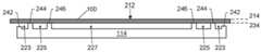
도 1은 임프린트 장치의 개념도를 포함한다.
도 2는 도 1의 임프린트 장치의 기판 보유지지기의 처킹 영역에 중첩하는 기판의 단면도의 예시를 포함한다.
도 3은 도 1의 임프린트 장치의 템플레이트 보유지지기에 의해 보유지지되는 템플레이트의 단면도의 예시를 포함한다.
도 4는 기판의 일부와 템플레이트의 몰드의 측면도를 포함한다.
도 5는 도 1의 임프린트 장치를 사용하여 임프린트된 층을 형성하는 공정 흐름을 포함한다.
도 6은 기판의 일부, 기판 보유지지기의 처킹 영역 및 템플레이트의 몰드의 측면도를 포함한다.
도 7은 성형성 재료에 의한 임프린트 동작 동안의 기판의 일부, 처킹 영역 및 몰드의 측면도를 포함한다.
도 8은 기판 및 임프린트된 폴리머층을 포함하는 작업물의 일부의 단면도의 예시를 포함한다.
도 9는 임프린트된 폴리머층의 잔류층을 제거한 후의 도 8의 작업물의 일부의 단면도의 예시를 포함한다.
도 10은 대안적인 실시예에 따른 도 1의 임프린트 장치를 사용하여 임프린트된 층을 형성하기 위한 공정 흐름을 포함한다.
도 11은 기판 및 임프린트된 폴리머층을 포함하는 작업물의 일부의 단면도의 예시를 포함한다.
도 12는 에칭 저항층을 형성한 후의 도 11의 작업물의 일부의 단면도의 예시를 포함한다.
도 13은 임프린트된 폴리머층의 일부를 노출시키기 위해서 에칭 저항층의 일부를 제거한 후의 도 12의 작업물의 일부의 단면도의 예시를 포함한다.
도 14는 임프린트된 폴리머층의 노출된 부분을 제거한 후의 도 13의 작업물의 일부의 단면도의 예시를 포함한다.
통상의 기술자는 도면의 요소가 단순성 및 명확성을 위해 예시된 것이며 반드시 축척대로 그려진 것은 아니라는 것을 인식한다. 예를 들어, 도면의 요소의 일부의 치수는 본 발명의 실시예의 이해를 향상시키는 것을 돕기 위해서 다른 요소에 대해 과장될 수 있다.The embodiments are illustrated by way of example and are not limited within the accompanying drawings.
1 includes a conceptual diagram of an imprint apparatus.
FIG. 2 includes an example of a cross-sectional view of a substrate overlapping a chucking region of a substrate holder of the imprint apparatus of FIG. 1.
FIG. 3 includes an example of a cross-sectional view of a template held by a template holder of the imprint apparatus of FIG. 1.
4 includes a side view of a part of the substrate and a mold of the template.
5 includes a process flow of forming an imprinted layer using the imprint apparatus of FIG. 1.
6 includes a side view of a portion of the substrate, a chucking region of the substrate holder and a mold of the template.
7 includes a side view of a portion of a substrate, a chucking area, and a mold during an imprint operation with a moldable material.
8 includes an illustration of a cross-sectional view of a portion of a workpiece including a substrate and an imprinted polymer layer.
9 includes an illustration of a cross-sectional view of a portion of the work piece of FIG. 8 after removing the residual layer of the imprinted polymer layer.
10 includes a process flow for forming an imprinted layer using the imprint apparatus of FIG. 1 according to an alternative embodiment.
11 includes an illustration of a cross-sectional view of a portion of a workpiece including a substrate and an imprinted polymer layer.
12 includes an illustration of a cross-sectional view of a portion of the work piece of FIG. 11 after forming an etch resistance layer.
13 includes an illustration of a cross-sectional view of a portion of the work piece of FIG. 12 after removing a portion of the etch resistance layer to expose a portion of the imprinted polymer layer.
14 includes an illustration of a cross-sectional view of a portion of the workpiece of FIG. 13 after removing the exposed portion of the imprinted polymer layer.
Those of skill in the art appreciate that elements in the drawings have been illustrated for simplicity and clarity and have not necessarily been drawn to scale. For example, dimensions of some of the elements in the drawings may be exaggerated for other elements to help improve understanding of embodiments of the present invention.
도면과 조합되는 이하의 설명은 본원에 개시된 교시의 이해를 돕기 위해 제공된다. 이하의 설명은 상기 교시의 특정 구현 및 실시예에 집중할 것이다. 이런 집중은 상기 교시의 설명을 돕기 위해 제공되며 상기 교시의 범위 또는 적용성에 대한 제한으로서 해석되어서는 안된다. 그러나, 다른 실시예는 본 출원에 개시된 바와 같은 교시에 기초할 수 있다.The following description in combination with the drawings is provided to aid in understanding the teachings disclosed herein. The following description will focus on specific implementations and embodiments of the above teachings. This focus is provided to aid in the explanation of the teaching and should not be construed as a limitation on the scope or applicability of the teaching. However, other embodiments may be based on the teachings as disclosed herein.
본원에서 사용되는 바와 같이, 용어 "포함한다", "포함하는", "구비한다", "구비하는", "갖는다", "갖는" 또는 그 임의의 다른 변형은 배타적이지 않은 포함을 포함하도록 의도된다. 예를 들어, 특징의 나열을 포함하는 방법, 물품, 또는 장치는 반드시 그 특징으로만 제한되는 것은 아니고 명시적으로 나열되지 않거나 이러한 방법, 물품 또는 장치에 고유한 다른 특징도 포함할 수 있다. 또한, 명시적으로 반대로 설명되지 않는 한, "또는"은 포함적인 또는을 지칭하며 배타적인 또는을 지칭하지 않는다. 예를 들어, 조건 A 또는 B는 이하 중 어느 하나에 의해 만족된다: A는 사실이고(또는 존재하고) B는 거짓이고(또는 존재하지 않고), A는 거짓이고(또는 존재하지 않고) B는 사실이고(또는 존재하고), 그리고 A 및 B 모두가 사실이다(또는 존재한다).As used herein, the terms “comprises”, “comprising”, “having”, “having”, “having”, “having” or any other variation thereof are intended to include non-exclusive inclusion do. For example, a method, article, or device that includes an enumeration of features is not necessarily limited to that feature and may include other features that are not explicitly listed or that are unique to such a method, article, or device. Further, unless explicitly stated to the contrary, “or” refers to an inclusive or and not an exclusive or. For example, condition A or B is satisfied by either of the following: A is true (or exists), B is false (or does not exist), A is false (or does not exist), and B is Is true (or exists), and both A and B are true (or exists).
또한, 단수형의 사용은 본원에 설명된 요소들 및 구성요소들을 설명하기 위해 사용된다. 이는 단지 편의를 위한 것이며 본 발명의 범위의 일반적인 감을 주기 위한 것이다. 본 설명은 달리 의미하는 것이 명확하지 않은 한 복수도 포함하는 하나, 하나 이상, 또는 단수형을 포함하도록 읽혀져야 하거나 그 반대로도 된다. 예를 들어, 본원에서 단일 품목이 설명될 때, 하나 초과의 품목이 단일 품목 대신에 사용될 수 있다. 마찬가지로, 본원에서 하나 초과의 품목이 설명될 때, 단일 품목이 하나 초과의 품목으로 대체될 수 있다.Also, the use of the singular is used to describe the elements and components described herein. This is for convenience only and is intended to give a general sense of the scope of the present invention. This description should be read to include one, more than one, or the singular, including the plural, or vice versa, unless otherwise indicated. For example, when a single item is described herein, more than one item may be used in place of a single item. Likewise, when more than one item is described herein, a single item may be replaced by more than one item.
달리 규정되지 않는 한, 본원에서 사용되는 모든 기술적 및 과학적 용어는 통상의 기술자에 의해 일반적으로 이해되는 것과 동일한 의미를 갖는다. 재료, 방법 및 예는 단지 예시적인 것이며 제한적인 것으로 의도되지 않는다. 본원에 설명되지 않는 범위에 대해서는, 특정 재료 및 처리 작용에 관한 많은 세부사항은 종래와 같고 임프린트 및 리소그래피 기술분야 내의 텍스트북 및 다른 소스에서 찾을 수 있다.Unless otherwise specified, all technical and scientific terms used herein have the same meaning as commonly understood by one of ordinary skill in the art. The materials, methods, and examples are illustrative only and are not intended to be limiting. To the extent not described herein, many details regarding specific materials and processing operations are conventional and can be found in textbooks and other sources within the imprint and lithography arts.
임프린트 장치 및 방법은 적어도 부분적으로 임프린트 시스템 내의 왜곡을 보상하기 위해 사용될 수 있다. 왜곡은 기판, 임프린트 리소그래픽 템플레이트, 임프린트 장치, 또는 이들의 임의의 조합으로부터 올 수 있다. 왜곡은 이미지 배치 에러로 인한 몰드의 패턴 왜곡 또는 기판 상의 왜곡, 또는 기판 보유지지기 또는 템플레이트 보유지지기의 처킹 영역의 기판 지지면, 기판의 주면 또는 처킹면, 템플레이트의 주면 또는 처킹면, 또는 이들의 임의의 조합의 평면성의 편차를 포함할 수 있다. 실시예에서, 기판은 웨이퍼 형태일 수 있다.The imprint apparatus and method can be used at least in part to compensate for distortion in the imprint system. Distortion can come from the substrate, imprint lithographic template, imprint apparatus, or any combination thereof. Distortion is the pattern distortion or distortion on the substrate due to image placement error, or the substrate support surface of the substrate holder or the chucking area of the template holder, the main surface or the chucking surface of the template, the main surface or the chucking surface of the template, or these Any combination of may include deviations in planarity. In embodiments, the substrate may be in the form of a wafer.
예를 들어, 기판이 처킹 영역 위에 배치될 때, 기판의 노출면은 형성된 임프린트된 층과 기판 내의 미리 형성된 패턴화된 층 사이의 상당한 중첩 차를 초래할 수 있는 척의 평면성으로부터의 편차로 인한 평면내 왜곡을 나타낼 수 있다. 척의 평면성으로부터의 편차로 인한 기판의 평면내 왜곡은 진공 처킹 동안 척에 정합되는 기판으로 인한 것이다. 노출된 면의 편평도가 측정될 수 있고, 성형성 재료에 대한 분배 패턴이 반대 방향의 몰드의 평면성으로부터의 의도적인 또는 프로그래밍된 편차를 유발하도록 조정되어 기판 내의 패턴화된 층에 대한 향상된 정합을 허용할 수 있다. 기판 척에 의해 유발되는 평면성의 편차는 기판의 평면내 왜곡을 유발한다. 이 평면내 왜곡은 평면성으로부터의 의도적인 또는 프로그래밍된 편차에 의해 몰드에 형성된다. 이 프로그래밍된 편차는, 도 7에 동일하게 그리고 반대로 도시되어 있지만, 특히 몰드 및 기판의 두께 및 재료 특성에 따라 변할 수 있다. 이 평면내 왜곡 매칭은 향상된 중첩으로 이어지고 결국 디바이스 수율에 영향을 준다. 이상적인 점 격자에 비교되는 이미지 배치 에러 또는 평면내 왜곡은 몰드와 기판 모두에 동일한 정도로 존재할 것이다.For example, when a substrate is placed over the chucking area, the exposed surface of the substrate is in-plane distortion due to deviations from the planarity of the chuck, which can lead to significant overlap differences between the imprinted layer formed and the preformed patterned layer within the substrate. Can represent. The in-plane distortion of the substrate due to deviation from the planarity of the chuck is due to the substrate mating to the chuck during vacuum chucking. The flatness of the exposed side can be measured, and the dispensing pattern for the moldable material is adjusted to cause an intentional or programmed deviation from the planarity of the mold in the opposite direction, allowing for improved registration to the patterned layer within the substrate. can do. The deviation of planarity caused by the substrate chuck causes in-plane distortion of the substrate. This in-plane distortion is formed in the mold by intentional or programmed deviations from planarity. This programmed deviation is shown in FIG. 7 the same and vice versa, but can vary depending on the material properties and thickness of the mold and substrate in particular. This in-plane distortion matching leads to improved superposition, which in turn affects device yield. Image placement errors or in-plane distortion compared to an ideal dot grid will be present to the same extent in both the mold and the substrate.
결과적인 임프린트된 폴리머층의 잔류층은 허용가능한 양의 비균일성을 갖는다(예를 들어, 잔류층은 과도하게 많은 돌출부의 침식 없이 제거될 수 있다). 비균일성의 양이 과도하게 높은 경우, 에칭 저항층을 갖는 역 이미지가 사용될 수 있다. 역 이미지 공정에 대해서는, 폴리머층의 돌출부가 제거될 수 있고, 잔류층의 일부가 에칭 저항층에 의해 덮인 상태로 남겨진다. 따라서, 상기 방법은 상이한 양의 비균일성을 갖는 잔류층을 고려하는데 충분이 유연하다. 상기 장치 및 방법은 임의의 패턴화된 층을 형성하는데 사용될 수 있으며 특히 30 nm 이하의 매우 작은 치수를 갖는 패턴화된 층에 잘 맞는다.The residual layer of the resulting imprinted polymer layer has an acceptable amount of non-uniformity (eg, the residual layer can be removed without erosion of excessively large protrusions). When the amount of non-uniformity is excessively high, an inverse image with an etch resistant layer can be used. For the reverse imaging process, the protrusions of the polymer layer can be removed, and a portion of the residual layer is left covered by the etch resistant layer. Thus, the method is flexible enough to take into account residual layers with different amounts of non-uniformities. The above apparatus and methods can be used to form any patterned layer and are particularly well suited to patterned layers with very small dimensions of 30 nm or less.
다른 예는 평면성의 편차가 크기 않지만 몰드가 패턴 왜곡을 갖거나 기판이 미리 패턴화된 필드에서 이미지 배치 에러로 인한 왜곡을 갖는 경우이다. 왜곡은 크기 왜곡과 사행 왜곡 또는 사다리꼴 왜곡 같은 직교성 왜곡을 포함할 수 있다. 이러한 왜곡은 측정될 수 있고 분석에 이용될 수 있다. 성형성 층을 갖는 몰드의 평면성으로부터의 전술한 프로그래밍된 편차를 생성함으로써, 몰드 또는 기판의 왜곡으로 인해 발생하는 중첩 에러를 감소시키는 평면내 왜곡이 생성될 수 있다. 왜곡은 정량화될 수 있고, 분배 패턴이 그에 따라 조정된다. 상기 장치 및 방법은 도면과 관련하여 본 명세서를 읽은 후에 더 잘 이해된다.Another example is the case where the deviation of planarity is not large, but the mold has pattern distortion or the substrate has distortion due to image placement error in a pre-patterned field. Distortion may include size distortion and orthogonal distortion such as meandering distortion or trapezoidal distortion. This distortion can be measured and used for analysis. By creating the above-described programmed deviation from the planarity of the mold with the formable layer, an in-plane distortion can be created that reduces the overlap error that occurs due to distortion of the mold or substrate. Distortion can be quantified and the distribution pattern is adjusted accordingly. The apparatus and method will be better understood after reading this specification in connection with the drawings.
도 1은 기판(100) 상에 릴리프(relief) 패턴을 형성하기 위해 사용될 수 있는 나노임프린트 리소그래피 시스템(110)을 예시한다. 기판(100)은 기판 보유지지기(114)에 결합될 수 있다. 예시된 바와 같이, 기판 보유지지기(114)는 진공 척이다. 기판 보유지지기(114) 내의 구역은 기체 제어기(136)와 유체 소통할 수 있다. 대안적으로, 기판 보유지지기(114)는 진공, 핀-타입, 그루브-타입, 정전기형, 전자기형 등을 포함하는 임의의 척일 수 있다. 예시적인 척이 그 전체가 참조로 본원에 통합되는 미국 특허 제6,873,087호에 설명되어 있다.1 illustrates a
기판(100) 및 기판 보유지지기(114)는 스테이지(116)에 의해 더 지지될 수 있다. 스테이지(116)는 x, y, 및 z 축을 따른 병진 운동, 회전 운동, 또는 병진 및 회전 운동 모두를 제공할 수 있다. 스테이지(116), 기판(100) 및 기판 보유지지기(114)는 베이스(도시되지 않음) 상에 위치될 수도 있다.The
템플레이트(118)는 기판(100)으로부터 이격되어 있다. 템플레이트(118)는 대향 측부를 갖는 몸체를 포함할 수 있고, 대향 측부 중 하나는 크기가 전체 필드에 대응하는 기판(100)을 향해 연장되는 패턴면(122)을 갖는 몰드(120)를 갖는다. 실시예에서, 몰드(120)는 메사 형태일 수 있다. 다른 실시예에서, 템플레이트(118)는 메사를 포함하지 않는다.The
실시예에서, 템플레이트(118), 몰드(120) 또는 양자 모두는 용융 실리카, 석영, 실리콘, 유기 중합체, 실록산 폴리머, 보로실리케이트 유리, 프루오로카본 폴리머, 금속, 경화 사파이어, 원하는 형상으로 몰딩, 기계가공, 또는 에칭될 수 있는 다른 적합한 재료, 또는 이들의 임의의 조합을 포함하는 재료로부터 형성된다. 예시된 바와 같이, 패턴면(122)은 복수의 이격된 리세스(124), 돌출부(126), 또는 리세스 및 돌출부의 임의의 조합에 의해 형성되는 특징을 포함하지만, 실시예들이 이러한 구성으로 제한되는 것은 아니다. 대안적인 실시예에서, 패턴면은 평면을 갖는다. 패턴면(122)은 기판(100) 상에 형성되는 대응하는 패턴의 기초를 형성하는 패턴을 형성한다.In an embodiment, the
예시된 실시예에서, 템플레이트(118)는 템플레이트 척(128)에 결합된다. 템플레이트 척(128)은 진공, 핀-타입, 그루브-타입, 정전기형, 전자기형, 다른 적합한 척 타입, 또는 이들의 임의의 조합으로서 구성될 수 있다. 예시적인 척이 미국특허 제6,873,087호에 더 설명되어 있다. 예시된 바와 같은 실시예에서, 척(128)은 임프린트 헤드(130)에 결합되므로, 템플레이트 척(128), 임프린트 헤드(130), 또는 양자 모두는 서로에 대한 템플레이트(118) 및 기판(100)의 이동을 용이하게 하도록 구성된다. 임프린트 헤드(130)는 프레임(150)에 결합된다.In the illustrated embodiment,
시스템(110)은 유체 분배 시스템(132)을 더 포함할 수 있다. 유체 분배 시스템(132)은 기판(100) 상에 성형성 재료(134)를 퇴적시키기 위해 사용된다. 특정 실시예에서, 성형성 재료는 중합성 재료일 수 있다. 예시된 바와 같은 실시예에서, 성형성 재료(134)는 액적 분배, 스핀 코닝, 딥 코팅, 화학 증착(CVD), 물리 증착(PVD), 박막 퇴적, 후박 퇴적, 또는 이들의 임의의 조합 같은 기술을 사용하여 기판(100)에 위치된다. 성형성 재료(134)는, 설계 고려에 따라 원하는 용적이 패턴면(122)과 기판(100) 사이에 형성된 후에, 그 전에, 또는 전후 모두에 기판(100) 상에 배치된다. 분배 패턴에 관한 세부사항을 본 명세서의 이후의 설명에서 더 상세하게 설명한다.
시스템(110)은 경로(142)를 따라 에너지(140) 지향시키도록 결합되는 에너지원(138)을 더 포함한다. 시스템(110)은 또한 패턴화된 층이 기판(100) 상에 형성되고 나면 재료(134)의 이미지 분포, 템플레이트(118)의 분리, 또는 재료(134)의 이미지 분포 및 템플레이트(118)의 분리 양자 모두를 감시할 수 있는 카메라(158)를 포함한다. 임프린트 헤드(130) 및 스테이지(116)는 템플레이트(118) 및 기판(100)을 경로(142)와 중첩되게 위치시키도록 구성된다. 예시된 바와 같은 실시예에서, 시스템(110)은 적어도 부분적으로 스테이지(116), 임프린트 헤드(130), 유체 분배 시스템(132), 에너지원(138), 또는 이들의 임의의 조합과 통신하는 처리기(154)에 의해 제어되며, 메모리(156)에 저장된 컴퓨터 판독가능 프로그램 상에서 동작될 수 있다. 다른 실시예에서, 처리기(154)는 시스템(110) 외부에 위치될 수 있다. 또 다른 실시예에서, 처리기(154)와 관련하여 설명된 기능은 하나 초과의 처리기에 의해 실행될 수 있으며, 하나 이상의 처리기는 시스템(110)의 내부에 있으며 하나 이상의 다른 처리기는 시스템(110) 외부에 있다. 본 명세서를 읽은 후에, 통상의 기술자는 특정 용례를 위해 필요 또는 원하는 바에 적합화된 임프린트 리소그래피 시스템을 구성할 수 있다.
도 2는 처킹 영역과 기판(100) 사이의 위치 관계를 예시하기 위해 처킹 영역과 기판(100)을 포함하는 기판 척(114)의 일부의 예시를 포함한다. 처킹 영역은 외측 구역(223), 중간 구역(225), 및 중앙 구역(227)을 포함하며, 중간 구역(225)은 외측 구역(223)과 중앙 구역(227) 사이에 배치된다. 구역(223, 225, 및 227) 각각은 부분적으로 리세스된 랜드(land)(242) 및 완전한 높이 랜드(244 및 246)에 의해 형성된다. 특정 실시예에서, 랜드(242, 244, 및 246) 각각은 연속적이며, 따라서 랜드(242, 244, 및 246)는 동심이다. 외측 구역(223)은 랜드(242 및 244)에 의해 측방향으로 형성되고, 중간 구역(225)은 랜드(244 및 246)에 의해 측방향으로 형성되며, 중앙 구역(227)은 랜드(246)에 의해 측방향으로 형성된다. 구역(223, 225, 및 227) 중 임의의 하나 이상 내에서, 하나 이상의 핀(도시되지 않음)이 필요하거나 원하는 바에 따라 기판(100)의 지지를 보조하기 위해 존재할 수 있다. 다른 실시예에서, 리세스된 랜드(242)는 완전한 높이 랜드에 의해 대체될 수 있다.2 includes an illustration of a portion of a
기판 척(114)의 처킹 영역의 주면은 완전한 높이 랜드(244 및 246)의 상면에 의해 형성되며 평면(234)을 따라 놓인다. 기판(100)의 주면(212)은 평면(214)을 따라 놓인다. 이론적으로, 처킹 영역 및 기판(100)의 주면은 완벽하게 편평하며 평면성의 편차가 없다. 실제 용례에서, 처킹 영역, 기판(100), 또는 양자 모두의 주면은 평면성의 적어도 일부의 편차를 가질 수 있다. 기판(100)이 처킹 영역 위에 배치될 때, 기판(100)의 노출된 주면은 처킹 영역 또는 기판(100)의 주면을 따른 평면성의 편차와 상이한 평면성의 편차를 가질 수 있다. 실시예에서, 평면성의 편차는 편평도를 측정함으로써 결정될 수 있으며, 측정을 위한 예시적인 도구는 간섭계, 프로필로미터(profilometer) 등을 포함할 수 있다.The major surface of the chucking area of the
도 1 및 도 3을 참고하면, 템플레이트(118)는 템플레이트 척(128)에 결합된다. 템플레이트 척(128)은 대향 측부(311 및 313)를 포함한다. 측부, 또는 에지, 표면(315)이 대향 측부(311 및 313) 사이에 연장된다. 측부(311)는 이격된 지지 영역(321 및 323)을 형성하는 리세스(317) 및 리세스(317)로부터 이격된 리세스(319)를 포함한다. 지지 영역(321)은 지지 영역(323) 및 리세스(317 및 319)를 둘러싼다. 지지 영역(323)은 리세스(319)를 둘러싼다. 추가의 실시예에서, 지지 영역(321 및 323)은 순응성 재료로 형성된다. 특정 실시예에서, 지지 영역(321)은 정사각형 형상을 갖고, 지지 영역(323)은 원 형상을 갖지만, 추가적인 실시예에서, 지지 영역(321 및 323)은 원하는 임의의 기하학적 형상을 구비할 수 있다. 템플레이트 척(128)의 일부(347)는 리세스(319)와 중첩되며 미리결정된 파장 또는 다양한 파장을 갖는 방사선에 대해 투명할 수 있다. 부분(347)은 유리 같은 투명한 재료의 박층을 구비할 수 있다. 그러나, 부분(347)의 재료는 에너지원에 의해 방출되는 방사선의 파장에 의존할 수 있다. 부분(347)은 측부(313) 사이에서 연장되며 리세스(319) 가까이에서 종료된다. 부분(347)은 몰드(120)가 그것과 중첩되도록 적어도 몰드(120)의 면적만큼의 면적을 갖는다.1 and 3, the
템플레이트 척(128)은 통로(327 및 329)를 구비한다. 대안적인 실시예에서, 템플레이트 척(128)은 상이한 수의 통로를 가질 수 있다. 통로(327)는 리세스(317)를 표면(313)과 유체 소통하는 상태가 되게 하지만, 추가적인 실시예에서 통로(327)는 리세스(317)를 템플레이트 척(128)과 유체 소통하는 상태가 되게 한다. 통로(329)는 리세스(319)를 측부(313)와 유체 소통하는 상태가 되게 하지만, 추가적인 실시예에서 통로(329)는 리세스(319)를 템플레이트 척(128)의 임의의 표면과 유체 소통하는 상태가 되게 한다. 통로(327 및 329)는 리세스(317 및 319)를 각각 펌프 시스템(331) 같은 압력 제어 시스템과 유체 소통하는 상태가 되게 하는 것을 용이하게 한다.
펌프 시스템(331)은 리세스(317 및 319)에 가까운 압력을 제어하기 위한 하나 이상의 펌프를 구비할 수 있다. 이를 위해, 템플레이트(118)는 템플레이트 척(128)에 결합되고, 템플레이트(118)는 지지 영역(321 및 323)에 놓여 리세스(317 및 319)를 덮는다. 템플레이트(118)의 가요성 영역(338)이 리세스(319)와 중첩되어 챔버(333)를 형성할 수 있으며, 템플레이트(118)의 더 두꺼운 영역(340)이 리세스(317)와 중첩되어 챔버(335)를 형성할 수 있다. 펌프 시스템(331)은 챔버(333 및 335) 내의 압력을 제어하도록 동작한다.The
이론적으로, 몰드(120)의 주면(320)은 완벽하게 편평하며 평면성의 편차를 갖지 않는 것이 바람직하다. 실제 용례에서, 몰드(120)의 주면은 평면성의 적어도 일부의 편차를 가질 수 있다. 실시예에서, 평면성의 편차는 편평도를 측정함으로써 획득될 수 있으며, 측정을 위한 예시적인 도구는 간섭계, 프로필로미터 등을 포함할 수 있다.In theory, it is preferable that the
이하는 평면성의 편차를 고려할 수 있으며 성형성 재료로부터 형성되는 패턴화된 층과 기판(100)의 미리 형성된 패턴화된 층 사이의 더 양호한 중첩을 허용할 수 있는 예시적인 방법의 설명이다. 특정 실시예와 관련하여 많은 세부사항이 설명되지만, 첨부된 청구항의 범위는 설명된 실시예만으로 제한되지 않는다. 예를 들어, 본원에 설명된 바와 같은 개념 내에서 더 많거나, 더 적거나, 또는 다른 작용이 실행될 수 있다. 도면과 연계하여 본 명세서 전체를 읽은 후에, 통상의 기술자는 본 발명의 범위 내에서 다른 변형이 이루어질 수 있다는 것을 인식할 것이다.The following is a description of an exemplary method that may take into account variations in planarity and allow better overlap between a patterned layer formed from a moldable material and a pre-formed patterned layer of the
도 4는 기판(100) 및 템플레이트(118)의 몰드(120)를 예시한다. 간략화를 위해, 몰드(120)는 패턴화되지 않은 면으로서 예시되어 있으므로, 몰드(120)의 주면을 따른 평면성의 편차는 본 특정 실시예에서는 중요하지 않다. 마찬가지로, 기판(100)의 주면은 본 특정 실시예에서 중요하지 않은 평면성의 편차를 갖는 것으로 예시되어 있다.4 illustrates the
상기 방법은 도 1 및 도 5와 관련하여 더 설명된다. 상기 방법은 도 5의 블록 502에서 기판 척(114)의 처킹 영역 상에 기판(100)을 배치하는 단계를 포함할 수 있다. 도 6은 기판(100) 및 대상물(600)로서의 기판 척(114)의 처킹 영역 사이의 조합을 예시한다. 따라서, 대상물의 노출면(612)은 처킹 영역에 배치될 때 기판(100)의 주면(212)에 대응한다. 본 실시예에서, 처킹 영역은 기판(100)의 형상을 왜곡시켜 평면성의 상당한 편차를 가져온다. 위치(622)는 노출면(612)의 평균 높이보다 높은 높이에 놓이며, 위치(642)는 노출면(612)의 평균 높이보다 낮은 높이에 놓인다. 노출면(612)의 평면성의 편차는 몰드(120)가 정렬되는 기판(100) 내에 이미 존재하는 패턴화된 층의 평면내 왜곡을 가져올 수 있다.The method is further described in connection with FIGS. 1 and 5. The method may include placing the
이하에서 설명되는 바와 같이, 성형성 재료에 대한 분배 패턴은 적어도 부분적으로 임프린트 시스템 내의 왜곡을 고려할 것이다. 분배 패턴을 결정하기 전해, 정보가 보정될 필요가 있다. 상기 방법은 블록 522에서 몰드(120)의 패턴을 결정하는 단계를 포함할 수 있다. 패턴은 앞서 설명된 바와 같이 몰드(120)의 돌출부 및 오목부에 대응한다. 이런 결정은 몰드(120)를 설계 및 형성하기 위해 사용되는 그래픽 데이터 시스템(Graphics Data System)(GDS) 파일을 사용하여 이루어질 수 있다. 성형성 재료의 더 높은 면 밀도는 몰드(120)의 오목부가 존재하는 위치에 분배될 것이고, 성형성 재료의 더 낮은 면 밀도는 몰드(120)의 돌출부가 존재하는 위치에 분배될 것이다.As explained below, the dispensing pattern for the formable material will at least partially account for distortion within the imprint system. Before determining the distribution pattern, the information needs to be corrected. The method may include determining a pattern of
상기 방법은 블록(524)에서 임프린트 시스템 내의 왜곡을 정량화하는 단계를 포함할 수 있다. 임프린트 시스템은 기판(100), 템플레이트(118) 및 장치를 포함할 수 있다. 왜곡을 정량화하는 단계는 임프린트 장치 내의 구성요소의 면을 따른 평면성의 편차를 결정하는 단계를 포함할 수 있다. 평면성의 편차는 처킹 영역의 주면, 기판(100)의 주면(212), 몰드(120)의 주면, 또는 이들의 임의의 조합을 따른 편평도로서 측정될 수 있다. 도 6에 예시된 실시예에서, 편평도는 기판(100)이 기판 척(114)의 처킹 영역 위에 있을 때 기판의 주면(212)을 따라 측정된다. 편평도는 전체 또는 거의 전체 기판(100)(예를 들어, 모든 임프린트 필드), 단일 임프린트 필드, 임프린트 필드의 선택된 조합(예를 들어, 특정 임프린트 필드 및 바로 인접하는 임프린트 필드들) 등에 대해 측정될 수 있다. 높이가 낮은 영역에 대해서는, 높은 면 밀도의 성형성 재료가 분배될 것이고, 높이가 높은 영역에 대해서는 낮은 면 밀도의 성형성 재료가 분배될 것이다. 면 밀도의 차의 원인은 본 명세서에서 이후에 설명될 것이다.The method may include quantifying the distortion in the imprint system at
다른 왜곡은 배율 또는 직교성 왜곡일 수 있다. 특정 실시예에서, 기판(100)의 미리 형성된 패턴은 템플레이트(118)의 몰드에 비해 과도하게 작거나 과도하게 클 수 있다. 이러한 배율 왜곡은 기판(100)의 미리 형성된 패턴의 외측 치수를 몰드의 외측 치수와 비교함으로써 정량화될 수 있다. 미리 형성된 패턴이 템플레이트(118)의 몰드에 대해 과도하게 작은 경우, 몰드가 오목한 면을 갖도록 하기 위해 주변부에 비해 임프린트 필드의 중심 부근에 높은 밀도의 성형성 재료가 분배될 수 있고, 이는 성형성 재료 내의 프린트될 필드의 크기를 감소시킨다. 미리 형성된 패턴이 템플레이트(118)의 몰드에 대해 과도하게 큰 경우, 몰드가 볼록한 면을 갖도록 하기 위해 중심에 비해 임프린트 필드의 주변부 부근에 높은 밀도의 성형성 재료가 분배될 수 있고, 이는 성형성 재료 내의 프린트될 필드의 크기를 증가시킨다. 사행 및 사다리꼴 왜곡 같은 직교성 왜곡을 보정하기 위해서 유사한 접근법이 취해질 수 있다.Other distortions may be magnification or orthogonal distortion. In certain embodiments, the preformed pattern of the
상기 방법은 블록 526에서 성형성 재료를 위한 분배 패턴을 결정하는 단계를 더 포함할 수 있다. 몰드(120)의 패턴, 시스템 내의 왜곡, 및 잠재적인 다른 정보에 관한 정보가 메모리(156), 메트롤로지 툴(예를 들어, 간섭계, 프로필로미터 등), 외부 소스(예를 들어, GDS 파일이 예시되지 않은 외부 메모리에 있음), 노출 동안의 상태 정보(노출 동안의 온도, 습도, 에너지원, 면 에너지 밀도 등), 또는 성형성 재료를 위한 패턴화에 영향을 줄 수 있는 다른 적합한 정보로부터 처리기(154)에 의해 수신될 수 있다.The method may further include determining, at
몰드(120)의 패턴에 관한 정보는 왜곡에 비해 분배 패턴에 더 크게 영향을 줄 것이다. 그러나, 왜곡은 특히 잔류층이 형성되는 경우 여전히 분배 패턴에 크게 영향을 준다. 일 영역에 대한 분배 패턴의 면 밀도는 돌출부 또는 오목부에 대응하는 면 밀도(일 영역에 대응하는 몰드(120)의 특징에 따름)와 그 영역의 편평도에 대응하는 면 밀도의 조합일 수 있다.Information about the pattern of the
상기 방법은 블록 528에서 분배 패턴에 따라 성형성 재료를 분배하는 단계를 포함할 수 있다. 분배 패턴이 결정된 후에, 처리기(154)는 주면을 따라 상이한 영역에서 원하는 면 밀도를 달성하도록 기판(100)의 주면 상에 성형성 재료를 분배하기 위해서 유체 분배 시스템(132)에 명령어 또는 신호를 송신할 수 있다.The method may include dispensing the formable material according to the dispensing pattern at
상기 방법은 블록 542에서 템플레이트(118)로 성형성 재료를 임프린트하는 단계를 포함할 수 있다. 도 7은 몰드(120)에 돌출부가 있고 잔류층이 형성되어 있는 영역에서의 대상물(600)(처킹 영역과 기판(100)의 조합)의 일부의 예시를 포함한다. 따라서, 도 7은 몰드(120)의 오목부 또는 몰드(120)의 오목부에 대응하는 성형성 재료(700)의 돌출부를 예시하지 않지만, 이러한 오목부-돌출부 조합이 존재할 수 있다. 기판의 위치(622 및 642)는 템플레이트의 대응하는 위치(722 및 742)를 갖는다. 도 7에서 볼 수 있는 바와 같이, 선(762)이 성형성 재료(700)의 두께를 양분하여, 성형성 재료는 선(762)에 대해 미러 이미지를 갖는다. 이 미러 이미지는 3차원이다. 즉, 도 7은 임프린트의 단면을 도시하지만, 도시된 바와 같은 몰드 및 기판의 형상은 국소적인 편평도에 따라 임프린트 영역을 가로질러 변할 수 있는 것이 이해될 것이다. 그러므로, 성형성 재료(700)에 대한 미러 이미지는 기판(100)의 이미 존재하는 패턴화된 층에 대한 성형성 재료(700)로 성형되는 패턴의 중첩을 향상시키기 위해서 노출면(612)을 따라 왜곡의 형상을 감소 또는 상쇄하는 것을 도울 수 있다. 비균일성의 중요성은 본 명세서에서 이후에 더 명확해질 것이다.The method may include imprinting the formable material into
상기 방법은 도 5의 블록 544에서 폴리머층을 형성하기 위해 성형성 재료를 에너지에 노출시키는 단계를 더 포함할 수 있다. 도 1을 참조하면, 성형성 재료의 조성은 에너지원(138)으로부터의 에너지(140)에 노출될 때 폴리머층을 형성하도록 교차결합 또는 중합하도록 선택된다. 실시예에서, 에너지원(138)은 방사선을 방출하고 성형성 재료는 방사선에 응답하는 활성화제를 포함할 수 있다. 특정 실시예에서, 방사선은 자외선이다. 다른 실시예에서, x선 또는 가시광 같은 상이한 방사선에 응답하는 상이한 조성의 성형성 재료를 사용할 수 있다. 폴리머층의 형상은 몰드(120)와 접촉하고 있을 때 성형성 재료와 실질적으로 동일하다.The method may further include exposing the moldable material to energy to form the polymer layer at
상기 방법은 도 5의 블록 546에서 폴리머층으로부터 템플레이트(118)를 분리하는 단계를 포함할 수 있다. 분리를 위한 많은 상이한 기술이 통상의 기술자에게 알려져 있다. 본 명세서를 읽은 후에, 통상의 기술자는 특정 용례에 대한 필요 또는 요망을 충족하는 특정 분리 기술을 선택할 수 있을 것이다.The method may include separating the
설명된 바와 같은 실시예의 이점은 임프린트된 층과 기판(100) 내의 하부 패턴화된 층 사이의 향상된 중첩이다. 제조 기술은 기판 보유지지기(114), 기판(100) 또는 양자 모두의 처킹 영역에 대해 달성될 수 있는 편평도를 제한할 수 있다. 결과는 기판(100)의 평면내 왜곡을 초래할 수 있는 평면밖 비편평도일 수 있다. 본 발명 전에, 나노임프린트 기술은, 잔류층이 폴리머층 내의 돌출부의 과도하게 많은 두께(높이)를 제거하지 않으면서 더 용이하게 제거될 수 있도록 잔류층이 가능한 얇고 균일하게 유지되도록 실행되었다. 노출면(612)이 평면형이 아닌 경우, 균일하고 얇은 잔류층은 비평면 노출면(612)이 기판(100) 상의 것과 자국이 반대인 템플레이트(118)의 평면내 왜곡을 유발하기 때문에 문제를 악화시킬 수 있다. 2개의 평면내 왜곡 사이의 차이인 결과적인 중첩은 따라서 템플레이트(118) 및 기판, 또는 양자 모두의 처킹 영역의 편평도의 함수이다.An advantage of the embodiment as described is an improved overlap between the imprinted layer and the underlying patterned layer in the
종래의 교시와 대조적으로, 상기 방법은 노출면(612)을 따른 평면내 왜곡의 영향을 상쇄하는 것을 돕는 상보적인 평면밖 왜곡을 유발한다. 그러므로, 노출면(612)의 평면성의 편차로 인한 중첩 에러가 감소 또는 실질적으로 제거될 수 있다. 따라서, 패턴화된 폴리머층은 하부 패턴화된 층 중 하나 이상에 더 정확하게 정렬된다.In contrast to conventional teaching, the method induces complementary out-of-plane distortion that helps to counteract the effects of in-plane distortion along exposed
기판(100)이 반도체 웨이퍼이고 폴리머층이 패턴을 갖는 실시예에서, 잔류층 두께는 15 nm의 공칭 두께를 가질 수 있고, 돌출부는 45 nm 내지 60 nm의 범위일 수 있다. 잔류층 두께는 그 평균 두께의 10% 내지 90% 또는 5 nm 내지 95 nm일 수 있다. 종래, 잔류층은 그 평균 두께의 10% 내지 30% 또는 5 nm 내지 30 nm의 두께를 갖는다. 따라서, 본원에서 설명되는 바와 같은 공정은 잔류층 두께의 비균일성의 상당한 증가를 가져올 수 있고, 이는 통상적인 개념과 대조적이다. 그러나, 많은 경우에, 잔류층의 증가된 비균일성은 문제가 되지 않는다.In an embodiment in which the
실시예에서, 도 8 및 도 9는 성형성 재료(700)가 노출되고 몰드(120)가 제공된 후의 기판(100) 및 폴리머층(800)의 일부의 단면도의 예시를 포함한다. 도 8에서, 폴리머층(800)은 돌출부(822 및 824) 및 돌출부(822 및 824)를 둘러싸는 영역의 잔류층(842)을 포함한다. 임프린트된 폴리머층(800)이 마스크로서 사용될 수 있기 전에, 잔류층(842)은 제거된다. 도 8에 예시된 바와 같이, 잔류층(842)은 일부 왜곡을 갖는 것으로 예시되어 있지만, 왜곡의 정도는 그리 크지 않다. 따라서, 잔류층(842)은 과도하게 많은 돌출부(822 및 824)의 제거 없이 제거될 수 있다. 폴리머층은 유기 화합물일 수 있고 예를 들어 O2, O3, N2O 등의 산소 포함 기체로 제거될 수 있다.In an embodiment, FIGS. 8 and 9 include examples of cross-sectional views of a portion of the
실시예에서, 잔류층(842)은 돌출부(822 및 824)의 측방향 치수를 유지하는 것을 돕기 위해 이방성 에칭을 사용하여 제거될 수 있다. 특정 실시예에서, 에칭은 반응성 이온 에칭을 사용하여 실행될 수 있다. 에칭은 종점 검출(기판(100)이 노출된 것을 나타내는 신호에 기초함)을 이용하는 시간설정(timed) 에칭 또는 종점 검출을 이용하는 시간설정 에칭으로서 실행될 수 있다. 도 9는 잔류층(842)이 제거된 후의 돌출부(922 및 924)의 예시를 포함한다. 돌출부(922 및 924)는 돌출부(922 및 924)가 둥근 상위 코너를 갖는 것을 제외하고 돌출부(822 및 824)와 실질적으로 동일하다.In an embodiment, the
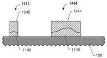
잔류층의 두께가 과도하게 많이 변하는 실시예에서, 공정은 동일한 마스킹 패턴을 달성하도록 변형될 수 있다. 본 실시예에서, 성형성 재료(700)는 도 8 및 도 9에 예시된 바와 같은 실시예와 관련하여 앞서 설명된 바와 같은 패턴을 형성하기 위해 사용되는 역 이미지 패턴을 갖는 몰드로 임프린트된다. 도 10은 도 11 내지 도 14에 예시된 바와 같이 이러한 마스킹 패턴을 달성하기 위한 공정 흐름을 포함한다.In embodiments where the thickness of the residual layer varies excessively, the process can be modified to achieve the same masking pattern. In this embodiment, the
상기 방법은 도 10의 블록 1002에서 역 이미지의 원하는 마스킹 패턴을 갖는 임프린트된 폴리머층을 형성하는 단계를 포함한다. 도 11은 기판(100) 및 기판(100) 위의 임프린트된 폴리머층(1100)을 포함하는 작업물의 일부의 단면도를 포함한다. 임프린트된 폴리머층(1100)은 도 5의 공정과 관련하여 앞서 설명된 바와 같은 기술을 사용하여 형성된다. 이 특정 실시예에서, 왜곡의 정도는 도 8의 폴리머층(800)에 비해 상당히 크다. 임프린트된 폴리머층(1100)은 잔류층(842)의 일부가 도 8에 보여지는 돌출부(1122, 1124, 및 1126) 및 돌출부(822 및 824)가 도 8에 보여지는 도 11의 오목부(1142 및 1144)를 갖는다. 잔류층의 부분(1143 및 1145)은 각각 오목부(1142 및 1144)의 저부를 따라 놓인다. 잔류층, 특히 부분(1145)은 두께가 상당히 더 비균일하다. 이러한 비균일한 두께가 도 8의 잔류층(842)에 형성된 경우, 잔류층(842)이 제거될 때 과도하게 많은 돌출부(822 및 824)가 제거될 수 있다. 결과적인 마스킹 층은 후속 에칭 동작을 견디는데 불충분한 높이(두께)를 가질 수 있는 돌출부(822 및 824)를 가질 것이다. 역 이미지 공정은 잔류층이 더 비균일한 것을 허용하고 여전히 충분히 강겅한 마스킹 패턴을 제공한다.The method includes forming an imprinted polymer layer having a desired masking pattern of an inverse image at
상기 방법은 도 10의 블록 1022에서 임프린트된 폴리머층(1100)의 오목부 내에 에칭 저항층(1200)을 형성하는 단계를 더 포함할 수 있다. 도 12에서, 에칭 저항층(1200)은 임프린트된 폴리머층(1100) 위에 형성되고 오목부(1142 및 1144)(도 11) 내에 그리고 임프린트된 폴리머층(1100)의 부분(1143 및 1145) 위에 형성되는 부분(1242 및 1244)을 포함한다. 예시된 실시예에서, 임프린트된 폴리머층(1100) 모두는 돌출부(1122 및 1124)를 포함한다. 다른 실시예에서, 에칭 저항층(1200)은 돌출부(1122, 1124 및 1126) 위에 거의 형성되지 않거나 전혀 형성되지 않는다.The method may further include forming an
에칭 저항층(1200)의 조성은 임프린트된 폴리머층(1100)이 에칭 저항층(1200)에 비해 선택적으로 에칭될 수 있도록 선택된다. 특정 실시예에서, 임프린트된 폴리머층(1100)은 유기 폴리머를 포함할 수 있으며, 에칭 저항층(1200)은 실리콘 함유 화합물을 포함할 수 있다. 특정 실시예에서, 임프린트된 폴리머층(1100)은 카본 백본을 갖는 유기 폴리머일 수 있다. 다른 특정 실시예에서, 에칭 저항층(1200)은 폴리실록산 같은 실리콘 백본을 갖는 폴리머일 수 잇다.The composition of the
상기 방법은 도 10의 블록 1042에서 돌출부(1122, 1124, 및 1126)를 덮는 에칭 저항층(1200)의 일부를 제거하는 단계를 포함할 수 있다. 도 13에서, 에칭 저항층(1200)의 일부는 에칭 저항층(1200)의 재료를 에칭할 수 있는 에칭제로 에칭 저항층(1200)을 에칭함으로써 제거될 수 있다. 에칭 저항층(1200)이 실리콘을 포함하는 경우, 플루오린 기반 에칭제가 사용될 수 있다. 에칭은 등방성 또는 이방성 에칭일 수 있다. 건식 에칭에 대해, CF4, CHF3, SF6 등과 같은 기체가 사용될 수 있다. 습식 에칭에 대해, 완충 HF 용액(NH4F를 포함)이 사용될 수 있다. 에칭은 종점 검출(임프린트된 폴리머층(1100)이 노출된 것을 나타내는 신호에 기초함)을 이용한 시간설정 에칭 또는 종점 검출을 이용한 시간설정 에칭으로서 실행될 수 있다.The method may include removing a portion of the
상기 방법은 도 10의 블록 1062에서 임프린트된 폴리머층(1100)의 돌출부(1122, 1124 및 1126)를 제거하는 단계를 더 포함할 수 있다. 임프린트된 폴리머층(1100)의 돌출부(1122, 1124, 및 1126)는 잔류층(842)을 제거하는 단계와 관련하여 앞서 설명된 바와 같은 기술 및 기체 중 임의의 것을 사용하여 제거될 수 있다. 마스킹 부재(1442)는 임프린트된 폴리머층(1100)의 부분(1143) 및 에칭 저항층(1200)의 부분(1242)을 포함하며, 마스킹 부재(1444)는 임프린트된 폴리머층(1100)의 부분(1145) 및 에칭 저항층(1200)의 부분(1244)을 포함한다.The method may further include removing the
도 9 및 도 14를 비교하면, 마스킹 부재의 조성은 상이할 수 있지만, 마스킹 패턴은 동일하다. 따라서, 결과적인 잔류층이 충분히 균일한 두께를 갖지 않는 경우에도, 양호한 중첩 특징을 갖는 마스킹 패턴이 달성될 수 있다.9 and 14, the composition of the masking member may be different, but the masking pattern is the same. Thus, even when the resulting residual layer does not have a sufficiently uniform thickness, a masking pattern with good overlapping characteristics can be achieved.
여기 설명된 바와 같은 실시예는 기판 보유지지기(114), 기판(100), 템플레이트(118)의 몰드(120), 또는 이들의 임의의 조합의 처킹 영역이 시스템 내에서 상당한 왜곡을 갖는 경우에도 더 양호한 중첩을 허용한다. 평면성의 편차에 대해, 처킹 영역, 처킹 영역 상에 있을 때의 기판(100)의 노출면, 또는 몰드(120) 중 임의의 것의 편평도가 측정될 수 있다. 다른 왜곡에 대해서, 왜곡이 마찬가지로 정량화될 수 있다. 성형성 재료를 위한 분배 패턴은 왜곡을 보정하기 위해 조정될 수 있으며, 분배 패턴이 왜곡에 대해 조정되지 않는다면 다른 결과가 초래될 것이다. 형성되는 최소 치수가 감소함에 따라, 필드와 게이트 레벨 사이, 게이트와 접촉 레벨 사이 등과 같은 중요한 층 사이의 적합한 정렬을 달성하기 위해 바람직한 이러한 조정이 필요해질 수 있다. 다른 실시예에서, 분배 패턴의 조정은 패턴화 순서의 모두가 아닌 일부에 대해서만 사용될 수 있다. 예를 들어, n 웰 영역 또는 p 웰 영역 같은 웰 영역에 대한 정렬 공차 및 결합 패드는 충분히 크며 필드, 게이트 및 접촉 레벨에 비해 큰 정밀도를 필요로 하지 않는다.Embodiments as described herein are also applicable when the
많은 상이한 양태 및 실시예가 가능하다. 이들 양태 및 실시예의 일부가 이하에서 설명된다. 이 명세서를 읽은 후에, 통상의 기술자는 이들 양태 및 실시예가 단지 예시이며 본 발명의 범위를 제한하지 않는다는 것을 인식할 것이다.Many different aspects and embodiments are possible. Some of these aspects and examples are described below. After reading this specification, one of ordinary skill in the art will recognize that these aspects and examples are merely exemplary and do not limit the scope of the invention.
일반적인 설명 또는 예로 위에서 설명된 활동의 일부가 요구되고, 특정 활동의 일부는 요구되지 않을 수 있으며, 하나 이상의 추가적인 활동이 설명된 것 이외에 실행될 수 있다는 것을 유의해야 한다. 또한, 활동이 나열된 순서는 반드시 그들이 실행되는 순서는 아니다.It should be noted that some of the activities described above are required for general descriptions or examples, some of the specific activities may not be required, and one or more additional activities may be performed other than those described. Also, the order in which the activities are listed is not necessarily the order in which they are executed.
이점, 다른 장점 및 문제에 대한 해결책이 특정 실시예와 관련하여 위에서 설명되었다. 그러나, 임의의 이점, 장점, 또는 해결책이 발생되게 하거나 더 두드러지게 할 수 있는 이점, 장점, 문제에 대한 해결책 및 임의의 특징(들)이 청구항 중 임의의 것 또는 모두의 중요한, 요구되는, 또는 본질적인 특징으로서 해석되는 것은 아니다.Advantages, other advantages and solutions to problems have been described above in connection with specific embodiments. However, the advantage, advantage, solution to a problem, and any feature(s) that may cause or make any advantage, advantage, or solution occur or become more pronounced are important, required, or of any or all of the claims. It is not to be interpreted as an essential feature.
본원에서 설명되는 실시예의 명세 및 예시는 다양한 실시예의 구조의 일반적인 이해를 제공하도록 의도된다. 상기 명세 및 예시는 본원에서 설명되는 구조 또는 방법을 사용하는 장치 및 시스템의 요소 및 특징 모두의 철저한 그리고 포괄적인 설명으로서의 역할을 하도록 의도되지 않는다. 별개의 실시예가 조합되어 또는 단일 실시예로 제공될 수도 있으며, 반대로 간결성을 위해 단일 실시예의 상황에서 설명되는 다양한 특징이 개별적으로 또는 임의의 하위조합으로 제공될 수도 있다. 또한, 범위로 기술된 값에 대한 참조는 그 범위 내의 각각의 및 모든 값을 포함한다. 많은 다른 실시예는 본 명세서를 읽은 후에만 통상의 기술자에게 명확해질 수 있다. 다른 실시예는, 구조적 치환, 논리적 치환, 또는 다른 변경이 본 개시내용의 범위 내에서 이루어질 수 있도록, 본 개시내용으로부터 사용되고 유도될 수 있다. 따라서, 본 개시내용은 제한이 아닌 예시로서 간주되어야 한다.The specification and illustrations of the embodiments described herein are intended to provide a general understanding of the structure of the various embodiments. The above specification and examples are not intended to serve as a thorough and comprehensive description of all elements and features of devices and systems using the structures or methods described herein. Separate embodiments may be provided in combination or as a single embodiment, and conversely, for the sake of brevity, various features described in the context of a single embodiment may be provided individually or in any subcombination. Also, references to values stated in ranges include each and every value within that range. Many other embodiments may become apparent to a person skilled in the art only after reading this specification. Other embodiments may be used and derived from this disclosure so that structural substitutions, logical substitutions, or other changes may be made within the scope of the disclosure. Accordingly, the present disclosure is to be regarded as an illustration and not a limitation.
Claims (10)
Translated fromKorean기판을 위한 기판 지지면을 갖는 처킹 영역(chucking region)을 구비하는 기판 보유지지기;
하나 이상의 돌출부를 구비하는 임프린트면을 갖는 임프린트 리소그래픽 템플레이트를 위한 템플레이트 보유지지기; 및
상기 기판의 왜곡, 상기 임프린트 리소그래픽 템플레이트의 주면을 따른 평면성의 편차, 상기 임프린트 장치 내의 구성요소의 표면을 따른 평면성의 편차, 또는 이들의 임의의 조합에 적어도 부분적으로 기초하여, 특정 영역에 소정량의 성형성 재료를 분배하도록 구성된 처리기를 포함하고,
상기 처리기는, 또한, 상기 왜곡에 적어도 부분적으로 기초하여 상기 성형성 재료에 대한 분배 패턴을 결정하도록 구성되고,
상기 분배 패턴의 결정은,
상기 성형성 재료가,
상기 임프린트 리소그래픽 템플레이트가 제1 영역 내의 성형성 재료에 접촉할 때 상기 왜곡이 상기 하나 이상의 돌출부 및 상기 기판의 주면이 멀리 떨어지게 되는 것을 나타내는, 상기 제1 영역 내의 제1 면 밀도; 및
상기 임프린트 리소그래픽 템플레이트가 제2 영역 내의 성형성 재료에 접촉할 때 상기 왜곡이 상기 하나 이상의 돌출부 및 상기 기판의 주면이 서로 가까워지는 것을 나타내는, 상기 제2 영역 내의 제2 면 밀도
로 분배되도록 실행되며,
상기 제1 면 밀도는 상기 제2 면 밀도보다 큰, 임프린트 장치.It is an imprint device,
A substrate holder having a chucking region having a substrate support surface for the substrate;
A template holder for an imprint lithographic template having an imprint surface having one or more protrusions; And
A predetermined amount in a specific area based at least in part on the distortion of the substrate, the deviation of planarity along the main surface of the imprint lithographic template, the deviation of planarity along the surface of the component in the imprint apparatus, or any combination thereof. A processor configured to dispense the moldable material of,
The processor is further configured to determine a distribution pattern for the formable material based at least in part on the distortion,
The determination of the distribution pattern,
The moldable material,
A first areal density in the first area, wherein the distortion indicates that the one or more protrusions and the major surface of the substrate become distant when the imprint lithographic template contacts the formable material in the first area; And
A second areal density in the second region, wherein the distortion indicates that the one or more protrusions and the major surface of the substrate come close to each other when the imprint lithographic template contacts the formable material in the second region.
Is executed to be distributed as
The imprint apparatus, wherein the first areal density is greater than the second areal density.
주면을 형성하는 하나 이상의 돌출부를 구비하는 임프린트면을 갖는 임프린트 리소그래픽 템플레이트를 제공하는 단계;
기판 지지면을 갖는 처킹 영역을 구비하는 기판 보유지지기를 제공하는 단계;
상기 처킹 영역 위에, 임프린트 영역 내의 주면을 갖는 상기 기판을 배치하는 단계;
상기 기판의 왜곡, 상기 임프린트 리소그래픽 템플레이트의 주면을 따른 평면성의 편차, 상기 임프린트 장치 내의 구성요소의 표면을 따른 평면성의 편차, 또는 이들의 임의의 조합을 정량화하는 단계; 및
상기 기판의 왜곡, 상기 임프린트 리소그래픽 템플레이트의 주면을 따른 평면성의 편차, 상기 임프린트 장치 내의 구성요소의 표면을 따른 평면성의 편차, 또는 이들의 임의의 조합에 적어도 부분적으로 기초하여, 상기 기판의 주면 위에 성형성 재료를 분배하는 단계를 포함하고,
상기 성형성 재료를 분배하는 단계는,
상기 성형성 재료가,
상기 임프린트 리소그래픽 템플레이트가 제1 영역 내의 성형성 재료에 접촉할 때 상기 편차가 상기 하나 이상의 돌출부 및 상기 주면이 멀리 떨어지게 되는 것을 나타내는, 상기 제1 영역 내의 제1 면 밀도; 및
상기 임프린트 리소그래픽 템플레이트가 제2 영역 내의 성형성 재료에 접촉할 때 상기 편차가 상기 하나 이상의 돌출부 및 상기 주면이 서로 가까워지는 것을 나타내는, 상기 제2 영역 내의 제2 면 밀도
로 분배되도록, 실행되며,
상기 제1 면 밀도는 상기 제2 면 밀도보다 큰, 임프린트 장치를 사용하는 임프린트 방법.It is an imprint method using an imprint device,
Providing an imprint lithographic template having an imprint surface having one or more protrusions defining a major surface;
Providing a substrate holder having a chucking region having a substrate support surface;
Disposing the substrate having a main surface in an imprint area over the chucking area;
Quantifying a distortion of the substrate, a deviation of planarity along a major surface of the imprint lithographic template, a deviation of planarity along a surface of a component in the imprint apparatus, or any combination thereof; And
Based at least in part on the distortion of the substrate, the deviation of planarity along the major surface of the imprint lithographic template, the deviation of planarity along the surface of the component in the imprint apparatus, or any combination thereof, on the major surface of the substrate. Dispensing a moldable material,
Dispensing the moldable material comprises:
The moldable material,
A first areal density in the first area, wherein the deviation indicates that the one or more protrusions and the major surface become distant when the imprint lithographic template contacts the formable material in the first area; And
A second areal density in the second region, wherein the deviation indicates that the one or more protrusions and the major surface become close to each other when the imprint lithographic template contacts the formable material in the second region.
To be distributed, executed,
An imprint method using an imprint apparatus, wherein the first areal density is greater than the second areal density.
상기 폴리머층은 상기 제1 영역 내의 제1 두께 및 상기 제2 영역 내의 제2 두께를 갖고, 상기 제1 두께는 상기 제2 두께보다 두꺼운, 임프린트 장치를 사용하는 임프린트 방법.The method of claim 3, further comprising exposing the moldable material to ultraviolet light to polymerize the moldable material and form a polymer layer,
The polymer layer has a first thickness in the first region and a second thickness in the second region, and the first thickness is thicker than the second thickness.
Applications Claiming Priority (2)
| Application Number | Priority Date | Filing Date | Title |
|---|---|---|---|
| US15/162,130US9993962B2 (en) | 2016-05-23 | 2016-05-23 | Method of imprinting to correct for a distortion within an imprint system |
| US15/162,130 | 2016-05-23 |
Publications (2)
| Publication Number | Publication Date |
|---|---|
| KR20170132085A KR20170132085A (en) | 2017-12-01 |
| KR102240078B1true KR102240078B1 (en) | 2021-04-15 |
Family
ID=60329315
Family Applications (1)
| Application Number | Title | Priority Date | Filing Date |
|---|---|---|---|
| KR1020170059739AActiveKR102240078B1 (en) | 2016-05-23 | 2017-05-15 | Imprint apparatus and method of imprinting to correct for a distortion within an imprint system |
Country Status (3)
| Country | Link |
|---|---|
| US (1) | US9993962B2 (en) |
| JP (1) | JP6924071B2 (en) |
| KR (1) | KR102240078B1 (en) |
Families Citing this family (10)
| Publication number | Priority date | Publication date | Assignee | Title |
|---|---|---|---|---|
| US10553501B2 (en)* | 2018-03-28 | 2020-02-04 | Canon Kabushiki Kaisha | Apparatus for use in forming an adaptive layer and a method of using the same |
| JP2020047691A (en) | 2018-09-18 | 2020-03-26 | キオクシア株式会社 | Slide inhibition portion extraction method, pattern formation method, and method for manufacturing semiconductor device |
| TWI670478B (en)* | 2018-10-11 | 2019-09-01 | 奇景光電股份有限公司 | Measurement device for measuring imprinting parallelism and method thereof |
| US11549020B2 (en)* | 2019-09-23 | 2023-01-10 | Canon Kabushiki Kaisha | Curable composition for nano-fabrication |
| JP7451141B2 (en) | 2019-10-30 | 2024-03-18 | キヤノン株式会社 | Imprint device, imprint method, and article manufacturing method |
| US11550216B2 (en) | 2019-11-25 | 2023-01-10 | Canon Kabushiki Kaisha | Systems and methods for curing a shaped film |
| US11567401B2 (en)* | 2019-12-20 | 2023-01-31 | Canon Kabushiki Kaisha | Nanofabrication method with correction of distortion within an imprint system |
| US11262652B2 (en)* | 2020-06-25 | 2022-03-01 | Canon Kabushiki Kaisha | Nanofabrication method with correction of distortion within an imprint system |
| JP2023068882A (en)* | 2021-11-04 | 2023-05-18 | キヤノン株式会社 | Imprint device |
| US12153342B2 (en) | 2022-08-30 | 2024-11-26 | Canon Kabushiki Kaisha | Nanofabrication method with correction of distortion within an imprint system |
Citations (5)
| Publication number | Priority date | Publication date | Assignee | Title |
|---|---|---|---|---|
| JP2007320098A (en) | 2006-05-31 | 2007-12-13 | Canon Inc | Pattern transfer method and pattern transfer apparatus |
| JP2011199052A (en) | 2010-03-19 | 2011-10-06 | Toshiba Corp | Pattern forming method, processing method and processing apparatus |
| US20140283698A1 (en) | 2013-03-05 | 2014-09-25 | Ronald Steven Cok | Embossing stamp for optically diffuse micro-channel |
| US20140367875A1 (en) | 2012-02-07 | 2014-12-18 | Canon Kabushiki Kaisha | Imprint apparatus and method of manufacturing article |
| US20160075076A1 (en) | 2014-09-12 | 2016-03-17 | Canon Kabushiki Kaisha | Imprint apparatus, imprint system, and method of manufacturing article |
Family Cites Families (21)
| Publication number | Priority date | Publication date | Assignee | Title |
|---|---|---|---|---|
| US6873087B1 (en) | 1999-10-29 | 2005-03-29 | Board Of Regents, The University Of Texas System | High precision orientation alignment and gap control stages for imprint lithography processes |
| US7396475B2 (en)* | 2003-04-25 | 2008-07-08 | Molecular Imprints, Inc. | Method of forming stepped structures employing imprint lithography |
| US20050270516A1 (en) | 2004-06-03 | 2005-12-08 | Molecular Imprints, Inc. | System for magnification and distortion correction during nano-scale manufacturing |
| US20070228593A1 (en)* | 2006-04-03 | 2007-10-04 | Molecular Imprints, Inc. | Residual Layer Thickness Measurement and Correction |
| US7244386B2 (en)* | 2004-09-27 | 2007-07-17 | Molecular Imprints, Inc. | Method of compensating for a volumetric shrinkage of a material disposed upon a substrate to form a substantially planar structure therefrom |
| JP3958344B2 (en)* | 2005-06-07 | 2007-08-15 | キヤノン株式会社 | Imprint apparatus, imprint method, and chip manufacturing method |
| US8603381B2 (en)* | 2005-10-03 | 2013-12-10 | Massachusetts Insitute Of Technology | Nanotemplate arbitrary-imprint lithography |
| US7906058B2 (en)* | 2005-12-01 | 2011-03-15 | Molecular Imprints, Inc. | Bifurcated contact printing technique |
| US8119052B2 (en) | 2007-11-02 | 2012-02-21 | Molecular Imprints, Inc. | Drop pattern generation for imprint lithography |
| US20090148619A1 (en) | 2007-12-05 | 2009-06-11 | Molecular Imprints, Inc. | Controlling Thickness of Residual Layer |
| US20090212012A1 (en)* | 2008-02-27 | 2009-08-27 | Molecular Imprints, Inc. | Critical dimension control during template formation |
| US8394282B2 (en)* | 2008-06-09 | 2013-03-12 | Board Of Regents, The University Of Texas System | Adaptive nanotopography sculpting |
| US8586126B2 (en) | 2008-10-21 | 2013-11-19 | Molecular Imprints, Inc. | Robust optimization to generate drop patterns in imprint lithography which are tolerant of variations in drop volume and drop placement |
| US8480933B2 (en) | 2008-10-22 | 2013-07-09 | Molecular Imprints, Inc. | Fluid dispense device calibration |
| US8147910B2 (en)* | 2009-02-24 | 2012-04-03 | Objet Ltd. | Method and apparatus for three-dimensional printing |
| TW201120431A (en)* | 2009-12-04 | 2011-06-16 | Hong Hocheng | Monitoring apparatus and method for uniformity and residual thickness of nano-transfer printing process |
| JP5395769B2 (en)* | 2010-09-13 | 2014-01-22 | 株式会社東芝 | Template chuck, imprint apparatus, and pattern forming method |
| JP2012069701A (en) | 2010-09-22 | 2012-04-05 | Toshiba Corp | Imprint method, semiconductor integrated circuit manufacturing method, and drop recipe preparation method |
| JP5813603B2 (en)* | 2012-09-04 | 2015-11-17 | 株式会社東芝 | Imprint apparatus and imprint method |
| US9651862B2 (en) | 2013-07-12 | 2017-05-16 | Canon Nanotechnologies, Inc. | Drop pattern generation for imprint lithography with directionally-patterned templates |
| JP6441162B2 (en)* | 2015-04-28 | 2018-12-19 | 東芝メモリ株式会社 | Template substrate, template substrate manufacturing method, pattern forming method |
- 2016
- 2016-05-23USUS15/162,130patent/US9993962B2/enactiveActive
- 2017
- 2017-05-15KRKR1020170059739Apatent/KR102240078B1/enactiveActive
- 2017-05-17JPJP2017098400Apatent/JP6924071B2/enactiveActive
Patent Citations (5)
| Publication number | Priority date | Publication date | Assignee | Title |
|---|---|---|---|---|
| JP2007320098A (en) | 2006-05-31 | 2007-12-13 | Canon Inc | Pattern transfer method and pattern transfer apparatus |
| JP2011199052A (en) | 2010-03-19 | 2011-10-06 | Toshiba Corp | Pattern forming method, processing method and processing apparatus |
| US20140367875A1 (en) | 2012-02-07 | 2014-12-18 | Canon Kabushiki Kaisha | Imprint apparatus and method of manufacturing article |
| US20140283698A1 (en) | 2013-03-05 | 2014-09-25 | Ronald Steven Cok | Embossing stamp for optically diffuse micro-channel |
| US20160075076A1 (en) | 2014-09-12 | 2016-03-17 | Canon Kabushiki Kaisha | Imprint apparatus, imprint system, and method of manufacturing article |
Also Published As
| Publication number | Publication date |
|---|---|
| US9993962B2 (en) | 2018-06-12 |
| JP2017212439A (en) | 2017-11-30 |
| KR20170132085A (en) | 2017-12-01 |
| JP6924071B2 (en) | 2021-08-25 |
| US20170334126A1 (en) | 2017-11-23 |
Similar Documents
| Publication | Publication Date | Title |
|---|---|---|
| KR102240078B1 (en) | Imprint apparatus and method of imprinting to correct for a distortion within an imprint system | |
| JP5184508B2 (en) | Imprint lithography system | |
| KR102096690B1 (en) | Imprint apparatus and method of imprinting a partial field | |
| US7802978B2 (en) | Imprinting of partial fields at the edge of the wafer | |
| US7854867B2 (en) | Method for detecting a particle in a nanoimprint lithography system | |
| CN100498209C (en) | Method and system to measure characteristics of a film disposed on a substrate | |
| KR20110132238A (en) | Lithographic Apparatus and Method of Making Articles | |
| TW201704894A (en) | A substrate holder, a lithographic apparatus and method of manufacturing devices | |
| US10996560B2 (en) | Real-time correction of template deformation in nanoimprint lithography | |
| US10048581B2 (en) | Imprinting method, imprinting apparatus, and device manufacturing method | |
| KR20120090804A (en) | Mold, imprint method, and method of manufacturing article | |
| KR102563573B1 (en) | Method and apparatus for forming pattern on imprint material | |
| JP2013507770A (en) | Nanoimprinting of large area linear arrays | |
| TW202109177A (en) | Substrate holder, lithographic apparatus and method | |
| TW201830145A (en) | Template replication | |
| KR102489776B1 (en) | Imprint apparatus, planarized layer forming apparatus, forming apparatus, control method, and method of manufacturing article | |
| TWI724383B (en) | Apparatus for use in forming an adaptive layer, method of forming an adaptive layer and method of forming layers on a first substrate | |
| KR20200069224A (en) | Imprint apparatus and method of manufacturing article | |
| JP7085827B2 (en) | How to adjust the shape of the template, system, imprint lithography method | |
| TWI711576B (en) | System and method for adjusting a position of a template | |
| JP6590598B2 (en) | Imprint apparatus, imprint method, and article manufacturing method | |
| US11131922B2 (en) | Imprint lithography template, system, and method of imprinting | |
| JP2007049074A (en) | Combined error measuring mark and method for manufacturing semiconductor device using same | |
| TW202226427A (en) | Substrate processing method, substrate holding apparatus, molding apparatus, and article manufacturing method | |
| CN116762161A (en) | Vacuum tab bond fixture for substrate table and compliant burl application |
Legal Events
| Date | Code | Title | Description |
|---|---|---|---|
| PA0109 | Patent application | Patent event code:PA01091R01D Comment text:Patent Application Patent event date:20170515 | |
| PG1501 | Laying open of application | ||
| PA0201 | Request for examination | Patent event code:PA02012R01D Patent event date:20181115 Comment text:Request for Examination of Application Patent event code:PA02011R01I Patent event date:20170515 Comment text:Patent Application | |
| E902 | Notification of reason for refusal | ||
| PE0902 | Notice of grounds for rejection | Comment text:Notification of reason for refusal Patent event date:20191215 Patent event code:PE09021S01D | |
| AMND | Amendment | ||
| E601 | Decision to refuse application | ||
| PE0601 | Decision on rejection of patent | Patent event date:20201020 Comment text:Decision to Refuse Application Patent event code:PE06012S01D Patent event date:20191215 Comment text:Notification of reason for refusal Patent event code:PE06011S01I | |
| X091 | Application refused [patent] | ||
| AMND | Amendment | ||
| PX0901 | Re-examination | Patent event code:PX09011S01I Patent event date:20201020 Comment text:Decision to Refuse Application Patent event code:PX09012R01I Patent event date:20200417 Comment text:Amendment to Specification, etc. | |
| PX0701 | Decision of registration after re-examination | Patent event date:20210119 Comment text:Decision to Grant Registration Patent event code:PX07013S01D Patent event date:20210112 Comment text:Amendment to Specification, etc. Patent event code:PX07012R01I Patent event date:20201020 Comment text:Decision to Refuse Application Patent event code:PX07011S01I Patent event date:20200417 Comment text:Amendment to Specification, etc. Patent event code:PX07012R01I | |
| X701 | Decision to grant (after re-examination) | ||
| PR0701 | Registration of establishment | Comment text:Registration of Establishment Patent event date:20210408 Patent event code:PR07011E01D | |
| PR1002 | Payment of registration fee | Payment date:20210409 End annual number:3 Start annual number:1 | |
| PG1601 | Publication of registration | ||
| PR1001 | Payment of annual fee | Payment date:20240401 Start annual number:4 End annual number:4 | |
| PR1001 | Payment of annual fee | Payment date:20250324 Start annual number:5 End annual number:5 |