KR102238468B1 - Organic light emitting diode display device - Google Patents
Organic light emitting diode display deviceDownload PDFInfo
- Publication number
- KR102238468B1 KR102238468B1KR1020130156370AKR20130156370AKR102238468B1KR 102238468 B1KR102238468 B1KR 102238468B1KR 1020130156370 AKR1020130156370 AKR 1020130156370AKR 20130156370 AKR20130156370 AKR 20130156370AKR 102238468 B1KR102238468 B1KR 102238468B1
- Authority
- KR
- South Korea
- Prior art keywords
- data
- input
- scan
- period
- driving circuit
- Prior art date
- Legal status (The legal status is an assumption and is not a legal conclusion. Google has not performed a legal analysis and makes no representation as to the accuracy of the status listed.)
- Active
Links
Images


Classifications
- G—PHYSICS
- G09—EDUCATION; CRYPTOGRAPHY; DISPLAY; ADVERTISING; SEALS
- G09G—ARRANGEMENTS OR CIRCUITS FOR CONTROL OF INDICATING DEVICES USING STATIC MEANS TO PRESENT VARIABLE INFORMATION
- G09G3/00—Control arrangements or circuits, of interest only in connection with visual indicators other than cathode-ray tubes
- G09G3/20—Control arrangements or circuits, of interest only in connection with visual indicators other than cathode-ray tubes for presentation of an assembly of a number of characters, e.g. a page, by composing the assembly by combination of individual elements arranged in a matrix no fixed position being assigned to or needed to be assigned to the individual characters or partial characters
- G09G3/22—Control arrangements or circuits, of interest only in connection with visual indicators other than cathode-ray tubes for presentation of an assembly of a number of characters, e.g. a page, by composing the assembly by combination of individual elements arranged in a matrix no fixed position being assigned to or needed to be assigned to the individual characters or partial characters using controlled light sources
- G09G3/30—Control arrangements or circuits, of interest only in connection with visual indicators other than cathode-ray tubes for presentation of an assembly of a number of characters, e.g. a page, by composing the assembly by combination of individual elements arranged in a matrix no fixed position being assigned to or needed to be assigned to the individual characters or partial characters using controlled light sources using electroluminescent panels
- G09G3/32—Control arrangements or circuits, of interest only in connection with visual indicators other than cathode-ray tubes for presentation of an assembly of a number of characters, e.g. a page, by composing the assembly by combination of individual elements arranged in a matrix no fixed position being assigned to or needed to be assigned to the individual characters or partial characters using controlled light sources using electroluminescent panels semiconductive, e.g. using light-emitting diodes [LED]
- G09G3/3208—Control arrangements or circuits, of interest only in connection with visual indicators other than cathode-ray tubes for presentation of an assembly of a number of characters, e.g. a page, by composing the assembly by combination of individual elements arranged in a matrix no fixed position being assigned to or needed to be assigned to the individual characters or partial characters using controlled light sources using electroluminescent panels semiconductive, e.g. using light-emitting diodes [LED] organic, e.g. using organic light-emitting diodes [OLED]
- G09G3/3266—Details of drivers for scan electrodes
- G—PHYSICS
- G09—EDUCATION; CRYPTOGRAPHY; DISPLAY; ADVERTISING; SEALS
- G09G—ARRANGEMENTS OR CIRCUITS FOR CONTROL OF INDICATING DEVICES USING STATIC MEANS TO PRESENT VARIABLE INFORMATION
- G09G3/00—Control arrangements or circuits, of interest only in connection with visual indicators other than cathode-ray tubes
- G09G3/20—Control arrangements or circuits, of interest only in connection with visual indicators other than cathode-ray tubes for presentation of an assembly of a number of characters, e.g. a page, by composing the assembly by combination of individual elements arranged in a matrix no fixed position being assigned to or needed to be assigned to the individual characters or partial characters
- G09G3/22—Control arrangements or circuits, of interest only in connection with visual indicators other than cathode-ray tubes for presentation of an assembly of a number of characters, e.g. a page, by composing the assembly by combination of individual elements arranged in a matrix no fixed position being assigned to or needed to be assigned to the individual characters or partial characters using controlled light sources
- G09G3/30—Control arrangements or circuits, of interest only in connection with visual indicators other than cathode-ray tubes for presentation of an assembly of a number of characters, e.g. a page, by composing the assembly by combination of individual elements arranged in a matrix no fixed position being assigned to or needed to be assigned to the individual characters or partial characters using controlled light sources using electroluminescent panels
- G09G3/32—Control arrangements or circuits, of interest only in connection with visual indicators other than cathode-ray tubes for presentation of an assembly of a number of characters, e.g. a page, by composing the assembly by combination of individual elements arranged in a matrix no fixed position being assigned to or needed to be assigned to the individual characters or partial characters using controlled light sources using electroluminescent panels semiconductive, e.g. using light-emitting diodes [LED]
- G—PHYSICS
- G09—EDUCATION; CRYPTOGRAPHY; DISPLAY; ADVERTISING; SEALS
- G09G—ARRANGEMENTS OR CIRCUITS FOR CONTROL OF INDICATING DEVICES USING STATIC MEANS TO PRESENT VARIABLE INFORMATION
- G09G2310/00—Command of the display device
- G09G2310/02—Addressing, scanning or driving the display screen or processing steps related thereto
- G09G2310/0262—The addressing of the pixel, in a display other than an active matrix LCD, involving the control of two or more scan electrodes or two or more data electrodes, e.g. pixel voltage dependent on signals of two data electrodes
- G—PHYSICS
- G09—EDUCATION; CRYPTOGRAPHY; DISPLAY; ADVERTISING; SEALS
- G09G—ARRANGEMENTS OR CIRCUITS FOR CONTROL OF INDICATING DEVICES USING STATIC MEANS TO PRESENT VARIABLE INFORMATION
- G09G2320/00—Control of display operating conditions
- G09G2320/02—Improving the quality of display appearance
- G09G2320/0233—Improving the luminance or brightness uniformity across the screen
- G—PHYSICS
- G09—EDUCATION; CRYPTOGRAPHY; DISPLAY; ADVERTISING; SEALS
- G09G—ARRANGEMENTS OR CIRCUITS FOR CONTROL OF INDICATING DEVICES USING STATIC MEANS TO PRESENT VARIABLE INFORMATION
- G09G2340/00—Aspects of display data processing
- G09G2340/04—Changes in size, position or resolution of an image
- G09G2340/0407—Resolution change, inclusive of the use of different resolutions for different screen areas
- G09G2340/0435—Change or adaptation of the frame rate of the video stream
- G—PHYSICS
- G09—EDUCATION; CRYPTOGRAPHY; DISPLAY; ADVERTISING; SEALS
- G09G—ARRANGEMENTS OR CIRCUITS FOR CONTROL OF INDICATING DEVICES USING STATIC MEANS TO PRESENT VARIABLE INFORMATION
- G09G2360/00—Aspects of the architecture of display systems
- G09G2360/18—Use of a frame buffer in a display terminal, inclusive of the display panel
Landscapes
- Engineering & Computer Science (AREA)
- Physics & Mathematics (AREA)
- Computer Hardware Design (AREA)
- General Physics & Mathematics (AREA)
- Theoretical Computer Science (AREA)
- Control Of Indicators Other Than Cathode Ray Tubes (AREA)
Abstract
Translated fromKoreanDescription
Translated fromKorean본 발명은 유기 발광 다이오드 표시장치에 관한 것이다.
The present invention relates to an organic light emitting diode display.
유기 발광 다이오드 표시장치는 자발광소자이기 때문에 백라이트가 필요한 액정표시장치에 비하여 소비전력이 낮고, 더 얇게 제작될 수 있다. 또한, 유기 발광 다이오드 표시장치는 시야각이 넓고 응답속도가 빠른 장점이 있다. 유기 발광 다이오드 표시장치는 대화면 양산 기술 수준까지 공정 기술이 발전되어 액정표시장치와 경쟁하면서 시장을 확대하고 있다.Since the organic light emitting diode display is a self-luminous device, power consumption is lower than that of a liquid crystal display device requiring a backlight and can be manufactured to be thinner. In addition, the organic light emitting diode display has an advantage in that the viewing angle is wide and the response speed is fast. The organic light emitting diode display is expanding the market while competing with the liquid crystal display device as the process technology has been developed to the level of mass production technology on a large screen.
유기 발광 다이오드 표시장치의 픽셀들은 자발광 소자인 유기발광다이오드(Organic Light Emitting Diode: 이하, "OLED"라 함)를 포함한다. OLED에는 도 1과 같이 애노드(Anode)와 캐소드(Cathode) 사이에 정공주입층(Hole Injection layer, HIL), 정공수송층(Hole transport layer, HTL), 발광층(Emission layer, EML), 전자수송층(Electron transport layer, ETL) 및 전자주입층(Electron Injection layer, EIL) 등의 유기 화합물층이 적층된다. 유기 발광 다이오드 표시장치는 형광 또는 인광 유기물 박막에 전류를 흐르게 하여 픽셀의 OLED 내에서 전자와 정공이 유기물층에서 결합할 때 발광하는 현상을 이용하여 입력 영상을 재현한다.Pixels of the organic light emitting diode display include organic light emitting diodes (hereinafter referred to as "OLED") which are self-luminous devices. In OLED, as shown in Fig. 1, a hole injection layer (HIL), a hole transport layer (HTL), an emission layer (EML), an electron transport layer is used between the anode and the cathode. Organic compound layers such as transport layer, ETL) and electron injection layer (EIL) are stacked. The organic light emitting diode display reproduces an input image by using a phenomenon in which electrons and holes emit light when electrons and holes are combined in an organic material layer in an OLED of a pixel by flowing current through a fluorescent or phosphorescent organic material thin film.
유기 발광 다이오드 표시장치는 발광재료의 종류, 발광방식, 발광구조, 구동방식 등에 따라 다양하게 나뉘어질 수 있다. 유기 발광 다이오드 표시장치는 발광방식에 따라 형광발광, 인광발광으로 나뉠 있고, 발광구조에 따라 전면발광(Top Emission) 구조와 배면발광 (Bottom Emission) 구조로 나뉘어질 수 있다. 또한, 유기 발광 다이오드 표시장치는 구동방식에 따라 PMOLED(Passive Matrix OLED)와 AMOLED(Active Matrix OLED)로 나뉘어질 수 있다.The organic light emitting diode display can be divided into various types according to the type of light-emitting material, light-emitting method, light-emitting structure, driving method, and the like. The organic light emitting diode display is divided into fluorescence emission and phosphorescence emission according to the emission method, and may be divided into a top emission structure and a bottom emission structure according to the emission structure. In addition, the organic light emitting diode display may be divided into a passive matrix OLED (PMOLED) and an active matrix OLED (AMOLED) according to a driving method.
유기 발광 다이오드 표시장치의 픽셀들은 입력 영상의 데이터에 따라 OLED에 흐르는 구동전류를 조절하는 구동 TFT(Thin Film Transistor)를 포함한다. 문턱 전압, 이동도 등과 같은 구동 TFT의 특성은 모든 픽셀들에서 동일하게 설계되어야 하지만, 공정 편차나 구동 시간, 구동 환경 등에 따라 구동 TFT의 특성이 불균일하다. 따라서, 유기 발광 다이오드 표시장치에는 픽셀의 구동 특성 변화를 센싱(sensing)하고, 센싱 결과에 따라 입력 데이터를 적절히 변경하여 보상 기술이 적용되고 있다. 픽셀의 구동 특성 변화는 구동 TFT의 문턱 전압, 이동도와 같은 구동 TFT의 특성 변화를 포함한다.The pixels of the organic light emitting diode display include a driving TFT (Thin Film Transistor) that controls a driving current flowing through the OLED according to data of an input image. The characteristics of the driving TFT, such as threshold voltage and mobility, should be designed to be the same for all pixels, but the characteristics of the driving TFT are non-uniform depending on process variation, driving time, driving environment, and the like. Accordingly, a compensation technology is applied to an organic light emitting diode display by sensing a change in driving characteristics of a pixel and appropriately changing input data according to a sensing result. The change in the driving characteristics of the pixel includes a change in characteristics of the driving TFT such as the threshold voltage and mobility of the driving TFT.
픽셀의 구동 특성 변화는 구동 TFT의 소스 전압 변화를 바탕으로 추정될 수 있다. 그런데 구동 TFT의 특성을 센싱하는데 필요한 시간이 길어 정상 구동 중에 센싱 시간을 확보하기가 어렵다.The change in the driving characteristics of the pixel can be estimated based on the change in the source voltage of the driving TFT. However, since the time required to sense the characteristics of the driving TFT is long, it is difficult to secure the sensing time during normal driving.
유기 발광 다이오드 표시장치의 정상 구동 중에 구동 TFT의 특성을 센싱할 수 있는 시간은 픽셀에 새로운 데이터가 기입되지 않는 버티컬 블랭크(Vertical blank) 내에서 할당될 수 있다. 버티컬 블랭크 기간은 제N(N은 양의 정수) 프레임 기간과 제N+1 프레임 기간 사이에서 데이터 인에이블 신호(Data Enable, DE)가 없는 기간을 의미한다. 데이터 인에이블 신호는 표시패널에서 재현될 입력 영상의 데이터와 동기된다. 버티컬 블랭크 기간에는 입력 영상의 데이터가 입력되지 않는다. 그런데 버티컬 블랭크 기간이 짧기 때문에 1 버티컬 블랭크 기간에 1 컬러의 서브 픽셀에 대한 구동 특성 변화만을 센싱할 수 있다. 그 결과, 모든 픽셀들에서 각 컬러별 보상값 업데이트 주기가 길어 지므로 구동 특성 변를 빠르게 보상할 수 없다.
During normal driving of the organic light emitting diode display, the time during which the characteristics of the driving TFT can be sensed may be allocated within a vertical blank in which no new data is written to the pixel. The vertical blank period refers to a period in which there is no data enable signal (Data Enable, DE) between the Nth (N is a positive integer) frame period and the N+1th frame period. The data enable signal is synchronized with data of an input image to be reproduced on the display panel. Data of the input image is not input during the vertical blank period. However, since the vertical blank period is short, it is possible to sense only the change in driving characteristics for sub-pixels of one color in one vertical blank period. As a result, since the update period of the compensation value for each color is lengthened in all pixels, a change in driving characteristics cannot be compensated quickly.
본 발명은 픽셀의 구동 특성 변화를 센싱할 수 있는 시간 내에 많은 픽셀들의 구동 특성 변화를 센싱할 수 있도록 센싱 시간을 확장하여 보상값 업데이터 주기를 단축할 있는 유기 발광 다이오드 표시장치를 제공한다.
The present invention provides an organic light-emitting diode display device capable of shortening a compensation value updater period by extending a sensing time so that a change in driving characteristics of a number of pixels can be sensed within a time when a change in driving characteristics of a pixel can be sensed.
본 발명의 유기 발광 다이오드 표시장치는 데이터 인에이블 기간 동안 픽셀 데이터를 데이터 전압으로 변환하여 표시패널의 데이터 라인들에 공급한 후에 확장된 버티컬 블랭크 기간 내에서 표시패널의 구동 특성 변화를 센싱하는 데이터 구동회로; 상기 데이터 인에이블 기간 동안 상기 데이터 전압에 동기되는 스캔 펄스를 스캔 라인들에 공급한 후에 상기 확장된 버티컬 블랭크 기간 내에서 상기 구동 특성의 변화를 센싱하기 위한 스캔 펄스를 출력하는 스캔 구동회로; 및 상기 구동 특성 변화를 바탕으로 설정된 보상값으로 입력 영상의 데이터를 보상하여 상기 데이터 구동회로로 전송하고 상기 데이터 구동회로와 상기 스캔 구동회로의 동작 타이밍을 제어하는 타이밍 콘트롤러를 포함한다.The organic light emitting diode display of the present invention converts pixel data into a data voltage during a data enable period and supplies it to the data lines of the display panel, and then senses a change in driving characteristics of the display panel within the extended vertical blank period. in; A scan driving circuit configured to supply a scan pulse synchronized with the data voltage to the scan lines during the data enable period and then output a scan pulse for sensing a change in the driving characteristic within the extended vertical blank period; And a timing controller for compensating the data of the input image with a compensation value set based on the change in driving characteristics, transmitting the data to the data driving circuit, and controlling operation timings of the data driving circuit and the scan driving circuit.
상기 타이밍 콘트롤러는 입력 타이밍 신호에 의해 정의된 상기 데이터 인에이블 기간을 압축하여 상기 확장된 버티컬 블랭크 기간을 상기 입력 타이밍 신호에 의해 정의된 상기 버티컬 블랭크 기간 보다 길게 제어한다.
The timing controller compresses the data enable period defined by an input timing signal and controls the extended vertical blank period to be longer than the vertical blank period defined by the input timing signal.
본 발명은 라인 메모리들과 프레임 메모리들을 이용하여 픽셀들의 구동 특성을 센싱하기 위한 센싱 시간이 포함된 버티컬 블랭크 기간을 확장할 수 있다. 그 결과, 본 발명은 유기 발광 다이오드 표시장치의 모든 픽셀들에 대한 구동 특성 변화를 센싱하는데 필요한 총 센싱 시간을 줄일 수 있으므로 보상값의 업데이터 주기를 빠르게 할 수 있다.
The present invention can extend a vertical blank period including a sensing time for sensing driving characteristics of pixels using line memories and frame memories. As a result, according to the present invention, since the total sensing time required to sense the change in driving characteristics of all pixels of the OLED display can be reduced, the update period of the compensation value can be accelerated.
도 1은 OLED 구조와 그 발광 원리를 보여 주는 도면이다.
도 2는 본 발명의 실시예에 따른 유기 발광 다이오드 표시장치를 보여 주는 블록도이다.
도 3은 서브 픽셀들을 나타내는 도면이다.
도 4는 픽셀의 등가 회로도이다.
도 5는 구동 특성 변화를 센싱하기 위한 신호들을 보여 주는 파형도이다.
도 6은 VESA(Video Electronic Standards Association) 표준의 디스플레이 타이밍을 보여 주는 파형도이다.
도 7 및 도 8은 도 2에 도시된 타이밍 콘트롤러를 상세히 보여 주는 블록도들이다.
도 9는 구동 특성 변화의 센싱 시간 확장을 보여 주는 도면이다.
도 10은 타이밍 콘트롤러의 주파수 변환 동작 예를 보여 주는 파형도이다.
도 11은 본 발명의 센싱 시간 확장 효과를 종래 기술과 비교한 도면이다.1 is a diagram showing an OLED structure and its light emission principle.
2 is a block diagram showing an organic light emitting diode display according to an exemplary embodiment of the present invention.
3 is a diagram illustrating sub-pixels.
4 is an equivalent circuit diagram of a pixel.
5 is a waveform diagram showing signals for sensing a change in driving characteristics.
6 is a waveform diagram showing the display timing of the VESA (Video Electronic Standards Association) standard.
7 and 8 are block diagrams showing in detail the timing controller shown in FIG. 2.
9 is a diagram showing an extension of a sensing time of a change in driving characteristics.
10 is a waveform diagram showing an example of a frequency conversion operation of the timing controller.
11 is a diagram comparing the sensing time extension effect of the present invention with the prior art.
이하 첨부된 도면을 참조하여 본 발명에 따른 바람직한 실시예들을 상세히 설명한다. 명세서 전체에 걸쳐서 동일한 참조번호들은 실질적으로 동일한 구성요소들을 의미한다. 이하의 설명에서, 본 발명과 관련된 공지 기능 혹은 구성에 대한 구체적인 설명이 본 발명의 요지를 불필요하게 흐릴 수 있다고 판단되는 경우, 그 상세한 설명을 생략한다.Hereinafter, exemplary embodiments of the present invention will be described in detail with reference to the accompanying drawings. The same reference numbers throughout the specification mean substantially the same elements. In the following description, when it is determined that a detailed description of a known function or configuration related to the present invention may unnecessarily obscure the subject matter of the present invention, a detailed description thereof will be omitted.
도 2 내지 도 4를 참조하면, 본 발명의 실시예에 따른 유기 발광 다이오드 표시장치는 표시패널(10)과, 표시패널 구동회로를 포함한다.2 to 4, an organic light emitting diode display according to an exemplary embodiment of the present invention includes a
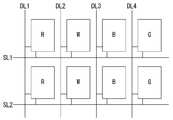
표시패널(10)의 픽셀 어레이에는 입력 영상의 데이터가 표시된다. 표시패널(10)의 픽셀 어레이는 다수의 데이터 라인들(14)과, 데이터 라인들(14)과 교차되는 다수의 스캔 라인들(15), 및 매트릭스 형태로 배치되는 픽셀들을 포함한다. 픽셀들(P) 각각은 컬러 구현을 위하여 적색 서브 픽셀(R), 녹색 서브 픽셀(G), 청색 서브 픽셀(B)로 나뉘어질 수 있고 또한, 도 3과 같이 백색 서브 필터(W)를 더 나뉘어 질 수도 있다. 표시패널(10)에는 픽셀들의 구동 특성 변화량을 센싱하기 위한 레퍼런스 라인들(Reference line)(16)이 형성된다. 도 3에서 DL1~DL4는 데이터 라인들(14)이고, SL1~SL2는 스캔 라인들(15)이다. 서브 픽셀들 각각에는 제1 및 제2 스캔 신호(Scan A, Scan B)가 인가될 수 있도록 한 쌍의 스캔 라인들이 연결될 수 있다.Data of the input image is displayed on the pixel array of the
픽셀의 구동 특성 변화량은 구동 TFT의 문턱 전압 변화량(ΔVth), 이동도 변화량(Δμ) 등과 같은 구동 TFT의 특성 변화를 포함한다. 픽셀의 구동 특성 변화는 서브 필드별 구동 TFT의 소스 전압 변화를 바탕으로 각 컬러별로 센싱될 수 있다.The amount of change in the driving characteristics of the pixel includes a change in the characteristics of the driving TFT such as the amount of change in the threshold voltage (ΔVth) and the amount of change in mobility (Δμ) of the driving TFT. The change in driving characteristics of the pixel may be sensed for each color based on the change in the source voltage of the driving TFT for each subfield.
픽셀들(P) 각각은 도 4와 같이 3 개의 TFT(T1, T2, T3), 하나의 스토리지 커패시터(Cst), 및 OLED를 포함할 수 있으나, 이에 한정되지 않는다. OLED는 도 1과 같이 정공주입층(HIL), 정공수송층(HTL), 발광층(EML), 전자수송층(ETL) 및 전자주입층(EIL) 등이 적층된 유기 화합물층들로 구성될 수 있다. 제1 TFT(T1)는 제1 스캔 펄스(Scan A)에 응답하여 데이터 라인(14)을 통해 입력되는 데이터 전압을 제1 노드(A)를 통해 제2 TFT(T1)의 게이트에 인가한다. 제1 TFT(T1)의 게이트는 제1 스캔 펄스(Scan A)가 인가되는 제1 스캔 라인(15)에 연결된다. 제1 TFT(T1)의 드레인은 데이터 라인(14)에 연결되고, 제1 TFT(T1)의 소스는 제1 노드(A)를 경유하여 제2 TFT(T2)의 게이트에 연결된다. 제2 TFT(T2)는 구동 TFT로서 게이트 전압에 따라 OLED에 흐르는 전류를 조정한다. 제2 TFT(T2)의 드레인에는 고전위 픽셀 전원 전압(VDD)이 인가된다. 제2 TFT(T2)의 소스는 제2 노드(B)를 경유하여 OLED의 애노드에 연결된다. 제3 TFT(T3)는 제2 스캔 펄스(Scan B)에 응답하여 제2 노드(B)와 제3 노드(C)를 연결한다. 제3 노드(C)는 레퍼런스 라인(16)에 연결된다. 제3 TFT(T3)는 픽셀들(P)에 데이터가 기입되는 데이터 인에이블 기간(도 6, AA) 동안 오프(off) 상태를 유지하고, 픽셀들(P)의 서브 픽셀별 구동 특성이 센싱되는 버티컬 블랭크 기간(도 6, VB') 동안 제2 스캔 펄스(Scan B)에 따라 턴-온(turn-on)된다. 제3 TFT(T3)의 드레인은 제2 노드(B)에 연결되고, 그 소스는 제3 노드(C)에 연결된다. 제3 TFT(T3)의 게이트는 제2 스캔 펄스(Scan B)가 인가되는 제2 스캔 라인(15)에 연결된다. 스토리지 커패시터(Cst)는 제1 및 제2 노드(A, B)를 통해 제2 TFT(T2)의 게이트-소스 간에 연결된다. OLED의 애노드는 구동 소자(DRTFT)의 소스에 연결되고, OLED의 캐소드는 기저 전압원(GND)에 연결된다.Each of the pixels P may include three TFTs T1, T2, and T3, one storage capacitor Cst, and an OLED as shown in FIG. 4, but is not limited thereto. OLED may be composed of organic compound layers in which a hole injection layer (HIL), a hole transport layer (HTL), a light emitting layer (EML), an electron transport layer (ETL), and an electron injection layer (EIL) are stacked as shown in FIG. 1. The first TFT T1 applies a data voltage input through the
표시패널 구동회로는 데이터 구동회로(12), 스캔 구동회로(13), 및 타이밍 콘트롤러(Timing controller, 11)를 포함한다. 표시패널 구동회로는 입력 영상의 데이터를 표시패널(10)의 픽셀 어레이에 기입한다.The display panel driving circuit includes a
데이터 구동회로(12)는 하나 이상의 소스 드라이브 IC(integrated circuit)를 포함한다. 데이터 구동회로(12)는 디지털-아날로그 변환기(Digital-to-Analog Converter, 이하 "DAC"라 함)를 이용하여 타이밍 콘트롤러(11)로부터 입력된 입력 영상의 픽셀 데이터(DATA')를 아날로그 감마보상전압으로 변환하여 데이터 전압을 발생하고 그 데이터 전압을 데이터 라인들(14)로 출력한다. 픽셀 데이터 각각은 적색 데이터, 녹색 데이터, 청색 데이터 및 백색 데이터를 포함한다.The
데이터 구동회로(12)는 아날로그-디지털 변환기(Analog-to-Digital Converter, 이하 "ADC"라 함)와 레퍼런스 라인(16)을 통해 수신된 구동 특성 변화 값을 타이밍 콘트롤러(11)에 전송한다. 도 4에 도시된 ADC, DAD 및 스위치(S1)는 데이터 구동회로(12)에 내장된다.The
스캔 구동회로(13)는 타이밍 콘트롤러(11)의 제어 하에 데이터 인에이블 기간 동안 데이터 구동회로(12)의 출력 전압에 동기되는 스캔 펄스(또는 게이트 펄스)를 스캔 라인들(15)에 공급한다. 스캔 구동회로(13)는 버티컬 블랭크 기간(VB') 동안 구동 특성의 변화를 센싱하기 위한 스캔 펄스를 스캔 라인들(15)에 공급한다. 따라서, 스캔 구동회로(13)는 스캔 펄스를 순차적으로 시프트시켜 데이터가 기입되는 픽셀들을 라인 단위로 순차적으로 선택하고 또한, 구동 특성 변화가 센싱될 픽셀들을 라인 단위로 순차적으로 선택한다.The
일반적으로 픽셀의 구동 특성 변화를 1회 센싱하는데 필요한 시간은 1 수평 기간 보다 더 길다. 이에 비하여, 픽셀에 새로운 데이터 전압이 충전하는데 설정된 시간은 1 수평 기간이다. 따라서, 버티컬 블랭크 기간(VB')에서 발생되는 스캔 펄스의 폭은 데이터 인에이블 기간에 발생되는 스캔 펄스 보다 크게 설정된다.In general, the time required to sense a change in driving characteristics of a pixel once is longer than one horizontal period. In contrast, the set time for charging the new data voltage to the pixel is one horizontal period. Accordingly, the width of the scan pulse generated in the vertical blank period VB' is set larger than the scan pulse generated in the data enable period.
타이밍 콘트롤러(11)는 도시하지 않은 호스트 시스템(host system)으로부터 입력 영상의 픽셀 데이터(DATA)와 입력 타이밍 신호들을 입력받는다. 입력 타이밍 신호들은 수직 동기신호(Vsync), 수평 동기신호(Hsync), 데이터 인에이블 신호(DE), 도트 클럭(DCLK) 등을 포함한다. 타이밍 콘트롤러(11)는 입력 영상의 픽셀 데이터와 함께 수신되는 타이밍 신호들(Vsync, Hsync, DE, DCLK)을 바탕으로 데이터 구동회로(12)와 스캔 구동회로(13)의 동작 타이밍을 제어하기 위한 타이밍 제어신호(DDC, GDC)를 발생한다.The
타이밍 콘트롤러(11)는 입력 타이밍 신호에 의해 정의된 데이터 인에이블 기간(AA)을 압축하여 버티컬 블랭크 기간(VB)을 확장하여 1 프레임당 픽셀들의 구동 특성 변화를 센싱할 수 있는 시간을 길게 제어한다. 타이밍 콘트롤러(11)는 프레임 메모리와 라인 메모리를 이용하여 데이터 인에이블 기간(AA)의 주파수를 높임으로써 데이터 인에이블 기간(AA)을 압축하여 상대적으로 서브 픽셀별 구동 특성 변화를 센싱할 수 있는 버티컬 블랭크 기간(VB)을 넓힌다. 타이밍 콘트롤러(11)는 확장된 버티컬 블랭크 기간(VB') 동안 도 5와 같은 신호를 발생하여 데이터 구동회로(12)로 하여금 2 컬러 이상의 서브 픽셀별 구동 특성 변화를 센싱하도록 한다.The
타이밍 콘트롤러(11)는 데이터 구동회로(12)로부터 수신된 구동 특성 변화값을 바탕으로 보상값을 산출하는 화질 보상 알고리즘을 실행한다. 화질 보상 알고리즘은 유기 발광 다이오드 표시장치의 구동 특성 변화를 보상하는 공지의 어떠한 알고리즘으로도 구현될 수 있다. 화질 보상 알고리즘은 보상값으로 입력 영상의 픽셀 데이터(DATA)를 변조한다. 보상값은 픽셀 데이터(DATA)에 가감되어 구동 TFT의 문턱전압을 보상하는 옵셋(offset) 값과, 픽셀 데이터(DATA)에 곱해져 구동 TFT의 이동도를 보상하는 게인(gain) 값을 포함한다. 타이밍 콘트롤러(11)는 화질 보상 알고리즘에 의해 변조된 픽셀 데이터(DATA')를 데이터 구동회로(12)로 전송한다.The
호스트 시스템은 TV(Television) 시스템, 셋톱박스, 네비게이션 시스템, DVD 플레이어, 블루레이 플레이어, 개인용 컴퓨터(PC), 홈 시어터 시스템, 폰 시스템(Phone system) 중 어느 하나로 구현될 수 있다.The host system may be implemented as any one of a TV (Television) system, a set-top box, a navigation system, a DVD player, a Blu-ray player, a personal computer (PC), a home theater system, and a phone system.
본 발명은 타이밍 콘트롤러(11)와 데이터 구동회로(12)를 이용하여 픽셀들의 서브 픽셀별 구동 특성 변화를 보상하는 외부 보상 방법을 적용함으로써 유기 발광 다이오드 표시장치의 수율과 수명을 증가시시킨다. 또한, 본 발명은 외부 보상 방법을 적용하여 픽셀 내의 내부 보상 회로를 생략하거나 최소화함으로써 픽셀들을 도 4와 같이 단순화하여 픽셀의 개구율과 수율을 높일 수 있다.The present invention increases the yield and lifetime of the OLED display by applying an external compensation method for compensating for a change in driving characteristics of each sub-pixel using the
도 4는 픽셀의 등가 회로도이다. 도 5는 구동 특성 변화를 센싱하기 위한 신호들을 보여 주는 파형도이다.4 is an equivalent circuit diagram of a pixel. 5 is a waveform diagram showing signals for sensing a change in driving characteristics.
도 4 및 도 5를 참조하면, 타이밍 콘트롤러(11)는 버티컬 블랭크 기간(VB') 동안 제1 및 제2 스캔 펄스(Scan A, Scan B)와, 초기화 펄스(INIT)를 발생한다. 제1 스캔 펄스(Scan A)의 펄스 폭은 제2 스캔 펄스(Scan B) 보다 작다. 초기화 펄스(INT)의 펄스 폭은 제1 스캔 펄스(Scan A) 보다 크고 제2 스캔 펄스(Scan B) 보다 작다. 제2 스캔 펄스(Scan B)가 라이징(rising)된 후에 초기화 펄스(INIT)와 제1 스캔 펄스(Scan A)가 순차적으로 라이징된다. 이어서, 제1 스캔펄스(Scan A)가 폴링(falling)된 후에 초기화 펄스(INIT)와 제2 스캔 펄스(Scan B)가 순차적으로 폴링된다.4 and 5, the
데이터 구동회로(12)는 버티컬 블랭크 기간(VB') 동안 구동 특성 변화 센싱을 위해 미리 설정된 데이터 전압을 데이터 라인들(14)에 공급한다. 데이터 전압은 입력 영상의 데이터 전압과 무관하게 소정 전압으로 설정된 전압이다.The
제3 TFT(T3)는 제2 스캔 펄스(Scan B)에 응답하여 턴-온되어 제2 및 제3 노드들(B, C)을 연결한다. 이어서, 초기화 펄스(INIT)는 스위치(S1)를 턴-온시켜 소정의 초기화 전압(Vinit)을 제3 노드(C)에 공급한다. 초기화 전압(Vinit)은 제2 및 제3 노드(B, C)를 초기화시킨다. 이어서, 제1 스캔 펄스(Scan A)가 발생되어 소정의 데이터 전압이 제2 TFT(T2)의 게이트에 인가되어 제2 및 제3 노드(B, C)의 전압이 상승한다. ADC는 센싱 시간(ts) 동안 상승하는 제3 노드(C)의 전압 변화를 디지터 값으로 변환하여 구동 특성 변화값을 발생한다. 구동 특성 변화값은 타이밍 콘트롤러(11)에 전송된다.The third TFT T3 is turned on in response to the second scan pulse Scan B to connect the second and third nodes B and C. Subsequently, the initialization pulse INIT turns on the switch S1 to supply a predetermined initialization voltage Vinit to the third node C. The initialization voltage Vinit initializes the second and third nodes B and C. Subsequently, a first scan pulse Scan A is generated so that a predetermined data voltage is applied to the gate of the second TFT T2 to increase the voltages of the second and third nodes B and C. The ADC converts the voltage change of the third node C rising during the sensing time ts into a digit value to generate a driving characteristic change value. The driving characteristic change value is transmitted to the
도 6은 VESA 표준의 디스플레이 타이밍을 보여 주는 파형도이다.6 is a waveform diagram showing the display timing of the VESA standard.
도 6을 참조하면, 입력 타이밍 신호에 의해 정의되는 1 프레임 기간은 데이터 인이이블 구간(AA)과, 버티컬 블랭크 기간(VB)으로 나뉘어진다.Referring to FIG. 6, one frame period defined by an input timing signal is divided into a data enable period AA and a vertical blank period VB.
데이터 인에이블 신호(DE)는 입력 영상의 데이터와 동기된다. 데이터 인에이블 신호(DE)의 1 펄스 주기는 1 수평기간이고, 데이터 인에이블 신호(DE)의 하이 로직(high logic) 구간 즉, 펄스 폭은 1 라인 데이터 타이밍을 나타낸다. 1 수평 기간은 표시패널(100)에서 1 라인의 픽셀들에 데이터를 기입하는데 필요한 시간(horizontal address time)이다.The data enable signal DE is synchronized with the data of the input image. One pulse period of the data enable signal DE is one horizontal period, and a high logic period of the data enable signal DE, that is, a pulse width indicates one line data timing. One horizontal period is a horizontal address time required to write data to one line of pixels in the display panel 100.
데이터 인에이블 신호(DE)와 입력 영상의 데이터는 데이터 인에이블 기간(AA) 동안 입력되고, 버티컬 블랭크 기간(VB)에 입력되지 않는다. 데이터 인에이블 기간(AA)은 픽셀 어레이의 모든 픽셀들에 1 프레임 분량의 픽셀 데이터를 표시하는데 필요한 시간(Vertidcal address time)이다.The data enable signal DE and data of the input image are input during the data enable period AA, and are not input during the vertical blank period VB. The data enable period AA is a time required to display one frame of pixel data in all pixels of the pixel array (Vertidcal address time).
버티컬 블랭크 시간(VB)은 수직 싱크 시간(Vertical sync time, VS), 버티컬 프론트 포치(Vertical Front Porch, FP), 및 버티컬 백 포치(Vertical Back Porch, BP)를 포함한다. 수직 싱크 시간(VS)은 Vsync의 폴링 에지부터 라이징 에지까지의 시간으로서, 한 화면의 시작(또는 끝) 타이밍을 나타낸다.The vertical blank time (VB) includes a vertical sync time (VS), a vertical front porch (FP), and a vertical back porch (BP). The vertical sync time (VS) is the time from the falling edge to the rising edge of Vsync, and represents the start (or end) timing of one screen.
버티컬 프론트 포치(FP)는 1 프레임 데이터의 마지막 라인 데이터 타이밍을 나타내는 데이터 인에이블 신호(DE)의 마지막 펄스의 폴링 에지부터 버티컬 블랭크 시간(VB)의 시작까지의 시간이다. 버티컬 백 포치(BP)는 버티컬 블랭크 시간(VB)의 끝부터 1 프레임 데이터의 제1 라인 데이터 타이밍을 나타내는 데이터 인에이블 신호(DE)의 제1 펄스의 라이징 에지까지의 시간이다.The vertical front porch FP is the time from the falling edge of the last pulse of the data enable signal DE indicating the last line data timing of one frame data to the start of the vertical blank time VB. The vertical back porch BP is a time from the end of the vertical blank time VB to the rising edge of the first pulse of the data enable signal DE indicating the first line data timing of one frame data.
도 6에서 VB'는 타이밍 콘트롤러(11)에 의해 확장된 버티컬 블랭크 기간이고, iDE는 타이밍 콘트롤러(11)에 의해 생성된 내부 데이터 인에이블 신호이다.In FIG. 6, VB' is a vertical blank period extended by the
도 7 및 도 8은 타이밍 콘트롤러(11)를 상세히 보여 주는 블록도들이다.7 and 8 are block diagrams showing the
도 7 및 도 8을 참조하면, 타이밍 콘트롤러(11)는 프레임 메모리(70), 주파수 변환부(72), 알고리즘 실행부(74), 구동회로 제어부(76) 등을 포함한다.7 and 8, the
프레임 메모리(70)는 주파수 변환부(72)에 의해 입력 영상의 픽셀 데이터를 내부 저장 공간에 읽거나 쓴다. 프레임 메모리(70)는 데이터 읽기와 쓰기 동작 과정에서 지연 시간을 줄이기 위하여 2 개의 프레임 메모리(#1, #2)로 구성될 수 있다. 프레임 메모리(70)는 DDR SDRAM(Double data rate synchronous dynamic random access memory)으로 구현될 수 있다.The
주파수 변환부(72)는 쓰기(write) 주파수에 비하여 읽기(read) 주파수가 높은 적어도 2 개의 입력 라인 메모리들(#1, #2)을 이용하여 입력 영상의 데이터 주파수를 높여 데이터 인에이블 기간(AA)을 압축한다.The
주파수 변환부(72)는 도 8과 같이 입력측 라인 메모리들(82), 메모리 제어부(84), 및 출력측 라인 메모리들(86)을 포함한다.The
입력측 라인 메모리들(82)은, 쓰기(write) 주파수에 비하여 읽기(read) 주파수가 높은 제1 및 제2 라인 메모리들(#1, #2)을 포함한다. 출력측 라인 메모리들(86)은 읽기(read) 주파수와 쓰기(write) 주파수가 같은 제1 및 제2 라인 메모리들(#1, #2)을 포함한다.The input-
입력측 라인 메모리들(82 #1, 82 #2)은 데이터 인에이블 신호를 줄이기 위하여 사용된다. 프레임 메모리(70)는 입력측 라인 메모리들(82)을 통해 입력된 1 프레임 분량의 데이터를 빠른 쓰기 속도로 데이터를 저장하여 데이터 인에이블 기간(AA)을 압축한다. 프레임 메모리(70)는 데이터 인에이블 기간(AA)을 압축하여 1 프레임 기간 내에서 상대적으로 버티컬 블랭크 기간(VB)을 늘린다.The input-
출력측 라인 메모리들(84 #1, 84 #2)은 프레임 메모리(70)로부터 픽셀 데이터를 읽어올 때 지연 시간이 발생하는 문제를 방지하기 위하여 이용된다. 만약, 프레임 메모리(70)로부터 픽셀 데이터를 읽어 올 때 시간 지연 문제가 없으면 측력측 라인 메모리들(84)은 생략될 수 있다.The output-
입력측 라인 메모리들(82)의 쓰기 클럭 단자(WRT CLK)에는 제1 주파수의 입력 도트 클럭(DCLK)이 입력된다. 입력측 라인 메모리들(82)의 읽기 클럭 단자(READ CLK)에는 제1 주파수 보다 높은 제2 주파수의 내부 도트 클럭(iDCLK)이 입력된다. 출력측 라인 메모리들(86)의 쓰기 클럭 단자(WRT CLK)와 읽기 클럭 단자(READ CLK)에는 제2 주파수의 내부 도트 클럭(DCLK)이 입력된다.The input dot clock DCLK of the first frequency is input to the write clock terminal WRT CLK of the input-
이하의 실시예에서, 제1 주파수는 80 Mhz로 제2 주파수를 90 Mhz로, 그리고 프레임 메모리(70)의 쓰기 주파수를 736 Mhz로 예시하였으나 이에 한정되지 않는다.In the following embodiments, the first frequency is 80 Mhz, the second frequency is 90 Mhz, and the write frequency of the
입력측 라인 메모리들(82)의 쓰기 클럭 단자(WRT CLK)에는 제1 주파수의 입력 도트 클럭(DCLK)이 입력된다. 입력측 라인 메모리들(82)의 읽기 클럭 단자(READ CLK)에는 제1 주파수 보다 높은 제2 주파수의 내부 도트 클럭(iDCLK)이 입력된다.The input dot clock DCLK of the first frequency is input to the write clock terminal WRT CLK of the input-
메모리 제어부(84)는 입력측 라인 메모리들의 읽기 주파수를 쓰기 주파수 보다 높게 제어하고 입력측 라인 메모리들과 프레임 메모리들의 읽기 및 쓰기 동작 타이밍을 제어한다. 이를 위하여, 메모리 제어부(84)는 입력 도트 클럭 주파수(DCLK)의 주파수 보다 높은 주파수를 갖는 내부 도트 클럭(iDCLK)를 발생하고, 또한 입력 데이터 인에이블 신호(DE)의 주파수 보다 높은 주파수를 갖는 내부 데이터 인에이블 신호(iDE)를 발생한다. 메모리 제어부(84)는 위상동기회로(Phase-Locked Loop, PLL)와 같은 클럭 발생 수단을 이용하여 높은 주파수의 내부 도트 클럭(iDCLK)을 발생한다. 클럭 발생 수단은 내부 발진기(OSC)로부터 입력되는 고속 클럭(OSC CLK)을 소정의 분주비로 분주하여 위상이 고정된 안정한 주파수의 내부 도트 클럭(iDCLK)을 발생한다.The
알고리즘 실행부(74)는 미리 설정된 화질 보상 알고리즘을 실행하여 데이터 구동회로(12)의 ADC를 통해 입력되는 픽셀의 구동 특성 변화량을 보상하기 위한 보상값을 산출한다. 보상값은 구동 TFT(T2)의 문턱 전압 변화량(ΔVth)을 보상하기 위한 옵셋(offset)과, 구동 TFT(T2)의 이동도 변화량(Δμ)을 보상하기 위한 게인(gain) 중 하나 이상을 포함한다. 예컨대, 알고리즘 실행부(74)는 버티컬 블랭크 기간(VB) 동안 구동 TFT(T2)의 이동도 변화를 보상하거나, 구동 TFT(T2)의 문턱 전압 변화와 이동도 변화를 보상할 수 있다.The
구동회로 제어부(76)는 입력 주파수에 비하여 높은 주파수로 발생되는 내부 도트 클럭(iDCLK)과 내부 데이터 인에이블 신호(iDE)를 바탕으로 데이터 구동회로(12)와 스캔 구동회로(13)의 동작 타이밍을 제어하기 위한 타이밍 제어신호(DDC, GDC)를 발생한다.The driving
도 9는 구동 특성 변화의 센싱 시간 확장을 보여 주는 도면이다. 도 10은 본 발명의 센싱 시간 개선 효과를 종래 기술과 비교한 도면이다. 도 10에서, (A)는 종래 기술의 일 예이고, (B)는 본 발명이다.9 is a diagram showing an extension of a sensing time of a change in driving characteristics. 10 is a view comparing the effect of improving the sensing time of the present invention with the prior art. In Figure 10, (A) is an example of the prior art, (B) is the present invention.
도 9 및 도 10을 참조하면, 본 발명은 유기 발광 다이오드 표시장치의 1 프레임 기간에서 데이터 인에이블 기간(AA)을 압축하여 버티컬 블랭크 기간(VB) 내에서 할당되는 센싱 시간을 늘릴 수 있다. 그 결과, 1 버티컬 블랭크 기간(VB) 내에서 1 라인에 포함된 n(n은 2 이상의 양의 정수) 컬러의 서브 픽셀들에서 구동 특성 변화를 센싱할 수 있다. 그 결과, 본 발명은 모든 픽셀들에 대한 서브 픽셀별 구동 특성 변화를 보상하기 위한 보상값들을 빠르게 업데이트하여 구동 특성의 보상 주기를 빠르게 할 수 있다.Referring to FIGS. 9 and 10, according to the present invention, the sensing time allocated within the vertical blank period VB may be increased by compressing the data enable period AA in one frame period of the organic light emitting diode display. As a result, a change in driving characteristics may be sensed in subpixels of n (n is a positive integer equal to or greater than 2) color included in one line within one vertical blank period VB. As a result, according to the present invention, compensation values for compensating for a change in driving characteristics for each sub-pixel for all pixels can be quickly updated to speed up the compensation period of the driving characteristics.
도트 클럭의 주파수를 80 MHz에서 92 MHz로 높일 때 1 수평 기간(1H)의 시간은 3.625us에서 3.15us로 줄어들게 되고 UD 해상도의 라인 수 즉, 2160 line 기준으로 보면 7830us에서 6808.7us로 줄어들게 된다. 데이터 인에이블 신호의 1 펄스 주기에는 290 개의 도트 클럭이 입력된다. 1 프레임 기간을 기준으로 볼 때 도트 클럭의 주파수가 80MHz 일 때 버티컬 블랭크 기간(VB)은 90 수평기간 만큼의 시간인 326.25us 정도이지만 도트 클럭의 주파수를 92 MHz로 높이면 버티컬 블랭크 기간(VB)이 1347.55us로 4배 가량 넓어진다. 그 결과, 본 발명은 1 프레임 기간 마다 4 컬러의 서브 픽셀들 각각의 구동 특성 변화를 센싱할 수 있다.When the frequency of the dot clock is increased from 80 MHz to 92 MHz, the time of one horizontal period (1H) decreases from 3.625us to 3.15us, and the number of lines of UD resolution, that is, 2160 lines, decreases from 7830us to 6808.7us. In one pulse period of the data enable signal, 290 dot clocks are input. Based on one frame period, when the frequency of the dot clock is 80 MHz, the vertical blank period (VB) is about 326.25us, which is about 90 horizontal periods, but if the frequency of the dot clock is increased to 92 MHz, the vertical blank period (VB) becomes It is about 4 times wider to 1347.55us. As a result, the present invention can sense a change in driving characteristics of each of the subpixels of 4 colors every one frame period.
120Hz의 프레임 레이트(frame rate)로 구동하는 표시패널의 해상도가 UD(3840*2160)이고 1 픽셀이 4 개의 서브 픽셀들(R, G, B, W)을 포함할 때, 종래에는 1 버티컬 블랭크 기간(VB)에 1 서브 픽셀에 대한 구동 특성 변화를 센싱할 수 있었다. 종래 기술에서 표시패널의 모든 라인들에서 4 서브 픽셀들의 구동 특성 변화를 센싱하는데 필요한 시간은 4(sub-pixel) * 2160(line) /120(hz) = 72 (sec) 이다. 이에 비하여, 본 발명은 1 버티컬 블랭크 기간(VB)에 4 서브 픽셀에 대한 구동 특성 변화를 센싱할 수 있으므로 표시패널의 모든 라인들에서 4 서브 픽셀들의 구동 특성 변화를 센싱하는데 필요한 시간을 4 (sub-pixel) * 2160 (line) / 120 (Hz) / 4 (회) = 18 (s) 로 줄여 보상 업데이트 시간을 단축할 수 있다.When the resolution of a display panel driven at a frame rate of 120Hz is UD (3840*2160) and 1 pixel includes 4 subpixels (R, G, B, W), conventionally, 1 vertical blank During the period VB, a change in driving characteristics for one sub-pixel could be sensed. In the prior art, a time required to sense a change in driving characteristics of 4 sub-pixels in all lines of a display panel is 4 (sub-pixel) * 2160 (line) /120 (hz) = 72 (sec). In contrast, the present invention can sense the change in driving characteristics of 4 sub-pixels in one vertical blank period (VB), so the time required to sense the change in driving characteristics of 4 sub-pixels in all lines of the display panel is reduced by 4 (sub). -pixel) * 2160 (line) / 120 (Hz) / 4 (times) = 18 (s) to shorten the compensation update time.
도 11은 타이밍 콘트롤러의 주파수 변환 동작 예를 보여 주는 파형도로서 입력측 라인 메모리들(#1, #2)과 프레임 메모리의 읽기 및 쓰기 동작을 보여 준다.11 is a waveform diagram showing an example of a frequency conversion operation of a timing controller, and shows read and write operations of input-side
도 11을 참조하면, 입력측 라인 메모리들(#1, #1)은 메모리 제어부(84)의 제어 하에 입력 영상의 픽셀 데이터(DATA)를 교대로 읽고 쓴다. 입력 도트 클럭(DCLK)이 80 MHz일 경우, 라인 메모리들(#1, #2)은 픽셀 데이터(DAT)를 80 MHz로 쓰고 92 MHz로 읽어 낸다. 프레임 메모리(70)는 메모리 제어부(84)의 제어 하에 92 Mhz의 8배인 736 MHz의 주파수로 라인 메모리들(#1, #2)로부터 교대로 입력되는 픽셀 데이터(DATA)를 쓰고 읽는다.Referring to FIG. 11, input-side
입력측 라인 메모리들(82)은 데이터 인에이블 신호의 주파수를 높이기 위해 이용된다. 제N(N은 양의 정수) 라인의 픽셀 데이터를 Nth Line, 제1 입력측 라인 메모리(82 #1)의 읽기 동작을 Lime mem_in #1 Read, 제1 입력측 라인 메모리(82 #1)의 쓰기 동작을 Lime mem_in #1 Write, 제2 입력측 라인 메모리(82 #2)의 읽기 동작을 Lime mem_in #2 Read, 제2 입력측 라인 메모리(82 #2)의 쓰기 동작을 Lime mem_in #2 Write라 할 때 입력측 라인 메모리들의 동작은 다음과 같다.The input-
Nth Line : Line mem_in #1 Read(92 Mhz), Line mem_in #2 Write(80 Mhz)Nth Line:
(N+1)th line : Line mem_in #1 Write(80 Mhz), Line mem_in #2 Read(92 Mhz)(N+1)th line:
(N+2)th line : Line mem_in #1 Read(92 Mhz), Line mem_in #2 Write(80 Mhz)(N+2)th line:
(N+3)th line : Line mem_in #1 Write(80 Mhz), Line mem_in #2 Read(92 Mhz)(N+3)th line:
프레임 메모리(70)에는 제1 및 제2 입력측 라인 메모리들로부터 픽셀 데이터가 교대로 입력된다. 프레임 메모리(70)는 픽셀 데이터들에 대하여 교대로 읽기 및 쓰기 동작하는 두 개의 프레임 메모리들로 구성될 수 있다. 메모리 제어부(84)는 입력측 라인 메모리들로부터 읽은 픽셀 데이터(DATA)를 두 개의 프레임 메모리들에 교대로 쓴다. 예를 들어, 기수(odd) 번째 프레임 기간 동안 제1 프레임 메모리로부터 픽셀 데이터가 읽혀지고 제2 프레임 메모리에 픽셀 데이터가 쓰여질 수 있다. 이어서, 우수(even) 프레임 기간 제2 프레임 메모리로부터 픽셀 데이터가 읽혀지고 제1 프레임 메모리에 픽셀 데이터가 쓰여질 수 있다.Pixel data is alternately input to the
제N 프레임 기간을 Nth Frame, 제1 프레임 메모리(#1)의 읽기 동작을 DDR #1 Read, 제1 프레임 메모리(#1)의 쓰기 동작을 DDR #1 Write, 제2 프레임 메모리(#2)의 읽기 동작을 DDR #1 Read, 제2 프레임 메모리(#2)의 쓰기 동작을 DDR #2 Write라 할 때 프레임 메모리(70)의 동작은 다음과 같다.The Nth frame period is Nth Frame, the read operation of the first frame memory (#1) is
Nth Frame : DDR #1 Write(736 Mhz), DDR #2 Read(736 Mhz)Nth Frame:
(N+1)th Frame : DDR #1 Read(736 Mhz), DDR #2 Write(736 Mhz)(N+1)th Frame:
(N+2)th Frame : DDR #1 Write(736 Mhz), DDR #2 Read(736 Mhz)(N+2)th Frame:
(N+3)th Frame : DDR #1 Read(736 Mhz), DDR #2 Write(736 Mhz)(N+3)th Frame:
출력측 라인 메모리들(86)은 프레임 메모리(70)로부터 읽혀지는 픽셀 데이터를 일시 저장한다. 출력측 라인 메모리들(86)은 데이터 구동회로(12)에 픽셀 데이터를 끊김 없이 연속적으로 전송하기 위하여 이용된다. 출력측 라인 메모리들(86)은 도 8과 같이 입력측 라인 메모리들(82)의 쓰기 주파수와 같은 주파수로 읽기 및 쓰기 동작한다. 제N 라인의 픽셀 데이터를 Nth Line, 제1 출력측 라인 메모리(86 #1)의 읽기 동작을 Lime mem_out #1 Read, 제1 출력측 라인 메모리(86 #1)의 쓰기 동작을 Lime mem_out #1 Write, 제2 출력측 라인 메모리(86 #2)의 읽기 동작을 Lime mem_out #2 Read, 제2 출력측 라인 메모리(86 #2)의 쓰기 동작을 Lime mem_out #2 Write라 할 때 출력측 라인 메모리들(86)의 동작은 다음과 같다.The output-
Nth Line : Line mem_out #1 Read(92 Mhz), Line mem_out #2 Write(80 Mhz)Nth Line: Line mem_out #1 Read(92 Mhz),
(N+1)th line : Line mem_out #1 Write(92 Mhz), Line mem_out #2 Read(92 Mhz)(N+1)th line:
(N+2)th line : Line mem_out #1 Read(92 Mhz), Line mem_out #2 Write(92 Mhz)(N+2)th line:
(N+3)th line : Line mem_out #1 Write(92 Mhz), Line mem_out #2 Read(92 Mhz)(N+3)th line:
이상 설명한 내용을 통해 당업자라면 본 발명의 기술사상을 일탈하지 아니하는 범위에서 다양한 변경 및 수정이 가능함을 알 수 있을 것이다. 따라서, 본 발명의 기술적 범위는 명세서의 상세한 설명에 기재된 내용으로 한정되는 것이 아니라 특허 청구의 범위에 의해 정하여져야만 할 것이다.
It will be appreciated by those skilled in the art through the above description that various changes and modifications can be made without departing from the technical idea of the present invention. Therefore, the technical scope of the present invention should not be limited to the content described in the detailed description of the specification, but should be determined by the claims.
10 : 표시패널11 : 타이밍 콘트롤러
12 : 데이터 구동회로13 : 스캔 구동회로
70 : 프레임 메모리72 : 주파수 변환부
74 : 알고리즘 실행부76 : 구동회로 제어부
82 : 입력측 라인 메모리들84 : 메모리 제어부
86 : 출력측 라인 메모리들10: display panel 11: timing controller
12: data driving circuit 13: scan driving circuit
70: frame memory 72: frequency converter
74: algorithm execution unit 76: driving circuit control unit
82: input-side line memories 84: memory control unit
86: output side line memories
Claims (6)
Translated fromKorean상기 데이터 인에이블 기간 동안 픽셀 데이터를 데이터 전압으로 변환하여 표시패널의 데이터 라인들에 공급한 후에 확장된 버티컬 블랭크 기간 내에서 상기 표시패널의 구동 특성 변화를 센싱하는 데이터 구동회로;
상기 데이터 인에이블 기간 동안 상기 데이터 전압에 동기되는 스캔 펄스를 스캔 라인들에 공급한 후에 상기 확장된 버티컬 블랭크 기간 내에서 상기 구동 특성의 변화를 센싱하기 위한 스캔 펄스를 출력하는 스캔 구동회로; 및
상기 구동 특성 변화를 바탕으로 설정된 보상값으로 입력 영상의 데이터를 보상하여 상기 데이터 구동회로로 전송하고 상기 데이터 구동회로와 상기 스캔 구동회로의 동작 타이밍을 제어하는 타이밍 콘트롤러를 포함하고,
상기 타이밍 콘트롤러는 입력 타이밍 신호에 의해 정의된 상기 데이터 인에이블 기간을 압축하여 상기 확장된 버티컬 블랭크 기간을 상기 입력 타이밍 신호에 의해 정의된 상기 버티컬 블랭크 기간 보다 길게 제어하며,
상기 확장된 버티컬 블랭크 기간 내에서 발생되는 스캔 펄스의 폭은 상기 데이터 인에이블 기간 내에서 발생되는 스캔 펄스의 폭보다 크고,
상기 스캔 구동회로는 상기 확장된 버티컬 블랭크 기간 내에서 n(n은 2 이상의 양의 정수)개의 스캔 펄스들을 순차적으로 출력하고,
상기 데이터 구동회로는 1 프레임의 확장된 버티컬 블랭크 기간 내에서 상기 표시패널의 1 라인에 포함된 상기 n개의 컬러 서브 픽셀들로부터 구동 특성 변화를 센싱하는, 유기 발광 다이오드 표시장치.In an organic light emitting diode display in which one frame period is divided into a data enable period and a vertical blank period,
A data driving circuit that converts pixel data into a data voltage during the data enable period and supplies it to data lines of the display panel and senses a change in driving characteristics of the display panel within an extended vertical blank period;
A scan driving circuit configured to supply a scan pulse synchronized with the data voltage to the scan lines during the data enable period and then output a scan pulse for sensing a change in the driving characteristic within the extended vertical blank period; And
Compensating the data of the input image with a compensation value set based on the change in the driving characteristic and transmitting the data to the data driving circuit, and a timing controller for controlling the operation timing of the data driving circuit and the scan driving circuit,
The timing controller compresses the data enable period defined by an input timing signal to control the extended vertical blank period to be longer than the vertical blank period defined by the input timing signal,
The width of the scan pulse generated in the extended vertical blank period is greater than the width of the scan pulse generated in the data enable period,
The scan driving circuit sequentially outputs n (n is a positive integer of 2 or more) scan pulses within the extended vertical blank period,
The data driving circuit senses a change in driving characteristics from the n color subpixels included in one line of the display panel within an extended vertical blank period of one frame.
상기 타이밍 콘트롤러는,
상기 표시패널의 1 라인 단위로 교대로 동작하여 1 라인의 픽셀 데이터를 교대로 읽기 및 쓰기하는 제1 및 제2 입력측 라인 메모리들;
상기 표시패널의 1 프레임 기간 단위로 교대로 동작하여 상기 입력측 라인 메모리들로부터 입력되는 데이터읽기 및 쓰기 동작하여 상기 입력측 라인 메모리들로부터 입력되는 데이터를 읽기 및 쓰기하는 제1 및 제2 프레임 메모리들; 및
상기 입력측 라인 메모리들의 읽기 주파수를 상기 입력측 라인 메모리들의 쓰기 주파수 보다 높게 제어하고 상기 입력측 라인 메모리들과 상기 프레임 메모리들의 읽기 및 쓰기 동작 타이밍을 제어하는 메모리 제어부를 포함하는, 유기 발광 다이오드 표시장치.The method of claim 1,
The timing controller,
First and second input-side line memories for alternately reading and writing pixel data of one line by alternately operating in units of one line of the display panel;
First and second frame memories alternately operating in units of one frame period of the display panel to read and write data input from the input-side line memories to read and write data input from the input-side line memories; And
And a memory controller configured to control read frequencies of the input-side line memories higher than write frequencies of the input-side line memories and control timing of read and write operations of the input-side line memories and the frame memories.
상기 타이밍 콘트롤러는,
상기 표시패널의 1 라인 단위로 교대로 동작하여 상기 프레임 메모리들로부터 입력되는 픽셀 데이터를 교대로 읽기 및 쓰기하는 제1 및 제2 출력측 라인 메모리들을 더 포함하고,
상기 메모리 제어부는 상기 입력측 라인 메모리들의 쓰기 주파수와 같은 주파수로 상기 출력측 라인 메모리들의 읽기 및 쓰기 주파수를 제어하는, 유기 발광 다이오드 표시장치.The method of claim 2,
The timing controller,
Further comprising first and second output side line memories for alternately reading and writing pixel data input from the frame memories by alternately operating in units of one line of the display panel,
The memory controller controls read and write frequencies of the output-side line memories at the same frequency as the write frequency of the input-side line memories.
상기 보상값은 픽셀에 내장된 구동 TFT의 문턱 전압 변화량을 보상하기 위한 옵셋 값과, 상기 구동 TFT의 이동도 변화량을 보상하기 위한 게인 값 중 하나 이상을 포함하는, 유기 발광 다이오드 표시장치.The method of claim 1,
The compensation value includes at least one of an offset value for compensating for a change in a threshold voltage of a driving TFT embedded in a pixel and a gain value for compensating for a change in mobility of the driving TFT.
Priority Applications (3)
| Application Number | Priority Date | Filing Date | Title |
|---|---|---|---|
| KR1020130156370AKR102238468B1 (en) | 2013-12-16 | 2013-12-16 | Organic light emitting diode display device |
| US14/552,869US9852695B2 (en) | 2013-12-16 | 2014-11-25 | Organic light emitting diode display capable of extending sensing time and reducing an update cycle |
| CN201410784533.3ACN104715720B (en) | 2013-12-16 | 2014-12-16 | Organic light emitting diode display |
Applications Claiming Priority (1)
| Application Number | Priority Date | Filing Date | Title |
|---|---|---|---|
| KR1020130156370AKR102238468B1 (en) | 2013-12-16 | 2013-12-16 | Organic light emitting diode display device |
Publications (2)
| Publication Number | Publication Date |
|---|---|
| KR20150069804A KR20150069804A (en) | 2015-06-24 |
| KR102238468B1true KR102238468B1 (en) | 2021-04-09 |
Family
ID=53369202
Family Applications (1)
| Application Number | Title | Priority Date | Filing Date |
|---|---|---|---|
| KR1020130156370AActiveKR102238468B1 (en) | 2013-12-16 | 2013-12-16 | Organic light emitting diode display device |
Country Status (3)
| Country | Link |
|---|---|
| US (1) | US9852695B2 (en) |
| KR (1) | KR102238468B1 (en) |
| CN (1) | CN104715720B (en) |
Families Citing this family (36)
| Publication number | Priority date | Publication date | Assignee | Title |
|---|---|---|---|---|
| US9377188B2 (en) | 2013-02-21 | 2016-06-28 | Clearsign Combustion Corporation | Oscillating combustor |
| JP2015156002A (en)* | 2014-02-21 | 2015-08-27 | 三星ディスプレイ株式會社Samsung Display Co.,Ltd. | Display device and control method |
| KR102160814B1 (en)* | 2014-02-24 | 2020-09-29 | 삼성디스플레이 주식회사 | Organic light emitting display device and driving method thereof |
| US20150279267A1 (en)* | 2014-03-28 | 2015-10-01 | Naviance Semiconductor Limited | Phase lock loop based display driver for driving light emitting device and related display apparatus generating internal clock based on external clock |
| KR102192522B1 (en)* | 2014-08-06 | 2020-12-18 | 엘지디스플레이 주식회사 | Organic light emitting display device |
| KR102407981B1 (en)* | 2015-09-18 | 2022-06-13 | 엘지디스플레이 주식회사 | Organic light emitting diode display device |
| US9672765B2 (en)* | 2015-09-30 | 2017-06-06 | Apple Inc. | Sub-pixel layout compensation |
| CN105206225B (en)* | 2015-10-12 | 2017-09-01 | 深圳市华星光电技术有限公司 | OLED gate driver circuitry topologies |
| KR102425237B1 (en)* | 2016-05-31 | 2022-07-26 | 엘지디스플레이 주식회사 | Organic light emitting display device and its driving method |
| CN106297713B (en) | 2016-09-26 | 2020-01-24 | 苏州佳世达电通有限公司 | Display method and display device for improving image dynamic blurring |
| KR102568911B1 (en)* | 2016-11-25 | 2023-08-22 | 삼성디스플레이 주식회사 | Display device and method for driving the same |
| KR102609494B1 (en)* | 2016-11-29 | 2023-12-01 | 엘지디스플레이 주식회사 | Display Device For External Compensation And Driving Method Of The Same |
| CN107945738B (en)* | 2017-11-30 | 2021-02-02 | 上海天马微电子有限公司 | An organic light-emitting display panel and electronic device |
| KR102566790B1 (en)* | 2018-02-12 | 2023-08-16 | 삼성디스플레이 주식회사 | Method of operating a display device supporting a variable frame mode, and the display device |
| KR102490631B1 (en)* | 2018-06-12 | 2023-01-20 | 엘지디스플레이 주식회사 | Organic Light Emitting Display Device And Driving Method Thereof |
| KR102582823B1 (en)* | 2018-07-05 | 2023-09-27 | 삼성디스플레이 주식회사 | Organic light emitting display device and method of driving the same |
| KR102508792B1 (en)* | 2018-08-07 | 2023-03-13 | 엘지디스플레이 주식회사 | Display device |
| KR102655048B1 (en)* | 2018-12-12 | 2024-04-05 | 엘지디스플레이 주식회사 | Electroluminescence display |
| CN109377942B (en) | 2018-12-24 | 2020-07-03 | 合肥鑫晟光电科技有限公司 | Compensation method, device and display device for display device |
| TWI694429B (en) | 2019-01-31 | 2020-05-21 | 友達光電股份有限公司 | Pixel circuit and repair method thereof |
| CN111629263A (en)* | 2020-05-13 | 2020-09-04 | 深圳市华星光电半导体显示技术有限公司 | Display picture compensation method and device, electronic equipment and storage medium |
| CN111627384B (en)* | 2020-05-14 | 2022-09-09 | 深圳市华星光电半导体显示技术有限公司 | Display picture compensation method and device, electronic equipment and storage medium |
| CN111583885B (en) | 2020-06-17 | 2021-11-30 | 京东方科技集团股份有限公司 | Driving method and device of shift register |
| KR102773893B1 (en)* | 2020-07-10 | 2025-02-28 | 삼성디스플레이 주식회사 | Organic light emitting diode display device, and method of sensing a driving characteristic |
| CN111696483B (en)* | 2020-07-10 | 2022-04-08 | 京东方科技集团股份有限公司 | Display panel, driving method thereof and display device |
| KR102792470B1 (en)* | 2020-08-24 | 2025-04-08 | 엘지디스플레이 주식회사 | Display Device And Driving Method Thereof |
| KR102774883B1 (en) | 2020-10-19 | 2025-03-04 | 엘지디스플레이 주식회사 | Electroluminescence Display Device |
| KR20240108577A (en) | 2020-12-09 | 2024-07-09 | 애플 인크. | Displays with reduced temperature luminance sensitivity |
| US11532282B2 (en)* | 2020-12-09 | 2022-12-20 | Apple Inc. | Displays with reduced temperature luminance sensitivity |
| US12205540B2 (en) | 2021-03-18 | 2025-01-21 | Boe Technology Group Co., Ltd. | Shift register unit and driving method thereof, gate driving circuit, and display panel |
| CN112967656B (en)* | 2021-03-26 | 2022-12-20 | 合肥京东方卓印科技有限公司 | Shifting register, grid driving circuit and driving method thereof and display device |
| KR20230057539A (en)* | 2021-10-21 | 2023-05-02 | 삼성디스플레이 주식회사 | Display device |
| CN114265570B (en)* | 2021-12-15 | 2023-06-30 | 深圳市华星光电半导体显示技术有限公司 | Mobility detection method and device, computer equipment and storage medium |
| CN117121084A (en)* | 2022-02-11 | 2023-11-24 | 京东方科技集团股份有限公司 | Display panel, driving method thereof and display device |
| KR20240007854A (en)* | 2022-07-08 | 2024-01-17 | 삼성디스플레이 주식회사 | Display apparatus and method of driving the same |
| US12431069B2 (en)* | 2022-11-01 | 2025-09-30 | Sct Ltd. | Light emitting diode (LED) display driver utilizing ping pong line buffer to reduce hardware costs and latency |
Citations (1)
| Publication number | Priority date | Publication date | Assignee | Title |
|---|---|---|---|---|
| US20130194229A1 (en)* | 2012-02-01 | 2013-08-01 | Synaptics Incorporated | Noise-adapting touch sensing window |
Family Cites Families (21)
| Publication number | Priority date | Publication date | Assignee | Title |
|---|---|---|---|---|
| EP1046110B1 (en)* | 1998-06-30 | 2009-03-18 | Nxp B.V. | Handling of data streams in a memory |
| KR100582204B1 (en)* | 2003-12-30 | 2006-05-23 | 엘지.필립스 엘시디 주식회사 | Memory driving method and apparatus of liquid crystal display device |
| JP3856001B2 (en)* | 2004-01-26 | 2006-12-13 | セイコーエプソン株式会社 | Display controller, display system, and display control method |
| JP5095200B2 (en)* | 2006-12-22 | 2012-12-12 | オンセミコンダクター・トレーディング・リミテッド | Electroluminescence display device and display panel drive device |
| JP5357399B2 (en)* | 2007-03-09 | 2013-12-04 | 株式会社ジャパンディスプレイ | Display device |
| JP2008242323A (en)* | 2007-03-28 | 2008-10-09 | Sanyo Electric Co Ltd | Luminescent display device |
| JP2008250069A (en)* | 2007-03-30 | 2008-10-16 | Sanyo Electric Co Ltd | Electroluminescence display device |
| KR100846969B1 (en)* | 2007-04-10 | 2008-07-17 | 삼성에스디아이 주식회사 | Organic light emitting display device and driving method thereof |
| KR100858616B1 (en)* | 2007-04-10 | 2008-09-17 | 삼성에스디아이 주식회사 | Organic light emitting display device and driving method thereof |
| KR100893482B1 (en)* | 2007-08-23 | 2009-04-17 | 삼성모바일디스플레이주식회사 | Organic light emitting display device and driving method thereof |
| JP2009168927A (en)* | 2008-01-11 | 2009-07-30 | Hitachi Displays Ltd | Organic EL display device |
| KR100902238B1 (en)* | 2008-01-18 | 2009-06-11 | 삼성모바일디스플레이주식회사 | Organic light emitting display device and driving method thereof |
| KR100969769B1 (en)* | 2008-01-21 | 2010-07-13 | 삼성모바일디스플레이주식회사 | Organic light emitting display device and driving method thereof |
| KR101056258B1 (en)* | 2009-09-14 | 2011-08-11 | 삼성모바일디스플레이주식회사 | Organic light emitting display device and driving method thereof |
| CN102884496B (en)* | 2010-02-26 | 2017-06-30 | 辛纳普蒂克斯公司 | Modify demodulation to avoid interference |
| KR101073226B1 (en)* | 2010-03-17 | 2011-10-12 | 삼성모바일디스플레이주식회사 | Organic Light Emitting Display Device |
| US9165518B2 (en)* | 2011-08-08 | 2015-10-20 | Samsung Display Co., Ltd. | Display device and driving method thereof |
| KR101463651B1 (en) | 2011-10-12 | 2014-11-20 | 엘지디스플레이 주식회사 | Organic light-emitting display device |
| KR101938880B1 (en)* | 2011-11-18 | 2019-01-16 | 엘지디스플레이 주식회사 | Organic light emitting diode display device |
| KR101362002B1 (en)* | 2011-12-12 | 2014-02-11 | 엘지디스플레이 주식회사 | Organic light-emitting display device |
| KR101493226B1 (en) | 2011-12-26 | 2015-02-17 | 엘지디스플레이 주식회사 | Method and apparatus for measuring characteristic parameter of pixel driving circuit of organic light emitting diode display device |
- 2013
- 2013-12-16KRKR1020130156370Apatent/KR102238468B1/enactiveActive
- 2014
- 2014-11-25USUS14/552,869patent/US9852695B2/enactiveActive
- 2014-12-16CNCN201410784533.3Apatent/CN104715720B/enactiveActive
Patent Citations (1)
| Publication number | Priority date | Publication date | Assignee | Title |
|---|---|---|---|---|
| US20130194229A1 (en)* | 2012-02-01 | 2013-08-01 | Synaptics Incorporated | Noise-adapting touch sensing window |
Also Published As
| Publication number | Publication date |
|---|---|
| KR20150069804A (en) | 2015-06-24 |
| CN104715720A (en) | 2015-06-17 |
| US20150170578A1 (en) | 2015-06-18 |
| CN104715720B (en) | 2017-06-06 |
| US9852695B2 (en) | 2017-12-26 |
Similar Documents
| Publication | Publication Date | Title |
|---|---|---|
| KR102238468B1 (en) | Organic light emitting diode display device | |
| KR102458078B1 (en) | Gate driving circuit and display device using the same | |
| US10522609B2 (en) | Gate driver circuit, display device using gate driver circuit, and method of driving display device | |
| US10475386B2 (en) | Display panel and electroluminescence display using the same | |
| KR102103241B1 (en) | Organic light emitting diode display device and method of sensing driving characteristics thereof | |
| KR102412107B1 (en) | Luminance control device and display device including the same | |
| US10347173B2 (en) | Organic light emitting diode display and method for driving the same | |
| KR102322708B1 (en) | Organic light emitting diode display device and method of sensing device characteristic | |
| KR102122542B1 (en) | Organic Light Emitting Display Device | |
| KR102450611B1 (en) | Tiled display and optical compensation method thereof | |
| KR20150080198A (en) | Organic light emitting diode display device and driving method the same | |
| KR20210050384A (en) | Display device and driving method thereof | |
| KR102656845B1 (en) | Display device | |
| KR102407981B1 (en) | Organic light emitting diode display device | |
| KR101978781B1 (en) | Display device | |
| KR101720342B1 (en) | Organic Light Emitting Diode Display And Driving Method Thereof | |
| KR102540573B1 (en) | Display panel and display device using the same | |
| KR20190073096A (en) | Electroluminescence display and driving method thereof |
Legal Events
| Date | Code | Title | Description |
|---|---|---|---|
| PA0109 | Patent application | Patent event code:PA01091R01D Comment text:Patent Application Patent event date:20131216 | |
| PG1501 | Laying open of application | ||
| A201 | Request for examination | ||
| PA0201 | Request for examination | Patent event code:PA02012R01D Patent event date:20181112 Comment text:Request for Examination of Application Patent event code:PA02011R01I Patent event date:20131216 Comment text:Patent Application | |
| E902 | Notification of reason for refusal | ||
| PE0902 | Notice of grounds for rejection | Comment text:Notification of reason for refusal Patent event date:20200329 Patent event code:PE09021S01D | |
| E902 | Notification of reason for refusal | ||
| PE0902 | Notice of grounds for rejection | Comment text:Notification of reason for refusal Patent event date:20201025 Patent event code:PE09021S01D | |
| E701 | Decision to grant or registration of patent right | ||
| PE0701 | Decision of registration | Patent event code:PE07011S01D Comment text:Decision to Grant Registration Patent event date:20210129 | |
| GRNT | Written decision to grant | ||
| PR0701 | Registration of establishment | Comment text:Registration of Establishment Patent event date:20210405 Patent event code:PR07011E01D | |
| PR1002 | Payment of registration fee | Payment date:20210405 End annual number:3 Start annual number:1 | |
| PG1601 | Publication of registration | ||
| PR1001 | Payment of annual fee | Payment date:20240315 Start annual number:4 End annual number:4 | |
| PR1001 | Payment of annual fee | Payment date:20250318 Start annual number:5 End annual number:5 |