KR102224422B1 - Processes and apparatus for preparing heterostructures with reduced strain by radial compression - Google Patents
Processes and apparatus for preparing heterostructures with reduced strain by radial compressionDownload PDFInfo
- Publication number
- KR102224422B1 KR102224422B1KR1020157020444AKR20157020444AKR102224422B1KR 102224422 B1KR102224422 B1KR 102224422B1KR 1020157020444 AKR1020157020444 AKR 1020157020444AKR 20157020444 AKR20157020444 AKR 20157020444AKR 102224422 B1KR102224422 B1KR 102224422B1
- Authority
- KR
- South Korea
- Prior art keywords
- substrate
- layer
- dislocations
- central axis
- semiconductor
- Prior art date
- Legal status (The legal status is an assumption and is not a legal conclusion. Google has not performed a legal analysis and makes no representation as to the accuracy of the status listed.)
- Active
Links
- 239000004065semiconductorSubstances0.000claimsabstractdescription62
- 238000000034methodMethods0.000claimsabstractdescription59
- 239000002344surface layerSubstances0.000claimsabstractdescription55
- 238000004519manufacturing processMethods0.000claimsabstractdescription8
- 239000000758substrateSubstances0.000claimsdescription208
- 239000010410layerSubstances0.000claimsdescription128
- 239000000463materialSubstances0.000claimsdescription24
- 230000006835compressionEffects0.000claimsdescription23
- 238000007906compressionMethods0.000claimsdescription23
- 150000002500ionsChemical class0.000claimsdescription21
- 230000002093peripheral effectEffects0.000claimsdescription16
- 238000003825pressingMethods0.000claimsdescription16
- 229910052710siliconInorganic materials0.000claimsdescription14
- 239000010703siliconSubstances0.000claimsdescription14
- 238000010438heat treatmentMethods0.000claimsdescription13
- 238000000151depositionMethods0.000claimsdescription10
- 238000002788crimpingMethods0.000claimsdescription7
- 239000012530fluidSubstances0.000claimsdescription7
- 229910052732germaniumInorganic materials0.000claimsdescription7
- 229910002601GaNInorganic materials0.000claimsdescription6
- JMASRVWKEDWRBT-UHFFFAOYSA-NGallium nitrideChemical compound[Ga]#NJMASRVWKEDWRBT-UHFFFAOYSA-N0.000claimsdescription6
- 230000002040relaxant effectEffects0.000claimsdescription6
- GNPVGFCGXDBREM-UHFFFAOYSA-Ngermanium atomChemical compound[Ge]GNPVGFCGXDBREM-UHFFFAOYSA-N0.000claimsdescription5
- JBRZTFJDHDCESZ-UHFFFAOYSA-NAsGaChemical compound[As]#[Ga]JBRZTFJDHDCESZ-UHFFFAOYSA-N0.000claimsdescription4
- 229910001218Gallium arsenideInorganic materials0.000claimsdescription4
- 229910000530Gallium indium arsenideInorganic materials0.000claimsdescription4
- 229910000577Silicon-germaniumInorganic materials0.000claimsdescription4
- KXNLCSXBJCPWGL-UHFFFAOYSA-N[Ga].[As].[In]Chemical compound[Ga].[As].[In]KXNLCSXBJCPWGL-UHFFFAOYSA-N0.000claimsdescription4
- LEVVHYCKPQWKOP-UHFFFAOYSA-N[Si].[Ge]Chemical compound[Si].[Ge]LEVVHYCKPQWKOP-UHFFFAOYSA-N0.000claimsdescription4
- PMHQVHHXPFUNSP-UHFFFAOYSA-Mcopper(1+);methylsulfanylmethane;bromideChemical compoundBr[Cu].CSCPMHQVHHXPFUNSP-UHFFFAOYSA-M0.000claimsdescription4
- 230000008021depositionEffects0.000claimsdescription4
- 229910052594sapphireInorganic materials0.000claimsdescription4
- 239000010980sapphireSubstances0.000claimsdescription4
- HBMJWWWQQXIZIP-UHFFFAOYSA-Nsilicon carbideChemical compound[Si+]#[C-]HBMJWWWQQXIZIP-UHFFFAOYSA-N0.000claimsdescription4
- 229910010271silicon carbideInorganic materials0.000claimsdescription4
- 238000005488sandblastingMethods0.000claimsdescription2
- 239000013078crystalSubstances0.000abstractdescription14
- 230000007547defectEffects0.000abstractdescription2
- 230000035882stressEffects0.000description12
- 238000000576coating methodMethods0.000description11
- XUIMIQQOPSSXEZ-UHFFFAOYSA-NSiliconChemical compound[Si]XUIMIQQOPSSXEZ-UHFFFAOYSA-N0.000description9
- 125000004429atomChemical group0.000description9
- 239000011248coating agentSubstances0.000description9
- 239000010408filmSubstances0.000description9
- 125000005842heteroatomChemical group0.000description8
- 230000004913activationEffects0.000description6
- 238000000227grindingMethods0.000description6
- 238000002513implantationMethods0.000description6
- 238000005229chemical vapour depositionMethods0.000description5
- 208000035208Ring chromosome 20 syndromeDiseases0.000description4
- 229910021421monocrystalline siliconInorganic materials0.000description4
- -1silicon ionsChemical class0.000description4
- 230000003313weakening effectEffects0.000description4
- 229910021417amorphous siliconInorganic materials0.000description3
- QVGXLLKOCUKJST-UHFFFAOYSA-Natomic oxygenChemical compound[O]QVGXLLKOCUKJST-UHFFFAOYSA-N0.000description3
- 238000004891communicationMethods0.000description3
- 238000007796conventional methodMethods0.000description3
- 238000007373indentationMethods0.000description3
- 239000001301oxygenSubstances0.000description3
- 229910052760oxygenInorganic materials0.000description3
- XKRFYHLGVUSROY-UHFFFAOYSA-NArgonChemical compound[Ar]XKRFYHLGVUSROY-UHFFFAOYSA-N0.000description2
- 230000003213activating effectEffects0.000description2
- 238000000231atomic layer depositionMethods0.000description2
- 230000015572biosynthetic processEffects0.000description2
- 238000005056compactionMethods0.000description2
- 230000008020evaporationEffects0.000description2
- 238000001704evaporationMethods0.000description2
- 230000005669field effectEffects0.000description2
- 239000012212insulatorSubstances0.000description2
- 230000000149penetrating effectEffects0.000description2
- 239000000126substanceSubstances0.000description2
- 239000010409thin filmSubstances0.000description2
- 238000012546transferMethods0.000description2
- 238000000038ultrahigh vacuum chemical vapour depositionMethods0.000description2
- 229910052582BNInorganic materials0.000description1
- 229910016036BaF 2Inorganic materials0.000description1
- PZNSFCLAULLKQX-UHFFFAOYSA-NBoron nitrideChemical compoundN#BPZNSFCLAULLKQX-UHFFFAOYSA-N0.000description1
- 229910004261CaF 2Inorganic materials0.000description1
- OKTJSMMVPCPJKN-UHFFFAOYSA-NCarbonChemical compound[C]OKTJSMMVPCPJKN-UHFFFAOYSA-N0.000description1
- 238000002231Czochralski processMethods0.000description1
- 229910010038TiAlInorganic materials0.000description1
- 238000000137annealingMethods0.000description1
- 229910052786argonInorganic materials0.000description1
- 230000015556catabolic processEffects0.000description1
- 230000001276controlling effectEffects0.000description1
- 238000002109crystal growth methodMethods0.000description1
- 230000003247decreasing effectEffects0.000description1
- 238000006731degradation reactionMethods0.000description1
- 238000001514detection methodMethods0.000description1
- 238000009826distributionMethods0.000description1
- 230000000694effectsEffects0.000description1
- 230000006355external stressEffects0.000description1
- 239000002783friction materialSubstances0.000description1
- 230000014509gene expressionEffects0.000description1
- 229910002804graphiteInorganic materials0.000description1
- 239000010439graphiteSubstances0.000description1
- 229910052734heliumInorganic materials0.000description1
- 239000001307heliumSubstances0.000description1
- SWQJXJOGLNCZEY-UHFFFAOYSA-Nhelium atomChemical compound[He]SWQJXJOGLNCZEY-UHFFFAOYSA-N0.000description1
- 229910052739hydrogenInorganic materials0.000description1
- 239000001257hydrogenSubstances0.000description1
- 125000004435hydrogen atomChemical class[H]*0.000description1
- 239000007943implantSubstances0.000description1
- 238000005468ion implantationMethods0.000description1
- 239000011159matrix materialSubstances0.000description1
- 238000005259measurementMethods0.000description1
- 238000010297mechanical methods and processMethods0.000description1
- 239000012528membraneSubstances0.000description1
- 238000001451molecular beam epitaxyMethods0.000description1
- 229910052754neonInorganic materials0.000description1
- GKAOGPIIYCISHV-UHFFFAOYSA-Nneon atomChemical compound[Ne]GKAOGPIIYCISHV-UHFFFAOYSA-N0.000description1
- 230000007935neutral effectEffects0.000description1
- 238000002360preparation methodMethods0.000description1
- 238000012545processingMethods0.000description1
- 230000001105regulatory effectEffects0.000description1
- 238000005070samplingMethods0.000description1
- 238000007789sealingMethods0.000description1
- 238000001947vapour-phase growthMethods0.000description1
- 229910052724xenonInorganic materials0.000description1
- FHNFHKCVQCLJFQ-UHFFFAOYSA-Nxenon atomChemical compound[Xe]FHNFHKCVQCLJFQ-UHFFFAOYSA-N0.000description1
Images


Classifications
- H—ELECTRICITY
- H01—ELECTRIC ELEMENTS
- H01L—SEMICONDUCTOR DEVICES NOT COVERED BY CLASS H10
- H01L21/00—Processes or apparatus adapted for the manufacture or treatment of semiconductor or solid state devices or of parts thereof
- H01L21/02—Manufacture or treatment of semiconductor devices or of parts thereof
- H01L21/04—Manufacture or treatment of semiconductor devices or of parts thereof the devices having potential barriers, e.g. a PN junction, depletion layer or carrier concentration layer
- H01L21/18—Manufacture or treatment of semiconductor devices or of parts thereof the devices having potential barriers, e.g. a PN junction, depletion layer or carrier concentration layer the devices having semiconductor bodies comprising elements of Group IV of the Periodic Table or AIIIBV compounds with or without impurities, e.g. doping materials
- H01L21/30—Treatment of semiconductor bodies using processes or apparatus not provided for in groups H01L21/20 - H01L21/26
- H01L21/322—Treatment of semiconductor bodies using processes or apparatus not provided for in groups H01L21/20 - H01L21/26 to modify their internal properties, e.g. to produce internal imperfections
- H—ELECTRICITY
- H01—ELECTRIC ELEMENTS
- H01L—SEMICONDUCTOR DEVICES NOT COVERED BY CLASS H10
- H01L21/00—Processes or apparatus adapted for the manufacture or treatment of semiconductor or solid state devices or of parts thereof
- H01L21/67—Apparatus specially adapted for handling semiconductor or electric solid state devices during manufacture or treatment thereof; Apparatus specially adapted for handling wafers during manufacture or treatment of semiconductor or electric solid state devices or components ; Apparatus not specifically provided for elsewhere
- H01L21/683—Apparatus specially adapted for handling semiconductor or electric solid state devices during manufacture or treatment thereof; Apparatus specially adapted for handling wafers during manufacture or treatment of semiconductor or electric solid state devices or components ; Apparatus not specifically provided for elsewhere for supporting or gripping
- H01L21/687—Apparatus specially adapted for handling semiconductor or electric solid state devices during manufacture or treatment thereof; Apparatus specially adapted for handling wafers during manufacture or treatment of semiconductor or electric solid state devices or components ; Apparatus not specifically provided for elsewhere for supporting or gripping using mechanical means, e.g. chucks, clamps or pinches
- H01L21/68714—Apparatus specially adapted for handling semiconductor or electric solid state devices during manufacture or treatment thereof; Apparatus specially adapted for handling wafers during manufacture or treatment of semiconductor or electric solid state devices or components ; Apparatus not specifically provided for elsewhere for supporting or gripping using mechanical means, e.g. chucks, clamps or pinches the wafers being placed on a susceptor, stage or support
- H01L21/68735—Apparatus specially adapted for handling semiconductor or electric solid state devices during manufacture or treatment thereof; Apparatus specially adapted for handling wafers during manufacture or treatment of semiconductor or electric solid state devices or components ; Apparatus not specifically provided for elsewhere for supporting or gripping using mechanical means, e.g. chucks, clamps or pinches the wafers being placed on a susceptor, stage or support characterised by edge profile or support profile
- C—CHEMISTRY; METALLURGY
- C30—CRYSTAL GROWTH
- C30B—SINGLE-CRYSTAL GROWTH; UNIDIRECTIONAL SOLIDIFICATION OF EUTECTIC MATERIAL OR UNIDIRECTIONAL DEMIXING OF EUTECTOID MATERIAL; REFINING BY ZONE-MELTING OF MATERIAL; PRODUCTION OF A HOMOGENEOUS POLYCRYSTALLINE MATERIAL WITH DEFINED STRUCTURE; SINGLE CRYSTALS OR HOMOGENEOUS POLYCRYSTALLINE MATERIAL WITH DEFINED STRUCTURE; AFTER-TREATMENT OF SINGLE CRYSTALS OR A HOMOGENEOUS POLYCRYSTALLINE MATERIAL WITH DEFINED STRUCTURE; APPARATUS THEREFOR
- C30B25/00—Single-crystal growth by chemical reaction of reactive gases, e.g. chemical vapour-deposition growth
- C30B25/02—Epitaxial-layer growth
- C30B25/12—Substrate holders or susceptors
- H—ELECTRICITY
- H01—ELECTRIC ELEMENTS
- H01L—SEMICONDUCTOR DEVICES NOT COVERED BY CLASS H10
- H01L21/00—Processes or apparatus adapted for the manufacture or treatment of semiconductor or solid state devices or of parts thereof
- H01L21/02—Manufacture or treatment of semiconductor devices or of parts thereof
- H01L21/04—Manufacture or treatment of semiconductor devices or of parts thereof the devices having potential barriers, e.g. a PN junction, depletion layer or carrier concentration layer
- H01L21/18—Manufacture or treatment of semiconductor devices or of parts thereof the devices having potential barriers, e.g. a PN junction, depletion layer or carrier concentration layer the devices having semiconductor bodies comprising elements of Group IV of the Periodic Table or AIIIBV compounds with or without impurities, e.g. doping materials
- H01L21/30—Treatment of semiconductor bodies using processes or apparatus not provided for in groups H01L21/20 - H01L21/26
- H01L21/302—Treatment of semiconductor bodies using processes or apparatus not provided for in groups H01L21/20 - H01L21/26 to change their surface-physical characteristics or shape, e.g. etching, polishing, cutting
- H—ELECTRICITY
- H01—ELECTRIC ELEMENTS
- H01L—SEMICONDUCTOR DEVICES NOT COVERED BY CLASS H10
- H01L21/00—Processes or apparatus adapted for the manufacture or treatment of semiconductor or solid state devices or of parts thereof
- H01L21/67—Apparatus specially adapted for handling semiconductor or electric solid state devices during manufacture or treatment thereof; Apparatus specially adapted for handling wafers during manufacture or treatment of semiconductor or electric solid state devices or components ; Apparatus not specifically provided for elsewhere
- H01L21/67005—Apparatus not specifically provided for elsewhere
- H01L21/67011—Apparatus for manufacture or treatment
- H01L21/67092—Apparatus for mechanical treatment
- H—ELECTRICITY
- H01—ELECTRIC ELEMENTS
- H01L—SEMICONDUCTOR DEVICES NOT COVERED BY CLASS H10
- H01L21/00—Processes or apparatus adapted for the manufacture or treatment of semiconductor or solid state devices or of parts thereof
- H01L21/67—Apparatus specially adapted for handling semiconductor or electric solid state devices during manufacture or treatment thereof; Apparatus specially adapted for handling wafers during manufacture or treatment of semiconductor or electric solid state devices or components ; Apparatus not specifically provided for elsewhere
- H01L21/683—Apparatus specially adapted for handling semiconductor or electric solid state devices during manufacture or treatment thereof; Apparatus specially adapted for handling wafers during manufacture or treatment of semiconductor or electric solid state devices or components ; Apparatus not specifically provided for elsewhere for supporting or gripping
- H01L21/6838—Apparatus specially adapted for handling semiconductor or electric solid state devices during manufacture or treatment thereof; Apparatus specially adapted for handling wafers during manufacture or treatment of semiconductor or electric solid state devices or components ; Apparatus not specifically provided for elsewhere for supporting or gripping with gripping and holding devices using a vacuum; Bernoulli devices
- H—ELECTRICITY
- H01—ELECTRIC ELEMENTS
- H01L—SEMICONDUCTOR DEVICES NOT COVERED BY CLASS H10
- H01L21/00—Processes or apparatus adapted for the manufacture or treatment of semiconductor or solid state devices or of parts thereof
- H01L21/67—Apparatus specially adapted for handling semiconductor or electric solid state devices during manufacture or treatment thereof; Apparatus specially adapted for handling wafers during manufacture or treatment of semiconductor or electric solid state devices or components ; Apparatus not specifically provided for elsewhere
- H01L21/683—Apparatus specially adapted for handling semiconductor or electric solid state devices during manufacture or treatment thereof; Apparatus specially adapted for handling wafers during manufacture or treatment of semiconductor or electric solid state devices or components ; Apparatus not specifically provided for elsewhere for supporting or gripping
- H01L21/687—Apparatus specially adapted for handling semiconductor or electric solid state devices during manufacture or treatment thereof; Apparatus specially adapted for handling wafers during manufacture or treatment of semiconductor or electric solid state devices or components ; Apparatus not specifically provided for elsewhere for supporting or gripping using mechanical means, e.g. chucks, clamps or pinches
- H01L21/68714—Apparatus specially adapted for handling semiconductor or electric solid state devices during manufacture or treatment thereof; Apparatus specially adapted for handling wafers during manufacture or treatment of semiconductor or electric solid state devices or components ; Apparatus not specifically provided for elsewhere for supporting or gripping using mechanical means, e.g. chucks, clamps or pinches the wafers being placed on a susceptor, stage or support
- H01L21/6875—Apparatus specially adapted for handling semiconductor or electric solid state devices during manufacture or treatment thereof; Apparatus specially adapted for handling wafers during manufacture or treatment of semiconductor or electric solid state devices or components ; Apparatus not specifically provided for elsewhere for supporting or gripping using mechanical means, e.g. chucks, clamps or pinches the wafers being placed on a susceptor, stage or support characterised by a plurality of individual support members, e.g. support posts or protrusions
Landscapes
- Engineering & Computer Science (AREA)
- Physics & Mathematics (AREA)
- Condensed Matter Physics & Semiconductors (AREA)
- General Physics & Mathematics (AREA)
- Manufacturing & Machinery (AREA)
- Computer Hardware Design (AREA)
- Microelectronics & Electronic Packaging (AREA)
- Power Engineering (AREA)
- Chemical & Material Sciences (AREA)
- General Chemical & Material Sciences (AREA)
- Chemical Kinetics & Catalysis (AREA)
- Crystallography & Structural Chemistry (AREA)
- Materials Engineering (AREA)
- Metallurgy (AREA)
- Organic Chemistry (AREA)
- Recrystallisation Techniques (AREA)
- Container, Conveyance, Adherence, Positioning, Of Wafer (AREA)
- Crystals, And After-Treatments Of Crystals (AREA)
- Chemical Vapour Deposition (AREA)
- Semiconductor Lasers (AREA)
Abstract
Translated fromKoreanDescription
Translated fromKorean[관련 출원에 대한 상호참조][Cross reference to related applications]
본 출원은 2012년 12월 31일 출원된 미국 가출원 번호 제61/747,613호; 2013년 3월 15일 출원된 미국 가출원 번호 제61/793,999호; 2013년 3월 15일 출원된 미국 가출원 번호 제61/790,445호; 및 2013년 3월 15일 출원된 미국 가출원 번호 제61/788,744호의 혜택을 주장하며, 이 출원들의 각각은 참조에 의해 본 명세서에 통합된다.This application is filed on December 31, 2012, filed in US Provisional Application No. 61/747,613; US Provisional Application No. 61/793,999, filed March 15, 2013; US Provisional Application No. 61/790,445, filed March 15, 2013; And US Provisional Application No. 61/788,744, filed March 15, 2013, each of which is incorporated herein by reference.
본 개시는 감소된 변형(strain)을 가진 반도체 이종구조들(semiconductor heterostructures)의 제조와 일반적으로 관련되는데, 특히 자신과는 상이한 결정 격자 상수를 갖는 표면 층에 맞추어지고 그에 의해 비교적 낮은 결함의 이종구조를 형성하는 반도체 기판을 가진 이종구조들과 관련된다.The present disclosure relates generally to the fabrication of semiconductor heterostructures with reduced strain, in particular a heterostructure of relatively low defects tailored to a surface layer having a crystal lattice constant different from itself. Is related to heterogeneous structures having a semiconductor substrate forming a.
디바이스 성질 표면을 가진 디바이스 층 및 디바이스 층의 물질과 상이한 결정 격자 구조를 갖는 기판을 포함하는 다층 구조들(multi-layered structures)이 수많은 상이한 목적들을 위해 유용하다. 이들 다층 구조들은 달라지는 격자 상수들을 갖는 물질로 된 다중 층을 전형적으로 포함한다. 층들 간의 격자 부정합(lattice mismatch)은 층들이 변형되도록 한다. 불일치 전위들(misfit dislocations)이 층들 간의 변형을 릴랙스하기 위해 디바이스 층에 자발적으로 형성될 수 있다. 그와 같은 전위들은 다중 층 반도체 구조의 품질과 유용성을 저하시킨다.Multi-layered structures including a device layer having a device property surface and a substrate having a crystal lattice structure different from the material of the device layer are useful for a number of different purposes. These multilayer structures typically include multiple layers of materials with varying lattice constants. A lattice mismatch between the layers causes the layers to deform. Misfit dislocations may spontaneously form in the device layer to relax the strain between the layers. Such dislocations degrade the quality and usefulness of the multilayer semiconductor structure.
격자 부정합된 반도체 층들 간의 변형을 릴랙스하기 위한 방법들과 실질적으로 전위들이 없는 기판들 및 디바이스 층들이 달성되는 방법들에 대한 지속적 필요가 존재한다.There is a continuing need for methods for relaxing strain between lattice mismatched semiconductor layers and for methods in which substrates and device layers substantially free of dislocations are achieved.
본 개시의 한 양태는 기판, 기판 상에 배치되는 표면 층 및 기판과 표면 층 간의 계면을 포함하는 이종구조에서 변형을 릴랙스하기 위한 공정을 지향한다. 기판은 중앙 축, 중앙 축에 전반적으로 수직인 후면, 및 중앙 축을 통과하여 기판을 가로질러 연장하는 직경을 포함한다. 전위 소스 층(dislocation source layer)이 기판에 형성된다. 기판은, 전위를 발생하고 또한 전위 소스 층으로부터 표면 층을 향하여 전위들을 미끄러지게(glide) 하기 위해 방사상으로 압착(compress)된다.One aspect of the present disclosure is directed to a process for relaxing strain in a heterostructure comprising a substrate, a surface layer disposed on the substrate, and an interface between the substrate and the surface layer. The substrate includes a central axis, a rear surface generally perpendicular to the central axis, and a diameter extending through the central axis and across the substrate. A dislocation source layer is formed on the substrate. The substrate is radially compressed to generate dislocations and also to glide dislocations from the dislocation source layer toward the surface layer.
본 개시의 또 다른 양태는 릴랙스된 이종구조를 제조하기 위한 공정을 지향한다. 표면 층은 반도체 기판의 전면 상에 피착되고, 그에 의해 표면 층과 기판 간의 변형을 생성한다. 전위 소스 층이 기판에 형성된다. 표면 층과 기판에서의 변형은, 전위들(dislocations)을 발생하고 또한 전위 소스 층으로부터 표면 층을 향하여 전위들을 미끄러지게 하기 위해 기판을 방사상으로 압착함으로써 릴랙스된다.Another aspect of the present disclosure is directed to a process for manufacturing a relaxed heterostructure. The surface layer is deposited on the front surface of the semiconductor substrate, thereby creating a strain between the surface layer and the substrate. A potential source layer is formed on the substrate. Deformation in the surface layer and substrate is relaxed by radially pressing the substrate to generate dislocations and also slide dislocations from the dislocation source layer toward the surface layer.
본 개시의 또 다른 양태는 장치에서 반도체 구조를 방사상으로 압착하기 위한 방법을 지향한다. 구조는 전면, 후면 및 원주 둘레(circumferential edge)를 갖는다. 장치는 구조의 원주 둘레에 인접하여 구조와 접촉하기 위한 최상부 판 및 후방 판을 포함하는 구조 홀더(structure holder)를 포함한다. 최상부 판은 구조의 전면과 접촉하도록 적응되고 후방 판은 구조의 후면과 접촉하기 위해 적응된다. 주위 챔버(peripheral chamber)가 최상부 판, 후방 판 및 구조의 원주 둘레 간에 형성된다. 주위 챔버에서의 압력은 방사상으로 구조를 압착하기 위해 변화된다.Another aspect of the present disclosure is directed to a method for radially compressing a semiconductor structure in a device. The structure has a front, a back and a circumferential edge. The device includes a structure holder including a top plate and a rear plate for contacting the structure adjacent to the circumference of the structure. The top plate is adapted to contact the front side of the structure and the rear plate is adapted to contact the rear side of the structure. A peripheral chamber is formed between the top plate, the rear plate and the circumference of the structure. The pressure in the surrounding chamber is changed to radially compress the structure.
도 1은 실리콘 이종구조의 개략 단면도이다;
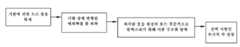
도 2는 이종구조를 제조하기 위한 공정을 묘사하는 흐름도이다;
도 3-4는 반도체 구조 및 반도체 구조를 압착하기 위한 구조 홀더의 단면도들이다;
도 5는 반도체 구조 및 반도체 구조를 압착하기 위한 구조 홀더의 또 다른 실시예의 단면도들이다;
도 6-7은 그 위의 코팅 및 도 3의 구조 홀더를 갖는 반도체 구조의 단면도들이다;
도 8은 반도체 구조 및 이 구조를 그 가운데 탑재된 도 3의 구조 홀더에 의해 압착하기 위한 장치의 개략 단면도이다;
도 9는 반도체 구조 및 반도체 구조를 압착하기 위한 구조 홀더의 또 다른 실시예의 단면도들이다;
도 10은 복수의 반도체 구조 및 반도체 구조들을 압착하기 위한 구조 홀더의 단면도이다;
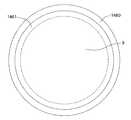
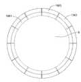
도 11은 반도체 구조를 압착하기 위한 구조 홀더의 또 다른 실시예의 평면도이다;
도 12는 반도체 구조 및 반도체 구조를 압착하기 위한 구조 홀더의 또 다른 실시예의 단면도이다;
도 13은 그루브를 갖는 반도체 구조 및 반도체 구조를 압착하기 위한 구조 홀더의 또 다른 실시예의 단면도이다;
도 14는 반도체 구조 및 최상부 판을 가진 도 13의 구조 홀더의 단면도이다;
도 15는 2개의 그루브를 갖는 반도체 구조 및 반도체 구조를 압착하기 위한 구조 홀더의 또 다른 실시예의 단면도이다;
도 16은 반도체 구조 및 압착부를 포함하는 구조 홀더의 또 다른 실시예의 단면도이다;
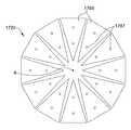
도 17은 반도체 구조 및 도 16의 구조 홀더의 평면도이다;
도 18은 구조 홀더 및 세그먼트들을 갖는 구조 홀더의 또 다른 실시예의 평면도이다; 및
도 19는 반도체 구조 및 플랜지를 갖는 구조 홀더의 또 다른 실시예의 단면도이다.
대응하는 참조 번호들은 도면의 전체에 걸쳐서 대응하는 부분들을 표시한다.1 is a schematic cross-sectional view of a silicon heterostructure;
2 is a flow chart depicting a process for manufacturing a heterostructure;
3-4 are cross-sectional views of a semiconductor structure and a structure holder for pressing the semiconductor structure;
5 are cross-sectional views of a semiconductor structure and another embodiment of a structure holder for pressing the semiconductor structure;
6-7 are cross-sectional views of a semiconductor structure with a coating thereon and the structure holder of FIG. 3;
Fig. 8 is a schematic cross-sectional view of a semiconductor structure and an apparatus for pressing the structure by the structure holder of Fig. 3 mounted therein;
9 are cross-sectional views of a semiconductor structure and another embodiment of a structure holder for pressing the semiconductor structure;
10 is a cross-sectional view of a plurality of semiconductor structures and a structure holder for compressing semiconductor structures;
11 is a plan view of another embodiment of a structural holder for compressing a semiconductor structure;
12 is a cross-sectional view of another embodiment of a semiconductor structure and a structure holder for pressing the semiconductor structure;
13 is a cross-sectional view of another embodiment of a semiconductor structure having a groove and a structure holder for pressing the semiconductor structure;
14 is a cross-sectional view of the structural holder of FIG. 13 with a semiconductor structure and a top plate;
15 is a cross-sectional view of another embodiment of a semiconductor structure having two grooves and a structure holder for pressing the semiconductor structure;
16 is a cross-sectional view of another embodiment of a structural holder including a semiconductor structure and a crimp portion;
Fig. 17 is a plan view of the semiconductor structure and the structure holder of Fig. 16;
18 is a plan view of another embodiment of a structural holder and a structural holder with segments; And
19 is a cross-sectional view of another embodiment of a structural holder having a semiconductor structure and a flange.
Corresponding reference numbers indicate corresponding parts throughout the drawing.
본 개시의 하나 이상의 양태들에 따라서, 기판과 기판과는 상이한 격자 상수를 갖는 표면 층 사이의 감소된 변형을 가진 이종구조들은 도 2의 공정에 의해서 그런 것처럼 제조될 수 있다. 표면 층은 또한 "에피택셜 층", "헤테로에피택셜 층(heteroepitaxial layer)", "피착 막", “막", "헤테로 층(heterolayer)" 또는 "피착 층"으로서 본 명세서에서 지칭될 수 있다. 실질적으로 릴랙스된 표면 층을 가지고 또한 관통 전위(threading dislocation)들로도 불리는 불일치 전위들의 감소된 농도를 달성하는 이종구조가 형성될 수 있다.In accordance with one or more aspects of the present disclosure, heterostructures with reduced strain between a substrate and a surface layer having a different lattice constant than the substrate may be fabricated as such by the process of FIG. 2. The surface layer may also be referred to herein as “epitaxial layer”, “heteroepitaxial layer”, “deposited film”, “film”, “heterolayer” or “deposited layer” A heterostructure can be formed that has a substantially relaxed surface layer and achieves a reduced concentration of mismatch dislocations, also called threading dislocations.
일반적으로, 본 개시의 공정들은 반도체 기판에 전위 소스 층을 형성하는 단계, 전위 소스 층의 형성 전후에 기판 상에 헤테로 층을 피착하는 단계 및 전위들을 발생하고(즉, 활성화하고) 또한 전위 소스 층으로부터 표면 층을 향하여 전위들을 미끄러지게 하기 위해 이종구조를 방사상으로 압착하는 단계를 포함할 수 있다. 소스 층의 활성화 및 소스 층으로부터 피착 층과의 계면을 향하는 전위들의 미끄러짐은 압착을 기판에 가함으로써 병행적으로 발생한다. 변형력은 전위들을 활성화하고 미끄러지게 하기 위해 하나 이상의 단계들 및 다양한 조합들로 가해질 수 있으며, 그에 의해 이종구조를 소성적으로(plastically) 압착한다.In general, the processes of the present disclosure include forming a potential source layer on a semiconductor substrate, depositing a hetero layer on the substrate before and after formation of the potential source layer, and generating (i.e., activating) dislocations, and It may include radially compressing the heterostructure to slide dislocations from and towards the surface layer. The activation of the source layer and the sliding of dislocations from the source layer toward the interface with the deposited layer occurs in parallel by applying compression to the substrate. The strain can be applied in one or more steps and in various combinations to activate and slide dislocations, thereby plastically compressing the heterostructure.
헤테로 층은 기판의 표면 상에 막을 형성하기 위해, 기판의 본래 결정 격자 상수 aS와는 다른 결정 격자 상수 aSI를 가질 수 있다. 일반적으로, 헤테로 층의 결정 격자 상수 aSI는 기판의 본래 결정 격자 상수 aS 보다 작아서, 압착에 의한 기판에서의 전위 루프(dislocation loop)들의 발생과 미끄러짐을 제어함으로써 기판이 소성적으로 응력 변형되고 또한 막의 결정 격자와 더 적절하게 정렬되고, 그에 의해 막이 완전히 릴랙스되고 또한 기판상에서 감소된 밀도의 관통 전위들을 갖도록 허용하게 된다.The hetero layer may have a crystal lattice constant aSIdifferent from the original crystal lattice constant a S of the substrate to form a film on the surface of the substrate. In general, the crystal lattice constant aSI of the hetero layer is smaller than the original crystal lattice constant aS of the substrate, so that the substrate is plastically strained by controlling the occurrence and slippage of dislocation loops in the substrate by compression. It is also more properly aligned with the crystal lattice of the film, thereby allowing the film to be completely relaxed and also to have a reduced density of through dislocations on the substrate.
본 개시의 방법들은 헤테로 층들을 릴랙스하는데 있어서 종래의 방법들을 능가하는 여러 장점들을 갖는다. 종래의 방법들은 막과 기판 간에 응력들에서의 큰 비대칭성을 생성하는데, 이는 응력들이 최대인 곳, 즉 막에서의 전위 발생으로 이어진다. 전위 루프들을 막에 한정하게 됨으로써, 전위들은 열화 관통 전위들의 역할을 하는 세그먼트들을 뒤에 남긴다. 그와 같은 관통 전위들의 밀도를 최소화하기를 시도하는 많은 노력들이 기울여졌다.The methods of the present disclosure have several advantages over conventional methods in relaxing hetero layers. Conventional methods create a large asymmetry in stresses between the film and the substrate, which leads to where the stresses are maximum, ie dislocations in the film. By confining dislocation loops to the membrane, dislocations leave behind segments that serve as degradation through dislocations. Much effort has been made to try to minimize the density of such penetrating dislocations.
대조적으로, 본 개시의 방법들은 (예를 들어, 기판을 약화(weakening)시키고 또한 기판을 약화시키는 동안 그 가운데에서 전위 발생을 피하기 위해 상대적으로 얇은 막을 이용함으로써) 전위 발생이 기판에서 생기도록 하면서 응력들의 비대칭성을 낳게 된다. 이것은 기판과 막 사이의 계면에 불일치 전위 층을 형성하는 동안 전위들이 기판에 한정되도록 허용한다. 다양한 제어된 방식들로 전위들을 도입함으로써 기판을 약화시키면, 외부 변형력(external stress)들이 전위들을 활성화하기 위해 시스템에 가해질 수 있다. 이것은 상대적으로 큰 고유의 내부 응력(internal stress)로 인한 자가 릴랙세이션(즉, 외부 변형력들의 가해짐이 없는 릴랙세이션)을 낳는 종래 방법들과 다르다. 본 개시의 방법들은 상대적으로 얇은 막으로 적절한 온도들에서 약화 및 외부 변형력의 가함에 의해 자가 릴랙세이션에 의하는 것과는 다른 릴랙세이션을 수반하여, 자가 릴랙세이션이 발생하지 않도록 한다.In contrast, the methods of the present disclosure (e.g., by weakening the substrate and also by using a relatively thin film to avoid dislocations occurring in the middle of the substrate while weakening the substrate) allow the generation of dislocations to occur in the substrate while stress It leads to the asymmetry of people. This allows dislocations to be confined to the substrate while forming the mismatch dislocation layer at the interface between the substrate and the film. When weakening the substrate by introducing dislocations in various controlled ways, external stresses can be applied to the system to activate dislocations. This differs from conventional methods that result in self-relaxation (ie, relaxation without the application of external strains) due to a relatively large inherent internal stress. The methods of the present disclosure entail a relaxation different from that by self-relaxation by applying a weakening and external straining force at appropriate temperatures with a relatively thin film, so that self-relaxation does not occur.
I.I.반도체 기판Semiconductor substrate
도 1을 참조하면, 반도체 기판(1)은 CVD(chemical vapor deposition)에 의한 에피택셜 층의 피착에 의해서와 같은 표면 층을 지지하기 위한 기판으로 사용하는 데에 적합한 임의의 단결정 반도체 물질일 수 있다. 일반적으로, 반도체 기판은 실리콘, 탄화 실리콘, 사파이어, 게르마늄, 실리콘 게르마늄, 질화 갈륨, 질화 알루미늄, 갈륨 비소, 인듐 갈륨 비소 또는 이것들의 임의의 조합으로 이루어진 군으로부터 선택되는 물질로 구성될 수 있다. 전형적으로, 반도체 기판은 실리콘으로 구성된다.Referring to FIG. 1, the
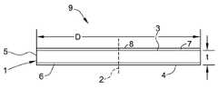
반도체 기판(1)은 이하에 보다 상세하게 설명되는 바와 같이 표면 층을 피착하기 위한 기판으로서의 용도 및 기판 물질에 변형력을 가하기에 적합한 것의 두 가지에 알맞은 임의의 형태를 가질 수 있다. 전형적으로, 반도체 기판은 중앙 축(2); 피착 층(7)과의 계면(3) 및 후면(4) - 여기서 기판-표면 층 계면(3) 및 후면(4)은 전반적으로 중앙 축(2)과 수직임 - ; 계면으로부터 기판의 후면까지의 거리에 대응하는 두께 t; 원주 둘레(5); 및 중앙 축을 통과하며 기판을 가로질러 연장하는 직경 D를 갖는다. 예시 목적을 위해, 후면(4)은 전위 소스 층이 형성될 곳에서의 또는 그 부근에서의 대향 면으로서 기술될 것이고 이와 같이 본 명세서에서 "대향 면(opposing surface)" 및/또는 "손상된 면"으로서 지칭될 수 있다는 것을 유의해야 한다. 이와 관련하여, 이하에 기술되는 이종구조 자체 및 피착 층(7)은 일반적으로 기판(1)과 동심원을 이루고, 또한 중앙 축(2); 원주 둘레(5); 및 이종구조(및 또한 표면 층)를 가로질러 그리고 중앙 축을 통하여 연장하는 직경 D를 갖는다.The
기판(1)은 반도체 층이 그 상에 피착될 기판으로 사용되기 위한 임의의 적절한 직경을 가질 수 있다. 일반적으로, 기판(1)은 약 150㎜ 이상의 직경을 갖는다. 전형적으로, 기판(1)은 약 200㎜ 이상, 약 300㎜ 이상 또는 심지어 약 450㎜ 이상의 직경을 갖는다. 기판 직경이 소성적으로 이종구조를 변형시키기 전의 직경일 수 있고, 그런 경우에 직경은 이하에서 더욱 상세히 논의되는 것처럼 소성 응력 변형 후에 표명된 값들로부터 증가하거나 감소할 수 있다는 것을 유의해야 한다. 대안적으로, 소성 응력 변형 전의 기판은 표명된 값들보다 작거나 또는 큰 직경을 가질 수 있어서 소성 응력 변형 후의 직경이 표명된 값들과 대략 동일하도록 될 수 있다.The
유사하게, 기판(1)은 반도체 층이 그 상에 피착될 수 있는 기판으로 사용하는 데에 적절한 임의의 두께, t를 가질 수 있다. 예를 들어, 기판은 약 500 미크론으로부터 약 1000 미크론까지의, 전형적으로 약 600 미크론으로부터 약 1000 미크론까지의, 약 700 미크론으로부터 약 1000 미크론까지의, 약 700 미크론으로부터 약 900 미크론까지의 또는 심지어 약 700 미크론으로부터 약 800 미크론까지의 두께, t를 가질 수 있다.Similarly, the
몇몇 실시예들에서, 예를 들어, 기판(1)은 약 150㎜ 이상, 약 200㎜ 이상, 약 300㎜ 이상 또는 심지어 약 450㎜ 이상의 직경과 약 675 미크론으로부터 약 1000 미크론까지의 또는 심지어 약 725 미크론으로부터 약 925 미크론까지의 두께를 갖는, 초크랄스키 결정 성장 방법들에 의해 성장된 단결정 실리콘 잉곳으로부터 슬라이싱(slice)된 단결정 실리콘 웨이퍼일 수 있다.In some embodiments, for example, the
에피택셜 층이 그 상에 피착되는 기판 표면은 에피택셜 층을 피착하는데 적합하도록 연마 처리(polish)될 수 있거나 또는 CVD 전에 추가로 조절될 수 있다. 대향 면이 또한 연마 처리될 수 있거나 또는 대안적으로 본 개시의 범위에서 벗어나지 않고서 비 연마 처리될 수 있는데, 즉 연삭되는 것으로서(as-ground), 래핑되는 것으로서(as-lapped) 또는 래핑되고 에칭되는 것으로서 처리될 수 있다. 다양한 실시예들에서, 대향 면은 비 연마된 상태로 남겨질 수 있는데, 여기서 연삭되거나, 래핑되거나 또는 래핑되고 에칭되는 표면은 전위 소스 층으로서 활용될 수 있다. 대안적으로 또는 덧붙여, 대향 면은 손상되어 이하에 보다 상세하게 설명된 바와 같은 전위 소스 층을 형성할 수 있다.The substrate surface on which the epitaxial layer is deposited may be polished to suit the deposition of the epitaxial layer or may be further adjusted prior to CVD. The opposite side may also be polished or alternatively may be non-polished without departing from the scope of the present disclosure, i.e. as-ground, as-lapped or wrapped and etched. Can be treated as. In various embodiments, the opposite side may be left unpolished, wherein the surface to be ground, wrapped or wrapped and etched may be utilized as a potential source layer. Alternatively or in addition, the opposite side may be damaged to form a potential source layer as described in more detail below.
초크랄스키 성장된 실리콘이 전형적으로 약 5x10¹⁷ 내지 약 9x10¹⁷atoms/cm3(ASTM 표준 F-121-83)의 범위 내의 산소 농도를 갖는다는 것을 유의해야 한다. 일반적으로, 본 개시에서 기판에 사용되는 단결정 실리콘 웨이퍼는, 산소 농도가 전위의 활성화와 미끄러짐을 막을 만큼 그렇게 과도하지만 않다면, 초크랄스키 공정에 의해 전형적으로 획득 가능한 범위 내의 또는 심지어 그 범위를 벗어난 어떤 값이 되는 산소 농도를 가질 것이다.It should be noted that Czochralski grown silicon typicallyhas an oxygen concentration in the range of about 5x10 17 to about 9x10¹⁷ atoms/cm3 (ASTM standard F-121-83). In general, the single crystal silicon wafer used in the substrate in the present disclosure is not limited to or even outside the range typically obtainable by the Czochralski process, provided the oxygen concentration is not so excessive that it prevents activation and slippage of the dislocation. It will have a valued oxygen concentration.
II.II.피착된Deposited표면 층Surface layer
표면 층(7)은 기판(1)의 전면 상에 자리잡을 수 있다. 피착 층(7)은 CVD에 의해 에피택셜 층으로서 피착되는 데에 적합한 임의의 단결정 반도체 물질일 수 있다. 일반적으로, 헤테로 층은 기판의 본래 결정 격자 상수, aS 보다 작은 결정 격자 상수, aSI 를 포함한다. 피착된 층은 임의의 적합한 물질로 구성될 수 있는데, 몇몇 실시예들에서는 실리콘, 탄화 실리콘, 사파이어, 게르마늄, 실리콘 게르마늄, 질화 갈륨, 질화 알루미늄, 갈륨 비소, 인듐 갈륨 비소 또는 이것들의 임의의 조합으로 이루어진 군으로부터 선택되는 물질로 구성된다. 기판이 실리콘으로 구성되는 실시예들에서, 더 작은 격자 상수를 가진 헤테로 층들은 예를 들어 질화 갈륨을 포함한다.The
본질적으로 일반적으로 본 분야에 알려진 임의의 기술이 알려진 에피택셜 피착 기법 중 하나와 같이 피착 층을 형성하는데 사용될 수 있다. 일반적으로 말하면, 피착 층의 두께는 본 개시의 범위에서 벗어나지 않고서 크게 변할 수 있다. 이 두께는 예를 들어 실질적으로 균일한 두께를 가질 수 있는데, 그것에 관한 평균 두께는 적어도 약 0.1 미크론, 적어도 약 0.5 미크론, 적어도 약 1.0 미크론, 및 심지어 적어도 약 2.0 미크론이다. 대안적으로, 두께를 범위의 관점에서 표현하는 것이 바람직할 수 있다. 예를 들어, 평균 두께는 전형적으로 약 0.1 미크론으로부터 약 2.0 미크론까지의 범위로서, 예를 들어 약 0.5 미크론으로부터 약 1.0 미크론까지일 수 있다.Essentially any technique generally known in the art can be used to form the deposited layer, such as one of the known epitaxial deposition techniques. Generally speaking, the thickness of the deposited layer can vary greatly without departing from the scope of the present disclosure. This thickness can, for example, have a substantially uniform thickness, with an average thickness of at least about 0.1 microns, at least about 0.5 microns, at least about 1.0 microns, and even at least about 2.0 microns. Alternatively, it may be desirable to express the thickness in terms of range. For example, the average thickness typically ranges from about 0.1 microns to about 2.0 microns, and can be, for example, from about 0.5 microns to about 1.0 microns.
피착 층이 달라지는 격자 상수를 갖는 기판 상에 성장되므로, 동일한 그러나 정반대 응력이 피착 층과 기판 양쪽에 형성된다는 것을 유의해야 한다. 기판의 바로 위의 및 바로 밑에서의, 피착 층과 기판에서의 응력의 상대적 양은 피착 층과 기판의 상대적 두께들에 비례한다. 그 결과, 계면 바로 위에서의 피착 층에서의 응력은 계면의 바로 밑에서의 기판에서의 응력보다 몇 차수의 크기만큼 클 수 있다. 피착 층에서의 응력은 층이 피착 층에서 불일치 또는 관통 전위들을 형성함으로써 자가 릴랙스할 때까지 성장 동안 증가할 수 있다. 따라서, 피착 층의 자가 릴랙세이션을 회피하기 위해, 적어도 초기에 기판 상에 얇은 피착 층을 성장시키는 것이 바람직하다. 얇은 층은 이후, 하기 더욱 상세히 논의되는 것처럼 기판에서 전위들을 활성화하고 확장함으로써 그 본래 격자 상수에 또는 그 부근에 릴랙스되거나 부분적으로 릴랙스될 수 있다. 더 두꺼운 피착 층이 바람직하다면, 층이 충분히 릴랙스된 후에 추가 물질이 피착될 수 있다.It should be noted that since the deposited layer is grown on a substrate with varying lattice constants, the same but opposite stress is formed on both the deposited layer and the substrate. The relative amount of stress in the deposited layer and the substrate, just above and below the substrate, is proportional to the relative thicknesses of the deposited layer and the substrate. As a result, the stress in the deposited layer just above the interface can be greater than the stress in the substrate just below the interface by a few orders of magnitude. The stress in the deposited layer can increase during growth until the layer self-relates by forming inconsistencies or penetrating dislocations in the deposited layer. Therefore, in order to avoid self-relaxation of the deposited layer, it is desirable to grow a thin deposited layer on the substrate at least initially. The thin layer can then be relaxed or partially relaxed to or near its original lattice constant by activating and expanding dislocations in the substrate as discussed in more detail below. If a thicker deposited layer is desired, additional material may be deposited after the layer has been sufficiently relaxed.
본질적으로 일반적으로 본 분야에 알려진 임의의 기술이 기판 상에 피착 층을 형성하는데 사용될 수 있다. 예를 들어, 에피택셜 피착 기법(예를 들어, APCVD(atmospheric-pressure chemical vapor phase deposition)); LPCVD(low-or reduced-pressure CVD); UHVCVD(ultra-high-vacuum CVD); MBE(molecular beam epitaxy); 또는 ALD(atomic layer deposition)가 이용될 수 있다. 에피택셜 성장 시스템은 단일 웨이퍼 또는 다중 웨이퍼 배치 반응기(batch reactor)를 포함할 수 있다.Essentially any technique generally known in the art can be used to form the deposited layer on the substrate. For example, epitaxial deposition techniques (eg, atomic-pressure chemical vapor phase deposition (APCVD)); Low-or reduced-pressure CVD (LPCVD); Ultra-high-vacuum CVD (UHVCVD); Molecular beam epitaxy (MBE); Alternatively, atomic layer deposition (ALD) may be used. Epitaxial growth systems may include single wafer or multiple wafer batch reactors.
표면 층(7)은 이종구조의 전면(8)을 형성하는 표면을 포함한다. 표면 층(7)은 도 1에 도시된 바와 같이 기판(1)의 전체 직경을 가로지르며 연속적으로 연장할 수 있다. 몇몇 실시예들에서, 표면 층(7)은 기판(1) 위에서 연속적으로 연장하지 않고, 그보다는 이하에 추가로 기술되는 대로 기판 상에 배치되는 수많은 반도체 물질의 불연속 세그먼트들 또는 "아일랜드들(islands)"을 포함한다. 예를 들어, 표면 층은 기판의 약 95% 보다 작은 부분 위에 배치될 수 있거나, 또는 기타 실시예들에서와 같이 기판의 약 80% 보다 작은 부분 위에, 약 60% 보다 작은 부분 위에, 약 40% 보다 작은 부분 위에, 또는 약 20% 보다 작은 부분 위에 배치될 수 있다.The
III.III.전위 소스 층의 제조Preparation of the potential source layer
전위 소스 층(6)은 기판(1) 내에 자리잡고 또한 에피택셜 층이 그 상에 피착될 기판 표면으로부터 이격될 수 있다. 전형적으로, 전위 소스 층(6)은 에피택셜 층이 그 상에 피착되었거나 피착될 표면과 대향하는 표면에 또는 그 부근에 있다. 예를 들어, 에피택셜 층이 기판의 전면에 피착될 것이라면, 전위 소스 층(6)은 기판의 후면(4)에 또는 그 부근에 있을 것이다. 그러한 예에서, 기판의 전면은 기판과 피착 층(7) 사이의 계면이 될 것이다. The
소스 층(6)은 기판(1)의 실질적 방사상 폭 위에 존재하거나 그 위에 설치된다. 도 1에 예시된 실시예에서, 소스 층(6)은 기판(1)의 전체 직경을 가로지르며 연장한다. 이 실시예가 선호되기는 하지만, 기타 실시예들에서 소스 층은 전체 직경을 가로지르며 연장하지 않을 수 있다. 그러므로, 일반적으로, 소스 층(6)은 웨이퍼 반경의 전형적으로 적어도 약 75%, 보다 전형적으로 적어도 약 85% 및 더욱 보다 전형적으로 약 95% 또는 웨이퍼의 반경의 심지어 적어도 약 99%의 반경 폭을 가질 것이다. 몇몇 실시예들에서, 소스 층(6)은 원주 둘레의 몇 밀리미터 이내로, 예를 들어 원주 둘레의 약 1 ㎜ 이내로 연장한다.The
일반적으로, 소스 층(6)은 소스 층이 에피택셜 층이 그 상에 피착될 표면을 포함하지 않는다면 기판의 임의의 부분을 포함할 수 있다. 일반적으로 소스 층(6)은 약 100 미크론 이하, 약 50 미크론 이하, 약 25 미크론 이하 또는 약 10 미크론 이하(예로, 약 1 미크론으로부터 약 100 미크론까지, 약 1 미크론으로부터 약 50 미크론까지, 약 1 미크론으로부터 약 25 미크론까지 또는 약 5 미크론으로부터 약 25 미크론까지)의 두께를 가진다. 소스 층(6)은 기판의 후면을 포함하고 거기서부터 연장할 수 있다. 소스 층(6)이 웨이퍼의 후면을 포함할 필요는 없고, 후면으로부터 기판의 전면을 향하는 소정 깊이를 가지고 연장할 수 있다는 것을 유의해야 한다.In general, the
전위 소스 층(6)은 충분히 높은 온도들에서 충분히 높은 변형력들을 받을 때 측정 가능한 농도의 전위들을 발생할 수 있는 임의의 층일 수 있다. 일반적으로, 전위 소스 층(6)은, 기판 내에서의 전위들의 활성화에 관해서 이하 더욱 상세히 논의되는 것처럼 약 5 MPa와 약 100 MPa 사이의 (전형적으로 약 500℃와 약 1000℃ 사이의 온도들에서 약 15 MPa 정도로) 압착 변형력을 받을 때 측정 가능한 농도의 전위들을 발생할 수 있다.The
전위 소스 층(6)은 표면 층(7)의 피착 전에 또는 그에 후속하여 기판(1)에 형성될 수 있다. 기판이 단결정 잉곳으로부터 슬라이싱된 웨이퍼인 실시예들에서, 전위 소스 층(6)은 전체적 웨이퍼링 공정의 일부로 포함되는 슬라이싱 공정, 연삭(grinding) 공정 또는 래핑(lapping) 공정에 의해 초래되는 기계적 손상일 수 있다.The
대안적으로 또는 덧붙여, 전위 소스 층(6)은 하기의 것으로 구성되는 그룹에서 선택된 하나 이상의 공정들에 의해 기판의 후면을 기계적으로 손상시킴으로써 부분적으로 또는 그 전체가 형성될 수 있다: 후면 연삭, 후면 래핑, 후면에 모래분사(sandblast)함으로써 부드러운 손상 설치하기, 후면 상에 인덴테이션(indentation)들을 형성하기, 후면에 이온들을 주입하기, 및/또는 이것들의 조합들.Alternatively or in addition, the
몇몇 실시예들에서, 전위 소스 층(6)은 후면에 인덴테이션들을 형성하기 위해 웨이퍼 후면 상으로 포인팅된 핀들(pointed pins)의 어레이를 누름으로써 형성될 수 있다. 인덴테이션들은 표면에 걸쳐서 비 균일하게 형성될 수 있거나 미리 정해진 패턴으로 형성될 수 있다. 그러한 패턴은 웨이퍼 결정 방향들에 대한 특정한 관계로 배열될 수 있다. 예를 들어, 정방 행렬 패턴은 110 방향에 대해 얕은 각도로 배열될 수 있다. 이것은 이들 부위(site)들에서 발생되는 전위들이 평행 글라이드 평면들을 따라 미끄러지고 또한 서로 상호 작용하지 않도록 허용한다. 게다가, 그런 처리는 전위 루프 밀도의 정밀 제어를 가질 수 있다.In some embodiments, the
몇몇 실시예들에서, 소스 층(6)은 기판의 후면을 통하여 이온을 주입함으로써 형성될 수 있다. 주입된 이온들은 기판의 전자적 특성들에 대한 어떠한 효과도 최소화하기 위해 전기적으로 등전자, 중성 또는 불활성일 수 있다. 예를 들어, 주입된 이온들은 실리콘, 게르마늄, 수소, 헬륨, 네온, 아르곤, 크세논, 및 이것들의 조합들로 구성되는 그룹에서 선택될 수 있다.In some embodiments, the
이온들은 후면에 상대적으로 타깃 깊이, Di 로 주입된다. 그러나, 실제 문제로, 주입된 이온들 중 일부는 이 거리만큼 이동하지 않을 것이고, 다른 것들은 심지어 더 큰 거리를 이동할 것이다(즉, 후면에 상대적으로 더 큰 깊이에 도달함). 실제 이온 주입 깊이는 약 5%, 10%, 15%, 20%, 25% 이상만큼 Di로부터 변할 수 있다. 이것은 주입된 이온들의 농도가, 전면(3) 방향으로 및 정반대 방향으로 Di로부터 감소하면서, Di 의 또는 그 부근의 주입된 이온들의 상대적으로 높은 농도를 포함하는 비정질 물질 구역 또는 층을 생성한다. 타깃 깊이, Di는 또한 주입된 이온들의 투사 범위(projected range)로서 지칭될 수 있다.Ions are implanted at thetarget depth, D i , relative to the rear surface. However, as a practical matter, some of the implanted ions will not travel this distance, others will travel even larger distances (i.e. reach a relatively larger depth at the back). The actual ion implantation depth can vary fromD i by about 5%, 10%, 15%, 20%, 25% or more. This creates a region or layer of amorphous material containing a relatively high concentration of implanted ions in or nearD i, with the concentration of implanted ions decreasing fromD i in the front (3) direction and in the opposite direction. . The target depth, Di, can also be referred to as the projected range of implanted ions.
더 가벼운 이온들은 주어진 주입 에너지에 대해 기판 내로 더 깊이 침투하는 경향이 있기 때문에, 주입 깊이는 주입된 이온 종들에 의해 적어도 부분적으로 영향을 받을 수 있다. 그러므로, 예를 들어, 50 keV의 주입 에너지에서, 실리콘 이온들은 약 750 Å의 평균 주입 깊이를 가질 것인 반면에, 게르마늄 이온들은 400 Å의 평균 주입 깊이를 가질 것이다. 일반적으로, 이온들은 바람직하게는 적어도 약 30 keV의 에너지로, 예를 들어 적어도 약 40 keV 또는 심지어 적어도 약 50 keV로 주입된다. 한 응용에서, 이온들은 적어도 약 45 keV 및 약 55 keV 미만의 에너지로 주입된다. 선택된 이온과 주입 에너지는 전위 소스 층의 역할을 하는 기판에서의 비정질 층을 형성하기에 충분하여야 한다.Since lighter ions tend to penetrate deeper into the substrate for a given implantation energy, the implantation depth can be affected at least in part by the implanted ionic species. Thus, for example, at an implantation energy of 50 keV, silicon ions will have an average implantation depth of about 750 Å, while germanium ions will have an average implantation depth of 400 Å. In general, the ions are preferably implanted with an energy of at least about 30 keV, for example at least about 40 keV or even at least about 50 keV. In one application, the ions are implanted with energies of at least about 45 keV and less than about 55 keV. The selected ions and implantation energy should be sufficient to form an amorphous layer in the substrate serving as the potential source layer.
일반적으로, 전위 루프들은, 비정질 실리콘 층을 형성하기 위해 충분한 농도의 이온들을 주입시키는데 충분한 에너지가 사용되면, 후속 어닐링 시에 주입된 이온들의 범위 끝에서 형성된다. 전형적으로, 전위 루프들은 주입된 이온들 아래로 약 100 ÅA 내지 약 300 ÅA의 깊이에 형성될 수 있는데, 정확한 깊이는 다소간 차이가 있을 수 있다. 일반적으로, 더 작은 질량의 원소들을 이용하면 비정질 물질을 형성하기가 더 어렵다. 따라서, 더 작은 질량의 원소들의 훨씬 더 큰 농도가 충분한 손상을 유발하기 위해 이용되어야만 하는 반면에, 더 큰 질량의 원소들의 더 작은 농도가 비정질 실리콘을 형성하기에 충분하다. 예를 들어, 주입된 이온들이 실리콘 이온들일 때, 주입된 선량(dose)은 바람직하게는 적어도 약 2 x 10¹⁴atoms/cm2, 예를 들어 적어도 약 5 x 10¹⁴atoms/cm2 또는 심지어 적어도 약 1 x 10¹⁵atoms/cm2이다. 한 가지 양호한 실시예에서, 주입된 이온 선량은 적어도 약 2 x 10¹⁵atoms/cm2이다. 비교해 보면, 주입된 이온들이 더 큰 질량의 게르마늄 이온들일 때, 주입된 선량은 바람직하게는 적어도 약 6 x 10¹³atoms/cm2, 예를 들어 적어도 약 1 x 10¹⁴atoms/cm2 또는 심지어 적어도 약 5 x 10¹⁴atoms/cm2이다. 한 가지 양호한 실시예에서, 주입된 이온 선량은 적어도 약 1 x 10¹⁵atoms/cm2이다.In general, dislocation loops are formed at the end of the range of implanted ions upon subsequent annealing if sufficient energy is used to implant a sufficient concentration of ions to form an amorphous silicon layer. Typically, dislocation loops can be formed to a depth of about 100 ÅA to about 300 ÅA below the implanted ions, with the exact depth being somewhat different. In general, it is more difficult to form an amorphous material with smaller mass of elements. Thus, a much larger concentration of elements of a smaller mass must be used to cause sufficient damage, while a smaller concentration of elements of a larger mass is sufficient to form amorphous silicon. For example, when the implanted ions are silicon ions, the implanted dose is preferably at least about 2 x 10¹⁴ atoms/cm2 , for example at least about 5 x 10¹⁴ atoms/cm2 or even at least It is about 1 x 10¹⁵ atoms/cm2 . In one preferred embodiment, the implanted ion dose is at least about 2 x 10¹⁵ atoms/cm2 . By comparison, when the implanted ions are germanium ions of greater mass, the implanted dose is preferably at least about 6 x 10¹³ atoms/cm2 , for example at least about 1 x 10¹⁴ atoms/cm2 or even at least It is about 5 x 10¹⁴ atoms/cm2 . In one preferred embodiment, the implanted ion dose is at least about 1 x 10¹⁵ atoms/cm2 .
몇몇 양호한 실시예들에서, 소스 층(6)은 기판의 후면을 연삭함으로써 형성된다. 표면은 초크랄스키 성장된 단결정 실리콘 잉곳으로부터 슬라이싱된 후에 실리콘 웨이퍼의 표면의 형태를 만들기 위해 전형적으로 반도체 실리콘 산업계에서 사용되는 임의의 연삭 공정들을 이용하여 연삭될 수 있다. 특히 양호한 실시예에서, 후면은 약 600의 그리트 사이즈(grit size)를 이용하는 연삭 공정을 이용하여 연삭될 수 있다.In some preferred embodiments, the
IV. IV.전위들의 활성화 및 미끄러짐Activation and slippage of dislocations
전위 소스 층은 소스 층에 또는 그 부근에 전위들을 형성하기 위해 활성화될 수 있는데, 이 전위들은 기판-표면 층 계면을 향하여 미끄러질 수 있다. 본 개시의 실시예들에 따라서, 전위들의 활성화 및 미끄러짐은 표면 층이 기판 상에 피착된 후에 실행되어 기판 및/또는 표면 층이 변형을 받도록 한다.The dislocation source layer may be activated to form dislocations at or near the source layer, which dislocations may slide toward the substrate-surface layer interface. According to embodiments of the present disclosure, activation and sliding of dislocations is performed after the surface layer is deposited on the substrate, causing the substrate and/or the surface layer to undergo deformation.
전위 소스 층은, 전위들의 형성을 야기하기 위해 상승된 온도에서 기판을 압착함으로써 전위 소스 층이 변형력을 받게 함으로써 (및 전형적으로 기판이 변형력을 받게 함으로써) 활성화된다. 압착은 하나 이상의 적절한 장치들을 이용하여 축에 수직한 방향으로, 즉 방사상 방향으로 전체 기판에 가해진다. 즉, 웨이퍼는 주변 둘레로부터 내측으로 방사상으로 압착된다. 이런 방식으로, 전위들은 소스 층에 또는 그 부근에 형성될 것이고 또한 전위들은 대향 면을 향하여 미끄러질 것이다.The dislocation source layer is activated by subjecting the dislocation source layer to strain (and typically by subjecting the substrate to strain) by compressing the substrate at an elevated temperature to cause the formation of dislocations. The pressing is applied to the entire substrate in a direction perpendicular to the axis, ie in a radial direction, using one or more suitable devices. That is, the wafer is pressed radially inward from the periphery. In this way, dislocations will be formed at or near the source layer and also dislocations will slide towards the opposite side.
일반적으로, 더 심하게 손상된 전위 소스 층들은 더 낮은 변형력 레벨들과 더 낮은 온도들에서 활성화될 것인 반면에, 덜 심하게 손상된 전위 소스 층들은 더 높은 변형력 레벨들과 온도들에 활성화될 것이다. 일반적으로, 적어도 약 5 MPa의, 전형적으로는 약 5 MPa 내지 약 100 MPa 또는 약 10 MPa 내지 약 100 MPa의 압착에 의해 가해지는 변형력은 약 550℃와 약 1000℃ 간의 온도에서 전위 소스 층에 가해진다. 보다 전형적으로, 변형력은 약 10 MPa 내지 약 50 MPa 또는 약 10 MPa 내지 약 25 MPa이다. 전형적으로, 전위들의 활성화 및/또는 미끄러짐은 약 650℃ 내지 약 1000℃ 또는 심지어 약 700℃ 내지 약 1000℃의 온도들에서 수행된다. 예를 들어, 래핑 및/또는 연삭에 의해 형성되는 전위 소스 층을 활성화하기 위해 가해질 수 있는 전형적 변형력들은 약 600℃보다 더 높은 온도들에서 및 심지어 더 전형적으로 약 700℃보다 더 높은 온도들에서 약 15 MPa일 수 있다. 이외에, 더 크게 손상된 층들은 심지어 더 낮은 변형력 레벨들에서 활성화될 수 있다.In general, more severely damaged dislocation source layers will be activated at lower strain levels and lower temperatures, while less severely damaged dislocation source layers will be activated at higher strain levels and temperatures. In general, the strain applied by compression of at least about 5 MPa, typically from about 5 MPa to about 100 MPa or from about 10 MPa to about 100 MPa, is applied to the potential source layer at a temperature between about 550°C and about 1000°C. All. More typically, the strain is from about 10 MPa to about 50 MPa or from about 10 MPa to about 25 MPa. Typically, activation and/or sliding of the dislocations is carried out at temperatures of about 650° C. to about 1000° C. or even about 700° C. to about 1000° C. For example, typical strain forces that can be applied to activate the dislocation source layer formed by lapping and/or grinding are at temperatures higher than about 600° C. and even more typically at temperatures higher than about 700° C. It can be 15 MPa. In addition, more heavily damaged layers can be activated even at lower strain levels.
기판은 전위들을 활성화하고 미끄러지게 하는 데에 충분한 지속 시간 동안 상승된 온도에서 변형력을 받도록 유지된다. 일반적으로, 기판은 적어도 약 10 초의 기간 동안 전술한 바와 같이 변형력을 받으며 상승된 온도에서 유지되고 그리고 적어도 약 5 시간, 적어도 약 10시간 또는 심지어 더 오랫동안 그런 조건들 하에서 유지될 수 있다. 전형적으로, 기판은 적어도 약 1 분의 기간 동안, 약 5 분 내지 약 60 분, 보다 전형적으로 약 10 분 내지 약 45 분의 기간 동안 상승된 온도에서 변형력을 받으며 유지되고 및 몇몇 실시예들에서는 약 10 분 내지 약 20 분일 수 있다. 더 높은 변형력 레벨들과 더 높은 온도들 각각은 전위들을 활성화하고 미끄러지게 하는 데에 요구되는 지속 시간을 감소시키는 경향이 있다는 것을 유의해야 한다.The substrate is held to undergo strain at an elevated temperature for a duration sufficient to activate and slide dislocations. In general, the substrate may be held at an elevated temperature under strain as described above for a period of at least about 10 seconds and held under such conditions for at least about 5 hours, at least about 10 hours or even longer. Typically, the substrate is held under strain at an elevated temperature for a period of at least about 1 minute, about 5 minutes to about 60 minutes, more typically about 10 minutes to about 45 minutes, and in some embodiments about It can be from 10 minutes to about 20 minutes. It should be noted that each of the higher strain levels and higher temperatures tends to reduce the duration required to activate and slip dislocations.
압착은 기판에만 홀로 가해질 수 있거나, 또는 기타 실시예들에서와 같이 전체 이종구조(즉, 기판과 헤테로 층 모두)에 가해질 수 있다. 또한, 압착에 의해 가해지는 변형력은 이종구조 전체에 걸쳐서 (예를 들어, 방사상으로 및 원주상으로 모두) 상대적으로 (방향 및/또는 크기에서) 균일한 것이 선호된다. 변형력의 균일도가 기판을 압착하는데 사용되는 장치에 의해 제한될 수 있고 일부 변동(방사상 또는 원주상의 변동)이 고르지 않은 변형력 분포로부터 초래될 수 있다는 것을 유의해야 한다. 몇몇 실시예들에서, 적어도 약 5 MPa의 변형력이 기판의 전체 원주를 따라 가해지거나, 또는 기타 실시예들에서와 같이 적어도 약 10 MPa의 변형력이 기판의 전체 원주를 따라 가해진다.The pressing may be applied alone to the substrate, or may be applied to the entire heterostructure (ie, both the substrate and the hetero layer) as in other embodiments. In addition, it is preferred that the deformation force exerted by compression is relatively uniform (for example, both radially and circumferentially) throughout the heterogeneous structure (in direction and/or size). It should be noted that the uniformity of the strain force may be limited by the apparatus used to press the substrate and some variation (radial or circumferential variation) may result from uneven strain distribution. In some embodiments, a straining force of at least about 5 MPa is applied along the entire circumference of the substrate, or, as in other embodiments, a straining force of at least about 10 MPa is applied along the entire circumference of the substrate.
충분한 변형력이 가해질 시에, 전위들이 전위 소스 층에서 연속적으로 형성되고 기판-표면 층 계면을 향하여 미끄러진다. 변형력이 가해질 동안의 주어진 시점에서, 전위들은 일반적으로 기판의 두께 전반에 걸쳐 균일하게 분포될 수 있다. 기판-표면 층 계면에 도달할 시에, 전위들은 계면에서 불일치 계면 전위들(misfit interfacial dislocations)을 형성한다. 불일치 전위들은 기판 압착 동안 계면에서 밀도가 증가하고, 표면 층과 기판 사이의 변형을 릴랙스하기를 계속한다. 변형은 결국 충분한 밀도의 불일치(misfit)들이 쌓이면 균형화된다.When sufficient strain is applied, dislocations are formed continuously in the dislocation source layer and slide toward the substrate-surface layer interface. At a given point in time while the strain is applied, the dislocations can generally be evenly distributed throughout the thickness of the substrate. Upon reaching the substrate-surface layer interface, dislocations form misfit interfacial dislocations at the interface. Mismatch dislocations increase in density at the interface during substrate compression and continue to relax the strain between the surface layer and the substrate. Deformation is eventually balanced when misfits of sufficient density accumulate.
전위 소스 층에서 발생되고 또한 기판-표면 층 계면을 향하여 미끄러지는 전위들은 실질적으로 이종구조의 후면 및 전면과 평행하다(즉, 횡으로 배열된다). 상대적으로 소량의 관통 전위가 전위 소스 층에서 발생되거나 또는 심지어 어떤 관통 전위들도 전위 소스 층에서 발생되지 않는다고 여겨진다.Dislocations occurring in the dislocation source layer and also sliding toward the substrate-surface layer interface are substantially parallel to the rear and front surfaces of the heterostructure (ie, arranged transversely). It is believed that a relatively small amount of through dislocations occurs in the dislocation source layer or even no through dislocations are generated in the dislocation source layer.
기판 압착은, 전위들의 추가적 발생 및 미끄러짐이 전위들이 표면 층에 침투하도록 야기할 수 있음에 따라 변형이 균형화되는 시점에서 또는 그 부근에서 중단되는 것이 선호된다. 일단 기판 압착이 중단되면, 기판에서 이동(transit) 중에 있는 전위들은 계면에게 미끄러지는 것을 중단하며 어떤 추가적 전위들도 발생되지 않는다(즉, 전위들은 동결된다).Substrate compression is preferably stopped at or near the point where the strain is balanced as further generation of dislocations and slippage may cause dislocations to penetrate the surface layer. Once the substrate compression stops, dislocations in transit on the substrate stop sliding to the interface and no additional dislocations are generated (i.e. dislocations freeze).
변형력과 열이 가해지는 임의의 주어진 시점에 기판에 존재할 수 있는 전위들의 개수는 적어도 약 1x10⁵ 전위들/cm2 또는 심지어 적어도 약 5x10⁵ 전위들/cm2일 수 있다(예를 들어, 약 1x10⁵ 전위들/cm2 내지 5x10⁷ 전위들/cm2, 또는 약 5x10⁵ 전위들/cm2 내지 약 1x10⁷ 전위들/cm2). 전위들의 개수 밀도는, 예를 들어 기판을 샘플링하고 및 현미경을 통하여 전위 루프들을 관찰하고 계수하기 전에 샘플을 윤곽 형성 식각제(delineating etchant)에 담는 것을 포함하는 임의의 전위 루프 검출 방법을 이용하여 결정될 수 있다.The number of dislocations that can exist on the substrate at any given time when the strain and heat are applied may be at least about 1x10⁵ dislocations/cm2 or even at least about 5x10⁵ dislocations/cm2 (e.g., about
몇몇 실시예들에서, 기판 압착에 의해 기판에 가해지는 변형력은, 전위들이 전위 소스 층으로부터 발생되는 임계 값보다 작은 값이지만 기존 전위들이 계면을 향하여 추가로 미끄러지도록 허용하는 데에 충분한 크기의 값으로 감소된다. 이런 방식으로, 실질적으로 전위들이 없는 기판을 갖는 이종구조가 산출될 수 있다. 그와 같은 실시예들에서, 초기 변형력 S1은, 소스 층으로부터 기판-표면 층 계면까지 전위들을 발생하고 미끄러지게 하기 위해 기판 압착에 의해 기판에 가해질 수 있다. 가해진 변형력은 이후 S2까지 낮추어진다(즉, S2는 S1미만이다). 변형력 S2는, 전위들이 전위 소스 층에서 발생되고 또한 기존 전위들이 실질적으로 전위들이 없는 기판을 산출하기 위해 계면을 향하여 추가로 위쪽으로 미끄러지도록 허용하는 임계 값 미만인 변형력이다. S1은 적어도 약 5 MPa, 적어도 약 10 MPa 또는 적어도 약 25 MPa일 수 있다(예를 들어, 약 5 MPa 내지 약 100 MPa, 또는 약 10 MPa 내지 약 100 MPa). S2는 약 10 MPa 미만, 약 5 MPa 미만 또는 심지어 약 1 MPa 미만일 수 있다. 전형적으로, 약 1 MPa 크기 정도의 변형력들에서도, 전위들은 약 850℃의 온도에서 초당 약 1 미크론의 속도로 또는 약 900℃의 온도에서 초당 약 2.5 미크론의 속도로 미끄러질 것이다.In some embodiments, the strain exerted on the substrate by substrate crimping is a value that is less than the threshold value generated by the dislocation source layer, but large enough to allow existing dislocations to slide further towards the interface. Is reduced. In this way, a heterogeneous structure with a substrate substantially free of dislocations can be produced. In such embodiments, an initial strain S1 may be applied to the substrate by substrate compression to generate and slide dislocations from the source layer to the substrate-surface layer interface. The applied strain is thenlowered to S 2 (ie S2 is less thanS 1 ). The strain S2 is a strain that is below a threshold value that allows dislocations to occur in the dislocation source layer and also allow existing dislocations to slide further upwards towards the interface to yield a substrate substantially free of dislocations. S1 may be at least about 5 MPa, at least about 10 MPa, or at least about 25 MPa (eg, about 5 MPa to about 100 MPa, or about 10 MPa to about 100 MPa). S2 may be less than about 10 MPa, less than about 5 MPa, or even less than about 1 MPa. Typically, even at strains on the order of 1 MPa, the dislocations will slide at a rate of about 1 micron per second at a temperature of about 850° C. or about 2.5 microns per second at a temperature of about 900° C.
변형력의 크기, 변형력을 가하는 시간 및/또는 변형력이 기판에 가해질 때의 온도는 기판의 격자 상수 aS와 표면 층의 반도체 물질의 격자 상수 aSL 간의 차이에 좌우되어 변할 수 있다. 선택된 기판 물질과 그 상에 피착된 반도체 물질에 좌우되어, aSL과 aS는 변할 수 있다. 일반적으로, aSL이 aS 미만일 때, 즉 aSL/aS 비가 1 미만일 때 헤테로 층을 릴랙스시키는 데에 압착이 효과적이다. aSL/aS 비가 약 0.84부터 약 0.99까지일 수 있고, 다른 실시예들에서 약 0.90부터 약 0.99까지, 약 0.95부터 약 0.99까지, 약 0.84부터 약 0.95까지, 약 0.84부터 약 0.90까지 또는 약 0.90부터 약 0.95까지일 수 있다.The magnitude of the strain, the time to apply the strain, and/or the temperature when the strain is applied to the substrate may vary depending on the difference betweenthe lattice constant a Sof the substrate and the lattice constant a SL of the semiconductor material of the surface layer. Depending on the substrate material chosen and the semiconductor material deposited thereon, aSL and aS can vary. In general, when aSL isless than a S , that is, when the aSL /aS ratio is less than 1, compression is effective to relax the hetero layer. aSL / aS ratio may be from about 0.84 to about 0.99, and in other embodiments from about 0.90 to about 0.99, from about 0.95 to about 0.99, from about 0.84 to about 0.95, from about 0.84 to about 0.90, or about It may range from 0.90 to about 0.95.
계면에게 전위들을 미끄러지게 함으로써, 표면 층은 적어도 약 85% 릴랙스되거나, 적어도 약 90% 릴랙스되거나, 적어도 약 95% 릴랙스되거나, 또는 심지어 완전히 릴랙스되는데, 즉 100% 릴랙스된다. 표면 층은 실질적으로 관통 전위들이 없을 수 있거나 또는 약 104 관통 전위들/cm2 보다 작은 관통 전위들의 농도를 가질 수 있다.By sliding dislocations across the interface, the surface layer is at least about 85% relaxed, at least about 90% relaxed, at least about 95% relaxed, or even completely relaxed, i.e. 100% relaxed. The surface layer may be substantially free of piercing dislocations or may have a concentration of piercing dislocations less thanabout 10 4 piercing dislocations/cm2.
표면 층이 연속적이지 않고 그러나 기판의 표면 상에 배치되는 불연속 세그먼트들(즉, 아일랜드들)을 포함하는 실시예들에서, 불연속 세그먼트들은, 각각의 아일랜드와 기판 사이에 불일치 계면 전위들을 생성하는 아일랜드들에 의해 전위 소스 층으로부터 계면까지 전위들을 생성하고 미끄러지게 함으로써 릴랙스된다. 아일랜드들 사이의 기판의 표면에 도달하는 전위들은 표면에서 소산(dissipate)되고 이는 아일랜드들 사이의 지역이 압착 완료 시에 실질적으로 전위들이 없도록 허용한다. 아일랜드들의 릴랙세이션 후에, 반도체 물질이 추가로 피착되어 기판의 전체 직경에 걸쳐서 연속적으로 연장하는 표면 층을 산출할 수 있다. 그와 같은 실시예들에서, 아일랜드들 아래의 전위들은 새롭게 피착된 물질과 기판 사이의 계면에서 횡으로 전파되고, 그에 의해 새롭게 피착된 물질 및 연속적 표면 층을 전체적으로 릴랙스시킨다.In embodiments where the surface layer is not continuous but includes discontinuous segments (i.e. islands) disposed on the surface of the substrate, the discontinuous segments are islands that create mismatched interfacial potentials between each island and the substrate. It is relaxed by creating and sliding dislocations from the dislocation source layer to the interface. Dislocations reaching the surface of the substrate between the islands dissipate at the surface, which allows the region between the islands to be substantially free of dislocations upon completion of the compression. After relaxation of the islands, a semiconductor material can be further deposited to yield a surface layer that extends continuously over the entire diameter of the substrate. In such embodiments, dislocations under the islands propagate laterally at the interface between the newly deposited material and the substrate, thereby totally relaxing the newly deposited material and the continuous surface layer.
위에서 기술된 임의의 방법들에 의해 제조되는 릴랙스된 이종구조는 웨이퍼 본딩 및 층 전송 방법들을 이용하여 집적 회로들을 위한 SOI(silicon-on-insulator) 구조들을 제조하기 위해 또는 후속적으로 변형된 SOI 구조들을 제조하기 위해 사용될 수 있다.The relaxed heterostructure manufactured by any of the methods described above is an SOI structure that has been subsequently modified to fabricate silicon-on-insulator (SOI) structures for integrated circuits using wafer bonding and layer transfer methods. Can be used to manufacture them.
추가적 층들이 릴랙스된 표면 층 위에 피착될 수 있고, 그에 의해 기판 위의 릴랙스 층 위의 변형 층을 갖는 헤테로에피택셜 구조들을 형성한다. 그러한 구조는 또한 릴랙스 층 및 변형 층의 양쪽을 또 다른 기판에게 전송하는데 사용될 수 있고, 그에 의해 매립된 변형 층 또는 대안적으로 절연체 상의 매립된 변형 층을 갖는 헤테로에피택셜 구조를 형성한다. 즉, 헤테로에피택셜 구조는 기판 또는 기판 상의 절연 층 중 어느 하나의 위의 반도체 물질의 변형 층 위의 반도체 물질의 릴랙스된 층을 가질 수 있다.Additional layers may be deposited over the relaxed surface layer, thereby forming heteroepitaxial structures with a straining layer over the relaxation layer over the substrate. Such structures can also be used to transfer both the relaxation layer and the straining layer to another substrate, thereby forming a heteroepitaxial structure having a buried straining layer or alternatively a buried straining layer on an insulator. That is, the heteroepitaxial structure may have a relaxed layer of semiconductor material over a strained layer of semiconductor material over either a substrate or an insulating layer on the substrate.
덧붙여, 본 개시의 방법들에 의해 제조되는 구조들은 FET(field effect transistor) 또는 MODFET(modulation-doped field effect transistor) 층 구조들과 같은 반도체 디바이스들을 제조하는데 사용될 수 있다.In addition, structures fabricated by the methods of the present disclosure can be used to fabricate semiconductor devices such as field effect transistor (FET) or modulation-doped field effect transistor (MODFET) layer structures.
V.V.압착용 장치Device for crimping
이런 점에 관해서, 기판 압착과 관련되어 본 명세서에서 기술되는 공정들은 이하 기술된 장치 중 임의의 것을 이용하여 실행될 수 있다.In this regard, the processes described herein in connection with substrate pressing can be performed using any of the apparatuses described below.
도 3-10을 이제 참조하면, 기판 압착은 기판에 걸쳐서 차압(differential pressure)을 가하기 위한 챔버들 및/또는 유체 통로(fluid passageway)들을 포함하는 기판 홀더를 사용하여 달성될 수 있다.Referring now to FIGS. 3-10, substrate compression can be accomplished using a substrate holder comprising fluid passageways and/or chambers for applying differential pressure across the substrate.
도 3-4를 이제 참조하면, 구조(9)의 압착은 구조 홀더(11)를 사용하여 달성된다. 구조 홀더(11)는 최상부 판(13)을 포함한다. 도 3-4에 도시된 바와 같이, 최상부 판(13)은 링이다. 최상부 판(13)은 기타 형태들을 가질 수 있고, 제한 없이 기판(9)을 가로질러 전체적으로 연장할 수 있다. 최상부 판(13)은 구조의 원주 둘레(5)에서 구조(9)의 전면과 접촉하도록 적응된다.Referring now to FIGS. 3-4, the compaction of the
구조 홀더(11)는 원주 둘레(5)에 인접한 구조(9)의 후면과 접촉하기 위한 후방 판(15)을 포함한다. 후방 판(15)은 최상부 판(13)을 향하여 위로 연장하는 주변 링(20)을 포함한다. 그러나 기타 실시예들에서, 주변 링(20)은 최상부 판(13)의 일부일 수 있거나 또는 최상부 판(13)과 후방 판(15)의 양쪽과 별개의 것일 수 있다. 후방 판(15), 최상부 판(13) 및 주변 링(20) 모두는 최상부 판(13), 후방 판(15)(주변 링을 포함함) 및 구조(9)의 원주 둘레(5) 사이의 주위 챔버(18)를 형성하기 위해 적응된다. 일반적으로, 후방 판(15) 및 최상부 판(13)은 구조(9)와 함께 밀봉을 형성하고, 이는 주위 챔버(18)에서의 압력이 아래 기술되는 것처럼 홀더(11)에의 외부 압력에 상대적으로 증가되도록 허용한다. 주위 챔버(18)는, 밀봉이 최상부 판(13), 후방 판(15) 및 구조(9)의 원주 둘레(5) 사이에 형성되기까지 후방 판(15) 상에 반도체 구조(9)를 위치시키고 또한 최상부 판(13)을 후방 판(15) 상으로 낮춤으로써 형성될 수 있다.The
홀더(11)는 주위 챔버(18)에서 압력을 조절하기 위한 후방 판(15)에서의 배출구(vent)(22)를 포함한다. 대안적으로, 배출구는 전방 판(13) 및/또는 주변 링(20)을 통과하며 연장될 수 있다. 배출구(22)는 주위 챔버(18)에서 압력을 증가시키기 위한 펌프(도시 생략)와 유체 연락 상태(fluid communication)에 있을 수 있다.The
도 8을 이제 참조하면, 홀더(11)는 구조(9)를 압착하기 위한 장치(36)의 일부일 수 있다. 장치(36)는 또한 홀더(11)가 탑재되는 메인 챔버(27)를 정의하는 하우징(35)을 포함할 수 있다. 장치(36)는 메인 챔버에서 압력 P1을 조정하기 위한 펌프(도시 생략)와의 유체 연락 상태에 있는 배출구(32)를 포함할 수 있다. 구조 홀더(11) 내의 배출구(22)는 하우징(35)을 통과하며 연장된다. 이런 방식으로, 압력 P1이 메인 챔버(27)에 유지될 수 있고 상이한 압력 P2가 구조 홀더(11)의 주위 챔버(18)에 유지될 수 있다. 메인 챔버(27)에서의 압력 P1을 주위 챔버(18)에서의 압력 P2 미만으로 유지함으로써, 구조(9)는 압착될 수 있다(즉, 기판의 릴랙스된 반경은 감소될 수 있다).Referring now to FIG. 8, the
이와 관련해, 도 3-10에서 압력들 P1 및/또는 P2와 연관되는 화살표들은 예시적 목적들을 위해 제공된 것이고, 본 장치를 특정 압력 프로필(즉, 주위 챔버 또는 메인 챔버에서의 진공 또는 압력의 사용)에 한정하기 위한 것으로 간주해서는 안 된다.In this regard,the arrows associated with the pressures P 1 and/or P2 in FIGS. 3-10 are provided for illustrative purposes, and the device can be used with a specific pressure profile (i.e., vacuum or pressure in the surrounding or main chamber). Should not be regarded as limited to use).
구조(9)의 압착 동안, P1은 P2 미만으로 적어도 약 10 MPa 이거나, 또는 기타 실시예들에서와 같이 P2 미만으로 적어도 약 20 MPa, 적어도 약 50 MPa 또는 적어도 약 75 MPa일 수 있다(예로, 약 10 MPa 내지 약 100 MPa, 약 10 MPa 내지 약 50 MPa 또는 약 10 MPa 내지 약 25 MPa). 몇몇 실시예들에서, P1은 주변 압력(ambient pressure)이다. 그와 같은 실시예들에서, 메인 챔버(27)와 하우징(35)은 제거될 수 있고, 하우징은 주변 환경(즉, 대기압)에 노출될 수 있다.During compression of
가열 소자(30)는 전위 소스 층을 활성화하기 위해 압착 동안 구조(9)를 가열하는데 사용될 수 있다. 전술한 바와 같이, 구조는 약 650 ℃ 내지 약 1000 ℃의 온도로 또는 약 700 ℃ 내지 약 1000 ℃의 온도로 가열될 수 있다.The
구조 홀더(111)의 또 다른 실시예가 도 5에 도시된다. 도 3의 것들과 비슷한 도 5에 도시된 홀더 컴포넌트들은 도 3의 대응하는 참조 번호에 "100"을 더한 것에 의해 지정된다(예를 들어, 부분(15)는 부분(115)이 된다)는 것을 유의해야 한다. 도5 에 도시된 바와 같이, 최상부 판(113)은 구조(9)의 전면(8)과 접촉하기 위한 돌출부(projection)(117)를 포함한다. 돌출부(117)는 구조(9)와 함께 밀봉을 형성하여서 주위 챔버(118)에서의 압력이 증가되도록 허용할 수 있다.Another embodiment of the
몇몇 실시예들에서 및 도 6-7에 도시된 바와 같이, 구조(9)는 구조 표면들의 적어도 일부상에 코팅(39)(도 6) 또는 코팅(40)(도 7)을 갖는다. 도 6에 도시된 바와 같이, 코팅(39)은 구조(9)의 원주 둘레(5)와 원주 둘레(5)에 인접한 전면(8) 및 후면(4)의 일부에 걸쳐서 연장된다. 도 7에 도시된 바와 같이, 코팅(40)은 또한 구조의 전체 후면(4)에 걸쳐서 연장된다. 대안적으로 또는 덧붙여, 코팅은 구조 홀더의 하나 이상의 표면들에 걸쳐서 연장될 수 있다. 코팅(39) 또는 코팅(40)(또는 구조 홀더에 걸쳐서 연장될 수 있는 코팅들)은 흑연, 육방정 질화 붕소, MS2, WS2, SiCN, AlCr(V)N, TiAl(Y)N, CaF2, BaF2, SrF2 또는 BaCrO4와 같은 저 마찰 물질로 구성될 수 있다. 몇몇 실시예들에서, 구조(9)는 구조의 휘발성 막 성분들의 증발을 감소시키거나 심지어 방지하는 구조 전면 상의 코팅을 갖는다. 증발을 감소시키기 위한 적절한 코팅들은 비정질 실리콘을 포함한다.In some embodiments and as shown in FIGS. 6-7,
구조 홀더(211)의 또 다른 실시예가 도 9에 도시된다. 도 3의 것들과 비슷한 도 9에 도시된 홀더 컴포넌트들은 도 3의 대응하는 참조 번호에 "200"을 더한 것에 의해 지정된다(예를 들어, 부분(15)은 부분(215)이 된다)는 것을 유의해야 한다. 구조 홀더(211)의 최상부 판(213)은 구조 홀더(211)의 사용 동안 최상부 판(213)과 구조(9)의 전면(8) 사이에 중앙 챔버(240)를 형성하는 데에 적응된 리세스를 포함한다. 중앙 챔버(240)는 반도체 구조(9) 상으로 최상부 판(213)을 낮춤으로써 형성된다. 리세스는 환형 벽(242)에 의해 정의된다. 리세스는 구조의 변형 반경 미만인 반경을 갖는다. 본 명세서에 사용되는 바로는, "변형 반경(strained radius)"은 구조 홀더(211)를 사용하는 것에 의한 구조(9)의 방사상 압착(응력 변형(deformation)) 전의 구조의 반경을 지칭한다.Another embodiment of the
최상부 판(213)은 중앙 챔버(240)에서 압력 P1을 유지하기 위해 펌프(도시 생략)와 유체 연락 상태에 있는 배출구(246)를 포함한다. 이런 방식으로, 구조(9)가 방사상으로 압착되도록 야기하기 위해 차압이 중앙 챔버(240)와 주위 챔버(218) 사이에 유지될 수 있다. 주위 챔버(218)에서의 압력 P2 미만으로 중앙 챔버(240)에서의 압력 P1을 유지함으로써, 구조(9)는 압착될 수 있다. 압력들 P1 및/또는 P2는 앞서 기술된 범위 내에 있을 수 있다.The
몇몇 실시예들에서, 구조(9)는 압착된 구조의 반경이 최상부 판(213)에서의 리세스의 반경과 실질적으로 동일하게(또는 약간 작게) 되기까지 방사상으로 압착된다. 구조(9)를 리세스의 반경까지 압착할 시에, 중앙 챔버(240) 및 주위 챔버(218)는 유체 연락 상태에 들어가게 될 수 있고, 이는 챔버들 간의 압력이 평형화되도록 허용하고 그에 의해 구조(9)의 압착을 제한하게 된다. 이에 따라, 홀더(211)는 최상부 판(213)의 리세스가 구조(9)의 방사상 압착을 제한하므로 자가 제한성을 갖는다.In some embodiments, the
방사상으로 구조를 압착하기 위한 구조 홀더는 도 10에 도시된 바와 같이 병행적으로 복수의 구조를 압착하기 위해 적응될 수 있다. 도 3의 것들과 비슷한 도 10에 도시된 홀더 컴포넌트들은 도 3의 대응하는 참조 번호에 "700"을 더한 것에 의해 지정된다. 홀더(711)는 구조들의 원주 둘레들에 인접한 구조들(9a, 9b, 9c, 9d)에 접촉하는 데에 적응된 후방 판(715)을 포함한다. 홀더(711)는 구조들의 원주 둘레들에 인접한 구조들(9a, 9b, 9c, 9d)과 접촉하는 최상부 판(713)을 포함한다. 주위 챔버(718)는 후방 판(715), 최상부 판(713) 및 구조들(9a, 9b, 9c, 9d)의 원주 둘레들 사이에 형성된다. 최상부 판(713)은 구조들이 메인 챔버(도시 생략)에서 압력 P1에 노출되도록 허용하기 위해 구조들(9a, 9b, 9c, 9d)의 전면으로 연장하는 챔버들(760)을 포함한다. 주위 챔버(718)는 압력 P2에 유지된다.A structure holder for radially pressing the structure may be adapted to compress a plurality of structures in parallel as shown in FIG. 10. The holder components shown in FIG. 10 similar to those of FIG. 3 are designated by adding "700" to the corresponding reference numerals in FIG. 3. The
P1을 P2 미만에 유지함으로써, 구조들(9a, 9b, 9c, 9d)은 방사상으로 압착될 수 있다. P1과 P2 사이의 차이는 적어도 약 10 MPa에 및 위에서 기술된 범위들 중 임의의 것 내에 있을 수 있다. P1은 대기압일 수 있고, 그와 같은 실시예들에서 최상부 판(713)은 별개의 챔버들(760)을 포함하지 않는 연속적 부분일 수 있다. 도 10에 도시된 기판 홀더가 단 하나의 후방 판 및 하나의 최상부 판을 갖는 것으로서 기술되고 보여지기는 하였지만, 홀더가 개개의 구조들 또는 구조들의 그룹들을 밀봉하는 복수의 별개의 후방 판 또는 최상부 판을 가질 수 있다는 것을 이해해야 한다. 또한, 도 10에 도시된 기판 홀더(711)가 4개의 구조를 방사상으로 압착하는 것이긴 하지만, 더 많은 또는 더 적은 구조들이 제한 없이 병행적으로 압착될 수 있도록 홀더가 배열될 수 있다는 것을 유의해야 한다.By maintaining a P1 to less than P2, the structures (9a, 9b, 9c, 9d ) can be radially squeezed. The difference between P1 and P2 can be at least about 10 MPa and within any of the ranges described above. P1 may be atmospheric pressure, and in such embodiments the
앞서 기술된 장치뿐만 아니라, (예를 들어 클램프들 또는 다른 파지 도구(gripping element)들의 사용에 의해 주변 둘레에 대해 그럼 것처럼) 구조를 파지하고 또한 구조로 하여금 압착되도록 허용하는 장치가 이하 기술된 장치에서 그런 것과 같이 이종구조를 릴랙스하는데 사용될 수 있다. 도 11-19를 이제 참조하면, 구조의 압착은 구조에 상대적으로 방사상으로 이동 가능한 구조 홀더를 사용하여 달성될 수 있다. 그와 같은 실시예들에서, 구조 홀더는 구조를 압착하기 위한 장치의 일부일 수 있다. 그와 같은 장치는 장치가 홀더(11)가 탑재된 메인 챔버(27)를 정의하는 하우징(35)을 포함한다는 점에서 도 8에 도시된 장치(36)와 유사할 수 있다. 장치는, 전위 소스 층을 활성화하기 위해 도 11-19의 구조들 중 임의의 것을 사용하는 것에 의한 압착 동안 구조(9)를 가열하기 위한 가열 소자(30)를 포함할 수 있다.The device described below, as well as the device described above, which grips the structure (as is the case with respect to the perimeter, for example by the use of clamps or other gripping elements) and also allows the structure to be squeezed. It can be used to relax heterogeneous structures, such as those in. Referring now to Figures 11-19, compaction of the structure can be achieved using a structure holder that is radially movable relative to the structure. In such embodiments, the structure holder may be part of a device for compressing the structure. Such a device may be similar to the
도 11을 이제 참조하면, 구조 홀더(1720)는 홀더의 중앙 축 A에 내측으로 포인팅하는 복수의 삼각형 모양 세그먼트(1785)를 포함할 수 있다. 각각의 세그먼트는 진공을 기판에 끌어들이기 위해 그 가운데 형성된 적어도 하나의 유체 통로(1787)를 갖는다. 세그먼트들(1785)은 중앙 축 A를 향한 내측으로의 이동을 위해 탑재될 수 있어서 기판이 압착되도록 야기한다.Referring now to FIG. 11,
도 12를 이제 참조하면, 장치(911)는 기판(9)에 파지력(holding force)을 행사하는 전방 판(931) 및 후방 판(932)을 포함하는 클램프일 수 있다. 도 12에 도시된 바와 같이, 최상부 판(931) 및 후방 판(932)을 링들이다. 최상부 판(931)은 기타 형태들을 가질 수 있고, 제한 없이 기판(9)을 가로지르며 전체적으로 연장할 수 있다. 전방 판(931) 및 후방 판(932)은 공기 역학(pneumatics), 수력학(hydraulics), 모터 및 그와 유사한 것의 사용을 포함하는 임의의 기계적 방법들에 의해 장치의 중심으로부터 내측으로 방사상으로 이동 가능할 수 있다.Referring now to FIG. 12, the
도 13을 이제 참조하면, 또 다른 실시예에서 구조 홀더(1011)는 구조(9)의 후방에서 그루브(1148)에 수납되도록 그 크기가 정해지고 형태가 만들어지는 환형 돌기(boss)(1147)를 포함하는 전반적 평탄 후방 판(1146)을 포함한다. 돌기(1147)는 이것이 구조(9)를 압착하는 식으로 이동 가능할 수 있다.Referring now to FIG. 13, in another embodiment, the
몇몇 실시예들에서 및 도 14에 도시된 바와 같이, 구조 홀더(1220)는 전방 판으로부터 연장되는 환형 링(1252)을 갖는 전방 판(1250)을 또한 포함한다. 링(1252)은 가열 동안에 구조의 압착 동안 구조가 돌기(1247)로부터 벗겨지는 것을 방지하기 위해 구조(9)에 하향력을 행사한다. 이 기능을 성취하기 위한 기타 구조들도 본 발명의 범위 내에서 상정된다.In some embodiments and as shown in FIG. 14,
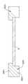
기타 실시예들에서 및 도 15에 도시된 바와 같이, 구조 홀더(1320)는 도 13 및 도 14에 도시된 것과 비슷하거나 동일한 후방 판(1346) 및 돌기(1347)를 포함한다. 기판 홀더(1320)는 전방 판(1351) 및 구조(9)의 전면에서 그루브(1357)에 수납되도록 그 크기가 정해지고 형태가 만들어지는 전방 돌기(1355)를 포함한다.In other embodiments and as shown in FIG. 15, the
도 16-18을 참조하면, 이 실시예의 구조 홀더(1420)는 구조(9)를 지지하기 위한 평탄 후방 판(1461) 및 구조를 수납하고 압착하기 위한 원형 개구부를 가진 전반적 원형 압착부(1460)를 포함한다. 평탄 판은 도 16-18에서와 같이 구조의 중심을 향하여 부분적으로만 연장될 수 있거나 또는 구조(9)의 아래에서 연속적으로 연장될 수 있다. 압착부(1460)는 연속적으로 구조를 둘러쌀 수 있거나, 또는 도 18에 도시된 바와 같이 구조(9)를 수납하기 위한 개구부를 형성하는 복수의 원호 형태(arc-shaped) 세그먼트(1563)를 포함할 수 있다. 압착부(1460) 및/또는 세그먼트들(1563)은 구조를 압착하기 위해 구조(9)에 상대적으로 내측으로 이동 가능할 수 있다.16-18, the
도 19를 참조하면, 구조 홀더(1620)는 전반적 평탄 후방 판(1681) 및 플랜지(1683)를 포함한다. 구조(9)는 구조의 주변 에지 부근에서 구조의 후면에 부착되는 링(1680)을 포함한다. 플랜지(1683)는 링(1680)과 맞물리도록 적응된다. 지지부(1681) 및 플랜지(1683)는 구조를 압착하기 위해 구조에 상대적으로 이동 가능하다.Referring to FIG. 19, the
몇몇 실시예들에서, 앞서 기술된 장치에 의해 가해지는 변형력은 (예를 들어, 주변 또는 메인 챔버들에서 압력을 감소시키거나 증가시킴으로써) 구조에 걸리는 차압을 감소시킴으로써 그런 것처럼 또는 기판을 파지하는 장치로 가해지는 변형력을 감소시킴으로써 그런 것처럼 순환된다(cycled). 그와 같은 순환은 구조에 형성되는 어떠한 탄성 응력도 해소할 수 있다.In some embodiments, the deformation force exerted by the apparatus described above is such that by reducing the differential pressure applied to the structure (e.g., by reducing or increasing the pressure in the surrounding or main chambers) or by the apparatus holding the substrate. It is cycled as it is by reducing the strain applied to it. Such circulation can relieve any elastic stresses that form in the structure.
본 명세서에 사용된 바로는, "약", "실질적으로", "본질적으로", 및 "대략적으로"라는 용어들은, 치수들, 농도들, 온도들 또는 기타 물리적이거나 화학적 속성들 또는 특성들의 범위들과 연계하여 사용될 때, 예를 들어 반올림, 측정 방법론 또는 기타 통계적 변동에 기인하는 변동들을 포함하여 속성들 또는 특성들의 범위들의 상한 및/또는 하한에 존재할 수 있는 변동들을 포함하기 위해 의도된 것이다.As used herein, the terms "about", "substantially", "essentially", and "approximately" refer to a range of dimensions, concentrations, temperatures or other physical or chemical properties or properties. When used in conjunction with, it is intended to include variations that may exist in the upper and/or lower limits of ranges of attributes or properties, including variations due to, for example, rounding, measurement methodology or other statistical variation.
본 개시의 요소들 또는 이것의 바람직한 실시예(들)를 도입할 때, 단수 표현들 및 "상기"는 하나 이상의 요소들이 존재한다는 것을 의미하도록 의도된 것이다. 용어들 "포함하는", "구비하는" 및 "갖는"은 배타적이 아니며 또한 나열된 요소들 외에 추가적 요소들이 있을 수 있다는 것을 의미하도록 의도된 것이다. When introducing elements of the present disclosure or preferred embodiment(s) thereof, the singular expressions and “above” are intended to mean that one or more elements are present. The terms "comprising", "having" and "having" are not exclusive and are intended to mean that there may be additional elements in addition to the listed elements.
본 개시의 범위에서 벗어나지 않으면서 상기 장치 및 방법에서 다양한 변화들이 이루어질 수 있기 때문에, 상기 상세한 설명에 포함되고 첨부된 도면들에 도시된 모든 사항들은 예시적인 것으로 해석해야 하고 제한적인 의미로 해석해서는 안 된다. Since various changes can be made in the apparatus and method without departing from the scope of the present disclosure, all matters included in the detailed description and shown in the accompanying drawings should be interpreted as illustrative and not in a limiting sense. do.
Claims (35)
Translated fromKorean전위 소스 층을 상기 기판에 형성하는 단계; 및
전위들을 발생하고 또한 상기 전위 소스 층으로부터 상기 표면 층을 향하여 상기 전위들을 미끄러지게(glide) 하기 위해 상기 기판을 방사상으로 압착하는 단계
를 포함하는 변형 릴랙스 공정.A process for relaxing deformation in a heterogeneous structure including a substrate, a surface layer disposed on the substrate, and an interface between the substrate and the surface layer, wherein the substrate is a central axis, a rear surface generally perpendicular to the central axis, and Including a diameter extending across the substrate through the central axis -:
Forming a potential source layer on the substrate; And
Radially compressing the substrate to generate dislocations and also to glide the dislocations from the dislocation source layer toward the surface layer.
Deformation relaxation process comprising a.
반도체 물질을 포함하는 잉곳(ingot)으로부터 상기 기판을 슬라이싱하거나;
상기 기판의 상기 후면을 래핑(lapping)하거나;
상기 기판의 후면을 모래 분사(sand blasting)하거나;
상기 기판의 후면을 통하여 이온들을 상기 기판에 주입함으로써 형성되는 변형 릴랙스 공정.The method of claim 1, wherein the potential source layer,
Slicing the substrate from an ingot containing a semiconductor material;
Wrapping the rear surface of the substrate;
Sand blasting the rear surface of the substrate;
A strain relaxation process formed by implanting ions into the substrate through the rear surface of the substrate.
반도체 기판의 전면 상에 표면 층을 피착하고, 그에 의해 상기 표면 층과 상기 기판 간의 변형을 생성하는 단계; 및
제1항의 공정에 의해 상기 표면 층 및 상기 기판에서 상기 변형을 릴랙스하는 단계
를 포함하는 릴랙스된 이종구조 제조 공정.As a process for manufacturing a relaxed heterostructure:
Depositing a surface layer on the front surface of a semiconductor substrate, thereby creating a strain between the surface layer and the substrate; And
Relaxing the deformation in the surface layer and the substrate by the process of claim 1
Relaxed heterogeneous structure manufacturing process comprising a.
상기 최상부 판, 상기 후방 판 및 상기 구조의 원주 둘레 간에 주위 챔버(peripheral chamber)를 형성하는 단계; 및
방사상으로 상기 구조를 압착하기 위해 상기 주위 챔버에서의 압력을 변화시키는 단계
를 포함하는 압착 방법.A method for radially compressing a semiconductor structure in a device, the structure having a front surface, a rear surface and a circumference of a circumference, the device comprising a top plate and a rear plate for contacting the structure adjacent to the circumference of the structure. A structural holder, wherein the top plate is adapted to contact the front surface of the structure and the rear plate is adapted to contact the rear surface of the structure -:
Forming a peripheral chamber between the top plate, the rear plate and the circumference of the structure; And
Varying the pressure in the surrounding chamber to radially compress the structure.
Compression method comprising a.
상기 후방 판 상에 상기 반도체 구조를 위치시키고; 및
상기 구조 상으로 상기 최상부 판을 낮춤으로써 형성되는
압착 방법.The method of claim 13, wherein the surrounding chamber is:
Positioning the semiconductor structure on the back plate; And
Formed by lowering the top plate in the structure
Crimping method.
상기 최상부 판과 상기 구조의 전면 사이에 중앙 챔버를 형성하는 단계; 및
상기 중앙 챔버에서의 압력을 감소시킴으로써 상기 중앙 챔버에서의 압력을 변화시키는 단계
를 포함하는 압착 방법.The method of claim 13, wherein the top plate comprises a recess defined by an annular wall, the method comprising:
Forming a central chamber between the top plate and the front surface of the structure; And
Changing the pressure in the central chamber by reducing the pressure in the central chamber.
Compression method comprising a.
상기 기판은 중앙 축, 상기 중앙 축에 전반적으로 수직인 전면 및 후면, 상기 전면으로부터 상기 후면으로 연장하는 주변 에지 및 상기 주변 에지에 인접하는 상기 후면 내의 원주 그루브를 가지며, 상기 장치는,
기판 홀더를 포함하고,
상기 기판 홀더는 상기 기판의 상기 후면 내의 상기 그루브에 수납되도록 크기가 정해지는 환형 돌기를 갖는 전반적 평탄 후방 판을 포함하고, 상기 돌기는 상기 기판 상에 변형력을 가하도록 이동 가능한 장치.As a device for applying a deformation force to an overall circular semiconductor substrate,
The substrate has a central axis, a front surface and a rear surface generally perpendicular to the central axis, a peripheral edge extending from the front surface to the rear surface, and a circumferential groove in the rear surface adjacent the peripheral edge, the device comprising:
Including a substrate holder,
The substrate holder includes an overall flat rear plate having an annular protrusion sized to be received in the groove in the rear surface of the substrate, the protrusion being movable to apply a deforming force on the substrate.
상기 기판은 중앙 축, 상기 중앙 축에 전반적으로 수직인 전면 및 후면, 상기 전면으로부터 상기 후면으로 연장하는 주변 에지 및 상기 주변 에지에 인접하게 상기 후면에 본딩되는 링을 가지며, 상기 장치는,
기판 홀더를 포함하고,
상기 기판 홀더는 상기 기판의 상기 후면 상에서 상기 링과 맞물리도록 적응되는 플랜지를 갖는 전반적 평탄 후방 지지부를 포함하고, 상기 지지부는 상기 기판 상에 변형력을 가하도록 이동 가능한 장치.As a device for applying a deformation force to an overall circular semiconductor substrate,
The substrate has a central axis, a front surface and a rear surface generally perpendicular to the central axis, a peripheral edge extending from the front surface to the rear surface, and a ring bonded to the rear surface adjacent the peripheral edge, the device comprising:
Including a substrate holder,
The substrate holder includes a generally flat rear support having a flange adapted to engage the ring on the rear surface of the substrate, the support being movable to apply a deforming force on the substrate.
상기 기판은 중앙 축, 상기 중앙 축에 전반적으로 수직인 전면 및 후면, 및 상기 전면으로부터 상기 후면으로 연장하는 주변 에지를 가지며, 상기 장치는,
챔버 내에 탑재된 기판 홀더를 포함하고,
상기 홀더는,
전반적 평탄 후방 판; 및
상기 기판을 수납하고 압착하기 위한 압착부
를 포함하고, 상기 압착부는 상기 기판을 그의 주변 에지에서 그의 중앙 축을 향해 방사상으로 안쪽으로 압착하도록 적응되는 장치.As a device for applying a deformation force to a semiconductor substrate,
The substrate has a central axis, a front surface and a rear surface generally perpendicular to the central axis, and a peripheral edge extending from the front surface to the rear surface, the device comprising:
Including a substrate holder mounted in the chamber,
The holder,
Overall flat rear plate; And
Crimping portion for accommodating and compressing the substrate
Wherein the crimp portion is adapted to compress the substrate radially inwardly toward its central axis at its peripheral edge.
중앙 축에 내측으로 포인팅하는 삼각형 모양 세그먼트들 - 상기 세그먼트들은 상기 구조에 변형력을 가하기 위해 상기 중앙 축으로부터 이동하도록 구성됨 -; 및
상기 세그먼트와 구조 사이에 진공을 형성하기 위해 각각의 세그먼트 내에 형성된 유체 통로들
을 포함하는 장치.A device for radially applying strain to a semiconductor structure having a front, a rear, a circumferential edge and a central axis,
Triangular-shaped segments pointing inwardly to a central axis, the segments configured to move from the central axis to apply a deforming force to the structure; And
Fluid passageways formed within each segment to create a vacuum between the segment and the structure
Device comprising a.
Applications Claiming Priority (9)
| Application Number | Priority Date | Filing Date | Title |
|---|---|---|---|
| US201261747613P | 2012-12-31 | 2012-12-31 | |
| US61/747,613 | 2012-12-31 | ||
| US201361788744P | 2013-03-15 | 2013-03-15 | |
| US201361790445P | 2013-03-15 | 2013-03-15 | |
| US201361793999P | 2013-03-15 | 2013-03-15 | |
| US61/788,744 | 2013-03-15 | ||
| US61/793,999 | 2013-03-15 | ||
| US61/790,445 | 2013-03-15 | ||
| PCT/US2013/078295WO2014106177A1 (en) | 2012-12-31 | 2013-12-30 | Processes and apparatus for preparing heterostructures with reduced strain by radial compression |
Publications (2)
| Publication Number | Publication Date |
|---|---|
| KR20150103698A KR20150103698A (en) | 2015-09-11 |
| KR102224422B1true KR102224422B1 (en) | 2021-03-08 |
Family
ID=49958756
Family Applications (2)
| Application Number | Title | Priority Date | Filing Date |
|---|---|---|---|
| KR1020157020443AActiveKR102203560B1 (en) | 2012-12-31 | 2013-12-30 | Processes and apparatus for preparing heterostructures with reduced strain by radial distention |
| KR1020157020444AActiveKR102224422B1 (en) | 2012-12-31 | 2013-12-30 | Processes and apparatus for preparing heterostructures with reduced strain by radial compression |
Family Applications Before (1)
| Application Number | Title | Priority Date | Filing Date |
|---|---|---|---|
| KR1020157020443AActiveKR102203560B1 (en) | 2012-12-31 | 2013-12-30 | Processes and apparatus for preparing heterostructures with reduced strain by radial distention |
Country Status (7)
| Country | Link |
|---|---|
| US (7) | US9583363B2 (en) |
| EP (6) | EP3188224B1 (en) |
| JP (10) | JP6314153B2 (en) |
| KR (2) | KR102203560B1 (en) |
| CN (5) | CN107968067B (en) |
| TW (4) | TWI673865B (en) |
| WO (3) | WO2014106177A1 (en) |
Families Citing this family (266)
| Publication number | Priority date | Publication date | Assignee | Title |
|---|---|---|---|---|
| US20130023129A1 (en) | 2011-07-20 | 2013-01-24 | Asm America, Inc. | Pressure transmitter for a semiconductor processing environment |
| US10714315B2 (en) | 2012-10-12 | 2020-07-14 | Asm Ip Holdings B.V. | Semiconductor reaction chamber showerhead |
| US9583363B2 (en)* | 2012-12-31 | 2017-02-28 | Sunedison Semiconductor Limited (Uen201334164H) | Processes and apparatus for preparing heterostructures with reduced strain by radial distension |
| US20160376700A1 (en) | 2013-02-01 | 2016-12-29 | Asm Ip Holding B.V. | System for treatment of deposition reactor |
| WO2014191624A1 (en)* | 2013-05-29 | 2014-12-04 | Beneq Oy | Substrate holder and arrangement for holding substrates |
| WO2014191621A1 (en)* | 2013-05-29 | 2014-12-04 | Beneq Oy | Substrate carrier and arrangement for supporting substrates |
| US10941490B2 (en) | 2014-10-07 | 2021-03-09 | Asm Ip Holding B.V. | Multiple temperature range susceptor, assembly, reactor and system including the susceptor, and methods of using the same |
| US10276355B2 (en) | 2015-03-12 | 2019-04-30 | Asm Ip Holding B.V. | Multi-zone reactor, system including the reactor, and method of using the same |
| US10458018B2 (en) | 2015-06-26 | 2019-10-29 | Asm Ip Holding B.V. | Structures including metal carbide material, devices including the structures, and methods of forming same |
| US10211308B2 (en) | 2015-10-21 | 2019-02-19 | Asm Ip Holding B.V. | NbMC layers |
| DE102015223807A1 (en)* | 2015-12-01 | 2017-06-01 | Siltronic Ag | Process for producing a semiconductor wafer with epitaxial layer in a deposition chamber, apparatus for producing an epitaxial-layer semiconductor wafer and semiconductor wafer with epitaxial layer |
| US11139308B2 (en) | 2015-12-29 | 2021-10-05 | Asm Ip Holding B.V. | Atomic layer deposition of III-V compounds to form V-NAND devices |
| US10529554B2 (en) | 2016-02-19 | 2020-01-07 | Asm Ip Holding B.V. | Method for forming silicon nitride film selectively on sidewalls or flat surfaces of trenches |
| US10343920B2 (en) | 2016-03-18 | 2019-07-09 | Asm Ip Holding B.V. | Aligned carbon nanotubes |
| US11453943B2 (en) | 2016-05-25 | 2022-09-27 | Asm Ip Holding B.V. | Method for forming carbon-containing silicon/metal oxide or nitride film by ALD using silicon precursor and hydrocarbon precursor |
| US10612137B2 (en) | 2016-07-08 | 2020-04-07 | Asm Ip Holdings B.V. | Organic reactants for atomic layer deposition |
| US9859151B1 (en) | 2016-07-08 | 2018-01-02 | Asm Ip Holding B.V. | Selective film deposition method to form air gaps |
| CN107623028B (en)* | 2016-07-13 | 2021-02-19 | 环球晶圆股份有限公司 | Semiconductor substrate and processing method thereof |
| US9887082B1 (en) | 2016-07-28 | 2018-02-06 | Asm Ip Holding B.V. | Method and apparatus for filling a gap |
| US9812320B1 (en) | 2016-07-28 | 2017-11-07 | Asm Ip Holding B.V. | Method and apparatus for filling a gap |
| CN109564868B (en)* | 2016-08-25 | 2023-04-04 | 日本瑞翁株式会社 | Plasma etching method |
| US11532757B2 (en) | 2016-10-27 | 2022-12-20 | Asm Ip Holding B.V. | Deposition of charge trapping layers |
| US10714350B2 (en) | 2016-11-01 | 2020-07-14 | ASM IP Holdings, B.V. | Methods for forming a transition metal niobium nitride film on a substrate by atomic layer deposition and related semiconductor device structures |
| KR102546317B1 (en) | 2016-11-15 | 2023-06-21 | 에이에스엠 아이피 홀딩 비.브이. | Gas supply unit and substrate processing apparatus including the same |
| KR102762543B1 (en) | 2016-12-14 | 2025-02-05 | 에이에스엠 아이피 홀딩 비.브이. | Substrate processing apparatus |
| US11581186B2 (en) | 2016-12-15 | 2023-02-14 | Asm Ip Holding B.V. | Sequential infiltration synthesis apparatus |
| US11447861B2 (en) | 2016-12-15 | 2022-09-20 | Asm Ip Holding B.V. | Sequential infiltration synthesis apparatus and a method of forming a patterned structure |
| US10269558B2 (en) | 2016-12-22 | 2019-04-23 | Asm Ip Holding B.V. | Method of forming a structure on a substrate |
| US10068787B2 (en)* | 2016-12-30 | 2018-09-04 | Sunpower Corporation | Bowing semiconductor wafers |
| US11390950B2 (en) | 2017-01-10 | 2022-07-19 | Asm Ip Holding B.V. | Reactor system and method to reduce residue buildup during a film deposition process |
| US10468261B2 (en) | 2017-02-15 | 2019-11-05 | Asm Ip Holding B.V. | Methods for forming a metallic film on a substrate by cyclical deposition and related semiconductor device structures |
| US10770286B2 (en) | 2017-05-08 | 2020-09-08 | Asm Ip Holdings B.V. | Methods for selectively forming a silicon nitride film on a substrate and related semiconductor device structures |
| KR102015336B1 (en)* | 2017-06-12 | 2019-08-28 | 삼성전자주식회사 | Method of reducing warpage of semiconductor package substrate and warpage reducer device |
| US12040200B2 (en) | 2017-06-20 | 2024-07-16 | Asm Ip Holding B.V. | Semiconductor processing apparatus and methods for calibrating a semiconductor processing apparatus |
| US11306395B2 (en) | 2017-06-28 | 2022-04-19 | Asm Ip Holding B.V. | Methods for depositing a transition metal nitride film on a substrate by atomic layer deposition and related deposition apparatus |
| KR20190009245A (en) | 2017-07-18 | 2019-01-28 | 에이에스엠 아이피 홀딩 비.브이. | Methods for forming a semiconductor device structure and related semiconductor device structures |
| US11374112B2 (en) | 2017-07-19 | 2022-06-28 | Asm Ip Holding B.V. | Method for depositing a group IV semiconductor and related semiconductor device structures |
| US10590535B2 (en) | 2017-07-26 | 2020-03-17 | Asm Ip Holdings B.V. | Chemical treatment, deposition and/or infiltration apparatus and method for using the same |
| TWI815813B (en) | 2017-08-04 | 2023-09-21 | 荷蘭商Asm智慧財產控股公司 | Showerhead assembly for distributing a gas within a reaction chamber |
| US10692741B2 (en) | 2017-08-08 | 2020-06-23 | Asm Ip Holdings B.V. | Radiation shield |
| US10770336B2 (en) | 2017-08-08 | 2020-09-08 | Asm Ip Holding B.V. | Substrate lift mechanism and reactor including same |
| US11769682B2 (en) | 2017-08-09 | 2023-09-26 | Asm Ip Holding B.V. | Storage apparatus for storing cassettes for substrates and processing apparatus equipped therewith |
| US11830730B2 (en) | 2017-08-29 | 2023-11-28 | Asm Ip Holding B.V. | Layer forming method and apparatus |
| US11295980B2 (en) | 2017-08-30 | 2022-04-05 | Asm Ip Holding B.V. | Methods for depositing a molybdenum metal film over a dielectric surface of a substrate by a cyclical deposition process and related semiconductor device structures |
| US10658205B2 (en) | 2017-09-28 | 2020-05-19 | Asm Ip Holdings B.V. | Chemical dispensing apparatus and methods for dispensing a chemical to a reaction chamber |
| US10403504B2 (en) | 2017-10-05 | 2019-09-03 | Asm Ip Holding B.V. | Method for selectively depositing a metallic film on a substrate |
| US10923344B2 (en) | 2017-10-30 | 2021-02-16 | Asm Ip Holding B.V. | Methods for forming a semiconductor structure and related semiconductor structures |
| WO2019103613A1 (en) | 2017-11-27 | 2019-05-31 | Asm Ip Holding B.V. | A storage device for storing wafer cassettes for use with a batch furnace |
| CN111344522B (en) | 2017-11-27 | 2022-04-12 | 阿斯莫Ip控股公司 | Including clean mini-environment device |
| US10872771B2 (en) | 2018-01-16 | 2020-12-22 | Asm Ip Holding B. V. | Method for depositing a material film on a substrate within a reaction chamber by a cyclical deposition process and related device structures |
| TWI799494B (en) | 2018-01-19 | 2023-04-21 | 荷蘭商Asm 智慧財產控股公司 | Deposition method |
| KR102695659B1 (en) | 2018-01-19 | 2024-08-14 | 에이에스엠 아이피 홀딩 비.브이. | Method for depositing a gap filling layer by plasma assisted deposition |
| US11081345B2 (en) | 2018-02-06 | 2021-08-03 | Asm Ip Holding B.V. | Method of post-deposition treatment for silicon oxide film |
| US10896820B2 (en) | 2018-02-14 | 2021-01-19 | Asm Ip Holding B.V. | Method for depositing a ruthenium-containing film on a substrate by a cyclical deposition process |
| WO2019158960A1 (en) | 2018-02-14 | 2019-08-22 | Asm Ip Holding B.V. | A method for depositing a ruthenium-containing film on a substrate by a cyclical deposition process |
| US10731249B2 (en) | 2018-02-15 | 2020-08-04 | Asm Ip Holding B.V. | Method of forming a transition metal containing film on a substrate by a cyclical deposition process, a method for supplying a transition metal halide compound to a reaction chamber, and related vapor deposition apparatus |
| KR102636427B1 (en) | 2018-02-20 | 2024-02-13 | 에이에스엠 아이피 홀딩 비.브이. | Substrate processing method and apparatus |
| US10975470B2 (en) | 2018-02-23 | 2021-04-13 | Asm Ip Holding B.V. | Apparatus for detecting or monitoring for a chemical precursor in a high temperature environment |
| US11473195B2 (en) | 2018-03-01 | 2022-10-18 | Asm Ip Holding B.V. | Semiconductor processing apparatus and a method for processing a substrate |
| US11629406B2 (en) | 2018-03-09 | 2023-04-18 | Asm Ip Holding B.V. | Semiconductor processing apparatus comprising one or more pyrometers for measuring a temperature of a substrate during transfer of the substrate |
| KR102646467B1 (en) | 2018-03-27 | 2024-03-11 | 에이에스엠 아이피 홀딩 비.브이. | Method of forming an electrode on a substrate and a semiconductor device structure including an electrode |
| US11230766B2 (en) | 2018-03-29 | 2022-01-25 | Asm Ip Holding B.V. | Substrate processing apparatus and method |
| KR102600229B1 (en) | 2018-04-09 | 2023-11-10 | 에이에스엠 아이피 홀딩 비.브이. | Substrate supporting device, substrate processing apparatus including the same and substrate processing method |
| US12025484B2 (en) | 2018-05-08 | 2024-07-02 | Asm Ip Holding B.V. | Thin film forming method |
| TWI811348B (en) | 2018-05-08 | 2023-08-11 | 荷蘭商Asm 智慧財產控股公司 | Methods for depositing an oxide film on a substrate by a cyclical deposition process and related device structures |
| US12272527B2 (en) | 2018-05-09 | 2025-04-08 | Asm Ip Holding B.V. | Apparatus for use with hydrogen radicals and method of using same |
| KR102596988B1 (en) | 2018-05-28 | 2023-10-31 | 에이에스엠 아이피 홀딩 비.브이. | Method of processing a substrate and a device manufactured by the same |
| US11201079B2 (en)* | 2018-05-30 | 2021-12-14 | Taiwan Semiconductor Manufacturing Company, Ltd. | Wafer chuck |
| US11718913B2 (en) | 2018-06-04 | 2023-08-08 | Asm Ip Holding B.V. | Gas distribution system and reactor system including same |
| TWI840362B (en) | 2018-06-04 | 2024-05-01 | 荷蘭商Asm Ip私人控股有限公司 | Wafer handling chamber with moisture reduction |
| US11286562B2 (en) | 2018-06-08 | 2022-03-29 | Asm Ip Holding B.V. | Gas-phase chemical reactor and method of using same |
| KR102568797B1 (en) | 2018-06-21 | 2023-08-21 | 에이에스엠 아이피 홀딩 비.브이. | Substrate processing system |
| US10797133B2 (en) | 2018-06-21 | 2020-10-06 | Asm Ip Holding B.V. | Method for depositing a phosphorus doped silicon arsenide film and related semiconductor device structures |
| KR102854019B1 (en) | 2018-06-27 | 2025-09-02 | 에이에스엠 아이피 홀딩 비.브이. | Periodic deposition method for forming a metal-containing material and films and structures comprising the metal-containing material |
| TWI873894B (en) | 2018-06-27 | 2025-02-21 | 荷蘭商Asm Ip私人控股有限公司 | Cyclic deposition methods for forming metal-containing material and films and structures including the metal-containing material |
| US10612136B2 (en) | 2018-06-29 | 2020-04-07 | ASM IP Holding, B.V. | Temperature-controlled flange and reactor system including same |
| US10755922B2 (en) | 2018-07-03 | 2020-08-25 | Asm Ip Holding B.V. | Method for depositing silicon-free carbon-containing film as gap-fill layer by pulse plasma-assisted deposition |
| US10388513B1 (en) | 2018-07-03 | 2019-08-20 | Asm Ip Holding B.V. | Method for depositing silicon-free carbon-containing film as gap-fill layer by pulse plasma-assisted deposition |
| US11430674B2 (en) | 2018-08-22 | 2022-08-30 | Asm Ip Holding B.V. | Sensor array, apparatus for dispensing a vapor phase reactant to a reaction chamber and related methods |
| US11024523B2 (en) | 2018-09-11 | 2021-06-01 | Asm Ip Holding B.V. | Substrate processing apparatus and method |
| KR102707956B1 (en) | 2018-09-11 | 2024-09-19 | 에이에스엠 아이피 홀딩 비.브이. | Method for deposition of a thin film |
| CN110970344B (en) | 2018-10-01 | 2024-10-25 | Asmip控股有限公司 | Substrate holding apparatus, system comprising the same and method of using the same |
| US11232963B2 (en) | 2018-10-03 | 2022-01-25 | Asm Ip Holding B.V. | Substrate processing apparatus and method |
| KR102592699B1 (en) | 2018-10-08 | 2023-10-23 | 에이에스엠 아이피 홀딩 비.브이. | Substrate support unit and apparatuses for depositing thin film and processing the substrate including the same |
| KR102546322B1 (en) | 2018-10-19 | 2023-06-21 | 에이에스엠 아이피 홀딩 비.브이. | Substrate processing apparatus and substrate processing method |
| KR102605121B1 (en) | 2018-10-19 | 2023-11-23 | 에이에스엠 아이피 홀딩 비.브이. | Substrate processing apparatus and substrate processing method |
| US12378665B2 (en) | 2018-10-26 | 2025-08-05 | Asm Ip Holding B.V. | High temperature coatings for a preclean and etch apparatus and related methods |
| US11087997B2 (en) | 2018-10-31 | 2021-08-10 | Asm Ip Holding B.V. | Substrate processing apparatus for processing substrates |
| KR102748291B1 (en) | 2018-11-02 | 2024-12-31 | 에이에스엠 아이피 홀딩 비.브이. | Substrate support unit and substrate processing apparatus including the same |
| US11572620B2 (en) | 2018-11-06 | 2023-02-07 | Asm Ip Holding B.V. | Methods for selectively depositing an amorphous silicon film on a substrate |
| US10818758B2 (en) | 2018-11-16 | 2020-10-27 | Asm Ip Holding B.V. | Methods for forming a metal silicate film on a substrate in a reaction chamber and related semiconductor device structures |
| US12040199B2 (en) | 2018-11-28 | 2024-07-16 | Asm Ip Holding B.V. | Substrate processing apparatus for processing substrates |
| US11217444B2 (en) | 2018-11-30 | 2022-01-04 | Asm Ip Holding B.V. | Method for forming an ultraviolet radiation responsive metal oxide-containing film |
| KR102636428B1 (en) | 2018-12-04 | 2024-02-13 | 에이에스엠 아이피 홀딩 비.브이. | A method for cleaning a substrate processing apparatus |
| US11158513B2 (en) | 2018-12-13 | 2021-10-26 | Asm Ip Holding B.V. | Methods for forming a rhenium-containing film on a substrate by a cyclical deposition process and related semiconductor device structures |
| TWI874340B (en) | 2018-12-14 | 2025-03-01 | 荷蘭商Asm Ip私人控股有限公司 | Method of forming device structure, structure formed by the method and system for performing the method |
| TWI866480B (en) | 2019-01-17 | 2024-12-11 | 荷蘭商Asm Ip 私人控股有限公司 | Methods of forming a transition metal containing film on a substrate by a cyclical deposition process |
| KR102727227B1 (en) | 2019-01-22 | 2024-11-07 | 에이에스엠 아이피 홀딩 비.브이. | Semiconductor processing device |
| TWI838458B (en)* | 2019-02-20 | 2024-04-11 | 荷蘭商Asm Ip私人控股有限公司 | Apparatus and methods for plug fill deposition in 3-d nand applications |
| TWI845607B (en) | 2019-02-20 | 2024-06-21 | 荷蘭商Asm Ip私人控股有限公司 | Cyclical deposition method and apparatus for filling a recess formed within a substrate surface |
| KR102626263B1 (en) | 2019-02-20 | 2024-01-16 | 에이에스엠 아이피 홀딩 비.브이. | Cyclical deposition method including treatment step and apparatus for same |
| TWI873122B (en) | 2019-02-20 | 2025-02-21 | 荷蘭商Asm Ip私人控股有限公司 | Method of filling a recess formed within a surface of a substrate, semiconductor structure formed according to the method, and semiconductor processing apparatus |
| TWI842826B (en) | 2019-02-22 | 2024-05-21 | 荷蘭商Asm Ip私人控股有限公司 | Substrate processing apparatus and method for processing substrate |
| KR102858005B1 (en) | 2019-03-08 | 2025-09-09 | 에이에스엠 아이피 홀딩 비.브이. | Method for Selective Deposition of Silicon Nitride Layer and Structure Including Selectively-Deposited Silicon Nitride Layer |
| US11742198B2 (en) | 2019-03-08 | 2023-08-29 | Asm Ip Holding B.V. | Structure including SiOCN layer and method of forming same |
| KR102673983B1 (en)* | 2019-03-15 | 2024-06-12 | 주식회사 케이씨텍 | Apparatus for Treating Substrate |
| JP7279465B2 (en)* | 2019-03-28 | 2023-05-23 | 住友金属鉱山株式会社 | SUPPORTING SUBSTRATE, SUPPORTING SUBSTRATE HOLDING METHOD, AND FILM-FORMING METHOD |
| JP2020167398A (en) | 2019-03-28 | 2020-10-08 | エーエスエム・アイピー・ホールディング・ベー・フェー | Door openers and substrate processing equipment provided with door openers |
| KR102809999B1 (en) | 2019-04-01 | 2025-05-19 | 에이에스엠 아이피 홀딩 비.브이. | Method of manufacturing semiconductor device |
| KR20200123380A (en) | 2019-04-19 | 2020-10-29 | 에이에스엠 아이피 홀딩 비.브이. | Layer forming method and apparatus |
| KR20200125453A (en) | 2019-04-24 | 2020-11-04 | 에이에스엠 아이피 홀딩 비.브이. | Gas-phase reactor system and method of using same |
| KR20200130121A (en) | 2019-05-07 | 2020-11-18 | 에이에스엠 아이피 홀딩 비.브이. | Chemical source vessel with dip tube |
| US11289326B2 (en) | 2019-05-07 | 2022-03-29 | Asm Ip Holding B.V. | Method for reforming amorphous carbon polymer film |
| KR20200130652A (en) | 2019-05-10 | 2020-11-19 | 에이에스엠 아이피 홀딩 비.브이. | Method of depositing material onto a surface and structure formed according to the method |
| JP7612342B2 (en) | 2019-05-16 | 2025-01-14 | エーエスエム・アイピー・ホールディング・ベー・フェー | Wafer boat handling apparatus, vertical batch furnace and method |
| JP7598201B2 (en) | 2019-05-16 | 2024-12-11 | エーエスエム・アイピー・ホールディング・ベー・フェー | Wafer boat handling apparatus, vertical batch furnace and method |
| USD975665S1 (en) | 2019-05-17 | 2023-01-17 | Asm Ip Holding B.V. | Susceptor shaft |
| USD947913S1 (en) | 2019-05-17 | 2022-04-05 | Asm Ip Holding B.V. | Susceptor shaft |
| KR20200141002A (en) | 2019-06-06 | 2020-12-17 | 에이에스엠 아이피 홀딩 비.브이. | Method of using a gas-phase reactor system including analyzing exhausted gas |
| KR20200141931A (en) | 2019-06-10 | 2020-12-21 | 에이에스엠 아이피 홀딩 비.브이. | Method for cleaning quartz epitaxial chambers |
| KR20200143254A (en) | 2019-06-11 | 2020-12-23 | 에이에스엠 아이피 홀딩 비.브이. | Method of forming an electronic structure using an reforming gas, system for performing the method, and structure formed using the method |
| USD944946S1 (en) | 2019-06-14 | 2022-03-01 | Asm Ip Holding B.V. | Shower plate |
| KR20210005515A (en) | 2019-07-03 | 2021-01-14 | 에이에스엠 아이피 홀딩 비.브이. | Temperature control assembly for substrate processing apparatus and method of using same |
| JP7499079B2 (en) | 2019-07-09 | 2024-06-13 | エーエスエム・アイピー・ホールディング・ベー・フェー | Plasma device using coaxial waveguide and substrate processing method |
| CN112216646A (en) | 2019-07-10 | 2021-01-12 | Asm Ip私人控股有限公司 | Substrate supporting assembly and substrate processing device comprising same |
| KR20210010307A (en) | 2019-07-16 | 2021-01-27 | 에이에스엠 아이피 홀딩 비.브이. | Substrate processing apparatus |
| KR102860110B1 (en) | 2019-07-17 | 2025-09-16 | 에이에스엠 아이피 홀딩 비.브이. | Methods of forming silicon germanium structures |
| KR20210010816A (en) | 2019-07-17 | 2021-01-28 | 에이에스엠 아이피 홀딩 비.브이. | Radical assist ignition plasma system and method |
| US11643724B2 (en) | 2019-07-18 | 2023-05-09 | Asm Ip Holding B.V. | Method of forming structures using a neutral beam |
| TWI839544B (en) | 2019-07-19 | 2024-04-21 | 荷蘭商Asm Ip私人控股有限公司 | Method of forming topology-controlled amorphous carbon polymer film |
| KR20210010817A (en) | 2019-07-19 | 2021-01-28 | 에이에스엠 아이피 홀딩 비.브이. | Method of Forming Topology-Controlled Amorphous Carbon Polymer Film |
| TWI851767B (en) | 2019-07-29 | 2024-08-11 | 荷蘭商Asm Ip私人控股有限公司 | Methods for selective deposition utilizing n-type dopants and/or alternative dopants to achieve high dopant incorporation |
| CN112309900A (en) | 2019-07-30 | 2021-02-02 | Asm Ip私人控股有限公司 | Substrate processing apparatus |
| CN112309899A (en) | 2019-07-30 | 2021-02-02 | Asm Ip私人控股有限公司 | Substrate processing apparatus |
| US12169361B2 (en) | 2019-07-30 | 2024-12-17 | Asm Ip Holding B.V. | Substrate processing apparatus and method |
| US11587815B2 (en) | 2019-07-31 | 2023-02-21 | Asm Ip Holding B.V. | Vertical batch furnace assembly |
| US11227782B2 (en) | 2019-07-31 | 2022-01-18 | Asm Ip Holding B.V. | Vertical batch furnace assembly |
| US11587814B2 (en) | 2019-07-31 | 2023-02-21 | Asm Ip Holding B.V. | Vertical batch furnace assembly |
| CN112323048B (en) | 2019-08-05 | 2024-02-09 | Asm Ip私人控股有限公司 | Liquid level sensor for chemical source container |
| CN112342526A (en) | 2019-08-09 | 2021-02-09 | Asm Ip私人控股有限公司 | Heater assembly including cooling device and method of using same |
| USD965524S1 (en) | 2019-08-19 | 2022-10-04 | Asm Ip Holding B.V. | Susceptor support |
| USD965044S1 (en) | 2019-08-19 | 2022-09-27 | Asm Ip Holding B.V. | Susceptor shaft |
| JP2021031769A (en) | 2019-08-21 | 2021-03-01 | エーエスエム アイピー ホールディング ビー.ブイ. | Production apparatus of mixed gas of film deposition raw material and film deposition apparatus |
| USD979506S1 (en) | 2019-08-22 | 2023-02-28 | Asm Ip Holding B.V. | Insulator |
| KR20210024423A (en) | 2019-08-22 | 2021-03-05 | 에이에스엠 아이피 홀딩 비.브이. | Method for forming a structure with a hole |
| USD949319S1 (en) | 2019-08-22 | 2022-04-19 | Asm Ip Holding B.V. | Exhaust duct |
| USD940837S1 (en) | 2019-08-22 | 2022-01-11 | Asm Ip Holding B.V. | Electrode |
| KR20210024420A (en) | 2019-08-23 | 2021-03-05 | 에이에스엠 아이피 홀딩 비.브이. | Method for depositing silicon oxide film having improved quality by peald using bis(diethylamino)silane |
| US11286558B2 (en) | 2019-08-23 | 2022-03-29 | Asm Ip Holding B.V. | Methods for depositing a molybdenum nitride film on a surface of a substrate by a cyclical deposition process and related semiconductor device structures including a molybdenum nitride film |
| KR102806450B1 (en) | 2019-09-04 | 2025-05-12 | 에이에스엠 아이피 홀딩 비.브이. | Methods for selective deposition using a sacrificial capping layer |
| KR102733104B1 (en) | 2019-09-05 | 2024-11-22 | 에이에스엠 아이피 홀딩 비.브이. | Substrate processing apparatus |
| US11562901B2 (en) | 2019-09-25 | 2023-01-24 | Asm Ip Holding B.V. | Substrate processing method |
| CN112593212B (en) | 2019-10-02 | 2023-12-22 | Asm Ip私人控股有限公司 | Method for forming topologically selective silicon oxide film by cyclic plasma enhanced deposition process |
| TWI846953B (en) | 2019-10-08 | 2024-07-01 | 荷蘭商Asm Ip私人控股有限公司 | Substrate processing device |
| KR20210042810A (en) | 2019-10-08 | 2021-04-20 | 에이에스엠 아이피 홀딩 비.브이. | Reactor system including a gas distribution assembly for use with activated species and method of using same |
| TW202128273A (en) | 2019-10-08 | 2021-08-01 | 荷蘭商Asm Ip私人控股有限公司 | Gas injection system, reactor system, and method of depositing material on surface of substratewithin reaction chamber |
| TWI846966B (en) | 2019-10-10 | 2024-07-01 | 荷蘭商Asm Ip私人控股有限公司 | Method of forming a photoresist underlayer and structure including same |
| US12009241B2 (en) | 2019-10-14 | 2024-06-11 | Asm Ip Holding B.V. | Vertical batch furnace assembly with detector to detect cassette |
| TWI834919B (en) | 2019-10-16 | 2024-03-11 | 荷蘭商Asm Ip私人控股有限公司 | Method of topology-selective film formation of silicon oxide |
| US11637014B2 (en) | 2019-10-17 | 2023-04-25 | Asm Ip Holding B.V. | Methods for selective deposition of doped semiconductor material |
| KR102845724B1 (en) | 2019-10-21 | 2025-08-13 | 에이에스엠 아이피 홀딩 비.브이. | Apparatus and methods for selectively etching films |
| US11328944B2 (en)* | 2019-10-23 | 2022-05-10 | Eugenus, Inc. | Systems and methods of placing substrates in semiconductor manufacturing equipment |
| KR20210050453A (en) | 2019-10-25 | 2021-05-07 | 에이에스엠 아이피 홀딩 비.브이. | Methods for filling a gap feature on a substrate surface and related semiconductor structures |
| US11646205B2 (en) | 2019-10-29 | 2023-05-09 | Asm Ip Holding B.V. | Methods of selectively forming n-type doped material on a surface, systems for selectively forming n-type doped material, and structures formed using same |
| KR20210054983A (en) | 2019-11-05 | 2021-05-14 | 에이에스엠 아이피 홀딩 비.브이. | Structures with doped semiconductor layers and methods and systems for forming same |
| US11501968B2 (en) | 2019-11-15 | 2022-11-15 | Asm Ip Holding B.V. | Method for providing a semiconductor device with silicon filled gaps |
| KR102861314B1 (en) | 2019-11-20 | 2025-09-17 | 에이에스엠 아이피 홀딩 비.브이. | Method of depositing carbon-containing material on a surface of a substrate, structure formed using the method, and system for forming the structure |
| US11450529B2 (en) | 2019-11-26 | 2022-09-20 | Asm Ip Holding B.V. | Methods for selectively forming a target film on a substrate comprising a first dielectric surface and a second metallic surface |
| CN112951697B (en) | 2019-11-26 | 2025-07-29 | Asmip私人控股有限公司 | Substrate processing apparatus |
| CN112885692B (en) | 2019-11-29 | 2025-08-15 | Asmip私人控股有限公司 | Substrate processing apparatus |
| CN120432376A (en) | 2019-11-29 | 2025-08-05 | Asm Ip私人控股有限公司 | Substrate processing apparatus |
| JP7527928B2 (en) | 2019-12-02 | 2024-08-05 | エーエスエム・アイピー・ホールディング・ベー・フェー | Substrate processing apparatus and substrate processing method |
| KR20210070898A (en) | 2019-12-04 | 2021-06-15 | 에이에스엠 아이피 홀딩 비.브이. | Substrate processing apparatus |
| KR20210078405A (en) | 2019-12-17 | 2021-06-28 | 에이에스엠 아이피 홀딩 비.브이. | Method of forming vanadium nitride layer and structure including the vanadium nitride layer |
| KR20210080214A (en) | 2019-12-19 | 2021-06-30 | 에이에스엠 아이피 홀딩 비.브이. | Methods for filling a gap feature on a substrate and related semiconductor structures |
| JP7730637B2 (en) | 2020-01-06 | 2025-08-28 | エーエスエム・アイピー・ホールディング・ベー・フェー | Gas delivery assembly, components thereof, and reactor system including same |
| JP7636892B2 (en) | 2020-01-06 | 2025-02-27 | エーエスエム・アイピー・ホールディング・ベー・フェー | Channeled Lift Pins |
| US11993847B2 (en) | 2020-01-08 | 2024-05-28 | Asm Ip Holding B.V. | Injector |
| KR20210093163A (en) | 2020-01-16 | 2021-07-27 | 에이에스엠 아이피 홀딩 비.브이. | Method of forming high aspect ratio features |
| US11791192B2 (en)* | 2020-01-19 | 2023-10-17 | Taiwan Semiconductor Manufacturing Company, Ltd. | Workpiece holder, wafer chuck, wafer holding method |
| KR102675856B1 (en) | 2020-01-20 | 2024-06-17 | 에이에스엠 아이피 홀딩 비.브이. | Method of forming thin film and method of modifying surface of thin film |
| TWI889744B (en) | 2020-01-29 | 2025-07-11 | 荷蘭商Asm Ip私人控股有限公司 | Contaminant trap system, and baffle plate stack |
| TW202513845A (en) | 2020-02-03 | 2025-04-01 | 荷蘭商Asm Ip私人控股有限公司 | Semiconductor structures and methods for forming the same |
| KR20210100010A (en) | 2020-02-04 | 2021-08-13 | 에이에스엠 아이피 홀딩 비.브이. | Method and apparatus for transmittance measurements of large articles |
| US11776846B2 (en) | 2020-02-07 | 2023-10-03 | Asm Ip Holding B.V. | Methods for depositing gap filling fluids and related systems and devices |
| KR20210103956A (en) | 2020-02-13 | 2021-08-24 | 에이에스엠 아이피 홀딩 비.브이. | Substrate processing apparatus including light receiving device and calibration method of light receiving device |
| TW202146691A (en) | 2020-02-13 | 2021-12-16 | 荷蘭商Asm Ip私人控股有限公司 | Gas distribution assembly, shower plate assembly, and method of adjusting conductance of gas to reaction chamber |
| TWI855223B (en) | 2020-02-17 | 2024-09-11 | 荷蘭商Asm Ip私人控股有限公司 | Method for growing phosphorous-doped silicon layer |
| CN113410160A (en) | 2020-02-28 | 2021-09-17 | Asm Ip私人控股有限公司 | System specially used for cleaning parts |
| KR20210113043A (en) | 2020-03-04 | 2021-09-15 | 에이에스엠 아이피 홀딩 비.브이. | Alignment fixture for a reactor system |
| US11876356B2 (en) | 2020-03-11 | 2024-01-16 | Asm Ip Holding B.V. | Lockout tagout assembly and system and method of using same |
| KR20210116240A (en) | 2020-03-11 | 2021-09-27 | 에이에스엠 아이피 홀딩 비.브이. | Substrate handling device with adjustable joints |
| KR102775390B1 (en) | 2020-03-12 | 2025-02-28 | 에이에스엠 아이피 홀딩 비.브이. | Method for Fabricating Layer Structure Having Target Topological Profile |
| US12173404B2 (en) | 2020-03-17 | 2024-12-24 | Asm Ip Holding B.V. | Method of depositing epitaxial material, structure formed using the method, and system for performing the method |
| KR102755229B1 (en) | 2020-04-02 | 2025-01-14 | 에이에스엠 아이피 홀딩 비.브이. | Thin film forming method |
| TWI887376B (en) | 2020-04-03 | 2025-06-21 | 荷蘭商Asm Ip私人控股有限公司 | Method for manufacturing semiconductor device |
| TWI888525B (en) | 2020-04-08 | 2025-07-01 | 荷蘭商Asm Ip私人控股有限公司 | Apparatus and methods for selectively etching silcon oxide films |
| KR20210127620A (en) | 2020-04-13 | 2021-10-22 | 에이에스엠 아이피 홀딩 비.브이. | method of forming a nitrogen-containing carbon film and system for performing the method |
| KR20210128343A (en) | 2020-04-15 | 2021-10-26 | 에이에스엠 아이피 홀딩 비.브이. | Method of forming chromium nitride layer and structure including the chromium nitride layer |
| US11821078B2 (en) | 2020-04-15 | 2023-11-21 | Asm Ip Holding B.V. | Method for forming precoat film and method for forming silicon-containing film |
| US11996289B2 (en) | 2020-04-16 | 2024-05-28 | Asm Ip Holding B.V. | Methods of forming structures including silicon germanium and silicon layers, devices formed using the methods, and systems for performing the methods |
| KR20210130646A (en) | 2020-04-21 | 2021-11-01 | 에이에스엠 아이피 홀딩 비.브이. | Method for processing a substrate |
| KR20210132600A (en) | 2020-04-24 | 2021-11-04 | 에이에스엠 아이피 홀딩 비.브이. | Methods and systems for depositing a layer comprising vanadium, nitrogen, and a further element |
| TW202208671A (en) | 2020-04-24 | 2022-03-01 | 荷蘭商Asm Ip私人控股有限公司 | Methods of forming structures including vanadium boride and vanadium phosphide layers |
| CN113555279A (en) | 2020-04-24 | 2021-10-26 | Asm Ip私人控股有限公司 | Methods of forming vanadium nitride-containing layers and structures comprising the same |
| KR20210132612A (en) | 2020-04-24 | 2021-11-04 | 에이에스엠 아이피 홀딩 비.브이. | Methods and apparatus for stabilizing vanadium compounds |
| KR102866804B1 (en) | 2020-04-24 | 2025-09-30 | 에이에스엠 아이피 홀딩 비.브이. | Vertical batch furnace assembly comprising a cooling gas supply |
| KR102783898B1 (en) | 2020-04-29 | 2025-03-18 | 에이에스엠 아이피 홀딩 비.브이. | Solid source precursor vessel |
| KR20210134869A (en) | 2020-05-01 | 2021-11-11 | 에이에스엠 아이피 홀딩 비.브이. | Fast FOUP swapping with a FOUP handler |
| JP7726664B2 (en) | 2020-05-04 | 2025-08-20 | エーエスエム・アイピー・ホールディング・ベー・フェー | Substrate processing system for processing a substrate |
| KR20210137395A (en) | 2020-05-07 | 2021-11-17 | 에이에스엠 아이피 홀딩 비.브이. | Apparatus and methods for performing an in-situ etch of reaction chambers with fluorine-based radicals |
| KR102788543B1 (en) | 2020-05-13 | 2025-03-27 | 에이에스엠 아이피 홀딩 비.브이. | Laser alignment fixture for a reactor system |
| TW202146699A (en) | 2020-05-15 | 2021-12-16 | 荷蘭商Asm Ip私人控股有限公司 | Method of forming a silicon germanium layer, semiconductor structure, semiconductor device, method of forming a deposition layer, and deposition system |
| KR20210143653A (en) | 2020-05-19 | 2021-11-29 | 에이에스엠 아이피 홀딩 비.브이. | Substrate processing apparatus |
| KR20210145079A (en) | 2020-05-21 | 2021-12-01 | 에이에스엠 아이피 홀딩 비.브이. | Flange and apparatus for processing substrates |
| KR102795476B1 (en) | 2020-05-21 | 2025-04-11 | 에이에스엠 아이피 홀딩 비.브이. | Structures including multiple carbon layers and methods of forming and using same |
| TWI873343B (en) | 2020-05-22 | 2025-02-21 | 荷蘭商Asm Ip私人控股有限公司 | Reaction system for forming thin film on substrate |
| KR20210146802A (en) | 2020-05-26 | 2021-12-06 | 에이에스엠 아이피 홀딩 비.브이. | Method for depositing boron and gallium containing silicon germanium layers |
| TWI876048B (en) | 2020-05-29 | 2025-03-11 | 荷蘭商Asm Ip私人控股有限公司 | Substrate processing device |
| TW202212620A (en) | 2020-06-02 | 2022-04-01 | 荷蘭商Asm Ip私人控股有限公司 | Apparatus for processing substrate, method of forming film, and method of controlling apparatus for processing substrate |
| TW202208659A (en) | 2020-06-16 | 2022-03-01 | 荷蘭商Asm Ip私人控股有限公司 | Method for depositing boron containing silicon germanium layers |
| TW202218133A (en) | 2020-06-24 | 2022-05-01 | 荷蘭商Asm Ip私人控股有限公司 | Method for forming a layer provided with silicon |
| TWI873359B (en) | 2020-06-30 | 2025-02-21 | 荷蘭商Asm Ip私人控股有限公司 | Substrate processing method |
| US12431354B2 (en) | 2020-07-01 | 2025-09-30 | Asm Ip Holding B.V. | Silicon nitride and silicon oxide deposition methods using fluorine inhibitor |
| TW202202649A (en) | 2020-07-08 | 2022-01-16 | 荷蘭商Asm Ip私人控股有限公司 | Substrate processing method |
| KR20220010438A (en) | 2020-07-17 | 2022-01-25 | 에이에스엠 아이피 홀딩 비.브이. | Structures and methods for use in photolithography |
| TWI878570B (en) | 2020-07-20 | 2025-04-01 | 荷蘭商Asm Ip私人控股有限公司 | Method and system for depositing molybdenum layers |
| KR20220011092A (en) | 2020-07-20 | 2022-01-27 | 에이에스엠 아이피 홀딩 비.브이. | Method and system for forming structures including transition metal layers |
| US12322591B2 (en) | 2020-07-27 | 2025-06-03 | Asm Ip Holding B.V. | Thin film deposition process |
| KR20220021863A (en) | 2020-08-14 | 2022-02-22 | 에이에스엠 아이피 홀딩 비.브이. | Method for processing a substrate |
| US12040177B2 (en) | 2020-08-18 | 2024-07-16 | Asm Ip Holding B.V. | Methods for forming a laminate film by cyclical plasma-enhanced deposition processes |
| TW202228863A (en) | 2020-08-25 | 2022-08-01 | 荷蘭商Asm Ip私人控股有限公司 | Method for cleaning a substrate, method for selectively depositing, and reaction system |
| US11725280B2 (en) | 2020-08-26 | 2023-08-15 | Asm Ip Holding B.V. | Method for forming metal silicon oxide and metal silicon oxynitride layers |
| TW202229601A (en) | 2020-08-27 | 2022-08-01 | 荷蘭商Asm Ip私人控股有限公司 | Method of forming patterned structures, method of manipulating mechanical property, device structure, and substrate processing system |
| TW202217045A (en) | 2020-09-10 | 2022-05-01 | 荷蘭商Asm Ip私人控股有限公司 | Methods for depositing gap filing fluids and related systems and devices |
| USD990534S1 (en) | 2020-09-11 | 2023-06-27 | Asm Ip Holding B.V. | Weighted lift pin |
| KR20220036866A (en) | 2020-09-16 | 2022-03-23 | 에이에스엠 아이피 홀딩 비.브이. | Silicon oxide deposition method |
| USD1012873S1 (en) | 2020-09-24 | 2024-01-30 | Asm Ip Holding B.V. | Electrode for semiconductor processing apparatus |
| TWI889903B (en) | 2020-09-25 | 2025-07-11 | 荷蘭商Asm Ip私人控股有限公司 | Semiconductor processing method |
| US12009224B2 (en) | 2020-09-29 | 2024-06-11 | Asm Ip Holding B.V. | Apparatus and method for etching metal nitrides |
| KR20220045900A (en) | 2020-10-06 | 2022-04-13 | 에이에스엠 아이피 홀딩 비.브이. | Deposition method and an apparatus for depositing a silicon-containing material |
| CN114293174A (en) | 2020-10-07 | 2022-04-08 | Asm Ip私人控股有限公司 | Gas supply unit and substrate processing apparatus including the same |
| TW202229613A (en) | 2020-10-14 | 2022-08-01 | 荷蘭商Asm Ip私人控股有限公司 | Method of depositing material on stepped structure |
| TW202232565A (en) | 2020-10-15 | 2022-08-16 | 荷蘭商Asm Ip私人控股有限公司 | Method of manufacturing semiconductor device, and substrate treatment apparatus using ether-cat |
| TW202217037A (en) | 2020-10-22 | 2022-05-01 | 荷蘭商Asm Ip私人控股有限公司 | Method of depositing vanadium metal, structure, device and a deposition assembly |
| TW202223136A (en) | 2020-10-28 | 2022-06-16 | 荷蘭商Asm Ip私人控股有限公司 | Method for forming layer on substrate, and semiconductor processing system |
| TW202229620A (en) | 2020-11-12 | 2022-08-01 | 特文特大學 | Deposition system, method for controlling reaction condition, method for depositing |
| TW202229795A (en) | 2020-11-23 | 2022-08-01 | 荷蘭商Asm Ip私人控股有限公司 | A substrate processing apparatus with an injector |
| TW202235649A (en) | 2020-11-24 | 2022-09-16 | 荷蘭商Asm Ip私人控股有限公司 | Methods for filling a gap and related systems and devices |
| TW202235675A (en) | 2020-11-30 | 2022-09-16 | 荷蘭商Asm Ip私人控股有限公司 | Injector, and substrate processing apparatus |
| US12255053B2 (en) | 2020-12-10 | 2025-03-18 | Asm Ip Holding B.V. | Methods and systems for depositing a layer |
| TW202233884A (en) | 2020-12-14 | 2022-09-01 | 荷蘭商Asm Ip私人控股有限公司 | Method of forming structures for threshold voltage control |
| US11946137B2 (en) | 2020-12-16 | 2024-04-02 | Asm Ip Holding B.V. | Runout and wobble measurement fixtures |
| TW202232639A (en) | 2020-12-18 | 2022-08-16 | 荷蘭商Asm Ip私人控股有限公司 | Wafer processing apparatus with a rotatable table |
| TW202226899A (en) | 2020-12-22 | 2022-07-01 | 荷蘭商Asm Ip私人控股有限公司 | Plasma treatment device having matching box |
| TW202242184A (en) | 2020-12-22 | 2022-11-01 | 荷蘭商Asm Ip私人控股有限公司 | Precursor capsule, precursor vessel, vapor deposition assembly, and method of loading solid precursor into precursor vessel |
| TW202231903A (en) | 2020-12-22 | 2022-08-16 | 荷蘭商Asm Ip私人控股有限公司 | Transition metal deposition method, transition metal layer, and deposition assembly for depositing transition metal on substrate |
| USD1023959S1 (en) | 2021-05-11 | 2024-04-23 | Asm Ip Holding B.V. | Electrode for substrate processing apparatus |
| USD980813S1 (en) | 2021-05-11 | 2023-03-14 | Asm Ip Holding B.V. | Gas flow control plate for substrate processing apparatus |
| USD980814S1 (en) | 2021-05-11 | 2023-03-14 | Asm Ip Holding B.V. | Gas distributor for substrate processing apparatus |
| USD981973S1 (en) | 2021-05-11 | 2023-03-28 | Asm Ip Holding B.V. | Reactor wall for substrate processing apparatus |
| JP2023031456A (en)* | 2021-08-25 | 2023-03-09 | 日本特殊陶業株式会社 | Substrate holding member and manufacturing method for the same |
| USD990441S1 (en) | 2021-09-07 | 2023-06-27 | Asm Ip Holding B.V. | Gas flow control plate |
| USD1060598S1 (en) | 2021-12-03 | 2025-02-04 | Asm Ip Holding B.V. | Split showerhead cover |
| US20240035161A1 (en)* | 2022-07-26 | 2024-02-01 | Applied Materials, Inc. | Actively controlled pre-heat ring for process temperature control |
| CN119177489B (en)* | 2023-06-21 | 2025-07-04 | 上海天岳半导体材料有限公司 | SiC substrate and SiC crystal with uniform stress distribution in three-dimensional direction |
Citations (1)
| Publication number | Priority date | Publication date | Assignee | Title |
|---|---|---|---|---|
| JP2006135319A (en) | 2004-11-01 | 2006-05-25 | Internatl Business Mach Corp <Ibm> | Hetero-integrated strained silicon n-type MOSFET, p-type MOSFET and method of manufacturing the same |
Family Cites Families (130)
| Publication number | Priority date | Publication date | Assignee | Title |
|---|---|---|---|---|
| JPS54112164A (en) | 1978-02-22 | 1979-09-01 | Nec Home Electronics Ltd | Manufacture of semiconductor device |
| JPS54134564A (en) | 1978-04-12 | 1979-10-19 | Hitachi Ltd | Wafer dividing unit |
| DE3110341C2 (en) | 1980-03-19 | 1983-11-17 | Hitachi, Ltd., Tokyo | Method and apparatus for aligning a thin substrate in the image plane of a copier |
| US4473455A (en) | 1981-12-21 | 1984-09-25 | At&T Bell Laboratories | Wafer holding apparatus and method |
| JPS59117235A (en) | 1982-12-24 | 1984-07-06 | Hitachi Yonezawa Denshi Kk | Wafer breaking method and device |
| US4542298A (en)* | 1983-06-09 | 1985-09-17 | Varian Associates, Inc. | Methods and apparatus for gas-assisted thermal transfer with a semiconductor wafer |
| US4704886A (en)* | 1985-04-22 | 1987-11-10 | Aluminum Company Of America | Stretch-forming process |
| JPH0697674B2 (en)* | 1986-02-19 | 1994-11-30 | キヤノン株式会社 | Ball contact type wafer chuck |
| JPS62284707A (en) | 1986-06-03 | 1987-12-10 | セイコーエプソン株式会社 | Wafer breaking device |
| US4842683A (en)* | 1986-12-19 | 1989-06-27 | Applied Materials, Inc. | Magnetic field-enhanced plasma etch reactor |
| US5096536A (en)* | 1990-06-12 | 1992-03-17 | Micron Technology, Inc. | Method and apparatus useful in the plasma etching of semiconductor materials |
| DE4024576A1 (en)* | 1990-08-02 | 1992-02-06 | Bosch Gmbh Robert | DEVICE FOR SINGLE-SIDED ASSEMBLY OF A SEMICONDUCTOR DISC |
| KR0164618B1 (en)* | 1992-02-13 | 1999-02-01 | 이노우에 쥰이치 | Plasma process method using an electrostatic chuck |
| US5343012A (en) | 1992-10-06 | 1994-08-30 | Hardy Walter N | Differentially pumped temperature controller for low pressure thin film fabrication process |
| US5326725A (en)* | 1993-03-11 | 1994-07-05 | Applied Materials, Inc. | Clamping ring and susceptor therefor |
| JPH0897159A (en) | 1994-09-29 | 1996-04-12 | Handotai Process Kenkyusho:Kk | Method and system for epitaxial growth |
| US5868847A (en) | 1994-12-16 | 1999-02-09 | Applied Materials, Inc. | Clamp ring for shielding a substrate during film layer deposition |
| JPH08176798A (en) | 1994-12-27 | 1996-07-09 | Idoutai Tsushin Sentan Gijutsu Kenkyusho:Kk | Functional thin film manufacturing method |
| JP3220619B2 (en) | 1995-05-24 | 2001-10-22 | 松下電器産業株式会社 | Gas heat transfer plasma processing equipment |
| US5618759A (en) | 1995-05-31 | 1997-04-08 | Texas Instruments Incorporated | Methods of and apparatus for immobilizing semiconductor wafers during sawing thereof |
| EP1050602B1 (en)* | 1995-08-03 | 2004-05-26 | ASM America, Inc. | Process chamber with inner support |
| US6093252A (en) | 1995-08-03 | 2000-07-25 | Asm America, Inc. | Process chamber with inner support |
| JP3865803B2 (en)* | 1995-08-29 | 2007-01-10 | 株式会社半導体エネルギー研究所 | Optical processing method and method for manufacturing semiconductor device |
| JP3180208B2 (en) | 1995-09-18 | 2001-06-25 | 株式会社新川 | Pellet pickup device |
| JPH0992625A (en) | 1995-09-20 | 1997-04-04 | Tokyo Electron Ltd | Boat for heat treatment |
| JP3477953B2 (en) | 1995-10-18 | 2003-12-10 | 東京エレクトロン株式会社 | Heat treatment equipment |
| JP3725598B2 (en) | 1996-01-12 | 2005-12-14 | 東芝セラミックス株式会社 | Epitaxial wafer manufacturing method |
| US6133550A (en)* | 1996-03-22 | 2000-10-17 | Sandia Corporation | Method and apparatus for thermal processing of semiconductor substrates |
| US5753566A (en) | 1996-05-23 | 1998-05-19 | Taiwan Semiconductor Manufactured Company, Ltd. | Method of spin-on-glass etchback using hot backside helium |
| JPH10106907A (en) | 1996-10-01 | 1998-04-24 | Canon Inc | Solid phase joining method |
| US5789309A (en) | 1996-12-30 | 1998-08-04 | Memc Electronic Materials, Inc. | Method and system for monocrystalline epitaxial deposition |
| JP3347742B2 (en)* | 1997-01-02 | 2002-11-20 | シーヴイシー・プロダクツ・インコーポレーテッド | Heat conductive chuck for vacuum processing device, heat transfer device, and method for transferring heat between chuck body and substrate |
| US5936829A (en) | 1997-01-02 | 1999-08-10 | Cvc Products, Inc. | Thermally conductive chuck for vacuum processor |
| JP3257442B2 (en) | 1997-04-09 | 2002-02-18 | 松下電器産業株式会社 | Method for producing gallium nitride crystal |
| US6113479A (en)* | 1997-07-25 | 2000-09-05 | Obsidian, Inc. | Wafer carrier for chemical mechanical planarization polishing |
| JPH1154437A (en)* | 1997-07-30 | 1999-02-26 | Kyocera Corp | Method for forming compound semiconductor film |
| JP3662404B2 (en) | 1997-11-19 | 2005-06-22 | 芝浦メカトロニクス株式会社 | Wafer sheet stretching apparatus and pellet bonding apparatus using the same |
| JPH11154662A (en)* | 1997-11-20 | 1999-06-08 | Seiko Instruments Inc | Semiconductor manufacture device |
| DE19802977A1 (en)* | 1998-01-27 | 1999-07-29 | Forschungszentrum Juelich Gmbh | Single crystal layer production on a non-lattice-matched single crystal substrate in microelectronic or optoelectronics component manufacture |
| JPH11240795A (en) | 1998-02-27 | 1999-09-07 | Super Silicon Kenkyusho:Kk | Epitaxial growth apparatus |
| JP3178517B2 (en) | 1998-03-05 | 2001-06-18 | 日本電気株式会社 | Sample stage for pattern exposure equipment |
| CN1063224C (en)* | 1998-06-16 | 2001-03-14 | 中国科学院化工冶金研究所 | Airlift cyclic immersion lighting plant cell tissue organ culture method and culture reactor |
| JP2000031253A (en) | 1998-07-10 | 2000-01-28 | Komatsu Ltd | Substrate processing apparatus and method |
| JP3544481B2 (en)* | 1998-11-25 | 2004-07-21 | 東芝セラミックス株式会社 | Silicon carbide assembly wafer boat for semiconductor manufacturing |
| US6277198B1 (en)* | 1999-06-04 | 2001-08-21 | Applied Materials, Inc. | Use of tapered shadow clamp ring to provide improved physical vapor deposition system |
| US6513848B1 (en) | 1999-09-17 | 2003-02-04 | Applied Materials, Inc. | Hydraulically actuated wafer clamp |
| US6191399B1 (en) | 2000-02-01 | 2001-02-20 | Asm America, Inc. | System of controlling the temperature of a processing chamber |
| US6726537B1 (en)* | 2000-04-21 | 2004-04-27 | Agere Systems Inc. | Polishing carrier head |
| KR20010111058A (en)* | 2000-06-09 | 2001-12-15 | 조셉 제이. 스위니 | Full area temperature controlled electrostatic chuck and method of fabricating same |
| EP1184894B1 (en)* | 2000-08-29 | 2007-11-21 | Qimonda Dresden GmbH & Co. oHG | Method of operating a susceptor for semiconductor wafers |
| TWI303084B (en) | 2000-09-08 | 2008-11-11 | Tokyo Electron Ltd | Shower head structure, film forming method, and gas processing apparauts |
| KR100382491B1 (en)* | 2000-11-28 | 2003-05-09 | 엘지전자 주식회사 | shadow mask in organic electroluminescence |
| US6649480B2 (en) | 2000-12-04 | 2003-11-18 | Amberwave Systems Corporation | Method of fabricating CMOS inverter and integrated circuits utilizing strained silicon surface channel MOSFETs |
| FR2818254B1 (en) | 2000-12-15 | 2003-02-28 | Immunotech Sa | PACKAGING FOR PHOTOSENSITIVE COLORANTS |
| DE10111761A1 (en)* | 2001-03-12 | 2002-10-02 | Infineon Technologies Ag | Arrangement and method for contacting a semiconductor substrate from the rear |
| US6855037B2 (en)* | 2001-03-12 | 2005-02-15 | Asm-Nutool, Inc. | Method of sealing wafer backside for full-face electrochemical plating |
| US6743495B2 (en) | 2001-03-30 | 2004-06-01 | Memc Electronic Materials, Inc. | Thermal annealing process for producing silicon wafers with improved surface characteristics |
| US6855649B2 (en)* | 2001-06-12 | 2005-02-15 | International Business Machines Corporation | Relaxed SiGe layers on Si or silicon-on-insulator substrates by ion implantation and thermal annealing |
| JP2004533125A (en)* | 2001-06-22 | 2004-10-28 | エムイーエムシー・エレクトロニック・マテリアルズ・インコーポレイテッド | Method of fabricating a silicon-on-insulator structure having intrinsic gettering by ion implantation |
| TW554069B (en)* | 2001-08-10 | 2003-09-21 | Ebara Corp | Plating device and method |
| US6743296B2 (en) | 2001-10-12 | 2004-06-01 | Taiwan Semiconductor Manufacturing Co., Ltd | Apparatus and method for self-centering a wafer in a sputter chamber |
| JP2003204048A (en)* | 2002-01-09 | 2003-07-18 | Shin Etsu Handotai Co Ltd | Method for manufacturing soi wafer and soi wafer |
| JP2003234289A (en) | 2002-02-12 | 2003-08-22 | Yoshihisa Hirose | Manufacturing method of strain mitigating film, and laminate having strain mitigating film |
| KR100995715B1 (en)* | 2002-04-09 | 2010-11-19 | 파나소닉 주식회사 | Plasma treatment method and apparatus and plasma treatment tray |
| US20030209326A1 (en) | 2002-05-07 | 2003-11-13 | Mattson Technology, Inc. | Process and system for heating semiconductor substrates in a processing chamber containing a susceptor |
| JP2004146727A (en)* | 2002-10-28 | 2004-05-20 | Tokyo Seimitsu Co Ltd | Transferring method of wafer |
| CN100568101C (en) | 2002-11-12 | 2009-12-09 | Asml荷兰有限公司 | Photolithography apparatus and device manufacturing method |
| JP2004179452A (en) | 2002-11-28 | 2004-06-24 | Shin Etsu Handotai Co Ltd | Hetero epitaxial wafer |
| US7972663B2 (en) | 2002-12-20 | 2011-07-05 | Applied Materials, Inc. | Method and apparatus for forming a high quality low temperature silicon nitride layer |
| JP4487306B2 (en) | 2003-03-17 | 2010-06-23 | Toto株式会社 | Composite structure forming apparatus and forming method |
| JP4325242B2 (en)* | 2003-03-27 | 2009-09-02 | 富士電機デバイステクノロジー株式会社 | Manufacturing method of semiconductor device |
| DE10318284A1 (en) | 2003-04-22 | 2004-11-25 | Forschungszentrum Jülich GmbH | Process for producing a strained layer on a substrate and layer structure |
| JP2004342819A (en) | 2003-05-15 | 2004-12-02 | Toshiba Ceramics Co Ltd | Semiconductor substrate and method of manufacturing the same |
| JP4557505B2 (en) | 2003-05-19 | 2010-10-06 | コバレントマテリアル株式会社 | Manufacturing method of semiconductor substrate |
| US7223320B2 (en) | 2003-06-12 | 2007-05-29 | Symbol Technologies, Inc. | Method and apparatus for expanding a semiconductor wafer |
| US6951775B2 (en)* | 2003-06-28 | 2005-10-04 | International Business Machines Corporation | Method for forming interconnects on thin wafers |
| US20050178336A1 (en) | 2003-07-15 | 2005-08-18 | Heng Liu | Chemical vapor deposition reactor having multiple inlets |
| US7439158B2 (en)* | 2003-07-21 | 2008-10-21 | Micron Technology, Inc. | Strained semiconductor by full wafer bonding |
| US7824498B2 (en) | 2004-02-24 | 2010-11-02 | Applied Materials, Inc. | Coating for reducing contamination of substrates during processing |
| JP2006080481A (en)* | 2004-08-11 | 2006-03-23 | Canon Inc | Semiconductor substrate and manufacturing method thereof |
| WO2006033292A1 (en)* | 2004-09-24 | 2006-03-30 | Shin-Etsu Handotai Co., Ltd. | Method for manufacturing semiconductor wafer |
| JP2006237262A (en)* | 2005-02-24 | 2006-09-07 | Tokyo Electron Ltd | Heat treatment apparatus |
| US7642205B2 (en) | 2005-04-08 | 2010-01-05 | Mattson Technology, Inc. | Rapid thermal processing using energy transfer layers |
| JP4666473B2 (en)* | 2005-05-12 | 2011-04-06 | 大日本スクリーン製造株式会社 | Substrate heat treatment equipment |
| JP5050374B2 (en) | 2005-05-16 | 2012-10-17 | 富士電機株式会社 | Manufacturing method of semiconductor device |
| US7262112B2 (en)* | 2005-06-27 | 2007-08-28 | The Regents Of The University Of California | Method for producing dislocation-free strained crystalline films |
| US20070049020A1 (en)* | 2005-08-29 | 2007-03-01 | Applied Materials, Inc. | Method and apparatus for reducing tensile stress in a deposited layer |
| EP1763069B1 (en)* | 2005-09-07 | 2016-04-13 | Soitec | Method for forming a semiconductor heterostructure |
| US20080000579A1 (en)* | 2005-11-08 | 2008-01-03 | Giovanni Bortolato | Procedure and Equipment for Decoration of Objects by Sublimation Inks |
| TWI276535B (en)* | 2005-12-07 | 2007-03-21 | Nano Prec Corp | Film attaching method and screen of rear projection television |
| JP4851795B2 (en)* | 2006-01-13 | 2012-01-11 | 株式会社ディスコ | Wafer divider |
| JP2007214199A (en) | 2006-02-07 | 2007-08-23 | Canon Inc | Semiconductor substrate and manufacturing method thereof |
| US20070283884A1 (en)* | 2006-05-30 | 2007-12-13 | Applied Materials, Inc. | Ring assembly for substrate processing chamber |
| EP1901345A1 (en) | 2006-08-30 | 2008-03-19 | Siltronic AG | Multilayered semiconductor wafer and process for manufacturing the same |
| DE102006055038B4 (en)* | 2006-11-22 | 2012-12-27 | Siltronic Ag | An epitaxated semiconductor wafer and apparatus and method for producing an epitaxied semiconductor wafer |
| US8580078B2 (en) | 2007-01-26 | 2013-11-12 | Lam Research Corporation | Bevel etcher with vacuum chuck |
| JP2008198656A (en) | 2007-02-08 | 2008-08-28 | Shin Etsu Chem Co Ltd | Manufacturing method of semiconductor substrate |
| US7732301B1 (en) | 2007-04-20 | 2010-06-08 | Pinnington Thomas Henry | Bonded intermediate substrate and method of making same |
| JP2009016524A (en) | 2007-07-04 | 2009-01-22 | Rohm Co Ltd | Thin film forming apparatus and ZnO-based thin film |
| WO2009020024A1 (en)* | 2007-08-03 | 2009-02-12 | Shin-Etsu Handotai Co., Ltd. | Susceptor and method for manufacturing silicon epitaxial wafer |
| JP2009135430A (en)* | 2007-10-10 | 2009-06-18 | Semiconductor Energy Lab Co Ltd | Method for manufacturing semiconductor device |
| WO2009060913A1 (en) | 2007-11-08 | 2009-05-14 | Sumco Corporation | Method for manufacturing epitaxial wafer |
| JP5370850B2 (en) | 2007-11-08 | 2013-12-18 | 株式会社Sumco | Epitaxial film growth method, wafer support structure, and susceptor |
| TW200935506A (en)* | 2007-11-16 | 2009-08-16 | Panasonic Corp | Plasma dicing apparatus and semiconductor chip manufacturing method |
| EP2151852B1 (en) | 2008-08-06 | 2020-01-15 | Soitec | Relaxation and transfer of strained layers |
| US8652260B2 (en)* | 2008-08-08 | 2014-02-18 | Taiwan Semiconductor Manufacturing Company, Ltd. | Apparatus for holding semiconductor wafers |
| JP2010073782A (en)* | 2008-09-17 | 2010-04-02 | Sumco Corp | Method of heat-treating semiconductor wafer |
| KR20100108418A (en)* | 2008-11-14 | 2010-10-06 | 도쿄엘렉트론가부시키가이샤 | Bonding apparatus and bonding method |
| JP5161748B2 (en) | 2008-12-16 | 2013-03-13 | 信越半導体株式会社 | Vapor growth susceptor, vapor growth apparatus, and epitaxial wafer manufacturing method |
| DE102009005182A1 (en) | 2009-01-15 | 2010-07-29 | Suss Microtec Test Systems Gmbh | Chuck and method for holding and holding thin test substrates |
| IT1392678B1 (en) | 2009-01-19 | 2012-03-16 | Valeo Spa | SAFETY DEVICE FOR VEHICLE HANDLES AND VEHICLE HANDLE INCLUDING THIS SAFETY DEVICE |
| JP5476006B2 (en) | 2009-02-13 | 2014-04-23 | 株式会社国際電気セミコンダクターサービス | SUBSTRATE PROCESSING APPARATUS, SUBSTRATE HOLDER FIXING UNIT OF SUBSTRATE PROCESSING APPARATUS, AND SEMICONDUCTOR DEVICE MANUFACTURING METHOD |
| JP2010189745A (en) | 2009-02-20 | 2010-09-02 | Sumco Corp | Method of manufacturing semiconductor wafer |
| JP2011029303A (en) | 2009-07-23 | 2011-02-10 | Panasonic Corp | Semiconductor device and method of manufacturing the same |
| JP2011035146A (en) | 2009-07-31 | 2011-02-17 | Toppan Printing Co Ltd | Substrate holding method and substrate processing device |
| JP5480645B2 (en)* | 2010-01-22 | 2014-04-23 | リンテック株式会社 | Support frame |
| US8747092B2 (en)* | 2010-01-22 | 2014-06-10 | Nanonex Corporation | Fast nanoimprinting apparatus using deformale mold |
| JP5627649B2 (en) | 2010-09-07 | 2014-11-19 | 株式会社東芝 | Method for manufacturing nitride semiconductor crystal layer |
| JP5810517B2 (en) | 2010-12-02 | 2015-11-11 | 富士電機株式会社 | Adsorption device and adsorption method |
| JP5605264B2 (en)* | 2011-02-23 | 2014-10-15 | 富士通株式会社 | Film forming method and film forming apparatus |
| CN103443901B (en)* | 2011-03-28 | 2017-09-15 | 应用材料公司 | Method and apparatus for selectively depositing epitaxial germanium alloy stressors |
| KR20120119781A (en) | 2011-04-22 | 2012-10-31 | 삼성전자주식회사 | Unit for suppporting a substrate and apparatus for treating a substrate with the unit |
| TWI564982B (en)* | 2011-04-26 | 2017-01-01 | 尼康股份有限公司 | A substrate holding device, a substrate bonding device, a substrate holding method, a substrate bonding method, a laminated semiconductor device, and a laminated substrate |
| US8397540B2 (en)* | 2011-05-05 | 2013-03-19 | Corning Incorporated | Methods and apparatus for reforming a glass sheet |
| US9224904B1 (en) | 2011-07-24 | 2015-12-29 | Ananda Kumar | Composite substrates of silicon and ceramic |
| JP5895676B2 (en)* | 2012-04-09 | 2016-03-30 | 三菱電機株式会社 | Manufacturing method of semiconductor device |
| US20140239529A1 (en)* | 2012-09-28 | 2014-08-28 | Nanonex Corporation | System and Methods For Nano-Scale Manufacturing |
| US9583363B2 (en)* | 2012-12-31 | 2017-02-28 | Sunedison Semiconductor Limited (Uen201334164H) | Processes and apparatus for preparing heterostructures with reduced strain by radial distension |
| US9230862B2 (en)* | 2013-05-14 | 2016-01-05 | Texas Instruments Incorporated | Wafer die separation |
| EP3611572B1 (en)* | 2013-06-28 | 2023-04-05 | Nikon Corporation | Mobile body apparatus, exposure apparatus, and device manufacturing method |
- 2013
- 2013-12-27USUS14/142,553patent/US9583363B2/enactiveActive
- 2013-12-27USUS14/142,559patent/US10361097B2/enactiveActive
- 2013-12-27USUS14/142,556patent/US9583364B2/enactiveActive
- 2013-12-30CNCN201810030851.9Apatent/CN107968067B/enactiveActive
- 2013-12-30EPEP17154584.1Apatent/EP3188224B1/enactiveActive
- 2013-12-30EPEP13821774.0Apatent/EP2939258B1/enactiveActive
- 2013-12-30KRKR1020157020443Apatent/KR102203560B1/enactiveActive
- 2013-12-30CNCN201380073273.2Apatent/CN105210172B/enactiveActive
- 2013-12-30JPJP2015550832Apatent/JP6314153B2/enactiveActive
- 2013-12-30EPEP17154585.8Apatent/EP3185278B1/enactiveActive
- 2013-12-30CNCN201380073264.3Apatent/CN105144341B/enactiveActive
- 2013-12-30KRKR1020157020444Apatent/KR102224422B1/enactiveActive
- 2013-12-30CNCN202310507878.3Apatent/CN116544172A/enactivePending
- 2013-12-30EPEP13821770.8Apatent/EP2939257B1/enactiveActive
- 2013-12-30JPJP2015550841Apatent/JP6373868B2/enactiveActive
- 2013-12-30WOPCT/US2013/078295patent/WO2014106177A1/enactiveApplication Filing
- 2013-12-30CNCN201810287918.7Apatent/CN108336013B/enactiveActive
- 2013-12-30WOPCT/US2013/078329patent/WO2014106190A2/enactiveApplication Filing
- 2013-12-30JPJP2015550846Apatent/JP6314154B2/enactiveActive
- 2013-12-30EPEP18193203.9Apatent/EP3435406B1/enactiveActive
- 2013-12-30EPEP21214435.6Apatent/EP4002429B1/enactiveActive
- 2013-12-30WOPCT/US2013/078224patent/WO2014106155A2/enactiveApplication Filing
- 2013-12-31TWTW107118490Apatent/TWI673865B/enactive
- 2013-12-31TWTW102149287Apatent/TWI622168B/enactive
- 2013-12-31TWTW102149282Apatent/TW201438135A/enunknown
- 2013-12-31TWTW102149289Apatent/TWI629783B/enactive
- 2018
- 2018-02-13JPJP2018023318Apatent/JP6545842B2/enactiveActive
- 2018-02-14JPJP2018023957Apatent/JP6837019B2/enactiveActive
- 2019
- 2019-05-16JPJP2019092835Apatent/JP6814841B2/enactiveActive
- 2019-06-11USUS16/437,996patent/US11282715B2/enactiveActive
- 2019-06-11USUS16/438,003patent/US11276583B2/enactiveActive
- 2019-06-11USUS16/438,000patent/US11276582B2/enactiveActive
- 2019-06-11USUS16/437,988patent/US11764071B2/enactiveActive
- 2019-06-19JPJP2019113987Apatent/JP6861242B2/enactiveActive
- 2020
- 2020-11-10JPJP2020187362Apatent/JP7082654B2/enactiveActive
- 2020-12-08JPJP2020203209Apatent/JP7114681B2/enactiveActive
- 2022
- 2022-07-27JPJP2022119435Apatent/JP2022166859A/enactivePending
Patent Citations (1)
| Publication number | Priority date | Publication date | Assignee | Title |
|---|---|---|---|---|
| JP2006135319A (en) | 2004-11-01 | 2006-05-25 | Internatl Business Mach Corp <Ibm> | Hetero-integrated strained silicon n-type MOSFET, p-type MOSFET and method of manufacturing the same |
Also Published As
Similar Documents
| Publication | Publication Date | Title |
|---|---|---|
| KR102224422B1 (en) | Processes and apparatus for preparing heterostructures with reduced strain by radial compression | |
| JP2016507895A5 (en) | ||
| WO2015112308A1 (en) | High resistivity soi wafers and a method of manufacturing thereof | |
| US10396165B2 (en) | Thin low defect relaxed silicon germanium layers on bulk silicon substrates |
Legal Events
| Date | Code | Title | Description |
|---|---|---|---|
| PA0105 | International application | Patent event date:20150727 Patent event code:PA01051R01D Comment text:International Patent Application | |
| PG1501 | Laying open of application | ||
| PA0201 | Request for examination | Patent event code:PA02012R01D Patent event date:20181227 Comment text:Request for Examination of Application | |
| PN2301 | Change of applicant | Patent event date:20190312 Comment text:Notification of Change of Applicant Patent event code:PN23011R01D | |
| E902 | Notification of reason for refusal | ||
| PE0902 | Notice of grounds for rejection | Comment text:Notification of reason for refusal Patent event date:20200703 Patent event code:PE09021S01D | |
| E701 | Decision to grant or registration of patent right | ||
| PE0701 | Decision of registration | Patent event code:PE07011S01D Comment text:Decision to Grant Registration Patent event date:20201218 | |
| GRNT | Written decision to grant | ||
| PR0701 | Registration of establishment | Comment text:Registration of Establishment Patent event date:20210302 Patent event code:PR07011E01D | |
| PR1002 | Payment of registration fee | Payment date:20210302 End annual number:3 Start annual number:1 | |
| PG1601 | Publication of registration | ||
| PR1001 | Payment of annual fee | Payment date:20250219 Start annual number:5 End annual number:5 |