KR102223662B1 - Processing systems and methods for halide scavenging - Google Patents
Processing systems and methods for halide scavengingDownload PDFInfo
- Publication number
- KR102223662B1 KR102223662B1KR1020157029245AKR20157029245AKR102223662B1KR 102223662 B1KR102223662 B1KR 102223662B1KR 1020157029245 AKR1020157029245 AKR 1020157029245AKR 20157029245 AKR20157029245 AKR 20157029245AKR 102223662 B1KR102223662 B1KR 102223662B1
- Authority
- KR
- South Korea
- Prior art keywords
- chamber
- substrate
- processing
- chambers
- plasma
- Prior art date
- Legal status (The legal status is an assumption and is not a legal conclusion. Google has not performed a legal analysis and makes no representation as to the accuracy of the status listed.)
- Active
Links
Images


Classifications
- H—ELECTRICITY
- H01—ELECTRIC ELEMENTS
- H01L—SEMICONDUCTOR DEVICES NOT COVERED BY CLASS H10
- H01L21/00—Processes or apparatus adapted for the manufacture or treatment of semiconductor or solid state devices or of parts thereof
- H01L21/02—Manufacture or treatment of semiconductor devices or of parts thereof
- H01L21/04—Manufacture or treatment of semiconductor devices or of parts thereof the devices having potential barriers, e.g. a PN junction, depletion layer or carrier concentration layer
- H01L21/18—Manufacture or treatment of semiconductor devices or of parts thereof the devices having potential barriers, e.g. a PN junction, depletion layer or carrier concentration layer the devices having semiconductor bodies comprising elements of Group IV of the Periodic Table or AIIIBV compounds with or without impurities, e.g. doping materials
- H01L21/30—Treatment of semiconductor bodies using processes or apparatus not provided for in groups H01L21/20 - H01L21/26
- H01L21/324—Thermal treatment for modifying the properties of semiconductor bodies, e.g. annealing, sintering
- H—ELECTRICITY
- H01—ELECTRIC ELEMENTS
- H01L—SEMICONDUCTOR DEVICES NOT COVERED BY CLASS H10
- H01L21/00—Processes or apparatus adapted for the manufacture or treatment of semiconductor or solid state devices or of parts thereof
- H01L21/02—Manufacture or treatment of semiconductor devices or of parts thereof
- H01L21/04—Manufacture or treatment of semiconductor devices or of parts thereof the devices having potential barriers, e.g. a PN junction, depletion layer or carrier concentration layer
- H01L21/18—Manufacture or treatment of semiconductor devices or of parts thereof the devices having potential barriers, e.g. a PN junction, depletion layer or carrier concentration layer the devices having semiconductor bodies comprising elements of Group IV of the Periodic Table or AIIIBV compounds with or without impurities, e.g. doping materials
- H01L21/30—Treatment of semiconductor bodies using processes or apparatus not provided for in groups H01L21/20 - H01L21/26
- H01L21/302—Treatment of semiconductor bodies using processes or apparatus not provided for in groups H01L21/20 - H01L21/26 to change their surface-physical characteristics or shape, e.g. etching, polishing, cutting
- H01L21/306—Chemical or electrical treatment, e.g. electrolytic etching
- H01L21/3065—Plasma etching; Reactive-ion etching
- C—CHEMISTRY; METALLURGY
- C23—COATING METALLIC MATERIAL; COATING MATERIAL WITH METALLIC MATERIAL; CHEMICAL SURFACE TREATMENT; DIFFUSION TREATMENT OF METALLIC MATERIAL; COATING BY VACUUM EVAPORATION, BY SPUTTERING, BY ION IMPLANTATION OR BY CHEMICAL VAPOUR DEPOSITION, IN GENERAL; INHIBITING CORROSION OF METALLIC MATERIAL OR INCRUSTATION IN GENERAL
- C23C—COATING METALLIC MATERIAL; COATING MATERIAL WITH METALLIC MATERIAL; SURFACE TREATMENT OF METALLIC MATERIAL BY DIFFUSION INTO THE SURFACE, BY CHEMICAL CONVERSION OR SUBSTITUTION; COATING BY VACUUM EVAPORATION, BY SPUTTERING, BY ION IMPLANTATION OR BY CHEMICAL VAPOUR DEPOSITION, IN GENERAL
- C23C16/00—Chemical coating by decomposition of gaseous compounds, without leaving reaction products of surface material in the coating, i.e. chemical vapour deposition [CVD] processes
- C23C16/44—Chemical coating by decomposition of gaseous compounds, without leaving reaction products of surface material in the coating, i.e. chemical vapour deposition [CVD] processes characterised by the method of coating
- C23C16/4401—Means for minimising impurities, e.g. dust, moisture or residual gas, in the reaction chamber
- C23C16/4405—Cleaning of reactor or parts inside the reactor by using reactive gases
- H—ELECTRICITY
- H01—ELECTRIC ELEMENTS
- H01J—ELECTRIC DISCHARGE TUBES OR DISCHARGE LAMPS
- H01J37/00—Discharge tubes with provision for introducing objects or material to be exposed to the discharge, e.g. for the purpose of examination or processing thereof
- H01J37/32—Gas-filled discharge tubes
- H01J37/32009—Arrangements for generation of plasma specially adapted for examination or treatment of objects, e.g. plasma sources
- H01J37/32357—Generation remote from the workpiece, e.g. down-stream
- H—ELECTRICITY
- H01—ELECTRIC ELEMENTS
- H01L—SEMICONDUCTOR DEVICES NOT COVERED BY CLASS H10
- H01L21/00—Processes or apparatus adapted for the manufacture or treatment of semiconductor or solid state devices or of parts thereof
- H01L21/02—Manufacture or treatment of semiconductor devices or of parts thereof
- H01L21/02041—Cleaning
- H01L21/02057—Cleaning during device manufacture
- H01L21/0206—Cleaning during device manufacture during, before or after processing of insulating layers
- H—ELECTRICITY
- H01—ELECTRIC ELEMENTS
- H01L—SEMICONDUCTOR DEVICES NOT COVERED BY CLASS H10
- H01L21/00—Processes or apparatus adapted for the manufacture or treatment of semiconductor or solid state devices or of parts thereof
- H01L21/02—Manufacture or treatment of semiconductor devices or of parts thereof
- H01L21/04—Manufacture or treatment of semiconductor devices or of parts thereof the devices having potential barriers, e.g. a PN junction, depletion layer or carrier concentration layer
- H01L21/18—Manufacture or treatment of semiconductor devices or of parts thereof the devices having potential barriers, e.g. a PN junction, depletion layer or carrier concentration layer the devices having semiconductor bodies comprising elements of Group IV of the Periodic Table or AIIIBV compounds with or without impurities, e.g. doping materials
- H01L21/26—Bombardment with radiation
- H01L21/263—Bombardment with radiation with high-energy radiation
- H01L21/268—Bombardment with radiation with high-energy radiation using electromagnetic radiation, e.g. laser radiation
- H01L21/2686—Bombardment with radiation with high-energy radiation using electromagnetic radiation, e.g. laser radiation using incoherent radiation
- H—ELECTRICITY
- H01—ELECTRIC ELEMENTS
- H01L—SEMICONDUCTOR DEVICES NOT COVERED BY CLASS H10
- H01L21/00—Processes or apparatus adapted for the manufacture or treatment of semiconductor or solid state devices or of parts thereof
- H01L21/02—Manufacture or treatment of semiconductor devices or of parts thereof
- H01L21/04—Manufacture or treatment of semiconductor devices or of parts thereof the devices having potential barriers, e.g. a PN junction, depletion layer or carrier concentration layer
- H01L21/18—Manufacture or treatment of semiconductor devices or of parts thereof the devices having potential barriers, e.g. a PN junction, depletion layer or carrier concentration layer the devices having semiconductor bodies comprising elements of Group IV of the Periodic Table or AIIIBV compounds with or without impurities, e.g. doping materials
- H01L21/30—Treatment of semiconductor bodies using processes or apparatus not provided for in groups H01L21/20 - H01L21/26
- H01L21/302—Treatment of semiconductor bodies using processes or apparatus not provided for in groups H01L21/20 - H01L21/26 to change their surface-physical characteristics or shape, e.g. etching, polishing, cutting
- H01L21/306—Chemical or electrical treatment, e.g. electrolytic etching
- H01L21/30604—Chemical etching
- H—ELECTRICITY
- H01—ELECTRIC ELEMENTS
- H01L—SEMICONDUCTOR DEVICES NOT COVERED BY CLASS H10
- H01L21/00—Processes or apparatus adapted for the manufacture or treatment of semiconductor or solid state devices or of parts thereof
- H01L21/02—Manufacture or treatment of semiconductor devices or of parts thereof
- H01L21/04—Manufacture or treatment of semiconductor devices or of parts thereof the devices having potential barriers, e.g. a PN junction, depletion layer or carrier concentration layer
- H01L21/18—Manufacture or treatment of semiconductor devices or of parts thereof the devices having potential barriers, e.g. a PN junction, depletion layer or carrier concentration layer the devices having semiconductor bodies comprising elements of Group IV of the Periodic Table or AIIIBV compounds with or without impurities, e.g. doping materials
- H01L21/30—Treatment of semiconductor bodies using processes or apparatus not provided for in groups H01L21/20 - H01L21/26
- H01L21/31—Treatment of semiconductor bodies using processes or apparatus not provided for in groups H01L21/20 - H01L21/26 to form insulating layers thereon, e.g. for masking or by using photolithographic techniques; After treatment of these layers; Selection of materials for these layers
- H01L21/3105—After-treatment
- H01L21/311—Etching the insulating layers by chemical or physical means
- H01L21/31105—Etching inorganic layers
- H01L21/31111—Etching inorganic layers by chemical means
- H01L21/31116—Etching inorganic layers by chemical means by dry-etching
- H—ELECTRICITY
- H01—ELECTRIC ELEMENTS
- H01L—SEMICONDUCTOR DEVICES NOT COVERED BY CLASS H10
- H01L21/00—Processes or apparatus adapted for the manufacture or treatment of semiconductor or solid state devices or of parts thereof
- H01L21/02—Manufacture or treatment of semiconductor devices or of parts thereof
- H01L21/04—Manufacture or treatment of semiconductor devices or of parts thereof the devices having potential barriers, e.g. a PN junction, depletion layer or carrier concentration layer
- H01L21/18—Manufacture or treatment of semiconductor devices or of parts thereof the devices having potential barriers, e.g. a PN junction, depletion layer or carrier concentration layer the devices having semiconductor bodies comprising elements of Group IV of the Periodic Table or AIIIBV compounds with or without impurities, e.g. doping materials
- H01L21/30—Treatment of semiconductor bodies using processes or apparatus not provided for in groups H01L21/20 - H01L21/26
- H01L21/31—Treatment of semiconductor bodies using processes or apparatus not provided for in groups H01L21/20 - H01L21/26 to form insulating layers thereon, e.g. for masking or by using photolithographic techniques; After treatment of these layers; Selection of materials for these layers
- H01L21/3205—Deposition of non-insulating-, e.g. conductive- or resistive-, layers on insulating layers; After-treatment of these layers
- H01L21/321—After treatment
- H01L21/3213—Physical or chemical etching of the layers, e.g. to produce a patterned layer from a pre-deposited extensive layer
- H01L21/32133—Physical or chemical etching of the layers, e.g. to produce a patterned layer from a pre-deposited extensive layer by chemical means only
- H01L21/32135—Physical or chemical etching of the layers, e.g. to produce a patterned layer from a pre-deposited extensive layer by chemical means only by vapour etching only
- H01L21/32136—Physical or chemical etching of the layers, e.g. to produce a patterned layer from a pre-deposited extensive layer by chemical means only by vapour etching only using plasmas
- H—ELECTRICITY
- H01—ELECTRIC ELEMENTS
- H01L—SEMICONDUCTOR DEVICES NOT COVERED BY CLASS H10
- H01L21/00—Processes or apparatus adapted for the manufacture or treatment of semiconductor or solid state devices or of parts thereof
- H01L21/67—Apparatus specially adapted for handling semiconductor or electric solid state devices during manufacture or treatment thereof; Apparatus specially adapted for handling wafers during manufacture or treatment of semiconductor or electric solid state devices or components ; Apparatus not specifically provided for elsewhere
- H01L21/67005—Apparatus not specifically provided for elsewhere
- H01L21/67011—Apparatus for manufacture or treatment
- H01L21/67017—Apparatus for fluid treatment
- H01L21/67063—Apparatus for fluid treatment for etching
- H01L21/67069—Apparatus for fluid treatment for etching for drying etching
- H—ELECTRICITY
- H01—ELECTRIC ELEMENTS
- H01L—SEMICONDUCTOR DEVICES NOT COVERED BY CLASS H10
- H01L21/00—Processes or apparatus adapted for the manufacture or treatment of semiconductor or solid state devices or of parts thereof
- H01L21/67—Apparatus specially adapted for handling semiconductor or electric solid state devices during manufacture or treatment thereof; Apparatus specially adapted for handling wafers during manufacture or treatment of semiconductor or electric solid state devices or components ; Apparatus not specifically provided for elsewhere
- H01L21/67005—Apparatus not specifically provided for elsewhere
- H01L21/67011—Apparatus for manufacture or treatment
- H01L21/67017—Apparatus for fluid treatment
- H01L21/67063—Apparatus for fluid treatment for etching
- H01L21/67075—Apparatus for fluid treatment for etching for wet etching
- H01L21/6708—Apparatus for fluid treatment for etching for wet etching using mainly spraying means, e.g. nozzles
- H—ELECTRICITY
- H01—ELECTRIC ELEMENTS
- H01L—SEMICONDUCTOR DEVICES NOT COVERED BY CLASS H10
- H01L21/00—Processes or apparatus adapted for the manufacture or treatment of semiconductor or solid state devices or of parts thereof
- H01L21/67—Apparatus specially adapted for handling semiconductor or electric solid state devices during manufacture or treatment thereof; Apparatus specially adapted for handling wafers during manufacture or treatment of semiconductor or electric solid state devices or components ; Apparatus not specifically provided for elsewhere
- H01L21/67005—Apparatus not specifically provided for elsewhere
- H01L21/67011—Apparatus for manufacture or treatment
- H01L21/67098—Apparatus for thermal treatment
- H01L21/67109—Apparatus for thermal treatment mainly by convection
- H—ELECTRICITY
- H01—ELECTRIC ELEMENTS
- H01L—SEMICONDUCTOR DEVICES NOT COVERED BY CLASS H10
- H01L21/00—Processes or apparatus adapted for the manufacture or treatment of semiconductor or solid state devices or of parts thereof
- H01L21/67—Apparatus specially adapted for handling semiconductor or electric solid state devices during manufacture or treatment thereof; Apparatus specially adapted for handling wafers during manufacture or treatment of semiconductor or electric solid state devices or components ; Apparatus not specifically provided for elsewhere
- H01L21/67005—Apparatus not specifically provided for elsewhere
- H01L21/67011—Apparatus for manufacture or treatment
- H01L21/67098—Apparatus for thermal treatment
- H01L21/67115—Apparatus for thermal treatment mainly by radiation
- H—ELECTRICITY
- H01—ELECTRIC ELEMENTS
- H01L—SEMICONDUCTOR DEVICES NOT COVERED BY CLASS H10
- H01L21/00—Processes or apparatus adapted for the manufacture or treatment of semiconductor or solid state devices or of parts thereof
- H01L21/67—Apparatus specially adapted for handling semiconductor or electric solid state devices during manufacture or treatment thereof; Apparatus specially adapted for handling wafers during manufacture or treatment of semiconductor or electric solid state devices or components ; Apparatus not specifically provided for elsewhere
- H01L21/67005—Apparatus not specifically provided for elsewhere
- H01L21/67011—Apparatus for manufacture or treatment
- H01L21/67155—Apparatus for manufacturing or treating in a plurality of work-stations
- H01L21/67184—Apparatus for manufacturing or treating in a plurality of work-stations characterized by the presence of more than one transfer chamber
- H—ELECTRICITY
- H01—ELECTRIC ELEMENTS
- H01L—SEMICONDUCTOR DEVICES NOT COVERED BY CLASS H10
- H01L21/00—Processes or apparatus adapted for the manufacture or treatment of semiconductor or solid state devices or of parts thereof
- H01L21/67—Apparatus specially adapted for handling semiconductor or electric solid state devices during manufacture or treatment thereof; Apparatus specially adapted for handling wafers during manufacture or treatment of semiconductor or electric solid state devices or components ; Apparatus not specifically provided for elsewhere
- H01L21/67005—Apparatus not specifically provided for elsewhere
- H01L21/67011—Apparatus for manufacture or treatment
- H01L21/67155—Apparatus for manufacturing or treating in a plurality of work-stations
- H01L21/6719—Apparatus for manufacturing or treating in a plurality of work-stations characterized by the construction of the processing chambers, e.g. modular processing chambers
- H—ELECTRICITY
- H01—ELECTRIC ELEMENTS
- H01L—SEMICONDUCTOR DEVICES NOT COVERED BY CLASS H10
- H01L21/00—Processes or apparatus adapted for the manufacture or treatment of semiconductor or solid state devices or of parts thereof
- H01L21/67—Apparatus specially adapted for handling semiconductor or electric solid state devices during manufacture or treatment thereof; Apparatus specially adapted for handling wafers during manufacture or treatment of semiconductor or electric solid state devices or components ; Apparatus not specifically provided for elsewhere
- H01L21/67005—Apparatus not specifically provided for elsewhere
- H01L21/67011—Apparatus for manufacture or treatment
- H01L21/67155—Apparatus for manufacturing or treating in a plurality of work-stations
- H01L21/67196—Apparatus for manufacturing or treating in a plurality of work-stations characterized by the construction of the transfer chamber
- H—ELECTRICITY
- H01—ELECTRIC ELEMENTS
- H01L—SEMICONDUCTOR DEVICES NOT COVERED BY CLASS H10
- H01L21/00—Processes or apparatus adapted for the manufacture or treatment of semiconductor or solid state devices or of parts thereof
- H01L21/67—Apparatus specially adapted for handling semiconductor or electric solid state devices during manufacture or treatment thereof; Apparatus specially adapted for handling wafers during manufacture or treatment of semiconductor or electric solid state devices or components ; Apparatus not specifically provided for elsewhere
- H01L21/67005—Apparatus not specifically provided for elsewhere
- H01L21/67011—Apparatus for manufacture or treatment
- H01L21/67155—Apparatus for manufacturing or treating in a plurality of work-stations
- H01L21/67201—Apparatus for manufacturing or treating in a plurality of work-stations characterized by the construction of the load-lock chamber
- H—ELECTRICITY
- H01—ELECTRIC ELEMENTS
- H01L—SEMICONDUCTOR DEVICES NOT COVERED BY CLASS H10
- H01L21/00—Processes or apparatus adapted for the manufacture or treatment of semiconductor or solid state devices or of parts thereof
- H01L21/67—Apparatus specially adapted for handling semiconductor or electric solid state devices during manufacture or treatment thereof; Apparatus specially adapted for handling wafers during manufacture or treatment of semiconductor or electric solid state devices or components ; Apparatus not specifically provided for elsewhere
- H01L21/67005—Apparatus not specifically provided for elsewhere
- H01L21/67011—Apparatus for manufacture or treatment
- H01L21/67155—Apparatus for manufacturing or treating in a plurality of work-stations
- H01L21/67207—Apparatus for manufacturing or treating in a plurality of work-stations comprising a chamber adapted to a particular process
- H—ELECTRICITY
- H01—ELECTRIC ELEMENTS
- H01L—SEMICONDUCTOR DEVICES NOT COVERED BY CLASS H10
- H01L21/00—Processes or apparatus adapted for the manufacture or treatment of semiconductor or solid state devices or of parts thereof
- H01L21/67—Apparatus specially adapted for handling semiconductor or electric solid state devices during manufacture or treatment thereof; Apparatus specially adapted for handling wafers during manufacture or treatment of semiconductor or electric solid state devices or components ; Apparatus not specifically provided for elsewhere
- H01L21/67005—Apparatus not specifically provided for elsewhere
- H01L21/67242—Apparatus for monitoring, sorting or marking
- H01L21/67248—Temperature monitoring
- H—ELECTRICITY
- H01—ELECTRIC ELEMENTS
- H01L—SEMICONDUCTOR DEVICES NOT COVERED BY CLASS H10
- H01L21/00—Processes or apparatus adapted for the manufacture or treatment of semiconductor or solid state devices or of parts thereof
- H01L21/67—Apparatus specially adapted for handling semiconductor or electric solid state devices during manufacture or treatment thereof; Apparatus specially adapted for handling wafers during manufacture or treatment of semiconductor or electric solid state devices or components ; Apparatus not specifically provided for elsewhere
- H01L21/67005—Apparatus not specifically provided for elsewhere
- H01L21/67242—Apparatus for monitoring, sorting or marking
- H01L21/67253—Process monitoring, e.g. flow or thickness monitoring
- H—ELECTRICITY
- H01—ELECTRIC ELEMENTS
- H01L—SEMICONDUCTOR DEVICES NOT COVERED BY CLASS H10
- H01L21/00—Processes or apparatus adapted for the manufacture or treatment of semiconductor or solid state devices or of parts thereof
- H01L21/67—Apparatus specially adapted for handling semiconductor or electric solid state devices during manufacture or treatment thereof; Apparatus specially adapted for handling wafers during manufacture or treatment of semiconductor or electric solid state devices or components ; Apparatus not specifically provided for elsewhere
- H01L21/67005—Apparatus not specifically provided for elsewhere
- H01L21/67242—Apparatus for monitoring, sorting or marking
- H01L21/67288—Monitoring of warpage, curvature, damage, defects or the like
- H—ELECTRICITY
- H01—ELECTRIC ELEMENTS
- H01L—SEMICONDUCTOR DEVICES NOT COVERED BY CLASS H10
- H01L21/00—Processes or apparatus adapted for the manufacture or treatment of semiconductor or solid state devices or of parts thereof
- H01L21/67—Apparatus specially adapted for handling semiconductor or electric solid state devices during manufacture or treatment thereof; Apparatus specially adapted for handling wafers during manufacture or treatment of semiconductor or electric solid state devices or components ; Apparatus not specifically provided for elsewhere
- H01L21/677—Apparatus specially adapted for handling semiconductor or electric solid state devices during manufacture or treatment thereof; Apparatus specially adapted for handling wafers during manufacture or treatment of semiconductor or electric solid state devices or components ; Apparatus not specifically provided for elsewhere for conveying, e.g. between different workstations
- H01L21/67703—Apparatus specially adapted for handling semiconductor or electric solid state devices during manufacture or treatment thereof; Apparatus specially adapted for handling wafers during manufacture or treatment of semiconductor or electric solid state devices or components ; Apparatus not specifically provided for elsewhere for conveying, e.g. between different workstations between different workstations
- H—ELECTRICITY
- H01—ELECTRIC ELEMENTS
- H01L—SEMICONDUCTOR DEVICES NOT COVERED BY CLASS H10
- H01L21/00—Processes or apparatus adapted for the manufacture or treatment of semiconductor or solid state devices or of parts thereof
- H01L21/67—Apparatus specially adapted for handling semiconductor or electric solid state devices during manufacture or treatment thereof; Apparatus specially adapted for handling wafers during manufacture or treatment of semiconductor or electric solid state devices or components ; Apparatus not specifically provided for elsewhere
- H01L21/677—Apparatus specially adapted for handling semiconductor or electric solid state devices during manufacture or treatment thereof; Apparatus specially adapted for handling wafers during manufacture or treatment of semiconductor or electric solid state devices or components ; Apparatus not specifically provided for elsewhere for conveying, e.g. between different workstations
- H01L21/67739—Apparatus specially adapted for handling semiconductor or electric solid state devices during manufacture or treatment thereof; Apparatus specially adapted for handling wafers during manufacture or treatment of semiconductor or electric solid state devices or components ; Apparatus not specifically provided for elsewhere for conveying, e.g. between different workstations into and out of processing chamber
- H01L21/67742—Mechanical parts of transfer devices
- H—ELECTRICITY
- H01—ELECTRIC ELEMENTS
- H01L—SEMICONDUCTOR DEVICES NOT COVERED BY CLASS H10
- H01L21/00—Processes or apparatus adapted for the manufacture or treatment of semiconductor or solid state devices or of parts thereof
- H01L21/67—Apparatus specially adapted for handling semiconductor or electric solid state devices during manufacture or treatment thereof; Apparatus specially adapted for handling wafers during manufacture or treatment of semiconductor or electric solid state devices or components ; Apparatus not specifically provided for elsewhere
- H01L21/683—Apparatus specially adapted for handling semiconductor or electric solid state devices during manufacture or treatment thereof; Apparatus specially adapted for handling wafers during manufacture or treatment of semiconductor or electric solid state devices or components ; Apparatus not specifically provided for elsewhere for supporting or gripping
- H01L21/6831—Apparatus specially adapted for handling semiconductor or electric solid state devices during manufacture or treatment thereof; Apparatus specially adapted for handling wafers during manufacture or treatment of semiconductor or electric solid state devices or components ; Apparatus not specifically provided for elsewhere for supporting or gripping using electrostatic chucks
- H—ELECTRICITY
- H01—ELECTRIC ELEMENTS
- H01J—ELECTRIC DISCHARGE TUBES OR DISCHARGE LAMPS
- H01J37/00—Discharge tubes with provision for introducing objects or material to be exposed to the discharge, e.g. for the purpose of examination or processing thereof
- H01J37/32—Gas-filled discharge tubes
- H01J37/32431—Constructional details of the reactor
- H01J37/32798—Further details of plasma apparatus not provided for in groups H01J37/3244 - H01J37/32788; special provisions for cleaning or maintenance of the apparatus
- H01J37/32853—Hygiene
- H01J37/32862—In situ cleaning of vessels and/or internal parts
- H—ELECTRICITY
- H01—ELECTRIC ELEMENTS
- H01L—SEMICONDUCTOR DEVICES NOT COVERED BY CLASS H10
- H01L21/00—Processes or apparatus adapted for the manufacture or treatment of semiconductor or solid state devices or of parts thereof
- H01L21/02—Manufacture or treatment of semiconductor devices or of parts thereof
- H01L21/02041—Cleaning
- H01L21/02057—Cleaning during device manufacture
- H—ELECTRICITY
- H01—ELECTRIC ELEMENTS
- H01L—SEMICONDUCTOR DEVICES NOT COVERED BY CLASS H10
- H01L21/00—Processes or apparatus adapted for the manufacture or treatment of semiconductor or solid state devices or of parts thereof
- H01L21/02—Manufacture or treatment of semiconductor devices or of parts thereof
- H01L21/04—Manufacture or treatment of semiconductor devices or of parts thereof the devices having potential barriers, e.g. a PN junction, depletion layer or carrier concentration layer
- H01L21/18—Manufacture or treatment of semiconductor devices or of parts thereof the devices having potential barriers, e.g. a PN junction, depletion layer or carrier concentration layer the devices having semiconductor bodies comprising elements of Group IV of the Periodic Table or AIIIBV compounds with or without impurities, e.g. doping materials
- H01L21/30—Treatment of semiconductor bodies using processes or apparatus not provided for in groups H01L21/20 - H01L21/26
- H01L21/31—Treatment of semiconductor bodies using processes or apparatus not provided for in groups H01L21/20 - H01L21/26 to form insulating layers thereon, e.g. for masking or by using photolithographic techniques; After treatment of these layers; Selection of materials for these layers
- H01L21/3105—After-treatment
- H01L21/311—Etching the insulating layers by chemical or physical means
- H01L21/31144—Etching the insulating layers by chemical or physical means using masks
- H—ELECTRICITY
- H01—ELECTRIC ELEMENTS
- H01L—SEMICONDUCTOR DEVICES NOT COVERED BY CLASS H10
- H01L21/00—Processes or apparatus adapted for the manufacture or treatment of semiconductor or solid state devices or of parts thereof
- H01L21/02—Manufacture or treatment of semiconductor devices or of parts thereof
- H01L21/04—Manufacture or treatment of semiconductor devices or of parts thereof the devices having potential barriers, e.g. a PN junction, depletion layer or carrier concentration layer
- H01L21/18—Manufacture or treatment of semiconductor devices or of parts thereof the devices having potential barriers, e.g. a PN junction, depletion layer or carrier concentration layer the devices having semiconductor bodies comprising elements of Group IV of the Periodic Table or AIIIBV compounds with or without impurities, e.g. doping materials
- H01L21/30—Treatment of semiconductor bodies using processes or apparatus not provided for in groups H01L21/20 - H01L21/26
- H01L21/31—Treatment of semiconductor bodies using processes or apparatus not provided for in groups H01L21/20 - H01L21/26 to form insulating layers thereon, e.g. for masking or by using photolithographic techniques; After treatment of these layers; Selection of materials for these layers
- H01L21/3205—Deposition of non-insulating-, e.g. conductive- or resistive-, layers on insulating layers; After-treatment of these layers
- H01L21/321—After treatment
- H01L21/3213—Physical or chemical etching of the layers, e.g. to produce a patterned layer from a pre-deposited extensive layer
- H01L21/32133—Physical or chemical etching of the layers, e.g. to produce a patterned layer from a pre-deposited extensive layer by chemical means only
- H01L21/32135—Physical or chemical etching of the layers, e.g. to produce a patterned layer from a pre-deposited extensive layer by chemical means only by vapour etching only
- H01L21/32136—Physical or chemical etching of the layers, e.g. to produce a patterned layer from a pre-deposited extensive layer by chemical means only by vapour etching only using plasmas
- H01L21/32137—Physical or chemical etching of the layers, e.g. to produce a patterned layer from a pre-deposited extensive layer by chemical means only by vapour etching only using plasmas of silicon-containing layers
Landscapes
- Engineering & Computer Science (AREA)
- Physics & Mathematics (AREA)
- Condensed Matter Physics & Semiconductors (AREA)
- General Physics & Mathematics (AREA)
- Manufacturing & Machinery (AREA)
- Computer Hardware Design (AREA)
- Microelectronics & Electronic Packaging (AREA)
- Power Engineering (AREA)
- Chemical & Material Sciences (AREA)
- General Chemical & Material Sciences (AREA)
- Chemical Kinetics & Catalysis (AREA)
- Plasma & Fusion (AREA)
- High Energy & Nuclear Physics (AREA)
- Health & Medical Sciences (AREA)
- Toxicology (AREA)
- Inorganic Chemistry (AREA)
- Analytical Chemistry (AREA)
- Materials Engineering (AREA)
- Mechanical Engineering (AREA)
- Metallurgy (AREA)
- Organic Chemistry (AREA)
- Optics & Photonics (AREA)
- Electromagnetism (AREA)
- Robotics (AREA)
- Drying Of Semiconductors (AREA)
Abstract
Translated fromKoreanDescription
Translated fromKorean[0001] 본 출원은, 2013년 3월 15일에 출원된 미국 가출원 제 61/789,259 호의 이익 향유를 주장하는, 2014년 2월 24일에 출원된 미국 정규 특허 출원 제 14/188,344 호에 대한 우선권을 주장하며, 상기 출원들은 모든 목적들을 위해, 그의 전체 내용이 인용에 의해 본원에 포함된다.
[0002] 본 기술은 반도체 시스템들, 프로세스들, 및 장비에 관한 것이다. 더 구체적으로, 본 기술은 막 오염(film contamination)을 감소시키고 디바이스 품질을 개선하기 위한 시스템들 및 방법들에 관한 것이다.[0001] This application is the priority to the US regular patent application No. 14/188,344 filed on February 24, 2014, claiming the enjoyment of the US provisional application No. 61/789,259 filed on March 15, 2013 And the above applications are for all purposes, the entire contents of which are incorporated herein by reference.
The present technology relates to semiconductor systems, processes, and equipment. More specifically, the present technology relates to systems and methods for reducing film contamination and improving device quality.
[0003] 복잡하게 패터닝된 재료 층들을 기판 표면들 상에 생성하는 프로세스들에 의해서 집적 회로들이 가능해진다. 패터닝된 재료를 기판 상에 생성하는 것은 노출된 재료의 제거를 위한 제어된 방법들을 필요로 한다. 포토레지스트의 패턴을 아래에 놓인 층들 내로 전사(transferring)하는 것, 층들을 박형화(thinning)하는 것, 또는 표면 상에 이미 존재하는 피쳐들(features)의 측면(lateral) 치수들을 박형화하는 것을 포함하는 다양한 목적들을 위해서 화학적 에칭이 사용된다. 예를 들어, 패턴 전사 프로세스를 용이하게 하도록, 보통, 하나의 재료를 다른 재료보다 더 빠르게 에칭하는 에칭 프로세스를 갖는 것이 바람직하다. 그러한 에칭 프로세스는 제 1 재료에 대해 선택적(selective)이라고 한다. 재료들, 회로들, 및 프로세스들의 다양성의 결과로서, 다양한 재료들에 대한 선택성(selectivity)을 갖는 에칭 프로세스들이 개발되어 왔다.
[0004] 에칭 프로세스들은, 프로세스에서 사용되는 재료들에 기초하여 습식(wet) 또는 건식(dry)으로 지칭될 수 있다. 습식 HF 에칭은, 실리콘 산화물을 다른 유전체들 및 재료들에 비해 우선적으로 제거한다. 그러나, 습식 프로세스들은, 몇몇 속박된(constrained) 트렌치들을 침투하는(penetrating) 데에 어려움을 가질 수 있고, 또한, 때때로, 남아있는 재료를 변형시킬 수 있다. 기판 프로세싱 구역 내에서 형성되는 국부적인(local) 플라즈마들에서 생성되는 건식 에칭들은 더 많이 속박된 트렌치들을 침투할 수 있고, 남아있는 정교한 구조들의 더 적은 변형을 나타낼 수 있다. 그러나, 국부적인 플라즈마들은, 그러한 국부적인 플라즈마들이 방전될 때, 전기 아크들(arcs)의 생성을 통해 기판을 손상시킬 수 있다.[0003] Integrated circuits are made possible by processes that create intricately patterned material layers on substrate surfaces. Creating patterned material on a substrate requires controlled methods for removal of exposed material. Transferring a pattern of photoresist into underlying layers, thinning the layers, or thinning the lateral dimensions of features that already exist on the surface. Chemical etching is used for a variety of purposes. For example, to facilitate the pattern transfer process, it is usually desirable to have an etching process that etch one material faster than another. Such an etching process is said to be selective with respect to the first material. As a result of the diversity of materials, circuits, and processes, etching processes with selectivity to a variety of materials have been developed.
[0004] Etching processes may be referred to as wet or dry based on the materials used in the process. Wet HF etching preferentially removes silicon oxide over other dielectrics and materials. However, wet processes can have difficulty penetrating some constrained trenches and can also, sometimes, deform the remaining material. Dry etchings generated in local plasmas formed within the substrate processing region may penetrate more confined trenches and may indicate less deformation of the remaining sophisticated structures. However, localized plasmas can damage the substrate through the creation of electric arcs when such localized plasmas are discharged.
[0005] 따라서, 고품질 디바이스들 및 구조들을 생성하는 데에 사용될 수 있는 개선된 시스템들 및 방법들에 대한 필요가 존재한다. 이러한 그리고 다른 필요들이 본 기술에 의해 다뤄진다.Accordingly, there is a need for improved systems and methods that can be used to create high quality devices and structures. These and other needs are addressed by this technique.
[0006] 수분 오염(moisture contamination)에 의해 야기되는 프로세스 결함들을 제어하기 위한, 시스템들, 챔버들, 및 프로세스들이 제공된다. 시스템들은, 챔버들이, 진공 또는 제어된 환경에서 다수의 동작들을 수행하게 하기 위한 구성들을 제공할 수 있다. 챔버들은, 결합 챔버(combination chamber) 설계들로 부가적인 프로세싱 능력들을 제공하기 위한 구성들을 포함할 수 있다. 방법들은, 시스템 툴들에 의해 수행되는 에칭 프로세스들의 결과로서 야기될 수 있는 에이징(aging) 결함들의 제한, 방지, 및 보정(correction)을 제공할 수 있다.
[0007] 본 기술에 따른 기판 프로세싱 시스템들은, 복수의 홀딩(holding) 챔버들; 기판들을 진공 환경 내로 수용하도록(receive) 구성된 복수의 로딩(loading) 챔버들; 및 적어도 2개의 인터페이스 이송 디바이스들을 갖는 인터페이스 섹션(interface sectioni)을 포함할 수 있으며, 적어도 2개의 인터페이스 이송 디바이스들은, 인터페이스 섹션의 제 1 위치에서 인터페이스 섹션과 커플링된 복수의 홀딩 챔버들과, 복수의 홀딩 챔버들의 맞은편(opposite)의, 인터페이스 섹션의 제 2 위치에서 인터페이스 섹션과 커플링된 복수의 로딩 챔버들 사이에서 기판들을 전달하도록 구성된다. 시스템들은 또한, 복수의 로딩 챔버들 중 적어도 하나의 로딩 챔버와 커플링되고 그러한 적어도 하나의 로딩 챔버에 수직 정렬되어 포지셔닝되는(positioned) 처리 챔버(treatment chamber)를 포함할 수 있다. 시스템들은, 복수의 프로세스 챔버들뿐만 아니라, 기판을 진공 조건들 하에서 유지하면서, 복수의 로딩 챔버들 중의 임의의 로딩 챔버와 복수의 프로세싱 챔버들 중의 임의의 프로세싱 챔버 사이에서 기판을 전달하도록 구성된 프로세스 이송 디바이스를 포함할 수 있다. 프로세스 이송 디바이스는 또한, 기판들을 처리 챔버에 수직으로 전달하도록 구성될 수 있다.
[0008] 프로세싱 시스템들은, 로딩 챔버들 및 프로세스 챔버들 전부를 시스템의 제 1 높이 평면(elevational plane) 상에 가질 수 있고, 그리고 처리 챔버를, 기판 프로세싱 시스템의 제 1 높이 평면 위의, 기판 프로세싱 시스템의 제 2 높이 평면 상에 가질 수 있다. 이송 디바이스는, 기판들을 처리 챔버에 수직으로 전달하면서 진공 조건들을 유지하도록 구성될 수 있다. 시스템들은 복수의 처리 챔버들을 포함할 수 있고, 각각의 처리 챔버는, 복수의 로딩 챔버들 중 하나의 로딩 챔버와 커플링되고 그러한 하나의 로딩 챔버에 대해 수직 정렬된다. 시스템들은 또한, 2개의 로딩 챔버들 및 2개의 처리 챔버들을 포함할 수 있고, 로딩 챔버들은 서로 수평으로 배치될 수 있다.
[0009] 시스템들은, 처리 챔버들 중 양자 모두와 분리되어 있으며(separate) 그리고 그러한 처리 챔버들 양자 모두와 커플링되는 처리 플라즈마 생성 디바이스를 더 포함할 수 있다. 시스템들은 또한, 2개의 처리 플라즈마 생성 디바이스들을 포함할 수 있고, 처리 플라즈마 생성 디바이스들 중 하나는 처리 챔버들 중 하나와 커플링될 수 있고, 처리 플라즈마 생성 디바이스들 중 제 2 디바이스는 처리 챔버들 중 제 2 처리 챔버와 커플링될 수 있다. 처리 챔버는 처리 챔버 내에서 다이렉트 플라즈마(direct plasma)를 생성하도록 구성된 컴포넌트들을 포함할 수 있고, 다이렉트 플라즈마는 용량성으로-결합된(capacitively-coupled) 플라즈마를 포함할 수 있다. 처리 챔버는 또한, 처리 챔버 내에서 자외선 광 처리를 생성하도록 구성된 컴포넌트들을 포함할 수 있다. 시스템들의 홀딩 챔버들은, 적어도 하나의 유입구 포트를 포함할 수 있고, 유입구 포트를 통해 유체를 수용하도록, 그리고 유체를 홀딩 챔버를 통해 인터페이스 섹션 내로 지향시키도록 구성될 수 있다. 홀딩 챔버들은 또한, 수용된 유체를 홀딩 챔버 전체에 걸쳐서 지향시키도록 구성된 적어도 하나의 내부 확산기(diffuser)를 포함할 수 있다. 시스템 로딩 챔버들은, 약 300 ℃까지 로딩 챔버를 가열시키도록 구성된 적어도 하나의 가열 디바이스를 포함할 수 있다.
[0010] 프로세싱 시스템들은, 인터페이스 섹션의 제 1 위치 및 제 2 위치와 인접한, 인터페이스 섹션의 제 3 위치에서 인터페이스 섹션과 커플링된 습식 에칭 챔버를 더 포함할 수 있다. 저장 챔버가 또한, 제 3 위치 맞은편의, 인터페이스 섹션의 제 4 위치에서 인터페이스 섹션과 커플링될 수 있다.
[0011] 프로세싱 시스템들의 프로세싱 챔버들은 기판 프로세싱 시스템 내에서 탠덤형(tandem) 프로세싱 챔버들의 쌍들로서 커플링될 수 있다. 프로세싱 챔버는 적어도 2 쌍의 탠덤형 프로세싱 챔버들을 포함할 수 있고, 적어도 2 쌍의 탠덤형 프로세싱 챔버들 중 제 1 쌍은 실리콘 산화물 에칭 동작을 수행하도록 구성될 수 있으며, 적어도 2 쌍의 탠덤형 프로세싱 챔버들 중 제 2 쌍은 실리콘 에칭 동작을 수행하도록 구성될 수 있다.
[0012] 기판을 프로세싱하는 방법들이 또한 설명되며, 방법들은, 제 1 이송 디바이스를 이용하여 홀딩 챔버로부터 로딩 챔버로 기판을 이송하는 단계를 포함할 수 있다. 방법들은 또한, 기판이 진공 환경에서 유지되도록 로딩 챔버를 진공배기(evacuating)하는 단계를 포함할 수 있다. 방법들은, 진공배기된 로딩 챔버로부터 프로세스 챔버로, 제 2 이송 디바이스를 이용하여 기판을 이송하는 단계, 및 그 후에, 프로세스 챔버로부터 로딩 챔버로, 제 2 이송 디바이스를 이용하여 기판을 이송하는 단계를 포함할 수 있다. 일단 로딩 챔버로 되돌아오면, 방법들은, 로딩 챔버로부터 진공 조건들을 제거하는 단계를 포함할 수 있고, 최종적으로, 로딩 챔버로부터 저장 챔버로, 제 1 이송 디바이스를 이용하여 기판을 이송하는 단계를 포함할 수 있다.
[0013] 방법들은 또한, 기판을 홀딩 챔버로 이송하기에 앞서서, 제 1 이송 디바이스를 사용하여, 기판을 습식 에칭 스테이션으로 이송하는 단계를 포함할 수 있다. 방법들은, 기판을 로딩 챔버로 이송하기에 앞서서, 제 2 이송 디바이스를 이용하여, 기판을 프로세스 챔버로부터, 로딩 챔버와 커플링되며 로딩 챔버와 수직 정렬되는 처리 챔버로 이송하는 단계를 더 포함할 수 있다. 방법들의 처리 챔버는, 실리콘 산화물 재료로부터 할로겐화물 종(halide species)을 제거하기 위한 스캐빈징 동작(scavenging operation)을 수행하도록 구성될 수 있다. 개시된 실시예들에서, 스캐빈징 동작은 플라즈마 프로세스를 포함할 수 있고, 또한, UV 처리 또는 e-빔 처리를 포함할 수 있다.
[0014] 저장 챔버가 비활성(inert) 환경을 포함하도록, 저장 챔버는 비활성 유체를 이용하여 연속적으로 퍼징될(purged) 수 있으며, 그리고 개시된 실시예들에서, 저장 챔버는 홀딩 챔버일 수 있지만, 또한, 저장 챔버는 홀딩 챔버와 별개의 챔버일 수 있다. 방법들은 또한, 기판을 로딩 챔버로 이송한 이후, 제 1 시간 기간 동안 기판을 제 1 온도로 가열하는 단계를 포함할 수 있다. 프로세스 챔버는 제 1 프로세스 챔버를 포함할 수 있고, 제 1 프로세스 챔버는 산화물 에칭 프로세스를 수행하도록 구성될 수 있다. 방법들은 또한, 기판을 로딩 챔버로 이송하기에 앞서서, 기판을 제 1 프로세스 챔버로부터 제 2 프로세스 챔버로 이송하는 단계를 포함할 수 있고, 제 2 프로세스 챔버는 실리콘 에칭 프로세스를 수행하도록 구성될 수 있다.
[0015] 기판 프로세싱 시스템에 전자적으로 커플링되어, 동작 명령들을 기판 프로세싱 시스템에 제공하도록 구성된 컴퓨팅 시스템이 또한 설명된다. 컴퓨팅 시스템은 하나 또는 그 초과의 프로세서들, 및 하나 또는 그 초과의 프로세서들과 통신가능하게(communicatively) 커플링되고 그리고 동작들을 수행하기 위한 명령들의 세트들을 갖는 메모리 디바이스를 포함할 수 있다. 명령들의 세트들이 하나 또는 그 초과의 프로세서들에 의해 실행될 때, 그러한 명령들의 세트들은, 기판 프로세싱 시스템 및/또는 가스 전달 시스템 및 개별 챔버들로 하여금, 제 1 이송 디바이스를 이용하여 기판을 홀딩 챔버로부터 로딩 챔버로 이송하도록 지시받을 수 있게 할 수 있다. 명령들은 추가적으로, 로딩 챔버로 하여금, 기판이 진공 환경에서 유지될 수 있도록 진공배기되게 할 수 있다. 명령들은 또한, 제 2 이송 디바이스를 이용한, 진공배기된 로딩 챔버로부터 프로세스 챔버로의 기판의 이송뿐만 아니라, 제 2 이송 디바이스를 이용한, 프로세스 챔버로부터, 로딩 챔버와 커플링되고 로딩 챔버와 수직 정렬되는 처리 챔버로의 기판의 이송을 야기할 수 있다. 실행되는 명령들은 추가적으로, 제 2 이송 디바이스를 이용한, 처리 챔버로부터 로딩 챔버로의 기판의 이송을 야기할 수 있고, 로딩 챔버로부터의 진공 조건들의 제거가 이에 후속된다. 실행되는 명령들은 부가적으로, 제 1 이송 디바이스를 이용한, 로딩 챔버로부터 홀딩 챔버로의 기판의 이송을 야기할 수 있다. 제어기일 수 있는 컴퓨터 시스템은 또한, 가스 전달 시스템과 전자적으로 커플링될 수 있고, 명령들을 가스 전달 시스템에 제공하도록 구성될 수 있으며, 그리고 가스 전달 시스템으로 하여금, 적어도 하나의 전구체를 프로세스 챔버에 제공하게 할 수 있다. 기판이 다시 로딩 챔버로 이송되었을 때, 명령들은, 프로세싱 시스템으로 하여금, 로딩 챔버를 제 1 온도로부터, 약 200 ℃ 또는 그 초과의 제 2 온도까지 가열시키게 할 수 있다.
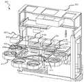
[0016] 하부(lower) 챔버 하우징 및 상부(upper) 챔버 하우징을 포함할 수 있는 결합 프로세싱 챔버(combination processing chamber)가 또한 설명된다. 하부 챔버 하우징은, 하부 챔버 하우징의 제 1 측(side) 상의 제 1 액세스(access), 및 하부 챔버 하우징의 제 1 측 맞은편의, 하부 챔버 하우징의 제 2 측 상의 제 2 액세스를 정의하거나 포함할 수 있다. 상부 챔버 하우징은 하부 챔버 하우징과 커플링될 수 있으며, 하부 챔버 하우징의 제 1 측과 일치하는(coinciding), 상부 챔버 하우징의 제 1 측 상의 제 3 액세스, 및 상부 챔버 하우징 내에 배치되는 페이스플레이트(faceplate)에 의해 상부(above)로부터 적어도 부분적으로 정의되는 상부 프로세싱 구역을 포함할 수 있다.
[0017] 하부 챔버 하우징은 하부(lower) 기판 구역을 정의할 수 있으며, 하부 기판 구역은, 하부 기판 구역을 약 300 ℃까지 가열하도록 구성된 히터를 또한 포함할 수 있거나, 히터에 의해 하부(below)로부터 적어도 부분적으로 정의될 수 있다. 하부 기판 구역은 또한, 대기압으로부터 대기압 아래의 제 2 압력으로 진공배기되도록(evacuated) 구성될 수 있으며, 하부 챔버 하우징은, 매 10분마다 대기압으로부터 약 5 mTorr 또는 그 미만으로 그리고 다시 대기압으로의 압력 사이클링을 구조적으로 지지하도록 구성될 수 있다.
[0018] 상부 프로세싱 챔버는 또한 온도 제어 디바이스를 포함할 수 있으며, 온도 제어 디바이스는 그 위에 배치된 기판의 온도를 약 0 ℃ 내지 약 600 ℃로 유지하도록 구성된다. 온도 제어 디바이스는, 상부 프로세싱 구역을 하부로부터 적어도 부분적으로 정의하기 위해, 상부 챔버 하우징 내에 배치되는 히터 플레이트를 포함할 수 있다. 상부 프로세싱 구역은 또한, 에지(edge) 구역을 따라 기판을 지지하고 그리고 상부 프로세싱 구역 내에 기판을 현수시키도록(suspend) 구성되는 기판 지지 디바이스를 포함할 수 있다. 챔버는 상부 챔버 하우징의 상부 부분과 커플링되는 원격 플라즈마 유닛을 가질 수 있다. 페이스플레이트와 상부 챔버 하우징의 상부 부분 사이에 적어도 부분적으로 정의되는 상부 분배 구역이 또한 포함될 수 있다. 상부 분배 구역은, 중심 분배 구역, 및 중심 분배 구역으로부터 파티셔닝되며(partitioned) 그리고 중심 분배 구역에 대해 방사상으로 말단에 있는(radially distal) 에지 분배 구역을 포함할 수 있다.
[0019] 결합 챔버는, 상부 챔버 하우징의 상부 부분 내에 포지셔닝되며 그리고 상부 분배 구역 내로 전구체들을 전달하도록 구성되는 가스 유입구 어셈블리(gas inlet assembly)를 더 포함할 수 있다. 가스 유입구 어셈블리는 원통형 형상에 의해 적어도 부분적으로 특징화될 수 있으며, 가스 유입구 어셈블리의 하부 부분이, 가스 유입구 어셈블리의 하부 부분 주위에 방사상으로 분배되는 복수의 가스 전달 애퍼처들(apertures)을 정의할 수 있다. 가스 유입구 어셈블리는 또한, 가스 유입구 어셈블리의 원통형 형상 부분 둘레에 적어도 하나의 전구체를 전달하도록 구성되는 바이패스 유체 채널을 포함할 수 있다. 바이패스 유체 채널은 적어도 하나의 전구체를 중심 분배 구역으로 지향시키도록 구성되는 제 1 바이패스 섹션을 포함할 수 있으며, 바이패스 유체 채널은 적어도 하나의 전구체를 에지 분배 구역으로 지향시키도록 구성되는 제 2 바이패스 섹션을 포함할 수 있다.
[0020] 결합 챔버의 페이스플레이트는, 교번적인 스위치 포지션들에서 전기 전력 소스 및 접지 소스에 페이스플레이트를 연결하도록 동작가능한 다중-포지션 스위치와 커플링될 수 있다. 상부 챔버 하우징의 하부 부분은, 페이스플레이트가 전기 전력 소스에 연결될 때 상부 프로세싱 구역에서 플라즈마가 생성되도록, 접지될 수 있다. 상부 챔버 하우징의 하부 부분은 또한, 상부 챔버 하우징의 나머지로부터 전기적으로 격리될 수 있다.
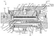
[0021] 개시되는 기술은 또한 처리 챔버를 포함할 수 있다. 처리 챔버는, 기판 로드 록 챔버와 커플링되는 바닥 부분을 갖는 챔버 하우징을 포함할 수 있다. 처리 챔버는 또한, 챔버 내에 정의되는 내부 구역에 유체들을 수용하도록 구성되는 유입구 어셈블리, 및 내부 구역 내에 배치되며 그리고 챔버 내에서 상부로부터 프로세싱 구역을 정의하고 하부로부터 분배 구역을 정의하는 페이스플레이트를 포함할 수 있다.
[0022] 페이스플레이트는 석영과 같은 유전체 재료를 포함할 수 있으며, 그리고 페이스플레이트가 전극으로서 동작할 수 있도록 전도성 재료를 또한 포함할 수 있다. 그러한 구성에서, 챔버는 프로세싱 구역에서 플라즈마를 생성하도록 구성될 수 있다. 챔버의 컴포넌트들은 라이닝되거나(lined) 또는 다른 방식으로(otherwise) 처리될 수 있으며, 유입구 어셈블리는, 예를 들어, 석영 라이너를 포함할 수 있다. 처리 챔버는 또한, 유입구 어셈블리와 커플링되는 에너지 생성 유닛(energy production unit)을 가질 수 있다. 유입구 어셈블리는 또한 윈도우(window)를 포함할 수 있으며, 그리고 에너지 생성 유닛은 챔버 내로 자외선 광(ultraviolet light)을 제공하도록 구성되는 광 소스를 포함할 수 있다.
[0023] 개시되는 기술은 또한, 처리된 기판 상에서의 표면 반응들을 방지하는 방법들을 포함할 수 있다. 방법들은 제 1 에칭 프로세스에서 기판을 에칭하는 단계를 포함할 수 있으며, 제 1 에칭 프로세스는 실리콘보다 실리콘 산화물에 대해 선택적일 수 있다. 방법들은 또한 제 2 에칭 프로세스에서 기판을 에칭하는 단계를 포함할 수 있으며, 제 2 에칭 프로세스는 실리콘 산화물보다 실리콘에 대해 선택적일 수 있다. 방법들은 기판을 제 1 처리 온도로 가열하는 단계, 및 그 후 기판을 무-수분 환경(moisture-free environment)으로 이송하는 단계를 포함할 수 있다.
[0024] 기판을 가열한 후에, 기판은 챔버로 이송될 수 있으며, 그리고 무-수분 환경을 유지하기 위해, 챔버를 통하여 유체가 연속으로 유동될 수 있다. 에칭 프로세스들에 대해, 제 2 에칭 프로세스는 불소-함유 전구체 및 산소-함유 전구체를 포함할 수 있다. 제 1 에칭 프로세스는 불소-함유 전구체 및 수소-함유 전구체를 활용할 수 있다. 에칭 프로세스들에서, 실리콘 산화물의 구역이 제 2 에칭 프로세스에 노출될 수 있으며, 제 2 에칭 프로세스는 라디칼 불소 종을 생성할 수 있다. 이러한 잔류 불소 종은, 실리콘 산화물 또는 다른 노출된 재료들, 이를 테면 실리콘 질화물에 혼입될(incorporated) 수 있다. 가열 동작을 위한 제 1 온도는 약 150 ℃ 또는 그 초과일 수 있다. 이 동작들은 마찬가지로, 기판을 제 1 온도 초과의 또는 제 1 온도 미만의 제 2 온도로 가열하는 것을 포함할 수 있다. 기판은 제 1 시간 기간 동안 제 1 온도로 유지될 수 있으며, 제 1 시간 기간은 약 2분 또는 그 초과이다. 제 2 가열 동작이 수행되는 경우, 기판은, 제 1 시간 기간 초과 또는 제 1 시간 기간 미만일 수 있는 제 2 시간 기간 동안 제 2 온도로 유지될 수 있다.
[0025] 실리콘을 포함하며 그리고 실리콘 위에 놓이는 실리콘 산화물 층을 갖는 기판을 제공하는 단계를 포함할 수 있는, 기판을 에칭하는 방법들이 또한 포함된다. 방법들은 제 1 에칭 프로세스에서 기판을 에칭하는 단계를 포함할 수 있으며, 제 1 에칭 프로세스는 실리콘보다 실리콘 산화물에 대해 선택적일 수 있다. 기판은 제 2 에칭 프로세스에서 에칭될 수 있으며, 제 2 에칭 프로세스는 실리콘 산화물보다 실리콘에 대해 선택적일 수 있다. 방법들은 또한, 제 3 에칭 프로세스에서 기판을 에칭하는 단계를 포함할 수 있으며, 제 3 에칭 프로세스는 실리콘보다 실리콘 산화물에 대해 선택적일 수 있다. 개시된 실시예들에서, 제 1 및 제 3 에칭 프로세스들은 유사한 에칭 프로세스들이다. 제 1 및 제 3 에칭 프로세스들은 제 1 프로세스 챔버에서 수행될 수 있으며, 제 2 에칭 프로세스는 제 2 프로세스 챔버에서 수행될 수 있다. 제 3 에칭 프로세스는, 잔류 할로겐화물 종을 포함할 수 있는 적어도 약 5Å의 깊이의 재료를 제거하기 위해 실리콘 산화물 층을 에칭할 수 있다. 제 1 및 제 3 에칭 프로세스들은, 질소-함유 전구체 및 불소-함유 전구체에 기판을 노출시키는 단계를 포함할 수 있으며, 불소-함유 전구체는 플라즈마 배출물들(effluents)을 생성하기 위해 플라즈마를 통해 유동되었다. 제 2 에칭 프로세스는 불소-함유 전구체 및 산소-함유 전구체에 기판을 노출시키는 단계를 포함하며, 불소-함유 전구체는 플라즈마 배출물들을 생성하기 위해 플라즈마를 통해 유동되었다. 실리콘 산화물 층은 제 2 에칭 프로세스에 노출될 수 있으며, 잔류 불소 종이 실리콘 산화물 층에 혼입될 수 있다.
[0026] 실리콘을 포함하며 그리고 실리콘 위에 놓이는 실리콘 산화물 층을 갖는 기판을 제공하는 단계를 또한 포함할 수 있는, 기판을 에칭하는 부가적인 방법들이 포함된다. 프로세스는 제 1 에칭 프로세스에서 기판을 에칭하는 단계를 포함할 수 있으며, 제 1 에칭 프로세스는 실리콘보다 실리콘 산화물에 대해 선택적일 수 있다. 방법들은 제 2 에칭 프로세스에서 기판을 에칭하는 단계를 포함할 수 있으며, 제 2 에칭 프로세스는 실리콘 산화물보다 실리콘에 대해 선택적일 수 있다. 방법들은 또한, 제 3 프로세스를 이용하여 기판을 처리하는 단계를 포함할 수 있다. 실리콘 산화물 층은 프로세싱 동안, 제 2 에칭 프로세스에 노출될 수 있다. 제 2 에칭 프로세스는 라디칼 불소 종을 생성할 수 있으며, 잔류 불소 종은, 특정 프로세스들에서 실리콘 산화물 층에 혼입될 수 있다.
[0027] 설명된 방법들 중 제 3 프로세스는, 기판의 표면에 플라즈마 배출물들을 지향시키는 단계를 포함할 수 있다. 플라즈마 배출물들은 비활성 전구체로부터 생성될 수 있으며, 실리콘 산화물 층으로부터 상단 표면(top surface)을 제거할 수 있다. 개시된 실시예들에서, 제 3 프로세스는 습식 에칭 프로세스를 포함할 수 있다. 특정 구성들에서, 제 1, 제 2, 및 제 3 프로세스들 중 각각의 프로세스는 상이한 프로세스 챔버들에서 수행될 수 있다. 습식 에칭은 불화수소산(hydrofluoric acid), 이를 테면, 특정 실시예들에서, 200:1, 150:1, 100:1, 50:1 등, 또는 나열된(listed) 것들 이내의, 초과의, 또는 미만의, 다른 비율들일 수 있는 DHF를 포함할 수 있다. 습식 에칭은 약 12Å까지의 실리콘 산화물 층을 제거할 수 있다. 개시된 실시예들에서, 제 3 프로세스는 실리콘 산화물 층을 탈이온수에 노출시키는 단계를 포함할 수 있다. 탈이온수는, 실리콘 산화물 층을 에칭하지 않으면서, 실리콘 산화물 층으로부터 잔류 불소 종의 적어도 일부를 제거할 수 있다.
[0028] 본 발명의 기술은 또한, 노출된 실리콘 및 실리콘 산화물 표면들을 갖는 프로세싱된 기판으로부터 오염물질들을 제거하는 방법들을 포함한다. 방법들은 에칭 프로세스에서 기판을 에칭하는 단계를 포함할 수 있으며, 에칭 프로세스는 실리콘 산화물보다 실리콘에 대해 선택적일 수 있다. 에칭 프로세스는 라디칼 종을 생성할 수 있으며, 라디칼 종으로부터의 잔류 종은 실리콘 산화물 층에 혼입될 수 있다. 방법들은 또한, 실리콘 산화물 표면으로부터 잔류 종의 적어도 일부를 제거하도록 기판을 처리하는 단계를 포함할 수 있다. 수행되는 에칭 프로세스는 불소-함유 전구체 및 산소-함유 전구체에 기판을 노출시키는 단계를 포함할 수 있다. 불소-함유 전구체는, 라디칼 불소 종을 포함할 수 있는 라디칼 종의 적어도 일부를 생성하기 위해 플라즈마를 통해 유동되었을 수 있다.
[0029] 에칭 프로세스는 실리콘 산화물 층을 에칭하지 않을 수 있거나, 실질적으로 에칭하지 않을 수 있다. 예를 들어, 실리콘 산화물 재료의 단지 약간의 제거 만이 일어날 수 있다. 라디칼 불소 종은, 실리콘 산화물 막의 깊이들이 증가함에 따라 혼입(incorporation)의 정도가 감소되는 프로파일(profile)로, 실리콘 산화물 층에 혼입될 수 있다. 수행될 수 있는 처리는, 열 처리, UV 처리, e-빔 처리, 마이크로파 처리, 경화 처리 및 플라즈마 처리로 이루어진 그룹으로부터 선택될 수 있다. 처리가 수행될 수 있는 온도는 약 0 ℃ 내지 약 800 ℃의 온도일 수 있다. 부가적으로, 처리가 수행될 수 있는 압력은 약 1 mTorr 내지 약 700 Torr의 압력일 수 있다. 기판을 처리하는 단계는, 실리콘 산화물 층 내의 잔류 종의 양을 약 20% 또는 그 미만으로 감소시키는 단계를 포함할 수 있다. 기판을 처리하는 단계는 또한, 실리콘 산화물 층 내의 잔류 종의 양을 약 10% 또는 그 미만, 또는 약 5% 또는 그 미만으로 감소시키는 단계를 포함할 수 있다. 개시된 실시예들에서, 그러한 처리는 실리콘 산화물 재료의 상부 표면에서 잔류 할로겐화물을 실질적으로 또는 본질적으로 제거할 수 있다. 그러한 경우들에서, 실리콘 산화물 표면의 더 낮은 깊이들(lower depths)에서는 잔류 할로겐화물 종이 여전히 존재할 수 있다.
[0030] 방법들은 또한, 처리 프로세스를 위해 기판을 처리 챔버에 이송하는 단계를 포함할 수 있다. 기판은 처리 챔버로의 이송 동안에 진공 하에서 유지될 수 있고, 기판을 처리하는 것은, 라디칼 종과 상호작용하도록 구성된 에너자이징된 처리 종을 생성하기 위해, 에너지 소스에 처리 종을 노출시키는 것을 포함할 수 있다. 개시된 실시예들에서, 처리 종은, 수소-함유 전구체들, 산소-함유 전구체들, 질소-함유 전구체들 및 비활성 전구체들로 구성된 그룹으로부터 선택될 수 있고, 일 예에서, 처리 종을 에너자이징하기 위해 사용되는 에너지 소스는, 기판에 에너자이징된 종을 전달하기 위해 처리 챔버 내에서 또는 외부에서 형성될 수 있는 플라즈마를 포함할 수 있다. 내부적으로 또는 외부적으로 활용되는 플라즈마는, 용량성으로-결합된 플라즈마, 유도적으로 결합된 플라즈마, 마이크로파 플라즈마, 및 토로이달(toroidal) 플라즈마로 구성된 그룹으로부터 선택되는 플라즈마를 포함할 수 있다. 활용되는 처리 종은, 잔류 종과 결합하는 수소-함유 전구체를 포함하는 하나 또는 그 초과의 전구체들을 포함할 수 있다. 방법들은 또한, 패시베이션 프로세스를 위해 패시베이션 챔버에 기판을 이송하는 단계를 포함할 수 있다. 패시베이션이 일어나는 챔버로의 이송 동안에, 기판은 진공 하에서 또는 비활성 환경 내에서 유지될 수 있다. 수행되는 패시베이션은, 약 2 분 또는 그 초과의 시간 기간 동안, 약 150 ℃ 또는 그 초과의 온도로 기판을 가열하는 것을 포함할 수 있다.
[0031] 개시되는 기술은 또한, 노출된 실리콘 산화물 구역 및 노출된 비-산화물 구역을 갖는 기판 상에서 오염물질들을 제거하는 방법들을 포함할 수 있다. 방법들은, 기판 프로세싱 챔버의 기판 프로세싱 구역과 유체적으로(fluidly) 커플링된, 기판 프로세싱 챔버의 원격 플라즈마 구역 내로 불소-함유 전구체를 유동시키면서, 원격 플라즈마 구역에서 플라즈마를 형성하여, 불소-함유 플라즈마 배출물들을 생성하는 단계를 포함할 수 있다. 방법들은, 플라즈마 배출물들을 활용하여, 노출된 비-산화물 구역을 에칭하는 단계를 포함할 수 있고, 불소-함유 플라즈마 배출물들의 부분을 구성하는 불소 종은, 에칭 프로세스 동안에 노출될 수 있는 실리콘 산화물 구역에 혼입될 수 있다. 방법들은, 처리 플라즈마 배출물들을 생성하기 위해, 기판 프로세싱 챔버의 원격 플라즈마 구역 내로 제 1 처리 전구체를 유동시키는 단계, 및 처리 플라즈마 배출물들과 상호작용할 수 있는 적어도 하나의 부가적인 처리 전구체를 기판 프로세싱 구역 내로 유동시키는 단계를 포함할 수 있다. 방법들은, 실리콘 산화물 구역으로부터 잔류 플라즈마 배출물들을 제거하기 위해, 처리 플라즈마 배출물들을 포함하는 처리 전구체들에 실리콘 산화물 구역을 노출시키는 단계를 더 포함할 수 있다.
[0032] 개시된 실시예들에서, 기판의 노출된 비-산화물 구역은 실리콘, 실리콘 질화물, 또는 금속을 포함할 수 있다. 사용될 수 있는 처리 플라즈마 배출물들은, 기판 프로세싱 구역에서 적어도 하나의 부가적인 처리 전구체를 적어도 부분적으로 해리시킬 수 있다. 전구체를 적어도 부분적으로 해리시킴으로써, 부분적으로 해리된 종의 조합들 사이의 완전히 해리된 종이 형성될 수 있다. 적어도 부분적으로 해리된 적어도 하나의 부가적인 처리 전구체는, 실리콘 산화물 구역에 혼입된 불소 종과, 물리적으로 또는 화학적으로 상호작용할 수 있고, 그 불소 종과 결합할 수 있다. 처리 전구체는 비활성 또는 노블(noble) 종을 포함할 수 있으며, 그리고 질소, 헬륨, 아르곤, 및 크세논으로 구성된 그룹으로부터 선택되는 전구체를 포함할 수 있다.
[0033] 활용되는 적어도 하나의 부가적인 처리 전구체는, 다른 전구체들 중에서, 수소-함유 전구체를 포함할 수 있다. 실리콘 산화물 재료에 대해 수행되는 노출은 실리콘 산화물 재료의 부분이 제거되게 할 수 있다. 노출은 또한, 실리콘 산화물 재료를 유지 또는 본질적으로 유지하면서, 불소 종의 적어도 일부를 제거할 수 있다. 따라서, 실리콘 산화물 종의 약간의 의도하지 않은 제거가 여전히 방법들에 의해 포함될 수 있다. 방법들은 단일 챔버 환경에서 수행될 수 있고, 이는, 방법들이, 챔버 내의 안정적인 또는 일정한 환경에서, 뿐만 아니라, 실질적으로 진공배기된 환경에서 발생되게 허용할 수 있다. 노출은, 범위 내의 다수의 온도들 중에서, 약 0 ℃ 내지 약 800 ℃의 온도에서 수행될 수 있고, 노출은 또한, 다양한 포함된 압력들 중에서, 약 1 mTorr 내지 약 700 Torr의 압력에서 수행될 수 있다.
[0034] 본 기술은 여전히, 노출된 실리콘 산화물 구역 및 노출된 비-산화물 구역을 갖는 기판 상에서 오염물질들을 제거하는 방법들을 더 포함할 수 있다. 방법들은, 기판 프로세싱 챔버의 기판 프로세싱 구역과 유체적으로 커플링된, 기판 프로세싱 챔버의 원격 플라즈마 구역 내로 불소-함유 전구체를 유동시키면서, 원격 플라즈마 구역에서 플라즈마를 형성하여, 불소-함유 플라즈마 배출물들을 생성하는 단계를 포함할 수 있다. 방법들은, 플라즈마 배출물들을 활용하여, 노출된 비-산화물 구역을 에칭하는 단계를 더 포함할 수 있고, 여기에서, 잔류 불소 종은 실리콘 산화물 구역 내에 혼입될 수 있다. 방법들은, 기판 프로세싱 구역 내로 적어도 하나의 처리 전구체를 유동시는 단계 뿐만 아니라, 적어도 하나의 처리 전구체에 실리콘 산화물 구역을 노출시켜서, 잔류 불소 종의 적어도 일부를 제거하는 단계를 더 포함할 수 있다.
[0035] 적어도 하나의 처리 전구체는, 기판 프로세싱 구역 내로 유동되기 전에, 플라즈마를 통해 통과되지 않을 수 있고, 개시된 실시예들에서, 프로세싱 구역은 노출 동안에 무 플라즈마(plasma free)로 유지될 수 있다. 따라서, 개시된 실시예들에서, 처리 동작은 완전히 또는 실질적으로 무 플라즈마로 수행될 수 있다. 유동 동작은, 실리콘 산화물 구역의 표면 상에 수증기를 응축시키는 것, 뿐만 아니라, 기판 프로세싱 구역 내로 질소-함유 전구체를 유동시키는 것을 포함할 수 있는 다수의 프로세스들을 포함할 수 있다. 이러한 단계들은 순차적으로 수행될 수 있고, 다이렉트 시퀀스(direct sequence)로, 또는 단계들 사이에서의 온도 및 압력을 포함하는 특정한 시스템 동작들의 조작 후에 수행될 수 있다. 처리 프로세스에서 사용되는 질소-함유 전구체는 암모니아를 포함할 수 있다.
[0036] 처리 동안에, 수증기는 잔류 불소 종과 상호작용할 수 있다. 이는, 표면 내의 잔류 종의 혼입 또는 결합을 방해할 수 있고, 응축된 물의 컴포넌트들과의 직접 결합(direct bonding)을 위한 것일 수 있다. 그 후에, 실리콘 산화물 구역을 따라 부산물들을 생성하기 위해, 암모니아가 재료 또는 조합된 재료들과 상호작용할 수 있다. 방법들은, 부산물들이 증발되게 할 수 있는 임계치 온도 위로, 챔버 내의 온도를 상승시키는 단계를 더 포함할 수 있다. 개시된 실시예들에서, 임계치 온도는, 예를 들어, 약 100 ℃ 초과일 수 있다. 개시된 실시예들에서, 프로세스가 실리콘 산화물 층을 최소한으로 감소시킬 수 있지만, 프로세스는 또한, 실리콘 산화물 재료를 실질적으로 또는 본질적으로 유지할 수 있고, 그에 따라, 재료의 두께가 감소되지 않거나, 또는 약 50%, 40%, 30%, 25%, 20%, 15%, 10%, 5%, 1% 등 또는 그 미만과 같은 특정 레벨 아래로 감소되거나, 또는 전혀 제거되지 않는다. 본 개시 전반에 걸쳐 설명되는 바와 같은 다른 방법들 및 기법들은, 유사하게, 재료의 전체 두께를 본원에서 정의되는 레벨들 중 임의의 것으로 감소시킬 수 있다. 프로세스는 또한, 실리콘 산화물의 표면 층 내의 불소의 농도를 약 10% 아래로 감소시킬 수 있고, 이는, 잔류 불소 종을 포함하는 상당량(an amount of)의 실리콘 산화물 재료를 제거하는 것을 포함할 수 있거나, 또는 실리콘 산화물 재료로부터 불소 종을 제거하는 것일 수 있다.
[0037] 그러한 기술은 종래의 기법들에 비해 다수의 이익들을 제공할 수 있다. 예를 들어, 시스템들 및 프로세스들은, 무-수분 환경을 유지하면서 처리 프로세스들이 수행되게 허용하는 새로운 챔버들에 의한 부가적인 기능성을 제공할 수 있다. 프로세스들 및 시스템들은 또한, 기판들 상의 에이징 결함들을 제한하고, 그리고/또는 근본적인 원인들을 제거하는 개선된 프로세스들을 제공할 수 있다. 이들 및 다른 실시예들은, 이들의 이점들 및 피쳐들 중 다수와 함께, 아래의 설명 및 첨부된 도면들과 함께 더 상세히 설명된다.Systems, chambers, and processes are provided for controlling process defects caused by moisture contamination. Systems may provide configurations for allowing chambers to perform multiple operations in a vacuum or controlled environment. Chambers may include configurations to provide additional processing capabilities in combination chamber designs. The methods can provide limiting, prevention, and correction of aging defects that may be caused as a result of etching processes performed by system tools.
[0007] Substrate processing systems according to the present technology include a plurality of holding chambers; A plurality of loading chambers configured to receive substrates into the vacuum environment; And an interface section i having at least two interface transfer devices, wherein the at least two interface transfer devices include a plurality of holding chambers coupled with the interface section at a first position of the interface section, and a plurality of Is configured to transfer substrates between a plurality of loading chambers coupled with the interface section at a second location of the interface section, opposite of the holding chambers of the. The systems may also include a treatment chamber coupled with at least one of the plurality of loading chambers and positioned vertically aligned with such at least one loading chamber. The systems are configured to transfer a substrate between a plurality of process chambers, as well as any of the plurality of processing chambers and any of the plurality of loading chambers, while maintaining the substrate under vacuum conditions. It may include a device. The process transfer device can also be configured to transfer substrates vertically to the processing chamber.
[0008] Processing systems may have all of the loading chambers and process chambers on a first elevation plane of the system, and a processing chamber above the first elevation plane of the substrate processing system. Can have on the second height plane of the system. The transfer device can be configured to maintain vacuum conditions while transferring substrates vertically to the processing chamber. Systems may include a plurality of processing chambers, each processing chamber coupled with and vertically aligned to one of the plurality of loading chambers. The systems can also include two loading chambers and two processing chambers, and the loading chambers can be placed horizontally with each other.
The systems may further include a processing plasma generating device that is separate from both of the processing chambers and coupled with both of the processing chambers. The systems may also include two processing plasma generating devices, one of the processing plasma generating devices may be coupled with one of the processing chambers, and a second of the processing plasma generating devices is one of the processing chambers. It can be coupled with the second processing chamber. The processing chamber may include components configured to generate a direct plasma within the processing chamber, and the direct plasma may include a capacitively-coupled plasma. The processing chamber may also include components configured to generate ultraviolet light treatment within the processing chamber. The holding chambers of the systems may include at least one inlet port and may be configured to receive fluid through the inlet port, and to direct fluid through the holding chamber into the interface section. The holding chambers may also include at least one internal diffuser configured to direct the contained fluid throughout the holding chamber. System loading chambers may include at least one heating device configured to heat the loading chamber to about 300°C.
The processing systems may further include a wet etch chamber coupled with the interface section at a third location of the interface section, adjacent to the first location and the second location of the interface section. The storage chamber can also be coupled with the interface section in a fourth position of the interface section, opposite the third position.
[0011] Processing chambers of processing systems may be coupled as pairs of tandem processing chambers within a substrate processing system. The processing chamber may include at least two pairs of tandem processing chambers, and a first pair of at least two pairs of tandem processing chambers may be configured to perform a silicon oxide etching operation, and at least two pairs of tandem processing chambers The second pair of chambers may be configured to perform a silicon etching operation.
Methods of processing a substrate are also described, and the methods may include transferring a substrate from a holding chamber to a loading chamber using a first transfer device. The methods may also include evacuating the loading chamber such that the substrate is maintained in a vacuum environment. The methods include transferring a substrate from an evacuated loading chamber to a process chamber, using a second transfer device, and thereafter, transferring a substrate from the process chamber to a loading chamber, using a second transfer device. Can include. Once returned to the loading chamber, the methods may include removing vacuum conditions from the loading chamber, and finally, transferring the substrate from the loading chamber to the storage chamber using a first transfer device. I can.
The methods may also include transferring the substrate to a wet etch station using the first transfer device prior to transferring the substrate to the holding chamber. The methods may further include, prior to transferring the substrate to the loading chamber, using a second transfer device to transfer the substrate from the process chamber to a processing chamber coupled with the loading chamber and vertically aligned with the loading chamber. have. The processing chamber of the methods may be configured to perform a scavenging operation to remove halide species from the silicon oxide material. In disclosed embodiments, the scavenging operation may include a plasma process, and may also include a UV treatment or an e-beam treatment.
[0014] The storage chamber may be continuously purged with an inert fluid such that the storage chamber includes an inert environment, and in disclosed embodiments, the storage chamber may be a holding chamber, but also , The storage chamber may be a chamber separate from the holding chamber. The methods may also include heating the substrate to a first temperature for a first period of time after transferring the substrate to the loading chamber. The process chamber can include a first process chamber, and the first process chamber can be configured to perform an oxide etch process. The methods can also include transferring the substrate from the first process chamber to the second process chamber prior to transferring the substrate to the loading chamber, and the second process chamber can be configured to perform a silicon etch process. .
[0015] A computing system electronically coupled to the substrate processing system and configured to provide operational instructions to the substrate processing system is also described. A computing system may include one or more processors and a memory device communicatively coupled with the one or more processors and having sets of instructions for performing operations. When sets of instructions are executed by one or more processors, those sets of instructions cause the substrate processing system and/or gas delivery system and individual chambers to hold the substrate from the holding chamber using the first transfer device. It may be possible to be instructed to transfer to the loading chamber. The instructions may additionally cause the loading chamber to be evacuated so that the substrate can be held in a vacuum environment. The instructions also include transfer of the substrate from the evacuated loading chamber to the process chamber using the second transfer device, as well as from the process chamber, using the second transfer device, coupled with the loading chamber and vertically aligned with the loading chamber It may cause the transfer of the substrate to the processing chamber. The instructions executed may additionally cause the transfer of the substrate from the processing chamber to the loading chamber using a second transfer device, followed by removal of vacuum conditions from the loading chamber. The instructions executed may additionally cause the transfer of the substrate from the loading chamber to the holding chamber using the first transfer device. The computer system, which may be a controller, may also be electronically coupled with the gas delivery system and configured to provide instructions to the gas delivery system, and cause the gas delivery system to provide at least one precursor to the process chamber. I can do it. When the substrate has been transferred back to the loading chamber, the instructions may cause the processing system to heat the loading chamber from a first temperature to a second temperature of about 200° C. or higher.
[0016] A combination processing chamber, which may include a lower chamber housing and an upper chamber housing, is also described. The lower chamber housing may define or include a first access on a first side of the lower chamber housing and a second access on a second side of the lower chamber housing opposite the first side of the lower chamber housing. I can. The upper chamber housing may be coupled with the lower chamber housing, coinciding with the first side of the lower chamber housing, a third access on the first side of the upper chamber housing, and a faceplate disposed within the upper chamber housing ( It may comprise an upper processing region defined at least in part from above by a faceplate.
[0017] The lower chamber housing may define a lower substrate region, and the lower substrate region may also include a heater configured to heat the lower substrate region to about 300° C., or be lower by the heater. Can be at least partially defined from The lower substrate region may also be configured to be evacuated from atmospheric pressure to a second pressure below atmospheric pressure, the lower chamber housing being at a pressure of about 5 mTorr or less from atmospheric pressure and back to atmospheric pressure every 10 minutes. It can be configured to structurally support cycling.
[0018] The upper processing chamber may also include a temperature control device, the temperature control device being configured to maintain a temperature of a substrate disposed thereon between about 0° C. and about 600° C. The temperature control device may comprise a heater plate disposed within the upper chamber housing to at least partially define the upper processing region from below. The upper processing region may also include a substrate support device configured to support the substrate along the edge region and suspend the substrate within the upper processing region. The chamber can have a remote plasma unit coupled with an upper portion of the upper chamber housing. An upper dispensing zone may also be included that is defined at least partially between the faceplate and the upper portion of the upper chamber housing. The upper distribution zone may comprise a central distribution zone and an edge distribution zone partitioned from the central distribution zone and radially distal to the central distribution zone.
[0019] The bonding chamber may further include a gas inlet assembly positioned within the upper portion of the upper chamber housing and configured to deliver precursors into the upper dispensing zone. The gas inlet assembly may be characterized at least in part by a cylindrical shape, wherein the lower portion of the gas inlet assembly may define a plurality of gas delivery apertures distributed radially around the lower portion of the gas inlet assembly. I can. The gas inlet assembly may also include a bypass fluid channel configured to deliver at least one precursor around a cylindrically shaped portion of the gas inlet assembly. The bypass fluid channel can include a first bypass section configured to direct at least one precursor to the central dispensing region, wherein the bypass fluid channel is configured to direct at least one precursor to the edge dispensing region. It may include 2 bypass sections.
[0020] The faceplate of the coupling chamber may be coupled with a multi-position switch operable to connect the faceplate to an electrical power source and a ground source in alternating switch positions. The lower portion of the upper chamber housing can be grounded so that plasma is generated in the upper processing region when the faceplate is connected to an electrical power source. The lower portion of the upper chamber housing can also be electrically isolated from the rest of the upper chamber housing.
[0021] The disclosed technology may also include a processing chamber. The processing chamber may include a chamber housing having a bottom portion coupled with a substrate load lock chamber. The processing chamber also includes an inlet assembly configured to receive fluids in an interior zone defined within the chamber, and a faceplate disposed within the interior zone and defining a processing zone from above and a dispensing zone from the bottom within the chamber I can.
[0022] The faceplate may comprise a dielectric material such as quartz, and may also comprise a conductive material such that the faceplate can act as an electrode. In such a configuration, the chamber can be configured to generate a plasma in the processing region. The components of the chamber may be lined or otherwise treated, and the inlet assembly may include, for example, a quartz liner. The processing chamber can also have an energy production unit coupled with the inlet assembly. The inlet assembly may also include a window, and the energy generating unit may include a light source configured to provide ultraviolet light into the chamber.
[0023] The disclosed technique may also include methods of preventing surface reactions on a treated substrate. The methods may include etching the substrate in a first etching process, and the first etching process may be selective for silicon oxide over silicon. The methods may also include etching the substrate in a second etching process, and the second etching process may be selective for silicon over silicon oxide. The methods may include heating the substrate to a first processing temperature, and then transferring the substrate to a moisture-free environment.
After heating the substrate, the substrate can be transferred to the chamber, and fluid can be continuously flowed through the chamber to maintain a moisture-free environment. For etching processes, the second etching process may include a fluorine-containing precursor and an oxygen-containing precursor. The first etching process may utilize a fluorine-containing precursor and a hydrogen-containing precursor. In etching processes, a region of silicon oxide may be exposed to a second etching process, and the second etching process may generate radical fluorine species. These residual fluorine species can be incorporated into silicon oxide or other exposed materials, such as silicon nitride. The first temperature for the heating operation may be about 150° C. or higher. These operations may likewise include heating the substrate to a second temperature above the first temperature or below the first temperature. The substrate may be maintained at a first temperature during a first period of time, the first period of time being about 2 minutes or more. When the second heating operation is performed, the substrate may be maintained at the second temperature for a second time period, which may be greater than or less than the first time period.
Also included are methods of etching a substrate that include silicon and may include providing a substrate having a silicon oxide layer overlying the silicon. The methods may include etching the substrate in a first etching process, and the first etching process may be selective for silicon oxide over silicon. The substrate may be etched in a second etch process, and the second etch process may be selective for silicon over silicon oxide. The methods may also include etching the substrate in a third etch process, and the third etch process may be selective for silicon oxide over silicon. In the disclosed embodiments, the first and third etching processes are similar etching processes. The first and third etching processes may be performed in the first process chamber, and the second etching process may be performed in the second process chamber. The third etch process may etch the silicon oxide layer to remove material to a depth of at least about 5 Angstroms that may contain residual halide species. The first and third etching processes may include exposing the substrate to a nitrogen-containing precursor and a fluorine-containing precursor, the fluorine-containing precursor being flowed through the plasma to create plasma effluents. . The second etching process included exposing the substrate to a fluorine-containing precursor and an oxygen-containing precursor, the fluorine-containing precursor flowing through the plasma to produce plasma emissions. The silicon oxide layer may be exposed to a second etching process, and residual fluorine species may be incorporated into the silicon oxide layer.
[0026] Additional methods of etching a substrate are included that include silicon and may also include providing a substrate having a silicon oxide layer overlying the silicon. The process may include etching the substrate in a first etching process, and the first etching process may be selective for silicon oxide over silicon. The methods may include etching the substrate in a second etching process, and the second etching process may be selective for silicon over silicon oxide. The methods may also include processing the substrate using a third process. During processing, the silicon oxide layer may be exposed to a second etching process. The second etching process can produce radical fluorine species, and residual fluorine species can be incorporated into the silicon oxide layer in certain processes.
[0027] A third of the described methods may include directing plasma emissions to a surface of a substrate. Plasma emissions can be generated from an inert precursor and can remove the top surface from the silicon oxide layer. In disclosed embodiments, the third process can include a wet etch process. In certain configurations, each of the first, second, and third processes may be performed in different process chambers. Wet etching is a hydrofluoric acid, such as, in certain embodiments, 200:1, 150:1, 100:1, 50:1, etc., or within, greater than, or less than those listed. Of, may include DHF, which may be in different ratios. Wet etching can remove up to about 12 angstroms of silicon oxide layers. In disclosed embodiments, the third process may include exposing the silicon oxide layer to deionized water. Deionized water can remove at least some of the residual fluorine species from the silicon oxide layer without etching the silicon oxide layer.
[0028] The technique of the present invention also includes methods of removing contaminants from a processed substrate having exposed silicon and silicon oxide surfaces. The methods may include etching the substrate in an etching process, and the etching process may be selective for silicon over silicon oxide. The etching process can generate radical species, and residual species from the radical species can be incorporated into the silicon oxide layer. The methods may also include treating the substrate to remove at least some of the residual species from the silicon oxide surface. The etching process performed may include exposing the substrate to a fluorine-containing precursor and an oxygen-containing precursor. The fluorine-containing precursor may have been flowed through the plasma to generate at least some of the radical species, which may include radical fluorine species.
[0029] The etching process may or may not substantially etch the silicon oxide layer. For example, only slight removal of the silicon oxide material can take place. The radical fluorine species may be incorporated into the silicon oxide layer as a profile in which the degree of incorporation decreases as the depths of the silicon oxide film increase. The treatment that can be performed may be selected from the group consisting of heat treatment, UV treatment, e-beam treatment, microwave treatment, curing treatment and plasma treatment. The temperature at which the treatment can be carried out may be a temperature of about 0 °C to about 800 °C. Additionally, the pressure at which the treatment can be performed may be a pressure of about 1 mTorr to about 700 Torr. Treating the substrate may include reducing the amount of residual species in the silicon oxide layer to about 20% or less. Treating the substrate may also include reducing the amount of residual species in the silicon oxide layer to about 10% or less, or about 5% or less. In disclosed embodiments, such treatment can substantially or essentially remove residual halides from the top surface of the silicon oxide material. In such cases, residual halide species may still be present at lower depths of the silicon oxide surface.
The methods may also include transferring the substrate to a processing chamber for a processing process. The substrate can be maintained under vacuum during transfer to the processing chamber, and processing the substrate can include exposing the processing species to an energy source to create an energized processing species configured to interact with the radical species. . In disclosed embodiments, the treatment species may be selected from the group consisting of hydrogen-containing precursors, oxygen-containing precursors, nitrogen-containing precursors and inert precursors, and in one example, to energize the treatment species. The energy source used may include a plasma that may be formed inside or outside the processing chamber to deliver the energized species to the substrate. Plasma utilized internally or externally may include a plasma selected from the group consisting of capacitively-coupled plasma, inductively coupled plasma, microwave plasma, and toroidal plasma. The treatment species utilized may include one or more precursors, including hydrogen-containing precursors that bind with residual species. The methods may also include transferring the substrate to the passivation chamber for a passivation process. During transfer to the chamber where passivation takes place, the substrate can be maintained under vacuum or in an inert environment. The passivation performed may include heating the substrate to a temperature of about 150° C. or more, for a period of time of about 2 minutes or more.
[0031] The disclosed technique may also include methods of removing contaminants on a substrate having an exposed silicon oxide region and an exposed non-oxide region. The methods include forming a plasma in a remote plasma region while flowing a fluorine-containing precursor into a remote plasma region of the substrate processing chamber fluidly coupled with the substrate processing region of the substrate processing chamber to form a fluorine-containing plasma. Generating emissions. The methods may include, utilizing plasma emissions, etching the exposed non-oxide zone, wherein the fluorine species making up a portion of the fluorine-containing plasma emissions are exposed to the silicon oxide zone that may be exposed during the etching process. May be mixed. The methods include flowing a first treatment precursor into a remote plasma region of a substrate processing chamber to produce treatment plasma emissions, and at least one additional treatment precursor capable of interacting with the treatment plasma emissions into the substrate processing region. It may include a step of flowing. The methods may further include exposing the silicon oxide region to treatment precursors comprising the treatment plasma emissions to remove residual plasma emissions from the silicon oxide region.
In disclosed embodiments, the exposed non-oxide region of the substrate may comprise silicon, silicon nitride, or metal. The processing plasma emissions that may be used may at least partially dissociate at least one additional processing precursor in the substrate processing region. By at least partially dissociating the precursor, a fully dissociated species can be formed between combinations of partially dissociated species. At least one additional treatment precursor that is at least partially dissociated can physically or chemically interact with, and bind with, the fluorine species incorporated in the silicon oxide zone. The treatment precursor may include an inert or noble species, and may include a precursor selected from the group consisting of nitrogen, helium, argon, and xenon.
The at least one additional processing precursor utilized may include, among other precursors, a hydrogen-containing precursor. The exposure performed on the silicon oxide material can cause portions of the silicon oxide material to be removed. The exposure can also remove at least some of the fluorine species while retaining or essentially retaining the silicon oxide material. Thus, some unintended removal of silicon oxide species can still be involved by methods. The methods may be performed in a single chamber environment, which may allow the methods to occur in a stable or constant environment within the chamber, as well as in a substantially evacuated environment. The exposure can be carried out at a temperature of about 0° C. to about 800° C., among a number of temperatures within the range, and the exposure can also be carried out at a pressure of about 1 mTorr to about 700 Torr, among various included pressures. have.
[0034] The present technology may still further include methods of removing contaminants on a substrate having an exposed silicon oxide region and an exposed non-oxide region. The methods form a plasma in a remote plasma region while flowing a fluorine-containing precursor into a remote plasma region of the substrate processing chamber, fluidly coupled with the substrate processing region of the substrate processing chamber, to produce fluorine-containing plasma emissions. It may include the step of. The methods may further include, utilizing plasma emissions, etching the exposed non-oxide zone, where residual fluorine species may be incorporated into the silicon oxide zone. The methods may further include flowing the at least one treatment precursor into the substrate processing region, as well as exposing the silicon oxide region to the at least one treatment precursor to remove at least some of the residual fluorine species.
The at least one treatment precursor may not pass through the plasma before flowing into the substrate processing region, and in disclosed embodiments, the processing region may remain plasma free during exposure. Thus, in the disclosed embodiments, the processing operation can be performed completely or substantially with no plasma. The flow operation may include a number of processes that may include condensing water vapor on the surface of the silicon oxide region, as well as flowing a nitrogen-containing precursor into the substrate processing region. These steps may be performed sequentially, in a direct sequence, or after manipulation of certain system operations including temperature and pressure between the steps. The nitrogen-containing precursor used in the treatment process may include ammonia.
During treatment, water vapor can interact with residual fluorine species. This may interfere with the incorporation or bonding of residual species in the surface, and may be for direct bonding with condensed water components. Thereafter, ammonia can interact with the material or combined materials to produce by-products along the silicon oxide zone. The methods may further include raising a temperature in the chamber above a threshold temperature that may cause byproducts to evaporate. In disclosed embodiments, the threshold temperature may be greater than about 100° C., for example. In the disclosed embodiments, although the process can reduce the silicon oxide layer to a minimum, the process can also substantially or essentially retain the silicon oxide material, so that the thickness of the material is not reduced, or about 50 It is reduced below a certain level, such as %, 40%, 30%, 25%, 20%, 15%, 10%, 5%, 1%, etc. or less, or is not removed at all. Other methods and techniques as described throughout this disclosure can similarly reduce the overall thickness of the material to any of the levels defined herein. The process may also reduce the concentration of fluorine in the surface layer of silicon oxide to below about 10%, which may include removing an amount of silicon oxide material comprising residual fluorine species or Or it may be to remove the fluorine species from the silicon oxide material.
Such a technique can provide a number of benefits over conventional techniques. For example, systems and processes can provide additional functionality with new chambers that allow treatment processes to be performed while maintaining a moisture-free environment. Processes and systems may also provide improved processes that limit aging defects on substrates and/or eliminate root causes. These and other embodiments, along with many of their advantages and features, are described in more detail in conjunction with the description below and the accompanying drawings.
[0038] 개시된 기술의 성질 및 이점들의 추가적인 이해가, 본 명세서의 나머지 부분들 및 도면들을 참조하여 실현될 수 있다.
[0039] 도 1a는, 개시된 기술에 따른 예시적인 프로세싱 시스템의 상면도를 도시한다.
[0040] 도 1b는, 개시된 기술에 따른 다른 예시적인 프로세싱 시스템의 상면도를 도시한다.
[0041] 도 2는, 개시된 기술에 따른 예시적인 프로세싱 시스템의 후부(rear) 투시도를 도시한다.
[0042] 도 3은, 개시된 기술에 따른, 시스템에서 사용하기 위한 예시적인 프로세싱 챔버의 단면 개략도를 도시한다.
[0043] 도 4a는, 개시된 기술에 따른 예시적인 프로세싱 챔버의 다른 단면 개략도를 도시한다.
[0044] 도 4b는, 도 4a에서 도시된 프로세싱 챔버의 컴포넌트들의 상세한 부분도를 도시한다.
[0045] 도 5는, 개시된 기술에 따른 예시적인 프로세싱 챔버의 다른 단면 개략도를 도시한다.
[0046] 도 6은, 개시된 기술에 따른 예시적인 프로세싱 챔버의 다른 단면 개략도를 도시한다.
[0047] 도 7은, 개시된 기술에 따른 샤워헤드의 저면도를 도시한다.
[0048] 도 8은, 개시된 기술에 따른 다른 샤워헤드의 저면도를 도시한다.
[0049] 도 9는, 개시된 기술에 따른 예시적인 프로세싱 시스템의 후부 투시도를 도시한다.
[0050] 도 10은, 개시된 기술에 따른 예시적인 프로세싱 시스템의 후부 투시도를 도시한다.
[0051] 도 11은, 개시된 기술에 따른 예시적인 프로세싱 시스템의 후부 투시도를 도시한다.
[0052] 도 12a는, 개시된 기술에 따른, 로딩 챔버와 커플링가능한 예시적인 프로세싱 챔버를 도시한다.
[0053] 도 12b는, 라인 A-A를 따르는, 도 12a에서 예시된 프로세싱 챔버의 단면 부분의 평면도를 도시한다.
[0054] 도 12c는, 라인 A-A를 따르는, 도 12a에서 예시된 프로세싱 챔버의 단면 부분의 다른 평면도를 도시한다.
[0055] 도 13은, 개시된 기술에 따른 예시적인 결합 프로세싱 및 로딩 챔버를 도시한다.
[0056] 도 14는, 개시된 기술에 따른 웨이퍼 운반의 예시적인 프로세스를 도시한다.
[0057] 도 15는, 개시된 기술에 따른 웨이퍼 운반을 예시하는 예시적인 시스템의 상면도를 도시한다.
[0058] 도 16은, 개시된 기술에 따른, 증착 및 에칭 프로세스들의 예시적인 방법을 도시한다.
[0059] 도 17은, 개시된 기술에 따른, 에칭 및 처리 프로세스들의 예시적인 방법을 도시한다.
[0060] 도 18은, 개시된 기술에 따른, 에칭 및 제거 프로세스들의 예시적인 방법을 도시한다.
[0061] 도 19는, 개시된 기술에 따른, 에칭 및 처리 프로세스들의 예시적인 방법을 도시한다.
[0062] 도 20은, 개시된 기술에 따른, 에칭 및 노출 프로세스들의 예시적인 방법을 도시한다.
[0063] 도 21은, 논의되는 동작들 중 하나 또는 그 초과를 수행하기 위해 활용될 수 있는 단순화된 컴퓨터 시스템을 도시한다.
[0064] 첨부된 도면들에서, 유사한 컴포넌트들 및/또는 피쳐들은 동일한 수치 참조 라벨을 가질 수 있다. 추가로, 동일한 타입의 다양한 컴포넌트들은, 참조 라벨 뒤에, 유사한 컴포넌트들 및/또는 피쳐들 사이를 구별하는 문자를 뒤따르게 함으로써 구별될 수 있다. 본 명세서에서 제 1 수치 참조 라벨만이 사용되는 경우에, 문자 첨자와 무관하게, 동일한 제 1 수치 참조 라벨을 갖는 유사한 컴포넌트들 및/또는 피쳐들 중 임의의 것에 대해 설명이 적용가능하다.[0038] A further understanding of the nature and advantages of the disclosed technology may be realized with reference to the remainder of the specification and drawings.
1A shows a top view of an exemplary processing system in accordance with the disclosed technology.
1B shows a top view of another exemplary processing system in accordance with the disclosed technology.
2 shows a rear perspective view of an exemplary processing system in accordance with the disclosed technology.
3 shows a schematic cross-sectional view of an exemplary processing chamber for use in a system, in accordance with the disclosed technology.
4A shows another cross-sectional schematic view of an exemplary processing chamber in accordance with the disclosed technology.
4B shows a detailed partial view of the components of the processing chamber shown in FIG. 4A.
5 shows another cross-sectional schematic view of an exemplary processing chamber in accordance with the disclosed technology.
6 shows another cross-sectional schematic view of an exemplary processing chamber in accordance with the disclosed technology.
7 shows a bottom view of a showerhead according to the disclosed technology.
8 shows a bottom view of another showerhead according to the disclosed technology.
9 shows a rear perspective view of an exemplary processing system in accordance with the disclosed technology.
10 shows a rear perspective view of an exemplary processing system in accordance with the disclosed technology.
11 shows a rear perspective view of an exemplary processing system in accordance with the disclosed technology.
12A shows an exemplary processing chamber coupleable with a loading chamber, in accordance with the disclosed technology.
12B shows a top view of a cross-sectional portion of the processing chamber illustrated in FIG. 12A along line AA.
12C shows another plan view of a cross-sectional portion of the processing chamber illustrated in FIG. 12A along line AA.
13 shows an exemplary combined processing and loading chamber in accordance with the disclosed technology.
14 shows an exemplary process of wafer transport in accordance with the disclosed technology.
15 shows a top view of an exemplary system illustrating wafer transport in accordance with the disclosed technology.
16 shows an exemplary method of deposition and etching processes, in accordance with the disclosed technique.
17 shows an exemplary method of etching and processing processes, in accordance with the disclosed technique.
18 shows an exemplary method of etching and removal processes, in accordance with the disclosed technique.
19 shows an exemplary method of etching and processing processes, in accordance with the disclosed technique.
20 shows an exemplary method of etching and exposure processes, in accordance with the disclosed technique.
21 shows a simplified computer system that may be utilized to perform one or more of the operations discussed.
In the appended drawings, similar components and/or features may have the same numerical reference label. Additionally, various components of the same type may be distinguished by following a reference label, followed by a character that distinguishes between similar components and/or features. In the case where only the first numerical reference label is used herein, the description is applicable for any of the similar components and/or features having the same first numerical reference label, irrespective of the text subscript.
[0065] 본 기술은 반도체 기판 막들의 할로겐화물 오염을 감소시키기 위한 개선된 시스템들 및 방법들을 포함한다. 시스템들 및 방법들은 또한, 프로세싱된 기판들과 수분의 상호작용을 제한하기 위한 개선된 프로세스 구조들을 제공한다. 다양한 건식 에칭 프로세스들은 프로세스들에서 할로겐화물-함유 전구체들을 활용한다. 선택적 에칭 프로세스들이 수행될 때, 비-선택적 재료, 또는 더 느리게 에칭되거나 덜 에칭되거나 또는 전혀 에칭되지 않는 재료가, 에칭 프로세스에서 사용되는 전구체들 및 화학물질들(chemicals)에 여전히 노출될 수 있다. 예를 들어, 라디칼화된(radicalized) 불소-함유 전구체들을 활용하는 특정 에칭 프로세스들은, 산화물 재료들에 비해, 실리콘, 실리콘 질화물 및 다양한 금속에 대해 선택적이다. 에칭 프로세스가 수행될 때, 산화물 재료는, 재료가 제거되지 않음에도 불구하고, 화학적 에천트들(chemical etchants)에 계속해서 노출될 수 있다. 특정 시나리오들에서, 프로세스에서 생성되는 라디칼 불소 또는 다른 라디칼 할로겐화물들은, 산화물 재료, 예를 들어 실리콘 산화물 재료와 상호작용할 수 있고 그리고/또는 실리콘 산화물 재료와 결합할 수 있다. 프로세스가 완료될 때, 불소는, 여전히, 실리콘 산화물 내에 혼입되어 있을 수 있거나 또는 실리콘 산화물에 결합될 수 있다. 프로세스는 진공 하에서 또는 비활성 환경에서 수행되었을 수 있지만, 프로세스가 완료된 이후에, 기판은 진공 환경으로부터 제거되어 대기 조건들(atmospheric conditions)에 노출될 수 있다. 이는, 프로세싱 시스템 내에서의 기판의 이송 뿐만아니라, 추가 동작들을 위한 대안적(alternate) 프로세싱 시스템들로의 기판의 이송 모두에 대해 발생할 수 있다.
[0066] 대기 조건들에 노출될 때, 유전체의 품질 및 강도에 영향을 미치는 에이징 결함들이 형성될 수 있다. 임의의 특정 이론에 의해 구속되는 것을 의도하지 않으면서, 본 발명자들은, 공기 내의 수분이, 산화물 표면 내에 남아 있는 불소 또는 다른 할로겐화물과 상호작용할 수 있다고 믿는다. 예를 들어, 산화물 매트릭스(oxide matrix) 내에 존재하거나 또는 산화물 매트릭스에 부착된 불소는, 예를 들어 화학식 SiOFx의 플루오르화된(fluorinated) 실리콘 산화물을 생성하거나 또는 이러한 플루오르화된 실리콘 산화물과 유사할(resemble) 수 있다. 수분에 노출될 때, 물은 하기의 화학식에 따라 잠재적으로 산화물과 상호작용할 수 있다.
이는 산화물 재료의 표면을 따라 규산을 생성하여, 재료 결함들 또는 에이징 결함들을 생성할 수 있다. 비록 실리콘 산화물을 개질(reform)하기 위하여 물이 규산으로부터 제거될 수 있기는 하지만, 막의 품질은 영향을 받을 수 있으며, 이는 후속 웨이퍼 프로세스들 전반에 걸쳐 영향을 미칠 수 있다. 일 예에서, 이러한 에이징 문제들은, 종종, 기판 위에 놓인 제 1 층들 중 하나인 자연 산화물(native oxide) 막들에 의한 것으로 인식되어 왔다. 따라서, 이들 막들이 에이징 결함들에 의해 영향을 받을 때, 전체 기판의 품질이 영향을 받거나 또는 손상될 수 있다.
[0067] 따라서, 본원에서 설명된 시스템들 및 방법들은, 재료 제거, 오염물질 스캐빈징(contaminant scavenging) 및/또는 다른 동작들에 의해 에이징 결함들을 감소시킬 수 있도록 웨이퍼 프로세싱에 있어서 유연성을 제공한다. 이들 및 다른 장점들이 이하에서 상세히 설명될 것이다.
I. 시스템 및 컴포넌트들
[0068] 본 기술을 보다 잘 이해하고 인식하기 위하여, 이제 도 1a가 참조되며, 도 1a는 에이징 결함들을 제한하면서 에칭 동작들을 수행하도록 구성된 예시적인 기판 프로세싱 시스템(100A)의 상면도를 도시한다. 도면에서, FOUP(front opening unified pod)들(102)의 쌍은 다양한 크기들의 기판들을 공급하며, 이 기판들은 로봇 아암들(robotic arms)(104)에 의해 수용되고(received), 탠덤형 섹션들(109a-c) 내에 포지셔닝된 기판 프로세싱 챔버들(108a-f) 중 하나의 챔버 내에 배치되기 전에 저압 로딩 챔버들(106) 내에 배치된다. 대안적인 배열들에서, 시스템(100A)은 추가 FOUP들을 가질 수 있으며, 예를 들어 3개, 4개, 5개, 6개 등 또는 더 많은 FOUP들을 가질 수 있다. 프로세스 챔버들은 본 개시내용의 다른 곳에서 설명되는 챔버들 중 임의의 챔버를 포함할 수 있다. 개시된 실시예들에서, 프로세싱 시스템은 복수의 FOUP들 또는 홀딩 챔버들을 포함한다. 제 2 로봇 아암 또는 로봇 아암들의 세트(111)는, 이송 섹션(110)을 통해, 로딩 챔버들(106)로부터 기판 프로세싱 챔버들(108a-f)로 그리고 그 반대로 기판 웨이퍼들을 운반하기 위해 사용될 수 있다. 2개의 로딩 챔버들(106)이 예시되어 있지만, 시스템은 프로세싱을 위해 진공 환경 내로 기판들을 수용하도록 각각 구성되는 복수의 로딩 챔버들을 포함할 수 있다. 각각의 기판 프로세싱 챔버(108a-f)는, 순환 층 증착(CLD), 원자 층 증착(ALD), 화학 기상 증착(CVD), 물리 기상 증착(PVD), 에칭, 사전-세정, 탈가스, 배향 및 다른 기판 프로세스들에 부가하여, 본원에서 설명되는 건식 에칭 프로세스들을 포함하는 다수의 기판 프로세싱 동작들을 수행하도록 갖춰질(outfitted) 수 있다. 개시된 실시예에서, 예를 들어, 시스템은 적어도 2쌍의 탠덤형 프로세싱 챔버들을 포함할 수 있다. 적어도 2쌍의 탠덤형 프로세싱 챔버들 중 제 1 쌍은 실리콘 산화물 에칭 동작을 수행하도록 구성될 수 있으며, 적어도 2쌍의 탠덤형 프로세싱 챔버들 중 제 2 쌍은 실리콘 또는 실리콘 질화물 에칭 동작을 수행하도록 구성될 수 있다.
[0069] 기판 프로세싱 챔버들(108a-f)은 기판 웨이퍼 상에 유전체 막을 증착하고, 어닐링하며, 경화하며 그리고/또는 에칭하기 위한 하나 또는 그 초과의 시스템 컴포넌트들을 포함할 수 있다. 일 구성에서, 프로세싱 챔버의 2개의 쌍들, 예를 들어 108c-d 및 108e-f은 기판에 대하여 제 1 에칭 동작을 수행하기 위하여 사용될 수 있으며, 프로세싱 챔버들의 제 3 쌍, 예를 들어 108a-b은 기판에 대하여 제 2 에칭 동작을 수행하기 위하여 사용될 수 있다. 다른 구성에서, 3개의 모든 쌍들의 챔버들, 예를 들어 108a-f는 기판 상의 유전체 막을 에칭하도록 구성될 수 있다. 또 다른 구성에서, 프로세싱 챔버들의 제 1 쌍, 예를 들어 108a-b는, 유동성(flowable) 막, 자연 산화물 또는 추가 재료들을 증착하는 것과 같은 증착 동작을 수행할 수 있다. 프로세싱 챔버들의 제 2 쌍, 예를 들어 108c-d는 제 1 에칭 동작을 수행할 수 있으며, 프로세싱 챔버들의 제 3 쌍, 예를 들어 108e-f는 제 2 에칭 동작을 수행할 수 있다. 대안적으로, 상이한 실시예들에서, 설명된 프로세스들 중 임의의 하나 또는 그 초과는 도시된 제조 시스템으로부터 분리된 챔버들에서 수행될 수 있다. 이하에서 더 상세히 설명되는 개시된 실시예들에서, 로딩 영역(106)은 추가 에칭, 경화 또는 처리 프로세스들을 수행하도록 구성될 수 있다. 유전체 막들에 대한 증착, 에칭, 어닐링 및 경화 챔버들의 부가적인 구성들이 시스템(100A)에 의해 고려된다는 것이 인식될 것이다.
[0070] 포지션들(108) 중 하나에 장착된 프로세싱 챔버들은, 기판의 표면 상에 다양한 디바이스 피쳐들을 형성하기 위하여, 임의의 수의 프로세스들, 예를 들어 PVD, CVD(예를 들어, 유전체 CVD, MCVD, MOCVD, EPI), ALD, DPN(decoupled plasma nitridation), RTP(rapid thermal processing) 또는 건식-에칭 프로세스를 수행할 수 있다. 다양한 디바이스 피쳐들은, 층간 유전체 층들, 게이트 유전체층들, 폴리실리콘 게이트들의 형성 및/또는 에칭, 비아들 및 트렌치들의 형성, 평탄화 단계들, 및 콘택 또는 비아 레벨 인터커넥트들의 증착을 포함할 수 있지만, 이것들로 제한되지 않는다. 일 실시예에서, 특정 포지션들은, 탈가스, 배향, 쿨 다운(cool down), 분석 등에 적합한 서비스 챔버들에 의해 점유될 수 있다. 예를 들어, 하나의 챔버는, 프로세싱 시퀀스에서 프로세싱 단계를 수행하기 전에 또는 이러한 프로세싱 단계를 수행한 이후에 기판의 특성을 분석하기 위해, 준비/분석 단계 및/또는 포스트-프로세싱(post-processing)/분석 단계를 수행하기에 적합한 계측 챔버를 포함할 수 있다. 일반적으로, 계측 챔버에서 측정될 수 있는 기판의 특성들은, 기판의 표면 상에 증착된 하나 또는 그 초과의 층들의 내인성(intrinsic) 응력 또는 외인성(extrinsic) 응력의 측정, 하나 또는 그 초과의 증착된 층들의 막 조성, 기판의 표면 상의 입자들의 수, 및 기판의 표면 상에서 발견되는 하나 또는 그 초과의 층들의 두께를 포함할 수 있지만, 이것들로 제한되지 않는다. 이후, 계측 챔버로부터 수집된 데이터는, 프로세싱 단계들 중 하나 또는 그 초과의 단계에서의 하나 또는 그 초과의 프로세스 변수들을 조절하여, 후속하여 프로세싱되는 기판들에 대해 유리한 프로세스 결과들을 생성하기 위해, 시스템 제어기에 의해 사용될 수 있다.
[0071] 시스템(100A)은 인터페이스(103)의 양측면들(opposite sides)에 부가적인 챔버들(105, 107)을 포함할 수 있다. 인터페이스 섹션(103)은, 복수의 홀딩 챔버들 또는 FOUP들(102)과 복수의 로딩 챔버들(104) 사이에서 기판들을 전달하도록 구성된, 로봇 아암들(104)과 같은 적어도 2개의 인터페이스 이송 디바이스들을 포함할 수 있다. 홀딩 챔버들(102)은 인터페이스 섹션의 제 1 위치에서 인터페이스 섹션(103)과 커플링될 수 있으며, 그리고 로딩 챔버들은, 복수의 홀딩 챔버들(102) 맞은편의, 인터페이스 섹션(103)의 제 2 위치에서 인터페이스 섹션(103)과 커플링될 수 있다. 부가적인 챔버들은 인터페이스 로봇 아암들(104)에 의해 액세스될 수 있으며, 인터페이스(103)를 통해 기판들을 이송하도록 구성될 수 있다. 예를 들어, 챔버(105)는 예를 들어 습식 에칭 능력들을 제공할 수 있으며, 팩토리 인터페이스(103)의 측면(side)을 통해 인터페이스 로봇 아암(104a)에 의해 액세스될 수 있다. 습식 스테이션은, 인터페이스 섹션의 제 1 위치와 제 2 위치 사이에 있는, 인터페이스 섹션(103)의 제 3 위치에서 인터페이스 섹션(103)과 커플링될 수 있다. 개시된 실시예들에서, 제 3 위치는 인터페이스 섹션(103)의 제 1 위치와 제 2 위치 중 어느 하나의 위치 근처에 있을 수 있다. 부가적으로, 챔버(107)는, 예를 들어 부가적인 저장(storage)을 제공할 수 있으며, 그리고 팩토리 인터페이스(103)의, 챔버(105) 맞은편 측면을 통해 인터페이스 로봇 아암(104b)에 의해 액세스될 수 있다. 저장 챔버(107)는, 제 3 위치 맞은편에 있는, 인터페이스 섹션의 제 4 위치에서 인터페이스(103)와 커플링될 수 있다. 인터페이스(103)는, 로봇 아암들(104) 사이에 포지셔닝되는 이송 섹션(112)을 포함하여, 로봇 아암들(104) 사이에서 기판의 이송을 허용하기 위한 부가적인 구조들을 포함할 수 있다. 이송 섹션(112)은 하나 또는 그 초과의 기판들을 홀딩하도록 구성될 수 있으며, 그리고 프로세싱을 위해 전달하기 위하여, 임의의 주어진 시간에 2개, 5개, 10개, 15개, 20개, 25개, 50개, 100개 등 또는 이 보다 많은 기판들을 홀딩하도록 구성될 수 있다.
[0072] 이송 섹션(112)은, 예를 들어, 대기 조건들 아래로의 기판들의 냉각뿐 아니라 웨이퍼들의 대기 세정(atmospheric cleaning)을 포함하는 부가적인 능력들을 포함할 수 있다. 일 예에서, 기판은 인터페이스 로봇 아암(104a)에 의해 로딩 챔버(106a) 또는 측면 스테이션(105)으로부터 회수될(retrieved) 수 있다. 기판이, 예를 들어 챔버(107) 내로 로딩되어야 한다면, 로봇 아암(104a)은 기판을 운반하여 이송 섹션(112)에 둘(deposit) 것을 지시받을 수 있다. 그러면, 로봇 아암(104b)이 챔버(107)에 전달하기 위해 기판을 회수할 수 있다. 대안적으로, FOUP들(102) 또는 로딩 챔버들(106)로부터 회수된 기판은, 인터페이스 이송 섹션(112)에서 수행될 수 있는 냉각, 세정 등을 위해 인터페이스 이송 섹션(112)로 전달되거나 배치될 수 있다. 홀딩 챔버들 또는 FOUP들(102)은, 유입구 포트를 통해 유체를 수용하도록 구성된 적어도 하나의 유입구 포트를 포함할 수 있다. FOUP들은 또한, 유체를 홀딩 챔버를 통해 인터페이스 섹션(103)으로 지향시키도록 구성될 수 있다. 홀딩 챔버들(102)은 부가적으로, 수용된 유체를 홀딩 챔버 전체를 통해 지향시키도록 구성된 적어도 하나의 내부 확산기를 포함할 수 있다. 예를 들어, 질소 또는 다른 비활성 유체는 유입구 포트들을 통해 FOUP들 내로 유동될 수 있다. 임의의 개별적인 FOUP가 10개, 25개, 50개 등 또는 그 초과의 기판들을 하우징할 수 있기 때문에, 내부 확산기들은, FOUP의 전체 내부 환경으로부터 공기가 퍼징되도록 보장하기 위해, 질소 또는 다른 유체를 FOUP를 통해 지향시킬 수 있다. 확산기들은, FOUP에 하우징된 각각의(each) 그리고 모든 각각의(every) 기판 사이에 그리고 그러한 기판 둘레에 유체를 지향시킬 수 있거나 또는 지향시키도록 구성될 수 있다.
[0073] 시스템(100A)은, 대기 및 진공 환경들 사이에서 그리고 이들을 통해 기판들을 운반하도록 적응될 수 있다. 예를 들어, 인터페이스(103)는, 진공배기되도록 구성될 수 있는 로딩 챔버들(106) 및 대기압들에 있는 FOUP들(102)로부터의 액세스를 제공할 수 있다. 따라서, 챔버들(108) 및 이송 스테이션(110)을 포함하는 모든 시스템들은 진공 조건들에서 동작하도록 구성될 수 있고, 로딩 챔버들(106)은 대기 환경과 진공 환경 사이에서 액세스를 제공할 수 있다. 로딩 챔버들(106)은, 인터페이스(103) 측 뿐만 아니라 이송 챔버(110) 측의 양쪽 모두에, 슬릿 밸브들과 같은 이송 영역들을 포함할 수 있다. 양쪽 밸브들은 교번적(alternate) 환경들을 유지하도록 폐쇄될 수 있다. 인터페이스(103) 측 상의 슬릿 밸브는 아암들(104)에 의한 기판의 전달을 허용하도록 개방될 수 있다. 그런 다음, 밸브가 폐쇄될 수 있고, 로딩 챔버는 다른 챔버들이 유지될 수 있는 진공 환경으로 진공배기될 수 있다. 그런 다음, 로딩 챔버(106)의 이송 스테이션 측 상의 슬릿 밸브가 개방되어, 진공 환경에 대한 액세스를 제공할 수 있다. 대안적으로, 프로세스 챔버들(108) 및 이송 챔버(110)는, 이를 테면, 비활성 분위기를 유지하기 위해 챔버들 각각을 통해 연속적으로 유동될 수 있는 질소 퍼징에 의해 비활성 환경에서 유지될 수 있다. 로딩 챔버(106)는, 유사한 환경에서 기판을 프로세스 섹션들에 제공하기 위해, 기판을 수용한 후 질소로 퍼징되도록 유사하게 구성될 수 있다. 시스템(100A)은, 다양한 프로세싱 동작들을 수행하기 위한 전구체들 및 명령들을 제공하기 위해 가스 전달 시스템들 및 시스템 제어기들(미도시)을 부가적으로 포함할 수 있다.
[0074] 도 1b는, 다양한 실시예들에서 다양한 챔버들 및 피쳐들이 커플링될 수 있는 다른 예시적인 프로세싱 시스템을 예시한다. 도 1b에 도시된 프로세싱 툴(100B)은 복수의 프로세스 챔버들(114A-D), 이송 챔버(110), 서비스 챔버들(116A-B), 및 한 쌍의 로드 록 챔버들(106A-B)을 포함할 수 있다. 프로세스 챔버들은, 상기에서 시스템(100A)과 관련하여 논의된 챔버들 및 하기의 특정 챔버들을 포함하여, 본 개시의 다른 곳에서 설명되는 챔버들 중 임의의 챔버를 포함할 수 있다. 부가적으로, 시스템(100B)은 탠덤형 챔버들과 대조적인 단일 챔버들을 포함할 수 있고, 다른 곳에서 개시되는 챔버들 중 임의의 챔버는 단일 챔버 또는 탠덤형 챔버로서 적응될 수 있다. 챔버들 사이에서 기판들을 운반하기 위해, 이송 챔버(110)는 로봇 운반 메커니즘(113)을 포함할 수 있다. 운반 메커니즘(113)은, 확장가능한 아암들(113B)의 말단 단부들에 각각 부착된 한 쌍의 기판 운반 블레이드(blade)들(113A)을 가질 수 있다. 블레이드들(113A)은, 개별적인 기판들을 프로세스 챔버들로 그리고 프로세스 챔버들로부터 운반하기 위해 사용될 수 있다. 동작시, 기판 운반 블레이드들 중 하나, 이를 테면, 운반 메커니즘(113)의 블레이드(113A)는, 챔버들(106A-B)과 같은 로드 록 챔버들 중 하나로부터 기판(W)을 회수할 수 있고, 기판(W)을 제 1 프로세싱 스테이지, 예를 들어, 챔버들(114A-D)에서의 하기 설명되는 바와 같은 에칭 프로세스로 운반할 수 있다. 만약 챔버가 사용되고(occupied) 있다면, 로봇은 프로세싱이 완료될 때 까지 기다린 다음, 프로세싱된 기판을 하나의 블레이드(113A)를 이용하여 챔버로부터 제거할 수 있으며, 그리고 새로운 기판을 제 2 블레이드(미도시)를 이용하여 삽입할 수 있다. 일단 기판이 프로세싱되면, 기판은 제 2 프로세싱 스테이지로 이동될 수 있다. 각각의 이동에 대해, 운반 메커니즘(113)은 일반적으로, 기판을 운반하는 하나의 블레이드 및 기판 교환을 실행하기 위해 비어 있는(empty) 하나의 블레이드를 가질 수 있다. 운반 메커니즘(113)은, 교환이 달성될 수 있을 때 까지, 각각의 챔버에서 대기할 수 있다.
[0075] 프로세스 챔버들 내에서 프로세싱이 완료되면, 운반 메커니즘(113)은 마지막 프로세스 챔버로부터 기판(W)을 이동시킬 수 있고, 기판(W)을 로드 록 챔버들(106A-B) 내의 카세트로 운반할 수 있다. 로드 록 챔버들(106A-B)부터, 기판은 팩토리 인터페이스(104) 내로 이동될 수 있다. 팩토리 인터페이스(104)는 일반적으로, 대기압 클린(clean) 환경에 있는 포드 로더(pod loader)들(105A-D)과 로드 록 챔버들(106A-B) 사이에서 기판들을 이송하도록 동작할 수 있다. 팩토리 인터페이스(104)에서의 클린 환경은 일반적으로, 예를 들어 HEPA 여과와 같은 공기 여과 프로세스들을 통해 제공될 수 있다. 팩토리 인터페이스(104)는 또한, 프로세싱 전에 기판들을 적당하게 정렬하기 위하여 사용될 수 있는 기판 배향기/정렬기(미도시)를 포함할 수 있다. 로봇들(108A-B)과 같은 적어도 하나의 기판 로봇은, 팩토리 인터페이스(104) 내의 다양한 포지션들/위치들 사이에서 그리고 그와 통신하는 다른 위치들에 기판들을 운반하기 위해 팩토리 인터페이스(104) 내에 포지셔닝될 수 있다. 로봇들(108A-B)은 팩토리 인터페이스(104)의 제 1 단부로부터 제 2 단부로 인클로저(enclosure)(104) 내의 트랙 시스템을 따라 이동하도록 구성될 수 있다.
[0076] 도 2로 넘어가면, 개시된 기술에 따른 예시적인 프로세싱 시스템(200)의 후부 투시도가 도시된다. 시스템(200)은, 인터페이스의 클린 룸 또는 진공 측으로부터의, 도 1a의 시스템의 대안적인 뷰(alternate view)를 포함할 수 있다. 예시에 도시된 바와 같이, 인터페이스(203)는 로딩 챔버들(206)에 의해 액세스될 수 있으며, 로딩 챔버들(206)은, 슬릿 밸브들일 수 있는 밀봉가능한(sealable) 개구들(207)을 통해 프로세싱을 위하여, 진공배기된 환경에 대한 액세스를 제공하도록 구성될 수 있다. 로딩 챔버들(206)은, 기판에 대해 작용하도록 구성된 부가적인 컴포넌트들을 포함할 수 있다. 로딩 챔버들(206)은, 로딩 챔버 또는 내부에 포함된 기판을 약 0 ℃ 또는 그 미만의 온도들로부터 약 800 ℃ 또는 그 초과의 온도들까지 가열하도록 구성된 가열 디바이스를 포함할 수 있다. 예를 들어, 개시된 실시예들에서, 로딩 챔버 가열 디바이스는 기판을 최대 300 ℃ 또는 그 초과로 가열하도록 구성될 수 있다. 부가적으로, 측면 챔버(side chamber)(205)가 인터페이스(203)의 측면 상에 위치될 수 있다. 도시되지는 않았지만, 챔버(107)에 대해 도 1a에서 예시된 바와 같이, 부가적인 측면 챔버가, 챔버(205) 반대측의, 인터페이스의 측면에 포지셔닝될 수 있다. 양쪽 측면 챔버들은 이전에 설명된 바와 같이 팩토리 인터페이스(203)를 통해 액세스될 수 있다. 시스템 본체(body)(213)는, 프로세싱 챔버들(208), 로딩 챔버들(206), 및 이송 스테이션(210)이 위치되는 포지션들을 정의할 수 있다. 다양한 프로세싱 챔버들(208)이 시스템(200) 내에 포함될 수 있고, 하기에서 도 3 내지 도 6에서 예시되는 바와 같이 프로세싱 스테이션들의 결합을 포함할 수 있다. 비록 다음의 도면들 각각에 단일 챔버가 예시되어 있지만, 도면들은, 챔버들 사이에서 단일 전달 시스템이 공유되는 상태로 한 번에 두 개의 웨이퍼들을 실행시키도록(run) 적응된 탠덤형 프로세싱 챔버의 절반(one half)을 나타낼 수 있다. 개시된 실시예들에서, 복수의 프로세싱 챔버들은 기판 프로세싱 시스템 내에서 탠덤형 프로세싱 챔버들의 쌍들로서 커플링된다.
[0077] 도 3으로 넘어가면, 개시된 기술에 따른 예시적인 프로세싱 챔버(300)의 개략 단면도가 도시된다. 챔버(300)는, 예를 들어, 이전에 논의된 시스템(200)의 프로세싱 챔버 섹션들(208) 중 하나 또는 그 초과에서 사용될 수 있다. 원격 플라즈마 시스템("RPS")(310)은 가스를 프로세싱할 수 있고, 이후 가스는 가스 유입구 어셈블리(311)를 통해 이동한다. 2개의 별개의 가스 공급 채널들이 가스 유입구 어셈블리(311) 내에 존재할 수 있다. 제 1 채널(312)은 RPS(310)를 통해 통과하는 가스를 운반할 수 있는 한편, 제 2 채널(313)은 RPS(310)를 바이패스할 수 있다. 개시된 실시예들에서, 제 1 채널(312)은 프로세스 가스에 대해 사용될 수 있고, 제 2 채널(313)은 처리 가스에 대해 사용될 수 있다. 리드(lid) 또는 전도성 상단 부분(321) 및 천공된 파티션(perforated partition), 이를 테면 샤워헤드(353)가, 이들 사이에 배치된 절연 링(324)과 함께 도시되어 있으며, 절연 링(324)은 AC 전위가 샤워헤드(353)에 대해 리드(321)에 인가되게 허용할 수 있다. 프로세스 가스는 제 1 채널(312)을 통해 챔버 플라즈마 구역(320) 내로 이동할 수 있고, RPS(310)와 조합하여 또는 단독으로 챔버 플라즈마 구역(320)에서 플라즈마에 의해 여기될 수 있다. 챔버 플라즈마 구역(320) 및/또는 RPS(310)의 조합은 본원에서 원격 플라즈마 시스템이라고 지칭될 수 있다. 천공된 파티션 또는 샤워헤드(353)는 샤워헤드(353) 아래의 기판 프로세싱 구역(370)으로부터 챔버 플라즈마 구역(320)을 분리할 수 있다. 샤워헤드(353)는 챔버 플라즈마 구역(320)에 존재하는 플라즈마가 기판 프로세싱 구역(370) 내의 가스들을 직접적으로 여기시키는 것을 피하게 허용하고, 여전히, 여기된 종이 챔버 플라즈마 구역(320)으로부터 기판 프로세싱 구역(370) 내로 이동하게 허용한다.
[0078] 샤워헤드(353)는 챔버 플라즈마 구역(320)과 기판 프로세싱 구역(370) 사이에 포지셔닝될 수 있으며, 그리고 챔버 플라즈마 구역(320) 내에서 생성되는 플라즈마 배출물들, 또는 전구체들 또는 다른 가스들의 여기된 유도체들(derivatives)로 하여금, 샤워헤드에 포함되는 플레이트 또는 플레이트들의 두께를 관통(traverse)하는 복수의 관통-홀들(through-holes)(356)을 통과하게 허용할 수 있다. 전구체들 및/또는 플라즈마 유도체들은, 기판 지지부(375) 상에 포지셔닝된 기판(380) 상에 증착될 수 있는 막들을 생성하기 위하여 프로세싱 구역(370)에서 결합할 수 있다. 샤워헤드(353)는 또한, 하나 또는 그 초과의 빈 볼륨들(hollow volumes)(351)을 가질 수 있으며, 이러한 볼륨들은 증기 또는 가스의 형태의 전구체(예를 들어, 실리콘-함유 전구체)로 충전될 수 있고, 작은 홀들(355)을 통해 기판 프로세싱 구역(370) 내로 통하지만, 챔버 플라즈마 구역(320) 내로는 직접적으로 통하지 않는다. 개시된 실시예들에서, 샤워헤드(353)는 관통-홀들(356)의 최소 직경(350)의 길이보다 더 두꺼울 수 있다. 챔버 플라즈마 구역(320)으로부터 기판 프로세싱 구역(370)으로 침투(penetrate)하는 여기된 종의 상당한(significant) 농도를 유지하기 위해, 관통-홀들의 최소 직경(350)의 길이(326)는 샤워헤드(353)를 관통하는 중간에 관통-홀들(356)의 더 큰 직경 부분들을 형성함으로써 제한될 수 있다. 개시된 실시예들에서, 관통-홀들(356)의 최소 직경(350)의 길이는 관통-홀들(356)의 최소 직경과 동일한 크기(same order of magnitude)이거나 그 보다 작을 수 있다.
[0079] 도시된 실시예에서, 샤워헤드(353)는, 관통-홀들(356)을 통해, 예를 들어, 아르곤과 같은 플라즈마 증기/가스를 포함하는 프로세스 가스들을 분배할 수 있다. 부가적으로, 샤워헤드(353)는, 더 작은 홀들(355)을 통해, 플라즈마 구역(320)으로부터 개별적으로(separately) 유지되는 실리콘-함유 전구체를 분배할 수 있다. 프로세스 가스 또는 가스들 및 실리콘-함유 전구체는, 전구체들이 프로세싱 구역(370)에 개별적으로 진입할 때까지, 샤워헤드(353)를 통해 유체적으로 분리된 채로 유지될 수 있다. 전구체들은, 일단 이들이 프로세싱 구역에 진입하면, 서로 접촉하고 반응하여, 예를 들어, 기판(380) 상에 유동성 유전체 재료를 형성할 수 있다.
[0080] 챔버(300)는, 예를 들어, 실리콘 기판 또는 실리콘 질화물 층 상에, 또는 실리콘 또는 질화물의 구역들을 포함할 수 있는 이전에 패터닝된 기판 상에 산화물 층을 증착하는데 이용될 수 있다. 개시된 기술과 함께 사용될 수 있는 증착 챔버 및 프로세스의 부가적인 예는, 2011년 6월 3일 출원되었으며 그 명칭이 "Oxide Rich Liner Layer for Flowable CVD Gapfill"인, 본원과 양수인이 동일한 출원 번호 13/153,016호에서 설명되며, 상기 출원의 전체 내용들은, 이로써, 본 개시와 부합하는 모든 목적들을 위해 인용에 의해 본원에 포함된다.
[0081] 도 4a는, 예시적인 프로세싱 챔버(400)의 다른 개략적 단면도를 도시하는 바, 이러한 프로세싱 챔버 내에는 플라즈마 생성 구역들이 파티셔닝되어(partitioned) 있다. 챔버(400)는, 예를 들어, 앞서 논의된 시스템(200)의 프로세싱 챔버 섹션들(208) 중 하나 또는 그 초과에서 사용될 수 있다. 막(예를 들어, 티타늄 질화물, 탄탈륨 질화물, 텅스텐, 실리콘, 폴리실리콘, 실리콘 산화물, 실리콘 질화물, 실리콘 산질화물, 실리콘 산탄화물 등) 에칭 동안, 프로세스 가스는 가스 전달 시스템(410)으로부터 가스 유입구 어셈블리(405)를 통해 제 1 플라즈마 구역(415) 내로 유동될 수 있다. 챔버 내의 플라즈마 구역(415)은 이전에 논의된 제 2 원격 플라즈마 구역과 유사할 수 있고, 하기 논의되는 바와 같이 프로세싱 구역(433)으로부터 원격에(remote) 있을 수 있다. 원격 플라즈마 시스템("RPS")(401)은 시스템 내에 포함될 수 있고, 제 1 가스를 프로세싱할 수 있으며, 제 1 가스는 이후 가스 유입구 어셈블리(405)를 통해 이동한다. RPS 유닛(401)은 이전에 논의된 제 1 원격 플라즈마 구역과 유사할 수 있다. 유입구 어셈블리(405)는 2개 또는 그 초과의 별개의 가스 공급 채널들을 포함할 수 있으며, 여기서, 제 2 채널은 RPS(401)을 바이패스할 수 있다. 이에 따라, 개시된 실시예들에서, 전구체 가스들 중 적어도 하나, 예를 들어 불소-함유 전구체는 여기되지 않은 상태(unexcited state)로 프로세싱 챔버에 전달될 수 있다. 다른 예에서, 개시된 실시예들에서, RPS를 통해 제공되는 제 1 채널은 산소-함유 전구체에 대해 이용될 수 있고, RPS를 바이패스하는 제 2 채널은 불소-함유 전구체에 대해 사용될 수 있다. 산소-함유 전구체는, 제 1 플라즈마 구역(415)에 진입하기 전에, RPS(401) 내에서 여기될 수 있다. 이에 따라, 개시된 실시예들에서, 상기 논의된 바와 같이, 불소-함유 전구체 및/또는 산소-함유 전구체는, 예를 들어, RPS(401)를 통과하거나 또는 RPS 유닛을 바이패스할 수 있다. 이러한 배열에 의해 포함되는 다양한 다른 예들이 유사하게 이해될 것이다.
[0082] 냉각 플레이트(403), 페이스플레이트(417), 이온 억제기(ion suppressor)(423), 샤워헤드(425), 및 상부에 기판(455)이 배치되어 있는 기판 지지부(465)가 도시되어 있으며, 이들 각각은, 개시된 실시예들에 따라 포함될 수 있다. 페디스털(465)은 열 교환 채널을 가질 수 있으며, 이 열 교환 채널을 통해 열 교환 유체가 유동하여 기판의 온도를 제어한다. 이러한 구성은, 기판(455) 온도가 비교적 낮은 온도들, 이를 테면 약 -20 ℃ 내지 약 200 ℃ 또는 이들 사이의 온도로 유지되도록 냉각 또는 가열되게 허용할 수 있다. 열 교환 유체는 에틸렌 글리콜 및/또는 물을 포함할 수 있다. 알루미늄, 세라믹 또는 이들의 조합을 포함할 수 있는 페디스털(465)의 웨이퍼 지지 플래터(platter)는 또한, 내장식 저항성 히터 엘리먼트를 이용하여, 비교적 높은 온도들, 예를 들어 최대 100 ℃ 또는 약 100 ℃로부터 약 1100 ℃ 또는 그 초과를 달성하기 위해 저항식으로 가열될 수 있다. 가열 엘리먼트는 하나 또는 그 초과의 루프들로서 페디스털 내에 형성될 수 있으며, 히터 엘리먼트의 외측 부분은 지지 플래터의 주변(perimeter) 근처에서 연장될(run) 수 있는 반면, 내측 부분은 더 작은 반경을 갖는 동심원의 경로 상으로 연장된다. 히터 엘리먼트에 대한 배선(wiring)은, 회전하도록 추가로 구성될 수 있는 페디스털(465)의 스템(stem)을 통과할 수 있다.
[0083] 페이스플레이트(417)는 피라미드, 원뿔, 또는 넓은 바닥 부분으로 확장하는 좁은 상단 부분을 갖는 다른 유사한 구조일 수 있다. 페이스플레이트(417)는 부가적으로, 도시된 바와 같이 편평할(flat) 수 있으며, 그리고 프로세스 가스들을 분배하는데 이용되는 복수의 관통-채널들을 포함할 수 있다. RPS(401)의 사용에 따라서, 플라즈마 생성 가스들 및/또는 플라즈마 여기 종(species)은, 제 1 플라즈마 구역(415)으로의 보다 균일한 전달을 위해, 도 4b에 도시된 바와 같이, 페이스플레이트(417)에서의 복수의 홀들을 통과할 수 있다.
[0084] 예시적인 구성들은, 가스들/종이 페이스플레이트(417) 내의 홀들을 통해 제 1 플라즈마 구역(415) 내로 유동하도록, 페이스플레이트(417)에 의해 제 1 플라즈마 구역(415)으로부터 파티셔닝된 가스 공급 구역(458) 내로 개방된(open) 가스 유입구 어셈블리(405)를 갖는 것을 포함할 수 있다. 페이스플레이트(417), 또는 챔버의 전도성 상단 부분, 및 샤워헤드(425)는, 이러한 피쳐들 사이에 위치된 절연 링(420)과 함께 도시되어 있으며, 절연 링(420)은 AC 전위가 샤워헤드(425) 및/또는 이온 억제기(423)에 대해 페이스플레이트(417)에 인가되도록 허용하며, 이온 억제기(423)는 샤워헤드(425)와 전기적으로 커플링되거나 또는 유사하게 절연될 수 있다. 절연 링(420)은, 이온 억제기(423) 및/또는 샤워헤드(425)와 페이스플레이트(417) 사이에 포지셔닝될 수 있으며, 그에 의해, 용량성으로-결합된 플라즈마("CCP")가 제 1 플라즈마 구역에 형성될 수 있게 한다. 배플(baffle)(미도시)이 추가적으로 제 1 플라즈마 구역(415) 내에 위치될 수 있거나, 또는 그렇지 않으면 가스 유입구 어셈블리(405)와 커플링될 수 있어서, 가스 유입구 어셈블리(405)를 통한 구역으로의 유체의 유동에 영향을 미칠 수 있다.
[0085] 이온 억제기(423)는, 하전되지 않은(uncharged) 중성 또는 라디칼 종이 이온 억제기(423)를 통해, 그 억제기와 샤워헤드 사이의 활성화된 가스 전달 구역 내로 통과되도록 허용하면서, 플라즈마 여기 구역(415)으로부터의 이온적으로-하전된 종(ionically-charged species)의 이동(migration)을 억제하도록 구성되는 복수의 애퍼처들을 구조 전체에 걸쳐서 정의하는 플레이트 또는 다른 기하형상을 포함할 수 있다. 개시된 실시예들에서, 이온 억제기(423)는 다양한 애퍼처 구성들을 갖는 천공된 플레이트를 포함할 수 있다. 이온 억제기(423)와 결합하여 샤워헤드(425)는, 챔버 플라즈마 구역(415)에 존재하는 플라즈마가 기판 프로세싱 구역(433) 내의 가스들을 직접적으로 여기시키는 것을 피하게 허용하고, 여전히, 여기된 종이 챔버 플라즈마 구역(415)으로부터 기판 프로세싱 구역(433) 내로 이동하게 허용한다. 이러한 방식으로, 챔버는, 플라즈마가, 에칭되는 기판(455)과 접촉하는 것을 막도록 구성될 수 있다.
[0086] 프로세싱 시스템은, 제 1 플라즈마 구역(415) 또는 프로세싱 구역(433)에서 플라즈마를 생성하기 위해, 페이스플레이트(417), 이온 억제기(423), 샤워헤드(425), 및/또는 페디스털(465)에 전기 전력을 제공하도록 프로세싱 챔버와 전기적으로 커플링되는 전력 공급부(power supply)(440)를 더 포함할 수 있다. 전력 공급부는, 수행되는 프로세스에 따라서, 조절가능한 양의 전력을 챔버에 전달하도록 구성될 수 있다. 이러한 구성은, 수행되는 프로세스들에서, 튜닝가능한(tunable) 플라즈마가 이용되도록 허용할 수 있다. 보통 온(on) 또는 오프(off) 기능을 가지면서 제공되는 원격 플라즈마 유닛과 달리, 튜닝가능한 플라즈마는 특정량의 전력을 플라즈마 구역(415)에 전달하도록 구성될 수 있다. 이는 결국, 전구체들이, 이들 전구체들에 의해 생성되는 에칭 프로파일들을 향상시키기 위해 특정 방식들로 해리될 수 있도록, 특정 플라즈마 특성들의 전개(development)를 허용할 수 있다. 예를 들어, 이는, 이전에 설명된 바와 같이, 삼불화질소의 부분적인 해리를 제공할 수 있다.
[0087] 플라즈마는, 샤워헤드(425) 위의 챔버 플라즈마 구역(415)에서 또는 샤워헤드(425) 아래의 기판 프로세싱 구역(433)에서 점화될(ignited) 수 있다. 플라즈마는, 불소-함유 전구체의 유입(inflow)으로부터 라디칼-불소 전구체들을 생성하기 위해 챔버 플라즈마 구역(415) 내에 존재할 수 있다. 증착 동안 챔버 플라즈마 구역(415)에서 플라즈마를 점화시키기 위해, 프로세싱 챔버의 전도성 상단 부분, 예를 들어 페이스플레이트(417)와 샤워헤드(425) 및/또는 이온 억제기(423) 사이에, 전형적으로 무선 주파수("RF") 범위의 AC 전압이 인가될 수 있다. RF 전력 공급부는 13.56 MHz의 높은 RF 주파수를 발생시킬 수 있지만, 다른 주파수들을 단독으로 또는 13.56 MHz 주파수와 조합하여 또한 발생시킬 수 있다.
[0088] 플라즈마 전력은, 내부 플라즈마 구역 또는 RPS 유닛에서 다양한 주파수들 또는 다수의 주파수들의 조합으로 이루어질 수 있다. 예시적 프로세싱 시스템에서, 플라즈마는, 이온 억제기(423) 및/또는 샤워헤드(425)에 대하여 페이스플레이트(417)에 전달되는 RF 전력에 의해 제공될 수 있다. RF 전력은, 상이한 실시예들에서, 약 10 Watts 내지 약 2000 Watts, 약 100 Watts 내지 약 2000 Watts, 약 200 Watts 내지 약 1500 Watts, 약 0 내지 약 500 Watts, 또는 약 200 Watts 내지 약 1000 Watts 일 수 있다. 예시적인 프로세싱 시스템에서 인가되는 RF 주파수는, 상이한 실시예들에서, 약 200 kHz 미만의 낮은 RF 주파수들, 약 10 MHz 내지 약 15 MHz의 높은 RF 주파수들, 또는 약 1 GHz 또는 그 초과의 마이크로파 주파수들일 수 있다. 플라즈마 전력은 원격 플라즈마 구역 내로 용량성으로-결합되거나 또는 유도적으로-결합될 수 있다. 대안적인 구성들에서, 챔버는, 반응성 종을 여기시키거나 또는 활성화시키기 위해, UV 또는 e-빔 소스들을 활용하도록 구성될 수 있다. 이들 능력들은, 플라즈마와 결합하여 또는 플라즈마 대신에 활용될 수 있다.
[0089] 샤워헤드(425)는 상부 플레이트(414) 및 하부 플레이트(416)를 포함할 수 있다. 플레이트들은 그 플레이트들 사이에 볼륨(418)을 정의하기 위해서 서로 커플링될 수 있다. 이러한 플레이트들의 커플링은, 상부 및 하부 플레이트들을 통해 제 1 유체 채널들(419)을 그리고 하부 플레이트(416)를 통해 제 2 유체 채널들(421)을 제공하기 위한 것일 수 있다. 형성되는 채널들은 제 2 유체 채널들(421)만을 경유해서 하부 플레이트(416)를 통해 볼륨(418)으로부터의 유체 액세스를 제공하도록 구성될 수 있고, 제 1 유체 채널들(419)은 플레이트들과 제 2 유체 채널들(421) 간의 볼륨(418)으로부터 유체적으로 격리될 수 있다. 볼륨(418)은 가스 분배 어셈블리(425)의 측면을 통해 유체적으로 액세스가능할 수 있다. 예를 들어, 이전에 설명된 활성화된 전구체들과 상호작용할 수 없는 추가적인 전구체가 제 2 유체 채널들(421)을 통해 프로세싱 구역에 전달될 수 있으며, 그에 따라, 활성화된 전구체들 및 추가적인 전구체들은, 이들이 프로세싱 구역(433)에 개별적으로 진입하는 경우에만 상호작용한다. 비록 도 4a의 예시적인 시스템이 이중-채널 샤워헤드를 포함하고 있기는 하지만, 프로세싱 구역(433) 이전에는 제 1 및 제 2 전구체들을 유체적으로 격리된 상태로 유지하는 대안적인 분배 어셈블리들이 활용될 수 있음이 이해된다. 예를 들어, 천공된 플레이트 및 그 플레이트 아래의 튜브들이 활용될 수 있기는 하지만, 다른 구성들은 감소된 효율을 가지며 동작할 수 있거나, 설명된 이중-채널 샤워헤드 만큼의 균일한 프로세싱을 제공하지 못할 수도 있다. 대안적으로, 활용되는 전구체들만이 유입구 어셈블리(405)를 통해 전달될 것이고, 그리고 모든 전구체들이 플라즈마 구역(415)으로부터 유동하게 될 경우, 이중-채널은 불필요할 수 있으며, 그리고 전구체들을 프로세싱 구역(433)에 직접 전달하면서 그 전구체들을 또한 혼합하는, 단일 플레이트 매니폴드 또는 천공된 플레이트가 활용될 수 있다.
[0090] 도 4b는 도 4a에 도시된 프로세싱 챔버의 컴포넌트들에 대한 상세한 부분도를 도시한다. 도 4a 및 4b에 도시된 바와 같이, 페이스플레이트(417), 냉각 플레이트(403), 및 가스 유입구 어셈블리(405)가 교차하여 가스 공급 구역(458)을 정의하며, 가스 유입구(405)로부터 그 가스 공급 구역(458) 내로 프로세스 가스들이 전달될 수 있다. 가스들은 가스 공급 구역(458)을 채우고, 페이스플레이트(417) 내의 애퍼처들(459)을 통해 제 1 플라즈마 구역(415)으로 유동할 수 있다. 애퍼처들(459)은, 프로세스 가스들이 프로세싱 구역(433) 내로 유동할 수 있지만, 페이스플레이트(417)를 횡단한 이후에는 가스 공급 구역(458)으로의 역류(backflow)가 부분적으로 또는 완전히 방지될 수 있도록, 실질적으로 단방향성 방식으로 유동을 지향시키도록 구성될 수 있다.
[0091] 챔버(400)는, 예를 들어, 실리콘 또는 실리콘 질화물 막은 에칭하지만, 노출된 실리콘 산화물 막은 에칭하지 않거나 최소로 에칭하기 위해 사용될 수 있다. 개시된 기술 및 챔버(400)와 함께 사용될 수 있는 에칭 프로세스들 및 챔버들의 부가적인 예들은, 2013년 3월 1일 출원되었으며 그 명칭이 "Enhanced Etching Processes Using Remote Plasma Sources"인, 본원과 양수인이 동일한 출원 번호 제 61/771,264호에서 설명되며, 상기 출원의 전체 내용들은, 이로써, 본 개시와 부합하는 모든 목적들을 위해 인용에 의해 본원에 포함된다. 개시된 기술 및 챔버(400)와 함께 사용될 수 있는 다수의 RPS 유닛들을 포함하는 챔버들 및 프로세스들의 부가적인 예들은, 2013년 3월 8일 출원되었으며 그 명칭이 "Semiconductor Processing Systems Having Multiple Plasma Configurations"인, 본원과 양수인이 동일한 출원 번호 제 13/791,074호에서 설명되며, 상기 출원의 전체 내용들은, 이로써, 본 개시와 부합하는 모든 목적들을 위해 인용에 의해 본원에 포함된다.
[0092] 도 5는 개시된 기술에 따른 예시적인 프로세싱 챔버(500)의 다른 개략적인 단면도를 도시한다. 챔버(500)는, 예를 들어, 앞서 논의된 시스템(200)의 프로세싱 챔버 섹션들(208) 중 하나 또는 그 초과에서 사용될 수 있다. 프로세싱 챔버(500)는 챔버 본체(512), 리드(lid) 어셈블리(502), 및 지지 어셈블리(510)를 포함할 수 있다. 리드 어셈블리(502)는 챔버 본체(512)의 상부 단부에 배치되고, 지지 어셈블리(510)는 챔버 본체(512) 내에 적어도 부분적으로 배치된다. 프로세싱 챔버(500) 및 연관된 하드웨어는 바람직하게는, 하나 또는 그 초과의 프로세스-호환가능 재료들, 예를 들어 알루미늄, 스테인리스 스틸 등으로 형성된다.
[0093] 챔버 본체(512)는 프로세싱 챔버(500) 내부로의 액세스를 제공하기 위해 자신의 측벽에 형성되는 슬롯 밸브 개구(560)를 포함한다. 슬릿 밸브 개구(560)는 웨이퍼 핸들링 로봇(미도시)에 의한 챔버 본체(512) 내부로의 액세스를 허용하기 위해 선택적으로 개방 및 폐쇄된다. 일 실시예에서, 웨이퍼는, 인접한 이송 챔버 및/또는 로드-록 챔버, 또는 앞서 설명된 시스템(100A 또는 100B)과 같은 시스템 내의 다른 챔버로, 슬릿 밸브 개구(560)를 통해 프로세싱 챔버(500) 내외로 운반될 수 있다.
[0094] 하나 또는 그 초과의 실시예들에서, 챔버 본체(512)는 그 챔버 본체(512)를 통해 열 전달 유체(heat transfer fluid)를 유동시키기 위한 챔버 본체 채널(513)을 포함한다. 열 전달 유체는 가열 유체 또는 냉각수일 수 있으며, 프로세싱 및 기판 이송 동안에 챔버 본체(512)의 온도를 제어하는데 사용될 수 있다. 챔버 본체(512)를 가열하는 것은 챔버 벽들 상에서의 가스 또는 부산물들의 원치않는 응축을 방지하는데 도움을 줄 수 있다. 예시적인 열 전달 유체들은 물, 에틸렌 글리콜, 또는 이들의 혼합물을 포함한다. 예시적인 열 전달 유체는 또한 질소 가스를 포함할 수 있다. 지지 어셈블리(510)는, 그 지지 어셈블리(510)를 통해 열 전달 유체를 유동시켜서 기판 온도에 영향을 주기 위한 지지 어셈블리 채널(504)을 가질 수 있다.
[0095] 챔버 본체(512)는 지지 어셈블리(510)를 둘러싸는 라이너(533)를 더 포함할 수 있다. 라이너(533)는 바람직하게는, 서비싱 및 세정을 위해 제거가능하다. 라이너(533)는 알루미늄과 같은 금속이나 또는 세라믹 재료로 만들어질 수 있다. 그러나, 라이너(533)는 임의의 프로세스 호환가능 재료일 수 있다. 라이너(533)는 그 라이너(533) 위에 증착되는 임의의 재료의 접착력을 증가시키기 위해 비드 블라스팅될(bead blasted) 수 있어서, 프로세싱 챔버(500)의 오염을 초래하는 재료의 박리(flaking)를 방지할 수 있다. 하나 또는 그 초과의 실시예들에서, 라이너(533)는, 하나 또는 그 초과의 애퍼처들(535), 및 그 내부에 형성되어 진공 시스템과 유체 소통하는 펌핑 채널(529)을 포함한다. 애퍼처들(535)은 펌핑 채널(529)로의 가스들을 위한 유동 경로를 제공하고, 그 펌핑 채널(529)은 프로세싱 챔버(500) 내의 가스들에 대한 배출구(egress)을 제공한다.
[0096] 진공 시스템은 프로세싱 챔버(500)를 통한 가스들의 유동을 조절하기 위해, 진공 펌프(525) 및 스로틀 밸브(527)를 포함할 수 있다. 진공 펌프(525)는, 챔버 본체(512) 상에 배치된 진공 포트(531)에 커플링되고, 그에 따라, 라이너(533) 내에 형성된 펌핑 채널(529)과 유체 소통한다.
[0097] 애퍼처들(535)은 펌핑 채널(529)로 하여금 챔버 본체(512) 내의 기판 프로세싱 구역(540)과 유체 소통하게 허용한다. 기판 프로세싱 구역(540)은 리드 어셈블리(502)의 하부 표면과 지지 어셈블리(510)의 상부 표면에 의해 정의되며, 그리고 라이너(533)에 의해 둘러싸인다. 애퍼처들(535)은 균일하게 크기가 정해질 수 있으며, 라이너(533)에 대해 균등하게 이격될 수 있다. 그러나, 임의의 수, 포지션, 크기 또는 형상의 애퍼처들이 사용될 수 있고, 그러한 설계 파라미터들 각각은 아래에서 더 상세히 논의되는 바와 같이 기판 수용 표면에 걸친 원하는 가스 유동 패턴에 따라 변할 수 있다. 또한, 애퍼처들(535)의 크기, 수 및 포지션은 프로세싱 챔버(500)를 빠져나가는 가스들의 균일한 유동을 달성하도록 구성된다. 또한, 애퍼처 크기 및 위치는, 챔버(500)로부터의 가스의 신속한 배기를 용이하게 하기 위해, 신속한 또는 높은 용량 펌핑을 제공하도록 구성될 수 있다. 예를 들어, 진공 포트(531)에 매우 가까이 있는 애퍼처들(535)의 수 및 크기는 진공 포트(531)로부터 멀리 떨어져 포지셔닝된 애퍼처들(535)의 크기보다 작을 수 있다.
[0098] 가스 공급 패널(미도시)이, 하나 또는 그 초과의 애퍼처들(551)을 통해 프로세스 가스(들)를 프로세싱 챔버(500)에 제공하기 위해 전형적으로 사용된다. 사용되는 특정 가스 또는 가스들은 챔버(500) 내에서 수행될 프로세스 또는 프로세스들에 의존한다. 예시적인 가스들은, 하나 또는 그 초과의 전구체들, 환원제들(reductants), 촉매제들, 캐리어들, 퍼지(purge), 세정제(cleaning), 또는 이들의 임의의 혼합물 또는 조합물을 포함할 수 있지만, 이들로 제한되지 않는다. 전형적으로, 프로세싱 챔버(500)로 유입되는 하나 또는 그 초과의 가스들은 상단 플레이트(550)의 애퍼처(들)(551)를 통해 플라즈마 볼륨(plasma volume)(561) 내로 유동한다. 대안적으로 또는 결합하여, 프로세싱 가스들은 애퍼처(들)(552)를 통해 기판 프로세싱 구역(540) 내로 더 직접적으로 유입될 수 있다. 애퍼처(들)(552)는 원격 플라즈마 여기를 바이패스하며, 그리고 가스들의 추가적인 여기가 유리하지 않은 프로세스들 또는 플라즈마 여기를 필요로 하지 않는 가스들을 수반하는 프로세스들에 대해 유용하다. 전자적으로 동작되는 밸브들 및/또는 유동 제어 메커니즘들(미도시)이, 가스 공급부로부터 프로세싱 챔버(500) 내로의 가스의 유동을 제어하는데 사용될 수 있다. 프로세스에 따라, 임의의 수의 가스들이 프로세싱 챔버(500)에 전달될 수 있으며, 프로세싱 챔버(500)에서 혼합될 수 있거나 또는 그러한 가스들이 프로세싱 챔버(500)에 전달되기 전에 혼합될 수 있다.
[0099] 리드 어셈블리(502)는 그 리드 어셈블리(502) 내에서 반응성 종의 플라즈마를 생성하기 위해 전극(545)을 더 포함할 수 있다. 일 실시예에서, 전극(545)은 상단 플레이트(550)에 의해 지지되며, 그리고 알루미늄 산화물 또는 임의의 다른 절연성 및 프로세스 호환가능 재료로 만들어진 전기 절연성 링(electrically isolating ring)(들)(547)을 삽입함으로써 그 상단 플레이트(550)로부터 전기적으로 분리된다. 하나 또는 그 초과의 실시예들에서, 전극(545)은 전력 소스(546)에 커플링되는 한편, 리드 어셈블리(502)의 나머지는 접지에 연결된다. 따라서, 하나 또는 그 초과의 프로세스 가스들의 플라즈마가, 전극(545)과 환형 장착 플랜지(522) 간의 볼륨들(561, 562 및/또는 563)로 구성된 원격 플라즈마 구역에서 생성될 수 있다. 실시예들에서, 환형 장착 플랜지(522)는 가스 전달 플레이트(520)를 포함하거나 지지한다. 예를 들어, 플라즈마는, 브로커(blocker) 어셈블리(530)의 하나 또는 양쪽 모두의 브로커 플레이트들과 전극(545) 사이에서 점화되어 유지될 수 있다. 대안적으로, 브로커 어셈블리(530)의 부재시, 플라즈마는 전극(545)과 가스 전달 플레이트(520) 사이에서 발생되어(struck) 보유될 수 있다. 어느 시나리오에서든, 플라즈마는 리드 어셈블리(502) 내에 잘 국한되거나(confined) 보유된다. 앞서 설명된 것과 같은 RPS 유닛은 또한, 이후에 챔버(500) 내로 전달되는 반응성 종의 플라즈마를 생성하기 위해 활용될 수 있다.
[0100] 프로세스 챔버 본체(512) 및 기판의 온도들 각각은, 챔버 본체 채널(513) 및 지지 어셈블리 채널(504)을 통해 열 전달 매체를 각각 유동시킴으로써 제어될 수 있다. 지지 어셈블리 채널(504)은 열 에너지의 전달을 용이하게 하기 위해 지지 어셈블리(510) 내에 형성될 수 있다. 챔버 본체(512) 및 지지 어셈블리(510)는 독립적으로 냉각되거나 가열될 수 있다. 예를 들어, 하나를 통해 가열 유체가 유동될 수 있는 동안, 다른 하나를 통해서는 냉각 유체가 유동된다.
[0101] 다른 방법들이 기판 온도를 제어하기 위해 사용될 수 있다. 기판은, 저항성 히터 또는 기타 다른 수단에 의해, 지지 어셈블리(510) 또는 그 일부, 이를 테면 페디스털을 가열함으로써 가열될 수 있다. 다른 구성에서, 가스 전달 플레이트(520)는 기판보다 더 높은 온도에서 유지될 수 있고, 기판은 기판 온도를 올리기 위해 들어올려질(elevated) 수 있다. 이 경우, 기판은, 가스 전달 플레이트(520)로부터 기판으로 열을 전도하기 위해 가스를 이용하거나 또는 방사적으로 가열된다. 기판은, 지지 어셈블리(510)를 올리거나 리프트 핀들을 사용함으로써 들어올려질 수 있다.
[0102] 챔버(500)는, 예를 들어, 노출된 실리콘 표면 또는 실리콘 질화물 표면을 에칭하지 않거나 또는 최소한으로 에칭하면서, 실리콘 산화물 막을 에칭하는데 사용될 수 있다. 개시된 기술 및 챔버(500)와 함께 사용될 수 있는 챔버들 및 에칭 프로세스들의 부가적인 예들은, 2012년 9월 18일 출원되었으며 그 명칭이 "Radical-Component Oxide Etch"인, 본원과 양수인이 동일한 출원 번호 제 61/702,493호에서 설명되며, 상기 출원의 전체 내용들은, 이로써, 본 개시와 부합하는 모든 목적들을 위해 인용에 의해 본원에 포함된다.
[0103] 도 6은 개시된 기술에 따른 예시적인 프로세싱 챔버(600)의 다른 단면 개략도를 도시한다. 챔버(600)는, 예를 들어, 앞서 논의된 시스템(200)의 프로세싱 챔버 섹션들(208) 중 하나 또는 그 초과에서 사용될 수 있다. 일반적으로, 에칭 챔버(600)는, 이온 밀링(ion milling) 동작을 구현하기 위한 제 1 용량성으로-결합된 플라즈마 소스, 및 에칭 동작을 구현하고 선택적 증착 동작을 구현하기 위한 제 2 용량성으로-결합된 플라즈마 소스를 포함할 수 있다. 챔버(600)는 척(650)을 둘러싸는 접지된 챔버 벽들(640)을 포함할 수 있다. 실시예들에서, 척(650)은 프로세싱 동안 척(650)의 상단 표면에 기판(602)을 클램핑하는 정전척일 수 있지만, 공지되어 있는 다른 클램핑 메커니즘들이 또한 사용될 수 있다. 척(650)은 내장된 열 교환 코일(heat exchanger coil)(617)을 포함할 수 있다. 예시적인 실시예에서, 열 교환 코일(617)은 하나 또는 그 초과의 열 전달 유체 채널들을 포함하며, 이 채널들을 통해 열 전달 유체, 이를 테면 에틸렌 글리콜/물 혼합물이 통과되어, 척(650)의 온도 및 궁극적으로는 기판(602)의 온도를 제어할 수 있다.
[0104] 척(650)은 고전압 DC 공급부(648)에 커플링된 메쉬(mesh)(649)를 포함할 수 있으며, 이에 따라, 메쉬(649)는 기판(602)의 정전 클램핑을 구현하기 위한 DC 바이어스 전위를 전달할 수 있다. 척(650)은 제 1 RF 전력 소스에 커플링될 수 있고, 그리고 이러한 일 실시예에서, 메쉬(649)는 제 1 RF 전력 소스에 커플링되며, 그에 따라, DC 전압 오프셋 및 RF 전압 전위들 양자 모두가 척(650)의 상단 표면 상의 얇은 유전체 층에 걸쳐서 커플링된다. 예시적인 실시예에서, 제 1 RF 전력 소스는 제 1 및 제 2 RF 발생기(652, 653)를 포함할 수 있다. RF 발생기들(652, 653)은 본 기술 분야에 알려진 임의의 산업 주파수에서 동작할 수 있지만, 예시적인 실시예에서, RF 발생기(652)는 유리한 방향성을 제공하기 위해 60 MHz에서 동작할 수 있다. 제 2 RF 발생기(653)가 또한 제공되는 경우, 예시적인 주파수는 2 MHz 일 수 있다.
[0105] RF 전력 공급되는 척(650)에 있어서, RF 리턴 경로는 제 1 샤워헤드(625)에 의해 제공될 수 있다. 제 1 샤워헤드(625)는, 제 1 샤워헤드(625) 및 챔버 벽(640)에 의해 정의되는 제 1 챔버 구역(684) 내로 제 1 피드(feed) 가스를 분배하기 위해 척 위에 배치될 수 있다. 따라서, 척(650) 및 제 1 샤워헤드(625)는, 제 1 챔버 구역(684) 내에서 제 1 피드 가스의 제 1 플라즈마(670)를 용량성으로 에너자이징하기 위해, 제 1 RF 결합된 전극 쌍을 형성한다. RF 전력공급되는 척의 용량성 결합으로부터 초래되는 RF 바이어스 또는 DC 플라즈마 바이어스는, 이온 밀링 플라즈마를 제공하기 위해, 제 1 플라즈마(670)로부터 기판(602)에 이온 플럭스(ion flux), 예를 들어, 제 1 피드 가스가 Ar인 경우 Ar 이온들을 생성할 수 있다. 제 1 샤워헤드(625)는 접지될 수 있거나, 대안적으로는, 척(650)의 주파수 이외의 주파수, 예를 들어, 13.56 MHz 또는 60 MHz에서 동작가능한 하나 또는 그 초과의 발생기들을 갖는 RF 소스(628)에 커플링될 수 있다. 예시된 실시예에서, 제 1 샤워헤드(625)는, 예를 들어 제어기(미도시)에 의해 에칭 프로세스 동안 자동적으로 제어될 수 있는 릴레이(627)를 통해 RF 소스(628) 또는 접지에 선택적으로 커플링될 수 있다.
[0106] 도면에 추가로 도시되어 있는 바와 같이, 에칭 챔버(600)는 낮은 프로세스 압력들에서 높은 처리량이 가능한 펌프 스택을 포함할 수 있다. 실시예들에서, 적어도 하나의 터보 분자 펌프(turbo molecular pump)(665, 666)가 게이트 밸브(660)를 통해 제 1 챔버 구역(684)과 커플링될 수 있고, 제 1 샤워헤드(625) 반대측의, 척(650) 아래에 배치될 수 있다. 터보 분자 펌프들(665, 666)은 적절한 처리량을 갖는 임의의 상업적으로 이용가능한 펌프들일 수 있으며, 보다 특정하게는, 제 1 피드 가스의 요구되는 유량에서, 예를 들어, 아르곤이 제 1 피드 가스인 경우 Ar의 50 내지 500 sccm의 유량에서, 약 10 mTorr 또는 그 미만 또는 약 5 mTorr 또는 그 미만의 프로세스 압력을 유지하도록 적절하게 크기가 정해질 수 있다. 도시된 실시예에서, 척(650)은 2개의 터보 펌프들(665 및 666) 사이의 중심에 위치한(centered) 페디스털의 일부를 형성할 수 있지만, 대안적인 구성들에서, 척(650)은 챔버 벽(640)으로부터 캔틸레버링된(cantilevered) 페디스털 상에 있을 수 있으며, 단일 터보 분자 펌프는 척(650)의 중심과 정렬된 중심을 갖는다.
[0107] 제 2 샤워헤드(610)가 제 1 샤워헤드(625) 위에 배치될 수 있다. 일 실시예에서, 프로세싱 동안, 제 1 피드 가스 소스, 예를 들어, 가스 분배 시스템(690)으로부터 전달되는 아르곤이 가스 유입구(676)에 커플링될 수 있으며, 제 1 피드 가스는, 제 2 샤워헤드(610)를 통해 연장하는 복수의 애퍼처들(680)을 통해 제 2 챔버 구역(681) 내로, 그리고 제 1 샤워헤드(625)를 통해 연장하는 복수의 애퍼처들(682)을 통해 제 1 챔버 구역(684) 내로 유동될 수 있다. 애퍼처들(678)을 갖는 추가의 유동 분배기(615)가 분배 구역(618)을 통해 에칭 챔버(600)의 직경을 가로질러 제 1 피드 가스 유동(616)을 추가로 분배할 수 있다. 대안적인 실시예에서, 제 1 피드 가스는, 파선(623)으로 표시된 바와 같이 제 2 챔버 구역(681)과 분리된 애퍼처들(683)을 통해 제 1 챔버 구역(684) 내로 직접적으로 유동될 수 있다. 예를 들어, 이전에 설명된 바와 같이 제 1 샤워헤드가 이중-채널 샤워헤드인 경우, 애퍼처들(683)은 도 7의 애퍼처들(775)에 대응한다.
[0108] 챔버(600)는, 에칭 동작을 수행하기 위해, 도시된 상태로부터 추가적으로 재구성될 수 있다. 보조 전극(605)이 제 1 샤워헤드(625) 위에 배치될 수 있으며, 이들 사이에 제 2 챔버 구역(681)이 있다. 보조 전극(605)은 추가로, 에칭 챔버(600)의 리드(lid)를 형성할 수 있다. 보조 전극(605) 및 제 1 샤워헤드(625)는 유전체 링(620)에 의해 전기적으로 격리될 수 있으며, 그리고 제 2 챔버 구역(681) 내의 제 2 피드 가스의 제 2 플라즈마(692)를 용량성으로 방전하도록, 제 2 RF 결합된 전극 쌍을 형성할 수 있다. 유리하게, 제 2 플라즈마(692)는 척(650) 상에 상당한(significant) RF 바이어스 전위를 제공하지 않을 수 있다. 제 2 RF 결합된 전극 쌍의 적어도 하나의 전극은 에칭 플라즈마를 에너자이징하기 위해 RF 소스에 커플링된다. 보조 전극(605)은 제 2 샤워헤드(610)와 전기적으로 커플링될 수 있다. 예시적인 실시예에서, 제 1 샤워헤드(625)는 접지 평면과 커플링되거나 플로팅될 수 있으며, 그리고 릴레이(627)를 통해 접지에 커플링될 수 있으며, 그에 따라, 제 1 샤워헤드(625)가 이온 밀링 동작 모드 동안 RF 전력 소스(628)에 의해 또한 전력공급될 수 있게 한다. 제 1 샤워헤드(625)가 접지되는 경우, 예를 들어, 13.56 MHz 또는 60 MHz에서 동작하는 하나 또는 그 초과의 RF 발생기들을 갖는 RF 전력 소스(608)가 릴레이(607)를 통해 보조 전극(605)과 커플링될 수 있으며, 이에 의해, 보조 전극(605)이 또한, 다른 동작 모드들 동안, 이를 테면 이온 밀링 동작 동안 접지되게 허용할 것이지만, 제 1 샤워헤드(625)에 전력공급되는 경우 보조 전극(605)은 또한 플로팅 상태로 남을 수 있다.
[0109] 제 2 피드 가스 소스, 이를 테면 삼불화질소, 및 수소 소스, 이를 테면 암모니아가 가스 분배 시스템(690)으로부터 전달될 수 있고, 이를 테면 파선(624)을 통해 가스 유입구(676)에 커플링될 수 있다. 이러한 모드에서, 제 2 피드 가스는 제 2 샤워헤드(610)를 통해 유동할 수 있고, 제 2 챔버 구역(681)에서 에너자이징될 수 있다. 그런 다음, 반응성 종은 제 1 챔버 구역(684) 내로 전달되어, 기판(602)과 반응할 수 있다. 추가로 예시되는 바와 같이, 제 1 샤워헤드(625)가 이중-채널 샤워헤드인 실시예들의 경우, 하나 또는 그 초과의 피드 가스들이, 제 2 플라즈마(692)에 의해 생성되는 반응성 종과 반응하기 위해 제공될 수 있다. 이러한 일 실시예에서, 수원(water source)이 복수의 애퍼처들(683)에 커플링될 수 있다.
[0110] 일 실시예에서, 척(650)은, 제 1 샤워헤드(625)에 수직한 방향으로 거리(H2)를 따라 이동가능할 수 있다. 척(650)은, 벨로우즈(655) 등에 의해 둘러싸인 액추에이팅된 메커니즘 상에 있을 수 있으며, 그에 따라, 척(650)은, 80 ℃ 내지 150 ℃ 또는 그 초과의 상승된 온도에 있을 수 있는 제 1 샤워헤드(625)와 척(650) 사이의 열 전달을 제어하는 수단으로서, 제 1 샤워헤드(625)에 더 근접하게 또는 제 1 샤워헤드(625)로부터 더 멀리 이동할 수 있다. 따라서, 에칭 프로세스는, 제 1 샤워헤드(625)에 대해 제 1 및 제 2의 미리 결정된 포지션들 사이에서 척(650)을 이동시킴으로써 구현될 수 있다. 대안적으로, 척(650)은, 에칭 프로세스 동안 제 1 샤워헤드(625)에 의한 가열을 제어하기 위해 거리 H1 만큼 척(650)의 상단 표면으로부터 기판(602)을 들어올리기 위한 리프터(651)를 포함할 수 있다. 에칭 프로세스가, 예를 들어 약 90 내지 110 ℃와 같은 고정된 온도에서 수행되는 다른 실시예들에서, 척 변위 메커니즘들은 회피될 수 있다. 도 21에 대해 하기에서 논의되는 바와 같은 시스템 제어기는, 자동적으로, 제 1 및 제 2 RF 결합된 전극 쌍들에 교대로 전력공급을 함으로써, 에칭 프로세스 동안 제 1 및 제 2 플라즈마들(670 및 692)을 교대로 에너자이징시킬 수 있다.
[0111] 챔버(600)는 또한, 증착 동작을 수행하도록 재구성될 수 있다. 제 2 플라즈마(692)에 대해 설명한 방식들 중 임의의 방식으로 구현될 수 있는 RF 방전에 의해 제 2 챔버 구역(681)에서 플라즈마(692)가 생성될 수 있다. 증착 동안 플라즈마(692)를 생성하기 위해 제 1 샤워헤드(625)에 전력공급이 되는 경우, 제 1 샤워헤드(625)는, 챔버 벽에 대해 전기적으로 플로팅되도록 유전체 스페이서(630)에 의해, 접지된 챔버 벽(640)으로부터 격리될 수 있다. 예시적인 실시예에서, 분자 산소(molecular oxygen)와 같은 산화제 피드 가스 소스가 가스 분배 시스템(690)으로부터 전달되어 가스 유입구(676)에 커플링될 수 있다. 제 1 샤워헤드(625)가 이중-채널 샤워헤드인 실시예들에서는, OMCTS와 같은 임의의 실리콘-함유 전구체가 가스 분배 시스템(690)으로부터 전달되고, 제 1 챔버 구역(684) 내에 커플링되어, 플라즈마(692)로부터 제 1 샤워헤드(625)를 통과하는 반응성 종과 반응할 수 있다. 대안적으로, 실리콘-함유 전구체는 또한, 산화제와 함께 가스 유입구(676)를 통해 유동될 수 있다.
[0112] 챔버(600)는 예를 들어, 다수의 에칭 및 증착 프로세스들에 대해 사용될 수 있다. 개시되는 기술 및 챔버(600)와 함께 사용될 수 있는 에칭 및 증착 프로세스들 및 챔버들의 부가적인 예들은, 2012년 10월 12일 출원되었으며 그 명칭이 "Process chamber for Etching Low K and Other Dielectric Films"인, 본원과 양수인이 동일한 출원 번호 제13/651,074호에서 설명되며, 상기 출원의 전체 내용들은, 이로써, 본 개시와 부합하는 모든 목적들을 위해 인용에 의해 본원에 포함된다.
[0113] 도 7은 개시되는 기술에 따른 샤워헤드의 저면도를 도시한다. 샤워헤드(725)는 도 3에 도시된 샤워헤드(353), 도 4a에 도시된 샤워헤드(425) 또는 도 6에 도시된 샤워헤드(625)와 대응할 수 있다. 예를 들어, 제 1 유체 채널들(419)의 뷰(view)를 보여주는 관통-홀들(765)은, 샤워헤드(725)를 통한 전구체들의 유동을 제어하고 그러한 유동에 영향을 주도록, 복수의 형상들 및 구성들을 가질 수 있다. 예를 들어, 애퍼처들은, 이들의 배열 내에, 유체 분배에 영향을 줄 수 있는 임의의 기하학적인 패턴을 만들 수 있으며, 그리고 플레이트 상의 중심에 위치된(centrally located) 포지션에 기초하여 서로로부터 동심으로 바깥쪽으로 위치되는 애퍼처들의 링들로서 분포될 수 있다. 일 예로서, 그리고 본 기술의 범위를 제한하지 않으면서, 도 7은 중심으로부터 바깥쪽으로 확장하는 동심 6각형 링들을 포함하는, 애퍼처들에 의해 형성되는 패턴을 도시한다. 각각의 바깥쪽으로 위치되는 링은, 안쪽으로 위치되는 이전 링들과 같은 수의, 또는 더 많은 수의, 또는 더 적은 수의 애퍼처들을 가질 수 있다. 일 예에서, 각각의 동심 링은 각각의 링의 기하학적인 형상에 기초하여 부가적인 개수의 애퍼처들을 가질 수 있다. 6면 다각형의 예에서, 바깥쪽으로 이동하는 각각의 링은 바로 안쪽에 위치된 링 보다 6개 더 많은 애퍼처들을 가질 수 있으며, 첫 번째 내부 링은 6개의 애퍼처들을 갖는다. 애퍼처들의 첫 번째 링이 상부 플레이트와 하부 플레이트의 중심에 가장 가까이에 위치하게 되면, 상부 플레이트 및 하부 플레이트는 2개 초과의 링들을 가질 수 있으며, 사용되는 애퍼처들의 기하학적인 패턴에 따라, 약 1개 내지 약 50개의, 애퍼처들의 링들을 가질 수 있다. 일 예에서, 도시된 바와 같이, 예시적인 상부 플레이트 상에 9개의 6각형 링들이 존재할 수 있다.
[0114] 애퍼처들의 동심 링들은 또한, 애퍼처들의 동심 링들 중 하나를 갖지 않을 수도 있거나, 또는 다른 링들 사이로부터 제거되는, 바깥쪽으로 확장하는 애퍼처들의 링들 중 하나를 가질 수도 있다. 예를 들어, 플레이트 상에 예시적인 9개의 6각형 링들이 있는 도 7을 참조하면, 플레이트는 대신에 8개의 링들을 가질 수 있지만, 제거되는 것은 링 4(ring four)일 수도 있다. 이러한 예에서, 4번째 링이 다르게 위치되는 경우에는 채널들이 형성되지 않을 수도 있으며, 이는 애퍼처들을 통과하는 유체의 가스 유동을 재분배할 수 있다. 링들은 또한, 기하학적인 패턴으로부터 제거되는 특정 애퍼처들을 여전히 가질 수 있다. 예를 들어, 도 7을 다시 참조하면, 플레이트 상에 최외곽 링으로서 도시되는, 애퍼처들의 10번째 6각형 링이 형성될 수 있다. 하지만, 링은, 6각형 패턴의 꼭지점들을 형성하게 될 애퍼처들, 또는 링 내의 다른 애퍼처들을 포함하지 않을 수도 있다. 예를 들어, 제 2 유체 채널들(421)의 뷰를 보여주는 작은 홀들(775)이, 샤워헤드의 표면 위에, 심지어 관통-홀들(765) 사이에서도 실질적으로 균등하게 분포될 수 있는데, 이는 전구체들이 샤워헤드를 빠져나갈 때, 다른 구성들보다, 전구체들의 더 균일한 혼합을 제공하는데 도움이 될 수 있다.
[0115] 개시된 실시예들에 따른 샤워헤드 또는 페이스플레이트에 대한 대안적인 배열이 도 8에 예시되는데, 이는 개시되는 기술에 따른 다른 샤워헤드의 저면도를 도시한다. 도시된 바와 같이, 샤워헤드(800)는 천공된 플레이트 또는 매니폴드를 포함할 수 있다. 샤워헤드의 어셈블리는 도 7에 도시된 샤워헤드와 유사할 수 있거나, 또는 전구체 가스들의 분배 패턴들에 대해 구체적으로 구성된 설계를 포함할 수 있다. 샤워헤드(800)는, 예시적인 프로세싱 챔버 내에, 도 3, 도 4, 도 5, 도 6, 도 7, 도 12 및/또는 도 13에 도시된 하나 또는 그 초과의 배열들과 같은 다양한 배열들로 포지셔닝된 환형 프레임(810)을 포함할 수 있다. 프레임 상에 또는 프레임 내에 플레이트(820)가 커플링될 수 있는데, 이는 개시된 실시예들에서, 앞서 설명한 플레이트(720)와 유사할 수 있다. 플레이트는 디스크 형상을 가질 수 있으며, 프레임(810) 상에 또는 프레임(810) 내에 설치될(seated) 수 있다. 플레이트는 다양한 두께들로 이루어질 수 있으며, 플레이트 내에 정의되는 복수의 애퍼처들(865)을 포함할 수 있다. 도 8에 도시된 예시적인 배열은 도 7의 배열과 관련하여 앞서 설명한 것과 같은 패턴을 포함할 수 있으며, 도시된 6각형과 같은 기하학적 패턴으로 된 애퍼처들의 일련의 링들을 포함할 수 있다. 이해되는 바와 같이, 설명되는 패턴은 예시적인 것이며, 다양한 패턴들, 홀 배열들 및 홀 간격(hole spacing)이 설계에 포함됨이 이해되어야 한다. 대안적으로, 샤워헤드(800)는 단일 플레이트 설계이며, 단일-피스 구조를 구성할 수 있다.
[0116] 도 9는 개시되는 기술에 따른 예시적인 프로세싱 시스템(900)의 후부 투시도를 도시한다. 시스템(900)은 인터페이스의 클린 룸 또는 진공 측으로부터의, 도 1a의 시스템(100A)의 대체 뷰를 포함할 수 있다. 예시에 도시된 바와 같이, 인터페이스(903)는 로딩 챔버들(906)에 의해 액세스될 수 있으며, 로딩 챔버들(906)은, 슬릿 밸브일 수 있는 밀봉가능한 개구(907)를 통해, 프로세싱을 위해, 진공배기된 환경에 대한 액세스를 제공하도록 구성될 수 있다. 추가로, 측면 챔버(905)가 인터페이스(903)의 측면에 위치될 수 있다. 도시되지는 않았지만, 추가의 측면 챔버가, 챔버(905) 반대측의, 인터페이스 측면에 포지셔닝될 수 있다. 두 측면 챔버들 모두, 앞서 설명한 바와 같이 팩토리 인터페이스(903)를 통해 액세스될 수 있다. 시스템 본체(913)는, 프로세싱 챔버들(908), 로딩 챔버들(906) 및 이송 스테이션(910)이 위치되는 포지션들을 정의할 수 있다. 다양한 프로세싱 챔버들(908)이 시스템(900) 내에 포함될 수 있으며, 그리고 도 3 내지 도 6과 관련하여 이전에 설명된 바와 같은 프로세싱 스테이션들의 결합을 포함할 수 있다. 개시된 실시예들에서, 시스템은 복수의 프로세싱 챔버들을 포함할 수 있다.
[0117] 도 9는 추가로, 로딩 챔버(906)와 커플링되고 이에 대해 수직으로 배치되는 처리 프로세싱 스테이션들(917)을 보여준다. 도 13과 관련하여 하기에서 더 상세히 설명되는 바와 같이, 시스템(900)은, 시스템 본체(913)를 통해 각각의 로딩 스테이션들(906)과 커플링되고 이와 수직 정렬로 포지셔닝되며 그리고 로딩 챔버들(906)과 수직 정렬할 수 있는 복수의 처리 프로세싱 스테이션들(917)을 포함할 수 있다. 예시된 바와 같이, 시스템은, 서로 수평으로 배치된 2개의 로딩 챔버들, 및 각각의 개별 로딩 챔버(906)와 커플링되며 그러한 각각의 개별 로딩 챔버(906) 위에 있는 2개의 처리 챔버들을 포함할 수 있다. 시스템 본체(913)는 챔버들(908)에 대한 구조적 지지를 제공하며, 이들을, 진공 또는 클린 환경에서 활용되도록 안정한 상태들로 유지할 수 있다. 이에 따라, 처리 프로세싱 스테이션들(917)은 프로세싱 챔버(908)와는 다른 표면 평면을 차지할 수 있다. 프로세싱 챔버들(917)은, 이송 스테이션(910)으로부터 액세스가능할 수 있는 밀봉가능한 개구들을 포함할 수 있다. 개구들은, 예를 들어, 슬릿 밸브들(918) 또는 다른 커버링 메커니즘에 의해 밀봉될 수 있으며, 도시된 바와 같이 커버(918b)에 의해 개방되는 경우, 웨이퍼가 배치될 수 있는 페디스털(922) 또는 플랫폼, 및 챔버의 처리 볼륨(920)에 대한 액세스를 제공한다. 클린 또는 진공 환경에 기판을 유지하기 위해, 이송 스테이션은 진공 환경을 파괴하지 않으면서 처리 프로세싱 스테이션들(917)에 대한 액세스를 제공하도록 구성될 수 있다.
[0118] 예를 들어, 도 1a에 도시된 아암(111)과 같은 로봇 아암(미도시)은, 하부 로딩 스테이션들(906)과 상부 처리 프로세싱 챔버들(917) 간의 또는 이들 사이의 웨이퍼 이송을 가능하게 하도록, 이송 스테이션 본체에 대해 수직으로 이동하게 동작가능할 수 있다. 로봇 아암 또는 프로세스 이송 디바이스는, 기판을 진공 조건들 하에서 유지하면서, 복수의 로딩 챔버들(906) 중 임의의 로딩 챔버와 복수의 프로세싱 챔버들(908) 중 임의의 프로세싱 챔버 간에 기판을 전달하도록 구성될 수 있다. 프로세스 이송 디바이스는 추가로, 처리 챔버들(917)에 수직으로 기판들을 전달하도록 구성될 수 있다. 하나의 구성에서, 예를 들어, 후드(hood) 또는 커버링(covering)(925)이, 상부 챔버들(917)에 대한 액세스를 제공하면서, 이송 스테이션을 진공 조건들 하에서 유지할 수 있다. 예시된 바와 같이, 로딩 챔버들(906) 및 프로세스 챔버들(908)은 모두 프로세싱 시스템(900)의 제 1 높이 평면 상에 있을 수 있고, 처리 챔버들(917)은, 기판 프로세싱 시스템의 제 1 높이 평면 위에 있는, 기판 프로세싱 시스템의 제 2 높이 평면 상에 있을 수 있다. 이러한 방식으로, 웨이퍼 또는 기판은, 개시된 실시예들에 따라 항상 진공 또는 퍼지 조건들 하에서 유지되면서, 로딩 스테이션들(906)과 프로세싱 스테이션들(908) 사이에서 그리고 처리 스테이션들(917)에 수직으로 운반될 수 있다.
[0119] 프로세싱 챔버들(917)은, 앞서 설명된 바와 같이 프로세싱되는 것들과 같은, 기판들에 대해 에너지-기반 또는 다른 처리 동작들을 수행하는 데에 유용한 피쳐들을 포함할 수 있다. 챔버는, 이를 테면 원격 플라즈마 소스로부터의 플라즈마 처리들을 수행하도록 구성될 수 있거나, 또는 이를 테면 용량성으로-결합된 플라즈마, 유도적으로-결합된 플라즈마, 마이크로파 플라즈마, 토로이달 플라즈마 등으로부터의 내부 또는 다이렉트 플라즈마 성능들을 가질 수 있으며, 이러한 경우, 처리 챔버는 처리 챔버(917) 내에서 다이렉트 플라즈마를 생성하도록 구성된 컴포넌트들을 포함할 수 있다. 챔버(917)는 또한, 광들 및/또는 윈도우 구성들에 의한 자외선 광 처리를 생성하도록 구성된 컴포넌트들뿐만 아니라, 전자 빔 동작들을 수행하기 위해 구성된 컴포넌트들을 수행하고(perform) 포함하도록 구성될 수 있다. 예를 들어, 약 5 내지 약 25 mWatts/㎠의 전력 밀도로 약 120 내지 약 430㎚의 파장들의 자외선 방사 또는 광이, 프로세싱 챔버(917) 내에 포함된 방사 소스로부터 기판의 표면에 전달될 수 있다. 방사 소스로부터의 방사는, 이를 테면 크세논, 아르곤, 크립톤, 질소 및 이들의 유도체들, 예를 들어, 크세논 염화물 또는 아르곤 불화물과 같은 엘리먼트들을 함유하는 램프에 의해 공급될 수 있다. 챔버들은 오존 또는 다른 경화 동작들을 수행하도록 유사하게 구성될 수 있고, 아래 설명되는 바와 같이 복수의 전구체들을 제공하고 일련의 조건들에서 동작하도록 구성될 수 있다.
[0120] 도 10은, 개시된 기술에 따른 다른 예시적인 프로세싱 시스템(1000)의 후부 투시도를 도시한다. 시스템(1000)은, 개시된 실시예들에서, 도 9의 시스템(900)의 양상들을 포함할 수 있다. 예시에 도시된 바와 같이, 인터페이스(1003)는 로딩 챔버들(1006)에 의해 액세스될 수 있으며, 로딩 챔버들(1006)은, 슬릿 밸브일 수 있는 밀봉가능한 개구(1007)를 통해, 프로세싱을 위해, 진공배기된 환경에 대한 액세스를 제공하도록 구성될 수 있다. 추가적으로, 측면 챔버(1005)가 인터페이스(1003)의 측면 상에 위치될 수 있고, 도시되지는 않았지만, 추가적인 측면 챔버가, 챔버(1005) 반대측의, 인터페이스의 측면 상에 포지셔닝될 수 있다. 시스템 본체(1013)는, 프로세싱 챔버들(1008), 로딩 챔버들(1006) 및 이송 스테이션(1010)이 위치되는 포지션들을 정의할 수 있다. 다양한 프로세싱 챔버들(1008)이 시스템(1000) 내에 포함될 수 있고, 도 3 내지 도 6과 관련하여 앞서 설명된 바와 같은 프로세싱 스테이션들의 조합을 포함할 수 있다. 도 10은 추가적으로, 로딩 챔버들(1006)과 커플링되고 로딩 챔버들(1006)에 대해 수직으로 배치되는 처리 프로세싱 스테이션들(1017)을 도시한다. 프로세싱 챔버들(1017)은, 이송 스테이션(1010)으로부터 액세스가능할 수 있는 밀봉가능한 개구들을 포함할 수 있다. 개구들은, 예를 들어, 슬릿 밸브들(1018) 또는 다른 커버링 메커니즘들에 의해 밀봉될 수 있으며, 도시된 바와 같이 커버(1018b)에 의해 개방되는 경우, 웨이퍼가 배치될 수 있는 페디스털(1022) 또는 플랫폼, 및 챔버의 처리 볼륨(1020)에 대한 액세스를 제공할 수 있다.
[0121] 도 10에 예시된 바와 같이, 처리 플라즈마 생성 디바이스와 같은 분배 유닛(1030)이, 처리 프로세싱 챔버들(1017) 둘 모두 위에 배치되고 둘 모두에 커플링될 수 있다. 개시된 실시예들에서, 플라즈마 디바이스는, 도시된 바와 같이 처리 챔버들 둘 모두와 별개이고 둘 모두에 커플링될 수 있다. 일 실시예에서, 분배 유닛(1030)은, 측면 출구들로부터 처리 프로세싱 챔버들(1017) 둘 모두에 커플링되는 원격 플라즈마 유닛("RPS")을 포함한다. 따라서, 플라즈마 생성된 배출물들은 처리 프로세싱 챔버들(1017) 둘 모두에 동시에 확산될(dispersed) 수 있다. 분배 유닛은, 챔버들 사이에서 균일한 프로세싱을 유지하기 위해, 내부 확산기들을 포함하도록 구성되어, 각각의 처리 프로세싱 챔버(1017)에 전구체들 또는 플라즈마 종의 대칭적 분배가 전달되는 것을 보장할 수 있다.
[0122] 도 11은, 개시된 기술에 따른 다른 예시적인 프로세싱 시스템(1100)의 후부 투시도를 도시한다. 시스템(1100)은, 개시된 실시예들에서, 도 9의 시스템(900)의 양상들을 포함할 수 있다. 예시에 도시된 바와 같이, 인터페이스(1103)는 로딩 챔버들(1106)에 의해 액세스될 수 있으며, 로딩 챔버들(1106)은, 슬릿 밸브일 수 있는 밀봉가능한 개구(1107)를 통해, 프로세싱을 위해, 진공배기된 환경에 대한 액세스를 제공하도록 구성될 수 있다. 추가적으로, 측면 챔버(1105)가 인터페이스(1103)의 측면 상에 위치될 수 있고, 도시되지는 않았지만, 추가적인 측면 챔버가, 챔버(1105) 반대측의, 인터페이스의 측면 상에 포지셔닝될 수 있다. 시스템 본체(1113)는, 프로세싱 챔버들(1108), 로딩 챔버들(1106) 및 이송 스테이션(1110)이 위치되는 포지션들을 정의할 수 있다. 다양한 프로세싱 챔버들(1108)이 시스템(1100) 내에 포함될 수 있고, 도 3 내지 도 6과 관련하여 앞서 설명된 바와 같은 프로세싱 스테이션들의 조합을 포함할 수 있다. 도 11은 추가적으로, 로딩 챔버들(1106)과 커플링되고 로딩 챔버들(1106)에 대해 수직으로 배치되는 처리 프로세싱 스테이션들(1117)을 도시한다. 프로세싱 챔버들(1117)은, 이송 스테이션(1110)으로부터 액세스가능할 수 있는 밀봉가능한 개구들을 포함할 수 있다. 개구들은, 예를 들어, 슬릿 밸브들(1118) 또는 다른 커버링 메커니즘들에 의해 밀봉될 수 있으며, 도시된 바와 같이 커버(1118b)에 의해 개방되는 경우, 웨이퍼가 배치될 수 있는 페디스털(1122) 또는 플랫폼, 및 챔버의 처리 볼륨(1120)에 대한 액세스를 제공할 수 있다.
[0123] 도 11에 도시된 바와 같이, 프로세싱 유닛들(1135, 1140)은 각각의 처리 프로세싱 챔버(1117a, 1117b)와 각각 개별적으로 커플링될 수 있다. 프로세싱 유닛들(1135, 1140)은, 처리 프로세싱 챔버들(1117)에서 수행될 다수의 동작들을 개시하거나 그러한 다수의 동작들을 위한 재료를 제공하도록 구성될 수 있고, 도 10에 대해 설명된 분배 유닛(1030)과 유사할 수 있다. 예를 들어, 프로세싱 유닛들(1135, 1140) 둘 모두는 처리 플라즈마 생성 디바이스들일 수 있고, 여기서, 프로세싱 유닛들 중 하나는 처리 챔버들 중 하나와 커플링될 수 있고, 프로세싱 유닛들 중 제 2 유닛은 처리 챔버들 중 제 2 처리 챔버와 커플링될 수 있다. 프로세싱 유닛들은 원격 플라즈마 능력들을 포함할 수 있고, 따라서, 각각의 처리 프로세싱 챔버들(1117) 각각에서 별개의 플라즈마-기반 동작들을 수행하도록 구성될 수 있다. 대안적으로, 프로세싱 유닛들(1135, 1140)은 유사한 방식으로 동작될 수 있다.
[0124] 도 12a는, 개시된 기술에 따른, 로딩 챔버와 커플링가능한 예시적인 프로세싱 또는 처리 챔버(1200)를 도시한다. 챔버(1200)는, 임의의 앞서 도시된 실시예들에서 로딩 챔버와 커플링될 수 있다. 챔버(1200)는, 아래에서 상세히 설명되는 바와 같이 처리, 스캐빈징 또는 에칭 동작을 수행하도록 구성될 수 있으며, 그리고 예를 들어, 잔류 할로겐화물들로 오염될 수 있는 프로세싱된 웨이퍼와 상호작용하도록 에너자이징된 종을 제공하도록 구성될 수 있다. 상단 커버(top cover)(1203)는 추가적인 재료들과 커플링되거나 시스템 프레임(1213)에 직접 커플링될 수 있고, 시스템 프레임(1213)은, 예를 들어, 시스템 본체(913)와 같은 앞서 설명된 시스템 본체들과 유사할 수 있다. 추가적인 지지 부재들(1207)이 활용되어, 챔버(1200)로부터의 로드를 안정화시키거나 또는 공유할(share) 수 있다. 상단 커버(1203)는 추가적으로, 에너지 생성 유닛 또는 분배 유닛(1230)으로부터의 전구체들, 플라즈마 배출물들, 에너지 처리물들(energy treatments) 등을 전달하도록 구성되는 유입구 유체 어셈블리(inlet fluid assembly)(1205)를 홀딩할 수 있다. 분배 유닛(1230)은 유입구 가스 어셈블리와 커플링될 수 있고, 유입구 가스 어셈블리는, 처리 챔버(1200)의 분배 구역(1258)으로 전달되는 추가적인 유체들에 대한 바이패스 액세스(bypass access)를 더 포함할 수 있다. 분배 유닛(1230)은, 개시된 실시예들에서, 라디칼 종을 제공할 수 있고, 앞서 설명된 바와 같이 RPS 유닛으로서 구성되어, 플라즈마 배출물들 또는 라디칼 종을 처리 챔버(1200) 내로 제공할 수 있다.
[0125] 유입구 어셈블리(1205)는, 분배 유닛(1230)과 처리 챔버(1200) 사이에 다이렉트 커플링(direct coupling)(1215)을 포함할 수 있다. 예를 들어, 다이렉트 커플링(1215)은, 임의의 제공된 전구체들의 초기 유동을 제공하도록 구성될 수 있어서, 전구체들은 챔버(1200)를 통해 더 균일하게 분배될 수 있다. 예를 들어, 다이렉트 커플링(1215)은 커플링의 상부 부분 및 하부 부분을 포함할 수 있고, 하부 커플링은 커플링(1215)의 상부 부분의 직경보다 큰 직경을 가질 수 있다. 예시된 바와 같이, 상부 부분과 하부 부분 사이에 비교적 짧은 전이부(transition)가 제공될 수 있거나, 대안적으로는, 연속적인 전이부가 활용되어, 커플링(1215)에 대해 원뿔형 형상을 생성할 수 있다. 다이렉트 커플링(1215)은, 제공된 유체들에 난류(turbulence)를 제공하도록 구성되는 특성들을 포함할 수 있고, 이 특성들은 커플링(1215)의 길이를 따라 정의된 나선형 플루팅(fluting)과 같은 플루팅을 포함할 수 있다. 대안적으로, 개시된 실시예들에서, 라이플링(rifling) 또는 다른 만곡부가 커플링(1215)의 길이를 따라 적용될 수 있다. 커플링(1215), 또는 유입구 유체 어셈블리(1205)의 애스팩트들(aspects)은, 유입구 어셈블리를 통해 전달되는 종에 의한 부식 또는 그러한 종과의 상호작용을 방지하도록 설계되는 재료들로 라이닝(lined), 처리 또는 형성될 수 있다. 예를 들어, 다이렉트 커플링(1215)은, 예를 들어, 석영으로 형성되거나 또는 석영으로 라이닝될 수 있다.
[0126] 다이렉트 커플링(1215)을 갖거나 갖지 않는 가스 유입구 어셈블리(1205)는, 처리 구역 또는 프로세싱 구역(1220)으로의 분배를 위해 전구체를 분배 구역(1258)으로 지향시킬 수 있다. 분배 구역(1258)은, 다이렉트 커플링(1215), 유체 유입구 어셈블리(1205) 및 상단 커버(1203) 중 하나 또는 그 초과에 의해 위로부터 적어도 부분적으로 정의될 수 있다. 분배 구역은, 전구체를 프로세싱 구역(1220) 내로 분배하도록 구성될 수 있는 샤워헤드(1225)에 의해 아래로부터 적어도 부분적으로 정의될 수 있다. 샤워헤드(1225)는, 도 7 및 도 8에 예시된 예시적인 샤워헤드 구성들과 같은 몇몇 구성들을 가질 수 있고, 추가적으로, 도 12b 및 도 12c에 대해 아래에서 설명될 구성들과 같은 구성들을 가질 수 있다. 샤워헤드(1225)는, 석영, 세라믹 또는 다른 유전체 재료들을 포함하는 다양한 재료들로 형성될 수 있다. 샤워헤드는, 라디칼 전구체와 같은 전구체를 프로세싱 구역(1220)에 균일하게 분배하도록 구성될 수 있고, 프로세싱 구역(1220)에서 전구체는 프로세싱 구역(1220)에 배치된 기판(1255)과 상호작용할 수 있다. 기판(1255)은 도시된 바와 같이 프로세싱 구역(1220)에 지지, 홀딩 또는 현수될 수 있다. 예를 들어, 지지 부재(1222) 또는 지지 디바이스가, 에지 구역을 따라 기판(1255)을 지지하고, 프로세싱 구역(1220) 내에 기판을 현수하도록 구성될 수 있다. 지지 부재(1222)는, 상단 커버(1203) 또는 지지 부재(1207)의 부분을 따라 배치된 복수의 렛지들(ledges)을 포함할 수 있고, 챔버(1200) 주위에 배치된 2, 3, 4, 5, 6개 등 또는 그 초과의 렛지들을 포함할 수 있다. 지지 부재들은 챔버(1200) 전반에 걸쳐 완전히 배치되지는 않을 수 있는데, 이는, 앞서 설명된 바와 같이, 웨이퍼가 로봇 아암과 같은 이송 디바이스 상에서 슬릿 밸브를 통해 챔버에 전달될 수 있기 때문이다. 이송 디바이스는 프로세싱 동안 현수되도록 지지 부재 또는 부재들(1222) 상에 기판을 포지셔닝할 수 있다. 프로세싱 구역(1220)은 챔버 하우징(1265)의 하부 부분에 의해 아래로부터 적어도 부분적으로 정의될 수 있고, 하우징(1265)은 개시된 실시예들에서 로딩 챔버 또는 시스템 프레임과 커플링될 수 있다. 챔버 하우징의 하부 부분(1265)은, 프로세싱 구역(1220) 내에 배치된 가열 플레이트와 같은 온도 제어 디바이스(1270)를 포함하여서, 프로세싱 구역 온도를 조절할 수 있다.
[0127] 도 12b는, 라인 A-A를 따르는, 도 12a에 예시된 챔버(1200)의 일부에 대한 평면도를 예시한다. 도시된 바와 같이, 샤워헤드(1225b)는 천공된 플레이트 또는 매니폴드일 수 있다. 샤워헤드의 어셈블리는 도 8에 도시된 샤워헤드와 유사할 수 있거나, 한정된 프로세싱 공간 내에서의 분배 패턴들을 위해 특별히 구성되는 설계를 포함할 수 있다. 예를 들어, 도 12a 및 도 13에 예시된 바와 같은 처리 챔버들은, 로딩 챔버들 위에 포지셔닝되기 때문에, 앞서 설명된 바와 같은 다른 프로세싱 챔버들보다 작은 수직 치수들을 가질 수 있다. 따라서, 분배를 향상시키기 위해 특정한 분배 패턴들이 이용될 수 있어서, 균일한 프로세싱 동작들이 수행될 수 있다. 샤워헤드(1225b)는, 챔버(1200) 내에 다양한 배열들로 포지셔닝되는 환형 프레임(1210)을 포함할 수 있다. 프레임(1210) 위에 또는 프레임(1210) 내에는 플레이트(1212)가 커플링될 수 있으며, 플레이트(1212)는 디스크 형상을 가질 수 있고 프레임(1210) 위에 또는 프레임(1210) 내에 설치될 수 있다. 개시된 실시예들에서, 샤워헤드(1225b)는 단일-피스 설계일 수 있고, 예를 들어, 석영과 같은 유전체 재료로 형성될 수 있다. 플레이트는 다양한 두께들로 이루어질 수 있고, 내부 부분(1212)보다 두꺼운 외부 부분(1210)을 가질 수 있거나, 그 반대일 수도 있다.
[0128] 플레이트는, 샤워헤드(1225b)를 통해 라디칼 종과 같은 전구체를 분배하도록 구성될 수 있는, 플레이트(1212)를 통해 정의된 복수의 애퍼처들(1214)을 포함할 수 있다. 도 12b에 도시된 예시적인 배열은, 도시된 바와 같이 애퍼처들(1214)의 일련의 링들을 포함할 수 있다. 이해될 바와 같이, 예시된 패턴은 예시적인 것이며, 다양한 패턴들, 홀 배열들 및 홀 간격이 설계에 포함됨이 이해되어야 한다. 예를 들어, 플레이트의 내부 부분은 애퍼처들(1214)이 전혀 없을 수 있고, 샤워헤드(1225b)의 중심점으로부터 연장되는 구역에는 애퍼처들이 형성되지 않을 수 있다. 샤워헤드의 반지름 길이(radial length)에 기초하여, 샤워헤드는, 적어도 샤워헤드의 중심점으로부터 샤워헤드의 반지름 길이의 적어도 10% 내에 정의된 영역으로 연장하는, 샤워헤드의 내부 부분을 중심으로, 어떠한 애퍼처들(1214)도 포함하지 않을 수 있다. 샤워헤드의 중심점으로부터, 적어도 약 15%, 20%, 25%, 30%, 35%, 40%, 45%, 50%, 60% 등 또는 그 초과 내에 정의된 영역으로 연장하는, 샤워헤드의 내부 부분(1014) 내에 어떠한 애퍼처들도 부가적으로 포함되지 않을 수 있다. 애퍼처들(1214)은, 전구체를 우선적으로 분배하거나 샤워헤드(1225b)의 일부를 통한 액세스를 제한하도록 크기가 정해질 수 있다. 예를 들어, 샤워헤드(1225)의 중심점으로부터, 제 1 애퍼처들은, 중심으로부터 방사상 외측으로 배치된 애퍼처들보다 더 작은 영역을 가질 수 있다. 도시된 바와 같이, 애퍼처들(1214)은 중심으로부터 외측으로 연장하면서 증가하는 치수들을 가질 수 있다. 그러한 구성은 유리한 분배를 제공할 수 있는데, 왜냐하면 챔버의 중심 구역으로부터 전달되는 전구체들이 플레이트의 에지 구역들에서 덜 제한될 것이기 때문이며, 이것은 에지 구역을 향해 외부로의 유동을 개선할 수 있다.
[0129] 도 12c는, 라인 A-A를 따르는, 도 12a에 예시된 챔버(1200)의 부분의 부가적인 평면도를 예시한다. 도시된 바와 같이, 샤워헤드(1225c)는 천공된 플레이트 또는 매니폴드일 수 있다. 샤워헤드의 어셈블리는 도 8 또는 도 12b에 도시된 샤워헤드와 유사할 수 있거나, 한정된 프로세싱 공간 내에서의 분배 패턴들을 위해 특별히 구성된 설계를 포함할 수 있다. 샤워헤드(1225c)는 챔버(1200) 내에 다양한 배열들로 포지셔닝된 환형 프레임(1210)을 포함할 수 있다. 프레임(1210) 상에 또는 프레임(1210) 내에 플레이트(1212)가 커플링될 수 있으며, 플레이트(1212)는 디스크 형상일 수 있고 프레임(1210) 상에 또는 프레임(1210) 내에 설치될 수 있다. 개시된 실시예들에서, 샤워헤드(1225b)는 단일-피스 설계일 수 있고, 예를 들어, 석영과 같은 유전체 재료로 형성될 수 있다. 플레이트는 다양한 두께들로 이루어질 수 있으며, 내부 부분(1212)보다 더 두꺼운 외부 부분(1210)을 가질 수 있거나, 그 반대일 수도 있다. 샤워헤드(1225c)는, 플레이트(1225b)의 애퍼처들과 유사한 배열 또는 디멘셔닝(dimensioning) 특성을 가질 수 있는, 플레이트를 통해 정의된 복수의 채널들을 가질 수 있다. 예를 들어, 채널들(1216)은 중심으로부터 외측으로 연장하면서 증가하는 치수들을 가질 수 있는데, 이는 에지 구역들을 향해 외측으로의 전구체 유동을 개선할 수 있어서, 더 균일한 유동을 제공할 수 있다. 이들 예들로부터 이해될 바와 같이, 다양한 다른 배열들 및 구성들이 마찬가지로, 개시된 기술에 포함된다.
[0130] 도 13은 개시된 기술에 따른, 로딩 챔버와 커플링가능한 다른 예시적인 프로세싱 챔버를 도시한다. 도시된 바와 같이, 기판 로딩 섹션, 및 로딩 섹션 위에 배치되고 로딩 섹션과 수직으로 정렬된 기판 프로세싱 섹션을 갖는 결합 프로세싱 챔버(1300)가 도시된다. 결합 챔버(1300)는, 이를 테면, 시스템의 프로세싱 측 또는 클린 룸 측에서 진공, 비활성 또는 클린 대기(clean atmosphere)에 대한 액세스를 제공하도록 구성된 제 1 액세스(1312)를 포함하는, 하나 또는 그 초과의 플레이트들 또는 컴포넌트들을 갖는 하부 챔버 하우징(1310)을 포함할 수 있다. 하부 챔버 하우징(1310)은 또한, 하부 챔버 하우징의 제 1 측 반대측의, 하부 챔버 하우징의 제 2 측 상에 제 2 액세스(미도시)를 포함할 수 있다. 액세스 포트들 둘 모두를 예시하는 예시적인 구조를 도 1a에서 볼 수 있는데, 여기서, 로딩 챔버들(106)은 인터페이스 측(103) 및 이송 챔버 측 둘 모두에서 액세스 슬롯들을 포함한다. 결합 챔버(1300)는, 하부 챔버 하우징과 커플링된, 하나 또는 그 초과의 플레이트들 또는 컴포넌트들을 갖는 상부 챔버 하우징(1350)을 부가적으로 포함할 수 있다. 상부 챔버 하우징 및 하부 챔버 하우징은 직접적으로 커플링될 수 있거나, 또한 이전에 논의된 시스템 본체와 같은 시스템 프레임(1313) 내에 수직 정렬로 배치될 수 있다. 상부 챔버 하우징(1350)은 상부 챔버 하우징(1350)의 제 1 측 상에 제 3 액세스(1352)를 포함할 수 있고, 상부 챔버 하우징의 제 1 측은 하부 챔버 하우징의 제 1 측과 일치할 수 있다. 상부 챔버 하우징은 또한, 상부 챔버 하우징(1350) 내에 배치된 페이스플레이트(1325)에 의해 위로부터 적어도 부분적으로 정의되는 상부 프로세싱 구역(1360)을 포함할 수 있다.
[0131] 하부 챔버 하우징(1310)은, 개시된 실시예들에서, 로딩 동작들 및 특정 처리 동작들을 위해 구성될 수 있다. 하부 챔버 하우징(1310)은, 기판(1355a)이 배치될 수 있는 하부 기판 구역(1320)을 정의할 수 있다. 기판은 하부 챔버 하우징(1310)의 바닥 부분(1309) 상에 포지셔닝될 수 있다. 리프트 핀들(1322)은, 로봇 블레이드와 같은 이송 디바이스가 기판을 회수하는 데에 이용될 수 있도록, 기판(1355a)을 들어올리기 위해 사용될 수 있다. 하부 기판 구역은 하부 챔버 하우징(1310)의 바닥 부분(1309)에 의해 아래로부터 적어도 부분적으로 정의될 수 있고, 가열 메커니즘(1311)과 같은 온도 제어 디바이스가 하부 챔버 하우징(1310)의 바닥 부분(1309) 상에 또는 그러한 바닥 부분(1309)의 부분으로서 배치될 수 있다. 그러한 히터는, 하부 기판 구역(1320) 및/또는 그 내에 배치된 기판(1355a)의 온도를 상승시키도록 동작가능하거나 구성될 수 있다. 예를 들어, 히터는 기판의 온도를 직접적으로 또는 간접적으로 약 150 ℃까지 또는 그 초과로 상승시키도록 구성될 수 있다. 히터는, 개시된 실시예들에서, 약 150 ℃, 200 ℃, 250 ℃, 300 ℃, 350 ℃, 400 ℃, 450 ℃, 500 ℃ 등 또는 그 초과의 온도 위로 온도를 상승시키도록 부가적으로 구성될 수 있다.
[0132] 하부 기판 구역은 일상적으로 대기 조건들로부터 기판들을 수용하고 이들을 진공 조건들로 이송할 수 있기 때문에, 하부 기판 구역(1320)은, 대기압으로부터 대기압 미만의 제 2 압력으로 진공배기되도록 구성되고 그리고 진공배기되도록 구성된 컴포넌트들을 포함할 수 있다. 프로세스 챔버들에서 수행되는 동작들에 따라, 진공배기되는 압력은, 지정된 대기압 또는 위치-기반의 대기압 미만일 수 있다. 하부 기판 구역(1320)은, 실시예들에서, 약 760 Torr 또는 그 미만 아래로 진공배기되도록 구성될 수 있고, 개시된 실시예들에서, 약 700 Torr, 600 Torr, 500 Torr, 400 Torr, 300 Torr, 200 Torr, 100 Torr, 50 Torr, 40 Torr, 30 Torr, 20 Torr, 10 Torr, 9 Torr, 8 Torr, 7 Torr, 6 Torr, 5 Torr, 4 Torr, 3 Torr, 2 Torr, 1 Torr, 100 mTorr, 50 mTorr, 30 mTorr, 20 mTorr, 10 mTorr, 5 mTorr 등 또는 그 미만 아래로 진공배기되도록 구성될 수 있다.
[0133] 하부 기판 구역(1320)을 진공배기하고 재가압(re-pressurizing)하게 되면, 하부 챔버 하우징(1310) 상에 스트레스(stress)가 발생하게(enact) 할 수 있다. 프로세스는 하루에 최대 수백번 또는 그 초과까지 여러번 수행될 수 있다. 따라서, 하부 챔버 하우징(1310)은 챔버 내의 압력 사이클링을 구조적으로 지원하도록(support) 구성될 수 있다. 하우징(1310)은, 강화되거나(reinforced), 압력-저항 재료들 또는 약간 유연한 재료들로 구성되거나, 또는 그렇지 않으면, 예를 들어, 단일 금속 하우징보다 더 양호하게, 발생되는 스트레스를 견딜 수 있다. 개시된 실시예들에서, 하부 챔버 하우징은 매 시간마다 대기압으로부터 약 5 mTorr 또는 그 미만으로 그리고 다시 대기압으로의 압력 사이클링을 구조적으로 지원하도록 구성될 수 있다. 챔버 하우징(1310)은 또한, 매 30 분, 20 분, 15 분, 10 분, 5 분, 2 분, 1 분 등 또는 그 미만 마다 그러한 압력 사이클링을 지원하도록 구성될 수 있다. 하부 기판 구역(1320)은 또한, 비활성 유체가 유동될 수 있는 액세스 포트들(미도시)을 포함할 수 있다. 예를 들어, 하부 챔버 하우징에서 팩토리 인터페이스 측 또는 제 2 액세스로부터 기판을 수용하기 전에, 로딩 챔버는 비활성 환경 또는 무-수분 환경을 유지하기 위해 질소 또는 다른 유체로 가압될 수 있다. 대안적으로, 기판이 프로세싱되고 그리고 이송 전에 재가압을 위해 로딩 챔버로 반환된 후에, 로딩 챔버(1320)는 무-수분 환경을 마련하기 위해 질소 또는 비활성 유체로 퍼징 및/또는 가압될 수 있다.
[0134] 상부 챔버 하우징(1350)은 하부 챔버 하우징(1310)과 직접적으로 커플링될 수 있거나, 상부 챔버 하우징(1350)의 바닥 구역 또는 하부 부분(1348)에 의해 간접적으로 커플링될 수 있다. 상부 챔버 하우징(1350)의 바닥 구역(1348)은, 아래로부터 상부 프로세싱 구역(1360)을 적어도 부분적으로 정의할 수 있는, 개시된 실시예들에서 가열 플레이트(1345)와 같은 온도 제어 디바이스를 부가적으로 포함할 수 있다. 개시된 실시예들에서, 온도 제어 디바이스(1345)는 그 위에 배치된 기판(1355b)의 온도를 약 0 ℃ 내지 약 800 ℃로 유지하도록 구성될 수 있다. 개시된 실시예들에서, 온도 제어 디바이스(1345)는, 온도를 약 0 ℃, 10 ℃, 20 ℃, 30 ℃, 40 ℃, 50 ℃, 75 ℃, 100 ℃, 125 ℃, 150 ℃, 200 ℃, 250 ℃, 300 ℃, 350 ℃, 400 ℃, 450 ℃, 500 ℃, 550 ℃, 600 ℃ 등 또는 그 초과의 온도, 또는 최대 그러한 온도까지, 또는 그러한 온도 위로 유지하도록 부가적으로 구성될 수 있다. 기판은, 도시된 바와 같이 온도 제어 디바이스(1345) 상에 직접적으로 지지될 수 있거나, 또는 도 12의 챔버(1200)에 대해 이전에 설명된 바와 같은 기판 지지 디바이스 상에 배치될 수 있으며, 여기서, 기판 지지 디바이스는 에지 구역을 따라 기판을 지지하고 그리고 상부 프로세싱 구역(1360) 내에 기판을 현수하도록 구성된다.
[0135] 온도 제어 디바이스(1345)는, 예를 들어, 상부 챔버 하우징(1350) 및 하부 챔버 하우징(1310)의 커플링에 기초하여 하부 챔버 하우징(1310)의 측면을 따라 배치되는 외부 소스(1330)와 커플링될 수 있다. 저항성 가열 엘리먼트가 상부 챔버 부분(1350)의 바닥 구역(1348)에 배치될 수 있고, 외부 소스(1330)로부터 전력을 수신할 수 있다. 개시된 실시예들에서, 유체 채널들이 상부 챔버 하우징(1350)의 바닥 구역(1348)에, 또는 상부 챔버 하우징(1350)과 하부 챔버 하우징(1348) 간에 정의될 수 있으며, 그리고 온도 제어된 유체가 그러한 채널들을 통해 유동되어, 상부 프로세싱 구역(1360) 내의 온도를 제어할 수 있다. 유체 채널들은 추가로, 유체 채널들을 통해 지향되는 온도 제어 유체를 제공하도록 구성될 수 있는 외부 소스(1330)를 향해 바깥쪽으로 방사상으로 정의될 수 있다.
[0136] 상부 챔버 하우징의 상부 부분 또는 챔버 상단 커버(1303)는, 아래로부터 상부 분배 구역(1365)을 적어도 부분적으로 정의할 수 있는 페이스플레이트(1325)와 함께 위로부터 상부 분배 구역(1365)을 적어도 부분적으로 정의할 수 있다. 추가로, 원격 플라즈마 유닛(미도시)이 상부 챔버 하우징의 상부 부분과 커플링될 수 있다. RPS 유닛은 원격 운반 파이핑(piping) 또는 커플링(1370)을 통해 상부 챔버 하우징(1350)의 상부 부분(1303)에 커플링될 수 있다. 부가적인 커플링 디바이스(1372)는 RPS 디바이스로부터의 분배 연결을 제공할 수 있고, 도시된 바와 같이, 2개의 처리 챔버들에 대해 운반 파이핑 또는 커플링(1370) 간에 라디칼 종을 분배할 수 있다. 이러한 배열은, 분배 유닛(1030)을 갖는 도 10에 도시된 시스템(1000)과 유사하지만 다른 커플링을 가질 수 있다.
[0137] 상부 분배 구역(1365)은, 파티션 섹션(partition section)(1366)에 의해 분리되거나 파티셔닝되는, 중앙 분배 구역(1365a) 및 에지 분배 구역(1365b)을 포함할 수 있다. 에지 분배 구역(1365b)은 형상이 환형일 수 있고, 중앙 분배 구역(1365a)에 대해 방사상으로 말단에 있다. 유체 및/또는 가스 유입구 어셈블리(1385)가 상부 챔버 하우징(1350)의 상부 부분(1348) 내에 포지셔닝될 수 있고, 상부 분배 구역(1365) 내로 전구체들을 전달하도록 구성될 수 있다. 가스 유입구 어셈블리(1385)는, 예를 들어, 도 12에서 예시된 다이렉트 커플링 또는 가스 유입구 어셈블리와 유사할 수 있고, 개시된 실시예들에서는, 도 13에서 도시된 바와 같은 특성들을 가질 수 있다. 가스 유입구 어셈블리(1385)는 원통형 형상에 의해 적어도 부분적으로 특징화될 수 있고, 가스 유입구 어셈블리의 하부 부분은 가스 유입구 어셈블리의 하부 부분을 중심으로 방사상으로 분배되는 복수의 가스 전달 애퍼처들(1386)을 정의할 수 있다. 전달 애퍼처들(1386)은 가스 유입구 어셈블리(1385) 또는 상단 커버(1303) 내의 분배 구역 쪽으로 개방된(open) 포트들일 수 있고, 가스 유입구 어셈블리(1385) 및/또는 상단 커버(1303) 내에 정의된 유체 유입구 채널들에 대한 유체 액세스를 부가적으로 제공할 수 있다. 어느 시나리오에서든, 이러한 배열은 라디칼 전구체와 같은 전구체를 가스 분배 구역(1365)에 전달하도록 구성될 수 있다. 가스 유입구 어셈블리 내의 애퍼처들(미도시)은 가스 분배 구역(1365)에 대한 유체 액세스를 제공할 수 있으며, 에지 분배 구역(1365b)과 중앙 분배 구역(1365a) 간에 전구체들의 보다 균일한 전달을 제공하도록 정의될 수 있다.
[0138] 가스 유입구 어셈블리(1385)는, 예를 들어, 부가적인 전구체들이, 커플링된 RPS 유닛과 별개로 전달되도록 허용하게 구성되는 하나 또는 그 초과의 바이패스 유체 채널들을 부가적으로 포함할 수 있다. 어셈블리는, 가스 유입구 어셈블리(1385)의 원통 형상 부분 주위에 적어도 하나의 전구체를 전달하도록 구성되는 바이패스 유체 채널을 포함할 수 있다. 바이패스 유체 채널은, 적어도 하나의 전구체를 중앙 분배 구역(1365a)에 지향시키도록 구성되는 제 1 바이패스 섹션(1387)을 포함할 수 있다. 바이패스 유체 채널은, 적어도 하나의 전구체를 에지 분배 구역(1365b)에 지향시키도록 구성되는 제 2 바이패스 섹션(1389)을 더 포함할 수 있다. 바이패스 섹션들(1387, 1389)은, 하나 또는 그 초과의 전구체들을 양자의 바이패스 섹션들에 전달하는 단일 전구체 유입구에 커플링될 수 있거나, 또는 상이한 유량들, 전구체들 등이 제공되어, 프로세싱 조건들, 전달 균일성 등에 영향을 미칠 수 있도록, 개별적인 전구체 유입구들에 별개로 커플링될 수 있다. 예를 들어, 유사한 전구체가 양자의 바이패스 섹션들 간에 전달되는 경우, 가스 분배 구역(1365b)의 에지 구역을 따라서 강화된 유동을 제공하기 위해 제 2 바이패스 섹션(1389)에 더 높은 유량이 전달될 수 있다.
[0139] 페이스플레이트(1325) 또는 샤워헤드는 앞서 설명된 샤워헤드들 또는 페이스플레이트들 중 임의의 것을 포함할 수 있다. 부가적으로, 페이스플레이트(1325), 상단 커버(1303), 온도 제어 디바이스(1345) 및/또는 상부 챔버의 바닥 구역(1348)은 단일 또는 다중-포지션 스위치(미도시)에 전기적으로 또는 기계적으로 커플링될 수 있으며, 그러한 단일 또는 다중-포지션 스위치는, 교대적인(alternate) 스위치 포지션들에서 페이스플레이트(1325)를 전기 전력 소스 및/또는 접지 소스에 연결하도록 동작가능하다. 페이스플레이트가 전기 전력 소스에 연결될 때, 상부 프로세싱 구역(1360)에서 플라즈마가 생성되거나 점화되도록, 상부 챔버 하우징(1350)의 바닥 구역(1348)은 접지될 수 있다. 플라즈마는, 바이패스 유체 채널들(1387, 1389)를 통해, 그리고 샤워헤드(1325) 내에 정의된 채널들(1327)을 통해 전달되는 하나 또는 그 초과의 전구체들을 여기시킬 수 있거나, 또는 RPS 유닛에서 생성되어 가스 유입구 어셈블리(1385)를 통해 그리고 그 후에 채널들(1327)을 통해 전달되는 라디칼 종을 유지할 수 있다. 채널들(1327)은 다양한 구성들 및 배열들로 이루어질 수 있고, 플라즈마 종이 분배 구역들(1365) 및/또는 유입구 어셈블리(1385) 내로 역으로 위로 유동하는 것을 방지 또는 제한하도록 구성될 수 있다. 플라즈마는 앞서 설명된 플라즈마 소스들 중 임의의 것일 수 있고, 개시된 실시예들에서, 용량성으로-결합된 플라즈마, 유도적으로-결합된 플라즈마, 마이크로파, 토로이달 등을 포함할 수 있다. 상부 챔버 하우징(1350)의 바닥 구역(1348)은 개시된 실시예들에서 시스템 프레임 또는 챔버 컴포넌트들에 전기적으로 커플링될 수 있고, 개시된 실시예들에서 상부 챔버 하우징(1350)의 나머지로부터 전기적으로 또한 격리될 수 있다. 챔버(1300)는 또한, 다른 챔버 구성들에 대해 앞서 설명된 바와 같은 압력들 또는 온도들 중 임의의 것으로 동작하도록 구성될 수 있다.
[0140] 챔버(1300)는 또한, 기판 로드 록 챔버(1310)와 커플링되는 바닥 부분(1348)을 갖는 챔버 하우징(1350)을 포함하는 처리 챔버로서 구성될 수 있다. 챔버(1300)는 챔버 내에 정의되는 내부 구역 내로 유체들을 수용하도록 구성되는 유입구 어셈블리(1385)를 포함할 수 있다. 페이스플레이트(1325)는 내부 구역 내에 배치될 수 있고, 챔버(1300) 내에서 위로부터 프로세싱 구역을 그리고 아래로부터 분배 구역을 적어도 부분적으로 정의할 수 있다. 페이스플레이트는 개시된 실시예들에서 석영을 포함할 수 있거나, 또는 대안적으로, 챔버가 프로세싱 구역에서 플라즈마를 생성하도록 구성되는 개시된 실시예들에서는 전극으로서 동작가능하도록 전도성 물질일 수 있다. 유입구 어셈블리(1385)는 또한, 석영과 같은 재료로 라이닝되거나 또는 제조될 수 있거나, 또는 유입구 어셈블리(1385)를 통해 전달되는 라디칼 종에 대해 비활성이도록 구성된 재료로 또한 코팅되거나 라이닝될 수 있다.
[0141] 처리 챔버(1300)는, 예시된 바와 같은 RPS 커플링과 대조적으로, 유입구 어셈블리(1385)에 커플링되는 별개의 소스를 포함할 수 있다. 이러한 배열은, 도 11로부터의 에너지 분배 유닛들(1135 및 1140)을 포함하는 앞서 논의된 구성들처럼 보일 수 있다. 예를 들어, 에너지 생성 유닛은 처리 챔버의 상단 커버(1303) 및/또는 유입구 어셈블리에 커플링될 수 있다. 예를 들어, 무선 주파수, 직류, 또는 마이크로파, 무선 주파수들의 서브세트 기반의 전력 방전 기법들이, 처리 챔버에 라디칼 배출물들을 제공하기 위해 에너지 생성 유닛 내에서 이용될 수 있다. 활성화는 또한, 열 기반 기법, 가스 파괴(gas breakdown) 기법, 고 강도(intensity) 광 소스, 또는 x-레이 소스에 대한 노출에 의해 생성될 수 있다. 대안적으로, 예시된 원격 플라즈마 생성기와 같은 원격 활성화 소스가 이용되어, 반응성 종의 플라즈마를 생성할 수 있으며, 이러한 반응성 종의 플라즈마는 이후,이전에 논의된 바와 같이 챔버 내로 전달된다. 다른 예로서, 유입구 어셈블리(1385)는 윈도우를 포함할 수 있으며, 그리고 에너지 생성 유닛은, 부가적인 전구체들과 함께 또는 부가적인 전구체들 없이 챔버에 자외선 광 또는 방사를 제공하도록 구성된 광 소스를 포함할 수 있다.
[0142] 설명된 바와 같은 시스템들 및 챔버들은 다수의 이익들을 제공할 수 있다. 예를 들어, 부가적인 동작들은 단일 시스템 환경에서 수행될 수 있어서, 프로세싱을 위한 전체 큐 시간들을 감소시킬 수 있다. 또한, 많은 동작들은 무-수분 환경에서 수행될 수 있어서, 에이징 결함들을 야기하는, 실리콘 산화물 표면들 또는 질화물 표면들의 할로겐화물 오염을 제한하거나 최소화할 수 있다. 시스템들은 부가적으로, 위에서 설명된 컴포넌트들 중 하나 또는 그 초과에서 수행될 수 있는 하기의 프로세스들 및 방법들과 함께 논의될, 패시베이션, 재료 제거, 및 오염물질 스캐빈징 동작들을 위한 몇 개의 유리한 옵션들을 제공한다.
II. 프로세스 이동
[0143] 앞서 설명된 시스템들 및/또는 툴들을 활용하여, 프로세싱되는 기판 내에 위치되는 에이징 결함들 또는 다른 오염물질들을 제한하거나, 제거하거나 또는 정정하도록(correct) 설계되는 프로세스 시퀀스가 개발될 수 있다. 예를 들어, 다양한 동작들이 진공 또는 클린 환경을 파괴하지 않으면서 수행될 수 있도록 시스템에 챔버 툴들을 커플링시킴으로써, 대기 조건들 및/또는 포함된 수분에 대한 노출이 제한될 수 있다. 도 14로 넘어가면, 시스템 내에 커플링되는 하나 또는 그 초과의 챔버들에서 수행될 수 있는 에칭 및/또는 처리 프로세스들을 포함할 수 있는 프로세싱 동작들의 예시적인 프로세싱 시퀀스가 도시되어 있다. 동작(1410)에서, 기판은 프로세싱의 초기 스테이지에서 로딩 챔버로 대기 조건들 하에서 전달될 수 있다. 기판은 앞서 설명된 바와 같이 FOUP들(102)과 같은 홀딩 챔버에서 비롯될 수 있고, 대기 조건에서 또는 일반적인 팩토리 조건에서 홀딩될 수 있다. 대기 조건(atmospheric)은 일반적으로, 시스템들이 포함되는 위치의 자연적인 또는 유도되는 조건들을 의미한다. 예를 들어, 고도(elevation), 온도, 습도 등과 같은 위치적인 고려사항들이 대기 조건들에 영향을 줄 수 있다. 부가적으로, 팩토리 환경은, 특정한 정도까지, 양으로(positively) 또는 음으로(negatively) 가압될 수 있지만, 이해될 바와 같이, 이들은 여전히 대기 조건인 것으로 고려된다. 로딩 챔버에 의해 일단 수용되면, 로딩 챔버는 동작(1420)에서, 항상 진공 조건들 하에서 유지될 수 있는 하나 또는 그 초과의 챔버 툴들 또는 이송 스테이션 환경과 유사한 시스템 압력 또는 스테이션 압력으로 진공배기된다.
[0144] 기판은 이후 동작(1430)에서 프로세스 챔버에 전달될 수 있으며, 그러한 프로세스 챔버 내에서 하나 또는 그 초과의 시스템 동작들이 수행될 수 있다. 예를 들어, 기판은, 현재의 시스템 툴에 전달되기 전에, 특정 정도까지, 이전에 패터닝, 에칭, 또는 프로세싱되었을 수 있다. 특정 시나리오들에서, 실리콘 기판과 같은 기판 상에 형성되는 자연 산화물 또는 질화물 층들과 같은 하나 또는 그 초과의 유전체 층들의 증착을 포함할 수 있는 하나 또는 그 초과의 증착 프로세스들이 이미 이루어졌을 수 있다. 이러한 경우, 시스템은 하나 또는 그 초과의 에칭 또는 처리 동작들을 수행하도록 구성될 수 있다. 대안적으로, 패터닝된 또는 클린(clean) 기판이, 열적(thermal), 유동성(flowable), 또는 다른 산화물 막의 초기 증착을 위해 시스템에 전달될 수 있으며, 그 이후에, 에칭 및/또는 처리 동작들이 이어진다. 초기 증착이 수행될 것이라면, 기판은, 동작(1430)에서, 실리콘 산화물 재료의 증착을 위해 한 쌍의 탠덤형 증착 챔버들 중 하나에 전달될 수 있다. 기판이, 예를 들어, 자연 산화물 층과 같은 증착된 층을 이미 포함하는 경우, 동작(1430)에서 수행되는 프로세스는 산화물 에칭을 포함할 수 있다. 부가적으로, 실리콘 산화물 에칭이 수행되었을 수 있으며, 그리고 실리콘 또는 질화물 에칭이, 이를 테면 에칭 동작을 수행하도록 구성된 챔버에서 동작(1430)에서 수행될 수 있다. 이러한 동작은, 노출된 실리콘 산화물보다 더 높은 레이트로 실리콘 또는 실리콘 질화물을 에칭하도록 구성된 선택적인 에칭 동작일 수 있다. 개시된 실시예들에서, 에칭 동작은, 할로겐화물 종을 포함할 수 있는 플라즈마 종의 사용을 포함 할 수 있다.
[0145] 기판은 선택적으로, 동작(1440)에서, 하나 또는 그 초과의 부가적인 프로세스 챔버들로 이송될 수 있다. 예를 들어, 동작(1430)에서 산화물 에칭이 수행되었다면, 동작(1440)에서, 기판은 실리콘 또는 질화물 에칭 프로세스를 수행하도록 구성된 부가적인 챔버로 이송될 수 있다. 부가적으로, 동작(1430)에서 산화물 증착과 같은 증착이 수행되었다면, 동작(1440)에서, 기판은 산화물 에칭을 수행하도록 구성된 챔버로 이송될 수 있다. 기판은 이후 부가적인 챔버로 추가적으로 이송될 수 있거나, 또는 부가적인 프로세스 챔버가, 실리콘 또는 질화물 에칭 프로세스를 또한 수행하도록 구성되거나 또는 재구성될 수 있다. 이해될 바와 같이, 이러한 프로세싱 동작들의 다양한 대안들이 마찬가지로 포함된다.
[0146] 프로세스는 선택적으로, 앞서 설명된 바와 같은 처리 챔버(1200) 또는 결합 챔버(1300)와 같은 처리 챔버로 기판이 이송될 수 있는 동작(1450)에서 계속될 수 있다. 처리 챔버에서는, 예를 들어, 기판의 표면들로부터, 재료를 제거하거나 오염물질을 스캐빈징하도록 구성되는 에칭-후(post-etching) 프로세스가 수행될 수 있다. 이러한 처리는, 전술된 바와 같은 다양한 프로세스들을 포함할 수 있거나, 또는 아래에 더 상세히 설명될 처리들 중 하나를 포함할 수 있다. 선택적인 처리 동작들에 후속하여, 동작(1460)에서 기판은 로딩 챔버로 이송될 수 있으며, 이러한 로딩 챔버는, 기판이 이전에 수용되었던 로딩 챔버와 동일한 로딩 챔버이거나 또는 상이한 로딩 챔버일 수 있다. 로딩 챔버는 동작(1470)에서 재가압될 수 있거나, 또는 대안적으로는, 이를 테면, 챔버가 대기 조건들로 복귀될 때까지 챔버 내에 비활성 가스를 유동시킴으로써 진공 환경이 제거될 수 있다.
[0147] 기판은 선택적으로, 동작(1480)에서, 로딩 챔버로부터 부가적인 챔버들, 이를 테면 습식 처리 챔버로 이송될 수 있다. 처리 챔버는, 개시된 실시예들에서, 대기 조건들로 유지될 수 있으며, 또한, 비활성 환경에서, 예를 들어 질소-퍼징(nitrogen-purged) 환경 하에서 유지될 수 있다. 동작(1490)에서, 기판은 홀딩 챔버 또는 상이한 홀딩 챔버로 복귀될 수 있다. 대안적으로, 기판은, 프로세싱된 웨이퍼들을 위한 저장 챔버로 이송되어, 프로세싱된 웨이퍼들을, 예를 들어 최초에 제공된 웨이퍼들과 별도로 유지할 수 있다.
[0148] 도 15로 넘어가면, 웨이퍼 운반에 대해 도 14와 관련하여 설명된 프로세스의 양상들이 예시적인 프로세싱 시스템(1500)의 상면도에 도식적으로 예시될 수 있다. 설명된 프로세스들 및 이송들은 추가적으로, 시스템 제어기와 같은 컴퓨터 시스템에 의해 수행되게 될 수 있다. 예시된 구성에서, 제 1 이송 디바이스(1504A)가, 홀딩 챔버(1502a)로부터 기판을 제거하고 이 기판을 상대적인(relative) 경로 A1을 따라 기판 로딩 챔버(1506A)로 이송하기 위해 사용될 수 있다. 이후, 시스템 제어기는, 이미 진공배기된 상태에 있을 수 있는 이송 챔버(1510)로 기판이 이송될 수 있도록, 예를 들어, 로드 록 챔버(1506A)에게 폐쇄하고(close) 바람직한 작동 압력으로 펌핑 다운(pump down)하도록 하는 명령들을 제공할 수 있다. 이후, 개시된 실시예들에서, 기판은 프로세싱의 지속기간 동안 진공 환경에서 유지될 수 있다.
[0149] 진공배기된 로딩 챔버로부터 프로세스 챔버, 이를 테면 프로세스 챔버(1508b)로 경로 A2를 따라서 기판을 이송하기 위해, 제 2 이송 디바이스(1511)가 사용될 수 있다. 프로세스, 이를 테면 에칭 프로세스 또는 증착 프로세스가 프로세스 챔버에서 수행될 수 있으며, 이후, 기판은 경로 A2를 따라서 로딩 챔버(1506a)로 다시 복귀될 수 있다. 일 예에서, 실리콘 산화물 에칭이 제 1 프로세스 챔버에서 수행되거나, 또는 이전에 에칭된 산화물 기판 상에서 실리콘 에칭이 수행될 수 있다. 부가적으로, 예를 들어, 기판을 로딩 챔버로 이송하기 전에, 기판은 경로 A3를 따라서, 예를 들어, 부가적인 프로세스 챔버(1508d)로 이송될 수 있으며, 그러한 부가적인 프로세스 챔버에서는, 이를 테면, 에칭 프로세스, 증착 프로세스, 또는 처리 프로세스와 같은 부가적인 동작이 수행될 수 있다. 예를 들어, 실리콘 산화물 에칭이 제 1 프로세스 챔버에서 수행되었다면, 제 2 프로세스 챔버는 실리콘 또는 실리콘 질화물 에칭 프로세스를 수행하도록 구성될 수 있다. 시스템 제어기는 또한, 가스 전달 시스템에 명령들을 제공하도록 구성될 수 있고, 프로세싱 챔버들 내로 전구체들을 유동시키기 위한 명령들을 제공할 수 있다. 프로세스들은, 아래에 논의되는 방법들과 관련하여 설명되는 것들과 유사하게 수행될 수 있다. 기판은 이후 부가적인 챔버들에서 프로세싱되고, 기판 로딩 챔버(1506a)로 다시 이송될 수 있거나, 또는 결합 챔버(1300)와 같은 챔버에 부가적으로 이송되어, 부가적인 처리 및/또는 프로세싱을 위해 그러한 장치의 상부 챔버에 배치될 수 있다. 전술한 바와 같이, 처리 챔버는 로딩 챔버(1506)와 커플링되고 그 로딩 챔버(1506)와 수직 정렬될 수 있으며, 그리고 기판을 로딩 챔버(1506)로 다시 이송하기 전에, 기판은 제 2 이송 디바이스를 이용하여 챔버에 이송될 수 있다. 개시된 실시예들에서, 처리 챔버는, 실리콘 산화물의 표면으로부터 할로겐화물 종을 제거하기 위해 에칭 및/또는 스캐빈징 동작을 수행하도록 구성될 수 있다. 스캐빈징 프로세스는, 할로겐화물을 갖는 산화물의 일부를 제거함으로써, 또는 임의의 실리콘 산화물 재료를 제거하지 않으면서, 실리콘 산화물 막으로부터 할로겐화물 종의 일부, 대부분, 또는 전부를 제거할 수 있다. 스캐빈징 동작은 하기 설명되는 바와 같은 플라즈마 프로세스를 포함할 수 있고, 자외선 광 프로세스, 및 전자 빔 프로세스 및/또는 오존 경화 프로세스를 부가적으로 포함할 수 있다. 프로세싱 챔버들로부터의 그리고 A2, A3 및 A4를 포함하는 그러한 상대적인 경로들을 따라 이루어지는 모든 이송 동작들은 제 2 이송 디바이스를 이용하여 수행될 수 있다.
[0150] 프로세싱 또는 처리들이 수행된 후, 제 2 이송 디바이스는 기판을 다시 로딩 챔버(1506a)로, 또는 예를 들어 1506b와 같은 대안적인 로딩 챔버로 이송할 수 있고, 로딩 챔버로부터 진공 조건들이 제거될 수 있다. 기판이 로딩 챔버로 복귀된 후, 또는 프로세싱된 기판이 로딩 챔버로 지향된 후, 기판은 일정 시간 기간 동안 로딩 챔버(1506) 내에서 가열될 수 있다. 예를 들어, 실시예들에서, 제어 시스템은 히터가 인게이징되게(engaged) 하는 명령들을 부가적으로 제공할 수 있는 바, 그러한 히터는 로딩 챔버를 제 1 온도로부터 약 200 ℃ 또는 그 초과의 제 2 온도까지 가열한다. 기판은, 예를 들어, 이송 디바이스(1504)를 이용하여 로딩 챔버(1506a)로부터 홀딩 챔버(1502)로 다시 이송될 수 있으며, 그리고 경로 A7을 따라서, 상이한 홀딩 챔버 또는 저장 챔버로 부가적으로 이송될 수 있다. 개시된 실시예들에서, 홀딩 챔버는 저장 챔버이다. 부가적으로, 기판은, 홀딩 챔버(1502)로 이송되기 전에, 로딩 챔버(1506a)로부터 제 1 이송 디바이스를 이용하여 경로 A5를 따라서 습식 에칭 스테이션(1505)로 이송될 수 있다. 홀딩 챔버(1502)로 복귀하는 대신, 기판은 저장 챔버(1507)로 이송될 수 있으며, 그러한 저장 챔버는, 홀딩 챔버와 별개의 챔버이며, 프로세싱된 기판들을 하우징하는 데에 사용될 수 있다. 저장 챔버 또는 홀딩 챔버는, 개시된 실시예들에서, 비활성 유체로 계속적으로 퍼징될 수 있다. 이러한 방식으로, 하우징된 기판들은 비활성 및/또는 무-수분 환경에서 유지될 수 있다. 이러한 프로세스들 중 일부 또는 전부는, 기판 프로세싱 동안의 또는 기판 시스템에서의 할로겐화물 오염 및/또는 에이징 결함들을 감소시키는 시스템 프로세스들을 제공하기 위해, 함께 수행될 수 있다. 설명된 바와 같은 그러한 몇개의 동작들을 진공 환경 내에서 제공함으로써, 할로겐화물 오염이, 프로세싱된 기판들로부터 제어되거나, 제한되거나, 또는 제거될 수 있다. 하기에서는, 설명된 챔버들 및 시스템들 중 특정한 것 또는 이들의 조합으로 수행될 수 있으며 그리고 개시된 프로세스 경로들을 따라 수행될 수 있는 특정의 구체적인 프로세스들이 추가로 상세히 설명될 것이다.
III. 패시베이션을 위한 에칭 프로세스 및 방법들
[0151] 이제, 예시적인 기판 프로세싱 증착 및 에칭 방법을 설명하는 도 16에 대해 참조한다. 그러한 방법은, 개시된 기술의 예시적인 시스템과 커플링된 2개 또는 그 초과의 챔버들에서 수행될 수 있다. 기판 프로세싱에 있어서, 반도체 웨이퍼들은 먼저, 후속 동작들로부터의 보호를 위해 기판 위에 보호 층이 형성될 것을 요구할 수 있다. 그러한 막은, 기판의 표면 위에 형성되는, 약 5 nm 미만 내지 아래로 약 10Å 또는 그 미만과 같은 얇은 절연체일 수 있으며, 그리고 자연 층(native layer)으로 지칭될 수 있다. 이러한 막은, 실리콘 위에 형성되는 산화물 막일 수 있으며, 경우들에서, 실리콘 산화물일 수 있다. 실리콘은 비정질, 결정질, 또는 다결정질일 수 있으며, 다결정질의 경우, 이는 폴리실리콘으로서 일반적으로 지칭된다. 고 품질 프로세스들이 실리콘 이산화물 막들을 특별히 또는 대부분 생성할 수 있지만, 자연 산화물 형성을 위해 사용될 수 있는 사용된 프로세스들의 속성 때문에, 막들은 다른 실리콘 및 산소 결합 구조들을 포함할 수 있으며, 질소, 수소, 탄소 등을 포함하는 부가적인 성분들을 부가적으로 포함할 수 있다. 그러한 산화물은 동작(1610)에서 형성될 수 있다. 산화물 형성은, 설명된 시스템들의 챔버들 중 하나에서 발생할 수 있거나, 또는 상이한 프로세싱 시스템에서 형성되고, 이전에 형성된 사전 형성된 산화물 재료를 갖는 설명되는 본 시스템들에 전달될 수 있다. 산화물 재료는 실리콘 기판 위에 형성될 수 있으며, 예를 들어, 실리콘 질화물 막들 위에 또는 실리콘 질화물 막들 아래에 부가적으로 형성될 수 있다. 본 프로세싱 시스템들에서 형성되는 경우, 기판은 이후, 이전에 설명된 바와 같은 에칭 챔버로 이송될 수 있거나, 또는 그러한 형태로 시스템에 전달되는 경우, 기판은 이후, 이전에 설명된 바와 같이, 시스템을 통해 프로세싱 챔버 내로 수용될 수 있다.
[0152] 개시된 실시예들에서, 하부의 실리콘 또는 실리콘 질화물 재료는 프로세싱을 위해 노출될 수 있다. 하지만, 다양한 습식 또는 건식 에칭 프로세스들 동안, 실리콘 또는 실리콘 질화물을 선택적으로 에칭하는데 사용되는 케미스트리 프로파일(chemistry profile)은 실리콘 산화물을 에칭하지 않을 수 있거나, 또는 실리콘 산화물을 최소로 에칭할 수 있다. 반대로, 실리콘 산화물을 선택적으로 에칭하는데 사용되는 프로세스는 실리콘 또는 실리콘 질화물을 에칭하지 않을 수 있는데, 이는 어느 경우이든 유익할 수 있지만, 만일 기판 상에 양쪽 타입들의 재료들이 포함되는 경우에는, 2가지 타입들의 에칭 프로세스들이 요구될 수 있다. 자연 산화물의 초기 에칭은 실리콘 산화물에 대해 선택적인 에칭 프로세스로 수행될 수 있으며, 이는 하부의 실리콘 또는 실리콘 질화물 재료를 노출시킬 것이다. 이후, 실리콘 산화물을 에칭하지 않거나 최소로 에칭하는, 실리콘 또는 실리콘 질화물에 대해 선택적인 후속 에칭 프로세스가 수행될 수 있다.
[0153] 실리콘 또는 실리콘 질화물의 구역을 노출시키기 위해, 동작(1620)에서 실리콘 산화물 에칭이 수행될 수 있다. 에칭 프로세스는, 예를 들어, 도 3, 도 4, 도 5 또는 도 6에서 도시된 챔버들과 유사한 챔버와 같은, 이전에 설명된 시스템들 중 하나와 커플링된 챔버에서 수행될 수 있다. 삼불화질소, 또는 다른 불소 또는 할로겐화물-함유 전구체의 유동은, 기판이 상주하는 프로세싱 구역과 분리된 플라즈마 구역 내로 개시될 수 있다. 일반적으로, 불소-함유 전구체는, 이전에 설명된 바와 같은 RPS 또는 플라즈마 프로세싱 구역 중 어느 하나와 같은 플라즈마 구역 내로 유동될 수 있으며, 원격 플라즈마 구역에서 형성된 플라즈마 배출물들은 이후 기판 프로세싱 구역 내로 유동될 수 있다. 암모니아가, 플라즈마 배출물들과 반응하기 위해 기판 프로세싱 구역 내로 동시에 유동될 수 있고, 암모니아는 원격 플라즈마 구역을 통과할 수도 있거나 통과하지 않을 수도 있으며, 그리고 플라즈마 배출물들과의 상호작용에 의해서만 여기될 수 있다.
[0154] 패터닝된 기판은, 실리콘 산화물이 실리콘 질화물 또는 실리콘보다 상당히 더 높은 레이트로 제거되도록 선택적으로 에칭될 수 있다. 반응성 화학 종은 기판 프로세싱 구역으로부터 제거될 수 있으며, 실리콘 산화물 에칭 동작은 완료될 수 있다. 그러한 프로세스는, 실리콘 질화물 에칭 레이트와 비교하여 실리콘 산화물 에칭 레이트에 대해 100:1 초과 및 150:1 까지의 에칭 선택성들을 달성할 수 있다. 실리콘 산화물 에칭 레이트는, 약 100 또는 그 초과의 곱셈 인자(multiplicative factor)만큼 실리콘 질화물 에칭 레이트를 초과할 수 있다. 가스상(gas phase) 건식 에칭들은 또한, 실리콘 에칭 레이트와 비교하여 실리콘 산화물 에칭 레이트에 대해, 100:1 초과 및 500:1까지의, 폴리실리콘을 포함하는 실리콘에 대한 실리콘 산화물의 에칭 선택성들을 달성할 수 있다. 실리콘 산화물 에칭 레이트는, 약 300 또는 그 초과의 곱셈 인자만큼 실리콘 에칭 레이트를 초과할 수 있다. 수소 및 불소의 존재는, 비교적 낮은 기판 온도들에서 다른 조성물들 중에서 (NH4)2SiF6의 고체 부산물들의 형성을 허용할 수 있다. 부가적으로, 온도를 충분히 제어함으로써, 구조들의 하부의 피쳐들을 추가적으로 보호하기 위해, 고체 잔류물의 형성이 실질적으로 회피되거나 제거될 수 있다. 그러한 에칭 프로세스와 함께 사용될 수 있는 에칭 및 증착 프로세스들 및 챔버들의 부가적인 예들은, 2012년 9월 18일 출원되었으며 그 명칭이 "Radical-Component Oxide Etch"인, 본원과 양수인이 동일한 출원 번호 61/702,493호 (대리인 도켓 번호 A17394/T110100)에서 설명되며, 상기 출원의 전체 내용들은, 이로써, 본 개시와 부합하는 모든 목적들을 위해 인용에 의해 본원에 포함된다.
[0155] 실리콘 또는 실리콘 질화물의 구역들이 에칭을 위해 노출된 이후, 기판은, 동작(1630)에서 수행되는 실리콘 또는 실리콘 질화물 에칭을 위해 다른 챔버로 이송될 수 있다. 에칭 프로세스는, 예를 들어, 도 3, 도 4, 도 5 또는 도 6에서 도시된 챔버들과 유사한 챔버와 같은, 이전에 설명된 시스템들 중 하나와 커플링된 챔버에서 수행될 수 있다. 기판이 상주하는 기판 프로세싱 구역과 유체적으로 커플링된 제 1 원격 플라즈마 구역 내로 산소-함유 전구체를 유동시키면서, 제 1 원격 플라즈마 구역에서 플라즈마를 형성하여, 산소-함유 플라즈마 배출물들을 생성할 수 있다. 개시된 실시예들에서, 그러한 원격 플라즈마 구역은 챔버와 커플링된 RPS 유닛일 수 있다. 산소-함유 전구체는, 다른 산소 및/또는 질소-함유 전구체들 중에서 이산화질소를 포함할 수 있다. 전구체는 플라즈마에서 해리되어, O*, NO*, 및 에칭 동작들에서 유용한 다른 종을 포함할 수 있는 다양한 플라즈마 배출물들을 생성할 수 있다.
[0156] 불소-함유 전구체가, 프로세싱 구역과 분리되어 있지만 유체적으로 커플링된 제 2 원격 플라즈마 구역 내로 유동될 수 있다. 예를 들어, 제 2 원격 플라즈마 구역은 부가적인 RPS 유닛일 수 있거나, 또는 프로세싱 구역과 분리되어 있지만 챔버 내에 있는 파티셔닝된 플라즈마 구역일 수 있다. 전구체를 전달하는 동안 제 2 원격 플라즈마 구역에서 플라즈마가 형성될 수 있으며, 이러한 플라즈마는 불소-함유 플라즈마 배출물들을 생성하기 위해 사용될 수 있다. 예를 들어, 삼불화질소를 포함하는 몇 개의 불소 소스들이 에칭 프로세스에서 사용될 수 있다. 불소-함유 전구체는 삼불화질소를 포함할 수 있으며, 생성되는 불소-함유 플라즈마 배출물들은 NF* 및 NF2* 종을 포함할 수 있다. 제 2 원격 플라즈마 구역에서 생성되는 플라즈마는, 불소-함유 플라즈마 배출물들이 본질적으로 NF* 및 NF2* 종으로 구성되도록 라디칼 불소 종 또는 F* 종을 제한하는 방식으로, 불소-함유 전구체를 여기시키도록 특별히 구성될 수 있다.
[0157] 산소-함유 플라즈마 배출물들 및 불소-함유 플라즈마 배출물들은 챔버의 프로세싱 구역 내로 유동될 수 있다. 기판의 노출된 실리콘 및/또는 실리콘 질화물 구역들은, 산소-함유 및 불소-함유 플라즈마 배출물들의 결합을 이용하여 선택적으로 에칭될 수 있다. 에칭이 수행된 이후, 반응성 화학 종은 기판 프로세싱 구역으로부터 제거될 수 있으며, 그 후, 기판은 프로세싱 구역으로부터 제거될 수 있다. 실질적으로, 논의된 바와 같이 수행되는 경우, 방법들은, 실리콘 질화물의 구역이 실리콘 또는 실리콘 산화물의 구역보다 더 빠른 레이트로 에칭되게 할 수 있다. 본원에서 설명되는 가스상 건식 에칭 프로세스들을 사용하게 되면, 실리콘 산화물의 에칭 레이트와 비교하여 실리콘 및/또는 실리콘 질화물 에칭 레이트에 대해 10:1 초과의 에칭 선택성들을 달성할 수 있다. 개시된 실시예들에서, 실리콘 질화물 및/또는 실리콘 에칭 레이트는, 최대 약 50, 또는 약 50 또는 그 초과의 곱셈 인자만큼 실리콘 산화물 에칭 레이트를 초과할 수 있다. 그러한 에칭 프로세스와 함께 사용될 수 있는 에칭 및 증착 프로세스들 및 챔버들의 부가적인 예들은, 2013년 3월 1일 출원되었으며 그 명칭이 "Enhanced Etching Processes Using Remote Plasma Sources"인, 본원과 양수인이 동일한 출원 번호 61/771,264호 (대리인 도켓 번호 A020574/T112100)에서 설명되며, 상기 출원의 전체 내용들은, 이로써, 본 개시와 부합하는 모든 목적들을 위해 인용에 의해 본원에 포함된다.
[0158] 제 1 및 제 2 에칭 동작들은, 이전에 설명된 바와 같은 다양한 동작 조건들에서 수행될 수 있으며, 그리고 유사한 또는 상이한 조건들에서 수행될 수 있다. 개시된 실시예들에서, 기판 프로세싱 구역 내의 압력은, 에칭 동작들 동안 약 0.1 Torr 또는 그 초과 및 약 100 Torr 또는 그 미만일 수 있다. 개시된 실시예들에서, 기판 프로세싱 구역 내의 압력은 또한, 약 40 Torr 또는 그 미만 및 약 5 Torr 또는 10 Torr 또는 그 초과일 수 있거나, 또는 약 0.1 mTorr 내지 약 10 Torr 일 수 있다. 에칭 프로세스들 동안, 기판은 약 400 ℃ 또는 그 미만으로 유지될 수 있으며, 약 300 ℃, 200 ℃, 100 ℃, 80 ℃, 75 ℃, 50 ℃, 25 ℃, 10 ℃, 0 ℃ 또는 그 미만 또는 그 아래로 유지될 수 있다. 기판의 온도는, 에칭 동작들 동안 약 100 ℃ 또는 그 초과 및 약 140 ℃ 또는 그 미만일 수 있으며, 또한, 약 50 ℃, 25 ℃, 또는 10 ℃ 또는 그 미만 또는 그 아래일 수 있다.
[0159] 설명되는 프로세스들에서 이용가능한 높은 선택성들에 적어도 부분적으로 기인하여, 실리콘 산화물 층은 제 2 에칭 동작 동안 추가적인 보호를 요구하지 않을 수 있으며, 이에 따라, 실리콘 산화물이 에칭되지 않음에도 불구하고 제 2 동작의 플라즈마 종에 노출되어, 프로세스 동안 실질적으로 유지되거나, 또는 프로세스 동안 최소로 제거된다. 하지만, 프로세싱 구역 내로 전달된 라디칼 불소 종은 여전히 실리콘 산화물과 접촉하고 실리콘 산화물 내에 혼입될 수 있다. 상술된 바와 같이, 이러한 혼입은, 수분이 시스템 내로 도입되는 경우 에이징 결함들을 야기할 수 있다. 따라서, 에이징 결함들을 방지 또는 완화시키기 위해, 몇 개의 프로세스들이 수행될 수 있다. 설명된 에칭 프로세스들은 제조 프로세스에서 비교적 초기에 발생할 수도 있기 때문에, 하나의 솔루션은 기판이 대기 환경에서 유지되는 시간의 양을 제한하는 것을 수반할 수 있다. 따라서, 하기의 도 17에 대해 논의되는 바와 같이, 방법들은, 수분 상호작용들을 제한함으로써, 처리된 기판 상에서의 표면 반응들을 완화시키거나 방지하는 것을 돕기 위해 이용될 수 있다.
[0160] 앞서 설명된 바와 같이, 산화물의 선택적 에칭이, 동작(1710), 예를 들어 위에서 설명된 제 1 에칭 프로세스에서 수행되었을 수 있다. 제 1 에칭 프로세스는 실리콘보다 실리콘 산화물에 대해 선택적일 수 있으며, 그리고 실시예들에서, 불소-함유 전구체 및, 수소 및/또는 질소-함유 전구체를 활용할 수 있다. 실리콘 산화물보다 실리콘에 대해 선택적인 에칭 프로세스가 동작(1720)에서 수행될 수 있다. 이러한 에칭 프로세스는 앞서 설명된 바와 같이 불소-함유 전구체 및 산소-함유 전구체를 활용할 수 있으며, 그리고 실리콘 산화물 표면을 라디칼 불소와 같은 불소 종을 비롯한 할로겐화물 종에 노출시킬 수 있다. 잔류 불소 종은 기판 실리콘 산화물 재료 내에 혼입될 수 있다. 기판은 이후, 동작(1730)에서, 프로세스들에서 또는 시스템 환경 내에서 생성되는 임의의 잔류 수분을 제거하기 위해, 이를 테면 베이킹 동작에 의해, 제 1 온도로 가열될 수 있다. 기판은 이후, 동작(1740)에서, 비활성 또는 무-수분 환경으로 이송되거나 또는 그러한 비활성 또는 무-수분 환경에서 유지될 수 있으며, 이는 기판을 하우징하는 환경으로부터 일부의, 또는 모든, 또는 실질적으로 모든 수분을 제거할 수 있다.
[0161] 기판은, 에칭 동작이 수행된 챔버에서 가열될 수 있거나, 또는 부가적인 챔버, 예를 들어 가열될 로딩 챔버로 이송될 수 있다. 에칭 챔버로부터 기판을 제거함으로써, 기판이 로딩 챔버에서 가열되는 동안 후속 에칭이 수행될 수 있고, 이는 큐 시간들을 감소시키거나 또는 실질적으로 감소시킬 수 있다. 가열 동작은, 예를 들어 약 100 ℃ 또는 그 초과로 기판을 가열할 수 있고, 개시된 실시예들에서, 약 150 ℃, 200 ℃, 250 ℃, 300 ℃, 350 ℃, 400 ℃ 등 또는 그 초과 보다 높은 온도로 기판을 가열할 수 있다. 이러한 프로세스는 혼입된 수분을 제거함으로써 표면을 패시베이팅할 수 있고, 이는 에이징 결함들의 형성을 감소시킬 수 있다. 기판은, 약 1분, 2분, 3분, 4분, 5분, 10분, 15분, 20분 등 또는 그 초과 보다 길 수 있는 제 1 시간 기간 동안 제 1 온도 또는 가열 온도로 유지될 수 있다.
[0162] 본 발명자들은 놀랍게도, 특정 임계 시간이 유지될 때까지는, 기판을 가열하는 것이 에이징 결함들을 제거하지 않을 수도 있음을 알아내었다. 유사하게, 본 발명자들은, 그 시간 동안 임계 온도를 초과하여 기판을 가열하는 것이 에이징 결함들의 형성에 부가적으로 영향을 미칠 수 있음을 알아내었다. 가열 또는 패시베이션 동작 이후, 기판은 저장 챔버 또는 홀딩 챔버로 이송될 수 있거나, 또는 단순히, 기판이 비롯되었을 수 있는 FOUP로 다시 이송될 수 있다. 저장 챔버는, 기판들의 스택이 프로세싱될 때까지 챔버 내에서의 수분 축적(accumulation)을 막기 위하여 퍼징될 수 있고, 그리고 후속 동작들 또는 시스템들로 전달될 수 있다. 예를 들어, 무-수분 환경을 유지하기 위해, 퍼징 유체, 예를 들어 질소 등과 같은 비활성 유체가 저장 챔버를 통해 계속해서 유동될 수 있다. 개시된 실시예들에서, 저장 챔버로의 누출이 발생하지 않음을 보장하기 위해, 챔버는 퍼징 유체로 약간 정압에서 홀딩될 수 있다.
[0163] 테스팅에 의해, 이러한 패시베이션 프로세스는 후속 프로세싱 이전에 다양한 웨이퍼 타입들 및 스토리지의 길이들에 대해 성공적인 것으로 판명될 수 있고, 그에 따라, 기판 표면 상에서 에이징 결함들이 형성되지 않거나 또는 제한되는 것으로 나타났다. 그러나, 웨이퍼 상의 재료들은 이러한 패시베이션 프로세스의 성공에 부가적으로 영향을 미칠 수 있다. 예를 들어, 실리콘 및 실리콘 산화물 재료들을 갖는 웨이퍼들은, 예를 들어 허용가능한 마진 내에서, 패시베이션 동작 직후 뿐만 아니라, 패시베이션 프로세스 이후 2시간, 4시간, 6시간 등 내지 24시간 또는 그 초과 이후에, 어떠한 에이징 결함들도 갖지 않거나 또는 제한된 에이징 결함들을 갖는 것으로 나타났다. 그러나, 기판 재료들이 질화물을 포함할 때, 패시베이션 후 1시간 내지 2시간 내에 에이징 결함들이 우세할(prevalent) 수 있다. 특정 이론에 구속되지 않으면서, 본 발명자들은, 질화물 재료들이 특정한 동작들 이후 더 높은 레벨들의 잔류 불소 종을 포함할 수 있음을 알아내었다. 예를 들어, 선택적 실리콘 에칭이 수행될 때, 실리콘 산화물 및 실리콘 질화물의 나머지 층들이 여전히 에천트 종에 노출될 수 있고, 그리고 할로겐화물 종과 같은 라디칼 종이 실리콘 산화물 및/또는 실리콘 질화물 재료들 내에 혼입될 수 있다. 따라서, 복수의 웨이퍼들이 챔버에 저장되고 웨이퍼들이 질화물 막들을 포함할 때, 더 높은 레벨들의 불소가 재료들의 교차-오염 및 에이징 결함들 둘 다에 더욱 민감할 수 있다. 따라서, 본 패시베이션이 성공적인 것으로 나타났다고 하더라도, 오염된 산화물 재료를 제거할 뿐만 아니라, 혼입된 불소 종을 재료 막들로부터 제거하거나 또는 스캐빈징하기 위해, 부가적인 동작들이 수행될 수 있다. 재료 제거 및 할로겐화물 스캐빈징의 이러한 방법들은 하기에서 상세히 논의될 것이다.
Ⅳ. 제거 방법들
[0164] 에이징 결함들과 관련된, 앞서 논의된 정도(extent) 및 가능한 메커니즘들을 결정하기 위해, 본 발명자들에 의해 X-레이 광전자 분광법("XPS") 분석이 수행되었다. 분석이 수행되는 막 내의 깊이 또는 조각(glancing angle)을 가변시킴으로써, 본 발명자들은 막 내의 깊이가 증가함에 따라 할로겐화물 오염이 감소될 수 있음을 알아내었다. 따라서, 노출된 막들, 예를 들어 노출된 산화물 막 또는 질화물 막의 상부 표면은, 약 15 원자% 까지의 또는 그 초과의, 불소 또는 다른 잔류 할로겐화물 종을 포함할 수 있다. 재료의 상부 표면을 제거함으로써, 잔류 종이 부가적으로 제거되어, 더 적은 양들의 잔류 할로겐화물 또는 다른 오염물질 종을 갖는 재료의 표면이 드러날 수 있다.
[0165] 재료 제거 및/또는 기판 에칭의 예시적인 방법들이 도 18에 도시된다. 방법들은 도 16에 대하여 위에서 설명된 것과 유사한 에칭 동작들을 포함할 수 있다. 방법들 각각은, 실리콘 뿐만 아니라 실리콘 질화물 재료들에 적용가능할 수 있다. 예를 들어, 실리콘 재료 및 실리콘 재료 위에 있는 실리콘 산화물 재료 또는 층을 갖는 기판이 시스템 환경에 제공될 수 있다. 실리콘 산화물 재료는, 상이한 챔버 시스템에서, 또는 재료 제거가 일어날 시스템에서 증착되었을 수 있다. 동작(1810)에서, 기판을 에칭하고 그리고 실리콘보다 실리콘 산화물에 대해 선택적인 제 1 에칭 프로세스가 수행될 수 있다. 방법들은 앞서 설명된 동작(1620)과 유사할 수 있고, 그리고 에칭 동작을 수행하기 위해, 예를 들어, 삼불화질소 및 암모니아를 사용하는 것을 포함할 수 있다. 동작(1820)에서, 기판을 에칭하고 그리고 실리콘 산화물보다 실리콘에 대해 선택적인 제 2 에칭 프로세스가 수행될 수 있다. 방법들은 앞서 설명된 동작(1630)과 유사할 수 있다.
[0166] 또한, 방법들은, 동작(1830)에서, 기판을 에칭하고 그리고 실리콘보다 실리콘 산화물에 대해 선택적인 제 3 에칭 프로세스를 포함할 수 있다. 이 동작은, 동작(1620)에 대하여 상기 설명된 것과 유사한 에칭 프로세스를 수행할 수 있다. 이러한 방식으로, 제 1 에칭 프로세스 및 제 3 에칭 프로세스는 유사한 에칭 프로세스들일 수 있고, 그리고 많은 점들에서 실질적으로 유사하거나 또는 본질적으로 유사할 수 있다. 따라서, 제 1 에칭 프로세스 및 제 3 에칭 프로세스는 기판을 질소-함유 전구체 및 불소-함유 전구체에 노출시키는 것을 포함할 수 있다. 개시된 실시예들에서는, 플라즈마 배출물들을 생성하기 위해 불소-함유 전구체는 플라즈마를 통해 유동되었을 수 있다. 제 2 에칭 프로세스는 기판을 불소-함유 전구체 및 산소-함유 전구체에 노출시키는 것을 포함할 수 있고, 그리고 플라즈마 배출물들을 생성하기 위해, 불소-함유 전구체는 플라즈마를 통해 유동되었을 수 있다. 제 1 에칭 동작에서 에칭되는 실리콘 산화물 층은, 불소 종을 포함할 수 있는, 제 2 에칭 프로세스의 플라즈마 배출물들에 노출될 수 있고, 잔류 불소 종이 실리콘 산화물 층 내에 혼입될 수 있다. 이러한 종은 실리콘-산화물 격자 내에 포함될 수 있거나, 또는 특정하게는, 재료 내의 다양한 사이트들에서 결합될 수 있다.
[0167] 제 1 에칭 프로세스 및 제 3 에칭 프로세스는 시스템의 제 1 프로세스 챔버에서 수행될 수 있고, 제 2 에칭 프로세스는 시스템의 제 2 프로세스 챔버에서 수행될 수 있다. 이러한 방식으로, 모든 프로세스들이, 단일 시스템 환경 내에서, 그리고 유지되는 진공 또는 비활성 환경 하에서 수행될 수 있다. 따라서, 제 2 에칭 프로세스에서 실리콘 산화물 재료에 혼입될 수 있는 잔류 불소는, 제 3 에칭 프로세스에서 재료 제거를 수행하기 이전에 대기 조건들에 노출되지 않을 수 있다. 이러한 방식으로, 실리콘 산화물 표면 상에서의 에이징 결함들이 방지되거나 또는 실질적으로 방지될 수 있다. 제 3 에칭 프로세스는 미리결정된 양의 재료를 제거할 수 있다. 예를 들어, 잔류 불소 혼입을 임계 레벨 아래로 감소시키기 위하여, 에칭이 수행될 수 있는 깊이를 결정하기 위해, 스택의 테스트 웨이퍼가 분석될 수 있다. 예를 들어, 제 3 에칭 프로세스는, 재료의 적어도 약 5 Å의 깊이를 제거하기 위해 실리콘 산화물 층을 에칭할 수 있다. 제 3 에칭 프로세스는 또한, 적어도 10 Å, 15 Å, 20 Å, 30 Å, 40 Å, 50 Å, 10 ㎚ 등 또는 그 초과의 깊이를 제거하기 위해 실리콘 산화물 층을 에칭할 수 있거나, 또는 약 20 Å, 15 Å, 10 Å 등 또는 그 미만 또는 그 보다 적게 제거하기 위해 또한 수행될 수 있다.
[0168] 방법들은, 다른 방법들에 의해 또는 방법들의 결합에 의해 산화물 재료를 제거할 수 있다. 예를 들어, 동작(1830)은 제 3 프로세스로 기판을 처리하는 것을 포함할 수 있다. 앞서 논의된 바와 같이, 실리콘 산화물 층은 제 2 에칭 프로세스에 노출될 수 있고, 제 2 에칭 프로세스는, 예를 들어 라디칼 불소 종을 생성할 수 있고, 잔류 불소 종은 실리콘 산화물 층에 혼입될 수 있다. 예시적 프로세스에서, 제 3 프로세스는 기판의 표면에 플라즈마 배출물들을 지향시키는 것을 포함할 수 있다. 플라즈마 배출물들은 예를 들어, 비활성 전구체로부터 생성될 수 있으며, 그리고 아르곤, 헬륨 또는 다른 비활성 전구체들로부터 생성될 수 있다. 플라즈마 배출물들은, 제 1 또는 제 2 에칭 프로세스가 수행되었던 챔버일 수 있는, 챔버의 원격 구역에서 생성될 수 있거나, 또는 도 3, 도 4, 도 5 및 도 6에서 설명된 챔버들 중 임의의 챔버와 유사한 제 3 에칭 챔버에 생성될 수 있다. 예를 들어, 아르곤 전구체와 같은 비활성 전구체가, 라디칼 아르곤 종을 생성하기 위해 프로세스 챔버의 내부 플라즈마 구역 또는 RPS를 통해 유동될 수 있다. 종은 표면의 스퍼터링을 수행하기 위해 기판의 표면에 지향될 수 있다. 플라즈마 종은 기판의 상단 층(top layer)을 에칭할 수 있으며, 플라즈마 종에 의한 표면의 충격(bombardment)으로부터, 실리콘 산화물 층으로부터 상단 표면을 제거할 수 있다. 제거된 재료는 챔버로부터 추출될 수 있어서, 더 낮은 레벨의 오염을 갖는 실리콘 산화물 층을 드러낸다. 스퍼터링 동작은 위에서 설명된 제 3 에칭 프로세스와 유사한 레벨들의 재료를 제거할 수 있다.
[0169] 다른 예로서, 동작(1830)은 제 3 프로세스로 기판을 처리하는 것을 포함할 수 있고, 제 3 프로세스는 습식 에칭 프로세스를 포함할 수 있다. 이러한 시스템에서, 제 1, 제 2 및 제 3 에칭 동작들은 모두 상이한 프로세스 챔버들에서 수행될 수 있다. 습식 에칭 프로세스는 DHF와 같은 불화수소산을 포함할 수 있으며, 실리콘 산화물 층의 약 20 Å 까지 또는 그 미만을 제거하도록 수행될 수 있다. 개시된 실시예들에서, 습식 에칭 프로세스는 또한, 최대 약 15 Å 또는 그 미만, 12 Å 또는 그 미만, 10 Å 또는 그 미만 등을 제거할 수 있다. 앞서 설명된 시스템들과 같은 시스템이 활용되는 경우, 습식 에칭 챔버는 진공 환경의 외부에 포함될 수 있다. 대안적인 구성들에서, 결합 프로세스 챔버는 습식 에칭 프로세스를 수행하도록 구성될 수 있고, 그러한 습식 에칭 프로세스는 이후, 예를 들어, 진공 프로세싱 환경에서 수행될 것이다. 그러나, 기판이 습식 에칭을 수행하기 위해 진공 환경으로부터 제거되는 경우, 기판은 수분에 노출될 수 있다. 이것은 허용가능할 수 있는데, 왜냐하면, 초기 에이징 결함들이 형성되기 시작하기는 했지만, 이들은 습식 에칭이 수행되는 경우 기판의 표면으로부터 제거될 수 있고, 그에 의해 결함 형성을 극복할 수 있기 때문이다. 부가적으로, 이전에 설명된 바와 같은 패시베이션 프로세스가 수행될 수 있는데, 이는, 습식 에칭 프로세스가 프로세싱 직후가 아닌 이후의 시간에 수행되는 경우, 그러한 습식 에칭 프로세스를 수행하기 전에 어느 정도의 보호를 제공한다. 패시베이션 프로세스는, 또한 설명된 다른 제거 프로세스들로 유사하게 수행될 수 있다. 제 3 프로세스는 또한, 프로세스가 습식 프로세싱 스테이션에서 실리콘 산화물 층을 탈이온수에 노출시키는 것을 포함하도록 탈이온수로 수행될 수 있다. 탈이온수는 에칭 동작을 수행하지 않을 수 있지만, 대신에, 실리콘 산화물 층을 에칭하지 않으면서, 실리콘 산화물 층으로부터 할로겐화물 종을 적어도 부분적으로 스캐빈징할 수 있다. 따라서, 습식 프로세스 스테이션이 진공 환경 외부에 포함되는 경우, 앞서 설명된 바와 같은 패시베이션 프로세스가, 에이징 결함들의 형성에 대하여 추가의 보호를 제공하기 위해, 진공 환경으로부터 기판을 이송하기 전에 수행될 수 있다.
[0170] 설명된 재료 제거 방법들 중 임의의 방법은, 원자 불소 또는 할로겐화물 농도를 약 20 원자% 불소 또는 그 미만으로 감소시키기 위해 실리콘 산화물 층으로부터 재료를 제거할 수 있다. 할로겐화물 농도를 약 18 원자%, 15 원자%, 12 원자%, 10 원자%, 9 원자%, 8 원자%, 7 원자%, 6 원자%, 5 원자%, 4 원자%, 3 원자%, 2 원자%, 1 원자%, 또는 0 원자% 또는 그 미만으로 감소시키기 위해, 상당량의 재료가 또한 제거될 수 있고, 이 경우, 모든 또는 본질적으로 모든 잔류 할로겐화물 종이 제거된다. 이러한 동작은 다양한 상황들에 대해 성공적일 수 있다. 그러나, 기판 스케일링에 의해 자연 산화물 층들이 계속해서 축소됨에 따라, 실리콘 산화물 층은 약 5 nm, 3 nm, 2 nm, 1 nm, 5 Å 등 또는 그 미만 아래로 감소될 수 있다. 이러한 상황들에서는, 대안적 예들에서 실리콘 산화물 층 또는 실리콘 질화물 층들의 두께를 추가로 감소시키지 않는 부가적인 처리 방법들이 또한 유용할 수 있다. 따라서, 이를 테면, 탈이온수 또는 다른 프로세스의 이용에 의한 스캐빈징 동작들이 또한 유용할 수 있고, 아래에서 추가로 설명될 것이다.
V.: 스캐빈징을 위한 방법들
[0171] 스캐빈징 동작들은, 실리콘 산화물 재료들뿐만 아니라 다른 재료들에서의 할로겐화물 농도들을 감소시키거나 제거하기 위해 수행될 수 있다. 스캐빈징 동작들은, 산화물 층들로부터 재료를 제거하지 않으면서 재료 층들로부터 잔류 종을 제거할 수 있다. 따라서, 산화물 층들은, 스캐빈징 동작들 동안 유지되거나 또는 실질적으로 유지될 수 있다. 특정 스캐빈징 동작들은 상당량의 산화물 재료들을 부가적으로 제거할 수 있지만, 개시된 실시예들에서, 이러한 제거는 제한되거나 최소화될 수 있다. 스캐빈징 동작들은, 혼입된 할로겐화물 종과의 상호작용에 의해 수행될 수 있거나, 또는 산화물 또는 질화물 재료들로부터 할로겐화물 종을 물리적으로 또는 화학적으로 분리할 수 있는 에너지 처리들을 제공할 수 있다.
[0172] 도 19로 넘어가면, 노출된 실리콘 및 실리콘 산화물 표면들을 갖는 프로세싱된 기판으로부터 오염물질들을 제거하는 것을 포함할 수 있는 할로겐화물 스캐빈징 동작이 도시된다. 부가적으로 또는 대안적으로, 기판은, 앞서 설명된 바와 같은 질화물 구역들, 또는 다른 금속 구역들 또는 재료 구역들을 포함할 수 있다. 동작(1910)에서, 하부의 실리콘 또는 실리콘 질화물 재료를 노출시키도록 실리콘 산화물 재료를 에칭하기 위해, 선택적 에칭 프로세스가 수행될 수 있다. 예를 들어, 도 16과 관련하여 앞서 설명된 바와 같은 증착 또는 다른 프로세스들을 포함하는 이전의 동작들이, 선택적 에칭 동작 전에 수행되었을 수 있다. 기판을 에칭하고 그리고 실리콘보다 실리콘 산화물에 대해 선택적인 선택적 에칭 프로세스가 수행될 수 있다. 이러한 선택적 에칭은, 이전에 설명된 동작(1620)과 유사할 수 있으며, 그리고 에칭 동작을 수행하기 위해, 예를 들어, 삼불화질소 및 암모니아를 이용하는 것을 포함할 수 있다.
[0173] 동작(1920)에서, 실리콘 및/또는 실리콘 질화물 재료를 에칭하는 이후의 에칭 프로세스가 수행될 수 있다. 이러한 에칭 프로세스는, 예를 들어, 실리콘 산화물보다 실리콘 또는 실리콘 질화물에 대해 선택적일 수 있으며, 앞서 설명된 동작(1630)과 유사할 수 있다. 에칭 프로세스는 라디칼 종을 생성할 수 있으며, 그리고 라디칼 종으로부터의 잔류 종은 노출된 실리콘 산화물 층에 혼입될 수 있다. 에칭 프로세스는 기판을 불소-함유 전구체 및 산소-함유 전구체에 노출시키는 것을 포함할 수 있다. 불소-함유 전구체와 산소-함유 전구체 중 어느 하나 또는 둘 모두는, 예를 들어, 라디칼 불소 종을 포함할 수 있는, 라디칼 종의 적어도 일부를 생성하기 위해 플라즈마를 통해 유동되었을 수 있다. 에칭 프로세스는 어떠한 실리콘 산화물 층도 에칭하지 않을 수 있거나, 또는 실리콘 산화물 층을 실질적으로 에칭하지 않을 수 있다. 불소 또는 다른 라디칼 할로겐화물 종은, 실리콘 산화물 막의 깊이들이 증가함에 따라 혼입의 정도가 감소되는 프로파일로, 실리콘 산화물 재료에 혼입될 수 있다.
[0174] 에칭 프로세스 이후, 동작(1930)에서, 기판은 실리콘 산화물 표면으로부터 잔류 종의 적어도 일부를 제거하기 위해 처리될 수 있다. 이러한 처리는, 동작(1920)에서 에칭 프로세스를 수행하였던 챔버 내에서 수행될 수 있거나 또는 기판이 이송되는 부가적인 챔버 내에서 수행될 수 있는 다양한 동작들을 포함할 수 있다. 예를 들어, 개시된 실시예들에서, 이러한 처리는, 열 처리, UV 방사 또는 광 처리, 전자 빔 처리, 마이크로파 처리, 경화 처리 또는 플라즈마 처리 중 하나 또는 그 초과를 포함할 수 있다. 이러한 동작들은, 동작들에 따라서 다양한 온도들 및 압력들에서 수행될 수 있으며, 그리고 약 0 ℃ 내지 약 800 ℃의 범위 내에 포함되는 임의의 온도에서 수행될 수 있다. 예를 들어, 열 처리 동작은, 다른 온도들 및 더 넓은 범위 내의 범위들 중에서, 약 400 ℃ 내지 약 600 ℃의 온도에서 수행될 수 있는 한편, 원격 플라즈마 질소-함유 전구체를 활용하는 플라즈마 동작은, 다른 온도들 및 더 넓은 범위 내의 범위들 중에서, 약 0 ℃ 내지 100 ℃의 온도들에서 수행될 수 있다. 이러한 처리들은, 약 0.5 mTorr로부터 약 700 Torr까지의 범위 내에 포함되는 임의의 압력에서 유사하게 수행될 수 있다. 예를 들어, 유도적으로 결합된 내부 플라즈마 동작은, 다른 압력들 및 더 넓은 범위 내의 범위들 중에서, 약 1 Torr 미만의 압력에서 수행될 수 있는 한편, 경화 동작은, 다른 압력들 및 더 넓은 범위의 범위들 중에서, 약 500 Torr 초과에서 수행될 수 있다.
[0175] 처리 동작들은 실리콘 산화물 막 내의 잔류 할로겐화물의 양을 감소시킬 수 있으며, 실리콘 산화물 또는 질화물 재료 내로부터의 불소와 같은 할로겐화물들의 원자 퍼센티지를 약 20% 또는 그 미만으로 감소시킬 수 있다. 이러한 처리들은 부가적으로, 불소와 같은 할로겐화물들의 원자 퍼센티지를 약 18%, 15%, 12%, 10%, 9%, 8%, 7%, 6%, 5%, 4%, 3%, 2%, 1% 또는 0% 또는 그 미만으로 감소시킬 수 있고, 이 경우, 할로겐화물은 실리콘 산화물 재료로부터 완전히 또는 본질적으로 제거될 수 있다. 부가적인 재료들은 유사한 방식들로 스캐빈징 또는 처리될 수 있다.
[0176] 기판은 처리를 위해 처리 챔버로 이송될 수 있으며, 그리고 처리 챔버는, 예를 들어, 도 12 및 13와 함께 이전에 논의된 것들과 같은 결합 챔버를 포함할 수 있다. 기판은 처리 챔버로의 이송 동안 진공 하에서 유지될 수 있고, 처리가 완료될 때까지 무-수분 또는 실질적으로 무-수분 환경에서 유지될 수 있다. 기판을 처리하는 것은, 잔류 라디칼 종에 대해 또는 잔류 라디칼 종과 상호작용하도록 구성된 에너자이징된 처리 종을 생성하기 위해, 처리 종을 에너지 소스에 노출시키는 것을 포함할 수 있다. 처리 종은 수소-함유 전구체들, 산소-함유 전구체들, 질소-함유 전구체들, 및 비활성 전구체들을 포함할 수 있다. 전구체들은, 다른 전구체들 중에서, 질소, 헬륨, 아르곤, 수소, 아산화질소, 암모니아, 삼불화질소, 물, 및 오존을 포함하는 전구체들의 조합을 포함할 수 있다. 개시된 실시예들에서, 처리 종을 에너자이징하기 위해 이용되는 에너지 소스는 플라즈마를 포함할 수 있다. 플라즈마는, 처리 챔버에 대해 내부적으로 생성되거나 외부적으로 생성되는 플라즈마일 수 있으며, 그리고 용량성으로-결합된 플라즈마, 유도적으로-결합된 플라즈마, 마이크로파 플라즈마, 및 토로이달 플라즈마일 수 있다. 플라즈마는 이전에 설명된 플라즈마 조건들 중 임의의 플라즈마 조건으로 형성될 수 있다. 개시된 실시예들에서, 에너자이징된 처리 종은 잔류 라디칼 종과 결합될 수 있다. 예를 들어, 에너자이징된 처리 종은, 에너자이징된 후에 라디칼 수소-함유 종을 포함하는 수소-함유 전구체를 포함할 수 있다. 라디칼 수소-함유 종은, 예를 들어, 잔류 불소 종과 같은 잔류 할로겐화물 종과 결합될 수 있고, 이를 실리콘 산화물 표면으로부터 회수(withdraw)할 수 있다. 잔류 불소 종 및 라디칼 수소-함유 종으로 형성되는 조성물(composition)은 이후에 처리 챔버로부터 진공배기될 수 있다. 이러한 처리는, 약 1 초로부터 약 30분 또는 그 초과까지의 범위일 수 있는 시간 기간 동안 수행될 수 있다. 예를 들어, 더 높은 플라즈마 전력들에서 수행되는 동작들은, 예를 들어, 120 초 또는 그 미만 동안 수행될 수 있는 한편, 플라즈마 전력없이 수행되는 동작들은, 예를 들어, 5분 또는 그 초과 동안 수행될 수 있다.
[0177] 처리가 수행된 후에, 기판은 패시베이션 프로세스를 위해 패시베이션 챔버로 추가로 이송될 수 있다. 개시된 실시예들에서, 패시베이션은 또한 처리 챔버에서 수행될 수 있다. 예를 들어, 기판은 이후, 여전히 진공 환경 내에 있는 로딩 챔버로 이송될 수 있고, 그 로딩 챔버에서 패시베이션이 수행될 수 있으며, 이는 다른 챔버들에서의 프로세스 큐 시간들을 감소시킬 수 있다. 예를 들어, 로딩 챔버에서 패시베이션을 수행함으로써, 기판은 패시베이션 챔버로의 이송 동안 그리고 전체 프로세스 동안 진공 하에서 유지될 수 있다. 패시베이션은, 약 2분 또는 그 초과의 시간 기간 동안 약 150 ℃ 또는 그 초과의 온도로 기판을 가열하는 것을 포함할 수 있다. 패시베이션은 또한, 패시베이션 및 프로세싱에 대해 이전에 논의된 파라미터들 중 임의의 파라미터를 포함할 수 있다.
[0178] 도 20은 실리콘 또는 질화물 재료를 수행하는 챔버 내에서 수행될 수 있는 대안적인 스캐빈징 동작을 예시한다. 방법은, 노출된 실리콘 산화물 구역 및 노출된 비-산화물 구역을 갖는 기판 상에서 오염물질들을 제거하는 것을 포함할 수 있다. 비-산화물 구역은 실리콘, 실리콘 질화물, 또는 금속-함유 재료 구역을 포함할 수 있다. 금속들은 하나 또는 그 초과의 전이 금속들을 포함할 수 있으며, 그리고 금속 종을 혼입하는 산화물들 및 다른 재료들 중에서, 구리, 텅스텐, 티타늄 등을 포함할 수 있다. 기판은, 노출된 재료들을 포함할 수 있는 기판 상에서의 에칭 프로세스를 위해 챔버에 전달될 수 있다. 챔버는, 도 3, 도 4, 도 5, 또는 도 6으로부터의 것을 포함하여 이전에 설명된 것들 중 임의의 것과 같은 기판 프로세싱 챔버일 수 있다. 도 16과 관련하여 설명된 것들과 같은 이전의 증착 및 에칭 프로세스들이, 재료들을 형성하고 그리고/또는 노출시키기 위해, 이전에 설명된 바와 같은 부가적인 챔버들 및/또는 시스템들에서 수행될 수 있다. 기판 프로세싱 챔버의 기판 프로세싱 구역의 원격 플라즈마 구역 내로 불소-함유 전구체를 유동시키면서, 원격 플라즈마 구역에서 플라즈마를 형성하여, 플라즈마 배출물들을 생성할 수 있다. 동작(2010)에서, 노출된 비-산화물 재료가 플라즈마 배출물들을 활용하여 에칭될 수 있다. 실리콘 산화물 구역은 이러한 프로세스 동안 에칭되지 않을 수 있지만, 플라즈마 배출물들에 노출될 수 있다. 따라서, 불소 종 또는 불소-함유 플라즈마 배출물들의 일부가 실리콘 산화물 구역에 혼입될 수 있다.
[0179] 동작(2020)에서, 에칭이 완료된 후에, 적어도 하나의 부가적인 전구체가 프로세싱 구역 내로 유동될 수 있다. 예를 들어, 제 1 처리 전구체가, 처리 플라즈마 배출물들을 생성하기 위해, 기판 프로세싱 챔버의 원격 플라즈마 구역 또는 대안적인 원격 플라즈마 구역 내로 유동될 수 있다. 적어도 하나의 부가적인 처리 전구체가 기판 프로세싱 구역 내로 유동될 수 있는데, 기판 프로세싱 구역에서, 적어도 하나의 부가적인 전구체는 처리 플라즈마 배출물들과 반응할 수 있다. 동작(2030)에서, 실리콘 산화물 구역은, 실리콘 산화물 구역으로부터 잔류 플라즈마 배출물들을 제거하기 위해, 처리 플라즈마 배출물들을 포함하는 처리 전구체들에 노출될 수 있다. 처리 플라즈마는, 기판 프로세싱 구역에서 적어도 하나의 부가적인 처리 전구체를 적어도 부분적으로 해리시킬 수 있다. 적어도 부분적으로 해리된 적어도 하나의 부가적인 처리 전구체는, 실리콘 산화물 구역에 혼입된 불소 종과 상호작용하고 그리고/또는 그러한 불소 종과 결합될 수 있다.
[0180] 처리 전구체는 비활성 전구체를 포함할 수 있으며, 그리고 다른 전구체들 중에서, 질소-함유 전구체 및 수소-함유 전구체를 또한 포함할 수 있다. 처리 전구체는, 질소, 헬륨, 아르곤, 및 크세논 중 하나 또는 그 초과뿐만 아니라, 그러한 종 중 하나 또는 그 초과를 포함하는 전구체들을 포함할 수 있다. 적어도 하나의 부가적인 처리 전구체는 수소-함유 전구체 및/또는 질소-함유 전구체를 포함할 수 있다. 처리 전구체들에 대한 노출은, 실리콘 산화물 구역 또는 실리콘 산화물 구역의 일부를 부분적으로 제거할 수 있거나 또는 부분적으로 제거하지 않을 수도 있다. 이러한 노출은 또한, 실리콘 산화물 재료를 유지하면서 또는 본질적으로 유지하면서, 불소 종의 적어도 일부를 제거할 수 있다. 방법은, 전적으로, 단일 챔버에서 수행될 수 있으며, 그리고 챔버 내의 진공 환경은 전체 프로세스 전반에 걸쳐 유지될 수 있다. 부가적으로, 챔버는 무-수분일 수 있어서, 전체 방법이 또한 무-수분 환경에서 수행된다. 노출은 약 0 ℃ 내지 약 800 ℃ 사이의 하나 또는 그 초과의 온도들에서 수행될 수 있고, 노출은 약 1 mTorr 내지 약 700 Torr 사이의 하나 또는 그 초과의 압력들에서 수행될 수 있다.
[0181] 노출된 실리콘 산화물 구역 및 노출된 비-산화물 구역을 갖는 기판 상에서 오염물질들을 제거하기 위해, 대안적인 변동이 또한 수행될 수 있다. 방법은 또한, 기판 프로세싱 챔버의 기판 프로세싱 구역과 유체적으로 커플링된, 기판 프로세싱 챔버의 원격 플라즈마 구역 내로 불소-함유 전구체를 유동시키는 것을 포함할 수 있다. 불소-함유 플라즈마 배출물들을 생성하기 위해, 전구체가 원격 플라즈마 구역을 통해 유동되는 동안 원격 플라즈마 구역에서 플라즈마가 형성될 수 있다. 실리콘 산화물 구역은 그것이 에칭되지 않을 수 있음에도 불구하고, 플라즈마 배출물들에 노출될 수 있으며, 이에 따라, 불소-함유 플라즈마 배출물들을 포함하는 플라즈마 종이 실리콘 산화물 구역 내로 혼입될 수 있다. 동작(2010)에서, 노출된 비-산화물 구역이 플라즈마 배출물들을 활용하여 에칭될 수 있다. 동작(2020)에서, 적어도 하나의 처리 전구체가 기판 프로세싱 구역 내로 유동될 수 있고, 동작(2030)에서, 실리콘 산화물 구역은, 불소-함유 플라즈마 배출물들의 적어도 일부를 제거하기 위해, 적어도 하나의 처리 전구체에 노출될 수 있다.
[0182] 적어도 하나의 처리 전구체는 기판 프로세싱 구역 내로 유동되기 전에 플라즈마를 통과하지 않을 수 있고, 프로세싱 구역은 노출 동작 동안 무-플라즈마로 유지될 수 있다. 적어도 하나의 처리 전구체를 유동시키는 것은, 첫 번째로, 수증기를 프로세스 챔버 내로 유동시키는 것을 포함할 수 있다. 수증기가 프로세스 챔버 내로 주입될 수 있으며, 그리고 챔버의 온도는, 실리콘 산화물 구역의 표면 상에서 수증기를 응축시키기 위해, 물을 주입하기 전에 그리고/또는 수증기를 주입한 후에 1회 또는 그 초과의 횟수만큼 조정될 수 있다. 그 다음으로, 질소-함유 전구체가 기판 프로세싱 구역 내로 유동될 수 있고, 질소-함유 전구체는 예를 들어, 암모니아를 포함할 수 있다. 이러한 프로세스에서, 물은 첫 번째로, 실리콘 산화물 재료와 혼입된 불소 종과 상호작용할 수 있고, 이는 플루오르화 수소(hydrogen fluoride)를 형성하고 이를 실리콘 산화물 재료로부터 제거할 수 있다. 그런 다음, 암모니아는 형성된 플루오르화 수소와 상호작용하여, 이전에 설명된 바와 같은 다른 재료들 중에서 NH3F 및/또는 NH3HF를 포함할 수 있는, 질소-및-불소-함유 종의 고체 부산물들을 생성할 수 있다. 설명된 프로세스가 챔버에서 물을 활용하기는 하지만, 에이징 결함들을 생성하는 것과 반대로, 설명된 바와 같이 온도를 조작하고 암모니아를 활용함으로써, 프로세스는 대신에, 설명된 반응들을 이용하여 할로겐화물 종을 제거할 수 있다.
[0183] 온도는, 상호작용 동안에는 제 1 온도로 유지될 수 있고, 이후, 이를 테면 승화에 의해 부산물들을 분해하여 증발시키기 위해 제 2 온도로 또는 임계 온도 초과로 상승될 수 있다. 제 1 온도 및 제 2 온도는 이전에 개시된 온도들 중 임의의 온도일 수 있고, 제 1 온도는 예를 들어, 약 100 ℃ 또는 그 미만일 수 있는 한편, 제 2 온도는 예를 들어, 약 100 ℃ 또는 그 초과일 수 있다. 프로세스는 실리콘 산화물 재료를 제거하지 않으면서 진행될 수 있고, 개시된 실시예들에서, 실리콘 산화물 재료를 실질적으로 유지할 수 있다. 개시된 실시예들에서, 프로세스는 실리콘 산화물의 표면 층 내에서의 불소의 원자% 농도를 약 15% 미만으로 감소시킬 수 있고, 표면 층 내에서의 불소 종의 원자%를 약 12%, 10%, 9%, 8%, 7%, 6%, 5%, 4%, 3%, 2%, 1%, 또는 0% 미만으로 또한 감소시킬 수 있고, 이러한 경우에서, 불소 종은 실리콘 산화물 재료로부터 완전히 또는 본질적으로 제거된다.
VI.: 컴퓨터 시스템
[0184] 도 21은 컴퓨터 시스템(2100)의 실시예를 예시한다. 도 21에 예시된 바와 같은 컴퓨터 시스템(2100)은, 프로세스 챔버 제어기, 프로세스 시스템 제어기, 가스 전달 시스템 제어기 등과 같은 디바이스들 내에 포함될 수 있다. 또한, 컴퓨터 시스템(2100)의 컴포넌트들 중 일부 또는 전부는, 특정한 디바이스들에 또한 포함될 수 있거나, 또는 원격에 위치되는 제어기 또는 휴대용 제어기 내에 포함될 수 있다. 도 21은, 다양한 실시예들에 의해 제공되는 방법들의 단계들 중 일부 또는 전부를 수행할 수 있는 컴퓨터 시스템(600)의 일 실시예의 개략적인 예시를 제공한다. 도 21은 단지 다양한 컴포넌트들의 일반화된 예시를 제공하도록 의도되며, 그러한 컴포넌트들 중 임의의 것 또는 전부가 적절하게 활용될 수 있음을 주목해야 한다. 따라서, 도 21은, 개별적인 시스템 엘리먼트들이, 비교적 분리된 방식 또는 비교적 더 통합된 방식으로 어떻게 구현될 수 있는지를 대략적으로 예시한다.
[0185] 컴퓨터 시스템(2100)은, 버스(2105)를 통해 전기적으로 커플링될 수 있거나 또는 다른 방식으로 적절하게 통신할 수 있는 하드웨어 엘리먼트들을 포함하는 것으로 도시되어 있다. 하드웨어 엘리먼트들은, 하나 또는 그 초과의 범용 프로세서들 및/또는 하나 또는 그 초과의 특수-목적 프로세서들, 이를 테면 디지털 신호 프로세싱 칩들, 그래픽 가속 프로세서들(graphics acceleration processors) 및/또는 기타 등등을 제한없이 포함하는 하나 또는 그 초과의 프로세서들(2110); 마우스, 키보드, 카메라, 및/또는 기타 등등을 제한없이 포함할 수 있는 하나 또는 그 초과의 입력 디바이스들(2115); 및 디스플레이 디바이스, 프린터, 및/또는 기타 등등을 제한없이 포함할 수 있는 하나 또는 그 초과의 출력 디바이스들(2120)을 포함할 수 있다.
[0186] 컴퓨터 시스템(2100)은 하나 또는 그 초과의 비-일시적인 저장 디바이스들(2125)을 더 포함하거나 그리고/또는 이들과 통신할 수 있으며, 이러한 비-일시적인 저장 디바이스들은, 로컬의 및/또는 네트워크 액세스가능한 저장부(storage)를 제한없이 포함할 수 있고, 그리고/또는 디스크 드라이브, 드라이브 어레이, 광학 저장 디바이스, 고체-상태 저장 디바이스, 이를 테면, 프로그래밍가능하고, 플래시-업데이트가능하고, 그리고/또는 기타 등등일 수 있는 랜덤 액세스 메모리("RAM") 및/또는 판독-전용 메모리("ROM") 등을 제한없이 포함할 수 있다. 그러한 저장 디바이스들은, 다양한 파일 시스템들, 데이터베이스 구조들, 및/또는 기타 등등을 제한없이 포함하는 임의의 적절한 데이터 저장부들을 구현하도록 구성될 수 있다.
[0187] 컴퓨터 시스템(2100)은 또한, 모뎀, 네트워크 카드(무선 또는 유선 중 어느 하나), 적외선 통신 디바이스, 무선 통신 디바이스 및/또는 칩셋, 이를 테면, BluetoothTM디바이스, 802.11 디바이스, WiFi 디바이스, WiMax 디바이스, 셀룰러 통신 설비들 등 및/또는 기타 등등을 제한없이 포함할 수 있는 통신 서브시스템(2130)을 포함할 수 있다. 통신 서브시스템(2130)은, 네트워크, 다른 컴퓨터 시스템들, 및/또는 본원에서 설명된 임의의 다른 디바이스들과 데이터가 교환되는 것을 허용하기 위해, 하나 또는 그 초과의 입력 및/또는 출력 통신 인터페이스들을 포함할 수 있다. 요구되는 기능 및/또는 다른 구현 관심사들에 따라서, 휴대용 전자 디바이스 또는 유사한 디바이스는 통신 서브시스템(2130)을 통해 시스템, 챔버, 및/또는 다른 정보를 전달할 수 있다. 다른 실시예들에서, 휴대용 전자 디바이스가 입력 디바이스(2115)로서 컴퓨터 시스템(2100) 내에 포함될 수 있다. 많은 실시예들에서, 컴퓨터 시스템(2100)은, 상술된 바와 같은 RAM 또는 ROM 디바이스를 포함할 수 있는 워킹 메모리(2135)를 더 포함할 것이다.
[0188] 컴퓨터 시스템(2100)은 또한, 운영 체제(2140), 디바이스 드라이버들, 실행가능한 라이브러리들, 및/또는 다른 코드, 이를 테면, 본 명세서에 설명된 바와 같이, 다양한 실시예들에 의해 제공되는 컴퓨터 프로그램들을 포함할 수 있고, 그리고/또는 다른 실시예들에 의해 제공되는 방법들을 구현하고 그리고/또는 시스템들을 구성하도록 설계될 수 있는 하나 또는 그 초과의 어플리케이션 프로그램들(2145)을 비롯하여, 워킹 메모리(2135) 내에 현재 위치되어 있는 것으로 도시된 소프트웨어 엘리먼트들을 포함할 수 있다. 단지 예로서, 도 14 내지 도 20에 관하여 설명된 바와 같은, 위에서 논의된 방법들에 관하여 설명된 하나 또는 그 초과의 절차들은 컴퓨터 및/또는 컴퓨터 내의 프로세서에 의해 실행가능한 코드 및/또는 명령들로서 구현될 수 있고; 일 양상에서, 그 후, 이러한 코드 및/또는 명령들은, 설명된 방법들에 따라, 하나 또는 그 초과의 동작들을 수행하도록 범용 컴퓨터 또는 다른 디바이스를 구성하고 그리고/또는 적응시키는데 이용될 수 있다.
[0189] 이들 명령들 및/또는 코드의 세트는, 위에서 설명된 저장 디바이스(2125)와 같은 비-일시적인 컴퓨터 판독가능한 저장 매체 상에 저장될 수 있다. 몇몇 경우들에서, 저장 매체는 컴퓨터 시스템, 이를 테면, 컴퓨터 시스템(2100) 내에 포함될 수 있다. 다른 실시예들에서, 저장 매체는 컴퓨터 시스템과 분리될 수 있고(예를 들어, 컴팩트 디스크 또는 착탈형 드라이브와 같은 착탈형 매체), 그리고/또는 설치 패키지로 제공될 수 있어서, 그러한 저장 매체는 그 저장 매체 상에 저장된 명령들/코드로 범용 컴퓨터를 프로그래밍하고, 구성하고 그리고/또는 적응시키는데 이용될 수 있다. 이들 명령들은, 컴퓨터 시스템(2100)에 의해 실행가능한 실행가능 코드의 형태를 취할 수 있고, 그리고/또는 소스 및/또는 설치가능한 코드의 형태를 취할 수도 있는데, 이러한 소스 및/또는 설치가능한 코드는, 예를 들어, 일반적으로 이용가능한 다양한 컴파일러들, 설치 프로그램들, 압축/압축해제 유틸리티들 등 중에서 임의의 것을 사용하여, 컴퓨터 시스템(2100) 상에 컴파일(compilation) 및/또는 설치하게 되면, 그 후에, 실행가능한 코드의 형태를 취한다.
[0190] 특정 요건들에 따라 상당한(substantial) 변경들이 이루어질 수 있음이 당업자에게 자명할 것이다. 예를 들어, 주문제작된 하드웨어가 또한 이용될 수 있고, 그리고/또는 특정한 엘리먼트들은 하드웨어, 소프트웨어(애플릿들 등과 같은 휴대용 소프트웨어를 포함함) 또는 둘 모두로 구현될 수 있다. 추가로, 네트워크 입력/출력 디바이스들과 같은 다른 컴퓨팅 디바이스들로의 접속이 이용될 수 있다.
[0191] 위에 언급된 바와 같이, 일 양상에서, 몇몇 실시예들은 본 기술의 다양한 실시예들에 따른 방법들을 수행하기 위해 컴퓨터 시스템(2100)과 같은 컴퓨터 시스템을 이용할 수 있다. 실시예들의 세트에 따르면, 프로세서(2110)가, 워킹 메모리(2135)에 포함되는, 운영 체제(2140) 및/또는 다른 코드, 이를 테면 어플리케이션 프로그램(2145)에 포함될 수 있는 하나 또는 그 초과의 명령들의 하나 또는 그 초과의 시퀀스들을 실행하는 것에 응답하여, 그러한 방법들의 절차들의 일부 또는 전부가 컴퓨터 시스템(2100)에 의해 수행된다. 그러한 명령들은, 다른 컴퓨터-판독가능 매체, 이를 테면 저장 디바이스들(2125) 중 하나 또는 그 초과의 저장 디바이스로부터 워킹 메모리(2135)로 판독될 수 있다. 단지 예로서, 워킹 메모리(2135) 내에 포함된 명령들의 시퀀스들의 실행은 프로세서들(2110)로 하여금 본원에서 설명된 방법들의 하나 또는 그 초과의 절차들을 수행하게 할 수 있다. 부가적으로 또는 대안적으로, 본원에서 설명된 방법들의 부분들은 특수화된 하드웨어를 통해 실행될 수 있다.
[0192] 본원에서 사용되는 바와 같이, 용어들 "머신-판독가능 매체" 및 "컴퓨터-판독가능 매체"는, 머신으로 하여금 특정 방식으로 동작하게 하는 데이터를 제공하는데 참여하는 임의의 매체를 지칭한다. 컴퓨터 시스템(2100)을 사용하여 구현되는 실시예에서, 다양한 컴퓨터-판독가능 매체들이, 실행을 위한 명령들/코드를 프로세서들(2110)에 제공하는데 수반될 수 있고, 그리고/또는 그러한 명령들/코드를 저장 및/또는 운반하는 데에 이용될 수 있다. 많은 구현들에서, 컴퓨터 판독가능한 매체는 물리적 그리고/또는 유형의 저장 매체이다. 그러한 매체는 비-휘발성 매체들 또는 휘발성 매체들의 형태들을 취할 수 있다. 비-휘발성 매체들은, 예를 들어, 저장 디바이스(2125)와 같은 광학 및/또는 자기 디스크들을 포함한다. 휘발성 매체들은, 제한없이, 워킹 메모리(2135)와 같은 동적 메모리를 포함한다.
[0193] 물리적 그리고/또는 유형의 컴퓨터-판독가능 매체들의 일반적인 형태들은, 예를 들어, 플로피 디스크, 플렉서블 디스크, 하드 디스크, 자기 테이프 또는 임의의 다른 자기 매체, CD-ROM, 임의의 다른 광학 매체, 펀치카드들, 페이퍼테이프, 홀들의 패턴들을 갖는 임의의 다른 물리적 매체, RAM, PROM, EPROM, FLASH-EPROM, 임의의 다른 메모리 칩 또는 카트리지, 또는 컴퓨터가 명령들 및/또는 코드를 판독할 수 있는 임의의 다른 매체를 포함한다.
[0194] 다양한 형태들의 컴퓨터-판독가능 매체들은, 하나 또는 그 초과의 명령들의 하나 또는 그 초과의 시퀀스들을 실행을 위해 프로세서들(2110)에 운반하는 데에 수반될 수 있다. 단지 예시로서, 명령들은 원격 컴퓨터의 자기 디스크 및/또는 광학 디스크 상에서 초기에 운반될 수 있다. 원격 컴퓨터는 명령들을 자신의 동적 메모리에 로딩할 수 있고, 그리고 그러한 명령들을 컴퓨터 시스템(2100)에 의해 수신 및/또는 실행될 신호들로서 송신 매체를 통해 전송할 수 있다.
[0195] 통신 서브시스템(2130), 및/또는 그 컴포넌트들은 일반적으로 신호들을 수신할 것이고, 이후 버스(2105)는 신호들, 및/또는 그 신호들에 의해 운반되는 데이터, 명령들 등을 워킹 메모리(2135)에 운반할 수 있으며, 그러한 워킹 메모리(2135)로부터, 프로세서들(2110)이 명령들을 검색하고 실행한다. 워킹 메모리(2135)에 의해 수신된 명령들은, 프로세서들(2110)에 의한 실행 이전에 또는 실행 이후에, 비-일시적 저장 디바이스(2125) 상에 선택적으로 저장될 수 있다.
[0196] 구현들을 포함하는 예시적인 구성들의 철저한 이해를 제공하기 위해 상기 설명에서는 특정 세부사항들이 주어진다. 그러나, 구성들은 이러한 특정 세부사항들 없이도 실행될 수 있다. 예를 들어, 잘-알려진 프로세스들, 구조들, 및 기법들은 구성들을 모호하게 하는 것을 회피하기 위해 불필요한 세부사항 없이 나타내었다. 이러한 설명은, 오직 예시의 구성들만을 제공하고, 청구항들의 범위, 적용가능성, 또는 구성들을 제한하지 않는다. 오히려, 구성들의 이전 설명은 당업자들에게 설명된 기법들을 구현하기 위한 가능한 설명을 제공할 것이다. 본 개시의 사상 또는 범위로부터 벗어나지 않으면서, 엘리먼트들의 기능 및 배열에 있어서 다양한 변경들이 이루어질 수 있다.
[0197] 이전 설명에서, 설명을 위해, 본 기술의 다양한 실시예들의 이해를 제공하기 위해 수많은 세부사항들이 설명되었다. 그러나, 이러한 세부사항들 중 일부가 없이 또는 추가적인 세부사항들과 함께 특정 실시예들이 실행될 수 있다는 것이 당업자에게 자명할 것이다. 다양한 구성들은, 다양한 절차들 또는 컴포넌트들을, 적절하게, 생략, 대체, 또는 부가할 수 있다. 예를 들어, 대안적인 구성들에서, 방법들은 설명된 것과 다른 순서로 수행될 수 있고, 그리고/또는 다양한 스테이지들이 부가, 생략, 및/또는 결합될 수 있다. 또한, 특정 구성들에 대해 설명된 특징들은 다양한 다른 구성들로 결합될 수 있다. 구성들의 상이한 양상들 및 엘리먼트들은 유사한 방식으로 결합될 수 있다. 또한, 기술은 진화하고, 이에 따라, 많은 엘리먼트들은 예시들이며, 본 개시 또는 청구항들의 범위를 제한하지 않는다.
[0198] 수치 범위가 주어진 경우, 그러한 수치 범위의 상한들과 하한들 사이에 존재하는 각각의 값은, 문맥상 달리 명백히 표시되어 있지 않은 한 하한의 단위의 최소 프랙션(smallest fraction)까지 또한 구체적으로 기재된 것으로 해석된다. 명시된 범위내의 임의의 명시된 값 또는 그 범위에 속하는 값과 그러한 명시된 범위내의 임의의 다른 명시된 값 또는 그 범위에 속하는 다른 값 사이에 존재하는 각각의 소범위가 포함된다. 이들 소범위의 상한들과 하한들은 독립적으로 그러한 범위에 포함되거나 그러한 범위에서 제외될 수 있고, 각각의 범위는, 상한과 하한 중 하나 또는 둘 모두가 그러한 소범위에 포함되든지 그러한 소범위에서 제외되는지 간에, 임의의 한계값이 명시된 범위에서 구체적으로 제외된 것이 아닌 한, 또한 본 기술에 포함된다. 명시된 범위가 한계값들 중 하나 또는 둘 모두를 포함하는 경우, 그렇게 포함된 한계값들 중 하나 또는 둘 모두를 제외한 범위들이 또한 포함된다.
[0199] 본 명세서 및 첨부되는 청구항들에서 사용되는 바와 같이, 단수 형태들 "a", "an" 및 "the"는 문맥상 명백히 달리 지시되지 않는 한, 복수의 지시대상들을 포함한다. 따라서, 예를 들어, "동작(an operation)"이라는 언급은 복수의 그러한 동작들을 포함하고, "플레이트(the plate)"라는 언급은 당업자들에게 알려진 하나 또는 그 초과의 플레이트들 및 그 등가물들에 대한 언급을 포함하며, 기타의 경우도 유사하다.
[0200] 또한, "포함하다(comprise(s))", "포함하는(comprising)", "함유하다(contain(s))", "함유하는(containing)", "구비하다(include(s))", 및 "구비하는(including)"라는 단어들은, 본 명세서 및 다음의 청구항들에서 사용되는 경우에, 명시된 특징들, 정수들, 컴포넌트들, 또는 단계들의 존재를 특정하도록 의도되지만, 이들이 하나 또는 그 초과의 다른 특징들, 정수들, 컴포넌트들, 단계들, 동작들, 또는 그룹들의 존재 또는 부가를 배제하는 것은 아니다.The present technology includes improved systems and methods for reducing halide contamination of semiconductor substrate films. Systems and methods also provide improved process structures for limiting the interaction of moisture with processed substrates. Various dry etching processes utilize halide-containing precursors in the processes. When selective etching processes are performed, a non-selective material, or a material that is etched more slowly, etched less or not etched at all, may still be exposed to the precursors and chemicals used in the etching process. For example, certain etching processes utilizing radicalized fluorine-containing precursors are selective for silicon, silicon nitride and various metals, compared to oxide materials. When the etching process is performed, the oxide material may continue to be exposed to chemical etchants, even though the material is not removed. In certain scenarios, radical fluorine or other radical halides produced in the process may interact with and/or bind with an oxide material, such as a silicon oxide material. When the process is complete, the fluorine may still be incorporated in the silicon oxide or may be bonded to the silicon oxide. The process may have been performed under vacuum or in an inert environment, but after the process is complete, the substrate may be removed from the vacuum environment and exposed to atmospheric conditions. This can occur for both the transfer of the substrate within the processing system as well as the transfer of the substrate to alternative processing systems for further operations.
When exposed to atmospheric conditions, aging defects can form that affect the quality and strength of the dielectric. Without intending to be bound by any particular theory, the inventors believe that moisture in air can interact with fluorine or other halides remaining within the oxide surface. For example, fluorine present in the oxide matrix or attached to the oxide matrix is, for example, the formula SiOFxIt can produce fluorinated silicon oxide of or resemble such fluorinated silicon oxide. When exposed to moisture, water can potentially interact with oxides according to the formula below.
This creates silicic acid along the surface of the oxide material, which can create material defects or aging defects. Although water can be removed from the silicic acid to reform the silicon oxide, the quality of the film can be affected, which can affect throughout subsequent wafer processes. In one example, these aging problems have been recognized as due to native oxide films, often one of the first layers overlying the substrate. Thus, when these films are affected by aging defects, the quality of the entire substrate may be affected or damaged.
Accordingly, the systems and methods described herein provide flexibility in wafer processing to reduce aging defects by material removal, contaminant scavenging, and/or other operations. . These and other advantages will be described in detail below.
I. Systems and components
In order to better understand and appreciate the present technology, reference is now made to FIG. 1A, which shows a top view of an exemplary
The
[0070] The processing chambers mounted in one of the positions 108 may be subjected to any number of processes, such as PVD, CVD (eg, dielectric CVD), to form various device features on the surface of the substrate. , MCVD, MOCVD, EPI), ALD, decoupled plasma nitridation (DPN), rapid thermal processing (RTP), or dry-etching process. Various device features may include, but are not limited to, formation and/or etching of interlayer dielectric layers, gate dielectric layers, polysilicon gates, formation of vias and trenches, planarization steps, and deposition of contact or via level interconnects. Not limited. In one embodiment, certain positions may be occupied by service chambers suitable for degassing, orientation, cool down, analysis, and the like. For example, one chamber may be subjected to a preparation/analysis step and/or post-processing to characterize the substrate prior to or after performing such processing steps in a processing sequence. /May include a measuring chamber suitable for performing the analysis step. In general, the properties of the substrate that can be measured in the metrology chamber are the measurement of the intrinsic or extrinsic stress of one or more layers deposited on the surface of the substrate, one or more deposited. The film composition of the layers, the number of particles on the surface of the substrate, and the thickness of one or more layers found on the surface of the substrate may include, but are not limited to. Thereafter, the data collected from the metrology chamber is used to adjust one or more process variables in one or more of the processing steps to produce beneficial process results for the subsequently processed substrates. Can be used by the controller.
The
1B illustrates another example processing system in which various chambers and features may be coupled in various embodiments. The
[0075] When processing is complete in the process chambers, the
Turning to FIG. 2, a rear perspective view of an
Turning to FIG. 3, a schematic cross-sectional view of an
[0078] The
In the illustrated embodiment, the
4A shows another schematic cross-sectional view of an
[0082] A
Exemplary configurations include gases/gas partitioned from the
[0085] The
[0086] The processing system includes a
The plasma may be ignited in the
[0088] Plasma power may consist of various frequencies or a combination of multiple frequencies in the inner plasma zone or RPS unit. In the exemplary processing system, the plasma may be provided by RF power delivered to the
The
[0090] FIG. 4B shows a detailed partial view of the components of the processing chamber shown in FIG. 4A. 4A and 4B, the
[0091] The
5 shows another schematic cross-sectional view of an
The
In one or more embodiments, the
The
The vacuum system may include a
The
A gas supply panel (not shown) is typically used to provide the process gas(s) to the
The
Each of the temperatures of the
Other methods can be used to control the substrate temperature. The substrate may be heated by heating the
The
6 shows another cross-sectional schematic view of an
[0104] The chuck 650 may include a mesh 649 coupled to the high voltage DC supply unit 648, and accordingly, the mesh 649 is used to implement electrostatic clamping of the
For the RF powered chuck 650, the RF return path may be provided by the first showerhead 625. The first showerhead 625 may be disposed over the chuck to distribute a first feed gas into the first chamber region 684 defined by the first showerhead 625 and the chamber wall 640. have. Thus, the chuck 650 and the first showerhead 625 have a first RF coupled electrode to capacitively energize the first plasma 670 of the first feed gas within the first chamber region 684. Form a pair The RF bias or DC plasma bias resulting from the capacitive coupling of the RF powered chuck is an ion flux from the first plasma 670 to the
As further shown in the figure, the
The
[0108] The
[0109] A second feed gas source, such as nitrogen trifluoride, and a hydrogen source, such as ammonia, may be delivered from the gas distribution system 690, such as coupled to the gas inlet 676 via broken line 624 Can be ringed. In this mode, the second feed gas may flow through the
In one embodiment, the chuck 650 may be movable along the distance H2 in a direction perpendicular to the first showerhead 625. The chuck 650 may be on an actuated mechanism surrounded by bellows 655 or the like, so that the chuck 650 may be at an elevated temperature of 80° C. to 150° C. or higher. 1 As a means for controlling heat transfer between the showerhead 625 and the chuck 650, it may move closer to the first showerhead 625 or further away from the first showerhead 625. Thus, the etching process can be implemented by moving the chuck 650 between first and second predetermined positions relative to the first showerhead 625. Alternatively, the chuck 650 has a
7 shows a bottom view of a showerhead according to the disclosed technology. The
Concentric rings of apertures may also not have one of the concentric rings of apertures, or may have one of the rings of outwardly extending apertures removed from between the other rings. For example, referring to FIG. 7 with exemplary nine hexagonal rings on the plate, the plate may instead have eight rings, but it may be ring four that is removed. In this example, channels may not be formed if the fourth ring is positioned differently, which may redistribute the gas flow of the fluid through the apertures. The rings can also still have certain apertures that are removed from the geometric pattern. For example, referring again to FIG. 7, a tenth hexagonal ring of apertures, shown as the outermost ring, may be formed on the plate. However, the ring may not contain apertures that will form vertices of the hexagonal pattern, or other apertures within the ring. For example,
[0115] An alternative arrangement for a showerhead or faceplate according to the disclosed embodiments is illustrated in FIG. 8, which shows a bottom view of another showerhead according to the disclosed technology. As shown, the
9 shows a rear perspective view of an
9 further shows
[0118] For example, a robotic arm (not shown) such as
The
10 shows a rear perspective view of another
As illustrated in FIG. 10, a
11 shows a rear perspective view of another
[0123] As shown in FIG. 11, the
12A shows an exemplary processing or
The
12B illustrates a top view of a portion of the
The plate may include a plurality of
12C illustrates an additional top view of a portion of the
13 shows another exemplary processing chamber coupleable with a loading chamber, in accordance with the disclosed technology. As shown, a combined
[0131] The
[0132] Since the lower substrate region can routinely receive substrates from atmospheric conditions and transfer them to vacuum conditions, the
When the
The
[0135] The
[0136] The upper portion of the upper chamber housing or
The
[0138] The
The
[0141] The
Systems and chambers as described can provide a number of benefits. For example, additional operations may be performed in a single system environment, reducing overall queue times for processing. In addition, many operations can be performed in a moisture-free environment to limit or minimize halide contamination of silicon oxide surfaces or nitride surfaces, causing aging defects. Systems may additionally be discussed in conjunction with the following processes and methods that can be performed on one or more of the components described above, with several advantageous methods for passivation, material removal, and contaminant scavenging operations. Offers options.
II. Process move
[0143] A process sequence designed to limit, eliminate or correct aging defects or other contaminants located within the substrate being processed may be developed utilizing the systems and/or tools described above. . For example, exposure to atmospheric conditions and/or contained moisture may be limited by coupling chamber tools to the system so that various operations can be performed without destroying the vacuum or clean environment. Turning to FIG. 14, an exemplary processing sequence of processing operations that may include etching and/or processing processes that may be performed in one or more chambers coupled within the system is shown. In
The substrate may then be transferred to a process chamber in
[0145] The substrate may optionally be transferred to one or more additional process chambers, in
[0146] The process may optionally continue at
[0147] The substrate may optionally be transferred from the loading chamber to additional chambers, such as a wet processing chamber, in
Turning to FIG. 15, aspects of the process described in connection with FIG. 14 for wafer transport may be schematically illustrated in a top view of an
[0149] A
[0150] After the processing or treatments have been performed, the second transfer device can transfer the substrate back to the
III. Etching process and methods for passivation
[0151] Reference is now made to FIG. 16 illustrating an exemplary substrate processing deposition and etching method. Such a method may be performed in two or more chambers coupled with an exemplary system of the disclosed technology. In substrate processing, semiconductor wafers may first require that a protective layer be formed over the substrate for protection from subsequent operations. Such a film may be a thin insulator, such as less than about 5 nm to about 10 Å or less, formed over the surface of the substrate, and may be referred to as a native layer. This film may be an oxide film formed over silicon, and in cases, may be silicon oxide. Silicon can be amorphous, crystalline, or polycrystalline, and in the case of polycrystalline it is generally referred to as polysilicon. Although high quality processes can produce specially or mostly silicon dioxide films, due to the nature of the processes used that can be used for native oxide formation, the films can contain other silicon and oxygen bonding structures, nitrogen, hydrogen, and carbon. It may additionally contain additional ingredients including the like. Such an oxide may be formed in
In disclosed embodiments, the underlying silicon or silicon nitride material may be exposed for processing. However, during various wet or dry etching processes, the chemistry profile used to selectively etch silicon or silicon nitride may not etch silicon oxide, or may etch silicon oxide to a minimum. Conversely, the process used to selectively etch silicon oxide may not etch silicon or silicon nitride, which can be beneficial in either case, but if both types of materials are included on the substrate, two types of Etch processes may be required. The initial etch of native oxide can be performed with an etching process selective to silicon oxide, which will expose the underlying silicon or silicon nitride material. Thereafter, a subsequent etching process selective to silicon or silicon nitride, which does not or minimally etch the silicon oxide, may be performed.
[0153] A silicon oxide etch may be performed in
[0154] The patterned substrate may be selectively etched such that silicon oxide is removed at a significantly higher rate than silicon nitride or silicon. Reactive species can be removed from the substrate processing region and the silicon oxide etch operation can be completed. Such a process can achieve etch selectivities of greater than 100:1 and up to 150:1 for a silicon oxide etch rate compared to a silicon nitride etch rate. The silicon oxide etch rate may exceed the silicon nitride etch rate by a multiplicative factor of about 100 or more. Gas phase dry etch will also achieve etch selectivities of silicon oxide for silicon, including polysilicon, of greater than 100:1 and up to 500:1 for silicon oxide etch rate compared to silicon etch rate. I can. The silicon oxide etch rate can exceed the silicon etch rate by a multiplication factor of about 300 or more. The presence of hydrogen and fluorine, among other compositions at relatively low substrate temperatures (NH4)2SiF6Can allow the formation of solid by-products. Additionally, by sufficiently controlling the temperature, the formation of solid residues can be substantially avoided or eliminated in order to further protect the features underneath the structures. Additional examples of etch and deposition processes and chambers that can be used with such an etch process, filed September 18, 2012 and entitled "Radical-Component Oxide Etch", are the same Application No. 702,493 (Attorney Docket No. A17394/T110100), the entire contents of which are hereby incorporated herein by reference for all purposes consistent with this disclosure.
After regions of silicon or silicon nitride are exposed for etching, the substrate may be transferred to another chamber for silicon or silicon nitride etching performed in
The fluorine-containing precursor may flow into a second remote plasma zone that is separate from the processing zone but fluidly coupled. For example, the second remote plasma zone may be an additional RPS unit, or may be a partitioned plasma zone that is separate from the processing zone but within the chamber. Plasma can be formed in the second remote plasma zone during precursor delivery, which plasma can be used to generate fluorine-containing plasma emissions. Several fluorine sources including nitrogen trifluoride, for example, can be used in the etching process. The fluorine-containing precursor may include nitrogen trifluoride, and the resulting fluorine-containing plasma emissions are NF* and NF2* May contain species. Plasma generated in the second remote plasma zone, the fluorine-containing plasma emissions are essentially NF* and NF2* It can be specially configured to excite the fluorine-containing precursor in a way that limits the radical fluorine species or F* species to be composed of species.
[0157] Oxygen-containing plasma emissions and fluorine-containing plasma emissions may flow into the processing region of the chamber. The exposed silicon and/or silicon nitride regions of the substrate can be selectively etched using a combination of oxygen-containing and fluorine-containing plasma emissions. After the etching is performed, the reactive chemical species can be removed from the substrate processing region, after which the substrate can be removed from the processing region. In practice, when performed as discussed, the methods can cause regions of silicon nitride to be etched at a faster rate than regions of silicon or silicon oxide. Using the gaseous dry etch processes described herein, etch selectivities of greater than 10:1 can be achieved for the silicon and/or silicon nitride etch rate compared to the etch rate of silicon oxide. In disclosed embodiments, the silicon nitride and/or silicon etch rate may exceed the silicon oxide etch rate by a multiplication factor of up to about 50, or about 50 or more. Additional examples of etch and deposition processes and chambers that can be used with such an etch process are filed on March 1, 2013 and entitled "Enhanced Etching Processes Using Remote Plasma Sources", with the same application number as the present application and the assignee. 61/771,264 (Attorney Docket No. A020574/T112100), the entire contents of which are hereby incorporated herein by reference for all purposes consistent with this disclosure.
[0158] The first and second etching operations may be performed under various operating conditions as previously described, and may be performed under similar or different conditions. In disclosed embodiments, the pressure within the substrate processing region may be about 0.1 Torr or more and about 100 Torr or less during etch operations. In disclosed embodiments, the pressure in the substrate processing region may also be about 40 Torr or less and about 5 Torr or 10 Torr or more, or from about 0.1 mTorr to about 10 Torr. During etching processes, the substrate may be maintained at about 400° C. or less, and about 300° C., 200° C., 100° C., 80° C., 75° C., 50° C., 25° C., 10° C., 0° C. or less, or It can be kept under it. The temperature of the substrate may be about 100° C. or more and about 140° C. or less during etching operations, and may also be about 50° C., 25° C., or 10° C. or less or below.
[0159] Due, at least in part, to the high selectivities available in the described processes, the silicon oxide layer may not require additional protection during the second etching operation, thus, despite the silicon oxide not being etched. It is exposed to the plasma species of the second operation and is substantially maintained during the process, or is minimally removed during the process. However, radical fluorine species delivered into the processing zone can still contact the silicon oxide and be incorporated into the silicon oxide. As mentioned above, this incorporation can cause aging defects when moisture is introduced into the system. Thus, in order to prevent or mitigate aging defects, several processes can be performed. Since the described etch processes may occur relatively early in the manufacturing process, one solution may involve limiting the amount of time the substrate is held in an atmospheric environment. Thus, as discussed with respect to FIG. 17 below, methods can be used to help mitigate or prevent surface reactions on the treated substrate by limiting moisture interactions.
As described above, the selective etching of the oxide may have been performed in
The substrate may be heated in a chamber in which the etching operation has been performed, or may be transferred to an additional chamber, for example a loading chamber to be heated. By removing the substrate from the etch chamber, a subsequent etch can be performed while the substrate is being heated in the loading chamber, which can reduce or substantially reduce queue times. The heating operation may, for example, heat the substrate to about 100° C. or more, and in the disclosed embodiments, about 150° C., 200° C., 250° C., 300° C., 350° C., 400° C., etc. or more. The substrate can be heated to a high temperature. This process can passivate the surface by removing the entrained moisture, which can reduce the formation of aging defects. The substrate may be maintained at a first temperature or a heating temperature for a first period of time, which may be longer than about 1 minute, 2 minutes, 3 minutes, 4 minutes, 5 minutes, 10 minutes, 15 minutes, 20 minutes, etc. or more. have.
[0162] The inventors have surprisingly found that heating the substrate may not eliminate aging defects until a certain critical time is maintained. Similarly, the inventors have found that heating the substrate above a critical temperature during that time can additionally affect the formation of aging defects. After a heating or passivation operation, the substrate may be transferred to a storage chamber or a holding chamber, or simply transferred back to the FOUP where the substrate may have originated. The storage chamber may be purged to prevent moisture accumulation in the chamber until the stack of substrates has been processed, and may be passed on to subsequent operations or systems. For example, in order to maintain a moisture-free environment, a purging fluid, for example an inert fluid such as nitrogen or the like, may continue to flow through the storage chamber. In the disclosed embodiments, to ensure that no leakage into the storage chamber occurs, the chamber may be held at a slightly positive pressure with a purging fluid.
[0163] By testing, this passivation process may prove to be successful for various wafer types and lengths of storage prior to subsequent processing, and thus, it has been shown that aging defects are not formed or limited on the substrate surface. . However, the materials on the wafer can additionally affect the success of this passivation process. For example, wafers with silicon and silicon oxide materials, for example, within an acceptable margin, immediately after the passivation operation, as well as after 2 hours, 4 hours, 6 hours, etc. to 24 hours or more after the passivation process, It has been shown to have no aging defects or have limited aging defects. However, when the substrate materials include nitride, aging defects may be prevalent within 1 hour to 2 hours after passivation. Without wishing to be bound by any particular theory, the inventors have found that nitride materials may contain higher levels of residual fluorine species after certain operations. For example, when a selective silicon etch is performed, the remaining layers of silicon oxide and silicon nitride can still be exposed to the etchant species, and radical species such as halide species are incorporated into the silicon oxide and/or silicon nitride materials. Can be. Thus, when multiple wafers are stored in the chamber and the wafers contain nitride films, higher levels of fluorine may be more susceptible to both cross-contamination of materials and aging defects. Thus, even if the present passivation has been shown to be successful, additional operations can be performed not only to remove the contaminated oxide material, but also to remove or scavenging the entrained fluorine species from the material films. These methods of material removal and halide scavenging will be discussed in detail below.
IV. Removal methods
X-ray photoelectron spectroscopy ("XPS") analysis was performed by the inventors to determine the extent and possible mechanisms discussed above, related to aging defects. By varying the depth or glancing angle in the film on which the analysis is performed, the inventors have found that halide contamination can be reduced as the depth in the film increases. Thus, the top surface of exposed films, such as an exposed oxide film or nitride film, may contain up to or more of about 15 atomic percent fluorine or other residual halide species. By removing the top surface of the material, residual species can be additionally removed, revealing the surface of the material with fewer amounts of residual halide or other contaminant species.
[0165] Exemplary methods of material removal and/or substrate etching are shown in FIG. 18. The methods may include etching operations similar to those described above with respect to FIG. 16. Each of the methods may be applicable to silicon as well as silicon nitride materials. For example, a substrate having a silicon material and a silicon oxide material or layer overlying the silicon material may be provided in a system environment. The silicon oxide material may have been deposited in a different chamber system, or in a system where material removal will occur. In
[0166] The methods may also include, at
[0167] The first etching process and the third etching process may be performed in a first process chamber of the system, and a second etching process may be performed in a second process chamber of the system. In this way, all processes can be performed within a single system environment and under a maintained vacuum or inert environment. Thus, residual fluorine that may be incorporated into the silicon oxide material in the second etching process may not be exposed to atmospheric conditions prior to performing material removal in the third etching process. In this way, aging defects on the silicon oxide surface can be prevented or substantially prevented. The third etching process can remove a predetermined amount of material. Test wafers in the stack can be analyzed, for example, to reduce residual fluorine incorporation below a threshold level, to determine the depth at which etching can be performed. For example, the third etch process can etch the silicon oxide layer to remove a depth of at least about 5 Å of material. The third etch process may also etch the silicon oxide layer to remove a depth of at least 10 Å, 15 Å, 20 Å, 30 Å, 40 Å, 50 Å, 10 nm, etc. or more, or about 20 Å. It can also be done to remove Å, 15 Å, 10 Å, etc. or less or less.
Methods may remove the oxide material by other methods or by a combination of methods. For example,
As another example,
Any of the described material removal methods can remove material from the silicon oxide layer to reduce the atomic fluorine or halide concentration to about 20 atomic percent fluorine or less. Halide concentration is about 18 atomic%, 15 atomic%, 12 atomic%, 10 atomic%, 9 atomic%, 8 atomic%, 7 atomic%, 6 atomic%, 5 atomic%, 4 atomic%, 3 atomic%, 2 Significant amounts of material may also be removed to reduce to atomic percent, 1 atomic percent, or zero atomic percent or less, in which case all or essentially all residual halide species are removed. This operation can be successful for a variety of situations. However, as the native oxide layers continue to shrink due to substrate scaling, the silicon oxide layer can be reduced to about 5 nm, 3 nm, 2 nm, 1 nm, 5 Å, etc. or less. In such situations, additional processing methods that do not further reduce the thickness of the silicon oxide layer or silicon nitride layers in alternative examples may also be useful. Thus, scavenging operations, such as by use of deionized water or other processes, may also be useful and will be described further below.
V.: Methods for scavenging
[0171] Scavenging operations can be performed to reduce or eliminate halide concentrations in silicon oxide materials as well as other materials. Scavenging operations can remove residual species from the material layers without removing material from the oxide layers. Thus, the oxide layers may be retained or substantially retained during scavenging operations. Certain scavenging operations may additionally remove significant amounts of oxide materials, but in the disclosed embodiments, such removal may be limited or minimized. The scavenging operations may be performed by interaction with the incorporated halide species, or may provide energy treatments capable of physically or chemically separating the halide species from oxide or nitride materials.
Turning to FIG. 19, a halide scavenging operation is shown that may include removing contaminants from a processed substrate having exposed silicon and silicon oxide surfaces. Additionally or alternatively, the substrate may include nitride regions, or other metal regions or material regions, as described above. In
[0173] In
[0174] After the etching process, in
Treatment operations can reduce the amount of residual halides in the silicon oxide film, and can reduce the atomic percentage of halides such as fluorine from within the silicon oxide or nitride material to about 20% or less. These treatments additionally result in about 18%, 15%, 12%, 10%, 9%, 8%, 7%, 6%, 5%, 4%, 3%, atomic percentage of halides such as fluorine, It can be reduced to 2%, 1% or 0% or less, in which case the halide can be completely or essentially removed from the silicon oxide material. Additional materials can be scavenged or processed in similar ways.
The substrate may be transferred to a processing chamber for processing, and the processing chamber may include, for example, bonding chambers such as those previously discussed with FIGS. 12 and 13. The substrate may be maintained under vacuum during transfer to the processing chamber, and may be maintained in a moisture-free or substantially moisture-free environment until processing is complete. Treating the substrate may include exposing the treating species to an energy source to create an energized treating species configured to interact with or against the residual radical species. Treatment species may include hydrogen-containing precursors, oxygen-containing precursors, nitrogen-containing precursors, and inert precursors. Precursors may include combinations of precursors including nitrogen, helium, argon, hydrogen, nitrous oxide, ammonia, nitrogen trifluoride, water, and ozone, among other precursors. In disclosed embodiments, the energy source used to energize the treatment species may include a plasma. The plasma may be a plasma generated internally or externally to the processing chamber, and may be a capacitively-coupled plasma, an inductively-coupled plasma, a microwave plasma, and a toroidal plasma. The plasma may be formed under any of the plasma conditions previously described. In disclosed embodiments, the energized treated species can be combined with residual radical species. For example, the energized treatment species may comprise a hydrogen-containing precursor comprising a radical hydrogen-containing species after being energized. The radical hydrogen-containing species can be combined with residual halide species, such as, for example, residual fluorine species, which can be withdrawn from the silicon oxide surface. The composition formed of residual fluorine species and radical hydrogen-containing species can then be evacuated from the processing chamber. This treatment may be performed for a period of time, which may range from about 1 second to about 30 minutes or more. For example, operations performed at higher plasma powers may be performed for, for example, 120 seconds or less, while operations performed without plasma power may be performed, for example, for 5 minutes or more. Can be.
After the treatment is performed, the substrate may be further transferred to the passivation chamber for a passivation process. In the disclosed embodiments, passivation may also be performed in a processing chamber. For example, the substrate can then be transferred to a loading chamber that is still in a vacuum environment, and passivation can be performed in that loading chamber, which can reduce process queue times in other chambers. For example, by performing passivation in the loading chamber, the substrate can be held under vacuum during transfer to the passivation chamber and during the entire process. Passivation may include heating the substrate to a temperature of about 150° C. or more for a period of time of about 2 minutes or more. Passivation may also include any of the parameters previously discussed for passivation and processing.
[0178] FIG. 20 illustrates an alternative scavenging operation that may be performed within a chamber performing a silicon or nitride material. The method may include removing contaminants on the substrate having exposed silicon oxide regions and exposed non-oxide regions. The non-oxide zone may include silicon, silicon nitride, or metal-containing material zones. The metals may include one or more transition metals, and may include copper, tungsten, titanium, and the like, among oxides and other materials that incorporate metal species. The substrate may be transferred to the chamber for an etching process on the substrate, which may include exposed materials. The chamber may be a substrate processing chamber, such as any of those previously described, including those from FIGS. 3, 4, 5, or 6. Previous deposition and etching processes, such as those described in connection with FIG. 16, may be performed in additional chambers and/or systems as previously described to form and/or expose materials. Plasma can be formed in the remote plasma region while flowing the fluorine-containing precursor into the remote plasma region of the substrate processing region of the substrate processing chamber to produce plasma emissions. In
[0179] In
The treatment precursor may include an inert precursor and, among other precursors, may also include a nitrogen-containing precursor and a hydrogen-containing precursor. Treatment precursors may include precursors comprising one or more of nitrogen, helium, argon, and xenon, as well as one or more of such species. The at least one additional treatment precursor may comprise a hydrogen-containing precursor and/or a nitrogen-containing precursor. Exposure to the treatment precursors may or may not partially remove the silicon oxide region or a portion of the silicon oxide region. This exposure can also remove at least some of the fluorine species while retaining or essentially retaining the silicon oxide material. The method can be performed entirely in a single chamber, and the vacuum environment within the chamber can be maintained throughout the entire process. Additionally, the chamber can be moisture-free so that the entire process is also carried out in a moisture-free environment. The exposure may be performed at one or more temperatures between about 0° C. and about 800° C., and the exposure may be performed at one or more pressures between about 1 mTorr and about 700 Torr.
[0181] In order to remove contaminants on the substrate having exposed silicon oxide regions and exposed non-oxide regions, alternative variations may also be performed. The method may also include flowing a fluorine-containing precursor into a remote plasma region of the substrate processing chamber fluidly coupled with the substrate processing region of the substrate processing chamber. To produce fluorine-containing plasma emissions, a plasma may be formed in the remote plasma region while the precursor is flowing through the remote plasma region. The silicon oxide zone can be exposed to plasma emissions, although it may not be etched, and thus plasma species comprising fluorine-containing plasma emissions can be incorporated into the silicon oxide zone. In
The at least one treatment precursor may not pass through the plasma before flowing into the substrate processing region, and the processing region may remain plasma-free during the exposure operation. Flowing the at least one treatment precursor may, first, include flowing water vapor into the process chamber. Water vapor may be injected into the process chamber, and the temperature of the chamber may be adjusted one or more times prior to injection of water and/or after injection of water vapor, to condense water vapor on the surface of the silicon oxide zone. I can. The nitrogen-containing precursor can then be flowed into the substrate processing zone, and the nitrogen-containing precursor can include, for example, ammonia. In this process, water can first interact with the fluorine species incorporated with the silicon oxide material, which can form hydrogen fluoride and remove it from the silicon oxide material. Then, the ammonia interacts with the hydrogen fluoride formed, and among other materials as previously described, NH3F and/or NH3It is possible to produce solid by-products of nitrogen-and-fluorine-containing species, which may include HF. Although the described process utilizes water in the chamber, as opposed to creating aging defects, by manipulating the temperature and utilizing ammonia as described, the process instead uses the described reactions to remove the halide species. can do.
The temperature may be maintained at a first temperature during the interaction and then raised to a second temperature or above a critical temperature to decompose and evaporate by-products, such as by sublimation. The first temperature and the second temperature can be any of the previously disclosed temperatures, and the first temperature can be, for example, about 100° C. or less, while the second temperature is, for example, about 100° C. Or more. The process may proceed without removing the silicon oxide material, and in disclosed embodiments may substantially retain the silicon oxide material. In disclosed embodiments, the process can reduce the atomic percent concentration of fluorine in the surface layer of silicon oxide to less than about 15%, and reduce the atomic percent of fluorine species in the surface layer to about 12%, 10%, It can also be reduced to less than 9%, 8%, 7%, 6%, 5%, 4%, 3%, 2%, 1%, or 0%, in which case the fluorine species is completely from the silicon oxide material. Or essentially eliminated.
VI.: computer system
21 illustrates an embodiment of a
[0186]
[0187]
[0188] The
[0189] The set of these instructions and/or code may be stored on a non-transitory computer-readable storage medium, such as the
It will be apparent to those skilled in the art that substantial changes may be made depending on the specific requirements. For example, custom hardware may also be used, and/or certain elements may be implemented in hardware, software (including portable software such as applets, etc.), or both. Additionally, connections to other computing devices such as network input/output devices may be used.
As noted above, in an aspect, some embodiments may utilize a computer system such as
[0192] As used herein, the terms "machine-readable medium" and "computer-readable medium" refer to any medium that participates in providing data that causes a machine to operate in a particular manner. . In an embodiment implemented using
[0193] General types of physical and/or tangible computer-readable media are, for example, floppy disk, flexible disk, hard disk, magnetic tape or any other magnetic medium, CD-ROM, any other optical medium. , Punchcards, papertape, any other physical medium with patterns of holes, RAM, PROM, EPROM, FLASH-EPROM, any other memory chip or cartridge, or a computer capable of reading instructions and/or code. And any other medium in which there is.
Computer-readable media of various forms may be involved in carrying one or more sequences of one or more instructions to
[0195]
[0196] Certain details are given in the above description to provide a thorough understanding of example configurations, including implementations. However, configurations may be implemented without these specific details. For example, well-known processes, structures, and techniques have been shown without unnecessary detail in order to avoid obscuring the configurations. This description provides only exemplary configurations and does not limit the scope, applicability, or configurations of the claims. Rather, the previous description of configurations will provide those skilled in the art with a possible description for implementing the described techniques. Various changes may be made in the function and arrangement of elements without departing from the spirit or scope of the present disclosure.
[0197] In the previous description, for purposes of explanation, numerous details have been described to provide an understanding of various embodiments of the present technology. However, it will be apparent to those skilled in the art that certain embodiments may be practiced without or with additional details. Various configurations may, as appropriate, omit, substitute, or add various procedures or components. For example, in alternative configurations, the methods may be performed in a different order than described, and/or various stages may be added, omitted, and/or combined. Also, features described for specific configurations may be combined into a variety of other configurations. Different aspects of configurations and elements can be combined in a similar manner. Also, technology evolves and, accordingly, many elements are examples and do not limit the scope of the disclosure or claims.
[0198] When a numerical range is given, each value that exists between the upper and lower limits of that numerical range is also specifically up to the smallest fraction of the unit of the lower limit, unless the context clearly indicates otherwise. It is to be interpreted as described as. Each subrange that exists between any specified value within the specified range or a value within that range and any other specified value within that specified range or any other value within that range is included. The upper and lower limits of these subranges may independently be included in or excluded from such ranges, and each range shall be subject to whether one or both of the upper and lower limits are included in or excluded from such subranges. However, unless any limit values are specifically excluded from the stated ranges, they are also included in the present technology. Where the stated range includes one or both of the limit values, ranges excluding one or both of the limit values so included are also included.
[0199] As used in this specification and the appended claims, the singular forms “a”, “an” and “the” include plural referents unless the context clearly dictates otherwise. Thus, for example, reference to “an operation” includes a plurality of such operations, and reference to “the plate” refers to one or more plates and their equivalents known to those skilled in the art. It includes a reference to, and other cases are similar.
[0200] Also, "comprise(s)", "comprising", "contain(s)", "containing", "include(s) ))", and "including", when used in this specification and in the claims that follow, are intended to specify the presence of the specified features, integers, components, or steps, although they It does not exclude the presence or addition of one or more other features, integers, components, steps, actions, or groups.
Claims (20)
Translated fromKorean복수의 홀딩(holding) 챔버들;
기판들을 진공 환경 내로 수용하도록(receive) 구성된 복수의 로딩(loading) 챔버들;
적어도 2개의 인터페이스 이송 디바이스들을 갖는 인터페이스 섹션 ― 상기 적어도 2개의 인터페이스 이송 디바이스들은, 상기 인터페이스 섹션의 제 1 위치에서 상기 인터페이스 섹션과 커플링된 상기 복수의 홀딩 챔버들과, 상기 복수의 홀딩 챔버들의 맞은편(opposite)의, 상기 인터페이스 섹션의 제 2 위치에서 상기 인터페이스 섹션과 커플링된 상기 복수의 로딩 챔버들 사이에서 기판들을 전달하도록 구성됨 ― ;
상기 복수의 로딩 챔버들 중 적어도 하나의 로딩 챔버와 커플링되고, 상기 적어도 하나의 로딩 챔버에 대해 수직 정렬되어 포지셔닝되는(positioned) 처리 챔버(treatment chamber);
복수의 프로세스 챔버들; 및
상기 기판을 진공 조건들 하에서 유지하면서, 상기 복수의 로딩 챔버들 중의 임의의 로딩 챔버와 복수의 프로세싱 챔버들 중 임의의 프로세싱 챔버 사이에서 기판을 전달하도록 구성된 프로세스 이송 디바이스를 포함하며,
상기 프로세스 이송 디바이스는 상기 기판들을 상기 처리 챔버에 수직으로 전달하도록 더 구성되고,
상기 홀딩 챔버들은 적어도 하나의 유입구 포트를 포함하며, 그리고 상기 유입구 포트를 통해 유체를 수용하도록 그리고 상기 유체를 홀딩 챔버를 통해 상기 인터페이스 섹션 내로 지향시키도록 구성되는,
기판 프로세싱 시스템.As a substrate processing system,
A plurality of holding chambers;
A plurality of loading chambers configured to receive substrates into the vacuum environment;
An interface section with at least two interface transfer devices, wherein the at least two interface transfer devices are fitted with the plurality of holding chambers coupled with the interface section at a first position of the interface section, and the plurality of holding chambers. Configured to transfer substrates between the plurality of loading chambers coupled with the interface section at a second location of the interface section, of an opposite;
A treatment chamber coupled with at least one of the plurality of loading chambers and positioned vertically aligned with respect to the at least one loading chamber;
A plurality of process chambers; And
A process transfer device configured to transfer a substrate between any of the plurality of loading chambers and any of the plurality of processing chambers, while maintaining the substrate under vacuum conditions,
The process transfer device is further configured to transfer the substrates vertically to the processing chamber,
The holding chambers include at least one inlet port and configured to receive a fluid through the inlet port and to direct the fluid through the holding chamber into the interface section,
Substrate processing system.
상기 로딩 챔버들 및 상기 프로세스 챔버들 모두는, 상기 기판 프로세싱 시스템의 제 1 높이 평면(elevational plane) 상에 있으며, 그리고 상기 처리 챔버는, 상기 기판 프로세싱 시스템의 제 1 높이 평면 위의, 상기 기판 프로세싱 시스템의 제 2 높이 평면 상에 있는,
기판 프로세싱 시스템.The method of claim 1,
Both the loading chambers and the process chambers are on a first elevation plane of the substrate processing system, and the processing chamber is above the first elevation plane of the substrate processing system. On the second height plane of the system,
Substrate processing system.
상기 이송 디바이스는, 기판들을 상기 처리 챔버에 수직으로 전달하면서 진공 조건들을 유지하도록 구성되는,
기판 프로세싱 시스템.The method of claim 1,
The transfer device is configured to maintain vacuum conditions while transferring substrates vertically to the processing chamber,
Substrate processing system.
복수의 처리 챔버들을 더 포함하며,
각각의 처리 챔버는 상기 복수의 로딩 챔버들 중 하나의 로딩 챔버와 커플링되고 상기 하나의 로딩 챔버에 대해 수직 정렬(vertical alignment)되는,
기판 프로세싱 시스템.The method of claim 1,
Further comprising a plurality of processing chambers,
Each processing chamber is coupled with one of the plurality of loading chambers and vertically aligned with respect to the one loading chamber,
Substrate processing system.
상기 시스템은 2개의 로딩 챔버들 및 2개의 처리 챔버들을 포함하며, 상기 로딩 챔버들은 서로 수평으로 배치되는,
기판 프로세싱 시스템.The method of claim 4,
The system comprises two loading chambers and two processing chambers, wherein the loading chambers are disposed horizontally to each other,
Substrate processing system.
상기 처리 챔버들 중 양자 모두와 분리되어 있으며(separate) 그리고 상기 처리 챔버들 양자 모두와 커플링되는 처리 플라즈마 생성 디바이스를 더 포함하는,
기판 프로세싱 시스템.The method of claim 5,
Further comprising a processing plasma generating device separate from both of the processing chambers and coupled with both of the processing chambers,
Substrate processing system.
2개의 처리 플라즈마 생성 디바이스들을 더 포함하고,
상기 처리 플라즈마 생성 디바이스들 중 하나는 상기 처리 챔버들 중 하나와 커플링되고, 상기 처리 플라즈마 생성 디바이스들 중 제 2 디바이스는 상기 처리 챔버들 중 제 2 처리 챔버와 커플링되는,
기판 프로세싱 시스템.The method of claim 5,
Further comprising two processing plasma generating devices,
One of the processing plasma generating devices is coupled with one of the processing chambers, and a second of the processing plasma generating devices is coupled with a second of the processing chambers,
Substrate processing system.
상기 홀딩 챔버들은, 수용된 유체를 상기 홀딩 챔버 전체에 걸쳐서 지향시키도록 구성된 적어도 하나의 내부 확산기(diffuser)를 포함하는,
기판 프로세싱 시스템.The method of claim 1,
The holding chambers comprise at least one internal diffuser configured to direct received fluid throughout the holding chamber,
Substrate processing system.
상기 로딩 챔버들은, 상기 로딩 챔버를 300 ℃ 까지 가열하도록 구성된 적어도 하나의 가열 디바이스를 포함하는,
기판 프로세싱 시스템.The method of claim 1,
The loading chambers comprise at least one heating device configured to heat the loading chamber to 300° C.,
Substrate processing system.
상기 인터페이스 섹션의 상기 제 1 위치 및 상기 제 2 위치와 인접한, 상기 인터페이스 섹션의 제 3 위치에서 상기 인터페이스 섹션과 커플링된 습식 에칭 챔버를 더 포함하는,
기판 프로세싱 시스템.The method of claim 1,
Further comprising a wet etch chamber coupled with the interface section at a third location of the interface section, adjacent to the first location and the second location of the interface section,
Substrate processing system.
상기 제 3 위치 맞은편의, 상기 인터페이스 섹션의 제 4 위치에서 상기 인터페이스 섹션과 커플링된 저장 챔버를 더 포함하는,
기판 프로세싱 시스템.The method of claim 11,
Further comprising a storage chamber coupled with the interface section at a fourth location of the interface section opposite the third location,
Substrate processing system.
상기 처리 챔버는, 상기 처리 챔버 내에서 다이렉트 플라즈마(direct plasma)를 생성하도록 구성된 컴포넌트들을 포함하는,
기판 프로세싱 시스템.The method of claim 1,
The processing chamber comprises components configured to generate a direct plasma within the processing chamber,
Substrate processing system.
상기 다이렉트 플라즈마는 용량성으로-결합된 플라즈마(capacitively-coupled plasma)를 포함하는,
기판 프로세싱 시스템.The method of claim 13,
The direct plasma comprises a capacitively-coupled plasma,
Substrate processing system.
상기 처리 챔버는, 상기 처리 챔버 내에서 자외선 광 처리(ultraviolet light treatment)를 생성하도록 구성된 컴포넌트들을 포함하는,
기판 프로세싱 시스템.The method of claim 1,
The processing chamber comprises components configured to generate an ultraviolet light treatment within the processing chamber,
Substrate processing system.
상기 복수의 프로세싱 챔버들은 상기 기판 프로세싱 시스템 내에서 탠덤형(tandem) 프로세싱 챔버들의 쌍들로서 커플링되는,
기판 프로세싱 시스템.The method of claim 1,
The plurality of processing chambers are coupled as pairs of tandem processing chambers within the substrate processing system,
Substrate processing system.
상기 복수의 프로세싱 챔버들은 적어도 2 쌍의 탠덤형 프로세싱 챔버들을 포함하고, 상기 적어도 2 쌍의 탠덤형 프로세싱 챔버들 중 제 1 쌍은 실리콘 산화물 에칭 동작을 수행하도록 구성되고, 상기 적어도 2 쌍의 탠덤형 프로세싱 챔버들 중 제 2 쌍은 실리콘 에칭 동작을 수행하도록 구성되는,
기판 프로세싱 시스템.The method of claim 16,
The plurality of processing chambers include at least two pairs of tandem-type processing chambers, a first pair of the at least two pairs of tandem-type processing chambers is configured to perform a silicon oxide etching operation, and the at least two pairs of tandem-type processing chambers The second pair of processing chambers is configured to perform a silicon etch operation,
Substrate processing system.
제 1 이송 디바이스를 이용하여, 팩토리 인터페이스를 통해 홀딩 챔버로부터 로딩 챔버로 기판을 이송하는 단계;
상기 기판이 진공 환경에서 유지되도록, 상기 로딩 챔버를 진공배기(evacuating)하는 단계;
제 2 이송 디바이스를 이용하여, 진공배기된 상기 로딩 챔버로부터 프로세스 챔버로 기판을 이송하는 단계;
상기 제 2 이송 디바이스를 이용하여, 상기 프로세스 챔버로부터 상기 로딩 챔버로 상기 기판을 이송하는 단계;
상기 로딩 챔버로부터 진공 조건들(vacuum conditions)을 제거하는 단계;
상기 제 1 이송 디바이스를 이용하여 상기 기판을, 상기 팩토리 인터페이스와 커플링되고 상기 제 1 이송 디바이스에 의해 액세스 가능한, 습식 에칭 스테이션으로 이송하는 단계; 및
상기 제 1 이송 디바이스를 이용하여, 상기 로딩 챔버로부터 저장 챔버로 상기 기판을 이송하는 단계를 포함하는,
기판을 프로세싱하는 방법.As a method of processing a substrate,
Transferring the substrate from the holding chamber to the loading chamber via the factory interface using the first transfer device;
Evacuating the loading chamber so that the substrate is maintained in a vacuum environment;
Transferring a substrate from the evacuated loading chamber to a process chamber using a second transfer device;
Transferring the substrate from the process chamber to the loading chamber using the second transfer device;
Removing vacuum conditions from the loading chamber;
Transferring the substrate using the first transfer device to a wet etch station coupled with the factory interface and accessible by the first transfer device; And
Transferring the substrate from the loading chamber to a storage chamber using the first transfer device,
A method of processing a substrate.
상기 기판을 상기 로딩 챔버로 이송하기에 앞서서, 상기 기판을 제 1 프로세스 챔버로부터 제 2 프로세스 챔버로 이송하는 단계를 더 포함하는,
기판을 프로세싱하는 방법.The method of claim 18,
Prior to transferring the substrate to the loading chamber, further comprising transferring the substrate from a first process chamber to a second process chamber,
A method of processing a substrate.
상기 기판을 상기 로딩 챔버로 이송하기에 앞서서, 상기 제 2 이송 디바이스를 이용하여, 상기 기판을 상기 프로세스 챔버로부터, 상기 로딩 챔버와 커플링되며 그리고 상기 로딩 챔버와 수직 정렬된 처리 챔버로 이송하는 단계를 더 포함하는,
기판을 프로세싱하는 방법.The method of claim 18,
Prior to transferring the substrate to the loading chamber, transferring the substrate from the process chamber to a processing chamber coupled with the loading chamber and vertically aligned with the loading chamber using the second transfer device. Further comprising,
A method of processing a substrate.
Applications Claiming Priority (5)
| Application Number | Priority Date | Filing Date | Title |
|---|---|---|---|
| US201361789259P | 2013-03-15 | 2013-03-15 | |
| US61/789,259 | 2013-03-15 | ||
| US14/188,344US20140271097A1 (en) | 2013-03-15 | 2014-02-24 | Processing systems and methods for halide scavenging |
| US14/188,344 | 2014-02-24 | ||
| PCT/US2014/021246WO2014149862A1 (en) | 2013-03-15 | 2014-03-06 | Processing systems and methods for halide scavenging |
Publications (2)
| Publication Number | Publication Date |
|---|---|
| KR20150130521A KR20150130521A (en) | 2015-11-23 |
| KR102223662B1true KR102223662B1 (en) | 2021-03-04 |
Family
ID=51522150
Family Applications (1)
| Application Number | Title | Priority Date | Filing Date |
|---|---|---|---|
| KR1020157029245AActiveKR102223662B1 (en) | 2013-03-15 | 2014-03-06 | Processing systems and methods for halide scavenging |
Country Status (5)
| Country | Link |
|---|---|
| US (10) | US20140271097A1 (en) |
| KR (1) | KR102223662B1 (en) |
| CN (2) | CN110112053B (en) |
| TW (3) | TWI618135B (en) |
| WO (1) | WO2014149862A1 (en) |
Families Citing this family (253)
| Publication number | Priority date | Publication date | Assignee | Title |
|---|---|---|---|---|
| KR20100086490A (en)* | 2007-10-24 | 2010-07-30 | 오씨 외를리콘 발처스 악티엔게젤샤프트 | Method for manufacturing workpieces and apparatus |
| US9997357B2 (en) | 2010-04-15 | 2018-06-12 | Lam Research Corporation | Capped ALD films for doping fin-shaped channel regions of 3-D IC transistors |
| US9257274B2 (en) | 2010-04-15 | 2016-02-09 | Lam Research Corporation | Gapfill of variable aspect ratio features with a composite PEALD and PECVD method |
| US9373500B2 (en)* | 2014-02-21 | 2016-06-21 | Lam Research Corporation | Plasma assisted atomic layer deposition titanium oxide for conformal encapsulation and gapfill applications |
| US8637411B2 (en) | 2010-04-15 | 2014-01-28 | Novellus Systems, Inc. | Plasma activated conformal dielectric film deposition |
| JP6104157B2 (en)* | 2010-05-21 | 2017-03-29 | アプライド マテリアルズ インコーポレイテッドApplied Materials,Incorporated | Ceramic insulator fitted snugly to a large area electrode |
| US9324576B2 (en) | 2010-05-27 | 2016-04-26 | Applied Materials, Inc. | Selective etch for silicon films |
| US9285168B2 (en)* | 2010-10-05 | 2016-03-15 | Applied Materials, Inc. | Module for ozone cure and post-cure moisture treatment |
| US10283321B2 (en) | 2011-01-18 | 2019-05-07 | Applied Materials, Inc. | Semiconductor processing system and methods using capacitively coupled plasma |
| US8999856B2 (en) | 2011-03-14 | 2015-04-07 | Applied Materials, Inc. | Methods for etch of sin films |
| US9064815B2 (en) | 2011-03-14 | 2015-06-23 | Applied Materials, Inc. | Methods for etch of metal and metal-oxide films |
| US9404178B2 (en)* | 2011-07-15 | 2016-08-02 | Applied Materials, Inc. | Surface treatment and deposition for reduced outgassing |
| US8617411B2 (en)* | 2011-07-20 | 2013-12-31 | Lam Research Corporation | Methods and apparatus for atomic layer etching |
| US8808563B2 (en) | 2011-10-07 | 2014-08-19 | Applied Materials, Inc. | Selective etch of silicon by way of metastable hydrogen termination |
| KR101327458B1 (en)* | 2012-01-10 | 2013-11-08 | 주식회사 유진테크 | Showerhead having cooling system and substrate processing apparatus including the showerhead |
| US8592328B2 (en)* | 2012-01-20 | 2013-11-26 | Novellus Systems, Inc. | Method for depositing a chlorine-free conformal sin film |
| US9418866B2 (en)* | 2012-06-08 | 2016-08-16 | Tokyo Electron Limited | Gas treatment method |
| US9267739B2 (en) | 2012-07-18 | 2016-02-23 | Applied Materials, Inc. | Pedestal with multi-zone temperature control and multiple purge capabilities |
| US9373517B2 (en) | 2012-08-02 | 2016-06-21 | Applied Materials, Inc. | Semiconductor processing with DC assisted RF power for improved control |
| US9034770B2 (en) | 2012-09-17 | 2015-05-19 | Applied Materials, Inc. | Differential silicon oxide etch |
| US9023734B2 (en) | 2012-09-18 | 2015-05-05 | Applied Materials, Inc. | Radical-component oxide etch |
| US9390937B2 (en) | 2012-09-20 | 2016-07-12 | Applied Materials, Inc. | Silicon-carbon-nitride selective etch |
| US9132436B2 (en) | 2012-09-21 | 2015-09-15 | Applied Materials, Inc. | Chemical control features in wafer process equipment |
| JP6538300B2 (en) | 2012-11-08 | 2019-07-03 | ノベラス・システムズ・インコーポレーテッドNovellus Systems Incorporated | Method for depositing a film on a sensitive substrate |
| US8969212B2 (en) | 2012-11-20 | 2015-03-03 | Applied Materials, Inc. | Dry-etch selectivity |
| US8980763B2 (en) | 2012-11-30 | 2015-03-17 | Applied Materials, Inc. | Dry-etch for selective tungsten removal |
| US9111877B2 (en) | 2012-12-18 | 2015-08-18 | Applied Materials, Inc. | Non-local plasma oxide etch |
| US8921234B2 (en) | 2012-12-21 | 2014-12-30 | Applied Materials, Inc. | Selective titanium nitride etching |
| US10256079B2 (en) | 2013-02-08 | 2019-04-09 | Applied Materials, Inc. | Semiconductor processing systems having multiple plasma configurations |
| US9362130B2 (en) | 2013-03-01 | 2016-06-07 | Applied Materials, Inc. | Enhanced etching processes using remote plasma sources |
| US9040422B2 (en) | 2013-03-05 | 2015-05-26 | Applied Materials, Inc. | Selective titanium nitride removal |
| US20140271097A1 (en) | 2013-03-15 | 2014-09-18 | Applied Materials, Inc. | Processing systems and methods for halide scavenging |
| US9493879B2 (en) | 2013-07-12 | 2016-11-15 | Applied Materials, Inc. | Selective sputtering for pattern transfer |
| CN109671643B (en) | 2013-08-12 | 2023-11-28 | 应用材料公司 | Substrate processing systems, devices and methods with factory interface environmental control |
| US9773648B2 (en) | 2013-08-30 | 2017-09-26 | Applied Materials, Inc. | Dual discharge modes operation for remote plasma |
| US9576809B2 (en) | 2013-11-04 | 2017-02-21 | Applied Materials, Inc. | Etch suppression with germanium |
| US9520303B2 (en) | 2013-11-12 | 2016-12-13 | Applied Materials, Inc. | Aluminum selective etch |
| US9245762B2 (en) | 2013-12-02 | 2016-01-26 | Applied Materials, Inc. | Procedure for etch rate consistency |
| US9287095B2 (en) | 2013-12-17 | 2016-03-15 | Applied Materials, Inc. | Semiconductor system assemblies and methods of operation |
| US9287134B2 (en) | 2014-01-17 | 2016-03-15 | Applied Materials, Inc. | Titanium oxide etch |
| US9293568B2 (en) | 2014-01-27 | 2016-03-22 | Applied Materials, Inc. | Method of fin patterning |
| US9396989B2 (en) | 2014-01-27 | 2016-07-19 | Applied Materials, Inc. | Air gaps between copper lines |
| US9385028B2 (en) | 2014-02-03 | 2016-07-05 | Applied Materials, Inc. | Air gap process |
| US9499898B2 (en) | 2014-03-03 | 2016-11-22 | Applied Materials, Inc. | Layered thin film heater and method of fabrication |
| US9299575B2 (en) | 2014-03-17 | 2016-03-29 | Applied Materials, Inc. | Gas-phase tungsten etch |
| US9299538B2 (en) | 2014-03-20 | 2016-03-29 | Applied Materials, Inc. | Radial waveguide systems and methods for post-match control of microwaves |
| US9299537B2 (en) | 2014-03-20 | 2016-03-29 | Applied Materials, Inc. | Radial waveguide systems and methods for post-match control of microwaves |
| US9903020B2 (en) | 2014-03-31 | 2018-02-27 | Applied Materials, Inc. | Generation of compact alumina passivation layers on aluminum plasma equipment components |
| US9269590B2 (en) | 2014-04-07 | 2016-02-23 | Applied Materials, Inc. | Spacer formation |
| US9309598B2 (en) | 2014-05-28 | 2016-04-12 | Applied Materials, Inc. | Oxide and metal removal |
| US9406523B2 (en) | 2014-06-19 | 2016-08-02 | Applied Materials, Inc. | Highly selective doped oxide removal method |
| US9378969B2 (en) | 2014-06-19 | 2016-06-28 | Applied Materials, Inc. | Low temperature gas-phase carbon removal |
| US9425058B2 (en) | 2014-07-24 | 2016-08-23 | Applied Materials, Inc. | Simplified litho-etch-litho-etch process |
| US9378978B2 (en) | 2014-07-31 | 2016-06-28 | Applied Materials, Inc. | Integrated oxide recess and floating gate fin trimming |
| US9496167B2 (en) | 2014-07-31 | 2016-11-15 | Applied Materials, Inc. | Integrated bit-line airgap formation and gate stack post clean |
| US9659753B2 (en) | 2014-08-07 | 2017-05-23 | Applied Materials, Inc. | Grooved insulator to reduce leakage current |
| US9553102B2 (en) | 2014-08-19 | 2017-01-24 | Applied Materials, Inc. | Tungsten separation |
| US9355856B2 (en) | 2014-09-12 | 2016-05-31 | Applied Materials, Inc. | V trench dry etch |
| US9355862B2 (en) | 2014-09-24 | 2016-05-31 | Applied Materials, Inc. | Fluorine-based hardmask removal |
| US9368364B2 (en) | 2014-09-24 | 2016-06-14 | Applied Materials, Inc. | Silicon etch process with tunable selectivity to SiO2 and other materials |
| US9613822B2 (en) | 2014-09-25 | 2017-04-04 | Applied Materials, Inc. | Oxide etch selectivity enhancement |
| US9966240B2 (en) | 2014-10-14 | 2018-05-08 | Applied Materials, Inc. | Systems and methods for internal surface conditioning assessment in plasma processing equipment |
| US9355922B2 (en) | 2014-10-14 | 2016-05-31 | Applied Materials, Inc. | Systems and methods for internal surface conditioning in plasma processing equipment |
| US9564312B2 (en) | 2014-11-24 | 2017-02-07 | Lam Research Corporation | Selective inhibition in atomic layer deposition of silicon-containing films |
| CN107004624B (en)* | 2014-11-25 | 2020-06-16 | 应用材料公司 | Substrate processing system, apparatus and method with substrate carrier and clean chamber environmental control |
| US11637002B2 (en) | 2014-11-26 | 2023-04-25 | Applied Materials, Inc. | Methods and systems to enhance process uniformity |
| US9299583B1 (en) | 2014-12-05 | 2016-03-29 | Applied Materials, Inc. | Aluminum oxide selective etch |
| US10224210B2 (en) | 2014-12-09 | 2019-03-05 | Applied Materials, Inc. | Plasma processing system with direct outlet toroidal plasma source |
| US10573496B2 (en) | 2014-12-09 | 2020-02-25 | Applied Materials, Inc. | Direct outlet toroidal plasma source |
| US20160181116A1 (en)* | 2014-12-18 | 2016-06-23 | Lam Research Corporation | Selective nitride etch |
| US9502258B2 (en) | 2014-12-23 | 2016-11-22 | Applied Materials, Inc. | Anisotropic gap etch |
| US9343272B1 (en) | 2015-01-08 | 2016-05-17 | Applied Materials, Inc. | Self-aligned process |
| US11257693B2 (en) | 2015-01-09 | 2022-02-22 | Applied Materials, Inc. | Methods and systems to improve pedestal temperature control |
| US10658222B2 (en) | 2015-01-16 | 2020-05-19 | Lam Research Corporation | Moveable edge coupling ring for edge process control during semiconductor wafer processing |
| US9373522B1 (en) | 2015-01-22 | 2016-06-21 | Applied Mateials, Inc. | Titanium nitride removal |
| US9449846B2 (en) | 2015-01-28 | 2016-09-20 | Applied Materials, Inc. | Vertical gate separation |
| US9728437B2 (en) | 2015-02-03 | 2017-08-08 | Applied Materials, Inc. | High temperature chuck for plasma processing systems |
| US20160225652A1 (en) | 2015-02-03 | 2016-08-04 | Applied Materials, Inc. | Low temperature chuck for plasma processing systems |
| WO2016132909A1 (en)* | 2015-02-18 | 2016-08-25 | 住友大阪セメント株式会社 | Electrostatic chuck device, and semiconductor manufacturing device |
| US9275834B1 (en)* | 2015-02-20 | 2016-03-01 | Applied Materials, Inc. | Selective titanium nitride etch |
| US9911620B2 (en) | 2015-02-23 | 2018-03-06 | Lam Research Corporation | Method for achieving ultra-high selectivity while etching silicon nitride |
| JP6511858B2 (en)* | 2015-02-27 | 2019-05-15 | シンフォニアテクノロジー株式会社 | Transfer room |
| US9881805B2 (en) | 2015-03-02 | 2018-01-30 | Applied Materials, Inc. | Silicon selective removal |
| US10566187B2 (en) | 2015-03-20 | 2020-02-18 | Lam Research Corporation | Ultrathin atomic layer deposition film accuracy thickness control |
| US9576815B2 (en)* | 2015-04-17 | 2017-02-21 | Applied Materials, Inc. | Gas-phase silicon nitride selective etch |
| KR101730147B1 (en)* | 2015-07-23 | 2017-05-12 | 피에스케이 주식회사 | Apparatus and method for treating a substrate |
| US10957561B2 (en) | 2015-07-30 | 2021-03-23 | Lam Research Corporation | Gas delivery system |
| US9691645B2 (en) | 2015-08-06 | 2017-06-27 | Applied Materials, Inc. | Bolted wafer chuck thermal management systems and methods for wafer processing systems |
| US9741593B2 (en) | 2015-08-06 | 2017-08-22 | Applied Materials, Inc. | Thermal management systems and methods for wafer processing systems |
| US9349605B1 (en)* | 2015-08-07 | 2016-05-24 | Applied Materials, Inc. | Oxide etch selectivity systems and methods |
| US10504700B2 (en) | 2015-08-27 | 2019-12-10 | Applied Materials, Inc. | Plasma etching systems and methods with secondary plasma injection |
| US9837286B2 (en) | 2015-09-04 | 2017-12-05 | Lam Research Corporation | Systems and methods for selectively etching tungsten in a downstream reactor |
| US9601693B1 (en) | 2015-09-24 | 2017-03-21 | Lam Research Corporation | Method for encapsulating a chalcogenide material |
| US10192751B2 (en) | 2015-10-15 | 2019-01-29 | Lam Research Corporation | Systems and methods for ultrahigh selective nitride etch |
| US10825659B2 (en) | 2016-01-07 | 2020-11-03 | Lam Research Corporation | Substrate processing chamber including multiple gas injection points and dual injector |
| JP6294365B2 (en)* | 2016-01-29 | 2018-03-14 | 株式会社日立国際電気 | Substrate processing apparatus, semiconductor device manufacturing method, program, and recording medium |
| US10699878B2 (en) | 2016-02-12 | 2020-06-30 | Lam Research Corporation | Chamber member of a plasma source and pedestal with radially outward positioned lift pins for translation of a substrate c-ring |
| US10147588B2 (en) | 2016-02-12 | 2018-12-04 | Lam Research Corporation | System and method for increasing electron density levels in a plasma of a substrate processing system |
| US10651015B2 (en) | 2016-02-12 | 2020-05-12 | Lam Research Corporation | Variable depth edge ring for etch uniformity control |
| US10438833B2 (en) | 2016-02-16 | 2019-10-08 | Lam Research Corporation | Wafer lift ring system for wafer transfer |
| JP6240695B2 (en)* | 2016-03-02 | 2017-11-29 | 株式会社日立国際電気 | Substrate processing apparatus, semiconductor device manufacturing method, and program |
| US10249521B2 (en)* | 2016-03-17 | 2019-04-02 | Lam Research Ag | Wet-dry integrated wafer processing system |
| US10522371B2 (en) | 2016-05-19 | 2019-12-31 | Applied Materials, Inc. | Systems and methods for improved semiconductor etching and component protection |
| US10504754B2 (en) | 2016-05-19 | 2019-12-10 | Applied Materials, Inc. | Systems and methods for improved semiconductor etching and component protection |
| KR102156390B1 (en)* | 2016-05-20 | 2020-09-16 | 어플라이드 머티어리얼스, 인코포레이티드 | Gas distribution showerhead for semiconductor processing |
| US9865484B1 (en) | 2016-06-29 | 2018-01-09 | Applied Materials, Inc. | Selective etch using material modification and RF pulsing |
| US10032827B2 (en)* | 2016-06-29 | 2018-07-24 | Applied Materials, Inc. | Systems and methods for transfer of micro-devices |
| US9773643B1 (en) | 2016-06-30 | 2017-09-26 | Lam Research Corporation | Apparatus and method for deposition and etch in gap fill |
| US10062563B2 (en) | 2016-07-01 | 2018-08-28 | Lam Research Corporation | Selective atomic layer deposition with post-dose treatment |
| US10629435B2 (en) | 2016-07-29 | 2020-04-21 | Lam Research Corporation | Doped ALD films for semiconductor patterning applications |
| US10410832B2 (en) | 2016-08-19 | 2019-09-10 | Lam Research Corporation | Control of on-wafer CD uniformity with movable edge ring and gas injection adjustment |
| JP6493339B2 (en)* | 2016-08-26 | 2019-04-03 | 村田機械株式会社 | Transport container and method for transferring contents |
| US10074543B2 (en) | 2016-08-31 | 2018-09-11 | Lam Research Corporation | High dry etch rate materials for semiconductor patterning applications |
| US10037884B2 (en) | 2016-08-31 | 2018-07-31 | Lam Research Corporation | Selective atomic layer deposition for gapfill using sacrificial underlayer |
| US9865455B1 (en) | 2016-09-07 | 2018-01-09 | Lam Research Corporation | Nitride film formed by plasma-enhanced and thermal atomic layer deposition process |
| US10062575B2 (en) | 2016-09-09 | 2018-08-28 | Applied Materials, Inc. | Poly directional etch by oxidation |
| US10629473B2 (en) | 2016-09-09 | 2020-04-21 | Applied Materials, Inc. | Footing removal for nitride spacer |
| US10062585B2 (en) | 2016-10-04 | 2018-08-28 | Applied Materials, Inc. | Oxygen compatible plasma source |
| US9934942B1 (en) | 2016-10-04 | 2018-04-03 | Applied Materials, Inc. | Chamber with flow-through source |
| US9721789B1 (en) | 2016-10-04 | 2017-08-01 | Applied Materials, Inc. | Saving ion-damaged spacers |
| US10546729B2 (en)* | 2016-10-04 | 2020-01-28 | Applied Materials, Inc. | Dual-channel showerhead with improved profile |
| US10062579B2 (en) | 2016-10-07 | 2018-08-28 | Applied Materials, Inc. | Selective SiN lateral recess |
| US9947549B1 (en) | 2016-10-10 | 2018-04-17 | Applied Materials, Inc. | Cobalt-containing material removal |
| FR3057390B1 (en)* | 2016-10-11 | 2018-12-07 | Soitec | VERTICAL OVEN WITH CONTAMINANT TRAPPING DEVICE |
| US11482434B2 (en) | 2016-10-18 | 2022-10-25 | Belting E-Town Semiconductor Technology Co., Ltd | Systems and methods for workpiece processing |
| US9768034B1 (en) | 2016-11-11 | 2017-09-19 | Applied Materials, Inc. | Removal methods for high aspect ratio structures |
| US10832908B2 (en) | 2016-11-11 | 2020-11-10 | Lam Research Corporation | Self-aligned multi-patterning process flow with ALD gapfill spacer mask |
| US10454029B2 (en) | 2016-11-11 | 2019-10-22 | Lam Research Corporation | Method for reducing the wet etch rate of a sin film without damaging the underlying substrate |
| US10163696B2 (en) | 2016-11-11 | 2018-12-25 | Applied Materials, Inc. | Selective cobalt removal for bottom up gapfill |
| US10134579B2 (en) | 2016-11-14 | 2018-11-20 | Lam Research Corporation | Method for high modulus ALD SiO2 spacer |
| US10242908B2 (en) | 2016-11-14 | 2019-03-26 | Applied Materials, Inc. | Airgap formation with damage-free copper |
| US10026621B2 (en) | 2016-11-14 | 2018-07-17 | Applied Materials, Inc. | SiN spacer profile patterning |
| KR102546317B1 (en)* | 2016-11-15 | 2023-06-21 | 에이에스엠 아이피 홀딩 비.브이. | Gas supply unit and substrate processing apparatus including the same |
| JP6238094B1 (en)* | 2016-11-21 | 2017-11-29 | 日新イオン機器株式会社 | Semiconductor manufacturing apparatus and substrate support apparatus cooling method |
| US10566206B2 (en) | 2016-12-27 | 2020-02-18 | Applied Materials, Inc. | Systems and methods for anisotropic material breakthrough |
| US10403507B2 (en) | 2017-02-03 | 2019-09-03 | Applied Materials, Inc. | Shaped etch profile with oxidation |
| US10431429B2 (en) | 2017-02-03 | 2019-10-01 | Applied Materials, Inc. | Systems and methods for radial and azimuthal control of plasma uniformity |
| US10043684B1 (en)* | 2017-02-06 | 2018-08-07 | Applied Materials, Inc. | Self-limiting atomic thermal etching systems and methods |
| US10319739B2 (en) | 2017-02-08 | 2019-06-11 | Applied Materials, Inc. | Accommodating imperfectly aligned memory holes |
| JP7158133B2 (en)* | 2017-03-03 | 2022-10-21 | アプライド マテリアルズ インコーポレイテッド | Atmosphere-controlled transfer module and processing system |
| US10224224B2 (en) | 2017-03-10 | 2019-03-05 | Micromaterials, LLC | High pressure wafer processing systems and related methods |
| US10943834B2 (en) | 2017-03-13 | 2021-03-09 | Applied Materials, Inc. | Replacement contact process |
| US10319649B2 (en) | 2017-04-11 | 2019-06-11 | Applied Materials, Inc. | Optical emission spectroscopy (OES) for remote plasma monitoring |
| KR102688062B1 (en)* | 2017-05-13 | 2024-07-23 | 어플라이드 머티어리얼스, 인코포레이티드 | Cyclic flowable deposition and high-density plasma treatment proceses for high quality gap fill solutions |
| JP7176860B6 (en) | 2017-05-17 | 2022-12-16 | アプライド マテリアルズ インコーポレイテッド | Semiconductor processing chamber to improve precursor flow |
| US11276559B2 (en) | 2017-05-17 | 2022-03-15 | Applied Materials, Inc. | Semiconductor processing chamber for multiple precursor flow |
| US11276590B2 (en) | 2017-05-17 | 2022-03-15 | Applied Materials, Inc. | Multi-zone semiconductor substrate supports |
| US10622214B2 (en) | 2017-05-25 | 2020-04-14 | Applied Materials, Inc. | Tungsten defluorination by high pressure treatment |
| US10497579B2 (en) | 2017-05-31 | 2019-12-03 | Applied Materials, Inc. | Water-free etching methods |
| US10049891B1 (en) | 2017-05-31 | 2018-08-14 | Applied Materials, Inc. | Selective in situ cobalt residue removal |
| CN110678973B (en) | 2017-06-02 | 2023-09-19 | 应用材料公司 | Dry stripping of boron carbide hard masks |
| US10920320B2 (en) | 2017-06-16 | 2021-02-16 | Applied Materials, Inc. | Plasma health determination in semiconductor substrate processing reactors |
| US10541246B2 (en) | 2017-06-26 | 2020-01-21 | Applied Materials, Inc. | 3D flash memory cells which discourage cross-cell electrical tunneling |
| US10727080B2 (en) | 2017-07-07 | 2020-07-28 | Applied Materials, Inc. | Tantalum-containing material removal |
| US10541184B2 (en) | 2017-07-11 | 2020-01-21 | Applied Materials, Inc. | Optical emission spectroscopic techniques for monitoring etching |
| US10269571B2 (en) | 2017-07-12 | 2019-04-23 | Applied Materials, Inc. | Methods for fabricating nanowire for semiconductor applications |
| US10179941B1 (en) | 2017-07-14 | 2019-01-15 | Applied Materials, Inc. | Gas delivery system for high pressure processing chamber |
| US10354889B2 (en) | 2017-07-17 | 2019-07-16 | Applied Materials, Inc. | Non-halogen etching of silicon-containing materials |
| US10170336B1 (en) | 2017-08-04 | 2019-01-01 | Applied Materials, Inc. | Methods for anisotropic control of selective silicon removal |
| US10043674B1 (en) | 2017-08-04 | 2018-08-07 | Applied Materials, Inc. | Germanium etching systems and methods |
| US10297458B2 (en) | 2017-08-07 | 2019-05-21 | Applied Materials, Inc. | Process window widening using coated parts in plasma etch processes |
| US20190051540A1 (en)* | 2017-08-08 | 2019-02-14 | Lam Research Corporation | Systems and methods for plasma-less de-halogenation |
| WO2019036157A1 (en) | 2017-08-18 | 2019-02-21 | Applied Materials, Inc. | High pressure and high temperature anneal chamber |
| US10276411B2 (en) | 2017-08-18 | 2019-04-30 | Applied Materials, Inc. | High pressure and high temperature anneal chamber |
| US11049719B2 (en)* | 2017-08-30 | 2021-06-29 | Applied Materials, Inc. | Epitaxy system integrated with high selectivity oxide removal and high temperature contaminant removal |
| JP7274461B2 (en) | 2017-09-12 | 2023-05-16 | アプライド マテリアルズ インコーポレイテッド | Apparatus and method for manufacturing semiconductor structures using protective barrier layers |
| US10269559B2 (en) | 2017-09-13 | 2019-04-23 | Lam Research Corporation | Dielectric gapfill of high aspect ratio features utilizing a sacrificial etch cap layer |
| US10811296B2 (en)* | 2017-09-20 | 2020-10-20 | Applied Materials, Inc. | Substrate support with dual embedded electrodes |
| US10283324B1 (en) | 2017-10-24 | 2019-05-07 | Applied Materials, Inc. | Oxygen treatment for nitride etching |
| US10128086B1 (en) | 2017-10-24 | 2018-11-13 | Applied Materials, Inc. | Silicon pretreatment for nitride removal |
| US10424487B2 (en) | 2017-10-24 | 2019-09-24 | Applied Materials, Inc. | Atomic layer etching processes |
| US10643867B2 (en) | 2017-11-03 | 2020-05-05 | Applied Materials, Inc. | Annealing system and method |
| CN117936420A (en) | 2017-11-11 | 2024-04-26 | 微材料有限责任公司 | Gas delivery system for high pressure processing chamber |
| US11948810B2 (en)* | 2017-11-15 | 2024-04-02 | Taiwan Semiconductor Manufacturing Company, Ltd. | Apparatus for processing substrates or wafers |
| JP7330181B2 (en) | 2017-11-16 | 2023-08-21 | アプライド マテリアルズ インコーポレイテッド | High-pressure steam annealing treatment equipment |
| KR20200075892A (en) | 2017-11-17 | 2020-06-26 | 어플라이드 머티어리얼스, 인코포레이티드 | Condenser system for high pressure treatment systems |
| CN118380371A (en) | 2017-11-21 | 2024-07-23 | 朗姆研究公司 | Bottom edge ring and middle edge ring |
| US10256112B1 (en) | 2017-12-08 | 2019-04-09 | Applied Materials, Inc. | Selective tungsten removal |
| US10903054B2 (en) | 2017-12-19 | 2021-01-26 | Applied Materials, Inc. | Multi-zone gas distribution systems and methods |
| US11328909B2 (en) | 2017-12-22 | 2022-05-10 | Applied Materials, Inc. | Chamber conditioning and removal processes |
| US10854426B2 (en) | 2018-01-08 | 2020-12-01 | Applied Materials, Inc. | Metal recess for semiconductor structures |
| KR102649241B1 (en) | 2018-01-24 | 2024-03-18 | 어플라이드 머티어리얼스, 인코포레이티드 | Seam healing using high pressure annealing |
| US10964512B2 (en) | 2018-02-15 | 2021-03-30 | Applied Materials, Inc. | Semiconductor processing chamber multistage mixing apparatus and methods |
| US10679870B2 (en) | 2018-02-15 | 2020-06-09 | Applied Materials, Inc. | Semiconductor processing chamber multistage mixing apparatus |
| TWI766433B (en) | 2018-02-28 | 2022-06-01 | 美商應用材料股份有限公司 | Systems and methods to form airgaps |
| US10593560B2 (en) | 2018-03-01 | 2020-03-17 | Applied Materials, Inc. | Magnetic induction plasma source for semiconductor processes and equipment |
| CN112005343B (en) | 2018-03-02 | 2025-05-06 | 朗姆研究公司 | Selective deposition using hydrolysis |
| SG11202008256WA (en) | 2018-03-09 | 2020-09-29 | Applied Materials Inc | High pressure annealing process for metal containing materials |
| US10319600B1 (en) | 2018-03-12 | 2019-06-11 | Applied Materials, Inc. | Thermal silicon etch |
| US10497573B2 (en) | 2018-03-13 | 2019-12-03 | Applied Materials, Inc. | Selective atomic layer etching of semiconductor materials |
| US10714331B2 (en) | 2018-04-04 | 2020-07-14 | Applied Materials, Inc. | Method to fabricate thermally stable low K-FinFET spacer |
| US10573527B2 (en) | 2018-04-06 | 2020-02-25 | Applied Materials, Inc. | Gas-phase selective etching systems and methods |
| US10490406B2 (en) | 2018-04-10 | 2019-11-26 | Appled Materials, Inc. | Systems and methods for material breakthrough |
| US10699879B2 (en) | 2018-04-17 | 2020-06-30 | Applied Materials, Inc. | Two piece electrode assembly with gap for plasma control |
| US10886137B2 (en) | 2018-04-30 | 2021-01-05 | Applied Materials, Inc. | Selective nitride removal |
| US10950429B2 (en) | 2018-05-08 | 2021-03-16 | Applied Materials, Inc. | Methods of forming amorphous carbon hard mask layers and hard mask layers formed therefrom |
| US10566188B2 (en) | 2018-05-17 | 2020-02-18 | Applied Materials, Inc. | Method to improve film stability |
| US10704141B2 (en) | 2018-06-01 | 2020-07-07 | Applied Materials, Inc. | In-situ CVD and ALD coating of chamber to control metal contamination |
| TWI735895B (en)* | 2018-06-22 | 2021-08-11 | 瑞士商G射線工業公司 | Covalently bonded semiconductor interfaces |
| US10755941B2 (en) | 2018-07-06 | 2020-08-25 | Applied Materials, Inc. | Self-limiting selective etching systems and methods |
| US10872778B2 (en) | 2018-07-06 | 2020-12-22 | Applied Materials, Inc. | Systems and methods utilizing solid-phase etchants |
| US10672642B2 (en) | 2018-07-24 | 2020-06-02 | Applied Materials, Inc. | Systems and methods for pedestal configuration |
| US10748783B2 (en) | 2018-07-25 | 2020-08-18 | Applied Materials, Inc. | Gas delivery module |
| JP2020017645A (en)* | 2018-07-26 | 2020-01-30 | 株式会社Kokusai Electric | Substrate processing equipment |
| US10675581B2 (en) | 2018-08-06 | 2020-06-09 | Applied Materials, Inc. | Gas abatement apparatus |
| US12112959B2 (en)* | 2018-09-04 | 2024-10-08 | Tokyo Electron Limited | Processing systems and platforms for roughness reduction of materials using illuminated etch solutions |
| US10892198B2 (en) | 2018-09-14 | 2021-01-12 | Applied Materials, Inc. | Systems and methods for improved performance in semiconductor processing |
| US11049755B2 (en) | 2018-09-14 | 2021-06-29 | Applied Materials, Inc. | Semiconductor substrate supports with embedded RF shield |
| US11062887B2 (en) | 2018-09-17 | 2021-07-13 | Applied Materials, Inc. | High temperature RF heater pedestals |
| US11417534B2 (en) | 2018-09-21 | 2022-08-16 | Applied Materials, Inc. | Selective material removal |
| US11682560B2 (en) | 2018-10-11 | 2023-06-20 | Applied Materials, Inc. | Systems and methods for hafnium-containing film removal |
| US11121002B2 (en) | 2018-10-24 | 2021-09-14 | Applied Materials, Inc. | Systems and methods for etching metals and metal derivatives |
| CN112640065B (en) | 2018-10-30 | 2024-10-01 | 应用材料公司 | Method for etching structures for semiconductor applications |
| US11094511B2 (en)* | 2018-11-13 | 2021-08-17 | Applied Materials, Inc. | Processing chamber with substrate edge enhancement processing |
| US10861722B2 (en)* | 2018-11-13 | 2020-12-08 | Applied Materials, Inc. | Integrated semiconductor processing |
| WO2020101935A1 (en) | 2018-11-16 | 2020-05-22 | Applied Materials, Inc. | Film deposition using enhanced diffusion process |
| US11437242B2 (en) | 2018-11-27 | 2022-09-06 | Applied Materials, Inc. | Selective removal of silicon-containing materials |
| WO2020117462A1 (en) | 2018-12-07 | 2020-06-11 | Applied Materials, Inc. | Semiconductor processing system |
| US11387115B2 (en)* | 2018-12-20 | 2022-07-12 | Beijing E-Town Semiconductor Technology, Co., Ltd | Silicon mandrel etch after native oxide punch-through |
| US11107695B2 (en)* | 2018-12-21 | 2021-08-31 | Beijing E-town Semiconductor Technology Co., Ltd. | Surface smoothing of workpieces |
| US11721527B2 (en) | 2019-01-07 | 2023-08-08 | Applied Materials, Inc. | Processing chamber mixing systems |
| US10920319B2 (en) | 2019-01-11 | 2021-02-16 | Applied Materials, Inc. | Ceramic showerheads with conductive electrodes |
| US20210381125A1 (en)* | 2019-03-08 | 2021-12-09 | Seagate Technology Llc | Epitaxial directed ald crystal growth |
| KR102726216B1 (en) | 2019-05-01 | 2024-11-04 | 램 리써치 코포레이션 | Modulated atomic layer deposition |
| KR102837863B1 (en) | 2019-06-04 | 2025-07-23 | 램 리써치 코포레이션 | Polymeric protective liner for reactive ion etching during patterning |
| JP2022534793A (en) | 2019-06-07 | 2022-08-03 | ラム リサーチ コーポレーション | In situ control of film properties during atomic layer deposition |
| KR102281826B1 (en)* | 2019-07-08 | 2021-07-23 | 세메스 주식회사 | Apparatus and method for processing substrate |
| US20210013069A1 (en)* | 2019-07-12 | 2021-01-14 | Applied Materials, Inc. | Multi-lid structure for semiconductor processing system |
| US11574826B2 (en)* | 2019-07-12 | 2023-02-07 | Applied Materials, Inc. | High-density substrate processing systems and methods |
| KR102848955B1 (en)* | 2019-07-30 | 2025-08-20 | 삼성전자주식회사 | semiconductor manufacturing apparatus |
| CN114207184A (en) | 2019-08-06 | 2022-03-18 | 朗姆研究公司 | Thermal Atomic Layer Deposition of Silicon-Containing Films |
| JP7304768B2 (en)* | 2019-08-16 | 2023-07-07 | 株式会社Screenホールディングス | Heat treatment equipment and method for cleaning heat treatment equipment |
| US10692730B1 (en) | 2019-08-30 | 2020-06-23 | Mattson Technology, Inc. | Silicon oxide selective dry etch process |
| CN110648891B (en)* | 2019-09-20 | 2022-02-15 | 湖北中培电子科技有限公司 | Silicon dioxide removing assembly for plasma etching machine |
| US11901222B2 (en) | 2020-02-17 | 2024-02-13 | Applied Materials, Inc. | Multi-step process for flowable gap-fill film |
| TWI888525B (en)* | 2020-04-08 | 2025-07-01 | 荷蘭商Asm Ip私人控股有限公司 | Apparatus and methods for selectively etching silcon oxide films |
| JP7445509B2 (en)* | 2020-04-27 | 2024-03-07 | 東京エレクトロン株式会社 | Substrate processing equipment and substrate transport method |
| JP7511380B2 (en)* | 2020-05-01 | 2024-07-05 | 東京エレクトロン株式会社 | Processing System |
| CN113675119A (en)* | 2020-05-15 | 2021-11-19 | 拓荆科技股份有限公司 | Substrate transfer module and semiconductor processing system |
| CN115735261A (en) | 2020-07-28 | 2023-03-03 | 朗姆研究公司 | Impurity reduction in silicon-containing films |
| CN114068272B (en)* | 2020-07-31 | 2023-09-29 | 中微半导体设备(上海)股份有限公司 | Gas flow regulating device and regulating method and plasma processing device |
| CN114093739B (en)* | 2020-08-24 | 2024-03-12 | 中微半导体设备(上海)股份有限公司 | Gas flow regulating device and regulating method and plasma processing device |
| US11640905B2 (en)* | 2020-12-17 | 2023-05-02 | Applied Materials, Inc. | Plasma enhanced deposition of silicon-containing films at low temperature |
| JP7312160B2 (en)* | 2020-12-28 | 2023-07-20 | 株式会社アルバック | Etching apparatus and etching method |
| US11898245B2 (en)* | 2021-02-26 | 2024-02-13 | Applied Materials, Inc. | High throughput and metal contamination control oven for chamber component cleaning process |
| WO2022251245A1 (en)* | 2021-05-25 | 2022-12-01 | Lam Research Corporation | Chemistry for high aspect ratio etch for 3d-nand |
| US12191174B2 (en)* | 2021-06-18 | 2025-01-07 | Taiwan Semiconductor Manufacturing Co., Ltd. | Semiconductor processing tool and method of using an embedded chamber |
| KR20230014339A (en)* | 2021-07-21 | 2023-01-30 | 세메스 주식회사 | Method and apparatus for treating substrate |
| JP7288486B2 (en)* | 2021-09-17 | 2023-06-07 | 株式会社Kokusai Electric | Substrate processing method, substrate processing apparatus, semiconductor device manufacturing method, and program |
| CN115513096A (en)* | 2022-09-23 | 2022-12-23 | 上海华虹宏力半导体制造有限公司 | Optical annealing device and method for forming semiconductor structure |
| US20240420953A1 (en)* | 2023-06-14 | 2024-12-19 | Applied Materials, Inc. | Systems and methods for improving mechanical strength of low dielectric constant materials |
| US20240420962A1 (en)* | 2023-06-16 | 2024-12-19 | Applied Materials, Inc. | Methods of selectively etching silicon nitride |
| WO2025058853A1 (en)* | 2023-09-15 | 2025-03-20 | Service Support Specialties, Inc. | Wafer handling system and method |
Citations (3)
| Publication number | Priority date | Publication date | Assignee | Title |
|---|---|---|---|---|
| CN101743341A (en) | 2007-07-12 | 2010-06-16 | 应用材料股份有限公司 | Systems for Plasma Enhanced Chemical Vapor Deposition and Bevel Etching |
| US20110266256A1 (en)* | 2010-04-30 | 2011-11-03 | Applied Materials, Inc. | Methods for processing substrates in process systems having shared resources |
| US20120247671A1 (en) | 2011-03-31 | 2012-10-04 | Tokyo Electron Limited | Substrate processing apparatus |
Family Cites Families (1332)
| Publication number | Priority date | Publication date | Assignee | Title |
|---|---|---|---|---|
| US2369620A (en) | 1941-03-07 | 1945-02-13 | Battelle Development Corp | Method of coating cupreous metal with tin |
| US3451840A (en) | 1965-10-06 | 1969-06-24 | Us Air Force | Wire coated with boron nitride and boron |
| US3537474A (en) | 1968-02-19 | 1970-11-03 | Varian Associates | Push button vacuum control valve and vacuum system using same |
| US3756511A (en) | 1971-02-02 | 1973-09-04 | Kogyo Kaihatsu Kenyusho | Nozzle and torch for plasma jet |
| US3969077A (en) | 1971-12-16 | 1976-07-13 | Varian Associates | Alkali metal leak detection method and apparatus |
| US4232060A (en) | 1979-01-22 | 1980-11-04 | Richardson Chemical Company | Method of preparing substrate surface for electroless plating and products produced thereby |
| US4632857A (en) | 1974-05-24 | 1986-12-30 | Richardson Chemical Company | Electrolessly plated product having a polymetallic catalytic film underlayer |
| US4397812A (en) | 1974-05-24 | 1983-08-09 | Richardson Chemical Company | Electroless nickel polyalloys |
| US3937857A (en) | 1974-07-22 | 1976-02-10 | Amp Incorporated | Catalyst for electroless deposition of metals |
| US4006047A (en) | 1974-07-22 | 1977-02-01 | Amp Incorporated | Catalysts for electroless deposition of metals on comparatively low-temperature polyolefin and polyester substrates |
| US4341592A (en) | 1975-08-04 | 1982-07-27 | Texas Instruments Incorporated | Method for removing photoresist layer from substrate by ozone treatment |
| US4265943A (en) | 1978-11-27 | 1981-05-05 | Macdermid Incorporated | Method and composition for continuous electroless copper deposition using a hypophosphite reducing agent in the presence of cobalt or nickel ions |
| US4234628A (en) | 1978-11-28 | 1980-11-18 | The Harshaw Chemical Company | Two-step preplate system for polymeric surfaces |
| US4214946A (en) | 1979-02-21 | 1980-07-29 | International Business Machines Corporation | Selective reactive ion etching of polysilicon against SiO2 utilizing SF6 -Cl2 -inert gas etchant |
| US4361441A (en) | 1979-04-17 | 1982-11-30 | Plasma Holdings N.V. | Treatment of matter in low temperature plasmas |
| US4209357A (en) | 1979-05-18 | 1980-06-24 | Tegal Corporation | Plasma reactor apparatus |
| IT1130955B (en) | 1980-03-11 | 1986-06-18 | Oronzio De Nora Impianti | PROCEDURE FOR THE FORMATION OF ELECTROCES ON THE SURFACES OF SEMI-PERMEABLE MEMBRANES AND ELECTRODE-MEMBRANE SYSTEMS SO PRODUCED |
| US4361418A (en) | 1980-05-06 | 1982-11-30 | Risdon Corporation | High vacuum processing system having improved recycle draw-down capability under high humidity ambient atmospheric conditions |
| NL8004005A (en) | 1980-07-11 | 1982-02-01 | Philips Nv | METHOD FOR MANUFACTURING A SEMICONDUCTOR DEVICE |
| US4381441A (en) | 1980-10-30 | 1983-04-26 | Western Electric Company, Inc. | Methods of and apparatus for trimming film resistors |
| US4340462A (en) | 1981-02-13 | 1982-07-20 | Lam Research Corporation | Adjustable electrode plasma processing chamber |
| US4368223A (en) | 1981-06-01 | 1983-01-11 | Asahi Glass Company, Ltd. | Process for preparing nickel layer |
| DE3205345A1 (en) | 1982-02-15 | 1983-09-01 | Philips Patentverwaltung Gmbh, 2000 Hamburg | "METHOD FOR THE PRODUCTION OF FLUOREDOTED LIGHT-CONDUCTING FIBERS" |
| US4585920A (en) | 1982-05-21 | 1986-04-29 | Tegal Corporation | Plasma reactor removable insert |
| JPS591671A (en) | 1982-05-28 | 1984-01-07 | Fujitsu Ltd | Plasma cvd device |
| JPS59126778A (en) | 1983-01-11 | 1984-07-21 | Tokyo Denshi Kagaku Kabushiki | Method and device for plasma etching |
| JPS6060060A (en) | 1983-09-12 | 1985-04-06 | 株式会社日立製作所 | Switchgear for door of railway rolling stock |
| US4579618A (en) | 1984-01-06 | 1986-04-01 | Tegal Corporation | Plasma reactor apparatus |
| US4656052A (en) | 1984-02-13 | 1987-04-07 | Kyocera Corporation | Process for production of high-hardness boron nitride film |
| US4571819A (en) | 1984-11-01 | 1986-02-25 | Ncr Corporation | Method for forming trench isolation structures |
| US4656076A (en) | 1985-04-26 | 1987-04-07 | Triquint Semiconductors, Inc. | Self-aligned recessed gate process |
| JPS61276977A (en) | 1985-05-30 | 1986-12-06 | Canon Inc | Deposited film formation method |
| US4807016A (en) | 1985-07-15 | 1989-02-21 | Texas Instruments Incorporated | Dry etch of phosphosilicate glass with selectivity to undoped oxide |
| US4714520A (en) | 1985-07-25 | 1987-12-22 | Advanced Micro Devices, Inc. | Method for filling a trench in an integrated circuit structure without producing voids |
| US4610775A (en) | 1985-07-26 | 1986-09-09 | Westinghouse Electric Corp. | Method and apparatus for clearing short-circuited, high-voltage cathodes in a sputtering chamber |
| US4749440A (en) | 1985-08-28 | 1988-06-07 | Fsi Corporation | Gaseous process and apparatus for removing films from substrates |
| US4690746A (en) | 1986-02-24 | 1987-09-01 | Genus, Inc. | Interlayer dielectric process |
| US4715937A (en) | 1986-05-05 | 1987-12-29 | The Board Of Trustees Of The Leland Stanford Junior University | Low-temperature direct nitridation of silicon in nitrogen plasma generated by microwave discharge |
| US5228501A (en) | 1986-12-19 | 1993-07-20 | Applied Materials, Inc. | Physical vapor deposition clamping mechanism and heater/cooler |
| US4951601A (en) | 1986-12-19 | 1990-08-28 | Applied Materials, Inc. | Multi-chamber integrated process system |
| US4960488A (en) | 1986-12-19 | 1990-10-02 | Applied Materials, Inc. | Reactor chamber self-cleaning process |
| US4892753A (en) | 1986-12-19 | 1990-01-09 | Applied Materials, Inc. | Process for PECVD of silicon oxide using TEOS decomposition |
| US4872947A (en) | 1986-12-19 | 1989-10-10 | Applied Materials, Inc. | CVD of silicon oxide using TEOS decomposition and in-situ planarization process |
| US5000113A (en) | 1986-12-19 | 1991-03-19 | Applied Materials, Inc. | Thermal CVD/PECVD reactor and use for thermal chemical vapor deposition of silicon dioxide and in-situ multi-step planarized process |
| JPS63204726A (en) | 1987-02-20 | 1988-08-24 | Anelva Corp | Vacuum processing equipment |
| US4868071A (en) | 1987-02-24 | 1989-09-19 | Polyonics Corporation | Thermally stable dual metal coated laminate products made from textured polyimide film |
| US5322976A (en) | 1987-02-24 | 1994-06-21 | Polyonics Corporation | Process for forming polyimide-metal laminates |
| KR910006164B1 (en) | 1987-03-18 | 1991-08-16 | 가부시키가이샤 도시바 | Making method and there device of thin film |
| US4793897A (en) | 1987-03-20 | 1988-12-27 | Applied Materials, Inc. | Selective thin film etch process |
| US4786360A (en) | 1987-03-30 | 1988-11-22 | International Business Machines Corporation | Anisotropic etch process for tungsten metallurgy |
| US5198034A (en) | 1987-03-31 | 1993-03-30 | Epsilon Technology, Inc. | Rotatable substrate supporting mechanism with temperature sensing device for use in chemical vapor deposition equipment |
| EP0286306B1 (en) | 1987-04-03 | 1993-10-06 | Fujitsu Limited | Method and apparatus for vapor deposition of diamond |
| US4913929A (en) | 1987-04-21 | 1990-04-03 | The Board Of Trustees Of The Leland Stanford Junior University | Thermal/microwave remote plasma multiprocessing reactor and method of use |
| US4753898A (en) | 1987-07-09 | 1988-06-28 | Motorola, Inc. | LDD CMOS process |
| US4878994A (en) | 1987-07-16 | 1989-11-07 | Texas Instruments Incorporated | Method for etching titanium nitride local interconnects |
| US4904621A (en) | 1987-07-16 | 1990-02-27 | Texas Instruments Incorporated | Remote plasma generation process using a two-stage showerhead |
| US4838990A (en) | 1987-07-16 | 1989-06-13 | Texas Instruments Incorporated | Method for plasma etching tungsten |
| US4828649A (en) | 1987-07-16 | 1989-05-09 | Texas Instruments Incorporated | Method for etching an aluminum film doped with silicon |
| US4867841A (en)* | 1987-07-16 | 1989-09-19 | Texas Instruments Incorporated | Method for etch of polysilicon film |
| US4886570A (en) | 1987-07-16 | 1989-12-12 | Texas Instruments Incorporated | Processing apparatus and method |
| US4857140A (en) | 1987-07-16 | 1989-08-15 | Texas Instruments Incorporated | Method for etching silicon nitride |
| US4820377A (en) | 1987-07-16 | 1989-04-11 | Texas Instruments Incorporated | Method for cleanup processing chamber and vacuum process module |
| JPS6432627A (en) | 1987-07-29 | 1989-02-02 | Hitachi Ltd | Low-temperature dry etching method |
| US4810520A (en) | 1987-09-23 | 1989-03-07 | Magnetic Peripherals Inc. | Method for controlling electroless magnetic plating |
| US5180435A (en) | 1987-09-24 | 1993-01-19 | Research Triangle Institute, Inc. | Remote plasma enhanced CVD method and apparatus for growing an epitaxial semiconductor layer |
| US4991542A (en) | 1987-10-14 | 1991-02-12 | The Furukawa Electric Co., Ltd. | Method of forming a thin film by plasma CVD and apapratus for forming a thin film |
| US4865685A (en) | 1987-11-03 | 1989-09-12 | North Carolina State University | Dry etching of silicon carbide |
| US4981551A (en) | 1987-11-03 | 1991-01-01 | North Carolina State University | Dry etching of silicon carbide |
| US4851370A (en) | 1987-12-28 | 1989-07-25 | American Telephone And Telegraph Company, At&T Bell Laboratories | Fabricating a semiconductor device with low defect density oxide |
| JP2804037B2 (en) | 1988-02-05 | 1998-09-24 | 株式会社東芝 | Dry etching method |
| JPH01297141A (en) | 1988-05-25 | 1989-11-30 | Canon Inc | Microwave plasma processing device |
| US4900856A (en) | 1988-05-26 | 1990-02-13 | Ethyl Corporation | Preparation of metal halide-amine complexes |
| JPH029115A (en) | 1988-06-28 | 1990-01-12 | Mitsubishi Electric Corp | semiconductor manufacturing equipment |
| US4904341A (en) | 1988-08-22 | 1990-02-27 | Westinghouse Electric Corp. | Selective silicon dioxide etchant for superconductor integrated circuits |
| JPH0258836A (en) | 1988-08-24 | 1990-02-28 | Matsushita Electric Ind Co Ltd | Manufacturing method of semiconductor device |
| JPH02114525A (en) | 1988-10-24 | 1990-04-26 | Toshiba Corp | Organic compound film removal method and removal device |
| JPH02114530A (en)* | 1988-10-25 | 1990-04-26 | Mitsubishi Electric Corp | Thin film forming equipment |
| US4894352A (en) | 1988-10-26 | 1990-01-16 | Texas Instruments Inc. | Deposition of silicon-containing films using organosilicon compounds and nitrogen trifluoride |
| JPH02121330A (en) | 1988-10-31 | 1990-05-09 | Hitachi Ltd | Plasma treatment method and device |
| KR930004115B1 (en) | 1988-10-31 | 1993-05-20 | 후지쓰 가부시끼가이샤 | Ashing method and apparatus |
| JP2981243B2 (en) | 1988-12-27 | 1999-11-22 | 株式会社東芝 | Surface treatment method |
| US5030319A (en) | 1988-12-27 | 1991-07-09 | Kabushiki Kaisha Toshiba | Method of oxide etching with condensed plasma reaction product |
| US4985372A (en) | 1989-02-17 | 1991-01-15 | Tokyo Electron Limited | Method of forming conductive layer including removal of native oxide |
| IT216961Z2 (en) | 1989-03-07 | 1991-10-21 | Roltra Spa | ELECTRIC LOCK ACTUATOR DEVICE |
| JP2823276B2 (en) | 1989-03-18 | 1998-11-11 | 株式会社東芝 | Method for manufacturing X-ray mask and apparatus for controlling internal stress of thin film |
| US4946903A (en) | 1989-03-27 | 1990-08-07 | The Research Foundation Of State University Of Ny | Oxyfluoropolymers having chemically reactive surface functionality and increased surface energies |
| US5186718A (en) | 1989-05-19 | 1993-02-16 | Applied Materials, Inc. | Staged-vacuum wafer processing system and method |
| US5061838A (en) | 1989-06-23 | 1991-10-29 | Massachusetts Institute Of Technology | Toroidal electron cyclotron resonance reactor |
| US5270125A (en) | 1989-07-11 | 1993-12-14 | Redwood Microsystems, Inc. | Boron nutride membrane in wafer structure |
| US5013691A (en) | 1989-07-31 | 1991-05-07 | At&T Bell Laboratories | Anisotropic deposition of silicon dioxide |
| US5028565A (en) | 1989-08-25 | 1991-07-02 | Applied Materials, Inc. | Process for CVD deposition of tungsten layer on semiconductor wafer |
| US4994404A (en) | 1989-08-28 | 1991-02-19 | Motorola, Inc. | Method for forming a lightly-doped drain (LDD) structure in a semiconductor device |
| US4980018A (en) | 1989-11-14 | 1990-12-25 | Intel Corporation | Plasma etching process for refractory metal vias |
| EP0447155B1 (en) | 1990-03-12 | 1995-07-26 | Ngk Insulators, Ltd. | Wafer heaters for use in semi-conductor-producing apparatus, heating units using such wafer heaters, and production of heaters |
| JP2960466B2 (en) | 1990-03-19 | 1999-10-06 | 株式会社日立製作所 | Method and apparatus for forming wiring insulating film of semiconductor device |
| US5089441A (en) | 1990-04-16 | 1992-02-18 | Texas Instruments Incorporated | Low-temperature in-situ dry cleaning process for semiconductor wafers |
| US5328810A (en) | 1990-05-07 | 1994-07-12 | Micron Technology, Inc. | Method for reducing, by a factor or 2-N, the minimum masking pitch of a photolithographic process |
| US5147692A (en) | 1990-05-08 | 1992-09-15 | Macdermid, Incorporated | Electroless plating of nickel onto surfaces such as copper or fused tungston |
| US5238499A (en) | 1990-07-16 | 1993-08-24 | Novellus Systems, Inc. | Gas-based substrate protection during processing |
| US5083030A (en) | 1990-07-18 | 1992-01-21 | Applied Photonics Research | Double-sided radiation-assisted processing apparatus |
| JPH04228572A (en) | 1990-08-10 | 1992-08-18 | Sumitomo Electric Ind Ltd | Hard boron nitride synthesis method |
| US5235139A (en) | 1990-09-12 | 1993-08-10 | Macdermid, Incorprated | Method for fabricating printed circuits |
| US5089442A (en) | 1990-09-20 | 1992-02-18 | At&T Bell Laboratories | Silicon dioxide deposition method using a magnetic field and both sputter deposition and plasma-enhanced cvd |
| KR930011413B1 (en) | 1990-09-25 | 1993-12-06 | 가부시키가이샤 한도오따이 에네루기 겐큐쇼 | Plasma cvd method for using pulsed waveform |
| EP0478233B1 (en) | 1990-09-27 | 1996-01-03 | AT&T Corp. | Process for fabricating integrated circuits |
| JPH04142738A (en) | 1990-10-04 | 1992-05-15 | Sony Corp | Dry-etching method |
| US5549780A (en) | 1990-10-23 | 1996-08-27 | Semiconductor Energy Laboratory Co., Ltd. | Method for plasma processing and apparatus for plasma processing |
| JP2640174B2 (en) | 1990-10-30 | 1997-08-13 | 三菱電機株式会社 | Semiconductor device and manufacturing method thereof |
| JP3206916B2 (en) | 1990-11-28 | 2001-09-10 | 住友電気工業株式会社 | Method for reducing defect concentration, method for producing optical glass for transmitting ultraviolet light, and optical glass for transmitting ultraviolet light |
| US5578130A (en) | 1990-12-12 | 1996-11-26 | Semiconductor Energy Laboratory Co., Ltd. | Apparatus and method for depositing a film |
| WO1992012535A1 (en) | 1991-01-08 | 1992-07-23 | Fujitsu Limited | Process for forming silicon oxide film |
| JPH04239723A (en) | 1991-01-23 | 1992-08-27 | Nec Corp | Manufacture of semiconductor device |
| JP2697315B2 (en) | 1991-01-23 | 1998-01-14 | 日本電気株式会社 | Method of forming fluorine-containing silicon oxide film |
| JP2787142B2 (en) | 1991-03-01 | 1998-08-13 | 上村工業 株式会社 | Electroless tin, lead or their alloy plating method |
| DE4107006A1 (en) | 1991-03-05 | 1992-09-10 | Siemens Ag | METHOD FOR ANISOTROPICALLY DRYING ALUMINUM OR BZW. ALUMINUM ALLOYS CONTAINING LADDER RAILINGS IN INTEGRATED SEMICONDUCTOR CIRCUITS |
| US5897751A (en) | 1991-03-11 | 1999-04-27 | Regents Of The University Of California | Method of fabricating boron containing coatings |
| US5330578A (en) | 1991-03-12 | 1994-07-19 | Semiconductor Energy Laboratory Co., Ltd. | Plasma treatment apparatus |
| EP0511448A1 (en)* | 1991-04-30 | 1992-11-04 | International Business Machines Corporation | Method and apparatus for in-situ and on-line monitoring of a trench formation process |
| JPH04341568A (en) | 1991-05-16 | 1992-11-27 | Toshiba Corp | Thin film forming method and thin film forming apparatus |
| DE69224640T2 (en) | 1991-05-17 | 1998-10-01 | Lam Res Corp | METHOD FOR COATING A SIOx FILM WITH REDUCED INTRINSIC TENSION AND / OR REDUCED HYDROGEN CONTENT |
| JP2699695B2 (en) | 1991-06-07 | 1998-01-19 | 日本電気株式会社 | Chemical vapor deposition |
| US5203911A (en) | 1991-06-24 | 1993-04-20 | Shipley Company Inc. | Controlled electroless plating |
| US6074512A (en) | 1991-06-27 | 2000-06-13 | Applied Materials, Inc. | Inductively coupled RF plasma reactor having an overhead solenoidal antenna and modular confinement magnet liners |
| US5279865A (en) | 1991-06-28 | 1994-01-18 | Digital Equipment Corporation | High throughput interlevel dielectric gap filling process |
| JPH0562936A (en) | 1991-09-03 | 1993-03-12 | Mitsubishi Electric Corp | Plasma processor and plasma cleaning method |
| US5240497A (en) | 1991-10-08 | 1993-08-31 | Cornell Research Foundation, Inc. | Alkaline free electroless deposition |
| JPH05226480A (en) | 1991-12-04 | 1993-09-03 | Nec Corp | Manufacture of semiconductor device |
| US5279669A (en) | 1991-12-13 | 1994-01-18 | International Business Machines Corporation | Plasma reactor for processing substrates comprising means for inducing electron cyclotron resonance (ECR) and ion cyclotron resonance (ICR) conditions |
| US5290382A (en) | 1991-12-13 | 1994-03-01 | Hughes Aircraft Company | Methods and apparatus for generating a plasma for "downstream" rapid shaping of surfaces of substrates and films |
| US5352636A (en) | 1992-01-16 | 1994-10-04 | Applied Materials, Inc. | In situ method for cleaning silicon surface and forming layer thereon in same chamber |
| US5300463A (en) | 1992-03-06 | 1994-04-05 | Micron Technology, Inc. | Method of selectively etching silicon dioxide dielectric layers on semiconductor wafers |
| JP3084497B2 (en) | 1992-03-25 | 2000-09-04 | 東京エレクトロン株式会社 | Method for etching SiO2 film |
| JP2773530B2 (en) | 1992-04-15 | 1998-07-09 | 日本電気株式会社 | Method for manufacturing semiconductor device |
| JP2792335B2 (en) | 1992-05-27 | 1998-09-03 | 日本電気株式会社 | Method for manufacturing semiconductor device |
| DE69320963T2 (en) | 1992-06-22 | 1999-05-12 | Lam Research Corp., Fremont, Calif. | PLASMA CLEANING METHOD FOR REMOVING RESIDUES IN A PLASMA TREATMENT CHAMBER |
| US5286297A (en) | 1992-06-24 | 1994-02-15 | Texas Instruments Incorporated | Multi-electrode plasma processing apparatus |
| US5252178A (en) | 1992-06-24 | 1993-10-12 | Texas Instruments Incorporated | Multi-zone plasma processing method and apparatus |
| JP3688726B2 (en) | 1992-07-17 | 2005-08-31 | 株式会社東芝 | Manufacturing method of semiconductor device |
| US5380560A (en) | 1992-07-28 | 1995-01-10 | International Business Machines Corporation | Palladium sulfate solution for the selective seeding of the metal interconnections on polyimide dielectrics for electroless metal deposition |
| US5248371A (en) | 1992-08-13 | 1993-09-28 | General Signal Corporation | Hollow-anode glow discharge apparatus |
| US5292370A (en) | 1992-08-14 | 1994-03-08 | Martin Marietta Energy Systems, Inc. | Coupled microwave ECR and radio-frequency plasma source for plasma processing |
| US5271972A (en) | 1992-08-17 | 1993-12-21 | Applied Materials, Inc. | Method for depositing ozone/TEOS silicon oxide films of reduced surface sensitivity |
| US5326427A (en) | 1992-09-11 | 1994-07-05 | Lsi Logic Corporation | Method of selectively etching titanium-containing materials on a semiconductor wafer using remote plasma generation |
| US5306530A (en) | 1992-11-23 | 1994-04-26 | Associated Universities, Inc. | Method for producing high quality thin layer films on substrates |
| JP2809018B2 (en) | 1992-11-26 | 1998-10-08 | 日本電気株式会社 | Semiconductor device and manufacturing method thereof |
| KR100238629B1 (en) | 1992-12-17 | 2000-01-15 | 히가시 데쓰로 | Stage having eletrostatic chuck and plasma processing apparatus using same |
| US5500249A (en) | 1992-12-22 | 1996-03-19 | Applied Materials, Inc. | Uniform tungsten silicide films produced by chemical vapor deposition |
| US5756402A (en) | 1992-12-28 | 1998-05-26 | Kabushiki Kaisha Toshiba | Method of etching silicon nitride film |
| US5624582A (en) | 1993-01-21 | 1997-04-29 | Vlsi Technology, Inc. | Optimization of dry etching through the control of helium backside pressure |
| US5345999A (en) | 1993-03-17 | 1994-09-13 | Applied Materials, Inc. | Method and apparatus for cooling semiconductor wafers |
| US5302233A (en) | 1993-03-19 | 1994-04-12 | Micron Semiconductor, Inc. | Method for shaping features of a semiconductor structure using chemical mechanical planarization (CMP) |
| JP3236111B2 (en) | 1993-03-31 | 2001-12-10 | キヤノン株式会社 | Plasma processing apparatus and processing method |
| US5800686A (en) | 1993-04-05 | 1998-09-01 | Applied Materials, Inc. | Chemical vapor deposition chamber with substrate edge protection |
| KR0142150B1 (en) | 1993-04-09 | 1998-07-15 | 윌리엄 티. 엘리스 | Method for Etching Boron Nitride |
| US5416048A (en) | 1993-04-16 | 1995-05-16 | Micron Semiconductor, Inc. | Method to slope conductor profile prior to dielectric deposition to improve dielectric step-coverage |
| EP0628644B1 (en) | 1993-05-27 | 2003-04-02 | Applied Materials, Inc. | Improvements in or relating to susceptors suitable for use in chemical vapour deposition devices |
| US5591269A (en) | 1993-06-24 | 1997-01-07 | Tokyo Electron Limited | Vacuum processing apparatus |
| US5413670A (en) | 1993-07-08 | 1995-05-09 | Air Products And Chemicals, Inc. | Method for plasma etching or cleaning with diluted NF3 |
| US5560779A (en) | 1993-07-12 | 1996-10-01 | Olin Corporation | Apparatus for synthesizing diamond films utilizing an arc plasma |
| WO1995002900A1 (en) | 1993-07-15 | 1995-01-26 | Astarix, Inc. | Aluminum-palladium alloy for initiation of electroless plating |
| DE69421465T2 (en) | 1993-07-30 | 2000-02-10 | Applied Materials, Inc. | Process for the deposition of silicon nitride on silicon surfaces |
| US5483920A (en) | 1993-08-05 | 1996-01-16 | Board Of Governors Of Wayne State University | Method of forming cubic boron nitride films |
| US5685946A (en) | 1993-08-11 | 1997-11-11 | The United States Of America As Represented By The Administrator Of The National Aeronautics And Space Administration | Method of producing buried porous silicon-geramanium layers in monocrystalline silicon lattices |
| US5468597A (en) | 1993-08-25 | 1995-11-21 | Shipley Company, L.L.C. | Selective metallization process |
| US5614055A (en) | 1993-08-27 | 1997-03-25 | Applied Materials, Inc. | High density plasma CVD and etching reactor |
| US5865896A (en) | 1993-08-27 | 1999-02-02 | Applied Materials, Inc. | High density plasma CVD reactor with combined inductive and capacitive coupling |
| US5384284A (en) | 1993-10-01 | 1995-01-24 | Micron Semiconductor, Inc. | Method to form a low resistant bond pad interconnect |
| SE501888C2 (en) | 1993-10-18 | 1995-06-12 | Ladislav Bardos | A method and apparatus for generating a discharge in own vapor from a radio frequency electrode for continuous self-sputtering of the electrode |
| JPH07130713A (en) | 1993-11-04 | 1995-05-19 | Fujitsu Ltd | Downflow etching equipment |
| JPH07161703A (en) | 1993-12-03 | 1995-06-23 | Ricoh Co Ltd | Method for manufacturing semiconductor device |
| US5505816A (en) | 1993-12-16 | 1996-04-09 | International Business Machines Corporation | Etching of silicon dioxide selectively to silicon nitride and polysilicon |
| JPH07193214A (en) | 1993-12-27 | 1995-07-28 | Mitsubishi Electric Corp | Via hole and method of forming the same |
| US5415890A (en) | 1994-01-03 | 1995-05-16 | Eaton Corporation | Modular apparatus and method for surface treatment of parts with liquid baths |
| US5403434A (en) | 1994-01-06 | 1995-04-04 | Texas Instruments Incorporated | Low-temperature in-situ dry cleaning process for semiconductor wafer |
| US5399237A (en) | 1994-01-27 | 1995-03-21 | Applied Materials, Inc. | Etching titanium nitride using carbon-fluoride and carbon-oxide gas |
| US5451259A (en) | 1994-02-17 | 1995-09-19 | Krogh; Ole D. | ECR plasma source for remote processing |
| US5439553A (en) | 1994-03-30 | 1995-08-08 | Penn State Research Foundation | Controlled etching of oxides via gas phase reactions |
| JPH07297543A (en) | 1994-04-25 | 1995-11-10 | Sumitomo Metal Mining Co Ltd | Metal-coated glass epoxy resin substrate for printed wiring boards |
| EP0680072B1 (en) | 1994-04-28 | 2003-10-08 | Applied Materials, Inc. | A method of operating a high density plasma CVD reactor with combined inductive and capacitive coupling |
| US5468342A (en) | 1994-04-28 | 1995-11-21 | Cypress Semiconductor Corp. | Method of etching an oxide layer |
| US6110838A (en) | 1994-04-29 | 2000-08-29 | Texas Instruments Incorporated | Isotropic polysilicon plus nitride stripping |
| US5531835A (en) | 1994-05-18 | 1996-07-02 | Applied Materials, Inc. | Patterned susceptor to reduce electrostatic force in a CVD chamber |
| US5665640A (en) | 1994-06-03 | 1997-09-09 | Sony Corporation | Method for producing titanium-containing thin films by low temperature plasma-enhanced chemical vapor deposition using a rotating susceptor reactor |
| US5628829A (en) | 1994-06-03 | 1997-05-13 | Materials Research Corporation | Method and apparatus for low temperature deposition of CVD and PECVD films |
| US5580421A (en)* | 1994-06-14 | 1996-12-03 | Fsi International | Apparatus for surface conditioning |
| US5767373A (en) | 1994-06-16 | 1998-06-16 | Novartis Finance Corporation | Manipulation of protoporphyrinogen oxidase enzyme activity in eukaryotic organisms |
| US5592358A (en) | 1994-07-18 | 1997-01-07 | Applied Materials, Inc. | Electrostatic chuck for magnetic flux processing |
| EP0697467A1 (en) | 1994-07-21 | 1996-02-21 | Applied Materials, Inc. | Method and apparatus for cleaning a deposition chamber |
| US5563105A (en) | 1994-09-30 | 1996-10-08 | International Business Machines Corporation | PECVD method of depositing fluorine doped oxide using a fluorine precursor containing a glass-forming element |
| JPH08148470A (en) | 1994-11-21 | 1996-06-07 | Sanyo Electric Co Ltd | Manufacture of semiconductor device |
| US5558717A (en) | 1994-11-30 | 1996-09-24 | Applied Materials | CVD Processing chamber |
| TW344897B (en)* | 1994-11-30 | 1998-11-11 | At&T Tcorporation | A process for forming gate oxides possessing different thicknesses on a semiconductor substrate |
| US5792376A (en) | 1995-01-06 | 1998-08-11 | Kabushiki Kaisha Toshiba | Plasma processing apparatus and plasma processing method |
| US5772770A (en) | 1995-01-27 | 1998-06-30 | Kokusai Electric Co, Ltd. | Substrate processing apparatus |
| JPH08279495A (en) | 1995-02-07 | 1996-10-22 | Seiko Epson Corp | Plasma processing apparatus and method |
| US5571576A (en) | 1995-02-10 | 1996-11-05 | Watkins-Johnson | Method of forming a fluorinated silicon oxide layer using plasma chemical vapor deposition |
| US5670066A (en) | 1995-03-17 | 1997-09-23 | Lam Research Corporation | Vacuum plasma processing wherein workpiece position is detected prior to chuck being activated |
| US6039851A (en) | 1995-03-22 | 2000-03-21 | Micron Technology, Inc. | Reactive sputter faceting of silicon dioxide to enhance gap fill of spaces between metal lines |
| JPH08264510A (en) | 1995-03-27 | 1996-10-11 | Toshiba Corp | Silicon nitride film etching method and etching apparatus |
| US5571577A (en) | 1995-04-07 | 1996-11-05 | Board Of Trustees Operating Michigan State University | Method and apparatus for plasma treatment of a surface |
| JP3270852B2 (en)* | 1995-04-20 | 2002-04-02 | 東京エレクトロン株式会社 | Pressure adjusting device and room communication method using the same |
| JP3386287B2 (en) | 1995-05-08 | 2003-03-17 | 堀池 靖浩 | Plasma etching equipment |
| US20010028922A1 (en) | 1995-06-07 | 2001-10-11 | Sandhu Gurtej S. | High throughput ILD fill process for high aspect ratio gap fill |
| JP3599204B2 (en) | 1995-06-08 | 2004-12-08 | アネルバ株式会社 | CVD equipment |
| JP2814370B2 (en) | 1995-06-18 | 1998-10-22 | 東京エレクトロン株式会社 | Plasma processing equipment |
| US5997962A (en) | 1995-06-30 | 1999-12-07 | Tokyo Electron Limited | Plasma process utilizing an electrostatic chuck |
| US6197364B1 (en) | 1995-08-22 | 2001-03-06 | International Business Machines Corporation | Production of electroless Co(P) with designed coercivity |
| US5755859A (en) | 1995-08-24 | 1998-05-26 | International Business Machines Corporation | Cobalt-tin alloys and their applications for devices, chip interconnections and packaging |
| US6053982A (en) | 1995-09-01 | 2000-04-25 | Asm America, Inc. | Wafer support system |
| US6228751B1 (en) | 1995-09-08 | 2001-05-08 | Semiconductor Energy Laboratory Co., Ltd. | Method of manufacturing a semiconductor device |
| US5719085A (en) | 1995-09-29 | 1998-02-17 | Intel Corporation | Shallow trench isolation technique |
| US5716506A (en) | 1995-10-06 | 1998-02-10 | Board Of Trustees Of The University Of Illinois | Electrochemical sensors for gas detection |
| JPH09106898A (en) | 1995-10-09 | 1997-04-22 | Anelva Corp | Plasma CVD apparatus, plasma processing apparatus and plasma CVD method |
| US5635086A (en) | 1995-10-10 | 1997-06-03 | The Esab Group, Inc. | Laser-plasma arc metal cutting apparatus |
| JPH09106899A (en) | 1995-10-11 | 1997-04-22 | Anelva Corp | Plasma CVD apparatus and method and dry etching apparatus and method |
| US5814238A (en) | 1995-10-12 | 1998-09-29 | Sandia Corporation | Method for dry etching of transition metals |
| US5910340A (en) | 1995-10-23 | 1999-06-08 | C. Uyemura & Co., Ltd. | Electroless nickel plating solution and method |
| US6015724A (en) | 1995-11-02 | 2000-01-18 | Semiconductor Energy Laboratory Co. | Manufacturing method of a semiconductor device |
| US5648125A (en) | 1995-11-16 | 1997-07-15 | Cane; Frank N. | Electroless plating process for the manufacture of printed circuit boards |
| US5599740A (en) | 1995-11-16 | 1997-02-04 | Taiwan Semiconductor Manufacturing Company, Ltd. | Deposit-etch-deposit ozone/teos insulator layer method |
| JP4420986B2 (en) | 1995-11-21 | 2010-02-24 | 株式会社東芝 | Shallow trench isolated semiconductor substrate and method of manufacturing the same |
| JPH09153481A (en) | 1995-11-30 | 1997-06-10 | Sumitomo Metal Ind Ltd | Plasma processing equipment |
| US5846598A (en) | 1995-11-30 | 1998-12-08 | International Business Machines Corporation | Electroless plating of metallic features on nonmetallic or semiconductor layer without extraneous plating |
| US5756400A (en) | 1995-12-08 | 1998-05-26 | Applied Materials, Inc. | Method and apparatus for cleaning by-products from plasma chamber surfaces |
| US5733816A (en) | 1995-12-13 | 1998-03-31 | Micron Technology, Inc. | Method for depositing a tungsten layer on silicon |
| US6261637B1 (en) | 1995-12-15 | 2001-07-17 | Enthone-Omi, Inc. | Use of palladium immersion deposition to selectively initiate electroless plating on Ti and W alloys for wafer fabrication |
| WO1997022733A1 (en) | 1995-12-19 | 1997-06-26 | Fsi International | Electroless deposition of metal films with spray processor |
| US5883012A (en) | 1995-12-21 | 1999-03-16 | Motorola, Inc. | Method of etching a trench into a semiconductor substrate |
| US5679606A (en) | 1995-12-27 | 1997-10-21 | Taiwan Semiconductor Manufacturing Company, Ltd. | method of forming inter-metal-dielectric structure |
| WO1997024761A1 (en) | 1995-12-27 | 1997-07-10 | Lam Research Corporation | Methods and apparatus for filling trenches in a semiconductor wafer |
| DE69636880T2 (en)* | 1995-12-28 | 2007-11-15 | Taiyo Nippon Sanso Corporation | Method and arrangement for transporting substrate disks |
| US6191026B1 (en) | 1996-01-09 | 2001-02-20 | Applied Materials, Inc. | Method for submicron gap filling on a semiconductor substrate |
| US5674787A (en) | 1996-01-16 | 1997-10-07 | Sematech, Inc. | Selective electroless copper deposited interconnect plugs for ULSI applications |
| US5891513A (en) | 1996-01-16 | 1999-04-06 | Cornell Research Foundation | Electroless CU deposition on a barrier layer by CU contact displacement for ULSI applications |
| US5824599A (en) | 1996-01-16 | 1998-10-20 | Cornell Research Foundation, Inc. | Protected encapsulation of catalytic layer for electroless copper interconnect |
| US5872052A (en) | 1996-02-12 | 1999-02-16 | Micron Technology, Inc. | Planarization using plasma oxidized amorphous silicon |
| US5648175A (en) | 1996-02-14 | 1997-07-15 | Applied Materials, Inc. | Chemical vapor deposition reactor system and integrated circuit |
| US6004884A (en) | 1996-02-15 | 1999-12-21 | Lam Research Corporation | Methods and apparatus for etching semiconductor wafers |
| US5656093A (en) | 1996-03-08 | 1997-08-12 | Applied Materials, Inc. | Wafer spacing mask for a substrate support chuck and method of fabricating same |
| KR20000005011A (en) | 1996-03-25 | 2000-01-25 | 알만드 피. 뉴커만스 | Apparatus and method for attaching an implantable hearing aid microactuator |
| US5858876A (en) | 1996-04-01 | 1999-01-12 | Chartered Semiconductor Manufacturing, Ltd. | Simultaneous deposit and etch method for forming a void-free and gap-filling insulator layer upon a patterned substrate layer |
| US5712185A (en) | 1996-04-23 | 1998-01-27 | United Microelectronics | Method for forming shallow trench isolation |
| US5843847A (en) | 1996-04-29 | 1998-12-01 | Applied Materials, Inc. | Method for etching dielectric layers with high selectivity and low microloading |
| US6176667B1 (en) | 1996-04-30 | 2001-01-23 | Applied Materials, Inc. | Multideck wafer processing system |
| KR100230981B1 (en) | 1996-05-08 | 1999-11-15 | 김광호 | Plasma Etching Method in Semiconductor Device Manufacturing Process |
| US6313035B1 (en) | 1996-05-31 | 2001-11-06 | Micron Technology, Inc. | Chemical vapor deposition using organometallic precursors |
| US5820723A (en) | 1996-06-05 | 1998-10-13 | Lam Research Corporation | Universal vacuum chamber including equipment modules such as a plasma generating source, vacuum pumping arrangement and/or cantilevered substrate support |
| US6048798A (en) | 1996-06-05 | 2000-04-11 | Lam Research Corporation | Apparatus for reducing process drift in inductive coupled plasma etching such as oxide layer |
| JPH1068094A (en) | 1996-06-13 | 1998-03-10 | Samsung Electron Co Ltd | Etching gas mixture for transition metal thin film and method of etching transition metal thin film using the same |
| US5846373A (en) | 1996-06-28 | 1998-12-08 | Lam Research Corporation | Method for monitoring process endpoints in a plasma chamber and a process monitoring arrangement in a plasma chamber |
| US5846883A (en) | 1996-07-10 | 1998-12-08 | Cvc, Inc. | Method for multi-zone high-density inductively-coupled plasma generation |
| US5846332A (en) | 1996-07-12 | 1998-12-08 | Applied Materials, Inc. | Thermally floating pedestal collar in a chemical vapor deposition chamber |
| US5993916A (en) | 1996-07-12 | 1999-11-30 | Applied Materials, Inc. | Method for substrate processing with improved throughput and yield |
| US6170428B1 (en) | 1996-07-15 | 2001-01-09 | Applied Materials, Inc. | Symmetric tunable inductively coupled HDP-CVD reactor |
| US5781693A (en) | 1996-07-24 | 1998-07-14 | Applied Materials, Inc. | Gas introduction showerhead for an RTP chamber with upper and lower transparent plates and gas flow therebetween |
| US20010012700A1 (en) | 1998-12-15 | 2001-08-09 | Klaus F. Schuegraf | Semiconductor processing methods of chemical vapor depositing sio2 on a substrate |
| US5661093A (en) | 1996-09-12 | 1997-08-26 | Applied Materials, Inc. | Method for the stabilization of halogen-doped films through the use of multiple sealing layers |
| US5888906A (en) | 1996-09-16 | 1999-03-30 | Micron Technology, Inc. | Plasmaless dry contact cleaning method using interhalogen compounds |
| US5747373A (en) | 1996-09-24 | 1998-05-05 | Taiwan Semiconductor Manufacturing Company Ltd. | Nitride-oxide sidewall spacer for salicide formation |
| US5846375A (en) | 1996-09-26 | 1998-12-08 | Micron Technology, Inc. | Area specific temperature control for electrode plates and chucks used in semiconductor processing equipment |
| US5904827A (en) | 1996-10-15 | 1999-05-18 | Reynolds Tech Fabricators, Inc. | Plating cell with rotary wiper and megasonic transducer |
| US5951776A (en) | 1996-10-25 | 1999-09-14 | Applied Materials, Inc. | Self aligning lift mechanism |
| KR100237825B1 (en) | 1996-11-05 | 2000-01-15 | 윤종용 | Pedestal of Semiconductor Device Manufacturing Equipment |
| US5804259A (en) | 1996-11-07 | 1998-09-08 | Applied Materials, Inc. | Method and apparatus for depositing a multilayered low dielectric constant film |
| US5939831A (en) | 1996-11-13 | 1999-08-17 | Applied Materials, Inc. | Methods and apparatus for pre-stabilized plasma generation for microwave clean applications |
| US5935334A (en) | 1996-11-13 | 1999-08-10 | Applied Materials, Inc. | Substrate processing apparatus with bottom-mounted remote plasma system |
| US5812403A (en) | 1996-11-13 | 1998-09-22 | Applied Materials, Inc. | Methods and apparatus for cleaning surfaces in a substrate processing system |
| US5882786A (en) | 1996-11-15 | 1999-03-16 | C3, Inc. | Gemstones formed of silicon carbide with diamond coating |
| US5855681A (en) | 1996-11-18 | 1999-01-05 | Applied Materials, Inc. | Ultra high throughput wafer vacuum processing system |
| US6152070A (en) | 1996-11-18 | 2000-11-28 | Applied Materials, Inc. | Tandem process chamber |
| US5830805A (en) | 1996-11-18 | 1998-11-03 | Cornell Research Foundation | Electroless deposition equipment or apparatus and method of performing electroless deposition |
| US5844195A (en) | 1996-11-18 | 1998-12-01 | Applied Materials, Inc. | Remote plasma source |
| US5695810A (en) | 1996-11-20 | 1997-12-09 | Cornell Research Foundation, Inc. | Use of cobalt tungsten phosphide as a barrier material for copper metallization |
| US5951896A (en) | 1996-12-04 | 1999-09-14 | Micro C Technologies, Inc. | Rapid thermal processing heater technology and method of use |
| FR2756663B1 (en) | 1996-12-04 | 1999-02-26 | Berenguer Marc | PROCESS FOR TREATING A SEMICONDUCTOR SUBSTRATE COMPRISING A SURFACE TREATMENT STEP |
| JPH10172792A (en) | 1996-12-05 | 1998-06-26 | Tokyo Electron Ltd | Plasma processing device |
| US6312554B1 (en) | 1996-12-05 | 2001-11-06 | Applied Materials, Inc. | Apparatus and method for controlling the ratio of reactive to non-reactive ions in a semiconductor wafer processing chamber |
| US5843538A (en) | 1996-12-09 | 1998-12-01 | John L. Raymond | Method for electroless nickel plating of metal substrates |
| US6120640A (en) | 1996-12-19 | 2000-09-19 | Applied Materials, Inc. | Boron carbide parts and coatings in a plasma reactor |
| US5948702A (en) | 1996-12-19 | 1999-09-07 | Texas Instruments Incorporated | Selective removal of TixNy |
| US5953635A (en) | 1996-12-19 | 1999-09-14 | Intel Corporation | Interlayer dielectric with a composite dielectric stack |
| US5913140A (en) | 1996-12-23 | 1999-06-15 | Lam Research Corporation | Method for reduction of plasma charging damage during chemical vapor deposition |
| KR100234539B1 (en)* | 1996-12-24 | 1999-12-15 | 윤종용 | Etching Device for Semiconductor Device Manufacturing |
| US5955037A (en) | 1996-12-31 | 1999-09-21 | Atmi Ecosys Corporation | Effluent gas stream treatment system having utility for oxidation treatment of semiconductor manufacturing effluent gases |
| DE19700231C2 (en) | 1997-01-07 | 2001-10-04 | Geesthacht Gkss Forschung | Device for filtering and separating flow media |
| US5913147A (en) | 1997-01-21 | 1999-06-15 | Advanced Micro Devices, Inc. | Method for fabricating copper-aluminum metallization |
| US5882424A (en) | 1997-01-21 | 1999-03-16 | Applied Materials, Inc. | Plasma cleaning of a CVD or etch reactor using a low or mixed frequency excitation field |
| JPH10223608A (en) | 1997-02-04 | 1998-08-21 | Sony Corp | Manufacture of semiconductor device |
| US5800621A (en) | 1997-02-10 | 1998-09-01 | Applied Materials, Inc. | Plasma source for HDP-CVD chamber |
| US6035101A (en) | 1997-02-12 | 2000-03-07 | Applied Materials, Inc. | High temperature multi-layered alloy heater assembly and related methods |
| US6013584A (en) | 1997-02-19 | 2000-01-11 | Applied Materials, Inc. | Methods and apparatus for forming HDP-CVD PSG film used for advanced pre-metal dielectric layer applications |
| US6190233B1 (en) | 1997-02-20 | 2001-02-20 | Applied Materials, Inc. | Method and apparatus for improving gap-fill capability using chemical and physical etchbacks |
| US6479373B2 (en) | 1997-02-20 | 2002-11-12 | Infineon Technologies Ag | Method of structuring layers with a polysilicon layer and an overlying metal or metal silicide layer using a three step etching process with fluorine, chlorine, bromine containing gases |
| US5990000A (en) | 1997-02-20 | 1999-11-23 | Applied Materials, Inc. | Method and apparatus for improving gap-fill capability using chemical and physical etchbacks |
| US6059643A (en) | 1997-02-21 | 2000-05-09 | Aplex, Inc. | Apparatus and method for polishing a flat surface using a belted polishing pad |
| US5789300A (en) | 1997-02-25 | 1998-08-04 | Advanced Micro Devices, Inc. | Method of making IGFETs in densely and sparsely populated areas of a substrate |
| KR100295518B1 (en) | 1997-02-25 | 2001-11-30 | 아끼구사 나오유끼 | Etching method of silicon nitride layer and manufacturing method of semiconductor device |
| TW418461B (en) | 1997-03-07 | 2001-01-11 | Tokyo Electron Ltd | Plasma etching device |
| US5850105A (en) | 1997-03-21 | 1998-12-15 | Advanced Micro Devices, Inc. | Substantially planar semiconductor topography using dielectrics and chemical mechanical polish |
| TW376547B (en) | 1997-03-27 | 1999-12-11 | Matsushita Electric Industrial Co Ltd | Method and apparatus for plasma processing |
| US6017414A (en) | 1997-03-31 | 2000-01-25 | Lam Research Corporation | Method of and apparatus for detecting and controlling in situ cleaning time of vacuum processing chambers |
| US5786276A (en) | 1997-03-31 | 1998-07-28 | Applied Materials, Inc. | Selective plasma etching of silicon nitride in presence of silicon or silicon oxides using mixture of CH3F or CH2F2 and CF4 and O2 |
| US6030666A (en) | 1997-03-31 | 2000-02-29 | Lam Research Corporation | Method for microwave plasma substrate heating |
| JPH10284360A (en) | 1997-04-02 | 1998-10-23 | Hitachi Ltd | Substrate temperature control device and method |
| US5968610A (en) | 1997-04-02 | 1999-10-19 | United Microelectronics Corp. | Multi-step high density plasma chemical vapor deposition process |
| US5866483A (en) | 1997-04-04 | 1999-02-02 | Applied Materials, Inc. | Method for anisotropically etching tungsten using SF6, CHF3, and N2 |
| US6174450B1 (en) | 1997-04-16 | 2001-01-16 | Lam Research Corporation | Methods and apparatus for controlling ion energy and plasma density in a plasma processing system |
| US6149828A (en) | 1997-05-05 | 2000-11-21 | Micron Technology, Inc. | Supercritical etching compositions and method of using same |
| US6204200B1 (en) | 1997-05-05 | 2001-03-20 | Texas Instruments Incorporated | Process scheme to form controlled airgaps between interconnect lines to reduce capacitance |
| US5969422A (en) | 1997-05-15 | 1999-10-19 | Advanced Micro Devices, Inc. | Plated copper interconnect structure |
| US6189483B1 (en) | 1997-05-29 | 2001-02-20 | Applied Materials, Inc. | Process kit |
| US5838055A (en) | 1997-05-29 | 1998-11-17 | International Business Machines Corporation | Trench sidewall patterned by vapor phase etching |
| US6083344A (en) | 1997-05-29 | 2000-07-04 | Applied Materials, Inc. | Multi-zone RF inductively coupled source configuration |
| US5937323A (en) | 1997-06-03 | 1999-08-10 | Applied Materials, Inc. | Sequencing of the recipe steps for the optimal low-k HDP-CVD processing |
| US6136685A (en) | 1997-06-03 | 2000-10-24 | Applied Materials, Inc. | High deposition rate recipe for low dielectric constant films |
| US6706334B1 (en) | 1997-06-04 | 2004-03-16 | Tokyo Electron Limited | Processing method and apparatus for removing oxide film |
| US5872058A (en) | 1997-06-17 | 1999-02-16 | Novellus Systems, Inc. | High aspect ratio gapfill process by using HDP |
| US5885749A (en) | 1997-06-20 | 1999-03-23 | Clear Logic, Inc. | Method of customizing integrated circuits by selective secondary deposition of layer interconnect material |
| US5933757A (en) | 1997-06-23 | 1999-08-03 | Lsi Logic Corporation | Etch process selective to cobalt silicide for formation of integrated circuit structures |
| US6150628A (en) | 1997-06-26 | 2000-11-21 | Applied Science And Technology, Inc. | Toroidal low-field reactive gas source |
| US6518155B1 (en) | 1997-06-30 | 2003-02-11 | Intel Corporation | Device structure and method for reducing silicide encroachment |
| US6184121B1 (en) | 1997-07-10 | 2001-02-06 | International Business Machines Corporation | Chip interconnect wiring structure with low dielectric constant insulator and methods for fabricating the same |
| US5944049A (en) | 1997-07-15 | 1999-08-31 | Applied Materials, Inc. | Apparatus and method for regulating a pressure in a chamber |
| JPH1136076A (en) | 1997-07-16 | 1999-02-09 | Tokyo Electron Ltd | Cvd deposition apparatus and cvd deposition method |
| US6090212A (en) | 1997-08-15 | 2000-07-18 | Micro C Technologies, Inc. | Substrate platform for a semiconductor substrate during rapid high temperature processing and method of supporting a substrate |
| US6007635A (en) | 1997-11-26 | 1999-12-28 | Micro C Technologies, Inc. | Platform for supporting a semiconductor substrate and method of supporting a substrate during rapid high temperature processing |
| US5814365A (en) | 1997-08-15 | 1998-09-29 | Micro C Technologies, Inc. | Reactor and method of processing a semiconductor substate |
| US5926737A (en) | 1997-08-19 | 1999-07-20 | Tokyo Electron Limited | Use of TiCl4 etchback process during integrated CVD-Ti/TiN wafer processing |
| US6063688A (en) | 1997-09-29 | 2000-05-16 | Intel Corporation | Fabrication of deep submicron structures and quantum wire transistors using hard-mask transistor width definition |
| US6364957B1 (en) | 1997-10-09 | 2002-04-02 | Applied Materials, Inc. | Support assembly with thermal expansion compensation |
| US6688375B1 (en) | 1997-10-14 | 2004-02-10 | Applied Materials, Inc. | Vacuum processing system having improved substrate heating and cooling |
| JP3874911B2 (en) | 1997-10-15 | 2007-01-31 | 株式会社Neomaxマテリアル | Plating method for micro plastic balls |
| GB9722028D0 (en) | 1997-10-17 | 1997-12-17 | Shipley Company Ll C | Plating of polymers |
| US6379575B1 (en) | 1997-10-21 | 2002-04-30 | Applied Materials, Inc. | Treatment of etching chambers using activated cleaning gas |
| US6013191A (en) | 1997-10-27 | 2000-01-11 | Advanced Refractory Technologies, Inc. | Method of polishing CVD diamond films by oxygen plasma |
| US6136693A (en) | 1997-10-27 | 2000-10-24 | Chartered Semiconductor Manufacturing Ltd. | Method for planarized interconnect vias using electroless plating and CMP |
| WO1999026277A1 (en) | 1997-11-17 | 1999-05-27 | Mattson Technology, Inc. | Systems and methods for plasma enhanced processing of semiconductor wafers |
| US6063712A (en) | 1997-11-25 | 2000-05-16 | Micron Technology, Inc. | Oxide etch and method of etching |
| US5849639A (en) | 1997-11-26 | 1998-12-15 | Lucent Technologies Inc. | Method for removing etching residues and contaminants |
| US6077780A (en) | 1997-12-03 | 2000-06-20 | Advanced Micro Devices, Inc. | Method for filling high aspect ratio openings of an integrated circuit to minimize electromigration failure |
| US6143476A (en) | 1997-12-12 | 2000-11-07 | Applied Materials Inc | Method for high temperature etching of patterned layers using an organic mask stack |
| US5976327A (en) | 1997-12-12 | 1999-11-02 | Applied Materials, Inc. | Step coverage and overhang improvement by pedestal bias voltage modulation |
| US6083844A (en) | 1997-12-22 | 2000-07-04 | Lam Research Corporation | Techniques for etching an oxide layer |
| US6406759B1 (en) | 1998-01-08 | 2002-06-18 | The University Of Tennessee Research Corporation | Remote exposure of workpieces using a recirculated plasma |
| JPH11204442A (en) | 1998-01-12 | 1999-07-30 | Tokyo Electron Ltd | Single wafer heat treatment device |
| US6140234A (en) | 1998-01-20 | 2000-10-31 | International Business Machines Corporation | Method to selectively fill recesses with conductive metal |
| US5932077A (en) | 1998-02-09 | 1999-08-03 | Reynolds Tech Fabricators, Inc. | Plating cell with horizontal product load mechanism |
| US6635578B1 (en) | 1998-02-09 | 2003-10-21 | Applied Materials, Inc | Method of operating a dual chamber reactor with neutral density decoupled from ion density |
| US6054379A (en) | 1998-02-11 | 2000-04-25 | Applied Materials, Inc. | Method of depositing a low k dielectric with organo silane |
| US6186091B1 (en) | 1998-02-11 | 2001-02-13 | Silicon Genesis Corporation | Shielded platen design for plasma immersion ion implantation |
| US6340435B1 (en) | 1998-02-11 | 2002-01-22 | Applied Materials, Inc. | Integrated low K dielectrics and etch stops |
| US6627532B1 (en) | 1998-02-11 | 2003-09-30 | Applied Materials, Inc. | Method of decreasing the K value in SiOC layer deposited by chemical vapor deposition |
| US6197688B1 (en) | 1998-02-12 | 2001-03-06 | Motorola Inc. | Interconnect structure in a semiconductor device and method of formation |
| US6171661B1 (en) | 1998-02-25 | 2001-01-09 | Applied Materials, Inc. | Deposition of copper with increased adhesion |
| JP4151862B2 (en) | 1998-02-26 | 2008-09-17 | キヤノンアネルバ株式会社 | CVD equipment |
| US6892669B2 (en) | 1998-02-26 | 2005-05-17 | Anelva Corporation | CVD apparatus |
| US6177222B1 (en) | 1998-03-12 | 2001-01-23 | Xerox Corporation | Coated photographic papers |
| US6551939B2 (en) | 1998-03-17 | 2003-04-22 | Anneal Corporation | Plasma surface treatment method and resulting device |
| US5920792A (en) | 1998-03-19 | 1999-07-06 | Winbond Electronics Corp | High density plasma enhanced chemical vapor deposition process in combination with chemical mechanical polishing process for preparation and planarization of intemetal dielectric layers |
| US6197181B1 (en) | 1998-03-20 | 2001-03-06 | Semitool, Inc. | Apparatus and method for electrolytically depositing a metal on a microelectronic workpiece |
| US6565729B2 (en) | 1998-03-20 | 2003-05-20 | Semitool, Inc. | Method for electrochemically depositing metal on a semiconductor workpiece |
| US6194038B1 (en) | 1998-03-20 | 2001-02-27 | Applied Materials, Inc. | Method for deposition of a conformal layer on a substrate |
| US6602434B1 (en) | 1998-03-27 | 2003-08-05 | Applied Materials, Inc. | Process for etching oxide using hexafluorobutadiene or related fluorocarbons and manifesting a wide process window |
| US6395150B1 (en) | 1998-04-01 | 2002-05-28 | Novellus Systems, Inc. | Very high aspect ratio gapfill using HDP |
| EP1070346A1 (en) | 1998-04-02 | 2001-01-24 | Applied Materials, Inc. | Method for etching low k dielectrics |
| US6117245A (en) | 1998-04-08 | 2000-09-12 | Applied Materials, Inc. | Method and apparatus for controlling cooling and heating fluids for a gas distribution plate |
| US5997649A (en)* | 1998-04-09 | 1999-12-07 | Tokyo Electron Limited | Stacked showerhead assembly for delivering gases and RF power to a reaction chamber |
| US6113771A (en) | 1998-04-21 | 2000-09-05 | Applied Materials, Inc. | Electro deposition chemistry |
| US6416647B1 (en) | 1998-04-21 | 2002-07-09 | Applied Materials, Inc. | Electro-chemical deposition cell for face-up processing of single semiconductor substrates |
| US6179924B1 (en) | 1998-04-28 | 2001-01-30 | Applied Materials, Inc. | Heater for use in substrate processing apparatus to deposit tungsten |
| US6093594A (en) | 1998-04-29 | 2000-07-25 | Advanced Micro Devices, Inc. | CMOS optimization method utilizing sacrificial sidewall spacer |
| US6081414A (en) | 1998-05-01 | 2000-06-27 | Applied Materials, Inc. | Apparatus for improved biasing and retaining of a workpiece in a workpiece processing system |
| US6030881A (en) | 1998-05-05 | 2000-02-29 | Novellus Systems, Inc. | High throughput chemical vapor deposition process capable of filling high aspect ratio structures |
| US6218288B1 (en) | 1998-05-11 | 2001-04-17 | Micron Technology, Inc. | Multiple step methods for forming conformal layers |
| US6007785A (en) | 1998-05-20 | 1999-12-28 | Academia Sinica | Apparatus for efficient ozone generation |
| DE69835276T2 (en) | 1998-05-22 | 2007-07-12 | Applied Materials, Inc., Santa Clara | A method of making a self-planarized dielectric layer for shallow trench isolation |
| US6302964B1 (en)* | 1998-06-16 | 2001-10-16 | Applied Materials, Inc. | One-piece dual gas faceplate for a showerhead in a semiconductor wafer processing system |
| US6086677A (en) | 1998-06-16 | 2000-07-11 | Applied Materials, Inc. | Dual gas faceplate for a showerhead in a semiconductor wafer processing system |
| KR100296137B1 (en) | 1998-06-16 | 2001-08-07 | 박종섭 | method for fabricating semiconductor device having HDP-CVD oxide layer as passivation layer |
| JP2000012514A (en) | 1998-06-19 | 2000-01-14 | Hitachi Ltd | Post-treating method |
| US6147009A (en) | 1998-06-29 | 2000-11-14 | International Business Machines Corporation | Hydrogenated oxidized silicon carbon material |
| US6562128B1 (en) | 2001-11-28 | 2003-05-13 | Seh America, Inc. | In-situ post epitaxial treatment process |
| DE69929607T2 (en) | 1998-06-30 | 2006-07-27 | Semitool, Inc., Kalispell | METALIZATION STRUCTURES FOR MICROELECTRONIC APPLICATIONS AND METHOD FOR PRODUCING THESE STRUCTURES |
| US6037018A (en) | 1998-07-01 | 2000-03-14 | Taiwan Semiconductor Maufacturing Company | Shallow trench isolation filled by high density plasma chemical vapor deposition |
| US6248429B1 (en) | 1998-07-06 | 2001-06-19 | Micron Technology, Inc. | Metallized recess in a substrate |
| JP2000026975A (en) | 1998-07-09 | 2000-01-25 | Komatsu Ltd | Surface treatment equipment |
| KR100265866B1 (en) | 1998-07-11 | 2000-12-01 | 황철주 | Apparatus for manufacturing semiconductor device |
| US6063683A (en) | 1998-07-27 | 2000-05-16 | Acer Semiconductor Manufacturing, Inc. | Method of fabricating a self-aligned crown-shaped capacitor for high density DRAM cells |
| US6436816B1 (en) | 1998-07-31 | 2002-08-20 | Industrial Technology Research Institute | Method of electroless plating copper on nitride barrier |
| US6074954A (en) | 1998-08-31 | 2000-06-13 | Applied Materials, Inc | Process for control of the shape of the etch front in the etching of polysilicon |
| US6383951B1 (en) | 1998-09-03 | 2002-05-07 | Micron Technology, Inc. | Low dielectric constant material for integrated circuit fabrication |
| US6440863B1 (en) | 1998-09-04 | 2002-08-27 | Taiwan Semiconductor Manufacturing Company | Plasma etch method for forming patterned oxygen containing plasma etchable layer |
| US6165912A (en) | 1998-09-17 | 2000-12-26 | Cfmt, Inc. | Electroless metal deposition of electronic components in an enclosable vessel |
| US6037266A (en) | 1998-09-28 | 2000-03-14 | Taiwan Semiconductor Manufacturing Company | Method for patterning a polysilicon gate with a thin gate oxide in a polysilicon etcher |
| JP3725708B2 (en) | 1998-09-29 | 2005-12-14 | 株式会社東芝 | Semiconductor device |
| US6277733B1 (en) | 1998-10-05 | 2001-08-21 | Texas Instruments Incorporated | Oxygen-free, dry plasma process for polymer removal |
| JP3764594B2 (en) | 1998-10-12 | 2006-04-12 | 株式会社日立製作所 | Plasma processing method |
| US6180523B1 (en) | 1998-10-13 | 2001-01-30 | Industrial Technology Research Institute | Copper metallization of USLI by electroless process |
| US6228758B1 (en) | 1998-10-14 | 2001-05-08 | Advanced Micro Devices, Inc. | Method of making dual damascene conductive interconnections and integrated circuit device comprising same |
| US6251802B1 (en) | 1998-10-19 | 2001-06-26 | Micron Technology, Inc. | Methods of forming carbon-containing layers |
| US6107199A (en) | 1998-10-24 | 2000-08-22 | International Business Machines Corporation | Method for improving the morphology of refractory metal thin films |
| JP3064268B2 (en) | 1998-10-29 | 2000-07-12 | アプライド マテリアルズ インコーポレイテッド | Film forming method and apparatus |
| US6176198B1 (en) | 1998-11-02 | 2001-01-23 | Applied Materials, Inc. | Apparatus and method for depositing low K dielectric materials |
| US6462371B1 (en) | 1998-11-24 | 2002-10-08 | Micron Technology Inc. | Films doped with carbon for use in integrated circuit technology |
| US6203863B1 (en) | 1998-11-27 | 2001-03-20 | United Microelectronics Corp. | Method of gap filling |
| US6251236B1 (en) | 1998-11-30 | 2001-06-26 | Applied Materials, Inc. | Cathode contact ring for electrochemical deposition |
| US6258220B1 (en) | 1998-11-30 | 2001-07-10 | Applied Materials, Inc. | Electro-chemical deposition system |
| US6228233B1 (en) | 1998-11-30 | 2001-05-08 | Applied Materials, Inc. | Inflatable compliant bladder assembly |
| US6015747A (en) | 1998-12-07 | 2000-01-18 | Advanced Micro Device | Method of metal/polysilicon gate formation in a field effect transistor |
| US6242349B1 (en) | 1998-12-09 | 2001-06-05 | Advanced Micro Devices, Inc. | Method of forming copper/copper alloy interconnection with reduced electromigration |
| US6364954B2 (en) | 1998-12-14 | 2002-04-02 | Applied Materials, Inc. | High temperature chemical vapor deposition chamber |
| EP1014434B1 (en) | 1998-12-24 | 2008-03-26 | ATMEL Germany GmbH | Method for anisotropically plasma dry-etching a silicon nitride layer with a gas mixture containing fluorine |
| KR20000044928A (en) | 1998-12-30 | 2000-07-15 | 김영환 | Method for forming trench of semiconductor device |
| DE19901210A1 (en) | 1999-01-14 | 2000-07-27 | Siemens Ag | Semiconductor component and method for its production |
| US6499425B1 (en) | 1999-01-22 | 2002-12-31 | Micron Technology, Inc. | Quasi-remote plasma processing method and apparatus |
| TW428256B (en) | 1999-01-25 | 2001-04-01 | United Microelectronics Corp | Structure of conducting-wire layer and its fabricating method |
| JP3330554B2 (en) | 1999-01-27 | 2002-09-30 | 松下電器産業株式会社 | Etching method |
| US6245669B1 (en) | 1999-02-05 | 2001-06-12 | Taiwan Semiconductor Manufacturing Company | High selectivity Si-rich SiON etch-stop layer |
| US6010962A (en) | 1999-02-12 | 2000-01-04 | Taiwan Semiconductor Manufacturing Company | Copper chemical-mechanical-polishing (CMP) dishing |
| US6245670B1 (en) | 1999-02-19 | 2001-06-12 | Advanced Micro Devices, Inc. | Method for filling a dual damascene opening having high aspect ratio to minimize electromigration failure |
| TW469534B (en) | 1999-02-23 | 2001-12-21 | Matsushita Electric Industrial Co Ltd | Plasma processing method and apparatus |
| US6291282B1 (en) | 1999-02-26 | 2001-09-18 | Texas Instruments Incorporated | Method of forming dual metal gate structures or CMOS devices |
| US6136163A (en) | 1999-03-05 | 2000-10-24 | Applied Materials, Inc. | Apparatus for electro-chemical deposition with thermal anneal chamber |
| US6312995B1 (en) | 1999-03-08 | 2001-11-06 | Advanced Micro Devices, Inc. | MOS transistor with assisted-gates and ultra-shallow “Psuedo” source and drain extensions for ultra-large-scale integration |
| US6197705B1 (en) | 1999-03-18 | 2001-03-06 | Chartered Semiconductor Manufacturing Ltd. | Method of silicon oxide and silicon glass films deposition |
| US6797189B2 (en) | 1999-03-25 | 2004-09-28 | Hoiman (Raymond) Hung | Enhancement of silicon oxide etch rate and nitride selectivity using hexafluorobutadiene or other heavy perfluorocarbon |
| US6238582B1 (en) | 1999-03-30 | 2001-05-29 | Veeco Instruments, Inc. | Reactive ion beam etching method and a thin film head fabricated using the method |
| US6144099A (en) | 1999-03-30 | 2000-11-07 | Advanced Micro Devices, Inc. | Semiconductor metalization barrier |
| JP2000290777A (en) | 1999-04-07 | 2000-10-17 | Tokyo Electron Ltd | Gas treating device, buffle member, and gas treating method |
| US6263830B1 (en) | 1999-04-12 | 2001-07-24 | Matrix Integrated Systems, Inc. | Microwave choke for remote plasma generator |
| US6099697A (en) | 1999-04-13 | 2000-08-08 | Applied Materials, Inc. | Method of and apparatus for restoring a support surface in a semiconductor wafer processing system |
| US6110836A (en) | 1999-04-22 | 2000-08-29 | Applied Materials, Inc. | Reactive plasma etch cleaning of high aspect ratio openings |
| US6110832A (en) | 1999-04-28 | 2000-08-29 | International Business Machines Corporation | Method and apparatus for slurry polishing |
| US6541671B1 (en) | 2002-02-13 | 2003-04-01 | The Regents Of The University Of California | Synthesis of 2H- and 13C-substituted dithanes |
| JP3099066B1 (en) | 1999-05-07 | 2000-10-16 | 東京工業大学長 | Manufacturing method of thin film structure |
| JP3482904B2 (en) | 1999-05-10 | 2004-01-06 | 松下電器産業株式会社 | Plasma processing method and apparatus |
| EP1198610A4 (en) | 1999-05-14 | 2004-04-07 | Univ California | PLASMA POWER GENERATING DEVICE WITH A LARGE PRESSURE RANGE AT LOW TEMPERATURES |
| US6129829A (en) | 1999-05-14 | 2000-10-10 | Thompson; Donald E. | Electrostatic filter for dielectric fluid |
| US7091605B2 (en) | 2001-09-21 | 2006-08-15 | Eastman Kodak Company | Highly moisture-sensitive electronic device element and method for fabrication |
| JP2000331993A (en) | 1999-05-19 | 2000-11-30 | Mitsubishi Electric Corp | Plasma processing equipment |
| US6323128B1 (en) | 1999-05-26 | 2001-11-27 | International Business Machines Corporation | Method for forming Co-W-P-Au films |
| JP3320685B2 (en)* | 1999-06-02 | 2002-09-03 | 株式会社半導体先端テクノロジーズ | Fine pattern forming method |
| US6174812B1 (en) | 1999-06-08 | 2001-01-16 | United Microelectronics Corp. | Copper damascene technology for ultra large scale integration circuits |
| US20020033233A1 (en) | 1999-06-08 | 2002-03-21 | Stephen E. Savas | Icp reactor having a conically-shaped plasma-generating section |
| US6367413B1 (en) | 1999-06-15 | 2002-04-09 | Tokyo Electron Limited | Apparatus for monitoring substrate biasing during plasma processing of a substrate |
| US6821571B2 (en) | 1999-06-18 | 2004-11-23 | Applied Materials Inc. | Plasma treatment to enhance adhesion and to minimize oxidation of carbon-containing layers |
| US6161576A (en) | 1999-06-23 | 2000-12-19 | Mks Instruments, Inc. | Integrated turbo pump and control valve system |
| US6110530A (en) | 1999-06-25 | 2000-08-29 | Applied Materials, Inc. | CVD method of depositing copper films by using improved organocopper precursor blend |
| FR2795555B1 (en) | 1999-06-28 | 2002-12-13 | France Telecom | METHOD FOR MANUFACTURING A SEMICONDUCTOR DEVICE INCLUDING AN ALTERNATIVELY STACKED LAYER OF SILICON AND LAYERS OF DIELECTRIC MATERIAL |
| US6277752B1 (en) | 1999-06-28 | 2001-08-21 | Taiwan Semiconductor Manufacturing Company | Multiple etch method for forming residue free patterned hard mask layer |
| US6245192B1 (en) | 1999-06-30 | 2001-06-12 | Lam Research Corporation | Gas distribution apparatus for semiconductor processing |
| US6415736B1 (en) | 1999-06-30 | 2002-07-09 | Lam Research Corporation | Gas distribution apparatus for semiconductor processing |
| US6258223B1 (en) | 1999-07-09 | 2001-07-10 | Applied Materials, Inc. | In-situ electroless copper seed layer enhancement in an electroplating system |
| US6352081B1 (en) | 1999-07-09 | 2002-03-05 | Applied Materials, Inc. | Method of cleaning a semiconductor device processing chamber after a copper etch process |
| US6516815B1 (en) | 1999-07-09 | 2003-02-11 | Applied Materials, Inc. | Edge bead removal/spin rinse dry (EBR/SRD) module |
| US6351013B1 (en) | 1999-07-13 | 2002-02-26 | Advanced Micro Devices, Inc. | Low-K sub spacer pocket formation for gate capacitance reduction |
| US6342733B1 (en) | 1999-07-27 | 2002-01-29 | International Business Machines Corporation | Reduced electromigration and stressed induced migration of Cu wires by surface coating |
| US6281135B1 (en) | 1999-08-05 | 2001-08-28 | Axcelis Technologies, Inc. | Oxygen free plasma stripping process |
| US6237527B1 (en) | 1999-08-06 | 2001-05-29 | Axcelis Technologies, Inc. | System for improving energy purity and implant consistency, and for minimizing charge accumulation of an implanted substrate |
| US6235643B1 (en) | 1999-08-10 | 2001-05-22 | Applied Materials, Inc. | Method for etching a trench having rounded top and bottom corners in a silicon substrate |
| KR100750420B1 (en) | 1999-08-17 | 2007-08-21 | 동경 엘렉트론 주식회사 | Plasma assisted process execution method and plasma assisted process execution reactor |
| JP4220075B2 (en) | 1999-08-20 | 2009-02-04 | 東京エレクトロン株式会社 | Film forming method and film forming apparatus |
| US6322716B1 (en) | 1999-08-30 | 2001-11-27 | Cypress Semiconductor Corp. | Method for conditioning a plasma etch chamber |
| US6375748B1 (en) | 1999-09-01 | 2002-04-23 | Applied Materials, Inc. | Method and apparatus for preventing edge deposition |
| US6441492B1 (en) | 1999-09-10 | 2002-08-27 | James A. Cunningham | Diffusion barriers for copper interconnect systems |
| US6548414B2 (en) | 1999-09-14 | 2003-04-15 | Infineon Technologies Ag | Method of plasma etching thin films of difficult to dry etch materials |
| JP3514186B2 (en) | 1999-09-16 | 2004-03-31 | 日新電機株式会社 | Thin film forming method and apparatus |
| US6503843B1 (en) | 1999-09-21 | 2003-01-07 | Applied Materials, Inc. | Multistep chamber cleaning and film deposition process using a remote plasma that also enhances film gap fill |
| US6432819B1 (en) | 1999-09-27 | 2002-08-13 | Applied Materials, Inc. | Method and apparatus of forming a sputtered doped seed layer |
| US6287643B1 (en) | 1999-09-30 | 2001-09-11 | Novellus Systems, Inc. | Apparatus and method for injecting and modifying gas concentration of a meta-stable or atomic species in a downstream plasma reactor |
| US6153935A (en) | 1999-09-30 | 2000-11-28 | International Business Machines Corporation | Dual etch stop/diffusion barrier for damascene interconnects |
| US6321587B1 (en) | 1999-10-15 | 2001-11-27 | Radian International Llc | Solid state fluorine sensor system and method |
| US6423284B1 (en) | 1999-10-18 | 2002-07-23 | Advanced Technology Materials, Inc. | Fluorine abatement using steam injection in oxidation treatment of semiconductor manufacturing effluent gases |
| US6364949B1 (en) | 1999-10-19 | 2002-04-02 | Applied Materials, Inc. | 300 mm CVD chamber design for metal-organic thin film deposition |
| KR100338768B1 (en) | 1999-10-25 | 2002-05-30 | 윤종용 | Method for removing oxide layer and semiconductor manufacture apparatus for removing oxide layer |
| US20010041444A1 (en) | 1999-10-29 | 2001-11-15 | Jeffrey A. Shields | Tin contact barc for tungsten polished contacts |
| DE29919142U1 (en) | 1999-10-30 | 2001-03-08 | Agrodyn Hochspannungstechnik GmbH, 33803 Steinhagen | Plasma nozzle |
| US6551924B1 (en) | 1999-11-02 | 2003-04-22 | International Business Machines Corporation | Post metalization chem-mech polishing dielectric etch |
| KR20010051575A (en) | 1999-11-09 | 2001-06-25 | 조셉 제이. 스위니 | Chemical plasma cleaning for salicide process |
| JP3366301B2 (en) | 1999-11-10 | 2003-01-14 | 日本電気株式会社 | Plasma CVD equipment |
| US8114245B2 (en) | 1999-11-26 | 2012-02-14 | Tadahiro Ohmi | Plasma etching device |
| US6599842B2 (en) | 1999-11-29 | 2003-07-29 | Applied Materials, Inc. | Method for rounding corners and removing damaged outer surfaces of a trench |
| TW484170B (en) | 1999-11-30 | 2002-04-21 | Applied Materials Inc | Integrated modular processing platform |
| US6342453B1 (en) | 1999-12-03 | 2002-01-29 | Applied Materials, Inc. | Method for CVD process control for enhancing device performance |
| KR20010062209A (en) | 1999-12-10 | 2001-07-07 | 히가시 데쓰로 | Processing apparatus with a chamber having therein a high-etching resistant sprayed film |
| US6277763B1 (en) | 1999-12-16 | 2001-08-21 | Applied Materials, Inc. | Plasma processing of tungsten using a gas mixture comprising a fluorinated gas and oxygen |
| US6534809B2 (en) | 1999-12-22 | 2003-03-18 | Agilent Technologies, Inc. | Hardmask designs for dry etching FeRAM capacitor stacks |
| US6350697B1 (en) | 1999-12-22 | 2002-02-26 | Lam Research Corporation | Method of cleaning and conditioning plasma reaction chamber |
| WO2001046492A1 (en) | 1999-12-22 | 2001-06-28 | Tokyo Electron Limited | Method and system for reducing damage to substrates during plasma processing with a resonator source |
| US6238513B1 (en) | 1999-12-28 | 2001-05-29 | International Business Machines Corporation | Wafer lift assembly |
| KR20010058774A (en) | 1999-12-30 | 2001-07-06 | 박종섭 | Method for manufacturing semiconductor device |
| KR100767762B1 (en) | 2000-01-18 | 2007-10-17 | 에이에스엠 저펜 가부시기가이샤 | A CVD semiconductor-processing device provided with a remote plasma source for self cleaning |
| US6772827B2 (en) | 2000-01-20 | 2004-08-10 | Applied Materials, Inc. | Suspended gas distribution manifold for plasma chamber |
| US6477980B1 (en) | 2000-01-20 | 2002-11-12 | Applied Materials, Inc. | Flexibly suspended gas distribution manifold for plasma chamber |
| US6656831B1 (en) | 2000-01-26 | 2003-12-02 | Applied Materials, Inc. | Plasma-enhanced chemical vapor deposition of a metal nitride layer |
| US6494959B1 (en) | 2000-01-28 | 2002-12-17 | Applied Materials, Inc. | Process and apparatus for cleaning a silicon surface |
| JP3723712B2 (en) | 2000-02-10 | 2005-12-07 | 株式会社日立国際電気 | Substrate processing apparatus and substrate processing method |
| EP1124252A2 (en) | 2000-02-10 | 2001-08-16 | Applied Materials, Inc. | Apparatus and process for processing substrates |
| US6743473B1 (en) | 2000-02-16 | 2004-06-01 | Applied Materials, Inc. | Chemical vapor deposition of barriers from novel precursors |
| US6573030B1 (en) | 2000-02-17 | 2003-06-03 | Applied Materials, Inc. | Method for depositing an amorphous carbon layer |
| US6350320B1 (en) | 2000-02-22 | 2002-02-26 | Applied Materials, Inc. | Heater for processing chamber |
| US6319766B1 (en) | 2000-02-22 | 2001-11-20 | Applied Materials, Inc. | Method of tantalum nitride deposition by tantalum oxide densification |
| US6391788B1 (en) | 2000-02-25 | 2002-05-21 | Applied Materials, Inc. | Two etchant etch method |
| US6958098B2 (en) | 2000-02-28 | 2005-10-25 | Applied Materials, Inc. | Semiconductor wafer support lift-pin assembly |
| JP2001319885A (en) | 2000-03-02 | 2001-11-16 | Hitachi Kokusai Electric Inc | Substrate processing apparatus and semiconductor manufacturing method |
| JP3979791B2 (en) | 2000-03-08 | 2007-09-19 | 株式会社ルネサステクノロジ | Semiconductor device and manufacturing method thereof |
| KR100350056B1 (en) | 2000-03-09 | 2002-08-24 | 삼성전자 주식회사 | Method of forming a self-aligned contact pad in a damascene gate process |
| US6528751B1 (en) | 2000-03-17 | 2003-03-04 | Applied Materials, Inc. | Plasma reactor with overhead RF electrode tuned to the plasma |
| US6900596B2 (en) | 2002-07-09 | 2005-05-31 | Applied Materials, Inc. | Capacitively coupled plasma reactor with uniform radial distribution of plasma |
| US6527968B1 (en) | 2000-03-27 | 2003-03-04 | Applied Materials Inc. | Two-stage self-cleaning silicon etch process |
| JP3433721B2 (en) | 2000-03-28 | 2003-08-04 | ティーディーケイ株式会社 | Dry etching method and fine processing method |
| AU2001247685A1 (en) | 2000-03-30 | 2001-10-15 | Tokyo Electron Limited | Method of and apparatus for tunable gas injection in a plasma processing system |
| JP4056195B2 (en) | 2000-03-30 | 2008-03-05 | 株式会社ルネサステクノロジ | Manufacturing method of semiconductor integrated circuit device |
| DE10016340C1 (en) | 2000-03-31 | 2001-12-06 | Promos Technologies Inc | Fabrication of deep trench in semiconductor substrate during e.g., fabrication of deep-trench type capacitor utilizes plasma etching composition comprising hydrogen bromide, nitrogen fluoride, chlorine gas, and helium/oxygen gas mixture |
| US6558564B1 (en) | 2000-04-05 | 2003-05-06 | Applied Materials Inc. | Plasma energy control by inducing plasma instability |
| JP2001355074A (en) | 2000-04-10 | 2001-12-25 | Sony Corp | Electroless plating method and apparatus |
| US7892974B2 (en) | 2000-04-11 | 2011-02-22 | Cree, Inc. | Method of forming vias in silicon carbide and resulting devices and circuits |
| US6762129B2 (en)* | 2000-04-19 | 2004-07-13 | Matsushita Electric Industrial Co., Ltd. | Dry etching method, fabrication method for semiconductor device, and dry etching apparatus |
| JP2001308023A (en) | 2000-04-21 | 2001-11-02 | Tokyo Electron Ltd | Heat treatment apparatus and method |
| US6458718B1 (en) | 2000-04-28 | 2002-10-01 | Asm Japan K.K. | Fluorine-containing materials and processes |
| US6387207B1 (en) | 2000-04-28 | 2002-05-14 | Applied Materials, Inc. | Integration of remote plasma generator with semiconductor processing chamber |
| KR100367662B1 (en) | 2000-05-02 | 2003-01-10 | 주식회사 셈테크놀러지 | Hyperthermal Neutral Particle Beam Source and Neutral Particle Beam Processing Apparatus Employing the Same |
| JP3662472B2 (en) | 2000-05-09 | 2005-06-22 | エム・エフエスアイ株式会社 | Substrate surface treatment method |
| EP1435654A3 (en) | 2000-05-10 | 2004-07-14 | Ibiden Co., Ltd. | Electrostatic chuck |
| US6679981B1 (en) | 2000-05-11 | 2004-01-20 | Applied Materials, Inc. | Inductive plasma loop enhancing magnetron sputtering |
| KR100638916B1 (en) | 2000-05-17 | 2006-10-25 | 동경 엘렉트론 주식회사 | Processing unit and its maintenance method |
| US6418874B1 (en) | 2000-05-25 | 2002-07-16 | Applied Materials, Inc. | Toroidal plasma source for plasma processing |
| US6335261B1 (en) | 2000-05-31 | 2002-01-01 | International Business Machines Corporation | Directional CVD process with optimized etchback |
| US6729081B2 (en) | 2000-06-09 | 2004-05-04 | United Solar Systems Corporation | Self-adhesive photovoltaic module |
| US6603269B1 (en) | 2000-06-13 | 2003-08-05 | Applied Materials, Inc. | Resonant chamber applicator for remote plasma source |
| US6509623B2 (en) | 2000-06-15 | 2003-01-21 | Newport Fab, Llc | Microelectronic air-gap structures and methods of forming the same |
| US6391753B1 (en) | 2000-06-20 | 2002-05-21 | Advanced Micro Devices, Inc. | Process for forming gate conductors |
| US6645550B1 (en) | 2000-06-22 | 2003-11-11 | Applied Materials, Inc. | Method of treating a substrate |
| US6427623B2 (en) | 2000-06-23 | 2002-08-06 | Anelva Corporation | Chemical vapor deposition system |
| US6620723B1 (en) | 2000-06-27 | 2003-09-16 | Applied Materials, Inc. | Formation of boride barrier layers using chemisorption techniques |
| JP4371543B2 (en) | 2000-06-29 | 2009-11-25 | 日本電気株式会社 | Remote plasma CVD apparatus and film forming method |
| US6303418B1 (en) | 2000-06-30 | 2001-10-16 | Chartered Semiconductor Manufacturing Ltd. | Method of fabricating CMOS devices featuring dual gate structures and a high dielectric constant gate insulator layer |
| DE10032607B4 (en) | 2000-07-07 | 2004-08-12 | Leo Elektronenmikroskopie Gmbh | Particle beam device with a particle source to be operated in ultra-high vacuum and a cascade-shaped pump arrangement for such a particle beam device |
| US6440870B1 (en) | 2000-07-12 | 2002-08-27 | Applied Materials, Inc. | Method of etching tungsten or tungsten nitride electrode gates in semiconductor structures |
| US6794311B2 (en) | 2000-07-14 | 2004-09-21 | Applied Materials Inc. | Method and apparatus for treating low k dielectric layers to reduce diffusion |
| KR100366623B1 (en) | 2000-07-18 | 2003-01-09 | 삼성전자 주식회사 | Method for cleaning semiconductor substrate or LCD substrate |
| US6764958B1 (en) | 2000-07-28 | 2004-07-20 | Applied Materials Inc. | Method of depositing dielectric films |
| US6677242B1 (en)* | 2000-08-12 | 2004-01-13 | Applied Materials Inc. | Integrated shallow trench isolation approach |
| US6800830B2 (en) | 2000-08-18 | 2004-10-05 | Hitachi Kokusai Electric, Inc. | Chemistry for boron diffusion barrier layer and method of application in semiconductor device fabrication |
| US6446572B1 (en) | 2000-08-18 | 2002-09-10 | Tokyo Electron Limited | Embedded plasma source for plasma density improvement |
| US6335288B1 (en) | 2000-08-24 | 2002-01-01 | Applied Materials, Inc. | Gas chemistry cycling to achieve high aspect ratio gapfill with HDP-CVD |
| US6459066B1 (en) | 2000-08-25 | 2002-10-01 | Board Of Regents, The University Of Texas System | Transmission line based inductively coupled plasma source with stable impedance |
| US6372657B1 (en) | 2000-08-31 | 2002-04-16 | Micron Technology, Inc. | Method for selective etching of oxides |
| US6465366B1 (en) | 2000-09-12 | 2002-10-15 | Applied Materials, Inc. | Dual frequency plasma enhanced chemical vapor deposition of silicon carbide layers |
| JP2002100578A (en) | 2000-09-25 | 2002-04-05 | Crystage Co Ltd | Thin film forming system |
| JP4717295B2 (en) | 2000-10-04 | 2011-07-06 | 株式会社半導体エネルギー研究所 | Dry etching apparatus and etching method |
| US6461974B1 (en) | 2000-10-06 | 2002-10-08 | Lam Research Corporation | High temperature tungsten etching process |
| DK200001497A (en) | 2000-10-08 | 2002-04-09 | Scanavo As | Storage device for a data carrier |
| KR100375102B1 (en) | 2000-10-18 | 2003-03-08 | 삼성전자주식회사 | Method for CVD and apparatus for performing the same in semiconductor device processing |
| US6403491B1 (en) | 2000-11-01 | 2002-06-11 | Applied Materials, Inc. | Etch method using a dielectric etch chamber with expanded process window |
| US6610362B1 (en) | 2000-11-20 | 2003-08-26 | Intel Corporation | Method of forming a carbon doped oxide layer on a substrate |
| KR100382725B1 (en) | 2000-11-24 | 2003-05-09 | 삼성전자주식회사 | Method of manufacturing semiconductor device in the clustered plasma apparatus |
| AUPR179500A0 (en) | 2000-11-30 | 2000-12-21 | Saintech Pty Limited | Ion source |
| US6291348B1 (en) | 2000-11-30 | 2001-09-18 | Advanced Micro Devices, Inc. | Method of forming Cu-Ca-O thin films on Cu surfaces in a chemical solution and semiconductor device thereby formed |
| US6544340B2 (en) | 2000-12-08 | 2003-04-08 | Applied Materials, Inc. | Heater with detachable ceramic top plate |
| US6448537B1 (en) | 2000-12-11 | 2002-09-10 | Eric Anton Nering | Single-wafer process chamber thermal convection processes |
| US6533910B2 (en) | 2000-12-29 | 2003-03-18 | Lam Research Corporation | Carbonitride coated component of semiconductor processing equipment and method of manufacturing thereof |
| US20020124867A1 (en) | 2001-01-08 | 2002-09-12 | Apl Co., Ltd. | Apparatus and method for surface cleaning using plasma |
| US6500772B2 (en) | 2001-01-08 | 2002-12-31 | International Business Machines Corporation | Methods and materials for depositing films on semiconductor substrates |
| FR2819341B1 (en) | 2001-01-11 | 2003-06-27 | St Microelectronics Sa | METHOD FOR INTEGRATING A DRAM CELL |
| US6879981B2 (en) | 2001-01-16 | 2005-04-12 | Corigin Ltd. | Sharing live data with a non cooperative DBMS |
| US6849854B2 (en) | 2001-01-18 | 2005-02-01 | Saintech Pty Ltd. | Ion source |
| JP4644943B2 (en) | 2001-01-23 | 2011-03-09 | 東京エレクトロン株式会社 | Processing equipment |
| US6743732B1 (en) | 2001-01-26 | 2004-06-01 | Taiwan Semiconductor Manufacturing Company | Organic low K dielectric etch with NH3 chemistry |
| JP2002222934A (en) | 2001-01-29 | 2002-08-09 | Nec Corp | Semiconductor device and method of manufacturing the same |
| US6893969B2 (en) | 2001-02-12 | 2005-05-17 | Lam Research Corporation | Use of ammonia for etching organic low-k dielectrics |
| US6537733B2 (en) | 2001-02-23 | 2003-03-25 | Applied Materials, Inc. | Method of depositing low dielectric constant silicon carbide layers |
| JP2002256235A (en) | 2001-03-01 | 2002-09-11 | Hitachi Chem Co Ltd | Adhesive sheet, method for producing semiconductor device and semiconductor device |
| US6878206B2 (en) | 2001-07-16 | 2005-04-12 | Applied Materials, Inc. | Lid assembly for a processing system to facilitate sequential deposition techniques |
| US6348407B1 (en) | 2001-03-15 | 2002-02-19 | Chartered Semiconductor Manufacturing Inc. | Method to improve adhesion of organic dielectrics in dual damascene interconnects |
| JP3924483B2 (en) | 2001-03-19 | 2007-06-06 | アイピーエス リミテッド | Chemical vapor deposition equipment |
| JP5013353B2 (en) | 2001-03-28 | 2012-08-29 | 隆 杉野 | Film forming method and film forming apparatus |
| US20020177321A1 (en) | 2001-03-30 | 2002-11-28 | Li Si Yi | Plasma etching of silicon carbide |
| US7084070B1 (en) | 2001-03-30 | 2006-08-01 | Lam Research Corporation | Treatment for corrosion in substrate processing |
| US6670278B2 (en) | 2001-03-30 | 2003-12-30 | Lam Research Corporation | Method of plasma etching of silicon carbide |
| FR2823032B1 (en) | 2001-04-03 | 2003-07-11 | St Microelectronics Sa | ELECTROMECHANICAL RESONATOR WITH VIBRATING BEAM |
| US20020144657A1 (en) | 2001-04-05 | 2002-10-10 | Chiang Tony P. | ALD reactor employing electrostatic chuck |
| JP3707394B2 (en) | 2001-04-06 | 2005-10-19 | ソニー株式会社 | Electroless plating method |
| US20030019428A1 (en) | 2001-04-28 | 2003-01-30 | Applied Materials, Inc. | Chemical vapor deposition chamber |
| US6914009B2 (en) | 2001-05-07 | 2005-07-05 | Applied Materials Inc | Method of making small transistor lengths |
| US6740601B2 (en) | 2001-05-11 | 2004-05-25 | Applied Materials Inc. | HDP-CVD deposition process for filling high aspect ratio gaps |
| JP4720019B2 (en) | 2001-05-18 | 2011-07-13 | 東京エレクトロン株式会社 | Cooling mechanism and processing device |
| US20020197823A1 (en) | 2001-05-18 | 2002-12-26 | Yoo Jae-Yoon | Isolation method for semiconductor device |
| US6717189B2 (en) | 2001-06-01 | 2004-04-06 | Ebara Corporation | Electroless plating liquid and semiconductor device |
| US6573606B2 (en) | 2001-06-14 | 2003-06-03 | International Business Machines Corporation | Chip to wiring interface with single metal alloy layer applied to surface of copper interconnect |
| US6506291B2 (en) | 2001-06-14 | 2003-01-14 | Applied Materials, Inc. | Substrate support with multilevel heat transfer mechanism |
| DE10296935T5 (en) | 2001-06-14 | 2004-04-22 | Mattson Technology Inc., Fremont | Barrier reinforcement process for copper vias (or interconnects) |
| US20060191637A1 (en) | 2001-06-21 | 2006-08-31 | John Zajac | Etching Apparatus and Process with Thickness and Uniformity Control |
| US6685803B2 (en) | 2001-06-22 | 2004-02-03 | Applied Materials, Inc. | Plasma treatment of processing gases |
| US6770166B1 (en) | 2001-06-29 | 2004-08-03 | Lam Research Corp. | Apparatus and method for radio frequency de-coupling and bias voltage control in a plasma reactor |
| JP2003019433A (en) | 2001-07-06 | 2003-01-21 | Sekisui Chem Co Ltd | Discharge plasma treating apparatus and treating method using the same |
| KR100403630B1 (en) | 2001-07-07 | 2003-10-30 | 삼성전자주식회사 | Method for forming inter-layer dielectric film of semiconductor device by HDP CVD |
| US6531377B2 (en) | 2001-07-13 | 2003-03-11 | Infineon Technologies Ag | Method for high aspect ratio gap fill using sequential HDP-CVD |
| US6596599B1 (en) | 2001-07-16 | 2003-07-22 | Taiwan Semiconductor Manufacturing Company | Gate stack for high performance sub-micron CMOS devices |
| US20030029715A1 (en) | 2001-07-25 | 2003-02-13 | Applied Materials, Inc. | An Apparatus For Annealing Substrates In Physical Vapor Deposition Systems |
| US6596654B1 (en) | 2001-08-24 | 2003-07-22 | Novellus Systems, Inc. | Gap fill for high aspect ratio structures |
| US6846745B1 (en) | 2001-08-03 | 2005-01-25 | Novellus Systems, Inc. | High-density plasma process for filling high aspect ratio structures |
| JP3914452B2 (en) | 2001-08-07 | 2007-05-16 | 株式会社ルネサステクノロジ | Manufacturing method of semiconductor integrated circuit device |
| US6984288B2 (en) | 2001-08-08 | 2006-01-10 | Lam Research Corporation | Plasma processor in plasma confinement region within a vacuum chamber |
| TW554069B (en) | 2001-08-10 | 2003-09-21 | Ebara Corp | Plating device and method |
| KR20040018558A (en) | 2001-08-13 | 2004-03-03 | 가부시키 가이샤 에바라 세이사꾸쇼 | Semiconductor device and production method therefor, and plating solution |
| JP2003059914A (en) | 2001-08-21 | 2003-02-28 | Hitachi Kokusai Electric Inc | Plasma processing equipment |
| US20030038305A1 (en) | 2001-08-21 | 2003-02-27 | Wasshuber Christoph A. | Method for manufacturing and structure of transistor with low-k spacer |
| US6753506B2 (en) | 2001-08-23 | 2004-06-22 | Axcelis Technologies | System and method of fast ambient switching for rapid thermal processing |
| US6762127B2 (en) | 2001-08-23 | 2004-07-13 | Yves Pierre Boiteux | Etch process for dielectric materials comprising oxidized organo silane materials |
| WO2003018867A1 (en) | 2001-08-29 | 2003-03-06 | Applied Materials, Inc. | Semiconductor processing using an efficiently coupled gas source |
| US6796314B1 (en) | 2001-09-07 | 2004-09-28 | Novellus Systems, Inc. | Using hydrogen gas in a post-etch radio frequency-plasma contact cleaning process |
| US20030054608A1 (en) | 2001-09-17 | 2003-03-20 | Vanguard International Semiconductor Corporation | Method for forming shallow trench isolation in semiconductor device |
| US6555467B2 (en) | 2001-09-28 | 2003-04-29 | Sharp Laboratories Of America, Inc. | Method of making air gaps copper interconnect |
| US6656837B2 (en) | 2001-10-11 | 2003-12-02 | Applied Materials, Inc. | Method of eliminating photoresist poisoning in damascene applications |
| AU2002301252B2 (en) | 2001-10-12 | 2007-12-20 | Bayer Aktiengesellschaft | Photovoltaic modules with a thermoplastic hot-melt adhesive layer and a process for their production |
| US6855906B2 (en) | 2001-10-16 | 2005-02-15 | Adam Alexander Brailove | Induction plasma reactor |
| US20030072639A1 (en) | 2001-10-17 | 2003-04-17 | Applied Materials, Inc. | Substrate support |
| KR100433091B1 (en) | 2001-10-23 | 2004-05-28 | 주식회사 하이닉스반도체 | Method for forming metal line using damascene process |
| JP3759895B2 (en) | 2001-10-24 | 2006-03-29 | 松下電器産業株式会社 | Etching method |
| US7780785B2 (en) | 2001-10-26 | 2010-08-24 | Applied Materials, Inc. | Gas delivery apparatus for atomic layer deposition |
| US6916398B2 (en) | 2001-10-26 | 2005-07-12 | Applied Materials, Inc. | Gas delivery apparatus and method for atomic layer deposition |
| JP4040284B2 (en) | 2001-11-08 | 2008-01-30 | 住友大阪セメント株式会社 | Electrode built-in susceptor for plasma generation and manufacturing method thereof |
| KR100443121B1 (en) | 2001-11-29 | 2004-08-04 | 삼성전자주식회사 | Method for processing of semiconductor and apparatus for processing of semiconductor |
| US6794290B1 (en) | 2001-12-03 | 2004-09-21 | Novellus Systems, Inc. | Method of chemical modification of structure topography |
| AU2002354103A1 (en) | 2001-12-07 | 2003-06-17 | Tokyo Electron Limited | Nitriding method for insulation film, semiconductor device and production method for semiconductor device, substrate treating device and substrate treating method |
| JP4392852B2 (en) | 2001-12-07 | 2010-01-06 | 東京エレクトロン株式会社 | Exhaust ring mechanism and plasma processing apparatus used in plasma processing apparatus |
| US20090029560A1 (en)* | 2001-12-07 | 2009-01-29 | Applied Materials, Inc. | Apparatus and method for single substrate processing |
| US6905968B2 (en) | 2001-12-12 | 2005-06-14 | Applied Materials, Inc. | Process for selectively etching dielectric layers |
| JP2006501634A (en) | 2001-12-13 | 2006-01-12 | アプライド マテリアルズ インコーポレイテッド | Method and apparatus for etching a substrate |
| US6890850B2 (en) | 2001-12-14 | 2005-05-10 | Applied Materials, Inc. | Method of depositing dielectric materials in damascene applications |
| US6605874B2 (en) | 2001-12-19 | 2003-08-12 | Intel Corporation | Method of making semiconductor device using an interconnect |
| AU2002366943A1 (en) | 2001-12-20 | 2003-07-09 | Tokyo Electron Limited | Method and apparatus comprising a magnetic filter for plasma processing a workpiece |
| US20030116087A1 (en) | 2001-12-21 | 2003-06-26 | Nguyen Anh N. | Chamber hardware design for titanium nitride atomic layer deposition |
| US20030116439A1 (en) | 2001-12-21 | 2003-06-26 | International Business Machines Corporation | Method for forming encapsulated metal interconnect structures in semiconductor integrated circuit devices |
| KR100442167B1 (en) | 2001-12-26 | 2004-07-30 | 주성엔지니어링(주) | Method of removing native oxide film |
| US20030124842A1 (en) | 2001-12-27 | 2003-07-03 | Applied Materials, Inc. | Dual-gas delivery system for chemical vapor deposition processes |
| KR100484258B1 (en) | 2001-12-27 | 2005-04-22 | 주식회사 하이닉스반도체 | Method for fabricating semiconductor device |
| US6677247B2 (en) | 2002-01-07 | 2004-01-13 | Applied Materials Inc. | Method of increasing the etch selectivity of a contact sidewall to a preclean etchant |
| US6827815B2 (en) | 2002-01-15 | 2004-12-07 | Applied Materials, Inc. | Showerhead assembly for a processing chamber |
| JP2003217898A (en) | 2002-01-16 | 2003-07-31 | Sekisui Chem Co Ltd | Discharge plasma processing device |
| US6869880B2 (en) | 2002-01-24 | 2005-03-22 | Applied Materials, Inc. | In situ application of etch back for improved deposition into high-aspect-ratio features |
| US20040060514A1 (en)* | 2002-01-25 | 2004-04-01 | Applied Materials, Inc. A Delaware Corporation | Gas distribution showerhead |
| US6998014B2 (en) | 2002-01-26 | 2006-02-14 | Applied Materials, Inc. | Apparatus and method for plasma assisted deposition |
| US6866746B2 (en) | 2002-01-26 | 2005-03-15 | Applied Materials, Inc. | Clamshell and small volume chamber with fixed substrate support |
| US7138014B2 (en) | 2002-01-28 | 2006-11-21 | Applied Materials, Inc. | Electroless deposition apparatus |
| TWI239794B (en) | 2002-01-30 | 2005-09-11 | Alps Electric Co Ltd | Plasma processing apparatus and method |
| US7226504B2 (en) | 2002-01-31 | 2007-06-05 | Sharp Laboratories Of America, Inc. | Method to form thick relaxed SiGe layer with trench structure |
| US6632325B2 (en) | 2002-02-07 | 2003-10-14 | Applied Materials, Inc. | Article for use in a semiconductor processing chamber and method of fabricating same |
| US6821348B2 (en) | 2002-02-14 | 2004-11-23 | 3M Innovative Properties Company | In-line deposition processes for circuit fabrication |
| JP3921234B2 (en) | 2002-02-28 | 2007-05-30 | キヤノンアネルバ株式会社 | Surface treatment apparatus and manufacturing method thereof |
| US6646233B2 (en) | 2002-03-05 | 2003-11-11 | Hitachi High-Technologies Corporation | Wafer stage for wafer processing apparatus and wafer processing method |
| US20060252265A1 (en) | 2002-03-06 | 2006-11-09 | Guangxiang Jin | Etching high-kappa dielectric materials with good high-kappa foot control and silicon recess control |
| US20030168174A1 (en) | 2002-03-08 | 2003-09-11 | Foree Michael Todd | Gas cushion susceptor system |
| US7252011B2 (en) | 2002-03-11 | 2007-08-07 | Mks Instruments, Inc. | Surface area deposition trap |
| JP3813562B2 (en) | 2002-03-15 | 2006-08-23 | 富士通株式会社 | Semiconductor device and manufacturing method thereof |
| US7256370B2 (en) | 2002-03-15 | 2007-08-14 | Steed Technology, Inc. | Vacuum thermal annealer |
| US6913651B2 (en) | 2002-03-22 | 2005-07-05 | Blue29, Llc | Apparatus and method for electroless deposition of materials on semiconductor substrates |
| US6541397B1 (en) | 2002-03-29 | 2003-04-01 | Applied Materials, Inc. | Removable amorphous carbon CMP stop |
| US6843858B2 (en) | 2002-04-02 | 2005-01-18 | Applied Materials, Inc. | Method of cleaning a semiconductor processing chamber |
| US20030190426A1 (en) | 2002-04-03 | 2003-10-09 | Deenesh Padhi | Electroless deposition method |
| US6921556B2 (en) | 2002-04-12 | 2005-07-26 | Asm Japan K.K. | Method of film deposition using single-wafer-processing type CVD |
| US6897532B1 (en) | 2002-04-15 | 2005-05-24 | Cypress Semiconductor Corp. | Magnetic tunneling junction configuration and a method for making the same |
| US6616967B1 (en) | 2002-04-15 | 2003-09-09 | Texas Instruments Incorporated | Method to achieve continuous hydrogen saturation in sparingly used electroless nickel plating process |
| US7013834B2 (en) | 2002-04-19 | 2006-03-21 | Nordson Corporation | Plasma treatment system |
| KR100448714B1 (en) | 2002-04-24 | 2004-09-13 | 삼성전자주식회사 | Insulating layer in Semiconductor Device with Multi-nanolaminate Structure of SiNx and BN and Method for Forming the Same |
| US6528409B1 (en) | 2002-04-29 | 2003-03-04 | Advanced Micro Devices, Inc. | Interconnect structure formed in porous dielectric material with minimized degradation and electromigration |
| US6908862B2 (en) | 2002-05-03 | 2005-06-21 | Applied Materials, Inc. | HDP-CVD dep/etch/dep process for improved deposition into high aspect ratio features |
| TW538497B (en) | 2002-05-16 | 2003-06-21 | Nanya Technology Corp | Method to form a bottle-shaped trench |
| US6825051B2 (en) | 2002-05-17 | 2004-11-30 | Asm America, Inc. | Plasma etch resistant coating and process |
| JP2003347278A (en) | 2002-05-23 | 2003-12-05 | Hitachi Kokusai Electric Inc | Substrate treatment apparatus and method for manufacturing semiconductor device |
| US6500728B1 (en) | 2002-05-24 | 2002-12-31 | Taiwan Semiconductor Manufacturing Company | Shallow trench isolation (STI) module to improve contact etch process window |
| US20030224217A1 (en) | 2002-05-31 | 2003-12-04 | Applied Materials, Inc. | Metal nitride formation |
| KR100434110B1 (en) | 2002-06-04 | 2004-06-04 | 삼성전자주식회사 | Method of Manufacturing Semiconductor Device |
| US20030230385A1 (en)* | 2002-06-13 | 2003-12-18 | Applied Materials, Inc. | Electro-magnetic configuration for uniformity enhancement in a dual chamber plasma processing system |
| TWI275661B (en) | 2002-06-14 | 2007-03-11 | Sekisui Chemical Co Ltd | Oxide film forming method and oxide film forming apparatus |
| US6924191B2 (en) | 2002-06-20 | 2005-08-02 | Applied Materials, Inc. | Method for fabricating a gate structure of a field effect transistor |
| DE10229037A1 (en) | 2002-06-28 | 2004-01-29 | Robert Bosch Gmbh | Device and method for producing chlorine trifluoride and plant for etching semiconductor substrates with this device |
| US20040072446A1 (en) | 2002-07-02 | 2004-04-15 | Applied Materials, Inc. | Method for fabricating an ultra shallow junction of a field effect transistor |
| US6767844B2 (en) | 2002-07-03 | 2004-07-27 | Taiwan Semiconductor Manufacturing Co., Ltd | Plasma chamber equipped with temperature-controlled focus ring and method of operating |
| US6838125B2 (en) | 2002-07-10 | 2005-01-04 | Applied Materials, Inc. | Method of film deposition using activated precursor gases |
| US7357138B2 (en) | 2002-07-18 | 2008-04-15 | Air Products And Chemicals, Inc. | Method for etching high dielectric constant materials and for cleaning deposition chambers for high dielectric constant materials |
| US7988398B2 (en)* | 2002-07-22 | 2011-08-02 | Brooks Automation, Inc. | Linear substrate transport apparatus |
| US20040058293A1 (en) | 2002-08-06 | 2004-03-25 | Tue Nguyen | Assembly line processing system |
| US20060046412A1 (en) | 2002-08-06 | 2006-03-02 | Tegal Corporation | Method and system for sequential processing in a two-compartment chamber |
| US20060040055A1 (en) | 2002-08-06 | 2006-02-23 | Tegal Corporation | Method and system for sequential processing in a two-compartment chamber |
| US6921555B2 (en) | 2002-08-06 | 2005-07-26 | Tegal Corporation | Method and system for sequential processing in a two-compartment chamber |
| JP3861036B2 (en) | 2002-08-09 | 2006-12-20 | 三菱重工業株式会社 | Plasma CVD equipment |
| US7541270B2 (en) | 2002-08-13 | 2009-06-02 | Micron Technology, Inc. | Methods for forming openings in doped silicon dioxide |
| US20040033677A1 (en) | 2002-08-14 | 2004-02-19 | Reza Arghavani | Method and apparatus to prevent lateral oxidation in a transistor utilizing an ultra thin oxygen-diffusion barrier |
| US6781173B2 (en) | 2002-08-29 | 2004-08-24 | Micron Technology, Inc. | MRAM sense layer area control |
| US7223701B2 (en) | 2002-09-06 | 2007-05-29 | Intel Corporation | In-situ sequential high density plasma deposition and etch processing for gap fill |
| US6946033B2 (en) | 2002-09-16 | 2005-09-20 | Applied Materials Inc. | Heated gas distribution plate for a processing chamber |
| JP3991315B2 (en) | 2002-09-17 | 2007-10-17 | キヤノンアネルバ株式会社 | Thin film forming apparatus and method |
| US7335609B2 (en) | 2004-08-27 | 2008-02-26 | Applied Materials, Inc. | Gap-fill depositions introducing hydroxyl-containing precursors in the formation of silicon containing dielectric materials |
| US6991959B2 (en) | 2002-10-10 | 2006-01-31 | Asm Japan K.K. | Method of manufacturing silicon carbide film |
| KR100500852B1 (en) | 2002-10-10 | 2005-07-12 | 최대규 | Remote plasma generator |
| JP4606713B2 (en) | 2002-10-17 | 2011-01-05 | ルネサスエレクトロニクス株式会社 | Semiconductor device and manufacturing method thereof |
| TW587139B (en)* | 2002-10-18 | 2004-05-11 | Winbond Electronics Corp | Gas distribution system and method for the plasma gas in the chamber |
| US6699380B1 (en) | 2002-10-18 | 2004-03-02 | Applied Materials Inc. | Modular electrochemical processing system |
| US6802944B2 (en) | 2002-10-23 | 2004-10-12 | Applied Materials, Inc. | High density plasma CVD process for gapfill into high aspect ratio features |
| US7628897B2 (en) | 2002-10-23 | 2009-12-08 | Applied Materials, Inc. | Reactive ion etching for semiconductor device feature topography modification |
| US6853043B2 (en) | 2002-11-04 | 2005-02-08 | Applied Materials, Inc. | Nitrogen-free antireflective coating for use with photolithographic patterning |
| JP2004165317A (en) | 2002-11-12 | 2004-06-10 | Renesas Technology Corp | Semiconductor device and method of manufacturing the same |
| KR100862658B1 (en) | 2002-11-15 | 2008-10-10 | 삼성전자주식회사 | Gas injection device of semiconductor processing system |
| US6861332B2 (en) | 2002-11-21 | 2005-03-01 | Intel Corporation | Air gap interconnect method |
| US6713873B1 (en) | 2002-11-27 | 2004-03-30 | Intel Corporation | Adhesion between dielectric materials |
| KR100898580B1 (en) | 2002-12-07 | 2009-05-20 | 주식회사 하이닉스반도체 | Device Separating Method of Semiconductor Device |
| US6858532B2 (en) | 2002-12-10 | 2005-02-22 | International Business Machines Corporation | Low defect pre-emitter and pre-base oxide etch for bipolar transistors and related tooling |
| JP3838969B2 (en) | 2002-12-17 | 2006-10-25 | 沖電気工業株式会社 | Dry etching method |
| DE10260352A1 (en) | 2002-12-20 | 2004-07-15 | Infineon Technologies Ag | Method of manufacturing a capacitor arrangement and capacitor arrangement |
| US20040118344A1 (en) | 2002-12-20 | 2004-06-24 | Lam Research Corporation | System and method for controlling plasma with an adjustable coupling to ground circuit |
| US6806949B2 (en) | 2002-12-31 | 2004-10-19 | Tokyo Electron Limited | Monitoring material buildup on system components by optical emission |
| US6720213B1 (en) | 2003-01-15 | 2004-04-13 | International Business Machines Corporation | Low-K gate spacers by fluorine implantation |
| US6808748B2 (en) | 2003-01-23 | 2004-10-26 | Applied Materials, Inc. | Hydrogen assisted HDP-CVD deposition process for aggressive gap-fill technology |
| US7500445B2 (en) | 2003-01-27 | 2009-03-10 | Applied Materials, Inc. | Method and apparatus for cleaning a CVD chamber |
| US7316761B2 (en) | 2003-02-03 | 2008-01-08 | Applied Materials, Inc. | Apparatus for uniformly etching a dielectric layer |
| US7205248B2 (en) | 2003-02-04 | 2007-04-17 | Micron Technology, Inc. | Method of eliminating residual carbon from flowable oxide fill |
| JP4041974B2 (en) | 2003-02-05 | 2008-02-06 | 株式会社Nhvコーポレーション | Electron beam irradiation device |
| US7078351B2 (en) | 2003-02-10 | 2006-07-18 | Taiwan Semiconductor Manufacturing Company, Ltd. | Photoresist intensive patterning and processing |
| KR101276694B1 (en) | 2003-02-14 | 2013-06-19 | 어플라이드 머티어리얼스, 인코포레이티드 | Cleaning of native oxide with hydrogen-containing radicals |
| US6982175B2 (en) | 2003-02-14 | 2006-01-03 | Unaxis Usa Inc. | End point detection in time division multiplexed etch processes |
| DE10308870B4 (en) | 2003-02-28 | 2006-07-27 | Austriamicrosystems Ag | Bipolar transistor with improved base-emitter junction and method of manufacture |
| US6913992B2 (en) | 2003-03-07 | 2005-07-05 | Applied Materials, Inc. | Method of modifying interlayer adhesion |
| CN100388434C (en) | 2003-03-12 | 2008-05-14 | 东京毅力科创株式会社 | Substrate holding structure and plasma processing apparatus for semiconductor processing |
| US20040182315A1 (en) | 2003-03-17 | 2004-09-23 | Tokyo Electron Limited | Reduced maintenance chemical oxide removal (COR) processing system |
| US6951821B2 (en) | 2003-03-17 | 2005-10-04 | Tokyo Electron Limited | Processing system and method for chemically treating a substrate |
| US7037376B2 (en) | 2003-04-11 | 2006-05-02 | Applied Materials Inc. | Backflush chamber clean |
| US7575692B2 (en) | 2003-04-11 | 2009-08-18 | Hoya Corporation | Method for etching chromium thin film and method for producing photomask |
| US7126225B2 (en) | 2003-04-15 | 2006-10-24 | Taiwan Semiconductor Manufacturing Company, Ltd. | Apparatus and method for manufacturing a semiconductor wafer with reduced delamination and peeling |
| US6942753B2 (en) | 2003-04-16 | 2005-09-13 | Applied Materials, Inc. | Gas distribution plate assembly for large area plasma enhanced chemical vapor deposition |
| US6872909B2 (en) | 2003-04-16 | 2005-03-29 | Applied Science And Technology, Inc. | Toroidal low-field reactive gas and plasma source having a dielectric vacuum vessel |
| US20040211357A1 (en) | 2003-04-24 | 2004-10-28 | Gadgil Pradad N. | Method of manufacturing a gap-filled structure of a semiconductor device |
| US6830624B2 (en) | 2003-05-02 | 2004-12-14 | Applied Materials, Inc. | Blocker plate by-pass for remote plasma clean |
| US6903511B2 (en) | 2003-05-06 | 2005-06-07 | Zond, Inc. | Generation of uniformly-distributed plasma |
| DE10320472A1 (en) | 2003-05-08 | 2004-12-02 | Kolektor D.O.O. | Plasma treatment for cleaning copper or nickel |
| KR20040096365A (en) | 2003-05-09 | 2004-11-16 | 주식회사 하이닉스반도체 | Manufacturing method for semiconductor device |
| US6713835B1 (en) | 2003-05-22 | 2004-03-30 | International Business Machines Corporation | Method for manufacturing a multi-level interconnect structure |
| US7081414B2 (en) | 2003-05-23 | 2006-07-25 | Applied Materials, Inc. | Deposition-selective etch-deposition process for dielectric film gapfill |
| US7205240B2 (en) | 2003-06-04 | 2007-04-17 | Applied Materials, Inc. | HDP-CVD multistep gapfill process |
| JP4108633B2 (en) | 2003-06-20 | 2008-06-25 | シャープ株式会社 | THIN FILM TRANSISTOR, MANUFACTURING METHOD THEREOF, AND ELECTRONIC DEVICE |
| US7067432B2 (en) | 2003-06-26 | 2006-06-27 | Applied Materials, Inc. | Methodology for in-situ and real-time chamber condition monitoring and process recovery during plasma processing |
| US7151277B2 (en) | 2003-07-03 | 2006-12-19 | The Regents Of The University Of California | Selective etching of silicon carbide films |
| JP2005033023A (en) | 2003-07-07 | 2005-02-03 | Sony Corp | Semiconductor device and manufacturing method thereof |
| JP4245996B2 (en) | 2003-07-07 | 2009-04-02 | 株式会社荏原製作所 | Cap film forming method by electroless plating and apparatus used therefor |
| US7368392B2 (en) | 2003-07-10 | 2008-05-06 | Applied Materials, Inc. | Method of fabricating a gate structure of a field effect transistor having a metal-containing gate electrode |
| US6995073B2 (en) | 2003-07-16 | 2006-02-07 | Intel Corporation | Air gap integration |
| JP3866694B2 (en) | 2003-07-30 | 2007-01-10 | 株式会社日立ハイテクノロジーズ | LSI device etching method and apparatus |
| US7256134B2 (en) | 2003-08-01 | 2007-08-14 | Applied Materials, Inc. | Selective etching of carbon-doped low-k dielectrics |
| JP4239750B2 (en) | 2003-08-13 | 2009-03-18 | セイコーエプソン株式会社 | Microlens and microlens manufacturing method, optical device, optical transmission device, laser printer head, and laser printer |
| US20050035455A1 (en) | 2003-08-14 | 2005-02-17 | Chenming Hu | Device with low-k dielectric in close proximity thereto and its method of fabrication |
| US7521000B2 (en) | 2003-08-28 | 2009-04-21 | Applied Materials, Inc. | Process for etching photomasks |
| US7078312B1 (en) | 2003-09-02 | 2006-07-18 | Novellus Systems, Inc. | Method for controlling etch process repeatability |
| US6903031B2 (en) | 2003-09-03 | 2005-06-07 | Applied Materials, Inc. | In-situ-etch-assisted HDP deposition using SiF4 and hydrogen |
| US7282244B2 (en) | 2003-09-05 | 2007-10-16 | General Electric Company | Replaceable plate expanded thermal plasma apparatus and method |
| US7030034B2 (en) | 2003-09-18 | 2006-04-18 | Micron Technology, Inc. | Methods of etching silicon nitride substantially selectively relative to an oxide of aluminum |
| JP2005101141A (en) | 2003-09-24 | 2005-04-14 | Renesas Technology Corp | Semiconductor integrated circuit device and manufacturing method thereof |
| US6967405B1 (en) | 2003-09-24 | 2005-11-22 | Yongsik Yu | Film for copper diffusion barrier |
| US7371688B2 (en) | 2003-09-30 | 2008-05-13 | Air Products And Chemicals, Inc. | Removal of transition metal ternary and/or quaternary barrier materials from a substrate |
| US7071532B2 (en) | 2003-09-30 | 2006-07-04 | International Business Machines Corporation | Adjustable self-aligned air gap dielectric for low capacitance wiring |
| JP4399227B2 (en) | 2003-10-06 | 2010-01-13 | 株式会社フジキン | Chamber internal pressure control device and internal pressure controlled chamber |
| EP1676295A2 (en) | 2003-10-06 | 2006-07-05 | Applied Materials, Inc. | Apparatus to improve wafer temperature uniformity for face-up wet processing |
| US7581511B2 (en) | 2003-10-10 | 2009-09-01 | Micron Technology, Inc. | Apparatus and methods for manufacturing microfeatures on workpieces using plasma vapor processes |
| US7125792B2 (en) | 2003-10-14 | 2006-10-24 | Infineon Technologies Ag | Dual damascene structure and method |
| US7465358B2 (en) | 2003-10-15 | 2008-12-16 | Applied Materials, Inc. | Measurement techniques for controlling aspects of a electroless deposition process |
| US20070111519A1 (en) | 2003-10-15 | 2007-05-17 | Applied Materials, Inc. | Integrated electroless deposition system |
| JP2005129666A (en) | 2003-10-22 | 2005-05-19 | Canon Inc | Processing method and apparatus |
| JP2005129688A (en) | 2003-10-23 | 2005-05-19 | Hitachi Ltd | Manufacturing method of semiconductor device |
| US7053994B2 (en) | 2003-10-28 | 2006-05-30 | Lam Research Corporation | Method and apparatus for etch endpoint detection |
| KR100561848B1 (en) | 2003-11-04 | 2006-03-16 | 삼성전자주식회사 | Helical resonator type plasma processing device |
| US7709392B2 (en) | 2003-11-05 | 2010-05-04 | Taiwan Semiconductor Manufacturing Co., Ltd. | Low K dielectric surface damage control |
| KR100550808B1 (en) | 2003-11-17 | 2006-02-09 | 주식회사 에스테크 | Multi-layered sheet with excellent electromagnetic shielding performance and its manufacturing method |
| US20050109276A1 (en) | 2003-11-25 | 2005-05-26 | Applied Materials, Inc. | Thermal chemical vapor deposition of silicon nitride using BTBAS bis(tertiary-butylamino silane) in a single wafer chamber |
| US20050112876A1 (en) | 2003-11-26 | 2005-05-26 | Chih-Ta Wu | Method to form a robust TiCI4 based CVD TiN film |
| US7202172B2 (en) | 2003-12-05 | 2007-04-10 | Taiwan Semiconductor Manufacturing Company, Ltd. | Microelectronic device having disposable spacer |
| US7081407B2 (en) | 2003-12-16 | 2006-07-25 | Lam Research Corporation | Method of preventing damage to porous low-k materials during resist stripping |
| US20050136684A1 (en)* | 2003-12-23 | 2005-06-23 | Applied Materials, Inc. | Gap-fill techniques |
| US6958286B2 (en) | 2004-01-02 | 2005-10-25 | International Business Machines Corporation | Method of preventing surface roughening during hydrogen prebake of SiGe substrates |
| US6893967B1 (en) | 2004-01-13 | 2005-05-17 | Advanced Micro Devices, Inc. | L-shaped spacer incorporating or patterned using amorphous carbon or CVD organic materials |
| US7361605B2 (en) | 2004-01-20 | 2008-04-22 | Mattson Technology, Inc. | System and method for removal of photoresist and residues following contact etch with a stop layer present |
| US20060033678A1 (en) | 2004-01-26 | 2006-02-16 | Applied Materials, Inc. | Integrated electroless deposition system |
| US7012027B2 (en) | 2004-01-27 | 2006-03-14 | Taiwan Semiconductor Manufacturing Company, Ltd. | Zirconium oxide and hafnium oxide etching using halogen containing chemicals |
| US7064078B2 (en) | 2004-01-30 | 2006-06-20 | Applied Materials | Techniques for the use of amorphous carbon (APF) for various etch and litho integration scheme |
| US7291550B2 (en) | 2004-02-13 | 2007-11-06 | Chartered Semiconductor Manufacturing Ltd. | Method to form a contact hole |
| JP4698251B2 (en) | 2004-02-24 | 2011-06-08 | アプライド マテリアルズ インコーポレイテッド | Movable or flexible shower head mounting |
| US20070123051A1 (en) | 2004-02-26 | 2007-05-31 | Reza Arghavani | Oxide etch with nh4-nf3 chemistry |
| US20050230350A1 (en) | 2004-02-26 | 2005-10-20 | Applied Materials, Inc. | In-situ dry clean chamber for front end of line fabrication |
| US7780793B2 (en) | 2004-02-26 | 2010-08-24 | Applied Materials, Inc. | Passivation layer formation by plasma clean process to reduce native oxide growth |
| US20060051966A1 (en) | 2004-02-26 | 2006-03-09 | Applied Materials, Inc. | In-situ chamber clean process to remove by-product deposits from chemical vapor etch chamber |
| US7407893B2 (en) | 2004-03-05 | 2008-08-05 | Applied Materials, Inc. | Liquid precursors for the CVD deposition of amorphous carbon films |
| US8037896B2 (en) | 2004-03-09 | 2011-10-18 | Mks Instruments, Inc. | Pressure regulation in remote zones |
| US7196342B2 (en) | 2004-03-10 | 2007-03-27 | Cymer, Inc. | Systems and methods for reducing the influence of plasma-generated debris on the internal components of an EUV light source |
| US7682985B2 (en) | 2004-03-17 | 2010-03-23 | Lam Research Corporation | Dual doped polysilicon and silicon germanium etch |
| US7109521B2 (en) | 2004-03-18 | 2006-09-19 | Cree, Inc. | Silicon carbide semiconductor structures including multiple epitaxial layers having sidewalls |
| US7582555B1 (en) | 2005-12-29 | 2009-09-01 | Novellus Systems, Inc. | CVD flowable gap fill |
| US7695590B2 (en) | 2004-03-26 | 2010-04-13 | Applied Materials, Inc. | Chemical vapor deposition plasma reactor having plural ion shower grids |
| US7291360B2 (en) | 2004-03-26 | 2007-11-06 | Applied Materials, Inc. | Chemical vapor deposition plasma process using plural ion shower grids |
| US7244474B2 (en) | 2004-03-26 | 2007-07-17 | Applied Materials, Inc. | Chemical vapor deposition plasma process using an ion shower grid |
| US7697260B2 (en) | 2004-03-31 | 2010-04-13 | Applied Materials, Inc. | Detachable electrostatic chuck |
| US7358192B2 (en)* | 2004-04-08 | 2008-04-15 | Applied Materials, Inc. | Method and apparatus for in-situ film stack processing |
| US7785672B2 (en) | 2004-04-20 | 2010-08-31 | Applied Materials, Inc. | Method of controlling the film properties of PECVD-deposited thin films |
| US8083853B2 (en) | 2004-05-12 | 2011-12-27 | Applied Materials, Inc. | Plasma uniformity control by gas diffuser hole design |
| US7018941B2 (en) | 2004-04-21 | 2006-03-28 | Applied Materials, Inc. | Post treatment of low k dielectric films |
| TWI249774B (en) | 2004-04-23 | 2006-02-21 | Nanya Technology Corp | Forming method of self-aligned contact for semiconductor device |
| US7115974B2 (en) | 2004-04-27 | 2006-10-03 | Taiwan Semiconductor Manfacturing Company, Ltd. | Silicon oxycarbide and silicon carbonitride based materials for MOS devices |
| US7708859B2 (en) | 2004-04-30 | 2010-05-04 | Lam Research Corporation | Gas distribution system having fast gas switching capabilities |
| US20050266691A1 (en) | 2004-05-11 | 2005-12-01 | Applied Materials Inc. | Carbon-doped-Si oxide etch using H2 additive in fluorocarbon etch chemistry |
| US8328939B2 (en) | 2004-05-12 | 2012-12-11 | Applied Materials, Inc. | Diffuser plate with slit valve compensation |
| US8074599B2 (en) | 2004-05-12 | 2011-12-13 | Applied Materials, Inc. | Plasma uniformity control by gas diffuser curvature |
| KR101197084B1 (en) | 2004-05-21 | 2012-11-07 | 가부시키가이샤 한도오따이 에네루기 켄큐쇼 | Semiconductor device and manufacturing method thereof |
| US7049200B2 (en) | 2004-05-25 | 2006-05-23 | Applied Materials Inc. | Method for forming a low thermal budget spacer |
| US20050274324A1 (en) | 2004-06-04 | 2005-12-15 | Tokyo Electron Limited | Plasma processing apparatus and mounting unit thereof |
| US7651583B2 (en) | 2004-06-04 | 2010-01-26 | Tokyo Electron Limited | Processing system and method for treating a substrate |
| US7226852B1 (en) | 2004-06-10 | 2007-06-05 | Lam Research Corporation | Preventing damage to low-k materials during resist stripping |
| US7253107B2 (en) | 2004-06-17 | 2007-08-07 | Asm International N.V. | Pressure control system |
| US7122949B2 (en) | 2004-06-21 | 2006-10-17 | Neocera, Inc. | Cylindrical electron beam generating/triggering device and method for generation of electrons |
| US20060005856A1 (en) | 2004-06-29 | 2006-01-12 | Applied Materials, Inc. | Reduction of reactive gas attack on substrate heater |
| US20060000802A1 (en) | 2004-06-30 | 2006-01-05 | Ajay Kumar | Method and apparatus for photomask plasma etching |
| US8349128B2 (en) | 2004-06-30 | 2013-01-08 | Applied Materials, Inc. | Method and apparatus for stable plasma processing |
| US7097779B2 (en) | 2004-07-06 | 2006-08-29 | Tokyo Electron Limited | Processing system and method for chemically treating a TERA layer |
| JP2006049817A (en) | 2004-07-07 | 2006-02-16 | Showa Denko Kk | Plasma processing method and plasma etching method |
| US20060020797A1 (en)* | 2004-07-08 | 2006-01-26 | Kan Zhang | Method for verifying a secure association between devices |
| US7845309B2 (en) | 2004-07-13 | 2010-12-07 | Nordson Corporation | Ultra high speed uniform plasma processing system |
| KR100614648B1 (en) | 2004-07-15 | 2006-08-23 | 삼성전자주식회사 | Substrate Processing Apparatus Used for Manufacturing Semiconductor Devices |
| KR100584485B1 (en) | 2004-07-20 | 2006-05-29 | 동부일렉트로닉스 주식회사 | How to prevent metal corrosion of semiconductor devices |
| US20060016783A1 (en) | 2004-07-22 | 2006-01-26 | Dingjun Wu | Process for titanium nitride removal |
| US7217626B2 (en) | 2004-07-26 | 2007-05-15 | Texas Instruments Incorporated | Transistor fabrication methods using dual sidewall spacers |
| US7192863B2 (en) | 2004-07-30 | 2007-03-20 | Texas Instruments Incorporated | Method of eliminating etch ridges in a dual damascene process |
| US7806077B2 (en) | 2004-07-30 | 2010-10-05 | Amarante Technologies, Inc. | Plasma nozzle array for providing uniform scalable microwave plasma generation |
| WO2006020424A2 (en) | 2004-08-02 | 2006-02-23 | Veeco Instruments Inc. | Multi-gas distribution injector for chemical vapor deposition reactors |
| US20060024954A1 (en) | 2004-08-02 | 2006-02-02 | Zhen-Cheng Wu | Copper damascene barrier and capping layer |
| US7247570B2 (en) | 2004-08-19 | 2007-07-24 | Micron Technology, Inc. | Silicon pillars for vertical transistors |
| US20060043066A1 (en) | 2004-08-26 | 2006-03-02 | Kamp Thomas A | Processes for pre-tapering silicon or silicon-germanium prior to etching shallow trenches |
| US20060042752A1 (en) | 2004-08-30 | 2006-03-02 | Rueger Neal R | Plasma processing apparatuses and methods |
| CN101053063B (en) | 2004-09-01 | 2012-10-03 | 艾克塞利斯技术公司 | Apparatus and plasma ashing method for increasing photoresist removal rate |
| US7115525B2 (en) | 2004-09-02 | 2006-10-03 | Micron Technology, Inc. | Method for integrated circuit fabrication using pitch multiplication |
| US7329576B2 (en) | 2004-09-02 | 2008-02-12 | Micron Technology, Inc. | Double-sided container capacitors using a sacrificial layer |
| US7390710B2 (en) | 2004-09-02 | 2008-06-24 | Micron Technology, Inc. | Protection of tunnel dielectric using epitaxial silicon |
| US20060292846A1 (en) | 2004-09-17 | 2006-12-28 | Pinto Gustavo A | Material management in substrate processing |
| US7148155B1 (en) | 2004-10-26 | 2006-12-12 | Novellus Systems, Inc. | Sequential deposition/anneal film densification method |
| US7053003B2 (en) | 2004-10-27 | 2006-05-30 | Lam Research Corporation | Photoresist conditioning with hydrogen ramping |
| US20060093756A1 (en) | 2004-11-03 | 2006-05-04 | Nagarajan Rajagopalan | High-power dielectric seasoning for stable wafer-to-wafer thickness uniformity of dielectric CVD films |
| US20060097397A1 (en) | 2004-11-10 | 2006-05-11 | Russell Stephen W | Method for forming a dual layer, low resistance metallization during the formation of a semiconductor device |
| US7618515B2 (en) | 2004-11-15 | 2009-11-17 | Tokyo Electron Limited | Focus ring, plasma etching apparatus and plasma etching method |
| US7256121B2 (en) | 2004-12-02 | 2007-08-14 | Texas Instruments Incorporated | Contact resistance reduction by new barrier stack process |
| FR2878913B1 (en) | 2004-12-03 | 2007-01-19 | Cit Alcatel | CONTROL OF PARTIAL GAS PRESSURES FOR PROCESS OPTIMIZATION |
| US20060130971A1 (en) | 2004-12-21 | 2006-06-22 | Applied Materials, Inc. | Apparatus for generating plasma by RF power |
| KR20070087196A (en) | 2004-12-21 | 2007-08-27 | 어플라이드 머티어리얼스, 인코포레이티드 | In-situ chamber cleaning method to remove byproduct deposition from chemical vapor etching chamber |
| JP2006179693A (en) | 2004-12-22 | 2006-07-06 | Shin Etsu Chem Co Ltd | Electrostatic chuck with heater |
| US7365016B2 (en) | 2004-12-27 | 2008-04-29 | Dalsa Semiconductor Inc. | Anhydrous HF release of process for MEMS devices |
| US20060148243A1 (en) | 2004-12-30 | 2006-07-06 | Jeng-Ho Wang | Method for fabricating a dual damascene and polymer removal |
| US7253123B2 (en) | 2005-01-10 | 2007-08-07 | Applied Materials, Inc. | Method for producing gate stack sidewall spacers |
| KR100610019B1 (en)* | 2005-01-11 | 2006-08-08 | 삼성전자주식회사 | Plasma distribution device and dry stripping device having same |
| US20060162661A1 (en) | 2005-01-22 | 2006-07-27 | Applied Materials, Inc. | Mixing energized and non-energized gases for silicon nitride deposition |
| US7829243B2 (en) | 2005-01-27 | 2010-11-09 | Applied Materials, Inc. | Method for plasma etching a chromium layer suitable for photomask fabrication |
| GB0502149D0 (en) | 2005-02-02 | 2005-03-09 | Boc Group Inc | Method of operating a pumping system |
| US7341943B2 (en) | 2005-02-08 | 2008-03-11 | Taiwan Semiconductor Manufacturing Co., Ltd. | Post etch copper cleaning using dry plasma |
| JP4475136B2 (en) | 2005-02-18 | 2010-06-09 | 東京エレクトロン株式会社 | Processing system, pre-processing apparatus and storage medium |
| US7344912B1 (en) | 2005-03-01 | 2008-03-18 | Spansion Llc | Method for patterning electrically conducting poly(phenyl acetylene) and poly(diphenyl acetylene) |
| JP4506677B2 (en) | 2005-03-11 | 2010-07-21 | 東京エレクトロン株式会社 | Film forming method, film forming apparatus, and storage medium |
| US7253118B2 (en) | 2005-03-15 | 2007-08-07 | Micron Technology, Inc. | Pitch reduced patterns relative to photolithography features |
| JP2006261217A (en) | 2005-03-15 | 2006-09-28 | Canon Anelva Corp | Thin film formation method |
| JP4518986B2 (en)* | 2005-03-17 | 2010-08-04 | 東京エレクトロン株式会社 | Atmospheric transfer chamber, post-processing transfer method, program, and storage medium |
| US20060246217A1 (en) | 2005-03-18 | 2006-11-02 | Weidman Timothy W | Electroless deposition process on a silicide contact |
| US20060252252A1 (en) | 2005-03-18 | 2006-11-09 | Zhize Zhu | Electroless deposition processes and compositions for forming interconnects |
| KR100681390B1 (en) | 2005-03-18 | 2007-02-09 | (주)한빛레이저 | Laser dicing and scribing method of a semiconductor wafer using an optical focusing device and an optical deflecting device capable of moving the focus position of the laser beam in any three-dimensional high speed |
| US20060210723A1 (en) | 2005-03-21 | 2006-09-21 | Tokyo Electron Limited | Plasma enhanced atomic layer deposition system and method |
| KR100610465B1 (en) | 2005-03-25 | 2006-08-08 | 주식회사 하이닉스반도체 | Manufacturing Method of Semiconductor Device |
| US7442274B2 (en) | 2005-03-28 | 2008-10-28 | Tokyo Electron Limited | Plasma etching method and apparatus therefor |
| US7611944B2 (en) | 2005-03-28 | 2009-11-03 | Micron Technology, Inc. | Integrated circuit fabrication |
| US20060215347A1 (en)* | 2005-03-28 | 2006-09-28 | Tokyo Electron Limited | Processing apparatus and recording medium |
| KR100689826B1 (en) | 2005-03-29 | 2007-03-08 | 삼성전자주식회사 | High density plasma chemical vapor deposition methods using fluorine-containing chemical etching gas and methods of manufacturing semiconductor devices using the same |
| JP4860167B2 (en)* | 2005-03-30 | 2012-01-25 | 東京エレクトロン株式会社 | Load lock device, processing system, and processing method |
| US20060228889A1 (en) | 2005-03-31 | 2006-10-12 | Edelberg Erik A | Methods of removing resist from substrates in resist stripping chambers |
| US7288482B2 (en) | 2005-05-04 | 2007-10-30 | International Business Machines Corporation | Silicon nitride etching methods |
| KR100745067B1 (en) | 2005-05-18 | 2007-08-01 | 주식회사 하이닉스반도체 | Trench isolation layer and formation method of semiconductor device |
| US7431856B2 (en) | 2005-05-18 | 2008-10-07 | National Research Council Of Canada | Nano-tip fabrication by spatially controlled etching |
| US20060266288A1 (en) | 2005-05-27 | 2006-11-30 | Applied Materials, Inc. | High plasma utilization for remote plasma clean |
| JP4853857B2 (en) | 2005-06-15 | 2012-01-11 | 東京エレクトロン株式会社 | Substrate processing method, computer-readable recording medium, and substrate processing apparatus |
| JP4554461B2 (en) | 2005-07-26 | 2010-09-29 | 株式会社日立ハイテクノロジーズ | Manufacturing method of semiconductor device |
| DE102006038885B4 (en) | 2005-08-24 | 2013-10-10 | Wonik Ips Co., Ltd. | Method for depositing a Ge-Sb-Te thin film |
| US20070056925A1 (en) | 2005-09-09 | 2007-03-15 | Lam Research Corporation | Selective etch of films with high dielectric constant with H2 addition |
| WO2007035880A2 (en) | 2005-09-21 | 2007-03-29 | Applied Materials, Inc. | Method and apparatus for forming device features in an integrated electroless deposition system |
| DE102005047081B4 (en) | 2005-09-30 | 2019-01-31 | Robert Bosch Gmbh | Process for the plasma-free etching of silicon with the etching gas ClF3 or XeF2 |
| US8102123B2 (en) | 2005-10-04 | 2012-01-24 | Topanga Technologies, Inc. | External resonator electrode-less plasma lamp and method of exciting with radio-frequency energy |
| KR100703014B1 (en) | 2005-10-26 | 2007-04-06 | 삼성전자주식회사 | Silicon oxide etchant and method for manufacturing semiconductor device using same |
| EP1780779A3 (en) | 2005-10-28 | 2008-06-11 | Interuniversitair Microelektronica Centrum ( Imec) | A plasma for patterning advanced gate stacks |
| US7884032B2 (en) | 2005-10-28 | 2011-02-08 | Applied Materials, Inc. | Thin film deposition |
| US20070099806A1 (en) | 2005-10-28 | 2007-05-03 | Stewart Michael P | Composition and method for selectively removing native oxide from silicon-containing surfaces |
| US7696101B2 (en) | 2005-11-01 | 2010-04-13 | Micron Technology, Inc. | Process for increasing feature density during the manufacture of a semiconductor device |
| TWI332532B (en) | 2005-11-04 | 2010-11-01 | Applied Materials Inc | Apparatus and process for plasma-enhanced atomic layer deposition |
| US20070107750A1 (en) | 2005-11-14 | 2007-05-17 | Sawin Herbert H | Method of using NF3 for removing surface deposits from the interior of chemical vapor deposition chambers |
| JP4918778B2 (en) | 2005-11-16 | 2012-04-18 | 株式会社日立製作所 | Manufacturing method of semiconductor integrated circuit device |
| US20070117396A1 (en) | 2005-11-22 | 2007-05-24 | Dingjun Wu | Selective etching of titanium nitride with xenon difluoride |
| US7662723B2 (en) | 2005-12-13 | 2010-02-16 | Lam Research Corporation | Methods and apparatus for in-situ substrate processing |
| US7405160B2 (en) | 2005-12-13 | 2008-07-29 | Tokyo Electron Limited | Method of making semiconductor device |
| JP2007173383A (en) | 2005-12-20 | 2007-07-05 | Sharp Corp | Method for forming trench element isolation region, method for forming silicon nitride film liner, and method for manufacturing semiconductor device |
| US7449538B2 (en) | 2005-12-30 | 2008-11-11 | Hynix Semiconductor Inc. | Hard mask composition and method for manufacturing semiconductor device |
| JP2007191792A (en) | 2006-01-19 | 2007-08-02 | Atto Co Ltd | Gas separation type showerhead |
| US7494545B2 (en) | 2006-02-03 | 2009-02-24 | Applied Materials, Inc. | Epitaxial deposition process and apparatus |
| KR100752622B1 (en) | 2006-02-17 | 2007-08-30 | 한양대학교 산학협력단 | Remote Plasma Generator |
| US20070207275A1 (en) | 2006-02-21 | 2007-09-06 | Applied Materials, Inc. | Enhancement of remote plasma source clean for dielectric films |
| RU2008140382A (en) | 2006-03-16 | 2010-04-27 | Новартис АГ (CH) | HETEROCYCLIC ORGANIC COMPOUNDS, FOR example, FOR THE TREATMENT OF MELANOMA |
| WO2007112454A2 (en)* | 2006-03-28 | 2007-10-04 | Stratusys Inc. | Apparatus and method for processing substrates using one or more vacuum transfer chamber units |
| US8343280B2 (en) | 2006-03-28 | 2013-01-01 | Tokyo Electron Limited | Multi-zone substrate temperature control system and method of operating |
| US7906032B2 (en) | 2006-03-31 | 2011-03-15 | Tokyo Electron Limited | Method for conditioning a process chamber |
| US7780865B2 (en) | 2006-03-31 | 2010-08-24 | Applied Materials, Inc. | Method to improve the step coverage and pattern loading for dielectric films |
| JP5042517B2 (en) | 2006-04-10 | 2012-10-03 | ルネサスエレクトロニクス株式会社 | Manufacturing method of semiconductor device |
| CN100539080C (en) | 2006-04-12 | 2009-09-09 | 中芯国际集成电路制造(上海)有限公司 | Form the method for multi-crystal silicon floating bar structure by autoregistration |
| US20070243714A1 (en) | 2006-04-18 | 2007-10-18 | Applied Materials, Inc. | Method of controlling silicon-containing polymer build up during etching by using a periodic cleaning step |
| US7488685B2 (en) | 2006-04-25 | 2009-02-10 | Micron Technology, Inc. | Process for improving critical dimension uniformity of integrated circuit arrays |
| US8226769B2 (en) | 2006-04-27 | 2012-07-24 | Applied Materials, Inc. | Substrate support with electrostatic chuck having dual temperature zones |
| US7297564B1 (en) | 2006-05-02 | 2007-11-20 | Sharp Laboratories Of America, Inc. | Fabrication of vertical sidewalls on (110) silicon substrates for use in Si/SiGe photodetectors |
| US7601607B2 (en) | 2006-05-15 | 2009-10-13 | Chartered Semiconductor Manufacturing, Ltd. | Protruded contact and insertion of inter-layer-dielectric material to match damascene hardmask to improve undercut for low-k interconnects |
| JP5578389B2 (en) | 2006-05-16 | 2014-08-27 | Nltテクノロジー株式会社 | Laminated film pattern forming method and gate electrode forming method |
| JP2007311540A (en) | 2006-05-18 | 2007-11-29 | Renesas Technology Corp | Method of manufacturing semiconductor device |
| US20070266946A1 (en) | 2006-05-22 | 2007-11-22 | Byung-Chul Choi | Semiconductor device manufacturing apparatus and method of using the same |
| US7825038B2 (en) | 2006-05-30 | 2010-11-02 | Applied Materials, Inc. | Chemical vapor deposition of high quality flow-like silicon dioxide using a silicon containing precursor and atomic oxygen |
| US20070281106A1 (en) | 2006-05-30 | 2007-12-06 | Applied Materials, Inc. | Process chamber for dielectric gapfill |
| US20070277734A1 (en) | 2006-05-30 | 2007-12-06 | Applied Materials, Inc. | Process chamber for dielectric gapfill |
| US7790634B2 (en) | 2006-05-30 | 2010-09-07 | Applied Materials, Inc | Method for depositing and curing low-k films for gapfill and conformal film applications |
| US7665951B2 (en)* | 2006-06-02 | 2010-02-23 | Applied Materials, Inc. | Multiple slot load lock chamber and method of operation |
| US7932181B2 (en) | 2006-06-20 | 2011-04-26 | Lam Research Corporation | Edge gas injection for critical dimension uniformity improvement |
| US20070296967A1 (en) | 2006-06-27 | 2007-12-27 | Bhupendra Kumra Gupta | Analysis of component for presence, composition and/or thickness of coating |
| US7416989B1 (en) | 2006-06-30 | 2008-08-26 | Novellus Systems, Inc. | Adsorption based material removal process |
| US7618889B2 (en) | 2006-07-18 | 2009-11-17 | Applied Materials, Inc. | Dual damascene fabrication with low k materials |
| US9275887B2 (en) | 2006-07-20 | 2016-03-01 | Applied Materials, Inc. | Substrate processing with rapid temperature gradient control |
| KR20080013174A (en) | 2006-08-07 | 2008-02-13 | 주식회사 하이닉스반도체 | How to remove a storage node from a capacitor |
| GB0616131D0 (en)* | 2006-08-14 | 2006-09-20 | Oxford Instr Plasma Technology | Surface processing apparatus |
| US20080124937A1 (en) | 2006-08-16 | 2008-05-29 | Songlin Xu | Selective etching method and apparatus |
| KR100818708B1 (en) | 2006-08-18 | 2008-04-01 | 주식회사 하이닉스반도체 | Method of manufacturing semiconductor device including surface cleaning |
| US20080063810A1 (en) | 2006-08-23 | 2008-03-13 | Applied Materials, Inc. | In-situ process state monitoring of chamber |
| US8110787B1 (en) | 2006-08-23 | 2012-02-07 | ON Semiconductor Trading, Ltd | Image sensor with a reflective waveguide |
| US7575007B2 (en) | 2006-08-23 | 2009-08-18 | Applied Materials, Inc. | Chamber recovery after opening barrier over copper |
| US7611980B2 (en) | 2006-08-30 | 2009-11-03 | Micron Technology, Inc. | Single spacer process for multiplying pitch by a factor greater than two and related intermediate IC structures |
| US7452766B2 (en) | 2006-08-31 | 2008-11-18 | Micron Technology, Inc. | Finned memory cells and the fabrication thereof |
| US20080075668A1 (en)* | 2006-09-27 | 2008-03-27 | Goldstein Alan H | Security Device Using Reversibly Self-Assembling Systems |
| CN101153396B (en) | 2006-09-30 | 2010-06-09 | 中芯国际集成电路制造(上海)有限公司 | Plasma etching method |
| JP2008103645A (en) | 2006-10-20 | 2008-05-01 | Toshiba Corp | Production method of semiconductor device |
| US20080099147A1 (en) | 2006-10-26 | 2008-05-01 | Nyi Oo Myo | Temperature controlled multi-gas distribution assembly |
| US7655571B2 (en)* | 2006-10-26 | 2010-02-02 | Applied Materials, Inc. | Integrated method and apparatus for efficient removal of halogen residues from etched substrates |
| JP2008109043A (en) | 2006-10-27 | 2008-05-08 | Oki Electric Ind Co Ltd | Semiconductor device manufacturing method and semiconductor device |
| US7943005B2 (en) | 2006-10-30 | 2011-05-17 | Applied Materials, Inc. | Method and apparatus for photomask plasma etching |
| US20080102640A1 (en) | 2006-10-30 | 2008-05-01 | Applied Materials, Inc. | Etching oxide with high selectivity to titanium nitride |
| US7880232B2 (en) | 2006-11-01 | 2011-02-01 | Micron Technology, Inc. | Processes and apparatus having a semiconductor fin |
| US7725974B2 (en) | 2006-11-02 | 2010-06-01 | Hughes Randall L | Shoe and foot cleaning and disinfecting system |
| US7700479B2 (en) | 2006-11-06 | 2010-04-20 | Taiwan Semiconductor Manufacturing Company, Ltd. | Cleaning processes in the formation of integrated circuit interconnect structures |
| US20080178805A1 (en)* | 2006-12-05 | 2008-07-31 | Applied Materials, Inc. | Mid-chamber gas distribution plate, tuned plasma flow control grid and electrode |
| US20080142483A1 (en) | 2006-12-07 | 2008-06-19 | Applied Materials, Inc. | Multi-step dep-etch-dep high density plasma chemical vapor deposition processes for dielectric gapfills |
| US7939422B2 (en) | 2006-12-07 | 2011-05-10 | Applied Materials, Inc. | Methods of thin film process |
| JP2010512650A (en) | 2006-12-11 | 2010-04-22 | アプライド マテリアルズ インコーポレイテッド | Dry photoresist removal process and equipment |
| JP2008148470A (en) | 2006-12-12 | 2008-06-26 | Hitachi Ltd | Concentrated winding coil and manufacturing method of concentrated winding coil |
| TWM318795U (en) | 2006-12-18 | 2007-09-11 | Lighthouse Technology Co Ltd | Package structure |
| WO2008074672A1 (en) | 2006-12-20 | 2008-06-26 | Nxp B.V. | Improving adhesion of diffusion barrier on cu containing interconnect element |
| JP5229711B2 (en) | 2006-12-25 | 2013-07-03 | 国立大学法人名古屋大学 | Pattern forming method and semiconductor device manufacturing method |
| US20080156631A1 (en)* | 2006-12-27 | 2008-07-03 | Novellus Systems, Inc. | Methods of Producing Plasma in a Container |
| US7808053B2 (en) | 2006-12-29 | 2010-10-05 | Intel Corporation | Method, apparatus, and system for flash memory |
| US20080157225A1 (en) | 2006-12-29 | 2008-07-03 | Suman Datta | SRAM and logic transistors with variable height multi-gate transistor architecture |
| KR20080063988A (en) | 2007-01-03 | 2008-07-08 | 삼성전자주식회사 | Etching Device Using Neutral Beam |
| JP4421618B2 (en) | 2007-01-17 | 2010-02-24 | 東京エレクトロン株式会社 | Manufacturing method of fin-type field effect transistor |
| US7728364B2 (en) | 2007-01-19 | 2010-06-01 | International Business Machines Corporation | Enhanced mobility CMOS transistors with a V-shaped channel with self-alignment to shallow trench isolation |
| KR100878015B1 (en) | 2007-01-31 | 2009-01-13 | 삼성전자주식회사 | Oxide removal method and trench filling method |
| JP2008205219A (en)* | 2007-02-20 | 2008-09-04 | Masato Toshima | Showerhead, and cvd apparatus using the same showerhead |
| US20080202892A1 (en) | 2007-02-27 | 2008-08-28 | Smith John M | Stacked process chambers for substrate vacuum processing tool |
| KR100853485B1 (en) | 2007-03-19 | 2008-08-21 | 주식회사 하이닉스반도체 | Method of manufacturing semiconductor device having recess gate |
| US20080233709A1 (en) | 2007-03-22 | 2008-09-25 | Infineon Technologies North America Corp. | Method for removing material from a semiconductor |
| US7815814B2 (en) | 2007-03-23 | 2010-10-19 | Tokyo Electron Limited | Method and system for dry etching a metal nitride |
| JP4988402B2 (en) | 2007-03-30 | 2012-08-01 | 株式会社日立ハイテクノロジーズ | Plasma processing equipment |
| WO2008129977A1 (en) | 2007-04-17 | 2008-10-30 | Ulvac, Inc. | Film forming apparatus |
| JP5135879B2 (en) | 2007-05-21 | 2013-02-06 | 富士電機株式会社 | Method for manufacturing silicon carbide semiconductor device |
| KR100777043B1 (en) | 2007-05-22 | 2007-11-16 | 주식회사 테스 | Amorphous carbon film formation method and semiconductor device manufacturing method using same |
| US8084105B2 (en) | 2007-05-23 | 2011-12-27 | Applied Materials, Inc. | Method of depositing boron nitride and boron nitride-derived materials |
| US7807578B2 (en) | 2007-06-01 | 2010-10-05 | Applied Materials, Inc. | Frequency doubling using spacer mask |
| US7585716B2 (en) | 2007-06-27 | 2009-09-08 | International Business Machines Corporation | High-k/metal gate MOSFET with reduced parasitic capacitance |
| KR100877107B1 (en) | 2007-06-28 | 2009-01-07 | 주식회사 하이닉스반도체 | Method of forming interlayer insulating film of semiconductor device |
| KR101050454B1 (en) | 2007-07-02 | 2011-07-19 | 주식회사 하이닉스반도체 | Device Separation Film of Semiconductor Device and Formation Method Thereof |
| US8021514B2 (en) | 2007-07-11 | 2011-09-20 | Applied Materials, Inc. | Remote plasma source for pre-treatment of substrates prior to deposition |
| JP5047881B2 (en) | 2007-07-13 | 2012-10-10 | 東京応化工業株式会社 | Titanium nitride stripping solution and method for stripping titanium nitride coating |
| DE102007033685A1 (en) | 2007-07-19 | 2009-01-22 | Robert Bosch Gmbh | A method of etching a layer on a silicon semiconductor substrate |
| US8488971B2 (en) | 2007-07-19 | 2013-07-16 | Koninklijke Philips N.V. | Method, system and device for transmitting lighting device data |
| US8008166B2 (en) | 2007-07-26 | 2011-08-30 | Applied Materials, Inc. | Method and apparatus for cleaning a substrate surface |
| EP2042516A1 (en) | 2007-09-27 | 2009-04-01 | Protaffin Biotechnologie AG | Glycosaminoglycan-antagonising MCP-1 mutants and methods of using same |
| KR101190074B1 (en) | 2007-08-31 | 2012-10-11 | 도쿄엘렉트론가부시키가이샤 | Semiconductor device manufacturing method |
| JP5347294B2 (en) | 2007-09-12 | 2013-11-20 | 東京エレクトロン株式会社 | Film forming apparatus, film forming method, and storage medium |
| US7781332B2 (en) | 2007-09-19 | 2010-08-24 | International Business Machines Corporation | Methods to mitigate plasma damage in organosilicate dielectrics using a protective sidewall spacer |
| JP5194125B2 (en) | 2007-09-25 | 2013-05-08 | ラム リサーチ コーポレーション | Temperature control module for showerhead electrode assembly, showerhead electrode assembly and method for controlling temperature of upper electrode of showerhead electrode assembly |
| US20090084317A1 (en) | 2007-09-28 | 2009-04-02 | Applied Materials, Inc. | Atomic layer deposition chamber and components |
| US8298931B2 (en) | 2007-09-28 | 2012-10-30 | Sandisk 3D Llc | Dual damascene with amorphous carbon for 3D deep via/trench application |
| US7838361B2 (en) | 2007-09-28 | 2010-11-23 | Hynix Semiconductor Inc. | Method for fabricating recess gate in semiconductor device |
| EP2215282B1 (en) | 2007-10-11 | 2016-11-30 | Valence Process Equipment, Inc. | Chemical vapor deposition reactor |
| US7838390B2 (en) | 2007-10-12 | 2010-11-23 | Samsung Electronics Co., Ltd. | Methods of forming integrated circuit devices having ion-cured electrically insulating layers therein |
| US7976631B2 (en) | 2007-10-16 | 2011-07-12 | Applied Materials, Inc. | Multi-gas straight channel showerhead |
| US7871926B2 (en) | 2007-10-22 | 2011-01-18 | Applied Materials, Inc. | Methods and systems for forming at least one dielectric layer |
| US8252696B2 (en) | 2007-10-22 | 2012-08-28 | Applied Materials, Inc. | Selective etching of silicon nitride |
| CN101889329B (en) | 2007-10-31 | 2012-07-04 | 朗姆研究公司 | High lifetime consumable silicon nitride-silicon dioxide plasma processing components |
| EP2208221A4 (en)* | 2007-11-01 | 2010-12-15 | Eugene Technology Co Ltd | Apparatus for surface-treating wafer using high-frequency inductively-coupled plasma |
| US7964040B2 (en) | 2007-11-08 | 2011-06-21 | Applied Materials, Inc. | Multi-port pumping system for substrate processing chambers |
| CN104037065A (en) | 2007-11-08 | 2014-09-10 | 朗姆研究公司 | Pitch reduction using oxide spacer |
| US7704849B2 (en) | 2007-12-03 | 2010-04-27 | Micron Technology, Inc. | Methods of forming trench isolation in silicon of a semiconductor substrate by plasma |
| DE202008016190U1 (en) | 2007-12-04 | 2009-03-19 | Parabel Ag | Multilayer solar element |
| US8187486B1 (en) | 2007-12-13 | 2012-05-29 | Novellus Systems, Inc. | Modulating etch selectivity and etch rate of silicon nitride thin films |
| JP2009170890A (en) | 2007-12-18 | 2009-07-30 | Takashima & Co Ltd | Flexible membrane solar cell multilayer |
| US8512509B2 (en) | 2007-12-19 | 2013-08-20 | Applied Materials, Inc. | Plasma reactor gas distribution plate with radially distributed path splitting manifold |
| US20090170331A1 (en) | 2007-12-27 | 2009-07-02 | International Business Machines Corporation | Method of forming a bottle-shaped trench by ion implantation |
| US7910477B2 (en) | 2007-12-28 | 2011-03-22 | Texas Instruments Incorporated | Etch residue reduction by ash methodology |
| WO2009084194A1 (en) | 2007-12-28 | 2009-07-09 | Tokyo Electron Limited | Etching method for metal film and metal oxide film, and manufacturing method for semiconductor device |
| US8018023B2 (en) | 2008-01-14 | 2011-09-13 | Kabushiki Kaisha Toshiba | Trench sidewall protection by a carbon-rich layer in a semiconductor device |
| TW200933812A (en) | 2008-01-30 | 2009-08-01 | Promos Technologies Inc | Process for forming trench isolation structure and semiconductor device produced thereby |
| US20090194810A1 (en) | 2008-01-31 | 2009-08-06 | Masahiro Kiyotoshi | Semiconductor device using element isolation region of trench isolation structure and manufacturing method thereof |
| TWI478275B (en) | 2008-02-26 | 2015-03-21 | Kyocera Corp | A wafer support portion and a method of manufacturing the same, and an electrostatic chuck using the same |
| US8066895B2 (en)* | 2008-02-28 | 2011-11-29 | Applied Materials, Inc. | Method to control uniformity using tri-zone showerhead |
| DE102008016425B4 (en) | 2008-03-31 | 2015-11-19 | Advanced Micro Devices, Inc. | A method of patterning a metallization layer by reducing degradation of the dielectric material caused by resist removal |
| US20090258162A1 (en) | 2008-04-12 | 2009-10-15 | Applied Materials, Inc. | Plasma processing apparatus and method |
| JP2009266952A (en) | 2008-04-23 | 2009-11-12 | Seiko Epson Corp | Method for manufacturing and manufacturing apparatus for device |
| US7977246B2 (en) | 2008-04-25 | 2011-07-12 | Applied Materials, Inc. | Thermal annealing method for preventing defects in doped silicon oxide surfaces during exposure to atmosphere |
| US8252194B2 (en) | 2008-05-02 | 2012-08-28 | Micron Technology, Inc. | Methods of removing silicon oxide |
| US20090274590A1 (en) | 2008-05-05 | 2009-11-05 | Applied Materials, Inc. | Plasma reactor electrostatic chuck having a coaxial rf feed and multizone ac heater power transmission through the coaxial feed |
| US20090275206A1 (en) | 2008-05-05 | 2009-11-05 | Applied Materials, Inc. | Plasma process employing multiple zone gas distribution for improved uniformity of critical dimension bias |
| US20090277874A1 (en) | 2008-05-09 | 2009-11-12 | Applied Materials, Inc. | Method and apparatus for removing polymer from a substrate |
| US8357435B2 (en) | 2008-05-09 | 2013-01-22 | Applied Materials, Inc. | Flowable dielectric equipment and processes |
| US20090277587A1 (en) | 2008-05-09 | 2009-11-12 | Applied Materials, Inc. | Flowable dielectric equipment and processes |
| US8277670B2 (en) | 2008-05-13 | 2012-10-02 | Lam Research Corporation | Plasma process with photoresist mask pretreatment |
| KR100998011B1 (en) | 2008-05-22 | 2010-12-03 | 삼성엘이디 주식회사 | Chemical Vapor Deposition Equipment |
| DE102008026134A1 (en) | 2008-05-30 | 2009-12-17 | Advanced Micro Devices, Inc., Sunnyvale | Microstructure device with a metallization structure with self-aligned air gaps between dense metal lines |
| KR20090128913A (en) | 2008-06-11 | 2009-12-16 | 성균관대학교산학협력단 | Texturing device and method of silicon substrate for solar cell |
| JP2010003826A (en) | 2008-06-19 | 2010-01-07 | Toshiba Corp | Method of manufacturing semiconductor device |
| JP5222040B2 (en) | 2008-06-25 | 2013-06-26 | 東京エレクトロン株式会社 | Microwave plasma processing equipment |
| JP5211332B2 (en) | 2008-07-01 | 2013-06-12 | 株式会社ユーテック | Plasma CVD apparatus, DLC film and thin film manufacturing method |
| JP2010016147A (en)* | 2008-07-03 | 2010-01-21 | Disco Abrasive Syst Ltd | Adhesive tape attaching method |
| US8161906B2 (en) | 2008-07-07 | 2012-04-24 | Lam Research Corporation | Clamped showerhead electrode assembly |
| JP4473344B2 (en) | 2008-07-15 | 2010-06-02 | キヤノンアネルバ株式会社 | Plasma processing method and plasma processing apparatus |
| JP2011253832A (en) | 2008-07-24 | 2011-12-15 | Canon Anelva Corp | Resist trimming method and trimming device |
| KR20100013980A (en) | 2008-08-01 | 2010-02-10 | 주식회사 하이닉스반도체 | Method of fabricating the trench isolation layer for semiconductor device |
| KR101582785B1 (en) | 2008-08-12 | 2016-01-07 | 어플라이드 머티어리얼스, 인코포레이티드 | Electrostatic chuck assembly |
| EP2324687B1 (en) | 2008-08-20 | 2016-01-27 | Vision Dynamics Holding B.V. | Device for generating a plasma discharge for patterning the surface of a substrate |
| US8268729B2 (en) | 2008-08-21 | 2012-09-18 | International Business Machines Corporation | Smooth and vertical semiconductor fin structure |
| KR100997502B1 (en) | 2008-08-26 | 2010-11-30 | 금호석유화학 주식회사 | Organic anti-reflective coating composition comprising ring-opened phthalic anhydride and method for preparing same |
| KR101025741B1 (en) | 2008-09-02 | 2011-04-04 | 주식회사 하이닉스반도체 | Method for manufacturing active pillar of vertical channel transistor |
| US8871645B2 (en) | 2008-09-11 | 2014-10-28 | Applied Materials, Inc. | Semiconductor devices suitable for narrow pitch applications and methods of fabrication thereof |
| US7709396B2 (en) | 2008-09-19 | 2010-05-04 | Applied Materials, Inc. | Integral patterning of large features along with array using spacer mask patterning process flow |
| US7968441B2 (en) | 2008-10-08 | 2011-06-28 | Applied Materials, Inc. | Dopant activation anneal to achieve less dopant diffusion (better USJ profile) and higher activation percentage |
| US7928003B2 (en) | 2008-10-10 | 2011-04-19 | Applied Materials, Inc. | Air gap interconnects using carbon-based films |
| US7910491B2 (en) | 2008-10-16 | 2011-03-22 | Applied Materials, Inc. | Gapfill improvement with low etch rate dielectric liners |
| US8563090B2 (en) | 2008-10-16 | 2013-10-22 | Applied Materials, Inc. | Boron film interface engineering |
| US20100099263A1 (en) | 2008-10-20 | 2010-04-22 | Applied Materials, Inc. | Nf3/h2 remote plasma process with high etch selectivity of psg/bpsg over thermal oxide and low density surface defects |
| US8207470B2 (en) | 2008-10-20 | 2012-06-26 | Industry-University Cooperation Foundation Hanyang University | Apparatus for generating remote plasma |
| US8173547B2 (en) | 2008-10-23 | 2012-05-08 | Lam Research Corporation | Silicon etch with passivation using plasma enhanced oxidation |
| US20100101727A1 (en) | 2008-10-27 | 2010-04-29 | Helin Ji | Capacitively coupled remote plasma source with large operating pressure range |
| JP5396065B2 (en) | 2008-10-28 | 2014-01-22 | 株式会社日立製作所 | Manufacturing method of semiconductor device |
| JP5358165B2 (en)* | 2008-11-26 | 2013-12-04 | ルネサスエレクトロニクス株式会社 | Manufacturing method of semiconductor integrated circuit device |
| US20100144140A1 (en) | 2008-12-10 | 2010-06-10 | Novellus Systems, Inc. | Methods for depositing tungsten films having low resistivity for gapfill applications |
| US20100147219A1 (en) | 2008-12-12 | 2010-06-17 | Jui Hai Hsieh | High temperature and high voltage electrode assembly design |
| US8540844B2 (en) | 2008-12-19 | 2013-09-24 | Lam Research Corporation | Plasma confinement structures in plasma processing systems |
| US8058179B1 (en) | 2008-12-23 | 2011-11-15 | Novellus Systems, Inc. | Atomic layer removal process with higher etch amount |
| KR20100074508A (en) | 2008-12-24 | 2010-07-02 | 주식회사 동부하이텍 | Method of manufacturing semiconductor device |
| JP2010154699A (en) | 2008-12-26 | 2010-07-08 | Hitachi Ltd | Magnetic flux variable type rotating electrical machine |
| US20100183825A1 (en) | 2008-12-31 | 2010-07-22 | Cambridge Nanotech Inc. | Plasma atomic layer deposition system and method |
| KR101587601B1 (en) | 2009-01-14 | 2016-01-25 | 삼성전자주식회사 | Method for manufacturing nonvolatile memory device |
| US20100187694A1 (en) | 2009-01-28 | 2010-07-29 | Chen-Hua Yu | Through-Silicon Via Sidewall Isolation Structure |
| US7964517B2 (en) | 2009-01-29 | 2011-06-21 | Texas Instruments Incorporated | Use of a biased precoat for reduced first wafer defects in high-density plasma process |
| KR20100087915A (en) | 2009-01-29 | 2010-08-06 | 삼성전자주식회사 | Semiconductor memory device with cylinder type storage node and method of fabricating the same |
| JP5210191B2 (en) | 2009-02-03 | 2013-06-12 | 東京エレクトロン株式会社 | Silicon nitride film dry etching method |
| KR101617781B1 (en) | 2009-02-13 | 2016-05-03 | 어플라이드 머티어리얼스, 인코포레이티드 | Rf bus and rf return bus for plasma chamber electrode |
| US8148749B2 (en)* | 2009-02-19 | 2012-04-03 | Fairchild Semiconductor Corporation | Trench-shielded semiconductor device |
| KR20100099535A (en) | 2009-03-03 | 2010-09-13 | 주성엔지니어링(주) | Substrate Processing Apparatus and Manufacturing Method Thereof |
| WO2010102125A2 (en) | 2009-03-05 | 2010-09-10 | Applied Materials, Inc. | Inductively coupled plasma reactor having rf phase control and methods of use thereof |
| US20110124144A1 (en)* | 2009-03-17 | 2011-05-26 | Roth & Rau Ag | Substrate processing system and substrate processing method |
| KR101539699B1 (en) | 2009-03-19 | 2015-07-27 | 삼성전자주식회사 | Non-volatile memory device having three-dimensional structure and manufacturing method thereof |
| US8312839B2 (en) | 2009-03-24 | 2012-11-20 | Applied Materials, Inc. | Mixing frequency at multiple feeding points |
| US8026179B2 (en) | 2009-04-09 | 2011-09-27 | Macronix International Co., Ltd. | Patterning method and integrated circuit structure |
| US8272346B2 (en) | 2009-04-10 | 2012-09-25 | Lam Research Corporation | Gasket with positioning feature for clamped monolithic showerhead electrode |
| US8193075B2 (en) | 2009-04-20 | 2012-06-05 | Applied Materials, Inc. | Remote hydrogen plasma with ion filter for terminating silicon dangling bonds |
| SG10201401671SA (en) | 2009-04-21 | 2014-07-30 | Applied Materials Inc | Cvd apparatus for improved film thickness non-uniformity and particle performance |
| US20100317198A1 (en)* | 2009-06-12 | 2010-12-16 | Novellus Systems, Inc. | Remote plasma processing of interface surfaces |
| US8492292B2 (en) | 2009-06-29 | 2013-07-23 | Applied Materials, Inc. | Methods of forming oxide layers on substrates |
| JP5777615B2 (en) | 2009-07-15 | 2015-09-09 | アプライド マテリアルズ インコーポレイテッドApplied Materials,Incorporated | Flow control mechanism of CVD chamber |
| US8124531B2 (en) | 2009-08-04 | 2012-02-28 | Novellus Systems, Inc. | Depositing tungsten into high aspect ratio features |
| US7935643B2 (en) | 2009-08-06 | 2011-05-03 | Applied Materials, Inc. | Stress management for tensile films |
| US7989365B2 (en) | 2009-08-18 | 2011-08-02 | Applied Materials, Inc. | Remote plasma source seasoning |
| US20120223048A1 (en) | 2009-08-26 | 2012-09-06 | Veeco Process Equipment Inc. | System for Fabricating a Pattern on Magnetic Recording Media |
| US8211808B2 (en) | 2009-08-31 | 2012-07-03 | Applied Materials, Inc. | Silicon-selective dry etch for carbon-containing films |
| US20110073136A1 (en) | 2009-09-10 | 2011-03-31 | Matheson Tri-Gas, Inc. | Removal of gallium and gallium containing materials |
| US20110061810A1 (en) | 2009-09-11 | 2011-03-17 | Applied Materials, Inc. | Apparatus and Methods for Cyclical Oxidation and Etching |
| US20110065276A1 (en) | 2009-09-11 | 2011-03-17 | Applied Materials, Inc. | Apparatus and Methods for Cyclical Oxidation and Etching |
| US20110061812A1 (en) | 2009-09-11 | 2011-03-17 | Applied Materials, Inc. | Apparatus and Methods for Cyclical Oxidation and Etching |
| JP5648349B2 (en) | 2009-09-17 | 2015-01-07 | 東京エレクトロン株式会社 | Deposition equipment |
| US8329587B2 (en) | 2009-10-05 | 2012-12-11 | Applied Materials, Inc. | Post-planarization densification |
| EP2315028A1 (en) | 2009-10-26 | 2011-04-27 | Atlas Antibodies AB | PODXL protein in colorectal cancer |
| JP5257328B2 (en) | 2009-11-04 | 2013-08-07 | 東京エレクトロン株式会社 | Substrate processing apparatus, substrate processing method, and storage medium |
| US8455364B2 (en) | 2009-11-06 | 2013-06-04 | International Business Machines Corporation | Sidewall image transfer using the lithographic stack as the mandrel |
| US8771538B2 (en) | 2009-11-18 | 2014-07-08 | Applied Materials, Inc. | Plasma source design |
| US8742665B2 (en) | 2009-11-18 | 2014-06-03 | Applied Materials, Inc. | Plasma source design |
| WO2011066508A2 (en) | 2009-11-30 | 2011-06-03 | Applied Materials, Inc. | Chamber for processing hard disk drive substrates |
| WO2011072143A2 (en) | 2009-12-09 | 2011-06-16 | Novellus Systems, Inc. | Novel gap fill integration |
| US8202803B2 (en) | 2009-12-11 | 2012-06-19 | Tokyo Electron Limited | Method to remove capping layer of insulation dielectric in interconnect structures |
| US20110151677A1 (en)* | 2009-12-21 | 2011-06-23 | Applied Materials, Inc. | Wet oxidation process performed on a dielectric material formed from a flowable cvd process |
| US8501629B2 (en) | 2009-12-23 | 2013-08-06 | Applied Materials, Inc. | Smooth SiConi etch for silicon-containing films |
| JP4927158B2 (en) | 2009-12-25 | 2012-05-09 | 東京エレクトロン株式会社 | Substrate processing method, recording medium storing program for executing substrate processing method, and substrate processing apparatus |
| JP5710209B2 (en) | 2010-01-18 | 2015-04-30 | 東京エレクトロン株式会社 | Electromagnetic power feeding mechanism and microwave introduction mechanism |
| JP5166458B2 (en) | 2010-01-22 | 2013-03-21 | 株式会社東芝 | Semiconductor device and manufacturing method thereof |
| JP5608384B2 (en) | 2010-02-05 | 2014-10-15 | 東京エレクトロン株式会社 | Semiconductor device manufacturing method and plasma etching apparatus |
| US8361338B2 (en) | 2010-02-11 | 2013-01-29 | Taiwan Semiconductor Manufacturing Company, Ltd. | Hard mask removal method |
| US8456009B2 (en) | 2010-02-18 | 2013-06-04 | Taiwan Semiconductor Manufacturing Company, Ltd. | Semiconductor structure having an air-gap region and a method of manufacturing the same |
| JP2013521650A (en) | 2010-03-05 | 2013-06-10 | アプライド マテリアルズ インコーポレイテッド | Conformal layer by radical component CVD |
| EP2548238B8 (en) | 2010-03-16 | 2015-06-17 | SanDisk 3D, LLC | Method of forming bottom electrodes for use with metal oxide resistivity switching layers |
| JP5450187B2 (en) | 2010-03-16 | 2014-03-26 | 株式会社日立ハイテクノロジーズ | Plasma processing apparatus and plasma processing method |
| US8435902B2 (en) | 2010-03-17 | 2013-05-07 | Applied Materials, Inc. | Invertable pattern loading with dry etch |
| US8288268B2 (en) | 2010-04-29 | 2012-10-16 | International Business Machines Corporation | Microelectronic structure including air gap |
| US20110265951A1 (en)* | 2010-04-30 | 2011-11-03 | Applied Materials, Inc. | Twin chamber processing system |
| US20110265884A1 (en)* | 2010-04-30 | 2011-11-03 | Applied Materials, Inc. | Twin chamber processing system with shared vacuum pump |
| US8475674B2 (en) | 2010-04-30 | 2013-07-02 | Applied Materials, Inc. | High-temperature selective dry etch having reduced post-etch solid residue |
| US9324576B2 (en) | 2010-05-27 | 2016-04-26 | Applied Materials, Inc. | Selective etch for silicon films |
| US8373239B2 (en) | 2010-06-08 | 2013-02-12 | International Business Machines Corporation | Structure and method for replacement gate MOSFET with self-aligned contact using sacrificial mandrel dielectric |
| US20110304078A1 (en)* | 2010-06-14 | 2011-12-15 | Applied Materials, Inc. | Methods for removing byproducts from load lock chambers |
| US20120009796A1 (en) | 2010-07-09 | 2012-01-12 | Applied Materials, Inc. | Post-ash sidewall healing |
| US8278203B2 (en) | 2010-07-28 | 2012-10-02 | Sandisk Technologies Inc. | Metal control gate formation in non-volatile storage |
| US9184028B2 (en) | 2010-08-04 | 2015-11-10 | Lam Research Corporation | Dual plasma volume processing apparatus for neutral/ion flux control |
| US8869742B2 (en) | 2010-08-04 | 2014-10-28 | Lam Research Corporation | Plasma processing chamber with dual axial gas injection and exhaust |
| US9449793B2 (en) | 2010-08-06 | 2016-09-20 | Lam Research Corporation | Systems, methods and apparatus for choked flow element extraction |
| US8573152B2 (en) | 2010-09-03 | 2013-11-05 | Lam Research Corporation | Showerhead electrode |
| KR20120029291A (en) | 2010-09-16 | 2012-03-26 | 삼성전자주식회사 | Semiconductor devices and methods of fabricating the same |
| US8183134B2 (en) | 2010-10-19 | 2012-05-22 | Taiwan Semiconductor Manufacturing Company, Ltd. | Semiconductor device and manufacturing method with improved epitaxial quality of III-V compound on silicon surfaces |
| WO2012058377A2 (en) | 2010-10-29 | 2012-05-03 | Applied Materials, Inc. | Methods for etching oxide layers using process gas pulsing |
| JP5544343B2 (en) | 2010-10-29 | 2014-07-09 | 東京エレクトロン株式会社 | Deposition equipment |
| US9111994B2 (en) | 2010-11-01 | 2015-08-18 | Magnachip Semiconductor, Ltd. | Semiconductor device and method of fabricating the same |
| US8133349B1 (en) | 2010-11-03 | 2012-03-13 | Lam Research Corporation | Rapid and uniform gas switching for a plasma etch process |
| US8389416B2 (en) | 2010-11-22 | 2013-03-05 | Tokyo Electron Limited | Process for etching silicon with selectivity to silicon-germanium |
| KR20120058962A (en) | 2010-11-30 | 2012-06-08 | 삼성전자주식회사 | Fabricating method of semiconductor device |
| US8475103B2 (en) | 2010-12-09 | 2013-07-02 | Hamilton Sundstand Corporation | Sealing washer assembly for large diameter holes on flat surfaces |
| US8470713B2 (en) | 2010-12-13 | 2013-06-25 | International Business Machines Corporation | Nitride etch for improved spacer uniformity |
| US8741778B2 (en) | 2010-12-14 | 2014-06-03 | Applied Materials, Inc. | Uniform dry etch in two stages |
| US9719169B2 (en) | 2010-12-20 | 2017-08-01 | Novellus Systems, Inc. | System and apparatus for flowable deposition in semiconductor fabrication |
| JP5728221B2 (en) | 2010-12-24 | 2015-06-03 | 東京エレクトロン株式会社 | Substrate processing method and storage medium |
| KR101529578B1 (en) | 2011-01-14 | 2015-06-19 | 성균관대학교산학협력단 | Apparatus and method for treating substrate using plasma |
| US10283321B2 (en) | 2011-01-18 | 2019-05-07 | Applied Materials, Inc. | Semiconductor processing system and methods using capacitively coupled plasma |
| US20120180954A1 (en) | 2011-01-18 | 2012-07-19 | Applied Materials, Inc. | Semiconductor processing system and methods using capacitively coupled plasma |
| US8363476B2 (en) | 2011-01-19 | 2013-01-29 | Macronix International Co., Ltd. | Memory device, manufacturing method and operating method of the same |
| US9018692B2 (en) | 2011-01-19 | 2015-04-28 | Macronix International Co., Ltd. | Low cost scalable 3D memory |
| US9443749B2 (en)* | 2011-01-20 | 2016-09-13 | Tokyo Electron Limited | Vacuum processing apparatus |
| KR101732936B1 (en) | 2011-02-14 | 2017-05-08 | 삼성전자주식회사 | Method for forming fine patterns of a semiconductor device |
| US8771539B2 (en) | 2011-02-22 | 2014-07-08 | Applied Materials, Inc. | Remotely-excited fluorine and water vapor etch |
| WO2012118847A2 (en) | 2011-02-28 | 2012-09-07 | Inpria Corportion | Solution processible hardmarks for high resolusion lithography |
| WO2012118951A2 (en) | 2011-03-01 | 2012-09-07 | King Abdullah University Of Science And Technology | Silicon germanium mask for deep silicon etching |
| WO2012148568A1 (en)* | 2011-03-01 | 2012-11-01 | Applied Materials, Inc. | Method and apparatus for substrate transfer and radical confinement |
| US10453694B2 (en) | 2011-03-01 | 2019-10-22 | Applied Materials, Inc. | Abatement and strip process chamber in a dual loadlock configuration |
| FR2972563B1 (en) | 2011-03-07 | 2013-03-01 | Altis Semiconductor Snc | METHOD FOR TREATING AN OXIDIZED METAL NITRIDE LAYER |
| US9064815B2 (en) | 2011-03-14 | 2015-06-23 | Applied Materials, Inc. | Methods for etch of metal and metal-oxide films |
| US8999856B2 (en) | 2011-03-14 | 2015-04-07 | Applied Materials, Inc. | Methods for etch of sin films |
| JP5837178B2 (en) | 2011-03-22 | 2015-12-24 | アプライド マテリアルズ インコーポレイテッドApplied Materials,Incorporated | Liner assembly for chemical vapor deposition chambers |
| US8980418B2 (en) | 2011-03-24 | 2015-03-17 | Uchicago Argonne, Llc | Sequential infiltration synthesis for advanced lithography |
| JP5815967B2 (en) | 2011-03-31 | 2015-11-17 | 東京エレクトロン株式会社 | Substrate cleaning apparatus and vacuum processing system |
| US8460569B2 (en) | 2011-04-07 | 2013-06-11 | Varian Semiconductor Equipment Associates, Inc. | Method and system for post-etch treatment of patterned substrate features |
| US8415250B2 (en) | 2011-04-29 | 2013-04-09 | International Business Machines Corporation | Method of forming silicide contacts of different shapes selectively on regions of a semiconductor device |
| US8298954B1 (en) | 2011-05-06 | 2012-10-30 | International Business Machines Corporation | Sidewall image transfer process employing a cap material layer for a metal nitride layer |
| US20120285621A1 (en)* | 2011-05-10 | 2012-11-15 | Applied Materials, Inc. | Semiconductor chamber apparatus for dielectric processing |
| US9012283B2 (en) | 2011-05-16 | 2015-04-21 | International Business Machines Corporation | Integrated circuit (IC) chip having both metal and silicon gate field effect transistors (FETs) and method of manufacture |
| KR101390900B1 (en)* | 2011-05-31 | 2014-04-30 | 세메스 주식회사 | Apparatus for treating substrate |
| US8562785B2 (en) | 2011-05-31 | 2013-10-22 | Lam Research Corporation | Gas distribution showerhead for inductively coupled plasma etch reactor |
| JP5764780B2 (en)* | 2011-06-07 | 2015-08-19 | 株式会社ユーテック | Polling processing method and piezoelectric body manufacturing method |
| WO2012169747A2 (en) | 2011-06-09 | 2012-12-13 | 한국기초과학지원연구원 | Plasma-generating source comprising a belt-type magnet, and thin-film deposition system using same |
| US8637372B2 (en) | 2011-06-29 | 2014-01-28 | GlobalFoundries, Inc. | Methods for fabricating a FINFET integrated circuit on a bulk silicon substrate |
| US8883637B2 (en)* | 2011-06-30 | 2014-11-11 | Novellus Systems, Inc. | Systems and methods for controlling etch selectivity of various materials |
| US9117867B2 (en) | 2011-07-01 | 2015-08-25 | Applied Materials, Inc. | Electrostatic chuck assembly |
| US9054048B2 (en) | 2011-07-05 | 2015-06-09 | Applied Materials, Inc. | NH3 containing plasma nitridation of a layer on a substrate |
| KR20110086540A (en) | 2011-07-12 | 2011-07-28 | 조인숙 | Selective Etching Method of Film Using Fluorine Compound |
| JP2013033965A (en)* | 2011-07-29 | 2013-02-14 | Semes Co Ltd | Substrate processing apparatus, substrate processing facility, and substrate processing method |
| US8771536B2 (en) | 2011-08-01 | 2014-07-08 | Applied Materials, Inc. | Dry-etch for silicon-and-carbon-containing films |
| US20130034666A1 (en) | 2011-08-01 | 2013-02-07 | Applied Materials, Inc. | Inductive plasma sources for wafer processing and chamber cleaning |
| KR101271247B1 (en) | 2011-08-02 | 2013-06-07 | 주식회사 유진테크 | Equipment for manufacturing semiconductor |
| CN102915902B (en) | 2011-08-02 | 2015-11-25 | 中微半导体设备(上海)有限公司 | A kind of plasma processing apparatus of capacitance coupling type and substrate processing method thereof |
| US20130045605A1 (en) | 2011-08-18 | 2013-02-21 | Applied Materials, Inc. | Dry-etch for silicon-and-nitrogen-containing films |
| US8735291B2 (en) | 2011-08-25 | 2014-05-27 | Tokyo Electron Limited | Method for etching high-k dielectric using pulsed bias power |
| US8679982B2 (en) | 2011-08-26 | 2014-03-25 | Applied Materials, Inc. | Selective suppression of dry-etch rate of materials containing both silicon and oxygen |
| US8679983B2 (en) | 2011-09-01 | 2014-03-25 | Applied Materials, Inc. | Selective suppression of dry-etch rate of materials containing both silicon and nitrogen |
| US20130217243A1 (en) | 2011-09-09 | 2013-08-22 | Applied Materials, Inc. | Doping of dielectric layers |
| US8808562B2 (en) | 2011-09-12 | 2014-08-19 | Tokyo Electron Limited | Dry metal etching method |
| US20130260564A1 (en) | 2011-09-26 | 2013-10-03 | Applied Materials, Inc. | Insensitive dry removal process for semiconductor integration |
| US8927390B2 (en) | 2011-09-26 | 2015-01-06 | Applied Materials, Inc. | Intrench profile |
| US8664012B2 (en) | 2011-09-30 | 2014-03-04 | Tokyo Electron Limited | Combined silicon oxide etch and contamination removal process |
| US8551891B2 (en) | 2011-10-04 | 2013-10-08 | Applied Materials, Inc. | Remote plasma burn-in |
| US8808563B2 (en) | 2011-10-07 | 2014-08-19 | Applied Materials, Inc. | Selective etch of silicon by way of metastable hydrogen termination |
| JP5740281B2 (en) | 2011-10-20 | 2015-06-24 | 東京エレクトロン株式会社 | Metal film dry etching method |
| US9017481B1 (en) | 2011-10-28 | 2015-04-28 | Asm America, Inc. | Process feed management for semiconductor substrate processing |
| JP5779482B2 (en) | 2011-11-15 | 2015-09-16 | 株式会社日立ハイテクノロジーズ | Plasma processing apparatus and plasma processing method |
| US8652298B2 (en) | 2011-11-21 | 2014-02-18 | Lam Research Corporation | Triode reactor design with multiple radiofrequency powers |
| US8900364B2 (en) | 2011-11-29 | 2014-12-02 | Intermolecular, Inc. | High productivity vapor processing system |
| KR20130072911A (en) | 2011-12-22 | 2013-07-02 | 에스케이하이닉스 주식회사 | Nonvolatile memory device and method for fabricating the same |
| US8603891B2 (en) | 2012-01-20 | 2013-12-10 | Micron Technology, Inc. | Methods for forming vertical memory devices and apparatuses |
| US8747686B2 (en) | 2012-01-27 | 2014-06-10 | Applied Materials, Inc. | Methods of end point detection for substrate fabrication processes |
| US20130175654A1 (en) | 2012-02-10 | 2013-07-11 | Sylvain Muckenhirn | Bulk nanohole structures for thermoelectric devices and methods for making the same |
| JP6545460B2 (en)* | 2012-02-29 | 2019-07-17 | アプライド マテリアルズ インコーポレイテッドApplied Materials,Incorporated | Abatement and stripping process chamber in load lock configuration |
| TWI602283B (en) | 2012-03-27 | 2017-10-11 | 諾發系統有限公司 | Tungsten feature fill |
| US8937800B2 (en) | 2012-04-24 | 2015-01-20 | Applied Materials, Inc. | Electrostatic chuck with advanced RF and temperature uniformity |
| US9161428B2 (en) | 2012-04-26 | 2015-10-13 | Applied Materials, Inc. | Independent control of RF phases of separate coils of an inductively coupled plasma reactor |
| US9948214B2 (en) | 2012-04-26 | 2018-04-17 | Applied Materials, Inc. | High temperature electrostatic chuck with real-time heat zone regulating capability |
| CN104247003B (en) | 2012-04-26 | 2018-06-15 | 应用材料公司 | Method and apparatus for preventing bonding adhesive erosion of electrostatic chucks |
| US20130284369A1 (en) | 2012-04-26 | 2013-10-31 | Applied Materials, Inc. | Two-phase operation of plasma chamber by phase locked loop |
| US9394615B2 (en) | 2012-04-27 | 2016-07-19 | Applied Materials, Inc. | Plasma resistant ceramic coated conductive article |
| US9976215B2 (en) | 2012-05-01 | 2018-05-22 | Taiwan Semiconductor Manufacturing Co., Ltd. | Semiconductor film formation apparatus and process |
| JP2013235912A (en) | 2012-05-08 | 2013-11-21 | Tokyo Electron Ltd | Method for etching substrate to be processed and plasma etching device |
| US20130298942A1 (en) | 2012-05-14 | 2013-11-14 | Applied Materials, Inc. | Etch remnant removal |
| FR2991320B1 (en) | 2012-06-05 | 2014-06-27 | Commissariat Energie Atomique | PROCESS FOR THE PREPARATION OF METHYL AMINES |
| US8974164B2 (en) | 2012-06-26 | 2015-03-10 | Newfrey Llc | Plastic high heat fastener |
| US8916477B2 (en) | 2012-07-02 | 2014-12-23 | Novellus Systems, Inc. | Polysilicon etch with high selectivity |
| US9034773B2 (en) | 2012-07-02 | 2015-05-19 | Novellus Systems, Inc. | Removal of native oxide with high selectivity |
| US9267739B2 (en) | 2012-07-18 | 2016-02-23 | Applied Materials, Inc. | Pedestal with multi-zone temperature control and multiple purge capabilities |
| US9184030B2 (en) | 2012-07-19 | 2015-11-10 | Lam Research Corporation | Edge exclusion control with adjustable plasma exclusion zone ring |
| US9373517B2 (en) | 2012-08-02 | 2016-06-21 | Applied Materials, Inc. | Semiconductor processing with DC assisted RF power for improved control |
| US8772888B2 (en) | 2012-08-10 | 2014-07-08 | Avalanche Technology Inc. | MTJ MRAM with stud patterning |
| US8747680B1 (en) | 2012-08-14 | 2014-06-10 | Everspin Technologies, Inc. | Method of manufacturing a magnetoresistive-based device |
| US8993058B2 (en) | 2012-08-28 | 2015-03-31 | Applied Materials, Inc. | Methods and apparatus for forming tantalum silicate layers on germanium or III-V semiconductor devices |
| JP6027374B2 (en) | 2012-09-12 | 2016-11-16 | 東京エレクトロン株式会社 | Plasma processing apparatus and filter unit |
| US9034770B2 (en) | 2012-09-17 | 2015-05-19 | Applied Materials, Inc. | Differential silicon oxide etch |
| US9023734B2 (en) | 2012-09-18 | 2015-05-05 | Applied Materials, Inc. | Radical-component oxide etch |
| US9390937B2 (en) | 2012-09-20 | 2016-07-12 | Applied Materials, Inc. | Silicon-carbon-nitride selective etch |
| US9132436B2 (en) | 2012-09-21 | 2015-09-15 | Applied Materials, Inc. | Chemical control features in wafer process equipment |
| US20140099794A1 (en) | 2012-09-21 | 2014-04-10 | Applied Materials, Inc. | Radical chemistry modulation and control using multiple flow pathways |
| US9018022B2 (en) | 2012-09-24 | 2015-04-28 | Lam Research Corporation | Showerhead electrode assembly in a capacitively coupled plasma processing apparatus |
| JP6035117B2 (en) | 2012-11-09 | 2016-11-30 | 東京エレクトロン株式会社 | Plasma etching method and plasma etching apparatus |
| US8765574B2 (en) | 2012-11-09 | 2014-07-01 | Applied Materials, Inc. | Dry etch process |
| US8969212B2 (en) | 2012-11-20 | 2015-03-03 | Applied Materials, Inc. | Dry-etch selectivity |
| US8980763B2 (en) | 2012-11-30 | 2015-03-17 | Applied Materials, Inc. | Dry-etch for selective tungsten removal |
| US9064816B2 (en) | 2012-11-30 | 2015-06-23 | Applied Materials, Inc. | Dry-etch for selective oxidation removal |
| US9777564B2 (en) | 2012-12-03 | 2017-10-03 | Pyrophase, Inc. | Stimulating production from oil wells using an RF dipole antenna |
| US9982343B2 (en) | 2012-12-14 | 2018-05-29 | Applied Materials, Inc. | Apparatus for providing plasma to a process chamber |
| US20140166618A1 (en) | 2012-12-14 | 2014-06-19 | The Penn State Research Foundation | Ultra-high speed anisotropic reactive ion etching |
| US9111877B2 (en) | 2012-12-18 | 2015-08-18 | Applied Materials, Inc. | Non-local plasma oxide etch |
| US8921234B2 (en) | 2012-12-21 | 2014-12-30 | Applied Materials, Inc. | Selective titanium nitride etching |
| JP6328931B2 (en) | 2012-12-31 | 2018-05-23 | ローム アンド ハース エレクトロニック マテリアルズ エルエルシーRohm and Haas Electronic Materials LLC | Photoresist pattern trimming method |
| US9093389B2 (en) | 2013-01-16 | 2015-07-28 | Applied Materials, Inc. | Method of patterning a silicon nitride dielectric film |
| US10256079B2 (en) | 2013-02-08 | 2019-04-09 | Applied Materials, Inc. | Semiconductor processing systems having multiple plasma configurations |
| JP2014154421A (en) | 2013-02-12 | 2014-08-25 | Tokyo Electron Ltd | Plasma processing apparatus, plasma processing method, and high-frequency generator |
| US20140234466A1 (en) | 2013-02-21 | 2014-08-21 | HGST Netherlands B.V. | Imprint mold and method for making using sidewall spacer line doubling |
| US9362130B2 (en) | 2013-03-01 | 2016-06-07 | Applied Materials, Inc. | Enhanced etching processes using remote plasma sources |
| TWI487004B (en) | 2013-03-01 | 2015-06-01 | Winbond Electronics Corp | Patterning method and method of forming memory device |
| US9040422B2 (en) | 2013-03-05 | 2015-05-26 | Applied Materials, Inc. | Selective titanium nitride removal |
| US8801952B1 (en) | 2013-03-07 | 2014-08-12 | Applied Materials, Inc. | Conformal oxide dry etch |
| US8859433B2 (en) | 2013-03-11 | 2014-10-14 | International Business Machines Corporation | DSA grapho-epitaxy process with etch stop material |
| US20140262031A1 (en) | 2013-03-12 | 2014-09-18 | Sergey G. BELOSTOTSKIY | Multi-mode etch chamber source assembly |
| US8946023B2 (en) | 2013-03-12 | 2015-02-03 | Sandisk Technologies Inc. | Method of making a vertical NAND device using sequential etching of multilayer stacks |
| TWI591211B (en) | 2013-03-13 | 2017-07-11 | 應用材料股份有限公司 | Methods of etching films comprising transition metals |
| US20140273451A1 (en) | 2013-03-13 | 2014-09-18 | Applied Materials, Inc. | Tungsten deposition sequence |
| US9556507B2 (en) | 2013-03-14 | 2017-01-31 | Applied Materials, Inc. | Yttria-based material coated chemical vapor deposition chamber heater |
| US9006106B2 (en) | 2013-03-14 | 2015-04-14 | Applied Materials, Inc. | Method of removing a metal hardmask |
| WO2014145263A1 (en) | 2013-03-15 | 2014-09-18 | Dr. Py Institute, Llc | Single-use needle assembly and method |
| US9276011B2 (en) | 2013-03-15 | 2016-03-01 | Micron Technology, Inc. | Cell pillar structures and integrated flows |
| US20140271097A1 (en) | 2013-03-15 | 2014-09-18 | Applied Materials, Inc. | Processing systems and methods for halide scavenging |
| US8946076B2 (en) | 2013-03-15 | 2015-02-03 | Micron Technology, Inc. | Methods of fabricating integrated structures, and methods of forming vertically-stacked memory cells |
| US9245761B2 (en) | 2013-04-05 | 2016-01-26 | Lam Research Corporation | Internal plasma grid for semiconductor fabrication |
| US9230819B2 (en) | 2013-04-05 | 2016-01-05 | Lam Research Corporation | Internal plasma grid applications for semiconductor fabrication in context of ion-ion plasma processing |
| US20140308758A1 (en) | 2013-04-10 | 2014-10-16 | Applied Materials, Inc. | Patterning magnetic memory |
| US20140311581A1 (en) | 2013-04-19 | 2014-10-23 | Applied Materials, Inc. | Pressure controller configuration for semiconductor processing applications |
| US8895449B1 (en) | 2013-05-16 | 2014-11-25 | Applied Materials, Inc. | Delicate dry clean |
| US20140342569A1 (en) | 2013-05-16 | 2014-11-20 | Applied Materials, Inc. | Near surface etch selectivity enhancement |
| US9114438B2 (en) | 2013-05-21 | 2015-08-25 | Applied Materials, Inc. | Copper residue chamber clean |
| US9082826B2 (en) | 2013-05-24 | 2015-07-14 | Lam Research Corporation | Methods and apparatuses for void-free tungsten fill in three-dimensional semiconductor features |
| US10808317B2 (en) | 2013-07-03 | 2020-10-20 | Lam Research Corporation | Deposition apparatus including an isothermal processing zone |
| US9493879B2 (en) | 2013-07-12 | 2016-11-15 | Applied Materials, Inc. | Selective sputtering for pattern transfer |
| US8871651B1 (en) | 2013-07-12 | 2014-10-28 | Globalfoundries Inc. | Mask formation processing |
| KR102154112B1 (en) | 2013-08-01 | 2020-09-09 | 삼성전자주식회사 | a semiconductor device including metal interconnections and method for fabricating the same |
| US9773648B2 (en) | 2013-08-30 | 2017-09-26 | Applied Materials, Inc. | Dual discharge modes operation for remote plasma |
| JP5837012B2 (en) | 2013-09-12 | 2015-12-24 | ラピスセミコンダクタ株式会社 | MONITORING METHOD, PLASMA MONITORING METHOD, MONITORING SYSTEM, AND PLASMA MONITORING SYSTEM |
| US9230980B2 (en) | 2013-09-15 | 2016-01-05 | Sandisk Technologies Inc. | Single-semiconductor-layer channel in a memory opening for a three-dimensional non-volatile memory device |
| US8956980B1 (en) | 2013-09-16 | 2015-02-17 | Applied Materials, Inc. | Selective etch of silicon nitride |
| US9051655B2 (en) | 2013-09-16 | 2015-06-09 | Applied Materials, Inc. | Boron ionization for aluminum oxide etch enhancement |
| US8980758B1 (en) | 2013-09-17 | 2015-03-17 | Applied Materials, Inc. | Methods for etching an etching stop layer utilizing a cyclical etching process |
| US8951429B1 (en) | 2013-10-29 | 2015-02-10 | Applied Materials, Inc. | Tungsten oxide processing |
| US9236265B2 (en) | 2013-11-04 | 2016-01-12 | Applied Materials, Inc. | Silicon germanium processing |
| US9576809B2 (en) | 2013-11-04 | 2017-02-21 | Applied Materials, Inc. | Etch suppression with germanium |
| JP6033496B2 (en) | 2013-11-06 | 2016-11-30 | マットソン テクノロジー インコーポレイテッドMattson Technology, Inc. | Novel mask removal method for vertical NAND devices |
| US9520303B2 (en) | 2013-11-12 | 2016-12-13 | Applied Materials, Inc. | Aluminum selective etch |
| US9330937B2 (en) | 2013-11-13 | 2016-05-03 | Intermolecular, Inc. | Etching of semiconductor structures that include titanium-based layers |
| US9245762B2 (en) | 2013-12-02 | 2016-01-26 | Applied Materials, Inc. | Procedure for etch rate consistency |
| US9117855B2 (en) | 2013-12-04 | 2015-08-25 | Applied Materials, Inc. | Polarity control for remote plasma |
| US20150170926A1 (en) | 2013-12-16 | 2015-06-18 | David J. Michalak | Dielectric layers having ordered elongate pores |
| US20150170943A1 (en) | 2013-12-17 | 2015-06-18 | Applied Materials, Inc. | Semiconductor system assemblies and methods of operation |
| US20150170879A1 (en) | 2013-12-17 | 2015-06-18 | Applied Materials, Inc. | Semiconductor system assemblies and methods of operation |
| US20150171008A1 (en) | 2013-12-17 | 2015-06-18 | GLOBAL FOUNDRIES Singapore Ptd. Ltd. | Integrated circuits with dummy contacts and methods for producing such integrated circuits |
| US9263278B2 (en) | 2013-12-17 | 2016-02-16 | Applied Materials, Inc. | Dopant etch selectivity control |
| US9287095B2 (en) | 2013-12-17 | 2016-03-15 | Applied Materials, Inc. | Semiconductor system assemblies and methods of operation |
| US9190293B2 (en) | 2013-12-18 | 2015-11-17 | Applied Materials, Inc. | Even tungsten etch for high aspect ratio trenches |
| US9111907B2 (en) | 2014-01-02 | 2015-08-18 | Globalfoundries Inc. | Silicide protection during contact metallization and resulting semiconductor structures |
| US9287134B2 (en) | 2014-01-17 | 2016-03-15 | Applied Materials, Inc. | Titanium oxide etch |
| US9293568B2 (en) | 2014-01-27 | 2016-03-22 | Applied Materials, Inc. | Method of fin patterning |
| US20150214066A1 (en) | 2014-01-27 | 2015-07-30 | Applied Materials, Inc. | Method for material removal in dry etch reactor |
| US9396989B2 (en) | 2014-01-27 | 2016-07-19 | Applied Materials, Inc. | Air gaps between copper lines |
| US9385028B2 (en) | 2014-02-03 | 2016-07-05 | Applied Materials, Inc. | Air gap process |
| US9499898B2 (en) | 2014-03-03 | 2016-11-22 | Applied Materials, Inc. | Layered thin film heater and method of fabrication |
| US9299575B2 (en) | 2014-03-17 | 2016-03-29 | Applied Materials, Inc. | Gas-phase tungsten etch |
| US9299537B2 (en) | 2014-03-20 | 2016-03-29 | Applied Materials, Inc. | Radial waveguide systems and methods for post-match control of microwaves |
| US9299538B2 (en) | 2014-03-20 | 2016-03-29 | Applied Materials, Inc. | Radial waveguide systems and methods for post-match control of microwaves |
| US9136273B1 (en) | 2014-03-21 | 2015-09-15 | Applied Materials, Inc. | Flash gate air gap |
| US9903020B2 (en) | 2014-03-31 | 2018-02-27 | Applied Materials, Inc. | Generation of compact alumina passivation layers on aluminum plasma equipment components |
| US9269590B2 (en) | 2014-04-07 | 2016-02-23 | Applied Materials, Inc. | Spacer formation |
| KR102175763B1 (en) | 2014-04-09 | 2020-11-09 | 삼성전자주식회사 | Semiconductor Memory Device And Method Of Fabricating The Same |
| US9881788B2 (en) | 2014-05-22 | 2018-01-30 | Lam Research Corporation | Back side deposition apparatus and applications |
| US20150345029A1 (en) | 2014-05-28 | 2015-12-03 | Applied Materials, Inc. | Metal removal |
| US9309598B2 (en) | 2014-05-28 | 2016-04-12 | Applied Materials, Inc. | Oxide and metal removal |
| US9773683B2 (en) | 2014-06-09 | 2017-09-26 | American Air Liquide, Inc. | Atomic layer or cyclic plasma etching chemistries and processes |
| US20150371865A1 (en) | 2014-06-19 | 2015-12-24 | Applied Materials, Inc. | High selectivity gas phase silicon nitride removal |
| US9378969B2 (en) | 2014-06-19 | 2016-06-28 | Applied Materials, Inc. | Low temperature gas-phase carbon removal |
| US9406523B2 (en) | 2014-06-19 | 2016-08-02 | Applied Materials, Inc. | Highly selective doped oxide removal method |
| US20150371861A1 (en) | 2014-06-23 | 2015-12-24 | Applied Materials, Inc. | Protective silicon oxide patterning |
| US20160005833A1 (en) | 2014-07-03 | 2016-01-07 | Applied Materials, Inc. | Feol low-k spacers |
| US9425058B2 (en) | 2014-07-24 | 2016-08-23 | Applied Materials, Inc. | Simplified litho-etch-litho-etch process |
| US9378978B2 (en) | 2014-07-31 | 2016-06-28 | Applied Materials, Inc. | Integrated oxide recess and floating gate fin trimming |
| US9496167B2 (en) | 2014-07-31 | 2016-11-15 | Applied Materials, Inc. | Integrated bit-line airgap formation and gate stack post clean |
| US9159606B1 (en) | 2014-07-31 | 2015-10-13 | Applied Materials, Inc. | Metal air gap |
| US20160042968A1 (en) | 2014-08-05 | 2016-02-11 | Applied Materials, Inc. | Integrated oxide and si etch for 3d cell channel mobility improvements |
| US9165786B1 (en) | 2014-08-05 | 2015-10-20 | Applied Materials, Inc. | Integrated oxide and nitride recess for better channel contact in 3D architectures |
| US9553102B2 (en) | 2014-08-19 | 2017-01-24 | Applied Materials, Inc. | Tungsten separation |
| US9355856B2 (en) | 2014-09-12 | 2016-05-31 | Applied Materials, Inc. | V trench dry etch |
| US9355862B2 (en) | 2014-09-24 | 2016-05-31 | Applied Materials, Inc. | Fluorine-based hardmask removal |
| US9368364B2 (en) | 2014-09-24 | 2016-06-14 | Applied Materials, Inc. | Silicon etch process with tunable selectivity to SiO2 and other materials |
| US9613822B2 (en) | 2014-09-25 | 2017-04-04 | Applied Materials, Inc. | Oxide etch selectivity enhancement |
| US9966240B2 (en) | 2014-10-14 | 2018-05-08 | Applied Materials, Inc. | Systems and methods for internal surface conditioning assessment in plasma processing equipment |
| US9355922B2 (en) | 2014-10-14 | 2016-05-31 | Applied Materials, Inc. | Systems and methods for internal surface conditioning in plasma processing equipment |
| US11637002B2 (en) | 2014-11-26 | 2023-04-25 | Applied Materials, Inc. | Methods and systems to enhance process uniformity |
| US9299583B1 (en) | 2014-12-05 | 2016-03-29 | Applied Materials, Inc. | Aluminum oxide selective etch |
| US10573496B2 (en) | 2014-12-09 | 2020-02-25 | Applied Materials, Inc. | Direct outlet toroidal plasma source |
| US10224210B2 (en) | 2014-12-09 | 2019-03-05 | Applied Materials, Inc. | Plasma processing system with direct outlet toroidal plasma source |
| US9502258B2 (en) | 2014-12-23 | 2016-11-22 | Applied Materials, Inc. | Anisotropic gap etch |
| US9343272B1 (en) | 2015-01-08 | 2016-05-17 | Applied Materials, Inc. | Self-aligned process |
| US11257693B2 (en) | 2015-01-09 | 2022-02-22 | Applied Materials, Inc. | Methods and systems to improve pedestal temperature control |
| US9373522B1 (en) | 2015-01-22 | 2016-06-21 | Applied Mateials, Inc. | Titanium nitride removal |
| US9449846B2 (en) | 2015-01-28 | 2016-09-20 | Applied Materials, Inc. | Vertical gate separation |
| US9728437B2 (en) | 2015-02-03 | 2017-08-08 | Applied Materials, Inc. | High temperature chuck for plasma processing systems |
| US20160225652A1 (en) | 2015-02-03 | 2016-08-04 | Applied Materials, Inc. | Low temperature chuck for plasma processing systems |
| US20160237570A1 (en) | 2015-02-13 | 2016-08-18 | Applied Materials, Inc. | Gas delivery apparatus for process equipment |
| US9275834B1 (en) | 2015-02-20 | 2016-03-01 | Applied Materials, Inc. | Selective titanium nitride etch |
| US9881805B2 (en) | 2015-03-02 | 2018-01-30 | Applied Materials, Inc. | Silicon selective removal |
| US9349605B1 (en) | 2015-08-07 | 2016-05-24 | Applied Materials, Inc. | Oxide etch selectivity systems and methods |
- 2014
- 2014-02-24USUS14/188,344patent/US20140271097A1/ennot_activeAbandoned
- 2014-03-06CNCN201910130024.1Apatent/CN110112053B/enactiveActive
- 2014-03-06KRKR1020157029245Apatent/KR102223662B1/enactiveActive
- 2014-03-06CNCN201480018007.4Apatent/CN105103266A/enactivePending
- 2014-03-06WOPCT/US2014/021246patent/WO2014149862A1/enactiveApplication Filing
- 2014-03-13TWTW103109119Apatent/TWI618135B/enactive
- 2014-03-13TWTW107104260Apatent/TWI676205B/enactive
- 2014-03-13TWTW108126980Apatent/TWI736946B/enactive
- 2014-04-07USUS14/246,915patent/US9991134B2/enactiveActive
- 2014-04-07USUS14/246,978patent/US9093371B2/enactiveActive
- 2014-04-07USUS14/246,952patent/US9184055B2/enactiveActive
- 2014-04-07USUS14/246,937patent/US9023732B2/enactiveActive
- 2014-04-08USUS14/248,143patent/US9153442B2/enactiveActive
- 2015
- 2015-05-04USUS14/703,299patent/US9449850B2/enactiveActive
- 2015-07-24USUS14/808,904patent/US9659792B2/enactiveActive
- 2015-10-05USUS14/875,479patent/US20160027673A1/ennot_activeAbandoned
- 2015-11-09USUS14/936,448patent/US9704723B2/enactiveActive
Patent Citations (3)
| Publication number | Priority date | Publication date | Assignee | Title |
|---|---|---|---|---|
| CN101743341A (en) | 2007-07-12 | 2010-06-16 | 应用材料股份有限公司 | Systems for Plasma Enhanced Chemical Vapor Deposition and Bevel Etching |
| US20110266256A1 (en)* | 2010-04-30 | 2011-11-03 | Applied Materials, Inc. | Methods for processing substrates in process systems having shared resources |
| US20120247671A1 (en) | 2011-03-31 | 2012-10-04 | Tokyo Electron Limited | Substrate processing apparatus |
Also Published As
| Publication number | Publication date |
|---|---|
| US9991134B2 (en) | 2018-06-05 |
| US20140273481A1 (en) | 2014-09-18 |
| TW201440138A (en) | 2014-10-16 |
| US9023732B2 (en) | 2015-05-05 |
| US9093371B2 (en) | 2015-07-28 |
| US9184055B2 (en) | 2015-11-10 |
| WO2014149862A1 (en) | 2014-09-25 |
| US20150332930A1 (en) | 2015-11-19 |
| US20150235865A1 (en) | 2015-08-20 |
| US20160027673A1 (en) | 2016-01-28 |
| CN110112053A (en) | 2019-08-09 |
| CN105103266A (en) | 2015-11-25 |
| US9704723B2 (en) | 2017-07-11 |
| TWI618135B (en) | 2018-03-11 |
| US20140273488A1 (en) | 2014-09-18 |
| US20140271097A1 (en) | 2014-09-18 |
| CN110112053B (en) | 2023-05-12 |
| US20140273489A1 (en) | 2014-09-18 |
| TW201946098A (en) | 2019-12-01 |
| US20140262038A1 (en) | 2014-09-18 |
| TW201820398A (en) | 2018-06-01 |
| US20140273406A1 (en) | 2014-09-18 |
| KR20150130521A (en) | 2015-11-23 |
| US9449850B2 (en) | 2016-09-20 |
| TWI676205B (en) | 2019-11-01 |
| US9153442B2 (en) | 2015-10-06 |
| US9659792B2 (en) | 2017-05-23 |
| US20160064233A1 (en) | 2016-03-03 |
| TWI736946B (en) | 2021-08-21 |
Similar Documents
| Publication | Publication Date | Title |
|---|---|---|
| KR102223662B1 (en) | Processing systems and methods for halide scavenging | |
| US12283476B2 (en) | Method of manufacturing semiconductor device, substrate processing apparatus and non-transitory computer-readable recording medium | |
| US9240315B1 (en) | CVD oxide surface pre-conditioning by inductively coupled O2 plasma | |
| TWI774688B (en) | Manufacturing methods to protect ulk materials from damage during etch processing to obtain desired features | |
| US20230298896A1 (en) | Metal-based liner protection for high aspect ratio plasma etch | |
| WO2013052712A2 (en) | Selective etch of silicon by way of metastable hydrogen termination | |
| TW201517123A (en) | Method for forming fine pattern, method for manufacturing semiconductor device, substrate processing device, and recording medium | |
| JP2015079793A (en) | Plasma processing method | |
| KR20240003446A (en) | Metal etch in high aspect ratio features | |
| KR101559874B1 (en) | Substrate treating apparatus and chamber producing method | |
| TWI895757B (en) | Carbon hardmask opening using boron nitride mask | |
| US20240014039A1 (en) | Carbon hardmask opening using boron nitride mask | |
| KR20230103860A (en) | Apparatus for treating substrate and method for processing a substrate |
Legal Events
| Date | Code | Title | Description |
|---|---|---|---|
| PA0105 | International application | Patent event date:20151014 Patent event code:PA01051R01D Comment text:International Patent Application | |
| PG1501 | Laying open of application | ||
| A201 | Request for examination | ||
| PA0201 | Request for examination | Patent event code:PA02012R01D Patent event date:20190306 Comment text:Request for Examination of Application | |
| E902 | Notification of reason for refusal | ||
| PE0902 | Notice of grounds for rejection | Comment text:Notification of reason for refusal Patent event date:20200529 Patent event code:PE09021S01D | |
| E701 | Decision to grant or registration of patent right | ||
| PE0701 | Decision of registration | Patent event code:PE07011S01D Comment text:Decision to Grant Registration Patent event date:20201126 | |
| GRNT | Written decision to grant | ||
| PR0701 | Registration of establishment | Comment text:Registration of Establishment Patent event date:20210226 Patent event code:PR07011E01D | |
| PR1002 | Payment of registration fee | Payment date:20210226 End annual number:3 Start annual number:1 | |
| PG1601 | Publication of registration | ||
| PR1001 | Payment of annual fee | Payment date:20240215 Start annual number:4 End annual number:4 | |
| PR1001 | Payment of annual fee | Payment date:20250210 Start annual number:5 End annual number:5 |