KR102223433B1 - Digital microscope - Google Patents
Digital microscopeDownload PDFInfo
- Publication number
- KR102223433B1 KR102223433B1KR1020200158448AKR20200158448AKR102223433B1KR 102223433 B1KR102223433 B1KR 102223433B1KR 1020200158448 AKR1020200158448 AKR 1020200158448AKR 20200158448 AKR20200158448 AKR 20200158448AKR 102223433 B1KR102223433 B1KR 102223433B1
- Authority
- KR
- South Korea
- Prior art keywords
- light guide
- guide plate
- slide
- imaging unit
- digital microscope
- Prior art date
- Legal status (The legal status is an assumption and is not a legal conclusion. Google has not performed a legal analysis and makes no representation as to the accuracy of the status listed.)
- Active
Links
- 238000003384imaging methodMethods0.000claimsabstractdescription36
- 238000000034methodMethods0.000claimsdescription14
- 238000009792diffusion processMethods0.000claimsdescription10
- 239000004983Polymer Dispersed Liquid CrystalSubstances0.000claimsdescription5
- 238000010586diagramMethods0.000description3
- 239000011521glassSubstances0.000description3
- 238000003908quality control methodMethods0.000description3
- 238000012827research and developmentMethods0.000description3
- 239000006059cover glassSubstances0.000description2
- 230000005540biological transmissionEffects0.000description1
- 239000003086colorantSubstances0.000description1
- 230000000295complement effectEffects0.000description1
- 230000001939inductive effectEffects0.000description1
- 230000001678irradiating effectEffects0.000description1
- 238000005259measurementMethods0.000description1
- 229910044991metal oxideInorganic materials0.000description1
- 150000004706metal oxidesChemical class0.000description1
- 238000000386microscopyMethods0.000description1
- 239000004065semiconductorSubstances0.000description1
- 238000012549trainingMethods0.000description1
Images


Classifications
- G—PHYSICS
- G02—OPTICS
- G02B—OPTICAL ELEMENTS, SYSTEMS OR APPARATUS
- G02B21/00—Microscopes
- G02B21/36—Microscopes arranged for photographic purposes or projection purposes or digital imaging or video purposes including associated control and data processing arrangements
- G02B21/361—Optical details, e.g. image relay to the camera or image sensor
- G—PHYSICS
- G02—OPTICS
- G02B—OPTICAL ELEMENTS, SYSTEMS OR APPARATUS
- G02B21/00—Microscopes
- G02B21/24—Base structure
- G02B21/26—Stages; Adjusting means therefor
Landscapes
- Physics & Mathematics (AREA)
- Chemical & Material Sciences (AREA)
- Analytical Chemistry (AREA)
- General Physics & Mathematics (AREA)
- Optics & Photonics (AREA)
- Engineering & Computer Science (AREA)
- Multimedia (AREA)
- Microscoopes, Condenser (AREA)
Abstract
Translated fromKoreanDescription
Translated fromKorean본 발명은 디지털 현미경에 관한 것으로, 더욱 자세하게는 일반인에서 전문가까지 여러 사람들이 범용적으로 사용할 수 있는 디지털 현미경에 관한 것이다.The present invention relates to a digital microscope, and more particularly, to a digital microscope that can be used universally by a variety of people from ordinary people to experts.
일반적으로, 전자현미경은 빛 대신 전자를 매체로 사용하여 시료를 확대하여 관측하는 영상 계측 장비이다. 이러한 전자현미경은 방식에 따라서 투과 전자현미경(TEM), 주사 전자현미경(SEM), 반사 전자현미경(REM), 투사주사 전자현미경 (STEM), 저전압 전자현미경(LVEM) 등으로 구분된다.In general, an electron microscope is an image measurement equipment that magnifies and observes a sample by using electrons instead of light as a medium. These electron microscopes are classified into transmission electron microscope (TEM), scanning electron microscope (SEM), reflection electron microscope (REM), projection scanning electron microscope (STEM), and low voltage electron microscope (LVEM), depending on the method.
전자현미경은 피사체를 수십만배 이상 확대하여 관찰할 수 있어, 연구 개발 및 품질 관리 등에 주로 사용한다. 이러한 전자현미경은 본연의 목적으로 사용하는 경우 다중 사용자의 필요성을 가지지는 않는다.Electron microscopes are mainly used for research and development and quality control, as they can be observed by magnifying objects hundreds of thousands of times or more. Such an electron microscope does not have the necessity of multiple users when used for its own purpose.
그러나, 전자현미경은 아주 복잡한 장비로서 적절한 사용법을 익히기 위해 반드시 일련의 교육 과정을 거쳐야 하는데 다수의 교육생을 동시에 실습하기 위해서는 다중 사용자의 필요성이 있다.However, the electron microscope is a very complex device and must go through a series of training courses in order to learn the proper usage. In order to practice multiple trainees at the same time, there is a need for multiple users.
또한, 전자 현미경은 과학적 호기심을 유발시키기에 최적의 도구로서, 과학 교육의 목적으로 과학관이나 학교에서 다수의 학생을 대상으로 과학 교육 기자재로 사용할 수 있어 다중 사용자의 필요성을 가질 수 있다.In addition, the electron microscope is an optimal tool for inducing scientific curiosity, and can be used as a science education equipment for a large number of students in a science museum or school for the purpose of science education, and thus may have a need for multiple users.
그럼에도 불구하고, 전자현미경은 워낙 고가의 장비로 전자 현미경을 사용자의 수와 같게 구비하기에는 어려움이 있고, 그에 따라 효과적인 전자 현미경의 사용법에 대한 교육이나 과학 교육 기자재로서의 활용이 충분하게 이루어지지 못하고 있는 실정이다.Nevertheless, as an electron microscope is a very expensive equipment, it is difficult to equip the electron microscope with the number of users, and accordingly, education on how to use an electron microscope or use as a scientific educational equipment is not sufficiently implemented. to be.
본 발명은 전술한 종래 기술의 문제점을 해결하기 위한 것으로서, 일반인에서 전문가까지 여러 사람들이 범용적으로 사용할 수 있는 디지털 현미경을 제공하는데 그 목적이 있다.The present invention is to solve the problems of the prior art described above, and an object thereof is to provide a digital microscope that can be used universally by various people from ordinary people to experts.
또한, 본 발명은 필요에 따라 여러 가지 배율의 렌즈를 교체할 수 있어 사용이 편리한 디지털 현미경을 제공하는데 그 목적이 있다.In addition, an object of the present invention is to provide a digital microscope that is convenient to use because lenses of various magnifications can be replaced as needed.
상기 목적을 달성하기 위한 본 발명에 의한 디지털 현미경은, 샘플이 배치되는 스테이지와, 상기 스테이지의 상부에 마련된 고배율 촬상부와, 상기 스테이지의 하부에 마련된 저배율 촬상부를 포함한다.A digital microscope according to the present invention for achieving the above object includes a stage on which a sample is disposed, a high-magnification imaging unit provided above the stage, and a low-magnification imaging unit provided below the stage.
이때, 상기 스테이지는, 샘플이 안착되는 슬라이드와, 상기 슬라이드의 상부에 구비된 제1조광모듈과, 상기 슬라이드의 하부에 구비된 제2조광모듈로 구성된다.In this case, the stage includes a slide on which a sample is mounted, a first dimming module provided on the slide, and a second dimming module provided below the slide.
한편, 상기 고배율 촬상부는, 서로 다른 배율을 가진 2개 이상의 렌즈로 구성된 대물렌즈 어레이와, 상기 대물렌즈 어레이에서 선택된 하나의 렌즈를 통해 확대된 샘플의 이미지를 획득하는 이미지센서와, 상기 대물렌즈 어레이에서 선택된 하나의 렌즈를 상기 이미지센서 측으로 이동시키는 구동수단으로 구성된다.On the other hand, the high magnification imaging unit, an objective lens array consisting of two or more lenses having different magnifications, an image sensor for acquiring an image of a sample magnified through one lens selected from the objective lens array, and the objective lens array And a driving means for moving one lens selected from to the image sensor side.
또한, 상기 저배율 촬상부는, 서로 다른 배율을 가진 2개 이상의 렌즈로 구성된 대물렌즈 어레이와, 상기 대물렌즈 어레이에서 선택된 하나의 렌즈를 통해 확대된 샘플의 이미지를 획득하는 이미지센서와, 상기 대물렌즈 어레이에서 선택된 하나의 렌즈를 상기 이미지센서 측으로 이동시키는 구동수단으로 구성된다.In addition, the low magnification imaging unit includes an objective lens array comprising two or more lenses having different magnifications, an image sensor that acquires an image of a sample magnified through one lens selected from the objective lens array, and the objective lens array. And a driving means for moving one lens selected from to the image sensor side.
상술한 바와 같이 구성된 본 발명은, 제1조광모듈에 전원이 인가되면 빛이 슬라이드의 상부에서 하부로 조사되어 저배율 촬상부를 통해 이미지를 생성하고, 제2조광모듈에 전원이 인가되면 빛이 슬라이드의 하부에서 상부로 조사되어 고배율 촬상부를 통해 이미지를 생성한다.In the present invention configured as described above, when power is applied to the first dimming module, light is irradiated from the top to the bottom of the slide to generate an image through the low magnification imaging unit, and when power is applied to the second dimming module, the light is transmitted to the slide. It is irradiated from the bottom to the top to generate an image through the high-magnification imaging unit.
따라서 사용자의 필요에 따라 고배율 이미지와 저배율 이미지를 선택적으로 생성할 수 있으므로, 연구 개발 및 품질 관리 등을 위한 산업용으로 활용할 수 있을 뿐만 아니라 과학 교육 기자재로서의 활용도 가능하다.Therefore, it is possible to selectively generate high-magnification images and low-magnification images according to the user's needs, so it can be used not only for industrial use for research and development and quality control, but also as equipment for science education.
또한, 고배율 촬상부와 저배율 촬상부가 서로 다른 배율을 가진 2개 이상의 렌즈를 포함하여 구성되어 필요에 따라 여러 가지 배율의 렌즈를 교체할 수 있으므로 디지털 현미성을 활용성을 더욱 증대시킬 수 있다.In addition, since the high-magnification imaging unit and the low-magnification imaging unit are configured to include two or more lenses having different magnifications, lenses of various magnifications can be replaced as needed, and thus the utility of digital microscopy can be further increased.
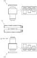
도 1은 본 발명의 일 실시예에 따른 디지털 현미경의 개략도.
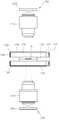
도 2는 본 발명의 일 실시예에 따른 디지털 현미경 중 스테이지를 확대한 도면.
도 3과 도 4는 본 발명의 일 실시예에 따른 디지털 현미경을 이용한 이미지 생성과정을 도시한 도면.
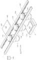
도 5는 본 발명의 일 실시예에 따른 디지털 현미경 중 고배율 촬상부의 사시도.
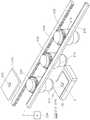
도 6은 본 발명의 일 실시예에 따른 디지털 현미경 중 고배율 촬상부의 작동상태도.1 is a schematic diagram of a digital microscope according to an embodiment of the present invention.
2 is an enlarged view of a stage in a digital microscope according to an embodiment of the present invention.
3 and 4 are diagrams showing an image generation process using a digital microscope according to an embodiment of the present invention.
5 is a perspective view of a high-magnification imaging unit in a digital microscope according to an embodiment of the present invention.
6 is an operational state diagram of a high-magnification imaging unit in a digital microscope according to an embodiment of the present invention.
첨부된 도면을 참조하여 본 발명에 따른 실시예를 상세히 설명한다. 이하, 본 발명에 따른 실시예를 설명함에 있어, 그리고 각 도면의 구성요소들에 참조부호를 부가함에 있어, 동일한 구성요소들에 대해서는 비록 다른 도면상에 표시되더라도 가능한 한 동일한 부호를 부가하였다.An embodiment according to the present invention will be described in detail with reference to the accompanying drawings. Hereinafter, in describing the embodiments according to the present invention, and in adding reference numerals to elements of each drawing, the same numerals are added to the same elements as possible even if they are indicated on different drawings.
본 발명은 일반인에서 전문가까지 여러 사람들이 범용적으로 사용할 수 있는 디지털 현미경에 관한 것으로, 사용자의 필요에 따라 고배율 이미지와 저배율 이미지를 선택적으로 생성할 수 있어 연구 개발 및 품질 관리 등을 위한 산업용으로 활용할 수 있을 뿐만 아니라 과학 교육 기자재로도 활용할 수 있는 디지털 현미경이다.The present invention relates to a digital microscope that can be used universally by various people from the general public to experts, and it is possible to selectively generate a high magnification image and a low magnification image according to the needs of the user, so it can be used for industrial purposes for research and development and quality control It is a digital microscope that not only can be used, but also can be used as a scientific educational equipment.
도 1을 참조하여 본 발명의 일 실시예에 따른 디지털 현미경에 대해 살펴보도록 한다.A digital microscope according to an embodiment of the present invention will be described with reference to FIG. 1.
본 실시예에 따른 디지털 현미경(10)은, 샘플(S)이 배치되는 스테이지(100)와, 스테이지(100)의 상부에 마련된 고배율 촬상부(200)와, 스테이지(100)의 하부에 마련된 저배율 촬상부(300)를 포함한다.The
도 2에 도시된 바와 같이, 스테이지(100)는, 샘플(S)이 안착되는 슬라이드(110)와, 슬라이드(110)에 안착된 샘플(S)에 빛을 조사하는 제1조광모듈(120) 및 제2조광모듈(130)로 구성된다.As shown in FIG. 2, the
슬라이드(110)는 측정 대상 샘플(S)을 고정하는 프레파라트(Preparat)의 일종으로서, 샘플(S)이 안착되는 슬라이드 글라스(112)와, 슬라이드 글라스(112)에 안착된 샘플(S)을 덮는 커버 글라스(114)로 이루어진다. 이때, 본 실시예의 슬라이드(110)는 통상의 프레파라트와 달리 슬라이드 글라스(112)와 커버 글라스(114)가 동일한 크기로 제작된다.The
제1조광모듈(120)은 슬라이드(110)의 상부에 구비되어 슬라이드(110)의 상부에서 하부로 빛을 조사함으로써 저배율 촬상부(300)를 통해 저배율 이미지가 생성되도록 한다.The
도면에 도시된 바와 같이, 제1조광모듈(120)은 제1광원(122), 제1확산렌즈(124) 및 제1도광판(126)으로 구성된다.As shown in the drawing, the
제1광원(122)은 슬라이드(110)의 샘플(S)에 빛을 조사하기 위한 발광수단으로서, 내구성이 우수하고 사용이 편리하며 다양한 색상을 방출할 수 있는 LED 광원일 수 있다.The
제1확산렌즈(124)는 제1광원(122)과 제1도광판(126)과 사이에 개재되어 제1광원(122)의 빛을 반복적으로 산란 또는/및 반사시킴으로써 제1도광판(126)의 상면과 하면에 핫 스팟이 나타나지 않도록 균일한 휘도의 빛을 출광시키는 역할을 한다.The
제1도광판(126)은 슬라이드(110)의 상부에 위치되어 제1도광판(126)의 일측에서 유입되는 제1광원(122)의 빛을 제1도광판(126)의 상면과 하면으로 출광시키는 면발광체이다.The first
제1도광판(126)의 상면에는 제1암막필름(128)이 부착되고, 제1도광판(126)의 타측면에는 제1반사시트(129)가 부착된다.The first
제1암막필름(128)은 전원 인가 시 투명하게 변하여 빛을 통과시키고 전원이 차단될 경우 불투명하게 변하여 빛을 반사시키는 PDLC(Polymer Dispersed Liquid Crystal) 필름이다.The first
또한, 제1반사시트(129)는 제1도광판(126)으로 유입된 제1광원(122)의 빛이 제1도광판(126)의 타측면으로 새는 것을 방지하기 위한 반사시트이다.In addition, the first
상술한 구성의 제1조광모듈(120)은, 제1광원(122)에 전원이 인가되어 점등될 경우 제1암막필름(128)에는 전원이 차단되어 불투명하게 변하게 된다. 따라서 제1광원(122)의 빛은 제1확산렌즈(124)를 거쳐 제1도광판(126)의 하면으로 출광된다.When the
제2조광모듈(130)은 슬라이드(110)의 하부에 구비되어 슬라이드(110)의 하부에서 상부로 빛을 조사함으로써 고배율 촬상부(200)를 통해 고배율 이미지가 생성되도록 한다.The
도면에 도시된 바와 같이, 제2조광모듈(130)은 제2광원(132), 제2확산렌즈(134) 및 제2도광판(136)으로 구성된다.As shown in the drawing, the
제2광원(132)은 슬라이드(110)의 샘플(S)에 빛을 조사하는 LED 광원이다.The
제2확산렌즈(134)는 제2광원(132)과 제2도광판(136)과 사이에 개재되어 제2광원(132)의 빛을 반복적으로 산란 또는/및 반사시킴으로써 균일한 휘도의 빛을 출광시킨다.The
제2도광판(136)은 슬라이드(110)의 하부에 위치되어 제2도광판(136)의 일측에서 유입되는 제2광원(132)의 빛을 제2도광판(136)의 상면과 하면으로 출광시키는 면발광체이다.The second
제2도광판(136)의 하면에는 PDLC 필름인 제2암막필름(128)이 부착되고, 제2도광판(136)의 타측면에는 빛샘을 방지하기 위한 제2반사시트(139)가 부착된다.A second
상술한 구성의 제2조광모듈(130)은, 제2광원(132)에 전원이 인가되어 점등될 경우 제2암막필름(138)에는 전원이 차단되어 불투명하게 변하게 된다. 따라서 제2광원(132)의 빛은 제2확산렌즈(134)를 거쳐 제2도광판(136)의 상면으로 출광된다.In the
도 3과 도 4을 참조하여 본 실시예에 따른 디지털 현미경(10)을 이용한 이미지 생성과정에 대해 설명하도록 한다.An image generation process using the
도 3에 도시된 바와 같이, 제2조광모듈(130)에 전원이 인가되면 제2광원(132)이 점등하여 빛을 발생시키고, 제2광원(132)에서 발생한 빛은 제2확산렌즈(134)를 통해 제2도광판(136)으로 유입된다. 이때, 제2암막필름(138)에는 전원이 인가되지 않으므로 제2광원(132)의 빛은 제2도광판(136)의 상면으로만 출광된다.As shown in FIG. 3, when power is applied to the
따라서, 제2조광모듈(130)의 빛이 스테이지(100)의 하부에서 상부로 조사되어 고배율 촬상부(200)를 통해 고배율 이미지를 생성할 수 있도록 한다.Accordingly, the light of the
한편, 제2조광모듈(130)에 전원이 인가될 경우 제1조광모듈(120)의 제1암막필름(128)에도 전원이 인가되는데, 이는 고배율 촬상부(200)가 투명해진 제1암막필름(128)을 통해 샘플(S)의 이미지를 촬영할 수 있도록 하기 위함이다.On the other hand, when power is applied to the
도 4에 도시된 바와 같이, 제1조광모듈(120)에 전원이 인가되면 제1광원(122)이 점등하여 빛을 발생시키고, 제1광원(122)에서 발생한 빛은 제1확산렌즈(124)를 통해 제1도광판(126)으로 유입된다. 이때, 제1암막필름(128)에는 전원이 인가되지 않으므로 제1광원(122)의 빛은 제1도광판(126)의 하면으로만 출광된다.As shown in FIG. 4, when power is applied to the
따라서, 제1조광모듈(120)의 빛이 스테이지(100)의 상부에서 하부로 조사되어 저배율 촬상부(300)를 통해 고배율 이미지를 생성할 수 있도록 한다.Accordingly, the light of the
한편, 제1조광모듈(120)에 전원이 인가될 경우 제2조광모듈(130)의 제2암막필름(138)에도 전원이 인가되는데, 이는 저배율 촬상부(300)가 투명해진 제2암막필름(138)을 통해 샘플(S)의 이미지를 촬영할 수 있도록 하기 위함이다.On the other hand, when power is applied to the
본 실시예에 따른 디지털 현미경(10)은 필요에 따라 여러 가지 배율의 렌즈를 교체하여 사용할 수 있도록 구성된다. 이를 위하여, 고배율 촬상부(200)와 저배율 촬상부(300)는 서로 다른 배율을 가진 렌즈를 2개 이상 포함하여 구성된다. 이때, 고배율 촬상부(200)와 저배율 촬상부(300)는 동일하게 구성되므로, 이하에서는 고배율 촬상부(200)를 일례로 그 구조를 살펴보도록 한다.The
도 5와 도 6에 도시된 바와 같이, 고배율 촬상부(200)는, 대물렌즈 어레이(210)와, 대물렌즈 어레이(210)의 렌즈(212,214,216)를 통해 확대된 샘플(S)의 이미지를 획득하는 이미지센서(220)와, 대물렌즈 어레이(210)의 렌즈(212,214,216)를 이미지센서(220) 측으로 이동시키는 구동수단(230)과, 이미지센서(220) 측으로 이동한 렌즈(212,214,216)와의 동축도를 감지하기 위한 어레이 센서(240)로 구성된다.5 and 6, the high
대물렌즈 어레이(210)는 사용자의 필요에 따라 여러 가지 배율의 이미지를 생성할 수 있도록 서로 다른 배율을 가진 2개 이상(본 실시예에서는 3개)의 렌즈(212,214,216)로 구성된다.The
이미지센서(220)는 대물렌즈 어레이(210)에서 선택된 하나의 렌즈(212,214,216)를 통해 확대된 샘플(S)의 이미지를 생성하는 센서로서, CCD(Change Coupled Deivce)센서 또는 COMS(Complementary Metal Oxide Semiconductor)센서일 수 있다.The
구동수단(230)은, 대물렌즈 어레이(210)의 렌즈(212,214,216)에 마련된 피니언 기어(232)와, 피니언 기어(232)에 맞물리는 고정 랙기어(234)와, 고정 랙기어(234)와 대향하게 위치되고 피니언 기어(232)에 맞물리는 가동 랙기어(236)와, 가동 랙기어(236)를 이동시키는 액추에이터(238)로 구성된다.The driving means 230 includes a
상술한 구성의 구동수단(230)은 액추에이터(238)가 작동할 경우 가동 랙기어(236)가 길이 방향으로 이동하며 대물렌즈 어레이(210)의 렌즈(212,214,216)를 이미지센서(220) 측으로 이동시킨다.When the
이때, 액추에이터(238)는 렌즈(212,214,216)의 이동을 정밀하게 제어할 수 있는 스태핑 모터인 것이 바람직하다.In this case, the
어레이 센서(240)는 구동수단(230)에 의해 이동한 렌즈(212,214,216)와 이미지 센서(220)의 동축도를 감지하기 위한 수단으로, 어레이 센서(240)에서 측정된 값에 의해 액추에이터(238)의 작동이 제어된다.The
전술한 바와 같이, 저배율 촬상부(300)는 고배율 촬상부(200)와 동일한 구성 및 작동원리를 가지므로 이에 대한 상세한 설명을 생략하기로 한다.As described above, since the low
이상 본 발명을 바람직한 실시예를 통하여 설명하였는데, 상술한 실시예는 본 발명의 기술적 사상을 예시적으로 설명한 것에 불과하며, 본 발명의 기술적 사상을 벗어나지 않는 범위 내에서 다양한 변화가 가능함은 이 분야에서 통상의 지식을 가진 자라면 이해할 수 있을 것이다. 따라서 본 발명의 보호범위는 특정 실시예가 아니라 특허청구범위에 기재된 사항에 의해 해석되어야 하며, 그와 동등한 범위 내에 있는 모든 기술적 사상도 본 발명의 권리범위에 포함되는 것으로 해석되어야 할 것이다.The present invention has been described above through preferred embodiments, but the above-described embodiments are merely illustrative of the technical idea of the present invention, and various changes are possible within the scope not departing from the technical idea of the present invention. Those of ordinary skill will understand. Accordingly, the scope of protection of the present invention should be interpreted not by specific embodiments, but by the matters described in the claims, and all technical ideas within the scope equivalent thereto should be interpreted as being included in the scope of the present invention.
10: 디지털 현미경100: 스테이지
200: 고배율 촬상부300: 저배율 촬상부10: digital microscope 100: stage
200: high magnification imaging unit 300: low magnification imaging unit
Claims (13)
Translated fromKorean상기 스테이지의 상부에 마련된 고배율 촬상부; 및
상기 스테이지의 하부에 마련된 저배율 촬상부를 포함하고,
상기 스테이지는, 샘플이 안착되는 슬라이드와, 상기 슬라이드의 상부에 구비된 제1조광모듈과, 상기 슬라이드의 하부에 구비된 제2조광모듈로 구성되며,
상기 제1조광모듈은, 상기 슬라이드의 상부에 구비된 제1도광판과, 상기 제1도광판의 일측에 마련된 제1광원과, 상기 제1도광판의 상면에 부착되어 전원 인가 시 투명하게 변하는 제1암막필름으로 구성되고,
상기 제2조광모듈은, 상기 슬라이드의 하부에 구비된 제2도광판과, 상기 제2도광판의 일측에 마련된 제2광원과, 상기 제2도광판의 하면에 부착되어 전원 인가 시 투명하게 변하는 제2암막필름으로 구성되며,
상기 제1조광모듈에 전원이 인가되면 상기 슬라이드의 상부에서 하부로 빛이 조사되어 상기 저배율 촬상부를 통해 이미지를 생성하고, 상기 제2조광모듈에 전원이 인가되면 상기 슬라이드의 하부에서 상부로 빛이 조사되어 상기 고배율 촬상부를 통해 이미지를 생성하는 것을 특징으로 하는 디지털 현미경.
A stage on which a sample is placed;
A high magnification imaging unit provided on the upper part of the stage; And
Including a low magnification imaging unit provided in the lower portion of the stage,
The stage is composed of a slide on which a sample is mounted, a first dimming module provided on an upper portion of the slide, and a second dimming module provided on a lower portion of the slide,
The first light guide module includes a first light guide plate provided on an upper portion of the slide, a first light source provided on one side of the first light guide plate, and a first black film attached to an upper surface of the first light guide plate to become transparent when power is applied. Consists of a film,
The second light guide module includes a second light guide plate provided under the slide, a second light source provided on one side of the second light guide plate, and a second dark film attached to a lower surface of the second light guide plate and becomes transparent when power is applied. Consists of a film,
When power is applied to the first dimming module, light is irradiated from the top to the bottom of the slide to generate an image through the low magnification imaging unit, and when power is applied to the second dimming module, light is emitted from the bottom of the slide to the top. A digital microscope, characterized in that it is irradiated to generate an image through the high-magnification imaging unit.
상기 제1암막필름과 상기 제2암막필름은 PDLC(Polymer Dispersed Liquid Crystal) 필름인 것을 특징으로 하는 디지털 현미경.
The method according to claim 1,
The first black film and the second black film are a digital microscope, characterized in that the PDLC (Polymer Dispersed Liquid Crystal) film.
상기 제1도광판과 상기 제1광원 사이에는 제1확산렌즈가 구비되고, 상기 제2도광판과 상기 제2광원 사이에는 제2확산렌즈가 구비되는 것을 특징으로 하는 디지털 현미경.
The method of claim 3,
A digital microscope, wherein a first diffusion lens is provided between the first light guide plate and the first light source, and a second diffusion lens is provided between the second light guide plate and the second light source.
상기 제1도광판의 타측에는 제1반사시트가 부착되고, 상기 제2도광판의 타측에는 제2반사시트가 부착되는 것을 특징으로 하는 디지털 현미경.
The method of claim 4,
A digital microscope, characterized in that a first reflective sheet is attached to the other side of the first light guide plate, and a second reflective sheet is attached to the other side of the second light guide plate.
상기 고배율 촬상부는,
서로 다른 배율을 가진 2개 이상의 렌즈로 구성된 대물렌즈 어레이와,
상기 대물렌즈 어레이에서 선택된 하나의 렌즈를 통해 확대된 샘플의 이미지를 획득하는 이미지센서와,
상기 대물렌즈 어레이에서 선택된 하나의 렌즈를 상기 이미지센서 측으로 이동시키는 구동수단으로 구성되는 것을 특징으로 하는 디지털 현미경.
The method according to any one of claims 1 and 3 to 5,
The high magnification imaging unit,
An objective lens array consisting of two or more lenses with different magnifications,
An image sensor that acquires an image of a sample magnified through one lens selected from the objective lens array,
And a driving means for moving one lens selected from the objective lens array toward the image sensor.
상기 구동수단은, 상기 대물렌즈 어레이의 각 렌즈에 마련된 피니언 기어와, 상기 피니언 기어에 맞물리는 고정 랙기어와, 상기 고정 랙기어와 대향하게 위치되고 상기 피니언 기어에 맞물리는 가동 랙기어와, 상기 가동 랙기어를 이동시키는 액추에이터로 구성된 것을 특징으로 하는 디지털 현미경.
The method of claim 6,
The driving means includes a pinion gear provided on each lens of the objective lens array, a fixed rack gear meshing with the pinion gear, a movable rack gear positioned opposite the fixed rack gear and meshing with the pinion gear, and the Digital microscope, characterized in that consisting of an actuator that moves the movable rack gear.
상기 구동수단은 상기 이미지센서 측으로 이동한 렌즈와의 동축도를 감지하기 위한 어레이 센서를 더 포함하여 구성되는 것을 특징으로 하는 디지털 현미경.
The method of claim 7,
The driving means further comprises an array sensor for detecting a degree of coaxiality with the lens moved toward the image sensor.
상기 액추에이터는 스태핑 모터인 것을 특징으로 하는 디지털 현미경.
The method of claim 8,
The actuator is a digital microscope, characterized in that the stepping motor.
상기 저배율 촬상부는,
서로 다른 배율을 가진 2개 이상의 렌즈로 구성된 대물렌즈 어레이와,
상기 대물렌즈 어레이에서 선택된 하나의 렌즈를 통해 확대된 샘플의 이미지를 획득하는 이미지센서와,
상기 대물렌즈 어레이에서 선택된 하나의 렌즈를 상기 이미지센서 측으로 이동시키는 구동수단으로 구성되는 것을 특징으로 하는 디지털 현미경.
The method according to any one of claims 1 and 3 to 5,
The low magnification imaging unit,
An objective lens array consisting of two or more lenses with different magnifications,
An image sensor that acquires an image of a sample magnified through one lens selected from the objective lens array,
And a driving means for moving one lens selected from the objective lens array toward the image sensor.
상기 구동수단은, 상기 대물렌즈 어레이의 각 렌즈에 마련된 피니언 기어와, 상기 피니언 기어에 맞물리는 고정 랙기어와, 상기 고정 랙기어와 대향하게 위치되고 상기 피니언 기어에 맞물리는 가동 랙기어와, 상기 가동 랙기어를 이동시키는 액추에이터로 구성된 것을 특징으로 하는 디지털 현미경.
The method of claim 10,
The driving means includes a pinion gear provided on each lens of the objective lens array, a fixed rack gear meshing with the pinion gear, a movable rack gear positioned opposite the fixed rack gear and meshing with the pinion gear, and the Digital microscope, characterized in that consisting of an actuator that moves the movable rack gear.
상기 구동수단은 상기 이미지센서 측으로 이동한 렌즈와의 동축도를 감지하기 위한 어레이 센서를 더 포함하여 구성되는 것을 특징으로 하는 디지털 현미경.
The method of claim 11,
The driving means further comprises an array sensor for detecting a degree of coaxiality with the lens moved toward the image sensor.
상기 액추에이터는 스태핑 모터인 것을 특징으로 하는 디지털 현미경.The method of claim 12,
The actuator is a digital microscope, characterized in that the stepping motor.
Priority Applications (1)
| Application Number | Priority Date | Filing Date | Title |
|---|---|---|---|
| KR1020200158448AKR102223433B1 (en) | 2020-11-24 | 2020-11-24 | Digital microscope |
Applications Claiming Priority (1)
| Application Number | Priority Date | Filing Date | Title |
|---|---|---|---|
| KR1020200158448AKR102223433B1 (en) | 2020-11-24 | 2020-11-24 | Digital microscope |
Publications (1)
| Publication Number | Publication Date |
|---|---|
| KR102223433B1true KR102223433B1 (en) | 2021-03-05 |
Family
ID=75163992
Family Applications (1)
| Application Number | Title | Priority Date | Filing Date |
|---|---|---|---|
| KR1020200158448AActiveKR102223433B1 (en) | 2020-11-24 | 2020-11-24 | Digital microscope |
Country Status (1)
| Country | Link |
|---|---|
| KR (1) | KR102223433B1 (en) |
Citations (10)
| Publication number | Priority date | Publication date | Assignee | Title |
|---|---|---|---|---|
| JPH07218842A (en)* | 1994-02-09 | 1995-08-18 | Dainippon Printing Co Ltd | Microscope image input / output system |
| KR200294068Y1 (en)* | 2002-06-03 | 2002-11-04 | (주)시원광기술 | Digital Microscope |
| CN102472888A (en)* | 2009-07-06 | 2012-05-23 | 株式会社尼康 | Microscope |
| JP2016102854A (en)* | 2014-11-27 | 2016-06-02 | オリンパス株式会社 | Microscope system |
| KR101741686B1 (en)* | 2015-12-30 | 2017-05-31 | 신진엠텍(주) | Optical structure and method for method for optical structure |
| KR20170127972A (en)* | 2016-05-13 | 2017-11-22 | 주식회사 고영테크놀러지 | Biological Tissue Inspection Apparatus and Method thereof |
| JP2018014377A (en)* | 2016-07-20 | 2018-01-25 | 東レエンジニアリング株式会社 | Defect inspection device of wide gap semiconductor substrate |
| KR20190098326A (en)* | 2018-02-14 | 2019-08-22 | 주식회사 리암솔루션 | Probe station for measuring L-I-V |
| KR20200052157A (en)* | 2018-11-06 | 2020-05-14 | (주) 솔 | Digital microscope in which high-magnification image is guided by low-magnification image and digital microscope system |
| CN211478754U (en)* | 2020-03-20 | 2020-09-11 | 桂林市迈特光学仪器有限公司 | Shadowless LED microscope base light source |
- 2020
- 2020-11-24KRKR1020200158448Apatent/KR102223433B1/enactiveActive
Patent Citations (10)
| Publication number | Priority date | Publication date | Assignee | Title |
|---|---|---|---|---|
| JPH07218842A (en)* | 1994-02-09 | 1995-08-18 | Dainippon Printing Co Ltd | Microscope image input / output system |
| KR200294068Y1 (en)* | 2002-06-03 | 2002-11-04 | (주)시원광기술 | Digital Microscope |
| CN102472888A (en)* | 2009-07-06 | 2012-05-23 | 株式会社尼康 | Microscope |
| JP2016102854A (en)* | 2014-11-27 | 2016-06-02 | オリンパス株式会社 | Microscope system |
| KR101741686B1 (en)* | 2015-12-30 | 2017-05-31 | 신진엠텍(주) | Optical structure and method for method for optical structure |
| KR20170127972A (en)* | 2016-05-13 | 2017-11-22 | 주식회사 고영테크놀러지 | Biological Tissue Inspection Apparatus and Method thereof |
| JP2018014377A (en)* | 2016-07-20 | 2018-01-25 | 東レエンジニアリング株式会社 | Defect inspection device of wide gap semiconductor substrate |
| KR20190098326A (en)* | 2018-02-14 | 2019-08-22 | 주식회사 리암솔루션 | Probe station for measuring L-I-V |
| KR20200052157A (en)* | 2018-11-06 | 2020-05-14 | (주) 솔 | Digital microscope in which high-magnification image is guided by low-magnification image and digital microscope system |
| CN211478754U (en)* | 2020-03-20 | 2020-09-11 | 桂林市迈特光学仪器有限公司 | Shadowless LED microscope base light source |
Similar Documents
| Publication | Publication Date | Title |
|---|---|---|
| JP6012184B2 (en) | Microscope transmitted illumination device | |
| US7554727B2 (en) | Illumination apparatus for microscope | |
| CN105158888B (en) | Programmable microscope condenser lens device and imaging method based on LCD liquid crystal panel | |
| JPWO2018061883A1 (en) | Observation device | |
| JPWO2018220670A1 (en) | Observation device | |
| DE102006035179B4 (en) | Coordinate measuring machine with a lighting device for illuminating an object | |
| JPH11133308A (en) | Transmitted illumination device for microscope | |
| KR102223433B1 (en) | Digital microscope | |
| JP2007078581A (en) | Illumination device for visual inspection | |
| WO2018087665A1 (en) | Portable upright bright field microscope with smart device compatibility | |
| JP2009109566A (en) | Subject holding stage and observing device | |
| CN109960026B (en) | Illumination device, microscope device, and cassette | |
| JP2007033381A (en) | Optical inspection apparatus and its lighting method | |
| US12235427B2 (en) | Observation apparatus | |
| CN105869491B (en) | A kind of device of transmission electron microscope teaching mode | |
| JP2007219121A (en) | Microscope visual field light distribution measurement device | |
| JP2013142774A (en) | Illumination device and magnifying observation device | |
| JP5849540B2 (en) | Microscope illumination device and microscope | |
| JPH11287958A (en) | CCD microscope and illumination device used for it | |
| DE102006016358A1 (en) | Microscope includes at least two chambers for protective, sealed fitting of mechanical, optical and electronic component groups in different chambers, for protection against dust, humidity and similar contaminants | |
| GB2029045A (en) | Viewing an image of a writing bema | |
| JP2007017901A (en) | Illumination device and microscope | |
| JP4307944B2 (en) | Shutter device, laser scanning microscope and microscope | |
| CN209928132U (en) | Projection microscope | |
| JP2006337925A (en) | Lighting device of microscope |
Legal Events
| Date | Code | Title | Description |
|---|---|---|---|
| PA0109 | Patent application | Patent event code:PA01091R01D Comment text:Patent Application Patent event date:20201124 | |
| PA0201 | Request for examination | ||
| PA0302 | Request for accelerated examination | Patent event date:20201124 Patent event code:PA03022R01D Comment text:Request for Accelerated Examination | |
| E902 | Notification of reason for refusal | ||
| PE0902 | Notice of grounds for rejection | Comment text:Notification of reason for refusal Patent event date:20210121 Patent event code:PE09021S01D | |
| E701 | Decision to grant or registration of patent right | ||
| PE0701 | Decision of registration | Patent event code:PE07011S01D Comment text:Decision to Grant Registration Patent event date:20210223 | |
| GRNT | Written decision to grant | ||
| PR0701 | Registration of establishment | Comment text:Registration of Establishment Patent event date:20210226 Patent event code:PR07011E01D | |
| PR1002 | Payment of registration fee | Payment date:20210226 End annual number:3 Start annual number:1 | |
| PG1601 | Publication of registration | ||
| PR1001 | Payment of annual fee | Payment date:20231207 Start annual number:4 End annual number:4 | |
| PR1001 | Payment of annual fee | Payment date:20250211 Start annual number:5 End annual number:5 |