KR102218757B1 - Manufacturing Method of Double Tube for Semiconductor Process - Google Patents
Manufacturing Method of Double Tube for Semiconductor ProcessDownload PDFInfo
- Publication number
- KR102218757B1 KR102218757B1KR1020190165194AKR20190165194AKR102218757B1KR 102218757 B1KR102218757 B1KR 102218757B1KR 1020190165194 AKR1020190165194 AKR 1020190165194AKR 20190165194 AKR20190165194 AKR 20190165194AKR 102218757 B1KR102218757 B1KR 102218757B1
- Authority
- KR
- South Korea
- Prior art keywords
- pipe
- resin
- steel pipe
- manufacturing
- tube
- Prior art date
- Legal status (The legal status is an assumption and is not a legal conclusion. Google has not performed a legal analysis and makes no representation as to the accuracy of the status listed.)
- Active
Links
Images


Classifications
- B—PERFORMING OPERATIONS; TRANSPORTING
- B29—WORKING OF PLASTICS; WORKING OF SUBSTANCES IN A PLASTIC STATE IN GENERAL
- B29C—SHAPING OR JOINING OF PLASTICS; SHAPING OF MATERIAL IN A PLASTIC STATE, NOT OTHERWISE PROVIDED FOR; AFTER-TREATMENT OF THE SHAPED PRODUCTS, e.g. REPAIRING
- B29C65/00—Joining or sealing of preformed parts, e.g. welding of plastics materials; Apparatus therefor
- B29C65/02—Joining or sealing of preformed parts, e.g. welding of plastics materials; Apparatus therefor by heating, with or without pressure
- B29C65/08—Joining or sealing of preformed parts, e.g. welding of plastics materials; Apparatus therefor by heating, with or without pressure using ultrasonic vibrations
- B—PERFORMING OPERATIONS; TRANSPORTING
- B29—WORKING OF PLASTICS; WORKING OF SUBSTANCES IN A PLASTIC STATE IN GENERAL
- B29C—SHAPING OR JOINING OF PLASTICS; SHAPING OF MATERIAL IN A PLASTIC STATE, NOT OTHERWISE PROVIDED FOR; AFTER-TREATMENT OF THE SHAPED PRODUCTS, e.g. REPAIRING
- B29C65/00—Joining or sealing of preformed parts, e.g. welding of plastics materials; Apparatus therefor
- B29C65/48—Joining or sealing of preformed parts, e.g. welding of plastics materials; Apparatus therefor using adhesives, i.e. using supplementary joining material; solvent bonding
- B—PERFORMING OPERATIONS; TRANSPORTING
- B29—WORKING OF PLASTICS; WORKING OF SUBSTANCES IN A PLASTIC STATE IN GENERAL
- B29C—SHAPING OR JOINING OF PLASTICS; SHAPING OF MATERIAL IN A PLASTIC STATE, NOT OTHERWISE PROVIDED FOR; AFTER-TREATMENT OF THE SHAPED PRODUCTS, e.g. REPAIRING
- B29C66/00—General aspects of processes or apparatus for joining preformed parts
- B29C66/50—General aspects of joining tubular articles; General aspects of joining long products, i.e. bars or profiled elements; General aspects of joining single elements to tubular articles, hollow articles or bars; General aspects of joining several hollow-preforms to form hollow or tubular articles
- B29C66/51—Joining tubular articles, profiled elements or bars; Joining single elements to tubular articles, hollow articles or bars; Joining several hollow-preforms to form hollow or tubular articles
- B29C66/52—Joining tubular articles, bars or profiled elements
- B29C66/522—Joining tubular articles
- B29C66/5227—Joining tubular articles for forming multi-tubular articles by longitudinally joining elementary tubular articles wall-to-wall (e.g. joining the wall of a first tubular article to the wall of a second tubular article) or for forming multilayer tubular articles
- B29C66/52271—Joining tubular articles for forming multi-tubular articles by longitudinally joining elementary tubular articles wall-to-wall (e.g. joining the wall of a first tubular article to the wall of a second tubular article) or for forming multilayer tubular articles one tubular article being placed inside the other
- C—CHEMISTRY; METALLURGY
- C08—ORGANIC MACROMOLECULAR COMPOUNDS; THEIR PREPARATION OR CHEMICAL WORKING-UP; COMPOSITIONS BASED THEREON
- C08L—COMPOSITIONS OF MACROMOLECULAR COMPOUNDS
- C08L27/00—Compositions of homopolymers or copolymers of compounds having one or more unsaturated aliphatic radicals, each having only one carbon-to-carbon double bond, and at least one being terminated by a halogen; Compositions of derivatives of such polymers
- C08L27/02—Compositions of homopolymers or copolymers of compounds having one or more unsaturated aliphatic radicals, each having only one carbon-to-carbon double bond, and at least one being terminated by a halogen; Compositions of derivatives of such polymers not modified by chemical after-treatment
- C08L27/12—Compositions of homopolymers or copolymers of compounds having one or more unsaturated aliphatic radicals, each having only one carbon-to-carbon double bond, and at least one being terminated by a halogen; Compositions of derivatives of such polymers not modified by chemical after-treatment containing fluorine atoms
- B—PERFORMING OPERATIONS; TRANSPORTING
- B29—WORKING OF PLASTICS; WORKING OF SUBSTANCES IN A PLASTIC STATE IN GENERAL
- B29K—INDEXING SCHEME ASSOCIATED WITH SUBCLASSES B29B, B29C OR B29D, RELATING TO MOULDING MATERIALS OR TO MATERIALS FOR MOULDS, REINFORCEMENTS, FILLERS OR PREFORMED PARTS, e.g. INSERTS
- B29K2101/00—Use of unspecified macromolecular compounds as moulding material
- B29K2101/12—Thermoplastic materials
- B—PERFORMING OPERATIONS; TRANSPORTING
- B29—WORKING OF PLASTICS; WORKING OF SUBSTANCES IN A PLASTIC STATE IN GENERAL
- B29L—INDEXING SCHEME ASSOCIATED WITH SUBCLASS B29C, RELATING TO PARTICULAR ARTICLES
- B29L2023/00—Tubular articles
- B29L2023/22—Tubes or pipes, i.e. rigid
Landscapes
- Engineering & Computer Science (AREA)
- Mechanical Engineering (AREA)
- Chemical & Material Sciences (AREA)
- Health & Medical Sciences (AREA)
- Chemical Kinetics & Catalysis (AREA)
- Medicinal Chemistry (AREA)
- Polymers & Plastics (AREA)
- Organic Chemistry (AREA)
- Lining Or Joining Of Plastics Or The Like (AREA)
- Light Receiving Elements (AREA)
- Rigid Pipes And Flexible Pipes (AREA)
Abstract
Description
Translated fromKorean본 발명(Disclosure)은, 반도체 공정용 이중관 제조방법에 관한 것으로서, 구체적으로, 이중관의 내측에 배치되는 수지관을 몰딩 성형방법으로 성형한 후 강관에 삽입후 접착함으로써, 우수한 품질의 이중관을 낮은 제조비용으로 제조할 수 있는 반도체 공정용 이중관 제조방법에 관한 것이다.The present invention (Disclosure) relates to a method of manufacturing a double pipe for a semiconductor process, and specifically, a resin pipe disposed inside the double pipe is molded by a molding method, inserted into a steel pipe, and then bonded, thereby manufacturing a double pipe of excellent quality. It relates to a method for manufacturing a double tube for a semiconductor process that can be manufactured at cost.
여기서는, 본 발명에 관한 배경기술이 제공되며, 이들이 반드시 공지기술을 의미하는 것은 아니다(This section provides background information related to the present disclosure which is not necessarily prior art).Here, background technology related to the present invention is provided, and these do not necessarily mean known technology (This section provides background information related to the present disclosure which is not necessarily prior art).
반도체 공정용 이중관은, 다양한 종류의 독성 물질 또는 유해물질들을 포함하는 액상 또는 기상 형태의 화학 물질들이 유동하며 이송된다.In the double tube for semiconductor processing, liquid or gaseous chemical substances including various kinds of toxic substances or harmful substances are transported while flowing.
이중관을 이루는 수지관과 강관은 그 재질이 상이한데, 일반적으로 강관은 이중관 자체의 강성을 유지하기 위하여 스테인레스 강을 사용한다. 이에 반해서, 수지관은 화학적 반응성이 낮으며 물리적으로 안정적인 물질을 그 재질로 한다.Resin pipes and steel pipes constituting a double pipe have different materials, and generally, stainless steel is used to maintain the rigidity of the double pipe itself. In contrast, the resin tube is made of a material that has low chemical reactivity and is physically stable.
수지관의 내면은 상술한 화학 물질들이 직접 접촉하기 때문에, 기밀성을 유지하는 것이 무엇보다 중요하다. Since the above-described chemical substances directly contact the inner surface of the resin tube, it is most important to maintain airtightness.
수지관에 작은 균열이나 파손이 발생해도, 금속성의 강관을 파손할 수 있는 치명적인 화학작용이 발생할 수 있다.Even if a small crack or breakage occurs in the resin pipe, a fatal chemical reaction may occur that can damage the metallic steel pipe.
반도체 공정용 이중관을 제조하는 종래의 방법에서는, 완성된 강관의 내면에 다양한 방법으로 이중관을 형성한다.In the conventional method of manufacturing a double pipe for a semiconductor process, a double pipe is formed on the inner surface of the finished steel pipe by various methods.
우선, 수지관의 재료가 되는 각종 수지류를 액상 상태로 분사하여 코팅하는 코팅공법이 있다. 이 방법은 200㎛ 내외의 얇은 막을 여러차례 코팅함으로써, 수지관을 형성한다. First, there is a coating method in which various resins, which are materials for resin pipes, are sprayed in a liquid state and coated. In this method, a resin tube is formed by coating a thin film of about 200 mu m several times.
다음으로 라이닝 공법을 이용하여 강관의 내면에 2mm 내외의 두꺼운 막층을 형성한다. 대표적인 라이닝 공법으로는 Lot 라이닝 공법이 있다.Next, a thick film layer of about 2 mm is formed on the inner surface of the steel pipe using the lining method. As a typical lining method, there is a lot lining method.
다음으로 강관의 내면에 수지관의 재료가 되는 액상의 레진을 직접 사출하여 수지관을 형성하는 직접 사출공법이 있다.Next, there is a direct injection method in which a resin tube is formed by directly injecting liquid resin, which is a material of the resin tube, onto the inner surface of the steel tube.
상술한 종래의 이중관 제조방법은, 완성된 강관의 내면에 직접 수지관을 형성하는 방법으로서, 수지관과 강관 사이의 높은 밀착성을 쉽게 구현할 수 있고, 수지관의 성형 과정이 불필요하다는 장점이 있다.The above-described conventional method for manufacturing a double pipe is a method of directly forming a resin pipe on the inner surface of a finished steel pipe, and has an advantage that high adhesion between the resin pipe and the steel pipe can be easily implemented, and a molding process of the resin pipe is unnecessary.
그러나, 코팅이나 라이닝 공법으로 형성된 수지관은 형성 과정에서 버블(bubble) 또는 크랙(crack)이 형성되어, 내구성이 약한 문제점이 있다.However, a resin tube formed by a coating or lining method has a problem of poor durability because bubbles or cracks are formed during the formation process.
또한 작업성이 현저히 떨어지고, 이에 따라 상술한 바와 같은 수지관의 내구성이 떨어지는 문제가 동반될 수도 있다.In addition, workability is remarkably deteriorated, and thus, a problem of deteriorating durability of the resin tube as described above may be accompanied.
또한, 자동화 장비 또는 공정을 적용하기 어렵기 때문에, 제조비용이 상승하여 경제성이 떨어지는 문제점도 있다.In addition, since it is difficult to apply an automated equipment or process, there is a problem in that the manufacturing cost is increased and thus economical efficiency is decreased.
직접 사출공법은 직경이 큰 이중관을 제조할때, 금형의 크기가 대형화되는 문제점을 가진다.The direct injection method has a problem in that the size of the mold becomes large when manufacturing a double tube with a large diameter.
본 발명(Disclosure)은, 내구성과 작업성이 향상되고 경제성이 우수한 반도체 공정용 이중관 제조방법의 제공을 일 목적으로 한다.An object of the present invention (Disclosure) is to provide a method for manufacturing a double pipe for semiconductor processing, which has improved durability and workability and excellent economical efficiency.
여기서는, 본 발명의 전체적인 요약(Summary)이 제공되며, 이것이 본 발명의 외연을 제한하는 것으로 이해되어서는 아니 된다(This section provides a general summary of the disclosure and is not a comprehensive disclosure of its full scope or all of its features).Here, a summary of the present invention is provided, and this section provides a general summary of the disclosure and is not a comprehensive disclosure of its full scope or all of its features).
상기한 과제의 해결을 위해, 본 발명을 기술하는 여러 관점들 중 어느 일 관점(aspect)에 따른 반도체 공정용 이중관 제조방법은, 강관와 상기 강관의 내면에 융착되는 수지관으로 형성되는 반도체 공정용 이중관 제조방법으로서, 상기 강관을 가공하여 준비하고, 탄성변형 및 복원이 가능한 재질로 구비되는 상기 수지관을 금형을 이용한 성형방법으로 성형하여 준비하는 제1 단계; 상기 수지관은 탄성변형시켜 상기 강관의 내측에 삽입시킨 후, 상기 수지관의 탄성복원력에 의해 상기 수지관의 외면이 상기 강관의 내면에 밀착되게 위치시키는 제2 단계; 및 상기 수지관의 외면과 상기 강관의 내면을 접합하는 제3 단계;를 포함한다.In order to solve the above problems, a method for manufacturing a double pipe for a semiconductor process according to any one of the various aspects describing the present invention includes a double pipe for a semiconductor process formed of a steel pipe and a resin tube fused to the inner surface of the steel pipe. A manufacturing method, comprising: a first step of preparing the steel pipe by processing and preparing the resin pipe formed of a material capable of elastic deformation and restoration by molding by a molding method using a mold; A second step of elastically deforming the resin pipe and inserting it into the inside of the steel pipe, and then positioning the outer surface of the resin pipe to be in close contact with the inner surface of the steel pipe by the elastic restoring force of the resin pipe; And a third step of bonding the outer surface of the resin pipe and the inner surface of the steel pipe.
본 발명을 기술하는 여러 관점들 중 어느 일 관점(aspect)에 따른 반도체 공정용 이중관 제조방법에서, 상기 제2 단계는, 상기 수지관의 외면에 상기 강관의 내면과 접합성을 향상시키는 접착층을 더 형성하는 것을 특징으로 한다. In the method for manufacturing a double pipe for a semiconductor process according to any one of the various aspects describing the present invention, the second step is to further form an adhesive layer on the outer surface of the resin pipe to improve the adhesion with the inner surface of the steel pipe Characterized in that.
본 발명을 기술하는 여러 관점들 중 어느 일 관점(aspect)에 따른 반도체 공정용 이중관 제조방법에서, 상기 수지관은, 탄성변형이 가능한 열가소성 수지 재질로 구비되는 것을 특징으로 한다. In the method for manufacturing a double pipe for a semiconductor process according to any one aspect of the various aspects describing the present invention, the resin pipe is characterized in that it is provided with a thermoplastic resin material capable of elastic deformation.
본 발명을 기술하는 여러 관점들 중 어느 일 관점(aspect)에 따른 반도체 공정용 이중관 제조방법에서, 상기 수지관은, PTFE(Polytetrafluoroethylene), PFA(Perfluoroalkoxy), FEP(Fluorinated Ethylene Propylene), ETFE(Ethylene tetrafluoroethylene), ECTFE(ethylene chlorotrifluoroethylene), PVDF(polyvinylidene fluoride) 중에서 선택된 불소계열 수지로 구비되는 것을 특징으로 한다.In the method for manufacturing a double tube for a semiconductor process according to any one of the various aspects describing the present invention, the resin tube includes polytetrafluoroethylene (PTFE), perfluoroalkoxy (PFA), Fluorinated Ethylene Propylene (FEP), and Ethylene (ETFE). It is characterized in that it is provided with a fluorine-based resin selected from tetrafluoroethylene), ethylene chlorotrifluoroethylene (ECTFE), and polyvinylidene fluoride (PVDF).
본 발명을 기술하는 여러 관점들 중 어느 일 관점(aspect)에 따른 반도체 공정용 이중관 제조방법에서, 상기 제3 단계는, 상기 수지층과 상기 강관의 계면에 초음파를 인가하여 상기 수지관과 상기 강관을 접합하는 초음파 융착 수단을 이용하는 것을 특징으로 한다.In the method for manufacturing a double pipe for a semiconductor process according to any one of the various aspects describing the present invention, the third step is to apply ultrasonic waves to the interface between the resin layer and the steel pipe to provide the resin pipe and the steel pipe. It characterized in that it uses an ultrasonic welding means for bonding.
본 발명을 기술하는 여러 관점들 중 어느 일 관점(aspect)에 따른 반도체 공정용 이중관 제조방법에서, 상기 초음파 융착 수단은, 집속 초음파(focused ultrasound)를 이용하는 것을 특징으로 한다.In the method for manufacturing a double tube for a semiconductor process according to any one of the various aspects describing the present invention, the ultrasonic welding means is characterized by using focused ultrasound.
본 발명을 기술하는 여러 관점들 중 어느 일 관점(aspect)에 따른 반도체 공정용 이중관 제조방법에서, 상기 초음파 융착 수단은, 전력을 공급하는 전원부; 상기 전력을 이용하여 고주파 신호를 생성하는 고주파 생성부; 상기 고주파 신호를 이용하여 초음파를 생성하는 초음파 생성부; 및 상기 초음파를 집속하여 상기 접착층에 고강도 집속 초음파를 인가하는 초음파 집속부;를 포함하는 것을 특징으로 한다.In the method for manufacturing a double tube for a semiconductor process according to any one of the various aspects describing the present invention, the ultrasonic welding means comprises: a power supply unit for supplying power; A high frequency generator generating a high frequency signal using the power; An ultrasonic generator for generating ultrasonic waves by using the high-frequency signal; And an ultrasonic focusing unit that focuses the ultrasonic waves and applies high-intensity focused ultrasonic waves to the adhesive layer.
본 발명을 기술하는 여러 관점들 중 어느 일 관점(aspect)에 따른 반도체 공정용 이중관 제조방법에서, 상기 초음파 생성부는 적어도 두 개 이상으로 구성되고, 각각의 상기 초음파 생성부에서 생성되는 초음파의 전파(propagation) 방향을 제어하는 정렬부를 더 포함하는 것을 특징으로 한다.In the method of manufacturing a double tube for a semiconductor process according to any one of the various aspects describing the present invention, the ultrasonic generator is composed of at least two or more, and the propagation of ultrasonic waves generated by each of the ultrasonic generators ( It characterized in that it further comprises an alignment unit for controlling the direction of propagation.
본 발명에 따르면, 반도체 공정용 폐가스에 대한 내식성이 우수한 수지재질의 수지관과, 외부 충격에 안정적인 강관을 별도로 준비한 후 수지관의 탄성변형을 이용하여 수지관을 강관의 내부에 삽입시킨 후 수지관과 강관을 접합하여 반도체 공정용 이중관을 제조함으로서, 기존 도포, 코팅, 로트 라이닝공정에 의해 강관의 내면에 수지층을 형성하는 것에 비해 불량 발생이 감소하고 작업성이 향상되어 낮은 제조비용으로 고품질의 이중관을 제조할 수 있다.According to the present invention, after separately preparing a resin pipe made of a resin material with excellent corrosion resistance against waste gas for semiconductor processing and a steel pipe that is stable against external impact, insert the resin pipe into the inside of the steel pipe using the elastic deformation of the resin pipe, and then By joining the steel pipe and the steel pipe to manufacture a double pipe for semiconductor processing, the occurrence of defects is reduced and workability is improved, compared to forming a resin layer on the inner surface of the steel pipe by the existing coating, coating, and lot lining process. Double pipes can be manufactured.
본 발명에 따르면, 기존 도포, 코팅, 로트 라이닝공정에 의해 강관의 내면에 수지층을 형성하는 경우 불량발생의 원인이 된 수지층 내부의 기포(공동) 발생을 차단할 수 있어 반도체 제조공정에서 유해가스 누출이나 폭발의 위험을 최소화할 수 있다.According to the present invention, when a resin layer is formed on the inner surface of a steel pipe by an existing coating, coating, or lot lining process, it is possible to block the generation of bubbles (cavities) inside the resin layer that caused the defect, and thus harmful gases in the semiconductor manufacturing process. The risk of leakage or explosion can be minimized.
본 발명에 따르면, 기존 도포, 코팅, 로트 라이닝공정에 의하는 경우 공정시간 및 내부에 기포 형성 최소화를 위해 수지층의 두께를 얇게(대략 0.2mm 내외) 형성할 수밖에 없는 문제를 해소할 수 있다. 즉 수지층의 두께를 2mm 내외의 두께로 두껍게 형성하거나, 두께를 조절하는데 어려움이 없다.According to the present invention, in the case of existing coating, coating, and lot lining processes, the problem of having to form a thin resin layer (approximately 0.2 mm) to minimize the formation of air bubbles in the process time and inside can be solved. That is, there is no difficulty in forming a thick resin layer to a thickness of about 2 mm or controlling the thickness.
한편, 강관을 금형 안에 위치시킨 상태에서 수지층을 사출하는 인서트 사출방법의 경우 수지층을 강관의 내부에 얇은 두께로 밀착 성형하여야 하므로, 강관의 직경이 커짐에 따라 기하급수적으로 증가하는 수지층 사출압력으로 인해 사출장치의 크기 및 비용이 매우 커지는 단점이 있는데 반해, 본 발명에 의하는 경우 수지관을 독립적으로 사출성형한 후 이를 탄성 변형 시켜 강관 내부에 위치시킨 후 그 계면을 접합함으로써, 수지관의 직경이 증가하더라도 수지관 성형을 위하 사출장치의 크기 및 비용의 증가가 크지 않은 이점을 가진다.On the other hand, in the case of the insert injection method in which the resin layer is injected while the steel pipe is placed in the mold, the resin layer must be formed in close contact with the inside of the steel pipe to a thin thickness, so that the resin layer injection increases exponentially as the diameter of the steel pipe increases. There is a disadvantage in that the size and cost of the injection device are very large due to the pressure, but in the case of the present invention, the resin tube is independently injection-molded and then elastically deformed and placed inside the steel tube, and the interface is joined. Even if the diameter of the resin tube is increased, the size and cost of the injection device for molding the resin tube are not significantly increased.
도 1은 본 발명에 따른 반도체 공정용 이중관 제조방법의 일 실시형태를 설명하는 도면.
도 2, 3, 4는 도 1의 반도체 공정용 이중관 제조방법에 따른 제조 단계별 이중관을 보인 도면.
도 5는 본 발명에 따른 반도체 공정용 이중관 제조방법에서 수지층과 강관의 접합수단을 설명하는 도면.
도 6은 강관과 접합력을 강화하기 위한 수지관의 외면 구조를 보인 도면.1 is a view for explaining an embodiment of a method for manufacturing a double tube for a semiconductor process according to the present invention.
2, 3, and 4 are views showing a double pipe according to the manufacturing step of the double pipe manufacturing method for a semiconductor process of Figure 1;
5 is a view for explaining a bonding means of a resin layer and a steel pipe in the method for manufacturing a double pipe for a semiconductor process according to the present invention.
6 is a view showing the outer surface structure of a resin pipe for reinforcing the bonding strength with the steel pipe.
이하, 본 발명에 따른 반도체 공정용 이중관 제조방법을 구현한 실시형태를 도면을 참조하여 자세히 설명한다.Hereinafter, an embodiment implementing the method for manufacturing a double pipe for a semiconductor process according to the present invention will be described in detail with reference to the drawings.
다만, 본 발명의 본질적인(intrinsic) 기술적 사상은 이하에서 설명되는 실시형태에 의해 그 실시 가능 형태가 제한된다고 할 수는 없고, 본 발명의 본질적인(intrinsic) 기술적 사상에 기초하여 통상의 기술자에 의해 이하에서 설명되는 실시형태를 치환 또는 변경의 방법으로 용이하게 제안될 수 있는 범위를 포섭함을 밝힌다.However, the intrinsic technical idea of the present invention cannot be said to be limited by the embodiments to be described below, and the intrinsic technical idea of the present invention is given below by a person skilled in the art. It turns out to cover the range that can be easily proposed by a method of substitution or change of the embodiment described in FIG.
또한, 이하에서 사용되는 용어는 설명의 편의를 위하여 선택한 것이므로, 본 발명의 본질적인(intrinsic) 기술적 사상을 파악하는 데 있어서, 사전적 의미에 제한되지 않고 본 발명의 기술적 사상에 부합되는 의미로 적절히 해석되어야 할 것이다.In addition, since the terms used below are selected for convenience of description, in grasping the intrinsic technical idea of the present invention, it is not limited to the dictionary meaning and is appropriately interpreted as a meaning consistent with the technical idea of the present invention. Should be.
도 1은 본 발명에 따른 반도체 공정용 이중관 제조방법의 일 실시형태를 설명하는 도면, 도 2, 3, 4는 도 1의 반도체 공정용 이중관 제조방법에 따른 제조 단계별 이중관을 보인 도면이다.
일반적으로 반도체 공정용 이중관은 강관와 강관의 내면에 융착되는 수지관으로 형성되며, 수지관 내부를 유동하는 반도체 공정용 가스가 강관과 접촉되어 강관이 부식되는 것이 방지한다.1 is a view illustrating an embodiment of a method for manufacturing a double tube for a semiconductor process according to the present invention, and FIGS. 2, 3, and 4 are views showing a double tube in each manufacturing step according to the method of manufacturing a double tube for a semiconductor process of FIG. 1.
In general, a double pipe for a semiconductor process is formed of a steel pipe and a resin pipe that is fused to the inner surface of the steel pipe, and the semiconductor process gas flowing inside the resin pipe contacts the steel pipe to prevent the steel pipe from being corroded.
도 1 및 도 2, 3, 4를 참조하면, 본 실시형태에 따른 반도체 공정용 이중관 제조방법은, 수지관(101)과 강관(102)을 별도로 준비한 후, 수지관(101)을 탄성변형시켜 강관(102)의 내부에 삽입시킨 후 수지관(101)의 탄성복원력에 의해 수지관(101)이 강관(102)의 내부 정해진 위치에 배치되도록 한 후, 수지관(101)과 강관(102)의 계면을 접합하여 반도체 공정용 이중관(100)을 제조하는 것이다.1 and 2, 3, and 4, the method of manufacturing a double pipe for a semiconductor process according to the present embodiment, after separately preparing a
이를 위해, 수지관(101)을 성형하여 준비하는 제1 단계(S10)에서 시작한다.To this end, it starts in the first step (S10) of preparing and molding the
수지관(101)은 사출금형을 이용한 성형방법으로 준비될 수 있다. 이에 의하면 코팅, 도포 및 로트 라이닝 공정과 달리 사출압력에 의해 수지관(101) 내부에 기포로 인한 공동(void) 발생을 방지할 수 있다.The
또한, 사출금형에 의해 수지관(101)이 한 번에 제조되므로, 사출금형의 두께를 필요에 따라 조절할 쉽게 변경할 수 있는 이점이 있다.In addition, since the
예를 들면, 수지관(101)의 내경이 커짐에 따라 수지관(101)의 두께를 두껍게 형성하는 것이 용이해진다.For example, as the inner diameter of the
이와 달리, 종전 코팅, 도포, 로트 라이닝 공정에 의해 수지관(101)(정확하게는 수지층)을 형성하는 경우 수지관(101)의 직경이 커짐에 따라 수지관(101)의 두께를 두껍게 형성하는 것이 매우 어려운 문제가 있다.In contrast, when the resin tube 101 (precisely a resin layer) is formed by the previous coating, coating, and lot lining process, the thickness of the
본 실시형태에서, 수지관(101)이 일체로 성형되는 것이라면 사출 성형(injection molding)에 한정되지 않으며, 트렌스퍼 성형(transfer molding), 블로우 성형(blow molding)이 포함될 수 있다.In this embodiment, as long as the
다음으로, 성형된 수지관(101)을 준비된 강관(102)의 내부에 삽입하는 제2 단계(S20)가 수행된다.Next, a second step (S20) of inserting the molded
제2 단계(S20)는, 성형된 수지관(101)의 탄성변형 성질의 이용하여 성형된 수지관(101)을 준비된 강관(102)의 내부에 삽입한다.In the second step (S20), the molded
구체적으로, 수지관(101)은 길이방향 절개없이 굽힘에 의한 탄성변형이 가능한 가요성을 가지는 재질로 성형되는데, 이를 강관(102)의 내경보다 작게 외경이 감소되도록 그 둘레면을 굽혀 탄성변형시켜 강관(102)의 내부에 삽입하는 과정이 수행된다.Specifically, the
이후, 수지관(101)은 탄성복원력에 의해 복원되어 수지관(101)의 외면이 강관(102)의 내면에 접하게 된다.Thereafter, the
이와 같이, 수지관(101)을 탄성변형이 가능한 재질 및 형상으로 구비한 후, 이를 변형하여 강관(102)의 내부에 삽입시켜 배치시키는 방법은, 반도체 공정용 이중관(100)의 직경이 상대적으로 클수록(예: 직경 600mm 내외) 더욱 큰 이점을 가지게 된다.In this way, after the
구체적으로, 종래 코팅, 도포, 로트 라이닝 공정에 의해 수지관(또는 수지층)을 형성하는 경우, 강관(102)의 직경이 증가할수록 수지층의 두께를 균일하게 형성하는 것이 매우 어려운 문제가 있었으며, 형성된 수지층의 전체 면적이 넓어지므로 수지층 내부에 기포에 의한 공동(void) 형성 가능성이 높아지는 문제가 있었다.Specifically, in the case of forming a resin tube (or resin layer) by a conventional coating, coating, or lot lining process, as the diameter of the
그러나 본 실시형태에 따른 제조방법에 의하는 경우, 강관(102)의 직경이 커질수록 수지관(101)의 탄성변형이 용이해져 삽입공정이 원활하며, 수지관(101)의 두께 균일성 유지 및 공동 발생 방지 효과를 가지게 된다.However, in the case of the manufacturing method according to the present embodiment, as the diameter of the
본 제조공정에서, 수지관(101)과 강관(102)의 밀착력을 향상시키기 위해서, 수지관(101)의 외경을 강관(102)의 내경보다 1~2mm 정도 크게 형성하는 것이 바람직하다.In this manufacturing process, in order to improve the adhesion between the
또한, 본 발명에 따른 반도체 공정용 이중관 제조방법에서, 수지관(101)의 탄성변형이 가능한 열가소성수지라면 제한이 없으나, PTFE(Polytetrafluoroethylene), PFA(Perfluoroalkoxy), FEP(Fluorinated Ethylene Propylene), ETFE(Ethylene tetrafluoroethylene), ECTFE(ethylene chlorotrifluoroethylene), PVDF(polyvinylidene fluoride) 중에서 선택된 불소계열 수지로 구비되는 것이 바람직하다.In addition, in the method of manufacturing a double tube for semiconductor processing according to the present invention, there is no limitation as long as it is a thermoplastic resin capable of elastic deformation of the
한편, 본 실시형태에 따른 반도체 공정용 이중관 제조방법에 의하면, 도 3과 같이 수지관(101) 및 강관(102)이 분지관(101a, 102a)을 가지는 경우에도 적용될 수 있다.On the other hand, according to the method for manufacturing a double pipe for a semiconductor process according to the present embodiment, the
이 경우, 종래 코팅, 도포, 로트 라이닝 공정에 의해 수지층을 형성하는 것과 비교하여 제조의 편의성이 더욱 증가하게 된다.In this case, compared with forming a resin layer by a conventional coating, coating, and lot lining process, the convenience of manufacturing is further increased.
더하여, 본 실시형태에 따른 반도체 공정용 이중관 제조방법에 의하면 도 4에 도시된 바와 같이, 분지관(101a, 102a)이 둘 이상이 가지는 경우에도 어려움 없이 적용될 수 있는 점에서 공지의 코팅, 도포, 로트 라이닝 공정으로 해결되지 않는 문제를 해결할 수 있는 이점을 가진다.In addition, according to the method for manufacturing a double pipe for a semiconductor process according to the present embodiment, as shown in FIG. 4, a known coating, coating, and coating can be applied without difficulty even when there are two or
또한, 본 실시형태에서 수지관(101) 및 강관(102)은 모든 말단에 이중관 사이의 연결을 위한 프렌지(101f)를 가진다.In addition, in this embodiment, the
프렌지(101f)는 수지관(101)을 탄성변형이 가능한 재질로 구비해야하는 주요 이유가 된다.The
또한, 프렌지(101f)는 수지관(101)이 강관(102) 내부에 삽입된 후 탄성 복원된 상태에서 수지관(101)의 정위치를 안내하는 기능을 한다.Further, the
한편, 본 실시형태에서, 수지관(101)의 외면 또는 강관(102)의 내면에 양자의 접합성을 향상시키기 위해 접착층이 형성될 수 있다.On the other hand, in this embodiment, an adhesive layer may be formed on the outer surface of the
다음으로, 제3 단계(S30)에서는, 수지관(101)의 외면과 강관(102)의 내면을 접합하여 이중관(100)을 완성한다. Next, in the third step (S30), the outer surface of the
제3 단계(S30)에서 수지관(101)과 강관(102)의 접합은 수지관(101)의 외면 또는 강관(102)의 내면에 접착층을 형성한 후 이를 이용하여 접합하는 방법이 적용될 수 있으며, 후술하는 초음파를 이용한 접합이 적용될 수 있다.In the third step (S30), the
도 5는 본 발명에 따른 반도체 공정용 이중관 제조방법에서 수지층과 강관의 접합수단을 설명하는 도면이다.5 is a view illustrating a bonding means of a resin layer and a steel pipe in the method for manufacturing a double pipe for a semiconductor process according to the present invention.
도 5를 참조하면, 본 실시형태에 따른 반도체 공정용 이중관 제조방법은, 수지관(101)과 강관(102)의 계면(또는 접착층)에 초음파를 인가하여 수지관(101)과 강관(102)을 접합하는 초음파 융착 수단을 이용할 수 있다.Referring to FIG. 5, in the method of manufacturing a double pipe for a semiconductor process according to the present embodiment, ultrasonic waves are applied to the interface (or adhesive layer) between the
본 실시형태에 따른 반도체 공정용 이중관 제조방법의 초음파 융착 수단은, 전원부(110, 미도시)와 고주파 생성부(120) 및 초음파 생성부(130) 및 초음파 집속부(140, 미도시)를 포함한다.The ultrasonic welding means of the method for manufacturing a double tube for a semiconductor process according to the present embodiment includes a power supply unit 110 (not shown), a high
전원부(110, 미도시)는, 후술하는 고주파 생성부(120)에 전력을 공급한다.The power supply unit 110 (not shown) supplies power to the high
고주파 생성부(120)는, 전력을 이용하여 고주파 신호를 생성한다.The
초음파 생성부(130)는, 고주파 신호를 이용하여 초음파를 생성한다.The
초음파 집속부(140, 미도시)는, 초음파를 집속하여 수지관(101)과 강관(102)의 계면(또는 접착층)에 고강도 초음파를 인가한다.The ultrasonic focusing unit 140 (not shown) focuses ultrasonic waves and applies high-intensity ultrasonic waves to the interface (or adhesive layer) between the
본 실시형태에 따른 반도체 공정용 이중관 제조방법의 초음파 융착 수단은, 강관(101) 및 수지관(102)에 기계적, 열적 에너지를 인가하지 않는다.The ultrasonic welding means of the method for manufacturing a double pipe for a semiconductor process according to the present embodiment does not apply mechanical or thermal energy to the
초음파 생성부(130)에서 생성된 초음파는 파동의 형태로 수지관(101)과 강관(102)의 계면(또는 접착층)에 인가되므로, 강관(10) 및 수지관(20)에 물리적 충격이 인가되지 않는다.Since the ultrasonic waves generated by the
따라서 수지관(101)과 강관(102)의 계면(또는 접착층)에 국부적으로 가열하며, 가열시간이 짧아서 강관(101) 및 수지관(102)의 손상을 최소화 할 수 있다.Therefore, it is locally heated at the interface (or adhesive layer) between the
본 실시형태에 따른 반도체 공정용 이중관 제조방법의 융착 수단에서, 초음파 집속부(140, 미도시)는 초음파 생성부(130) 내측 및 외측 중 어느 하나에 배치될 수 있다.In the fusing means of the method for manufacturing a double tube for a semiconductor process according to the present embodiment, the ultrasonic focusing unit 140 (not shown) may be disposed inside or outside the
본 실시형태에 따른 반도체 공정용 이중관 제조방법의 융착 수단은, 적어도 두 개 이상의 초음파 생성부(130)를 구비하며, 각각의 초음파 생성부(130)에서 방출되는 초음파의 전파(propagation) 방향을 제어하는 초음파 생성부 정렬부(150)를 더 포함할 수 있다.The fusing means of the method for manufacturing a double tube for a semiconductor process according to the present embodiment includes at least two or more
서로 다른 두 개의 초음파 생성부(130)에서 생성된 초음파는, 수지관(101)과 강관(102)의 계면(또는 접착층)에서 서로 보강 간섭함으로써, 강관(101)과 수지관(102)에는 손실을 최소화하면서, 수지관(101)과 강관(102)의 계면(또는 접착층)에 국부적으로 고강도 초음파를 인가할 수 있다.The ultrasonic waves generated by the two different
또한, 본 실시형태에 따른 반도체 공정용 이중관 제조방법의 융착 수단은, 강관(101)을 그 중심축을 중심으로 하여 특정한 회전 속도로 회전시키는 강관 회전부(160)를 더 포함할 수 있다.Further, the fusing means of the method for manufacturing a double pipe for a semiconductor process according to the present embodiment may further include a steel
이때, 강관 회전부(160)는 강관(101)을 연속 회전 또는 불연속 회전시킬 수 있다.In this case, the steel
상술한 바와 같이, 본 발명에 따른 반도체 공정용 이중관 제조방법의 융착 수단은, 수지관(101)과 강관(102)의 계면(또는 접착층)의 일부를 국부적으로 가열하여 융착한다. 따라서 강관(101)을 회전시킴으로써, 둘레 방향으로 수지관(101)과 강관(102)의 계면(또는 접착층) 전체를 가열하여 융착시킬 수 있다.As described above, the fusion means of the method for manufacturing a double pipe for a semiconductor process according to the present invention performs fusion by locally heating a part of the interface (or adhesive layer) between the
강관 회전부(160)가 강관(101)을 회전시키는 속도는 바람직하게는 22.5°/5초 또는 360°/8분이다.The speed at which the steel
또한 본 실시형태에 따른 반도체 공정용 이중관 제조방법의 융착 수단은, 초음파 생성부(130)를 이중관의 길이 방향으로 왕복이동시키는 초음파 이동부(170)를 더 포함할 수 있다. 이에 따라 수지관(101)과 강관(102)의 계면(또는 접착층) 전체를 가열할 수 있다.In addition, the fusing means of the method for manufacturing a double tube for a semiconductor process according to the present embodiment may further include an ultrasonic moving
다음으로, 도 6은 강관과 접합력을 강화하기 위한 수지관의 외면 구조를 보인 도면이다.Next, Figure 6 is a view showing the outer surface structure of the resin pipe for reinforcing the bonding strength with the steel pipe.
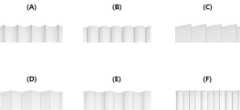
도 6을 참조하면, 도 2에서 A로 표시된 부분의 단면을 보인 것으로서, 본 실시형태에서 수지관(101)의 외면에는 다양한 단면형상을 가지는 요철(또는 메시)이 형성된다. 이러한 요철구조가 도 3 및 도 4의 수지관(101)에 적용될 수 있음은 물론이다.Referring to FIG. 6, as a cross-section of a portion indicated by A in FIG. 2 is shown, irregularities (or meshes) having various cross-sectional shapes are formed on the outer surface of the
이에 의하면, 수지관(101)과 강관(102)의 접합 시 접합강도를 향상시킬 수 있게 된다. 구체적으로 접착층에 의한 접합 또는 초음파 융착에 의한 접합 시 수지관(101) 외면의 요철 형상이 앙카링(anchoring) 역할을 하여 접착력을 증대시키게 된다.Accordingly, it is possible to improve the bonding strength when the
Claims (8)
Translated fromKorean상기 강관을 가공하여 준비하고, 상기 수지관의 길이방향 절개 없이 굽힘에 의한 탄성변형 및 복원이 가능한 재질로 구비되는 상기 수지관을 금형을 이용한 성형방법으로 성형하여 준비하는 제1 단계;
상기 수지관의 둘레면을 굽혀 탄성변형시켜 상기 강관의 내측에 삽입시킨 후, 상기 수지관의 탄성복원력에 의해 상기 수지관의 외면이 상기 강관의 내면에 밀착되게 위치시키는 제2 단계; 및
상기 수지관의 외면과 상기 강관의 내면을 접합하는 제3 단계;를 포함하고,
상기 수지관은, 탄성변형이 가능한 열가소성 수지 재질로 구비되고,
상기 수지관은, PTFE(Polytetrafluoroethylene), PFA(Perfluoroalkoxy), FEP(Fluorinated Ethylene Propylene), ETFE(Ethylene tetrafluoroethylene), ECTFE(ethylene chlorotrifluoroethylene), PVDF(polyvinylidene fluoride) 중에서 선택된 불소계열 수지로 구비되며,
상기 제2 단계는,
상기 수지관의 외면에 상기 강관의 내면과 접합성을 향상시키는 접착층을 더 형성하고,
상기 제3 단계는,
초음파 융착 수단을 이용하여 상기 수지관과 상기 강관의 계면 또는 상기 접착층에 초음파를 인가하여 상기 수지관과 상기 강관을 접합하는 반도체 공정용 이중관 제조방법.In the method for manufacturing a double pipe for a semiconductor process, which is formed of a steel pipe and a resin pipe fused to the inner surface of the steel pipe, and prevents the steel pipe from being corroded by contacting the steel pipe with a semiconductor process gas flowing inside the resin pipe,
A first step of preparing the steel pipe by processing and forming the resin pipe made of a material capable of elastic deformation and restoration by bending without longitudinal incision of the resin pipe by a molding method using a mold;
A second step of bending the circumferential surface of the resin pipe to elastically deform it and inserting it into the inside of the steel pipe, and then positioning the outer surface of the resin pipe to be in close contact with the inner surface of the steel pipe by the elastic restoring force of the resin pipe; And
A third step of bonding the outer surface of the resin pipe and the inner surface of the steel pipe; Including,
The resin tube is provided with a thermoplastic resin material capable of elastic deformation,
The resin tube is provided with a fluorine-based resin selected from PTFE (Polytetrafluoroethylene), PFA (Perfluoroalkoxy), FEP (Fluorinated Ethylene Propylene), ETFE (Ethylene tetrafluoroethylene), ECTFE (ethylene chlorotrifluoroethylene), PVDF (polyvinylidene fluoride),
The second step,
An adhesive layer is further formed on the outer surface of the resin pipe to improve bonding properties with the inner surface of the steel pipe,
The third step,
A method for manufacturing a double pipe for a semiconductor process in which ultrasonic waves are applied to the interface between the resin pipe and the steel pipe or the adhesive layer using an ultrasonic welding means to bond the resin pipe and the steel pipe.
상기 초음파 융착 수단은,
집속 초음파(focused ultrasound)를 이용하는 반도체 공정용 이중관 제조방법.The method according to claim 1,
The ultrasonic welding means,
A method of manufacturing a double tube for a semiconductor process using focused ultrasound.
상기 초음파 융착 수단은,
전력을 공급하는 전원부;
상기 전력을 이용하여 고주파 신호를 생성하는 고주파 생성부;
상기 고주파 신호를 이용하여 초음파를 생성하는 초음파 생성부; 및
상기 초음파를 집속하여 상기 수지관과 상기 강관의 계면에 고강도 집속 초음파를 인가하는 초음파 집속부;를 포함하는 반도체 공정용 이중관 제조방법.The method according to claim 1,
The ultrasonic welding means,
A power supply for supplying power;
A high frequency generator generating a high frequency signal using the power;
An ultrasonic generator for generating ultrasonic waves by using the high-frequency signal; And
An ultrasonic focusing unit for focusing the ultrasonic waves to apply high intensity focused ultrasonic waves to the interface between the resin pipe and the steel pipe.
상기 초음파 생성부는 적어도 두 개 이상으로 구성되고,
각각의 상기 초음파 생성부에서 생성되는 초음파의 전파(propagation) 방향을 제어하는 정렬부를 더 포함하는 반도체 공정용 이중관 제조방법.The method of claim 7,
The ultrasonic generator is composed of at least two or more,
A method of manufacturing a double tube for a semiconductor process further comprising an alignment unit for controlling a propagation direction of the ultrasonic waves generated by each of the ultrasonic generators.
Priority Applications (3)
| Application Number | Priority Date | Filing Date | Title |
|---|---|---|---|
| KR1020190165194AKR102218757B1 (en) | 2019-12-12 | 2019-12-12 | Manufacturing Method of Double Tube for Semiconductor Process |
| KR1020200134907AKR102449578B1 (en) | 2019-12-12 | 2020-10-19 | Double tube manufacturing method for semiconductor process |
| KR1020220060478AKR20220091437A (en) | 2019-12-12 | 2022-05-17 | Manufacturing Method of Double Tube for Semiconductor Process |
Applications Claiming Priority (1)
| Application Number | Priority Date | Filing Date | Title |
|---|---|---|---|
| KR1020190165194AKR102218757B1 (en) | 2019-12-12 | 2019-12-12 | Manufacturing Method of Double Tube for Semiconductor Process |
Related Child Applications (1)
| Application Number | Title | Priority Date | Filing Date |
|---|---|---|---|
| KR1020200134907ADivisionKR102449578B1 (en) | 2019-12-12 | 2020-10-19 | Double tube manufacturing method for semiconductor process |
Publications (1)
| Publication Number | Publication Date |
|---|---|
| KR102218757B1true KR102218757B1 (en) | 2021-02-22 |
Family
ID=74687556
Family Applications (3)
| Application Number | Title | Priority Date | Filing Date |
|---|---|---|---|
| KR1020190165194AActiveKR102218757B1 (en) | 2019-12-12 | 2019-12-12 | Manufacturing Method of Double Tube for Semiconductor Process |
| KR1020200134907AActiveKR102449578B1 (en) | 2019-12-12 | 2020-10-19 | Double tube manufacturing method for semiconductor process |
| KR1020220060478AWithdrawnKR20220091437A (en) | 2019-12-12 | 2022-05-17 | Manufacturing Method of Double Tube for Semiconductor Process |
Family Applications After (2)
| Application Number | Title | Priority Date | Filing Date |
|---|---|---|---|
| KR1020200134907AActiveKR102449578B1 (en) | 2019-12-12 | 2020-10-19 | Double tube manufacturing method for semiconductor process |
| KR1020220060478AWithdrawnKR20220091437A (en) | 2019-12-12 | 2022-05-17 | Manufacturing Method of Double Tube for Semiconductor Process |
Country Status (1)
| Country | Link |
|---|---|
| KR (3) | KR102218757B1 (en) |
Cited By (1)
| Publication number | Priority date | Publication date | Assignee | Title |
|---|---|---|---|---|
| KR20250066700A (en) | 2023-11-07 | 2025-05-14 | 비케이엠 주식회사 | Double Pipe having Flame-retardant Reinforcing Member for Semiconductor Process |
Citations (8)
| Publication number | Priority date | Publication date | Assignee | Title |
|---|---|---|---|---|
| JPH05272666A (en)* | 1992-03-25 | 1993-10-19 | Taihei Kogyo Co Ltd | Double pipe and its joint |
| JP2002357284A (en)* | 2001-06-01 | 2002-12-13 | Mitsubishi Rayon Co Ltd | Composite pipe |
| JP2007292136A (en)* | 2006-04-21 | 2007-11-08 | Hakubi Condex:Kk | Combined pipe manufacturing method and combined pipe manufactured using the same |
| KR100963423B1 (en)* | 2009-11-12 | 2010-06-15 | 현대하이스코 주식회사 | Method of manufacturing double-layer water pipe using hydro forming |
| JP2013231555A (en)* | 2012-04-27 | 2013-11-14 | Toshiba Corp | Centrifugal type thin film dryer |
| KR101350349B1 (en) | 2013-09-25 | 2014-01-13 | (주)보영테크 | Double pipe of semiconductor manufacturing process |
| KR20170015373A (en)* | 2014-06-10 | 2017-02-08 | 아이젠바우 크레이머 게엠베하 | Method for producing a multilayered large pipe |
| KR20190089170A (en)* | 2016-12-02 | 2019-07-30 | 스웨디쉬 매치 노스 유럽 에이비 | Method and apparatus for partial packaging of oral pouch snuff products |
- 2019
- 2019-12-12KRKR1020190165194Apatent/KR102218757B1/enactiveActive
- 2020
- 2020-10-19KRKR1020200134907Apatent/KR102449578B1/enactiveActive
- 2022
- 2022-05-17KRKR1020220060478Apatent/KR20220091437A/ennot_activeWithdrawn
Patent Citations (8)
| Publication number | Priority date | Publication date | Assignee | Title |
|---|---|---|---|---|
| JPH05272666A (en)* | 1992-03-25 | 1993-10-19 | Taihei Kogyo Co Ltd | Double pipe and its joint |
| JP2002357284A (en)* | 2001-06-01 | 2002-12-13 | Mitsubishi Rayon Co Ltd | Composite pipe |
| JP2007292136A (en)* | 2006-04-21 | 2007-11-08 | Hakubi Condex:Kk | Combined pipe manufacturing method and combined pipe manufactured using the same |
| KR100963423B1 (en)* | 2009-11-12 | 2010-06-15 | 현대하이스코 주식회사 | Method of manufacturing double-layer water pipe using hydro forming |
| JP2013231555A (en)* | 2012-04-27 | 2013-11-14 | Toshiba Corp | Centrifugal type thin film dryer |
| KR101350349B1 (en) | 2013-09-25 | 2014-01-13 | (주)보영테크 | Double pipe of semiconductor manufacturing process |
| KR20170015373A (en)* | 2014-06-10 | 2017-02-08 | 아이젠바우 크레이머 게엠베하 | Method for producing a multilayered large pipe |
| KR20190089170A (en)* | 2016-12-02 | 2019-07-30 | 스웨디쉬 매치 노스 유럽 에이비 | Method and apparatus for partial packaging of oral pouch snuff products |
Cited By (1)
| Publication number | Priority date | Publication date | Assignee | Title |
|---|---|---|---|---|
| KR20250066700A (en) | 2023-11-07 | 2025-05-14 | 비케이엠 주식회사 | Double Pipe having Flame-retardant Reinforcing Member for Semiconductor Process |
Also Published As
| Publication number | Publication date |
|---|---|
| KR20210074996A (en) | 2021-06-22 |
| KR20220091437A (en) | 2022-06-30 |
| KR102449578B1 (en) | 2022-09-30 |
Similar Documents
| Publication | Publication Date | Title |
|---|---|---|
| EP3030824B1 (en) | Method for the production of and high temperature field joints | |
| US5762741A (en) | Method for bonding polymeric articles | |
| KR102127009B1 (en) | Welding Device of Pipe for Semiconductor Manufacturing, And Production Method | |
| KR102218757B1 (en) | Manufacturing Method of Double Tube for Semiconductor Process | |
| CA2464969A1 (en) | The ultrasound welding of plastics components | |
| AU2012331694B2 (en) | Pipeline unit | |
| GB2520717A (en) | Techniques for coating pipeline field joints | |
| US8287679B2 (en) | Method for forming a protective coat about a cutback between pipes forming part of an underwater pipeline | |
| KR100446547B1 (en) | Synthetic resin pipe joint with metal connecting member and manufacturing method | |
| KR20210017984A (en) | Pipe for Semiconductor Manufacturing | |
| JP2012030559A (en) | Joining method using laser beam | |
| CN114571644B (en) | Combined type closed impeller with perfluor surface | |
| KR102449426B1 (en) | Equipment for welding large diameter pvc pipe | |
| JP4965213B2 (en) | Method for welding modified polytetrafluoroethylene molded body | |
| JP6264959B2 (en) | Manufacturing method of high-pressure tank | |
| AU2012331693B2 (en) | Pipeline unit | |
| JP2008204798A (en) | Plasma processing method, electrode structure, and plasma processing apparatus | |
| JP2004251368A (en) | Manufacturing method for seat ring for valve, and manufacturing method for valve element | |
| JPH06134869A (en) | Method for connecting fluorine resin | |
| TWI762213B (en) | Fluororesin storage tank and manufacturing method thereof | |
| TWI823827B (en) | A manufacturing method of a fluororesin membrane distillation device, a repairing method and the production thereof | |
| US11565481B2 (en) | Method of welding additively manufactured thermoplastic | |
| KR20240074580A (en) | Double pipe for semiconductor and display process and manufacturing method thereof | |
| JPH03124592A (en) | Fluororesin lined container and manufacture thereof | |
| JP2004019811A (en) | Refrigerant low-permeable compound sealing material and manufacturing method for it |
Legal Events
| Date | Code | Title | Description |
|---|---|---|---|
| PA0109 | Patent application | Patent event code:PA01091R01D Comment text:Patent Application Patent event date:20191212 | |
| PA0201 | Request for examination | ||
| PA0302 | Request for accelerated examination | Patent event date:20191212 Patent event code:PA03022R01D Comment text:Request for Accelerated Examination | |
| PE0902 | Notice of grounds for rejection | Comment text:Notification of reason for refusal Patent event date:20200504 Patent event code:PE09021S01D | |
| AMND | Amendment | ||
| PE0601 | Decision on rejection of patent | Patent event date:20200917 Comment text:Decision to Refuse Application Patent event code:PE06012S01D Patent event date:20200504 Comment text:Notification of reason for refusal Patent event code:PE06011S01I | |
| AMND | Amendment | ||
| PA0107 | Divisional application | Comment text:Divisional Application of Patent Patent event date:20201019 Patent event code:PA01071R01D | |
| PX0901 | Re-examination | Patent event code:PX09011S01I Patent event date:20200917 Comment text:Decision to Refuse Application Patent event code:PX09012R01I Patent event date:20200706 Comment text:Amendment to Specification, etc. | |
| PX0701 | Decision of registration after re-examination | Patent event date:20210215 Comment text:Decision to Grant Registration Patent event code:PX07013S01D Patent event date:20201019 Comment text:Amendment to Specification, etc. Patent event code:PX07012R01I Patent event date:20200917 Comment text:Decision to Refuse Application Patent event code:PX07011S01I Patent event date:20200706 Comment text:Amendment to Specification, etc. Patent event code:PX07012R01I | |
| X701 | Decision to grant (after re-examination) | ||
| GRNT | Written decision to grant | ||
| PR0701 | Registration of establishment | Comment text:Registration of Establishment Patent event date:20210216 Patent event code:PR07011E01D | |
| PR1002 | Payment of registration fee | Payment date:20210216 End annual number:3 Start annual number:1 | |
| PG1601 | Publication of registration |