KR102214996B1 - Power system - Google Patents
Power systemDownload PDFInfo
- Publication number
- KR102214996B1 KR102214996B1KR1020190019185AKR20190019185AKR102214996B1KR 102214996 B1KR102214996 B1KR 102214996B1KR 1020190019185 AKR1020190019185 AKR 1020190019185AKR 20190019185 AKR20190019185 AKR 20190019185AKR 102214996 B1KR102214996 B1KR 102214996B1
- Authority
- KR
- South Korea
- Prior art keywords
- power
- module
- motherboard
- pin
- control unit
- Prior art date
- Legal status (The legal status is an assumption and is not a legal conclusion. Google has not performed a legal analysis and makes no representation as to the accuracy of the status listed.)
- Active
Links
Images


Classifications
- H—ELECTRICITY
- H05—ELECTRIC TECHNIQUES NOT OTHERWISE PROVIDED FOR
- H05K—PRINTED CIRCUITS; CASINGS OR CONSTRUCTIONAL DETAILS OF ELECTRIC APPARATUS; MANUFACTURE OF ASSEMBLAGES OF ELECTRICAL COMPONENTS
- H05K7/00—Constructional details common to different types of electric apparatus
- H05K7/14—Mounting supporting structure in casing or on frame or rack
- H05K7/1417—Mounting supporting structure in casing or on frame or rack having securing means for mounting boards, plates or wiring boards
- H—ELECTRICITY
- H02—GENERATION; CONVERSION OR DISTRIBUTION OF ELECTRIC POWER
- H02M—APPARATUS FOR CONVERSION BETWEEN AC AND AC, BETWEEN AC AND DC, OR BETWEEN DC AND DC, AND FOR USE WITH MAINS OR SIMILAR POWER SUPPLY SYSTEMS; CONVERSION OF DC OR AC INPUT POWER INTO SURGE OUTPUT POWER; CONTROL OR REGULATION THEREOF
- H02M7/00—Conversion of AC power input into DC power output; Conversion of DC power input into AC power output
- H02M7/003—Constructional details, e.g. physical layout, assembly, wiring or busbar connections
- H—ELECTRICITY
- H02—GENERATION; CONVERSION OR DISTRIBUTION OF ELECTRIC POWER
- H02M—APPARATUS FOR CONVERSION BETWEEN AC AND AC, BETWEEN AC AND DC, OR BETWEEN DC AND DC, AND FOR USE WITH MAINS OR SIMILAR POWER SUPPLY SYSTEMS; CONVERSION OF DC OR AC INPUT POWER INTO SURGE OUTPUT POWER; CONTROL OR REGULATION THEREOF
- H02M7/00—Conversion of AC power input into DC power output; Conversion of DC power input into AC power output
- H02M7/02—Conversion of AC power input into DC power output without possibility of reversal
- H02M7/04—Conversion of AC power input into DC power output without possibility of reversal by static converters
- H—ELECTRICITY
- H02—GENERATION; CONVERSION OR DISTRIBUTION OF ELECTRIC POWER
- H02M—APPARATUS FOR CONVERSION BETWEEN AC AND AC, BETWEEN AC AND DC, OR BETWEEN DC AND DC, AND FOR USE WITH MAINS OR SIMILAR POWER SUPPLY SYSTEMS; CONVERSION OF DC OR AC INPUT POWER INTO SURGE OUTPUT POWER; CONTROL OR REGULATION THEREOF
- H02M7/00—Conversion of AC power input into DC power output; Conversion of DC power input into AC power output
- H—ELECTRICITY
- H05—ELECTRIC TECHNIQUES NOT OTHERWISE PROVIDED FOR
- H05K—PRINTED CIRCUITS; CASINGS OR CONSTRUCTIONAL DETAILS OF ELECTRIC APPARATUS; MANUFACTURE OF ASSEMBLAGES OF ELECTRICAL COMPONENTS
- H05K7/00—Constructional details common to different types of electric apparatus
- H05K7/14—Mounting supporting structure in casing or on frame or rack
- H05K7/1422—Printed circuit boards receptacles, e.g. stacked structures, electronic circuit modules or box like frames
- H—ELECTRICITY
- H05—ELECTRIC TECHNIQUES NOT OTHERWISE PROVIDED FOR
- H05K—PRINTED CIRCUITS; CASINGS OR CONSTRUCTIONAL DETAILS OF ELECTRIC APPARATUS; MANUFACTURE OF ASSEMBLAGES OF ELECTRICAL COMPONENTS
- H05K7/00—Constructional details common to different types of electric apparatus
- H05K7/14—Mounting supporting structure in casing or on frame or rack
- H05K7/1485—Servers; Data center rooms, e.g. 19-inch computer racks
Landscapes
- Engineering & Computer Science (AREA)
- Power Engineering (AREA)
- Microelectronics & Electronic Packaging (AREA)
- Computer Hardware Design (AREA)
- General Engineering & Computer Science (AREA)
- Charge And Discharge Circuits For Batteries Or The Like (AREA)
Abstract
Translated fromKoreanDescription
Translated fromKorean본 개시는 전력 시스템에 관한 것으로서, 더욱 구체적으로는 로봇과 같은 장치에 탑재되어 다양한 부하에 다양한 정류의 전력을 공급하는 전력 시스템에 관한 것이다.The present disclosure relates to a power system, and more particularly, to a power system that is mounted on a device such as a robot and supplies various rectified power to various loads.
다양한 종류의 로봇들이 개발되고 있다. 로봇들은 개발 목적에 따라 스스로 이동하거나, 물건을 옮기거나, 사용자에게 정보를 제공하거나, 주변을 촬영하거나, 직접 채취한 시료를 분석하는 등 다양한 기능을 수행할 수 있다. 그에 따라 로봇들은 그들의 목적에 따라 다양한 종류의 전기 장치를 탑재하고 있으며, 이러한 전기 장치는 그 목적에 따라 설계된 전력을 공급받아야 한다. 이러한 전기 장치들을 포함하는 장치를 개발할 경우, 각각의 전기 장치에 맞는 전력을 공급하기 위한 전력 시스템도 함께 개발 및 제조되어야 한다.Various types of robots are being developed. Depending on the purpose of development, robots can perform various functions, such as moving by themselves, moving objects, providing information to users, photographing the surroundings, or analyzing directly collected samples. Accordingly, robots are equipped with various types of electric devices according to their purpose, and these electric devices must be supplied with power designed according to the purpose. When developing a device including these electrical devices, a power system for supplying power suitable for each electrical device must also be developed and manufactured.
본 개시의 다양한 실시예들이 해결하고자 하는 과제는 다양한 종류의 전력을 적응적으로 공급하면서도 작은 부피를 차지하는 전력 시스템을 제공하는 것이다.A problem to be solved by various embodiments of the present disclosure is to provide a power system that adaptively supplies various types of power and occupies a small volume.
상술한 기술적 과제들을 달성하기 위한 기술적 수단으로서, 본 개시의 제1 측면에 따른 전력 시스템은 마더보드 및 상기 마더보드 상에 순차적으로 적층될 수 있는 복수의 전력 모듈을 포함한다. 상기 마더보드는 마더보드 기판, 및 상기 마더보드 기판 상의 전력핀을 포함하고, 상기 전력핀을 통해 메인 전력을 공급하도록 구성된다. 상기 복수의 전력 모듈은 제1 모듈 기판 및 상기 제1 모듈 기판을 관통하는 제1 관통 전력핀을 포함하고, 상기 마더보드 상에 적층되어 상기 제1 관통 전력핀이 상기 마더보드의 상기 전력핀에 연결되면, 상기 메인 전력으로부터 제1 전력을 변환하여 출력하는 제1 전력 모듈, 및 제2 모듈 기판 및 상기 제2 모듈 기판을 관통하는 제2 관통 전력핀을 포함하고, 상기 제1 전력 모듈 상에 적층되어 상기 제2 관통 전력핀이 상기 제1 전력 모듈의 상기 제1 관통 전력핀에 연결되면, 상기 메인 전력으로부터 제2 전력을 변환하여 출력하는 제2 전력 모듈을 포함한다.As a technical means for achieving the above technical problems, the power system according to the first aspect of the present disclosure includes a motherboard and a plurality of power modules that may be sequentially stacked on the motherboard. The motherboard includes a motherboard substrate and a power pin on the motherboard substrate, and is configured to supply main power through the power pin. The plurality of power modules includes a first module substrate and a first through power pin penetrating through the first module substrate, and is stacked on the motherboard so that the first through power pin is connected to the power pin of the motherboard. When connected, a first power module for converting and outputting a first power from the main power, and a second module substrate and a second through power pin penetrating through the second module substrate, on the first power module And a second power module that is stacked and converts and outputs second power from the main power when the second through power pin is connected to the first through power pin of the first power module.
본 개시의 제2 측면에 따른 전력 시스템은 마더보드 및 상기 마더보드 상에 탈착 가능하게 결합되는 제1 전력 모듈을 포함한다. 상기 마더보드는 마더보드 기판, 및 상기 마더보드 기판 상의 전력핀을 포함하고, 상기 전력핀을 통해 메인 전력을 공급한다. 상기 제1 전력 모듈은 제1 모듈 기판 및 상기 제1 모듈 기판을 관통하는 제1 관통 전력핀을 포함하고, 상기 마더보드 상에 적층되어 상기 제1 관통 전력핀이 상기 마더보드의 상기 전력핀에 연결되면, 상기 메인 전력으로부터 제1 전력을 변환하여 출력한다. 상기 제1 관통 전력핀은 상기 제1 전력 모듈 상에 탈착 가능하게 결합되는 다른 전력 모듈이 접속할 수 있도록 접점을 제공한다.A power system according to a second aspect of the present disclosure includes a motherboard and a first power module detachably coupled to the motherboard. The motherboard includes a motherboard substrate and a power pin on the motherboard substrate, and supplies main power through the power pin. The first power module includes a first module substrate and a first through power pin penetrating through the first module substrate, and is stacked on the motherboard so that the first through power pin is connected to the power pin of the motherboard. When connected, the first power is converted from the main power and output. The first through power pin provides a contact point so that another power module detachably coupled to the first power module can be connected.
본 개시의 다양한 실시예들에 따른 전력 시스템은 마더보드 상에 서로 다른 종류의 부하 전력을 공급하도록 구성되는 복수의 전력 모듈이 적층되므로, 본 개시에 따른 전력 시스템을 채용한 전체 시스템의 다양한 종류의 부하들에 적응적으로 전력을 공급할 수 있다. 또한, 전력 모듈들은 서로 적층되는 방식으로 마더보드 상에 배치되므로, 전력 시스템은 적은 부피를 차지할 수 있다. 뿐만 아니라, 전체 시스템을 새롭게 개발하는 경우, 전력 시스템을 새로 개발하지 않아도 되므로, 개발 기간과 비용을 줄일 수 있다.In the power system according to various embodiments of the present disclosure, since a plurality of power modules configured to supply different types of load power are stacked on the motherboard, various types of the entire system employing the power system according to the present disclosure It can adaptively supply power to loads. Also, since the power modules are disposed on the motherboard in a stacked manner, the power system can occupy a small volume. In addition, when the entire system is newly developed, it is not necessary to develop a new power system, so that the development period and cost can be reduced.
도 1은 일 실시예에 따른 전력 시스템의 측면을 개략적으로 도시한다.
도 2는 도 1의 전력 시스템의 다른 측면을 개략적으로 도시한다.
도 3은 일 실시예에 따라서 마더보드의 제1 타입의 핀 및 전력 모듈의 관통핀들 간의 연결을 도시하기 위한 일부 확대도이다.
도 4는 일 실시예에 따라서 전력 모듈의 개략적인 단면도를 도시한다.
도 5는 일 실시예에 따른 전력 시스템의 전체 구성을 개략적으로 도시한다.
도 6은 일 실시예에 따른 마더보드의 구성을 개략적으로 도시한다.
도 7은 일 실시예에 따른 전력 모듈의 구성을 개략적으로 도시한다.
도 8은 일 실시예에 따른 마더보드의 구성을 도시한다.
도 9는 일 실시예에 따른 전력 모듈의 구성을 도시한다.
도 10은 다른 실시예에 따른 전력 시스템의 전체 구성을 개략적으로 도시한다.
도 11은 다른 실시예에 따른 마더보드의 구성을 개략적으로 도시한다.
도 12는 다른 실시예에 따른 전력 모듈의 구성을 개략적으로 도시한다.
도 13은 일 실시예에 따라서 마더보드와 전력 모듈들 간의 데이터 통신을 수행하기 위한 구성도를 도시한다.
도 14는 일 실시예에 따라서 전력 모듈이 적층 순서에 해당하는 ID를 자동으로 할당하는 방법을 설명하기 위한 예시적인 도면이다
도 15는 다른 실시예에 따라서 전력 모듈이 적층 순서에 해당하는 ID를 자동으로 할당하는 방법을 설명하기 위한 예시적인 도면이다.
도 16은 일 실시예에 따라서 전력 모듈이 마지막으로 적층되었음을 감지하기 위한 구성을 개략적으로 도시한다.
도 17은 일 실시예에 따라서 모듈 MCU의 데이터 출력 단자의 구성을 개략적으로 도시한다.
도 18은 또 다른 실시예에 따른 전력 시스템을 개략적으로 도시한다.1 schematically shows a side view of a power system according to an embodiment.
Figure 2 schematically shows another aspect of the power system of Figure 1;
3 is an enlarged view illustrating a connection between pins of a first type of a motherboard and through pins of a power module according to an exemplary embodiment.
4 shows a schematic cross-sectional view of a power module according to an embodiment.
5 schematically shows the overall configuration of a power system according to an embodiment.
6 schematically shows a configuration of a motherboard according to an embodiment.
7 schematically shows a configuration of a power module according to an embodiment.
8 shows a configuration of a motherboard according to an embodiment.
9 shows a configuration of a power module according to an embodiment.
10 schematically shows the overall configuration of a power system according to another embodiment.
11 schematically shows a configuration of a motherboard according to another embodiment.
12 schematically shows a configuration of a power module according to another embodiment.
13 illustrates a configuration diagram for performing data communication between a motherboard and power modules according to an embodiment.
14 is an exemplary diagram for describing a method of automatically allocating an ID corresponding to a stacking order by a power module according to an embodiment
15 is an exemplary diagram for explaining a method of automatically allocating an ID corresponding to a stacking order by a power module according to another embodiment.
16 schematically shows a configuration for detecting that a power module is last stacked according to an embodiment.
17 schematically shows a configuration of a data output terminal of a module MCU according to an embodiment.
18 schematically shows a power system according to another embodiment.
아래에서는 첨부한 도면을 참조하여 본 개시가 속하는 기술 분야에서 통상의 지식을 가진 자가 용이하게 실시할 수 있도록 다양한 실시예들을 상세히 설명한다. 그러나 본 개시의 기술적 사상은 다양한 형태로 변형되어 구현될 수 있으므로 본 명세서에서 설명하는 실시예들로 제한되지 않는다. 본 개시의 다양한 실시예들을 설명함에 있어서 관련된 공지 기술을 구체적으로 설명하는 것이 본 개시의 기술적 사상의 요지를 흐릴 수 있다고 판단되는 경우 그 공지 기술에 대한 구체적인 설명을 생략한다. 동일하거나 유사한 구성요소는 동일한 참조 번호를 부여하고 이에 대한 중복되는 설명은 생략하기로 한다.Hereinafter, various exemplary embodiments will be described in detail with reference to the accompanying drawings so that those of ordinary skill in the art may easily implement the present disclosure. However, the technical idea of the present disclosure may be modified and implemented in various forms, and thus is not limited to the embodiments described herein. In describing various embodiments of the present disclosure, when it is determined that a detailed description of a related known technology may obscure the spirit of the present disclosure, a detailed description of the known technology will be omitted. The same or similar components are given the same reference numerals, and redundant descriptions thereof will be omitted.
명세서 전체에서, 어떤 요소가 다른 요소와 "연결"되어 있다고 할 때, 이는 "직접적으로 연결"되어 있는 경우뿐 아니라, 그 중간에 다른 요소를 사이에 두고 "전기적으로 연결"되어 있는 경우도 포함한다. 어떤 요소가 다른 요소를 "포함"한다고 할 때, 이는 특별히 반대되는 기재가 없는 한 다른 요소 외에 또 다른 요소를 배제하는 것이 아니라, 또 다른 요소를 더 포함할 수 있는 것을 의미한다.Throughout the specification, when an element is said to be “connected” to another element, this includes not only the case that it is “directly connected”, but also the case that it is “electrically connected” with another element in between. . When a certain element "includes" another element, it means that another element may be further included, rather than excluding another element other than the other element unless specifically stated to the contrary.
일부 실시예들은 기능적인 블록 구성들 및 다양한 처리 단계들로 설명될 수 있다. 이러한 기능 블록들의 일부 또는 전부는 특정 기능을 실행하는 다양한 개수의 하드웨어 및/또는 소프트웨어 구성들로 구현될 수 있다. 예를 들어, 본 개시의 기능 블록들은 하나 이상의 마이크로프로세서들에 의해 구현되거나, 소정의 기능을 위한 회로 구성들에 의해 구현될 수 있다. 본 개시의 기능 블록들은 다양한 프로그래밍 언어 또는 스크립트 언어(scripting language)로 구현될 수 있다. 본 개시의 기능 블록들은 하나 이상의 프로세서들에서 실행되는 알고리즘으로 구현될 수 있다. 본 개시의 기능 블록이 수행하는 기능은 복수의 기능 블록에 의해 수행되거나, 본 개시에서 복수의 기능 블록이 수행하는 기능들은 하나의 기능 블록에 의해 수행될 수도 있다.Some embodiments may be described with functional block configurations and various processing steps. Some or all of these functional blocks may be implemented with various numbers of hardware and/or software components that perform a specific function. For example, the functional blocks of the present disclosure may be implemented by one or more microprocessors, or may be implemented by circuit configurations for a predetermined function. Functional blocks of the present disclosure may be implemented in various programming languages or scripting languages. The functional blocks of the present disclosure may be implemented as an algorithm executed on one or more processors. Functions performed by a function block of the present disclosure may be performed by a plurality of function blocks, or functions performed by a plurality of function blocks in the present disclosure may be performed by a single function block.
도면에 도시된 요소들 간의 연결 선 또는 연결 부재들은 기능적 연결 및/또는 물리적 또는 회로적 연결들을 예시적으로 나타낸 것일 뿐이다. 실제 장치에서는 대체 가능하거나 추가되는 다양한 기능적 연결, 물리적 연결, 또는 회로적 연결에 의해 요소들 간의 연결이 구현될 수 있다.Connection lines or connecting members between elements shown in the drawings are merely illustrative of functional connections and/or physical or circuit connections. In an actual device, connections between elements may be implemented by various functional connections, physical connections, or circuit connections that can be replaced or added.
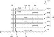
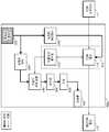
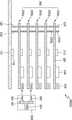
도 1은 일 실시예에 따른 전력 시스템의 측면을 개략적으로 도시한다. 도 2는 도 1의 전력 시스템의 다른 측면을 개략적으로 도시한다.1 schematically shows a side view of a power system according to an embodiment. Figure 2 schematically shows another aspect of the power system of Figure 1;
도 1 및 도 2를 참조하면, 전력 시스템(1000)은 마더보드(100) 및 마더보드(100) 상에 순차적으로 적층될 수 있는 전력 모듈들(200a-200e, 200)을 포함한다. 전력 모듈들(200a-200e, 200)은 마더보드(100) 또는 다른 전력 모듈들(200) 상에 적층 방식으로 결합되거나, 마더보드(100) 또는 다른 전력 모듈들(200)로부터 분리될 수도 있다. 전력 모듈들(200a-200e, 200)은 필요에 따라 다른 순서로 마더보드(100) 상에 적층될 수 있다. 전력 모듈들(200a-200e, 200)의 적층 순서는 본 발명을 한정하지 않는다.1 and 2, the
전력 모듈들(200a-200e, 200)은 서로 다른 전력을 출력할 수 있다. 예를 들면, 제1 및 제2 전력 모듈(200a, 200b)은 12V의 전압을 출력하고, 제3 전력 모듈(200c)은 5V의 전압을 출력하고, 제4 및 제5 전력 모듈(200d, 200e)은 9V의 전압을 출력할 수 있다. 전술한 수치는 오로지 예시적이다. 도 1에서 마더보드(100) 상에 5개의 전력 모듈들(200a-200e, 200)이 적층된 것으로 도시되지만, 이 역시 예시적이며, 더 적거나 더 많은 개수의 전력 모듈들(200)이 마더보드(100) 상에 적층될 수 있다. 또한, 도 1에 예시적으로 도시되는 전력 모듈들(200a-200e)은 통칭하여 전력 모듈(200)로 지칭될 수 있다.The
전력 시스템(1000)은 전기 장치에 장착되어, 전기 장치의 여러 종류의 부하들에 전력을 공급할 수 있다. 전력 시스템(1000)이 탑재되는 전기 장치는 예컨대 로봇 장치일 수 있다. 로봇 장치는 이동할 수 있으며, 설계에 따라 다양한 기능을 수행할 수 있다. 로봇 장치는 비슷한 외형을 갖더라도, 내부에 장착된 기능 장치들에 따라 다른 기능을 수행할 수 있다. 그에 따라, 다양한 전력이 공급될 필요가 있다. 본 발명에 따른 전력 시스템(100)은 다양한 전력을 각각 공급하는 전력 모듈들(200)을 마더보드(100) 상에 적층하는 구조를 가짐에 따라, 로봇 장치와 같은 전기 장치에서 필요로 하는 전력을 쉽게 제공할 수 있다. 본 명세서에서는 전력 시스템(1000)이 탑재되는 전기 장치를 로봇 장치라고 지칭한다. 그러나, 이는 오로지 한가지 예일 뿐이며, 본 발명을 한정하지 않는다.The
도 1과 도 2에서 전력 모듈들(200)은 마더보드(100)의 위쪽에 배치되는 것으로 도시되어 있지만, 전력 모듈들(200)은 마더보드(100)의 측면으로 적층될 수 있다.In FIGS. 1 and 2, the
마더보드(100)는 마더보드 기판(101), 적어도 하나의 제1 타입의 핀(120), 적어도 하나의 제2 타입의 핀(130) 및 마더보드 제어부(110)를 포함할 수 있다. 제1 타입의 핀(120)은 메인 전력을 공급하는 전력핀(120)을 포함할 수 있다. 제2 타입의 핀(130)은 마더보드 제어부(110)와 모듈 제어부들(210) 사이의 데이터 통신을 위한 통신핀을 포함할 수 있다. 마더보드 제어부(110)는 마더보드(100)의 전체적인 기능을 제어할 수 있다. 마더보드 제어부(110)는 전력 모듈들(200)의 모듈 제어부들(210)과 통신하여 전력 모듈들(200)을 제어하거나 전력 모듈들(200)의 상태를 수신할 수 있다.The
마더보드(100)는 배터리 또는 충전기에 연결될 수 있다. 메인 전력은 배터리로부터 출력되는 배터리 전력 또는 충전기로부터 공급되는 충전 전력을 의미할 수 있다. 예컨대, 충전기가 마더보드(100)에 연결되는 경우, 메인 전력은 충전 전력을 지칭하고, 충전기가 마더보드(100)로부터 분리되는 경우, 메인 전력은 배터리 전력을 지칭할 수 있다.The
전력 모듈들(200) 각각은 모듈 기판(201), 적어도 하나의 관통핀(220), 적어도 하나의 하부핀(230b), 적어도 하나의 상부핀(230t), 모듈 제어부(210), 및 전력 변환부(240)를 포함할 수 있다. 관통핀(220)은 모듈 기판(201)을 관통하며, 전력 모듈(200)이 마더보드(100) 상에 적층되면, 관통핀(220)은 제1 타입의 핀(120)과 접촉할 수 있다. 전력 모듈들(200)이 서로 적층되는 경우, 서로 적층되는 전력 모듈들(200)의 관통핀(220)은 서로 접촉할 수 있다. 관통핀(220)은 마더보드(100)의 전력핀(120)과 접촉하는 전력 관통핀(220)을 포함할 수 있다.Each of the
하부핀(230b)과 상부핀(230t)은 모듈 기판(201)의 표면에 배치되는 표면 장착 타입(surface mount type)의 전기 단자로서, 전력 모듈(200)이 마더보드(100) 상에 적층되면, 하부핀(230b)은 제2 타입의 핀(130)과 접촉할 수 있다. 전력 모듈들(200)이 서로 적층되는 경우, 아래에 위치한 전력 모듈(200)의 상부핀(230t)은 상부에 적층되는 전력 모듈(200)의 하부핀(230b)과 접촉될 수 있다. 적어도 하나의 하부핀(230b)과 적어도 하나의 상부핀(230t)은 서로 대응되는 위치에 배치되어, 전력 모듈들(200)이 적층되면 서로 접촉할 수 있다.The
모듈 제어부(210)는 전력 모듈(200)의 전체적인 동작을 제어할 수 있다. 모듈 제어부(210)는 하부핀(230b)과 상부핀(230t) 및/또는 관통핀(220)을 이용하여 마더보드 제어부(110) 및 다른 전력 모듈(200)의 모듈 제어부들(210)과 데이터 통신을 할 수 있다. 모듈 제어부(210)는 마더보드 제어부(110)의 제어에 따라 전력 모듈(200)을 제어하고, 전력 모듈(200)의 상태를 마더보드 제어부(110)에 전송할 수 있다.The
전력 변환부(240)는 전력핀(120)과 접촉하는 관통핀(220)을 통해 공급되는 메인 전력으로부터 전력 모듈(200)의 설계에 따라 설정된 부하 전력을 출력할 수 있다. 전력 변환부(240)에 의해 생성되는 부하 전력은 로봇 장치의 전기 부하에 공급될 수 있다. 전력 모듈들(200)의 전력 변환부(240)는 서로 다른 부하 전력을 출력할 수 있다. 전술한 예에서와 같이, 제1 및 제2 전력 모듈(200a, 200b)의 전력 변환부(240)는 메인 전력으로부터 12V의 부하 전력을 생성하여 출력하고, 제3 전력 모듈(200c)은 메인 전력으로부터 5V의 부하 전력을 생성하여 출력하고, 제4 및 제5 전력 모듈(200d, 200e)은 메인 전력으로부터 9V의 부하 전력을 생성하여 출력할 수 있다. 이와 같이, 전력 모듈들(220) 중 적어도 일부에서 출력되는 부하 전력들의 전압 레벨은 서로 상이할 수 있다.The
마더보드(100)의 제1 타입의 핀(120)은 전력 모듈(200)이 마더보드(100) 상에 적층될 때 전력 모듈(200)의 관통핀(220)과 전기적으로 연결되는 핀들을 의미한다. 마더보드(100)의 제2 타입의 핀(130)은 전력 모듈(200)이 마더보드(100) 상에 적층될 때 전력 모듈(200)의 하부핀(230b)과 전기적으로 연결되는 핀들을 의미한다.The first type of
제1 타입의 핀(120) 및 관통핀들(220)은 메인 전력, 접지 등을 전달하는 전력 전송 기능을 할 수 있다. 큰 전류를 갖는 메인 전력을 전송하기 위하여 공통으로 접속되는 복수의 제1 타입의 핀(120) 및 복수의 관통핀들(220)이 사용될 수 있다. 제1 타입의 핀(120) 및 관통핀들(220)은 마더보드 제어부(110)에 수신되는 데이터 신호, 클럭 신호, 칩 선택 신호 등을 전달하는 통신 기능을 수행할 수 있다. 제2 타입의 핀(130) 및 하부핀들(230b)과 상부핀들(230t)은 마더보드 제어부(110)로부터 송신되는 데이터 신호 등을 전달하는 통신 기능을 수행할 수 있다. 전력 모듈(200)의 하부핀(230b)과 상부핀(230t)은 전력 모듈(200)이 마지막으로 적층된 것인지를 판별하기 위한 기능을 수행하는데 사용될 수 있다. 통신 접지는 제1 타입의 핀(120) 및 관통핀들(220)을 통해 연결되거나, 제2 타입의 핀(130) 및 하부핀들(230b)과 상부핀들(230t)을 통해 연결될 수 있다.The first type of
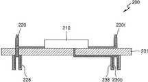
도 3은 일 실시예에 따라서 마더보드의 제1 타입의 핀 및 전력 모듈의 관통핀들 간의 연결을 도시하기 위한 일부 확대도이다.3 is an enlarged view illustrating a connection between pins of a first type of a motherboard and through pins of a power module according to an exemplary embodiment.
도 3을 참조하면, 마더보드 기판(101)의 일부 및 모듈 기판(201)의 일부가 도시된다. 마더보드 기판(101) 상에는 제1 타입의 핀들(도 2의 120)이 장착되는 커넥터(120c)가 장착된다. 모듈 기판(201) 상에도 역시 관통핀들(도 2의 220)이 장착되는 커넥터(220c)이 장착된다. 도 3에 도시된 바와 같이, 전력 모듈(200)이 마더보드(100) 상에 적층되기 위해서는 커넥터들(120c, 220c)이 서로 결합되어야 하며, 관통핀들(220)은 대응하는 위치에 배치되는 제1 타입의 핀들(120)과 접촉하게 된다.Referring to FIG. 3, a part of the
도 3에는 제1 타입의 핀 및 관통핀들이 도시되지만, 제2 타입의 핀(도 2의 130) 및 하부핀(도 2의 230b)과 상부핀(도 2의 230t)도 커넥터를 통해 서로 연결될 수 있다.Although the first type of pin and the through pin are shown in FIG. 3, the second type of pin (130 in FIG. 2), the lower pin (230b in FIG. 2) and the upper pin (230t in FIG. 2) are also connected to each other through a connector. I can.
도 4는 일 실시예에 따라서 전력 모듈의 개략적인 단면도를 도시한다.4 shows a schematic cross-sectional view of a power module according to an embodiment.
도 4를 참조하면, 전력 모듈(200)은 모듈 기판(201) 상의 모듈 제어부(210), 모듈 기판(201)을 관통하는 관통핀(220), 모듈 기판(201)의 상부 표면 상의 상부핀(230t) 및 모듈 기판(201)의 하부 표면 상의 하부핀(230b)을 포함한다. 관통핀(220)의 아래 부분은 하우징(228)으로 둘러싸여 커넥터를 형성할 수 있다. 하부핀(230b)은 하우징(230)으로 둘러싸여 커넥터를 형성할 수 있으며, 하부핀(230b)은 아래에 배치되는 모듈 기판(201)의 상부핀(230t)과 접촉할 수 있다.Referring to FIG. 4, the
관통핀(220)과 상부핀(230t), 하부핀(230b)은 모두 모듈 제어부(210)에 연결될 수 있다. 모듈 제어부(210)가 상부 표면에 배치되는 경우, 하부핀(230b)은 모듈 기판(201)을 관통하는 배선을 통해 모듈 제어부(210)에 연결될 수 있다.The through
도 1 및 도 2에는 마더보드(100) 상에 복수의 전력 모듈들(200a-200e, 200)이 적층되는 것으로 도시되지만, 다른 실시예에 따르면, 전력 시스템(1000)은 마더보드(100) 및 마더보드(100) 상에 적층된 하나의 전력 모듈(예컨대, 200a)을 포함할 수도 있다. 전력 모듈(200a)은 마더 보드(100) 상에 탈착 가능하게 결합된다. 마더보드(100)는 마더보드 기판(101), 및 마더보드 기판(101) 상의 전력핀(120)을 포함할 수 있으며, 마더보드(1000)는 전력핀(120)을 통해 메인 전력을 전력 모듈(200a)에 공급할 수 있다.1 and 2 shows that a plurality of
전력 모듈(200a)은 모듈 기판(201), 및 모듈 기판(201)을 관통하는 관통 전력핀(220)을 포함한다. 전력 모듈(200a)이 마더보드(100) 상에 적층되어 관통 전력핀(220)이 전력핀(120)에 연결되면, 전력 모듈(200a)은 메인 전력으로부터 제1 전력을 변환하여 출력할 수 있다. 관통 전력핀(220)은 모듈 기판(201)을 관통하므로, 모듈 기판(201)의 저면으로부터 돌출되는 하부 부분과 모듈 기판(201)의 상면으로부터 돌출되는 상부 부분을 갖는다. 관통 전력핀(220)의 하부 부분은 마더보드(100)의 전력핀(120)과 접촉하며, 관통 전력핀(220)의 상부 부분은 전력 모듈(200a) 상에 탈착 가능하게 결합되는 다른 전력 모듈이 접속할 수 있는 접점을 제공할 수 있다.The
또 다른 실시예에 따르면, 마더보드(100) 상에 2개의 전력 모듈(예컨대, 제1 전력 모듈(200a)과 제2 전력 모듈(200b))이 적층될 수도 있다. 제2 전력 모듈(200b)은 제1 전력 모듈(200a) 상에 탈착 가능하게 결합될 수 있다. 제2 전력 모듈(200b)도 모듈 기판(201 및 모듈 기판(201)을 관통하는 관통 전력핀(220)을 포함한다.According to another embodiment, two power modules (eg, a
제2 전력 모듈(200b)이 제1 전력 모듈(200a) 상에 적층되어 제2 전력 모듈(200b)의 관통 전력핀(220)이 제1 전력 모듈(200a)의 관통 전력핀(220)을 통해 마더보드(100)의 전력핀(120)에 연결되면, 제2 전력 모듈(200b)은 메인 전력으로부터 제2 전력을 변환하여 출력할 수 있다. 제2 전력 모듈(200b)의 관통 전력핀(220)도 모듈 기판(201)의 저면으로부터 돌출되는 하부 부분과 모듈 기판(201)의 상면으로부터 돌출되는 상부 부분을 갖는다. 제2 전력 모듈(200b)의 관통 전력핀(220)의 하부 부분은 제1 전력 모듈(200a)의 관통 전력핀(220)의 상부 부분과 접촉한다. 제2 전력 모듈(200b)의 관통 전력핀(220)의 상부 부분은 제2 전력 모듈(200b) 상에 탈착 가능하게 결합되는 다른 전력 모듈이 접속할 수 있는 접점을 제공할 수 있다.The
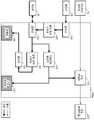
도 5는 일 실시예에 따른 전력 시스템의 전체 구성을 개략적으로 도시한다.5 schematically shows the overall configuration of a power system according to an embodiment.
도 5를 참조하면, 전력 시스템(1000)은 마더보드(100) 및 복수의 전력 모듈들(200_1~200_N)을 포함한다.Referring to FIG. 5, the
마더보드(100)는 마더보드 제어부(110), 전력 제어부(160) 및 구동전력 생성부(150)를 포함한다. 마더보드 제어부(110)는 통신 기능을 담당하는 통신부(115)를 포함할 수 있다.The
전력 모듈들(200_1~200_N)은 모듈 제어부(210_1~210_N), 전력 변환부(240_1~240_N), 전력 제어부(260_1~260_N), 및 구동전력 생성부(250_1~250_N)를 각각 포함한다. 모듈 제어부(210_1~210_N)는 통신부(215_1~215_N)를 각각 포함할 수 있다. 전력 모듈들(200_1~200_N), 모듈 제어부(210_1~210_N), 통신부(215_1~215_N), 전력 변환부(240_1~240_N), 전력 제어부(260_1~260_N), 및 구동전력 생성부(250_1~250_N)는 각각 전력 모듈(200), 모듈 제어부(210), 통신부(215), 전력 변환부(240), 전력 제어부(260) 및 구동전력 생성부(250)로 통칭될 수 있다.The power modules 200_1 to 200_N include module controllers 210_1 to 210_N, power converters 240_1 to 240_N, power controllers 260_1 to 260_N, and driving power generators 250_1 to 250_N, respectively. The module controllers 210_1 to 210_N may include communication units 215_1 to 215_N, respectively. Power modules 200_1 to 200_N, module control units 210_1 to 210_N, communication units 215_1 to 215_N, power conversion units 240_1 to 240_N, power control units 260_1 to 260_N, and driving power generation units 250_1 to 250_N ) May be collectively referred to as the
메인 전력은 마더보드(100)에 인가되어 전력 제어부(160)에 의해 제어될 수 있다. 구동전력 생성부(150)는 전력 제어부(160)를 통해 메인 전력을 공급받으면, 마더보드 제어부(110)를 구동하기 위한 구동전력을 생성할 수 있다.Main power is applied to the
전력 변환부(240)는 마더보드(100)의 전력 제어부(160)를 통해 메인 전력을 공급받으면, 미리 설정된 전압 레벨을 갖는 부하 전력을 생성하여 출력할 수 있다. 전력 제어부(260)는 전력 변환부(240)로부터 출력되는 부하 전력을 제어할 수 있다. 구동전력 생성부(250)는 마더보드(100)의 전력 제어부(160)를 통해 메인 전력을 공급받아, 모듈 제어부(210)를 구동하기 위한 구동전력을 생성할 수 있다. 예컨대, 구동전력은 3.3V의 전압 레벨을 가질 수 있다.When receiving main power through the
마더보드 제어부(110)의 통신부(115)는 모듈 제어부들(210)의 통신부들(215)과 통신할 수 있다. 도 5에 도시된 바와 같이, 마더보드 제어부(110)의 통신부(115)와 모듈 제어부들(210)의 통신부들(215)은 데이지-체인 방식으로 통신 가능하게 연결될 수 있다. 마지막으로 적층되는 전력 모듈 N(200_N)의 통신부(215_N)는 마더보드 제어부(110)의 통신부(115)와 직접 연결될 수 있다. 통신부(115, 215)는 마더보드 제어부(110)와 모듈 제어부(210) 각각에 포함되는 마이크로컨트롤러 유닛의 통신 기능을 의미할 수 있다. 마더보드 제어부(110)는 로봇 유닛의 메인 컨트롤러와 통신하기 위한 통신부를 더 포함할 수 있다.The
통신부(115)가 통신부들(215)과 통신하기 위하여, 전력 모듈들(200)이 마더보드(100) 상에 적층될 때 마다 통신부들(215)은 적층 순서에 따라 자동으로 ID가 부여될 수 있다. 이와 관련하여, 도 13 내지 도 15를 참조로 아래에서 더욱 자세히 설명한다.In order for the
도 6은 일 실시예에 따른 마더보드의 구성을 개략적으로 도시한다.6 schematically shows a configuration of a motherboard according to an embodiment.
도 5와 함께 도 6을 참조하면, 마더보드(100)는 마더보드 제어부(110), 전력핀(120), 구동전력 생성부(150), 및 전력 제어부(160)를 포함한다. 마더보드(100)는 배터리(30)와 연결될 수 있는 제1 입력단(102), 충전기(20)와 연결될 수 있는 제2 입력단(103)을 포함할 수 있다. 전력 제어부(160)는 방전 제어 스위치(161)와 충전 제어 스위치(162)를 포함할 수 있다. 마더보드(100)는 센서부(104)를 포함할 수 있다. 마더보드 제어부(110)는 로봇 장치의 메인 컨트롤러(10)와 통신할 수 있으며, 모듈 제어부들(210)과 통신할 수 있다. 도 6에 도시된 마더보드(100)는 예시적이며, 도 6에 도시된 구성요소들 중 적어도 일부만을 포함할 수도 있다.Referring to FIG. 6 along with FIG. 5, the
제1 입력단(102)은 배터리(30)의 단자에 연결되어 배터리(30)의 전력을 수신할 수 있다. 제2 입력단(103)은 충전기(20)의 단자에 연결되어, 충전 제어 스위치(162)를 통해 배터리(30)를 충전할 수 있다. 다른 예에 따르면, 배터리(30)는 충전 단자와 방전 단자를 별도로 가질 수 있으며, 배터리(30)의 방전 단자는 제1 입력단(102)에 연결되고, 배터리(30)의 충전 단자는 충전 제어 스위치(162)에 연결될 수도 있다.The
충전 제어 스위치(162)는 충전기(20)로부터 배터리(30)로의 충전을 제어하기 위한 스위치로서, 마더보드 제어부(110)에 의해 제어될 수 있다. 도 6에 도시되지는 않았지만, 마더보드 제어부(110)는 배터리(30)의 단자 전압을 감지할 수 있으며, 배터리(30)가 과충전되면, 충전 제어 스위치(162)를 턴 오프 시킬 수 있다. 충전 제어 스위치(162)는 전력 반도체 소자, FET, 또는 릴레이를 포함할 수 있다.The
전력핀(120)은 메인 전력을 공급하기 위한 단자이다. 충전기(20)가 제2 입력단(103)에 연결되는 경우, 메인 전력은 충전기(20)의 충전 전력일 수 있다. 충전기(20)가 제2 입력단(103)에 연결되지 않은 경우, 메인 전력은 배터리(30)에 저장된 배터리 전력일 수 있다. 이하에서 용이한 이해를 위하여, 메인 전력은 배터리(30)에 저장된 배터리 전력이라고 가정하여 설명한다.The
방전 제어 스위치(161)는 제1 입력단(102)과 전력핀(120) 사이에 연결되어, 전력 모듈들(200)에 배터리 전력의 공급 여부를 결정할 수 있다. 도 6에 도시되지는 않았지만, 마더보드 제어부(110)는 센서부(104)를 이용하여 전력핀(120)을 통해 출력되는 출력 전류를 감지할 수 있다. 센서부(104)는 출력 전류를 감지하기 위한 션트를 포함할 수 있다. 마더보드 제어부(110)는 센서부(104)를 이용하여 배터리 전력의 전압을 감지할 수 있다. 마더보드 제어부(110)는 배터리 전압이 과전압 또는 저전압일 때, 또는 과전류가 흐를 때, 방전 제어 스위치(161)를 턴 오프 시킬 수 있다. 다른 예로서, 로봇 장치가 사용자의 제어에 의해 턴 오프된 경우, 마더보드 제어부(110)는 방전 제어 스위치(161)를 턴 오프 시켜서 전력 모듈들(200)이 부하 전력을 생성하지 않도록 함으로써, 불필요한 전력 소비를 줄일 수 있다. 방전 제어 스위치(161)가 턴 온 되는 경우, 전력핀(120)에는 배터리 전력이 인가되며, 전력핀(120)을 통해 연결되는 전력 모듈들(200)에 배터리 전력이 공급될 수 있다. 방전 제어 스위치(161)는 전력 반도체 소자, FET, 또는 릴레이를 포함할 수 있다.The
구동전력 생성부(150)는 입력단(102)과 방전 제어 스위치(161) 사이에 연결될 수 있다. 구동전력 생성부(150)는 배터리 전력으로부터 구동전력을 생성하여 마더보드 제어부(110)에 공급할 수 있다. 구동전력 생성부(150)는 DC-DC 컨버터 회로를 포함할 수 있다. 구동전력 생성부(150)에 의해 생성되는 구동전력은 마더보드 제어부(110)를 구동하고 방전 및 충전 제어 스위치(161, 162)를 제어하기 위한 전압을 가질 수 있다. 구동전력의 전압은 마더보드 제어부(110)에 따라 예컨대 3.3V 또는 5V일 수 있다.The driving
마더보드 제어부(110)는 메인 컨트롤러(10)의 제어에 따라 전력 시스템(100)의 전체 동작을 제어할 수 있다. 예컨대, 마더보드 제어부(110)는 메인 컨트롤러(10)의 제어에 따라 방전 제어 스위치(161)를 턴 오프 시킬 수 있다. 또한, 마더보드 제어부(110)는 메인 컨트롤러(10)의 제어에 따라 모듈 제어부(210)에 제어 명령을 송신할 수도 있다. 마더보드 제어부(110)는 전력 시스템(100)의 상태, 예컨대, 각각의 전력 모듈들(200)의 동작 여부, 출력 전압 및 출력 전류 등에 관한 정보를 메인 컨트롤러(10)에 제공할 수 있다. 마더보드 제어부(110)는 모듈 제어부들(210)로부터 각각의 전력 모듈들(200)의 전력 변환부(240)의 동작 여부, 출력 제어 스위치(도 7의 261)의 개폐 상태, 출력 전압 및 출력 전류 등에 관한 정보를 수신할 수 있다.The
마더보드 제어부(110)는 배터리(30)의 단자 전압 및 충전 및 방전 전류, 각 전력 모듈들(200)의 전력 변환부(240)의 입력 전류, 출력 전류, 및 출력 전압에 관한 정보를 취득할 수 있다. 마더보드 제어부(110)는 기타 에러 신호들을 수신할 수도 있다.The
마더보드 제어부(110)는 전력 시스템(100)의 상태에 관한 정보들을 저장하기 위한 메모리(예컨대, EEPROM)를 포함할 수 있다. 메모리에는 위와 같은 정보가 로그 형태로 저장될 수 있다.The
따라서, 마더보드 제어부(110)는 각 전력 모듈들(200)의 동작 상태를 확인할 수 있으며, 필요 시 각 전력 모듈들(200)의 전원을 온/오프 제어할 수 있다. 또한, 배터리(도 6의 30)의 잔여 용량이 부족한 경우, 마더보드 제어부(110)는 필수적인 부하에만 부하 전력을 공급하고, 부가적인 부하에는 부하 전력을 공급하지 않도록 제어함으로써, 로봇 장치의 운영 효율을 높일 수 있다.Accordingly, the
도 6에 도시되지는 않았지만, 급격한 전류 및 전압 변화에 대비하여 마더보드(100)는 대용량 커패시터를 포함할 수 있다. 대용량 커패시터는 전력핀(120)과 접지 사이에 연결될 수 있다.Although not shown in FIG. 6, the
도 7은 일 실시예에 따른 전력 모듈의 구성을 개략적으로 도시한다.7 schematically shows a configuration of a power module according to an embodiment.
도 5와 함께 도 7을 참조하면, 전력 모듈(200)은 모듈 제어부(210), 관통 전력핀(220), 구동전력 생성부(250), 전력 변환부(240), 및 전력 제어부(260)를 포함한다. 전력 제어부(260)는 출력 제어 스위치(261)를 포함할 수 있다. 전력 모듈(200)은 출력단(204)을 포함할 수 있다. 전력 모듈(200)은 센서부(202) 및 퓨즈(203)를 포함할 수 있다. 모듈 제어부(210)는 마더보드 제어부(110) 및 다른 모듈 제어부들(210)과 통신할 수 있다. 도 7에 도시된 전력 모듈(200)은 예시적이며, 도 7에 도시된 구성요소들 중 적어도 일부만을 포함할 수도 있다.Referring to FIG. 7 along with FIG. 5, the
관통 전력핀(220)은 전력 모듈(200)이 마더보드(도 6의 100) 상에 적층될 때 전력핀(120)과 접촉하여, 배터리 전력을 수신할 수 있다. 관통 전력핀(220)은 전력핀(120)에 대응하는 위치에 배치될 수 있다. 구동전력 생성부(250)는 관통 전력핀(220)을 통해 공급되는 배터리 전력으로부터 구동전력을 생성하여 모듈 제어부(210)를 구동할 수 있다.The through
전력 변환부(240)는 배터리 전력으로부터 부하 전력을 생성하여 출력단(204)을 통해 부하에 공급할 수 있다. 전력 변환부(240)는 배터리 전력으로부터 변환하여 부하 전력을 생성하기 위한 DC-DC 컨버터 회로를 포함할 수 있다. 부하 전력은 전력 모듈(200)에 대해 설계된 바에 따라 미리 설정된 전압 레벨을 가질 수 있다. 예컨대, 부하 전력은 15V, 12V, 9V, 또는 5V의 전압 레벨을 가질 수 있다. 또한, 서로 다른 전력 모듈(200)의 전력 변환부들(240)은 동일한 전압 레벨을 갖더라도 서로 다른 허용 전류 크기를 가질 수도 있다. 모듈 제어부(210)는 전력 변환부(240)를 제어할 수 있으며, 제어 신호를 이용하여 전력 변환부(240)를 활성화 또는 비활성화 할 수 있다.The
출력 제어 스위치(261)는 전력 변환부(240)와 출력단(204) 사이에 배치되어, 전력 변환부(240)에서 생성되는 부하 전력을 제어할 수 있다. 출력 제어 스위치(261)는 모듈 제어부(210)에 의해 제어될 수 있다. 모듈 제어부(210)는 예컨대 센서부(202)를 통해 전력 변환부(240)의 출력 전압 및 출력 전류를 감지할 수 있다. 센서부(202)는 션트를 포함할 수 있다. 모듈 제어부(210)는 저전압, 과전압, 또는 과전류가 발생하는 경우, 출력 제어 스위치(261)를 턴 오프 시킴으로써, 출력단(204)에 연결되는 전기 부하들을 보호할 수 있다. 출력 제어 스위치(261)는 전력 반도체 소자, FET, 또는 릴레이를 포함할 수 있다.The
퓨즈(203)는 과전류가 발생할 경우 전력 변환부(240)와 출력단(204) 사이를 분리하여 출력단(204)에 연결되는 전기 부하들을 추가적으로 보호할 수 있다. 퓨즈(203)는 e-퓨즈일 수도 있으며, 퓨즈의 상태를 모듈 제어부(210)로 전송할 수 있다. 또한, 퓨즈(203)는 물리적 퓨즈일 수도 있으며, 모듈 제어부(210)는 아날로그-디지털 컨버터(ADC)를 이용하여 퓨즈(203)의 상태를 감지할 수 있다.When an overcurrent occurs, the
모듈 제어부(210)는 마더보드 제어부(110)의 제어 명령에 따라 전력 변환부(240)를 비활성화 또는 활성화시키거나, 출력 제어 스위치(261)를 턴 온 또는 턴 오프 시킬 수 있다. 모듈 제어부(210)는 전력 변환부(240)의 동작 여부, 출력 제어 스위치(261)의 개폐 상태, 출력 전압 및 출력 전류 등을 감지하여, 이들에 관한 정보를 마더보드 제어부(110)로 송신할 수 있다. 모듈 제어부(210)는 위의 정보들을 저장하기 위한 메모리(예컨대, EEPROM)를 포함할 수 있다. 메모리에는 로그 형태로 정보가 저장될 수 있다.The
모듈 제어부(210)는 전력 변환부(240)의 입력 전압, 입력 전류, 출력 전압 및 출력 전류, 및 출력단(204)의 전압에 관한 정보를 감지할 수 있다. 모듈 제어부(210)는 기타 에러 신호들을 수신할 수도 있다.The
도 7에 도시되지는 않았지만, 전력 모듈(200)은 정전기 방전(ESD)로부터 보호하기 위하여 TVS 다이오드를 포함할 수 있다. 또한, 전력 모듈(200)은 전력 변환부(240)를 보호하기 위하여 대용량 커패시터를 포함할 수도 있다. 대용량 커패시터는 전력 변환부(240)의 출력단에 연결될 수 있다.Although not shown in FIG. 7, the
도 8은 일 실시예에 따른 마더보드의 구성을 도시한다.8 shows a configuration of a motherboard according to an embodiment.
도 8을 참조하면, 도 8에 도시된 마더보드(100)는 마더보드 제어부(110)를 제외하고 도 6에 도시된 마더보드(100)와 실질적으로 동일하다. 마더보드 제어부(110)를 제외한 나머지 구성에 대하여 반복하여 설명하지 않는다. 마더보드 제어부(110)는 마더보드 MCU(111), 제1 핫스왑 컨트롤러(112) 및 제2 핫스왑 컨트롤러(113)를 포함할 수 있다. 마더보드 제어부(110)는 제1 핫스왑 컨트롤러(112)와 제2 핫스왑 컨트롤러(113) 중 하나만을 포함하거나, 제1 및 제2 핫스왑 컨트롤러(112, 113) 모두 포함하지 않을 수도 있다.Referring to FIG. 8, the
도 8에 도시된 실시예에 따르면, 제1 핫스왑 컨트롤러(112)는 방전 제어 스위치(161)를 제어할 수 있다. 제1 핫스왑 컨트롤러(112)는 센서부(104)로부터 배터리 전력의 전압 및 출력 전류를 감지하여, 과전압, 저전압 또는 과전류가 발생할 경우, 방전 제어 스위치(161)를 턴 오프 시킬 수 있다. 제1 핫스왑 컨트롤러(112)는 마더보드 MCU(111)와 통신할 수 있으며, 배터리 전력의 전압 및 출력 전류, 및 방전 제어 스위치(161)의 개폐 상태에 관한 정보를 마더보드 MCU(111)에 전송할 수 있다. 제1 핫스왑 컨트롤러(112)는 마더보드 MCU(111)의 제어에 따라 방전 제어 스위치(161)를 턴 온 또는 턴 오프 시킬 수 있다.According to the embodiment shown in FIG. 8, the first
제2 핫스왑 컨트롤러(113)는 충전 제어 스위치(162)를 제어할 수 있다. 제2 핫스왑 컨트롤러(113)는 충전기(20)가 제2 입력단(103)에 접속되었는지의 여부, 충전 전압 및 충전 전류 등을 감지하여, 과전압, 저전압 또는 과전류가 발생할 경우, 충전 제어 스위치(162)를 턴 오프 시킬 수 있다. 제2 핫스왑 컨트롤러(113)는 마더보드 MCU(111)와 통신할 수 있으며, 충전기(20)의 연결 상태, 충전 전압 및 충전 전류, 및 충전 제어 스위치(162)의 개폐 상태에 관한 정보를 마더보드 MCU(111)에 전송할 수 있다. 제2 핫스왑 컨트롤러(113)는 마더보드 MCU(111)의 제어에 따라 충전 제어 스위치(162)를 턴 온 또는 턴 오프 시킬 수 있다.The second
마더보드 MCU(111)는 제1 및 제2 핫스왑 컨트롤러(112, 113)로부터 수신된 정보들을 메인 컨트롤러(10)로 전송할 수 있다.The
도 9는 일 실시예에 따른 전력 모듈의 구성을 도시한다.9 shows a configuration of a power module according to an embodiment.
도 9를 참조하면, 도 9에 도시된 전력 모듈(200)은 모듈 제어부(210)를 제외하고 도 7에 도시된 전력 모듈(200)과 실질적으로 동일하다. 모듈 제어부(210)를 제외한 나머지 구성에 대하여 반복하여 설명하지 않는다. 모듈 제어부(210)는 모듈 MCU(211), 및 핫스왑 컨트롤러(212)를 포함할 수 있다. 모듈 제어부(210)는 핫스왑 컨트롤러(212)를 포함하지 않을 수도 있다.Referring to FIG. 9, the
도 9에 도시된 실시예에 따르면, 핫스왑 컨트롤러(212)는 출력 제어 스위치(261)를 제어할 수 있다. 핫스왑 컨트롤러(212)는 센서부(202)로부터 부하 전력의 전압 및 출력 전류를 감지하여, 과전압, 저전압 또는 과전류가 발생할 경우, 출력 제어 스위치(261)를 턴 오프 시킬 수 있다. 핫스왑 컨트롤러(212)는 모듈 MCU(211)와 통신할 수 있으며, 부하 전력의 전압 및 출력 전류, 및 출력 제어 스위치(261)의 개폐 상태에 관한 정보를 모듈 MCU(211)에 전송할 수 있다. 핫스왑 컨트롤러(212)는 모듈 MCU(211)의 제어에 따라 출력 제어 스위치(261)를 턴 온 또는 턴 오프 시킬 수 있다. 모듈 MCU(211)는 핫스왑 컨트롤러(212)로부터 수신된 정보들을 마더보드 MCU(111)로 전송할 수 있다.According to the embodiment shown in FIG. 9, the
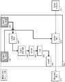
도 10은 다른 실시예에 따른 전력 시스템의 전체 구성을 개략적으로 도시한다.10 schematically shows the overall configuration of a power system according to another embodiment.
도 10을 참조하면, 전력 시스템(1000a)은 마더보드(100a) 및 복수의 전력 모듈들(200_1a~200_Na)을 포함한다.Referring to FIG. 10, the
마더보드(100a)는 마더보드 제어부(110), 전력 제어부(160) 및 구동전력 생성부(150)를 포함한다. 전력 모듈들(200_1a~200_Na)은 모듈 제어부(210_1~210_N), 전력 변환부(240_1~240_N), 및 전력 제어부(260_1~260_N)를 각각 포함한다.The
전력 시스템(1000a)은 복수의 전력 모듈들(200_1a~200_Na)이 구동전력 생성부들(도 5의 250_1~250_N)을 포함하지 않는다는 점을 제외하고 도 5에 도시된 전력 시스템(1000)과 실질적으로 동일하다. 동일한 부분에 대하여 반복하여 설명하지 않는다. 복수의 전력 모듈들(200_1a~200_Na)은 전력 모듈들(200a)로 통칭될 수 있다.The
도 10의 실시예에 따르면, 전력 모듈들(200a) 각각의 모듈 제어부들(210)은 마더보드(100a)의 구동전력 생성부(150)에 의해 생성되는 구동전력에 의해 구동될 수 있다. 구동전력 생성부(150)에 의해 출력되는 구동전력은 마더보드(100a)의 제1 타입의 핀(120) 중 적어도 하나, 및 전력 모듈들(200a)의 관통핀(220) 중 적어도 하나를 통해 모듈 제어부들(210)에 공급될 수 있다. 제1 타입의 핀들(120) 중에서 구동전력을 전달하는 핀은 구동 전력핀(도 11의 121)으로 지칭되고, 관통핀들(220) 중에서 구동 전력핀(121)과 접촉하도록 동일한 위치에 배치되는 핀은 제2 관통핀(도 12의 221)로 지칭된다. 본 실시예에서 배터리 전력을 전달하는 관통핀은 제1 관통핀(도 12의 220)으로 지칭한다. 구동 전력핀(121) 및 제2 관통핀(221)은 각각 복수의 핀들로 구성될 수 있다.According to the embodiment of FIG. 10, the
도 11은 다른 실시예에 따른 마더보드의 구성을 개략적으로 도시한다.11 schematically shows a configuration of a motherboard according to another embodiment.
도 10과 함께 도 11을 참조하면, 마더보드(100a)는 마더보드 제어부(110), 전력핀(120), 구동 전력핀(121), 구동전력 생성부(150), 및 전력 제어부(160)를 포함한다. 마더보드(100a)는 도 6에 도시된 마더보드(100)와 비교할 때 구동 전력핀(121)을 더 포함한다는 점을 제외하고 실질적으로 동일하다. 동일한 구성요소들에 대하여 반복하여 설명하지 않는다.Referring to FIG. 11 along with FIG. 10, the
구동전력 생성부(150)는 배터리 전력으로부터 모듈 제어부(210)를 구동하기 위한 구동전력을 생성할 수 있다. 구동전력 생성부(150)에서 생성된 구동전력은 모듈 제어부(210)에 공급될 뿐만 아니라, 구동 전력핀(121)에 인가될 수 있다.The driving
구동 전력핀(121)은 구동전력 생성부(150)에서 생성된 구동전력을 전력 모듈들(도 10의 200a)에게 전달할 수 있다.The driving
도 11에 도시되지는 않았지만, 구동전력 생성부(150)와 구동 전력핀(121) 사이에 마더보드 제어부(110)에 의해 제어되는 스위치가 배치될 수 있다. 마더보드 제어부(110)는 스위치를 제어함으로써, 전력 모듈들(200a)을 활성화하거나 비활성화시킬 수 있다. 예컨대, 마더보드 제어부(110)가 스위치를 턴 오프 시켜서, 구동 전력핀(1210에 구동전력이 인가되지 않게 하면, 마더보드(100a) 상에 적층된 전력 모듈들(200a)의 모듈 제어부들(210)에는 구동 전력이 공급되지 않는다. 유휴 상태일 때, 모듈 제어부들(210)을 완전히 비활성화시킴으로써, 전력 소모를 더욱 감소시킬 수 있다.Although not shown in FIG. 11, a switch controlled by the
마더보드 제어부(110)는 스위치를 턴 온 시켜서, 모듈 제어부들(210)에 구동 전력을 공급할 수 있다. 모듈 제어부들(210)은 구동 전력이 제공됨에 따라서 웨이크 업 할 수 있다. 마더보드 제어부(101)는 핫스왑 컨트롤러를 포함할 수 있으며, 핫스왑 컨트롤러에 의해 스위치가 제어될 수 있다.The
도 11에 도시되지는 않았지만, 구동전력 생성부(150)와 구동 전력핀(121) 사이에 센서부가 배치될 수 있으며, 센서부는 구동 전력핀(121)을 통해 출력되는 구동 전력의 전압 및 전류를 감지할 수 있다. 센서부에서 감지된 값들은 모듈 제어부(210)에 제공될 수 있다.Although not shown in FIG. 11, a sensor unit may be disposed between the driving
도 12는 다른 실시예에 따른 전력 모듈의 구성을 개략적으로 도시한다.12 schematically shows a configuration of a power module according to another embodiment.
도 10과 함께 도 12를 참조하면, 전력 모듈(200a)은 모듈 제어부(210), 제1 관통핀(220), 제2 관통핀(221), 전력 변환부(240), 및 전력 제어부(260)를 포함한다. 전력 모듈(200a)은 도 7에 도시된 전력 모듈(200)과 비교할 때 제2 관통핀(221)을 더 포함하고, 구동전력 생성부(250)를 포함하지 않는다는 점을 제외하고 실질적으로 동일하다. 동일한 구성요소들에 대하여 반복하여 설명하지 않는다.Referring to FIG. 12 along with FIG. 10, the
제2 관통핀(221)은 도 11의 구동 전력핀(121)에 대응되는 위치에 배치되어, 전력 모듈(200a)이 마더보드(100a) 상에 적층되면, 제2 관통핀(221)은 구동 전력핀(121)과 접촉한다. 그에 따라, 제2 관통핀(221)에도 마더보드(100a)의 구동전력 생성부(150)에서 생성된 구동전력이 인가된다.The second through
제2 관통핀(221)은 모듈 제어부(210)에 연결되며, 모듈 제어부(210)는 제2 관통핀(221)을 통해 구동전력을 제공받을 수 있다. 모듈 제어부(210)는 제2 관통핀(221)을 통해 마더보드(100a)로부터 구동전력을 공급받으므로, 별도로 구동전력 생성부를 포함하지 않을 수 있다.The second through
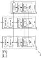
도 13은 일 실시예에 따라서 마더보드와 전력 모듈들 간의 데이터 통신을 수행하기 위한 구성도를 도시한다.13 illustrates a configuration diagram for performing data communication between a motherboard and power modules according to an embodiment.
도 13을 참조하면, 예시적으로 도 8를 참조로 설명된 마더보드 MCU(111)와 도 9를 참조로 설명된 모듈 MCU들(211_1~211_N)가 SPI 데이지-체인 방식으로 연결되어 서로 통신하는 구성이 도시된다. 이때, 마더보드 MCU(111)는 SPI 마스터로 동작하고, 모듈 MCU들(211_1~211_N)은 SPI 슬레이브로 동작할 수 있다.Referring to FIG. 13, by way of example, the
도 13에 도시된 연결 구성은 예시적이며, 다른 연결 구성을 가지고 다른 통신 방식이 사용될 수도 있다. 예컨대, 이더캣(EtherCAT) 방식이 사용될 수도 있다. 이 경우, 마더보드 MCU(111)는 이더캣 마스터로 동작하고, 모듈 MCU들(211_1~211_N)은 이더캣 슬레이브로 동작할 수 있다.The connection configuration shown in FIG. 13 is exemplary, and different communication methods may be used with different connection configurations. For example, the EtherCAT method may be used. In this case, the
다른 예로서, 로봇 장치의 메인 컨트롤러가 마스터로 동작하고, 마더보드 MCU(111)와 모듈 MCU들(211_1~211_N)이 모두 슬레이브로 동작할 수도 있다.As another example, the main controller of the robot device may operate as a master, and both the
본 실시예에 따르면, 마더보드 MCU(111)는 클럭 단자(SCK), 칩 선택 단자(CSb), 데이터 출력 단자(MOSI) 및 데이터 입력 단자(MISO)를 가질 수 있다. 모듈 MCU들(211_1~211_N) 각각도 역시 클럭 단자(SCK), 칩 선택 단자(CSb), 데이터 입력 단자(DI), 및 데이터 출력 단자(DOUT) 및 를 가질 수 있다.According to the present embodiment, the
마더보드 MCU(111)의 클럭 단자(SCK)는 모듈 MCU들(211_1~211_N)의 클럭 단자들(SCK)과 병렬로 연결된다. 마더보드 MCU(111)의 클럭 단자(SCK)로부터 출력된 클럭 신호(SCK)는 모듈 MCU들(211_1~211_N)에 동시에 입력된다.The clock terminal SCK of the
마더보드 MCU(111)의 칩 선택 단자(CSb)는 모듈 MCU들(211_1~211_N)의 칩 선택 단자들(CSb)과 병렬로 연결된다. 마더보드 MCU(111)의 칩 선택 단자(CSb)로부터 칩 선택 신호(SCb)는 모듈 MCU들(211_1~211_N)에 동시에 입력된다.The chip select terminals CSb of the
마더보드 MCU(111)의 클럭 단자(SCK) 및 칩 선택 단자(CSb)는 제1 타입의 핀(도 1의 120)에 연결되고, 모듈 MCU들(211_1~211_N)의 클럭 단자들(SCK) 및 칩 선택 단자들(CSb)는 관통핀(도 1의 220)에 연결될 수 있다. 모듈 MCU들(211_1~211_N)의 클럭 단자들(SCK) 및 칩 선택 단자들(CSb)에 연결되는 관통핀은 관통 통신핀으로 지칭될 수 있다.The clock terminal SCK and the chip select terminal CSb of the
마더보드 MCU(111)의 데이터 출력 단자(MOSI)는 제1 모듈 MCU(211_1)의 데이터 입력 단자(DI)에 연결되고, 제1 모듈 MCU(211_1)의 데이터 출력 단자(DOUT)은 제2 모듈 MCU(211_2)의 데이터 입력 단자(DI)에 연결된다. 이러한 방식으로 데이터 출력 단자들(DOUT)은 다음 모듈 MCU(211)의 데이터 입력 단자(DI)에 연결된다. 마지막에 위치하는 제N 모듈 MCU(211_N)의 데이터 출력 단자(DOUT)는 마더보드 MCU(111)의 데이터 입력 단자(MISO)에 연결된다.The data output terminal (MOSI) of the
마더보드 MCU(111)의 데이터 출력 단자(MOSI)로부터 출력된 데이터 신호는 제1 모듈 MCU(211_1)로부터 제N 모듈 MCU(211_N)까지 클럭 신호(SCK)에 동기화하여 순차적으로 전송된다. 제1 모듈 MCU(211_1)로부터 출력되는 데이터 신호 역시 제2 내지 제N 모듈 MCU(211_2~211_N)를 거쳐서 마더보드 MCU(111)에 입력된다.The data signal output from the data output terminal MOSI of the
마더보드 MCU(111)의 데이터 출력 단자(MOSI)는 제2 타입의 핀(도 1의 130)에 연결될 수 있다.The data output terminal MOSI of the
모듈 MCU들(211_1~211_N)의 데이터 입력 단자들(DI)은 하부핀(도 1의 230b)에 연결되고, 모듈 MCU들(211_1~211_N)의 데이터 출력 단자들(DOUT)은 상부핀(도 1의 230t)에 연결될 수 있다. 모듈 MCU들(211_1~211_N)의 데이터 입력 단자들(DI)에 연결되는 하부핀(230b)은 하부 통신핀으로 지칭되고, 모듈 MCU들(211_1~211_N)의 데이터 출력 단자들(DOUT)에 연결되는 상부핀(230t)은 상부 통신핀으로 지칭될 수 있다.The data input terminals DI of the module MCUs 211_1 to 211_N are connected to the lower pin (230b in FIG. 1), and the data output terminals DOUT of the module MCUs 211_1 to 211_N are upper pins (Fig. 1, can be connected to 230t). The
전력 모듈들(200_1~200_N)은 모두 마지막으로 적층될 수 있으므로, 모듈 MCU들(211_1~211_N)의 데이터 출력 단자들(DOUT)은 관통핀(도 1의 220) 및 제1 타입의 핀(120)을 통해 마더보드 MCU(111)의 데이터 입력 단자(MISO)에도 연결될 수 있다. 모듈 MCU들(211_1~211_N)의 데이터 출력 단자들(DOUT)에 연결되는 관통핀(도 1의 220)도 관통 통신핀으로 지칭될 수 있다. 모듈 MCU들(211_1~211_N)의 데이터 출력 단자들(DOUT)에 대하여 도 17을 참조하여 아래에서 더욱 자세히 설명한다.Since all of the power modules 200_1 to 200_N may be stacked last, the data output terminals DOUT of the module MCUs 211_1 to 211_N are through pins (220 in FIG. 1) and a first type of pin 120 ) Can also be connected to the data input terminal (MISO) of the
도 14는 일 실시예에 따라서 전력 모듈이 적층 순서에 해당하는 ID를 자동으로 할당하는 방법을 설명하기 위한 예시적인 도면이다14 is an exemplary diagram for explaining a method of automatically allocating an ID corresponding to a stacking order by a power module according to an embodiment
도 14를 참조하면, 마더보드 MCU(111)는 칩 선택 신호(CSb)를 인에이블 상태로 천이할 수 있다. 도 14에 도시된 바와 같이, 미리 설정된 개수, 예컨대 16개의 사이클 단위 클럭 신호(SCK)에 응답하여, 모듈 MCU(211_1~211_N)는 다음 모듈 MCU(211_2~211_N)로 데이터 신호를 전달할 수 있다. 이하에서는 데이터 신호를 다음 모듈 MCU(211_2~211_N)로 전달하는 시간 기준인 16개의 사이클 단위 클럭 신호(SCK)를 단위 클럭 신호라고 지칭한다.Referring to FIG. 14, the
마더보드 MCU(111)는 칩 선택 신호(CSb)를 인에이블 상태로 천이한 후 첫 번째 단위 클럭 신호에 동기화하여 미리 설정된 헤더 데이터 신호(HEADER)를 출력할 수 있다.The
제1 모듈 MCU(211_1)는 첫 번째 단위 클럭 신호에 동기화하여 헤더 데이터 신호(HEADER)를 수신할 수 있다. 제1 모듈 MCU(211_1)는 인에이블 상태의 칩 선택 신호(CSb)에 의해 활성화된 후 헤더 데이터 신호가 바로 수신되었으므로, 제1 모듈 MCU(211_1)는 자신이 첫 번째로 적층되었음을 결정하고 적층 순서에 대응하는 ID로 1을 스스로 할당할 수 있다. 제1 모듈 MCU(211_1)는 두 번째 단위 클럭 신호에 동기화하여 헤더(HEADER) 데이터 신호를 제2 모듈 MCU(211_2)로 출력할 수 있다.The first module MCU 211_1 may receive the header data signal HEADER in synchronization with the first unit clock signal. Since the first module MCU 211_1 has received the header data signal immediately after being activated by the enabled chip select signal CSb, the first module MCU 211_1 determines that it has been stacked first and stacking order 1 can be assigned by itself as the ID corresponding to. The first module MCU 211_1 may output a header data signal to the second module MCU 211_2 by synchronizing with the second unit clock signal.
제2 모듈 MCU(211_2)는 두 번째 단위 클럭 신호에 동기화하여 헤더 데이터 신호(HEADER)를 수신할 수 있다. 제2 모듈 MCU(211_2)는 인에이블 상태의 칩 선택 신호(CSb)에 의해 활성화된 후 두 번째 단위 클럭 신호에 동기화하여 헤더 데이터 신호(HEADER)를 수신하였으므로, 제2 모듈 MCU(211_2)는 자신이 두 번째로 적층되었음을 감지할 수 있다. 제2 모듈 MCU(211_2)는 자신의 적층 순서에 대응하여 ID를 2로 할당할 수 있다.The second module MCU 211_2 may receive the header data signal HEADER by synchronizing with the second unit clock signal. The second module MCU 211_2 receives the header data signal HEADER by synchronizing with the second unit clock signal after being activated by the chip select signal CSb in the enabled state, so the second module MCU 211_2 It can be detected that this is the second stacking. The second module MCU 211_2 may allocate an ID of 2 according to its stacking order.
이러한 방식으로 각각의 모듈 MCU들(211_3~211_N)은 인에이블 상태의 칩 선택 신호를 수신한 시점과 미리 설정된 헤더 데이터 신호(HEADER)를 수신한 시점 사이에 몇 사이클의 클럭 신호가 수신되었는지를 카운트함으로써 자신의 적층 순서를 감지할 수 있으며, 자신의 적층 순서에 해당하는 ID를 스스로 할당할 수 있다.In this way, each module MCU (211_3 to 211_N) counts the number of cycles of the clock signal received between the time when the chip select signal in the enabled state is received and the time when the preset header data signal (HEADER) is received. By doing so, you can detect your own stacking order, and you can assign an ID corresponding to your stacking order by yourself.
모듈 MCU들(211_1~211_N)은 자신에게 할당된 ID와 함께 자신의 출력 전압 등의 상태 정보를 마더보드 MCU(111)로 송신할 수 있다.The module MCUs 211_1 to 211_N may transmit status information, such as their output voltage, to the
헤더 데이터 신호(HEADER)가 한 바퀴 순환하여, 마더보드 MCU(111)가 다시 헤더 데이터 신호(HEADER)를 수신하면, 마더보드 MCU(111)는 자신이 헤더 데이터 신호(HEADER)를 송신한 시점과 다시 헤더 데이터 신호(HEADER)를 수신한 시점의 차이를 기초로 N개의 전력 모듈들(200)이 마더보드(100) 상에 적층되었다는 것을 파악할 수 있다. 마더보드 MCU(111)는 0x000N의 ID를 갖는 제N 모듈 MCU(211_N)가 마지막으로 적층된 전력 모듈(200)이라는 정보를 제공할 수 있다.When the header data signal (HEADER) circulates once, and the
도 15는 다른 실시예에 따라서 전력 모듈이 적층 순서에 해당하는 ID를 자동으로 할당하는 방법을 설명하기 위한 예시적인 도면이다15 is an exemplary diagram illustrating a method of automatically allocating an ID corresponding to a stacking order by a power module according to another embodiment
도 15를 참조하면, 마더보드 MCU(111)는 아이디 설정 명령(ID COM)과 함께 예컨대, 0x0000이라는 데이터를 제1 모듈 MCU(211_1)로 전송할 수 있다. 도 15에 도시된 바와 같이, 마더보드 MCU(111)는 연속하는 단위 클럭 신호 중에서 첫 번째 단위 클럭 신호에 동기화하여 아이디 설정 명령(ID COM)를 송신하고 그 다음 단위 클럭 신호에 동기화하여 0x0000이라는 데이터를 송신할 수 있다.Referring to FIG. 15, the
제1 모듈 MCU(211_1)는 아이디 설정 명령(ID COM) 이후에 수신되는 0x0000이라는 데이터를 통해, 자신의 아래에 0x0000의 ID를 갖는 마더보드(100)가 배치되어 있음을 감지할 수 있다. 제1 모듈 MCU(211_1)는 마더보드(100) 상에 첫 번째로 적층된 것이므로, 0x0001의 ID를 스스로 할당할 수 있다. 제1 모듈 MCU(211_1)는 아이디 설정 명령(ID COM)과 자신의 ID 데이터(즉, 0x0001)를 제2 모듈 MCU(211_2)에게 송신할 수 있다.The first module MCU 211_1 may detect that the
이러한 방식으로 각각의 모듈 MCU(211_2~211_N)는 자신의 적층 순서를 파악할 수 있고, 자신의 적층 순서에 해당하는 ID를 스스로 할당할 수 있다.In this way, each module MCU 211_2 to 211_N can determine its own stacking order, and can allocate an ID corresponding to its stacking order by itself.
아이디 설정 명령(ID COM)이 한 바퀴 순환하여, 마더보드 MCU(111)가 다시 아이디 설정 명령(ID COM)과 ID 데이터(예컨대, 도 15의 예에서 0x0004)를 수신하면, 마더보드 MCU(111)는 ID 데이터로부터 4개의 전력 모듈들(200)이 마더보드(100) 상에 적층되었다는 것을 파악할 수 있다. 마더보드 MCU(111)는 0x0004의 ID를 갖는 제4 모듈 MCU(211_4)가 마지막으로 적층된 전력 모듈(200)이라는 정보를 제공할 수 있다.When the ID setting command (ID COM) circulates once and the
도 16은 일 실시예에 따라서 전력 모듈이 마지막으로 적층되었음을 감지하기 위한 구성을 개략적으로 도시한다.16 schematically shows a configuration for detecting that a power module is last stacked according to an embodiment.
도 16을 참조하면, 전력 모듈들(200a, 200b)은 하부 기능핀(231a, 231b), 및 상부 기능핀(232a, 232b)을 각각 포함할 수 있다. 하부 기능핀(231a, 231b)과 상부 기능핀(232a, 232b)은 적층될 때 서로 접촉하도록 대응되는 위치에 배치될 수 있다.Referring to FIG. 16, the
하부 기능핀(231a, 231b)은 모듈 기판(201)의 하부 표면에 배치되고, 제1 전압이 인가될 수 있다. 도 16에 도시된 바와 같이, 제1 전압은 예시적으로 접지 전압일 수 있다. 상부 기능핀(232a, 232b)은 모듈 기판(201)의 상부 표면에 배치되고, 저항을 통해 제2 전압이 인가될 수 있다. 도 16에 도시된 바와 같이 제2 전압은 예시적으로 Vcc 전압일 수 있다. 상부 기능핀(232a, 232b)은 모듈 MCU(211a, 211b)의 기능 단자에 연결될 수 있다. 모듈 MCU(211a, 211b)은 기능 단자에서 감지되는 전압을 기초로 자신의 전력 모듈(200a, 200b)이 마지막으로 적층된 전력 모듈인지의 여부를 감지할 수 있다.The
하부 전력 모듈(200a)의 경우, 상부 전력 모듈(200b)이 상부에 적층되므로, 상부 기능핀(232a)은 하부 기능핀(231b)와 접촉하게 된다. 하부 전력 모듈(200a)의 MCU(211a)는 상부 기능핀(232a)와 연결된 기능 단자에서 제1 전압을 감지할 것이다. 상부 기능핀(232a)은 제1 전압이 인가되는 하부 기능핀(231b)와 직접 접촉하기 때문이다.In the case of the
반면에, 상부 전력 모듈(200b)의 경우, 가장 마지막으로 적층되므로, 상부 기능핀(232b)은 다른 핀들과 접촉하지 않는다. 상부 전력 모듈(200b)의 MCU(211b)는 상부 기능핀(232b)와 연결된 기능 단자에서 제2 전압을 감지할 것이다. 따라서, MCU들(211a, 211b)은 기능 단자에서 감지되는 전압이 제1 전압인지 아니면 제2 전압인지의 여부에 따라 자신의 전력 모듈(200a, 200b)이 마지막으로 적층된 전력 모듈인지를 판단할 수 있다.On the other hand, in the case of the
도 17은 일 실시예에 따라서 모듈 MCU의 데이터 출력 단자의 구성을 개략적으로 도시한다.17 schematically shows a configuration of a data output terminal of a module MCU according to an embodiment.
도 17을 참조하면, 모듈 MCU(211)는 디먹스(217)을 포함할 수 있다. 디먹스(217)의 입력 단자(IN)는 모듈 MCU(211)의 데이터 출력 단자(DOUT)에 연결되고, 제1 출력 단자(OUT1)는 상부 통신핀(230t)에 연결되고, 제2 출력 단자(OUT2)는 마더보드 MCU(111)의 데이터 입력 단자(MISO)에 연결되도록 배치되는 관통 통신핀에 연결될 수 있다.Referring to FIG. 17, the
디먹스(217)는 입력 단자(IN)를 제1 출력 단자(OUT1) 또는 제2 출력 단자(OUT2) 중 하나에 연결하기 위한 선택 신호가 입력되는 선택 단자(sel)를 포함할 수 있다.The
모듈 MCU(211)는 예컨대 도 16의 실시예에서 설명한 방법에 따라 자신이 마지막으로 적층된 전력 모듈(200)이면, 입력 단자(IN)를 제2 출력 단자(OUT2)에 연결하기 위한 제1 레벨의 선택 신호를 출력할 수 있다. 모듈 MCU(211)는 자신이 마지막으로 적층된 전력 모듈(200)이 아니라면, 입력 단자(IN)를 제1 출력 단자(OUT1)에 연결하기 위한 제2 레벨의 선택 신호를 출력할 수 있다.The
이와 같이 전력 모듈들(200)은 자신이 마지막으로 적층될 수 있고 그렇지 않을 수도 있지만, 어떠한 경우에도 도 13에 도시된 바와 같이 연결 구성을 가질 수 있다.In this way, the
도 18은 또 다른 실시예에 따른 전력 시스템을 개략적으로 도시한다.18 schematically shows a power system according to another embodiment.
도 18을 참조하면, 전력 시스템(1000b)은 도 1의 전력 시스템(1000)과 비교할 때, 전력 모듈들(200) 각각이 출력단(204)을 더 포함하고, 부하 공유 모듈(300)을 더 포함한다는 점을 제외하고는 실질적으로 동일하다.Referring to FIG. 18, when compared to the
부하 공유 모듈(300)은 연속적으로 적층되고 동일 레벨의 출력 전압을 출력하는 적어도 2개의 전력 모듈들(예컨대, 200a, 200b) 각각의 출력단(204)에 수평으로 결합할 수 있다.The
부하 공유 모듈(300)은 기판(301), 기판(301)의 제1 면에 배치되는 제1 입력단(302)와 제2 입력단(303), 및 기판(301)의 제2 면에 배치되는 출력단(304)을 포함할 수 있다. 제1 입력단(302)은 연속으로 적층되는 전력 모듈 중 하나(예컨대, 200a)의 출력단(204)와 결합되고, 제2 입력단(303)은 연속으로 적층되는 전력 모듈 중 다른 하나(예컨대, 200b)의 출력단(204)에 결합될 수 있다.The
출력단(304)은 출력단(204)과 동일한 크기와 형상을 가질 수 있다. 도 18에 도시되지는 않았지만, 제1 입력단(302)과 출력단(304) 사이에 다이오드가 연결되고, 제2 입력단(302)과 출력단(304) 사이에도 다이오드가 연결될 수 있다.The
예컨대, 제1 전력 모듈(200a)가 15V를 출력하지만, 허용 전류가 10A일 수 있다. 제2 전력 모듈(200b)도 15V를 출력하지만, 허용 전류가 10A일 수 있다. 그러나, 로봇 장치는 15V의 전압 및 15A의 전류가 공급되어야 하는 부하가 탑재될 수 있다. 이 경우, 제1 전력 모듈(200a)과 제2 전력 모듈(200b) 모두 부하가 필요로 하는 부하 전력을 공급할 수 없다. 그러나, 본 발명에 따라 부하 공유 모듈(300)을 통해 제1 전력 모듈(200a)에서 생성한 부하 전력과 제2 전력 모듈(200b)에서 생성한 부하 전력은 공유되어 많은 전류를 필요로 하는 부하에 공급될 수 있다. 따라서, 더욱 효율적인 전력 분배가 가능하며, 부하가 많은 전력을 필요로 하더라도 이에 대응하여 많은 부하 전력을 제공할 수 있다. 게다가, 적층 구조를 갖는 전력 시스템(1000)에 측면으로 결합되므로 차지하는 부피도 작다.For example, although the
도 18의 실시예에 따르면, 전력 시스템(1000)의 전력 모듈들(200)은 동일한 간격으로 적층될 수 있다.According to the embodiment of FIG. 18, the
이상에서 본 발명이 구체적인 구성요소 등과 같은 특정 사항과 한정된 실시예 및 도면에 의하여 설명되었으나, 이는 본 발명의 보다 전반적인 이해를 돕기 위하여 제공된 것일 뿐, 본 발명이 상기 실시예에 한정되는 것은 아니며, 본 발명이 속하는 기술분야에서 통상적인 지식을 가진 자라면 이러한 기재로부터 다양한 수정과 변경을 꾀할 수 있다.In the above, the present invention has been described by specific matters such as specific elements and limited embodiments and drawings, but this is provided only to help a more general understanding of the present invention, and the present invention is not limited to the above embodiments. Anyone with ordinary knowledge in the technical field to which the invention belongs can make various modifications and changes from these descriptions.
따라서, 본 발명의 사상은 상기 설명된 실시예에 국한되어 정해져서는 아니 되며, 후술하는 특허청구범위뿐만 아니라 이 특허청구범위와 균등한 또는 이로부터 등가적으로 변경된 모든 범위는 본 발명의 사상의 범주에 속한다고 할 것이다.Accordingly, the spirit of the present invention is limited to the above-described embodiments and should not be defined, and all ranges equivalent to or equivalently changed from the claims to be described later as well as the claims to be described later are the scope of the spirit of the present invention. It will be said to belong to.
Claims (23)
Translated fromKorean상기 마더보드 상에 순차적으로 적층될 수 있는 복수의 전력 모듈을 포함하며,
상기 복수의 전력 모듈 각각은,
모듈 기판;
상기 마더보드 상에 적층되면 상기 전력핀에 연결되고 상기 모듈 기판을 관통하는 관통 전력핀;
상기 관통 전력핀을 통해 공급되는 상기 메인 전력을 각 전력 모듈에 대해 미리 설정된 전력으로 변환하여 출력하는 전력 변환부;
모듈 제어부;
상기 모듈 기판을 관통하는 제1 내지 제3 관통 통신핀;
상기 모듈 기판의 저면에 배치되고, 상기 모듈 제어부의 데이터 입력 단자에 연결되는 하부 통신핀; 및
상기 모듈 기판의 상면에 상기 하부 통신핀에 대응하도록 배치되, 상기 모듈 제어부의 데이터 출력 단자에 연결되는 상부 통신핀을 포함하고,
상기 제1 관통 통신핀은 상기 마더보드 제어부로부터 출력되는 클럭 신호를 전달하고,
상기 제2 관통 통신핀은 상기 마더보드 제어부로부터 출력되는 칩 선택 신호를 전달하고,
상기 마더보드 제어부로부터 송신된 데이터는 상기 복수의 전력 모듈들 각각의 상기 하부 통신핀 및 상기 상부 통신핀을 통해 상기 복수의 모듈 제어부에게 전송되고, 상기 마더보드 상에 마지막으로 적층된 전력 모듈의 모듈 제어부로부터 출력되는 데이터는 상기 제3 관통 통신핀을 통해 상기 마더보드 제어부로 전달되는 것을 특징으로 하는 전력 시스템.A motherboard including a motherboard substrate, a motherboard controller, and a power pin on the motherboard substrate, and supplying main power through the power pins; And
It includes a plurality of power modules that can be sequentially stacked on the motherboard,
Each of the plurality of power modules,
Module substrate;
A through power pin connected to the power pin when stacked on the motherboard and passing through the module substrate;
A power converter configured to convert the main power supplied through the through power pin into power preset for each power module and output the converted power;
Module control unit;
First to third through communication pins penetrating the module substrate;
A lower communication pin disposed on the bottom of the module substrate and connected to a data input terminal of the module control unit; And
And an upper communication pin disposed on an upper surface of the module substrate to correspond to the lower communication pin and connected to a data output terminal of the module control unit,
The first through communication pin transmits a clock signal output from the motherboard control unit,
The second through communication pin transmits a chip selection signal output from the motherboard control unit,
The data transmitted from the motherboard control unit is transmitted to the plurality of module control units through the lower communication pin and the upper communication pin of each of the plurality of power modules, and the power module module finally stacked on the motherboard Data output from the control unit is transmitted to the motherboard control unit through the third through communication pin.
상기 복수의 전력 모듈들 각각의 상기 모듈 제어부는 상기 칩 선택 신호를 수신한 제1 시점과 미리 설정된 헤더 데이터를 수신한 제2 시점 사이에 수신되는 상기 클럭 신호의 개수를 기초로 적층 순서를 결정하는 것을 특징으로 하는 전력 시스템.The method of claim 15,
The module controller of each of the plurality of power modules determines a stacking order based on the number of the clock signals received between a first time point at which the chip selection signal is received and a second time point at which a preset header data is received. Power system, characterized in that.
상기 복수의 전력 모듈들 각각의 상기 모듈 제어부는 미리 설정된 아이디 설정 명령 이후에 수신되는 데이터를 기초로 적층 순서를 결정하고, 상기 데이터에 1을 증가시켜 다음 전력 모듈의 모듈 제어부에 출력하는 것을 특징으로 하는 전력 시스템.The method of claim 15,
The module control unit of each of the plurality of power modules determines a stacking order based on data received after a preset ID setting command, increases the data by 1, and outputs it to the module control unit of the next power module. Power system.
상기 복수의 전력 모듈들 각각은,
상기 모듈 기판의 저면에 배치되고 제1 전압이 인가되는 하부 기능핀; 및
상기 하부 기능핀에 대응하도록 상기 모듈 기판의 상면에 배치되고 저항을 통해 제2 전압이 인가되고 상기 모듈 제어부의 기능 단자에 연결되는 상부 기능핀을 포함하고,
상기 모듈 제어부는 상기 기능 단자에서 감지되는 전압을 기초로 마지막으로 적층된 전력 모듈인지의 여부를 결정하는 것을 특징으로 하는 전력 시스템.The method of claim 15,
Each of the plurality of power modules,
A lower function pin disposed on a bottom surface of the module substrate and applied with a first voltage; And
And an upper function pin disposed on an upper surface of the module substrate to correspond to the lower function pin, applied with a second voltage through a resistor, and connected to a function terminal of the module control unit,
The module control unit determines whether or not the last stacked power module is based on a voltage sensed by the function terminal.
상기 복수의 전력 모듈들 각각은 상기 모듈 제어부의 상기 데이터 출력 단자에 연결되는 입력 단자, 상기 상부 통신핀에 연결되는 제1 출력 단자, 상기 제3 관통 통신핀에 연결되는 제2 출력 단자, 및 상기 입력 단자를 상기 제1 출력 단자 또는 상기 제2 출력 단자 중 하나에 연결하기 위한 선택 신호가 입력되는 선택 단자를 갖는 디먹스 회로를 포함하는 것을 특징으로 하는 전력 시스템.The method of claim 18,
Each of the plurality of power modules includes an input terminal connected to the data output terminal of the module control unit, a first output terminal connected to the upper communication pin, a second output terminal connected to the third through communication pin, and the And a demux circuit having a selection terminal to which a selection signal for connecting an input terminal to one of the first output terminal or the second output terminal is input.
상기 모듈 제어부는 마지막으로 적층된 전력 모듈인지의 여부를 기초로 상기 선택 신호를 출력하는 것을 특징으로 하는 전력 시스템.The method of claim 19,
And the module control unit outputs the selection signal based on whether or not the power module is last stacked.
상기 마더보드 상에 순차적으로 적층될 수 있는 복수의 전력 모듈; 및
상기 복수의 전력 모듈 중에서 연속적으로 적층되고 동일 레벨의 출력 전압을 출력하는 적어도 2개의 전력 모듈들 각각의 출력단에 수평으로 결합하는 부하 공유 모듈을 포함하고,
상기 복수의 전력 모듈은,
제1 모듈 기판 및 상기 제1 모듈 기판을 관통하는 제1 관통 전력핀을 포함하고, 상기 마더보드 상에 적층되어 상기 제1 관통 전력핀이 상기 마더보드의 상기 전력핀에 연결되면, 상기 메인 전력을 제1 전력으로 변환하여 출력하는 제1 전력 모듈; 및
제2 모듈 기판 및 상기 제2 모듈 기판을 관통하는 제2 관통 전력핀을 포함하고, 상기 제1 전력 모듈 상에 적층되어 상기 제2 관통 전력핀이 상기 제1 전력 모듈의 상기 제1 관통 전력핀에 연결되면, 상기 메인 전력을 제2 전력으로 변환하여 출력하는 제2 전력 모듈을 포함하는 전력 시스템.A motherboard including a motherboard substrate and a power pin on the motherboard substrate, and supplying main power through the power pins;
A plurality of power modules that may be sequentially stacked on the motherboard; And
A load sharing module that is successively stacked among the plurality of power modules and horizontally coupled to an output terminal of each of at least two power modules outputting an output voltage of the same level,
The plurality of power modules,
Including a first module substrate and a first through power pin penetrating through the first module substrate, when the first through power pin is stacked on the motherboard and connected to the power pin of the motherboard, the main power A first power module for converting and outputting the first power; And
A second through power pin penetrating through the second module substrate and the second module substrate, and the second through power pin is stacked on the first power module so that the second through power pin is the first through power pin of the first power module When connected to the power system comprising a second power module for converting the main power into second power and outputting the converted power.
Priority Applications (2)
| Application Number | Priority Date | Filing Date | Title |
|---|---|---|---|
| KR1020190019185AKR102214996B1 (en) | 2019-02-19 | 2019-02-19 | Power system |
| PCT/KR2019/015597WO2020171348A1 (en) | 2019-02-19 | 2019-11-15 | Power system |
Applications Claiming Priority (1)
| Application Number | Priority Date | Filing Date | Title |
|---|---|---|---|
| KR1020190019185AKR102214996B1 (en) | 2019-02-19 | 2019-02-19 | Power system |
Related Child Applications (1)
| Application Number | Title | Priority Date | Filing Date |
|---|---|---|---|
| KR1020200181307ADivisionKR102250153B1 (en) | 2020-12-22 | 2020-12-22 | Power system |
Publications (2)
| Publication Number | Publication Date |
|---|---|
| KR20200101042A KR20200101042A (en) | 2020-08-27 |
| KR102214996B1true KR102214996B1 (en) | 2021-02-10 |
Family
ID=72144290
Family Applications (1)
| Application Number | Title | Priority Date | Filing Date |
|---|---|---|---|
| KR1020190019185AActiveKR102214996B1 (en) | 2019-02-19 | 2019-02-19 | Power system |
Country Status (2)
| Country | Link |
|---|---|
| KR (1) | KR102214996B1 (en) |
| WO (1) | WO2020171348A1 (en) |
Families Citing this family (1)
| Publication number | Priority date | Publication date | Assignee | Title |
|---|---|---|---|---|
| CN113918495A (en)* | 2021-10-11 | 2022-01-11 | 北京小米移动软件有限公司 | Power supply daughter board |
Citations (1)
| Publication number | Priority date | Publication date | Assignee | Title |
|---|---|---|---|---|
| KR101621076B1 (en)* | 2015-11-06 | 2016-05-13 | 충남대학교 산학협력단 | Power and communication lines shared device using a laminated structure |
Family Cites Families (4)
| Publication number | Priority date | Publication date | Assignee | Title |
|---|---|---|---|---|
| TW503531B (en)* | 2000-09-28 | 2002-09-21 | Toshiba Corp | Multi-layered semiconductor apparatus |
| US9231503B2 (en)* | 2014-05-28 | 2016-01-05 | Google Inc. | Methods and apparatuses for selectively controlling motor power boards |
| JP2016195506A (en)* | 2015-04-01 | 2016-11-17 | 株式会社明電舎 | Circuit board and electric power conversion device |
| KR102023772B1 (en)* | 2017-01-04 | 2019-09-20 | 가온미디어 주식회사 | electronic device of lamination structure based on through poles |
- 2019
- 2019-02-19KRKR1020190019185Apatent/KR102214996B1/enactiveActive
- 2019-11-15WOPCT/KR2019/015597patent/WO2020171348A1/ennot_activeCeased
Patent Citations (1)
| Publication number | Priority date | Publication date | Assignee | Title |
|---|---|---|---|---|
| KR101621076B1 (en)* | 2015-11-06 | 2016-05-13 | 충남대학교 산학협력단 | Power and communication lines shared device using a laminated structure |
Also Published As
| Publication number | Publication date |
|---|---|
| KR20200101042A (en) | 2020-08-27 |
| WO2020171348A1 (en) | 2020-08-27 |
Similar Documents
| Publication | Publication Date | Title |
|---|---|---|
| US11507165B2 (en) | Intelligent power module | |
| CN100452610C (en) | Method and system for controlling and monitoring an array of point-of-load regulators | |
| CN101416138B (en) | Control of point-of-load regulators and auxiliary devices | |
| US10291039B2 (en) | Method and apparatus for controlling supply of power to electronic device | |
| CN102037427B (en) | System for controlling array of point-of-load regulators and auxiliary devices | |
| US9402027B2 (en) | Power supplying method and apparatus | |
| EP2969657B1 (en) | Adaptable modular power system (amps) with dedicated connector | |
| KR102250153B1 (en) | Power system | |
| KR102005394B1 (en) | A method of automatically setting the communication terminal resistance of an energy storage device(ESS) | |
| CN112087014B (en) | Combination of battery pack and adapter | |
| KR102501641B1 (en) | Distributed battery management system and method | |
| CN101625670A (en) | Serial bus device, serial bus transmission system and method | |
| CN109407012B (en) | Battery management system and battery management method | |
| JP2017513441A (en) | Electric multimode power converter module and power system | |
| CN107690602B (en) | Power supply system for programmable logic controller | |
| CN114243871A (en) | Charging and discharging circuit, electronic equipment and electronic system | |
| JP5838756B2 (en) | ID assigning system and ID assigning method | |
| CN106826825A (en) | A kind of many mechanical arm controlled in wireless cabinets and many mechanical arm control systems | |
| KR102214996B1 (en) | Power system | |
| TW201739139A (en) | Modular battery system | |
| KR20230039340A (en) | Method of power dilivery and electronic device performing the method | |
| US20080203970A1 (en) | Battery-powered apparatus for portable system | |
| KR101479554B1 (en) | Battery System Having Dispersive Protection Circuit | |
| EP3756263B1 (en) | Lighting device with battery housing | |
| CN105652760B (en) | The power protection system and method for single-chip microcontroller |
Legal Events
| Date | Code | Title | Description |
|---|---|---|---|
| PA0109 | Patent application | Patent event code:PA01091R01D Comment text:Patent Application Patent event date:20190219 | |
| PA0201 | Request for examination | ||
| PG1501 | Laying open of application | ||
| E902 | Notification of reason for refusal | ||
| PE0902 | Notice of grounds for rejection | Comment text:Notification of reason for refusal Patent event date:20200928 Patent event code:PE09021S01D | |
| AMND | Amendment | ||
| E601 | Decision to refuse application | ||
| PE0601 | Decision on rejection of patent | Patent event date:20201211 Comment text:Decision to Refuse Application Patent event code:PE06012S01D Patent event date:20200928 Comment text:Notification of reason for refusal Patent event code:PE06011S01I | |
| X091 | Application refused [patent] | ||
| AMND | Amendment | ||
| PA0107 | Divisional application | Comment text:Divisional Application of Patent Patent event date:20201222 Patent event code:PA01071R01D | |
| PX0901 | Re-examination | Patent event code:PX09011S01I Patent event date:20201211 Comment text:Decision to Refuse Application Patent event code:PX09012R01I Patent event date:20201111 Comment text:Amendment to Specification, etc. | |
| PX0701 | Decision of registration after re-examination | Patent event date:20201228 Comment text:Decision to Grant Registration Patent event code:PX07013S01D Patent event date:20201222 Comment text:Amendment to Specification, etc. Patent event code:PX07012R01I Patent event date:20201211 Comment text:Decision to Refuse Application Patent event code:PX07011S01I Patent event date:20201111 Comment text:Amendment to Specification, etc. Patent event code:PX07012R01I | |
| X701 | Decision to grant (after re-examination) | ||
| GRNT | Written decision to grant | ||
| PR0701 | Registration of establishment | Comment text:Registration of Establishment Patent event date:20210204 Patent event code:PR07011E01D | |
| PR1002 | Payment of registration fee | Payment date:20210205 End annual number:3 Start annual number:1 | |
| PG1601 | Publication of registration | ||
| PR1001 | Payment of annual fee | Payment date:20231226 Start annual number:4 End annual number:4 | |
| PR1001 | Payment of annual fee | Payment date:20241223 Start annual number:5 End annual number:5 |