KR102214968B1 - Ring-shaped member manufacturing method and ring-shaped member - Google Patents
Ring-shaped member manufacturing method and ring-shaped memberDownload PDFInfo
- Publication number
- KR102214968B1 KR102214968B1KR1020187034663AKR20187034663AKR102214968B1KR 102214968 B1KR102214968 B1KR 102214968B1KR 1020187034663 AKR1020187034663 AKR 1020187034663AKR 20187034663 AKR20187034663 AKR 20187034663AKR 102214968 B1KR102214968 B1KR 102214968B1
- Authority
- KR
- South Korea
- Prior art keywords
- silicon
- abutting surface
- ring
- shaped member
- melt
- Prior art date
- Legal status (The legal status is an assumption and is not a legal conclusion. Google has not performed a legal analysis and makes no representation as to the accuracy of the status listed.)
- Active
Links
Images


Classifications
- H—ELECTRICITY
- H01—ELECTRIC ELEMENTS
- H01L—SEMICONDUCTOR DEVICES NOT COVERED BY CLASS H10
- H01L21/00—Processes or apparatus adapted for the manufacture or treatment of semiconductor or solid state devices or of parts thereof
- H01L21/67—Apparatus specially adapted for handling semiconductor or electric solid state devices during manufacture or treatment thereof; Apparatus specially adapted for handling wafers during manufacture or treatment of semiconductor or electric solid state devices or components ; Apparatus not specifically provided for elsewhere
- H01L21/67005—Apparatus not specifically provided for elsewhere
- H01L21/67011—Apparatus for manufacture or treatment
- H01L21/67017—Apparatus for fluid treatment
- H01L21/67063—Apparatus for fluid treatment for etching
- H01L21/67069—Apparatus for fluid treatment for etching for drying etching
- H—ELECTRICITY
- H01—ELECTRIC ELEMENTS
- H01J—ELECTRIC DISCHARGE TUBES OR DISCHARGE LAMPS
- H01J37/00—Discharge tubes with provision for introducing objects or material to be exposed to the discharge, e.g. for the purpose of examination or processing thereof
- H01J37/32—Gas-filled discharge tubes
- H01J37/32431—Constructional details of the reactor
- H01J37/32623—Mechanical discharge control means
- H01J37/32642—Focus rings
- C—CHEMISTRY; METALLURGY
- C30—CRYSTAL GROWTH
- C30B—SINGLE-CRYSTAL GROWTH; UNIDIRECTIONAL SOLIDIFICATION OF EUTECTIC MATERIAL OR UNIDIRECTIONAL DEMIXING OF EUTECTOID MATERIAL; REFINING BY ZONE-MELTING OF MATERIAL; PRODUCTION OF A HOMOGENEOUS POLYCRYSTALLINE MATERIAL WITH DEFINED STRUCTURE; SINGLE CRYSTALS OR HOMOGENEOUS POLYCRYSTALLINE MATERIAL WITH DEFINED STRUCTURE; AFTER-TREATMENT OF SINGLE CRYSTALS OR A HOMOGENEOUS POLYCRYSTALLINE MATERIAL WITH DEFINED STRUCTURE; APPARATUS THEREFOR
- C30B29/00—Single crystals or homogeneous polycrystalline material with defined structure characterised by the material or by their shape
- C30B29/02—Elements
- C30B29/06—Silicon
- C—CHEMISTRY; METALLURGY
- C30—CRYSTAL GROWTH
- C30B—SINGLE-CRYSTAL GROWTH; UNIDIRECTIONAL SOLIDIFICATION OF EUTECTIC MATERIAL OR UNIDIRECTIONAL DEMIXING OF EUTECTOID MATERIAL; REFINING BY ZONE-MELTING OF MATERIAL; PRODUCTION OF A HOMOGENEOUS POLYCRYSTALLINE MATERIAL WITH DEFINED STRUCTURE; SINGLE CRYSTALS OR HOMOGENEOUS POLYCRYSTALLINE MATERIAL WITH DEFINED STRUCTURE; AFTER-TREATMENT OF SINGLE CRYSTALS OR A HOMOGENEOUS POLYCRYSTALLINE MATERIAL WITH DEFINED STRUCTURE; APPARATUS THEREFOR
- C30B33/00—After-treatment of single crystals or homogeneous polycrystalline material with defined structure
- C30B33/06—Joining of crystals
- H—ELECTRICITY
- H01—ELECTRIC ELEMENTS
- H01J—ELECTRIC DISCHARGE TUBES OR DISCHARGE LAMPS
- H01J37/00—Discharge tubes with provision for introducing objects or material to be exposed to the discharge, e.g. for the purpose of examination or processing thereof
- H01J37/32—Gas-filled discharge tubes
- H01J37/32431—Constructional details of the reactor
- H01J37/32798—Further details of plasma apparatus not provided for in groups H01J37/3244 - H01J37/32788; special provisions for cleaning or maintenance of the apparatus
- H01J37/32807—Construction (includes replacing parts of the apparatus)
- H—ELECTRICITY
- H01—ELECTRIC ELEMENTS
- H01L—SEMICONDUCTOR DEVICES NOT COVERED BY CLASS H10
- H01L21/00—Processes or apparatus adapted for the manufacture or treatment of semiconductor or solid state devices or of parts thereof
- H01L21/02—Manufacture or treatment of semiconductor devices or of parts thereof
- H01L21/04—Manufacture or treatment of semiconductor devices or of parts thereof the devices having potential barriers, e.g. a PN junction, depletion layer or carrier concentration layer
- H01L21/18—Manufacture or treatment of semiconductor devices or of parts thereof the devices having potential barriers, e.g. a PN junction, depletion layer or carrier concentration layer the devices having semiconductor bodies comprising elements of Group IV of the Periodic Table or AIIIBV compounds with or without impurities, e.g. doping materials
- H01L21/30—Treatment of semiconductor bodies using processes or apparatus not provided for in groups H01L21/20 - H01L21/26
- H01L21/302—Treatment of semiconductor bodies using processes or apparatus not provided for in groups H01L21/20 - H01L21/26 to change their surface-physical characteristics or shape, e.g. etching, polishing, cutting
- H01L21/306—Chemical or electrical treatment, e.g. electrolytic etching
- H01L21/3065—Plasma etching; Reactive-ion etching
- H—ELECTRICITY
- H01—ELECTRIC ELEMENTS
- H01L—SEMICONDUCTOR DEVICES NOT COVERED BY CLASS H10
- H01L21/00—Processes or apparatus adapted for the manufacture or treatment of semiconductor or solid state devices or of parts thereof
- H01L21/67—Apparatus specially adapted for handling semiconductor or electric solid state devices during manufacture or treatment thereof; Apparatus specially adapted for handling wafers during manufacture or treatment of semiconductor or electric solid state devices or components ; Apparatus not specifically provided for elsewhere
- H01L21/67005—Apparatus not specifically provided for elsewhere
- H01L21/67011—Apparatus for manufacture or treatment
- H01L21/67098—Apparatus for thermal treatment
- H—ELECTRICITY
- H01—ELECTRIC ELEMENTS
- H01L—SEMICONDUCTOR DEVICES NOT COVERED BY CLASS H10
- H01L21/00—Processes or apparatus adapted for the manufacture or treatment of semiconductor or solid state devices or of parts thereof
- H01L21/67—Apparatus specially adapted for handling semiconductor or electric solid state devices during manufacture or treatment thereof; Apparatus specially adapted for handling wafers during manufacture or treatment of semiconductor or electric solid state devices or components ; Apparatus not specifically provided for elsewhere
- H01L21/683—Apparatus specially adapted for handling semiconductor or electric solid state devices during manufacture or treatment thereof; Apparatus specially adapted for handling wafers during manufacture or treatment of semiconductor or electric solid state devices or components ; Apparatus not specifically provided for elsewhere for supporting or gripping
- H01L21/687—Apparatus specially adapted for handling semiconductor or electric solid state devices during manufacture or treatment thereof; Apparatus specially adapted for handling wafers during manufacture or treatment of semiconductor or electric solid state devices or components ; Apparatus not specifically provided for elsewhere for supporting or gripping using mechanical means, e.g. chucks, clamps or pinches
- H01L21/68714—Apparatus specially adapted for handling semiconductor or electric solid state devices during manufacture or treatment thereof; Apparatus specially adapted for handling wafers during manufacture or treatment of semiconductor or electric solid state devices or components ; Apparatus not specifically provided for elsewhere for supporting or gripping using mechanical means, e.g. chucks, clamps or pinches the wafers being placed on a susceptor, stage or support
- H01L21/68721—Apparatus specially adapted for handling semiconductor or electric solid state devices during manufacture or treatment thereof; Apparatus specially adapted for handling wafers during manufacture or treatment of semiconductor or electric solid state devices or components ; Apparatus not specifically provided for elsewhere for supporting or gripping using mechanical means, e.g. chucks, clamps or pinches the wafers being placed on a susceptor, stage or support characterised by edge clamping, e.g. clamping ring
- H—ELECTRICITY
- H01—ELECTRIC ELEMENTS
- H01L—SEMICONDUCTOR DEVICES NOT COVERED BY CLASS H10
- H01L24/00—Arrangements for connecting or disconnecting semiconductor or solid-state bodies; Methods or apparatus related thereto
- H01L24/01—Means for bonding being attached to, or being formed on, the surface to be connected, e.g. chip-to-package, die-attach, "first-level" interconnects; Manufacturing methods related thereto
- H01L24/02—Bonding areas ; Manufacturing methods related thereto
- H01L24/03—Manufacturing methods
- H—ELECTRICITY
- H01—ELECTRIC ELEMENTS
- H01J—ELECTRIC DISCHARGE TUBES OR DISCHARGE LAMPS
- H01J2237/00—Discharge tubes exposing object to beam, e.g. for analysis treatment, etching, imaging
- H01J2237/32—Processing objects by plasma generation
- H01J2237/33—Processing objects by plasma generation characterised by the type of processing
- H01J2237/334—Etching
- H01J2237/3341—Reactive etching
Landscapes
- Engineering & Computer Science (AREA)
- Physics & Mathematics (AREA)
- Chemical & Material Sciences (AREA)
- Power Engineering (AREA)
- Manufacturing & Machinery (AREA)
- Computer Hardware Design (AREA)
- Microelectronics & Electronic Packaging (AREA)
- Condensed Matter Physics & Semiconductors (AREA)
- General Physics & Mathematics (AREA)
- Plasma & Fusion (AREA)
- Analytical Chemistry (AREA)
- Crystallography & Structural Chemistry (AREA)
- Materials Engineering (AREA)
- Metallurgy (AREA)
- Organic Chemistry (AREA)
- Crystals, And After-Treatments Of Crystals (AREA)
- Drying Of Semiconductors (AREA)
- Container, Conveyance, Adherence, Positioning, Of Wafer (AREA)
Abstract
Translated fromKoreanDescription
Translated fromKorean본 발명은, 링 형상 부재의 제조 방법 및 링 형상 부재에 관한 것이다.The present invention relates to a method for manufacturing a ring-shaped member and a ring-shaped member.
LSI 등의 반도체 집적 디바이스 제조에 있어서의 기판 처리 장치로서, 플라즈마를 사용한 드라이 에칭 장치가 사용되고 있다. 드라이 에칭 장치는, 원통 형상의 진공 챔버를 갖는다. 에칭 대상인 웨이퍼가 평면 전극의 캐소드 상에 배치되고, 진공 챔버 내에 에칭 가스가 도입된 상태에서, 고주파 발진기에 의해 대향 전극(애노드)과 캐소드 사이에 고주파 전압이 인가됨으로써, 전극간에 에칭 가스의 플라즈마를 발생시킨다. 플라즈마 중의 활성 가스인 플러스 이온이 웨이퍼 표면에 입사되어 에칭을 한다.As a substrate processing apparatus in the manufacture of semiconductor integrated devices such as LSI, a dry etching apparatus using plasma is used. The dry etching apparatus has a cylindrical vacuum chamber. The wafer to be etched is placed on the cathode of the planar electrode, and the etching gas is introduced into the vacuum chamber, and a high frequency voltage is applied between the counter electrode (anode) and the cathode by a high frequency oscillator, thereby generating plasma of the etching gas between the electrodes. Occurs. Positive ions, which are active gases in the plasma, are incident on the wafer surface to perform etching.
드라이 에칭 장치의 진공 챔버 내에는, 다양한 링 형상의 부재가 사용된다. 대표적인 링 형상의 부재로서는, 에칭 대상인 웨이퍼를 둘러싸는 도넛 형상의 형상을 한 포커스 링, 웨이퍼가 적재되는 원기둥 형상의 서셉터 기부의 측면을 덮도록 배치된 환상의 접지 링이 있다. 또한, 대향 전극의 주연부에 설치된 환상의 실드링, 진공 챔버의 내벽 측면을 덮는 측벽 부재 등의 보호재가 있다(특허문헌 1).In the vacuum chamber of the dry etching apparatus, various ring-shaped members are used. Typical ring-shaped members include a donut-shaped focus ring surrounding a wafer to be etched, and an annular grounding ring disposed to cover a side surface of a cylindrical susceptor base on which the wafer is mounted. In addition, there are protective materials such as an annular shielding ring provided at the periphery of the counter electrode and a side wall member covering the inner wall side of the vacuum chamber (Patent Document 1).
드라이 에칭 장치의 진공 챔버 내부에서는, 금속제 부품을 사용하면 금속 오염이 일어나므로, 실리콘제 부품을 사용하는 것이 바람직하다. 포커스 링, 접지 링, 링 형상의 보호재는, 에칭 대상인 웨이퍼보다 큰 직경을 갖는 것이 필요하다. 현재 주류인 300㎜ 웨이퍼용의 실리콘제 부품은, 320㎜ 이상의 직경을 갖는 실리콘 결정 잉곳으로부터 제작되기 때문에, 고가이다. 특히, 링 형상의 측벽 부재는, 직경이 700㎜ 이상에 달하는 것도 있어, 실리콘 결정 잉곳으로부터 제작하는 것이 실질적으로 불가능한 경우도 있다.In the inside of the vacuum chamber of the dry etching apparatus, since metal contamination occurs when metal parts are used, it is preferable to use silicon parts. The focus ring, the ground ring, and the ring-shaped protective material need to have a diameter larger than that of the wafer to be etched. Currently, mainstream silicon parts for 300 mm wafers are expensive because they are manufactured from silicon crystal ingots having a diameter of 320 mm or more. In particular, the ring-shaped side wall member may have a diameter of 700 mm or more, and thus it may be substantially impossible to manufacture from a silicon crystal ingot.
실리콘제 부품을, 일체물이 아니라, 복수의 실리콘 부재를 접합함으로써 제조할 수 있으면, 보다 작은 직경을 갖는 실리콘 결정 잉곳으로부터 제작할 수 있기 때문에, 제조 비용의 삭감 등의 다양한 장점이 기대된다.If a silicon component can be manufactured by joining a plurality of silicon members instead of an integral one, since it can be manufactured from a silicon crystal ingot having a smaller diameter, various advantages such as reduction in manufacturing cost are expected.
본 발명은, 복수의 실리콘 부재를 접합한 링 형상 부재의 제조 방법 및 링 형상 부재를 제공하는 것을 목적으로 한다.An object of the present invention is to provide a method of manufacturing a ring-shaped member and a ring-shaped member in which a plurality of silicon members are bonded together.
본 발명에 관한 링 형상 부재의 제조 방법은, 기판에 플라즈마 처리를 하는 기판 처리 장치의 상기 기판이 수용되는 처리실 내에 설치하는 링 형상 부재의 제조 방법으로서, 하나의 실리콘 부재에 하나의 맞댐면과, 다른 실리콘 부재의 다른 맞댐면이, 맞대지도록 배치하는 공정과, 상기 하나의 맞댐면과 상기 다른 맞댐면을 크세논 램프 또는 할로겐 램프에 의해 행해지는 광 가열에 의해 가열하여, 상기 하나의 맞댐면의 표면의 실리콘과 상기 다른 맞댐면의 표면의 실리콘을 융해하고, 상기 하나의 맞댐면과 상기 다른 맞댐면 사이에 실리콘 융해물이 유입되도록 하는 공정과, 상기 하나의 맞댐면과 상기 다른 맞댐면을 냉각하여, 상기 실리콘 융해물을 결정화시켜 실리콘 접착부를 형성하고, 상기 하나의 실리콘 부재와 상기 다른 실리콘 부재를 상기 실리콘 접착부를 개재하여 접합하는 공정을 포함하는 것을 특징으로 한다.A method for manufacturing a ring-shaped member according to the present invention is a method for manufacturing a ring-shaped member installed in a processing chamber in which the substrate is accommodated in a substrate processing apparatus for performing plasma treatment on a substrate, comprising: a single abutting surface to one silicon member; A step of arranging the other abutting surface of another silicon member to be abutted, and heating the one abutting surface and the other abutting surface by light heating performed by a xenon lamp or a halogen lamp, and the surface of the one abutting surface The process of melting the silicon of the silicon and the silicon of the surface of the other abutting surface, and allowing the silicon melt to flow between the one abutting surface and the other abutting surface, and cooling the one abutting surface and the other abutting surface And a step of crystallizing the silicon melt to form a silicon bonding portion, and bonding the one silicon member and the other silicon member through the silicon bonding portion.
본 발명에 관한 링 형상 부재는, 기판에 플라즈마 처리를 하는 기판 처리 장치의 상기 기판이 수용되는 처리실 내에 설치하는 링 형상 부재로서, 복수의 실리콘 부재와, 하나의 상기 실리콘 부재의 하나의 맞댐면과 다른 상기 실리콘 부재의 다른 맞댐면 사이의 간극을 매립하도록 형성되며, 상기 하나의 맞댐면과 상기 다른 맞댐면을 접합하는 실리콘 접착부를 구비하고, 상기 실리콘 접착부는, 상기 하나의 상기 실리콘 부재의 단부면의 실리콘 융해물과 상기 다른 상기 실리콘 부재의 단부면의 실리콘 융해물이 접촉하고 모세관 현상에 의해 상기 간극에 유입되어 결정화된 것이며, 상기 하나의 맞댐면의 결정성을 이어받은 단결정 실리콘을 포함하는 하나의 실리콘 접착부와 상기 다른 맞댐면의 결정성을 이어받은 단결정 실리콘을 포함하는 다른 실리콘 접착부가 원자 레벨로 일체화되어 있는 것을 특징으로 한다.The ring-shaped member according to the present invention is a ring-shaped member installed in a processing chamber in which the substrate is accommodated in a substrate processing apparatus for performing plasma treatment on a substrate, and includes a plurality of silicon members, and one abutting surface of the silicon member. Formed to fill a gap between the other abutting surfaces of the other silicone member, and including a silicone bonding portion for bonding the one abutting surface to the other abutting surface, and the silicone bonding portion, an end surface of the one silicon member One containing single crystal silicon that is crystallized by contacting the silicon melt of the silicon melt and the silicon melt of the end surface of the other silicon member and flowing into the gap by a capillary phenomenon, and inheriting the crystallinity of the one abutting surface It is characterized in that the silicon bonding portion of and another silicon bonding portion including single crystal silicon inherited from the crystallinity of the other abutting surface are integrated at an atomic level.
본 발명에 따르면, 링 형상 부재의 외경보다 작은 실리콘 결정 잉곳으로부터 잘라낸 복수의 실리콘 부재를 조합하여 제조할 수 있다. 따라서 링 형상 부재는, 링 형상 부재의 외경보다 큰 실리콘 결정 잉곳을 사용할 필요가 없으므로, 그만큼 비용을 저감할 수 있다.According to the present invention, it is possible to manufacture by combining a plurality of silicon members cut out from a silicon crystal ingot smaller than the outer diameter of the ring-shaped member. Therefore, since the ring-shaped member does not need to use a silicon crystal ingot larger than the outer diameter of the ring-shaped member, the cost can be reduced accordingly.
도 1은 제1 실시 형태에 관한 링 형상 부재로부터 제작한 포커스 링을 구비한 드라이 에칭 장치의 구성을 모식적으로 도시하는 단면도이다.
도 2는 제1 실시 형태에 관한 링 형상 부재를 도시하는 사시도이다.
도 3은 제1 실시 형태에 관한 맞댐면을 도시하는 단면도이다.
도 4는 링 형상 부재를 제조하는 장치를 모식적으로 도시하는 단면도이다.
도 5는 제1 실시 형태의 변형예에 관한 링 형상 부재를 제조하는 방법을 도시하는 단면도이다.
도 6은 제1 실시 형태의 변형예에 관한 제조 방법에 의해 제조된 실리콘 접착부를 도시하는 단면도이다.
도 7은 제2 실시 형태에 관한 링 형상 부재를 도시하는 사시도이다.
도 8은 제2 실시 형태에 관한 맞댐면을 도시하는 단면도이며, 도 8a는 제1 링체에 있어서의 맞댐면, 도 8b는 제2 링체에 있어서의 맞댐면이다.
도 9는 제3 실시 형태에 관한 링 형상 부재를 도시하는 사시도이며, 도 9a는 상면측, 도 9b는 하면측이다.
도 10은 제3 실시 형태에 관한 맞댐면을 도시하는 단면도이며, 도 10a는 단면도, 도 10b는 저면도이다.
도 11은 매립 실리콘 부재를 도시하는 도면이며, 도 11a는 변형예(1), 도 11b는 변형예(2)이다.1 is a cross-sectional view schematically showing a configuration of a dry etching apparatus including a focus ring manufactured from a ring-shaped member according to a first embodiment.
2 is a perspective view showing a ring-shaped member according to the first embodiment.
3 is a cross-sectional view showing a mating surface according to the first embodiment.
4 is a cross-sectional view schematically showing an apparatus for manufacturing a ring-shaped member.
5 is a cross-sectional view showing a method of manufacturing a ring-shaped member according to a modified example of the first embodiment.
6 is a cross-sectional view showing a silicone bonding portion manufactured by a manufacturing method according to a modification of the first embodiment.
7 is a perspective view showing a ring-shaped member according to a second embodiment.
Fig. 8 is a cross-sectional view showing a mating surface according to the second embodiment, Fig. 8A is a mating surface in a first ring body, and Fig. 8B is a mating surface in a second ring body.
9 is a perspective view showing a ring-shaped member according to a third embodiment, and FIG. 9A is an upper surface side and FIG. 9B is a lower surface side.
Fig. 10 is a cross-sectional view showing an abutting surface according to the third embodiment, and Fig. 10A is a cross-sectional view and Fig. 10B is a bottom view.
Fig. 11 is a diagram showing a buried silicon member, Fig. 11A is a modified example (1), and Fig. 11B is a modified example (2).
이하, 도면을 참조하여 본 발명의 실시 형태에 대하여 상세하게 설명한다.Hereinafter, embodiments of the present invention will be described in detail with reference to the drawings.
1. 제1 실시 형태1. First embodiment
(1) 전체 구성(1) Overall composition
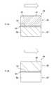
도 1에 도시한 드라이 에칭 장치(10)는, 처리실로서의 진공 챔버(12)와, 상부 전극판(14)과, 기대(16)를 구비한다. 진공 챔버(12)는, 대략 원통 형상이며, 내부에, 원통형의 측벽으로 둘러싸인 처리 공간(31)을 갖는다. 진공 챔버(12)의 측벽의 내면은, 측벽 부재(13)로 덮여 있다. 진공 챔버(12)의 상벽의 상부 전극판(14)의 주위의 내면은, 상벽 부재(17)로 덮여 있다. 측벽 부재(13) 및 상벽 부재(17)는, 진공 챔버(12)의 플라즈마에 노출되는 내벽을 보호하기 위한 환상의 부재이며, 실리콘으로 형성되어 있다.The
진공 챔버(12)는 진공 챔버(12) 내를 높이 방향으로 구획하는 배플판(25)이 설치되어 있다. 배플판(25)으로 구획된 진공 챔버(12) 내의 하측에는 배기 공간(26), 상측에는 처리 공간(31)이 형성되어 있다. 배플판(25)은 에칭 가스의 역류 방지를 위한 보호 부재이며, 실리콘으로 형성되어 있다. 배플판(25)은 환상의 본체를 갖고, 본체에 두께 방향으로 관통된 유통로(27)를 갖는다. 본 도면에 도시한 바와 같이, 배플판(25)은 진공 챔버(12) 내의 높이 방향의 대략 중앙에 설치되어 있다.The
상부 전극판(14)은, 원판 형상의 부재이며, 진공 챔버(12) 내의 상부에 고정되어 있다. 상부 전극판(14)의 주연부는, 보호 링(20)으로 덮여 있다. 상부 전극판(14)과 보호 링(20) 사이에는, 석영으로 형성된 실드링(21)이 설치되어 있다. 보호 링(20)은 상부 전극판(14) 주변에 발생하는 플라즈마로부터 진공 챔버(12)의 내벽을 보호하기 위한 부재이며, 실리콘으로 형성되어 있다. 보호 링(20)은 접지되는 경우도 있다. 본 도면의 경우, 보호 링(20)은 진공 챔버(12) 내측의 표면이, 실드링(21)보다도 돌출되어 있음과 함께, 상벽 부재(17)와 동일한 높이이다. 상부 전극판(14)은 두께 방향으로 관통된 복수의 관통 구멍(15)을 갖는다. 상부 전극판(14)은, 도시하지 않은 고주파 전원이 전기적으로 접속되어 있다. 상부 전극판(14)은 가스 공급관(24)이 접속되어 있다.The
가스 공급관(24)으로부터 공급된 에칭 가스는, 상부 전극판(14)의 관통 구멍(15)으로부터 진공 챔버(12) 내에 유입된다. 진공 챔버(12) 내에 유입된 에칭 가스는, 유통로(27)를 통해 배기 공간(26)으로 유입되고, 배출구(28)로부터 외부로 배출된다.The etching gas supplied from the
기대(16)는, 진공 챔버(12) 내의 배플판(25)의 상측인 처리 공간(31) 내에 설치되어 있고, 그 주위는 그라운드 링(30)으로 둘러싸여 있다. 그라운드 링(30)은 실리콘으로 형성되어 있고, 접지되어 있다. 기대(16) 상에는, 포커스 링(18)이 설치되어 있다. 포커스 링(18)은 실리콘으로 형성되고, 웨이퍼(22)의 주연을 지지하는 오목부(19)가 내측의 전체 둘레에 걸쳐 형성되어 있다. 포커스 링에는, 에칭처리 중의 플라즈마를 안정시키기 위한 전압을 인가하는 전원이 전기적으로 접속되어 있다. 포커스 링(18)의 주위에는, 포커스 링(18)의 측면을 보호하는 커버링(23)을 설치해도 된다. 커버링(23)은 석영으로 형성되고, 포커스 링(18)의 주연을 지지하는 오목부(33)가 내측의 전체 둘레에 걸쳐 형성되어 있다.The
드라이 에칭 장치(10)는, 상부 전극판(14)을 통해 에칭 가스가 공급되고, 고주파 전원으로부터 고주파 전압이 인가되면, 상부 전극판(14)과 웨이퍼(22) 사이에서 플라즈마가 발생한다. 이 플라즈마에 의해 웨이퍼(22) 표면이 에칭된다.In the
본 실시 형태에 관한 링 형상 부재는, 실리콘제 부품으로서의, 상기 포커스 링(18), 보호 링(20), 그라운드 링(30), 측벽 부재(13), 상벽 부재(17), 배플판(25)에 적용 가능하다. 링 형상 부재는, 상기 실리콘제 부품에 한정되지 않는다. 링 형상 부재는, 드라이 에칭 장치(10)의 진공 챔버(12) 내에 설치되며, 전압이 인가되거나, 또는 접지되는 실리콘제 부품이 되는 전극용 링, 및 상기 이외의 실리콘제 부품이 되는 보호재용 링에 적용할 수 있다. 링 형상 부재는, 내경이 290㎜ 이상, 외경은 800㎜ 이하 정도로 할 수 있다.The ring-shaped member according to the present embodiment is the
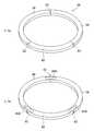
일례로서 포커스 링(18)용의 부재가 되는 본 실시 형태에 관한 링 형상 부재에 대하여 이하 설명한다. 도 2에 도시한 바와 같이, 링 형상 부재(32)는, 복수(본 도면의 경우, 3개)의 제1 실리콘 부재(34, 36, 38)를 구비한다. 또한, 이하의 설명에 있어서, 복수의 제1 실리콘 부재(34, 36, 38)를 특별히 구별하지 않는 경우, 총칭하여 실리콘 부재라 칭한다. 실리콘 부재는, 원호 형상이며, 긴 변 방향의 단부면인 맞댐면(37)에 있어서, 실리콘 접착부(본 도면에는 도시하지 않음)를 개재하여 일방향으로 접합함으로써, 링 형상으로 일체화되어 있다. 실리콘 부재는, 단결정이어도 다결정이어도 되고, 그 제조 방법, 순도, 결정 방위 등에 있어서 한정되지 않는다. 실리콘 부재의 크기는, 특별히 한정되지 않지만, 예를 들어 두께 1㎜ 이상 100㎜ 이하, 폭 10㎜ 이상 100㎜ 이하 정도로 할 수 있다.As an example, a ring-shaped member according to the present embodiment that becomes a member for the
도 3에 도시한 바와 같이, 실리콘 부재끼리의 맞댐면(37)에는, 실리콘 접착부(39A)가 형성되어 있다. 도 3에는, 제1 실리콘 부재(34, 36) 사이의 맞댐면(37)을 도시하고 있다.As shown in Fig. 3, a
실리콘 부재가 단결정인 경우, 실리콘 접착부(39A)는, 맞댐면(37)에서 접하는 실리콘 부재의 단부면의 결정성을 이어받은 단결정 실리콘이 일체화되어 있다. 본 도면의 경우, 실리콘 접착부(39A)는, 실리콘 부재(34)의 단부면의 결정성을 이어받은 단결정 실리콘을 포함하는 하나의 실리콘 접착부와, 실리콘 부재(36)의 단부면 결정성을 이어받은 단결정 실리콘을 포함하는 다른 실리콘 접착부가 일체화되어 있다. 즉 하나의 실리콘 접착부의 결정 방위는, 실리콘 부재(34)의 단부면의 결정 방위와 동일하고, 다른 실리콘 접착부의 결정 방위는, 실리콘 부재(36)의 단부면의 결정 방위와 동일하다.When the silicon member is a single crystal, the
(2) 제조 방법(2) Manufacturing method
다음으로 링 형상 부재(32)를 제조하는 방법에 대하여 설명한다. 먼저 실리콘 부재에 대해 표면 처리를 한다. 구체적으로는, 실리콘 부재의 표면을 연삭 및 연마 등에 의해 가공하고, 바람직하게는 경면으로 한다. 실리콘 부재의 표면을, 불산과 질산의 혼합액 등에 의해 에칭해도 된다. 혼합액으로서는 JIS 규격 H0609에 규정된 화학 연마액(불산(49%) : 질산(70%) : 아세트산(100%)=3 : 5 : 3) 등을 사용할 수 있다.Next, a method of manufacturing the ring-shaped
계속해서, 3개의 제1 실리콘 부재(34, 36, 38)를 링 형상으로 배열한다. 제1 실리콘 부재(34, 36, 38)끼리의 맞댐면(37)의 사이의 실리콘 접착부(39A)는, 맞댐면(37) 근방의 실리콘을 가열하여 융해하여 형성한다. 제1 실리콘 부재(34, 36, 38)를 링 형상으로 배열하였을 때의 맞댐면의 사이의 간극은, 0㎜ 내지 1㎜인 것이 바람직하다. 실리콘은 융해되면 체적이 감소된다. 예를 들어 제1 실리콘 부재(34, 36) 사이의 간극이 1㎜를 초과하면, 제1 실리콘 부재(34)의 단부면의 실리콘 융해물과, 제1 실리콘 부재(36)의 단부면의 실리콘 융해물이 접촉하지 않는다. 그 때문에 제1 실리콘 부재(34)의 단부면의 실리콘 접착부와 제1 실리콘 부재(36)의 단부면의 실리콘 접착부는, 일체화되도록 접합되지 않는다.Subsequently, the three
간극이 1㎜ 이하인 경우, 표면 장력에 의해, 제1 실리콘 부재(34)의 단부면의 실리콘 융해물과, 제1 실리콘 부재(36)의 단부면의 실리콘 융해물이 접촉하고, 모세관 현상에 의해, 간극에 제1 실리콘 부재(34)의 단부면의 실리콘 융해물과, 제1 실리콘 부재(36)의 단부면의 실리콘 융해물이 유입된다. 그 때문에 제1 실리콘 부재(34)의 단부면의 실리콘 접착부와 제1 실리콘 부재(36)의 단부면의 실리콘 접착부는, 원자 레벨로 일체화되어 접합된다.When the gap is less than 1 mm, the silicon melt on the end surface of the
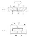
가열 방법은 광 가열에 의해 행할 수 있다. 광 가열은, 가열 부위를 용이하게 이동할 수 있고, 또한 공급하는 전력에 따라서 가열량을 변화시키는 것이 용이하며, 예를 들어 각종 램프, 레이저가 사용된다.The heating method can be performed by light heating. In light heating, the heating portion can be easily moved, and it is easy to change the amount of heating in accordance with the power supplied, and various lamps and lasers are used, for example.
본 실시 형태의 경우, 도 4에 도시한 장치를 사용할 수 있다. 본 도면에 도시한 장치는, 적어도 하나의, 램프(42) 및 당해 램프(42)가 출사하는 광을 집광하는 집광부로서의 타원 미러(44)를 구비한다. 램프(42)로서는, 적외선 결정 성장 장치에 일반적으로 사용되는 크세논 램프나 할로겐 램프를 사용할 수 있다. 출력으로서는 1 내지 30㎾ 정도의 것이 바람직하다. 레이저로서는, 파장 780 내지 1600㎚의 적외선 레이저를 사용할 수 있다. 또한, 취급의 용이성 및 광원의 수명의 관점에서, 반도체 레이저를 복수 모듈화한 파장 780 내지 980㎚, 출력 200 내지 400W 정도의 패키지 타입의 광원을 사용하는 것이 바람직하다.In the case of this embodiment, the device shown in Fig. 4 can be used. The apparatus shown in this figure includes at least one
가열은, 맞댐면(37)의 외측으로부터이면 되고, 실리콘 부재에 대하여 수직 방향으로는 한정되지 않고, 경사로부터여도 된다.Heating may be performed from the outside of the abutting
집광 영역은, 통상 직경 10 내지 30㎜ 정도이다. 집광 영역은, 램프(42)의 발광 위치를 타원 미러(44)의 초점으로부터 어긋나게 함으로써, 30 내지 100㎜ 정도로 확대된다. 집광 영역이 확대됨으로써, 가열 범위를 넓힐 수 있다. 집광 영역을, 맞댐면(37)의 링 형상 부재(32)에 있어서의 상면의 전역에 걸쳐 주사시켜 가열하는 것이 바람직하다.The condensing area is usually about 10 to 30 mm in diameter. The condensing area is enlarged to about 30 to 100 mm by shifting the light emission position of the
먼저, 타원 미러(44)의 초점 위치와 램프(42)의 발광부의 위치를 합치시키도록 램프 위치를 조정하고, 실리콘 부재의 상면 높이를 타원 미러(44)의 또 하나의 초점 위치가 되도록 조정함으로써, 조사 위치에서의 타원 미러(44)의 확대를 약 3㎜로 한다. 이 상태에서, 타원 미러(44)를 맞댐면(37)의 위치에 맞추고 램프(42)의 파워를 올린다. 가열을 개시하면, 맞댐면(37)의 상면측이 융해되어 실리콘 융해물이 생성된다. 구체적으로는, 램프 정격의 60%에서 상면이 녹기 시작하고(표면 온도가 1420℃로 추정됨), 램프 정격의 90%에서 맞댐면(37)의 사이에, 맞댐면(37)에서 접하는 실리콘이 융해되고 실리콘 융해물이 모세관 현상에 의해 유입되어 맞댐면(37)의 사이의 일부를 막는다. 이 상태에서, 타원 미러(44)를 맞댐면(37)을 따라서 일정한 속도, 예를 들어 5㎜/분의 속도로 주사함으로써, 맞댐면(37)의 사이를 융해 실리콘으로 매립하여, 막을 수 있다. 타원 미러(44)를 맞댐면(37)의 외연 중, 링 형상 부재(32)에 있어서의 상면측에 걸쳐 주사시켜 가열한다. 덧붙여서 링 형상 부재의 하면측에 있어서 맞댐면(37)을 마찬가지의 방법에 의해 가열해도 된다.First, by adjusting the lamp position to match the focal position of the
계속해서, 융해된 맞댐면(37)의 상면을 냉각하여, 실리콘 융해물을 실리콘 부재의 결정에 따라서 결정화시킨다. 구체적으로는 실리콘 융해물이 굳어지기 시작하는 램프 정격의 60%까지 2분에 걸쳐 램프(42)의 파워를 낮추고, 그 상태에서 5분 유지한다. 이때의 표면 온도는 1400℃ 내지 1415℃이다. 실리콘 융해물은, 맞댐면(37)에서 접하는 실리콘 부재의 단부면의 결정성을 이어받은 실리콘 접착부(39A)가 된다. 실리콘 접착부(39A)는, 실리콘 부재가 단결정인 경우, 한쪽의 실리콘 부재의 단부면의 결정성을 이어받은 단결정 실리콘을 포함하는 하나의 실리콘 접착부와, 다른 쪽의 실리콘 부재의 단부면의 결정성을 이어받은 단결정 실리콘을 포함하는 다른 실리콘 접착부가 일체화된다.Subsequently, the upper surface of the melted abutting
상기의 수순에 의해, 모든 맞댐면(37)에 있어서, 실리콘 접착부(39A)를 마찬가지로 형성함으로써, 제1 실리콘 부재(34, 36, 38)끼리를 접합하여, 링 형상 부재(32)를 형성할 수 있다.According to the above procedure, by forming the
상기와 같이 하여 얻어진 링 형상 부재(32)는, 기계 가공에 의해 내측의 전체 둘레에 걸쳐 오목부를 형성함으로써, 포커스 링(18)이 될 수 있다.The ring-shaped
링 형상 부재(32)는, 실리콘제 부품의 외경보다 작은 웨이퍼용 실리콘 결정 잉곳으로부터 잘라낸 3개 이상의 실리콘 부재를 조합하여 제조할 수 있다. 따라서 링 형상 부재(32)는, 실리콘제 부품의 외경보다 큰 웨이퍼용 실리콘 결정 잉곳을 사용할 필요가 없으므로, 그만큼 비용을 저감할 수 있다.The ring-shaped
본 실시 형태에 관한 링 형상 부재(32)는, 맞댐면(37)이 실리콘 접착부(39A)에 의해 접합되어 있으므로, 진공 챔버(12) 내에 있어서 플라즈마가 조사되어도, 진공 챔버(12) 내가 오염되는 일이 없다.In the ring-shaped
(3) 변형예(3) Modification example
본 실시 형태의 경우, 맞댐면(37)에서 접하는 단부면의 실리콘을 융해하여, 실리콘 접착부(39A)를 형성하는 경우에 대하여 설명하였지만, 본 발명은 이것에 한정되지 않는다. 도 5에 도시한 바와 같이, 맞댐면 상에 단결정 또는 다결정의 실리콘편(40)을 두고, 당해 실리콘편(40)을 융해하여 실리콘 접착부(39B)를 형성해도 된다. 실리콘편(40)을 사용하지 않는 경우, 맞댐면(37)의 상면측의 실리콘이 융해되어, 맞댐면(37)의 사이에 유입됨으로써, 맞댐면(37)의 상면이 오목해지는 경우가 있다. 실리콘편(40)을 사용하여 실리콘 접착부(39B)를 형성함으로써, 실리콘 접착부(39B)가 형성된 후의 맞댐면(37)의 상면(55)이 오목해지는 것을 방지할 수 있다(도 6). 실리콘편(40)은 맞댐면(37)의 사이의 체적과, 동일한 체적인 것이 바람직하다.In the case of the present embodiment, a case has been described in which the silicon of the end surface in contact with the abutting
2. 제2 실시 형태2. Second embodiment
다음으로 제2 실시 형태에 관한 링 형상 부재에 대하여 설명한다. 또한, 상기 제1 실시 형태와 마찬가지의 구성에 대해서는 마찬가지의 부호를 붙이고, 설명을 생략한다. 도 7에 도시한 링 형상 부재(46)는, 제1 링체(35)와, 제2 링체(47)를 구비한다. 본 도면에 도시한 제1 링체(35)는, 제1 실리콘 부재(41, 43, 45)를 구비하고, 상기 제1 실시 형태의 링 형상 부재(32)에 비해 폭이 작은 점만이 상이하다. 제2 링체(47)는, 복수(본 도면의 경우 3개)의 제2 실리콘 부재(48, 50, 52)를 구비한다. 제2 실리콘 부재(48, 50, 52)는, 설명의 편의상, 부호를 바꾸었지만, 제1 실리콘 부재(41, 43, 45)와 동일하다. 제1 링체(35)와 제2 링체(47)는, 실리콘 부재끼리의 맞댐면(49)이 원주 방향으로 어긋난 상태에서 접합면(54)에 있어서 동축상에 겹쳐 있다.Next, a ring-shaped member according to the second embodiment will be described. In addition, the same reference numerals are attached to the same configurations as those in the first embodiment, and the description is omitted. The ring-shaped
도 8a에는 제1 실리콘 부재(41, 43) 사이의 맞댐면(49), 도 8b에는 제2 실리콘 부재(48, 52) 사이의 맞댐면(49)을 도시하고 있다. 도면 중 화살표의 방향은, 링 형상 부재(46)의 반경 방향의 외측 방향을 나타낸다.Fig. 8A shows a
제1 실리콘 부재(41, 43) 사이의 맞댐면(49)에는, 제1 실리콘 접착부(51)가 형성되어 있다(도 8a). 제1 링체(35)와 제2 링체(47) 사이의 접합면(54)에는, 제2 실리콘 접착부(53)가 형성되어 있다. 제2 실리콘 부재(48, 52) 사이의 맞댐면(49)에는, 제1 실리콘 접착부가 형성되어 있지 않다(도 8b).A first
이와 같이 하여 제1 실리콘 접착부(51)는, 제1 실리콘 부재(41, 43, 45)끼리의 맞댐면(49)의 사이, 및 제1 링체(35)와 제2 링체(47)의 접합면(54)의 사이를 막고 있다.In this way, the first
다음으로, 본 실시 형태의 링 형상 부재(46)의 제조 방법에 대하여 설명한다. 또한, 상기 제1 실시 형태와 마찬가지의 공정에 대해서는 적절히 설명을 생략한다. 먼저 표면 처리 후의 3개의 제2 실리콘 부재(48, 50, 52)를 링 형상으로 배열한다. 다음에, 제2 실리콘 부재(48, 50, 52)의 상면에 3개의 제1 실리콘 부재(41, 43, 45)를 둔다. 제1 실리콘 부재(41, 43, 45)는, 먼저 배치된 제2 실리콘 부재(48, 50, 52)에 대해, 긴 변 방향의 길이의 절반만큼 어긋나게 하여 배치한다. 상기와 같이 하여, 제2 실리콘 부재(48, 50, 52) 상에, 제1 실리콘 부재(41, 43, 45)가 적재된 상태가 된다.Next, the manufacturing method of the ring-shaped
다음으로, 제1 실리콘 부재(34, 36, 38)측으로부터 가열하여, 제1 실리콘 부재(41, 43, 45)끼리의 맞댐면(49)의 사이에 실리콘의 융해물을 생성하여, 제1 실리콘 접착부(51)를 형성한다. 가열 조건, 냉각 조건은, 상기 제1 실시 형태와 마찬가지로 할 수 있다.Next, by heating from the side of the
계속해서, 제1 링체(35) 및 제2 링체(47) 사이의 접합면(54)의 사이의 실리콘을 가열하여 융해한다. 융해된 실리콘은, 모세관 현상에 의해 수평 방향인 접합면(54)의 사이에 유입되어, 제2 실리콘 접착부(53)를 형성한다.Subsequently, silicon between the bonding surfaces 54 between the
본 실시 형태의 링 형상 부재(46)는, 맞댐면(49)의 사이에 제1 실리콘 접착부(51), 및, 접합면(54)의 사이가 제2 실리콘 접착부(53)로 접합되어 있으므로, 상기 제1 실시 형태와 마찬가지의 효과를 얻을 수 있다.In the ring-shaped
본 실시 형태의 경우, 맞댐면(49)에서 접하는 단부면의 실리콘을 융해하여, 제1 실리콘 접착부(51)를 형성하는 경우에 대하여 설명하였지만, 본 발명은 이것에 한정되지 않는다. 상기 도 5에 도시한 바와 같이, 맞댐면 상에 실리콘편(40)을 두고, 당해 실리콘편(40)을 융해하여 제1 실리콘 접착부를 형성해도 된다.In the case of the present embodiment, a case has been described in which the silicon of the end surface in contact with the abutting
본 실시 형태의 경우, 상기 제1 실시 형태의 링 형상 부재(32)에 비해 폭이 작은 경우에 대하여 설명하였지만, 본 발명은 이것에 한정되지 않는다. 제1 링체와 제2 링체 사이의 접합면을 충분한 기계적 강도를 갖도록 접합할 수 있으면, 링 형상 부재의 폭은 적절히 선택할 수 있다.In the case of this embodiment, the case where the width is smaller than that of the ring-shaped
제2 실리콘 부재(48, 52) 사이의 맞댐면(49)에는, 제1 실리콘 접착부를 형성하지 않은 경우에 대하여 설명하였지만, 본 발명은 이것에 한정되지 않는다. 제2 실리콘 부재(48, 52) 사이의 맞댐면(49)에 제1 실리콘 접착부를 형성해도 된다.Although the case where the first silicone adhesive portion is not formed on the abutting
3. 제3 실시 형태3. Third embodiment
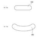
다음으로 제3 실시 형태에 관한 링 형상 부재에 대하여 설명한다. 도 9a, 도 9b에 도시한 링 형상 부재(56)는, 복수(본 도면의 경우, 3개)의 제1 실리콘 부재(58, 60, 62)와, 제1 실리콘 부재(58, 60, 62)끼리에 걸치는 위치에 매립된 복수(3개)의 매립 실리콘 부재(64A)를 구비한다. 매립 실리콘 부재(64A)는, 링 형상 부재(56)의 플라즈마가 조사되는 측과 반대측, 본 도면의 경우, 하면측에 형성된다.Next, a ring-shaped member according to the third embodiment will be described. The ring-shaped
매립 실리콘 부재(64A)는, 실리콘 부재와 동일한 재료로 형성되는 것이 바람직하다. 매립 실리콘 부재(64A)의 4코너는, R 가공되어 있는 것이 바람직하다. 매립 실리콘 부재(64A)는, 4코너가 R 가공되어 있음으로써, 결함 등의 손상을 방지할 수 있다. R은 3㎜ 이상인 것이 바람직하다.It is preferable that the embedded
매립 실리콘 부재(64A)는, 하면이, 실리콘 부재의 하면과 대략 동일한 높이가 되도록 형성되는 것이 바람직하다. 매립 실리콘 부재(64A)의 두께는, 실리콘 부재의 두께의 20 내지 80%가 바람직하고, 40 내지 60%가 보다 바람직하다.It is preferable that the embedded
매립 실리콘 부재(64A)는, 직사각형의 판 형상 부재를 포함하고, 평면에서 보아 링 형상 부재(56)로부터 돌출되지 않는 크기인 것이 바람직하다. 매립 실리콘 부재(64A)의 긴 변 방향의 길이는, 링 형상 부재(56)의 외주 길이의 2 내지 10%인 것이 바람직하다.It is preferable that the embedded
보다 구체적인 실리콘 부재의 사이즈는, 내주 직경 340㎜, 외주 직경 420㎜, 두께 4㎜의 링을, 3분할한 크기로 할 수 있다. 매립 실리콘 부재(64A)는, 길이 60㎜, 폭 25㎜, 4코너에 5㎜의 R 가공을 실시한 두께 2㎜로 할 수 있다. 실리콘 부재의 하면에 형성되는 구멍은, 실리콘의 소편의 형상에 대응한 형상으로 하고, 깊이는 2㎜로 한다. 이 경우, 매립 실리콘 부재(64A)의 두께는 실리콘 부재의 두께의 50%, 매립 실리콘 부재(64A)의 긴 변 방향의 길이는 링 형상 부재(56)의 외주 길이의 5%이다.A more specific size of the silicone member may be a ring having an inner circumferential diameter of 340 mm, an outer circumferential diameter of 420 mm, and a thickness of 4 mm divided into three. The embedded
도 10a, 도 10b에 도시한 바와 같이, 실리콘 부재의 하면에는, 긴 변 방향의 단부에, 저면을 갖는 구멍이 형성되어 있다. 도 10a, 도 10b에는, 제1 실리콘 부재(58, 60) 사이의 맞댐면(63A)을 도시하고 있다. 매립 실리콘 부재(64A)는, 당해 구멍에 매립된다. 제1 실리콘 부재(58, 60, 62)끼리의 맞댐면(63A)의 사이에는, 제1 실리콘 접착부(68)가 형성되어 있다. 매립 실리콘 부재(64A)의 주연과, 제1 실리콘 부재(58, 60, 62)의 구멍 내면 사이에는, 제2 실리콘 접착부(70)가 형성되어 있다.As shown in Figs. 10A and 10B, a hole having a bottom surface is formed on the lower surface of the silicon member at an end portion in the long side direction. 10A and 10B, the abutting
본 실시 형태에 관한 맞댐면에 있어서의 제1 실리콘 접착부(68)는, 상기 제1 실시 형태와 마찬가지의 방법에 의해, 형성할 수 있다. 제2 실리콘 접착부(70)는, 실리콘 부재의 하면측으로부터 매립 실리콘 부재(64A)의 주연과 제1 실리콘 부재(58, 60, 62)의 구멍 내면의 근방의 실리콘을, 상기 제1 실시 형태와 마찬가지의 방법에 의해 가열하여, 실리콘의 융해물을 생성함으로써, 형성할 수 있다.The first
본 실시 형태의 링 형상 부재(56)는, 매립 실리콘 부재(64A)를 형성함으로써, 실리콘 부재끼리의 사이의 접합 면적을 크게 할 수 있으므로, 기계적 강도를 보다 크게 할 수 있다. 또한, 링 형상 부재(56)는, 맞댐면(63A)의 사이가 제1 실리콘 접착부(68)로 접합되어 있음으로써, 상기 제1 실시 형태와 마찬가지의 효과를 얻을 수 있다.In the ring-shaped
매립 실리콘 부재(64A)는, 직사각형일 필요는 없고, 예를 들어 도 11a, 도 11b에 도시한 바와 같이, 타원 형상의 매립 실리콘 부재(64B)(도 11a), 원호 형상의 매립 실리콘 부재(64C)(도 11b)여도 된다. 또한 매립 실리콘 부재(64B, 64C)의 긴 변 방향 단부는, 도 11a, 도 11b에 도시한 바와 같이, 반원 형상이어도 된다.The embedded
본 실시 형태의 경우, 맞댐면(63A)에서 접하는 단부면의 실리콘을 융해하여, 제1 실리콘 접착부(68)를 형성하는 경우에 대하여 설명하였지만, 본 발명은 이것에 한정되지 않는다. 도 5에 도시한 바와 같이, 맞댐면 상에 실리콘편(40)을 두고, 당해 실리콘편(40)을 융해하여 제1 실리콘 접착부를 형성해도 된다.In the case of the present embodiment, a case has been described in which the silicon of the end surface in contact with the
12 : 진공 챔버(처리실)
22 : 웨이퍼(기판)
32 : 링 형상 부재
34, 36, 38 : 제1 실리콘 부재(실리콘 부재)
37 : 맞댐면
39A, 39B : 실리콘 접착부
41, 43, 45 : 제1 실리콘 부재(실리콘 부재)
48, 50, 52 : 제2 실리콘 부재(실리콘 부재)
49 : 맞댐면
51 : 제1 실리콘 접착부(실리콘 접착부)
53 : 제2 실리콘 접착부(실리콘 접착부)
58, 60, 62 : 제1 실리콘 부재(실리콘 부재)
63A : 맞댐면
64A, 64B, 64C : 매립 실리콘 부재
68 : 제1 실리콘 접착부(실리콘 접착부)
70 : 제2 실리콘 접착부(실리콘 접착부)12: vacuum chamber (treatment chamber)
22: wafer (substrate)
32: ring-shaped member
34, 36, 38: first silicon member (silicon member)
37: abutting surface
39A, 39B: silicone adhesive
41, 43, 45: first silicon member (silicon member)
48, 50, 52: second silicon member (silicon member)
49: abutting surface
51: first silicone adhesive portion (silicon adhesive portion)
53: second silicone adhesive portion (silicon adhesive portion)
58, 60, 62: first silicon member (silicon member)
63A: butt face
64A, 64B, 64C: embedded silicon member
68: first silicone adhesive portion (silicon adhesive portion)
70: second silicone adhesive portion (silicon adhesive portion)
Claims (6)
Translated fromKorean단결정 실리콘 또는 다결정 실리콘을 포함하는 하나의 실리콘 부재의 하나의 맞댐면과, 단결정 실리콘 또는 다결정 실리콘을 포함하는 다른 실리콘 부재의 다른 맞댐면이, 맞대지도록 배치하는 공정과,
상기 하나의 맞댐면과 상기 다른 맞댐면을 크세논 램프 또는 할로겐 램프에 의해 행해지는 광 가열에 의해 가열하여, 상기 하나의 맞댐면의 표면의 실리콘과 상기 다른 맞댐면의 표면의 실리콘을 융해하고, 상기 하나의 맞댐면과 상기 다른 맞댐면 사이에 실리콘 융해물이 유입되도록 하는 공정과,
상기 하나의 맞댐면과 상기 다른 맞댐면을 냉각하여, 상기 실리콘 융해물을 결정화시켜 실리콘 접착부를 형성하고, 상기 하나의 실리콘 부재와 상기 다른 실리콘 부재를 상기 실리콘 접착부를 개재하여 접합하는 공정을 포함하는 것을 특징으로 하는 링 형상 부재의 제조 방법.A method for manufacturing a ring-shaped member installed in a processing chamber in which the substrate is accommodated in a substrate processing apparatus for performing plasma treatment on a substrate,
A step of arranging so that one abutting surface of one silicon member including single crystal silicon or polycrystalline silicon and the other abutting surface of another silicon member including single crystal silicon or polycrystalline silicon are abutted,
The one abutting surface and the other abutting surface are heated by light heating performed by a xenon lamp or a halogen lamp to melt the silicon of the surface of the one abutting surface and the silicon of the surface of the other abutting surface, and the A process of allowing a silicon melt to flow between one abutting surface and the other abutting surface,
Cooling the one abutting surface and the other abutting surface to crystallize the silicon melt to form a silicon bonding unit, and bonding the one silicon member and the other silicon member through the silicon bonding unit. A method of manufacturing a ring-shaped member, characterized in that.
단결정 실리콘 또는 다결정 실리콘을 포함하는 하나의 실리콘 부재의 하나의 맞댐면과, 단결정 실리콘 또는 다결정 실리콘을 포함하는 다른 실리콘 부재의 다른 맞댐면이, 간극을 두고 맞대지도록 배치하는 공정과,
상기 하나의 맞댐면과 상기 다른 맞댐면을 광 가열에 의해 가열하여, 상기 하나의 맞댐면의 표면의 실리콘과 상기 다른 맞댐면의 표면의 실리콘을 융해하여 접촉시키고, 상기 하나의 맞댐면과 상기 다른 맞댐면 사이의 상기 간극에 실리콘 융해물이 모세관 현상에 의해 유입되도록 하는 공정과,
상기 하나의 맞댐면과 상기 다른 맞댐면을 냉각하여, 상기 실리콘 융해물을 결정화시켜 실리콘 접착부를 형성하고, 상기 하나의 실리콘 부재와 상기 다른 실리콘 부재를 상기 실리콘 접착부를 개재하여 접합하는 공정을 포함하는 것을 특징으로 하는 링 형상 부재의 제조 방법.A method for manufacturing a ring-shaped member installed in a processing chamber in which the substrate is accommodated in a substrate processing apparatus for performing plasma treatment on a substrate,
A step of arranging so that one abutting surface of one silicon member including single crystal silicon or polycrystalline silicon and another abutting surface of another silicon member including single crystal silicon or polycrystalline silicon are abutted with a gap,
The one abutting surface and the other abutting surface are heated by light heating to melt and contact the silicon of the surface of the one abutting surface and the silicon of the surface of the other abutting surface, and the one abutting surface and the other A process of allowing a silicon melt to flow into the gap between the mating surfaces by a capillary phenomenon,
Cooling the one abutting surface and the other abutting surface to crystallize the silicon melt to form a silicon bonding unit, and bonding the one silicon member and the other silicon member through the silicon bonding unit. A method of manufacturing a ring-shaped member, characterized in that.
상기 광 가열이, 크세논 램프 또는 할로겐 램프에 의해 행해지는 것을 특징으로 하는 링 형상 부재의 제조 방법.The method of claim 2,
The method for manufacturing a ring-shaped member, wherein the light heating is performed by a xenon lamp or a halogen lamp.
단결정 실리콘 또는 다결정 실리콘을 포함하는 복수의 실리콘 부재와,
하나의 상기 실리콘 부재의 하나의 맞댐면과 다른 상기 실리콘 부재의 다른 맞댐면 사이의 간극을 매립하도록 형성되며, 상기 하나의 맞댐면과 상기 다른 맞댐면을 접합하는 실리콘 접착부를 구비하고,
상기 실리콘 접착부는, 상기 하나의 상기 실리콘 부재의 단부면의 실리콘 융해물과 상기 다른 상기 실리콘 부재의 단부면의 실리콘 융해물이 접촉하고 모세관 현상에 의해 상기 간극에 유입되어 결정화된 것이며, 상기 하나의 맞댐면의 결정성을 이어받은 단결정 실리콘을 포함하는 하나의 실리콘 접착부와 상기 다른 맞댐면의 결정성을 이어받은 단결정 실리콘을 포함하는 다른 실리콘 접착부가 원자 레벨로 일체화되어 있는 것을 특징으로 하는 링 형상 부재.A ring-shaped member installed in a processing chamber in which the substrate is accommodated in a substrate processing apparatus for performing plasma treatment on a substrate,
A plurality of silicon members including single crystal silicon or polycrystalline silicon,
It is formed to fill a gap between one abutting surface of the one silicon member and the other abutting surface of the other silicon member, and has a silicone adhesive portion for bonding the one abutting surface and the other abutting surface,
The silicon adhesive portion is crystallized by contacting the silicon melt of the end surface of the one silicon member with the silicon melt of the end surface of the other silicon member and flowing into the gap by a capillary phenomenon, and the one Ring-shaped member, characterized in that one silicon bonding portion including single crystal silicon inherited from the crystallinity of the abutting surface and another silicon bonding portion including single crystal silicon inherited from the crystallinity of the other facing surface are integrated at an atomic level .
상기 간극이 1㎜ 이하인 것을 특징으로 하는 링 형상 부재.The method of claim 4,
The ring-shaped member, wherein the gap is 1 mm or less.
상기 링 형상 부재는 두께가 4㎜ 이상 100㎜ 이하인 것을 특징으로 하는 링 형상 부재.The method according to claim 4 or 5,
The ring-shaped member has a thickness of 4 mm or more and 100 mm or less.
Applications Claiming Priority (3)
| Application Number | Priority Date | Filing Date | Title |
|---|---|---|---|
| JP2017100173AJP6278498B1 (en) | 2017-05-19 | 2017-05-19 | Ring-shaped member manufacturing method and ring-shaped member |
| JPJP-P-2017-100173 | 2017-05-19 | ||
| PCT/JP2018/008870WO2018211788A1 (en) | 2017-05-19 | 2018-03-07 | Method for manufacturing annular member and annular member |
Publications (2)
| Publication Number | Publication Date |
|---|---|
| KR20190002635A KR20190002635A (en) | 2019-01-08 |
| KR102214968B1true KR102214968B1 (en) | 2021-02-09 |
Family
ID=61195744
Family Applications (1)
| Application Number | Title | Priority Date | Filing Date |
|---|---|---|---|
| KR1020187034663AActiveKR102214968B1 (en) | 2017-05-19 | 2018-03-07 | Ring-shaped member manufacturing method and ring-shaped member |
Country Status (8)
| Country | Link |
|---|---|
| US (2) | US10984988B2 (en) |
| EP (1) | EP3454361B1 (en) |
| JP (1) | JP6278498B1 (en) |
| KR (1) | KR102214968B1 (en) |
| CN (1) | CN109287126B (en) |
| SG (1) | SG11201810732UA (en) |
| TW (1) | TWI765004B (en) |
| WO (1) | WO2018211788A1 (en) |
Families Citing this family (2)
| Publication number | Priority date | Publication date | Assignee | Title |
|---|---|---|---|---|
| CN114388324B (en)* | 2020-10-22 | 2025-05-09 | 中微半导体设备(上海)股份有限公司 | A grounding ring and plasma etching equipment |
| JP7725098B1 (en)* | 2024-03-04 | 2025-08-19 | 日本新工芯技株式会社 | Silicon bonded body manufacturing apparatus and silicon bonded body manufacturing method |
Citations (2)
| Publication number | Priority date | Publication date | Assignee | Title |
|---|---|---|---|---|
| JP2008251744A (en)* | 2007-03-29 | 2008-10-16 | Tokyo Electron Ltd | Plasma processing equipment |
| JP2010114313A (en)* | 2008-11-07 | 2010-05-20 | Tokyo Electron Ltd | Ring-shaped member and method for manufacturing same |
Family Cites Families (19)
| Publication number | Priority date | Publication date | Assignee | Title |
|---|---|---|---|---|
| EP0615431A4 (en)* | 1992-08-27 | 1995-04-19 | Craig John Hubbard | An ankle brace. |
| JP2907375B2 (en)* | 1994-04-21 | 1999-06-21 | 古河電気工業株式会社 | Dust proof ring for conduit air cable connection |
| JP2003257807A (en)* | 2002-03-07 | 2003-09-12 | Shin Etsu Chem Co Ltd | Method of manufacturing silicon processed product and silicon processed product |
| US7083694B2 (en)* | 2003-04-23 | 2006-08-01 | Integrated Materials, Inc. | Adhesive of a silicon and silica composite particularly useful for joining silicon parts |
| US7074693B2 (en)* | 2003-06-24 | 2006-07-11 | Integrated Materials, Inc. | Plasma spraying for joining silicon parts |
| TW200520632A (en)* | 2003-09-05 | 2005-06-16 | Tokyo Electron Ltd | Focus ring and plasma processing apparatus |
| JP5110772B2 (en)* | 2004-02-03 | 2012-12-26 | 株式会社半導体エネルギー研究所 | Manufacturing method of substrate having semiconductor thin film layer |
| KR100684544B1 (en)* | 2005-07-15 | 2007-02-20 | 호서대학교 산학협력단 | Stress measuring device of wafer in high temperature processing |
| JP5424445B2 (en)* | 2007-06-12 | 2014-02-26 | 国立大学法人京都工芸繊維大学 | Semiconductor substrate manufacturing method and semiconductor substrate |
| US8679288B2 (en)* | 2008-06-09 | 2014-03-25 | Lam Research Corporation | Showerhead electrode assemblies for plasma processing apparatuses |
| KR101017160B1 (en)* | 2008-06-17 | 2011-02-25 | 주식회사 동부하이텍 | How to form fluorine diffusion barrier |
| KR101041947B1 (en)* | 2008-12-23 | 2011-06-15 | 청주대학교 산학협력단 | SIO thin film heat treatment apparatus |
| WO2010150590A1 (en)* | 2009-06-24 | 2010-12-29 | キヤノンアネルバ株式会社 | Vacuum heating/cooling apparatus and method of producing magnetoresistive element |
| JP5952550B2 (en)* | 2011-11-28 | 2016-07-13 | 株式会社半導体エネルギー研究所 | Bonding device |
| JP5955658B2 (en)* | 2012-06-15 | 2016-07-20 | 株式会社Screenホールディングス | Heat treatment method and heat treatment apparatus |
| WO2014034180A1 (en)* | 2012-08-28 | 2014-03-06 | 株式会社リケン | Piston ring |
| TWM464809U (en)* | 2012-10-20 | 2013-11-01 | Applied Materials Inc | Focus ring segment and assembly |
| TW201432826A (en)* | 2013-02-01 | 2014-08-16 | Chipbond Technology Corp | Semiconductor packaging process and structure thereof |
| JP5615454B1 (en)* | 2014-02-25 | 2014-10-29 | コバレントマテリアル株式会社 | Focus ring |
- 2017
- 2017-05-19JPJP2017100173Apatent/JP6278498B1/enactiveActive
- 2018
- 2018-03-07CNCN201880002209.8Apatent/CN109287126B/enactiveActive
- 2018-03-07WOPCT/JP2018/008870patent/WO2018211788A1/ennot_activeCeased
- 2018-03-07EPEP18802750.2Apatent/EP3454361B1/enactiveActive
- 2018-03-07KRKR1020187034663Apatent/KR102214968B1/enactiveActive
- 2018-03-07USUS16/307,849patent/US10984988B2/enactiveActive
- 2018-03-07SGSG11201810732UApatent/SG11201810732UA/enunknown
- 2018-03-14TWTW107108692Apatent/TWI765004B/enactive
- 2021
- 2021-03-21USUS17/207,693patent/US11551915B2/enactiveActive
Patent Citations (2)
| Publication number | Priority date | Publication date | Assignee | Title |
|---|---|---|---|---|
| JP2008251744A (en)* | 2007-03-29 | 2008-10-16 | Tokyo Electron Ltd | Plasma processing equipment |
| JP2010114313A (en)* | 2008-11-07 | 2010-05-20 | Tokyo Electron Ltd | Ring-shaped member and method for manufacturing same |
Also Published As
| Publication number | Publication date |
|---|---|
| CN109287126B (en) | 2021-11-09 |
| TW201902307A (en) | 2019-01-01 |
| CN109287126A (en) | 2019-01-29 |
| KR20190002635A (en) | 2019-01-08 |
| EP3454361B1 (en) | 2021-05-26 |
| SG11201810732UA (en) | 2018-12-28 |
| EP3454361A1 (en) | 2019-03-13 |
| TWI765004B (en) | 2022-05-21 |
| US11551915B2 (en) | 2023-01-10 |
| WO2018211788A1 (en) | 2018-11-22 |
| US20210225617A1 (en) | 2021-07-22 |
| JP2018195764A (en) | 2018-12-06 |
| US10984988B2 (en) | 2021-04-20 |
| US20190259581A1 (en) | 2019-08-22 |
| JP6278498B1 (en) | 2018-02-14 |
| EP3454361A4 (en) | 2020-03-11 |
Similar Documents
| Publication | Publication Date | Title |
|---|---|---|
| KR102214968B1 (en) | Ring-shaped member manufacturing method and ring-shaped member | |
| US10553405B2 (en) | Ring-shaped electrode | |
| KR102575442B1 (en) | Ring for Electrode | |
| KR102586861B1 (en) | Ring for protective material | |
| US11380525B2 (en) | Ring for electrode | |
| US10580621B2 (en) | Electrode Plate |
Legal Events
| Date | Code | Title | Description |
|---|---|---|---|
| A201 | Request for examination | ||
| PA0105 | International application | Patent event date:20181129 Patent event code:PA01051R01D Comment text:International Patent Application | |
| PA0201 | Request for examination | ||
| PG1501 | Laying open of application | ||
| E902 | Notification of reason for refusal | ||
| PE0902 | Notice of grounds for rejection | Comment text:Notification of reason for refusal Patent event date:20200226 Patent event code:PE09021S01D | |
| E601 | Decision to refuse application | ||
| PE0601 | Decision on rejection of patent | Patent event date:20200805 Comment text:Decision to Refuse Application Patent event code:PE06012S01D Patent event date:20200226 Comment text:Notification of reason for refusal Patent event code:PE06011S01I | |
| X091 | Application refused [patent] | ||
| AMND | Amendment | ||
| PX0901 | Re-examination | Patent event code:PX09011S01I Patent event date:20200805 Comment text:Decision to Refuse Application | |
| E902 | Notification of reason for refusal | ||
| PE0902 | Notice of grounds for rejection | Comment text:Notification of reason for refusal Patent event date:20201023 Patent event code:PE09021S01D | |
| PX0701 | Decision of registration after re-examination | Patent event date:20210115 Comment text:Decision to Grant Registration Patent event code:PX07013S01D Patent event date:20201005 Comment text:Amendment to Specification, etc. Patent event code:PX07012R01I Patent event date:20200805 Comment text:Decision to Refuse Application Patent event code:PX07011S01I | |
| X701 | Decision to grant (after re-examination) | ||
| GRNT | Written decision to grant | ||
| PR0701 | Registration of establishment | Comment text:Registration of Establishment Patent event date:20210204 Patent event code:PR07011E01D | |
| PR1002 | Payment of registration fee | Payment date:20210204 End annual number:3 Start annual number:1 | |
| PG1601 | Publication of registration | ||
| PR1001 | Payment of annual fee | Payment date:20250203 Start annual number:5 End annual number:5 |