KR102213223B1 - Organic light-emitting display apparatus and manufacturing the same - Google Patents
Organic light-emitting display apparatus and manufacturing the sameDownload PDFInfo
- Publication number
- KR102213223B1 KR102213223B1KR1020140062609AKR20140062609AKR102213223B1KR 102213223 B1KR102213223 B1KR 102213223B1KR 1020140062609 AKR1020140062609 AKR 1020140062609AKR 20140062609 AKR20140062609 AKR 20140062609AKR 102213223 B1KR102213223 B1KR 102213223B1
- Authority
- KR
- South Korea
- Prior art keywords
- lower substrate
- insulating layer
- disposed
- sealing member
- thin film
- Prior art date
- Legal status (The legal status is an assumption and is not a legal conclusion. Google has not performed a legal analysis and makes no representation as to the accuracy of the status listed.)
- Active
Links
- 238000004519manufacturing processMethods0.000titleclaimsabstractdescription17
- 239000000758substrateSubstances0.000claimsabstractdescription182
- 238000007789sealingMethods0.000claimsabstractdescription126
- 239000010409thin filmSubstances0.000claimsabstractdescription84
- 230000002093peripheral effectEffects0.000claimsabstractdescription63
- 230000004888barrier functionEffects0.000claimsabstractdescription54
- 238000000034methodMethods0.000claimsabstractdescription33
- 239000011810insulating materialSubstances0.000claimsdescription9
- 230000001678irradiating effectEffects0.000claimsdescription5
- 239000010410layerSubstances0.000abstractdescription228
- 239000003795chemical substances by applicationSubstances0.000abstract1
- 239000012044organic layerSubstances0.000abstract1
- 101100489584Solanum lycopersicum TFT1 geneProteins0.000description33
- 239000000463materialSubstances0.000description21
- 239000010408filmSubstances0.000description14
- 239000004065semiconductorSubstances0.000description12
- 230000008569processEffects0.000description11
- PXHVJJICTQNCMI-UHFFFAOYSA-NNickelChemical compound[Ni]PXHVJJICTQNCMI-UHFFFAOYSA-N0.000description10
- KDLHZDBZIXYQEI-UHFFFAOYSA-NPalladiumChemical compound[Pd]KDLHZDBZIXYQEI-UHFFFAOYSA-N0.000description10
- 239000011575calciumSubstances0.000description10
- BASFCYQUMIYNBI-UHFFFAOYSA-NplatinumChemical compound[Pt]BASFCYQUMIYNBI-UHFFFAOYSA-N0.000description10
- 239000011777magnesiumSubstances0.000description9
- 229910052581Si3N4Inorganic materials0.000description8
- VYPSYNLAJGMNEJ-UHFFFAOYSA-NSilicium dioxideChemical compoundO=[Si]=OVYPSYNLAJGMNEJ-UHFFFAOYSA-N0.000description8
- 229910052782aluminiumInorganic materials0.000description8
- HQVNEWCFYHHQES-UHFFFAOYSA-Nsilicon nitrideChemical compoundN12[Si]34N5[Si]62N3[Si]51N64HQVNEWCFYHHQES-UHFFFAOYSA-N0.000description8
- 229910052814silicon oxideInorganic materials0.000description8
- 239000010931goldSubstances0.000description7
- 239000011229interlayerSubstances0.000description7
- 239000002356single layerSubstances0.000description7
- 239000011651chromiumSubstances0.000description6
- 239000010949copperSubstances0.000description6
- 229910052749magnesiumInorganic materials0.000description6
- 230000001681protective effectEffects0.000description6
- 229910052709silverInorganic materials0.000description6
- 239000010936titaniumSubstances0.000description6
- 229910052791calciumInorganic materials0.000description5
- 229910052744lithiumInorganic materials0.000description5
- 230000004048modificationEffects0.000description5
- 238000012986modificationMethods0.000description5
- 239000011368organic materialSubstances0.000description5
- 239000004593EpoxySubstances0.000description4
- 229910052779NeodymiumInorganic materials0.000description4
- 239000004642PolyimideSubstances0.000description4
- UMIVXZPTRXBADB-UHFFFAOYSA-NbenzocyclobuteneChemical compoundC1=CC=C2CCC2=C1UMIVXZPTRXBADB-UHFFFAOYSA-N0.000description4
- 230000000694effectsEffects0.000description4
- 229910052737goldInorganic materials0.000description4
- 229910052741iridiumInorganic materials0.000description4
- 229910052759nickelInorganic materials0.000description4
- 229910052763palladiumInorganic materials0.000description4
- 229910052697platinumInorganic materials0.000description4
- 229920001721polyimidePolymers0.000description4
- OYPRJOBELJOOCE-UHFFFAOYSA-NCalciumChemical compound[Ca]OYPRJOBELJOOCE-UHFFFAOYSA-N0.000description3
- VYZAMTAEIAYCRO-UHFFFAOYSA-NChromiumChemical compound[Cr]VYZAMTAEIAYCRO-UHFFFAOYSA-N0.000description3
- RYGMFSIKBFXOCR-UHFFFAOYSA-NCopperChemical compound[Cu]RYGMFSIKBFXOCR-UHFFFAOYSA-N0.000description3
- WHXSMMKQMYFTQS-UHFFFAOYSA-NLithiumChemical compound[Li]WHXSMMKQMYFTQS-UHFFFAOYSA-N0.000description3
- FYYHWMGAXLPEAU-UHFFFAOYSA-NMagnesiumChemical compound[Mg]FYYHWMGAXLPEAU-UHFFFAOYSA-N0.000description3
- ZOKXTWBITQBERF-UHFFFAOYSA-NMolybdenumChemical compound[Mo]ZOKXTWBITQBERF-UHFFFAOYSA-N0.000description3
- BQCADISMDOOEFD-UHFFFAOYSA-NSilverChemical compound[Ag]BQCADISMDOOEFD-UHFFFAOYSA-N0.000description3
- RTAQQCXQSZGOHL-UHFFFAOYSA-NTitaniumChemical compound[Ti]RTAQQCXQSZGOHL-UHFFFAOYSA-N0.000description3
- XAGFODPZIPBFFR-UHFFFAOYSA-NaluminiumChemical compound[Al]XAGFODPZIPBFFR-UHFFFAOYSA-N0.000description3
- 229910052804chromiumInorganic materials0.000description3
- 150000001875compoundsChemical class0.000description3
- 229910052802copperInorganic materials0.000description3
- PCHJSUWPFVWCPO-UHFFFAOYSA-NgoldChemical compound[Au]PCHJSUWPFVWCPO-UHFFFAOYSA-N0.000description3
- 230000005525hole transportEffects0.000description3
- 238000002347injectionMethods0.000description3
- 239000007924injectionSubstances0.000description3
- GKOZUEZYRPOHIO-UHFFFAOYSA-Niridium atomChemical compound[Ir]GKOZUEZYRPOHIO-UHFFFAOYSA-N0.000description3
- 229910052750molybdenumInorganic materials0.000description3
- 239000011733molybdenumSubstances0.000description3
- QEFYFXOXNSNQGX-UHFFFAOYSA-Nneodymium atomChemical compound[Nd]QEFYFXOXNSNQGX-UHFFFAOYSA-N0.000description3
- 238000000059patterningMethods0.000description3
- -1regionSubstances0.000description3
- 239000004332silverSubstances0.000description3
- 229910052719titaniumInorganic materials0.000description3
- WFKWXMTUELFFGS-UHFFFAOYSA-NtungstenChemical compound[W]WFKWXMTUELFFGS-UHFFFAOYSA-N0.000description3
- 229910052721tungstenInorganic materials0.000description3
- 239000010937tungstenSubstances0.000description3
- NIXOWILDQLNWCW-UHFFFAOYSA-Nacrylic acid groupChemical groupC(C=C)(=O)ONIXOWILDQLNWCW-UHFFFAOYSA-N0.000description2
- 238000004590computer programMethods0.000description2
- 239000000470constituentSubstances0.000description2
- 230000001276controlling effectEffects0.000description2
- 230000014509gene expressionEffects0.000description2
- PQXKHYXIUOZZFA-UHFFFAOYSA-Mlithium fluorideInorganic materials[Li+].[F-]PQXKHYXIUOZZFA-UHFFFAOYSA-M0.000description2
- 239000007769metal materialSubstances0.000description2
- 239000002861polymer materialSubstances0.000description2
- 239000011241protective layerSubstances0.000description2
- 230000009466transformationEffects0.000description2
- 238000000844transformationMethods0.000description2
- 1250000016371-naphthyl groupChemical group[H]C1=C([H])C([H])=C2C(*)=C([H])C([H])=C([H])C2=C1[H]0.000description1
- 229920001609Poly(3,4-ethylenedioxythiophene)Polymers0.000description1
- XUIMIQQOPSSXEZ-UHFFFAOYSA-NSiliconChemical compound[Si]XUIMIQQOPSSXEZ-UHFFFAOYSA-N0.000description1
- 229910021417amorphous siliconInorganic materials0.000description1
- 230000000903blocking effectEffects0.000description1
- XCJYREBRNVKWGJ-UHFFFAOYSA-Ncopper(II) phthalocyanineChemical compound[Cu+2].C12=CC=CC=C2C(N=C2[N-]C(C3=CC=CC=C32)=N2)=NC1=NC([C]1C=CC=CC1=1)=NC=1N=C1[C]3C=CC=CC3=C2[N-]1XCJYREBRNVKWGJ-UHFFFAOYSA-N0.000description1
- 230000007423decreaseEffects0.000description1
- 238000000151depositionMethods0.000description1
- 239000011521glassSubstances0.000description1
- 230000009477glass transitionEffects0.000description1
- RBTKNAXYKSUFRK-UHFFFAOYSA-Nheliogen blueChemical compound[Cu].[N-]1C2=C(C=CC=C3)C3=C1N=C([N-]1)C3=CC=CC=C3C1=NC([N-]1)=C(C=CC=C3)C3=C1N=C([N-]1)C3=CC=CC=C3C1=N2RBTKNAXYKSUFRK-UHFFFAOYSA-N0.000description1
- 239000012535impuritySubstances0.000description1
- 238000007641inkjet printingMethods0.000description1
- 229910010272inorganic materialInorganic materials0.000description1
- 239000011147inorganic materialSubstances0.000description1
- 238000009413insulationMethods0.000description1
- 238000010030laminatingMethods0.000description1
- 229910052751metalInorganic materials0.000description1
- 239000002184metalSubstances0.000description1
- IBHBKWKFFTZAHE-UHFFFAOYSA-Nn-[4-[4-(n-naphthalen-1-ylanilino)phenyl]phenyl]-n-phenylnaphthalen-1-amineChemical compoundC1=CC=CC=C1N(C=1C2=CC=CC=C2C=CC=1)C1=CC=C(C=2C=CC(=CC=2)N(C=2C=CC=CC=2)C=2C3=CC=CC=C3C=CC=2)C=C1IBHBKWKFFTZAHE-UHFFFAOYSA-N0.000description1
- 238000002161passivationMethods0.000description1
- 230000000149penetrating effectEffects0.000description1
- 239000004033plasticSubstances0.000description1
- 229920003023plasticPolymers0.000description1
- 229910021420polycrystalline siliconInorganic materials0.000description1
- 229920002098polyfluorenePolymers0.000description1
- 230000001105regulatory effectEffects0.000description1
- 230000004044responseEffects0.000description1
- 230000000630rising effectEffects0.000description1
- 238000007650screen-printingMethods0.000description1
- 229910052710siliconInorganic materials0.000description1
- 239000010703siliconSubstances0.000description1
- 238000001931thermographyMethods0.000description1
- TVIVIEFSHFOWTE-UHFFFAOYSA-Ktri(quinolin-8-yloxy)alumaneChemical compound[Al+3].C1=CN=C2C([O-])=CC=CC2=C1.C1=CN=C2C([O-])=CC=CC2=C1.C1=CN=C2C([O-])=CC=CC2=C1TVIVIEFSHFOWTE-UHFFFAOYSA-K0.000description1
- 238000001771vacuum depositionMethods0.000description1
Images


Classifications
- H—ELECTRICITY
- H10—SEMICONDUCTOR DEVICES; ELECTRIC SOLID-STATE DEVICES NOT OTHERWISE PROVIDED FOR
- H10K—ORGANIC ELECTRIC SOLID-STATE DEVICES
- H10K59/00—Integrated devices, or assemblies of multiple devices, comprising at least one organic light-emitting element covered by group H10K50/00
- H10K59/10—OLED displays
- H10K59/12—Active-matrix OLED [AMOLED] displays
- H10K59/124—Insulating layers formed between TFT elements and OLED elements
- H—ELECTRICITY
- H10—SEMICONDUCTOR DEVICES; ELECTRIC SOLID-STATE DEVICES NOT OTHERWISE PROVIDED FOR
- H10K—ORGANIC ELECTRIC SOLID-STATE DEVICES
- H10K50/00—Organic light-emitting devices
- H10K50/80—Constructional details
- H10K50/84—Passivation; Containers; Encapsulations
- H10K50/842—Containers
- H10K50/8426—Peripheral sealing arrangements, e.g. adhesives, sealants
- H—ELECTRICITY
- H10—SEMICONDUCTOR DEVICES; ELECTRIC SOLID-STATE DEVICES NOT OTHERWISE PROVIDED FOR
- H10K—ORGANIC ELECTRIC SOLID-STATE DEVICES
- H10K50/00—Organic light-emitting devices
- H10K50/80—Constructional details
- H10K50/87—Arrangements for heating or cooling
- H—ELECTRICITY
- H10—SEMICONDUCTOR DEVICES; ELECTRIC SOLID-STATE DEVICES NOT OTHERWISE PROVIDED FOR
- H10K—ORGANIC ELECTRIC SOLID-STATE DEVICES
- H10K59/00—Integrated devices, or assemblies of multiple devices, comprising at least one organic light-emitting element covered by group H10K50/00
- H10K59/10—OLED displays
- H10K59/12—Active-matrix OLED [AMOLED] displays
- H10K59/122—Pixel-defining structures or layers, e.g. banks
- H—ELECTRICITY
- H10—SEMICONDUCTOR DEVICES; ELECTRIC SOLID-STATE DEVICES NOT OTHERWISE PROVIDED FOR
- H10K—ORGANIC ELECTRIC SOLID-STATE DEVICES
- H10K59/00—Integrated devices, or assemblies of multiple devices, comprising at least one organic light-emitting element covered by group H10K50/00
- H10K59/10—OLED displays
- H10K59/12—Active-matrix OLED [AMOLED] displays
- H10K59/131—Interconnections, e.g. wiring lines or terminals
- H—ELECTRICITY
- H10—SEMICONDUCTOR DEVICES; ELECTRIC SOLID-STATE DEVICES NOT OTHERWISE PROVIDED FOR
- H10K—ORGANIC ELECTRIC SOLID-STATE DEVICES
- H10K59/00—Integrated devices, or assemblies of multiple devices, comprising at least one organic light-emitting element covered by group H10K50/00
- H10K59/80—Constructional details
- H10K59/87—Passivation; Containers; Encapsulations
- H10K59/871—Self-supporting sealing arrangements
- H10K59/8722—Peripheral sealing arrangements, e.g. adhesives, sealants
- H—ELECTRICITY
- H10—SEMICONDUCTOR DEVICES; ELECTRIC SOLID-STATE DEVICES NOT OTHERWISE PROVIDED FOR
- H10K—ORGANIC ELECTRIC SOLID-STATE DEVICES
- H10K59/00—Integrated devices, or assemblies of multiple devices, comprising at least one organic light-emitting element covered by group H10K50/00
- H10K59/80—Constructional details
- H10K59/8794—Arrangements for heating and cooling
- H—ELECTRICITY
- H10—SEMICONDUCTOR DEVICES; ELECTRIC SOLID-STATE DEVICES NOT OTHERWISE PROVIDED FOR
- H10K—ORGANIC ELECTRIC SOLID-STATE DEVICES
- H10K71/00—Manufacture or treatment specially adapted for the organic devices covered by this subclass
- H—ELECTRICITY
- H10—SEMICONDUCTOR DEVICES; ELECTRIC SOLID-STATE DEVICES NOT OTHERWISE PROVIDED FOR
- H10K—ORGANIC ELECTRIC SOLID-STATE DEVICES
- H10K50/00—Organic light-emitting devices
- H10K50/80—Constructional details
- H10K50/84—Passivation; Containers; Encapsulations
- H10K50/844—Encapsulations
- H—ELECTRICITY
- H10—SEMICONDUCTOR DEVICES; ELECTRIC SOLID-STATE DEVICES NOT OTHERWISE PROVIDED FOR
- H10K—ORGANIC ELECTRIC SOLID-STATE DEVICES
- H10K59/00—Integrated devices, or assemblies of multiple devices, comprising at least one organic light-emitting element covered by group H10K50/00
- H10K59/80—Constructional details
- H10K59/87—Passivation; Containers; Encapsulations
- H10K59/873—Encapsulations
Landscapes
- Engineering & Computer Science (AREA)
- Microelectronics & Electronic Packaging (AREA)
- Physics & Mathematics (AREA)
- Optics & Photonics (AREA)
- Manufacturing & Machinery (AREA)
- Electroluminescent Light Sources (AREA)
- Devices For Indicating Variable Information By Combining Individual Elements (AREA)
Abstract
Translated fromKorean
Description
Translated fromKorean본 발명은 유기발광 디스플레이 장치 및 그 제조방법에 관한 것으로서, 더 상세하게는 데드 스페이스(dead space)가 최소화된 유기발광 디스플레이 장치 및 그 제조방법에 관한 것이다.The present invention relates to an organic light-emitting display device and a method of manufacturing the same, and more particularly, to an organic light-emitting display device with minimal dead space and a method of manufacturing the same.
디스플레이 장치들 중, 유기발광 디스플레이 장치는 시야각이 넓고 컨트라스트가 우수할 뿐만 아니라 응답속도가 빠르다는 장점을 가지고 있어 차세대 디스플레이 장치로서 주목을 받고 있다.Among display devices, an organic light emitting display device is attracting attention as a next-generation display device because it has a wide viewing angle, excellent contrast, and a fast response speed.
일반적으로 유기발광 디스플레이 장치는 하부기판에 유기발광소자들을 형성하고, 유기발광소자들이 내부에 위치하도록 하부기판과 상부기판을 접합하여 제조한다. 이러한 유기발광 디스플레이 장치는 휴대폰 등과 같은 소형 제품의 디스플레이부로 사용되기도 하고, 텔레비전 등과 같은 대형 제품의 디스플레이부로 사용되기도 한다.In general, an organic light emitting display device is manufactured by forming organic light emitting elements on a lower substrate and bonding a lower substrate and an upper substrate so that the organic light emitting elements are located therein. Such an organic light emitting display device is sometimes used as a display unit for small products such as a mobile phone, or as a display unit for large products such as a television.
이러한 유기발광 디스플레이 장치의 경우 하부기판과 상부기판을 접합할 시 밀봉부재를 이용하게 된다.In the case of such an organic light emitting display device, a sealing member is used when bonding the lower substrate and the upper substrate.
그러나 이러한 종래의 유기발광 디스플레이 장치 및 그 제조방법에는, 밀봉부재가 존재하는 영역에는 발광부가 배치되지 않는 일명 데드 스페이스(dead space)가 존재하고 이로 인해 디스플레이영역 확장에 한계가 있다는 문제점이 존재하였다.However, in the conventional organic light emitting display device and its manufacturing method, there is a problem in that there is a so-called dead space in which the light emitting unit is not disposed in the region where the sealing member is present, and thus there is a limitation in expanding the display region.
본 발명은 상기와 같은 문제점을 포함하여 여러 문제점들을 해결하기 위한 것으로서, 데드 스페이스(dead space)가 최소화된 유기발광 디스플레이 장치 및 그 제조방법을 제공하는 것을 목적으로 한다. 그러나 이러한 과제는 예시적인 것으로, 이에 의해 본 발명의 범위가 한정되는 것은 아니다.The present invention has been made to solve various problems including the above problems, and an object of the present invention is to provide an organic light emitting display device and a method of manufacturing the same in which a dead space is minimized. However, these problems are exemplary, and the scope of the present invention is not limited thereby.
본 발명의 일 관점에 따르면, 디스플레이 영역 및 디스플레이 영역 외곽의 주변영역을 갖는 하부기판, 상기 하부기판의 디스플레이 영역 상에 배치된 복수개의 제1박막트랜지스터들, 상기 제1박막트랜지스터들을 덮으며 상기 하부기판의 디스플레이 영역 및 상기 하부기판의 주변영역의 적어도 일부에 배치된, 제1절연층, 상기 제1박막트랜지스터들에 전기적으로 연결된, 유기발광소자, 적어도 일부분이 상기 제1절연층에 중첩되도록 배치된, 밀봉부재, 상기 제1절연층과 상기 밀봉부재 사이에 개재된, 배리어층 및 상기 하부기판에 대응하는 상부기판을 구비하는, 유기발광 디스플레이 장치가 제공된다.According to an aspect of the present invention, a lower substrate having a display area and a peripheral area outside the display area, a plurality of first thin film transistors disposed on the display area of the lower substrate, and covering the first thin film transistors, A first insulating layer disposed in at least a portion of a display area of the substrate and a peripheral area of the lower substrate, an organic light emitting device electrically connected to the first thin film transistors, and disposed so that at least a portion overlaps the first insulating layer An organic light-emitting display device is provided having a sealing member, a barrier layer interposed between the first insulating layer and the sealing member, and an upper substrate corresponding to the lower substrate.
상기 하부기판의 주변영역 상에 배치된 복수개의 제2박막트랜지스터들을 더 포함하고, 상기 배리어층은 상기 제2박막트랜지스터들을 덮도록 배치된 상기 제1절연층 상에 배치될 수 있다.A plurality of second thin film transistors disposed on a peripheral area of the lower substrate may be further included, and the barrier layer may be disposed on the first insulating layer disposed to cover the second thin film transistors.
상기 배리어층은 무기절연물을 포함할 수 있다.The barrier layer may include an inorganic insulating material.
상기 유기발광소자는, 상기 제1절연층 상에 배치되며 상기 제1박막트랜지스터들에 전기적으로 연결된, 화소전극, 상기 화소전극 상에 배치된 발광층을 포함하는 중간층, 상기 화소전극에 대향하는 대향전극을 포함하며, 상기 하부기판의 주변영역 상에 배치되며 상기 대향전극에 전기적으로 연결되는 배선라인을 더 포함할 수 있다.The organic light-emitting device may include a pixel electrode disposed on the first insulating layer and electrically connected to the first thin film transistors, an intermediate layer including a light emitting layer disposed on the pixel electrode, and a counter electrode facing the pixel electrode And a wiring line disposed on a peripheral region of the lower substrate and electrically connected to the counter electrode.
상기 배선라인은 상기 하부기판의 에지(edge) 방향으로 연장되어 배치될 수 있다.The wiring line may be disposed to extend in a direction of an edge of the lower substrate.
상기 배선라인의 연장된 단부의 적어도 일부는 밀봉부재와 중첩되지 않을 수 있다.At least a portion of the extended end of the wiring line may not overlap with the sealing member.
상기 배리어층은 상기 배선라인의 연장된 단부의 적어도 일부분을 노출시킬 수 있다.The barrier layer may expose at least a portion of an extended end of the wiring line.
상기 유기발광소자는, 상기 제1절연층 상에 배치되며 상기 제1박막트랜지스터들에 전기적으로 연결된, 화소전극, 상기 화소전극 상에 배치된 발광층을 포함하는 중간층, 상기 화소전극에 대향하는 대향전극을 구비하며, 상기 하부기판의 디스플레이 영역 및 주변영역 상에 배치되며, 상기 화소전극의 중앙부를 노출시키며 가장자리를 덮는, 제2절연층을 더 구비할 수 있다.The organic light-emitting device may include a pixel electrode disposed on the first insulating layer and electrically connected to the first thin film transistors, an intermediate layer including a light emitting layer disposed on the pixel electrode, and a counter electrode facing the pixel electrode And a second insulating layer disposed on the display area and the peripheral area of the lower substrate, exposing the central portion of the pixel electrode and covering the edge thereof.
상기 밀봉부재는 상기 하부기판의 주변영역 상에 배치된 상기 제2절연층 상에 배치될 수 있다.The sealing member may be disposed on the second insulating layer disposed on the peripheral region of the lower substrate.
상기 배리어층은 상기 제2절연층와 상기 밀봉부재 사이에 개재될 수 있다.The barrier layer may be interposed between the second insulating layer and the sealing member.
본 발명의 다른 관점에 따르면, 디스플레이 영역 및 디스플레이 영역 외곽의 주변영역을 갖는 하부기판을 준비하는 단계, 기판의 디스플레이 영역 상에 복수개의 제1박막트랜지스터들을 형성하는 단계, 제1박막트랜지스터들을 덮으며 하부기판의 디스플레이 영역 및 하부기판의 주변영역의 적어도 일부에 제1절연층을 형성하는 단계, 제1박막트랜지스터들에 전기적으로 연결되도록 제1절연층 상에 유기발광소자를 형성하는 단계, 하부기판의 주변영역 상에 형성된 제1절연층 상의 적어도 일부에 배리어층을 형성하는 단계, 배리어층 상에 형성되며 적어도 일부분이 제1절연층에 중첩되도록 밀봉부재를 형성하는 단계 및 하부기판에 대향하도록 상부기판을 밀봉하는 단계를 포함하는, 유기발광 디스플레이 장치의 제조방법이 제공된다.According to another aspect of the present invention, preparing a lower substrate having a display area and a peripheral area outside the display area, forming a plurality of first thin film transistors on the display area of the substrate, covering the first thin film transistors Forming a first insulating layer in at least a portion of the display area of the lower substrate and the peripheral area of the lower substrate, forming an organic light emitting device on the first insulating layer to be electrically connected to the first thin film transistors, the lower substrate Forming a barrier layer on at least a part of the first insulating layer formed on the peripheral region of the barrier layer, forming a sealing member such that at least a portion of the first insulating layer is overlapped with the first insulating layer, and the upper portion facing the lower substrate There is provided a method of manufacturing an organic light emitting display device comprising the step of sealing a substrate.
하부기판의 주변영역 상에 복수개의 제2박막트랜지스터들을 형성하는 단계를 더 포함하고, 상기 배리어층을 형성하는 단계는 제2박막트랜지스터들을 덮도록 제1절연층 상에 배리어층을 형성하는 단계일 수 있다.The method further comprises forming a plurality of second thin film transistors on a peripheral area of the lower substrate, wherein the forming of the barrier layer is a step of forming a barrier layer on the first insulating layer to cover the second thin film transistors. I can.
상기 배리어층을 형성하는 단계는, 배리어층을 무기절연물로 형성하는 단계일 수 있다.The forming of the barrier layer may be a step of forming the barrier layer of an inorganic insulating material.
상기 밀봉하는 단계는, 상부기판 측에서 밀봉부재에 레이저를 조사하여 하부기판과 상부기판을 밀봉하는 단계일 수 있다.The sealing may be a step of sealing the lower substrate and the upper substrate by irradiating a laser to the sealing member from the side of the upper substrate.
상기 밀봉하는 단계는, 밀봉부재에 레이저를 조사하는 동안에 하부기판 측에 온도 조절 장치를 이용하여 하부기판의 온도를 조절하는 단계일 수 있다.The sealing may be a step of adjusting the temperature of the lower substrate by using a temperature control device on the lower substrate side while the laser is irradiated to the sealing member.
상기 밀봉하는 단계에서 온도 조절 장치는 상부기판 측에서 밀봉부재에 레이저를 조사하는 동안 하부기판의 온도를 낮출 수 있다.In the sealing step, the temperature control device may lower the temperature of the lower substrate while irradiating the laser to the sealing member from the upper substrate side.
전술한 것 외의 다른 측면, 특징, 이점이 이하의 도면, 특허청구범위 및 발명의 상세한 설명으로부터 명확해질 것이다.Other aspects, features, and advantages other than those described above will become apparent from the following drawings, claims, and detailed description of the invention.
이러한 일반적이고 구체적인 측면이 시스템, 방법, 컴퓨터 프로그램, 또는 어떠한 시스템, 방법, 컴퓨터 프로그램의 조합을 사용하여 실시될 수 있다.These general and specific aspects may be practiced using a system, method, computer program, or any combination of systems, methods, and computer programs.
상기한 바와 같이 이루어진 본 발명의 일 실시예에 따르면, 데드 스페이스(dead space)가 최소화된 유기발광 디스플레이 장치 및 그 제조방법을 구현할 수 있다. 물론 이러한 효과에 의해 본 발명의 범위가 한정되는 것은 아니다.According to an embodiment of the present invention made as described above, it is possible to implement an organic light emitting display device and a method of manufacturing the same, in which a dead space is minimized. Of course, the scope of the present invention is not limited by these effects.
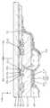
도 1은 본 발명의 일 실시예에 관한 유기발광 디스플레이 장치를 개략적으로 도시하는 단면도이다.
도 2는 본 발명의 다른 일 실시예에 관한 유기발광 디스플레이 장치를 개략적으로 도시하는 단면도이다.
도 3은 본 발명의 또 다른 일 실시예에 관한 유기발광 디스플레이 장치를 개략적으로 도시하는 단면도이다.
도 4 내지 도 6은 본 발명의 유기발광 디스플레이 장치를 제조하는 제조 공정을 개략적으로 도시하는 단면도들이다.1 is a schematic cross-sectional view of an organic light emitting display device according to an embodiment of the present invention.
2 is a schematic cross-sectional view of an organic light emitting display device according to another embodiment of the present invention.
3 is a cross-sectional view schematically showing an organic light emitting display device according to another embodiment of the present invention.
4 to 6 are cross-sectional views schematically showing a manufacturing process for manufacturing the organic light emitting display device of the present invention.
본 발명은 다양한 변환을 가할 수 있고 여러 가지 실시예를 가질 수 있는 바, 특정 실시예들을 도면에 예시하고 상세한 설명에 상세하게 설명하고자 한다. 본 발명의 효과 및 특징, 그리고 그것들을 달성하는 방법은 도면과 함께 상세하게 후술되어 있는 실시예들을 참조하면 명확해질 것이다. 그러나 본 발명은 이하에서 개시되는 실시예들에 한정되는 것이 아니라 다양한 형태로 구현될 수 있다.Since the present invention can apply various transformations and have various embodiments, specific embodiments are illustrated in the drawings and will be described in detail in the detailed description. Effects and features of the present invention, and a method of achieving them will be apparent with reference to the embodiments described later in detail together with the drawings. However, the present invention is not limited to the embodiments disclosed below and may be implemented in various forms.
이하, 첨부된 도면을 참조하여 본 발명의 실시예들을 상세히 설명하기로 하며, 도면을 참조하여 설명할 때 동일하거나 대응하는 구성 요소는 동일한 도면부호를 부여하고 이에 대한 중복되는 설명은 생략하기로 한다.Hereinafter, embodiments of the present invention will be described in detail with reference to the accompanying drawings, and when describing with reference to the drawings, the same or corresponding constituent elements are assigned the same reference numerals, and redundant descriptions thereof will be omitted. .
이하의 실시예에서, 제1, 제2 등의 용어는 한정적인 의미가 아니라 하나의 구성 요소를 다른 구성 요소와 구별하는 목적으로 사용되었다. 또한, 단수의 표현은 문맥상 명백하게 다르게 뜻하지 않는 한, 복수의 표현을 포함한다.In the following embodiments, terms such as first and second are not used in a limiting meaning, but for the purpose of distinguishing one component from another component. In addition, expressions in the singular include plural expressions unless the context clearly indicates otherwise.
한편, 포함하다 또는 가지다 등의 용어는 명세서상에 기재된 특징, 또는 구성요소가 존재함을 의미하는 것이고, 하나 이상의 다른 특징들 또는 구성요소가 부가될 가능성을 미리 배제하는 것은 아니다. 또한, 막, 영역, 구성 요소 등의 부분이 다른 부분 "위에" 또는 "상에" 있다고 할 때, 다른 부분의 "바로 위에" 또는 "바로 상에" 있는 경우뿐만 아니라, 그 중간에 다른 막, 영역, 구성 요소 등이 개재되어 있는 경우도 포함한다.Meanwhile, terms such as include or have means that the features or components described in the specification are present, and do not preclude the possibility of adding one or more other features or components in advance. In addition, when a part such as a film, region, component, etc. is said to be "on" or "on" another part, not only is it "immediately" or "immediately" of another part, as well as another film in the middle, It also includes a case where a region, a component, etc. are interposed.
도면에서는 설명의 편의를 위하여 구성 요소들이 그 크기가 과장 또는 축소될 수 있다. 예컨대, 도면에서 나타난 각 구성의 크기 및 두께는 설명의 편의를 위해 임의로 나타내었으므로, 본 발명이 반드시 도시된 바에 한정되지 않는다.In the drawings, components may be exaggerated or reduced in size for convenience of description. For example, the size and thickness of each component shown in the drawings are arbitrarily shown for convenience of description, and the present invention is not necessarily limited to what is shown.
x축, y축 및 z축은 직교 좌표계 상의 세 축으로 한정되지 않고, 이를 포함하는 넓은 의미로 해석될 수 있다. 예를 들어, x축, y축 및 z축은 서로 직교할 수도 있지만, 서로 직교하지 않는 서로 다른 방향을 지칭할 수도 있다.The x-axis, y-axis, and z-axis are not limited to three axes on a Cartesian coordinate system, and can be interpreted in a broad sense including them. For example, the x-axis, y-axis, and z-axis may be orthogonal to each other, but may refer to different directions that are not orthogonal to each other.
어떤 실시예가 달리 구현 가능한 경우에 특정한 공정 순서는 설명되는 순서와 다르게 수행될 수도 있다. 예를 들어, 연속하여 설명되는 두 공정이 실질적으로 동시에 수행될 수도 있고, 설명되는 순서와 반대의 순서로 진행될 수 있다.When a certain embodiment can be implemented differently, a specific process order may be performed differently from the described order. For example, two processes described in succession may be performed substantially simultaneously, or may be performed in an order opposite to the described order.
도 1은 본 발명의 일 실시예에 관한 유기발광 디스플레이 장치를 개략적으로 도시하는 단면도이다.1 is a schematic cross-sectional view of an organic light emitting display device according to an embodiment of the present invention.
도 1을 참조하면, 본 발명의 일 실시예에 관한 유기발광 디스플레이 장치는 하부기판(100)과, 하부기판(100) 상에 배치된 복수개의 제1박막트랜지스터(TFT1)들 및 복수개의 제2박막트랜지스터(TFT2)들과, 제1절연층(170), 배리어층(300), 밀봉부재(400) 및 상부기판(500)을 구비한다.Referring to FIG. 1, an organic light emitting display device according to an embodiment of the present invention includes a
하부기판(100)은 디스플레이영역(DA)과 이 디스플레이영역(DA) 외곽의 주변영역(PA)을 갖는다. 디스플레이영역(DA)은 유기발광소자(200)들이 배치되는 영역이고, 디스플레이영역(DA) 외곽의 주변영역(PA)은 디스플레이가 이루어지지 않는 데드 스페이스(dead space)로서, 디스플레이영역(DA)에 전기적 신호를 인가하는 구동부 등은 이러한 주변영역(PA)에 위치할 수 있다. 하부기판(100)은 글라스재, 금속재, 또는 PET(Polyethylen terephthalate), PEN(Polyethylen naphthalate), 폴리이미드(Polyimide) 등과 같은 플라스틱재 등, 다양한 재료로 형성된 것일 수 있다. 이는 후술하는 상부기판(500)의 경우도 동일한 재료로 형성될 수 있다.The
하부기판(100)의 디스플레이영역(DA)에는 복수개의 제1박막트랜지스터(TFT1)들이 배치되는데, 복수개의 제1박막트랜지스터(TFT1)들 외에 복수개의 제1박막트랜지스터(TFT1)들에 전기적으로 연결되는 복수개의 유기발광소자(200)들이 배치될 수 있다. 유기발광소자(200)들이 제1박막트랜지스터(TFT1)들에 전기적으로 연결된다는 것은, 복수개의 화소전극(210)들이 복수개의 제1박막트랜지스터(TFT1)들에 전기적으로 연결되는 것으로 이해될 수 있다.A plurality of first thin film transistors TFT1 are disposed in the display area DA of the
물론 하부기판(100)의 주변영역(PA)에도 복수개의 제2박막트랜지스터(TFT2)들이 배치될 수 있다. 이러한 제2박막트랜지스터(TFT2)들은 예컨대 디스플레이영역(DA) 내에 인가되는 전기적 신호를 제어하기 위한 구동부의 일부일 수 있다.Of course, a plurality of second thin film transistors TFT2 may be disposed in the peripheral area PA of the
이러한 제1박막트랜지스터(TFT1)들이나 제2박막트랜지스터(TFT2)들은 비정질실리콘, 다결정실리콘 또는 유기반도체물질을 포함하는 반도체층(120), 게이트전극(140), 소스전극(162) 및 드레인전극(160)을 포함한다. 하부기판(100) 상에는 하부기판(100)의 면을 평탄화하기 위해 또는 반도체층(120)으로 불순물 등이 침투하는 것을 방지하기 위해, 실리콘옥사이드 또는 실리콘나이트라이드 등으로 형성된 버퍼층(110)이 배치되고, 이 버퍼층(110) 상에 반도체층(120)이 위치하도록 할 수 있다.These first thin film transistors TFT1 or second thin film transistors TFT2 include a
반도체층(120)의 상부에는 게이트전극(140)이 배치되는데, 이 게이트전극(140)에 인가되는 신호에 따라 소스전극(162) 및 드레인전극(160)이 전기적으로 소통된다. 게이트전극(140)은 인접층과의 밀착성, 적층되는 층의 표면 평탄성 그리고 가공성 등을 고려하여, 예컨대 알루미늄(Al), 백금(Pt), 팔라듐(Pd), 은(Ag), 마그네슘(Mg), 금(Au), 니켈(Ni), 네오디뮴(Nd), 이리듐(Ir), 크롬(Cr), 리튬(Li), 칼슘(Ca), 몰리브덴(Mo), 티타늄(Ti), 텅스텐(W), 구리(Cu) 중 하나 이상의 물질로 단층 또는 다층으로 형성될 수 있다. 이때 반도체층(120)과 게이트전극(140)과의 절연성을 확보하기 위하여, 실리콘옥사이드 및/또는 실리콘나이트라이드 등으로 형성되는 게이트절연막(130)이 반도체층(120)과 게이트전극(140) 사이에 개재될 수 있다.A
게이트전극(140)의 상부에는 층간절연막(150)이 배치될 수 있는데, 이는 실리콘옥사이드 또는 실리콘나이트라이드 등의 물질로 단층으로 형성되거나 또는 다층으로 형성될 수 있다.An interlayer insulating
층간절연막(150)의 상부에는 소스전극(162) 및 드레인전극(160)이 배치된다. 소스전극(162) 및 드레인전극(160)은 층간절연막(150)과 게이트절연막(130)에 형성되는 컨택홀을 통하여 반도체층(120)에 각각 전기적으로 연결된다. 소스전극(162) 및 드레인전극(160)은 도전성 등을 고려하여 예컨대 알루미늄(Al), 백금(Pt), 팔라듐(Pd), 은(Ag), 마그네슘(Mg), 금(Au), 니켈(Ni), 네오디뮴(Nd), 이리듐(Ir), 크롬(Cr), 리튬(Li), 칼슘(Ca), 몰리브덴(Mo), 티타늄(Ti), 텅스텐(W), 구리(Cu) 중 하나 이상의 물질로 단층 또는 다층으로 형성될 수 있다.A
이러한 구조의 제1박막트랜지스터(TFT1)들 및/또는 제2박막트랜지스터(TFT2)들 상에는 필요에 따라 제1박막트랜지스터(TFT1)들 및/또는 제2박막트랜지스터(TFT2)들을 덮는 보호막(미도시)이 배치될 수도 있다. 보호막(미도시)은 예컨대 실리콘옥사이드, 실리콘나이트라이드 또는 실리콘옥시나이트라이드 등과 같은 무기물로 형성될 수 있다.On the first thin film transistors TFT1 and/or the second thin film transistors TFT2 having such a structure, a protective film (not shown) covering the first thin film transistors TFT1 and/or the second thin film transistor TFT2 as necessary. ) May be placed. The protective film (not shown) may be formed of an inorganic material such as silicon oxide, silicon nitride, or silicon oxynitride.
보호막(미도시) 상에는 제1절연층(170)이 배치될 수 있다. 이 경우 제1절연층(170)은 평탄화막일 수도 있고 보호막일 수도 있다. 예컨대 도 1에 도시된 것과 같이 제1박막트랜지스터(TFT1)들 상부에 유기발광소자(200)들이 배치될 경우 제1박막트랜지스터(TFT1)들의 상면을 대체로 평탄화하기 위한 평탄화막으로서 제1절연층(170)이 배치될 수 있다. 이러한 제1절연층(170)은 예컨대 아크릴계 유기물 또는 BCB(Benzocyclobutene) 등으로 형성될 수 있다. 도 1에서는 제1절연층(170) 이 단층으로 도시되어 있으나, 다층일 수도 있는 등 다양한 변형이 가능하다.A first insulating
하부기판(100)의 디스플레이영역(DA) 내에 있어서, 제1절연층(170) 상에는, 복수개의 화소전극(210)들, 화소전극(210)들에 대향하는 대향전극(230) 및 그 사이에 개재되며 발광층을 포함하는 중간층(220)을 갖는 유기발광소자(200)들이 배치된다.In the display area DA of the
제1절연층(170)에는 제1박막트랜지스터(TFT1)들의 소스전극(162) 및 드레인전극(160) 중 적어도 어느 하나를 노출시키는 개구부가 존재하며, 이 개구부를 통해 소스전극(162) 및 드레인전극(160) 중 어느 하나와 컨택하여 제1박막트랜지스터(TFT1)들과 전기적으로 연결되는 복수개의 화소전극(210)들이 제1절연층(170) 상에 배치된다. 화소전극(210)들은 (반)투명 전극 또는 반사형 전극으로 형성될 수 있다. (반)투명 전극으로 형성될 때에는 예컨대 ITO, IZO, ZnO, In2O3, IGO 또는 AZO로 형성될 수 있다. 반사형 전극으로 형성될 때에는 Ag, Mg, Al, Pt, Pd, Au, Ni, Nd, Ir, Cr 및 이들의 화합물 등으로 형성된 반사막과, ITO, IZO, ZnO, In2O3, IGO 또는 AZO로 형성된 층을 가질 수 있다. 물론 본 발명이 이에 한정되는 것은 아니고 다양한 재질로 형성될 수 있으며, 그 구조 또한 단층 또는 다층이 될 수 있는 등 다양한 변형이 가능하다.The first insulating
제1절연층(170) 상부에는 제2절연층(180)이 배치될 수 있다. 이 제2절연층(180)은 화소정의막으로서, 각 부화소들에 대응하는 개구들, 즉 복수개의 화소전극(210)들의 가장자리를 덮으며 각각의 적어도 중앙부가 노출되도록 하는 개구들을 가짐으로써 화소를 정의하는 역할을 한다. 또한, 도 1에 도시된 바와 같이, 제2절연층(180)은 화소전극(210)들의 단부와 화소전극(210)들 상부에 배치된 대향전극(230)과의 사이의 거리를 증가시킴으로써 화소전극(210)들의 단부에서 아크가 발생하는 것을 방지하는 역할을 한다. 이와 같은 제2절연층(180)은 예컨대 폴리이미드 등과 같은 유기물로 형성될 수 있다.A second insulating
상술한 것처럼 화소정의막으로 이해될 수 있는 제2절연층(180)은 화소영역을 정의하며 하부기판(100)의 디스플레이영역(DA)에 배치될 수 있다. 이때 도1에 도시된 것과 같이 제2절연층(180)은 하부기판(100)의 디스플레이영역(DA) 외곽의 주변영역(PA)까지 확장해서 배치될 수 있다. 이에 대해서는 자세히 후술하기로 한다.As described above, the second insulating
유기발광소자(200)의 중간층(220)은 저분자 또는 고분자 물질을 포함할 수 있다. 저분자 물질을 포함할 경우 홀 주입층(HIL: Hole Injection Layer), 홀 수송층(HTL: Hole Transport Layer), 발광층(EML: Emission Layer), 전자 수송층(ETL: Electron Transport Layer), 전자 주입층(EIL: Electron Injection Layer) 등이 단일 혹은 복합의 구조로 적층되어 형성될 수 있으며, 사용 가능한 유기 재료도 구리 프탈로시아닌(CuPc: copper phthalocyanine), N,N-디(나프탈렌-1-일)-N,N'-디페닐-벤지딘 (N,N'-Di(naphthalene-1-yl)-N,N'-diphenyl-benzidine: NPB) , 트리스-8-하이드록시퀴놀린 알루미늄(tris-8-hydroxyquinoline aluminum)(Alq3) 등을 비롯해 다양한 물질이 사용될 수 있다. 이러한 층들은 진공증착 등의 방법으로 형성될 수 있다.The
중간층(220)이 고분자 물질을 포함할 경우에는 대개 홀 수송층(HTL) 및 발광층(EML)을 포함하는 구조를 가질 수 있다. 이 때, 홀 수송층으로 PEDOT를 사용하고, 발광층으로PPV(Poly-Phenylenevinylene)계 및 폴리플루오렌(Polyfluorene)계 등 고분자 물질을 사용하며, 이를 스크린 인쇄나 잉크젯 인쇄방법, 레이저열전사방법(LITI; Laser induced thermal imaging) 등으로 형성할 수 있다. 물론 중간층(220)은 반드시 이에 한정되는 것은 아니고, 다양한 구조를 가질 수도 있음은 물론이다.When the
대향전극(230)은 디스플레이영역(DA)과 주변영역(PA) 상부 전면(全面)에 걸쳐 배치되는데, 도 1에 도시된 것과 같이 디스플레이영역(DA)과 주변영역(PA)의 적어도 일부분을 덮도록 배치될 수 있다. 즉, 대향전극(230)은 복수개의 유기발광소자(200)들에 있어서 일체(一體)로 형성되어 복수개의 화소전극(210)들에 대응할 수 있다.The
대향전극(230)은 (반)투명 전극 또는 반사형 전극으로 형성될 수 있다. 대향전극(230)이 (반)투명 전극으로 형성될 때에는 일함수가 작은 금속 즉, Li, Ca, LiF/Ca, LiF/Al, Al, Ag, Mg 및 이들의 화합물로 형성된 층과 ITO, IZO, ZnO 또는 In2O3 등의 (반)투명 도전층을 가질 수 있다. 대향전극(230)이 반사형 전극으로 형성될 때에는Li, Ca, LiF/Ca, LiF/Al, Al, Ag, Mg 및 이들의 화합물로 형성된 층을 가질 수 있다. 물론 대향전극(230)의 구성 및 재료가 이에 한정되는 것은 아니며 다양한 변형이 가능함은 물론이다.The
한편, 하부기판(100)의 주변영역(PA) 상에는 밀봉부재(400)가 배치될 수 있다. 밀봉부재(400)를 통해 상부기판(500)을 하부기판(100)에 접합하여 밀봉시킬 수 있다. 이러한 밀봉부재(400)는 프릿(frit) 또는 에폭시 등으로 형성할 수 있는데, 물론 본 발명이 이에 한정되는 것은 아니다.Meanwhile, the sealing
이러한 밀봉부재(400)는 도 1에 도시된 것과 같이, 적어도 일부분이 제1절연층(170)에 중첩되도록 배치될 수 있다. 밀봉부재(400)의 적어도 일부분이 제1절연층(170)에 중첩된다는 것은, 밀봉부재(400)가 하부기판(100)의 에지(edge) 방향(-x방향)과 반대되는 방향(+x방향) 즉 디스플레이영역(DA) 측에 가깝게 배치되는 것으로 이해될 수 있다. 밀봉부재(400)가 디스플레이영역(DA) 측에 가깝게 배치됨에 따라 밀봉부재(400)가 배치되는 하부기판(100)의 주변영역(PA)의 폭이 줄어들게 된다. 따라서 본 발명의 일 실시예의 유기발광 디스플레이 장치의 데드 스페이스를 줄일 수 있다.As shown in FIG. 1, the sealing
다만, 밀봉부재(400)가 디스플레이 영역 측에 가깝게 배치되기 위해서는 상술한 것과 같이 밀봉부재(400)의 적어도 일부분이 제1절연층(170)에 중첩되도록 배치될 수 있다. 이 경우 밀봉부재(400)를 통해 상부기판(500)과 하부기판(100)을 접합시키는 과정에서 밀봉부재(400)에 가해지는 열로 인해 하부기판(100)의 주변영역(PA)에 배치된 제1절연층(170)과 이러한 제1절연층(170) 하부에 배치된 제2박막트랜지스터(TFT2)들이 손상되는 문제점이 발생할 수 있다. 이러한 문제점을 해결하기 위해 후술하는 하부기판(100)의 주변영역(PA)에 배치된 제1절연층(170)과 밀봉부재(400) 사이에 배리어층(300)이 개재될 수 있다.However, in order for the sealing
배리어층(300)은 도 1에 도시된 것과 같이, 하부기판(100)의 주변영역(PA) 상에 배치된 복수개의 제2박막트랜지스터들을 덮도록 배치된 제1절연층(170) 상에 배치될 수 있다. 배리어층(300)은 하부기판(100)의 에지 방향(-x방향)과 하부기판(100)의 에지 방향의 반대 방향(+x방향)으로 연장되어 배치될 수 있는 등 다양한 변형이 가능하다. 단, 이 경우에도 배리어층(300)은 하부기판(100)의 주변영역(PA) 상에 배치된 제1절연층(170) 중 밀봉부재(400)가 중첩되어 배치된 부분과 그러한 밀봉부재(400) 사이에는 반드시 개재되도록 배치된다.The
이러한 배리어층(300)은 무기절연물을 포함할 수 있다. 예컨대 배리어층(300)은 실리콘나이트라이드 또는 실리콘옥사이드 등으로 형성될 수 있으나 본 발명이 반드시 이에 한정되는 것은 아니다.The
한편, 층간절연막(150) 상에는 배선라인(165)이 배치될 수 있다. 배선라인(165)은 하부기판(100)의 주변영역(PA) 상에 배치되며 유기발광소자의 대향전극에 전기적으로 연결되도록 배치될 수 있다. 도 1에는 배선라인(165)이 층간절연막(150) 상에 배치된 것으로 도시되어 있으나, 배선라인(165)은 박막트랜지스터(TFT1, TFT2)들이 포함하는 전극들 중 어느 하나와 동일층에 위치할 수 있다. 예컨대 배선라인(165)은 복수개의 박막트랜지스터들(TFT1, TFT2)이 포함하는 전극들 중 소스전극(162) 및 드레인전극(160)과 동일층에 위치할 수 있다. 이 경우 배선라인(165)은 제조과정에서 소스전극(162) 및 드레인전극(160)과 동일물질로 동시에 형성될 수 있다.Meanwhile, a
이와 같이 밀봉부재(400)와 제1절연층(170) 사이에 개재된 배리어층(300)을 통해, 밀봉부재(400)를 디스플레이영역(DA)에 가깝게 배치함에 따라 상부기판(500)과 하부기판(100)을 밀봉하는 과정에서 발생된 열이 밀봉부재(400)를 통해 하부기판(100)의 주변영역(PA)에 배치된 소자들을 손상시키는 것을 방지하여, 유기발광 디스플레이 장치의 데드 스페이스를 획기적으로 감소시킬 수 있다.In this way, through the
도 2는 본 발명의 다른 일 실시예에 관한 유기발광 디스플레이 장치를 개략적으로 도시하는 단면도이다.2 is a schematic cross-sectional view of an organic light emitting display device according to another embodiment of the present invention.
도 2를 참조하면, 본 발명의 다른 일 실시예에 관한 유기발광 디스플레이 장치는 하부기판(100)과, 하부기판(100) 상에 배치된 복수개의 1박막트랜지스터(TFT1)들 및 복수개의 제2박막트랜지스터(TFT2)들과, 배선라인(165), 제1절연층(170), 배리어층(300), 밀봉부재(400) 및 상부기판(500)을 구비한다. 도 2에 도시된 본 발명의 다른 일 실시예에 관한 유기발광 디스플레이 장치의 설명 중 도 1에서 전술한 내용과 중복되는 내용은 생략하고 설명하기로 한다.Referring to FIG. 2, an organic light emitting display device according to another embodiment of the present invention includes a
본 발명의 다른 일 실시예에 관한 유기발광 디스플레이 장치의 하부기판(100)의 주변영역(PA) 상에는 밀봉부재(400)가 배치될 수 있다. 밀봉부재(400)를 통해 상부기판(500)을 하부기판(100)에 접합하여 밀봉시킬 수 있다. 이러한 밀봉부재(400)는 프릿(frit) 또는 에폭시 등으로 형성할 수 있는데, 물론 본 발명이 이에 한정되는 것은 아니다.The sealing
이러한 밀봉부재(400)는 도 1에 도시된 것과 같이, 적어도 일부분이 제1절연층(170)에 중첩되도록 배치될 수 있다. 밀봉부재(400)의 적어도 일부분이 제1절연층(170)에 중첩된다는 것은, 밀봉부재(400)가 하부기판(100)의 에지(edge) 방향(-x방향)과 반대되는 방향(+x방향) 즉 디스플레이영역(DA) 측에 가깝게 배치되는 것으로 이해될 수 있다. 밀봉부재(400)가 디스플레이 영역 측에 가깝게 배치됨에 따라 밀봉부재(400)가 배치되는 하부기판(100)의 주변영역(PA)의 폭이 줄어들게 된다. 따라서 본 발명의 일 실시예의 유기발광 디스플레이 장치의 데드 스페이스를 줄일 수 있다.As shown in FIG. 1, the sealing
다만, 밀봉부재(400)가 디스플레이 영역 측에 가깝게 배치되기 위해서는 상술한 것과 같이 밀봉부재(400)의 적어도 일부분이 제1절연층(170)에 중첩되도록 배치될 수 있다. 이 경우 밀봉부재(400)를 통해 상부기판(500)과 하부기판(100)을 접합시키는 과정에서 밀봉부재(400)에 가해지는 열로 인해 하부기판(100)의 주변영역(PA)에 배치된 제1절연층(170)과 이러한 제1절연층(170) 하부에 배치된 제2박막트랜지스터(TFT2)들이 손상되는 문제점이 발생할 수 있다. 이러한 문제점을 해결하기 위해 후술하는 하부기판(100)의 주변영역(PA)에 배치된 제1절연층(170)과 밀봉부재(400) 사이에 배리어층(300)이 개재될 수 있다.However, in order for the sealing
배리어층(300)은 도 1에 도시된 것과 같이, 하부기판(100)의 주변영역(PA) 상에 배치된 복수개의 제2박막트랜지스터들을 덮도록 배치된 제1절연층(170) 상에 배치될 수 있다. 배리어층(300)은 하부기판(100)의 에지 방향(-x방향)과 하부기판(100)의 에지 방향의 반대 방향(+x방향)으로 연장되어 배치될 수 있는 등 다양한 변형이 가능하다. 단, 이 경우에도 배리어층(300)은 하부기판(100)의 주변영역(PA) 상에 배치된 제1절연층(170) 중 밀봉부재(400)가 중첩되어 배치된 부분과 그러한 밀봉부재(400) 사이에는 반드시 개재되도록 배치된다.The
이러한 배리어층(300)은 무기절연물을 포함할 수 있다. 예컨대 배리어층(300)은 실리콘나이트라이드 또는 실리콘옥사이드 등으로 형성될 수 있으나 본 발명이 반드시 이에 한정되는 것은 아니다.The
한편, 본 발명의 다른 일 실시예에 관한 유기발광 디스플레이 장치는 하부기판(100)의 에지(edge) 방향으로 연장되어 배치되는 배선라인(165)을 포함한다. 이러한 배선라인(165)은 하부기판(100)의 주변영역(PA) 상에 배치되며 유기발광소자의 대향전극에 전기적으로 연결되도록 배치될 수 있다.Meanwhile, the organic light emitting display device according to another exemplary embodiment of the present invention includes a
도 2에는 배선라인(165)이 층간절연막(150) 상에 배치된 것으로 도시되어 있으나, 배선라인(165)은 박막트랜지스터(TFT1, TFT2)들이 포함하는 전극들 중 어느 하나와 동일층에 위치할 수 있다. 예컨대 배선라인(165)은 복수개의 박막트랜지스터들(TFT1, TFT2)이 포함하는 전극들 중 소스전극(162) 및 드레인전극(160)과 동일층에 위치할 수 있다. 이 경우 배선라인(165)은 제조과정에서 소스전극(162) 및 드레인전극(160)과 동일물질로 동시에 형성될 수 있다. 따라서 배선라인(165)은 예컨대 알루미늄(Al), 백금(Pt), 팔라듐(Pd), 은(Ag), 마그네슘(Mg), 금(Au), 니켈(Ni), 네오디뮴(Nd), 이리듐(Ir), 크롬(Cr), 리튬(Li), 칼슘(Ca), 몰리브덴(Mo), 티타늄(Ti), 텅스텐(W), 구리(Cu) 중 하나 이상의 물질로 단층 또는 다층으로 형성될 수 있다.Although the
이러한 배선라인(165)이 하부기판(100)의 에지(edge) 방향으로 연장되어 배치됨에 따라, 금속물질을 포함하여 형성되는 배선라인(165)의 폭(w)이 넓어지게 된다. 배선라인(165)의 연장된 단부의 적어도 일부는 밀봉부재(400)와 중첩되지 않을 수 있다. 따라서 밀봉부재(400)를 통해 하부기판(100)과 상부기판(500)을 접합하는 과정에서 밀봉부재(400)를 통해 제1절연층(170)이나 제1절연층(170) 하부 배치된 제2박막트랜지스터(TFT2)들에 전달되는 열을 이러한 배선라인(165)의 연장된 단부를 통해 외부로 배출시키는 것이 더욱 용이하다.As the
전술한 것과 같이, 밀봉부재(400)와 제1절연층(170) 사이에는 배리어층(300)이 개재될 수 있는데, 이러한 배리어층(300)은 배선라인(165)이 하부기판(100)의 에지 방향으로 연장되어 배치됨에 따라 배선라인(165)의 연장된 단부의 적어도 일부분을 노출시킬 수 있다. 따라서 배리어층(300)이 배치되지 않아 외부로 노출된 배선라인(165)의 연장된 단부를 통해 밀봉부재(400)로 전달된 열을 외부로 배출시키는 것이 더욱 용이해질 수 있다.As described above, a
도 3은 본 발명의 또 다른 일 실시예에 관한 유기발광 디스플레이 장치를 개략적으로 도시하는 단면도이다.3 is a cross-sectional view schematically showing an organic light emitting display device according to another embodiment of the present invention.
도 3을 참조하면, 본 발명의 또 다른 일 실시예에 관한 유기발광 디스플레이 장치는 하부기판(100)과, 하부기판(100) 상에 배치된 복수개의 제1박막트랜지스터(TFT1)들 및 복수개의 제2박막트랜지스터(TFT2)들과, 제1절연층(170), 제2절연층(180), 배리어층(300), 밀봉부재(400) 및 상부기판(500)을 구비한다. 도 2에 도시된 본 발명의 다른 일 실시예에 관한 유기발광 디스플레이 장치의 설명 중 도 1에서 전술한 내용과 중복되는 내용은 생략하고 설명하기로 한다.3, an organic light emitting display device according to another embodiment of the present invention includes a
본 발명의 또 다른 일 실시예에 관한 유기발광 디스플레이 장치는 하부기판(100)의 디스플레이영역(DA) 상에 제1박막트랜지스터(TFT1)들이 배치되고, 하부기판(100)의 주변영역(PA) 상에 제2박막트랜지스터(TFT2)들이 배치될 수 있다.In the organic light emitting display device according to another embodiment of the present invention, the first thin film transistors TFT1 are disposed on the display area DA of the
이러한 박막트랜지스터(TFT1, TFT2)들을 덮도록제1절연층(170)이 배치될 수 있다. 이 경우 제1절연층(170)은 평탄화막일 수도 있고 보호막일 수도 있다. 제1절연층(170)은 예컨대 아크릴계 유기물 또는 BCB(Benzocyclobutene) 등으로 형성될 수 있다. 도 3에서는 제1절연층(170) 이 단층으로 도시되어 있으나, 다층일 수도 있는 등 다양한 변형이 가능하다.To cover these thin film transistors (TFT1, TFT2)The first insulating
하부기판(100)의 디스플레이영역(DA) 내에 있어서, 제1절연층(170) 상에는, 복수개의 화소전극(210)들, 화소전극(210)들에 대향하는 대향전극(230) 및 그 사이에 개재되며 발광층을 포함하는 중간층(220)을 갖는 유기발광소자(200)들이 배치된다.In the display area DA of the
제1절연층(170)에는 제1박막트랜지스터(TFT1)들의 소스전극(162) 및 드레인전극(160) 중 적어도 어느 하나를 노출시키는 개구부가 존재하며, 이 개구부를 통해 소스전극(162) 및 드레인전극(160) 중 어느 하나와 컨택하여 제1박막트랜지스터(TFT1)들과 전기적으로 연결되는 복수개의 화소전극(210)들이 제1절연층(170) 상에 배치된다.The first insulating
제2절연층(180)은 제1절연층(170) 상부에 배치될 수 있다. 상술한 것과 같이 하부기판(100)의 디스플레이영역(DA)에 배치된 제1절연층(170) 상에 배치된 제2절연층(180)은 화소정의막으로서, 각 부화소들에 대응하는 개구들, 즉 복수개의 화소전극(210)들의 가장자리를 덮으며 각각의 적어도 중앙부가 노출되도록 하는 개구들을 가짐으로써 화소를 정의하는 역할을 한다. 제2절연층(180)은 예컨대 폴리이미드 등과 같은 유기물로 형성될 수 있으나 반드시 이에 한정되는 것은 아니다.The second
본 발명의 또 다른 일 실시예에 관한 제2절연층(180)은 하부기판(100)의 주변영역(PA)에 배치된 제1절연층(170) 상에도 연장되어 배치될 수 있다. 도 3에서는 제2절연층(180)은 하부기판(100)의 주변영역(PA)에 배치된 제1절연층(170)의 단부를 덮는 것으로 도시되어 있으나 반드시 이에 한정되는 것은 아니다.The second
한편, 하부기판(100)의 주변영역(PA) 상에는 밀봉부재(400)가 배치될 수 있다. 밀봉부재(400)를 통해 상부기판(500)을 하부기판(100)에 접합하여 밀봉시킬 수 있다. 이러한 밀봉부재(400)는 프릿(frit) 또는 에폭시 등으로 형성할 수 있는데, 물론 본 발명이 이에 한정되는 것은 아니다.Meanwhile, the sealing
이러한 밀봉부재(400)는 도 3에 도시된 것과 같이, 적어도 일부분이 제1절연층(170)에 중첩되도록 배치될 수 있다. 밀봉부재(400)의 적어도 일부분이 제1절연층(170)에 중첩된다는 것은, 밀봉부재(400)가 하부기판(100)의 에지(edge) 방향(-x방향)과 반대되는 방향(+x방향) 즉 디스플레이영역(DA) 측에 가깝게 배치되는 것으로 이해될 수 있다. 밀봉부재(400)가 디스플레이 영역 측에 가깝게 배치됨에 따라 밀봉부재(400)가 배치되는 하부기판(100)의 주변영역(PA)의 폭이 줄어들게 된다. 따라서 본 발명의 일 실시예의 유기발광 디스플레이 장치의 데드 스페이스를 줄일 수 있다.As illustrated in FIG. 3, the sealing
다만, 밀봉부재(400)가 디스플레이 영역 측에 가깝게 배치되기 위해서는 상술한 것과 같이 밀봉부재(400)의 적어도 일부분이 제1절연층(170)에 중첩되도록 배치될 수 있다. 이 경우 밀봉부재(400)를 통해 상부기판(500)과 하부기판(100)을 접합시키는 과정에서 밀봉부재(400)에 가해지는 열로 인해 하부기판(100)의 주변영역(PA)에 배치된 제1절연층(170)과 이러한 제1절연층(170) 하부에 배치된 제2박막트랜지스터(TFT2)들이 손상되는 문제점이 발생할 수 있다. 이러한 문제점을 해결하기 위해 후술하는 하부기판(100)의 주변영역(PA)에 배치된 제1절연층(170) 상에 제2절연층(180)이 연장되어 배치하고, 상기 제2절연층(180) 상에 밀봉부재(400)를 배치할 수 있다.However, in order for the sealing
따라서 본 발명의 또 다른 일 실시예에 관한 밀봉부재(400)는 도 3에 도시된 것과 같이, 제2절연층(180)이 하부기판(100)의 주변영역(PA)에 배치된 부분 상에 배치될 수 있다. 밀봉부재(400)가 제2절연층(180) 상에 배치됨에 따라 밀봉부재(400)의 높이(h1)가 줄어들 수 있다. 다시 말해 종래에는 하부기판(100)과 상부기판(500) 사이에 밀봉부재가 배치되므로, 밀봉부재는 하부기판(100)과 상부기판(500) 사이의 거리(h1+h2)에 대응하는 높이로 배치되었다. 반면에 본 발명의 일 실시예에 따른 유기발광 디스플레이 장치에서는 제1절연층(170) 상에 배치된 제2절연층(180) 상에 밀봉부재(400)가 배치됨에 따라 제1절연층(170)과 제2절연층(180)의 높이(h2)만큼 밀봉부재(400)의 높이(h1)도 줄어들게 되는 것으로 이해될 수 있다. 따라서 밀봉부재의 높이(h1)가 줄어듦에 따라 상부기판(500)과 하부기판(100)을 접합하는 과정에서 밀봉부재(400)를 통해 발생되는 열용량을 줄일 수 있다.Therefore, in the sealing
또한, 하부기판(100)의 주변영역(PA)에 배치된 제2절연층(180)과 밀봉부재(400) 사이에 배리어층(300)이 개재될 수 있다. 배리어층(300)은 도 3에 도시된 것과 같이, 복수개의 제2박막트랜지스터(TFT2)들을 덮도록 배치된 제1절연층(170) 상에 배치된 제2절연층(180) 상에 배치될 수 있다. 배리어층(300)은 하부기판(100)의 에지 방향(-x방향)과 하부기판(100)의 에지 방향의 반대 방향(+x방향)으로 연장되어 배치될 수 있는 등 다양한 변형이 가능하다. 이러한 배리어층(300)은 무기절연물을 포함할 수 있다. 예컨대 배리어층(300)은 실리콘나이트라이드 또는 실리콘옥사이드 등으로 형성될 수 있으나 본 발명이 반드시 이에 한정되는 것은 아니다.In addition, the
상술한 것과 같이 높이가 낮아진 밀봉부재(400)를 통해 발생되는 열용량을 줄이고 동시에 밀봉부재(400)와 제2절연층(180) 사이에 개재되는 배리어층(300)을 통해 밀봉부재(400) 하부에 배치된 소자들로 전달되는 열을 차단함으로써, 유기발광 디스플레이 장치의 데드 스페이스를 줄임과 동시에 상부기판(500)과 하부기판(100)을 밀봉하는 동안 하부기판(100)의 주변영역(PA)에 배치된 소자부들이 열에 의해 손상되는 것을 획기적으로 방지할 수 있다.The lower portion of the sealing
지금까지는 유기발광 디스플레이 장치에 대해서만 주로 설명하였으나, 본 발명이 이에 한정되는 것은 아니다. 예컨대 이러한 유기발광 디스플레이 장치를 이용한 유기발광 디스플레이 장치 제조방법 역시 본 발명의 범위에 속한다고 할 것이다.Until now, only the organic light emitting display device has been mainly described, but the present invention is not limited thereto. For example, a method of manufacturing an organic light-emitting display device using such an organic light-emitting display device will also fall within the scope of the present invention.
도 4 내지 도 6은 본 발명의 유기발광 디스플레이 장치를 제조하는 제조 공정을 개략적으로 도시하는 단면도들이다.4 to 6 are cross-sectional views schematically showing a manufacturing process for manufacturing the organic light emitting display device of the present invention.
도 4를 참조하면, 디스플레이영역(DA)과 디스플레이영역(DA) 외곽의 주변영역(PA)을 갖는 하부기판(100)을 준비하는 단계를 거쳐, 디스플레이영역(DA)에 복수개의 제1박막트랜지스터(TFT1)들과, 주변영역(PA)에 복수개의 제2박막트랜지스터(TFT2)들을 형성하는 단계를 거칠 수 있다.Referring to FIG. 4, after preparing a
이때 복수개의 박막트랜지스터들(TFT1, TFT2)을 형성하는 단계는, 먼저 하부기판(100) 상에 버퍼층(110)을 형성한 후 버퍼층(110) 상에 반도체층(120)을 패터닝하는 단계를 거칠 수 있다. 반도체층(120)을 패터닝 한 후 반도체층(120) 상에 게이트절연막(130)을 적층하고 게이트절연막(130) 상에 게이트전극(140)을 패터닝하는 단계를 거칠 수 있다. 게이트절연막(130) 상에 반도체층(120)과 전기적으로 연결되는 소스전극(162) 및 드레인전극(160)을 패터닝 할 수 있다.In this case, the step of forming the plurality of thin film transistors TFT1 and TFT2 includes first forming the
한편, 복수개의 박막트랜지스터(TFT1, TFT2)들을 형성할 때, 박막트랜지스터(TFT1, TFT2)들과 박막트랜지스터(TFT1, TFT2)들이 포함하는 전극들 중 어느 하나와 동일층에 배선라인(165)을 동시에 형성할 수 있다. 도4에 도시된 것과 같이 배선라인(165)이 박막트랜지스터(TFT1, TFT2)들의 소스전극(162) 및 드레인전극(160)과 동일한 층에 동시에 형성될 수 있다. 다만 반드시 이에 한정되는 것은 아니고 다양한 변형이 가능하다.Meanwhile, when forming a plurality of thin film transistors (TFT1, TFT2), a
그 후, 박막트랜지스터(TFT1, TFT2)들 상에 보호막(미도시) 및 제1절연층(170)을 적층하는 단계를 거칠 수 있다. 보호막(미도시)은 복수개의 박막트랜지스터(TFT1, TFT2)들을 보호하는 보호막으로 이해될 수 있으며, 제1절연층(170)은 복수개의 박막트랜지스터들(TFT1, TFT2)을 보호하는 보호막 또는 제1절연층(170)의 상면을 대체로 평탄화하기 위한 평탄화막으로서 이해될 수 있다.Thereafter, a step of laminating a protective film (not shown) and a first insulating
제1절연층(170)과 층간절연막(150)에 컨택홀을 형성한 후 컨택홀을 통해 제1박막트랜지스터(TFT1)들의 소스전극(162) 및 드레인전극(160) 중 어느 하나와 전기적으로 연결되도록 복수개의 화소전극(210)들을 형성하는 단계를 거칠 수 있다. 이 경우 복수개의 화소전극(210)들은 디스플레이영역(DA)인 제1박막트랜지스터(TFT1)들 상에 형성될 수 있다.After forming a contact hole in the first insulating
그 후 도 5를 참조하면, 제1절연층(170) 상에 화소전극(210)들을 형성하고 난 후, 화소전극(210)들 상에 제2절연층(180)을 형성할 수 있다. 화소전극(210)들 상에 형성된 제2절연층(180)은 화소부를 정의하는 화소정의막의 역할을 한다. 이러한 제2절연층(180)은 복수개의 화소전극(210)들의 각각의 중앙부가 노출되도록 화소전극(210)들의 가장자리를 덮도록 형성될 수 있다.Thereafter, referring to FIG. 5, after forming the
이와 같이 제1절연층(170) 상에 제2절연층(180)을 형성하는 단계를 거친 후, 제2절연층(180)에 의해 노출된 화소전극(210)들의 중앙부 상에 발광층을 포함한 중간층(220)을 형성하는 단계를 거칠 수 있다. 그 후, 복수개의 화소전극(210)들과 대응되도록 대향전극(230)을 형성하는 단계를 더 거칠 수 있다. 예컨대 도 5에 도시된 것과 같이 대향전극(230)은 제2절연층(180) 전면(全面)에 걸쳐서 형성될 수 있다.After the step of forming the second insulating
대향전극(230)을 형성한 후 도 5에 도시된 것과 같이, 하부기판(100)의 주변영역(PA) 상에 형성된 제1절연층(170) 상의 적어도 일부에 배리어층(300)을 형성하는 단계를 거칠 수 있다. 이러한 배리어층(300)은 무기절연물로 형성될 수 있으며, 예컨대 실리콘옥사이드 또는 실리콘나이트라이드와 같은 절연물질로 형성될 수 있다. 배리어층(300)은 후술할 상부기판(500)과 하부기판(100)을 밀봉하는 단계에서 발생된 열이 밀봉부재(400)를 통해 하부에 배치된 제2박막트랜지스터(TFT2)들에 전달되어 소자들이 열에 의해 손상되는 것을 방지하는 역할을 할 수 있다.After forming the
그 후 도 6을 참조하면, 하부기판(100)의 주변영역(PA) 상에 밀봉부재(400)를 형성하는 단계를 거칠 수 있다. 이러한 밀봉부재(400)는 프릿(frit) 또는 에폭시 등으로 형성할 수 있는데, 물론 본 발명이 이에 한정되는 것은 아니다. 밀봉부재(400)는 하부기판(100)의 주변영역(PA) 상에 형성된 제1절연층(170)에 밀봉부재(400)의 적어도 일부분이 중첩되도록 하부기판(100)에 직접 형성할 수도 있고, 상부기판(500) 상에 이에 대응하는 위치에 형성할 수도 있다.Thereafter, referring to FIG. 6, a step of forming the sealing
밀봉부재(400)는 상술한 것과 같이, 적어도 일부분이 제1절연층(170)에 중첩되도록 형성될 수 있다. 밀봉부재(400)의 적어도 일부분이 제1절연층(170)에 중첩된다는 것은, 밀봉부재(400)가 하부기판(100)의 에지(edge) 방향(-x방향)과 반대되는 방향(+x방향) 즉 디스플레이영역(DA) 측에 가깝게 형성되는 것으로 이해될 수 있다. 밀봉부재(400)가 디스플레이 영역 측에 가깝게 형성됨에 따라 밀봉부재(400)가 형성되는 하부기판(100)의 주변영역(PA)의 폭이 줄어들게 된다. 따라서 본 발명의 일 실시예의 유기발광 디스플레이 장치의 데드 스페이스를 줄일 수 있다.As described above, the sealing
밀봉부재(400)를 형성한 후, 상부기판(500)과 하부기판(100)을 접합하여 밀봉부재(400)를 통해 밀봉하는 단계를 거칠 수 있다. 이때 도 6에 도시된 것과 같이 상부기판(500) 측에서 밀봉부재(400)에 레이저를 조사하여 상부기판(500)과 하부기판(100)을 접합시킬 수 있다. 이렇게 상부기판(500)과 하부기판(100)을 밀봉하는 과정에서 밀봉부재(400)에 가해지는 열로 인해 하부기판(100)의 주변영역(PA)에 배치된 제1절연층(170)과 이러한 제1절연층(170) 하부에 배치된 제2박막트랜지스터(TFT2)들과 같은 소자들이 손상되는 문제점이 발생한다. 이러한 문제점을 해결하기 위해 전술한 것과 같이 제1절연층(170)과 밀봉부재(400) 사이에 배리어층(300)을 형성하여 이러한 배리어층(300)이 밀봉부재(400)를 통해 열이 하부기판(100)의 주변영역(PA)에 배치된 소자들에 전달되어 손상되는 것을 획기적으로 방지한다.After the sealing
이와 함께 상부기판(500)과 하부기판(100)을 밀봉하는 과정에서 밀봉부재(400)에 가해지는 열로 인해 하부기판(100)의 주변영역(PA)에 배치된 제1절연층(170)과 이러한 제1절연층(170) 하부에 배치된 제2박막트랜지스터(TFT2)들과 같은 소자들이 손상되는 것을 더욱더 용이하게 방지하기 위해, 하부기판(100) 측에 온도 조절 장치(600)를 이용할 수 있다.In addition, the first insulating
온도 조절 장치(600)는 하부기판(100) 상에 배치된 하부막 및 소자들을 형성하는 재료들이 손상되는 온도 보다 낮은 온도로 하부기판(100)의 온도가 유지되도록 하부기판(100)의 온도를 조절하는 역할을 할 수 있다. 예컨대 실제로 열에 취약한 재료들 중 하나인 폴리이미드의 유리전이온도(Tg)는 약 400℃ 이므로, 하부기판(100)의 온도를 상온까지 낮출 필요 없이 적정한 온도 선에서 컨트롤하는 것 만으로도 충분한 효과를 기대할 수 있다. 따라서 공정조건이 간단하며 저비용으로 본 발명에 따른 유기발광 디스플레이 장치를 제조할 수 있어, 획기적으로 데드 스페이스가 줄어든 유기발광 디스플레이 장치를 구현할 수 있다.The
예컨대, 도 6에 도시된 것과 같이 하부기판(100)의 하부에 온도 조절 장치(600)가 배치되고, 온도 조절 장치(600)에서 하부기판(100)으로 냉기가 배출됨으로써 하부기판(100) 및 하부기판(100) 상에 배치된 박막 및 소자들이 손상될 정도로 온도가 오르는 것을 방지할 수 있다.For example, as shown in FIG. 6, a
본 발명은 도면에 도시된 실시예를 참고로 설명되었으나 이는 예시적인 것에 불과하며, 당해 기술분야에서 통상의 지식을 가진 자라면 이로부터 다양한 변형 및 균등한 다른 실시예가 가능하다는 점을 이해할 것이다. 따라서 본 발명의 진정한 기술적 보호 범위는 첨부된 특허청구범위의 기술적 사상에 의하여 정해져야 할 것 이다.The present invention has been described with reference to the embodiments shown in the drawings, but these are merely exemplary, and those of ordinary skill in the art will appreciate that various modifications and equivalent other embodiments are possible therefrom. Therefore, the true technical protection scope of the present invention should be determined by the technical spirit of the appended claims.
100: 하부기판 165: 배선라인
170: 제1절연층 180: 제2절연층
200: 유기발광소자 210: 화소전극
220: 중간층 230: 대향전극
300: 배리어층 400: 밀봉부재
500: 상부기판 600: 온도 조절 장치100: lower substrate 165: wiring line
170: first insulating layer 180: second insulating layer
200: organic light emitting device 210: pixel electrode
220: intermediate layer 230: counter electrode
300: barrier layer 400: sealing member
500: upper substrate 600: temperature control device
Claims (16)
Translated fromKorean상기 하부기판의 디스플레이 영역 상에 배치된 복수개의 제1박막트랜지스터들;
상기 제1박막트랜지스터들을 덮으며 상기 하부기판의 디스플레이 영역 및 상기 하부기판의 주변영역의 적어도 일부에 배치되며, 상기 하부기판의 가장자리를 향해 배치된 측면을 갖는, 제1절연층;
상기 제1박막트랜지스터들에 전기적으로 연결된 복수개의 유기발광소자들;
상기 제1절연층의 상기 측면을 커버하도록 적어도 일부분이 상기 제1절연층에 중첩하여 배치된, 밀봉부재;
상기 제1절연층과 상기 밀봉부재 사이에 개재된, 배리어층; 및
상기 하부기판에 대응하는 상부기판;
을 구비하는, 유기발광 디스플레이 장치.A lower substrate having a display area and a peripheral area outside the display area;
A plurality of first thin film transistors disposed on the display area of the lower substrate;
A first insulating layer covering the first thin film transistors, disposed in at least a portion of a display area of the lower substrate and a peripheral area of the lower substrate, and having a side surface disposed toward an edge of the lower substrate;
A plurality of organic light emitting devices electrically connected to the first thin film transistors;
A sealing member, at least partially overlapping the first insulating layer so as to cover the side surface of the first insulating layer;
A barrier layer interposed between the first insulating layer and the sealing member; And
An upper substrate corresponding to the lower substrate;
Having, an organic light emitting display device.
상기 하부기판의 주변영역 상에 배치된 복수개의 제2박막트랜지스터들을 더 포함하고, 상기 배리어층은 상기 제2박막트랜지스터들을 덮도록 배치된 상기 제1절연층 상에 배치되는, 유기발광 디스플레이 장치.The method of claim 1,
An organic light-emitting display device, further comprising a plurality of second thin film transistors disposed on a peripheral area of the lower substrate, wherein the barrier layer is disposed on the first insulating layer disposed to cover the second thin film transistors.
상기 배리어층은 무기절연물을 포함하는, 유기발광 디스플레이 장치.The method of claim 1,
The barrier layer comprises an inorganic insulating material, organic light emitting display device.
상기 유기발광소자들은,
상기 제1절연층 상에 배치되며 상기 제1박막트랜지스터들에 전기적으로 연결된, 복수개의 화소전극들;
상기 복수개의 화소전극들에 대향하는 대향전극; 및
상기 복수개의 화소전극들과 상기 대향전극 사이에 개재된 발광층을 포함하는 중간층; 을 포함하며,
상기 하부기판의 주변영역 상에 배치되며 상기 대향전극에 전기적으로 연결되는 배선라인을 더 구비하는, 유기발광 디스플레이 장치.The method of claim 3,
The organic light emitting devices,
A plurality of pixel electrodes disposed on the first insulating layer and electrically connected to the first thin film transistors;
A counter electrode facing the plurality of pixel electrodes; And
An intermediate layer including a light emitting layer interposed between the plurality of pixel electrodes and the counter electrode; Including,
An organic light-emitting display device comprising: a wiring line disposed on a peripheral region of the lower substrate and electrically connected to the counter electrode.
상기 배선라인은 상기 하부기판의 에지(edge) 방향으로 연장되어 배치되는, 유기발광 디스플레이 장치.The method of claim 4,
The wiring line is disposed to extend in a direction of an edge of the lower substrate.
상기 배선라인의 연장된 단부의 적어도 일부는 밀봉부재와 중첩되지 않는, 유기발광 디스플레이 장치.The method of claim 5,
At least a portion of the extended end of the wiring line does not overlap with the sealing member.
상기 배리어층은 상기 배선라인의 연장된 단부의 적어도 일부분을 노출시키는, 유기발광 디스플레이 장치.The method of claim 6,
The barrier layer exposes at least a portion of an extended end portion of the wiring line.
상기 유기발광소자들은,
상기 제1절연층 상에 배치되며 상기 제1박막트랜지스터들에 전기적으로 연결된, 복수개의 화소전극들;
상기 복수개의 화소전극들에 대향하는 대향전극; 및
상기 복수개의 화소전극들과 상기 대향전극 사이에 개재된 발광층을 포함하는 중간층; 을 포함하며,
상기 하부기판의 디스플레이 영역 및 주변영역 상에 배치되며, 상기 화소전극의 중앙부를 노출시키며 가장자리를 덮는, 제2절연층을 더 구비하는, 유기발광 디스플레이 장치.The method of claim 3,
The organic light emitting devices,
A plurality of pixel electrodes disposed on the first insulating layer and electrically connected to the first thin film transistors;
A counter electrode facing the plurality of pixel electrodes; And
An intermediate layer including a light emitting layer interposed between the plurality of pixel electrodes and the counter electrode; Including,
The organic light emitting display device further comprising a second insulating layer disposed on the display area and the peripheral area of the lower substrate, and covering an edge of the pixel electrode by exposing a central portion of the pixel electrode.
상기 밀봉부재는 상기 하부기판의 주변영역 상에 배치된 상기 제2절연층 상에 배치되는, 유기발광 디스플레이 장치.The method of claim 8,
The sealing member is disposed on the second insulating layer disposed on the peripheral area of the lower substrate.
상기 배리어층은 상기 제2절연층와 상기 밀봉부재 사이에 개재되는, 유기발광 디스플레이 장치.The method of claim 9,
The barrier layer is interposed between the second insulating layer and the sealing member, the organic light emitting display device.
하부기판의 디스플레이 영역 상에 복수개의 제1박막트랜지스터들을 형성하는 단계;
제1박막트랜지스터들을 덮으며 하부기판의 디스플레이 영역 및 하부기판의 주변영역의 적어도 일부에 제1절연층을 형성하는 단계;
제1박막트랜지스터들에 전기적으로 연결되도록 제1절연층 상에 복수개의 유기발광소자들을 형성하는 단계;
하부기판의 주변영역 상에 형성된 제1절연층 상의 적어도 일부에 배리어층을 형성하는 단계;
배리어층 상에 형성되며 적어도 일부분이 제1절연층에 중첩되도록 밀봉부재를 형성하는 단계; 및
하부기판에 대향하도록 상부기판을 밀봉하는 단계;
를 포함하고,
제1절연층은 하부기판의 가장자리를 향해 배치된 측면을 갖고, 밀봉부재는 제1절연층의 측면을 커버하도록 형성되는, 유기발광 디스플레이 장치의 제조방법.Preparing a lower substrate having a display area and a peripheral area outside the display area;
Forming a plurality of first thin film transistors on the display area of the lower substrate;
Forming a first insulating layer covering the first thin film transistors and in at least a portion of the display area of the lower substrate and the peripheral area of the lower substrate;
Forming a plurality of organic light emitting devices on the first insulating layer to be electrically connected to the first thin film transistors;
Forming a barrier layer on at least a portion of the first insulating layer formed on the peripheral region of the lower substrate;
Forming a sealing member such that it is formed on the barrier layer and at least partially overlaps the first insulating layer; And
Sealing the upper substrate so as to face the lower substrate;
Including,
A method of manufacturing an organic light emitting display device, wherein the first insulating layer has a side surface disposed toward an edge of the lower substrate, and the sealing member is formed to cover the side surface of the first insulating layer.
하부기판의 주변영역 상에 복수개의 제2박막트랜지스터들을 형성하는 단계;를 더 포함하고,
상기 배리어층을 형성하는 단계는 제2박막트랜지스터들을 덮도록 제1절연층 상에 배리어층을 형성하는 단계인, 유기발광 디스플레이 장치의 제조방법.The method of claim 11,
Forming a plurality of second thin film transistors on the peripheral region of the lower substrate; further comprising,
The forming of the barrier layer is a step of forming a barrier layer on the first insulating layer to cover the second thin film transistors.
상기 배리어층을 형성하는 단계는, 배리어층을 무기절연물로 형성하는 단계인, 유기발광 디스플레이 장치의 제조방법.The method of claim 11,
The forming of the barrier layer is a step of forming the barrier layer of an inorganic insulating material, a method of manufacturing an organic light emitting display device.
상기 밀봉하는 단계는, 상부기판 측에서 밀봉부재에 레이저를 조사하여 하부기판과 상부기판을 밀봉하는 단계인, 유기발광 디스플레이 장치의 제조방법.The method of claim 13,
The sealing step is a step of sealing the lower substrate and the upper substrate by irradiating a laser to the sealing member from the side of the upper substrate.
상기 밀봉하는 단계는, 밀봉부재에 레이저를 조사하는 동안에 하부기판 측에 온도 조절 장치를 이용하여 하부기판의 온도를 조절하는 단계인, 유기발광 디스플레이 장치의 제조방법.The method of claim 14,
The sealing step is a step of adjusting the temperature of the lower substrate by using a temperature control device on the lower substrate side while the laser is irradiated to the sealing member.
상기 밀봉하는 단계에서 온도 조절 장치는 상부기판 측에서 밀봉부재에 레이저를 조사하는 동안 하부기판의 온도를 낮추는, 유기발광 디스플레이 장치의 제조방법.The method of claim 15,
In the sealing step, the temperature control device lowers the temperature of the lower substrate while irradiating the laser to the sealing member from the upper substrate side.
Priority Applications (3)
| Application Number | Priority Date | Filing Date | Title |
|---|---|---|---|
| KR1020140062609AKR102213223B1 (en) | 2014-05-23 | 2014-05-23 | Organic light-emitting display apparatus and manufacturing the same |
| US14/605,628US9905798B2 (en) | 2014-05-23 | 2015-01-26 | Organic light-emitting display apparatus and method of manufacturing the same |
| US15/866,365US10424759B2 (en) | 2014-05-23 | 2018-01-09 | Method of manufacturing an organic light-emitting display |
Applications Claiming Priority (1)
| Application Number | Priority Date | Filing Date | Title |
|---|---|---|---|
| KR1020140062609AKR102213223B1 (en) | 2014-05-23 | 2014-05-23 | Organic light-emitting display apparatus and manufacturing the same |
Publications (2)
| Publication Number | Publication Date |
|---|---|
| KR20150135724A KR20150135724A (en) | 2015-12-03 |
| KR102213223B1true KR102213223B1 (en) | 2021-02-08 |
Family
ID=54556700
Family Applications (1)
| Application Number | Title | Priority Date | Filing Date |
|---|---|---|---|
| KR1020140062609AActiveKR102213223B1 (en) | 2014-05-23 | 2014-05-23 | Organic light-emitting display apparatus and manufacturing the same |
Country Status (2)
| Country | Link |
|---|---|
| US (2) | US9905798B2 (en) |
| KR (1) | KR102213223B1 (en) |
Families Citing this family (15)
| Publication number | Priority date | Publication date | Assignee | Title |
|---|---|---|---|---|
| CN105045010B (en)* | 2015-08-26 | 2019-01-22 | 深圳市华星光电技术有限公司 | An array substrate and display device |
| US9716248B2 (en) | 2015-12-18 | 2017-07-25 | Apple Inc. | Organic light-emitting diode displays with reduced border area |
| KR102352312B1 (en) | 2017-09-29 | 2022-01-19 | 삼성디스플레이 주식회사 | Display device |
| JP7046627B2 (en)* | 2018-02-06 | 2022-04-04 | 株式会社ジャパンディスプレイ | Display device |
| KR102537444B1 (en)* | 2018-05-31 | 2023-05-30 | 삼성디스플레이 주식회사 | Display apparatus |
| KR102566157B1 (en) | 2018-06-28 | 2023-08-11 | 삼성디스플레이 주식회사 | Display device |
| CN109243305B (en)* | 2018-09-17 | 2021-10-12 | 京东方科技集团股份有限公司 | Display panel, display device, and method for manufacturing display panel |
| KR102684270B1 (en)* | 2018-10-05 | 2024-07-12 | 삼성디스플레이 주식회사 | Display device |
| CN109449181B (en)* | 2018-10-29 | 2021-01-15 | 京东方科技集团股份有限公司 | Display substrate, manufacturing method thereof, and display device |
| KR102789409B1 (en) | 2019-03-19 | 2025-04-04 | 삼성디스플레이 주식회사 | Organic light emitting diode display device |
| KR102840571B1 (en) | 2019-05-09 | 2025-07-30 | 삼성디스플레이 주식회사 | Display device |
| KR102845810B1 (en) | 2019-07-17 | 2025-08-13 | 삼성디스플레이 주식회사 | Display device |
| CN110808270A (en)* | 2019-11-12 | 2020-02-18 | 杭州追猎科技有限公司 | An organic light-emitting panel packaging structure |
| CN111653686B (en)* | 2020-06-18 | 2024-08-20 | 京东方科技集团股份有限公司 | Display panel, preparation method thereof and display device |
| US12224272B2 (en)* | 2021-03-25 | 2025-02-11 | Applied Materials, Inc. | Manufacturing micro-LED displays to reduce subpixel crosstalk |
Citations (2)
| Publication number | Priority date | Publication date | Assignee | Title |
|---|---|---|---|---|
| US20070222382A1 (en)* | 2006-03-22 | 2007-09-27 | Canon Kabushiki Kaisha | Organic light-emitting device |
| KR100974569B1 (en)* | 2002-03-26 | 2010-08-06 | 가부시키가이샤 한도오따이 에네루기 켄큐쇼 | Light emitting device, liquid crystal display device and manufacturing method thereof |
Family Cites Families (17)
| Publication number | Priority date | Publication date | Assignee | Title |
|---|---|---|---|---|
| JP3451669B2 (en) | 1993-09-30 | 2003-09-29 | マツダ株式会社 | Engine with turbocharger |
| EP1326273B1 (en)* | 2001-12-28 | 2012-01-18 | Semiconductor Energy Laboratory Co., Ltd. | Semiconductor device |
| SG143063A1 (en)* | 2002-01-24 | 2008-06-27 | Semiconductor Energy Lab | Light emitting device and method of manufacturing the same |
| US20040020695A1 (en)* | 2002-08-05 | 2004-02-05 | Ford Motor Company | Apparatus and a method for determining hybrid-electric vehicle performance |
| US7520790B2 (en)* | 2003-09-19 | 2009-04-21 | Semiconductor Energy Laboratory Co., Ltd. | Display device and manufacturing method of display device |
| KR100659763B1 (en) | 2005-07-04 | 2006-12-19 | 삼성에스디아이 주식회사 | Organic electroluminescent display |
| US20070170846A1 (en)* | 2006-01-23 | 2007-07-26 | Choi Dong-Soo | Organic light emitting display and method of fabricating the same |
| US20090058293A1 (en)* | 2007-08-31 | 2009-03-05 | Norihisa Maeda | Display device |
| JP5024220B2 (en) | 2008-07-24 | 2012-09-12 | セイコーエプソン株式会社 | ORGANIC ELECTROLUMINESCENT DEVICE, METHOD FOR PRODUCING ORGANIC ELECTROLUMINESCENT DEVICE, ELECTRONIC DEVICE |
| KR101117715B1 (en)* | 2009-04-30 | 2012-02-24 | 삼성모바일디스플레이주식회사 | Laser irradiation apparatus and manufacturing method of flat display apparatus using the same |
| KR101614900B1 (en)* | 2009-10-27 | 2016-04-25 | 삼성디스플레이 주식회사 | Display panel |
| KR101030000B1 (en) | 2009-12-10 | 2011-04-20 | 삼성모바일디스플레이주식회사 | Frit sealing system and manufacturing method of organic light emitting display device using the same |
| KR101664182B1 (en) | 2010-04-27 | 2016-10-10 | 엘지디스플레이 주식회사 | Organic electro-luminescent device |
| KR101146991B1 (en)* | 2010-05-07 | 2012-05-23 | 삼성모바일디스플레이주식회사 | Organic light emitting diode display apparatus and method of manufacturing the same |
| KR20120077470A (en) | 2010-12-30 | 2012-07-10 | 삼성모바일디스플레이주식회사 | Organic light emitting diode display and fabricating method of the same |
| KR101463650B1 (en)* | 2011-08-30 | 2014-11-20 | 엘지디스플레이 주식회사 | Organic Light Emitting Display Device |
| KR101936619B1 (en)* | 2012-10-31 | 2019-01-09 | 엘지디스플레이 주식회사 | Flexible organic electroluminescent device and method for fabricating the same |
- 2014
- 2014-05-23KRKR1020140062609Apatent/KR102213223B1/enactiveActive
- 2015
- 2015-01-26USUS14/605,628patent/US9905798B2/enactiveActive
- 2018
- 2018-01-09USUS15/866,365patent/US10424759B2/enactiveActive
Patent Citations (2)
| Publication number | Priority date | Publication date | Assignee | Title |
|---|---|---|---|---|
| KR100974569B1 (en)* | 2002-03-26 | 2010-08-06 | 가부시키가이샤 한도오따이 에네루기 켄큐쇼 | Light emitting device, liquid crystal display device and manufacturing method thereof |
| US20070222382A1 (en)* | 2006-03-22 | 2007-09-27 | Canon Kabushiki Kaisha | Organic light-emitting device |
Also Published As
| Publication number | Publication date |
|---|---|
| KR20150135724A (en) | 2015-12-03 |
| US20150340648A1 (en) | 2015-11-26 |
| US20180159073A1 (en) | 2018-06-07 |
| US10424759B2 (en) | 2019-09-24 |
| US9905798B2 (en) | 2018-02-27 |
Similar Documents
| Publication | Publication Date | Title |
|---|---|---|
| KR102213223B1 (en) | Organic light-emitting display apparatus and manufacturing the same | |
| KR102151752B1 (en) | Organic light emitting display device and method for manufacturing the same | |
| US11665921B2 (en) | Organic light-emitting display apparatus and method of manufacturing the same | |
| KR102648401B1 (en) | Display apparatus | |
| KR20220062476A (en) | Organic light-emitting display apparatus and manufacturing the same | |
| KR102081288B1 (en) | Organic light emitting display apparatus and method for manufacturing the same | |
| KR102325212B1 (en) | Flexible display apparatus and manufacturing method thereof | |
| KR102114316B1 (en) | Organic light emitting display device and method for manufacturing the same | |
| KR102349281B1 (en) | Display apparatus | |
| KR102401013B1 (en) | Flexible display apparatus and manufacturing method thereof | |
| KR102373434B1 (en) | Thin-film transistor array substrate, organic light emitting display device comprising the same and manufacturing method of the same | |
| KR102022395B1 (en) | Organic light emitting display apparatus and manufacturing method for the same | |
| US20150028298A1 (en) | Organic light-emitting display apparatus and manufacturing method thereof | |
| KR102199216B1 (en) | Organic light-emitting display apparatus | |
| KR102384650B1 (en) | Organic light-emitting display apparatus and manufacturing the same | |
| KR102490890B1 (en) | Display apparatus | |
| KR102310902B1 (en) | Organic light-emitting display apparatus and manufacturing the same | |
| KR102393931B1 (en) | Organic light-emitting display apparatus | |
| KR102205402B1 (en) | Organic light-emitting display apparatus | |
| KR20150024729A (en) | Organic light emitting display apparatus and method for manufacturing the same | |
| KR20150002291A (en) | Organic light emitting display apparatus and method for manufacturing the same | |
| KR102556021B1 (en) | Display apparatus and manufacturing the same | |
| KR102281331B1 (en) | Organic light emitting display device and method for manufacturing the same | |
| KR102322018B1 (en) | Organic light-emitting display apparatus and manufacturing the same | |
| KR20150137214A (en) | Organic light-emitting display apparatus and manufacturing the same |
Legal Events
| Date | Code | Title | Description |
|---|---|---|---|
| PA0109 | Patent application | Patent event code:PA01091R01D Comment text:Patent Application Patent event date:20140523 | |
| PG1501 | Laying open of application | ||
| A201 | Request for examination | ||
| PA0201 | Request for examination | Patent event code:PA02012R01D Patent event date:20190522 Comment text:Request for Examination of Application Patent event code:PA02011R01I Patent event date:20140523 Comment text:Patent Application | |
| E902 | Notification of reason for refusal | ||
| PE0902 | Notice of grounds for rejection | Comment text:Notification of reason for refusal Patent event date:20200524 Patent event code:PE09021S01D | |
| E701 | Decision to grant or registration of patent right | ||
| PE0701 | Decision of registration | Patent event code:PE07011S01D Comment text:Decision to Grant Registration Patent event date:20201103 | |
| GRNT | Written decision to grant | ||
| PR0701 | Registration of establishment | Comment text:Registration of Establishment Patent event date:20210201 Patent event code:PR07011E01D | |
| PR1002 | Payment of registration fee | Payment date:20210202 End annual number:3 Start annual number:1 | |
| PG1601 | Publication of registration | ||
| PR1001 | Payment of annual fee | Payment date:20240125 Start annual number:4 End annual number:4 | |
| PR1001 | Payment of annual fee | Payment date:20250122 Start annual number:5 End annual number:5 |