KR102212559B1 - Semiconductor light emitting diode and semiconductor light emitting diode package using the same - Google Patents
Semiconductor light emitting diode and semiconductor light emitting diode package using the sameDownload PDFInfo
- Publication number
- KR102212559B1 KR102212559B1KR1020140108440AKR20140108440AKR102212559B1KR 102212559 B1KR102212559 B1KR 102212559B1KR 1020140108440 AKR1020140108440 AKR 1020140108440AKR 20140108440 AKR20140108440 AKR 20140108440AKR 102212559 B1KR102212559 B1KR 102212559B1
- Authority
- KR
- South Korea
- Prior art keywords
- light emitting
- layer
- semiconductor light
- emitting device
- solder
- Prior art date
- Legal status (The legal status is an assumption and is not a legal conclusion. Google has not performed a legal analysis and makes no representation as to the accuracy of the status listed.)
- Active
Links
Images


Classifications
- H—ELECTRICITY
- H01—ELECTRIC ELEMENTS
- H01L—SEMICONDUCTOR DEVICES NOT COVERED BY CLASS H10
- H01L24/00—Arrangements for connecting or disconnecting semiconductor or solid-state bodies; Methods or apparatus related thereto
- H01L24/01—Means for bonding being attached to, or being formed on, the surface to be connected, e.g. chip-to-package, die-attach, "first-level" interconnects; Manufacturing methods related thereto
- H01L24/10—Bump connectors ; Manufacturing methods related thereto
- H01L24/15—Structure, shape, material or disposition of the bump connectors after the connecting process
- H01L24/16—Structure, shape, material or disposition of the bump connectors after the connecting process of an individual bump connector
- H—ELECTRICITY
- H01—ELECTRIC ELEMENTS
- H01L—SEMICONDUCTOR DEVICES NOT COVERED BY CLASS H10
- H01L24/00—Arrangements for connecting or disconnecting semiconductor or solid-state bodies; Methods or apparatus related thereto
- H01L24/01—Means for bonding being attached to, or being formed on, the surface to be connected, e.g. chip-to-package, die-attach, "first-level" interconnects; Manufacturing methods related thereto
- H01L24/02—Bonding areas ; Manufacturing methods related thereto
- H01L24/04—Structure, shape, material or disposition of the bonding areas prior to the connecting process
- H01L24/05—Structure, shape, material or disposition of the bonding areas prior to the connecting process of an individual bonding area
- H—ELECTRICITY
- H10—SEMICONDUCTOR DEVICES; ELECTRIC SOLID-STATE DEVICES NOT OTHERWISE PROVIDED FOR
- H10H—INORGANIC LIGHT-EMITTING SEMICONDUCTOR DEVICES HAVING POTENTIAL BARRIERS
- H10H20/00—Individual inorganic light-emitting semiconductor devices having potential barriers, e.g. light-emitting diodes [LED]
- H10H20/80—Constructional details
- H10H20/84—Coatings, e.g. passivation layers or antireflective coatings
- H—ELECTRICITY
- H10—SEMICONDUCTOR DEVICES; ELECTRIC SOLID-STATE DEVICES NOT OTHERWISE PROVIDED FOR
- H10H—INORGANIC LIGHT-EMITTING SEMICONDUCTOR DEVICES HAVING POTENTIAL BARRIERS
- H10H20/00—Individual inorganic light-emitting semiconductor devices having potential barriers, e.g. light-emitting diodes [LED]
- H10H20/80—Constructional details
- H10H20/85—Packages
- H10H20/857—Interconnections, e.g. lead-frames, bond wires or solder balls
- H—ELECTRICITY
- H01—ELECTRIC ELEMENTS
- H01L—SEMICONDUCTOR DEVICES NOT COVERED BY CLASS H10
- H01L2224/00—Indexing scheme for arrangements for connecting or disconnecting semiconductor or solid-state bodies and methods related thereto as covered by H01L24/00
- H01L2224/01—Means for bonding being attached to, or being formed on, the surface to be connected, e.g. chip-to-package, die-attach, "first-level" interconnects; Manufacturing methods related thereto
- H01L2224/02—Bonding areas; Manufacturing methods related thereto
- H01L2224/0212—Auxiliary members for bonding areas, e.g. spacers
- H01L2224/02122—Auxiliary members for bonding areas, e.g. spacers being formed on the semiconductor or solid-state body
- H01L2224/02123—Auxiliary members for bonding areas, e.g. spacers being formed on the semiconductor or solid-state body inside the bonding area
- H01L2224/02125—Reinforcing structures
- H—ELECTRICITY
- H01—ELECTRIC ELEMENTS
- H01L—SEMICONDUCTOR DEVICES NOT COVERED BY CLASS H10
- H01L2224/00—Indexing scheme for arrangements for connecting or disconnecting semiconductor or solid-state bodies and methods related thereto as covered by H01L24/00
- H01L2224/01—Means for bonding being attached to, or being formed on, the surface to be connected, e.g. chip-to-package, die-attach, "first-level" interconnects; Manufacturing methods related thereto
- H01L2224/02—Bonding areas; Manufacturing methods related thereto
- H01L2224/023—Redistribution layers [RDL] for bonding areas
- H01L2224/0235—Shape of the redistribution layers
- H01L2224/02351—Shape of the redistribution layers comprising interlocking features
- H—ELECTRICITY
- H01—ELECTRIC ELEMENTS
- H01L—SEMICONDUCTOR DEVICES NOT COVERED BY CLASS H10
- H01L2224/00—Indexing scheme for arrangements for connecting or disconnecting semiconductor or solid-state bodies and methods related thereto as covered by H01L24/00
- H01L2224/01—Means for bonding being attached to, or being formed on, the surface to be connected, e.g. chip-to-package, die-attach, "first-level" interconnects; Manufacturing methods related thereto
- H01L2224/02—Bonding areas; Manufacturing methods related thereto
- H01L2224/04—Structure, shape, material or disposition of the bonding areas prior to the connecting process
- H01L2224/0401—Bonding areas specifically adapted for bump connectors, e.g. under bump metallisation [UBM]
- H—ELECTRICITY
- H01—ELECTRIC ELEMENTS
- H01L—SEMICONDUCTOR DEVICES NOT COVERED BY CLASS H10
- H01L2224/00—Indexing scheme for arrangements for connecting or disconnecting semiconductor or solid-state bodies and methods related thereto as covered by H01L24/00
- H01L2224/01—Means for bonding being attached to, or being formed on, the surface to be connected, e.g. chip-to-package, die-attach, "first-level" interconnects; Manufacturing methods related thereto
- H01L2224/02—Bonding areas; Manufacturing methods related thereto
- H01L2224/04—Structure, shape, material or disposition of the bonding areas prior to the connecting process
- H01L2224/05—Structure, shape, material or disposition of the bonding areas prior to the connecting process of an individual bonding area
- H01L2224/0554—External layer
- H01L2224/0555—Shape
- H01L2224/05551—Shape comprising apertures or cavities
- H—ELECTRICITY
- H01—ELECTRIC ELEMENTS
- H01L—SEMICONDUCTOR DEVICES NOT COVERED BY CLASS H10
- H01L2224/00—Indexing scheme for arrangements for connecting or disconnecting semiconductor or solid-state bodies and methods related thereto as covered by H01L24/00
- H01L2224/01—Means for bonding being attached to, or being formed on, the surface to be connected, e.g. chip-to-package, die-attach, "first-level" interconnects; Manufacturing methods related thereto
- H01L2224/02—Bonding areas; Manufacturing methods related thereto
- H01L2224/04—Structure, shape, material or disposition of the bonding areas prior to the connecting process
- H01L2224/05—Structure, shape, material or disposition of the bonding areas prior to the connecting process of an individual bonding area
- H01L2224/0554—External layer
- H01L2224/0555—Shape
- H01L2224/05552—Shape in top view
- H—ELECTRICITY
- H01—ELECTRIC ELEMENTS
- H01L—SEMICONDUCTOR DEVICES NOT COVERED BY CLASS H10
- H01L2224/00—Indexing scheme for arrangements for connecting or disconnecting semiconductor or solid-state bodies and methods related thereto as covered by H01L24/00
- H01L2224/01—Means for bonding being attached to, or being formed on, the surface to be connected, e.g. chip-to-package, die-attach, "first-level" interconnects; Manufacturing methods related thereto
- H01L2224/02—Bonding areas; Manufacturing methods related thereto
- H01L2224/04—Structure, shape, material or disposition of the bonding areas prior to the connecting process
- H01L2224/05—Structure, shape, material or disposition of the bonding areas prior to the connecting process of an individual bonding area
- H01L2224/0554—External layer
- H01L2224/0555—Shape
- H01L2224/05556—Shape in side view
- H01L2224/05557—Shape in side view comprising protrusions or indentations
- H—ELECTRICITY
- H01—ELECTRIC ELEMENTS
- H01L—SEMICONDUCTOR DEVICES NOT COVERED BY CLASS H10
- H01L2224/00—Indexing scheme for arrangements for connecting or disconnecting semiconductor or solid-state bodies and methods related thereto as covered by H01L24/00
- H01L2224/01—Means for bonding being attached to, or being formed on, the surface to be connected, e.g. chip-to-package, die-attach, "first-level" interconnects; Manufacturing methods related thereto
- H01L2224/02—Bonding areas; Manufacturing methods related thereto
- H01L2224/04—Structure, shape, material or disposition of the bonding areas prior to the connecting process
- H01L2224/05—Structure, shape, material or disposition of the bonding areas prior to the connecting process of an individual bonding area
- H01L2224/0554—External layer
- H01L2224/0556—Disposition
- H01L2224/05567—Disposition the external layer being at least partially embedded in the surface
- H—ELECTRICITY
- H01—ELECTRIC ELEMENTS
- H01L—SEMICONDUCTOR DEVICES NOT COVERED BY CLASS H10
- H01L2224/00—Indexing scheme for arrangements for connecting or disconnecting semiconductor or solid-state bodies and methods related thereto as covered by H01L24/00
- H01L2224/01—Means for bonding being attached to, or being formed on, the surface to be connected, e.g. chip-to-package, die-attach, "first-level" interconnects; Manufacturing methods related thereto
- H01L2224/02—Bonding areas; Manufacturing methods related thereto
- H01L2224/04—Structure, shape, material or disposition of the bonding areas prior to the connecting process
- H01L2224/05—Structure, shape, material or disposition of the bonding areas prior to the connecting process of an individual bonding area
- H01L2224/0554—External layer
- H01L2224/0556—Disposition
- H01L2224/05571—Disposition the external layer being disposed in a recess of the surface
- H01L2224/05572—Disposition the external layer being disposed in a recess of the surface the external layer extending out of an opening
- H—ELECTRICITY
- H01—ELECTRIC ELEMENTS
- H01L—SEMICONDUCTOR DEVICES NOT COVERED BY CLASS H10
- H01L2224/00—Indexing scheme for arrangements for connecting or disconnecting semiconductor or solid-state bodies and methods related thereto as covered by H01L24/00
- H01L2224/01—Means for bonding being attached to, or being formed on, the surface to be connected, e.g. chip-to-package, die-attach, "first-level" interconnects; Manufacturing methods related thereto
- H01L2224/10—Bump connectors; Manufacturing methods related thereto
- H01L2224/12—Structure, shape, material or disposition of the bump connectors prior to the connecting process
- H01L2224/13—Structure, shape, material or disposition of the bump connectors prior to the connecting process of an individual bump connector
- H01L2224/13001—Core members of the bump connector
- H01L2224/1302—Disposition
- H01L2224/13022—Disposition the bump connector being at least partially embedded in the surface
- H—ELECTRICITY
- H01—ELECTRIC ELEMENTS
- H01L—SEMICONDUCTOR DEVICES NOT COVERED BY CLASS H10
- H01L2224/00—Indexing scheme for arrangements for connecting or disconnecting semiconductor or solid-state bodies and methods related thereto as covered by H01L24/00
- H01L2224/01—Means for bonding being attached to, or being formed on, the surface to be connected, e.g. chip-to-package, die-attach, "first-level" interconnects; Manufacturing methods related thereto
- H01L2224/10—Bump connectors; Manufacturing methods related thereto
- H01L2224/12—Structure, shape, material or disposition of the bump connectors prior to the connecting process
- H01L2224/13—Structure, shape, material or disposition of the bump connectors prior to the connecting process of an individual bump connector
- H01L2224/13001—Core members of the bump connector
- H01L2224/1302—Disposition
- H01L2224/13026—Disposition relative to the bonding area, e.g. bond pad, of the semiconductor or solid-state body
- H01L2224/13027—Disposition relative to the bonding area, e.g. bond pad, of the semiconductor or solid-state body the bump connector being offset with respect to the bonding area, e.g. bond pad
- H—ELECTRICITY
- H01—ELECTRIC ELEMENTS
- H01L—SEMICONDUCTOR DEVICES NOT COVERED BY CLASS H10
- H01L2224/00—Indexing scheme for arrangements for connecting or disconnecting semiconductor or solid-state bodies and methods related thereto as covered by H01L24/00
- H01L2224/01—Means for bonding being attached to, or being formed on, the surface to be connected, e.g. chip-to-package, die-attach, "first-level" interconnects; Manufacturing methods related thereto
- H01L2224/10—Bump connectors; Manufacturing methods related thereto
- H01L2224/12—Structure, shape, material or disposition of the bump connectors prior to the connecting process
- H01L2224/13—Structure, shape, material or disposition of the bump connectors prior to the connecting process of an individual bump connector
- H01L2224/13001—Core members of the bump connector
- H01L2224/13099—Material
- H01L2224/131—Material with a principal constituent of the material being a metal or a metalloid, e.g. boron [B], silicon [Si], germanium [Ge], arsenic [As], antimony [Sb], tellurium [Te] and polonium [Po], and alloys thereof
- H01L2224/13101—Material with a principal constituent of the material being a metal or a metalloid, e.g. boron [B], silicon [Si], germanium [Ge], arsenic [As], antimony [Sb], tellurium [Te] and polonium [Po], and alloys thereof the principal constituent melting at a temperature of less than 400°C
- H01L2224/13111—Tin [Sn] as principal constituent
- H—ELECTRICITY
- H01—ELECTRIC ELEMENTS
- H01L—SEMICONDUCTOR DEVICES NOT COVERED BY CLASS H10
- H01L2224/00—Indexing scheme for arrangements for connecting or disconnecting semiconductor or solid-state bodies and methods related thereto as covered by H01L24/00
- H01L2224/01—Means for bonding being attached to, or being formed on, the surface to be connected, e.g. chip-to-package, die-attach, "first-level" interconnects; Manufacturing methods related thereto
- H01L2224/10—Bump connectors; Manufacturing methods related thereto
- H01L2224/15—Structure, shape, material or disposition of the bump connectors after the connecting process
- H01L2224/16—Structure, shape, material or disposition of the bump connectors after the connecting process of an individual bump connector
- H01L2224/1605—Shape
- H01L2224/1607—Shape of bonding interfaces, e.g. interlocking features
- H—ELECTRICITY
- H01—ELECTRIC ELEMENTS
- H01L—SEMICONDUCTOR DEVICES NOT COVERED BY CLASS H10
- H01L2224/00—Indexing scheme for arrangements for connecting or disconnecting semiconductor or solid-state bodies and methods related thereto as covered by H01L24/00
- H01L2224/01—Means for bonding being attached to, or being formed on, the surface to be connected, e.g. chip-to-package, die-attach, "first-level" interconnects; Manufacturing methods related thereto
- H01L2224/10—Bump connectors; Manufacturing methods related thereto
- H01L2224/15—Structure, shape, material or disposition of the bump connectors after the connecting process
- H01L2224/16—Structure, shape, material or disposition of the bump connectors after the connecting process of an individual bump connector
- H01L2224/161—Disposition
- H01L2224/16104—Disposition relative to the bonding area, e.g. bond pad
- H01L2224/16106—Disposition relative to the bonding area, e.g. bond pad the bump connector connecting one bonding area to at least two respective bonding areas
- H—ELECTRICITY
- H01—ELECTRIC ELEMENTS
- H01L—SEMICONDUCTOR DEVICES NOT COVERED BY CLASS H10
- H01L2224/00—Indexing scheme for arrangements for connecting or disconnecting semiconductor or solid-state bodies and methods related thereto as covered by H01L24/00
- H01L2224/01—Means for bonding being attached to, or being formed on, the surface to be connected, e.g. chip-to-package, die-attach, "first-level" interconnects; Manufacturing methods related thereto
- H01L2224/10—Bump connectors; Manufacturing methods related thereto
- H01L2224/15—Structure, shape, material or disposition of the bump connectors after the connecting process
- H01L2224/16—Structure, shape, material or disposition of the bump connectors after the connecting process of an individual bump connector
- H01L2224/161—Disposition
- H01L2224/16151—Disposition the bump connector connecting between a semiconductor or solid-state body and an item not being a semiconductor or solid-state body, e.g. chip-to-substrate, chip-to-passive
- H01L2224/16221—Disposition the bump connector connecting between a semiconductor or solid-state body and an item not being a semiconductor or solid-state body, e.g. chip-to-substrate, chip-to-passive the body and the item being stacked
- H01L2224/16245—Disposition the bump connector connecting between a semiconductor or solid-state body and an item not being a semiconductor or solid-state body, e.g. chip-to-substrate, chip-to-passive the body and the item being stacked the item being metallic
- H01L2224/16258—Disposition the bump connector connecting between a semiconductor or solid-state body and an item not being a semiconductor or solid-state body, e.g. chip-to-substrate, chip-to-passive the body and the item being stacked the item being metallic the bump connector connecting to a bonding area protruding from the surface of the item
- H—ELECTRICITY
- H01—ELECTRIC ELEMENTS
- H01L—SEMICONDUCTOR DEVICES NOT COVERED BY CLASS H10
- H01L24/00—Arrangements for connecting or disconnecting semiconductor or solid-state bodies; Methods or apparatus related thereto
- H01L24/01—Means for bonding being attached to, or being formed on, the surface to be connected, e.g. chip-to-package, die-attach, "first-level" interconnects; Manufacturing methods related thereto
- H01L24/10—Bump connectors ; Manufacturing methods related thereto
- H01L24/12—Structure, shape, material or disposition of the bump connectors prior to the connecting process
- H01L24/13—Structure, shape, material or disposition of the bump connectors prior to the connecting process of an individual bump connector
- H—ELECTRICITY
- H01—ELECTRIC ELEMENTS
- H01L—SEMICONDUCTOR DEVICES NOT COVERED BY CLASS H10
- H01L2924/00—Indexing scheme for arrangements or methods for connecting or disconnecting semiconductor or solid-state bodies as covered by H01L24/00
- H01L2924/30—Technical effects
- H01L2924/35—Mechanical effects
- H01L2924/351—Thermal stress
- H01L2924/3512—Cracking
Landscapes
- Engineering & Computer Science (AREA)
- Computer Hardware Design (AREA)
- Microelectronics & Electronic Packaging (AREA)
- Power Engineering (AREA)
- Led Devices (AREA)
- Led Device Packages (AREA)
Abstract
Translated fromKorean
Description
Translated fromKorean본 발명은 반도체 발광소자 및 이를 이용한 반도체 발광소자 패키지에 관한 것이다.The present invention relates to a semiconductor light emitting device and a semiconductor light emitting device package using the same.
발광 다이오드(LED)는 종래의 광원에 비해 긴 수명, 낮은 소비전력, 빠른 응답 속도, 환경 친화성 등의 장점을 갖는 차세대 광원으로 알려져 있으며, 조명 장치, 디스플레이 장치의 백라이트 등 다양한 제품에서 중요한 광원으로 주목받고 있다.Light-emitting diodes (LEDs) are known as a next-generation light source that has advantages such as long lifespan, low power consumption, fast response speed, and environmental friendliness compared to conventional light sources, and is an important light source in various products such as lighting devices and backlights of display devices. It is attracting attention.
이러한 발광 다이오드 중 플립 칩 타입은 본딩용 금속으로 AuSn 등 고가의 금속이 함유된 합금을 사용하여 비용이 상승하는 단점과, 고온에서 용융되는 특성이 있어 고온 본딩 조건에 적합한 열팽창계수 정합 및 고온에 변형되지 않는 물질로 구성된 고가의 패키지가 필요하게 되어 활용범위가 축소되는 문제가 있었다.Among these light-emitting diodes, the flip-chip type is a bonding metal, and has the disadvantage of increasing the cost by using an alloy containing expensive metals such as AuSn, and has the characteristic of melting at high temperature, so it matches the thermal expansion coefficient suitable for high temperature bonding conditions and transforms it at high temperature There was a problem in that the scope of application was reduced due to the need for an expensive package composed of a material that is not used.
또한, 패키지의 솔더 패드와 솔더 범프의 계면이 쉽게 파손되어 분리되는 문제가 있었다.
In addition, there is a problem that the interface between the solder pad of the package and the solder bump is easily damaged and separated.
이에, 당 기술분야에서는 솔더 패드와 솔더 범프 사이의 계면이 손상되어 분리되는 것을 원천적으로 차단할 수 있는 방안이 요구되고 있다.Accordingly, in the art, there is a need for a method of fundamentally blocking separation due to damage to the interface between the solder pad and the solder bump.
다만, 본 발명의 목적은 이에만 제한되는 것은 아니며, 명시적으로 언급하지 않더라도 아래에서 설명하는 과제의 해결수단이나 실시 형태로부터 파악될 수 있는 목적이나 효과도 이에 포함된다고 할 것이다.
However, the object of the present invention is not limited thereto, and even if not explicitly stated, the object or effect that can be grasped from the solutions or embodiments of the problems described below will be included therein.
본 발명의 일 실시 형태는 제1 및 제2 전극이 배치된 제1 면과 상기 제1 면의 반대에 위치한 제2 면을 갖는 발광다이오드 칩; 상기 제1 및 제2 전극의 본딩 영역들이 노출되도록 상기 발광다이오드 칩의 표면에 배치된 패시베이션층; 상기 본딩 영역들에 각각 배치되며 각각 분리된 복수의 영역을 갖는 복수의 솔더 패드; 상기 본딩 영역들에 각각 배치되며, 각각 상기 솔더 패드의 상기 분리된 복수의 영역을 덮는 복수의 솔더 범프;를 포함하는 반도체 발광소자를 제공한다.An embodiment of the present invention includes a light emitting diode chip having a first surface on which first and second electrodes are disposed and a second surface opposite to the first surface; A passivation layer disposed on the surface of the LED chip to expose bonding regions of the first and second electrodes; A plurality of solder pads disposed on the bonding areas and each having a plurality of separated areas; A semiconductor light emitting device including a plurality of solder bumps disposed on the bonding regions, each covering the plurality of separated regions of the solder pad.
상기 분리된 복수의 영역은 소정 간격으로 이격된 영역에 의해 분리될 수 있다.The separated plurality of regions may be separated by regions spaced apart at predetermined intervals.
상기 이격된 영역은 상기 솔더 패드의 상기 분리된 복수의 영역 중 하나를 둘러싸도록 형성된 띠 형상을 가질 수 있다.The spaced apart regions may have a strip shape formed to surround one of the separated plurality of regions of the solder pad.
상기 이격된 영역에는 균열차단층이 더 배치될 수 있다.A crack blocking layer may be further disposed in the spaced apart regions.
상기 균열차단층은 상기 패시베이션층과 동일한 조성의 물질로 형성될 수 있다.The crack blocking layer may be formed of a material having the same composition as the passivation layer.
상기 솔더 패드와 상기 솔더 범프가 접하는 면에는 금속간 화합물층(inter-metallic compound layer)이 형성될 수 있다.An inter-metallic compound layer may be formed on a surface where the solder pad and the solder bump contact each other.
상기 금속간 화합물층은 상기 솔더 패드의 상기 분리된 복수의 영역에 대응하여 분리될 수 있다.The intermetallic compound layer may be separated corresponding to the separated plurality of regions of the solder pad.
상기 금속간 화합물층은 Sn-Ni 합금으로 형성될 수 있다.
The intermetallic compound layer may be formed of an Sn-Ni alloy.
본 발명의 다른 실시 형태는 제1 및 제2 리드 프레임을 가지는 패키지 본체; 상기 패키지 본체의 제1 및 제2 리드 프레임 사이에 개재되는 솔더 범프를 통해 상기 리드 프레임과 접속하는 반도체 발광소자를 포함하며, 상기 반도체 발광소자는, 제1 도전형 반도체층, 활성층, 제2 도전형 반도체층을 구비하는 발광 구조물; 제1 및 제2 도전형 반도체층과 각각 전기적으로 접속되며 본딩 영역을 갖는 솔더 패드를 포함하고, 상기 솔더 패드는 둘레로부터 만입된 영역을 가지며, 상기 솔더 범프는 상기 솔더 패드를 덮도록 상기 본딩 영역에 배치된 것을 특징으로 하는 반도체 발광소자 패키지를 제공한다.Another embodiment of the present invention is a package body having first and second lead frames; And a semiconductor light emitting device connected to the lead frame through a solder bump interposed between the first and second lead frames of the package body, and the semiconductor light emitting device includes a first conductivity type semiconductor layer, an active layer, and a second conductivity A light-emitting structure including a type semiconductor layer; The first and second conductivity-type semiconductor layers are electrically connected to each other and include a solder pad having a bonding region, the solder pad has a region recessed from the circumference, and the solder bump covers the solder pad. It provides a semiconductor light emitting device package, characterized in that disposed on.
상기 만입된 영역에는 균열차단층이 더 배치될 수 있다.
A crack blocking layer may be further disposed in the indented area.
본 발명의 일 실시 형태에 따르면, 솔더 패드와 솔더 범프 사이의 계면이 손상되어 분리되는 것을 차단할 수 있는 반도체 발광소자 및 이를 구비한 반도체 발광소자 패키지가 제공될 수 있다.According to an embodiment of the present invention, a semiconductor light emitting device capable of blocking separation due to damage to an interface between a solder pad and a solder bump, and a semiconductor light emitting device package including the same may be provided.
본 발명의 다양하면서도 유익한 장점과 효과는 상술한 내용에 한정되지 않으며, 본 발명의 구체적인 실시 형태를 설명하는 과정에서 보다 쉽게 이해될 수 있을 것이다.
The various and beneficial advantages and effects of the present invention are not limited to the above description, and will be more easily understood in the course of describing specific embodiments of the present invention.
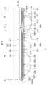
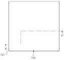
도 1은 본 발명의 일 실시 형태에 따른 반도체 발광소자의 개략적인 평면도이다.
도 2는 도 1의 반도체 발광소자를 A-A'를 따라 절개한 측단면도이다.
도 3은 도 2의 B부분의 확대도이다.
도 4(a) 내지 도 4(d)는 도 1의 솔더 패드의 변형예이다.
도 5a 내지 도 10b는 도 1의 반도체 발광소자의 제조공정을 나타내는 주요 단계별 도면들이다.
도 11a 및 도 11b는 본 발명의 일 실시 형태에 따른 반도체 발광소자를 반도체 발광소자 패키지에 적용한 예를 나타내는 측단면도이다.
도 12 및 도 13은 본 발명의 일 실시 형태에 따른 반도체 발광소자 패키지를 백라이트 유닛에 적용한 예를 나타내는 단면도이다.
도 14 및 도 15는 본 발명의 일 실시 형태에 따른 반도체 발광소자 패키지를 조명장치에 적용한 예를 나타내는 도면이다.1 is a schematic plan view of a semiconductor light emitting device according to an embodiment of the present invention.
2 is a side cross-sectional view of the semiconductor light emitting device of FIG. 1 taken along line A-A'.
3 is an enlarged view of part B of FIG. 2.
4(a) to 4(d) are modified examples of the solder pad of FIG. 1.
5A to 10B are main step-by-step views illustrating a manufacturing process of the semiconductor light emitting device of FIG. 1.
11A and 11B are side cross-sectional views illustrating an example in which a semiconductor light emitting device according to an embodiment of the present invention is applied to a semiconductor light emitting device package.
12 and 13 are cross-sectional views illustrating an example in which a semiconductor light emitting device package according to an embodiment of the present invention is applied to a backlight unit.
14 and 15 are views showing an example in which a semiconductor light emitting device package according to an embodiment of the present invention is applied to a lighting device.
이하, 첨부된 도면을 참조하여 본 발명의 바람직한 실시 형태들을 설명한다. 그러나, 본 발명의 실시형태는 여러 가지 다른 형태로 변형될 수 있으며, 본 발명의 범위가 이하 설명하는 실시 형태로 한정되는 것은 아니다. 또한, 본 발명의 실시형태는 당해 기술분야에서 평균적인 지식을 가진 자에게 본 발명을 더욱 완전하게 설명하기 위해서 제공되는 것이다. 따라서, 도면에서 요소들의 형상 및 크기 등은 보다 명확한 설명을 위해 과장될 수 있으며, 도면 상의 동일한 부호로 표시되는 요소는 동일한 요소이다.
Hereinafter, preferred embodiments of the present invention will be described with reference to the accompanying drawings. However, the embodiments of the present invention may be modified into various other forms, and the scope of the present invention is not limited to the embodiments described below. In addition, embodiments of the present invention are provided in order to more completely explain the present invention to those with average knowledge in the art. Accordingly, shapes and sizes of elements in the drawings may be exaggerated for clearer description, and elements indicated by the same reference numerals in the drawings are the same elements.
본 명세서에서, '상', '상부', '상면', '하', '하부', '하면', '측면' 등의 용어는 도면을 기준으로 한 것이며, 실제로는 소자나 패키지가 배치되는 방향에 따라 달라질 수 있을 것이다. 도 1 내지 도 3을 참조하여, 본 발명의 일 실시형태에 따른 반도체 발광소자 패키지에 대해 설명한다. 도 1은 본 발명의 일 실시 형태에 따른 반도체 발광소자의 개략적인 평면도이고, 도 2는 도 1의 반도체 발광소자를 A-A'를 따라 절개한 측단면도이며, 도 3은 도 2의 B부분의 확대도이다.
In this specification, terms such as'top','top','top','bottom','bottom','bottom', and'side' are based on drawings, and in reality, It may be different depending on the direction. A semiconductor light emitting device package according to an embodiment of the present invention will be described with reference to FIGS. 1 to 3. 1 is a schematic plan view of a semiconductor light emitting device according to an embodiment of the present invention, FIG. 2 is a side cross-sectional view of the semiconductor light emitting device of FIG. 1 taken along line A-A', and FIG. 3 is a part B of FIG. Is an enlarged view of.
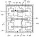
도 1 내지 도 3을 참조하면, 본 발명의 일 실시 형태에 의한 반도체 발광소자(1)는 발광다이오드 칩(10), 패시베이션층(400), 솔더 패드(500) 및 솔더 범프(S)를 포함하여 구성될 수 있다.
1 to 3, a semiconductor
발광다이오드 칩(10)은 발광 구조물(100) 및 제1 및 제2 전극(140, 150)을 포함하여 구성될 수 있으며, 제1 및 제2 전극(140, 150)이 배치된 제1 면과 상기 제1 면의 반대에 위치한 제2 면을 가질 수 있다.The light
발광 구조물(100)은 복수의 반도체층이 적층된 구조를 가지며, 기판(101) 상에 순차적으로 적층된 제1 도전형 반도체층(110), 활성층(120) 및 제2 도전형 반도체층(130)을 포함할 수 있다.
The
기판(101)은 x 방향 및 y 방향으로 연장되는 상면을 가질 수 있다. 기판(101)은 반도체 성장용 기판으로 제공될 수 있으며, 사파이어, Si, SiC, MgAl2O4, MgO, LiAlO2, LiGaO2, GaN 등과 같이 절연성, 도전성, 반도체 물질을 이용할 수 있다. 질화물 반도체 성장용 기판으로 널리 이용되는 사파이어는, 전기 절연성을 가지며 육각-롬보형(Hexa-Rhombo R3c) 대칭성을 갖는 결정체로서 c축 및 a측 방향의 격자상수가 각각 13.001Å과 4.758Å이며, C(0001)면, A(11-20)면, R(1-102)면 등을 갖는다. 이 경우, 상기 C면은 비교적 질화물 박막의 성장이 용이하며, 고온에서 안정하기 때문에 질화물 성장용 기판으로 주로 사용된다.The
그리고, 도면에서 도시하는 것과 같이, 기판(101)의 상면, 즉, 반도체층들이 성장하는 면에는 다수의 요철 구조(102)가 형성될 수 있으며, 이러한 요철 구조(102)에 의하여 반도체층들의 결정성과 광 방출 효율 등이 향상될 수 있다. 본 실시 형태에서는 상기 요철 구조(102)가 돔 형상의 볼록한 형태를 가지는 것으로 예시하고 있으나, 이에 한정하는 것은 아니다. 예를 들어, 상기 요철 구조(102)는 사각형, 삼각형 등의 다양한 형태로 형성될 수 있다. 또한, 상기 요철 구조(102)는 선택적으로 형성 및 구비될 수 있으며, 실시 형태에 따라서 생략될 수도 있다.
And, as shown in the figure, a plurality of
한편, 이러한 기판(101)은 실시 형태에 따라서 추후 제거될 수도 있다. 즉, 제1 도전형 반도체층(110), 활성층(120) 및 제2 도전형 반도체층(130)을 성장시키기 위한 성장용 기판으로 제공된 후 분리 공정을 거쳐 제거될 수 있다. 기판(101)의 분리는 레이저 리프트 오프(Laser Lift Off, LLO), 케미컬 리프트 오프(Chemical Lift Off, CLO) 등의 방식을 통해 반도체층들과 분리될 수 있다.
Meanwhile, the
도면에는 도시되지 않았으나, 기판(101)의 상면에는 버퍼층이 더 구비될 수 있다. 버퍼층은 기판(101) 상에 성장되는 반도체층의 격자 결함 완화를 위한 것으로, 질화물 등으로 이루어진 언도프 반도체층으로 이루어질 수 있다. 버퍼층은, 예를 들어, 사파이어로 이루어진 기판(101)과 기판(101) 상면에 적층되는 GaN으로 이루어진 제1 도전형 반도체층(110) 사이의 격자상수 차이를 완화하여, GaN층의 결정성을 증대시킬 수 있다. 버퍼층은 언도프 GaN, AlN, InGaN 등이 적용될 수 있으며, 500℃ 내지 600℃의 저온에서 수십 내지 수백 Å의 두께로 성장시켜 형성할 수 있다. 여기서, 언도프라 함은 반도체층에 불순물 도핑 공정을 따로 거치지 않은 것을 의미하며, 반도체층에 본래 존재하던 수준의 불순물 농도, 예컨대, 질화갈륨 반도체를 유기 금속 화학 증착(Metal Organic Chemical Vapor Deposition, MOCVD)를 이용하여 성장시킬 경우, 도펀트로 사용되는 Si 등이 의도하지 않더라도 약 1014~ 1018/㎤의 수준으로 포함될 수 있다. 다만, 이러한 버퍼층은 본 실시 형태에서 필수적인 요소는 아니며 실시 형태에 따라 생략될 수도 있다.
Although not shown in the drawing, a buffer layer may be further provided on the upper surface of the
상기 기판(101) 상에 적층되는 제1 도전형 반도체층(110)은 n형 불순물이 도핑된 반도체로 이루어질 수 있으며, n형 질화물 반도체층일 수 있다. 그리고, 제2 도전형 반도체층(130)은 p형 불순물이 도핑된 반도체로 이루어질 수 있으며, p형 질화물 반도체층일 수 있다. 다만, 실시 형태에 따라서 제1 및 제2 도전형 반도체층(110, 130)은 위치가 바뀌어 적층될 수도 있다. 이러한 제1 및 제2 도전형 반도체층(110, 130)은 AlxInyGa(1-x-y)N 조성식(여기서, 0≤x<1, 0≤y<1, 0≤x+y<1임)을 가지며, 예컨대, GaN, AlGaN, InGaN, AlInGaN 등의 물질이 이에 해당될 수 있다.
The first conductivity-
제1 및 제2 도전형 반도체층(110, 130) 사이에 배치되는 활성층(120)은 전자와 정공의 재결합에 의해 소정의 에너지를 갖는 광을 방출한다. 활성층(120)은 제1 및 제2 도전형 반도체층(110, 130)의 에너지 밴드 갭보다 작은 에너지 밴드 갭을 갖는 물질을 포함할 수 있다. 예를 들어, 제1 및 제2 도전형 반도체층(110, 130)이 GaN계 화합물 반도체인 경우, 활성층(120)은 GaN의 에너지 밴드 갭보다 작은 에너지 밴드 갭을 갖는 InGaN계 화합물 반도체를 포함할 수 있다. 또한, 활성층(120)은 양자우물층과 양자장벽층이 서로 교대로 적층된 다중 양자우물(Multiple Quantum Wells, MQW) 구조, 예컨대, InGaN/GaN 구조가 사용될 수 있다. 다만, 이에 제한되는 것은 아니므로 상기 활성층(120)은 단일 양자우물 구조(Single Quantum Well, SQW)가 사용될 수도 있다.
The
상기 발광 구조물(100)은, 상기 제2 도전형 반도체층(130), 상기 활성층(120) 및 상기 제1 도전형 반도체층(110)의 일부가 식각된 식각 영역(E)과, 상기 식각 영역(E)에 의해 부분적으로 구획된 복수의 메사 영역(M)을 포함할 수 있다.The
상기 식각 영역(E)은 상부에서 바라보았을 때 사각 형태를 갖는 상기 발광 구조물(100)의 일측면에서 이와 대향하는 타측면을 향해 소정 두께 및 길이로 절개된 틈새 구조를 가질 수 있다. 그리고, 상기 발광 구조물(100)의 사각 형태의 영역 안쪽에서 복수개가 서로 평행하게 배열되어 구비될 수 있다. 따라서, 상기 복수의 식각 영역(E)은 상기 메사 영역(M)에 의해 둘러싸이는 구조로 구비될 수 있다.
The etched region E may have a gap structure cut from one side of the
상기 식각 영역(E)으로 노출되는 상기 제1 도전형 반도체층(110)의 상부면에는 제1 전극(140)이 배치되어 상기 제1 도전형 반도체층(110)과 접속되고, 상기 복수의 메사 영역(M)의 상부면에는 제2 전극(150)이 배치되어 상기 제2 도전형 반도체층(130)과 접속될 수 있다. 상기 제1 및 제2 전극(140, 150)은 상기 발광 구조물(100)이 위치한 상기 발광다이오드 칩(10)의 제1 면에 배치될 수 있다. 따라서, 상기 제1 및 제2 전극(140, 150)은 발광다이오드 칩(10)의 동일한 면에 배치되어, 상기 발광다이오드 칩(10)이 후술할 패키지 본체(1002)에 플립 칩(flip-chip) 방식으로 실장되도록 할 수 있다.
A
상기 제1 전극(140)은, 도 1에 도시된 것과 같이 복수의 패드부(141) 및 이보다 폭이 좁은 형태로 상기 복수의 패드부(141)로부터 각각 연장되는 복수의 핑거부(142)를 포함하며, 상기 식각 영역(E)을 따라 연장될 수 있다. 그리고, 상기 제1 전극(140)은 복수개가 상기 제1 도전형 반도체층(110) 상에 전체적으로 균일하게 분포될 수 있도록 간격을 두고 배열될 수 있다. 따라서, 상기 복수의 제1 전극(140)을 통해 상기 제1 도전형 반도체층(110)으로 주입되는 전류는 상기 제1 도전형 반도체층(110) 전체에 걸쳐 균일하게 주입될 수 있다.As shown in FIG. 1, the
상기 복수의 패드부(141)는 서로 이격되어 배치될 수 있으며, 상기 복수의 핑거부(142)는 각각 상기 복수의 패드부(141)를 연결할 수 있다. 상기 복수의 핑거부(142)는 서로 상이한 크기의 폭을 가질 수 있다. 예를 들어, 본 실시 형태에서와 같이 제1 전극(140)이 3개의 핑거부(142)를 가지는 경우, 어느 하나의 핑거부(142)의 폭이 상대적으로 다른 핑거부(142)의 폭 보다 클 수 있다. 이러한 어느 하나의 핑거부(142)의 폭은 상기 제1 전극(140)을 통해 주입되는 전류의 저항을 고려하여 폭의 크기를 조절할 수 있다.
The plurality of
상기 제2 전극(150)은 반사 메탈층(151)을 포함할 수 있다. 그리고, 상기 반사 메탈층(151)을 덮는 피복 메탈층(152)을 더 포함할 수 있다. 다만, 이러한 피복 메탈층(152)은 선택적으로 구비될 수 있으며, 실시 형태에 따라서 생략될 수도 있다. 상기 제2 전극(150)은 상기 메사 영역(M)의 상부면을 정의하는 상기 제2 도전형 반도체층(130)의 상면을 덮는 형태로 구비될 수 있다.
The
한편, 상기 식각 영역(E)으로 노출되는 상기 활성층(120)을 덮도록 상기 메사 영역(M)의 측면을 포함하는 발광 구조물(100) 상에는 절연 물질로 이루어지는 제1 절연층(200a)이 구비될 수 있다. 예를 들어, 상기 제1 절연층(200a)은 SiO2, SiN, SiOxNy, TiO2, Si3N4, Al2O3, TiN, AlN, ZrO2, TiAlN, TiSiN 등의 물질을 포함하는 절연성 물질로 이루어질 수 있다. 또한, 상기 제1 절연층(200a)은 상기 제1 및 제2 전극(140, 150)을 노출시키는 형태로 구비될 수 있다. 다만, 상기 제1 절연층(200a)은 선택적으로 구비되는 것으로, 실시 형태에 따라서 생략될 수도 있다.
Meanwhile, a first insulating
제2 절연층(200)은 상기 발광 구조물(100)을 전체적으로 덮는 구조로 상기 발광 구조물(100) 상에 구비될 수 있다. 상기 제2 절연층(200)은 기본적으로 절연 특성을 지닌 재료로 이루어질 수 있으며, 무기질 또는 유기질 물질을 사용하여 형성될 수 있다. 예를 들어, 상기 제2 절연층(200)은 에폭시계 절연 수지로 형성될 수 있다. 또한, 상기 제2 절연층(200)은 실리콘 산화물 또는 실리콘 질화물을 포함하여 이루어질 수 있으며, 예를 들어, SiO2, SiN, SiOxNy, TiO2, Si3N4, Al2O3, TiN, AlN, ZrO2, TiAlN, TiSiN 등으로 이루어질 수 있다.
The second
상기 제2 절연층(200)은 상기 제1 전극(140)과 제2 전극(150) 상에 각각 배치되는 복수의 개구부(210)를 구비할 수 있다. 구체적으로, 상기 복수의 개구부(210)는 각각 상기 제1 전극(140)과 제2 전극(150)과 대응되는 위치에 구비되어 해당 제1 전극(140)과 제2 전극(150)을 부분적으로 노출시킬 수 있다.The second
특히, 상기 복수의 개구부(210) 중 상기 제1 전극(140) 상에 배치되는 개구부(210)는 상기 제1 전극(140)의 패드부(141)만을 외부로 노출시킬 수 있다. 따라서, 상기 복수의 개구부(210)는 상기 제1 전극(140) 상에서는 상기 패드부(141)와 대응하는 위치에 배치될 수 있다.
In particular, the
배리어 메탈층(300)은 상기 제2 절연층(200) 상에 구비되며, 상기 복수의 개구부(210)를 통해 상기 제1 도전형 반도체층(110) 및 상기 제2 도전형 반도체층(130)과 각각 전기적으로 접속될 수 있다.The
도 2에서 도시하는 바와 같이, 상기 배리어 메탈층(300)은 상기 발광 구조물(100)의 상부면을 전체적으로 덮는 상기 제2 절연층(200)에 의해 상기 제1 및 제2 도전형 반도체층(110, 130)과 절연될 수 있다. 그리고, 상기 복수의 개구부(210)를 통해 부분적으로 노출되는 상기 제1 전극(140) 및 제2 전극(150)과 연결되어 상기 제1 및 제2 도전형 반도체층(110, 130)과 전기적으로 접속될 수 있다.As shown in FIG. 2, the
상기 배리어 메탈층(300)과 상기 제1 및 제2 도전형 반도체층(110, 130)의 전기적 연결은 상기 제2 절연층(200)에 구비되는 상기 복수의 개구부(210)에 의해 다양하게 조절될 수 있다. 예를 들어, 상기 복수의 개구부(210)의 개수 및 배치 위치에 따라서 상기 배리어 메탈층(300)과 상기 제1 및 제2 도전형 반도체층(110, 130)과의 전기적 연결은 다양하게 변경될 수 있다.
Electrical connection between the
상기 배리어 메탈층(300)은 제1 메탈층(310) 및 제2 메탈층(320)을 포함하여 적어도 한 쌍으로 구비될 수 있다. 즉, 상기 제1 메탈층(310)은 상기 제1 전극(140)을 통해 상기 제1 도전형 반도체층(110)과 전기적으로 접속하고, 상기 제2 메탈층(320)은 상기 제2 전극(150)을 통해 제2 도전형 반도체층(130)과 전기적으로 접속할 수 있다. 이 경우, 상기 제1 전극(140)을 노출시키는 상기 개구부(210)는 상기 제1 메탈층(310)과 중첩되는 위치에 배치되고, 상기 제2 전극(150)을 노출시키는 상기 개구부(210)는 상기 제2 메탈층(320)과 중첩되는 위치에 배치될 필요가 있다. 그리고, 상기 제1 및 제2 메탈층(310, 320)은 서로 분리되어 전기적으로 절연될 수 있다.The
상기 배리어 메탈층(300)은, 예를 들어, Au, W, Pt, Si, Ir, Ag, Cu, Ni, Ti, Cr 등의 물질 및 그 합금 중 하나 이상을 포함한 물질로 이루어질 수 있다.
The
한편, 상기 제1 전극(140) 중 상기 제2 메탈층(320)이 상부에 위치하여 상기 제2 메탈층(320)과 중첩되는 위치에 배치되는 제1 전극(140)의 경우 상기 제2 메탈층(320)과 전기적으로 접속되는 것을 차단할 필요가 있다. 이를 위해 상기 제2 절연층(200)은 상기 제1 전극(140)의 패드부(141)를 노출시키는 개구부(210)를 상기 제2 메탈층(320)이 상부에 위치하는 부분에 구비하지 않을 수 있다.On the other hand, in the case of the
구체적으로, 도 1에서 도시하는 바와 같이 제1 전극(140)이 4개의 패드부(141)와 3개의 핑거부(142)를 포함하여 이루어지는 경우, 패드부(141)를 노출시키는 개구부(210)는 제1 메탈층(310)과 중첩되는 위치에 배치되는 3개의 패드부(141) 상에만 구비되고 제2 메탈층(320)과 중첩되는 위치에 배치되는 나머지 패드부(141) 상에는 구비되지 않는다. 따라서, 제1 메탈층(310)의 하부에 위치하는 제1 전극(140)의 패드부(141)는 상기 개구부(210)를 통해 상기 제1 메탈층(310)과 접속하지만, 제2 메탈층(320)의 하부에 위치하는 패드부(141) 상에는 상기 개구부(210)가 구비되지 않아 상기 패드부(141)와 제2 메탈층(320)은 서로 전기적으로 절연될 수 있다. 결국, 제1 전극(140)과 제2 전극(150)을 각각 부분적으로 노출시키는 복수의 개구부(210)의 배열 구조를 통해서 제1 메탈층(310)은 제1 전극(140)과 접속하고, 제2 메탈층(320)은 제2 전극(150)과 접속할 수 있다.
Specifically, as shown in FIG. 1, when the
패시베이션층(400)은 상기 배리어 메탈층(300) 상에 구비되며, 상기 배리어 메탈층(300)을 전체적으로 덮어 보호한다. 그리고, 상기 패시베이션층(400)은 상기 배리어 메탈층(300)을 부분적으로 노출시키는 본딩 영역(410)을 구비할 수 있다.The
상기 본딩 영역(410)은 상기 제1 메탈층(310) 및 제2 메탈층(320)을 각각 부분적으로 노출시킬 수 있도록 복수개로 구비될 수 있다. 이 경우, 상기 복수의 본딩 영역(410) 중 일부는 상기 제2 절연층(200)의 복수의 개구부(210) 중 일부와 서로 중첩되지 않는 구조로 배치될 수 있다. 예를 들어, 도 2에서 도시하는 바와 같이, 상기 복수의 본딩 영역(410) 중 상기 제2 메탈층(320)을 부분적으로 노출시키는 본딩 영역(410)은 상기 복수의 개구부(210) 중 상기 제2 전극(150)을 부분적으로 노출시키는 개구부(210)와 서로 중첩되지 않을 수 있다. 즉, 수직 방향으로 상기 개구부(210)의 상부에는 상기 본딩 영역(410)이 위치하지 않는다. 그리고, 상기 제1 메탈층(310)을 부분 노출시키는 본딩 영역(410)은 상기 제1 전극(140)을 부분 노출시키는 개구부(210)와 부분적으로 중첩될 수 있다.The
본 실시 형태에서는 상기 본딩 영역(410)이 4개로 구비되며 대칭 구조를 이루며 배치되는 것으로 예시하고 있으나, 이에 한정하는 것은 아니다. 상기 본딩 영역(410)의 개수 및 배치 형태는 다양하게 변형될 수 있다.In the present embodiment, four
상기 패시베이션층(400)은 상기 제2 절연층(200)과 동일한 재질로 이루어질 수 있다.The
한편, 상기 패시베이션층(400)은 상기 본딩 영역(410)과 마찬가지로 상기 제1 및 제2 메탈층(310, 320)을 부분 노출시키는 오픈 영역(430)을 더 구비할 수 있다. 이러한 오픈 영역(430)은 반도체 발광소자를 장착하기 전에 작동 여부를 확인할 수 있도록 프로브 핀(미도시)과 접속하는 영역으로 제공될 수 있다.
Meanwhile, like the
상기 솔더 패드(500)는 상기 본딩 영역(410)에 각각 배치되되, 각각 분리된 복수의 영역을 가질 수 있다.Each of the
솔더 패드(500)는 제1 솔더 패드(510) 및 제2 솔더 패드(520)를 포함할 수 있으며, 상기 본딩 영역(410)을 통해 부분적으로 노출되는 상기 제1 및 제2 메탈층(310, 320)과 각각 연결될 수 있다. 그리고, 상기 배리어 메탈층(300)을 통해 상기 제1 도전형 반도체층(110) 및 제2 도전형 반도체층(130)과 각각 전기적으로 접속할 수 있다. 이러한 솔더 패드(500)는 Ni, Au, Cu 등의 물질 및 그 합금 중 하나 이상을 포함한 물질로 이루어질 수 있다. 또한, 솔더 패드(500)는 수직에 가까운 측면을 갖도록 형성될 수 있다. 그러나, 반드시 이에 한정하는 것은 아니며, 도 3에 도시된 바와 같이, 솔더 패드(500)의 측면은 소정의 경사각(θ)을 갖도록 형성될 수도 있다.
The
상기 제1 솔더 패드(510) 및 제2 솔더 패드(520)는, 예를 들어, UBM(Under Bump Metallurgy) 층일 수 있다. 그리고, 각각 단일 또는 복수개로 구비될 수 있다. 본 실시 형태에서는 제1 솔더 패드(510)와 제2 솔더 패드(520)가 각각 2개로 구비되는 것으로 예시하고 있으나 이에 한정하는 것은 아니다. 상기 제1 솔더 패드(510)와 제2 솔더 패드(520)의 개수와 배치 구조는 상기 본딩 영역(410)에 따라 조절될 수 있다.
The first and
상기 제1 및 제 2 솔더 패드(510, 520)에는 솔더 범프(S)가 각각 배치될 수 있다. 이러한 솔더 범프(S)는 상기 발광다이오드 칩(10)을 패키지 기판에 플립 칩(flip-chip) 방식으로 실장하기 위한 도전성 접착물로서 Sn 솔더가 사용될 수 있으며, 이러한 Sn 솔더에는 Ag 및 Cu와 같은 물질이 미량 함유될 수 있다.
Solder bumps S may be disposed on the first and
이와 같이, 솔더 패드(500)에는 솔더 범프(S)가 배치되어, 후속 공정에서 패키지 기판에 발광다이오드 칩(10)을 실장하는데 사용될 수 있다.As described above, the solder bump S is disposed on the
그러나, 솔더 패드(500)에 솔더 범프(S)를 배치하면, 도 3에 도시된 바와 같이, 솔더 패드(500)와 솔더 범프(S)의 물질이 서로 반응하여, 솔더 패드(500)에 솔더 범프(S)가 접하는 면에 금속간 화합물층(inter-metallic compound layer)(501a)이 형성될 수 있다. 예를 들어, 금속간 화합물층은 Sn-Ni 합금일 수 있다.However, when the solder bump (S) is disposed on the solder pad (500), as shown in FIG. 3, the material of the solder pad (500) and the solder bump (S) react with each other, thereby soldering the solder pad (500). An
이러한 금속간 화합물층(501a)은 일반적으로 솔더 범프(S)를 이루는 물질에 비해 탄성계수가 작고 취성(brittleness)이 큰 특성을 가진다. 따라서, 솔더 패드(500) 상에 솔더 범프(S)가 배치된 후, 후속 공정에서 외부의 충격이 가해질 경우, 금속간 화합물층(501a)에 균열(F)이 쉽게 발생하는 문제가 발생할 수 있다. 이러한 균열(F)은 금속물 화합물층(501a)의 일 영역에서 시작되나, 금속간 화합물층(501a)을 따라 금속간 화합물층(501a)의 전 영역으로 전파되게 된다. 이와 같이, 균열(F)이 금속간 화합물층(501a)의 전 영역으로 전파되면 솔더 범프(S)가 솔더 패드(500)에서 완전히 분리되는, 이른바 오픈(open) 불량을 야기할 수 있다.In general, the
특히, 금속간 화합물층(501a)의 측면은 충격이 직접적으로 전달될 수 있으므로, 균열(F)이 발생되기 쉽다.
In particular, the side surface of the
본원발명은 금속간 화합물층(501a)의 일 영역에서 발생한 균열(F)이 금속간 화합물층(501a)의 전 영역으로 전파되는 것을 방지하기 위해, 솔더 범프(S)와 접하는 각각의 솔더 패드(500)를 분리된 복수의 영역(511, 512, 522, 521)으로 분할하여 배치하였다. 이와 같이, 솔더 패드(500)를 복수의 영역으로 분할하면 금속간 화합물층(501a)의 일 영역에서 발생된 균열이, 금속간 화합물층(501a)의 전 영역으로 전파되는 것을 효과적으로 방지할 수 있다. 따라서, 솔더 범프(S)가 솔더 패드(500)에서 완전히 분리되는 오픈(open) 불량을 미연에 방지할 수는 효과가 있다.
In the present invention, each
이를 구체적으로 설명하면, 상기 솔더 패드(500)는 각각 분리된 복수의 영역(511, 512, 522, 521)을 갖도록 배치될 수 있다. 예를 들어, 도 1에 도시된 바와 같이, 제1 솔더 패드(510)는 하나의 중심부(511)와 중심부(511)를 둘러싸는 복수개의 주변부(512)로 구성될 수 있으며, 제2 솔더 패드(520)도 동일하게, 중심부(521)과 중심부(521)를 둘러싸는 복수개의 주변부(522)로 구성될 수 있다. 이러한 중심부(511)는 소정의 폭(W2)을 가지며, 주변부(512)와 소정의 이격된 영역(W1)을 갖도록 이격 배치될 수 있다. 이격된 영역(W1)은 반드시 균일한 폭을 가지도록 배치되어야 하는 것은 아니나, 적어도 솔더 패드(500)의 분리된 영역에 형성된 금속간 화합물층(501a, 501b)이 서로 맞닿지 않을 정도의 간격을 가지도록 형성되는 것으로 배치될 수 있다. 다만, 솔더 패드(500)의 분리된 영역은 완전히 격리된 영역으로 분리되어야 하는 것은 아니며, 솔더 패드(500)의 둘레로부터 만입된 영역을 갖도록 배치될 수도 있다.
Specifically, the
이격된 영역(W1)은 중심부(511) 또는 주변부(512)의 폭(W2)보다 좁게 형성될 수 있다. 이격된 영역(W1)의 면적은 솔더 패드(510, 520)가 차지하는 면적의 70% 이하의 면적을 갖도록 구성될 수 있다.
The spaced apart regions W1 may be formed to be narrower than the width W2 of the
도 3에 도시된 바와 같이, 이러한 이격된 영역(W1)에는 균열(F)의 전파를 더욱 효과적으로 차단할 수 있도록 균열차단층(200b)이 더 배치될 수 있다. 균열차단층(200b)은 SiO2, SiN, SiOxNy, TiO2, Si3N4, Al2O3, TiN, AlN, ZrO2, TiAlN, TiSiN 등의 물질을 포함하는 절연성 물질로 이루어질 수 있으며, 패시베이션층(400)과 동일한 조성이 물질로 이루어질 수도 있다. 이러한 균열차단층(200b)은 균열(F)이 전파되는 것을 더욱 효과적으로 차단할 수 있는데, 이와 관련된 자세한 사항은 후술한다.
As shown in FIG. 3, a
솔더 패드(500)는 다양한 형상으로 변형될 수 있다. 도 4(a) 내지 도 4(d)는 도 1의 솔더 패드의 변형예이다. 도 4(a)는 앞서 설명한 중심부도 복수개의 영역(511a)으로 형성한 경우이다. 도 4(b)는 솔더 패드의 중심부(511b)와 주변부(512b)가 일 영역에서 연결된 경우이다. 따라서, 이격된 영역(W1)은 솔더 패드(510a)의 둘레로부터 만입된 영역(513a)를 갖도록 형성될 수 있다. 도 4(c)는 주변부(512c)가 중심부(511c)를 둘러싸는 형상을 갖도록 형성된 경우이다. 이 경우, 이격된 영역(513c)은 하나의 띠 형상을 갖도록 형성될 수 있다. 4(d)는 이격된 영역(513d)이 솔더 패드(510d) 내에 개구 형상으로 형성된 경우이다.
The
이와 같이, 솔더 패드(500)를 복수의 분리된 영역으로 배치하면, 금속간 화합물층(501a)의 일 영역에서 균열이 발생하더라도, 솔더 패드(500) 중 하나의 분리된 영역에만 균열이 전파될 뿐, 솔더 패드(500) 전체로 전파되지 않는 효과가 있다.In this way, when the
도 3을 참조하여 이를 구체적으로 설명한다. 금속간 화합물층(501a)의 일 영역에서 발생한 균열(F)은 금속간 화합물층(501a)을 따라 전파될 수 있다. 특히, 상기 균열(F)은 충격에 취약한 금속간 화합물층(501a)의 측면에서 발생하기 쉽다. 이와 같이 전파되는 균열(F)은 세 방향(G1, G2, G3)의 진로로 전파되는 것으로 예상할 수 있다. 그러나, 솔더 범프(S)는 금속간 화합물층(501a)보다 탄성계수가 크고 취성(brittleness)이 작은 특성을 가지므로, 균열(F)은 부서지기 쉬운 금속간 화합물층(501a) 방향(G1)으로 진행되게 된다. 따라서, 균열(F)은 솔더 범프(S)를 경유하는 방향(G2) 또는 솔더 범프(S)의 표면을 따라 전파되는 방향(G2)으로 전파되지 못하고, 금속간 화합물층(501a)의 표면을 따라 진행하는 방향(G1)으로만 전파되게 된다. 또한, 솔더 패드(500)가 배치되지 않은 W3영역에는 금속간 화합물층(501a)이 형성되지 못하므로 G1 방향으로 전파된 균열(F)은 더 이상 진행되지 못하게 된다. 따라서, 하나의 금속간 화합물층(501a)에서 발생된 균열(F)이 이웃하는 금속간 화합물층(501b)에 전파되는 것이 효과적으로 차단될 수 있다.
This will be described in detail with reference to FIG. 3. The crack F generated in one region of the
솔더 패드가 분리되지 않은 경우(Ref)와 본 실시 형태의 접착강도를 DST( Die Shear Test)를 통해 비교해 본 결과, Ref의 경우 2.85㎏을 가했을 때에 솔더 범프가 완전히 분리된 반면, 본 실시형태의 경우 3.11㎏을 가했을 때에 솔더 범프가 분리되는 것을 측정되었다. 이로써, 본 실시 형태의 분리된 영역을 갖는 솔더 패드 구조가 Ref와 비교하여, 약 9%의 접착강도가 향상된 것을 확인할 수 있었다.
When the solder pad was not separated (Ref) and the adhesive strength of this embodiment was compared through DST (Die Shear Test), in the case of Ref, when 2.85 kg was added, the solder bump was completely separated. It was measured that the solder bump was separated when 3.11 kg was added. As a result, it was confirmed that the solder pad structure having the separated regions of the present embodiment improved the adhesive strength of about 9% compared to the Ref.
또한, 균열차단층(200b)이 솔더 패드(500)의 분리된 영역(W1)에 더 배치된 경우에는, 일 영역의 금속간 화합물층(501a)과 이웃하는 금속간 화합물층(501a)이 더욱 확실하게 단절되므로 균열(F)이 전파되는 것을 더욱 효과적으로 방지할 수 있다.
In addition, when the
다음으로, 도 1의 반도체 발광소자의 제조공정에 대해 설명한다. 도 5a 내지 도 10b는 도 1의 반도체 발광소자의 제조공정을 나타내는 주요 단계별 도면들이다. 도 5a 내지 도 10b에서, 도 1 내지 도 4와 동일한 참조 부호는 동일한 부재를 나타내며, 따라서 중복되는 설명은 생략한다.Next, the manufacturing process of the semiconductor light emitting device of FIG. 1 will be described. 5A to 10B are main step-by-step views illustrating a manufacturing process of the semiconductor light emitting device of FIG. 1. In FIGS. 5A to 10B, the same reference numerals as in FIGS. 1 to 4 denote the same members, and therefore, overlapping descriptions are omitted.
도 5a 및 도 5b를 참조하면, 도 5a는 기판(101) 상에 형성된 발광 구조물(100)의 평면도를 도시하며, 도 5b는 도 5a의 절단선 A-A'에 대응하는 단면도가 도시된다. 이하의 도 6a 내지 도 10b도 동일한 방식으로 도시된다.
5A and 5B, FIG. 5A is a plan view of a
먼저 기판(101) 상에 요철 구조(102)를 형성할 수 있다. 다만, 실시 형태에 따라 요철 구조(102)는 생략될 수 있다. 기판(101)은, 앞서 설명한 바와 같이, 사파이어, Si, SiC, MgAl2O4, MgO, LiAlO2, LiGaO2, GaN 등의 물질로 이루어진 기판을 사용할 수 있다.First, the
다음으로, 유기 금속 화학 증착(Metal Organic Chemical Vapor Deposition, MOCVD), 수소화 기상 에피택시(Hydride Vapor Phase Epitaxy, HVPE), 분자선 에피택시(Molecular Beam Epitaxy, MBE) 등과 같은 공정을 이용하여, 기판(101) 상에 순차적으로 제1 도전형 반도체층(110), 활성층(120) 및 제2 도전형 반도체층(130)을 성장시켜 복수의 반도체층의 적층구조를 갖는 발광 구조물(100)을 형성한다. 여기서, 제1 도전형 반도체층(110)과 제2 도전형 반도체층(130)은 각각 n형 반도체층 및 p형 반도체층일 수 있다. 발광 구조물(100)에서 제1 도전형 반도체층(110)과 제2 도전형 반도체층(130)의 위치는 서로 바뀔 수 있으며, 제2 도전형 반도체층(130)이 기판(101) 상에 먼저 형성될 수 있다.
Next, using a process such as Metal Organic Chemical Vapor Deposition (MOCVD), Hydro Vapor Phase Epitaxy (HVPE), Molecular Beam Epitaxy (MBE), etc., the substrate 101 ) On the first conductivity
도 6a 및 도 6b를 참조하면, 제1 도전형 반도체층(110)의 적어도 일부가 노출되도록 제2 도전형 반도체층(130), 활성층(120) 및 제1 도전형 반도체층(110)의 일부를 식각할 수 있다. 이에 의해 식각 영역(E)과 상기 식각 영역(E)에 의해 부분적으로 구획된 복수의 메사 영역(M)을 형성할 수 있다.6A and 6B, a second conductivity
식각 공정은 제1 도전형 반도체층(110)이 노출되는 영역을 제외한 영역에 마스크층을 형성한 후, 습식 또는 건식을 통해 메사 영역(M)을 형성할 수 있다. 실시 형태에 따라, 제1 도전형 반도체층(110)은 식각되지 않고 상면만 일부 노출되도록 식각 공정이 수행될 수도 있다.
In the etching process, after forming a mask layer in a region other than the region where the first conductivity
식각 공정에 의해 식각 영역(E)으로 노출되는 메사 영역(M)의 측면에는 제1 절연층(200a)이 형성될 수 있다. 상기 제1 절연층(200a)은 상기 메사 영역(M)의 상면 가장자리와 상기 식각 영역(E)의 바닥면을 일부 포함하여 상기 메사 영역(M)의 측면을 덮는 구조로 형성될 수 있다. 따라서, 상기 식각 영역(E)으로 노출되는 상기 활성층(120)은 상기 절연층(200a)에 의해 외부로 노출되지 않도록 커버될 있다. 다만, 이러한 절연층(200a)은 선택적으로 형성되는 것으로 실시 형태에 따라서 생략될 수도 있다.
A first insulating
도 7a 및 도 7b를 참조하면, 상기 식각 영역(E)과 상기 메사 영역(M) 상에 각각 제1 전극(140)과 제2 전극(150)이 형성될 수 있다. 상기 제1 전극(140)은 상기 식각 영역(E)을 따라서 연장되며, 상기 식각 영역(E)의 바닥면을 정의하는 제1 도전형 반도체층(110)과 접속할 수 있다. 그리고, 상기 제2 전극(150)은 상기 제2 도전형 반도체층(130)과 접속할 수 있다.7A and 7B, a
상기 제1 전극(140)은 복수의 패드부(141) 및 상기 패드부(141)로부터 연장되는 복수의 핑거부(142)를 포함하여 구성될 수 있다. 상기 제2 전극(150)은 반사 메탈층(151)을 포함할 수 있다. 그리고, 상기 반사 메탈층(151)을 덮는 피복 메탈층(152)을 더 포함할 수 있다. 이와 같이, 제1 전극(140)과 제2 전극(150)을 형성하면 발광다이오드 칩(10)이 준비된다.
The
도 8a 및 도 8b를 참조하면, 제2 절연층(200)이 상기 발광다이오드 칩(10)의 표면을 덮는 구조로 구비될 수 있다. 예를 들어, 상기 제2 절연층(200)은 에폭시계 절연 수지로 형성될 수 있다. 또한, 상기 제2 절연층(200)은 실리콘 산화물 또는 실리콘 질화물을 포함하여 이루어질 수 있으며, 예를 들어, SiO2, SiN, SiOxNy, TiO2, Si3N4, Al2O3, TiN, AlN, ZrO2, TiAlN, TiSiN 등으로 이루어질 수 있다.8A and 8B, a second insulating
그리고, 복수의 개구부(210)를 통해 상기 제1 및 제2 도전형 반도체층(110, 130) 상에서 상기 제1 전극(140)과 제2 전극(150)을 부분적으로 노출시킬 수 있다.
In addition, the
도 9a 및 도 9b를 참조하면, 배리어 메탈층(300)이 상기 제2 절연층(200) 상에 형성될 수 있다. 그리고, 개구부(210)를 통해 상기 노출된 상기 제1 및 제2 전극(140, 150)과 연결되어 상기 제1 도전형 반도체층(110) 및 상기 제2 도전형 반도체층(130)과 각각 전기적으로 접속될 수 있다.9A and 9B, a
상기 배리어 메탈층(300)은 상기 제1 도전형 반도체층(110) 및 제2 도전형 반도체층(130) 사이의 전기적 절연을 위해 적어도 한 쌍으로 구비될 수 있다. 즉, 제1 메탈층(310)은 상기 제1 전극(140)을 통해 상기 제1 도전형 반도체층(110)과 전기적으로 접속하고, 제2 메탈층(320)은 상기 제2 전극(150)을 통해 상기 제2 도전형 반도체층(130)과 전기적으로 접속하며, 상기 제1 및 제2 메탈층(310, 320)은 서로 분리되어 전기적으로 절연될 수 있다.
The
도 10a 및 도 10b를 참조하면, 패시베이션층(400)이 상기 배리어 메탈층(300) 상에 형성될 수 있다. 그리고, 상기 패시베이션층(400)은 본딩 영역(410)을 통해 상기 배리어 메탈층(300)을 부분적으로 노출시킬 수 있다.10A and 10B, a
상기 본딩 영역(410)은 상기 제1 메탈층(310) 및 제2 메탈층(320)을 각각 부분적으로 노출시킬 수 있도록 복수개로 구비될 수 있다. 이 경우, 상기 복수의 본딩 영역(410) 중 일부는 상기 제2 절연층(200)의 복수의 개구부(210) 중 일부와 서로 중첩되지 않는 구조로 배치될 수 있다. 예를 들어, 도 10a에서 도시하는 바와 같이, 상기 복수의 본딩 영역(410) 중 상기 제2 메탈층(320)을 부분적으로 노출시키는 본딩 영역(410)은 상기 복수의 개구부(210) 중 상기 제2 전극(150)을 부분적으로 노출시키는 개구부(210)와 서로 중첩되지 않을 수 있다. 즉, 수직 방향으로 상기 개구부(210)의 상부에는 상기 본딩 영역(410)이 위치하지 않는다.The
상기 패시베이션층(400)은 상기 제2 절연층(200)과 동일한 재질로 이루어질 수 있다.
The
한편, 상기 본딩 영역(410)을 통해 부분적으로 노출되는 상기 제1 및 제2 메탈층(310, 320) 상에 각각 제1 솔더 패드(510) 및 제2 솔더 패드(520)를 포함하는 솔더 패드(500)가 형성될 수 있다. 상기 제1 솔더 패드(510) 및 제2 솔더 패드(520)는, 예를 들어, UBM(Under Bump Metallurgy) 층일 수 있다. 상기 제1 솔더 패드(510)과 제2 솔더 패드(520)의 개수와 배치 구조는 도면에 한정하지 않고 앞서 설명한 바와 같이, 다양하게 변경될 수 있다.Meanwhile, a solder pad including a
또한, 도 10a에서와 같이, 상기 패시베이션층(400)은 상기 본딩 영역(410)과 마찬가지로 상기 제1 및 제2 메탈층(310, 320)을 각각 부분적으로 노출시키는 오픈 영역(430)을 더 구비할 수 있다. 이러한 오픈 영역(430)은 제조된 반도체 발광소자가 제품으로 출하되기 전에 동작 여부를 확인할 수 있도록 하기 위한 것으로 프로브 핀(미도시)을 상기 오픈 영역(430)으로 노출된 제1 및 제2 메탈층(310, 320)과 접속시켜 구동 전원을 공급함으로써 반도체 발광소자의 동작을 확인할 수 있다.In addition, as shown in FIG. 10A, the
이때, 본딩 영역(410) 중 후속공정에서 솔더 패드(500)가 배치되지 않는 영역, 즉 이격된 영역이 될 영역에는 균열차단층(200b)이 더 형성될 수 있다. 상기 균열차단층(200b)은 상기 패시베이션층(400)과 동일한 재질로 이루어질 수 있으며, 상기 패시베이션층(400)과 동시에 형성할 수도 있다.
In this case, a
도 11a 및 도 11b는 각각 본 발명의 일 실시 형태에 따른 반도체 발광소자를 반도체 발광소자 패키지에 적용한 예를 개략적으로 나타내는 단면도이다.11A and 11B are cross-sectional views schematically illustrating an example in which a semiconductor light emitting device according to an embodiment of the present invention is applied to a semiconductor light emitting device package, respectively.
도 11a를 참조하면, 반도체 발광소자 패키지(1000)는 광원인 반도체 발광소자(1001), 패키지 본체(1002), 한 쌍의 리드 프레임(1010) 및 봉지부(1005)를 포함할 수 있다. 여기서 반도체 발광소자(1001)는 상기 도 1의 반도체 발광소자(1)일 수 있으며, 이에 대한 설명은 생략한다.
Referring to FIG. 11A, the semiconductor light emitting
상기 반도체 발광소자(1001)는 상기 리드 프레임(1010)에 실장되고, 도전성 접착 물질을 통해 상기 리드 프레임(1010)과 전기적으로 연결될 수 있다. 도전성 접착 물질로는, 예를 들어, Sn을 포함하는 솔더 범프(S)가 사용될 수 있다.The semiconductor
한 쌍의 리드 프레임(1010)은 제1 리드 프레임(1012)과 제2 리드 프레임(1014)을 포함할 수 있다. 상기 도 1을 참조하면, 반도체 발광소자(1001)의 제1 솔더 패드(510) 및 제2 솔더 패드(520)는 상기 한 쌍의 리드 프레임(1010)과의 사이에 개재되는 솔더 범프(S)를 통해 상기 제1 리드 프레임(1012) 및 제2 리드 프레임(1014)과 각각 연결될 수 있다.The pair of
패키지 본체(1002)에는 빛의 반사 효율 및 광 추출 효율이 향상되도록 반사컵을 구비할 수 있으며, 이러한 반사컵에는 반도체 발광소자(1001)를 봉지하도록 투광성 물질로 이루어진 봉지부(1005)가 형성될 수 있다.
The
도 11b를 참조하면, 반도체 발광소자 패키지(2000)는 반도체 발광소자(2001), 실장 기판(2010) 및 봉지부(2005)를 포함할 수 있다. 여기서 반도체 발광소자(2001)는 상기 도 1의 반도체 발광소자(1)일 수 있으며, 이에 대한 설명은 생략한다.
Referring to FIG. 11B, the semiconductor light emitting
반도체 발광소자(2001)는 실장 기판(2010)에 실장되어 제1 및 제2 회로 패턴(2012, 2014)과 각각 전기적으로 연결될 수 있다. 그리고, 봉지부(2005)에 의해 봉지될 수 있다. 이를 통해 칩 온 보드(Chip On Board, COB) 타입의 패키지 구조를 구현할 수 있다.The semiconductor
실장 기판(2010)은 PCB, MCPCB, MPCB, FPCB 등의 기판으로 제공될 수 있으며, 실장 기판(2010)의 구조는 다양한 형태로 응용될 수 있다.
The mounting
도 12 및 도 13은 본 발명의 일 실시 형태에 따른 반도체 발광소자를 백라이트 유닛에 적용한 예를 나타내는 단면도이다.12 and 13 are cross-sectional views illustrating an example in which a semiconductor light emitting device according to an embodiment of the present invention is applied to a backlight unit.
도 12를 참조하면, 백라이트 유닛(3000)은 기판(3002) 상에 광원(3001)이 실장되며, 그 상부에 배치된 하나 이상의 광학 시트(3003)를 구비한다. 광원(3001)은 도 11a 및 도 11b를 참조하여 상술한 구조 또는 이와 유사한 구조를 갖는 반도체 발광소자 패키지를 이용할 수 있으며, 또한, 반도체 발광소자를 직접 기판(3002)에 실장(소위 COB 타입)하여 이용할 수도 있다.Referring to FIG. 12, the
도 12의 백라이트 유닛(3000)에서 광원(3001)은 액정표시장치가 배치된 상부를 향하여 빛을 방사하는 것과 달리, 도 13에 도시된 다른 예의 백라이트 유닛(4000)은 기판(4002) 위에 실장된 광원(4001)이 측 방향으로 빛을 방사하며, 이렇게 방시된 빛은 도광판(4003)에 입사되어 면광원의 형태로 전환될 수 있다. 도광판(4003)을 거친 빛은 상부로 방출되며, 광 추출 효율을 향상시키기 위하여 도광판(4003)의 하면에는 반사층(4004)이 배치될 수 있다.
Unlike the
도 14 및 도 15는 본 발명의 일 실시 형태에 의한 반도체 발광소자를 조명 장치에 적용한 예를 나타내는 분해사시도이다.14 and 15 are exploded perspective views showing an example in which a semiconductor light emitting device according to an embodiment of the present invention is applied to a lighting device.
도 14를 참조하면, 조명장치(5000)는 벌브형 램프이며, 발광모듈(5003)과 구동부(5008)와 외부접속부(5010)를 포함한다. 또한, 외부 및 내부 하우징(5006, 5009)과 커버부(5007)와 같은 외형구조물을 추가적으로 포함할 수 있다.Referring to FIG. 14, the
발광모듈(5003)은 도 1의 반도체 발광소자(1)와 동일하거나 유사한 구조를 가지는 반도체 발광소자(5001)와 그 반도체 발광소자(5001)가 탑재된 회로기판(5002)을 포함할 수 있다. 본 실시 형태에서는, 한 개의 반도체 발광소자(5001)가 회로기판(5002) 상에 실장된 형태로 예시되어 있으나, 필요에 따라 복수 개로 장착될 수 있다. 또한, 반도체 발광소자(5001)가 직접 회로기판(5002)에 실장되지 않고, 패키지 형태로 제조된 후에 실장될 수도 있다.The
외부 하우징(5006)은 열방출부로 작용할 수 있으며, 발광모듈(5003)과 직접 접촉되어 방열효과를 향상시키는 열방출판(5004) 및 외부 하우징(5006)의 측면을 둘러싸는 방열핀(5005)을 포함할 수 있다. 커버부(5007)는 발광모듈(5003) 상에 장착되며 볼록한 렌즈형상을 가질 수 있다. 구동부(5008)는 내부 하우징(5009)에 장착되어 소켓구조와 같은 외부접속부(5010)에 연결되어 외부 전원으로부터 전원을 제공받을 수 있다. 또한, 구동부(5008)는 발광모듈(5003)의 반도체 발광소자(5001)를 구동시킬 수 있는 적정한 전류원으로 변환시켜 제공하는 역할을 한다. 예를 들어, 이러한 구동부(5008)는 AC-DC 컨버터 또는 정류회로부품 등으로 구성될 수 있다.The
또한, 도면에는 도시되지 않았으나, 조명장치(5000)는 통신 모듈을 더 포함 할 수도 있다.
In addition, although not shown in the drawings, the
도 15를 참조하면, 조명장치(6000)는 일 예로서 바(bar)-타입 램프이며, 발광모듈(6010), 몸체부(6020), 커버부(6030) 및 단자부(6040)를 포함할 수 있다.Referring to FIG. 15, the
발광모듈(6010)은 기판(6012)과, 기판(6012) 상에 장착되는 복수의 반도체 발광소자(6011)을 포함할 수 있다. 반도체 발광소자(6011)는 도 1의 반도체 발광소자(1) 또는 도 11a 및 도 11b의 반도체 발광소자 패키지(1000, 2000)가 채용될 수 있다.The
몸체부(6020)는 리세스(6021)에 의해 발광모듈(6010)을 일면에 장착하여 고정시킬 수 있으며, 발광모듈(6010)에서 발생되는 열을 외부로 방출시킬 수 있다. 따라서, 몸체부(6020)는 지지 구조물의 일종으로 히트 싱크를 포함할 수 있으며, 양 측면에는 방열을 위한 복수의 방열 핀(6022)이 돌출되어 형성될 수 있다.The
커버부(6030)는 몸체부(6020)의 걸림 홈(6023)에 체결되며, 광이 외부로 전체적으로 균일하게 조사될 수 있도록 반원 형태의 곡면을 가질 수 있다. 커버부(6030)의 바닥면에는 몸체부(6020)의 걸림 홈(6023)에 맞물리는 돌기(6031)가 길이 방향을 따라서 형성될 수 있다.The
단자부(6040)는 몸체부(6020)의 길이 방향의 양 끝단부 중 개방된 적어도 일측에 구비되어 발광모듈(6010)에 전원을 공급할 수 있으며, 외부로 돌출된 전극 핀(6041)을 포함할 수 있다.
The
본 발명은 상술한 실시형태 및 첨부된 도면에 의해 한정되는 것이 아니며 첨부된 청구범위에 의해 한정하고자 한다. 따라서, 청구범위에 기재된 본 발명의 기술적 사상을 벗어나지 않는 범위 내에서 당 기술분야의 통상의 지식을 가진 자에 의해 다양한 형태의 치환, 변형 및 변경이 가능할 것이며, 이 또한 본 발명의 범위에 속한다고 할 것이다.
The present invention is not limited by the above-described embodiments and the accompanying drawings, but is intended to be limited by the appended claims. Therefore, various types of substitutions, modifications and changes will be possible by those of ordinary skill in the art within the scope not departing from the technical spirit of the present invention described in the claims, and this also belongs to the scope of the present invention. something to do.
1: 반도체 발광소자
10: 발광다이오드 칩
100: 발광구조물
200a: 제1 절연층
200: 제2 절연층
300: 베리어 메탈층
400: 패시베이션층
500: 솔더 패드
S: 솔더 범프1: semiconductor light emitting device
10: light-emitting diode chip
100: light emitting structure
200a: first insulating layer
200: second insulating layer
300: barrier metal layer
400: passivation layer
500: solder pad
S: Solder bump
Claims (10)
Translated fromKorean상기 제1 및 제2 전극의 본딩 영역들이 노출되도록 상기 발광다이오드 칩의 표면에 배치된 패시베이션층;
상기 본딩 영역들에 각각 배치되며 각각 분리된 복수의 영역을 갖는 복수의 솔더 패드; 및
상기 본딩 영역들에 각각 배치되며, 각각 상기 솔더 패드의 상기 분리된 복수의 영역을 덮는 복수의 솔더 범프를 포함하며,
상기 분리된 복수의 영역은 소정 간격으로 이격된 영역에 의해 분리되고, 상기 이격된 영역에는 균열차단층이 배치된 것을 특징으로 하는 반도체 발광소자.
A light emitting diode chip having a first surface on which first and second electrodes are disposed and a second surface opposite to the first surface;
A passivation layer disposed on the surface of the LED chip to expose bonding regions of the first and second electrodes;
A plurality of solder pads disposed on the bonding areas and each having a plurality of separated areas; And
A plurality of solder bumps disposed on the bonding regions, each covering the plurality of separated regions of the solder pad,
The plurality of separated regions are separated by regions spaced at predetermined intervals, and a crack blocking layer is disposed in the spaced regions.
상기 이격된 영역은 상기 솔더 패드의 상기 분리된 복수의 영역 중 하나를 둘러싸도록 형성된 띠 형상을 갖는 것을 특징으로 하는 반도체 발광소자.
The method of claim 1,
The spaced apart regions have a strip shape formed to surround one of the separated plurality of regions of the solder pad.
상기 균열차단층은 상기 패시베이션층과 동일한 조성의 물질로 형성된 것을 특징으로 하는 반도체 발광소자.
The method of claim 1,
The crack blocking layer is a semiconductor light emitting device, characterized in that formed of a material having the same composition as the passivation layer.
상기 솔더 패드와 상기 솔더 범프가 접하는 면에는 금속간 화합물층(inter-metallic compound layer)이 형성된 것을 특징으로 하는 반도체 발광소자.
The method of claim 1,
A semiconductor light emitting device, wherein an inter-metallic compound layer is formed on a surface of the solder pad and the solder bump contacting each other.
상기 금속간 화합물층은 상기 솔더 패드의 상기 분리된 복수의 영역에 대응하여 분리된 것을 특징으로 하는 반도체 발광소자.
The method of claim 6,
The semiconductor light emitting device, wherein the intermetallic compound layer is separated to correspond to the separated plurality of regions of the solder pad.
상기 금속간 화합물층은 Sn-Ni 합금으로 형성된 것을 특징으로 하는 반도체 발광소자.
The method of claim 7,
The intermetallic compound layer is a semiconductor light emitting device, characterized in that formed of a Sn-Ni alloy.
상기 패키지 본체의 제1 및 제2 리드 프레임 사이에 개재되는 솔더 범프를 통해 상기 리드 프레임과 접속하는 반도체 발광소자를 포함하며,
상기 반도체 발광소자는,
제1 도전형 반도체층, 활성층, 제2 도전형 반도체층을 구비하는 발광 구조물;
제1 및 제2 도전형 반도체층과 각각 전기적으로 접속되며 본딩 영역을 갖는 솔더 패드를 포함하고,
상기 솔더 패드는 둘레로부터 만입된 영역을 가지며,
상기 솔더 범프는 상기 솔더 패드를 덮도록 상기 본딩 영역에 배치되고,
상기 만입된 영역에는 균열차단층이 배치된 것을 특징으로 하는 반도체 발광소자 패키지.
A package body having first and second lead frames; And
A semiconductor light emitting device connected to the lead frame through a solder bump interposed between the first and second lead frames of the package body,
The semiconductor light emitting device,
A light emitting structure including a first conductivity type semiconductor layer, an active layer, and a second conductivity type semiconductor layer;
First and second conductive type semiconductor layers and each electrically connected to each comprising a solder pad having a bonding region,
The solder pad has a depressed area from the periphery,
The solder bump is disposed in the bonding area to cover the solder pad,
A semiconductor light emitting device package, characterized in that a crack blocking layer is disposed in the indented region.
Priority Applications (2)
| Application Number | Priority Date | Filing Date | Title |
|---|---|---|---|
| KR1020140108440AKR102212559B1 (en) | 2014-08-20 | 2014-08-20 | Semiconductor light emitting diode and semiconductor light emitting diode package using the same |
| US14/693,749US9406635B2 (en) | 2014-08-20 | 2015-04-22 | Semiconductor light emitting device and semiconductor light emitting device package using the same |
Applications Claiming Priority (1)
| Application Number | Priority Date | Filing Date | Title |
|---|---|---|---|
| KR1020140108440AKR102212559B1 (en) | 2014-08-20 | 2014-08-20 | Semiconductor light emitting diode and semiconductor light emitting diode package using the same |
Publications (2)
| Publication Number | Publication Date |
|---|---|
| KR20160023010A KR20160023010A (en) | 2016-03-03 |
| KR102212559B1true KR102212559B1 (en) | 2021-02-08 |
Family
ID=55348917
Family Applications (1)
| Application Number | Title | Priority Date | Filing Date |
|---|---|---|---|
| KR1020140108440AActiveKR102212559B1 (en) | 2014-08-20 | 2014-08-20 | Semiconductor light emitting diode and semiconductor light emitting diode package using the same |
Country Status (2)
| Country | Link |
|---|---|
| US (1) | US9406635B2 (en) |
| KR (1) | KR102212559B1 (en) |
Families Citing this family (6)
| Publication number | Priority date | Publication date | Assignee | Title |
|---|---|---|---|---|
| CN104730782B (en)* | 2015-04-01 | 2018-03-27 | 上海天马微电子有限公司 | Array substrate, display panel and display device |
| US10147745B2 (en) | 2015-04-01 | 2018-12-04 | Shanghai Tianma Micro-electronics Co., Ltd. | Array substrate, display panel and display device |
| KR102323250B1 (en)* | 2015-05-27 | 2021-11-09 | 삼성전자주식회사 | Fabrication method of semiconductor light emitting device |
| KR102476139B1 (en)* | 2016-08-03 | 2022-12-09 | 삼성전자주식회사 | Semiconductor light emitting device |
| CN107910309B (en)* | 2017-12-07 | 2024-06-11 | 荣湃半导体(上海)有限公司 | Isolated bonding pad and chip comprising same |
| DE102019113293B4 (en) | 2019-05-20 | 2024-08-29 | OSRAM Opto Semiconductors Gesellschaft mit beschränkter Haftung | PROCEDURE FOR CHECKING A SOLDER JOINT |
Citations (2)
| Publication number | Priority date | Publication date | Assignee | Title |
|---|---|---|---|---|
| JP2012064759A (en)* | 2010-09-16 | 2012-03-29 | Showa Denko Kk | Semiconductor light-emitting device and manufacturing method of semiconductor light-emitting device |
| US20120094407A1 (en) | 2005-01-26 | 2012-04-19 | Harvatek Corporation | Wafer level led package structure for increasing light-emitting efficiency and heat-dissipating effect and method for manufacturing the same |
Family Cites Families (44)
| Publication number | Priority date | Publication date | Assignee | Title |
|---|---|---|---|---|
| CN1143394C (en) | 1996-08-27 | 2004-03-24 | 精工爱普生株式会社 | Peeling method, thin film device transfer method and thin film device |
| USRE38466E1 (en) | 1996-11-12 | 2004-03-16 | Seiko Epson Corporation | Manufacturing method of active matrix substrate, active matrix substrate and liquid crystal display device |
| US7208725B2 (en) | 1998-11-25 | 2007-04-24 | Rohm And Haas Electronic Materials Llc | Optoelectronic component with encapsulant |
| JP3906654B2 (en) | 2000-07-18 | 2007-04-18 | ソニー株式会社 | Semiconductor light emitting device and semiconductor light emitting device |
| US6818465B2 (en) | 2001-08-22 | 2004-11-16 | Sony Corporation | Nitride semiconductor element and production method for nitride semiconductor element |
| JP2003218034A (en) | 2002-01-17 | 2003-07-31 | Sony Corp | Selective growth method, semiconductor light emitting device and method of manufacturing the same |
| JP3815335B2 (en) | 2002-01-18 | 2006-08-30 | ソニー株式会社 | Semiconductor light emitting device and manufacturing method thereof |
| KR100499129B1 (en) | 2002-09-02 | 2005-07-04 | 삼성전기주식회사 | Light emitting laser diode and fabricatin method thereof |
| US7002182B2 (en) | 2002-09-06 | 2006-02-21 | Sony Corporation | Semiconductor light emitting device integral type semiconductor light emitting unit image display unit and illuminating unit |
| US20050067699A1 (en) | 2003-09-29 | 2005-03-31 | Intel Corporation | Diffusion barrier layer for lead free package substrate |
| KR100714639B1 (en) | 2003-10-21 | 2007-05-07 | 삼성전기주식회사 | Light emitting element |
| KR100506740B1 (en) | 2003-12-23 | 2005-08-08 | 삼성전기주식회사 | Nitride semiconductor light emitting device and method of manufacturing the same |
| KR100664985B1 (en) | 2004-10-26 | 2007-01-09 | 삼성전기주식회사 | Nitride-based semiconductor device |
| KR20060112970A (en)* | 2005-04-28 | 2006-11-02 | 에피밸리 주식회사 | Semiconductor light emitting device |
| KR100665222B1 (en) | 2005-07-26 | 2007-01-09 | 삼성전기주식회사 | LED package using diffusion material and manufacturing method thereof |
| KR100661614B1 (en) | 2005-10-07 | 2006-12-26 | 삼성전기주식회사 | Nitride-based semiconductor light emitting device and its manufacturing method |
| US20070111500A1 (en)* | 2005-11-01 | 2007-05-17 | Cowens Marvin W | Method and apparatus for attaching solder balls to substrate |
| KR100723247B1 (en) | 2006-01-10 | 2007-05-29 | 삼성전기주식회사 | Chip coated LED package and manufacturing method thereof |
| KR100735325B1 (en) | 2006-04-17 | 2007-07-04 | 삼성전기주식회사 | Light emitting diode package and its manufacturing method |
| US8124520B2 (en) | 2006-07-10 | 2012-02-28 | Stats Chippac Ltd. | Integrated circuit mount system with solder mask pad |
| KR100930171B1 (en) | 2006-12-05 | 2009-12-07 | 삼성전기주식회사 | White light emitting device and white light source module using same |
| KR100855065B1 (en) | 2007-04-24 | 2008-08-29 | 삼성전기주식회사 | Light emitting diode package |
| KR100982980B1 (en) | 2007-05-15 | 2010-09-17 | 삼성엘이디 주식회사 | Surface light source device and LCD backlight unit having same |
| KR101164026B1 (en) | 2007-07-12 | 2012-07-18 | 삼성전자주식회사 | Nitride semiconductor light emitting device and fabrication method thereof |
| KR100891761B1 (en) | 2007-10-19 | 2009-04-07 | 삼성전기주식회사 | Semiconductor light emitting device, manufacturing method thereof and semiconductor light emitting device package using same |
| TWI402017B (en) | 2008-07-23 | 2013-07-11 | Nec Corp | Semiconductor device and method for manufacturing the same |
| KR101332794B1 (en) | 2008-08-05 | 2013-11-25 | 삼성전자주식회사 | Light emitting device, light emitting system comprising the same, and fabricating method of the light emitting device and the light emitting system |
| KR20100030470A (en) | 2008-09-10 | 2010-03-18 | 삼성전자주식회사 | Light emitting device and system providing white light with various color temperatures |
| KR101530876B1 (en) | 2008-09-16 | 2015-06-23 | 삼성전자 주식회사 | Light emitting device with increased light emitting amount, light emitting device including same, method of manufacturing light emitting device and light emitting device |
| US8008683B2 (en) | 2008-10-22 | 2011-08-30 | Samsung Led Co., Ltd. | Semiconductor light emitting device |
| JP4724222B2 (en)* | 2008-12-12 | 2011-07-13 | 株式会社東芝 | Method for manufacturing light emitting device |
| US7985671B2 (en) | 2008-12-29 | 2011-07-26 | International Business Machines Corporation | Structures and methods for improving solder bump connections in semiconductor devices |
| JP5249080B2 (en) | 2009-02-19 | 2013-07-31 | セイコーインスツル株式会社 | Semiconductor device |
| US8569897B2 (en) | 2009-09-14 | 2013-10-29 | Taiwan Semiconductor Manufacturing Company, Ltd. | Protection layer for preventing UBM layer from chemical attack and oxidation |
| US8299632B2 (en) | 2009-10-23 | 2012-10-30 | Ati Technologies Ulc | Routing layer for mitigating stress in a semiconductor die |
| US8299616B2 (en) | 2010-01-29 | 2012-10-30 | Taiwan Semiconductor Manufacturing Company, Ltd. | T-shaped post for semiconductor devices |
| US8318596B2 (en) | 2010-02-11 | 2012-11-27 | Taiwan Semiconductor Manufacturing Company, Ltd. | Pillar structure having a non-planar surface for semiconductor devices |
| US8232643B2 (en) | 2010-02-11 | 2012-07-31 | Taiwan Semiconductor Manufacturing Company, Ltd. | Lead free solder interconnections for integrated circuits |
| US8581420B2 (en) | 2010-10-18 | 2013-11-12 | Taiwan Semiconductor Manufacturing Company, Ltd. | Under-bump metallization (UBM) structure and method of forming the same |
| JP5774292B2 (en) | 2010-11-04 | 2015-09-09 | セミコンダクター・コンポーネンツ・インダストリーズ・リミテッド・ライアビリティ・カンパニー | Circuit device and manufacturing method thereof |
| US20120273935A1 (en) | 2011-04-29 | 2012-11-01 | Stefan Martens | Semiconductor Device and Method of Making a Semiconductor Device |
| KR101262509B1 (en)* | 2011-05-27 | 2013-05-08 | 엘지이노텍 주식회사 | Light emitting device, light emitting module and fabricating method for light emitting device |
| KR20130042154A (en)* | 2011-10-18 | 2013-04-26 | 삼성전자주식회사 | Light emitting device and manyfacturing method thereof, and light emitting device mudule using the same |
| US9159686B2 (en) | 2012-01-24 | 2015-10-13 | Taiwan Semiconductor Manufacturing Company, Ltd. | Crack stopper on under-bump metallization layer |
- 2014
- 2014-08-20KRKR1020140108440Apatent/KR102212559B1/enactiveActive
- 2015
- 2015-04-22USUS14/693,749patent/US9406635B2/enactiveActive
Patent Citations (2)
| Publication number | Priority date | Publication date | Assignee | Title |
|---|---|---|---|---|
| US20120094407A1 (en) | 2005-01-26 | 2012-04-19 | Harvatek Corporation | Wafer level led package structure for increasing light-emitting efficiency and heat-dissipating effect and method for manufacturing the same |
| JP2012064759A (en)* | 2010-09-16 | 2012-03-29 | Showa Denko Kk | Semiconductor light-emitting device and manufacturing method of semiconductor light-emitting device |
Also Published As
| Publication number | Publication date |
|---|---|
| KR20160023010A (en) | 2016-03-03 |
| US20160056118A1 (en) | 2016-02-25 |
| US9406635B2 (en) | 2016-08-02 |
Similar Documents
| Publication | Publication Date | Title |
|---|---|---|
| KR102070088B1 (en) | Semiconductor light emitting device | |
| US9196812B2 (en) | Semiconductor light emitting device and semiconductor light emitting apparatus having the same | |
| KR101978968B1 (en) | Semiconductor light emitting device and light emitting apparatus | |
| KR102227769B1 (en) | Semiconductor light emitting diode and semiconductor light emitting diode package using the same | |
| KR102223038B1 (en) | Semiconductor light emitting device and semiconductor light emitting apparatus having the same | |
| KR101926361B1 (en) | Semiconductor Light Emitting Device, Light Emitting Apparatus and Manufacturing Method of the Semconductor Light Emitting Device | |
| KR102086365B1 (en) | Semiconductor light emitting device | |
| KR101276053B1 (en) | Semiconductor light emitting device and light emitting apparatus | |
| EP2590235A1 (en) | Light emitting device | |
| KR102212559B1 (en) | Semiconductor light emitting diode and semiconductor light emitting diode package using the same | |
| KR102227772B1 (en) | Semiconductor light emitting device | |
| KR20160025456A (en) | Light emitting diode and method of fabricating the same | |
| KR20160141035A (en) | Fabrication method of semiconductor light emitting device | |
| US20150091041A1 (en) | Semiconductor light emitting device and semiconductor light emitting apparatus including the same | |
| KR102075984B1 (en) | Semiconductor light emitting device and semiconductor light emitting apparatus having the same | |
| KR102724660B1 (en) | Light emitting device | |
| KR20160053329A (en) | Semiconductor light emitting device and manufacturing method of the same | |
| KR20130011767A (en) | Light emitting device | |
| KR20150097322A (en) | Nano-sturucture semiconductor light emitting device | |
| US20130113005A1 (en) | Semiconductor light emitting device and fabrication method thereof | |
| KR100993072B1 (en) | Light emitting device, method for manufacturing the same and light emitting device package | |
| KR102075992B1 (en) | Semiconductor Light Emitting Device | |
| KR20130065451A (en) | Light emitting device | |
| KR20110132161A (en) | Semiconductor light emitting device and manufacturing method thereof | |
| US9362718B2 (en) | Semiconductor light emitting device |
Legal Events
| Date | Code | Title | Description |
|---|---|---|---|
| PA0109 | Patent application | Patent event code:PA01091R01D Comment text:Patent Application Patent event date:20140820 | |
| PG1501 | Laying open of application | ||
| A201 | Request for examination | ||
| PA0201 | Request for examination | Patent event code:PA02012R01D Patent event date:20190812 Comment text:Request for Examination of Application Patent event code:PA02011R01I Patent event date:20140820 Comment text:Patent Application | |
| E902 | Notification of reason for refusal | ||
| PE0902 | Notice of grounds for rejection | Comment text:Notification of reason for refusal Patent event date:20200707 Patent event code:PE09021S01D | |
| E701 | Decision to grant or registration of patent right | ||
| PE0701 | Decision of registration | Patent event code:PE07011S01D Comment text:Decision to Grant Registration Patent event date:20210101 | |
| GRNT | Written decision to grant | ||
| PR0701 | Registration of establishment | Comment text:Registration of Establishment Patent event date:20210201 Patent event code:PR07011E01D | |
| PR1002 | Payment of registration fee | Payment date:20210202 End annual number:3 Start annual number:1 | |
| PG1601 | Publication of registration | ||
| PR1001 | Payment of annual fee | Payment date:20240125 Start annual number:4 End annual number:4 |