KR102208520B1 - High-k dielectric materials including zirconium oxide used in display devices - Google Patents
High-k dielectric materials including zirconium oxide used in display devicesDownload PDFInfo
- Publication number
- KR102208520B1 KR102208520B1KR1020187033148AKR20187033148AKR102208520B1KR 102208520 B1KR102208520 B1KR 102208520B1KR 1020187033148 AKR1020187033148 AKR 1020187033148AKR 20187033148 AKR20187033148 AKR 20187033148AKR 102208520 B1KR102208520 B1KR 102208520B1
- Authority
- KR
- South Korea
- Prior art keywords
- layer
- aluminum
- dielectric constant
- zirconium
- capacitor
- Prior art date
- Legal status (The legal status is an assumption and is not a legal conclusion. Google has not performed a legal analysis and makes no representation as to the accuracy of the status listed.)
- Active
Links
Images


Classifications
- H—ELECTRICITY
- H10—SEMICONDUCTOR DEVICES; ELECTRIC SOLID-STATE DEVICES NOT OTHERWISE PROVIDED FOR
- H10D—INORGANIC ELECTRIC SEMICONDUCTOR DEVICES
- H10D86/00—Integrated devices formed in or on insulating or conducting substrates, e.g. formed in silicon-on-insulator [SOI] substrates or on stainless steel or glass substrates
- H10D86/40—Integrated devices formed in or on insulating or conducting substrates, e.g. formed in silicon-on-insulator [SOI] substrates or on stainless steel or glass substrates characterised by multiple TFTs
- H10D86/481—Integrated devices formed in or on insulating or conducting substrates, e.g. formed in silicon-on-insulator [SOI] substrates or on stainless steel or glass substrates characterised by multiple TFTs integrated with passive devices, e.g. auxiliary capacitors
- H—ELECTRICITY
- H10—SEMICONDUCTOR DEVICES; ELECTRIC SOLID-STATE DEVICES NOT OTHERWISE PROVIDED FOR
- H10D—INORGANIC ELECTRIC SEMICONDUCTOR DEVICES
- H10D30/00—Field-effect transistors [FET]
- H10D30/60—Insulated-gate field-effect transistors [IGFET]
- H10D30/67—Thin-film transistors [TFT]
- H01L29/786—
- H—ELECTRICITY
- H01—ELECTRIC ELEMENTS
- H01L—SEMICONDUCTOR DEVICES NOT COVERED BY CLASS H10
- H01L21/00—Processes or apparatus adapted for the manufacture or treatment of semiconductor or solid state devices or of parts thereof
- H01L21/02—Manufacture or treatment of semiconductor devices or of parts thereof
- H01L21/02104—Forming layers
- H01L21/02107—Forming insulating materials on a substrate
- H01L21/02225—Forming insulating materials on a substrate characterised by the process for the formation of the insulating layer
- H01L21/0226—Forming insulating materials on a substrate characterised by the process for the formation of the insulating layer formation by a deposition process
- H01L21/02263—Forming insulating materials on a substrate characterised by the process for the formation of the insulating layer formation by a deposition process deposition from the gas or vapour phase
- H01L21/02271—Forming insulating materials on a substrate characterised by the process for the formation of the insulating layer formation by a deposition process deposition from the gas or vapour phase deposition by decomposition or reaction of gaseous or vapour phase compounds, i.e. chemical vapour deposition
- H01L21/02274—Forming insulating materials on a substrate characterised by the process for the formation of the insulating layer formation by a deposition process deposition from the gas or vapour phase deposition by decomposition or reaction of gaseous or vapour phase compounds, i.e. chemical vapour deposition in the presence of a plasma [PECVD]
- H—ELECTRICITY
- H01—ELECTRIC ELEMENTS
- H01L—SEMICONDUCTOR DEVICES NOT COVERED BY CLASS H10
- H01L21/00—Processes or apparatus adapted for the manufacture or treatment of semiconductor or solid state devices or of parts thereof
- H01L21/02—Manufacture or treatment of semiconductor devices or of parts thereof
- H01L21/02104—Forming layers
- H01L21/02107—Forming insulating materials on a substrate
- H01L21/02225—Forming insulating materials on a substrate characterised by the process for the formation of the insulating layer
- H01L21/0226—Forming insulating materials on a substrate characterised by the process for the formation of the insulating layer formation by a deposition process
- H01L21/02263—Forming insulating materials on a substrate characterised by the process for the formation of the insulating layer formation by a deposition process deposition from the gas or vapour phase
- H01L21/02271—Forming insulating materials on a substrate characterised by the process for the formation of the insulating layer formation by a deposition process deposition from the gas or vapour phase deposition by decomposition or reaction of gaseous or vapour phase compounds, i.e. chemical vapour deposition
- H01L21/0228—Forming insulating materials on a substrate characterised by the process for the formation of the insulating layer formation by a deposition process deposition from the gas or vapour phase deposition by decomposition or reaction of gaseous or vapour phase compounds, i.e. chemical vapour deposition deposition by cyclic CVD, e.g. ALD, ALE, pulsed CVD
- H—ELECTRICITY
- H10—SEMICONDUCTOR DEVICES; ELECTRIC SOLID-STATE DEVICES NOT OTHERWISE PROVIDED FOR
- H10D—INORGANIC ELECTRIC SEMICONDUCTOR DEVICES
- H10D30/00—Field-effect transistors [FET]
- H10D30/60—Insulated-gate field-effect transistors [IGFET]
- H10D30/67—Thin-film transistors [TFT]
- H10D30/6729—Thin-film transistors [TFT] characterised by the electrodes
- H10D30/6737—Thin-film transistors [TFT] characterised by the electrodes characterised by the electrode materials
- H10D30/6739—Conductor-insulator-semiconductor electrodes
- H—ELECTRICITY
- H10—SEMICONDUCTOR DEVICES; ELECTRIC SOLID-STATE DEVICES NOT OTHERWISE PROVIDED FOR
- H10D—INORGANIC ELECTRIC SEMICONDUCTOR DEVICES
- H10D30/00—Field-effect transistors [FET]
- H10D30/60—Insulated-gate field-effect transistors [IGFET]
- H10D30/67—Thin-film transistors [TFT]
- H10D30/674—Thin-film transistors [TFT] characterised by the active materials
- H10D30/6755—Oxide semiconductors, e.g. zinc oxide, copper aluminium oxide or cadmium stannate
- H10D30/6756—Amorphous oxide semiconductors
- H—ELECTRICITY
- H10—SEMICONDUCTOR DEVICES; ELECTRIC SOLID-STATE DEVICES NOT OTHERWISE PROVIDED FOR
- H10D—INORGANIC ELECTRIC SEMICONDUCTOR DEVICES
- H10D62/00—Semiconductor bodies, or regions thereof, of devices having potential barriers
- H10D62/40—Crystalline structures
- H10D62/402—Amorphous materials
- H—ELECTRICITY
- H10—SEMICONDUCTOR DEVICES; ELECTRIC SOLID-STATE DEVICES NOT OTHERWISE PROVIDED FOR
- H10D—INORGANIC ELECTRIC SEMICONDUCTOR DEVICES
- H10D62/00—Semiconductor bodies, or regions thereof, of devices having potential barriers
- H10D62/80—Semiconductor bodies, or regions thereof, of devices having potential barriers characterised by the materials
- H—ELECTRICITY
- H10—SEMICONDUCTOR DEVICES; ELECTRIC SOLID-STATE DEVICES NOT OTHERWISE PROVIDED FOR
- H10D—INORGANIC ELECTRIC SEMICONDUCTOR DEVICES
- H10D86/00—Integrated devices formed in or on insulating or conducting substrates, e.g. formed in silicon-on-insulator [SOI] substrates or on stainless steel or glass substrates
- H10D86/01—Manufacture or treatment
- H10D86/021—Manufacture or treatment of multiple TFTs
- H10D86/0212—Manufacture or treatment of multiple TFTs comprising manufacture, treatment or coating of substrates
- H—ELECTRICITY
- H10—SEMICONDUCTOR DEVICES; ELECTRIC SOLID-STATE DEVICES NOT OTHERWISE PROVIDED FOR
- H10D—INORGANIC ELECTRIC SEMICONDUCTOR DEVICES
- H10D86/00—Integrated devices formed in or on insulating or conducting substrates, e.g. formed in silicon-on-insulator [SOI] substrates or on stainless steel or glass substrates
- H10D86/40—Integrated devices formed in or on insulating or conducting substrates, e.g. formed in silicon-on-insulator [SOI] substrates or on stainless steel or glass substrates characterised by multiple TFTs
- H10D86/421—Integrated devices formed in or on insulating or conducting substrates, e.g. formed in silicon-on-insulator [SOI] substrates or on stainless steel or glass substrates characterised by multiple TFTs having a particular composition, shape or crystalline structure of the active layer
- H10D86/423—Integrated devices formed in or on insulating or conducting substrates, e.g. formed in silicon-on-insulator [SOI] substrates or on stainless steel or glass substrates characterised by multiple TFTs having a particular composition, shape or crystalline structure of the active layer comprising semiconductor materials not belonging to the Group IV, e.g. InGaZnO
- H—ELECTRICITY
- H10—SEMICONDUCTOR DEVICES; ELECTRIC SOLID-STATE DEVICES NOT OTHERWISE PROVIDED FOR
- H10D—INORGANIC ELECTRIC SEMICONDUCTOR DEVICES
- H10D86/00—Integrated devices formed in or on insulating or conducting substrates, e.g. formed in silicon-on-insulator [SOI] substrates or on stainless steel or glass substrates
- H10D86/40—Integrated devices formed in or on insulating or conducting substrates, e.g. formed in silicon-on-insulator [SOI] substrates or on stainless steel or glass substrates characterised by multiple TFTs
- H10D86/451—Integrated devices formed in or on insulating or conducting substrates, e.g. formed in silicon-on-insulator [SOI] substrates or on stainless steel or glass substrates characterised by multiple TFTs characterised by the compositions or shapes of the interlayer dielectrics
- H—ELECTRICITY
- H10—SEMICONDUCTOR DEVICES; ELECTRIC SOLID-STATE DEVICES NOT OTHERWISE PROVIDED FOR
- H10D—INORGANIC ELECTRIC SEMICONDUCTOR DEVICES
- H10D86/00—Integrated devices formed in or on insulating or conducting substrates, e.g. formed in silicon-on-insulator [SOI] substrates or on stainless steel or glass substrates
- H10D86/40—Integrated devices formed in or on insulating or conducting substrates, e.g. formed in silicon-on-insulator [SOI] substrates or on stainless steel or glass substrates characterised by multiple TFTs
- H10D86/60—Integrated devices formed in or on insulating or conducting substrates, e.g. formed in silicon-on-insulator [SOI] substrates or on stainless steel or glass substrates characterised by multiple TFTs wherein the TFTs are in active matrices
- H—ELECTRICITY
- H10—SEMICONDUCTOR DEVICES; ELECTRIC SOLID-STATE DEVICES NOT OTHERWISE PROVIDED FOR
- H10D—INORGANIC ELECTRIC SEMICONDUCTOR DEVICES
- H10D99/00—Subject matter not provided for in other groups of this subclass
- H—ELECTRICITY
- H01—ELECTRIC ELEMENTS
- H01L—SEMICONDUCTOR DEVICES NOT COVERED BY CLASS H10
- H01L2924/00—Indexing scheme for arrangements or methods for connecting or disconnecting semiconductor or solid-state bodies as covered by H01L24/00
- H01L2924/01—Chemical elements
- H01L2924/0104—Zirconium [Zr]
- H—ELECTRICITY
- H01—ELECTRIC ELEMENTS
- H01L—SEMICONDUCTOR DEVICES NOT COVERED BY CLASS H10
- H01L2924/00—Indexing scheme for arrangements or methods for connecting or disconnecting semiconductor or solid-state bodies as covered by H01L24/00
- H01L2924/053—Oxides composed of metals from groups of the periodic table
- H01L2924/0534—4th Group
- H01L2924/05342—ZrO2
Landscapes
- Engineering & Computer Science (AREA)
- Physics & Mathematics (AREA)
- Microelectronics & Electronic Packaging (AREA)
- Power Engineering (AREA)
- Condensed Matter Physics & Semiconductors (AREA)
- General Physics & Mathematics (AREA)
- Manufacturing & Machinery (AREA)
- Computer Hardware Design (AREA)
- Chemical & Material Sciences (AREA)
- Chemical Kinetics & Catalysis (AREA)
- Plasma & Fusion (AREA)
- Formation Of Insulating Films (AREA)
- Chemical Vapour Deposition (AREA)
- Thin Film Transistor (AREA)
- Electrodes Of Semiconductors (AREA)
- Devices For Indicating Variable Information By Combining Individual Elements (AREA)
- Electroluminescent Light Sources (AREA)
- Junction Field-Effect Transistors (AREA)
Abstract
Translated fromKorean
Description
Translated fromKorean[0001]본 개시내용의 실시예들은 일반적으로, 디스플레이 디바이스들을 위한, 높은(high) 유전 상수를 갖는 유전체 층을 형성하는 것에 관한 것이다. 더 상세하게는, 본 개시내용의 실시예들은, 디스플레이 애플리케이션들을 위한, 원자 층 증착(ALD) 프로세스에 의해 지르코늄 산화물을 포함하는 높은 유전 상수 막 층을 형성하기 위한 방법들에 관한 것이다.[0001] Embodiments of the present disclosure generally relate to forming a dielectric layer having a high dielectric constant for display devices. More specifically, embodiments of the present disclosure relate to methods for forming a high dielectric constant film layer comprising zirconium oxide by an atomic layer deposition (ALD) process for display applications.
[0002]디스플레이 디바이스들은, 광범위한 전자 애플리케이션들, 이를테면, TV, 모니터들, 모바일 폰, MP3 플레이어들, e-북 리더들, 및 개인 휴대 정보 단말(PDA)들 등에 널리 사용되어 왔다. 디스플레이 디바이스는 일반적으로, 2개의 기판들(예컨대, 픽셀 전극과 공통 전극) 사이의 갭을 충전(fill)하고 유전체 필드(field)의 강도를 제어하는 이방성(anisotropic) 유전 상수를 갖는 액정에 전기장을 인가함으로써 원하는 이미지를 생성하도록 설계된다. 기판들을 통해 전달되는 광의 양을 조정함으로써, 광 및 이미지 강도, 품질 및 전력 소모가 효율적으로 제어될 수 있다.[0002] Display devices have been widely used in a wide variety of electronic applications, such as TVs, monitors, mobile phones, MP3 players, e-book readers, and personal digital assistants (PDAs). Display devices generally fill the gap between two substrates (e.g., a pixel electrode and a common electrode) and apply an electric field to a liquid crystal with an anisotropic dielectric constant that controls the intensity of the dielectric field. It is designed to produce the desired image by applying. By adjusting the amount of light transmitted through the substrates, light and image intensity, quality and power consumption can be efficiently controlled.
[0003]다양한 상이한 디스플레이 디바이스들, 이를테면, 능동 매트릭스 액정 디스플레이(AMLCD; active matrix liquid crystal display) 또는 능동 매트릭스 유기 발광 다이오드(AMOLED; active matrix organic light emitting diode)가, 디스플레이에 대한 광원들로서 이용될 수 있다. 디스플레이 디바이스들을 제조하는 데 있어서, 높은 전자 이동도, 낮은 누설 전류 및 높은 항복 전압을 갖는 전자 디바이스는, 회로의 집적 및 광 전달을 위한 더 많은 픽셀 영역을 허용할 것이고, 이에 의해, 더 밝은 디스플레이, 더 높은 전체 전기 효율, 더 고속의 응답 시간 및 더 높은 해상도의 디스플레이들을 초래할 것이다. 디바이스에 형성된, 불순물들 또는 낮은 막 밀도들을 갖는 유전체 층들과 같은 재료 층들의 낮은 막 품질들은 종종, 불량한 디바이스 전기적 성능 및 디바이스들의 짧은 서비스 수명을 초래한다. 따라서, 전자 디바이스가 더 낮은 임계 전압 시프트(shift) 및 개선된 전체 성능을 갖도록 전자 디바이스들을 제조하는 데 사용하기 위한, 높은 항복 전압 및 낮은 막 누설을 갖는 디바이스 구조를 제공함에 있어, TFT 및 OLED 디바이스들 내에 막 층들을 형성 및 집적하기 위한 안정적이고 신뢰가능한 방법이 매우 중대해졌다.[0003] A variety of different display devices, such as an active matrix liquid crystal display (AMLCD) or an active matrix organic light emitting diode (AMOLED), can be used as light sources for the display. have. In manufacturing display devices, an electronic device with a high electron mobility, a low leakage current and a high breakdown voltage will allow more pixel area for the integration and light transmission of the circuit, whereby a brighter display, It will result in higher overall electrical efficiency, faster response times and higher resolution displays. Low film qualities of material layers, such as impurities or dielectric layers having low film densities, formed in a device often result in poor device electrical performance and short service life of the devices. Accordingly, in providing a device structure with high breakdown voltage and low film leakage, for use in manufacturing electronic devices such that the electronic device has a lower threshold voltage shift and improved overall performance, TFT and OLED devices A stable and reliable method for forming and integrating film layers within fields has become very important.
[0004]특히, 금속 전극 층과 인근 절연 재료 사이의 계면(interface)의 부적절한 재료 선택은 불리하게, 바람직하지 않은 엘리먼트들이 인접 재료들 내로 확산되는 것을 초래할 수 있고, 이는 결국, 전류 단락, 전류 누설, 또는 디바이스 장애를 유발할 수 있기 때문에, 금속 전극 층과 인근 절연 재료들 사이의 계면 관리가 매우 중대해졌다. 또한, 상이한 더 높은 유전 상수들을 갖는 절연 재료들은 종종, 디바이스 구조들에 상이한 커패시턴스가 제공되는 것과 같은 상이한 전기적 성능을 제공한다. 절연 재료들의 재료의 선택이 디바이스의 전기적 성능에 영향을 미칠 뿐만 아니라, 전극들에 대한 절연 재료들의 재료 비호환성이 또한 막 구조 박리(peeling), 불량한 계면 접착, 또는 계면 재료 확산을 초래할 수 있으며, 이는 결국, 디바이스 장애 및 낮은 제품 수율을 유발할 수 있다.[0004] In particular, improper material selection of the interface between the metal electrode layer and the nearby insulating material may unfavorably lead to undesirable elements diffuse into the adjacent materials, which in turn, current short circuit, current leakage , Or device failure, the management of the interface between the metal electrode layer and nearby insulating materials has become very important. In addition, insulating materials with different higher dielectric constants often provide different electrical performance, such as different capacitances being provided to device structures. Not only does the choice of material of insulating materials affect the electrical performance of the device, but the material incompatibility of the insulating materials to the electrodes can also lead to film structure peeling, poor interfacial adhesion, or interfacial material diffusion, This, in turn, can lead to device failure and low product yield.
[0005]일부 디바이스들에서, 디스플레이 디바이스들이 동작 중일 때 전하(electric charge)들을 저장하기 위해, 커패시터들, 예컨대, 2개의 전극들 사이에 배치된 유전체 층이 종종 활용되고 형성된다. 형성되는 커패시터는, 디스플레이 디바이스들을 위한 높은 커패시턴스를 갖도록 요구된다. 커패시턴스는, 유전체 재료 및 전극들 사이에 형성된 유전체 층의 치수 및/또는 유전체 층의 두께를 변경함으로써 조정될 수 있다. 예컨대, 더 높은 유전 상수를 갖는 재료로 유전체 층이 대체될 때, 커패시터의 커패시턴스가 또한 증가할 것이다. 디스플레이 디바이스들에 대한 해상도 요건(예컨대, 800 ppi보다 큰 디스플레이 해상도)이 점점 더 난제가 됨에 따라, 디스플레이 디바이스들에는, 전기적 성능을 증가시키기 위해 디스플레이 디바이스들에 커패시터들을 형성하는 것을 허용하는 제한된 면적들만이 남아 있다. 따라서, 디스플레이 디바이스들에 형성되는 커패시터를 비교적 작은 면적을 갖는 한정된 위치에 유지하는 것이 중대해졌다.[0005] In some devices, capacitors, eg, a dielectric layer disposed between two electrodes, are often utilized and formed to store electric charges when display devices are in operation. The capacitor to be formed is required to have a high capacitance for display devices. The capacitance can be adjusted by changing the thickness of the dielectric layer and/or the dimension of the dielectric material and the dielectric layer formed between the electrodes. For example, when the dielectric layer is replaced with a material with a higher dielectric constant, the capacitance of the capacitor will also increase. As the resolution requirement for display devices (e.g., display resolution greater than 800 ppi) becomes increasingly challenging, display devices have only limited areas that allow forming capacitors in the display devices to increase electrical performance. Remains. Therefore, it has become critical to keep the capacitors formed in display devices in a limited position with a relatively small area.
[0006]따라서, 개선된 디바이스 전기적 성능을 생성하는 디스플레이 디바이스들을 제조하기 위한, 원하는 막 품질들 및 낮은 누설과 함께 높은 유전 상수를 갖는 유전체 층을 형성하기 위한 개선된 방법들에 대한 필요성이 존재한다.[0006] Thus, there is a need for improved methods for forming a dielectric layer having a high dielectric constant with desired film qualities and low leakage, for manufacturing display devices that produce improved device electrical performance. .
[0007]본 개시내용의 실시예들은 일반적으로, 디스플레이 애플리케이션들을 위한, 원자 층 증착 프로세스에 의해 높은 유전 상수뿐만 아니라 원하는 막 품질들 및 낮은 막 누설을 갖는 유전체 층을 형성하는 방법들을 제공한다. 일 실시예에서, 박막(thin film) 트랜지스터 구조는, 기판 상에 형성되는 유전체 층 ― 유전체 층은, 알루미늄을 포함하는 지르코늄 함유 재료임 ―, 및 기판 상에 형성되는 게이트 전극, 소스 전극, 및 드레인 전극을 포함하며, 게이트 전극, 소스 전극, 및 드레인 전극은, 유전체 층 위 또는 아래에 형성된다.[0007] Embodiments of the present disclosure generally provide methods of forming a dielectric layer having a high dielectric constant as well as desired film qualities and low film leakage by an atomic layer deposition process for display applications. In one embodiment, a thin film transistor structure includes a dielectric layer formed on a substrate, wherein the dielectric layer is a zirconium containing material including aluminum, and a gate electrode, a source electrode, and a drain formed on the substrate. Electrode, and a gate electrode, a source electrode, and a drain electrode are formed above or below the dielectric layer.
[0008]다른 실시예에서, 디스플레이 디바이스들을 위한 복합 막 층을 형성하기 위한 방법은, 기판 상에 배치되는 제1 층 및 제2 층을 포함하는 복합 막 층을 형성하기 위해 ALD 프로세스를 수행하는 단계를 포함하며, 제1 층은 기판 상에 형성되는 도핑된 알루미늄 지르코늄 함유 층이고 그리고 제2 층은 지르코늄 함유 층을 포함한다.[0008] In another embodiment, a method for forming a composite film layer for display devices includes performing an ALD process to form a composite film layer comprising a first layer and a second layer disposed on a substrate Wherein the first layer is a doped aluminum zirconium-containing layer formed on the substrate, and the second layer includes a zirconium-containing layer.
[0009]또 다른 실시예에서, 디스플레이 디바이스에서 활용되는 디바이스 구조는, 디스플레이 디바이스에서 2개의 전극들 사이에 형성되는 커패시터 층을 갖는 커패시터 구조를 포함하며, 커패시터 층은, 약 15 내지 약 25의 유전 상수를 가진 비정질(amorphous) 구조를 갖는 알루미늄 도핑된 ZrO2 층이다.[0009] In another embodiment, a device structure utilized in a display device includes a capacitor structure having a capacitor layer formed between two electrodes in the display device, the capacitor layer having a dielectric constant of about 15 to about 25 It is an aluminum-doped ZrO2 layer having a constant amorphous structure.
[0010]본 개시내용의 상기 인용된 특징들이 달성되고 상세히 이해될 수 있는 방식으로, 위에서 간략하게 요약된 본 개시내용의 보다 구체적인 설명이 본 개시내용의 실시예들을 참조하여 이루어질 수 있으며, 이러한 실시예들은 첨부된 도면들에 예시되어 있다.
[0011]도 1은 본 개시내용의 일 실시예에 따른, 높은 유전 상수 유전체 층을 증착하는 데 사용될 수 있는 프로세싱 챔버의 단면도를 도시한다.
[0012]도 2는, 기판 상에 높은 유전 상수 막 층을 형성하는 방법의 일 실시예의 프로세스 흐름도를 도시한다.
[0013]도 3a-3c는, 도 2의 높은 유전 상수 막 층이 내부에 형성되어 있는 커패시터 구조를 포함하는 박막 트랜지스터 디바이스의 일부분의 일 예의 단면도를 도시한다.
[0014]도 4는, 기판 상에 높은 유전 상수를 갖는 복합 막 층을 형성하는 방법의 일 실시예의 프로세스 흐름도를 도시한다.
[0015]도 5a-5c는, 도 4의 높은 유전 상수를 갖는 복합 막 층이 내부에 형성되어 있는 박막 트랜지스터 디바이스 구조의 일부분의 일 예의 단면도를 도시한다.
[0016]도 6a-6b는, 디스플레이 디바이스 구조에 형성되는 커패시터 구조의 단면도들이다.
[0017]도 7a는, 커패시터 구조가 내부에 형성되어 있는 디스플레이 디바이스 구조의 일 예의 횡단면도이다.
[0018]도 7b는, 커패시터 구조가 내부에 형성되어 있는 디스플레이 디바이스 구조의 다른 예의 횡단면도이다.
[0019]도 8은, 높은 유전 상수를 갖는 복합 막 층이 내부에 형성되어 있는 커패시터 구조를 가진 디스플레이 디바이스 구조의 일 예의 단면도이다.
[0020]이해를 용이하게 하기 위해, 가능한 경우, 도면들에 대해 공통된 동일한 엘리먼트들을 지정하기 위해 동일한 참조 번호들이 사용되었다. 일 실시예의 엘리먼트들 및 피처들은, 추가의 언급 없이 다른 실시예들에 유리하게 포함될 수 있음이 고려된다.
[0021] 하지만, 첨부된 도면들은 본 개시내용의 단지 예시적인 실시예들을 도시하는 것이므로 본 개시내용의 범위를 제한하는 것으로 간주되지 않아야 한다는 것이 주목되어야 하는데, 이는 본 개시내용이 다른 균등하게 유효한 실시예들을 허용할 수 있기 때문이다.[0010] In a manner in which the above recited features of the present disclosure can be achieved and understood in detail, a more specific description of the present disclosure briefly summarized above may be made with reference to embodiments of the present disclosure, such implementation Examples are illustrated in the accompanying drawings.
1 shows a cross-sectional view of a processing chamber that may be used to deposit a high dielectric constant dielectric layer, according to one embodiment of the present disclosure.
2 shows a process flow diagram of one embodiment of a method of forming a high dielectric constant film layer on a substrate.
3A-3C show cross-sectional views of an example of a portion of a thin film transistor device including a capacitor structure having the high dielectric constant film layer of FIG. 2 formed therein.
[0014] FIG. 4 shows a process flow diagram of one embodiment of a method of forming a composite film layer having a high dielectric constant on a substrate.
5A-5C show cross-sectional views of an example of a portion of a thin film transistor device structure in which the composite film layer having a high dielectric constant of FIG. 4 is formed therein.
6A-6B are cross-sectional views of a capacitor structure formed in a display device structure.
7A is a cross-sectional view of an example of a display device structure in which a capacitor structure is formed therein.
7B is a cross-sectional view of another example of a structure of a display device in which a capacitor structure is formed therein.
8 is a cross-sectional view of an example of a structure of a display device having a capacitor structure in which a composite film layer having a high dielectric constant is formed therein.
In order to facilitate understanding, when possible, the same reference numbers have been used to designate the same elements common to the drawings. It is contemplated that elements and features of one embodiment may be advantageously included in other embodiments without further recitation.
[0021] However, it should be noted that the accompanying drawings illustrate only exemplary embodiments of the present disclosure and should not be regarded as limiting the scope of the present disclosure, which is an equally effective implementation of the present disclosure. Because you can allow examples.
[0022]본 개시내용의 실시예들은 일반적으로, 디스플레이 디바이스들을 위한, 향상된 전기적 성능(이를테면, 높은 커패시턴스 및 낮은 누설)을 갖는 높은 유전 상수 막 층을 형성하는 방법들을 제공한다. 그러한 높은 유전 상수(예컨대, 10보다 큰 유전 상수) 막 층은, 커패시터로서 또는 임의의 적절한 구조들로서 디스플레이 디바이스들에 형성될 수 있다. 유전체 층은, 낮은 결함 밀도, 낮은 불순물들, 낮은 막 누설, 및 높은 유전 상수를 갖는 막 층을 제공할 수 있는 원자 층 증착(ALD) 프로세스에 의해 제조될 수 있다. ALD 프로세스에 의해 형성되는 높은 유전 상수 막 층은, TFT 디바이스들 또는 OLED 디바이스들의 커패시터 구조들 및/또는 임의의 절연 구조에서 활용될 수 있다. 일 예에서, 높은 유전 상수 막 층은, 10보다 큰, 이를테면, 적어도 약 15 내지 45, 이를테면, 약 15 내지 25의 유전 상수를 갖는 지르코늄 함유 재료, 이를테면 지르코늄 산화물(ZrO2)을 포함한다. 높은 유전 상수 막 층의 지르코늄 함유 재료는, 높은 유전 상수 막 층을 비정질 구조로서 렌더링(render)하기 위한 도펀트(dopant)들을 더 포함할 수 있다. 일 예시적인 도펀트는 알루미늄 함유 도펀트일 수 있다. 알루미늄 도펀트를 포함하는 지르코늄 함유 재료는, 낮은 막 누설을 유지하면서 비교적 낮은 범위(예컨대, 약 15 내지 25)의 유전 상수를 가질 수 있다. 알루미늄 도펀트를 포함하는 지르코늄 함유 재료는, 전기적 성능 향상 및 개선을 위해 디스플레이 디바이스들의 임의의 적절한 층들에, 이를테면, 게이트 절연 층, 2개의 전극들 사이에 형성되는 커패시터 층, 층간-절연 층(inter-insulating layer), 에칭 정지(etching stop) 층, 또는 계면 보호 층에 사용될 수 있다.[0022] Embodiments of the present disclosure generally provide methods for forming a high dielectric constant film layer with improved electrical performance (eg, high capacitance and low leakage) for display devices. Such a high dielectric constant (eg, a dielectric constant greater than 10) film layer can be formed in display devices as a capacitor or as any suitable structures. The dielectric layer can be produced by an atomic layer deposition (ALD) process that can provide a film layer with low defect density, low impurities, low film leakage, and high dielectric constant. The high dielectric constant film layer formed by the ALD process can be utilized in capacitor structures and/or any insulating structure of TFT devices or OLED devices. In one example, the high dielectric constant film layer comprises a zirconium containing material, such as zirconium oxide (ZrO2 ) having a dielectric constant greater than 10, such as at least about 15 to 45, such as about 15 to 25. The zirconium-containing material of the high dielectric constant film layer may further include dopants for rendering the high dielectric constant film layer as an amorphous structure. An exemplary dopant may be an aluminum-containing dopant. Zirconium containing materials including aluminum dopants can have a relatively low dielectric constant (eg, about 15-25) while maintaining low film leakage. The zirconium-containing material comprising an aluminum dopant can be applied to any suitable layers of display devices to improve and improve electrical performance, such as a gate insulating layer, a capacitor layer formed between two electrodes, an inter-insulating layer (inter-insulating layer). insulating layer), an etching stop layer, or an interfacial protective layer.
[0023]일부 예들에서, 본 개시내용에 설명된 바와 같은 지르코늄 함유 재료는, 하프늄(Hf) 산화물, 도핑된 하프늄, 도핑된 하프늄 산화물 등을 포함하는 하프늄 함유 재료로 교체 또는 대체될 수 있다. 일부 다른 예들에서, 본 개시내용에 설명된 바와 같은 지르코늄 함유 재료는, 알루미늄(Al) 산화물, 도핑된 알루미늄, 도핑된 알루미늄 산화물 등을 포함하는 알루미늄 함유 재료로 교체 또는 대체될 수 있다.[0023] In some examples, a zirconium containing material as described in the present disclosure may be replaced or replaced with a hafnium containing material including hafnium (Hf) oxide, doped hafnium, doped hafnium oxide, and the like. In some other examples, a zirconium containing material as described in the present disclosure may be replaced or replaced with an aluminum containing material including aluminum (Al) oxide, doped aluminum, doped aluminum oxide, and the like.
[0024]본 개시내용의 일부 다른 실시예들은, 디스플레이 디바이스들을 위한, 향상된 전기적 성능(이를테면, 높은 커패시턴스 및 낮은 누설)을 가진 높은 유전 상수를 갖는 복합 막 층을 형성하는 방법들을 제공한다. 그러한 높은 유전 상수(예컨대, 10 및/또는 25보다 큰 유전 상수) 복합 막 층은, 커패시터로서 또는 임의의 적절한 구조들로서 디스플레이 디바이스들에 형성될 수 있다. 높은 유전 상수를 갖는 복합 막 층은, 낮은 결함 밀도, 낮은 불순물들, 낮은 막 누설, 및 높은 유전 상수를 갖는 막 층을 제공할 수 있는 원자 층 증착(ALD) 프로세스에 의해 제조될 수 있다. ALD 프로세스에 의해 형성되는 높은 유전 상수를 갖는 복합 막 층은, TFT 디바이스들 또는 OLED 디바이스들의 커패시터 구조들 및/또는 임의의 절연 구조에서 활용될 수 있다. 일 예에서, 높은 유전 상수를 갖는 복합 막 층은, 25보다 큰 높은 유전 상수를 갖는 복합 막 층을 제공하는, 입방정계(cubic) 구조, 정방정계(tetragonal) 구조, 또는 입방정계 구조와 정방정계 구조의 혼합으로 이루어진 지르코늄 함유 재료, 이를테면, 지르코늄 산화물(ZrO2)을 갖는, 막 층의 제1 부분을 포함한다. 높은 유전 상수를 갖는 복합 막 층은, 낮은 막 누설과 함께 10보다 큰 유전 상수를 갖는 도핑된 지르코늄 함유 재료를 제공하는, 지르코늄 함유 재료를 비정질 구조로서 렌더링하기 위한 도펀트들을 포함하는 지르코늄 함유 재료를 갖는, 막 층의 제2 부분을 더 포함한다. 일 예시적인 도펀트는 알루미늄 함유 도펀트일 수 있다. 높은 유전 상수를 갖는 복합 막 층은, 전기적 성능 향상 및 개선을 위해 디스플레이 디바이스들의 임의의 적절한 층들에, 이를테면, 게이트 절연 층, 2개의 전극들 사이에 형성되는 커패시터 층, 층간-절연 층, 에칭 정지 층, 또는 계면 보호 층에 사용될 수 있다.Some other embodiments of the present disclosure provide methods of forming a composite film layer having a high dielectric constant with improved electrical performance (eg, high capacitance and low leakage) for display devices. Such a high dielectric constant (eg, a dielectric constant greater than 10 and/or 25) composite film layer can be formed in display devices as a capacitor or as any suitable structures. A composite film layer with a high dielectric constant can be produced by an atomic layer deposition (ALD) process that can provide a film layer with a low defect density, low impurities, low film leakage, and a high dielectric constant. The composite film layer having a high dielectric constant formed by the ALD process can be utilized in capacitor structures and/or any insulating structure of TFT devices or OLED devices. In one example, a composite film layer having a high dielectric constant is a cubic structure, a tetragonal structure, or a cubic structure and a tetragonal structure, providing a composite film layer having a dielectric constant higher than 25. It comprises a first portion of the film layer, with a zirconium containing material, such as zirconium oxide (ZrO2 ), consisting of a mixture of structures. The composite film layer with high dielectric constant has a zirconium containing material comprising dopants for rendering the zirconium containing material as an amorphous structure, providing a doped zirconium containing material having a dielectric constant greater than 10 with low film leakage. , Further comprising a second portion of the film layer. An exemplary dopant may be an aluminum-containing dopant. A composite film layer with a high dielectric constant can be applied to any suitable layers of display devices to improve and improve electrical performance, such as a gate insulating layer, a capacitor layer formed between two electrodes, an interlayer-insulating layer, an etch stop. Layer, or an interfacial protective layer.
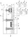
[0025]도 1은, 본원에 설명되는 증착을 수행하는 데 사용될 수 있는 원자 층 증착(ALD) 챔버(100)의 개략적인 횡단면도이다. 다른 증착 시스템들이 대안적으로 활용될 수 있다는 것이 고려된다. ALD 증착 프로세스는, 본원에 설명된 바와 같은 디스플레이 디바이스들에서, 유전체 층, 이를테면, 절연 층, 게이트 절연 층, 에칭 정지 층, 층간(interlayer) 절연체, 커패시터에 대한 유전체 층, 또는 패시베이션(passivation) 층을 형성하는 데 활용될 수 있다. 챔버(100)는 일반적으로, 챔버 바디(body)(101), 리드(lid) 조립체(104), 기판 지지 조립체(106), 및 프로세스 키트(150)를 포함한다. 리드 조립체(104)는 챔버 바디(101) 상에 배치되고, 기판 지지 조립체(106)는 챔버 바디(101) 내에 적어도 부분적으로 배치된다. 챔버 바디(101)는, 프로세싱 챔버(100)의 내부로의 액세스를 제공하도록 챔버 바디(101)의 측벽에 형성되는 슬릿 밸브 개구(108)를 포함한다. 일부 실시예들에서, 챔버 바디(101)는, 진공 시스템(예컨대, 진공 펌프)과 유체 연통(fluid communication)하는 하나 이상의 애퍼쳐(aperture)들을 포함한다. 애퍼쳐들은, 챔버(100) 내의 가스들에 대한 출구를 제공한다. 진공 시스템은, ALD 프로세스들에 적절한 프로세싱 챔버(100) 내의 압력을 유지하도록 프로세스 제어기에 의해 제어된다. 리드 조립체(104)는, 하나 이상의 차동 펌프들 및 퍼지(purge) 조립체들(120)을 포함할 수 있다. 차동 펌프 및 퍼지 조립체들(120)은 벨로우즈(bellows)(122)와 함께 리드 조립체(104)에 장착된다. 벨로우즈(122)는, 펌프 및 퍼지 조립체들(120)이, 가스 누설들에 대한 시일(seal)을 계속 유지하면서 리드 조립체(104)에 대해 수직으로 이동하는 것을 허용한다. 프로세스 키트(150)가 프로세싱 포지션으로 상승될 때, 프로세스 키트(150) 상의 컴플라이언트(compliant) 제1 시일(186) 및 컴플라이언트 제2 시일(188)은 차동 펌프 및 퍼지 조립체들(120)과 접촉하게 된다. 차동 펌프 및 퍼지 조립체들(120)은 진공 시스템(도시되지 않음)과 연결되어 낮은 압력에서 유지된다.[0025] FIG. 1 is a schematic cross-sectional view of an atomic layer deposition (ALD)
[0026]도 1에 도시된 바와 같이, 리드 조립체(104)는, 챔버(100) 내에 그리고/또는 프로세스 키트(150) 내에 반응성 종들(reactive species)의 플라즈마를 생성할 수 있는 RF 캐소드(110)를 포함한다. RF 캐소드(110)는, 예컨대 전기 가열 엘리먼트들(도시되지 않음)에 의해 가열되고 그리고 예컨대 냉각 유체들의 순환에 의해 냉각될 수 있다. 가스들을 반응성 종들로 활성화하고 그리고 반응성 종들의 플라즈마를 유지할 수 있는 임의의 전력 소스가 사용될 수 있다. 예컨대, RF 또는 MW(microwave) 기반 전력 디스차지(discharge) 기법들이 사용될 수 있다. 활성화는 또한, 열 기반 기법, 가스 분해(breakdown) 기법, 고강도 광원(예컨대, UV 에너지), 또는 x-선 소스에 대한 노출에 의해 발생될 수 있다.As shown in FIG. 1, the
[0027]기판 지지 조립체(106)는 챔버 바디(101) 내에 적어도 부분적으로 배치될 수 있다. 기판 지지 조립체(106)는, 챔버 바디 내에서의 프로세싱을 위해 기판(102)을 지지하기 위한 기판 지지 부재 또는 서셉터(susceptor)(130)를 포함할 수 있다. 서셉터(130)는, 챔버 바디(101)의 최하부 표면에 형성된 하나 이상의 개구들(126)을 통해 연장되는 샤프트(124) 또는 샤프트들(124)을 통해 기판 리프트 메커니즘(도시되지 않음)에 커플링될 수 있다. 기판 리프트 메커니즘은, 샤프트들(124) 주위로부터의 진공 누설을 방지하는 벨로우즈(128)에 의해 챔버 바디(101)에 플렉서블하게(flexibly) 시일링될 수 있다. 기판 리프트 메커니즘은, 서셉터(130)가, 도시된 바와 같은 하부 로봇 진입 포지션과, 프로세싱, 프로세스 키트 이송, 및 기판 이송 포지션들 사이로, ALD 챔버(100) 내에서 수직으로 이동되는 것을 허용한다. 일부 실시예들에서, 기판 리프트 메커니즘은 설명된 것들보다 더 적은 포지션들 사이에서 이동한다.The
[0028]일부 실시예들에서, 기판(102)은, 진공 척(chuck)(도시되지 않음), 정전 척(도시되지 않음), 또는 기계식 클램프(도시되지 않음)를 사용하여 서셉터에 고정될 수 있다. 서셉터(130)의 온도는, 기판(102) 및 프로세스 키트(150)의 온도에 영향을 주어 ALD 프로세싱의 성능을 개선하기 위해, ALD 챔버(100)에서의 프로세싱 동안 (예컨대, 프로세스 제어기에 의해) 제어될 수 있다. 서셉터(130)는, 예컨대, 서셉터(130) 내의 전기 가열 엘리먼트들(도시되지 않음)에 의해 가열될 수 있다. 서셉터(130)의 온도는, 예컨대, 챔버(100)의 고온계(pyrometer)들(도시되지 않음)에 의해 결정될 수 있다.[0028] In some embodiments, the
[0029]도 1에 도시된 바와 같이, 서셉터(130)는, 하나 이상의 리프트 핀들(136)을 수용하기 위해, 서셉터(130)를 통한 하나 이상의 보어(bore)들(134)을 포함할 수 있다. 각각의 리프트 핀(136)은, 리프트 핀(136)이 보어(134) 내에서 자유롭게 슬라이딩(slide)할 수 있도록 장착된다. 지지 조립체(106)는, 지지 조립체(106)가 하부 포지션에 있을 때, 리프트 핀들(136)의 상부 표면이 서셉터(130)의 기판 지지 표면(138) 위에 로케이팅될 수 있도록 이동가능하다. 반대로, 리프트 핀들(136)의 상부 표면은, 지지 조립체(106)가 상승된 포지션에 있을 때, 서셉터(130)의 기판 지지 표면(138) 아래에 로케이팅된다. 챔버 바디(101)에 접촉할 때, 리프트 핀들(136)은, 기판(102)의 하부 표면을 밀어서 서셉터(130)로부터 기판을 리프팅(lifting)한다. 반대로, 서셉터(130)는 기판(102)을 리프트 핀들(136)로부터 상승시킬 수 있다.As shown in FIG. 1, the
[0030]일부 실시예들에서, 서셉터(130)는, 하나 이상의 컴플라이언트 시일들(139)을 포함할 수 있는 프로세스 키트 절연 버튼들(137)을 포함한다. 프로세스 키트 절연 버튼들(137)은, 서셉터(130) 상에 프로세스 키트(150)를 전달하는 데 사용될 수 있다. 프로세스 키트 절연 버튼들(137)의 하나 이상의 컴플라이언트 시일들(139)은, 서셉터가 프로세스 키트(150)를 프로세싱 포지션으로 리프팅할 때 압축된다.In some embodiments, the
[0031]도 2는, 디스플레이 디바이스들, 이를테면, 박막 트랜지스터 디바이스들 또는 OLED 디바이스들에서 사용하기에 적절한 높은 유전 상수 재료 층을 형성하기 위한 프로세스(200)의 일 실시예의 흐름도를 도시한다. 그러한 높은 유전 상수 재료 층은, 커패시터를 형성하기 위한 2개의 금속 층들 사이에 배치되는 커패시터 층으로서 형성될 수 있다. 디스플레이 디바이스들에서 사용되는 높은 유전 상수 재료 층의 적절한 예들은, 게이트 절연 층, 2개의 금속 층들 사이에 배치되는 커패시터 층, 계면 층, 커패시터를 형성하는 데 활용되는 유전체 층, 에칭 정지 층 또는 패시베이션 층 ― 여기에는 절연 재료가 필요함 ― 을 포함한다. 높은 유전 상수 재료 층은, 도 1에 설명된 바와 같은 프로세싱 챔버(100) 또는 다른 적절한 프로세싱 챔버에서 실시될 수 있는 원자 층 증착(ALD) 프로세스 또는 플라즈마 보조 원자 층 증착(ALD) 프로세스(PE-ALD) 또는 이들의 조합에 의해 형성될 수 있다.[0031] FIG. 2 shows a flow diagram of one embodiment of a
[0032]프로세스(200)는, 동작(202)에서, 도 3a에 도시된 바와 같이, 높은 유전 상수 재료 층을 형성하기 위해, 프로세싱 챔버, 이를테면, 도 1에 도시된 프로세싱 챔버(100)(ALD 챔버) 내로 기판(102)을 이송함으로써 시작된다. 기판(102)은, 기판(102) 상에 상이한 디바이스 구조들 또는 상이한 막 스택(stack)들을 형성하는 것을 용이하게 하기 위해, 사전에 상부에 형성된 막들, 구조들, 또는 층들의 상이한 조합들을 가질 수 있다. 기판(102)은, 유리 기판, 플라스틱 기판, 폴리머 기판, 금속 기판, 단일화(singled) 기판, 롤-투-롤(roll-to-roll) 기판, 또는 박막 트랜지스터를 상부에 형성하기에 적절한 다른 적절한 투명 기판 중 임의의 것일 수 있다.[0032]
[0033]이어서, 동작(204)에서, 기판(102)의 표면(302) 상에 제1 층(304)을 형성함으로써 기판(102) 상에 높은 유전 상수 재료 층(308)(도 3c에 도시됨)을 형성하기 위해, 기판(102)에 대해 원자 층 증착(ALD) 프로세스가 수행된다. 제1 층(304)은, 도 3a에 도시된 바와 같이, 기판(102)의 상부 표면 상에, 반응성 가스상 종(gaseous species)과 함께 또는 반응성 가스상 종 없이, 제1 전구체를 공급하는 것에 의해 제1 반응을 수행함으로써 형성된다. 제1 층(304)은 무기 재료 함유 금속일 수 있다. 원자 층 증착(ALD) 프로세스는, 자기-종결/제한 성장(self-terminating/limiting growth)을 갖는 증착 프로세스이다. ALD 프로세스는, 증착의 각각의 주기(cycle)마다 단지 몇 옹스트롬 또는 단분자층(monolayer) 레벨의 두께를 생성한다. ALD 프로세스는, 프로세싱 챔버 내로 화학물질 및 반응물질을 순차적으로 분배함으로써 제어되며, 이는 주기적으로 반복된다. 기판(102) 상에 ALD 프로세스에 의해 형성될 높은 유전 상수 재료 층의 두께는 반응 사이클들의 횟수에 의존한다. 제1 전구체의 제1 반응은, 기판(102) 상에 흡착(adsorb)되는 분자 층의 제1 원자 층, 이를테면, 제1 층(304)을 제공하며, 제2 반응(동작(206)에서 아래에 추가로 설명될 것임)은, 제1 층(304) 상에 흡착되는 분자 층의 제2 원자 층, 이를테면, 도 3b에 도시된 제2 층(306)을 제공한다.[0033] Then, in
[0034]제1 반응은, 약 0.5 Å 내지 약 3 Å의 두께를 갖는 높은 유전 상수 재료 층(308)의 제1 층(304)을 증착할 수 있다.The first reaction may deposit a
[0035]일 예에서, 제1 층(304)을 형성하기 위한 반응의 제1 펄스(pulse)에서 활용되는 제1 전구체는, 지르코늄(Zr) 함유 전구체를 포함한다. 지르코늄 함유 전구체의 적절한 예들은, Zr-유기금속성 전구체들, 이를테면, 테트라키스(에틸메틸아미노)지르코늄(TEMAZ), 트리스(디메틸아미노)시클로펜타디에닐 지르코늄 (C5H5)Zr[N(CH3)2]3 등을 포함한다. 본원에서 활용되는 일 특정 예에서, 제1 전구체는 테트라키스(에틸메틸아미노)지르코늄(TEMAZ)이다.In one example, the first precursor utilized in the first pulse of the reaction to form the
[0036]원자 층 증착(ALD) 프로세스에 의해 높은 유전 상수 재료 층(308)으로서 Zr 함유 층을 형성하기 위해 Zr 함유 전구체를 활용하는 것은, 양호한 막 특성들, 이를테면, 높은 열적 안정성, 높은 증착률, 낮은 막 누설, 높은 막 밀도, 낮은 결함 밀도 등을 제공할 수 있는 것으로 여겨진다. 각각의 층들에서의 원자들의 강한 접착 및 기판의 표면 상으로의 원자들의 층들의 흡착성은, 전류 누설을 초래할 수 있는 유전체 층에서의 느슨한(loose) 막 구조를 효율적으로 제거할 수 있는 (화학 기상 증착 프로세스에 비해) 높은 막 밀도를 갖는 막 특성을 렌더링하도록, 컴팩트(compact)하고 안정된 결합 구조들을 막 구조들에 제공한다. 더욱이, 높은 막 밀도는 또한, 습기 또는 오염물이 그 막 구조들을 관통하는 것을 방지할 수 있다. 더욱이, 기판 상에 형성되는 단분자층들의 느린 ALD 증착률은 또한, 기판 표면 상의 막 결함들을 보수하는 것을 보조하기 위해, 기판 표면 상에 존재할 수 있는 핀홀(pinhole)들, 포어(pore)들, 피트(pit)들, 또는 결함들에 각각의 단분자층으로부터의 원자들이 점진적으로 충전되는 것을 허용한다.[0036] Utilizing a Zr-containing precursor to form a Zr-containing layer as a high dielectric
[0037]반응의 제1 펄스는, 미리 결정된 시간 인터벌(interval) 동안 지속된다. 본원에서 사용되는 바와 같은 펄스라는 용어는, 프로세스 챔버 내에 주입되는 재료의 도우즈(dose)를 지칭한다. 제1 전구체 또는/및 제2 전구체 및/또는 반응성 가스상 종의 각각의 펄스 사이에, 기판 표면과 미반응된/기판 표면에 의해 미-흡착된 부산물들, 불순물들, 또는 잔류 전구체 가스 혼합물(예컨대, 반응물질 가스 혼합물로부터의 미반응 불순물들 또는 다른 것들)을 제거하여 그들이 프로세싱 챔버 밖으로 펌핑될 수 있게 하기 위해, 제1 전구체 또는/및 제2 전구체 및/또는 반응성 가스상 종의 각각의 또는 다수의 펄스들 사이(예컨대, 상이한 금속 함유 가스와 산소 함유 가스 사이)에 퍼지 가스 혼합물, 이를테면, 질소 가스, 불활성 가스(예컨대, He 또는 Ar)가 프로세싱 챔버 내로 펄싱(pulse)될 수 있다.[0037] The first pulse of the reaction lasts for a predetermined time interval. The term pulse, as used herein, refers to the dose of material injected into the process chamber. Between each pulse of the first precursor or/and the second precursor and/or reactive gaseous species, by-products, impurities, or residual precursor gas mixtures (e.g., unreacted/un-adsorbed by the substrate surface) , Each or multiple of the first precursor or/and the second precursor and/or reactive gaseous species to remove unreacted impurities or others from the reactant gas mixture so that they can be pumped out of the processing chamber. A purge gas mixture, such as nitrogen gas, an inert gas (eg, He or Ar), may be pulsed into the processing chamber between pulses (eg, between different metal-containing gases and oxygen-containing gases).
[0038]증착 프로세스 동안 제1 층(304)을 형성하기 위해, Zr 함유 전구체를 포함하는 제1 전구체의 펄싱 동안, 반응성 가스상 종이 제1 전구체(예컨대, 일 예로서, Zr 함유 전구체)와 동시에, 교번적으로(alternatively), 또는 순차적으로 공급될 수 있다. 일 예에서, 제1 전구체와 동시에, 교번적으로, 또는 순차적으로 공급되는 반응성 가스상 종은, 산소 함유 가스들, 이를테면, H2O, O2, O3, CO2, H2O2, NO2, N2O 등일 수 있다. 일 예에서, 산소 함유 가스는 O2 또는 O3이다. 대안적으로, 반응성 가스상 종은, 프로세싱 챔버(100)에 남아 있는 잔류 제1 전구체를 퍼지 아웃(purge out)하기 위해 펌프/퍼지 가스의 펄스가 수행된 이후 공급될 수 있다.To form the
[0039]반응성 가스상 종과 함께 또는 반응성 가스상 종 없이(예컨대, 제1 전구체 이후 반응성 가스상 종이 공급됨), 제1 전구체의 펄싱 동안, 몇몇 프로세스 파라미터들이 또한 조정된다. 일 실시예에서, 프로세스 압력은, 약 0.1 Torr 내지 약 1 Torr로 제어된다. 프로세싱 온도는, 약 섭씨 40 도 내지 약 섭씨 300 도, 이를테면, 약 섭씨 200 도이다. 일 실시예에서, RF 소스 전력은, 약 500 와트 내지 약 3500 와트, 이를테면 약 3000 와트로 제어된다.[0039] During pulsing of the first precursor, with or without the reactive gaseous species (eg, the reactive gaseous species are supplied after the first precursor), several process parameters are also adjusted. In one embodiment, the process pressure is controlled from about 0.1 Torr to about 1 Torr. The processing temperature is about 40 degrees Celsius to about 300 degrees Celsius, such as about 200 degrees Celsius. In one embodiment, the RF source power is controlled from about 500 watts to about 3500 watts, such as about 3000 watts.
[0040]따라서, 도 3a에 도시된 제1 층(304)은, 반응성 가스상 종뿐만 아니라 제1 전구체의 제1 펄스 이후, 산소 엘리먼트들뿐만 아니라 Zr 엘리먼트들을 포함할 수 있다. 제1 층(304)은 Zr을 포함하고, 산소 엘리먼트들은 높은 유전 상수 재료 층(308)의 제1 부분을 형성한다.Accordingly, the
[0041] 동작(206)에서, 제1 반응 및 펌프/퍼지 프로세스 이후, 도 3b에 도시된 바와 같이, 제1 층(304)에 대한, 반응성 가스상 종과 함께 또는 반응상 가스상 종 없이, 제2 전구체를 포함하는 제2 반응이, 기판(102) 상에 제2 층(306)을 형성한다. 제2 전구체가 또한 금속 함유 전구체이지만 제1 전구체와 상이하다. 일 예에서, 제2 전구체는 알루미늄을 포함한다. 알루미늄을 포함하는 제2 전구체의 적절한 예들은, RxAlyR'zR''v 또는 RxAly(OR')z의 화학식을 가질 수 있으며, 여기서, R, R', 및 R''는 H, CH3, C2H5, C3H7, CO, NCO, 알킬 또는 아릴 기이고, x, y, z 및 v는 1 내지 8의 범위를 갖는 정수들이다. 다른 실시예에서, 알루미늄 함유 화합물은 Al(NRR')3의 화학식을 가질 수 있으며, 여기서, R 및 R'는 H, CH3, C2H5, C3H7, CO, NCO, 알킬 또는 아릴 기일 수 있고, R'는 H, CH3, C2H5, C3H7, CO, NCO, 알킬 또는 아릴 기일 수 있다. 적절한 알루미늄 함유 화합물들의 예들은, 디에틸알루미늄 에톡시드(Et2AlOEt), 트리에틸-트리-2차-부톡시 다이알루미늄(Et3Al2OBu3, 또는 EBDA), 트리메틸알루미늄(TMA), 트리메틸다이알루미늄 에톡시드, 디메틸 알루미늄 이소프로폭시드, 디케부톡시 알루미늄 에톡시드, (OR)2AlR'이며, 여기서, R, R', 및 R''는 메틸, 에틸, 프로필, 이소프로필, 부틸, 이소부틸, 3차 부틸, 및 더 많은 수의 탄소 원자들을 갖는 다른 알킬 기들 등일 수 있다.[0041] In
[0042]일 특정 예에서, 알루미늄을 포함하는 제2 전구체는 트리메틸알루미늄(TMA)이다.In one specific example, the second precursor comprising aluminum is trimethylaluminum (TMA).
[0043]각각의 반응은, 약 0.5 Å 내지 약 3 Å의 두께를 갖는 높은 유전 상수 재료 층(308)의 제2 층(306)을 증착할 수 있다.Each reaction may deposit a
[0044]제2 전구체로부터 제공되는 제2 금속 엘리먼트들은, 비정질 구조의 결과적인 높은 유전 상수 재료 층(308)을 렌더링하기 위해 높은 유전 상수 재료 층(308)에 도핑되는 도펀트로서 고려될 수 있는 것으로 여겨진다. 원자 층 증착 프로세스에 의해 형성되는 ZrO2 층은 종종, 적어도 약 25 내지 약 50의 유전 상수를 제공하는, 입방정계 또는 정방정계 위상의 결정질(crystalline) 구조로 결과적인 ZrO2를 제공한다. 그러나, 재료의 유전 상수가 증가함에 따라, 재료의 밴드 갭(band gap)이 감소되어, 디바이스에서 높은 누설 전류가 유발된다. 따라서, 재료에 도펀트(이를테면, 제2 엘리먼트)를 제공함으로써, 재료의 결정질 구조가 비정질 상태로 변경될 수 있으며, 그에 따라, 특정한 미리 결정된 레벨의 유전 상수를 낮추어, 전류 누설이 원하는 낮은 레벨로 유지된다. 예컨대, ZrO2 구조 내에 도펀트(이를테면, 알루미늄을 포함하는 제2 금속 엘리먼트)를 제공함으로써, 결과적인 ZrO2 구조를 비정질이 되게 할 수 있으며, 그에 따라, 비정질 알루미늄 도핑된 ZrO2의 유전 상수가 약 15 내지 약 25의 범위로 유지된다.[0044] The second metal elements provided from the second precursor can be considered as a dopant doped to the high dielectric
[0045]제2 반응은, 미리 결정된 시간 인터벌 동안 지속되어 알루미늄을 포함하는 제2 층(306)을 형성한다. 증착 프로세스 동안 제2 층(306)을 형성하기 위해, Al 함유 전구체를 포함하는 제2 전구체의 펄싱 동안, 반응성 가스상 종이 제2 전구체(예컨대, 일 예로서, Al 함유 전구체)와 동시에, 교번적으로, 또는 순차적으로 공급될 수 있다. 일 예에서, 제1 전구체와 동시에, 교번적으로, 또는 순차적으로 공급되는 반응성 가스상 종은, 산소 함유 가스들, 이를테면, H2O, O2, O3, CO2, H2O2, NO2, N2O 등일 수 있다. 일 예에서, 산소 함유 가스는 O2 또는 O3이다. 대안적으로, 반응성 가스상 종은, 프로세싱 챔버(100)에 남아 있는 잔류 제2 전구체를 퍼지 아웃하기 위해 펌프/퍼지 가스의 펄스가 수행된 이후 공급될 수 있다.[0045] The second reaction lasts for a predetermined time interval to form a
[0046]반응성 가스상 종과 함께 또는 반응성 가스상 종 없이(예컨대, 제2 전구체 이후 반응성 가스상 종이 공급됨), 제2 전구체의 공급 동안, 몇몇 프로세스 파라미터들이 또한 조정된다. 일 실시예에서, 프로세스 압력은, 약 0.1 Torr 내지 약 1 Torr로 제어된다. 프로세싱 온도는, 약 섭씨 40 도 내지 약 섭씨 300 도, 이를테면, 약 섭씨 200 도이다. RF 소스 전력은, 약 500 와트 내지 약 3500 와트, 이를테면 약 3000 와트로 제어된다.[0046] During the supply of the second precursor, with or without the reactive gaseous species (eg, the reactive gaseous species are supplied after the second precursor), several process parameters are also adjusted. In one embodiment, the process pressure is controlled from about 0.1 Torr to about 1 Torr. The processing temperature is about 40 degrees Celsius to about 300 degrees Celsius, such as about 200 degrees Celsius. The RF source power is controlled from about 500 watts to about 3500 watts, such as about 3000 watts.
[0047]따라서, 도 3b에 도시된 제2 층(306)은, 반응성 가스상 종뿐만 아니라 제2 전구체의 제2 펄스 이후, 산소 엘리먼트들뿐만 아니라 Al 엘리먼트들을 포함할 수 있다. 제2 층(306)은 Al을 포함하고, 산소 엘리먼트들은 높은 유전 상수 재료 층(308)의 제2 부분을 형성한다.Thus, the
[0048]동작(204)에서의 제1 반응 및 동작(206)에서의 제2 반응은, 전체 높은 유전 상수 재료 층(308)의 원하는 두께에 도달할 때까지 (루프(207)로 표시된 바와 같이) 반복적으로 수행되어, 최상부 제1 층(304') 및 최상부 제2 층(306')을 형성할 수 있다는 것이 유의된다.[0048] The first reaction in
[0049]동작(208)에서, 동작(204 및 206)에서의 반응들의 제1 펄스 및 제2 펄스의 다수의 반복되는 사이클들 이후, 이어서, 도 3c에 도시된 바와 같이, 높은 유전 상수 재료 층(308)이 기판 상에 형성된다. 일 예에서, 높은 유전 상수 재료 층(308)을 형성하기 위해, 총 약 200 사이클들의 동작(204 및 206)이 수행될 수 있다. 결과적인 높은 유전 상수 재료 층(308)은, 원하는 두께(310)에 도달할 때까지의 반복되는 제1 및 제2 층들(최하부 제1 및 제2 층(304, 306), 및 최상부 제1 및 제2 층(304', 306'로 도시됨))의 다수의 층들을 포함할 수 있다. 일 예에서, 원하는 두께(310)는 약 25 nm 내지 약 90 nm일 수 있다. 높은 유전 상수 재료 층(308)은, 약 15 내지 25의 유전 상수, 및 약 1E-8A/cm2 또는 그 미만의 막 누설을 가질 수 있다. 높은 유전 상수 재료 층(308)은, 6 atm. % 내지 약 20 atm. %(Zr과 Al의 엘리먼트들 사이)의 도핑 농도로 ZrO2 구조에 알루미늄 도펀트를 갖는다.[0049] In
[0050]증착 프로세스(200)는, 유전 상수가 10보다 큰, 이를테면, 15보다 큰, 예컨대, 약 15 내지 25인 높은 유전 상수 재료 층을 형성한다. 일 예에서, 결과적인 높은 유전 상수 재료 층(308)은, 비정질 구조를 갖는 Al 도펀트들을 가진 ZrO2 층이다.The
[0051]도펀트는, 높은 유전 상수 재료 층(308)에서 초래되는 유전 상수의 범위에 영향을 미칠 수 있다는 것이 유의된다. 일 예에서, ZrO2 구조의 알루미늄 도펀트가 (Zr과 Al의 엘리먼트들 사이의) 5 atm. % 미만으로 제어될 수 있는 도핑 농도를 가질 때, 이는, 약 25 내지 45의 유전 상수를 갖는 실질적으로 결정질 구조의 구조를 가진 높은 유전 상수 재료 층(308)을 초래할 수 있다. 다른 예에서, 6 atm. % 내지 약 20 atm. %(Zr과 Al의 엘리먼트들 사이)로 제어될 수 있는 도핑 농도를 갖는 ZrO2 구조의 알루미늄 도펀트는, 약 15 내지 25의 유전 상수를 갖는 비정질 구조의 구조를 가진 높은 유전 상수 재료 층(308)을 초래할 수 있다. 또 다른 예에서, 20 atm. % 내지 약 100 atm. %(Zr과 Al의 엘리먼트들 사이)로 제어될 수 있는 도핑 농도를 갖는 ZrO2 구조의 알루미늄 도펀트는, 약 9 내지 15의 유전 상수를 갖는 비정질 구조의 구조를 가진 높은 유전 상수 재료 층(308)을 초래할 수 있다.It is noted that the dopant can affect the range of dielectric constants resulting in the high dielectric
[0052]일부 예들에서, 높은 유전 상수 재료 층(308)의 Al 도펀트들은 또한 실리콘 도펀트들로 대체될 수 있다. 예컨대, 실리콘 함유 도펀트, 이를테면 SiO2가 또한, 유전 상수가 15보다 큰, 예컨대, 약 15 내지 25인 막 층을 형성하기 위해 ZrO2 재료에서 사용될 수 있다.[0052] In some examples, the Al dopants of the high dielectric
[0053]도 4는, 디스플레이 디바이스들, 이를테면, 박막 트랜지스터 디바이스들 또는 OLED 디바이스들에서 사용하기에 적절한, 높은 유전 상수뿐만 아니라 낮은 막 누설을 갖는 복합 막 층을 형성하기 위한 프로세스(400)의 일 실시예의 흐름도를 도시한다. 높은 유전 상수를 갖는 그러한 복합 막 층은, 커패시터를 형성하기 위한 2개의 금속 층들 사이에 배치되는 커패시터 층으로서 형성될 수 있다. 디스플레이 디바이스들에서 사용되는 높은 유전 상수를 갖는 복합 막 층의 적절한 예들은, 게이트 절연 층, 2개의 금속 층들 사이에 배치되는 커패시터 층, 계면 층, 커패시터를 형성하는 데 활용되는 유전체 층, 에칭 정지 층 또는 패시베이션 층 ― 여기에는 절연 재료가 필요함 ― 을 포함한다. 높은 유전 상수 재료 층은, 도 1에 설명된 바와 같은 프로세싱 챔버(100) 또는 다른 적절한 프로세싱 챔버에서 실시될 수 있는 원자 층 증착(ALD) 프로세스 또는 플라즈마 보조 원자 층 증착 프로세스(PE-ALD) 또는 이들의 조합에 의해 형성될 수 있다.[0053] FIG. 4 is an illustration of a
[0054]프로세스(400)는, 동작(402)에서, 도 5a에 도시된 바와 같이, 기판(102) 상에 높은 유전 상수를 갖는 복합 막 층(502)을 형성하기 위해, 프로세싱 챔버, 이를테면, 도 1에 도시된 프로세싱 챔버(100)(ALD 챔버) 내로 기판(102)을 이송함으로써 시작된다.
[0055]이어서, 동작(404)에서, 도 5a에 도시된 바와 같이, 복합 막 층(502)의 제1 층(510)을 형성하기 위해, 원자 층 증착(ALD) 프로세스가 기판(102)에 대해 수행된다. 복합 막 층(502)의 제1 층(510)은, ALD 프로세스에 의해 형성될 수 있다. 제1 층(510)은, 도 5a에 도시된 바와 같이, 기판(102) 상에, 반응성 가스상 종과 함께 또는 반응성 가스상 종 없이, 전구체 가스 혼합물들(하나 초과의 타입의 전구체 가스 혼합물들)을 연속적으로 펄싱하는 것에 의해, ALD 프로세스의 제1 타입의 반응을 수행함으로써 형성될 수 있으며, 제1 층(510)을 형성하는 것은 무기 재료 함유 금속일 수 있다. 반응성 가스상 종은, 전구체 가스 혼합물들과 동시에, 교번적으로, 또는 순차적으로 펄싱되어 복합 막 층(502)의 제1 층(510)을 형성할 수 있다는 것이 유의된다. 전구체 가스 혼합물들 및 반응성 가스상 종의 펄스들 사이에, 다른 펄스 이전에 프로세싱 챔버로부터 전구체 잔류물들을 제거하기 위해 펌프/퍼지 프로세스가 수행될 수 있다.[0055] Then, in
[0056] 기판(102) 상에 ALD 프로세스에 의해 형성될 복합 막 층(502)의 두께(화살표(506)로 나타냄)는 반응 사이클들의 횟수에 의존한다. 일 예에서, 복합 막 층(502)의 제1 층(510)은 약 25 nm 내지 약 90 nm의 두께를 갖는다.[0056] The thickness of the
[0057]일 예에서, 제1 층(510)을 형성하는 데 활용되는 전구체 혼합물들은, 알루미늄 도핑된 지르코늄(Zr) 함유 층을 형성하기 위해, 반응성 가스상 종과 함께 또는 반응성 가스상 종 없이, 지르코늄 함유 전구체 및 알루미늄 함유 전구체를 교번적으로 또는 순차적으로 공급하는 것을 포함할 수 있다. 적절한 지르코늄 함유 전구체는, Zr-유기금속성 전구체들, 이를테면, 테트라키스(에틸메틸아미노)지르코늄(TEMAZ), 트리스(디메틸아미노)시클로펜타디에닐 지르코늄 (C5H5)Zr[N(CH3)2]3 등을 포함한다. 본원에서 활용되는 일 특정 예에서, 지르코늄 함유 전구체는 테트라키스(에틸메틸아미노)지르코늄(TEMAZ)이다.[0057] In one example, the precursor mixtures utilized to form the
[0058]알루미늄 함유 전구체의 적절한 예들은, RxAlyR'zR''v 또는 RxAly(OR')z의 화학식을 가질 수 있으며, 여기서, R, R', 및 R''는 H, CH3, C2H5, C3H7, CO, NCO, 알킬 또는 아릴 기이고, x, y, z 및 v는 1 내지 8의 범위를 갖는 정수들이다. 다른 실시예에서, 알루미늄 함유 화합물은 Al(NRR')3의 화학식을 가질 수 있으며, 여기서, R 및 R'는 H, CH3, C2H5, C3H7, CO, NCO, 알킬 또는 아릴 기일 수 있고, R'는 H, CH3, C2H5, C3H7, CO, NCO, 알킬 또는 아릴 기일 수 있다. 적절한 알루미늄 함유 화합물들의 예들은, 디에틸알루미늄 에톡시드(Et2AlOEt), 트리에틸-트리-2차-부톡시 다이알루미늄(Et3Al2OBu3, 또는 EBDA), 트리메틸알루미늄(TMA), 트리메틸다이알루미늄 에톡시드, 디메틸 알루미늄 이소프로폭시드, 디케부톡시 알루미늄 에톡시드, (OR)2AlR'이며, 여기서, R, R', 및 R''는 메틸, 에틸, 프로필, 이소프로필, 부틸, 이소부틸, 3차 부틸, 및 더 많은 수의 탄소 원자들을 갖는 다른 알킬 기들 등일 수 있다. 일 특정 예에서, 알루미늄 함유 전구체는 트리메틸알루미늄(TMA)이다.[0058] Suitable examples of aluminum-containing precursors, Rx Aly R'z R''v or Rx Aly (OR') can have the formula ofz, and wherein, R, R ', and R'' Is H, CH3 , C2 H5 , C3 H7 , CO, NCO, an alkyl or aryl group, and x, y, z and v are integers ranging from 1 to 8. In another embodiment, the aluminum-containing compound may have a formula of Al(NRR')3 , wherein R and R'are H, CH3 , C2 H5 , C3 H7 , CO, NCO, alkyl or It can be an aryl group, and R'can be H, CH3 , C2 H5 , C3 H7 , CO, NCO, alkyl or aryl group. Examples of suitable aluminum-containing compounds are diethylaluminum ethoxide (Et2 AlOEt), triethyl-tri-secondary-butoxy dialuminate (Et3 Al2 OBu3 , or EBDA), trimethylaluminum (TMA), trimethyl Dialluminum ethoxide, dimethyl aluminum isopropoxide, dikebutoxy aluminum ethoxide, (OR)2 AlR', wherein R, R', and R'' are methyl, ethyl, propyl, isopropyl, butyl, Isobutyl, tertiary butyl, and other alkyl groups having a higher number of carbon atoms, and the like. In one specific example, the aluminum containing precursor is trimethylaluminum (TMA).
[0059]반응성 가스상 종은, 산소 함유 가스들, 이를테면, H2O, O2, O3, H2O2, CO2, NO2, N2O 등일 수 있다. 일 예에서, 산소 함유 가스는 O2 또는 O3이다.[0059] The reactive gaseous species may be oxygen-containing gases, such as H2 O, O2 , O3 , H2 O2 , CO2 , NO2 , N2 O, and the like. In one example, the oxygen containing gas is O2 or O3 .
[0060]제1 층(510)(예컨대, Zr 함유 층)에 형성 및 도핑되는 제2 금속 엘리먼트들, 예컨대, 알루미늄 함유 도펀트들은, 비정질 구조로서 ZrO2 층의 제1 층(510)을 렌더링하기 위해 복합 막 층(502)에 도핑되는 도펀트들로서 고려될 수 있는 것으로 여겨진다. 원자 층 증착 프로세스에 의해 형성되는 ZrO2 층은 종종, 적어도 25보다 큰, 이를테면, 약 25 내지 약 50의 유전 상수를 제공하는, 입방정계 위상 또는 정방정계 위상 또는 입방정계 위상과 정방정계 위상의 혼합으로 이루어진 결정질 구조의 ZrO2를 제공한다. 그러나, 재료의 유전 상수가 증가함에 따라, 재료의 밴드 갭이 감소되어, 디바이스에서 높은 누설 전류가 유발된다. 따라서, 첨단 기술에 대해, 더 높은 커패시턴스를 갖는 커패시터를 제공하기 위해서는 유전체 층의 더 높은(예컨대, 25보다 큰) 유전 상수가 바람직하다. 대조적으로, 유전체 층의 더 높은(예컨대, 25보다 큰) 유전 상수는 또한 높은 막 누설을 종종 초래하며, 이는 결국, 디바이스 장애를 유발할 수 있다. 따라서, 비교적 낮은(예컨대, 10보다 크지만 25보다는 작은) 유전 상수를 갖는, 복합 막 층(502)의 제1 층(510)을 형성함으로써, 복합 막 층(502)이 특정 정도의 낮은 막 누설을 유지할 수 있다. 따라서, 복합 막 층(502)의 제1 층(510)에 형성되는 도펀트(이를테면, 알루미늄 도펀트들)를 제공함으로써, 재료의 결정질 구조가 비정질 상태로 변경될 수 있으며, 그에 따라, 특정한 미리 결정된 레벨의 유전 상수를 낮추어, 전류 누설이 원하는 낮은 레벨로 유지된다. 예컨대, 제1 층(510)을 형성하기 위해 ZrO2 구조 내에 알루미늄 도펀트를 제공함으로써, 결과적인 ZrO2 구조를 비정질 상태로 렌더링할 수 있으며, 그에 따라, 비정질 알루미늄 도핑된 ZrO2의 유전 상수가 25보다 작지만 10을 초과하는 원하는 범위로 유지된다. 후속하여, 동작(406)에서 아래에 상세히 설명될 바와 같이, 결과적인 복합 막 층(502)의 커패시턴스를 증가시키기 위해, 입방정계 위상 또는 정방정계 위상 또는 입방정계 위상과 정방정계 위상의 혼합으로 이루어진 결정질 구조의 ZrO2(예컨대, 25보다 큰 유전 상수)에 의해 복합 막 층(502)의 제2 층(512)이 형성된다.[0060] Second metal elements formed and doped in the first layer 510 (eg, a Zr-containing layer), such as aluminum-containing dopants, to render the
[0061] 일 예에서, 제1 층(510)을 형성하기 위한 제1 타입의 반응에서 공급되는 전구체 가스 혼합물들은, 반응성 가스상 종으로서 산소 함유 가스와 함께 또는 산소 함유 가스 없이, Zr 함유 전구체를 포함하는 제1 전구체를 펄싱하는 것을 포함한다. 산소 함유 가스가 Zr 함유 전구체와 함께 공급되지 않는 예에서, 산소 함유 가스는, Zr 함유 전구체가 프로세싱 챔버(100)에 공급된 이후 그리고 펌프/퍼지 프로세스 이후 공급될 수 있다. Zr 함유 전구체를 포함하는 제1 전구체가 펄싱된 이후, 이어서, Al 함유 전구체를 포함하는 제2 전구체가 펄싱되어 제1 층(510)을 형성하는 것을 계속할 수 있어서, 알루미늄 도핑된 ZrO2 층으로서 제1 층(510)이 형성된다. 유사하게, Al 함유 전구체를 포함하는 제2 전구체가 반응성 가스상 종으로서 산소 함유 가스와 함께 또는 산소 함유 가스 없이 공급될 수 있다. 산소 함유 가스가 Al 함유 전구체와 함께 공급되지 않는 예에서, 산소 함유 가스는, Al 함유 전구체가 프로세싱 챔버(100)에 공급된 이후 그리고 펌프/퍼지 프로세스 이후 공급될 수 있다. Zr 함유 전구체를 포함하는 제1 전구체 및 Al 함유 전구체를 포함하는 제2 전구체를 공급하는 시퀀스는 반전될 수 있거나 또는 필요에 따라 임의의 순서로 이루어질 수 있다는 것이 유의된다. 반응성 가스상 종은 항상, 제1 및 제2 전구체들의 각각의 펄스 사이에 공급되어 ZrO2 또는 Al 도핑된 ZrO2를 형성할 반응성 종으로서 기능한다는 것이 유의된다.[0061] In one example, the precursor gas mixtures supplied in the first type of reaction for forming the
[0062]동작(404)에서의 제1 타입의 반응의 펄스들은 미리 결정된 시간 인터벌 동안 지속된다. 본원에서 사용되는 바와 같은 펄스라는 용어는, 프로세스 챔버 내에 주입되는 재료의 도우즈를 지칭한다. 제1 전구체 또는/및 제2 전구체 및/또는 반응성 가스상 종의 각각의 펄스 사이에, 기판 표면과 미반응된/기판 표면에 의해 미-흡착된 부산물들, 불순물들, 또는 잔류 전구체 가스 혼합물(예컨대, 반응물질 가스 혼합물로부터의 미반응 불순물들 또는 다른 것들)을 제거하여 그들이 프로세싱 챔버 밖으로 펌핑될 수 있게 하기 위해, 제1 전구체 또는/및 제2 전구체 및/또는 반응성 가스상 종의 각각의 또는 다수의 펄스들 사이(예컨대, 상이한 금속 함유 가스와 산소 함유 가스 사이)에 퍼지 가스 혼합물, 이를테면, 질소 가스, 불활성 가스(예컨대, He 또는 Ar)가 프로세싱 챔버 내로 펄싱될 수 있다.Pulses of the first type of reaction in
[0063]복합 막 층(502)의 제1 층(510)은, 10보다 큰, 이를테면 15 내지 25의 유전 상수 및 약 1E-8A/cm2 또는 그 미만의 막 누설을 가질 수 있다. 복합 막 층(502)의 제1 층(510)은, 약 6 atm. % 내지 약 20 atm. %(Zr과 Al의 엘리먼트들 사이)의 도핑 농도로 ZrO2 구조에 알루미늄 도펀트를 갖는다.[0063] The
[0064]동작(404)에서 제1 층(510)을 형성하는 제1 타입의 반응 동안, 몇몇 프로세스 파라미터들이 또한 조정된다. 일 실시예에서, 프로세스 압력은, 약 0.1 Torr 내지 약 1 Torr로 제어된다. 프로세싱 온도는, 약 섭씨 40 도 내지 약 섭씨 300 도, 이를테면, 약 섭씨 200 도이다. RF 소스 전력은, 약 500 와트 내지 약 3500 와트, 이를테면 약 3000 와트로 제어된다.During the first type of reaction of forming the
[0065]도펀트는, 제1 층(510)에서 초래되는 유전 상수의 범위에 영향을 미칠 수 있다는 것이 유의된다. 일 예에서, ZrO2 구조의 알루미늄 도펀트가 (Zr과 Al의 엘리먼트들 사이의) 5 atm. % 미만으로 제어될 수 있는 도핑 농도를 가질 때, 이는, 약 25 내지 45의 유전 상수를 갖는 실질적으로 결정질 구조의 구조를 가진 결과적인 제1 층(510)을 초래할 수 있다. 다른 예에서, 5 atm. % 내지 약 20 atm. %(Zr과 Al의 엘리먼트들 사이)로 제어될 수 있는 도핑 농도를 갖는 ZrO2 구조의 알루미늄 도펀트는, 약 15 내지 25의 유전 상수를 갖는 비정질 구조의 구조를 가진 결과적인 제1 층(510)을 초래할 수 있다. 또 다른 예에서, 20 atm. % 내지 약 100 atm. %(Zr과 Al의 엘리먼트들 사이)로 제어될 수 있는 도핑 농도를 갖는 ZrO2 구조의 알루미늄 도펀트는, 약 9 내지 15의 유전 상수를 갖는 비정질 구조의 구조를 가진 결과적인 제1 층(510)을 초래할 수 있다.It is noted that the dopant can affect the range of dielectric constants resulting in the
[0066]일부 예들에서, 제1 층(510)의 Al 도펀트들은 또한 실리콘 도펀트들로 대체될 수 있다. 예컨대, 실리콘 함유 도펀트, 이를테면 SiO2가 또한, 유전 상수가 15보다 큰, 예컨대, 약 15 내지 25인 막 층을 형성하기 위해 ZrO2 재료에서 사용될 수 있다.In some examples, the Al dopants of the
[0067]동작(406)에서, 복합 막 층(502)의 제1 층(510)이 형성된 이후, 복합 막 층(502)을 형성하기 위해 수행되는 ALD 프로세스의 제2 타입의 반응에 의해 제1 층(510) 상에 제2 층(512)이 형성된다. 제2 층(512)은, 화살표들(514)로 나타낸 두께를 갖는다. 위에 논의된 바와 같이, 원하는 낮은 막 누설을 가지면서 원하는 높은 유전 상수 레벨로 결과적인 복합 막 층(502)을 유지하기 위해, 제2 층(512)은, 적어도 25보다 큰, 이를테면, 약 35 내지 약 50의 유전 상수를 제공하는, 입방정계 위상 또는 정방정계 위상 또는 입방정계 위상과 정방정계 위상의 혼합으로 이루어진 결정질 구조의 ZrO2 층을 주로 갖도록 형성된다. 원자 층 증착 프로세스에 의해 형성되는 ZrO2 층의 제2 층(512)은 종종, 비정질 및 결정질 구조들을 포함하는 원하는 2개-층 구조를 갖는 결과적인 복합 막 층(502)을 제공하기 위해, (예컨대, 입방정계 위상 및/또는 정방정계 위상 또는 이들의 결합들로 이루어진) 결정질 구조의 결과적인 ZrO2를 제공한다.[0067] In
[0068]최소 Al 도펀트 농도(예컨대, 5 원자 % 미만)를 제어함으로써, 제2 층(512)의 (예컨대, 입방정계 위상 및/또는 정방정계 위상 또는 이들의 결합들로 이루어진) 결정질 구조가 또한 획득될 수 있다는 것이 유의된다.[0068] By controlling the minimum Al dopant concentration (eg, less than 5 atomic %), the crystalline structure (eg, consisting of a cubic phase and/or a tetragonal phase or combinations thereof) of the
[0069]원자 층 증착(ALD) 프로세스에 의한 결과적인 복합 막 층(502)의 제2 층(312)으로서 Zr 함유 층을 활용하는 것은, 양호한 막 특성들, 이를테면, 높은 열적 안정성, 높은 증착률, 높은 막 밀도, 낮은 결함 밀도 등을 제공할 수 있는 것으로 여겨진다.[0069] Utilizing a Zr-containing layer as the second layer 312 of the resulting
[0070]일 예에서, 제2 층(512)을 형성하기 위한 제2 타입의 반응에서 공급되는 전구체 가스 혼합물은, 반응성 가스상 종으로서 산소 함유 가스와 함께 또는 산소 함유 가스 없이, Zr 함유 전구체를 포함하는 전구체를 펄싱하는 것을 포함한다. 산소 함유 가스가 Zr 함유 전구체와 함께 공급되지 않는 예에서, 산소 함유 가스는, Zr 함유 전구체가 프로세싱 챔버(100)에 공급된 이후 그리고 펌프/퍼지 프로세스 이후 공급될 수 있다.[0070] In one example, the precursor gas mixture supplied in the second type of reaction for forming the
[0071]증착 프로세스 동안 제2 층(512)을 형성하기 위해, Zr 함유 전구체를 포함하는 전구체의 공급 동안, 반응성 가스상 종이 전구체(예컨대, 일 예로서, Zr 함유 전구체)와 동시에, 교번적으로, 또는 순차적으로 공급될 수 있다. 반응성 가스상 종은, 프로세싱 챔버(100)에 남아 있는 잔류 제1 전구체를 퍼지 아웃하기 위해 펌프/퍼지 가스의 펄스가 수행된 이후 공급될 수 있다. 동작(406)에서의 제2 타입의 반응의 펄스들은 미리 결정된 시간 인터벌 동안 지속된다. 전구체 및/또는 반응성 가스상 종의 각각의 펄스 사이에, 기판 표면과 미반응된/기판 표면에 의해 미-흡착된 불순물들 또는 잔류 전구체 가스 혼합물(예컨대, 반응물질 가스 혼합물로부터의 미반응 불순물들 또는 다른 것들)을 제거하여 그들이 프로세싱 챔버 밖으로 펌핑될 수 있게 하기 위해, 전구체 및/또는 반응성 가스상 종의 각각의 또는 다수의 펄스들 사이(예컨대, 금속 함유 가스와 산소 함유 가스 사이)에 퍼지 가스 혼합물, 이를테면, 질소 가스, 불활성 가스(예컨대, He 또는 Ar)가 프로세싱 챔버 내로 펄싱될 수 있다. 반응성 가스상 종은 항상, 전구체의 각각의 펄스 사이에 공급되어 제2 층(512)으로서의 ZrO2를 형성할 반응성 종으로서 기능한다는 것이 유의된다.[0071] To form the
[0072]복합 막 층(502)의 제2 층(512)은, 25보다 큰, 이를테면 25 내지 50의 유전 상수를 가질 수 있다. 일 예에서, 복합 막 층(502)의 제2 층(512)은 약 25 nm 내지 약 90 nm의 두께를 갖는다.[0072] The
[0073]동작(406)에서 제2 층(512)을 형성하는 제2 타입의 반응 동안, 몇몇 프로세스 파라미터들이 또한 조정된다. 일 실시예에서, 프로세스 압력은, 약 0.1 Torr 내지 약 1 Torr로 제어된다. 프로세싱 온도는, 약 섭씨 40 도 내지 약 섭씨 300 도, 이를테면, 약 섭씨 200 도이다. RF 소스 전력은, 약 500 와트 내지 약 3500 와트, 이를테면 약 3000 와트로 제어된다.[0073] During the second type of reaction forming the
[0074]일 예에서, 제1 층(510)(예컨대, 알루미늄 도핑된 ZrO2 층)을 형성하기 위해 동작(404)에서 공급되는, 알루미늄을 포함하는 제2 전구체는, 제1 층(510)이 원하는 두께에 도달했을 때 공급이 제거될 수 있으며, 그에 따라, 지르코늄을 포함하는 제1 전구체가 (반응성 종과 함께 또는 반응성 종 없이) 계속해서 펄싱 및 공급되게 하여, 주로 지르코늄 산화물을 포함하는 제2 층(512)이 형성되게 한다. 반응성 가스상 종은 항상, Zr을 포함하는 제1 전구체 및/또는 Al을 포함하는 제2 전구체의 각각의 펄스 사이에 공급되어 ZrO2 또는 Al 도핑된 ZrO2를 형성할 반응성 종으로서 기능한다는 것이 유의된다.[0074] In one example, a second precursor comprising aluminum, supplied in
[0075]제1 층(510)과 제2 층(512) 간의 두께 비를 조정함으로써, 결과적인 복합 막 층(502)은, 약 15 내지 약 35의 평균 막 유전 상수를 가질 수 있다.By adjusting the thickness ratio between the
[0076]기판(102) 상에 형성되는 제1 층 및 제2 층(510, 512)의 순서는 임의의 순서로 이루어질 수 있거나 또는 가능한 한 여러 번 이루어질 수 있다는 것이 유의된다. 예컨대, 복합 막 층(502)은, 임의의 순서로, 필요한 만큼의 많은 반복되는 제1 층 및 제2 층(510, 512)을 가질 수 있다.It is noted that the order of the first and
[0077]일부 예들에서, 도 5a-5b의 복합 막 층(502) 또는 도 3a-3c의 높은 유전 상수 재료 층(308)은 또한, Zr 함유 층들보다는 알루미늄 함유 층들 또는 하프늄 함유 층들로서 형성될 수 있다.[0077] In some examples, the
[0078]일 예에서, 필요한 경우, 디바이스 구조의 높은 유전 상수 재료 층(308) 위, 또는 복합 막 층(502) 위, 또는 높은 유전 상수 재료 층(308)과 기판 사이, 또는 기판과 복합 막 층(502) 사이의 계면에 부가적인 알루미늄 함유 층(이를테면, Al2O3 및 Al2N3)이 형성될 수 있다.[0078] In one example, if necessary, over the high dielectric
[0079]부가적으로, 제1 층 및 제2 층(510, 512)의 계면, 위, 또는 아래에 부가적인 알루미늄 함유 층이 형성되는 대신, 도 5c에 도시된 바와 같이, 제2 층(512) 상에 부가적인 층(515)이 형성될 수 있다. 유사하게, 부가적인 층(515)은 또한, ALD 또는 PE-ALD 프로세스에 의해 형성될 수 있다. 위에 논의된 바와 같이, 원하는 낮은 막 누설을 가지면서 원하는 높은 유전 상수 레벨로 결과적인 복합 막 층(502)을 유지하기 위해, 제2 층(512) 상에 형성되는 부가적인 층(515)은 고도로(heavily) 알루미늄 도핑된 ZrO2 층일 수 있으며, 이는, 주로 알루미늄 산화물을 포함하는 비정질 상태인 부가적인 층(515)을 렌더링한다. 부가적인 층(515)은 약 9 내지 약 15의 유전 상수를 가질 수 있다. ZrO2 층의 Al의 농도는, 20 원자 % 초과, 이를테면, 약 20 원자 % 내지 약 100 원자 %이다.Additionally, instead of forming an additional aluminum-containing layer above, or below the interface of the first and
[0080]고도로 도핑된 ZrO2 층은, 도 5c에서 부가적인 층(517)으로서 점선으로 도시된 바와 같이, 기판(102) 위에 그리고 제1 층(510) 아래에 형성될 수 있다는 것이 유의된다. 또한, 제1 층 및 제2 층(510, 512)을 형성하기 위한 순서는 임의의 배열(arrangement)로 이루어질 수 있는데, 이를테면, 필요에 따라, 기판(102)(또는 부가적인 층(517))과 접촉하게 제2 층(512)을 먼저 형성한 다음에 그에 후속하는 제1 층(510)을 기판(512) 상에 형성한다.It is noted that a highly doped ZrO2 layer may be formed over the
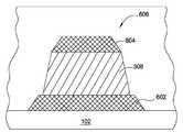
[0081]도 6a는, 디스플레이 디바이스들에서 활용되는 기판(102) 상에 형성될 수 있는 단순한 커패시터 구조(606)(예컨대, MIM(metal-insulating-metal) 구조)를 도시한다. 커패시터 구조(606)는 최상부 전극(604) 및 최하부 전극(602)을 포함하며, 이들 전극들 사이에, 복합 막 층(502)이 배치된다. 복합 막 층(502)은, 알루미늄 도핑된 ZrO2의 제1 층(510) 및 ZrO2의 제2 층(512)을 포함한다. 복합 막 층(502)은, 커패시터 구조(606)를 형성하기 위한, 전극들(604, 602) 사이의 커패시터 층으로서 기능하기 위해, 높은 유전 상수(예컨대, 유전 상수가 35 내지 50인 부분 및 15 내지 25인 부분)를 제공한다. 커패시터 구조(606)에서 커패시터 층으로서 기능하는 복합 막 층(502)은 또한, 필요에 따라, 임의의 개수의 층들의 형태일 수 있다. 대안적으로, 커패시터 구조(606)는, 도 6b에 도시된 바와 같은 커패시터 구조(606)를 형성하기 위해 사이에 배치되는 커패시터 층으로서, 도 3에서 위에 설명된 바와 같이, 높은 유전 상수 재료 층(308)을 가질 수 있다. 커패시터 층은, 알루미늄 도펀트들을 포함하는 ZrO2를 포함하는 하이-k(high-k) 재료를 포함한다. 커패시터 구조에서 커패시터 층으로서 기능하는 높은 유전 상수 재료 층(308)은 또한, 필요에 따라, 임의의 개수의 층들의 형태일 수 있다.6A shows a simple capacitor structure 606 (eg, a metal-insulating-metal (MIM) structure) that may be formed on a
[0082]도 7a는, 커패시터를 형성하기 위해 TFT 구조(750)에서 도 5a-5b의 복합 막 층(502) 또는 도 3a-3c의 높은 유전 상수 재료 층(308)을 활용하는 TFT 구조(750)의 예를 도시한다. 기판(102) 상에 형성되는 예시적인 TFT 디바이스 구조(750)의 일부분이 도 7a에 도시된다. TFT 디바이스 구조(750)는, OLED 디바이스에 대한 저온 폴리실리콘(LTPS; low temperature polysilicon) TFT를 포함한다. LTPS TFT 디바이스 구조(750)는, 상부에 배치된 선택적 절연 층(704)이 있는 또는 그러한 층이 없는 광학적으로 투명한 기판(102) 상에 형성된 소스 구역(709a), 채널 구역(708), 및 드레인 구역(709b)을 갖도록 만들어진 MOS 디바이스들이다. 일반적으로, 소스 구역(709a), 채널 구역(708), 및 드레인 구역(709b)은, 통상적으로 이후에 열 또는 레이저 프로세싱되어 폴리실리콘 층을 형성하는 초기에 증착된 비정질 실리콘(a-Si) 층으로부터 형성된다. 소스, 드레인, 및 채널 구역들(709a, 708, 709b)은, 광학적으로 투명한 기판(102) 상의 영역들을 패터닝하고 그리고 증착된 초기 a-Si 층(이후, 열적으로 프로세싱되거나 레이저 프로세싱(예컨대, 엑시머 레이저 어닐링(Excimer Laser Annealing) 프로세스)되어 폴리실리콘 층을 형성함)을 이온 도핑함으로써 형성될 수 있다. 이어서, 게이트 전극(714)을 채널 구역(708), 소스 구역(709a), 및 드레인 구역(709b)으로부터 격리시키기 위해, 게이트 절연 층(706)(예컨대, 도 2의 프로세스(200)에 의해 형성된 도 3a-3c의 높은 유전 상수 재료 층(308) 또는 도 4의 프로세스(400)에 의해 형성된 높은 유전 상수를 갖는 도 5a-5b의 복합 막 층(502) 또는 절연 층)이, 증착된 폴리실리콘 층(들)의 최상부 상에 증착될 수 있다. 게이트 전극(714)은 게이트 절연 층(706)의 최상부 상에 형성된다. 게이트 절연 층(706)은 또한 일반적으로 게이트 산화물 층으로 알려져 있다. 이어서, TFT 디바이스의 제어를 허용하기 위해, 커패시터 층(713)(예컨대, 이는 또한, 도 2의 프로세스(200)에 의해 형성된 도 3a-3c의 높은 유전 상수 재료 층(308) 또는 도 4의 프로세스(400)에 의해 형성된 높은 유전 상수를 갖는 도 5a-5b의 복합 막 층(502) 또는 절연 층일 수 있음) 및 디바이스 연결들이 절연 재료를 통해 만들어진다. 도 7a에 원들로 표시된 바와 같이, TFT 디바이스 구조(750)의 게이트 절연 층(706) 및 커패시터 층(713)은 또한, 상부에 형성된 제1 층(510) 및 제2 층(512)을 포함하는 높은 유전 상수뿐만 아니라 낮은 막 누설을 갖는 복합 막 층(502)에 의해, 또는 제1 층(304) 및 제2 층(306)을 포함하는 높은 유전 상수 재료 층(308)에 의해 제조될 수 있다.7A shows a
[0083]도 7a의 디바이스 구조(750)는, 디바이스 구조(750)에 게이트 절연 층(706) 또는 커패시터 층(713) 중 어느 하나 또는 둘 모두를 형성하는 데 활용되는, 디바이스 구조(750) 내의 일부 위치들에서 복합 막 층(502) 및 높은 유전 상수 재료 층(308)이 어느 위치에 활용될 수 있는지에 관한 설명 및 해설의 용이성을 위해 단지 부분적으로 형성되어 있다.[0083] The
[0084]커패시터 층(713)이 형성된 후에, 층간 절연체(730)가 커패시터 층(713) 상에 형성될 수 있다. 층간 절연체(730)는, 임의의 적절한 유전체 층, 이를테면, 실리콘 산화물 또는 실리콘 질화물 재료들일 수 있다. 층간 절연체(730)는, 커패시터 층(713) 상에 형성된 단일 층의 형태일 수 있다. 대안적으로, 층간 절연체(730)는, 상이한 디바이스 요건들에 따른 필요에 따라 다수의 층들의 형태일 수 있다. 도 7a에 도시된 예에서, 층간 절연체(730)는, 실리콘 산화물 층의 제2 유전체 층(734) 상에 형성된, 실리콘 질화물의 제1 유전체 층(732)을 포함한다. 후속하여, 소스 구역(709a) 및 드레인 구역들(709b)에 전기적으로 연결되도록, 이어서, 소스-드레인 금속 전극 층(710a, 710b)이 층간 절연체(730), 커패시터 층(713), 및 게이트 절연 층(706)에 증착, 형성, 및 패터닝된다.[0084] After the
[0085]소스-드레인 금속 전극 층(710a, 710b)이 패터닝된 후에, 이어서, 평탄화 층(735)이 소스-드레인 금속 전극 층(710a, 710b) 위에 형성된다. 평탄화 층(735)은, 폴리이미드, 벤조시클로부텐-시리즈 수지, SOG(spin on glass) 또는 아크릴레이트로 제조될 수 있다. 평탄화 층(735)은 이후, 소스-드레인 금속 전극 층(710a, 710b)에 전기적으로 연결되는 픽셀 전극(716)이 평탄화 층(735) 상에 형성되고 평탄화 층(735)에 충전되게 할 수 있도록 패터닝된다.[0085] After the source-drain
[0086]도 7a에 도시된 이러한 예에서, 상부 전극(710)과 하부 전극(707) 사이에 형성되는 커패시터 구조(712)(예컨대, MIM(metal-insulating-metal) 구조)로 연장되는 커패시터 층(713)이 게이트 전극(714) 상에 형성된다. 상부 전극(710)은 소스-드레인 금속 전극 층(710a, 710b)에 측방향으로 커플링될 수 있는 한편, 하부 전극(707)은, 게이트 전극(714) 또는 디바이스 구조(750) 내의 다른 적절한 전극들에 측방향으로 커플링될 수 있다. 디바이스 구조(750)에 형성된 커패시터 구조(712)는, 디스플레이 디바이스의 전기적 성능을 개선할 수 있는 저장 커패시터일 수 있다. 커패시터 구조(712)는, 상이한 디바이스 성능 요건들에 따른 필요에 따라 디바이스 구조(750)에서 적절한 임의의 위치에 형성될 수 있다는 것이 유의된다.[0086] In this example shown in FIG. 7A, a capacitor layer extending into a capacitor structure 712 (eg, a metal-insulating-metal (MIM) structure) formed between the
[0087]도 7b에 도시된 다른 예에서, 도 7a에 도시된 커패시터 구조(712)와 유사한 커패시터 구조(722)는, 상부 전극(710)과 하부 전극(707) 사이에 형성되는 커패시터 층(720)으로서 기능하는, 상이한 치수들 및/또는 프로파일들의 복합 막 층(502)으로 형성될 수 있다. 커패시터 층(713)이 게이트 전극(714) 위의 영역으로부터 상부 전극(710)과 하부 전극(707) 사이의 영역으로 연장되는 것과 달리, 도 7b에 도시된 커패시터 층(720)은, 실질적으로 상부 전극(710)과 하부 전극(707) 사이의 영역에 형성된다. 따라서, 커패시터 구조(722)를 둘러싸는, 실리콘 산화물을 포함하는 층간 절연체(724) 또는 실리콘 산화물이 게이트 절연 층(706) 상에 형성될 수 있다. 커패시터 층(720)으로서 커패시터 구조(722)에 형성되는 복합 막 층(502) 또는 높은 유전 상수 재료 층(308)은, 필요에 따라 하부 게이트 절연 층(706)과 접촉하는 최하부 표면을 가질 수 있다. 층간 절연체(724)는, 필요에 따라, 도 7b에 도시된 바와 같이 단일 층 형태일 수 있거나, 또는 다중 층 형태일 수 있다.[0087] In another example shown in FIG. 7B, a
[0088]프로세스(200 또는 300)에 의해 각각 형성되는 높은 유전 상수 재료 층(308) 또는 복합 막 층(502)은, 필요에 따라, 도 7b의 원들에 표시된 바와 같은 커패시터 층(720), 게이트 절연 층(706), 패시베이션 층, 또는 LCD에 대한 LTPS TFT 또는 OLED TFT를 포함하는 TFT 디바이스 구조들(750)의, 절연 재료들을 요구하는 임의의 다른 적절한 층들을 형성하는 데 활용될 수 있다는 것이 유의된다.[0088] The high dielectric
[0089]커패시터 구조들(722, 712)을 형성하는 데 활용되는 상부 전극(710) 및 하부 전극(707)은 또한, 필요에 따라, 픽셀 전극들 및/또는 공통 전극들일 수 있다는 것이 유의된다.It is noted that the
[0090]도 8은 TFT 디바이스 구조(850)의 또 다른 예를 도시한다. 위에 설명된 구조와 유사하게, 디바이스 구조(850)는, 게이트 전극(714) 상에 배치되는 레귤러(regular) 층간 절연체(820)를 포함한다. 패시베이션 층(822)이 층간 절연체(820) 상에 형성될 수 있다. (소스 및 드레인 구역(709a, 709b)에 전기적으로 연결되는) 소스 및 드레인 구역(802)의 다른 부분이 선택적 절연 층(704) 상에 도시된다. (소스-드레인 금속 전극 층(710a, 710b)에 전기적으로 연결되는) 소스-드레인 금속 전극 층(810)의 다른 부분이 소스 및 드레인 구역(802) 상에 배치되고 그리고 그에 전기적으로 커플링된다. 픽셀 전극(808)이 소스-드레인 금속 전극 층(810, 710a, 710b)에 전기적으로 연결될 수 있다. 이러한 특정 예에서, 게이트 절연 층(706)의 일부분이 게이트 전극(714)과 채널 구역(708) 사이를 통과하여 소스 및 드레인 구역(802) 위의 영역으로 연장된다. 일 예에서, 게이트 절연 층(706)은, 도 2의 프로세스(200)에 의해 형성된 도 3a-3c의 높은 유전 상수 재료 층(308), 또는 도 4를 참조하여 위에 설명된 프로세스(400)를 사용하여 형성된 제1 층(510) 및 제2 층(512)을 갖는 복합 막 층(502)일 수 있다. 디바이스 구조(850)의 커패시터 구조(806)를 형성하는 부가적인 전극(804)이 소스 및 드레인 구역(802) 및 게이트 절연 층(706) 위에 형성된다. 게이트 절연 층(706)(이제 또한 커패시터 층으로서 기능함) 상에 형성된 부가적인 전극(804)이 게이트 전극(714)에 전기적으로 연결될 수 있다. 따라서, 부가적인 전극(804) 및 소스 및 드레인 구역(802)은, 이들 사이에 형성된 게이트 절연 층(706)과 함께, 디바이스 구조(850)의 커패시터 구조(806)를 형성한다. 유사하게, 이제 또한 커패시터 층으로서 기능하는 게이트 절연 층(706)은, 필요에 따라, 층들 중 임의의 층의 형태일 수 있다.8 shows another example of a
[0091]소스-드레인 금속 전극 층(710a, 710b, 810), 픽셀 전극(808), 공통 전극, 게이트 전극(714), 상부 전극(710), 하부 전극(707), 최상부 전극(604), 최하부 전극(602), 부가적인 전극(804), 및 디바이스 구조들의 임의의 전극들은, 투명한 전도성 산화물 층(이를테면, ITO 등), 은 나노 잉크(silver nano ink), 탄소 나노 튜브(CNT), 은 나노 잉크 및 CNT, 그래핀, 알루미늄(Al), 텅스텐(W), 크롬(Cr), 탄탈룸(Ta), 몰리브덴(Mo), 구리(Cu), TiN, MoO2, MoNx, 이들의 결합 또는 다른 적절한 재료들을 포함하는 임의의 적절한 금속성 재료들일 수 있다는 것이 유의된다.[0091] Source-drain
[0092]도 8의 패시베이션 층(822) 위 또는 도 7a-7b의 평탄화 층(735) 위의 구조들은 간결성을 위해 제거되었다는 것이 유의된다. 그러나, 일부 예시적인 디바이스 구조들에서, 필요에 따라, 부가적인 OLED 또는 LCD 디바이스들, 또는 다른 적절한 디바이스들이 패시베이션 층(822) 또는 평탄화 층(735) 위에 형성되어, 다른 적절한 플렉서블 모바일 디스플레이 디바이스들, 이를테면, 터치 스크린 패널들을 갖는 LTPS OLED 디스플레이 디바이스들을 형성할 수 있다.[0092] It is noted that the structures above the
[0093]따라서, 본원에 설명된 방법들은, 원하는 높은 전기적 성능으로, 재료들(특히, ALD 또는 PE-ALD 프로세스에 의해 형성되는, 알루미늄 도펀트들을 갖는 ZrO2를 포함하는 하이-k 재료), 또는 (ALD 또는 PE-ALD 프로세스에 의해 형성되는, 알루미늄 도펀트들을 갖는 ZrO2를 포함하는 하이-k 재료의 제2 부분 및 ZrO2 층을 포함하는 하이-k 재료의 제1 부분을 갖는) 복합 막 층, 및 디스플레이 디바이스의 커패시터로서 형성되는 유전체 층과 함께, 디스플레이 디바이스들의 절연 재료들, 패시베이션 층, 층간 절연체, 커패시터 층, 게이트 절연 층의 구조들을 제어함으로써, 디스플레이 디바이스 구조들의 전자 안정성, 전기적 성능, 낮은 누설, 및 양호한 막 스택 통합을 유리하게 개선한다.[0093] Accordingly, the methods described herein are, with a desired high electrical performance, materials (especially a high-k material comprising ZrO2 with aluminum dopants, formed by an ALD or PE-ALD process), or A composite film layer (having a second portion of a high-k material comprising ZrO2 with aluminum dopants and a first portion of a high-k material comprising a ZrO2 layer, formed by an ALD or PE-ALD process) , And the dielectric layer formed as a capacitor of the display device, by controlling the structures of the insulating materials, passivation layer, interlayer insulator, capacitor layer, gate insulating layer of the display devices, the electronic stability, electrical performance, low It advantageously improves leakage, and good film stack integration.
[0094]전술한 내용들이 본 개시내용의 실시예들에 관한 것이지만, 본 개시내용의 다른 그리고 추가적인 실시예들이 본 개시내용의 기본적인 범위로부터 벗어나지 않으면서 안출될 수 있으며, 본 개시내용의 범위는 하기의 청구항들에 의해 결정된다.[0094] Although the foregoing contents relate to embodiments of the present disclosure, other and additional embodiments of the present disclosure may be devised without departing from the basic scope of the present disclosure, and the scope of the present disclosure is as follows. It is determined by the claims of.
Claims (15)
Translated fromKorean기판 상에 형성되는 유전체 층 ― 상기 유전체 층은, 알루미늄을 포함하는 지르코늄 함유 재료에 의해 형성되는 제1 층 및 결정질(crystalline) 지르코늄 함유 재료에 의해 형성되는 제2 층을 포함함 ―; 및
상기 기판 상에 형성되는 게이트 전극, 소스 전극, 및 드레인 전극을 포함하며,
상기 게이트 전극, 상기 소스 전극, 및 상기 드레인 전극은 상기 유전체 층 위 또는 아래에 형성되는, 박막 트랜지스터 구조.As a thin film transistor structure,
A dielectric layer formed on the substrate, the dielectric layer comprising a first layer formed by a zirconium-containing material comprising aluminum and a second layer formed by a crystalline zirconium-containing material; And
And a gate electrode, a source electrode, and a drain electrode formed on the substrate,
The gate electrode, the source electrode, and the drain electrode are formed above or below the dielectric layer.
상기 알루미늄을 포함하는 지르코늄 함유 재료로 이루어진 상기 제1 층은 비정질(amorphous) 구조를 갖는, 박막 트랜지스터 구조.The method of claim 1,
The first layer made of a zirconium-containing material including aluminum has an amorphous structure.
상기 제1 층은, 15 내지 25의 유전 상수를 갖는 알루미늄 도핑된 ZrO2 층인, 박막 트랜지스터 구조.The method of claim 1,
The first layer is an aluminum-doped ZrO2 layer having a dielectric constant of 15 to 25, a thin film transistor structure.
상기 제2 층은, 25 내지 50의 유전 상수를 갖는 ZrO2 층인, 박막 트랜지스터 구조.The method of claim 1,
The second layer is a ZrO2 layer having a dielectric constant of 25 to 50, the thin film transistor structure.
상기 게이트 전극 상에 형성되는 커패시터 층을 더 포함하며,
상기 커패시터 층은 알루미늄을 포함하는 지르코늄 함유 재료로 제조되거나, 또는 상기 커패시터 층은, 알루미늄을 포함하는 지르코늄 함유 재료로 제조되는 제1 부분 및 지르코늄 함유 재료로 제조되는 제2 부분을 갖는 복합 막 층인, 박막 트랜지스터 구조.The method of claim 1,
Further comprising a capacitor layer formed on the gate electrode,
The capacitor layer is made of a zirconium-containing material containing aluminum, or the capacitor layer is a composite film layer having a first portion made of a zirconium-containing material containing aluminum and a second portion made of a zirconium-containing material, Thin film transistor structure.
상기 유전체 층 또는 상기 커패시터 층은 원자 층 증착 프로세스에 의해 형성되는, 박막 트랜지스터 구조.The method of claim 7,
The dielectric layer or the capacitor layer is formed by an atomic layer deposition process.
상기 알루미늄을 포함하는 지르코늄 함유 재료는 비정질 구조를 갖거나; 또는
상기 알루미늄을 포함하는 지르코늄 함유 재료는 알루미늄 도핑된 ZrO2이거나; 또는
상기 알루미늄을 포함하는 지르코늄 함유 재료는 ALD 프로세스 또는 PE-ALD 프로세스에 의해 형성되거나; 또는
상기 알루미늄을 포함하는 지르코늄 함유 재료는 6 atm % 내지 20 atm %의 알루미늄 농도를 갖는, 박막 트랜지스터 구조.The method of claim 1,
The zirconium-containing material including aluminum has an amorphous structure; or
The zirconium-containing material containing aluminum is aluminum-doped ZrO2 ; or
The zirconium containing material comprising aluminum is formed by an ALD process or a PE-ALD process; or
The zirconium-containing material containing aluminum has an aluminum concentration of 6 atm% to 20 atm%, a thin film transistor structure.
투명 기판 상에 배치되는 제1 층 및 제2 층을 포함하는 복합 막 층을 형성하기 위해 ALD 프로세스를 수행하는 단계를 포함하며,
상기 제1 층은 상기 투명 기판 상에 형성되는 비정질 알루미늄 도핑된 지르코늄 함유 층을 포함하고 그리고 상기 제2 층은 결정질 지르코늄 함유 층을 포함하는, 디스플레이 디바이스들을 위한 복합 막 층을 형성하기 위한 방법.A method for forming a composite film layer for display devices, comprising:
Performing an ALD process to form a composite film layer comprising a first layer and a second layer disposed on a transparent substrate,
Wherein the first layer comprises an amorphous aluminum doped zirconium-containing layer formed on the transparent substrate and the second layer comprises a crystalline zirconium-containing layer.
상기 복합 막 층은, 디스플레이 디바이스의 커패시터 층 또는 게이트 절연 층으로서 활용되는, 디스플레이 디바이스들을 위한 복합 막 층을 형성하기 위한 방법.The method of claim 10,
The method for forming a composite film layer for display devices, wherein the composite film layer is utilized as a capacitor layer or a gate insulating layer of a display device.
상기 복합 막 층의 제1 층은, 상기 제1 층을 형성하기 위해 상기 기판에 알루미늄 함유 전구체 및 지르코늄 함유 전구체를 교번적으로(alternatively) 제공함으로써 형성되는, 디스플레이 디바이스들을 위한 복합 막 층을 형성하기 위한 방법.The method of claim 10,
The first layer of the composite film layer is formed by alternately providing an aluminum-containing precursor and a zirconium-containing precursor to the substrate to form the first layer to form a composite film layer for display devices. Way for you.
상기 알루미늄 함유 전구체 및 상기 지르코늄 함유 전구체와 함께, 또는 상기 알루미늄 함유 전구체 및 상기 지르코늄 함유 전구체의 각각의 펄스(pulse) 사이에, 산소 함유 가스를 제공하는 단계를 더 포함하는, 디스플레이 디바이스들을 위한 복합 막 층을 형성하기 위한 방법.The method of claim 12,
A composite film for display devices, further comprising providing an oxygen-containing gas with the aluminum-containing precursor and the zirconium-containing precursor, or between each pulse of the aluminum-containing precursor and the zirconium-containing precursor. Method for forming a layer.
상기 제1 층은 15 내지 25의 유전 상수를 갖는 알루미늄 도핑된 ZrO2 층이거나; 또는
상기 제2 층은 25 내지 50의 유전 상수를 갖는 ZrO2 층인, 디스플레이 디바이스들을 위한 복합 막 층을 형성하기 위한 방법.The method of claim 13,
The first layer is an aluminum doped ZrO2 layer having a dielectric constant of 15 to 25; or
Wherein thesecond layer is a ZrO2 layer having a dielectric constant of 25 to 50. A method for forming a composite film layer for display devices.
디스플레이 디바이스에서 2개의 전극들 사이에 형성되는 커패시터 층을 갖는 커패시터 구조를 포함하며, 상기 커패시터 층은, 15 내지 25의 유전 상수를 가진 비정질 구조를 갖는 알루미늄 도핑된 ZrO2 층 및 결정질 구조를 갖는 ZrO2 층을 포함하는, 디스플레이 디바이스에서 활용되는 디바이스 구조.As a device structure used in a display device,
A capacitor structure having a capacitor layer formed between two electrodes in a display device, the capacitor layer comprising an aluminum-doped ZrO2 layer having an amorphous structure having a dielectric constant of 15 to 25 and a ZrO having a crystalline structure A device structure utilized in a display device includingtwo layers.
Applications Claiming Priority (5)
| Application Number | Priority Date | Filing Date | Title |
|---|---|---|---|
| US201662364139P | 2016-07-19 | 2016-07-19 | |
| US201662364145P | 2016-07-19 | 2016-07-19 | |
| US62/364,139 | 2016-07-19 | ||
| US62/364,145 | 2016-07-19 | ||
| PCT/US2017/041555WO2018017360A2 (en) | 2016-07-19 | 2017-07-11 | High-k dielectric materials comprising zirconium oxide utilized in display devices |
Publications (2)
| Publication Number | Publication Date |
|---|---|
| KR20180125623A KR20180125623A (en) | 2018-11-23 |
| KR102208520B1true KR102208520B1 (en) | 2021-01-26 |
Family
ID=60992685
Family Applications (1)
| Application Number | Title | Priority Date | Filing Date |
|---|---|---|---|
| KR1020187033148AActiveKR102208520B1 (en) | 2016-07-19 | 2017-07-11 | High-k dielectric materials including zirconium oxide used in display devices |
Country Status (5)
| Country | Link |
|---|---|
| US (3) | US11239258B2 (en) |
| KR (1) | KR102208520B1 (en) |
| CN (1) | CN109075207B (en) |
| TW (4) | TWI808943B (en) |
| WO (1) | WO2018017360A2 (en) |
Families Citing this family (4)
| Publication number | Priority date | Publication date | Assignee | Title |
|---|---|---|---|---|
| KR102565412B1 (en)* | 2018-08-28 | 2023-08-10 | 삼성디스플레이 주식회사 | Organic light emitting display device |
| KR102727524B1 (en)* | 2018-12-04 | 2024-11-08 | 엘지디스플레이 주식회사 | Transistor, panel and manufactruing method for the transistor |
| KR102839363B1 (en)* | 2019-04-17 | 2025-07-29 | 에스케이하이닉스 주식회사 | Semiconductor device and method for manufacturing the same |
| US11335636B2 (en)* | 2019-10-29 | 2022-05-17 | Hefei Reliance Memory Limited | Gradual breakdown memory cell having multiple different dielectrics |
Citations (2)
| Publication number | Priority date | Publication date | Assignee | Title |
|---|---|---|---|---|
| KR100342316B1 (en)* | 1999-07-19 | 2002-07-02 | 마찌다 가쯔히꼬 | Aluminum-doped zirconium dielectric film transistor structure and deposition method same |
| JP2015230969A (en) | 2014-06-05 | 2015-12-21 | マイクロン テクノロジー, インク. | Semiconductor device and manufacturing method thereof |
Family Cites Families (64)
| Publication number | Priority date | Publication date | Assignee | Title |
|---|---|---|---|---|
| JPH11148078A (en) | 1997-11-18 | 1999-06-02 | Sanyo Electric Co Ltd | Active matrix type liquid crystal display device |
| US6713846B1 (en)* | 2001-01-26 | 2004-03-30 | Aviza Technology, Inc. | Multilayer high κ dielectric films |
| KR20020064624A (en) | 2001-02-02 | 2002-08-09 | 삼성전자 주식회사 | Dielectric layer for semiconductor device and method of fabricating the same |
| US7588989B2 (en) | 2001-02-02 | 2009-09-15 | Samsung Electronic Co., Ltd. | Dielectric multilayer structures of microelectronic devices and methods for fabricating the same |
| US6844604B2 (en)* | 2001-02-02 | 2005-01-18 | Samsung Electronics Co., Ltd. | Dielectric layer for semiconductor device and method of manufacturing the same |
| JP2002299632A (en) | 2001-03-30 | 2002-10-11 | Sanyo Electric Co Ltd | Semiconductor device and active matrix display device |
| US20020197823A1 (en) | 2001-05-18 | 2002-12-26 | Yoo Jae-Yoon | Isolation method for semiconductor device |
| JP2003069011A (en)* | 2001-08-27 | 2003-03-07 | Hitachi Ltd | Semiconductor device and manufacturing method thereof |
| US6514808B1 (en)* | 2001-11-30 | 2003-02-04 | Motorola, Inc. | Transistor having a high K dielectric and short gate length and method therefor |
| US6696332B2 (en)* | 2001-12-26 | 2004-02-24 | Texas Instruments Incorporated | Bilayer deposition to avoid unwanted interfacial reactions during high K gate dielectric processing |
| US6921702B2 (en)* | 2002-07-30 | 2005-07-26 | Micron Technology Inc. | Atomic layer deposited nanolaminates of HfO2/ZrO2 films as gate dielectrics |
| US6930059B2 (en)* | 2003-02-27 | 2005-08-16 | Sharp Laboratories Of America, Inc. | Method for depositing a nanolaminate film by atomic layer deposition |
| US7135369B2 (en)* | 2003-03-31 | 2006-11-14 | Micron Technology, Inc. | Atomic layer deposited ZrAlxOy dielectric layers including Zr4AlO9 |
| US7012027B2 (en)* | 2004-01-27 | 2006-03-14 | Taiwan Semiconductor Manufacturing Company, Ltd. | Zirconium oxide and hafnium oxide etching using halogen containing chemicals |
| KR100579194B1 (en) | 2004-05-28 | 2006-05-11 | 삼성에스디아이 주식회사 | Manufacturing method of organic electroluminescent display device |
| KR101133753B1 (en) | 2004-07-26 | 2012-04-09 | 삼성전자주식회사 | Liquid crystal display including sensing element |
| US20060125030A1 (en)* | 2004-12-13 | 2006-06-15 | Micron Technology, Inc. | Hybrid ALD-CVD of PrxOy/ZrO2 films as gate dielectrics |
| KR100700642B1 (en) | 2004-12-13 | 2007-03-27 | 삼성에스디아이 주식회사 | Organic light emitting display device and manufacturing method thereof |
| US7160781B2 (en)* | 2005-03-21 | 2007-01-09 | Infineon Technologies Ag | Transistor device and methods of manufacture thereof |
| KR100722989B1 (en)* | 2005-11-10 | 2007-05-30 | 주식회사 하이닉스반도체 | Capacitor and manufacturing method thereof |
| US7939396B2 (en)* | 2006-06-09 | 2011-05-10 | Taiwan Semiconductor Manufacturing Company, Ltd. | Base oxide engineering for high-K gate stacks |
| US7727908B2 (en)* | 2006-08-03 | 2010-06-01 | Micron Technology, Inc. | Deposition of ZrA1ON films |
| US7902018B2 (en)* | 2006-09-26 | 2011-03-08 | Applied Materials, Inc. | Fluorine plasma treatment of high-k gate stack for defect passivation |
| TWI316297B (en)* | 2006-11-10 | 2009-10-21 | Innolux Display Corp | Thin film transistor substrate |
| TWI323034B (en)* | 2006-12-25 | 2010-04-01 | Ind Tech Res Inst | Electronic devices with hybrid high-k dielectric and fabrication methods thereof |
| US20080182427A1 (en)* | 2007-01-26 | 2008-07-31 | Lars Oberbeck | Deposition method for transition-metal oxide based dielectric |
| JP2008203761A (en) | 2007-02-22 | 2008-09-04 | Hitachi Displays Ltd | Display device |
| WO2008108128A1 (en)* | 2007-03-08 | 2008-09-12 | Nec Corporation | Dielectric material, capacitor using dielectric material, semiconductor device using dielectric material, and method for producing dielectric material |
| US7763945B2 (en)* | 2007-04-18 | 2010-07-27 | Taiwan Semiconductor Manufacturing Co., Ltd. | Strained spacer design for protecting high-K gate dielectric |
| US7632745B2 (en)* | 2007-06-30 | 2009-12-15 | Intel Corporation | Hybrid high-k gate dielectric film |
| GB0720901D0 (en) | 2007-10-24 | 2007-12-05 | Shimadzu Res Lab Europe Ltd | Charged particle energy analysers |
| TWI380106B (en) | 2008-08-01 | 2012-12-21 | Chunghwa Picture Tubes Ltd | Pixel structure and method for repairing the same |
| DE102009004491A1 (en)* | 2009-01-09 | 2010-07-15 | Merck Patent Gmbh | Functional material for printed electronic components |
| KR100993416B1 (en)* | 2009-01-20 | 2010-11-09 | 삼성모바일디스플레이주식회사 | A flat panel display comprising a thin film transistor, a method of manufacturing the same, and a thin film transistor |
| TWI398710B (en)* | 2009-08-04 | 2013-06-11 | Au Optronics Corp | Pixel structure manufacturing method |
| US8115883B2 (en) | 2009-08-27 | 2012-02-14 | Semiconductor Energy Laboratory Co., Ltd. | Display device and method for manufacturing the same |
| US8779530B2 (en)* | 2009-12-21 | 2014-07-15 | Taiwan Semiconductor Manufacturing Company, Ltd. | Metal gate structure of a field effect transistor |
| KR101097333B1 (en) | 2010-02-11 | 2011-12-23 | 삼성모바일디스플레이주식회사 | Liquid Crystal Display Panel |
| JP5437895B2 (en) | 2010-04-20 | 2014-03-12 | 株式会社ジャパンディスプレイ | Display device and manufacturing method thereof |
| KR101710179B1 (en) | 2010-06-03 | 2017-02-27 | 삼성디스플레이 주식회사 | Flat panel display apparatus and manufacturing method of the same |
| JP5587716B2 (en)* | 2010-09-27 | 2014-09-10 | マイクロンメモリジャパン株式会社 | Semiconductor device, manufacturing method thereof, and adsorption site blocking atomic layer deposition method |
| KR101824537B1 (en) | 2010-10-01 | 2018-03-15 | 삼성디스플레이 주식회사 | Thin film transistor and organic light emitting display |
| KR20120061312A (en) | 2010-12-03 | 2012-06-13 | 삼성모바일디스플레이주식회사 | Organic light emitting display device and method of manufacturing the same |
| US20120235276A1 (en)* | 2011-03-18 | 2012-09-20 | Intermolecular, Inc. | Electrode treatments for enhanced dram performance |
| KR20120124527A (en) | 2011-05-04 | 2012-11-14 | 삼성디스플레이 주식회사 | Display device and method of manufacturing a display device |
| TWI423310B (en) | 2011-06-10 | 2014-01-11 | Au Optronics Corp | Pixel structure |
| US8415227B2 (en)* | 2011-08-29 | 2013-04-09 | Intermolecular, Inc. | High performance dielectric stack for DRAM capacitor |
| KR101884824B1 (en)* | 2011-09-07 | 2018-08-03 | 삼성디스플레이 주식회사 | Thin film transistor and manufacturing method thereof |
| KR102025836B1 (en) | 2011-11-07 | 2019-09-27 | 삼성디스플레이 주식회사 | Thin-film transistor array substrate, organic light emitting display device comprising the same and method for manufacturing of the thin-film transistor array substrate |
| KR101945237B1 (en) | 2012-06-01 | 2019-02-08 | 삼성디스플레이 주식회사 | Organic light emitting diode display |
| US8741712B2 (en)* | 2012-09-18 | 2014-06-03 | Intermolecular, Inc. | Leakage reduction in DRAM MIM capacitors |
| US8815695B2 (en)* | 2012-12-27 | 2014-08-26 | Intermolecular, Inc. | Methods to improve leakage for ZrO2 based high K MIM capacitor |
| KR20150021622A (en) | 2013-08-20 | 2015-03-03 | 삼성디스플레이 주식회사 | Display panel |
| KR102169014B1 (en)* | 2013-10-14 | 2020-10-23 | 삼성디스플레이 주식회사 | Thin film transistor array substrate and manufacturing method for the same |
| US9331168B2 (en)* | 2014-01-17 | 2016-05-03 | Taiwan Semiconductor Manufacturing Company Ltd. | Semiconductor structure and manufacuturing method of the same |
| TWI551926B (en) | 2014-01-27 | 2016-10-01 | 友達光電股份有限公司 | Pixel structure |
| JP6545976B2 (en)* | 2014-03-07 | 2019-07-17 | 株式会社半導体エネルギー研究所 | Semiconductor device |
| CN103972110B (en)* | 2014-04-22 | 2016-02-24 | 京东方科技集团股份有限公司 | Thin-film transistor and preparation method thereof, array base palte, display unit |
| KR102760229B1 (en)* | 2014-05-30 | 2025-02-03 | 가부시키가이샤 한도오따이 에네루기 켄큐쇼 | Semiconductor device, manufacturing method thereof, and electronic device |
| US9634145B2 (en)* | 2014-10-29 | 2017-04-25 | Eastman Kodak Company | TFT substrate with variable dielectric thickness |
| US9466661B2 (en)* | 2014-10-10 | 2016-10-11 | Globalfoundries Inc. | Method of fabricating a MIM capacitor with minimal voltage coefficient and a decoupling MIM capacitor and analog/RF MIM capacitor on the same chip with high-K dielectrics |
| US10147823B2 (en)* | 2015-03-19 | 2018-12-04 | Semiconductor Energy Laboratory Co., Ltd. | Semiconductor device |
| US10103269B2 (en)* | 2015-05-08 | 2018-10-16 | Lg Chem, Ltd. | Thin-film transistor substrate having a light reflection reduction layer and display device comprising same |
| JP7142081B2 (en)* | 2018-03-06 | 2022-09-26 | 株式会社半導体エネルギー研究所 | Laminate and semiconductor device |
- 2017
- 2017-07-11KRKR1020187033148Apatent/KR102208520B1/enactiveActive
- 2017-07-11WOPCT/US2017/041555patent/WO2018017360A2/ennot_activeCeased
- 2017-07-11USUS15/773,640patent/US11239258B2/enactiveActive
- 2017-07-11CNCN201780026052.8Apatent/CN109075207B/enactiveActive
- 2017-07-12TWTW106123346Apatent/TWI808943B/enactive
- 2017-07-12TWTW113109455Apatent/TWI869233B/enactive
- 2017-07-12TWTW112122940Apatent/TWI840259B/enactive
- 2017-07-12TWTW113146070Apatent/TWI890629B/enactive
- 2022
- 2022-01-07USUS17/647,404patent/US11894396B2/enactiveActive
- 2023
- 2023-12-19USUS18/545,810patent/US12148766B2/enactiveActive
Patent Citations (2)
| Publication number | Priority date | Publication date | Assignee | Title |
|---|---|---|---|---|
| KR100342316B1 (en)* | 1999-07-19 | 2002-07-02 | 마찌다 가쯔히꼬 | Aluminum-doped zirconium dielectric film transistor structure and deposition method same |
| JP2015230969A (en) | 2014-06-05 | 2015-12-21 | マイクロン テクノロジー, インク. | Semiconductor device and manufacturing method thereof |
Also Published As
| Publication number | Publication date |
|---|---|
| US11239258B2 (en) | 2022-02-01 |
| TWI840259B (en) | 2024-04-21 |
| US12148766B2 (en) | 2024-11-19 |
| TWI869233B (en) | 2025-01-01 |
| TW201813089A (en) | 2018-04-01 |
| US20240120349A1 (en) | 2024-04-11 |
| TW202427793A (en) | 2024-07-01 |
| US11894396B2 (en) | 2024-02-06 |
| TWI808943B (en) | 2023-07-21 |
| WO2018017360A2 (en) | 2018-01-25 |
| CN109075207B (en) | 2023-08-11 |
| US20200258918A1 (en) | 2020-08-13 |
| WO2018017360A3 (en) | 2018-07-26 |
| TW202339264A (en) | 2023-10-01 |
| US20220130873A1 (en) | 2022-04-28 |
| CN109075207A (en) | 2018-12-21 |
| KR20180125623A (en) | 2018-11-23 |
| TWI890629B (en) | 2025-07-11 |
Similar Documents
| Publication | Publication Date | Title |
|---|---|---|
| US12148766B2 (en) | High-K dielectric materials comprising zirconium oxide utilized in display devices | |
| US12080725B2 (en) | Hybrid high-K dielectric material film stacks comprising zirconium oxide utilized in display devices | |
| US11600642B2 (en) | Layer stack for display applications | |
| TW202531903A (en) | Device structure and method for forming composite film layer for display devices |
Legal Events
| Date | Code | Title | Description |
|---|---|---|---|
| A201 | Request for examination | ||
| PA0105 | International application | Patent event date:20181115 Patent event code:PA01051R01D Comment text:International Patent Application | |
| PA0201 | Request for examination | ||
| PG1501 | Laying open of application | ||
| E902 | Notification of reason for refusal | ||
| PE0902 | Notice of grounds for rejection | Comment text:Notification of reason for refusal Patent event date:20200214 Patent event code:PE09021S01D | |
| E701 | Decision to grant or registration of patent right | ||
| PE0701 | Decision of registration | Patent event code:PE07011S01D Comment text:Decision to Grant Registration Patent event date:20201028 | |
| GRNT | Written decision to grant | ||
| PR0701 | Registration of establishment | Comment text:Registration of Establishment Patent event date:20210121 Patent event code:PR07011E01D | |
| PR1002 | Payment of registration fee | Payment date:20210121 End annual number:3 Start annual number:1 | |
| PG1601 | Publication of registration | ||
| PR1001 | Payment of annual fee | Payment date:20231227 Start annual number:4 End annual number:4 | |
| PR1001 | Payment of annual fee | Payment date:20241224 Start annual number:5 End annual number:5 |