KR102207992B1 - 서브-포화된 원자층 증착 및 등각막 증착 - Google Patents
서브-포화된 원자층 증착 및 등각막 증착Download PDFInfo
- Publication number
- KR102207992B1 KR102207992B1KR1020130126834AKR20130126834AKR102207992B1KR 102207992 B1KR102207992 B1KR 102207992B1KR 1020130126834 AKR1020130126834 AKR 1020130126834AKR 20130126834 AKR20130126834 AKR 20130126834AKR 102207992 B1KR102207992 B1KR 102207992B1
- Authority
- KR
- South Korea
- Prior art keywords
- reactant
- dose
- film
- plasma
- substrate surface
- Prior art date
- Legal status (The legal status is an assumption and is not a legal conclusion. Google has not performed a legal analysis and makes no representation as to the accuracy of the status listed.)
- Active
Links
Images


Classifications
- C—CHEMISTRY; METALLURGY
- C23—COATING METALLIC MATERIAL; COATING MATERIAL WITH METALLIC MATERIAL; CHEMICAL SURFACE TREATMENT; DIFFUSION TREATMENT OF METALLIC MATERIAL; COATING BY VACUUM EVAPORATION, BY SPUTTERING, BY ION IMPLANTATION OR BY CHEMICAL VAPOUR DEPOSITION, IN GENERAL; INHIBITING CORROSION OF METALLIC MATERIAL OR INCRUSTATION IN GENERAL
- C23C—COATING METALLIC MATERIAL; COATING MATERIAL WITH METALLIC MATERIAL; SURFACE TREATMENT OF METALLIC MATERIAL BY DIFFUSION INTO THE SURFACE, BY CHEMICAL CONVERSION OR SUBSTITUTION; COATING BY VACUUM EVAPORATION, BY SPUTTERING, BY ION IMPLANTATION OR BY CHEMICAL VAPOUR DEPOSITION, IN GENERAL
- C23C16/00—Chemical coating by decomposition of gaseous compounds, without leaving reaction products of surface material in the coating, i.e. chemical vapour deposition [CVD] processes
- C23C16/44—Chemical coating by decomposition of gaseous compounds, without leaving reaction products of surface material in the coating, i.e. chemical vapour deposition [CVD] processes characterised by the method of coating
- C23C16/455—Chemical coating by decomposition of gaseous compounds, without leaving reaction products of surface material in the coating, i.e. chemical vapour deposition [CVD] processes characterised by the method of coating characterised by the method used for introducing gases into reaction chamber or for modifying gas flows in reaction chamber
- C23C16/45523—Pulsed gas flow or change of composition over time
- C23C16/45525—Atomic layer deposition [ALD]
- C23C16/45527—Atomic layer deposition [ALD] characterized by the ALD cycle, e.g. different flows or temperatures during half-reactions, unusual pulsing sequence, use of precursor mixtures or auxiliary reactants or activations
- C23C16/45536—Use of plasma, radiation or electromagnetic fields
- C23C16/4554—Plasma being used non-continuously in between ALD reactions
- H—ELECTRICITY
- H01—ELECTRIC ELEMENTS
- H01L—SEMICONDUCTOR DEVICES NOT COVERED BY CLASS H10
- H01L21/00—Processes or apparatus adapted for the manufacture or treatment of semiconductor or solid state devices or of parts thereof
- H01L21/02—Manufacture or treatment of semiconductor devices or of parts thereof
- H01L21/02104—Forming layers
- H01L21/02107—Forming insulating materials on a substrate
- H01L21/02109—Forming insulating materials on a substrate characterised by the type of layer, e.g. type of material, porous/non-porous, pre-cursors, mixtures or laminates
- H01L21/02112—Forming insulating materials on a substrate characterised by the type of layer, e.g. type of material, porous/non-porous, pre-cursors, mixtures or laminates characterised by the material of the layer
- H01L21/02123—Forming insulating materials on a substrate characterised by the type of layer, e.g. type of material, porous/non-porous, pre-cursors, mixtures or laminates characterised by the material of the layer the material containing silicon
- H01L21/02164—Forming insulating materials on a substrate characterised by the type of layer, e.g. type of material, porous/non-porous, pre-cursors, mixtures or laminates characterised by the material of the layer the material containing silicon the material being a silicon oxide, e.g. SiO2
- H—ELECTRICITY
- H01—ELECTRIC ELEMENTS
- H01L—SEMICONDUCTOR DEVICES NOT COVERED BY CLASS H10
- H01L21/00—Processes or apparatus adapted for the manufacture or treatment of semiconductor or solid state devices or of parts thereof
- H01L21/02—Manufacture or treatment of semiconductor devices or of parts thereof
- H01L21/02104—Forming layers
- H01L21/02107—Forming insulating materials on a substrate
- H01L21/02109—Forming insulating materials on a substrate characterised by the type of layer, e.g. type of material, porous/non-porous, pre-cursors, mixtures or laminates
- H01L21/02205—Forming insulating materials on a substrate characterised by the type of layer, e.g. type of material, porous/non-porous, pre-cursors, mixtures or laminates the layer being characterised by the precursor material for deposition
- H01L21/02208—Forming insulating materials on a substrate characterised by the type of layer, e.g. type of material, porous/non-porous, pre-cursors, mixtures or laminates the layer being characterised by the precursor material for deposition the precursor containing a compound comprising Si
- H01L21/02219—Forming insulating materials on a substrate characterised by the type of layer, e.g. type of material, porous/non-porous, pre-cursors, mixtures or laminates the layer being characterised by the precursor material for deposition the precursor containing a compound comprising Si the compound comprising silicon and nitrogen
- H—ELECTRICITY
- H01—ELECTRIC ELEMENTS
- H01L—SEMICONDUCTOR DEVICES NOT COVERED BY CLASS H10
- H01L21/00—Processes or apparatus adapted for the manufacture or treatment of semiconductor or solid state devices or of parts thereof
- H01L21/02—Manufacture or treatment of semiconductor devices or of parts thereof
- H01L21/02104—Forming layers
- H01L21/02107—Forming insulating materials on a substrate
- H01L21/02225—Forming insulating materials on a substrate characterised by the process for the formation of the insulating layer
- H01L21/0226—Forming insulating materials on a substrate characterised by the process for the formation of the insulating layer formation by a deposition process
- H01L21/02263—Forming insulating materials on a substrate characterised by the process for the formation of the insulating layer formation by a deposition process deposition from the gas or vapour phase
- H01L21/02271—Forming insulating materials on a substrate characterised by the process for the formation of the insulating layer formation by a deposition process deposition from the gas or vapour phase deposition by decomposition or reaction of gaseous or vapour phase compounds, i.e. chemical vapour deposition
- H01L21/02274—Forming insulating materials on a substrate characterised by the process for the formation of the insulating layer formation by a deposition process deposition from the gas or vapour phase deposition by decomposition or reaction of gaseous or vapour phase compounds, i.e. chemical vapour deposition in the presence of a plasma [PECVD]
- H—ELECTRICITY
- H01—ELECTRIC ELEMENTS
- H01L—SEMICONDUCTOR DEVICES NOT COVERED BY CLASS H10
- H01L21/00—Processes or apparatus adapted for the manufacture or treatment of semiconductor or solid state devices or of parts thereof
- H01L21/02—Manufacture or treatment of semiconductor devices or of parts thereof
- H01L21/02104—Forming layers
- H01L21/02107—Forming insulating materials on a substrate
- H01L21/02225—Forming insulating materials on a substrate characterised by the process for the formation of the insulating layer
- H01L21/0226—Forming insulating materials on a substrate characterised by the process for the formation of the insulating layer formation by a deposition process
- H01L21/02263—Forming insulating materials on a substrate characterised by the process for the formation of the insulating layer formation by a deposition process deposition from the gas or vapour phase
- H01L21/02271—Forming insulating materials on a substrate characterised by the process for the formation of the insulating layer formation by a deposition process deposition from the gas or vapour phase deposition by decomposition or reaction of gaseous or vapour phase compounds, i.e. chemical vapour deposition
- H01L21/0228—Forming insulating materials on a substrate characterised by the process for the formation of the insulating layer formation by a deposition process deposition from the gas or vapour phase deposition by decomposition or reaction of gaseous or vapour phase compounds, i.e. chemical vapour deposition deposition by cyclic CVD, e.g. ALD, ALE, pulsed CVD
- H—ELECTRICITY
- H01—ELECTRIC ELEMENTS
- H01L—SEMICONDUCTOR DEVICES NOT COVERED BY CLASS H10
- H01L21/00—Processes or apparatus adapted for the manufacture or treatment of semiconductor or solid state devices or of parts thereof
- H01L21/02—Manufacture or treatment of semiconductor devices or of parts thereof
- H01L21/04—Manufacture or treatment of semiconductor devices or of parts thereof the devices having potential barriers, e.g. a PN junction, depletion layer or carrier concentration layer
- H01L21/18—Manufacture or treatment of semiconductor devices or of parts thereof the devices having potential barriers, e.g. a PN junction, depletion layer or carrier concentration layer the devices having semiconductor bodies comprising elements of Group IV of the Periodic Table or AIIIBV compounds with or without impurities, e.g. doping materials
- H01L21/30—Treatment of semiconductor bodies using processes or apparatus not provided for in groups H01L21/20 - H01L21/26
- H01L21/31—Treatment of semiconductor bodies using processes or apparatus not provided for in groups H01L21/20 - H01L21/26 to form insulating layers thereon, e.g. for masking or by using photolithographic techniques; After treatment of these layers; Selection of materials for these layers
- H01L21/3105—After-treatment
- H01L21/311—Etching the insulating layers by chemical or physical means
- H01L21/31105—Etching inorganic layers
- H01L21/31111—Etching inorganic layers by chemical means
Landscapes
- Engineering & Computer Science (AREA)
- Chemical & Material Sciences (AREA)
- Physics & Mathematics (AREA)
- Chemical Kinetics & Catalysis (AREA)
- General Physics & Mathematics (AREA)
- Computer Hardware Design (AREA)
- Power Engineering (AREA)
- Microelectronics & Electronic Packaging (AREA)
- Manufacturing & Machinery (AREA)
- Condensed Matter Physics & Semiconductors (AREA)
- General Chemical & Material Sciences (AREA)
- Materials Engineering (AREA)
- Mechanical Engineering (AREA)
- Organic Chemistry (AREA)
- Metallurgy (AREA)
- Plasma & Fusion (AREA)
- Electromagnetism (AREA)
- Chemical Vapour Deposition (AREA)
- Formation Of Insulating Films (AREA)
Abstract
Description
도 2는 기재된 실시형태들에 따른, 다른 예시적인 플라즈마-활성화된 SS-ALD 프로세스에 대한 타이밍도를 개략적으로 도시한다.
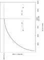
도 3a는 다양한 실시형태들에 따른 도즈 포화 곡선의 일 예를 도시한다.
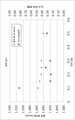
도 3b는 다양한 도즈 시간들을 사용하여 증착된 실리콘 산화물 막들의 비균일도 및 증착 레이트에 관련된 데이터를 도시한다.
도 4a는 다양한 도즈 시간들을 사용하여 증착된 실리콘 산화물 막들의 비균일도 및 증착 레이트에 관련된 데이터를 도시한다.
도 4b는 다양한 온도들에서 증착되는 실리콘 산화물 막들의 습식 에칭 속성들에 관련된 데이터를 도시한다.
도 4c는 400℃에서 증착된 막들에 대한 변환 효율도 및 습식 에칭 레이트에 관련된 데이터를 도시한다.
도 4d는 200℃에서 증착된 막들에 대한 변환 효율도 및 습식 에칭 레이트에 관련된 데이터를 도시한다.
도 4e는 압력을 변화시키면서, 50℃에서 증착된 막들에 대한 높은 무선 주파수 에너지 및 열적 산화물에 대한 습식 에칭 레이트 비율들에 관련된 데이터를 도시한다.
도 4f는 시간들에 따른 다양한 RF 플라즈마를 사용하는 증착 레이트 및 비균일도에 관련된 데이터를 도시한다.
도 4g는 다양한 사후-도즈 퍼지 시간들을 사용하는 증착 레이트 및 비균일도에 관련된 데이터를 도시한다.
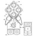
도 5는 본 발명의 일 실시형태에 따른 복수의 프로세스 스테이션들 및 제어기를 포함하는 예시적인 프로세스 툴을 개략적으로 도시한다.
도 6은 본 발명의 일 실시형태에 따른 예시적인 프로세스 스테이션을 개략적으로 도시한다.


Claims (22)
- 기판 표면 상에 막을 증착시키기 위한 방법으로서,
반응 챔버에 토포그래픽 (topographical) 피쳐들을 포함하는 기판을 제공하는 단계;
제 1 반응물이 상기 기판 표면 상으로 흡착되게 하는 조건들 하에서 상기 반응 챔버에 증기 페이즈 (vapor phase) 로 상기 제 1 반응물을 도입하는 단계;
도즈 시간 (dose time) 동안 상기 반응 챔버에 증기 페이즈로 제 2 반응물의 도즈를 도입하는 단계로서, 상기 제 2 반응물의 도즈는 서브-포화된 (sub-saturated) 도즈인, 상기 제 2 반응물의 도즈를 도입하는 단계; 및
막이 상기 토포그래픽 피쳐들과 일치하도록 (conform) 상기 막을 형성하기 위해 상기 제 2 반응물의 도즈가 상기 기판 표면 상의 상기 제 1 반응물과 상기 제 2 반응물 사이에서 표면 반응을 일으키게 하기 위해 중지된 경우, 상기 기판 표면을 플라즈마에 주기적으로 노출시키는 단계를 포함하는, 기판 표면 상에 막을 증착시키기 위한 방법. - 제 1 항에 있어서,
상기 반응물들 중 적어도 하나가 가스 페이즈에 있으면서 상기 플라즈마가 점화되는, 기판 표면 상에 막을 증착시키기 위한 방법. - 제 1 항에 있어서,
증착 온도는 200℃ 미만인, 기판 표면 상에 막을 증착시키기 위한 방법. - 제 1 항에 있어서,
증착 온도는 150℃ 미만인, 기판 표면 상에 막을 증착시키기 위한 방법. - 제 1 항에 있어서,
플라즈마 노출은 적어도 50J/mL의 변환 효율도를 가지며,
상기 변환 효율도는 상기 서브-포화된 도즈에서 제 2 반응물 플럭스의 단위 당 적용된 플라즈마 에너지의 양인, 기판 표면 상에 막을 증착시키기 위한 방법. - 제 1 항에 있어서,
플라즈마 노출은 적어도 150J/mL의 변환 효율도를 가지며,
상기 변환 효율도는 상기 서브-포화된 도즈에서 제 2 반응물 플럭스의 단위 당 적용된 플라즈마 에너지의 양인, 기판 표면 상에 막을 증착시키기 위한 방법. - 제 1 항에 있어서,
상기 제 1 반응물은 산화제인, 기판 표면 상에 막을 증착시키기 위한 방법. - 제 1 항에 있어서,
상기 제 2 반응물의 도즈를 도입하기 전에, 도즈 포화 곡선을 통해 상기 제 2 반응물의 포화된 도즈를 결정하는 단계를 더 포함하는, 기판 표면 상에 막을 증착시키기 위한 방법. - 제 1 항에 있어서,
상기 서브-포화된 도즈는 상기 제 2 반응물의 4마이크로리터 미만인, 기판 표면 상에 막을 증착시키기 위한 방법. - 제 1 항에 있어서,
상기 서브-포화된 도즈는 포화된 도즈의 60% 미만인, 기판 표면 상에 막을 증착시키기 위한 방법. - 제 1 항에 있어서,
상기 기판을 플라즈마에 노출시키기 전에, 퍼지 시간 (purge time) 동안 증기 페이즈로 잔류 제 2 반응물을 퍼지 아웃 (purge out) 시키는 단계를 더 포함하며,
서브-포화된 도즈 시간 대 상기 퍼지 시간의 비율은 2 미만인, 기판 표면 상에 막을 증착시키기 위한 방법. - 제 1 항 내지 제 11 항 중 어느 한 항에 있어서,
상기 제 2 반응물은 적어도 50Da의 분자량의 둘러싼 원자를 갖는 전구체 분자인, 기판 표면 상에 막을 증착시키기 위한 방법. - 제 1 항 내지 제 11 항 중 어느 한 항에 있어서,
상기 제 2 반응물은 적어도 140Da의 분자량의 둘러싼 원자를 갖는 전구체 분자인, 기판 표면 상에 막을 증착시키기 위한 방법. - 제 1 항 내지 제 11 항 중 어느 한 항에 있어서,
증착된 상기 막은 두께가 0.5Å 미만인, 기판 표면 상에 막을 증착시키기 위한 방법. - 제 1 항 내지 제 11 항 중 어느 한 항에 있어서,
증착된 상기 막은 두께가 0.1Å 미만인, 기판 표면 상에 막을 증착시키기 위한 방법. - 제 1 항에 있어서,
상기 막은 1.0% 미만의 웨이퍼 내 비-균일도를 갖는, 기판 표면 상에 막을 증착시키기 위한 방법. - 기판 표면 상에 막을 증착시키기 위한 방법으로서,
단일의 스테이션 또는 멀티-스테이션 반응 챔버의 스테이션에 토포그래픽 피쳐들을 포함하는 기판을 제공하는 단계;
제 1 반응물이 상기 기판 표면 상으로 흡착되게 하는 조건들 하에서 상기 챔버에 증기 페이즈로 상기 제 1 반응물을 도입하는 단계;
상기 반응 챔버에 증기 페이즈로 제 2 반응물의 도즈를 도입하는 단계로서, 상기 제 2 반응물의 도즈는 서브-포화된 도즈인, 상기 제 2 반응물의 도즈를 도입하는 단계; 및
막이 상기 토포그래픽 피쳐들과 일치하도록 상기 막을 형성하기 위해 상기 제 2 반응물의 도즈가 상기 기판 표면 상의 상기 제 1 반응물과 상기 제 2 반응물 사이에서 표면 반응을 일으키게 하기 위해 중지된 경우, 상기 기판 표면을 플라즈마에 주기적으로 노출시키는 단계를 포함하며,
상기 플라즈마는 챔버 당 적어도 200줄 (Joule) 의 에너지로 생성되는, 기판 표면 상에 막을 증착시키기 위한 방법. - 제 17 항에 있어서,
증착 온도는 150℃ 미만인, 기판 표면 상에 막을 증착시키기 위한 방법. - 제 17 항에 있어서,
상기 제 2 반응물의 도즈를 도입하기 전에, 도즈 포화 곡선을 통해 상기 제 2 반응물의 도즈를 결정하는 단계를 더 포함하는, 기판 표면 상에 막을 증착시키기 위한 방법. - 제 17 항에 있어서,
플라즈마 노출은 적어도 50J/mL의 변환 효율도를 갖는, 기판 표면 상에 막을 증착시키기 위한 방법. - 제 17 항 내지 제 20 항 중 어느 한 항에 있어서,
증착된 상기 막은 두께가 0.1Å 미만인, 기판 표면 상에 막을 증착시키기 위한 방법. - 기판 상에 막들을 증착시키기 위한 장치로서,
반응 챔버;
상기 반응 챔버에 가스 페이즈 반응물들을 전달하기 위한 입구 포트;
상기 반응 챔버에 플라즈마를 제공하기 위한 플라즈마 생성기; 및
제어기를 포함하고,
상기 제어기는,
제 1 반응물이 기판 표면 상으로 흡착되게 하는 조건들 하에서 상기 반응 챔버에 증기 페이즈로 상기 제 1 반응물을 흐르게 하기 위한 명령들;
도즈 시간 동안 상기 반응 챔버에 증기 페이즈로 제 2 반응물의 도즈를 흐르게 하기 위한 명령들로서, 상기 제 2 반응물의 도즈는 서브-포화된 도즈인, 상기 제 2 반응물의 도즈를 흐르게 하기 위한 명령들; 및
막이 토포그래픽 피쳐들과 일치하도록 상기 막을 형성하기 위해 상기 제 2 반응물의 도즈가 상기 기판 표면 상의 상기 제 1 반응물과 상기 제 2 반응물 사이에서 표면 반응을 일으키게 하기 위해 중지될 경우, 적어도 50J/mL의 변환 효율도로 상기 반응 챔버에 플라즈마를 주기적으로 공급하기 위한 명령들을 포함하고,
상기 변환 효율도는 상기 서브-포화된 도즈에서 제 2 반응물 플럭스의 단위 당 적용된 플라즈마 에너지의 양인, 기판 상에 막들을 증착시키기 위한 장치.
Priority Applications (1)
| Application Number | Priority Date | Filing Date | Title |
|---|---|---|---|
| KR1020210008342AKR102328850B1 (ko) | 2012-10-23 | 2021-01-20 | 서브-포화된 원자층 증착 및 등각막 증착 |
Applications Claiming Priority (2)
| Application Number | Priority Date | Filing Date | Title |
|---|---|---|---|
| US201261717576P | 2012-10-23 | 2012-10-23 | |
| US61/717,576 | 2012-10-23 |
Related Child Applications (1)
| Application Number | Title | Priority Date | Filing Date |
|---|---|---|---|
| KR1020210008342ADivisionKR102328850B1 (ko) | 2012-10-23 | 2021-01-20 | 서브-포화된 원자층 증착 및 등각막 증착 |
Publications (2)
| Publication Number | Publication Date |
|---|---|
| KR20140051807A KR20140051807A (ko) | 2014-05-02 |
| KR102207992B1true KR102207992B1 (ko) | 2021-01-26 |
Family
ID=50547644
Family Applications (2)
| Application Number | Title | Priority Date | Filing Date |
|---|---|---|---|
| KR1020130126834AActiveKR102207992B1 (ko) | 2012-10-23 | 2013-10-23 | 서브-포화된 원자층 증착 및 등각막 증착 |
| KR1020210008342AActiveKR102328850B1 (ko) | 2012-10-23 | 2021-01-20 | 서브-포화된 원자층 증착 및 등각막 증착 |
Family Applications After (1)
| Application Number | Title | Priority Date | Filing Date |
|---|---|---|---|
| KR1020210008342AActiveKR102328850B1 (ko) | 2012-10-23 | 2021-01-20 | 서브-포화된 원자층 증착 및 등각막 증착 |
Country Status (3)
| Country | Link |
|---|---|
| US (1) | US9355839B2 (ko) |
| KR (2) | KR102207992B1 (ko) |
| TW (1) | TWI595112B (ko) |
Families Citing this family (88)
| Publication number | Priority date | Publication date | Assignee | Title |
|---|---|---|---|---|
| US20110256734A1 (en) | 2010-04-15 | 2011-10-20 | Hausmann Dennis M | Silicon nitride films and methods |
| US9892917B2 (en) | 2010-04-15 | 2018-02-13 | Lam Research Corporation | Plasma assisted atomic layer deposition of multi-layer films for patterning applications |
| US8956983B2 (en) | 2010-04-15 | 2015-02-17 | Novellus Systems, Inc. | Conformal doping via plasma activated atomic layer deposition and conformal film deposition |
| US9611544B2 (en) | 2010-04-15 | 2017-04-04 | Novellus Systems, Inc. | Plasma activated conformal dielectric film deposition |
| US9997357B2 (en) | 2010-04-15 | 2018-06-12 | Lam Research Corporation | Capped ALD films for doping fin-shaped channel regions of 3-D IC transistors |
| US9257274B2 (en) | 2010-04-15 | 2016-02-09 | Lam Research Corporation | Gapfill of variable aspect ratio features with a composite PEALD and PECVD method |
| US9076646B2 (en) | 2010-04-15 | 2015-07-07 | Lam Research Corporation | Plasma enhanced atomic layer deposition with pulsed plasma exposure |
| US9373500B2 (en) | 2014-02-21 | 2016-06-21 | Lam Research Corporation | Plasma assisted atomic layer deposition titanium oxide for conformal encapsulation and gapfill applications |
| US8637411B2 (en) | 2010-04-15 | 2014-01-28 | Novellus Systems, Inc. | Plasma activated conformal dielectric film deposition |
| US9390909B2 (en) | 2013-11-07 | 2016-07-12 | Novellus Systems, Inc. | Soft landing nanolaminates for advanced patterning |
| US9685320B2 (en) | 2010-09-23 | 2017-06-20 | Lam Research Corporation | Methods for depositing silicon oxide |
| US8592328B2 (en) | 2012-01-20 | 2013-11-26 | Novellus Systems, Inc. | Method for depositing a chlorine-free conformal sin film |
| JP6538300B2 (ja) | 2012-11-08 | 2019-07-03 | ノベラス・システムズ・インコーポレーテッドNovellus Systems Incorporated | 感受性基材上にフィルムを蒸着するための方法 |
| SG2013083241A (en) | 2012-11-08 | 2014-06-27 | Novellus Systems Inc | Conformal film deposition for gapfill |
| US9018068B2 (en)* | 2013-04-24 | 2015-04-28 | Intermolecular, Inc. | Nonvolatile resistive memory element with a silicon-based switching layer |
| US9214334B2 (en) | 2014-02-18 | 2015-12-15 | Lam Research Corporation | High growth rate process for conformal aluminum nitride |
| US9797042B2 (en)* | 2014-05-15 | 2017-10-24 | Lam Research Corporation | Single ALD cycle thickness control in multi-station substrate deposition systems |
| US9263350B2 (en)* | 2014-06-03 | 2016-02-16 | Lam Research Corporation | Multi-station plasma reactor with RF balancing |
| US9478438B2 (en) | 2014-08-20 | 2016-10-25 | Lam Research Corporation | Method and apparatus to deposit pure titanium thin film at low temperature using titanium tetraiodide precursor |
| US9478411B2 (en) | 2014-08-20 | 2016-10-25 | Lam Research Corporation | Method to tune TiOx stoichiometry using atomic layer deposited Ti film to minimize contact resistance for TiOx/Ti based MIS contact scheme for CMOS |
| US9627608B2 (en) | 2014-09-11 | 2017-04-18 | Lam Research Corporation | Dielectric repair for emerging memory devices |
| US9624578B2 (en)* | 2014-09-30 | 2017-04-18 | Lam Research Corporation | Method for RF compensation in plasma assisted atomic layer deposition |
| US9564312B2 (en) | 2014-11-24 | 2017-02-07 | Lam Research Corporation | Selective inhibition in atomic layer deposition of silicon-containing films |
| US10658222B2 (en) | 2015-01-16 | 2020-05-19 | Lam Research Corporation | Moveable edge coupling ring for edge process control during semiconductor wafer processing |
| US10566187B2 (en) | 2015-03-20 | 2020-02-18 | Lam Research Corporation | Ultrathin atomic layer deposition film accuracy thickness control |
| KR102323248B1 (ko)* | 2015-03-25 | 2021-11-09 | 에이에스엠 아이피 홀딩 비.브이. | 박막 형성 방법 |
| US9502238B2 (en) | 2015-04-03 | 2016-11-22 | Lam Research Corporation | Deposition of conformal films by atomic layer deposition and atomic layer etch |
| US10526701B2 (en) | 2015-07-09 | 2020-01-07 | Lam Research Corporation | Multi-cycle ALD process for film uniformity and thickness profile modulation |
| US10957561B2 (en) | 2015-07-30 | 2021-03-23 | Lam Research Corporation | Gas delivery system |
| US10428421B2 (en) | 2015-08-03 | 2019-10-01 | Asm Ip Holding B.V. | Selective deposition on metal or metallic surfaces relative to dielectric surfaces |
| US10550469B2 (en)* | 2015-09-04 | 2020-02-04 | Lam Research Corporation | Plasma excitation for spatial atomic layer deposition (ALD) reactors |
| US9837286B2 (en) | 2015-09-04 | 2017-12-05 | Lam Research Corporation | Systems and methods for selectively etching tungsten in a downstream reactor |
| US10192751B2 (en) | 2015-10-15 | 2019-01-29 | Lam Research Corporation | Systems and methods for ultrahigh selective nitride etch |
| US9786491B2 (en) | 2015-11-12 | 2017-10-10 | Asm Ip Holding B.V. | Formation of SiOCN thin films |
| US10825659B2 (en) | 2016-01-07 | 2020-11-03 | Lam Research Corporation | Substrate processing chamber including multiple gas injection points and dual injector |
| US9640409B1 (en) | 2016-02-02 | 2017-05-02 | Lam Research Corporation | Self-limited planarization of hardmask |
| US10651015B2 (en) | 2016-02-12 | 2020-05-12 | Lam Research Corporation | Variable depth edge ring for etch uniformity control |
| US10147588B2 (en) | 2016-02-12 | 2018-12-04 | Lam Research Corporation | System and method for increasing electron density levels in a plasma of a substrate processing system |
| US10699878B2 (en) | 2016-02-12 | 2020-06-30 | Lam Research Corporation | Chamber member of a plasma source and pedestal with radially outward positioned lift pins for translation of a substrate c-ring |
| US10438833B2 (en) | 2016-02-16 | 2019-10-08 | Lam Research Corporation | Wafer lift ring system for wafer transfer |
| US20170314129A1 (en) | 2016-04-29 | 2017-11-02 | Lam Research Corporation | Variable cycle and time rf activation method for film thickness matching in a multi-station deposition system |
| US11081342B2 (en) | 2016-05-05 | 2021-08-03 | Asm Ip Holding B.V. | Selective deposition using hydrophobic precursors |
| KR102378021B1 (ko) | 2016-05-06 | 2022-03-23 | 에이에스엠 아이피 홀딩 비.브이. | SiOC 박막의 형성 |
| FI127503B (en)* | 2016-06-30 | 2018-07-31 | Beneq Oy | Method of coating a substrate and device |
| US9773643B1 (en) | 2016-06-30 | 2017-09-26 | Lam Research Corporation | Apparatus and method for deposition and etch in gap fill |
| US10062563B2 (en) | 2016-07-01 | 2018-08-28 | Lam Research Corporation | Selective atomic layer deposition with post-dose treatment |
| US9887082B1 (en)* | 2016-07-28 | 2018-02-06 | Asm Ip Holding B.V. | Method and apparatus for filling a gap |
| US10629435B2 (en)* | 2016-07-29 | 2020-04-21 | Lam Research Corporation | Doped ALD films for semiconductor patterning applications |
| US10410832B2 (en) | 2016-08-19 | 2019-09-10 | Lam Research Corporation | Control of on-wafer CD uniformity with movable edge ring and gas injection adjustment |
| US10074543B2 (en) | 2016-08-31 | 2018-09-11 | Lam Research Corporation | High dry etch rate materials for semiconductor patterning applications |
| US10037884B2 (en) | 2016-08-31 | 2018-07-31 | Lam Research Corporation | Selective atomic layer deposition for gapfill using sacrificial underlayer |
| US10832908B2 (en) | 2016-11-11 | 2020-11-10 | Lam Research Corporation | Self-aligned multi-patterning process flow with ALD gapfill spacer mask |
| US10454029B2 (en) | 2016-11-11 | 2019-10-22 | Lam Research Corporation | Method for reducing the wet etch rate of a sin film without damaging the underlying substrate |
| US10134579B2 (en) | 2016-11-14 | 2018-11-20 | Lam Research Corporation | Method for high modulus ALD SiO2 spacer |
| KR101882733B1 (ko)* | 2016-12-07 | 2018-07-30 | 영남대학교 산학협력단 | 사산화삼코발트 박막 형성 방법 |
| US11396698B2 (en)* | 2017-01-07 | 2022-07-26 | Applied Materials, Inc. | ALD process for NiO film with tunable carbon content |
| US10655221B2 (en)* | 2017-02-09 | 2020-05-19 | Asm Ip Holding B.V. | Method for depositing oxide film by thermal ALD and PEALD |
| US10847529B2 (en) | 2017-04-13 | 2020-11-24 | Asm Ip Holding B.V. | Substrate processing method and device manufactured by the same |
| CN114875388A (zh)* | 2017-05-05 | 2022-08-09 | Asm Ip 控股有限公司 | 用于受控形成含氧薄膜的等离子体增强沉积方法 |
| US11501965B2 (en) | 2017-05-05 | 2022-11-15 | Asm Ip Holding B.V. | Plasma enhanced deposition processes for controlled formation of metal oxide thin films |
| US10269559B2 (en) | 2017-09-13 | 2019-04-23 | Lam Research Corporation | Dielectric gapfill of high aspect ratio features utilizing a sacrificial etch cap layer |
| US10697059B2 (en) | 2017-09-15 | 2020-06-30 | Lam Research Corporation | Thickness compensation by modulation of number of deposition cycles as a function of chamber accumulation for wafer to wafer film thickness matching |
| US10763083B2 (en) | 2017-10-06 | 2020-09-01 | Lam Research Corporation | High energy atomic layer etching |
| CN118380371A (zh) | 2017-11-21 | 2024-07-23 | 朗姆研究公司 | 底部边缘环和中部边缘环 |
| CN112005343B (zh) | 2018-03-02 | 2025-05-06 | 朗姆研究公司 | 使用水解的选择性沉积 |
| US11450513B2 (en) | 2018-03-30 | 2022-09-20 | Lam Research Corporation | Atomic layer etching and smoothing of refractory metals and other high surface binding energy materials |
| KR102686758B1 (ko)* | 2018-06-29 | 2024-07-18 | 에이에스엠 아이피 홀딩 비.브이. | 박막 증착 방법 및 반도체 장치의 제조 방법 |
| JP2020056104A (ja) | 2018-10-02 | 2020-04-09 | エーエスエム アイピー ホールディング ビー.ブイ. | 選択的パッシベーションおよび選択的堆積 |
| US20210335606A1 (en)* | 2018-10-10 | 2021-10-28 | Lam Research Corporation | Continuous plasma for film deposition and surface treatment |
| US10896823B2 (en)* | 2018-11-21 | 2021-01-19 | Thomas E. Seidel | Limited dose atomic layer processes for localizing coatings on non-planar surfaces |
| WO2020112923A1 (en) | 2018-11-30 | 2020-06-04 | Lam Research Corporation | Throughput improvement with interval conditioning purging |
| TW202028504A (zh)* | 2018-12-03 | 2020-08-01 | 德商馬克專利公司 | 高度選擇性沉積金屬膜之方法 |
| US12211691B2 (en) | 2018-12-20 | 2025-01-28 | Lam Research Corporation | Dry development of resists |
| KR102726216B1 (ko) | 2019-05-01 | 2024-11-04 | 램 리써치 코포레이션 | 변조된 원자 층 증착 |
| KR102837863B1 (ko) | 2019-06-04 | 2025-07-23 | 램 리써치 코포레이션 | 패터닝시 반응성 이온 에칭을 위한 중합 보호 라이너 |
| JP2022534793A (ja) | 2019-06-07 | 2022-08-03 | ラム リサーチ コーポレーション | 原子層堆積時における膜特性の原位置制御 |
| TW202514284A (zh) | 2019-06-26 | 2025-04-01 | 美商蘭姆研究公司 | 利用鹵化物化學品的光阻顯影 |
| KR20220025876A (ko)* | 2019-06-27 | 2022-03-03 | 램 리써치 코포레이션 | 포토레지스트 건식 증착을 위한 장치 |
| CN114207184A (zh) | 2019-08-06 | 2022-03-18 | 朗姆研究公司 | 含硅膜的热原子层沉积 |
| US12283486B2 (en) | 2019-10-08 | 2025-04-22 | Eugenus, Inc. | Conformal and smooth titanium nitride layers and methods of forming the same |
| US11482413B2 (en)* | 2019-10-08 | 2022-10-25 | Eugenus, Inc. | Conformal and smooth titanium nitride layers and methods of forming the same |
| US12272599B2 (en) | 2019-10-08 | 2025-04-08 | Eugenus, Inc. | Conformal and smooth titanium nitride layers and methods of forming the same |
| CN114651088A (zh) | 2019-11-08 | 2022-06-21 | 朗姆研究公司 | 具有射频功率渐变的等离子体增强原子层沉积 |
| WO2021146138A1 (en) | 2020-01-15 | 2021-07-22 | Lam Research Corporation | Underlayer for photoresist adhesion and dose reduction |
| JP7382512B2 (ja) | 2020-07-07 | 2023-11-16 | ラム リサーチ コーポレーション | 照射フォトレジストパターニングのための統合乾式プロセス |
| CN115735261A (zh) | 2020-07-28 | 2023-03-03 | 朗姆研究公司 | 含硅膜中的杂质减量 |
| US20230107357A1 (en) | 2020-11-13 | 2023-04-06 | Lam Research Corporation | Process tool for dry removal of photoresist |
| CN119008598A (zh)* | 2023-05-16 | 2024-11-22 | 台湾积体电路制造股份有限公司 | 电容器结构的制造方法 |
Citations (3)
| Publication number | Priority date | Publication date | Assignee | Title |
|---|---|---|---|---|
| EP1703552A2 (en) | 2005-03-15 | 2006-09-20 | ASM America, Inc. | Method of forming non-conformal layers |
| US20090155606A1 (en) | 2007-12-13 | 2009-06-18 | Asm Genitech Korea Ltd. | Methods of depositing a silicon nitride film |
| US20110256734A1 (en) | 2010-04-15 | 2011-10-20 | Hausmann Dennis M | Silicon nitride films and methods |
Family Cites Families (255)
| Publication number | Priority date | Publication date | Assignee | Title |
|---|---|---|---|---|
| US4500563A (en) | 1982-12-15 | 1985-02-19 | Pacific Western Systems, Inc. | Independently variably controlled pulsed R.F. plasma chemical vapor processing |
| CA1327338C (en) | 1987-02-02 | 1994-03-01 | Chorng-Ping Chang | Process for producing devices containing silicon nitride films |
| TW201848B (ko) | 1991-11-08 | 1993-03-11 | Advanced Micro Devices Inc | |
| US5223443A (en) | 1992-02-19 | 1993-06-29 | Integrated Device Technology, Inc. | Method for determining wafer cleanliness |
| US5932286A (en) | 1993-03-16 | 1999-08-03 | Applied Materials, Inc. | Deposition of silicon nitride thin films |
| US5496608A (en) | 1993-09-22 | 1996-03-05 | Brother Kogyo Kabushiki Kaisha | Optical recording medium |
| US5593914A (en) | 1996-03-19 | 1997-01-14 | Radiant Technologies, Inc. | Method for constructing ferroelectric capacitor-like structures on silicon dioxide surfaces |
| US6342277B1 (en) | 1996-08-16 | 2002-01-29 | Licensee For Microelectronics: Asm America, Inc. | Sequential chemical vapor deposition |
| US6156149A (en) | 1997-05-07 | 2000-12-05 | Applied Materials, Inc. | In situ deposition of a dielectric oxide layer and anti-reflective coating |
| US5670432A (en) | 1996-08-01 | 1997-09-23 | Taiwan Semiconductor Manufacturing Company, Ltd. | Thermal treatment to form a void free aluminum metal layer for a semiconductor device |
| US6809421B1 (en) | 1996-12-02 | 2004-10-26 | Kabushiki Kaisha Toshiba | Multichip semiconductor device, chip therefor and method of formation thereof |
| US7393561B2 (en) | 1997-08-11 | 2008-07-01 | Applied Materials, Inc. | Method and apparatus for layer by layer deposition of thin films |
| US5874368A (en) | 1997-10-02 | 1999-02-23 | Air Products And Chemicals, Inc. | Silicon nitride from bis(tertiarybutylamino)silane |
| US6861356B2 (en) | 1997-11-05 | 2005-03-01 | Tokyo Electron Limited | Method of forming a barrier film and method of forming wiring structure and electrodes of semiconductor device having a barrier film |
| US5856003A (en) | 1997-11-17 | 1999-01-05 | Taiwan Semiconductor Manufacturing Company, Ltd. | Method for forming pseudo buried layer for sub-micron bipolar or BiCMOS device |
| US6346741B1 (en) | 1997-11-20 | 2002-02-12 | Advanced Technology Materials, Inc. | Compositions and structures for chemical mechanical polishing of FeRAM capacitors and method of fabricating FeRAM capacitors using same |
| US6509601B1 (en) | 1998-07-31 | 2003-01-21 | Samsung Electronics Co., Ltd. | Semiconductor memory device having capacitor protection layer and method for manufacturing the same |
| KR100275738B1 (ko) | 1998-08-07 | 2000-12-15 | 윤종용 | 원자층 증착법을 이용한 박막 제조방법 |
| DE10080457T1 (de) | 1999-02-12 | 2001-04-26 | Gelest Inc | CVD-Abscheidung von Wolframnitrid |
| KR100273473B1 (ko) | 1999-04-06 | 2000-11-15 | 이경수 | 박막 형성 방법 |
| US6576053B1 (en) | 1999-10-06 | 2003-06-10 | Samsung Electronics Co., Ltd. | Method of forming thin film using atomic layer deposition method |
| US20030008070A1 (en) | 2001-06-12 | 2003-01-09 | Applied Materials,Inc | Low-resistivity tungsten from high-pressure chemical vapor deposition using metal-organic precursor |
| EP1292970B1 (en) | 2000-06-08 | 2011-09-28 | Genitech Inc. | Thin film forming method |
| KR100721503B1 (ko) | 2000-06-08 | 2007-05-23 | 에이에스엠지니텍코리아 주식회사 | 박막 형성 방법 |
| US6689220B1 (en) | 2000-11-22 | 2004-02-10 | Simplus Systems Corporation | Plasma enhanced pulsed layer deposition |
| US6416822B1 (en) | 2000-12-06 | 2002-07-09 | Angstrom Systems, Inc. | Continuous method for depositing a film by modulated ion-induced atomic layer deposition (MII-ALD) |
| KR100385947B1 (ko) | 2000-12-06 | 2003-06-02 | 삼성전자주식회사 | 원자층 증착 방법에 의한 박막 형성 방법 |
| US6428859B1 (en) | 2000-12-06 | 2002-08-06 | Angstron Systems, Inc. | Sequential method for depositing a film by modulated ion-induced atomic layer deposition (MII-ALD) |
| US20020076507A1 (en) | 2000-12-15 | 2002-06-20 | Chiang Tony P. | Process sequence for atomic layer deposition |
| US6951804B2 (en) | 2001-02-02 | 2005-10-04 | Applied Materials, Inc. | Formation of a tantalum-nitride layer |
| KR100408733B1 (ko) | 2001-02-02 | 2003-12-11 | 주성엔지니어링(주) | 박막 증착 방법 |
| AU2002306436A1 (en) | 2001-02-12 | 2002-10-15 | Asm America, Inc. | Improved process for deposition of semiconductor films |
| US6632478B2 (en) | 2001-02-22 | 2003-10-14 | Applied Materials, Inc. | Process for forming a low dielectric constant carbon-containing film |
| US6528430B2 (en) | 2001-05-01 | 2003-03-04 | Samsung Electronics Co., Ltd. | Method of forming silicon containing thin films by atomic layer deposition utilizing Si2C16 and NH3 |
| KR100474847B1 (ko) | 2001-05-07 | 2005-03-08 | 삼성전자주식회사 | 다성분계 박막 및 그 형성 방법 |
| US6828218B2 (en) | 2001-05-31 | 2004-12-07 | Samsung Electronics Co., Ltd. | Method of forming a thin film using atomic layer deposition |
| US6391803B1 (en) | 2001-06-20 | 2002-05-21 | Samsung Electronics Co., Ltd. | Method of forming silicon containing thin films by atomic layer deposition utilizing trisdimethylaminosilane |
| JP2003045864A (ja) | 2001-08-02 | 2003-02-14 | Hitachi Kokusai Electric Inc | 基板処理装置 |
| JP4666912B2 (ja) | 2001-08-06 | 2011-04-06 | エー・エス・エムジニテックコリア株式会社 | プラズマで補強した原子層蒸着装置及びこれを利用した薄膜形成方法 |
| US6756318B2 (en) | 2001-09-10 | 2004-06-29 | Tegal Corporation | Nanolayer thick film processing system and method |
| US6551893B1 (en) | 2001-11-27 | 2003-04-22 | Micron Technology, Inc. | Atomic layer deposition of capacitor dielectric |
| US7081271B2 (en) | 2001-12-07 | 2006-07-25 | Applied Materials, Inc. | Cyclical deposition of refractory metal silicon nitride |
| DE10208450B4 (de) | 2002-02-27 | 2004-09-16 | Infineon Technologies Ag | Verfahren zum Abscheiden dünner Schichten mittels ALD/CVD-Prozessen in Verbindung mit schnellen thermischen Prozessen |
| US6962876B2 (en) | 2002-03-05 | 2005-11-08 | Samsung Electronics Co., Ltd. | Method for forming a low-k dielectric layer for a semiconductor device |
| US7250083B2 (en) | 2002-03-08 | 2007-07-31 | Sundew Technologies, Llc | ALD method and apparatus |
| EP1490529A1 (en)* | 2002-03-28 | 2004-12-29 | President And Fellows Of Harvard College | Vapor deposition of silicon dioxide nanolaminates |
| US6987240B2 (en) | 2002-04-18 | 2006-01-17 | Applied Materials, Inc. | Thermal flux processing by scanning |
| US7374617B2 (en) | 2002-04-25 | 2008-05-20 | Micron Technology, Inc. | Atomic layer deposition methods and chemical vapor deposition methods |
| KR100468729B1 (ko) | 2002-04-25 | 2005-01-29 | 삼성전자주식회사 | Hcd 소스를 이용하여 실리콘 산화막을 원자층 증착하는방법 |
| US7041335B2 (en) | 2002-06-04 | 2006-05-09 | Applied Materials, Inc. | Titanium tantalum nitride silicide layer |
| KR100472777B1 (ko) | 2002-06-26 | 2005-03-10 | 동부전자 주식회사 | 박막 적층 방법 |
| JP5005170B2 (ja) | 2002-07-19 | 2012-08-22 | エーエスエム アメリカ インコーポレイテッド | 超高品質シリコン含有化合物層の形成方法 |
| US7294582B2 (en) | 2002-07-19 | 2007-11-13 | Asm International, N.V. | Low temperature silicon compound deposition |
| KR100542736B1 (ko) | 2002-08-17 | 2006-01-11 | 삼성전자주식회사 | 원자층 증착법을 이용한 산화막의 형성방법 및 이를이용한 반도체 장치의 캐패시터 형성방법 |
| US6967159B2 (en) | 2002-08-28 | 2005-11-22 | Micron Technology, Inc. | Systems and methods for forming refractory metal nitride layers using organic amines |
| US6784049B2 (en) | 2002-08-28 | 2004-08-31 | Micron Technology, Inc. | Method for forming refractory metal oxide layers with tetramethyldisiloxane |
| US6794284B2 (en) | 2002-08-28 | 2004-09-21 | Micron Technology, Inc. | Systems and methods for forming refractory metal nitride layers using disilazanes |
| US6774040B2 (en) | 2002-09-12 | 2004-08-10 | Applied Materials, Inc. | Apparatus and method for surface finishing a silicon film |
| AU2003279751A1 (en) | 2002-10-03 | 2004-04-23 | Pan Jit Americas, Inc. | Method of fabricating semiconductor by nitrogen doping of silicon film |
| KR100496265B1 (ko) | 2002-11-29 | 2005-06-17 | 한국전자통신연구원 | 반도체 소자의 박막 형성방법 |
| US7172792B2 (en) | 2002-12-20 | 2007-02-06 | Applied Materials, Inc. | Method for forming a high quality low temperature silicon nitride film |
| US6890656B2 (en) | 2002-12-20 | 2005-05-10 | General Electric Company | High rate deposition of titanium dioxide |
| KR100546852B1 (ko) | 2002-12-28 | 2006-01-25 | 동부아남반도체 주식회사 | 반도체 소자의 제조 방법 |
| US7122222B2 (en) | 2003-01-23 | 2006-10-17 | Air Products And Chemicals, Inc. | Precursors for depositing silicon containing films and processes thereof |
| US7713592B2 (en) | 2003-02-04 | 2010-05-11 | Tegal Corporation | Nanolayer deposition process |
| US6930058B2 (en) | 2003-04-21 | 2005-08-16 | Micron Technology, Inc. | Method of depositing a silicon dioxide comprising layer doped with at least one of P, B and Ge |
| CN1777697B (zh)* | 2003-04-23 | 2011-06-22 | 集勒思公司 | 瞬时增强原子层沉积 |
| US7115528B2 (en) | 2003-04-29 | 2006-10-03 | Micron Technology, Inc. | Systems and method for forming silicon oxide layers |
| US6765303B1 (en) | 2003-05-06 | 2004-07-20 | Advanced Micro Devices, Inc. | FinFET-based SRAM cell |
| JP4329403B2 (ja) | 2003-05-19 | 2009-09-09 | 東京エレクトロン株式会社 | プラズマ処理装置 |
| US6930060B2 (en) | 2003-06-18 | 2005-08-16 | International Business Machines Corporation | Method for forming a uniform distribution of nitrogen in silicon oxynitride gate dielectric |
| US7125815B2 (en) | 2003-07-07 | 2006-10-24 | Micron Technology, Inc. | Methods of forming a phosphorous doped silicon dioxide comprising layer |
| US7399388B2 (en) | 2003-07-25 | 2008-07-15 | Applied Materials, Inc. | Sequential gas flow oxide deposition technique |
| US6943097B2 (en) | 2003-08-19 | 2005-09-13 | International Business Machines Corporation | Atomic layer deposition of metallic contacts, gates and diffusion barriers |
| KR100568859B1 (ko) | 2003-08-21 | 2006-04-10 | 삼성전자주식회사 | 디램 반도체 장치의 트랜지스터 제조방법 |
| KR100500472B1 (ko) | 2003-10-13 | 2005-07-12 | 삼성전자주식회사 | 리세스 게이트 트랜지스터 구조 및 형성방법 |
| US7261919B2 (en) | 2003-11-18 | 2007-08-28 | Flx Micro, Inc. | Silicon carbide and other films and method of deposition |
| US20050109276A1 (en) | 2003-11-25 | 2005-05-26 | Applied Materials, Inc. | Thermal chemical vapor deposition of silicon nitride using BTBAS bis(tertiary-butylamino silane) in a single wafer chamber |
| US7291271B2 (en) | 2003-12-09 | 2007-11-06 | Separation Design Group, Llc | Meso-frequency traveling wave electro-kinetic continuous adsorption system |
| KR100560654B1 (ko) | 2004-01-08 | 2006-03-16 | 삼성전자주식회사 | 질화실리콘막을 형성을 위한 질소화합물 및 이를 이용한질화실리콘 막의 형성방법 |
| US20050181535A1 (en) | 2004-02-17 | 2005-08-18 | Yun Sun J. | Method of fabricating passivation layer for organic devices |
| JP4279176B2 (ja) | 2004-03-02 | 2009-06-17 | 株式会社アルバック | シリコン窒化膜の形成方法 |
| US7259050B2 (en) | 2004-04-29 | 2007-08-21 | Taiwan Semiconductor Manufacturing Company, Ltd. | Semiconductor device and method of making the same |
| US7001844B2 (en) | 2004-04-30 | 2006-02-21 | International Business Machines Corporation | Material for contact etch layer to enhance device performance |
| US7651729B2 (en) | 2004-05-14 | 2010-01-26 | Samsung Electronics Co., Ltd. | Method of fabricating metal silicate layer using atomic layer deposition technique |
| US8119210B2 (en) | 2004-05-21 | 2012-02-21 | Applied Materials, Inc. | Formation of a silicon oxynitride layer on a high-k dielectric material |
| KR100591157B1 (ko) | 2004-06-07 | 2006-06-19 | 동부일렉트로닉스 주식회사 | 반도체 소자의 제조방법 |
| US7449345B2 (en) | 2004-06-15 | 2008-11-11 | Headway Technologies, Inc. | Capping structure for enhancing dR/R of the MTJ device |
| JP4396547B2 (ja) | 2004-06-28 | 2010-01-13 | 東京エレクトロン株式会社 | 成膜方法、成膜装置及び記憶媒体 |
| US20050287747A1 (en) | 2004-06-29 | 2005-12-29 | International Business Machines Corporation | Doped nitride film, doped oxide film and other doped films |
| JP4595702B2 (ja) | 2004-07-15 | 2010-12-08 | 東京エレクトロン株式会社 | 成膜方法、成膜装置及び記憶媒体 |
| US7241686B2 (en) | 2004-07-20 | 2007-07-10 | Applied Materials, Inc. | Atomic layer deposition of tantalum-containing materials using the tantalum precursor TAIMATA |
| JP4179311B2 (ja) | 2004-07-28 | 2008-11-12 | 東京エレクトロン株式会社 | 成膜方法、成膜装置及び記憶媒体 |
| US7629270B2 (en) | 2004-08-27 | 2009-12-08 | Asm America, Inc. | Remote plasma activated nitridation |
| US20060084283A1 (en) | 2004-10-20 | 2006-04-20 | Paranjpe Ajit P | Low temperature sin deposition methods |
| US7148155B1 (en) | 2004-10-26 | 2006-12-12 | Novellus Systems, Inc. | Sequential deposition/anneal film densification method |
| KR100648252B1 (ko) | 2004-11-22 | 2006-11-24 | 삼성전자주식회사 | 텅스텐막 형성 방법 및 이를 이용하는 반도체 소자의 형성방법 |
| US8193096B2 (en) | 2004-12-13 | 2012-06-05 | Novellus Systems, Inc. | High dose implantation strip (HDIS) in H2 base chemistry |
| US7482247B1 (en) | 2004-12-30 | 2009-01-27 | Novellus Systems, Inc. | Conformal nanolaminate dielectric deposition and etch bag gap fill process |
| US7205187B2 (en) | 2005-01-18 | 2007-04-17 | Tokyo Electron Limited | Micro-feature fill process and apparatus using hexachlorodisilane or other chlorine-containing silicon precursor |
| US20060162661A1 (en) | 2005-01-22 | 2006-07-27 | Applied Materials, Inc. | Mixing energized and non-energized gases for silicon nitride deposition |
| US7838072B2 (en) | 2005-01-26 | 2010-11-23 | Tokyo Electron Limited | Method and apparatus for monolayer deposition (MLD) |
| KR100622609B1 (ko) | 2005-02-16 | 2006-09-19 | 주식회사 하이닉스반도체 | 박막 형성 방법 |
| US7629267B2 (en) | 2005-03-07 | 2009-12-08 | Asm International N.V. | High stress nitride film and method for formation thereof |
| US7109129B1 (en) | 2005-03-09 | 2006-09-19 | Novellus Systems, Inc. | Optimal operation of conformal silica deposition reactors |
| JP4258518B2 (ja) | 2005-03-09 | 2009-04-30 | 東京エレクトロン株式会社 | 成膜方法、成膜装置及び記憶媒体 |
| KR100640638B1 (ko) | 2005-03-10 | 2006-10-31 | 삼성전자주식회사 | 원자층 증착법에 의한 고유전막 형성 방법 및 고유전막을 갖는 반도체소자의 제조 방법 |
| JP4506677B2 (ja) | 2005-03-11 | 2010-07-21 | 東京エレクトロン株式会社 | 成膜方法、成膜装置及び記憶媒体 |
| JP2006261434A (ja) | 2005-03-17 | 2006-09-28 | L'air Liquide Sa Pour L'etude & L'exploitation Des Procede S Georges Claude | シリコン酸化膜の形成方法 |
| US7341959B2 (en) | 2005-03-21 | 2008-03-11 | Tokyo Electron Limited | Plasma enhanced atomic layer deposition system and method |
| US7314835B2 (en) | 2005-03-21 | 2008-01-01 | Tokyo Electron Limited | Plasma enhanced atomic layer deposition system and method |
| US7435454B2 (en) | 2005-03-21 | 2008-10-14 | Tokyo Electron Limited | Plasma enhanced atomic layer deposition system and method |
| US7422636B2 (en) | 2005-03-25 | 2008-09-09 | Tokyo Electron Limited | Plasma enhanced atomic layer deposition system having reduced contamination |
| US7365027B2 (en) | 2005-03-29 | 2008-04-29 | Micron Technology, Inc. | ALD of amorphous lanthanide doped TiOx films |
| US7687409B2 (en) | 2005-03-29 | 2010-03-30 | Micron Technology, Inc. | Atomic layer deposited titanium silicon oxide films |
| US7361538B2 (en) | 2005-04-14 | 2008-04-22 | Infineon Technologies Ag | Transistors and methods of manufacture thereof |
| US7875556B2 (en) | 2005-05-16 | 2011-01-25 | Air Products And Chemicals, Inc. | Precursors for CVD silicon carbo-nitride and silicon nitride films |
| US7176084B2 (en) | 2005-06-09 | 2007-02-13 | Taiwan Semiconductor Manufacturing Co., Ltd. | Self-aligned conductive spacer process for sidewall control gate of high-speed random access memory |
| US7473655B2 (en) | 2005-06-17 | 2009-01-06 | Applied Materials, Inc. | Method for silicon based dielectric chemical vapor deposition |
| US7651955B2 (en) | 2005-06-21 | 2010-01-26 | Applied Materials, Inc. | Method for forming silicon-containing materials during a photoexcitation deposition process |
| US20060286774A1 (en) | 2005-06-21 | 2006-12-21 | Applied Materials. Inc. | Method for forming silicon-containing materials during a photoexcitation deposition process |
| JP2007019145A (ja) | 2005-07-06 | 2007-01-25 | Tokyo Electron Ltd | シリコン酸窒化膜の形成方法、シリコン酸窒化膜の形成装置及びプログラム |
| JP2007043147A (ja) | 2005-07-29 | 2007-02-15 | Samsung Electronics Co Ltd | 原子層蒸着工程を用いたシリコンリッチナノクリスタル構造物の形成方法及びこれを用いた不揮発性半導体装置の製造方法 |
| US7132353B1 (en) | 2005-08-02 | 2006-11-07 | Applied Materials, Inc. | Boron diffusion barrier by nitrogen incorporation in spacer dielectrics |
| JP4305427B2 (ja) | 2005-08-02 | 2009-07-29 | 東京エレクトロン株式会社 | 成膜方法、成膜装置及び記憶媒体 |
| KR100652427B1 (ko) | 2005-08-22 | 2006-12-01 | 삼성전자주식회사 | Ald에 의한 도전성 폴리실리콘 박막 형성 방법 및 이를이용한 반도체 소자의 제조 방법 |
| US20070065576A1 (en) | 2005-09-09 | 2007-03-22 | Vikram Singh | Technique for atomic layer deposition |
| US7785658B2 (en) | 2005-10-07 | 2010-08-31 | Asm Japan K.K. | Method for forming metal wiring structure |
| US7897217B2 (en) | 2005-11-18 | 2011-03-01 | Tokyo Electron Limited | Method and system for performing plasma enhanced atomic layer deposition |
| KR100891779B1 (ko) | 2005-11-28 | 2009-04-07 | 허니웰 인터내셔날 인코포레이티드 | 증착 공정용의 유기금속 전구체 및 관련된 중간체, 이들의제조 방법, 및 이들의 사용 방법 |
| US7592251B2 (en) | 2005-12-08 | 2009-09-22 | Micron Technology, Inc. | Hafnium tantalum titanium oxide films |
| US7615438B2 (en) | 2005-12-08 | 2009-11-10 | Micron Technology, Inc. | Lanthanide yttrium aluminum oxide dielectric films |
| JP4434149B2 (ja) | 2006-01-16 | 2010-03-17 | 東京エレクトロン株式会社 | 成膜方法、成膜装置及び記憶媒体 |
| US20070215036A1 (en) | 2006-03-15 | 2007-09-20 | Hyung-Sang Park | Method and apparatus of time and space co-divided atomic layer deposition |
| US20070218701A1 (en) | 2006-03-15 | 2007-09-20 | Asm Japan K.K. | Semiconductor-processing apparatus with rotating susceptor |
| US7959985B2 (en) | 2006-03-20 | 2011-06-14 | Tokyo Electron Limited | Method of integrating PEALD Ta-containing films into Cu metallization |
| US7645484B2 (en) | 2006-03-31 | 2010-01-12 | Tokyo Electron Limited | Method of forming a metal carbide or metal carbonitride film having improved adhesion |
| CN101416293B (zh) | 2006-03-31 | 2011-04-20 | 应用材料股份有限公司 | 用于介电膜层的阶梯覆盖与图案加载 |
| US7601651B2 (en) | 2006-03-31 | 2009-10-13 | Applied Materials, Inc. | Method to improve the step coverage and pattern loading for dielectric films |
| JP4929811B2 (ja) | 2006-04-05 | 2012-05-09 | 東京エレクトロン株式会社 | プラズマ処理装置 |
| FR2900276B1 (fr) | 2006-04-25 | 2008-09-12 | St Microelectronics Sa | Depot peald d'un materiau a base de silicium |
| KR100756809B1 (ko) | 2006-04-28 | 2007-09-07 | 주식회사 하이닉스반도체 | 반도체 소자 및 그 제조 방법 |
| US7798096B2 (en) | 2006-05-05 | 2010-09-21 | Applied Materials, Inc. | Plasma, UV and ion/neutral assisted ALD or CVD in a batch tool |
| US7498273B2 (en) | 2006-05-30 | 2009-03-03 | Applied Materials, Inc. | Formation of high quality dielectric films of silicon dioxide for STI: usage of different siloxane-based precursors for harp II—remote plasma enhanced deposition processes |
| US7435684B1 (en) | 2006-07-26 | 2008-10-14 | Novellus Systems, Inc. | Resolving of fluorine loading effect in the vacuum chamber |
| KR100791334B1 (ko) | 2006-07-26 | 2008-01-07 | 삼성전자주식회사 | 원자층 증착법을 이용한 금속 산화막 형성 방법 |
| US7601648B2 (en) | 2006-07-31 | 2009-10-13 | Applied Materials, Inc. | Method for fabricating an integrated gate dielectric layer for field effect transistors |
| US7592231B2 (en) | 2006-08-01 | 2009-09-22 | United Microelectronics Corp. | MOS transistor and fabrication thereof |
| US7749879B2 (en) | 2006-08-03 | 2010-07-06 | Micron Technology, Inc. | ALD of silicon films on germanium |
| JP4929932B2 (ja) | 2006-09-01 | 2012-05-09 | 東京エレクトロン株式会社 | 成膜方法、成膜装置及び記憶媒体 |
| WO2008035678A1 (en) | 2006-09-19 | 2008-03-27 | Tokyo Electron Limited | Plasma cleaning process and plasma cvd method |
| TWI462179B (zh) | 2006-09-28 | 2014-11-21 | Tokyo Electron Ltd | 用以形成氧化矽膜之成膜方法與裝置 |
| US20080087890A1 (en) | 2006-10-16 | 2008-04-17 | Micron Technology, Inc. | Methods to form dielectric structures in semiconductor devices and resulting devices |
| US20080139003A1 (en) | 2006-10-26 | 2008-06-12 | Shahid Pirzada | Barrier coating deposition for thin film devices using plasma enhanced chemical vapor deposition process |
| KR100816759B1 (ko) | 2006-11-09 | 2008-03-25 | 삼성전자주식회사 | 가변저항 스토리지를 갖는 비휘발성 기억 장치 및 동작방법 |
| CN101657564A (zh) | 2007-02-12 | 2010-02-24 | 莲花应用技术有限责任公司 | 用原子层沉积制备复合材料 |
| US20080213479A1 (en) | 2007-02-16 | 2008-09-04 | Tokyo Electron Limited | SiCN film formation method and apparatus |
| US20080207007A1 (en)* | 2007-02-27 | 2008-08-28 | Air Products And Chemicals, Inc. | Plasma Enhanced Cyclic Chemical Vapor Deposition of Silicon-Containing Films |
| US7651961B2 (en) | 2007-03-30 | 2010-01-26 | Tokyo Electron Limited | Method for forming strained silicon nitride films and a device containing such films |
| US7776733B2 (en) | 2007-05-02 | 2010-08-17 | Tokyo Electron Limited | Method for depositing titanium nitride films for semiconductor manufacturing |
| KR101457656B1 (ko) | 2007-05-17 | 2014-11-04 | 가부시키가이샤 한도오따이 에네루기 켄큐쇼 | 반도체장치의 제조방법, 표시장치의 제조방법, 반도체장치,표시장치 및 전자기기 |
| JP5151260B2 (ja) | 2007-06-11 | 2013-02-27 | 東京エレクトロン株式会社 | 成膜方法及び成膜装置 |
| US8017182B2 (en) | 2007-06-21 | 2011-09-13 | Asm International N.V. | Method for depositing thin films by mixed pulsed CVD and ALD |
| US7638170B2 (en) | 2007-06-21 | 2009-12-29 | Asm International N.V. | Low resistivity metal carbonitride thin film deposition by atomic layer deposition |
| EP2011898B1 (en) | 2007-07-03 | 2021-04-07 | Beneq Oy | Method in depositing metal oxide materials |
| US7572052B2 (en) | 2007-07-10 | 2009-08-11 | Applied Materials, Inc. | Method for monitoring and calibrating temperature in semiconductor processing chambers |
| US20090041952A1 (en) | 2007-08-10 | 2009-02-12 | Asm Genitech Korea Ltd. | Method of depositing silicon oxide films |
| US7633125B2 (en) | 2007-08-31 | 2009-12-15 | Intel Corporation | Integration of silicon boron nitride in high voltage and small pitch semiconductors |
| US20090065896A1 (en) | 2007-09-07 | 2009-03-12 | Seoul National University Industry Foundation | CAPACITOR HAVING Ru ELECTRODE AND TiO2 DIELECTRIC LAYER FOR SEMICONDUCTOR DEVICE AND METHOD OF FABRICATING THE SAME |
| CN101889331A (zh) | 2007-09-18 | 2010-11-17 | 乔治洛德方法研究和开发液化空气有限公司 | 形成含硅膜的方法 |
| US8119424B2 (en) | 2007-09-28 | 2012-02-21 | Everspin Technologies, Inc. | Electronic device including a magneto-resistive memory device and a process for forming the electronic device |
| US7867923B2 (en) | 2007-10-22 | 2011-01-11 | Applied Materials, Inc. | High quality silicon oxide films by remote plasma CVD from disilane precursors |
| US7651959B2 (en) | 2007-12-03 | 2010-01-26 | Asm Japan K.K. | Method for forming silazane-based dielectric film |
| KR20090057665A (ko) | 2007-12-03 | 2009-06-08 | 주식회사 아이피에스 | 금속을 함유하는 박막 형성방법 |
| US7964515B2 (en) | 2007-12-21 | 2011-06-21 | Tokyo Electron Limited | Method of forming high-dielectric constant films for semiconductor devices |
| JP4935684B2 (ja) | 2008-01-12 | 2012-05-23 | 東京エレクトロン株式会社 | 成膜方法及び成膜装置 |
| JP4935687B2 (ja) | 2008-01-19 | 2012-05-23 | 東京エレクトロン株式会社 | 成膜方法及び成膜装置 |
| JP5297048B2 (ja) | 2008-01-28 | 2013-09-25 | 三菱重工業株式会社 | プラズマ処理方法及びプラズマ処理装置 |
| JP4959733B2 (ja) | 2008-02-01 | 2012-06-27 | 東京エレクトロン株式会社 | 薄膜形成方法、薄膜形成装置及びプログラム |
| US20090203197A1 (en) | 2008-02-08 | 2009-08-13 | Hiroji Hanawa | Novel method for conformal plasma immersed ion implantation assisted by atomic layer deposition |
| US8153348B2 (en) | 2008-02-20 | 2012-04-10 | Applied Materials, Inc. | Process sequence for formation of patterned hard mask film (RFP) without need for photoresist or dry etch |
| JP5405031B2 (ja) | 2008-03-06 | 2014-02-05 | AzエレクトロニックマテリアルズIp株式会社 | シリカ質膜の製造に用いる浸漬用溶液およびそれを用いたシリカ質膜の製造法 |
| JP2009260151A (ja) | 2008-04-18 | 2009-11-05 | Tokyo Electron Ltd | 金属ドープ層の形成方法、成膜装置及び記憶媒体 |
| US8383525B2 (en) | 2008-04-25 | 2013-02-26 | Asm America, Inc. | Plasma-enhanced deposition process for forming a metal oxide thin film and related structures |
| KR101436564B1 (ko) | 2008-05-07 | 2014-09-02 | 한국에이에스엠지니텍 주식회사 | 비정질 실리콘 박막 형성 방법 |
| US8133797B2 (en) | 2008-05-16 | 2012-03-13 | Novellus Systems, Inc. | Protective layer to enable damage free gap fill |
| US7622369B1 (en) | 2008-05-30 | 2009-11-24 | Asm Japan K.K. | Device isolation technology on semiconductor substrate |
| JP5190307B2 (ja) | 2008-06-29 | 2013-04-24 | 東京エレクトロン株式会社 | 成膜方法、成膜装置及び記憶媒体 |
| US8373254B2 (en) | 2008-07-29 | 2013-02-12 | Taiwan Semiconductor Manufacturing Company, Ltd. | Structure for reducing integrated circuit corner peeling |
| ES2335638B1 (es) | 2008-08-01 | 2011-02-09 | Cosentino, S.A. | Articulo en forma de tabla o losa fabricado de aglomerado petreo recubierto con laminas delgadas transparentes de tio2 o zno mediante tecnicas de deposicion en via seca con alta resistencia frente a la degradacion solar. |
| JP5233562B2 (ja) | 2008-10-04 | 2013-07-10 | 東京エレクトロン株式会社 | 成膜方法及び成膜装置 |
| US8591661B2 (en) | 2009-12-11 | 2013-11-26 | Novellus Systems, Inc. | Low damage photoresist strip method for low-K dielectrics |
| US7910491B2 (en) | 2008-10-16 | 2011-03-22 | Applied Materials, Inc. | Gapfill improvement with low etch rate dielectric liners |
| US8252653B2 (en) | 2008-10-21 | 2012-08-28 | Applied Materials, Inc. | Method of forming a non-volatile memory having a silicon nitride charge trap layer |
| US20100102417A1 (en) | 2008-10-27 | 2010-04-29 | Applied Materials, Inc. | Vapor deposition method for ternary compounds |
| US10378106B2 (en) | 2008-11-14 | 2019-08-13 | Asm Ip Holding B.V. | Method of forming insulation film by modified PEALD |
| US20100136313A1 (en) | 2008-12-01 | 2010-06-03 | Asm Japan K.K. | Process for forming high resistivity thin metallic film |
| US7919416B2 (en) | 2009-01-21 | 2011-04-05 | Asm Japan K.K. | Method of forming conformal dielectric film having Si-N bonds by PECVD |
| US7972980B2 (en) | 2009-01-21 | 2011-07-05 | Asm Japan K.K. | Method of forming conformal dielectric film having Si-N bonds by PECVD |
| JP5408483B2 (ja) | 2009-07-03 | 2014-02-05 | ルネサスエレクトロニクス株式会社 | 半導体装置の製造方法 |
| JP2011023718A (ja) | 2009-07-15 | 2011-02-03 | Asm Japan Kk | PEALDによってSi−N結合を有するストレス調節された誘電体膜を形成する方法 |
| US7989365B2 (en) | 2009-08-18 | 2011-08-02 | Applied Materials, Inc. | Remote plasma source seasoning |
| US8072800B2 (en) | 2009-09-15 | 2011-12-06 | Grandis Inc. | Magnetic element having perpendicular anisotropy with enhanced efficiency |
| US8278224B1 (en) | 2009-09-24 | 2012-10-02 | Novellus Systems, Inc. | Flowable oxide deposition using rapid delivery of process gases |
| US8173554B2 (en) | 2009-10-14 | 2012-05-08 | Asm Japan K.K. | Method of depositing dielectric film having Si-N bonds by modified peald method |
| WO2011058947A1 (ja) | 2009-11-11 | 2011-05-19 | 日本電気株式会社 | 抵抗変化素子、半導体装置、および抵抗変化素子の形成方法 |
| WO2011072143A2 (en) | 2009-12-09 | 2011-06-16 | Novellus Systems, Inc. | Novel gap fill integration |
| US20110143548A1 (en) | 2009-12-11 | 2011-06-16 | David Cheung | Ultra low silicon loss high dose implant strip |
| KR20120103719A (ko) | 2009-12-22 | 2012-09-19 | 어플라이드 머티어리얼스, 인코포레이티드 | 연속 플라즈마에 의한 pecvd 다단계 공정 |
| US8501629B2 (en) | 2009-12-23 | 2013-08-06 | Applied Materials, Inc. | Smooth SiConi etch for silicon-containing films |
| US20110159202A1 (en) | 2009-12-29 | 2011-06-30 | Asm Japan K.K. | Method for Sealing Pores at Surface of Dielectric Layer by UV Light-Assisted CVD |
| US8703625B2 (en) | 2010-02-04 | 2014-04-22 | Air Products And Chemicals, Inc. | Methods to prepare silicon-containing films |
| JP5514129B2 (ja) | 2010-02-15 | 2014-06-04 | 東京エレクトロン株式会社 | 成膜方法、成膜装置、および成膜装置の使用方法 |
| JP5742185B2 (ja) | 2010-03-19 | 2015-07-01 | 東京エレクトロン株式会社 | 成膜装置、成膜方法、回転数の最適化方法及び記憶媒体 |
| US9611544B2 (en) | 2010-04-15 | 2017-04-04 | Novellus Systems, Inc. | Plasma activated conformal dielectric film deposition |
| US8993460B2 (en) | 2013-01-10 | 2015-03-31 | Novellus Systems, Inc. | Apparatuses and methods for depositing SiC/SiCN films via cross-metathesis reactions with organometallic co-reactants |
| US9257274B2 (en) | 2010-04-15 | 2016-02-09 | Lam Research Corporation | Gapfill of variable aspect ratio features with a composite PEALD and PECVD method |
| US9390909B2 (en) | 2013-11-07 | 2016-07-12 | Novellus Systems, Inc. | Soft landing nanolaminates for advanced patterning |
| US9076646B2 (en) | 2010-04-15 | 2015-07-07 | Lam Research Corporation | Plasma enhanced atomic layer deposition with pulsed plasma exposure |
| US9373500B2 (en) | 2014-02-21 | 2016-06-21 | Lam Research Corporation | Plasma assisted atomic layer deposition titanium oxide for conformal encapsulation and gapfill applications |
| US8956983B2 (en) | 2010-04-15 | 2015-02-17 | Novellus Systems, Inc. | Conformal doping via plasma activated atomic layer deposition and conformal film deposition |
| US9997357B2 (en) | 2010-04-15 | 2018-06-12 | Lam Research Corporation | Capped ALD films for doping fin-shaped channel regions of 3-D IC transistors |
| US8637411B2 (en) | 2010-04-15 | 2014-01-28 | Novellus Systems, Inc. | Plasma activated conformal dielectric film deposition |
| EP3664165B1 (en) | 2010-05-21 | 2022-06-29 | ASM International N.V. | Method of manufacturing a solar cell |
| US8343881B2 (en) | 2010-06-04 | 2013-01-01 | Applied Materials, Inc. | Silicon dioxide layer deposited with BDEAS |
| KR101710658B1 (ko) | 2010-06-18 | 2017-02-27 | 삼성전자 주식회사 | 관통 전극을 갖는 3차원 적층 구조의 반도체 장치 및 그 반도체 장치의 시그널링 방법 |
| US8669185B2 (en) | 2010-07-30 | 2014-03-11 | Asm Japan K.K. | Method of tailoring conformality of Si-containing film |
| KR101147728B1 (ko) | 2010-08-02 | 2012-05-25 | 주식회사 유진테크 | 사이클릭 박막 증착 방법 |
| US8394466B2 (en) | 2010-09-03 | 2013-03-12 | Asm Japan K.K. | Method of forming conformal film having si-N bonds on high-aspect ratio pattern |
| US8524612B2 (en) | 2010-09-23 | 2013-09-03 | Novellus Systems, Inc. | Plasma-activated deposition of conformal films |
| US8101531B1 (en) | 2010-09-23 | 2012-01-24 | Novellus Systems, Inc. | Plasma-activated deposition of conformal films |
| US20120213940A1 (en) | 2010-10-04 | 2012-08-23 | Applied Materials, Inc. | Atomic layer deposition of silicon nitride using dual-source precursor and interleaved plasma |
| TW201224190A (en) | 2010-10-06 | 2012-06-16 | Applied Materials Inc | Atomic layer deposition of photoresist materials and hard mask precursors |
| WO2012057889A1 (en) | 2010-10-29 | 2012-05-03 | Applied Materials, Inc. | Atomic layer deposition film with tunable refractive index and absorption coefficient and methods of making |
| KR102496406B1 (ko) | 2010-11-10 | 2023-02-06 | 나노시스, 인크. | 양자 도트 필름들, 조명 디바이스들, 및 조명 방법들 |
| US20120164834A1 (en) | 2010-12-22 | 2012-06-28 | Kevin Jennings | Variable-Density Plasma Processing of Semiconductor Substrates |
| US8901016B2 (en) | 2010-12-28 | 2014-12-02 | Asm Japan K.K. | Method of forming metal oxide hardmask |
| JP2012160671A (ja) | 2011-02-02 | 2012-08-23 | Toshiba Corp | 磁気ランダムアクセスメモリ及びその製造方法 |
| US8647993B2 (en) | 2011-04-11 | 2014-02-11 | Novellus Systems, Inc. | Methods for UV-assisted conformal film deposition |
| US20140120270A1 (en)* | 2011-04-25 | 2014-05-01 | James M. Tour | Direct growth of graphene films on non-catalyst surfaces |
| JP2013058521A (ja) | 2011-09-07 | 2013-03-28 | Toshiba Corp | 記憶装置及びその製造方法 |
| JP5551129B2 (ja) | 2011-09-07 | 2014-07-16 | 株式会社東芝 | 記憶装置 |
| TW201319299A (zh) | 2011-09-13 | 2013-05-16 | Applied Materials Inc | 用於低溫電漿輔助沉積的活化矽前驅物 |
| KR101975071B1 (ko) | 2011-09-23 | 2019-05-03 | 노벨러스 시스템즈, 인코포레이티드 | 플라즈마 활성화된 컨포멀 유전체 막 증착 |
| US8592328B2 (en) | 2012-01-20 | 2013-11-26 | Novellus Systems, Inc. | Method for depositing a chlorine-free conformal sin film |
| US8728955B2 (en) | 2012-02-14 | 2014-05-20 | Novellus Systems, Inc. | Method of plasma activated deposition of a conformal film on a substrate surface |
| US8956704B2 (en) | 2012-05-21 | 2015-02-17 | Novellus Systems, Inc. | Methods for modulating step coverage during conformal film deposition |
| US20140030444A1 (en) | 2012-07-30 | 2014-01-30 | Novellus Systems, Inc. | High pressure, high power plasma activated conformal film deposition |
| SG2013083241A (en) | 2012-11-08 | 2014-06-27 | Novellus Systems Inc | Conformal film deposition for gapfill |
| JP6538300B2 (ja) | 2012-11-08 | 2019-07-03 | ノベラス・システムズ・インコーポレーテッドNovellus Systems Incorporated | 感受性基材上にフィルムを蒸着するための方法 |
| US9012336B2 (en) | 2013-04-08 | 2015-04-21 | Applied Materials, Inc. | Method for conformal treatment of dielectric films using inductively coupled plasma |
| CA2927191C (en) | 2013-10-17 | 2022-02-15 | Nanosys, Inc. | Light emitting diode (led) devices |
| US10179947B2 (en) | 2013-11-26 | 2019-01-15 | Asm Ip Holding B.V. | Method for forming conformal nitrided, oxidized, or carbonized dielectric film by atomic layer deposition |
| US20150159271A1 (en) | 2013-12-09 | 2015-06-11 | Veeco Ald Inc. | Deposition of non-isostructural layers for flexible substrate |
| US9214334B2 (en) | 2014-02-18 | 2015-12-15 | Lam Research Corporation | High growth rate process for conformal aluminum nitride |
- 2013
- 2013-10-23KRKR1020130126834Apatent/KR102207992B1/koactiveActive
- 2013-10-23USUS14/061,587patent/US9355839B2/enactiveActive
- 2013-10-23TWTW102138326Apatent/TWI595112B/zhactive
- 2021
- 2021-01-20KRKR1020210008342Apatent/KR102328850B1/koactiveActive
Patent Citations (3)
| Publication number | Priority date | Publication date | Assignee | Title |
|---|---|---|---|---|
| EP1703552A2 (en) | 2005-03-15 | 2006-09-20 | ASM America, Inc. | Method of forming non-conformal layers |
| US20090155606A1 (en) | 2007-12-13 | 2009-06-18 | Asm Genitech Korea Ltd. | Methods of depositing a silicon nitride film |
| US20110256734A1 (en) | 2010-04-15 | 2011-10-20 | Hausmann Dennis M | Silicon nitride films and methods |
Also Published As
| Publication number | Publication date |
|---|---|
| KR102328850B1 (ko) | 2021-11-19 |
| US20140120737A1 (en) | 2014-05-01 |
| TW201430164A (zh) | 2014-08-01 |
| KR20210013633A (ko) | 2021-02-04 |
| TWI595112B (zh) | 2017-08-11 |
| US9355839B2 (en) | 2016-05-31 |
| KR20140051807A (ko) | 2014-05-02 |
Similar Documents
| Publication | Publication Date | Title |
|---|---|---|
| KR102328850B1 (ko) | 서브-포화된 원자층 증착 및 등각막 증착 | |
| US10741458B2 (en) | Methods for depositing films on sensitive substrates | |
| US10679848B2 (en) | Selective atomic layer deposition with post-dose treatment | |
| KR102538780B1 (ko) | Ald에 의해 형성된 실리콘 나이트라이드 막의 피처-내 습식 에칭 레이트의 균일한 감소를 위한 방법들 및 장치들 | |
| KR102616896B1 (ko) | 실리콘-함유 막들의 원자층 증착에서의 선택적인 억제 | |
| US20140030444A1 (en) | High pressure, high power plasma activated conformal film deposition | |
| US9502238B2 (en) | Deposition of conformal films by atomic layer deposition and atomic layer etch | |
| US9670579B2 (en) | Method for depositing a chlorine-free conformal SiN film | |
| US8647993B2 (en) | Methods for UV-assisted conformal film deposition | |
| US20160329206A1 (en) | Methods of modulating residual stress in thin films | |
| WO2011130397A2 (en) | Improved silicon nitride films and methods | |
| US12417943B2 (en) | Reducing intralevel capacitance in semiconductor devices | |
| US20250207246A1 (en) | Reducing capacitance in semiconductor devices |
Legal Events
| Date | Code | Title | Description |
|---|---|---|---|
| PA0109 | Patent application | Patent event code:PA01091R01D Comment text:Patent Application Patent event date:20131023 | |
| PG1501 | Laying open of application | ||
| A201 | Request for examination | ||
| PA0201 | Request for examination | Patent event code:PA02012R01D Patent event date:20181023 Comment text:Request for Examination of Application Patent event code:PA02011R01I Patent event date:20131023 Comment text:Patent Application | |
| E902 | Notification of reason for refusal | ||
| PE0902 | Notice of grounds for rejection | Comment text:Notification of reason for refusal Patent event date:20200527 Patent event code:PE09021S01D | |
| E701 | Decision to grant or registration of patent right | ||
| PE0701 | Decision of registration | Patent event code:PE07011S01D Comment text:Decision to Grant Registration Patent event date:20201020 | |
| A107 | Divisional application of patent | ||
| GRNT | Written decision to grant | ||
| PA0107 | Divisional application | Comment text:Divisional Application of Patent Patent event date:20210120 Patent event code:PA01071R01D | |
| PR0701 | Registration of establishment | Comment text:Registration of Establishment Patent event date:20210120 Patent event code:PR07011E01D | |
| PR1002 | Payment of registration fee | Payment date:20210120 End annual number:3 Start annual number:1 | |
| PG1601 | Publication of registration | ||
| PR1001 | Payment of annual fee | Payment date:20250107 Start annual number:5 End annual number:5 |