KR102206348B1 - State predicting apparatus and semiconductor manufacturing apparatus - Google Patents
State predicting apparatus and semiconductor manufacturing apparatusDownload PDFInfo
- Publication number
- KR102206348B1 KR102206348B1KR1020190045229AKR20190045229AKR102206348B1KR 102206348 B1KR102206348 B1KR 102206348B1KR 1020190045229 AKR1020190045229 AKR 1020190045229AKR 20190045229 AKR20190045229 AKR 20190045229AKR 102206348 B1KR102206348 B1KR 102206348B1
- Authority
- KR
- South Korea
- Prior art keywords
- state
- feature
- feature quantity
- plasma processing
- abnormality detection
- Prior art date
- Legal status (The legal status is an assumption and is not a legal conclusion. Google has not performed a legal analysis and makes no representation as to the accuracy of the status listed.)
- Active
Links
Images


Classifications
- G—PHYSICS
- G05—CONTROLLING; REGULATING
- G05B—CONTROL OR REGULATING SYSTEMS IN GENERAL; FUNCTIONAL ELEMENTS OF SUCH SYSTEMS; MONITORING OR TESTING ARRANGEMENTS FOR SUCH SYSTEMS OR ELEMENTS
- G05B19/00—Programme-control systems
- G05B19/02—Programme-control systems electric
- G05B19/418—Total factory control, i.e. centrally controlling a plurality of machines, e.g. direct or distributed numerical control [DNC], flexible manufacturing systems [FMS], integrated manufacturing systems [IMS] or computer integrated manufacturing [CIM]
- G05B19/41885—Total factory control, i.e. centrally controlling a plurality of machines, e.g. direct or distributed numerical control [DNC], flexible manufacturing systems [FMS], integrated manufacturing systems [IMS] or computer integrated manufacturing [CIM] characterised by modeling, simulation of the manufacturing system
- G—PHYSICS
- G05—CONTROLLING; REGULATING
- G05B—CONTROL OR REGULATING SYSTEMS IN GENERAL; FUNCTIONAL ELEMENTS OF SUCH SYSTEMS; MONITORING OR TESTING ARRANGEMENTS FOR SUCH SYSTEMS OR ELEMENTS
- G05B19/00—Programme-control systems
- G05B19/02—Programme-control systems electric
- G05B19/18—Numerical control [NC], i.e. automatically operating machines, in particular machine tools, e.g. in a manufacturing environment, so as to execute positioning, movement or co-ordinated operations by means of programme data in numerical form
- G05B19/406—Numerical control [NC], i.e. automatically operating machines, in particular machine tools, e.g. in a manufacturing environment, so as to execute positioning, movement or co-ordinated operations by means of programme data in numerical form characterised by monitoring or safety
- G05B19/4065—Monitoring tool breakage, life or condition
- H—ELECTRICITY
- H01—ELECTRIC ELEMENTS
- H01J—ELECTRIC DISCHARGE TUBES OR DISCHARGE LAMPS
- H01J37/00—Discharge tubes with provision for introducing objects or material to be exposed to the discharge, e.g. for the purpose of examination or processing thereof
- H01J37/32—Gas-filled discharge tubes
- H01J37/32917—Plasma diagnostics
- H01J37/32926—Software, data control or modelling
- G—PHYSICS
- G05—CONTROLLING; REGULATING
- G05B—CONTROL OR REGULATING SYSTEMS IN GENERAL; FUNCTIONAL ELEMENTS OF SUCH SYSTEMS; MONITORING OR TESTING ARRANGEMENTS FOR SUCH SYSTEMS OR ELEMENTS
- G05B2219/00—Program-control systems
- G05B2219/30—Nc systems
- G05B2219/37—Measurements
- G05B2219/37242—Tool signature, compare pattern with detected signal
- G—PHYSICS
- G05—CONTROLLING; REGULATING
- G05B—CONTROL OR REGULATING SYSTEMS IN GENERAL; FUNCTIONAL ELEMENTS OF SUCH SYSTEMS; MONITORING OR TESTING ARRANGEMENTS FOR SUCH SYSTEMS OR ELEMENTS
- G05B2219/00—Program-control systems
- G05B2219/30—Nc systems
- G05B2219/45—Nc applications
- G05B2219/45031—Manufacturing semiconductor wafers
- H—ELECTRICITY
- H01—ELECTRIC ELEMENTS
- H01L—SEMICONDUCTOR DEVICES NOT COVERED BY CLASS H10
- H01L21/00—Processes or apparatus adapted for the manufacture or treatment of semiconductor or solid state devices or of parts thereof
- H01L21/02—Manufacture or treatment of semiconductor devices or of parts thereof
- H01L21/04—Manufacture or treatment of semiconductor devices or of parts thereof the devices having potential barriers, e.g. a PN junction, depletion layer or carrier concentration layer
- H01L21/18—Manufacture or treatment of semiconductor devices or of parts thereof the devices having potential barriers, e.g. a PN junction, depletion layer or carrier concentration layer the devices having semiconductor bodies comprising elements of Group IV of the Periodic Table or AIIIBV compounds with or without impurities, e.g. doping materials
- H01L21/30—Treatment of semiconductor bodies using processes or apparatus not provided for in groups H01L21/20 - H01L21/26
- H01L21/302—Treatment of semiconductor bodies using processes or apparatus not provided for in groups H01L21/20 - H01L21/26 to change their surface-physical characteristics or shape, e.g. etching, polishing, cutting
- H01L21/306—Chemical or electrical treatment, e.g. electrolytic etching
- H01L21/3065—Plasma etching; Reactive-ion etching
Landscapes
- Engineering & Computer Science (AREA)
- Physics & Mathematics (AREA)
- Manufacturing & Machinery (AREA)
- General Physics & Mathematics (AREA)
- Automation & Control Theory (AREA)
- Plasma & Fusion (AREA)
- Analytical Chemistry (AREA)
- Chemical & Material Sciences (AREA)
- General Engineering & Computer Science (AREA)
- Quality & Reliability (AREA)
- Human Computer Interaction (AREA)
- Drying Of Semiconductors (AREA)
- Condensed Matter Physics & Semiconductors (AREA)
- Computer Hardware Design (AREA)
- Microelectronics & Electronic Packaging (AREA)
- Power Engineering (AREA)
- Plasma Technology (AREA)
Abstract
Translated fromKoreanDescription
Translated fromKorean본 발명은 상태 예측 장치 및 그것을 이용한 반도체 제조 장치에 관한 것이며, 특히 상태 예측 장치를 이용한 이상(異常) 검출 기능을 구비한 플라스마 처리 장치에 관한 것이다.The present invention relates to a state prediction device and a semiconductor manufacturing device using the same, and more particularly to a plasma processing device having an abnormality detection function using the state prediction device.
근래의 제조업에 있어서는, 제조 장치로부터 얻어지는 데이터를 유효 활용하여, 생산성을 향상시키는 활동이 주목받고 있다.In the manufacturing industry in recent years, the activity of effectively utilizing data obtained from manufacturing equipment to improve productivity is attracting attention.
예를 들면, 반도체 제조 장치인 플라스마 처리 장치에 있어서는, 하나의 제조 장치에 수십을 초과하는 데이터 취득을 위한 센서가 구비되어 있는 것도 드물지 않고, 그들 다수의 센서로부터 얻어진 데이터는 장치 이상의 조기 검출 등에 이용되어, 생산성의 향상에 큰 역할을 다하고 있다.For example, in a plasma processing device that is a semiconductor manufacturing device, it is not uncommon to have sensors for acquiring data exceeding tens of ones in one manufacturing device, and data obtained from multiple sensors are used for early detection of device abnormalities. As a result, it is playing a big role in improving productivity.
통상 데이터 처리에서는 센서에 의한 계측으로부터 얻어진 시계열 신호를 그대로 사용하는 것이 아니라, 그 신호의 특징을 잘 나타내는 통계량 등을 사용하는 경우가 많다. 신호의 특징을 나타내기 위한 양은, 일반적으로 특징량이나 피처라고 불린다.In general data processing, a time series signal obtained from measurement by a sensor is not used as it is, but a statistic or the like that well represents the characteristics of the signal is often used. A quantity for indicating a characteristic of a signal is generally called a characteristic quantity or a feature.
예를 들면, 시계열 신호의 평균값, 표준편차값 등은 특징량 중 하나이다.For example, the average value and standard deviation value of the time series signal are one of the feature quantities.
시계열 신호로부터 특징량을 추출함으로써, 데이터량을 어느 정도 압축하는 것이 가능해지지만, 추출한 특징량이 지나치게 적을 경우에는, 데이터가 가지고 있는 중요한 정보가 손실될 가능성이 있어, 특징량의 추출의 단계에서는 가능한 한 많은 특징량이 추출되는 것이 바람직하다.By extracting the feature amount from the time series signal, it becomes possible to compress the data amount to some extent. However, if the extracted feature amount is too small, important information in the data may be lost. It is desirable to extract a large amount of features.
추출된 다수의 특징량 중에서, 중요한 정보를 취출하는 방법으로서 종종 이용되는 방법으로 주성분 분석이 있다.Among the plurality of extracted feature quantities, principal component analysis is a method often used as a method of extracting important information.
특허문헌 1에 있어서는 처리 시스템의 불량 검출 방법으로서,In Patent Document 1, as a method for detecting a defect in a processing system,
복수의 관측에 대하여, 상기 처리 시스템으로부터 복수의 데이터 변수를 갖는 데이터를 취득하는 것과,For a plurality of observations, acquiring data having a plurality of data variables from the processing system,
주성분 분석을 사용하여, 상기 복수의 관측에 대하여, 상기 데이터의 1개 이상의 주성분을 결정하는 것과,Using principal component analysis, for the plurality of observations, determining at least one principal component of the data, and
상기 주성분 분석 동안, 상기 복수의 데이터 변수의 적어도 1개에 가중치 부여를 하는 것과,During the principal component analysis, weighting at least one of the plurality of data variables,
상기 1개 이상의 주성분 위에의 상기 추가로 데이터의 사영(射影)으로부터 산출된 1개 이상의 스코어로부터 적어도 1개의 통계량을 결정하는 것과,Determining at least one statistic from one or more scores calculated from the projection of the additional data over the one or more principal components,
상기 적어도 1개의 통계량에 대하여, 컨트롤 리미트를 결정하는 것과,For the at least one statistic, determining a control limit,
상기 적어도 1개의 통계량을 상기 컨트롤 리미트와 비교하는 것을 구비하는 방법이 개시되어 있다.A method is disclosed comprising comparing said at least one statistic to said control limit.
그래서, 주성분 분석을 실시하기 전에 특징량을 어느 정도 좁히는 방법이 있다.Therefore, there is a method of narrowing the feature quantity to some extent before performing the principal component analysis.
비특허문헌 1에 있어서는, 주성분 부하의 값을 기준으로 하여 중요한 특징량의 좁힘을 행하는 방법이 개시되어 있다.In Non-Patent Literature 1, a method of narrowing an important feature amount based on a value of a main component load is disclosed.
특허문헌 1에 기재되어 있는 바와 같은 주성분 분석은, 다수의 특징량으로부터 중요한 정보를 추출할 때에 유효한 수단이지만, 특징량의 수가 매우 많을 경우에는, 계산에 요하는 시간이 길어진다. 또한, 불필요한 특징량을 대량으로 포함할 경우에는, 그들 특징량은 해석에 있어서의 노이즈로서 기능하여, 장치 이상 검출의 신뢰성을 손상시킬 우려가 있다.The principal component analysis as described in Patent Document 1 is an effective means when extracting important information from a large number of feature quantities, but when the number of feature quantities is very large, the time required for calculation becomes longer. In addition, when a large amount of unnecessary feature quantities are included, these feature quantities function as noise in analysis, and there is a concern that reliability of device abnormality detection may be impaired.
한편, 비특허문헌 1에 기재되어 있는 바와 같은, 주성분 분석 등, 이상 검출에 관한 해석의 실시 전에 특징량의 좁힘을 행하는 것은, 계산 시간을 단축하기에는 효과적이지만, 한편으로, 이상 검출을 행하는데 있어서 중요한 정보를 포함하는 특징량을 배제해 버릴 가능성이 있다. 비특허문헌 1에 기재된 특징량의 선택 방법은, 중요한 특징량의 배제에 의해 이상 검출의 신뢰성을 크게 손상시킬 가능성이 발명자에 의한 해석에 의해 나타났다.On the other hand, narrowing the feature quantity before carrying out the analysis related to abnormality detection such as principal component analysis as described in Non-Patent Document 1 is effective to shorten the calculation time, but on the other hand, in performing abnormality detection. There is a possibility that feature quantities including important information will be excluded. In the method of selecting a feature amount described in Non-Patent Document 1, an analysis by the inventor has shown that it is possible to significantly impair the reliability of abnormality detection by excluding important feature quantities.
또한, 앞서 기술한 바와 같이, 특징량 수가 지나치게 많을 경우에는, 계산 시간이 길어질 뿐만 아니라, 의미가 없는 특징량이 이상 검출을 행하는데 있어서의 노이즈로서 기능하여, 이상 검출의 신뢰성을 손상시킬 가능성이 있다.In addition, as described above, when the number of feature quantities is too large, not only the calculation time is lengthened, but also the non-significant feature quantity functions as noise in performing anomaly detection, and there is a possibility that the reliability of the anomaly detection is impaired. .
본 발명은 상기한 종래 기술의 과제를 해결하여, 플라스마 처리 장치의 이상 검출을 행하는데 있어서 중요한 특징량을 배제하지 않고, 해석에 사용되는 특징량의 수를 줄여, 짧은 계산 시간에 신뢰성이 높은 이상 검출을 가능하게 하는 이상 검출 기능을 구비한 상태 예측 장치 및 그것을 이용한 플라스마 처리 장치를 제공하는 것이다.The present invention solves the problems of the prior art described above, does not exclude important feature quantities in performing abnormality detection of a plasma processing device, reduces the number of feature quantities used for analysis, and has high reliability in a short calculation time. It is to provide a state prediction apparatus having an abnormality detection function enabling detection and a plasma processing apparatus using the same.
상기한 과제를 해결하기 위해, 본 발명에서는, 플라스마 처리 장치의 상태를 예측하는 상태 예측 장치에 있어서, 정상인 상태의 상기 플라스마 처리 장치의 모니터된 데이터로부터 상기 플라스마 처리 장치의 상태를 나타내는 제1 특징량이 구해지고, 상기 플라스마 처리 장치의 모니터된 데이터로부터 상기 플라스마 처리 장치의 상태를 나타내는 제2 특징량이 구해지고, 상기 구해진 제2 특징량이 상기 제1 특징량을 이용하여 연산되고, 상기 연산된 제2 특징량의 큰 것부터 순서대로 선택된 특징량과 동일한 종류의 상기 제1 특징량을 이용하여 상기 플라스마 처리 장치의 상태를 예측하는 모델이 생성되고, 상기 생성된 모델을 이용하여 상기 플라스마 처리 장치의 상태가 예측되는 것을 특징으로 한다.In order to solve the above-described problem, in the present invention, in the state prediction device for predicting the state of the plasma processing device, a first characteristic amount indicating the state of the plasma processing device from monitored data of the plasma processing device in a normal state A second feature amount representing the state of the plasma treatment device is obtained from the monitored data of the plasma treatment device, the calculated second feature amount is calculated using the first feature amount, and the calculated second feature A model for predicting the state of the plasma processing apparatus is generated using the first characteristic quantity of the same type as the characteristic quantity selected in order from the largest of the quantity, and the state of the plasma processing apparatus is predicted using the generated model It is characterized by being.
또한, 본 발명은 시료가 처리되는 처리실과, 상기 시료를 상기 처리실에 반송하고 상기 처리실에 접속된 반송실을 구비하는 반도체 제조 장치에 있어서, 구비하는 각 구성 중 어느 것에 있어서의 정상인 상태시에 모니터된 데이터로부터 상기 구비하는 각 구성 중 어느 것의 상태를 나타내는 제1 특징량이 구해지고, 상기 구비하는 각 구성 중 어느 것에 있어서의 모니터된 데이터로부터 상기 어느 것의 상태를 나타내는 제2 특징량이 구해지고, 상기 구해진 제2 특징량이 상기 제1 특징량을 이용하여 연산되고, 상기 연산된 제2 특징량의 큰 것부터 순서대로 선택된 특징량과 동일한 종류의 상기 제1 특징량을 이용하여 상기 구비하는 각 구성 중 어느 것의 상태를 예측하는 모델이 생성되고 상기 생성된 모델을 이용하여 상기 구비하는 각 구성 중 어느 것의 상태가 예측되는 제어 장치를 더 구비하는 것을 특징으로 한다.Further, in the present invention, in a semiconductor manufacturing apparatus comprising a processing chamber in which a sample is processed, and a conveyance chamber connected to the processing chamber for conveying the sample to the processing chamber, the monitor is in a normal state in any of the configurations provided. A first feature amount representing a state of any of the components provided is obtained from the obtained data, and a second feature amount representing the state of any of the components is obtained from the monitored data of each component provided. A second feature quantity is calculated using the first feature quantity, and any of the components provided by using the first feature quantity of the same type as the feature quantity selected in order from the largest of the calculated second feature quantity A model for predicting a state may be generated, and a control device may be further provided for predicting a state of any of the components provided by using the generated model.
또한 본 발명은, 시료가 처리되는 처리실과, 상기 시료를 상기 처리실에 반송하고 상기 처리실에 접속된 반송실을 구비하는 반도체 제조 장치에 있어서, 구비하는 각 구성 중 어느 것에 있어서의 정상인 상태시에 모니터된 데이터로부터 상기 구비하는 각 구성 중 어느 것의 상태를 나타내는 제1 특징량이 구해지고, 상기 구비하는 각 구성 중 어느 것에 있어서의 모니터된 데이터로부터 상기 어느 것의 상태를 나타내는 제2 특징량이 구해지고, 상기 구해진 제2 특징량이 상기 제1 특징량을 이용하여 연산되고, 상기 연산된 제2 특징량의 큰 것부터 순서대로 선택된 특징량과 동일한 종류의 상기 제1 특징량을 이용하여 상기 구비하는 각 구성 중 어느 것의 상태를 예측하는 모델이 생성되고 상기 생성된 모델을 이용하여 상기 구비하는 각 구성 중 어느 것의 상태가 예측되는 상태 예측 장치를 더 구비하는 것을 특징으로 한다.Further, in the present invention, in a semiconductor manufacturing apparatus comprising a processing chamber in which a sample is processed, and a conveyance chamber connected to the processing chamber for conveying the sample to the processing chamber, a monitor in a normal state in any of the configurations provided A first feature amount representing a state of any of the components provided is obtained from the obtained data, and a second feature amount representing the state of any of the components is obtained from the monitored data of each component provided. A second feature quantity is calculated using the first feature quantity, and any of the components provided by using the first feature quantity of the same type as the feature quantity selected in order from the largest of the calculated second feature quantity A state predicting apparatus is further provided, in which a model for predicting a state is generated, and a state of any of the components is predicted using the generated model.
본 발명 중 대표적인 실시형태에 따르면, 플라스마 처리 장치에 있어서 이상 검출을 행하는데 있어서 중요한 특징량을 배제하지 않고, 해석에 사용되는 특징량의 수를 줄여, 짧은 계산 시간에 신뢰성이 높은 이상 검출을 가능하게 하는 이상 검출 기능을 구비한 플라스마 처리 장치를 제공할 수 있다.According to a representative embodiment of the present invention, the number of feature quantities used for analysis is reduced without excluding important feature quantities in performing abnormality detection in a plasma processing device, enabling highly reliable abnormality detection in a short calculation time. It is possible to provide a plasma processing device having an abnormality detection function that allows the device to be used.
도 1은 본 발명의 실시예 1에 따른 플라스마 처리 장치의 요부(要部) 단면의 구성을 나타내는 단면도.
도 2는 본 발명의 실시예 1에 따른 플라스마 처리 장치의 이상 검출 유닛의 구성을 나타내는 블록도.
도 3은 본 발명의 실시예 1에 따른 플라스마 처리 장치에 있어서의 이상 검출에 있어서의 처리의 흐름을 나타내는 플로우 차트도.
도 4a는 본 발명의 실시예 1의 이상 검출 유닛을 이용한 이상 검출 방법과의 비교예를 나타내는 그래프이고, 모든 특징량을 사용하여 T2값을 산출했을 경우의 처리 웨이퍼 매수와 T2값과의 관계를 나타내는 그래프.
도 4b는 본 발명의 실시예 1의 이상 검출 유닛을 이용한 이상 검출 방법과의 비교예를 나타내는 그래프이고, 비특허문헌 1에 기재되어 있는 방법을 사용하여 T2값을 산출했을 경우의 처리 웨이퍼 매수와 T2값과의 관계를 나타내는 그래프.
도 4c는 본 발명의 실시예 1의 이상 검출 유닛을 이용하여 이상 검출을 실시한 결과를 나타내는 그래프이고, 본 발명의 실시예 1에 기재한 방법을 사용하여 T2값을 산출했을 경우의 처리 웨이퍼 매수와 T2값과의 관계를 나타내는 그래프.
도 4d는 본 발명의 실시예 1의 이상 검출 유닛을 이용하여 이상 검출을 실시한 결과와 종래 방법을 이용하여 이상 검출을 행한 결과의 계산 소요 시간을 비교하는 그래프.
도 5는 본 발명의 실시예 2에 따른 플라스마 처리 장치의 이상 검출 유닛의 구성을 나타내는 블록도.
도 6은 본 발명의 실시예 2에 따른 플라스마 처리 장치에 있어서의 이상 검출에 있어서의 처리의 흐름을 나타내는 플로우 차트도.1 is a cross-sectional view showing the configuration of a main section of a plasma processing apparatus according to a first embodiment of the present invention.
Fig. 2 is a block diagram showing the configuration of an abnormality detection unit of the plasma processing apparatus according to the first embodiment of the present invention.
Fig. 3 is a flow chart showing the flow of processing in abnormality detection in the plasma processing device according to the first embodiment of the present invention.
Figure 4a with the handle wafer number and the T2 value when calculating the T2 values, a graph showing a comparative example of the above detection method using the abnormality detecting unit according to the first embodiment of the invention, using all the feature value Graph showing the relationship.
Figure 4b is a process wafer number in the case where calculating the embodiment 1, T2 value graph, and using the method described in Non-Patent Document 1, showing a comparative example of the above detection method using the abnormality detecting unit of the present invention Graph showing the relationship between and T2 values.
4C is a graph showing the result of performing anomaly detection using the abnormality detection unit of Example 1 of the present invention, and the number of processed wafers when the T2 value is calculated using the method described in Example 1 of the present invention Graph showing the relationship between and T2 values.
Fig. 4D is a graph comparing the calculation time required for the abnormality detection result using the abnormality detection unit of the first embodiment of the present invention and the abnormality detection result using the conventional method.
Fig. 5 is a block diagram showing the configuration of an abnormality detection unit of the plasma processing apparatus according to the second embodiment of the present invention.
Fig. 6 is a flow chart showing the flow of processing in abnormality detection in the plasma processing device according to the second embodiment of the present invention.
본 발명은 처리실의 내부에 플라스마를 발생시켜 처리실 내에서 시료를 처리하는 플라스마 처리 장치를, 처리실에서 시료를 처리하고 있을 때의 플라스마 처리 장치의 장치 상태를 모니터하는 센서와, 플라스마 처리 장치의 장치 상태를 모니터한 센서로부터의 시계열 데이터를 이용하여 장치 상태의 이상을 검출하는 이상 검출 유닛을 구비하여 구성하고, 이상 검출 유닛은, 플라스마 처리 장치가 정상인 장치 상태에 있어서의 센서로부터의 시계열 데이터로부터 플라스마 처리 장치의 정상인 장치 상태를 나타내는 특징량을 추출하여 이 추출한 특징량을 이용하여 플라스마 처리 장치의 정상인 장치 상태를 규정하는 모델을 작성하는 학습 기능부와, 센서에 의해 신규로 취득된 센서 신호로부터 플라스마 처리 장치의 신규의 장치 상태를 나타내는 특징량을 추출하여 신규의 장치 상태를 나타내는 특징량과 학습 기능부에 의해 작성된 모델을 비교하여 신규의 장치 상태의 이상을 검출하는 이상 검출 기능부를 구비하여 구성한 것이다.The present invention provides a plasma processing device for processing a sample in the processing chamber by generating plasma in the interior of the processing chamber, a sensor for monitoring the device state of the plasma processing device when the sample is being processed in the processing chamber, and the device state of the plasma processing device And an abnormality detection unit that detects an abnormality in a device state using time series data from a sensor that monitors the plasma processing unit, wherein the abnormality detection unit processes plasma from time series data from the sensor in a normal device state. A learning function unit that extracts a feature amount representing the normal device state of the device and creates a model that defines the normal device state of the plasma processing device using the extracted feature amount, and plasma processing from the sensor signal newly acquired by the sensor It is configured with an abnormality detection function unit that extracts a feature amount indicating a new device state of the device, compares the feature amount indicating the new device state with a model created by the learning function unit, and detects an abnormality in the new device state.
이하, 본 발명의 실시형태를 도면에 의거하여 상세하게 설명한다. 본 실시형태를 설명하기 위한 전체 도면에 있어서 동일 기능을 갖는 것은 동일한 부호를 붙이도록 하여, 그 반복적인 설명은 원칙적으로 생략한다.Hereinafter, an embodiment of the present invention will be described in detail with reference to the drawings. In all the drawings for explaining the present embodiment, those having the same function are denoted by the same reference numerals, and a repetitive description thereof is omitted in principle.
단, 본 발명은 이하에 나타내는 실시형태의 기재 내용에 한정하여 해석되는 것이 아니다. 본 발명의 사상 내지 취지로부터 일탈하지 않는 범위에서, 그 구체적 구성을 변경할 수 있는 것은 당업자라면 용이하게 이해된다.However, the present invention is not interpreted as being limited to the description of the embodiments shown below. It is easily understood by those skilled in the art that the specific configuration can be changed without departing from the spirit or spirit of the present invention.
[실시예 1][Example 1]
도 1 내지 도 3을 이용하여, 본 발명의 실시예 1의 해석 방법을 설명한다. 또한, 본 실시예에서는 이상 검출 수단을 플라스마 처리 장치에 적용했을 경우에 대해서 기재한다.An analysis method of Example 1 of the present invention will be described with reference to FIGS. 1 to 3. In addition, in this embodiment, the case where the abnormality detection means is applied to a plasma processing device is described.
도 1은, 실시예 1의 이상 검출 유닛을 포함하는 플라스마 처리 장치(100)의 요부 단면의 구성을 나타낸다. 도 1에는, 플라스마 처리 장치로서, 전자 사이클로트론 공명(Electron Cyclotron Resonance: ECR)형 에칭 장치를 이용했을 경우에 대해서 나타내고 있다. 이하, 전자 사이클로트론 공명을 ECR이라고 기재한다.Fig. 1 shows the configuration of a cross section of a main part of a
도 1의 ECR형 에칭 장치인 플라스마 처리 장치(100)는, 진공 처리실인 처리실(101)에 게이트 밸브(131)를 통해 반송실(130)이 접속되어 있다. 시료가 되는 반도체 기판인 웨이퍼(103)는, 게이트 밸브(131)가 열린 상태에서, 도시하고 있지 않은 진공 배기 수단에 의해 내부가 진공으로 배기되어 있는 반송실(130)로부터, 도시하고 있지 않은 반송 수단에 의해 개구부(132)를 통해서 도시하고 있지 않은 진공 배기 수단에 의해 내부가 진공으로 배기되어 있는 진공 처리실인 처리실(101)의 내부에 반입되고, 시료의 재치대(載置台)인 시료대(102) 위에 재치된다. 웨이퍼(103)가 시료대(102) 위에 재치되어 도시하고 있지 않은 반송 수단이 반송실(130)로 퇴피(退避)한 후에 게이트 밸브(131)를 닫은 상태에서, 이하에 설명하는 바와 같이 처리실(101)의 내부에 플라스마를 발생시킨다.In the
플라스마 처리 장치(100)는, 도시하고 있지 않은 가스 공급 수단으로 처리실(101)의 내부에 처리 가스를 도입하면서 도시하고 있지 않은 배기 수단으로 처리실(101)의 내부를 배기함으로써, 처리실(101)의 내부를 원하는 압력(진공도)으로 조정한 상태에서, 후술하는 플라스마를 발생시키는 기구를 이용하여 처리실(101)의 내부에 플라스마를 발생 후, 시료대(102)의 내부에 설치된 고주파 전극(104)에, 고주파 전원(105)으로부터 전력을 공급한다.The
당해 전력의 공급에 의해, 웨이퍼(103)의 표면에는, 자기(自己) 바이어스라고 불리는 음의 전위가 발생한다. 이 음의 전위에 의해 플라스마 중으로부터 이온을 웨이퍼(103)로 인입함으로써, 소위 반응성 이온 에칭이 일어나고, 에칭 처리가 진행되는 플라스마 처리 장치(100)는, 플라스마를 발생시키는 기구로서, 마이크로파 전원(106), 마이크로파 발진원(107) 및 솔레노이드 코일(108)을 구비한다. 마이크로파 전원(106)으로부터의 고주파 전력에 의해 마이크로파 발진원(107)에서 발생시킨 마이크로파는, 도파관(109)을 통해 처리실(101)에 도입된다.By the supply of the electric power, a negative potential called self-bias is generated on the surface of the
처리실(101)에 도입된 마이크로파는, 솔레노이드 코일(108)에서 발생시킨 자장(磁場) 중에서 ECR에 의해 전자에 에너지를 부여한다. 그 전자가, 도시하지 않은 가스 공급원으로부터 공급된 가스를 전리(電離)시킴으로써, 플라스마를 발생시킨다.The microwave introduced into the
상기 플라스마 처리를 행하는 동안, 웨이퍼(103)의 이면(裏面)에는, 당해 웨이퍼(103)의 온도 조정을 위한 냉각 가스가 공급된다. 이면에 공급된 냉각 가스에 의해 웨이퍼(103)의 위치가 어긋나 버리는 것을 방지하기 위해, 웨이퍼(103)는, 내측의 정전 흡착 전극(110), 외측의 정전 흡착 전극(111)에 의해, 시료대(102) 위에 흡착된다.During the plasma treatment, a cooling gas for temperature adjustment of the
내측의 정전 흡착 전극(110), 외측의 정전 흡착 전극(111)은, 동심원 형상으로, 한쪽의 전극인 내측의 정전 흡착 전극(110)이 내측, 다른쪽의 전극인 외측의 정전 흡착 전극(111)이 외측에 배치되어 있다. 내측의 정전 흡착 전극(110), 외측의 정전 흡착 전극(111)에는, 각각, 독립한 전원인 가변 직류 전원(113, 114)이 접속된다. 내측의 정전 흡착 전극(110)에는, 내측의 가변 직류 전원(113)이 접속되고, 외측의 정전 흡착 전극(111)에는, 외측의 가변 직류 전원(114)이 접속된다.The inner
상기한 바와 같이 플라스마 처리 장치(100)에는 다양한 기기, 전원 등이 탑재되어 있고, 각각의 기기, 전원 등에는 그 내부 혹은 외부에, 도시하고 있지 않은 상태 파악을 위한 센서가 다수 탑재되어 있다. 그들 센서로부터의 신호는 데이터 보존부(115)에 보존된다.As described above, the
도 1에 나타낸 예에서는, 마이크로파 발진원(107)에 장착한 전압 모니터용 센서(118)로부터의 신호, 및 처리실(101)의 내부의 압력을 검출하는 압력 센서(119)로부터의 신호가 데이터 보존부(115)에 보존되는 구성을 나타내고 있다. 또한 처리 중에 얻어진 각 시계열 데이터로부터는 특징량 추출부(116)에 의해 각종 특징량이 추출된다. 이 각종 특징량은 이상 검출 유닛(117)으로 보내지고, 이상 검출을 위한 데이터 해석에 사용된다.In the example shown in Fig. 1, the signal from the
데이터 보존부(115)와 특징량 추출부(116)와 이상 검출 유닛(117)에 의해서, 장치 상태 이상 검출부(120)를 구성한다.The device state
도 2에, 본 실시예에 따른 장치 상태 이상 검출부(120)의 이상 검출 유닛(117)의 구성을 블록도로 나타낸다. 본 실시예에 따른 이상 검출 유닛(117)은, 데이터 취득부(1171), 연산부(1172), 특징량 랭킹 작성부(1173), 특징량 선택부(1174), 장치 건강도 계산부(1175), 장치 건강도 임계값 계산부(1176), 비교부(1177), 출력부(1178)를 구비하며, 특징량 추출부(116)에서 추출한 각종 특징량의 정보를 이용하여 이상 검출을 행하고, 그 결과를, 출력부(1178)로부터 외부로 출력한다.In Fig. 2, the configuration of the
도 3은, 도 2의 이상 검출 유닛(117)에 의해 실행되는 이상 검출 공정의 플로우 차트이다.3 is a flow chart of an abnormality detection process executed by the
이상 검출의 제1 공정(S301)에 있어서, 데이터 취득부(1171)에 있어서, 특징량 추출부(116)에서 추출한 정상인 에칭 장치 상태일 경우의 데이터만으로 이루어지는 데이터군을, 복수의 샘플에 대해서 취득한다. 이 취득한 복수의 샘플의 데이터군을 트레이닝 데이터라고 기재한다.In the first step of abnormality detection (S301), in the
이상 검출의 제2 공정(S302)에 있어서, S301에서 데이터 취득부(1171)에 의해 취득한 트레이닝 데이터를 바탕으로, 연산부(1172)에 있어서, 정상인 장치 상태에 있어서의 각 특징량의 전체 샘플의 평균값과 표준편차값을 계산한다.In the second process of abnormality detection (S302), based on the training data acquired by the
이상 검출의 제3 공정(S303)에 있어서, 연산부(1172)에서, S301에서 취득한 트레이닝 데이터 중의 각각의 샘플의 각 특징량의 값으로부터, S302에 있어서 계산된 트레이닝 데이터에 있어서의 각 특징량의 전체 샘플의 평균값을 뺀다(감산 처리). 또한 연산부(1172)는, 이 감산 처리에 의해 얻어진 값을, S302에 있어서 계산된 트레이닝 데이터에 있어서의 각 특징량의 전체 샘플의 표준편차값으로 제산(除算)한다(표준화 처리).In the third step of abnormality detection (S303), in the
제3 공정(S303)에 있어서의 연산부(1172)의 처리는, 일반적으로 표준화라고 불리는 처리이고, 이하의 식으로 나타난다.The processing of the
[수식 1][Equation 1]

여기에서 Vstd는 표준화 후의 어떤 특징량의 값, V는 표준화 전의 어떤 특징량의 값, Mtr은 정상인 장치 상태에 있어서의, 어떤 특징량의 전체 샘플의 평균, Str는 정상인 장치 상태에 있어서의, 어떤 특징량의 전체 샘플의 표준편차이다.Where Vstd is the value of a certain feature value after standardization, V is the value of a certain feature amount before standardization, Mtr is the average of all samples of a certain feature in a normal device state, and Str is in a normal device state. Is the standard deviation of all samples of a certain characteristic quantity.
이상 검출의 제4 공정(S304)에 있어서, 데이터 취득부(1171)에 있어서, 이상을 검출하려는 어떤 처리의 데이터를 취득한다. 또한 이 처리의 샘플 수는 1(단(單)샘플)이다. 이상을 검출하려는 처리에 있어서의 데이터를 테스팅 데이터라고 기재한다.In the fourth step of abnormality detection (S304), the
이상 검출의 제5 공정(S305)에 있어서, 데이터 취득부(1171)에서 취득한 이상 검출을 하려는 처리의 데이터의 표준화 처리(테스팅 데이터 표준화)를, 연산부(1172)에서 실시한다. 표준화 처리의 방법은, S303에서 설명한 방법과 같다. 즉, (수식 1)에 있어서, Vstd를 표준화 후의 테스팅 데이터의 값, V를 표준화 전의 테스팅 데이터의 값으로 하고, Mtr은 S302에서 구한 정상인 장치 상태에 있어서의 어떤 특징량의 전체 샘플의 평균, Str는 S302에서 구한 정상인 장치 상태에 있어서의 어떤 특징량의 전체 샘플의 표준편차이다.In the fifth step of abnormality detection (S305), the
테스팅 데이터의 표준화된 값의 의미를 이하에 나타낸다. 표준화된 값은, 테스팅 데이터가 정상인 장치 상태로부터의 벗어난 상태를 나타내는 지표가 된다. 따라서, 이 값이 클수록, 그 특징량은 통상의 상태로부터 벗어난 상태로 되어 있고, 반대로 이 값이 작을 경우, 그 특징량은 통상의 상태에 있는 것으로 간주할 수 있다. 이상 검출에 있어서는, 통상과는 다른 상태에 있는 특징량에 주목해야 하며, 이 표준화된 값은 특징량 선택을 위한 지표로서 사용할 수 있다.The meaning of the standardized values of the testing data is shown below. The standardized value becomes an index indicating a state where the testing data deviates from a normal device state. Therefore, the larger this value is, the more the characteristic quantity deviates from the normal state. Conversely, when this value is small, the characteristic quantity can be regarded as being in the normal state. In abnormality detection, attention should be paid to the feature quantity in a state different from that of the normal one, and this standardized value can be used as an index for selecting the feature quantity.
이상 검출의 제6 공정(S306)에 있어서, 특징량 랭킹 작성부(1173)에서, 제5 공정(S305)에 있어서 연산부(1172)에 의해 구해진 표준화한 값이 큰 순으로 특징량의 랭킹을 작성한다.In the sixth step of abnormality detection (S306), in the feature-quantity
이상 검출의 제7 공정(S307)에 있어서, 특징량 선택부(1174)에서, 미리 결정된 수의 특징량이 제6 공정(S306)에 의해 특징량 랭킹 작성부(1173)에서 작성된 랭킹이 높은 순으로 선택된다. 예를 들면, 10개의 특징량을 선택할 경우, 랭킹 1위부터 10위까지의 특징량이 선택된다.In the seventh process (S307) of abnormality detection, in the feature
이상 검출의 제8 공정(S308)에 있어서, 장치 건강도 계산부(1175)에서, 데이터 취득부(1171)에 있어서 취득한 정상인 장치 상태에 있어서의 데이터군으로부터, 제7 공정(S307)에 있어서 특징량 선택부(1174)에서 선택한 특징량만을 추출하고, 이상 검출을 행하는 모델을 작성한다. 또한 본 실시예에서는 이상 검출을 행하기 위한 모델의 작성 방법으로서, 주성분 분석(PCA) 및 그것에 수반하는 Hotteling's T2값에 대해서 기재한다.In the eighth step (S308) of abnormality detection, from the data group in the normal device state acquired by the device
Hotteling's T2은 장치의 이상 상태를 나타내는 지표가 되는 값이고, 이하의 식으로 나타난다.Hotteling's T2 is a value that becomes an index indicating the abnormal state of the device, and is expressed by the following equation.
[수식 2][Equation 2]

여기에서 T2은 각 샘플의 Hotteling's T2값으로 이루어지는 m개의 성분을 갖는 벡터이다. m은 샘플 수이다. x는 정상인 상태에 있어서의 선택된 mxn 특징량 행렬이다. n은 선택된 특징량 수이다. P는 nxo 주성분 부하 행렬, Λ은 주성분 분석에 있어서의 고유값의 oxo 대각 행렬이다. o는 선택된 주성분 수이다. 이 Hotteling's T2값을 이하에서는 플라스마 처리 장치(100)의 장치 건강도라고 기재한다.Here, T2 is a vector having m components consisting of Hotteling's T2 values of each sample. m is the number of samples. x is a selected m-by-n feature-quantity matrix in a normal state. n is the selected feature quantity number. P is the nxo principal component loading matrix, and Λ is the oxo diagonal matrix of the eigenvalues in principal component analysis. o is the number of selected principal components. This Hotteling's T2 value will be described below as a device health level of the
이상 검출의 제9 공정(S309)에 있어서, 장치 건강도 임계값 계산부(1176)에서, 제8 공정(S308)에 의해 장치 건강도 계산부(1175)에서 구해진 장치 건강도를 바탕으로, 이상을 검출하기 위한 장치 건강도의 임계값을 결정한다.In the ninth step (S309) of the abnormality detection, based on the device health level calculated by the device health level
이상 검출의 제10 공정(S310)에 있어서, 특징량 선택부(1174)에서 테스팅 데이터로부터 선택된 특징량과, 제8 공정(S308)에 있어서 장치 건강도 계산부(1175)에서 구해진 주성분 모델을 이용하여, 장치 건강도 계산부(1175)에서, 테스팅 데이터의 장치 건강도가 계산된다.In the tenth process of abnormality detection (S310), the feature quantity selected from the testing data by the feature
이상 검출의 제11 공정(S311)에 있어서, 장치 건강도 계산부(1175)에서 이상 검출의 제10 공정(S310)에 있어서 계산된 테스팅 데이터에 있어서의 장치 건강도(테스팅 건강도)와 제9 공정(S309)에 의해 장치 건강도 임계값 계산부(1176)에서 구해진 장치 건강도 임계값을, 비교부(1177)에 있어서 비교한다.In the eleventh step (S311) of abnormality detection, the device health (testing health) and the ninth in the testing data calculated in the tenth step (S310) of abnormality detection in the device
비교부(1177)에서 비교한 결과, 이 테스팅 데이터에 있어서의 장치 건강도(테스팅 건강도)가 제9 공정(S309)에 의해 장치 건강도 임계값 계산부(1176)에서 구해진 임계값보다도 크면(S311에서 YES일 경우), 그 처리는 이상이라고 판단되고, 출력부(1178)로부터 이상에 관한 정보가 출력된다(S312). 비교부(1177)에서 장치 이상이 있다고 판단되고, 출력부(1178)로부터 이상에 관한 정보가 출력되었을 경우에는, 장치 유저에 의해 장치의 가동을 정지하여 메인터넌스를 행하는 등 장치 이상에 대한 대책을 취할 수 있다. 그 결과, 이상인 상태에서 반도체의 제조가 계속되는 것을 방지하고, 웨이퍼 스크랩의 저감에 의한 비용 메리트를 기대할 수 있다.As a result of comparison by the
제11 공정(S311)에 있어서, 비교부(1177)에서 이상이 없다고 판단되었을 경우에는(S311에서 NO일 경우), 다음 웨이퍼에 의한 반도체 제조가 계속되고, 이상 검출 유닛(117)의 동작은, 데이터 취득부(1171)에 의한 이상 검출의 제4 공정(S304)으로 돌아간다.In the eleventh step (S311), when it is determined that there is no abnormality in the comparison unit 1177 (NO in S311), the semiconductor manufacturing by the next wafer continues, and the operation of the
상기의 일련의 공정에서는, 웨이퍼 처리 1매 1매마다 플라스마 처리 장치(100)의 이상 검출을 위한 모델의 재작성이 행해진다. 통상의 이상 검출에서는 모델의 작성은, 트레이닝 데이터를 취득하고 난 후, 한 번만 행해지는 것이 일반적이다. 그러나, 본 방법에서는, S204에서 새로운 테스팅 데이터를 얻을 때마다, 테스팅 데이터에 포함되는 정보를 포함시킨 형태로 모델의 재작성(S308, S309)이 행해진다.In the series of steps described above, a model for abnormality detection of the
이를 통해, 테스팅 데이터 취득시(S304)에 트레이닝 데이터 취득시(S301)에 예기할 수 없었던 이상이 일어났을 경우에도, 그 이상의 효과를 해석 모델에 포함시키는 형태로 이상 검출을 실시할 수 있다.Through this, even when an unexpected abnormality occurs at the time of acquisition of the testing data (S304) and at the time of acquisition of the training data (S301), the abnormality detection can be performed in the form of including the further effect in the analysis model.
본 발명에서는 반복 모델이 작성되는 것으로 이루어지기 때문에, 모델의 재작성을 위한 계산 시간이 필요해진다. 그러나, 특징량 수가 매우 많을 경우에는, 다수의 특징량으로 모델을 작성하는데 엄청난 시간을 요한다. 한편, 본 발명에서는 특징량의 수를 줄임으로써, 1회마다의 모델 작성에 요하는 시간은 매우 짧게 되어 있다. 그 때문에, 경우에 따라서는, 전체 특징량을 사용하여 1회만 모델을 작성할 경우보다도, 선택된 일부의 특징량을 이용하여, 웨이퍼 1매마다 모델을 재작성할 경우의 쪽이, 계산 시간이 짧아질 경우가 있다.In the present invention, since the iterative model is created, a calculation time for rebuilding the model is required. However, when the number of feature quantities is very large, it takes a tremendous amount of time to create a model with a large number of feature quantities. On the other hand, in the present invention, by reducing the number of feature quantities, the time required for each model creation is extremely short. Therefore, in some cases, when the calculation time is shorter in the case of recreating the model for each wafer by using a selected part of the characteristic quantity than when the model is created only once using the entire feature quantity. There is.
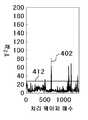
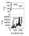
도 4a 내지 도 4d에는, 1,400샘플(웨이퍼)의 연속 처리를 행했을 경우의, 장치 건강도를 나타내는 T2값을, 각 방법으로 계산했을 경우의 결과를 나타낸다.4A to 4D show the results of calculating the T2 value representing the device health level in the case of performing continuous processing of 1,400 samples (wafers) by each method.
도 4a에는, 장치 건강도를 나타내는 T2값을, 모든 특징량을 사용하여 이상 검출을 행했을 경우의 처리 웨이퍼 매수와 T2값:401과의 관계를 나타낸다. 도면 중, 411은, 이상 검출을 위한 기준이 되는 임계값을 나타내고 있다.In Fig. 4A, the relationship between the number of processed wafers and the T2 value:401 when abnormality detection is performed using all of the feature quantities for the T2 value representing the device health level. In the figure, 411 denotes a threshold value serving as a reference for abnormality detection.
또한, 도 4b에는, 비특허문헌 1에 기재된 방법으로 특징량 선택을 행하여 이상 검출을 실시했을 경우의 처리 웨이퍼 매수와 T2값:402와의 관계를 나타낸다. 도면 중, 412는, 이상 검출을 위한 기준이 되는 임계값을 나타내고 있다.In addition, FIG. 4B shows the relationship between the number of processed wafers and the T2 value:402 when abnormality detection is performed by selecting a feature amount by the method described in Non-Patent Document 1. In the figure, 412 denotes a threshold value serving as a criterion for abnormality detection.
또한, 도 4c에는, 본 실시예에 기재된 이상 검출 유닛(117)에 의해 이상 검출을 행했을 경우의 처리 웨이퍼 매수와 T2값:403과의 관계를 나타낸다. 도면 중, 413은, 이상 검출을 위한 기준이 되는 임계값을 나타내고 있다.In addition, Fig. 4C shows the relationship between the number of processed wafers and T2 value:403 when abnormality detection is performed by the
또한, 도 4d에는, 각 처리 웨이퍼마다 장치 건강도를 나타내는 T2값의 계산에 요한 시간을, 도 4a에 대응하는 모든 특징량을 사용하여 이상 검출을 행했을 경우와, 도 4b에 대응하는 비특허문헌 1에 기재된 방법으로 특징량 선택을 행하여 이상 검출을 실시했을 경우와, 도 4c에 대응하는 본 실시예에 기재된 이상 검출 유닛(117)에 의해 이상 검출을 행했을 경우의 3종류의 경우에 관해서 나타낸다.In addition, in FIG. 4D, the time required to calculate the T2 value representing the device health level for each processed wafer is compared with the case of performing abnormality detection using all the feature quantities corresponding to FIG. 4A and the ratio corresponding to FIG. 4B. In the case of performing abnormality detection by selecting a feature amount by the method described in Patent Document 1, and in the case of performing abnormality detection by the
도 4a에 나타내는 바와 같이, 모든 특징량을 사용했을 경우, 600번째의 샘플 이후에, 임계값(411)을 초과하는 이상이 빈번하게 검출되고 있다. 이 해석에 요한 계산 시간은 13.9s로 비교적 길다. 도 4b에 나타낸 비특허문헌 1에 기재된 방법으로 특징량 선택을 행했을 경우, 계산 시간은 1.60s 정도로 짧지만, 1,000 샘플 전부에 걸쳐, 임계값(412)을 초과하는 이상은 그다지 검출되고 있지 않아, 전체 특징량을 사용했을 때에 검출할 수 있었던 이상의 대다수의 부분을 간과하고 있다는 결과가 되었다.As shown in Fig. 4A, when all the feature quantities are used, an abnormality exceeding the
이에 대하여, 도 4c에 나타내는 바와 같이, 본 실시예에 기재된 방법에 의해 특징량 선택을 행했을 경우, 100번째의 샘플 이후에 임계값(413)을 초과하는 이상을 검출할 수 있으며, 또한, 도 4d에 나타내는 바와 같이, 계산에 요하는 시간도 0.972s로 전체 샘플을 이용했을 경우와 비교하여, 매우 짧은 시간에 이상 검출을 실시할 수 있었다.On the other hand, as shown in Fig. 4C, when the feature amount is selected by the method described in the present embodiment, an abnormality exceeding the
상기한 바와 같이 본 실시예에 있어서의 이상 검출 유닛(117)을 이용함으로써, 반도체 제조 중에 일어나는 플라스마 처리 장치(100)의 이상을 감도(感度) 좋게, 짧은 해석 시간에 검출할 수 있다.As described above, by using the
또한, 상기한 실시예에서는, 처리실(101)의 내부의 이상 검출을 행하는 예 에 대해서 설명했지만, 본 실시예는 이에 한정되는 것이 아니며, 반송실(130)이나, 도시하고 있지 않은 진공 배기 수단 및 가스 공급 수단에 대해서, 그들 각 수단에 마련한 센서로부터의 출력 신호를 받아 각 수단의 이상 검출을 행할 경우에 대해서도 적용할 수 있다. 즉, 본 실시예에 따른 발명은, 플라스마 처리 장치가 구비하는 각 구성 중 어느 것의 상태를 예측하는 것이다. 여기에서, 「플라스마 처리 장치가 구비하는 각 구성」이란, 예를 들면, 「처리실(101)」, 「반송실」 등을 말한다.In addition, in the above-described embodiment, an example in which abnormality detection inside the
[실시예 2][Example 2]
실시예 2에 있어서는, 장치 건강도를 계산하기 위한 부하를 실시예 1의 경우와 비교하여 더 경감하는 방법에 대해서, 실시예 1과 다른 구성의 부분에 대해서 설명한다.In Example 2, a method of further reducing the load for calculating the device health level compared to the case of Example 1 will be described with respect to a configuration different from that of Example 1.
본 실시예에 있어서의 장치 구성은, 실시예 1에서 도 1을 이용하여 설명한 플라스마 처리 장치(100)의 구성에 대하여, 장치 상태 이상 검출부(220)의 이상 검출 유닛(217) 이외는 같으므로, 이상 검출 유닛(217) 이외의 설명을 생략한다.The device configuration in this embodiment is the same as the configuration of the
도 5는, 본 실시예에 따른 장치 상태 이상 검출부(220)의 이상 검출 유닛(217)의 구성을 나타내는 블록도이다. 본 실시예에 따른 이상 검출 유닛(217)은, 데이터 취득부(2171), 연산부(2172), 특징량 랭킹 작성부(2173), 특징량 선택부(2174), 장치 건강도 계산부(2175), 장치 건강도 임계값 계산부(2176), 재표준화부(2177), 비교부(2178), 출력부(2179)를 구비하고, 특징량 추출부(116)에서 추출한 각종 특징량의 정보를 이용하여 이상 검출을 행하고, 그 결과를, 출력부(2179)로부터 외부로 출력한다.5 is a block diagram showing the configuration of the
도 6은, 도 5의 이상 검출 유닛(217)에서 본 실시예에 의해 실행되는 이상 검출 공정의 플로우 차트이다.6 is a flowchart of an abnormality detection process performed by the
이상 검출의 제1 공정(S601)에 있어서, 데이터 취득부(2171)에 있어서, 특징량 추출부(116)에서 추출한 정상인 에칭 장치 상태일 경우의 데이터만으로 이루어지는 데이터군을, 복수의 샘플에 대해서 트레이닝 데이터군을 취득한다.In the first process of abnormality detection (S601), in the
이상 검출의 제2 공정(S602)에 있어서, S601에서 데이터 취득부(2171)에 의해 취득한 트레이닝 데이터를 바탕으로, 연산부(2172)에 있어서, 정상인 장치 상태에 있어서의 각 특징량의 전체 샘플의 평균값과 표준편차값을 계산한다.In the second step of abnormality detection (S602), based on the training data acquired by the
이상 검출의 제3 공정(S603)에 있어서, 연산부(2172)에서, S601에서 취득한 트레이닝 데이터 중의 각각의 샘플의 각 특징량의 값으로부터, S602에 있어서 계산된 트레이닝 데이터에 있어서의 각 특징량의 전체 샘플의 평균값을 뺀다(감산 처리). 또한 연산부(2172)는, 이 감산 처리에 의해 얻어진 값을, S602에 있어서 계산된 트레이닝 데이터에 있어서의 각 특징량의 전체 샘플의 표준편차값으로 제산하여 트레이닝 데이터의 표준화 처리를 행한다. 이 트레이닝 데이터의 표준화 처리는, 실시예 1에서 설명한 S303에 있어서의 트레이닝 데이터의 표준화 처리와 같은 처리를 행한다.In the third step of abnormality detection (S603), in the
이상 검출의 제4 공정(S604)에 있어서, 특징량 랭킹 작성부(2173)에 있어서, 제3 공정(S603)에서 연산부(2172)에서 표준화된 트레이닝 데이터에 있어서, 표준화 후의 값이 큰 순으로 특징량의 랭킹을 작성하고, 특징량 선택부(2174)에 있어서, 특징량 랭킹 작성부(2173)에서 작성한 랭킹 중 미리 결정된 수의 특징량을 랭킹이 높은 순으로 선택한다. 예를 들면, 10개의 특징량을 선택할 경우, 랭킹 1위부터 10위까지의 특징량이 선택된다. 이 선택이 모든 샘플에 걸쳐 실시된다.In the fourth step of abnormality detection (S604), in the feature quantity ranking
여기에서, 새롭게 선택된 특징량(신(新)특징량)에 의한 신특징량 행렬이 작성되지만, 이 신특징량 행렬의 열 벡터는 다양한 특징량의 값이 혼합된 벡터가 된다. 이제부터는, 이 다양한 특징량이 혼합된 각각의 열 벡터가, 각각의 특징량으로 간주된다.Here, a new feature quantity matrix is created based on the newly selected feature quantity (new feature quantity), but the column vector of this new feature quantity matrix becomes a vector in which values of various feature quantities are mixed. From now on, each column vector in which these various feature quantities are mixed is regarded as each feature quantity.
이상 검출의 제5 공정(S605)에 있어서, 연산부(2172)는, 제4 공정(S604)에서 얻어진 신특징량 행렬을 바탕으로, 각 특징량의 평균값과 표준편차값을 계산한다.In the fifth step (S605) of abnormality detection, the
이상 검출의 제6 공정(S606)에 있어서, 연산부(2172)는, 제4 공정(S604)에서 특징량 선택부(2174)에 의해 작성된 신특징량 행렬을, 제5 공정(S605)에서 연산부(2172)에 의해 얻어진 평균값과 표준편차를 이용하여 표준화한다.In the sixth step (S606) of abnormality detection, the calculating
이상 검출의 제7 공정(S607)에 있어서는, 제6 공정(S606)에 의해 작성된 표준화한 특징량 행렬을 사용하여 주성분 분석을 실시하고, 그것에 수반하는 장치 건강도를 장치 건강도 계산부(2175)에서 계산하고, 장치 건강도의 임계값을 장치 건강도 임계값 계산부(2176)에서 계산한다. 장치 건강도 계산부(2175)에 있어서의 장치 건강도의 계산 방법은, 실시예 1의 S308의 공정에서 설명한 방법과 같으므로, 상세한 설명을 생략한다.In the seventh step (S607) of abnormality detection, principal component analysis is performed using the standardized feature quantity matrix created in the sixth step (S606), and the accompanying device health level is calculated by the device health
이상 검출의 제8 공정(S608)에 있어서, 데이터 취득부(2171)는, 특징량 추출부(116)로부터, 테스팅 데이터의 취득을 행한다. 또한, 이 테스팅 데이터는 단샘플에서의 취득으로 한다.In the eighth step (S608) of abnormality detection, the
이상 검출의 제9 공정(S609)에 있어서, 연산부(2172)는, 제8 공정(S608)에서 데이터 취득부(2171)에 의해 취득한 테스팅 데이터를, 제2 공정(S602)에 의해 구해진 평균값과 표준편차를 이용하여 표준화한다.In the ninth step (S609) of abnormality detection, the
이상 검출의 제10 공정(S610)에 있어서, 특징량 랭킹 작성부(2173)는, 제9 공정(S609)에 있어서 연산부(2172)에 의해 구해진 표준화한 테스팅 데이터에 있어서, 표준화 후의 값이 큰 순으로 특징량의 랭킹을 작성하고, 특징량 선택부(2174)에 있어서, 특징량 랭킹 작성부(2173)에서 작성한 랭킹 중 미리 결정된 수의 특징량을 랭킹이 높은 순으로 선택한다.In the tenth process of abnormality detection (S610), the feature quantity ranking
이상 검출의 제11 공정(S611)에 있어서, 재표준화부(2177)는, 제10 공정(S610)에 의해 정렬된 각각의 특징량을, 제5 공정(S605)에서 얻어진 평균값과 표준편차를 이용하여 재표준화한다.In the eleventh step (S611) of the abnormality detection, the
이상 검출의 제12 공정(S612)에 있어서, 장치 건강도 계산부(2175)는, 제11 공정(S611)에 의해 얻어진 재표준화한 특징량과, 제7 공정(S607)에 있어서 구해진 주성분 모델을 이용하여, 재표준화된 테스팅 데이터에 의한 장치 건강도를 계산한다.In the twelfth step (S612) of the abnormality detection, the device
이상 검출의 제13 공정(S613)에 있어서, 비교부(2178)는, 제12 공정(S612)에서 장치 건강도 계산부(2175)에 의해 계산한 이상 검출을 행하려는 처리에 있어서의 장치 건강도와 제7 공정(S607)에서 장치 건강도 계산부(2175)에 의해 구해진 건강도 임계값을 비교하여, 제12 공정(S612)에서 계산한 장치 건강도가 제7 공정(S707)에 의해 구해진 건강도 임계값보다도 크면(YES일 경우), 그 처리는 이상이라고 판단되고, 출력부(2179)로부터 이상에 관한 정보가 출력된다(S614).In the thirteenth step (S613) of the abnormality detection, the
한편, 제12 공정(S612)에서 계산한 장치 건강도가 제7 공정(S607)에 의해 구해진 건강도 임계값보다도 작아, 이상이라고 판단되지 않았을 경우(NO일 경우)에는, 다음 웨이퍼 처리가 실시되어, 이상 검출의 제8 공정(S608)으로 돌아간다.On the other hand, if the device health calculated in the twelfth step (S612) is less than the health level threshold value obtained in the seventh step (S607) and is not determined to be abnormal (in the case of NO), the next wafer processing is performed. , It returns to the eighth process (S608) of abnormality detection.
실시예 2의 방법에 있어서는, 정상인 장치 상태에 있어서의 각 샘플에 있어서도, 정상인 데이터의 평균값으로부터의 어긋남의 랭킹에 따라 특징량의 정렬을 행함으로써, 정상인 데이터의 평균값으로부터의 어긋남의 크기를 새로운 특징량으로서 다시 정의한다는 데이터 조작을 행하고 있다. 이 조작에 의해, 주성분 모델의 반복 작성을 행하지 않고, 테스팅 데이터마다의 정보를 해석에 도입하는 것이 가능해져, 실시예 1의 경우와 비교하여, 가일층의 계산 부하 저감을 실현할 수 있다.In the method of Example 2, the magnitude of the deviation from the average value of the normal data is determined by aligning the feature quantities according to the ranking of the deviation from the average value of the normal data, even for each sample in the normal device state. Data manipulation of redefining it as a quantity is being performed. By this operation, it becomes possible to introduce information for each testing data into the analysis without repeatedly creating a principal component model, and it is possible to realize a further reduction in the computational load compared to the case of Example 1.
이상, 본 발명을 실시형태에 의거하여 구체적으로 설명했지만, 본 발명은 상기 실시형태에 한정되지 않으며, 그 요지를 일탈하지 않는 범위에서 각종 변경 가능하다. 예를 들면, 본 실시예에서는 이상의 검출에 주성분 분석과 그것에 수반하는 Hotteling's T2을 이용하고 있지만, 그 밖의 이상 검출 수단을 이용해도 상관없다.As mentioned above, although this invention was demonstrated concretely based on embodiment, this invention is not limited to the said embodiment, Various changes can be made within the range which does not deviate from the summary. For example, in the present embodiment, principal component analysis and Hotteling's T2 accompanying it are used to detect abnormalities, but other abnormality detection means may be used.
예를 들면, 본 실시예에서는 센서 신호로부터 특징량을 추출하는 특징량 추출 수단과 이상 검출에 관한 해석을 행하는 이상 검출 유닛(217)이 장치의 제어 장치 등과는 무관하게 기재되어 있지만, 상기의 특징량 추출 수단이나 이상 검출 수단이 장치의 제어 장치 중에 도입되어 있는 구성이어도 상관없다. 또한 센서에 관해서는 몇 센서가 있어도 상관없다.For example, in the present embodiment, the feature quantity extraction means for extracting the feature quantity from the sensor signal and the
또한, 본 실시예도, 반송실(130)이나, 도시하고 있지 않은 진공 배기 수단 및 가스 공급 수단에 대해서, 그들 각 수단에 마련한 센서로부터의 출력 신호를 받아 각 수단의 이상 검출을 행할 경우에 대해서도 적용할 수 있다.In addition, the present embodiment is also applied to the case of detecting an abnormality of each means by receiving an output signal from a sensor provided in each of the means for the
또한, 본 실시예에서는, 플라스마 처리 장치에 대해서 본 발명을 적용한 예였지만, 플라스마 처리 장치 이외에 진공 처리 장치, 노광 장치, 성막(成膜) 장치, 어닐 장치 등의 반도체 제조 장치에도 적용 가능하다.In addition, in this embodiment, although the present invention was applied to a plasma processing apparatus, it is applicable to semiconductor manufacturing apparatuses such as a vacuum processing apparatus, an exposure apparatus, a film forming apparatus, and an annealing apparatus in addition to the plasma processing apparatus.
100: 플라스마 처리 장치 101: 처리실
102: 시료대 103: 웨이퍼
104: 고주파 전극 105: 고주파 전원
106: 마이크로파 전원 107: 마이크로파 발진원
108: 솔레노이드 코일109: 도파관
110: 내측의 정전 흡착 전극111: 외측의 정전 흡착 전극
112: 유전체층 113: 내측의 가변 직류 전원
114: 외측의 가변 직류 전원 115: 데이터 보존부
116: 특징량 추출부 117, 217: 이상 검출 유닛
118: 전압 모니터용 센서119: 압력 센서
120, 220: 장치 상태 이상 검출부100: plasma processing device 101: processing chamber
102: sample stand 103: wafer
104: high frequency electrode 105: high frequency power supply
106: microwave power supply 107: microwave oscillation source
108: solenoid coil 109: waveguide
110: inner electrostatic adsorption electrode 111: outer electrostatic adsorption electrode
112: dielectric layer 113: inner variable DC power supply
114: external variable DC power supply 115: data storage unit
116: feature
118: voltage monitor sensor 119: pressure sensor
120, 220: device status abnormality detection unit
Claims (7)
Translated fromKorean정상인 상태의 상기 플라스마 처리 장치의 모니터된 데이터로부터 상기 플라스마 처리 장치의 상태를 나타내는 제1 특징량이 구해지고,
상기 플라스마 처리 장치의 플라스마 처리시에 모니터된 데이터로부터 상기 플라스마 처리 장치의 상태를 나타내는 제2 특징량이 구해지고,
상기 구해진 제2 특징량이 상기 제1 특징량을 이용하여 연산되고,
상기 연산된 제2 특징량의 큰 것부터 순서대로 선택된 특징량과 동일한 종류의 상기 제1 특징량을 이용하여 상기 플라스마 처리 장치의 상태를 예측하는 모델이 생성되고,
상기 생성된 모델을 이용하여 상기 플라스마 처리 장치의 상태가 예측되는 것을 특징으로 하는 상태 예측 장치.In a state prediction device for predicting a state of a plasma processing device,
From the monitored data of the plasma processing device in a normal state, a first characteristic amount indicating the state of the plasma processing device is obtained,
A second feature amount indicating the state of the plasma processing device is obtained from data monitored during plasma processing of the plasma processing device,
The obtained second feature quantity is calculated using the first feature quantity,
A model for predicting the state of the plasma processing apparatus is generated using the first feature quantity of the same type as the feature quantity selected in order from the largest of the calculated second feature quantity,
The state prediction device, characterized in that the state of the plasma processing device is predicted using the generated model.
상기 생성된 모델은, 상기 플라스마 처리 장치의 상태를 예측할 때마다 갱신되는 것을 특징으로 하는 상태 예측 장치.The method of claim 1,
The generated model is updated every time a state of the plasma processing device is predicted.
상기 연산된 제2 특징량의 각각은, 복수의 플라스마 처리에 있어서의 상기 제1 특징량의 각각의 평균값을 상기 제2 특징량의 각각으로부터 감(減)한 값의 각각을 상기 복수의 플라스마 처리에 있어서의 상기 제1 특징량의 각각의 표준편차에 의해 나눈 값의 각각인 것을 특징으로 하는 상태 예측 장치.The method of claim 1,
For each of the calculated second feature quantities, each of the average values of each of the first feature quantities in a plurality of plasma processes is subtracted from each of the second feature quantities, and the plurality of plasmas are processed. The state prediction apparatus, characterized in that each of a value divided by each standard deviation of the first characteristic quantity in.
자(自)장치의 어느 개소(箇所)에 있어서의 정상인 상태시에 모니터된 데이터로부터 상기 자장치의 어느 개소에 있어서의 상태를 나타내는 제1 특징량이 구해지고,
상기 자장치의 어느 개소에 있어서의 상기 시료의 처리시에 모니터된 데이터로부터 상기 자장치의 어느 개소에 있어서의 상태를 나타내는 제2 특징량이 구해지고,
상기 구해진 제2 특징량이 상기 제1 특징량을 이용하여 연산되고,
상기 연산된 제2 특징량의 큰 것부터 순서대로 선택된 특징량과 동일한 종류의 상기 제1 특징량을 이용하여 상기 자장치의 어느 개소에 있어서의 상태를 예측하는 모델이 생성되고,
상기 생성된 모델을 이용하여 상기 자장치의 어느 개소에 있어서의 상태가 예측되는 제어 장치를 더 구비하는 것을 특징으로 하는 반도체 제조 장치.A semiconductor manufacturing apparatus comprising a processing chamber in which a sample is processed, and a conveying chamber connected to the processing chamber for conveying the sample to the processing chamber,
From the data monitored in a normal state at a certain point of the own device, a first characteristic amount indicating a state at a certain point of the own device is obtained,
From the data monitored during the processing of the sample at any location of the magnetic device, a second characteristic amount indicating the state at any location of the magnetic device is obtained,
The obtained second feature quantity is calculated using the first feature quantity,
A model for predicting a state at a certain location of the magnetic device is generated using the first feature quantity of the same type as the feature quantity selected sequentially from the largest of the calculated second feature quantity,
And a control device for predicting a state at a certain location of the magnetic device by using the generated model.
자장치의 어느 개소에 있어서의 정상인 상태시에 모니터된 데이터로부터 상기 자장치의 어느 개소에 있어서의 상태를 나타내는 제1 특징량이 구해지고,
상기 자장치의 어느 개소에 있어서의 상기 시료의 처리시에 모니터된 데이터로부터 상기 자장치의 어느 개소에 있어서의 상태를 나타내는 제2 특징량이 구해지고,
상기 구해진 제2 특징량이 상기 제1 특징량을 이용하여 연산되고,
상기 연산된 제2 특징량의 큰 것부터 순서대로 선택된 특징량과 동일한 종류의 상기 제1 특징량을 이용하여 상기 자장치의 어느 개소에 있어서의 상태를 예측하는 모델이 생성되고,
상기 생성된 모델을 이용하여 상기 자장치의 어느 개소에 있어서의 상태가 예측되는 상태 예측 장치를 더 구비하는 것을 특징으로 하는 반도체 제조 장치.A semiconductor manufacturing apparatus comprising a processing chamber in which a sample is processed, and a conveying chamber connected to the processing chamber for conveying the sample to the processing chamber,
From the monitored data in a normal state at a certain point of the own device, a first characteristic amount indicating a state at a certain point of the own device is obtained,
From the data monitored during the processing of the sample at any location of the magnetic device, a second characteristic amount indicating the state at any location of the magnetic device is obtained,
The obtained second feature quantity is calculated using the first feature quantity,
A model for predicting a state at a certain location of the magnetic device is generated using the first feature quantity of the same type as the feature quantity selected sequentially from the largest of the calculated second feature quantity,
And a state predicting device for predicting a state at a certain location of the magnetic device by using the generated model.
상기 자장치의 어느 개소는, 상기 처리실 또는 상기 반송실인 것을 특징으로 하는 반도체 제조 장치.The method according to claim 4 or 5,
A semiconductor manufacturing apparatus, wherein any portion of the magnetic device is the processing chamber or the transfer chamber.
상기 연산된 제2 특징량의 각각은, 복수의 처리에 있어서의 상기 제1 특징량의 각각의 평균값을 상기 제2 특징량의 각각으로부터 감한 값의 각각을 상기 복수의 처리에 있어서의 상기 제1 특징량의 각각의 표준편차에 의해 나눈 값의 각각인 것을 특징으로 하는 반도체 제조 장치.The method of claim 6,
Each of the calculated second feature quantities is a value obtained by subtracting the average value of each of the first feature quantities in a plurality of processes from each of the second feature quantities, and the first feature in the plurality of processes. A semiconductor manufacturing apparatus characterized in that it is each of a value divided by each standard deviation of the characteristic quantity.
Applications Claiming Priority (2)
| Application Number | Priority Date | Filing Date | Title |
|---|---|---|---|
| JP2018154589AJP6990634B2 (en) | 2018-08-21 | 2018-08-21 | State prediction device and semiconductor manufacturing device |
| JPJP-P-2018-154589 | 2018-08-21 |
Publications (2)
| Publication Number | Publication Date |
|---|---|
| KR20200021868A KR20200021868A (en) | 2020-03-02 |
| KR102206348B1true KR102206348B1 (en) | 2021-01-22 |
Family
ID=69587207
Family Applications (1)
| Application Number | Title | Priority Date | Filing Date |
|---|---|---|---|
| KR1020190045229AActiveKR102206348B1 (en) | 2018-08-21 | 2019-04-18 | State predicting apparatus and semiconductor manufacturing apparatus |
Country Status (4)
| Country | Link |
|---|---|
| US (1) | US12050455B2 (en) |
| JP (1) | JP6990634B2 (en) |
| KR (1) | KR102206348B1 (en) |
| TW (1) | TWI708275B (en) |
Families Citing this family (7)
| Publication number | Priority date | Publication date | Assignee | Title |
|---|---|---|---|---|
| KR102710723B1 (en) | 2021-03-24 | 2024-09-27 | 성균관대학교산학협력단 | A portable diagnostic device and method thereby |
| JP7702635B2 (en)* | 2021-04-13 | 2025-07-04 | パナソニックIpマネジメント株式会社 | Production facility monitoring system and production facility monitoring method |
| KR102797798B1 (en) | 2021-07-13 | 2025-04-22 | 주식회사 히타치하이테크 | Diagnostic device and diagnostic method and plasma processing device and semiconductor device manufacturing system |
| CN117121169A (en)* | 2022-03-24 | 2023-11-24 | 株式会社日立高新技术 | Device diagnosis system, device diagnosis device, semiconductor device manufacturing system, and device diagnosis method |
| JP2023156153A (en)* | 2022-04-12 | 2023-10-24 | 東京エレクトロン株式会社 | Processed data analysis method and information processing device |
| TW202406412A (en)* | 2022-07-15 | 2024-02-01 | 日商東京威力科創股份有限公司 | Plasma processing system, assistance device, assistance method, and assistance program |
| JP7690686B2 (en)* | 2023-03-17 | 2025-06-10 | 株式会社日立ハイテク | State prediction device, state prediction method, and state prediction system |
Citations (1)
| Publication number | Priority date | Publication date | Assignee | Title |
|---|---|---|---|---|
| JP4448335B2 (en) | 2004-01-08 | 2010-04-07 | 東京エレクトロン株式会社 | Plasma processing method and plasma processing apparatus |
Family Cites Families (21)
| Publication number | Priority date | Publication date | Assignee | Title |
|---|---|---|---|---|
| US6658423B1 (en)* | 2001-01-24 | 2003-12-02 | Google, Inc. | Detecting duplicate and near-duplicate files |
| JP4128339B2 (en)* | 2001-03-05 | 2008-07-30 | 株式会社日立製作所 | Process monitor for sample processing apparatus and method for manufacturing sample |
| US6616759B2 (en)* | 2001-09-06 | 2003-09-09 | Hitachi, Ltd. | Method of monitoring and/or controlling a semiconductor manufacturing apparatus and a system therefor |
| JP2003197609A (en)* | 2001-12-27 | 2003-07-11 | Tokyo Electron Ltd | Method for monitoring plasma treatment device, and plasma treatment device |
| TWI276162B (en)* | 2002-06-05 | 2007-03-11 | Tokyo Electron Ltd | Multi-variable analysis model forming method of processing apparatus, multi-variable analysis method for processing apparatus, control apparatus of processing apparatus, and control system of processing apparatus |
| AU2003245315A1 (en)* | 2002-06-28 | 2004-01-19 | Tokyo Electron Limited | Method and system for predicting process performance using material processing tool and sensor data |
| JP4464276B2 (en)* | 2002-08-13 | 2010-05-19 | 東京エレクトロン株式会社 | Plasma processing method and plasma processing apparatus |
| JP2004335841A (en)* | 2003-05-09 | 2004-11-25 | Tokyo Electron Ltd | Prediction system and prediction method for plasma treatment apparatus |
| CN100419983C (en) | 2003-05-16 | 2008-09-17 | 东京毅力科创株式会社 | Process system health index and method of using the same |
| JP2004349419A (en)* | 2003-05-21 | 2004-12-09 | Tokyo Electron Ltd | Method and device for judging cause of abnormality in plasma processor |
| US6993404B2 (en) | 2003-07-11 | 2006-01-31 | Mks Instruments, Inc. | Graphical user interface with process quality indicator |
| US7328126B2 (en)* | 2003-09-12 | 2008-02-05 | Tokyo Electron Limited | Method and system of diagnosing a processing system using adaptive multivariate analysis |
| US7596718B2 (en) | 2006-05-07 | 2009-09-29 | Applied Materials, Inc. | Ranged fault signatures for fault diagnosis |
| KR101117928B1 (en)* | 2010-06-07 | 2012-02-29 | 명지대학교 산학협력단 | Plasma process diagnosis system, method and apparatus of detecting an end point in the same |
| US9508529B2 (en)* | 2014-10-23 | 2016-11-29 | Lam Research Corporation | System, method and apparatus for RF power compensation in a plasma processing system |
| JP6553398B2 (en)* | 2015-05-12 | 2019-07-31 | 株式会社日立ハイテクノロジーズ | Plasma processing apparatus, data processing apparatus and data processing method |
| US10032681B2 (en)* | 2016-03-02 | 2018-07-24 | Lam Research Corporation | Etch metric sensitivity for endpoint detection |
| JP2018083958A (en) | 2016-11-21 | 2018-05-31 | 株式会社タムロン | Abnormality detection device for thin film deposition device and abnormality detection method for thin film deposition device |
| JP6676020B2 (en)* | 2017-09-20 | 2020-04-08 | 株式会社日立ハイテク | Plasma processing apparatus and plasma processing apparatus state prediction method |
| US11133204B2 (en)* | 2019-01-29 | 2021-09-28 | Applied Materials, Inc. | Chamber matching with neural networks in semiconductor equipment tools |
| CN111476263B (en)* | 2019-12-27 | 2024-02-09 | 江苏科技大学 | Bearing defect identification method based on SDAE and improved GWO-SVM |
- 2018
- 2018-08-21JPJP2018154589Apatent/JP6990634B2/enactiveActive
- 2019
- 2019-04-18KRKR1020190045229Apatent/KR102206348B1/enactiveActive
- 2019-05-30TWTW108118701Apatent/TWI708275B/enactive
- 2019-08-06USUS16/533,273patent/US12050455B2/enactiveActive
Patent Citations (1)
| Publication number | Priority date | Publication date | Assignee | Title |
|---|---|---|---|---|
| JP4448335B2 (en) | 2004-01-08 | 2010-04-07 | 東京エレクトロン株式会社 | Plasma processing method and plasma processing apparatus |
Also Published As
| Publication number | Publication date |
|---|---|
| KR20200021868A (en) | 2020-03-02 |
| JP6990634B2 (en) | 2022-02-03 |
| TW202009974A (en) | 2020-03-01 |
| JP2020031096A (en) | 2020-02-27 |
| US20200064820A1 (en) | 2020-02-27 |
| TWI708275B (en) | 2020-10-21 |
| US12050455B2 (en) | 2024-07-30 |
Similar Documents
| Publication | Publication Date | Title |
|---|---|---|
| KR102206348B1 (en) | State predicting apparatus and semiconductor manufacturing apparatus | |
| KR102033438B1 (en) | Plasma processing apparatus and plasma processing apparatus state prediction method | |
| US5288367A (en) | End-point detection | |
| US6985215B2 (en) | Plasma processing method and plasma processing apparatus | |
| US6908864B2 (en) | Pressure control method and processing device | |
| US6916396B2 (en) | Etching system and etching method | |
| JP5865125B2 (en) | Charged particle beam equipment | |
| JP2017112238A (en) | Plasma processing device and method for operating plasma processing device | |
| EP4020521A1 (en) | Device for high speed sensing of rf signals from rf plasma processing equipment | |
| KR102429079B1 (en) | Plasma treatment method and wavelength selection method used for plasma treatment | |
| US12085497B1 (en) | Nanoparticle analysis for ultra-low level concentrations of nanoparticles in fluid samples | |
| US11784031B2 (en) | Method of detecting radicals using mass spectrometry | |
| JP4274348B2 (en) | Process prediction method, processing apparatus, and process prediction program | |
| JPH10223499A (en) | Article manufacturing method, article manufacturing system, and method of operating a plurality of processing devices | |
| CN100359660C (en) | A method for detecting the end point of plasma etching process | |
| Tang et al. | Recognition of Ethylene Plasma Spectra 1D Data Based on Deep Convolutional Neural Networks. Electronics 2024, 13, 983 | |
| Kim et al. | Arc detection algorithm using Photo Multiplier Tubes |
Legal Events
| Date | Code | Title | Description |
|---|---|---|---|
| A201 | Request for examination | ||
| PA0109 | Patent application | Patent event code:PA01091R01D Comment text:Patent Application Patent event date:20190418 | |
| PA0201 | Request for examination | ||
| E902 | Notification of reason for refusal | ||
| PE0902 | Notice of grounds for rejection | Comment text:Notification of reason for refusal Patent event date:20200223 Patent event code:PE09021S01D | |
| PG1501 | Laying open of application | ||
| E701 | Decision to grant or registration of patent right | ||
| PE0701 | Decision of registration | Patent event code:PE07011S01D Comment text:Decision to Grant Registration Patent event date:20201104 | |
| GRNT | Written decision to grant | ||
| PR0701 | Registration of establishment | Comment text:Registration of Establishment Patent event date:20210118 Patent event code:PR07011E01D | |
| PR1002 | Payment of registration fee | Payment date:20210119 End annual number:3 Start annual number:1 | |
| PG1601 | Publication of registration | ||
| PR1001 | Payment of annual fee | Payment date:20241219 Start annual number:5 End annual number:5 |