KR102198250B1 - Display apparatus and driving method thereof - Google Patents
Display apparatus and driving method thereofDownload PDFInfo
- Publication number
- KR102198250B1 KR102198250B1KR1020140006822AKR20140006822AKR102198250B1KR 102198250 B1KR102198250 B1KR 102198250B1KR 1020140006822 AKR1020140006822 AKR 1020140006822AKR 20140006822 AKR20140006822 AKR 20140006822AKR 102198250 B1KR102198250 B1KR 102198250B1
- Authority
- KR
- South Korea
- Prior art keywords
- signal
- vertical synchronization
- synchronization start
- frequency
- video signal
- Prior art date
- Legal status (The legal status is an assumption and is not a legal conclusion. Google has not performed a legal analysis and makes no representation as to the accuracy of the status listed.)
- Expired - Fee Related
Links
Images


Classifications
- G—PHYSICS
- G09—EDUCATION; CRYPTOGRAPHY; DISPLAY; ADVERTISING; SEALS
- G09G—ARRANGEMENTS OR CIRCUITS FOR CONTROL OF INDICATING DEVICES USING STATIC MEANS TO PRESENT VARIABLE INFORMATION
- G09G3/00—Control arrangements or circuits, of interest only in connection with visual indicators other than cathode-ray tubes
- G09G3/20—Control arrangements or circuits, of interest only in connection with visual indicators other than cathode-ray tubes for presentation of an assembly of a number of characters, e.g. a page, by composing the assembly by combination of individual elements arranged in a matrix no fixed position being assigned to or needed to be assigned to the individual characters or partial characters
- G09G3/34—Control arrangements or circuits, of interest only in connection with visual indicators other than cathode-ray tubes for presentation of an assembly of a number of characters, e.g. a page, by composing the assembly by combination of individual elements arranged in a matrix no fixed position being assigned to or needed to be assigned to the individual characters or partial characters by control of light from an independent source
- G09G3/36—Control arrangements or circuits, of interest only in connection with visual indicators other than cathode-ray tubes for presentation of an assembly of a number of characters, e.g. a page, by composing the assembly by combination of individual elements arranged in a matrix no fixed position being assigned to or needed to be assigned to the individual characters or partial characters by control of light from an independent source using liquid crystals
- G09G3/3611—Control of matrices with row and column drivers
- G09G3/3648—Control of matrices with row and column drivers using an active matrix
- G—PHYSICS
- G09—EDUCATION; CRYPTOGRAPHY; DISPLAY; ADVERTISING; SEALS
- G09G—ARRANGEMENTS OR CIRCUITS FOR CONTROL OF INDICATING DEVICES USING STATIC MEANS TO PRESENT VARIABLE INFORMATION
- G09G3/00—Control arrangements or circuits, of interest only in connection with visual indicators other than cathode-ray tubes
- G09G3/20—Control arrangements or circuits, of interest only in connection with visual indicators other than cathode-ray tubes for presentation of an assembly of a number of characters, e.g. a page, by composing the assembly by combination of individual elements arranged in a matrix no fixed position being assigned to or needed to be assigned to the individual characters or partial characters
- G09G3/34—Control arrangements or circuits, of interest only in connection with visual indicators other than cathode-ray tubes for presentation of an assembly of a number of characters, e.g. a page, by composing the assembly by combination of individual elements arranged in a matrix no fixed position being assigned to or needed to be assigned to the individual characters or partial characters by control of light from an independent source
- G09G3/36—Control arrangements or circuits, of interest only in connection with visual indicators other than cathode-ray tubes for presentation of an assembly of a number of characters, e.g. a page, by composing the assembly by combination of individual elements arranged in a matrix no fixed position being assigned to or needed to be assigned to the individual characters or partial characters by control of light from an independent source using liquid crystals
- G09G3/3607—Control arrangements or circuits, of interest only in connection with visual indicators other than cathode-ray tubes for presentation of an assembly of a number of characters, e.g. a page, by composing the assembly by combination of individual elements arranged in a matrix no fixed position being assigned to or needed to be assigned to the individual characters or partial characters by control of light from an independent source using liquid crystals for displaying colours or for displaying grey scales with a specific pixel layout, e.g. using sub-pixels
- G—PHYSICS
- G09—EDUCATION; CRYPTOGRAPHY; DISPLAY; ADVERTISING; SEALS
- G09G—ARRANGEMENTS OR CIRCUITS FOR CONTROL OF INDICATING DEVICES USING STATIC MEANS TO PRESENT VARIABLE INFORMATION
- G09G3/00—Control arrangements or circuits, of interest only in connection with visual indicators other than cathode-ray tubes
- G09G3/20—Control arrangements or circuits, of interest only in connection with visual indicators other than cathode-ray tubes for presentation of an assembly of a number of characters, e.g. a page, by composing the assembly by combination of individual elements arranged in a matrix no fixed position being assigned to or needed to be assigned to the individual characters or partial characters
- G09G3/34—Control arrangements or circuits, of interest only in connection with visual indicators other than cathode-ray tubes for presentation of an assembly of a number of characters, e.g. a page, by composing the assembly by combination of individual elements arranged in a matrix no fixed position being assigned to or needed to be assigned to the individual characters or partial characters by control of light from an independent source
- G09G3/36—Control arrangements or circuits, of interest only in connection with visual indicators other than cathode-ray tubes for presentation of an assembly of a number of characters, e.g. a page, by composing the assembly by combination of individual elements arranged in a matrix no fixed position being assigned to or needed to be assigned to the individual characters or partial characters by control of light from an independent source using liquid crystals
- G09G3/3611—Control of matrices with row and column drivers
- G09G3/3614—Control of polarity reversal in general
- G—PHYSICS
- G09—EDUCATION; CRYPTOGRAPHY; DISPLAY; ADVERTISING; SEALS
- G09G—ARRANGEMENTS OR CIRCUITS FOR CONTROL OF INDICATING DEVICES USING STATIC MEANS TO PRESENT VARIABLE INFORMATION
- G09G2230/00—Details of flat display driving waveforms
- G—PHYSICS
- G09—EDUCATION; CRYPTOGRAPHY; DISPLAY; ADVERTISING; SEALS
- G09G—ARRANGEMENTS OR CIRCUITS FOR CONTROL OF INDICATING DEVICES USING STATIC MEANS TO PRESENT VARIABLE INFORMATION
- G09G2300/00—Aspects of the constitution of display devices
- G09G2300/04—Structural and physical details of display devices
- G09G2300/0404—Matrix technologies
- G09G2300/0408—Integration of the drivers onto the display substrate
- G—PHYSICS
- G09—EDUCATION; CRYPTOGRAPHY; DISPLAY; ADVERTISING; SEALS
- G09G—ARRANGEMENTS OR CIRCUITS FOR CONTROL OF INDICATING DEVICES USING STATIC MEANS TO PRESENT VARIABLE INFORMATION
- G09G2310/00—Command of the display device
- G09G2310/08—Details of timing specific for flat panels, other than clock recovery
- G—PHYSICS
- G09—EDUCATION; CRYPTOGRAPHY; DISPLAY; ADVERTISING; SEALS
- G09G—ARRANGEMENTS OR CIRCUITS FOR CONTROL OF INDICATING DEVICES USING STATIC MEANS TO PRESENT VARIABLE INFORMATION
- G09G2320/00—Control of display operating conditions
- G09G2320/02—Improving the quality of display appearance
- G09G2320/0209—Crosstalk reduction, i.e. to reduce direct or indirect influences of signals directed to a certain pixel of the displayed image on other pixels of said image, inclusive of influences affecting pixels in different frames or fields or sub-images which constitute a same image, e.g. left and right images of a stereoscopic display
- G—PHYSICS
- G09—EDUCATION; CRYPTOGRAPHY; DISPLAY; ADVERTISING; SEALS
- G09G—ARRANGEMENTS OR CIRCUITS FOR CONTROL OF INDICATING DEVICES USING STATIC MEANS TO PRESENT VARIABLE INFORMATION
- G09G2320/00—Control of display operating conditions
- G09G2320/02—Improving the quality of display appearance
- G09G2320/0219—Reducing feedthrough effects in active matrix panels, i.e. voltage changes on the scan electrode influencing the pixel voltage due to capacitive coupling
- G—PHYSICS
- G09—EDUCATION; CRYPTOGRAPHY; DISPLAY; ADVERTISING; SEALS
- G09G—ARRANGEMENTS OR CIRCUITS FOR CONTROL OF INDICATING DEVICES USING STATIC MEANS TO PRESENT VARIABLE INFORMATION
- G09G2320/00—Control of display operating conditions
- G09G2320/02—Improving the quality of display appearance
- G09G2320/0233—Improving the luminance or brightness uniformity across the screen
- G—PHYSICS
- G09—EDUCATION; CRYPTOGRAPHY; DISPLAY; ADVERTISING; SEALS
- G09G—ARRANGEMENTS OR CIRCUITS FOR CONTROL OF INDICATING DEVICES USING STATIC MEANS TO PRESENT VARIABLE INFORMATION
- G09G2320/00—Control of display operating conditions
- G09G2320/02—Improving the quality of display appearance
- G09G2320/0261—Improving the quality of display appearance in the context of movement of objects on the screen or movement of the observer relative to the screen
- G—PHYSICS
- G09—EDUCATION; CRYPTOGRAPHY; DISPLAY; ADVERTISING; SEALS
- G09G—ARRANGEMENTS OR CIRCUITS FOR CONTROL OF INDICATING DEVICES USING STATIC MEANS TO PRESENT VARIABLE INFORMATION
- G09G2320/00—Control of display operating conditions
- G09G2320/02—Improving the quality of display appearance
- G09G2320/029—Improving the quality of display appearance by monitoring one or more pixels in the display panel, e.g. by monitoring a fixed reference pixel
- G09G2320/0295—Improving the quality of display appearance by monitoring one or more pixels in the display panel, e.g. by monitoring a fixed reference pixel by monitoring each display pixel
- G—PHYSICS
- G09—EDUCATION; CRYPTOGRAPHY; DISPLAY; ADVERTISING; SEALS
- G09G—ARRANGEMENTS OR CIRCUITS FOR CONTROL OF INDICATING DEVICES USING STATIC MEANS TO PRESENT VARIABLE INFORMATION
- G09G2320/00—Control of display operating conditions
- G09G2320/10—Special adaptations of display systems for operation with variable images
- G09G2320/103—Detection of image changes, e.g. determination of an index representative of the image change
Landscapes
- Engineering & Computer Science (AREA)
- Chemical & Material Sciences (AREA)
- Crystallography & Structural Chemistry (AREA)
- Physics & Mathematics (AREA)
- Computer Hardware Design (AREA)
- General Physics & Mathematics (AREA)
- Theoretical Computer Science (AREA)
- Control Of Indicators Other Than Cathode Ray Tubes (AREA)
- Liquid Crystal Display Device Control (AREA)
Abstract
Translated fromKorean
Description
Translated fromKorean본 발명은 표시 장치 및 그것의 구동 방법에 관한 것이다.The present invention relates to a display device and a driving method thereof.
일반적으로 표시 장치는 영상을 표시하기 위한 표시 패널과 표시 패널을 구동하는 데이터 드라이버 및 게이트 드라이버를 포함한다. 표시 패널은 복수의 게이트 라인, 복수의 데이터 라인 및 복수의 픽셀들을 포함한다. 픽셀 각각은 박막 트랜지스터, 액정 커패시터 및 스토리지 커패시터를 포함한다. 데이터 드라이버는 데이터 라인들에 계조 전압을 출력하고, 게이트 드라이버는 게이트 라인들을 구동하기 위한 게이트 구동 신호를 출력한다.In general, a display device includes a display panel for displaying an image, a data driver and a gate driver for driving the display panel. The display panel includes a plurality of gate lines, a plurality of data lines, and a plurality of pixels. Each of the pixels includes a thin film transistor, a liquid crystal capacitor, and a storage capacitor. The data driver outputs gray voltage to the data lines, and the gate driver outputs a gate driving signal for driving the gate lines.
이러한 표시 장치는 표시하고자 하는 게이트 라인에 연결된 박막 트랜지스터의 게이트 전극에 게이트 온 전압을 인가한 후, 표시 영상에 대응하는 데이터 전압을 소스 전극에 인가하여 영상을 표시할 수 있다. 박막 트랜지스터가 턴 온 됨에 따라서 액정 커패시터 및 스토리지 커패시터에 인가된 데이터 전압은 박막 트랜지스터가 턴 오프된 후에도 소정 시간 지속되어야 한다. 그러나, 표시 패널의 제조 공정의 문제로 인해 박막 트랜지스터의 게이트 전극과 드레인 전극 사이에 존재하는 기생 커패시턴스 때문에 액정 커패시터 및 스토리지 커패시터에 인가된 실제 계조 전압에 왜곡이 생길 수 있다. 즉, 데이터 드라이버로부터 출력된 계조 전압과 액정 커패시터 및 스토리지 커패시터에 인가된 실제 계조 전압 간의 차가 발생할 수 있다. 이와 같이 왜곡된 전압을 킥백(kickback) 전압이라 한다. 킥백 전압이 커질수록 그리고 표시 패널 내 박막 트랜지스터들 간의 킥백 전압들의 편차가 커질수록 표시 패널에 표시되는 영상의 품질은 저하된다.Such a display device may display an image by applying a gate-on voltage to a gate electrode of a thin film transistor connected to a gate line to be displayed, and then applying a data voltage corresponding to the display image to the source electrode. As the thin film transistor is turned on, the data voltage applied to the liquid crystal capacitor and the storage capacitor must continue for a predetermined time even after the thin film transistor is turned off. However, due to a problem in the manufacturing process of the display panel, distortion may occur in the actual gray voltage applied to the liquid crystal capacitor and the storage capacitor due to the parasitic capacitance existing between the gate electrode and the drain electrode of the thin film transistor. That is, a difference may occur between the gray voltage output from the data driver and the actual gray voltage applied to the liquid crystal capacitor and the storage capacitor. This distorted voltage is referred to as a kickback voltage. As the kickback voltage increases and the deviation of the kickback voltages between thin film transistors in the display panel increases, the quality of the image displayed on the display panel deteriorates.
특히, 동영상이 표시 패널에 표시되는 경우 특정 영상 패턴에서 킥백 전압에 의한 휘도 차가 시인될 수 있다.In particular, when a moving picture is displayed on the display panel, a difference in luminance due to the kickback voltage may be visually recognized in a specific image pattern.
따라서 본 발명의 목적은 표시 품질이 향상된 표시 장치를 제공하는데 있다.Accordingly, an object of the present invention is to provide a display device with improved display quality.
본 발명의 다른 목적은 표시 품질을 향상시키기 위한 표시 장치의 구동 방법을 제공하는데 있다.Another object of the present invention is to provide a method of driving a display device to improve display quality.
이와 같은 목적을 달성하기 위한 본 발명의 일 특징에 의하면, 표시 장치는, 복수의 데이터 라인들과 복수의 게이트 라인들에 각각 연결된 복수의 픽셀들을 포함하는 표시 패널과, 상기 복수의 데이터 라인들을 구동하는 데이터 드라이버와, 수직 동기 시작 신호에 동기해서 상기 복수의 게이트 라인들을 구동하는 게이트 드라이버, 및 외부로부터 입력된 영상 신호 및 제어 신호에 응답해서 상기 데이터 드라이버 및 상기 게이트 드라이버를 제어하고, 상기 게이트 드라이버로 제공하기 위한 상기 수직 동기 시작 신호를 출력하되, 현재 프레임의 영상 신호가 이전 프레임의 영상 신호를 제1 방향으로 쉬프트한 영상 신호와 일치할 때 상기 수직 동기 시작 신호의 주파수를 변경하는 타이밍 컨트롤러를 포함한다.According to an aspect of the present invention for achieving the above object, a display device includes a display panel including a plurality of data lines and a plurality of pixels respectively connected to a plurality of gate lines, and drives the plurality of data lines. A data driver that drives the data driver, a gate driver that drives the plurality of gate lines in synchronization with a vertical synchronization start signal, and controls the data driver and the gate driver in response to an image signal and a control signal input from the outside, and the gate driver A timing controller configured to output the vertical synchronization start signal to be provided, but to change the frequency of the vertical synchronization start signal when the video signal of the current frame coincides with the video signal shifted in the first direction of the video signal of the previous frame. Include.
이 실시예에 있어서, 상기 타이밍 컨트롤러는, 상기 수직 동기 시작 신호에 동기해서 상기 게이트 드라이버로 제공하기 위한 데이터 인에이블 신호를 더 출력하되, 상기 데이터 인에이블 신호는 액티브 구간과 블랭크 구간을 포함한다.In this embodiment, the timing controller further outputs a data enable signal to be provided to the gate driver in synchronization with the vertical synchronization start signal, wherein the data enable signal includes an active period and a blank period.
이 실시예에 있어서, 상기 데이터 인에이블 신호의 상기 블랭크 구간은 상기 수직 동기 시작 신호의 주파수에 반비례한다.In this embodiment, the blank period of the data enable signal is inversely proportional to the frequency of the vertical synchronization start signal.
이 실시예에 있어서, 상기 타이밍 컨트롤러는, 상기 데이터 인에이블 신호에 동기해서 상기 데이터 드라이버로 제공하기 위한 수평 동기 시작 신호를 더 출력한다.In this embodiment, the timing controller further outputs a horizontal synchronization start signal to be provided to the data driver in synchronization with the data enable signal.
이 실시예에 있어서, 상기 타이밍 컨트롤러는, 상기 현재 프레임의 영상 신호가 상기 이전 프레임의 영상 신호를 상기 제1 방향으로 H(H는 양의 정수) 픽셀만큼 쉬프트한 영상 신호와 일치할 때 상기 수직 동기 시작 신호의 주파수를 변경한다.In this embodiment, the timing controller, when the video signal of the current frame coincides with the video signal shifted by H (H is a positive integer) pixels in the first direction, the vertical Change the frequency of the synchronization start signal.
이 실시예에 있어서, 상기 타이밍 컨트롤러는, 노말 모드에서 상기 수직 동기 시작 신호의 주파수가 60Hz일 때 상기 현재 프레임의 영상 신호가 상기 이전 프레임의 영상 신호를 상기 제1 방향으로 1 픽셀만큼 쉬프트한 영상 신호와 일치할 때 상기 수직 동기 시작 신호의 주파수를 변경한다.In this embodiment, the timing controller is an image obtained by shifting the image signal of the previous frame by 1 pixel in the first direction when the frequency of the vertical synchronization start signal is 60 Hz in the normal mode. When coincident with the signal, the frequency of the vertical synchronization start signal is changed.
이 실시예에 있어서, 상기 타이밍 컨트롤러는, 노말 모드에서 상기 수직 동기 시작 신호의 주파수가 120Hz일 때 상기 현재 프레임의 영상 신호가 이전 프레임의 영상 신호를 상기 제1 방향으로 2 픽셀만큼 쉬프트한 영상 신호와 일치할 때 상기 수직 동기 시작 신호의 주파수를 변경한다.In this embodiment, the timing controller is a video signal obtained by shifting the video signal of the previous frame by 2 pixels in the first direction when the frequency of the vertical synchronization start signal is 120 Hz in the normal mode. When coinciding with, the frequency of the vertical synchronization start signal is changed.
이 실시예에 있어서, 상기 타이밍 컨트롤러는, 상기 영상 신호를 상기 데이터 신호로 변환하는 영상 처리부와, 상기 영상 신호를 저장하고, 상기 이전 프레임의 영상 신호를 출력하는 버퍼와, 상기 제어 신호를 수신하고, 상기 영상 신호가 상기 표시 패널의 테스트 영역 내에 표시될 영상 신호인 지의 여부를 판별하고, 판별 결과에 대응하는 인에이블 신호를 출력하는 테스트 영역 판별부와, 상기 영상 신호를 상기 현재 프레임의 영상 신호로 수신하고, 상기 버퍼로부터의 상기 이전 프레임의 영상 신호를 수신하고, 상기 제어 신호 및 상기 인에이블 신호에 응답해서 상기 수직 동기 시작 신호를 출력하는 제어 신호 발생부를 포함한다.In this embodiment, the timing controller includes an image processing unit that converts the image signal into the data signal, a buffer that stores the image signal and outputs the image signal of the previous frame, and receives the control signal. , A test area determining unit that determines whether the video signal is an image signal to be displayed in the test area of the display panel, and outputs an enable signal corresponding to the determination result, and the video signal is a video signal of the current frame. And a control signal generator configured to receive the video signal from the buffer, receive the video signal of the previous frame, and output the vertical synchronization start signal in response to the control signal and the enable signal.
이 실시예에 있어서, 상기 제어 신호 발생부는, 상기 인에이블 신호가 활성 상태일 때 상기 현재 프레임의 영상 신호와 상기 이전 프레임의 영상 신호를 제1 방향으로 쉬프트한 영상 신호를 비교하고, 주파수 변경 신호를 출력하는 비교기, 및 상기 주파수 변경 신호 및 상기 제어 신호에 응답해서 상기 수직 동기 시작 신호를 출력하는 제어 신호 발생부를 포함한다.In this embodiment, the control signal generator, when the enable signal is active, compares an image signal obtained by shifting the image signal of the current frame and the image signal of the previous frame in a first direction, and a frequency change signal And a control signal generator configured to output the vertical synchronization start signal in response to the frequency change signal and the control signal.
이 실시예에 있어서, 상기 제어 신호 발생부는, 상기 수직 동기 시작 신호에 동기해서 상기 게이트 드라이버로 제공하기 위한 데이터 인에이블 신호를 더 출력한다. 상기 데이터 인에이블 신호는 액티브 구간과 블랭크 구간을 포함한다.In this embodiment, the control signal generator further outputs a data enable signal to be provided to the gate driver in synchronization with the vertical synchronization start signal. The data enable signal includes an active period and a blank period.
이 실시예에 있어서, 상기 데이터 인에이블 신호의 상기 블랭크 구간은 상기 수직 동기 시작 신호의 주파수에 반비례한다.In this embodiment, the blank period of the data enable signal is inversely proportional to the frequency of the vertical synchronization start signal.
이 실시예에 있어서, 상기 제어 신호 발생부는, 상기 데이터 인에이블 신호에 동기해서 상기 데이터 드라이버로 제공하기 위한 수평 동기 시작 신호를 더 출력한다.In this embodiment, the control signal generator further outputs a horizontal synchronization start signal to be provided to the data driver in synchronization with the data enable signal.
이 실시예에 있어서, 상기 제어 신호 발생부는, 상기 현재 프레임의 영상 신호가 이전 프레임의 영상 신호를 상기 제1 방향으로 H(H는 양의 정수) 픽셀만큼 쉬프트한 영상 신호와 일치할 때 상기 수직 동기 시작 신호의 주파수를 변경한다.In this embodiment, the control signal generator, when the image signal of the current frame matches the image signal shifted by H (H is a positive integer) pixels in the first direction, the vertical Change the frequency of the synchronization start signal.
이 실시예에 있어서, 상기 제어 신호 발생부는, 노말 모드에서 상기 수직 동기 시작 신호의 주파수가 60Hz일 때 상기 현재 프레임의 영상 신호가 이전 프레임의 영상 신호를 상기 제1 방향으로 1 픽셀만큼 쉬프트한 영상 신호와 일치할 때 상기 수직 동기 시작 신호의 주파수를 변경한다.In this embodiment, when the frequency of the vertical synchronization start signal is 60 Hz in the normal mode, the control signal generator is an image obtained by shifting the image signal of the previous frame by 1 pixel in the first direction. When coincident with the signal, the frequency of the vertical synchronization start signal is changed.
본 발명의 다른 특징에 따른 표시 장치의 구동 방법은: 현재 프레임의 영상 신호 및 제어 신호를 수신하는 단계와, 버퍼로부터 이전 프레임의 영상 신호를 수신하는 단계와, 수직 동기 시작 신호를 발생하는 단계와, 상기 현재 프레임의 영상 신호가 상기 이전 프레임의 영상 신호를 제1 방향으로 쉬프트한 영상 신호와 일치할 때 상기 수직 동기 시작 신호의 주파수를 변경하는 단계, 및 상기 수직 동기 시작 신호에 동기해서 상기 현재 프레임의 영상 신호 대응하는 데이터 신호를 표시 패널로 제공하는 단계를 포함한다.A method of driving a display device according to another aspect of the present invention includes: receiving an image signal and a control signal of a current frame, receiving an image signal of a previous frame from a buffer, and generating a vertical synchronization start signal; , Changing the frequency of the vertical synchronization start signal when the video signal of the current frame coincides with the video signal shifting the video signal of the previous frame in the first direction, and the current in synchronization with the vertical synchronization start signal And providing a data signal corresponding to the image signal of the frame to the display panel.
이 실시예에 있어서, 상기 수직 동기 시작 신호에 동기해서 액티브 구간과 블랭크 구간을 포함하는 데이터 인에이블 신호를 발생하는 단계를 더 포함하는 것을 특징으로 한다.In this embodiment, the method further comprises generating a data enable signal including an active period and a blank period in synchronization with the vertical synchronization start signal.
이 실시예에 있어서, 상기 데이터 인에이블 신호의 상기 블랭크 구간은 상기 수직 동기 시작 신호의 주파수에 반비례한다.In this embodiment, the blank period of the data enable signal is inversely proportional to the frequency of the vertical synchronization start signal.
이 실시예에 있어서, 상기 주파수 변경 단계는, 상기 현재 프레임의 영상 신호가 상기 이전 프레임의 영상 신호를 상기 제1 방향으로 H(H는 양의 정수) 픽셀만큼 쉬프트한 영상 신호와 일치할 때 상기 수직 동기 시작 신호의 주파수를 변경하는 단계를 포함한다.In this embodiment, in the step of changing the frequency, when the video signal of the current frame matches the video signal of the previous frame by H (H is a positive integer) pixels shifted in the first direction, the And changing the frequency of the vertical synchronization start signal.
이 실시예에 있어서, 상기 현재 프레임의 영상 신호가 테스트 영역에 표시될 영상 신호일 때 인에이블 신호를 활성화하는 단계를 더 포함한다. 상기 인에이블 신호가 활성 상태일 때 상기 주파수 변경 단계를 수행한다.In this embodiment, the step of activating an enable signal when the video signal of the current frame is an image signal to be displayed in the test area is further included. When the enable signal is active, the frequency changing step is performed.
이와 같은 본 발명에 의하면, 현재 프레임의 영상 신호가 이전 프레임의 영상 신호를 제1 방향으로 쉬프트한 영상 신호와 일치할 때 상기 수직 동기 시작 신호의 주파수를 변경함으로써 킥백 전압에 의한 휘도 차가 시인되는 것을 방지할 수 있다.According to the present invention, when the video signal of the current frame coincides with the video signal of the previous frame shifted in the first direction, the difference in luminance due to the kickback voltage is recognized by changing the frequency of the vertical synchronization start signal. Can be prevented.
도 1은 본 발명의 실시예에 따른 표시 장치를 보여주는 블록도이다.
도 2는 도 1에 도시된 표시 패널 내 서브 픽셀들의 배치 예를 보여주는 도면이다.
도 3은 도 1에 도시된 타이밍 컨트롤러가 발생하는 수직 동기 시작 신호의 일 예를 보여주는 타이밍도이다.
도 4는 표시 장치가 60Hz로 동작할 때 도 3에 도시된 제1 프레임동안 표시 패널에 표시되는 영상의 일 예를 보여주는 도면이다.
도 5는 표시 장치가 60Hz로 동작할 때 도 3에 도시된 제2 프레임동안 표시 패널에 표시되는 영상의 일 예를 보여주는 도면이다.
도 6은 표시 장치가 120Hz로 동작할 때 도 3에 도시된 제1 프레임 내 제1 서브 프레임동안 표시 패널에 표시되는 영상의 일 예를 보여주는 도면이다.
도 7은 표시 장치가 120Hz로 동작할 때 도 3에 도시된 제2 프레임 내 제1 서브 프레임동안 표시 패널에 표시되는 영상의 일 예를 보여주는 도면이다.
도 8은 도 1에 도시된 표시 패널 내 서브 픽셀들의 배치 예를 보여주는 도면이다.
도 9는 표시 장치가 60Hz로 동작할 때 도 3에 도시된 제1 프레임동안 표시 패널에 표시되는 영상의 일 예를 보여주는 도면이다.
도 10은 표시 장치가 60Hz로 동작할 때 도 3에 도시된 제2 프레임동안 표시 패널에 표시되는 영상의 일 예를 보여주는 도면이다.
도 11은 표시 장치가 120Hz로 동작할 때 도 3에 도시된 제1 프레임 내 제1 서브 프레임동안 표시 패널에 표시되는 영상의 일 예를 보여주는 도면이다.
도 12은 표시 장치가 120Hz로 동작할 때 도 3에 도시된 제2 프레임 내 제1 서브 프레임동안 표시 패널에 표시되는 영상의 일 예를 보여주는 도면이다.
도 13 및 도 14는 소정의 데이터 라인으로 제공되는 데이터 계조 전압을 예시적으로 보여주는 도면들이다.
도 15는 도 2에 도시된 엇갈림 구조의 표시 패널에 표시되는 영상의 왜곡 현상을 예시적으로 보여주는 도면이다.
도 16은 도 8에 도시된 비엇갈림 구조의 표시 패널에 표시되는 영상의 왜곡 현상을 예시적으로 보여주는 도면이다.
도 17은 도 1에 도시된 타이밍 컨트롤러의 본 발명의 실시예에 따른 구성을 보여주는 블록도이다.
도 18은 도 17에 도시된 제어 신호 발생부의 구성을 보여주는 블록도이다.
도 19는 도 1에 도시된 표시 패널의 테스트 영역의 예를 보여주는 도면이다.
도 20은 도 18에 도시된 비교기로부터 출력되는 주파수 변경 신호를 예시적으로 보여주는 타이밍도이다.
도 21 및 도 22은 도 18에 도시된 제어 신호 발생기에서 발생하는 수직 동기 시작 신호 및 출력 인에이블 신호의 타이밍도들이다.
도 23은 본 발명의 실시예에 따른 표시 장치의 구동 방법을 보여주는 플로우차트이다. 설명의 편의를 위하여 도 16에 도시된 타이밍 컨트롤러를 참조하여 표시 장치의 구동 방법을 설명한다.1 is a block diagram illustrating a display device according to an exemplary embodiment of the present invention.
FIG. 2 is a diagram illustrating an arrangement example of subpixels in the display panel illustrated in FIG. 1.
FIG. 3 is a timing diagram illustrating an example of a vertical synchronization start signal generated by the timing controller illustrated in FIG. 1.
FIG. 4 is a diagram illustrating an example of an image displayed on a display panel during a first frame shown in FIG. 3 when the display device operates at 60 Hz.
5 is a diagram illustrating an example of an image displayed on a display panel during a second frame shown in FIG. 3 when the display device operates at 60 Hz.
6 is a diagram illustrating an example of an image displayed on a display panel during a first sub-frame within a first frame shown in FIG. 3 when the display device operates at 120 Hz.
FIG. 7 is a diagram illustrating an example of an image displayed on a display panel during a first subframe within a second frame shown in FIG. 3 when the display device operates at 120Hz.
8 is a diagram illustrating an arrangement example of subpixels in the display panel illustrated in FIG. 1.
9 is a diagram illustrating an example of an image displayed on a display panel during the first frame shown in FIG. 3 when the display device operates at 60 Hz.
10 is a diagram illustrating an example of an image displayed on a display panel during a second frame shown in FIG. 3 when the display device operates at 60 Hz.
FIG. 11 is a diagram illustrating an example of an image displayed on a display panel during a first sub-frame within a first frame illustrated in FIG. 3 when the display device operates at 120 Hz.
12 is a diagram illustrating an example of an image displayed on a display panel during a first sub-frame within a second frame shown in FIG. 3 when the display device operates at 120 Hz.
13 and 14 are diagrams exemplarily showing a data gray voltage provided to a predetermined data line.
15 is a diagram illustrating a distortion phenomenon of an image displayed on a display panel having a staggered structure illustrated in FIG. 2.
16 is a diagram illustrating a distortion phenomenon of an image displayed on the display panel having a non-intersecting structure illustrated in FIG. 8.
17 is a block diagram showing the configuration of the timing controller shown in FIG. 1 according to an embodiment of the present invention.
18 is a block diagram showing a configuration of a control signal generator illustrated in FIG. 17.
19 is a diagram illustrating an example of a test area of the display panel shown in FIG. 1.
20 is a timing diagram exemplarily showing a frequency change signal output from the comparator shown in FIG. 18.
21 and 22 are timing diagrams of a vertical synchronization start signal and an output enable signal generated in the control signal generator shown in FIG. 18.
23 is a flowchart illustrating a method of driving a display device according to an exemplary embodiment of the present invention. For convenience of explanation, a method of driving the display device will be described with reference to the timing controller illustrated in FIG. 16.
이하 본 발명의 실시예를 첨부된 도면들을 참조하여 상세히 설명한다.Hereinafter, embodiments of the present invention will be described in detail with reference to the accompanying drawings.
도 1은 본 발명의 실시예에 따른 표시 장치를 보여주는 블록도이다.1 is a block diagram illustrating a display device according to an exemplary embodiment of the present invention.
도 1을 참조하면, 표시 장치(100)는 표시 패널(110), 타이밍 컨트롤러(120), 게이트 드라이버(130) 및 데이터 드라이버(140)를 포함한다.Referring to FIG. 1, the
표시 장치(100)는 액정 표시(Liquid Crystal Display, LCD) 장치, 플라즈마 패널 표시(Plasma Panel Display, PDP) 장치, 유기 전계 발광 다이오드(Organic Light Emitting Diode, OLED) 표시 장치, 전계 효과 표시(Field Emission Display, FED) 장치 중 어느 하나일 수 있다.The
표시 패널(110)은 제1 방향(D1)으로 신장된 복수의 게이트 라인들(GL1-GLn), 제2 방향(D2)으로 신장된 복수의 데이터 라인들(DL1-DLm) 및 그들에 각각 연결된 복수의 서브 픽셀들(SPX)을 포함한다. 복수의 데이터 라인들(DL1-DLm)과 복수의 게이트 라인들(GL1-GLn)은 서로 절연되어 있다. 각 서브 픽셀(SPX)은 대응하는 데이터 라인 및 게이트 라인에 연결된 스위칭 트랜지스터, 이에 연결된 액정 커패시터(crystal capacitor) 및 스토리지 커패시터(storage capacitor)를 포함한다.The
타이밍 컨트롤러(120)는 외부로부터 영상 신호(RGB) 및 이의 표시를 제어하기 위한 제어 신호(CTRL)를 수신한다. 예를 들면, 제어 신호(CTRL)는 수직 동기 신호, 수평 동기 신호, 메인 클럭 신호 및 데이터 인에이블 신호 등을 포함한다. 타이밍 컨트롤러(120)는 영상 신호(RGB)를 표시 패널(110)의 동작 조건에 맞게 처리한 데이터 신호(DATA)를 데이터 드라이버(140)로 제공한다. 타이밍 컨트롤러(120)는 제어 신호(CTRL)에 기초하여 수평 동기 시작 신호(STH), 클럭 신호(HCLK) 및 라인 래치 신호(TP)를 데이터 드라이버(140)로 제공하고, 수직 동기 시작 신호(STV), 출력 인에이블 신호(DE)를 게이트 드라이버(130)로 제공한다.The
타이밍 컨트롤러(120)는 현재 프레임의 영상 신호(RGB)가 이전 프레임의 영상 신호(RGB)를 제1 방향으로 쉬프트한 영상 신호와 일치할 때 수직 동기 시작 신호(STV)의 주파수를 변경한다. 출력 인에이블 신호(DE)는 표시 패널(110)에 영상이 표시되는 액티브 구간과 영상이 표시되지 않는 블랭크 구간을 포함한다. 타이밍 컨트롤러(120)는 수직 동기 시작 신호(STV)의 주파수가 변경됨에 따라서 출력 인에이블 신호(DE)의 블랭크 구간을 조절한다. 또한, 타이밍 컨트롤러(120)는 출력 인에이블 신호(DE)에 동기해서 수평 시작 신호(STH)를 발생한다. 타이밍 컨트롤러(120)가 발생하는 수직 동기 시작 신호(STV) 및 출력 인에이블 신호(DE)는 추후 상세히 설명된다.The
게이트 드라이버(130)는 타이밍 컨트롤러(120)로부터의 수직 동기 시작 신호(STV) 및 출력 인에이블 신호(DE)에 응답해서 복수의 게이트 라인들(GL1-GLn)을 구동한다.The
게이트 드라이버(130)는 비정질-실리콘 스위칭 트랜지스터(amorphous Silicon Thin Film Transistor a-Si TFT)를 이용한 ASG(Amorphous silicon gate), 산화물 반도체, 결정질 반도체, 다결정 반도체 등을 이용한 회로로 구현되어서 표시 패널(110)과 동일한 기판 상에 형성될 수 있다. 다른 예에서, 게이트 드라이버(130)는 게이트 구동 IC(Integrated circuit)로 구현되어서 표시 패널(110)의 일측에 연결될 수 있다.The
데이터 드라이버(140)는 타이밍 컨트롤러(120)로부터의 데이터 신호(DATA), 수평 동기 시작 신호(STH), 클럭 신호(HCLK) 및 라인 래치 신호(TP)에 응답해서 데이터 라인들(DL1-DLm)을 구동한다.The
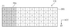
도 2는 도 1에 도시된 표시 패널 내 서브 픽셀들의 배치 예를 보여주는 도면이다.FIG. 2 is a diagram illustrating an arrangement example of subpixels in the display panel illustrated in FIG. 1.
도 2를 참조하면, 표시 패널(110) 내 하나의 서브 픽셀(SPX)은 레드, 그린 또는 블루에 대응하는 픽셀 전극(R, G, B) 중 어느 하나와 스위칭 트랜지스터를 포함한다. 이하 설명에서 레드에 대응하는 픽셀 전극을 포함하는 서브 픽셀은 레드 서브 픽셀, 그린에 대응하는 픽셀 전극을 포함하는 서브 픽셀은 그린 서브 픽셀 그리고 블루에 대응하는 픽셀 전극을 포함하는 서브 픽셀은 블루 서브 픽셀로 칭한다. 하나의 픽셀(PX)은 제1 방향(D1)으로 순차적으로 배열된 레드 서브 픽셀, 그린 서브 픽셀 및 블루 서브 픽셀을 포함한다.Referring to FIG. 2, one sub-pixel SPX in the
서브 픽셀(SPX) 내 스위칭 트랜지스터는 대응하는 데이터 라인과 대응하는 게이트 라인에 연결된다. 레드 서브 픽셀(Ri), 그린 서브 픽셀(Gi) 및 블루 서브 픽셀(Bi)은 게이트 라인의 신장 방향 즉, 제1 방향(D1)으로 순차적으로 배치되고, 데이터 라인의 신장 방향 즉, 제2 방향(D2)으로 동일한 색상의 픽셀들이 순차적으로 배열된다(단 i=1, 2, ..., n). 예컨대, 데이터 라인(DL1)의 우측에는 레드 서브 픽셀들(R1-Rn)이 배열되고, 데이터 라인들(DL2, DL3)의 사이에는 그린 서브 픽셀들(G1-Gn)이 배열되고, 그리고 데이터 라인들(DL3, DL4)의 사이에는 블루 서브 픽셀들(B1-Bn)이 배열된다. 이 실시예에서는 i번째 게이트 라인의 신장 방향인 제1 방향(D2)으로 레드 서브 픽셀, 그린 서브 픽셀 및 블루 서브 픽셀(Ri, Gi, Bi)이 순차적으로 배치된 것을 도시하고 설명하나, 픽셀들의 배치 순서는 (Ri, Bi, Gi), (Gi, Bi, Ri), (Gi, Ri, Bi), (Bi, Ri, Gi) 및 (Bi, Gi, Ri) 등과 같이 다양하게 변경될 수 있다.The switching transistor in the sub-pixel SPX is connected to a corresponding data line and a corresponding gate line. The red sub-pixel Ri, the green sub-pixel Gi, and the blue sub-pixel Bi are sequentially arranged in the extension direction of the gate line, that is, the first direction D1, and the extension direction of the data line, that is, the second direction. Pixels of the same color are sequentially arranged in (D2) (only i=1, 2, ..., n). For example, red subpixels R1-Rn are arranged on the right side of the data line DL1, green subpixels G1-Gn are arranged between the data lines DL2 and DL3, and the data line Blue subpixels B1-Bn are arranged between the fields DL3 and DL4. In this embodiment, a red sub-pixel, a green sub-pixel, and a blue sub-pixel Ri, Gi, and Bi are sequentially arranged in the first direction D2, which is an extension direction of the i-th gate line. The arrangement order can be variously changed, such as (Ri, Bi, Gi), (Gi, Bi, Ri), (Gi, Ri, Bi), (Bi, Ri, Gi) and (Bi, Gi, Ri). .
도 2를 참조하면, 레드 서브 픽셀들(R1-Rn), 그린 서브 픽셀들(G1-Gn) 및 블루 서브 픽셀들(B1-Bn) 중 일부는 좌측 인접 데이터 라인과 연결되고, 나머지는 우측 인접 데이터 라인과 연결된다. 구체적으로, 홀수 번째 게이트 라인들(GL1, GL3, …, GLn-1)과 연결된 레드 서브 픽셀들(R1, R3,..., Rn-1), 그린 서브 픽셀들(G1, G3, ..., Gn-1) 및 블루 서브 픽셀들(B1, B3, ..., Bn-1) 내 스위칭 트랜지스터들은 좌측 인접 데이터 라인들(DL1~DLn)과 연결되고, 짝수 번째 게이트 라인들(GL2, GL4, …, GLn)과 연결된 레드 서브 픽셀들(R2, R4,..., Rn), 그린 서브 픽셀들(G2, G4, ..., Gn) 및 블루 서브 픽셀들(B2, B4, ..., Bn) 내 스위칭 트랜지스터들은 우측 인접 데이터 라인들(DL1~DLn)과 연결된다. 이와 같은 연결 방법은 레드 서브 픽셀들(R1-Rn), 그린 서브 픽셀들(G1-Gn) 및 블루 서브 픽셀들(B1-Bn)이 제2 방향(D2)으로 매 서브 픽셀마다 좌측 및 우측 인접 데이터 라인들과 번갈아 연결된 엇갈림 구조이다.Referring to FIG. 2, some of the red sub-pixels R1-Rn, green sub-pixels G1-Gn, and blue sub-pixels B1-Bn are connected to a left adjacent data line, and others are adjacent to the right. It is connected to the data line. Specifically, the red sub-pixels R1, R3,..., Rn-1 connected to the odd-numbered gate lines GL1, GL3, ..., GLn-1, and the green sub-pixels G1, G3, .. ., Gn-1) and the switching transistors in the blue sub-pixels B1, B3, ..., Bn-1 are connected to the left adjacent data lines DL1 to DLn, and even gate lines GL2, Red sub-pixels R2, R4,..., Rn) connected to GL4, …, GLn, green sub-pixels G2, G4, ..., Gn, and blue sub-pixels B2, B4,. The switching transistors in .., Bn) are connected to the right adjacent data lines DL1 to DLn. In this connection method, the red sub-pixels R1-Rn, the green sub-pixels G1-Gn, and the blue sub-pixels B1-Bn are adjacent to the left and right for each sub-pixel in the second direction D2. It is an alternate structure connected to the data lines alternately.
데이터 라인들(DL1-DLm)은 컬럼 인버전 방식으로 구동된다. 컬럼 인버전 방식은 이웃한 데이터 라인들로 제공되는 계조 전압들의 전극들이 공통 전압(VCOM)을 기준으로 상보적이다.The data lines DL1 to DLm are driven in a column inversion method. In the column inversion method, electrodes of gray voltages provided to neighboring data lines are complementary based on a common voltage VCOM.
이러한 서브 픽셀들과 데이터 라인들의 연결에 의하면, 데이터 드라이버(140)에 의해서 데이터 라인들이 컬럼 인버전 방식으로 구동하더라도 화면에 나타나는 반전 즉, 겉보기 반전(apparent inversion)은 도트 인버전(dot inversion)과 동일하다. 즉, 인접한 서브 픽셀들로 제공되는 계조 전압들이 서로 상보적 극성을 갖는다. 겉보기 반전이 도트 인버전이 되면 계조 전압이 정극성 일 때와 부극성 일 때의 킥백(kick-back) 전압으로 인해서 나타나는 휘도의 차가 분산되므로 세로줄 플리커가 감소한다.According to the connection between the sub-pixels and the data lines, even if the data lines are driven in a column inversion method by the
도 3은 도 1에 도시된 타이밍 컨트롤러가 발생하는 수직 동기 시작 신호의 일 예를 보여주는 타이밍도이다.FIG. 3 is a timing diagram illustrating an example of a vertical synchronization start signal generated by the timing controller illustrated in FIG. 1.
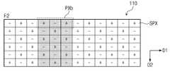
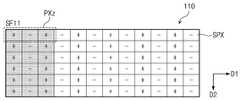
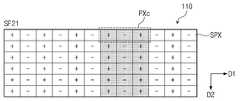
도 1 및 도 3을 참조하면, 표시 장치(100)가 60Hz로 동작하는 경우, 수직 동기 시작 신호(STV)의 주파수는 60Hz이다. 즉, 수직 동기 신호(STV)는 제1 프레임(F1) 및 제2 프레임(F2) 각각에서 하나의 펄스를 포함한다.1 and 3, when the
표시 장치(100)가 120Hz로 동작하는 경우, 수직 동기 시작 신호(STV)의 주파수는 120Hz이다. 즉, 수직 동기 신호(STV)는 제1 프레임(F1) 및 제2 프레임(F2) 각각에서 두 개의 펄스들을 포함한다. 표시 장치(100)가 120Hz로 동작하는 경우, 제1 프레임(F1)은 제1 서브 프레임(SF11) 및 제2 서브 프레임(SF12)을 포함하고, 제2 프레임(F2)은 제1 서브 프레임(SF21) 및 제2 서브 프레임(SF22)을 포함한다.When the
도 4는 표시 장치가 60Hz로 동작할 때 도 3에 도시된 제1 프레임동안 표시 패널에 표시되는 영상의 일 예를 보여주는 도면이다. 도 5는 표시 장치가 60Hz로 동작할 때 도 3에 도시된 제2 프레임동안 표시 패널에 표시되는 영상의 일 예를 보여주는 도면이다. 도 4 및 도 5에 도시된 표시 패널은 도 2에 도시된 엇갈림 구조를 갖는다.FIG. 4 is a diagram illustrating an example of an image displayed on a display panel during a first frame shown in FIG. 3 when the display device operates at 60 Hz. 5 is a diagram illustrating an example of an image displayed on a display panel during a second frame shown in FIG. 3 when the display device operates at 60 Hz. The display panels shown in FIGS. 4 and 5 have an alternate structure shown in FIG. 2.
도 1 및 도 3 내지 도 5를 참조하면, 표시 패널(110)은 4x6 개의 픽셀들을 포함한다. 이 실시예에서, 표시 패널(110)이 4x6 개의 픽셀들을 포함하는 것을 일 예로 도시하고 설명하나, 표시 패널(110)에 배열되는 픽셀들의 수는 해상도에 따라서 1920x1080, 2560x1440, 3840x2160 중 어느 하나일 수 있다.1 and 3 to 5, the
제1 프레임(F1)에서 제1 픽셀(PXa)에 표시된 영상은 제2 프레임(F2)에서 제2 픽셀(PXb)로 이동한다. 즉, 제1 프레임(F1)에서 표시 패널(110)에 표시되는 영상은 제1 프레임(F1)과 연속한 제2 프레임에서 제1 방향(D1)으로 1픽셀만큼 이동한다.The image displayed on the first pixel PXa in the first frame F1 moves from the second frame F2 to the second pixel PXb. That is, the image displayed on the
표시 패널(110)이 컬럼 인버전 방식으로 구동되는 경우, 제1 프레임(F1)에서 제1 픽셀(PXa) 내 레드 서브 픽셀, 그린 서브 픽셀 및 블루 서브 픽셀은 각각 정극성(+), 음극성(-) 및 정극성(+)으로 구동된다. 제2 프레임(F1)에서 제2 픽셀(PXb) 내 레드 서브 픽셀, 그린 서브 픽셀 및 블루 서브 픽셀은 각각 정극성(+), 음극성(-) 및 정극성(+)으로 구동된다.When the
제1 프레임(F1)에서 제1 픽셀(PXa)에 표시된 영상이 제2 프레임(F2)에서 제2 픽셀(PXb)로 이동하는 경우 동일한 영상 신호가 정극성(+), 음극성(-) 및 정극성(+)으로 반복적으로 구동된다. 즉, 표시 패널(110)이 컬럼 인버전 방식으로 구동되더라도 표시 패널(110)에 표시된 영상은 고정된 극성으로 표시된다.When the image displayed in the first pixel PXa in the first frame F1 moves from the second frame F2 to the second pixel PXb, the same image signal is positive (+), negative (-), and It is driven repeatedly with positive polarity (+). That is, even if the
도 6은 표시 장치가 120Hz로 동작할 때 도 3에 도시된 제1 프레임 내 제1 서브 프레임동안 표시 패널에 표시되는 영상의 일 예를 보여주는 도면이다. 도 7은 표시 장치가 120Hz로 동작할 때 도 3에 도시된 제2 프레임 내 제1 서브 프레임동안 표시 패널에 표시되는 영상의 일 예를 보여주는 도면이다. 도 6 및 도 7에 도시된 표시 패널은 도 2에 도시된 엇갈림 구조를 갖는다.6 is a diagram illustrating an example of an image displayed on a display panel during a first sub-frame within a first frame shown in FIG. 3 when the display device operates at 120 Hz. FIG. 7 is a diagram illustrating an example of an image displayed on a display panel during a first subframe within a second frame shown in FIG. 3 when the display device operates at 120Hz. The display panels shown in FIGS. 6 and 7 have an alternate structure shown in FIG. 2.
도 1, 도 3, 도 6 및 도 7을 참조하면, 표시 패널(110)은 4x6 개의 픽셀들을 포함한다. 이 실시예에서, 표시 패널(110)이 4x6 개의 픽셀들을 포함하는 것을 일 예로 도시하고 설명하나, 표시 패널(110)에 배열되는 픽셀들의 수는 해상도에 따라서 1920x1080, 2560x1440, 3840x2160 중 어느 하나일 수 있다.1, 3, 6, and 7, the
제1 프레임 내 제1 서브 프레임(SF11)에서 제1 픽셀(PXa)에 표시된 영상은 제2 프레임(F2) 내 제1 서브 프레임(SF21)에서 제2 픽셀(PXb)로 이동한다. 즉, 제1 프레임 내 제1 서브 프레임(SF11)에서 표시 패널(110)에 표시되는 영상은 제2 프레임(F2) 내 제1 서브 프레임(SF21)에서 제1 방향(D1)으로 2픽셀만큼 이동한다.The image displayed on the first pixel PXa in the first subframe SF11 in the first frame moves from the first subframe SF21 in the second frame F2 to the second pixel PXb. That is, the image displayed on the
표시 패널(110)이 컬럼 인버전 방식으로 구동되는 경우, 제1 프레임 내 제1 서브 프레임(SF11)에서 제1 픽셀(PXa) 내 레드 서브 픽셀, 그린 서브 픽셀 및 블루 서브 픽셀은 각각 정극성(+), 음극성(-) 및 정극성(+)으로 구동된다. 제2 프레임(F2) 내 제1 서브 프레임(SF21)에서 제2 픽셀(PXb) 내 레드 서브 픽셀, 그린 서브 픽셀 및 블루 서브 픽셀은 각각 정극성(+), 음극성(-) 및 정극성(+)으로 구동된다.When the
제1 프레임 내 제1 서브 프레임(SF11)에서 제1 픽셀(PXa)에 표시된 영상이 제2 프레임(F2) 내 제1 서브 프레임(SF21) 제2 픽셀(PXb)로 이동하는 경우 동일한 영상 신호가 정극성(+), 음극성(-) 및 정극성(+)으로 반복적으로 구동된다. 즉, 표시 패널(110)이 컬럼 인버전 방식으로 구동되더라도 표시 패널(110)에 표시된 영상은 고정된 극성으로 표시된다.When the image displayed in the first pixel PXa in the first sub-frame SF11 in the first frame moves to the second pixel PXb in the first sub-frame SF21 in the second frame F2, the same image signal is It is repeatedly driven with positive polarity (+), negative polarity (-) and positive polarity (+). That is, even if the
도 8은 도 1에 도시된 표시 패널 내 서브 픽셀들의 배치 예를 보여주는 도면이다.8 is a diagram illustrating an arrangement example of subpixels in the display panel illustrated in FIG. 1.
도 8을 참조하면, 표시 패널(110) 내 하나의 서브 픽셀(SPX)은 레드, 그린 또는 블루에 대응하는 픽셀 전극(R, G, B) 중 어느 하나와 스위칭 트랜지스터를 포함한다. 이하 설명에서 레드에 대응하는 픽셀 전극을 포함하는 서브 픽셀은 레드 서브 픽셀, 그린에 대응하는 픽셀 전극을 포함하는 서브 픽셀은 그린 서브 픽셀 그리고 블루에 대응하는 픽셀 전극을 포함하는 서브 픽셀은 블루 서브 픽셀로 칭한다. 하나의 픽셀(PX)은 제1 방향(D1)으로 순차적으로 배열된 레드 서브 픽셀, 그린 서브 픽셀 및 블루 서브 픽셀을 포함한다.Referring to FIG. 8, one sub-pixel SPX in the
레드 서브 픽셀(Ri), 그린 서브 픽셀(Gi) 및 블루 서브 픽셀(Bi)은 게이트 라인의 신장 방향 즉, 제1 방향(D1)으로 순차적으로 배치되고, 데이터 라인의 신장 방향 즉, 제2 방향(D2)으로 동일한 색상의 픽셀들이 순차적으로 배열된다(단 i=1, 2, ..., n). 예컨대, 데이터 라인(DL1)의 우측에는 레드 서브 픽셀들(R1-Rn)이 배열되고, 데이터 라인들(DL2, DL3)의 사이에는 그린 서브 픽셀들(G1-Gn)이 배열되고, 그리고 데이터 라인들(DL3, DL4)의 사이에는 블루 서브 픽셀들(B1-Bn)이 배열된다. 이 실시예에서는 i번째 게이트 라인의 신장 방향인 제1 방향(D1)으로 레드 서브 픽셀, 그린 서브 픽셀 및 블루 서브 픽셀(Ri, Gi, Bi)이 순차적으로 배치된 것을 도시하고 설명하나, 픽셀들의 배치 순서는 (Ri, Bi, Gi), (Gi, Bi, Ri), (Gi, Ri, Bi), (Bi, Ri, Gi) 및 (Bi, Gi, Ri) 등과 같이 다양하게 변경될 수 있다.The red sub-pixel Ri, the green sub-pixel Gi, and the blue sub-pixel Bi are sequentially arranged in the extension direction of the gate line, that is, the first direction D1, and the extension direction of the data line, that is, the second direction. Pixels of the same color are sequentially arranged in (D2) (only i=1, 2, ..., n). For example, red subpixels R1-Rn are arranged on the right side of the data line DL1, green subpixels G1-Gn are arranged between the data lines DL2 and DL3, and the data line Blue subpixels B1-Bn are arranged between the fields DL3 and DL4. In this embodiment, a red sub-pixel, a green sub-pixel, and a blue sub-pixel (Ri, Gi, Bi) are sequentially arranged in the first direction D1, which is an extension direction of the i-th gate line. The arrangement order can be variously changed, such as (Ri, Bi, Gi), (Gi, Bi, Ri), (Gi, Ri, Bi), (Bi, Ri, Gi) and (Bi, Gi, Ri). .
도 8을 참조하면, 레드 서브 픽셀들(R1-Rn), 그린 서브 픽셀들(G1-Gn) 및 블루 서브 픽셀들(B1-Bn)은 좌측 인접 데이터 라인과 연결된다. 이와 같은 연결 방법은 비엇갈림 구조이다.Referring to FIG. 8, red sub-pixels R1-Rn, green sub-pixels G1-Gn, and blue sub-pixels B1-Bn are connected to a left adjacent data line. This connection method is a non-intersecting structure.
데이터 라인들(DL1-DLm)은 컬럼 인버전 방식으로 구동된다. 컬럼 인버전 방식은 동일한 데이터 라인에 인가되는 계조 전압의 극성은 동일하고 이웃한 데이터 라인들로 제공되는 계조 전압들의 전극들이 공통 전압(VCOM)을 기준으로 상보적이다. 즉, 제1 방향(D1)으로 인접한 서브 픽셀들로 제공되는 계조 전압들이 서로 상보적 극성을 갖는다.The data lines DL1 to DLm are driven in a column inversion method. In the column inversion method, the polarity of gray voltages applied to the same data line is the same, and electrodes of gray voltages provided to neighboring data lines are complementary based on the common voltage VCOM. That is, gray voltages provided to the subpixels adjacent in the first direction D1 have complementary polarities.
도 9는 표시 장치가 60Hz로 동작할 때 도 3에 도시된 제1 프레임동안 표시 패널에 표시되는 영상의 일 예를 보여주는 도면이다. 도 10은 표시 장치가 60Hz로 동작할 때 도 3에 도시된 제2 프레임동안 표시 패널에 표시되는 영상의 일 예를 보여주는 도면이다. 도 9 및 도 10에 도시된 표시 패널은 도 8에 도시된 비엇갈림 구조를 갖는다.9 is a diagram illustrating an example of an image displayed on a display panel during the first frame shown in FIG. 3 when the display device operates at 60 Hz. 10 is a diagram illustrating an example of an image displayed on a display panel during a second frame shown in FIG. 3 when the display device operates at 60 Hz. The display panels shown in FIGS. 9 and 10 have a non-intersecting structure shown in FIG. 8.
도 1, 도 3, 도 9 및 도 10을 참조하면, 표시 패널(110)은 4x6 개의 픽셀들을 포함한다. 이 실시예에서, 표시 패널(110)이 4x6 개의 픽셀들을 포함하는 것을 일 예로 도시하고 설명하나, 표시 패널(110)에 배열되는 픽셀들의 수는 해상도에 따라서 1920x1080, 2560x1440, 3840x2160 중 어느 하나일 수 있다.1, 3, 9, and 10, the
제1 프레임(F1)에서 제1 픽셀(PXa)에 표시된 영상은 제2 프레임(F2)에서 제2 픽셀(PXb)로 이동한다. 즉, 제1 프레임(F1)에서 표시 패널(110)에 표시되는 영상은 제1 프레임(F1)과 연속한 제2 프레임에서 제1 방향(D1)으로 1픽셀만큼 이동한다.The image displayed on the first pixel PXa in the first frame F1 moves from the second frame F2 to the second pixel PXb. That is, the image displayed on the
표시 패널(110)이 컬럼 인버전 방식으로 구동되는 경우, 제1 프레임(F1)에서 제1 픽셀(PXa) 내 레드 서브 픽셀, 그린 서브 픽셀 및 블루 서브 픽셀은 각각 정극성(+), 음극성(-) 및 정극성(+)으로 구동된다. 제2 프레임(F1)에서 제2 픽셀(PXb) 내 레드 서브 픽셀, 그린 서브 픽셀 및 블루 서브 픽셀은 각각 정극성(+), 음극성(-) 및 정극성(+)으로 구동된다.When the
제1 프레임(F1)에서 제1 픽셀(PXa)에 표시된 영상이 제2 프레임(F2)에서 제2 픽셀(PXb)로 이동하는 경우 동일한 영상 신호가 정극성(+), 음극성(-) 및 정극성(+)으로 반복적으로 구동된다. 즉, 표시 패널(110)이 컬럼 인버전 방식으로 구동되더라도 표시 패널(110)에 표시된 영상은 고정된 극성으로 표시된다.When the image displayed in the first pixel PXa in the first frame F1 moves from the second frame F2 to the second pixel PXb, the same image signal is positive (+), negative (-), and It is driven repeatedly with positive polarity (+). That is, even if the
도 11은 표시 장치가 120Hz로 동작할 때 도 3에 도시된 제1 프레임 내 제1 서브 프레임동안 표시 패널에 표시되는 영상의 일 예를 보여주는 도면이다. 도 12은 표시 장치가 120Hz로 동작할 때 도 3에 도시된 제2 프레임 내 제1 서브 프레임동안 표시 패널에 표시되는 영상의 일 예를 보여주는 도면이다. 도 11 및 도 12에 도시된 표시 패널은 도 8에 도시된 비엇갈림 구조를 갖는다.FIG. 11 is a diagram illustrating an example of an image displayed on a display panel during a first sub-frame within a first frame illustrated in FIG. 3 when the display device operates at 120 Hz. 12 is a diagram illustrating an example of an image displayed on a display panel during a first sub-frame within a second frame shown in FIG. 3 when the display device operates at 120 Hz. The display panels shown in FIGS. 11 and 12 have a non-intersecting structure shown in FIG. 8.
도 1, 도 3, 도 11 및 도 12를 참조하면, 표시 패널(110)은 4x6 개의 픽셀들을 포함한다. 이 실시예에서, 표시 패널(110)이 4x6 개의 픽셀들을 포함하는 것을 일 예로 도시하고 설명하나, 표시 패널(110)에 배열되는 픽셀들의 수는 해상도에 따라서 1920x1080, 2560x1440, 3840x2160 중 어느 하나일 수 있다.1, 3, 11, and 12, the
제1 프레임 내 제1 서브 프레임(SF11)에서 제1 픽셀(PXa)에 표시된 영상은 제2 프레임(F2) 내 제1 서브 프레임(SF21)에서 제2 픽셀(PXb)로 이동한다. 즉, 제1 프레임 내 제1 서브 프레임(SF11)에서 표시 패널(110)에 표시되는 영상은 제2 프레임(F2) 내 제1 서브 프레임(SF21)에서 제1 방향(D1)으로 2픽셀만큼 이동한다.The image displayed on the first pixel PXa in the first subframe SF11 in the first frame moves from the first subframe SF21 in the second frame F2 to the second pixel PXb. That is, the image displayed on the
표시 패널(110)이 컬럼 인버전 방식으로 구동되는 경우, 제1 프레임 내 제1 서브 프레임(SF11)에서 제1 픽셀(PXa) 내 레드 서브 픽셀, 그린 서브 픽셀 및 블루 서브 픽셀은 각각 정극성(+), 음극성(-) 및 정극성(+)으로 구동된다. 제2 프레임(F2) 내 제1 서브 프레임(SF21)에서 제2 픽셀(PXb) 내 레드 서브 픽셀, 그린 서브 픽셀 및 블루 서브 픽셀은 각각 정극성(+), 음극성(-) 및 정극성(+)으로 구동된다.When the
제1 프레임 내 제1 서브 프레임(SF11)에서 제1 픽셀(PXa)에 표시된 영상이 제2 프레임(F2) 내 제1 서브 프레임(SF21) 제2 픽셀(PXb)로 이동하는 경우 동일한 영상 신호가 정극성(+), 음극성(-) 및 정극성(+)으로 반복적으로 구동된다. 즉, 표시 패널(110)이 컬럼 인버전 방식으로 구동되더라도 표시 패널(110)에 표시된 영상은 고정된 극성으로 표시된다.When the image displayed in the first pixel PXa in the first sub-frame SF11 in the first frame moves to the second pixel PXb in the first sub-frame SF21 in the second frame F2, the same image signal is It is repeatedly driven with positive polarity (+), negative polarity (-) and positive polarity (+). That is, even if the
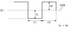
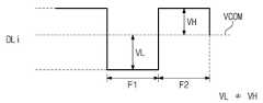
도 13 및 도 14는 소정의 데이터 라인으로 제공되는 데이터 계조 전압을 예시적으로 보여주는 도면들이다.13 and 14 are diagrams exemplarily showing a data gray voltage provided to a predetermined data line.
도 13 및 도 14를 참조하면, 표시 패널(110, 도 1에 도시됨)이 컬럼 인버전 방식으로 구동되는 경우 소정의 데이터 라인(DLi)으로 제공되는 계조 전압은 공통 전압(VCOM)을 기준으로 상보적이다. 이상적인 경우, 도 13에 도시된 바와 같이, 데이터 라인(DLi)으로 제공되는 정극성(+)의 계조 전압과 공통 전압(VCOM)의 차(VH)와 음극성(-)의 계조 전압과 공통 전압(VCOM)의 차(VL)가 같다(VH=VL).13 and 14, when the display panel 110 (shown in FIG. 1) is driven in a column inversion method, a gray voltage provided to a predetermined data line DL is based on a common voltage VCOM. It is complementary. In an ideal case, as shown in FIG. 13, the difference (VH) between the positive (+) gray voltage and the common voltage (VCOM) provided to the data line DLi and the negative (-) gray voltage and the common voltage The difference (VL) of (VCOM) is the same (VH=VL).
그러나, 스위칭 트랜지스터의 게이트 전극과 드레인 전극 사이에 존재하는 기생 커패시턴스 때문에 액정 커패시터에 인가된 계조 전압에 왜곡이 생길 수 있다. 이와 같이 왜곡된 전압을 킥백(kickback) 전압이라 한다. 킥백 전압에 의해서 실제 액정 커패시터로 제공되는 계조 전압은 공통 전압(VCOM)을 기준으로 정극성(+) 및 부극성(-) 중 어느 한쪽으로 치우치게 된다(VH≠VL).However, due to the parasitic capacitance existing between the gate electrode and the drain electrode of the switching transistor, distortion may occur in the gradation voltage applied to the liquid crystal capacitor. This distorted voltage is referred to as a kickback voltage. The gradation voltage that is actually provided to the liquid crystal capacitor by the kickback voltage is biased to either positive (+) or negative (-) polarity (VH≠VL) based on the common voltage (VCOM).
컬럼 인버전 방식으로 표시 패널(110)을 구동하는 경우, 하나의 픽셀(PX, 도 2에 도시됨) 내 레드 픽셀, 그린 픽셀 및 블루 픽셀의 휘도의 합이 하나의 색상으로 표시되므로 킥백 전압에 의한 휘도 변화가 인지되지 않는다.When the
도 15는 도 2에 도시된 엇갈림 구조의 표시 패널에 표시되는 영상의 왜곡 현상을 예시적으로 보여주는 도면이다.15 is a diagram illustrating a distortion phenomenon of an image displayed on a display panel having a staggered structure illustrated in FIG. 2.
도 4 및 도 5에서 설명한 바와 같이, 제1 프레임(F1)에서 표시 패널(110)에 표시된 영상이 제2 프레임(F2)에서 제1 방향(D1)으로 1 픽셀만큼 이동할 때 동일한 계조 전압이 동일한 극성으로 이동 표시되는 결과를 초래한다.4 and 5, when the image displayed on the
도 6 및 도 7에서 설명한 바와 같이, 제1 프레임(F1) 내 제1 서브 프레임(SF11)에서 표시 패널(110)에 표시된 영상이 제2 프레임(F2) 내 제1 서브 프레임(SF21)에서 제1 방향(D1)으로 2 픽셀만큼 이동할 때 동일한 계조 전압이 동일한 극성으로 이동 표시되는 결과를 초래한다.6 and 7, the image displayed on the
도 15를 참조하면, 제1 프레임(F1)에서 표시 패널(110)의 제1 영역(A1)에 표시된 영상이 제2 프레임(F2)에서 제1 방향(D1)으로 1 픽셀만큼 이동하여 제2 영역(A2)에 표시되는 것으로 가정한다. 이 경우, 제2 프레임(F2)에서 제2 영역(A2)에 표시된 영상은 체크 패턴으로 휘도 차가 발생하고, 이는 사용자에게 인지된다.Referring to FIG. 15, the image displayed in the first area A1 of the
도 16은 도 8에 도시된 비엇갈림 구조의 표시 패널에 표시되는 영상의 왜곡 현상을 예시적으로 보여주는 도면이다.16 is a diagram illustrating a distortion phenomenon of an image displayed on the display panel having a non-intersecting structure illustrated in FIG. 8.
도 9 및 도 10에서 설명한 바와 같이, 제1 프레임(F1)에서 표시 패널(110)에 표시된 영상이 제2 프레임(F2)에서 제1 방향(D1)으로 1 픽셀만큼 이동할 때 동일한 계조 전압이 동일한 극성으로 이동 표시되는 결과를 초래한다.As described in FIGS. 9 and 10, when the image displayed on the
도 11 및 도 12에서 설명한 바와 같이, 제1 프레임(F1) 내 제1 서브 프레임(SF11)에서 표시 패널(110)에 표시된 영상이 제2 프레임(F2) 내 제1 서브 프레임(SF21)에서 제1 방향(D1)으로 2 픽셀만큼 이동할 때 동일한 계조 전압이 동일한 극성으로 이동 표시되는 결과를 초래한다.11 and 12, the image displayed on the
도 16를 참조하면, 제1 프레임(F1)에서 표시 패널(110)의 제1 영역(A1)에 표시된 영상이 제2 프레임(F2)에서 제1 방향(D1)으로 1 픽셀만큼 이동하여 제2 영역(A2)에 표시되는 것으로 가정한다. 이 경우, 제2 프레임(F2)에서 제2 영역(A2)에 표시된 영상은 세로줄 패턴으로 휘도 차가 발생하고, 이는 사용자에게 인지된다.Referring to FIG. 16, the image displayed in the first area A1 of the
도 17은 도 1에 도시된 타이밍 컨트롤러의 본 발명의 실시예에 따른 구성을 보여주는 블록도이다.17 is a block diagram showing the configuration of the timing controller shown in FIG. 1 according to an embodiment of the present invention.
도 17을 참조하면, 타이밍 컨트롤러(120)는 영상 처리부(121), 버퍼(122), 테스트 영역 판별부(123) 및 제어 신호 발생부(124)를 포함한다. 영상 처리부(121)는 영상 신호(RGB)를 표시 패널(110, 도 1에 도시됨)에 적합한 타입으로 변환한 데이터 신호(DATA)를 출력한다. 영상 처리부(121)는 DCC(Dynamic Capacitance Compensation) 등의 기능을 수행할 수 있다.Referring to FIG. 17, the
버퍼(122)는 영상 신호(RGB)를 저장하고, 이전 프레임의 영상 신호(RGBi-1)를 제어 신호 발생부(124)로 제공한다. 테스트 영역 판별부(123)는 제어 신호(CTRL)에 근거해서 영상 신호(RGB)가 표시 패널(110)의 테스트 영역에 표시될 영상 신호인 지의 여부를 판별한다. 만일 영상 신호(RGB)가 표시 패널(110)의 테스트 영역에 표시될 영상 신호인 것으로 판별되면 인에이블 신호(EN)를 소정 레벨(예를 들면, 하이 레벨)로 활성화한다.The
제어 신호 발생부(124)는 영상 신호(RGB)를 현재 프레임의 영상 신호(RGBi)로 수신하고, 버퍼(122)로부터 출력되는 이전 프레임의 영상 신호(RGBi-1), 테스트 영역 판별부(123)로부터의 인에이블 신호(EN) 및 제어 신호(CTRL)를 수신한다. 제어 신호 발생부(124)는 데이터 드라이버(140, 도 1에 도시됨)로 제공할 수평 동기 시작 신호(STH), 클럭 신호(HCLK) 및 라인 래치 신호(TP)를 발생하고, 게이트 드라이버(130)로 제공할 수직 동기 시작 신호(STV) 및 출력 인에이블 신호(DE)를 발생한다. 제어 신호 발생부(124)는 현재 프레임의 영상 신호(RGBi)가 이전 프레임의 영상 신호(RGBi-1)를 제1 방향(D1)으로 쉬프트한 영상 신호와 일치할 때 수직 동기 시작 신호(STV)의 주파수를 변경한다.The
도 18은 도 17에 도시된 제어 신호 발생부의 구성을 보여주는 블록도이다.18 is a block diagram showing a configuration of a control signal generator illustrated in FIG. 17.
도 18을 참조하면, 제어 신호 발생부(124)는 비교기(201) 및 제어 신호 발생기(202)를 포함한다. 비교기(201)는 인에이블 신호(EN)에 응답해서 이전 프레임의 영상 신호(RGBi-1) 및 현재 프레임의 영상 신호(RGBi)를 비교하고, 비교 결과에 대응하는 주파수 변경 신호(VF)를 출력한다.Referring to FIG. 18, the
예컨대, 인에이블 신호(EN)가 하이 레벨의 활성 상태에서 현재 프레임의 영상 신호(RGBi)가 이전 프레임의 영상 신호(RGBi-1)를 제1 방향(D1)으로 쉬프트한 영상 신호와 일치하지 않을 때 제1 레벨(예를 들면, 하이 레벨)의 주파수 변경 신호(VF)를 출력한다. 만일 인에이블 신호(EN)가 하이 레벨의 활성 상태에서 현재 프레임의 영상 신호(RGBi)가 이전 프레임의 영상 신호(RGBi-1)를 제1 방향(D1)으로 쉬프트한 영상 신호와 일치하면 제2 레벨(예를 들면, 로우 레벨)의 주파수 변경 신호(VF)를 출력한다. 만일 인에이블 신호(EN)가 로우 레벨로 비활성 상태이면 주파수 변경 신호(VF)는 하이 레벨로 유지된다.For example, when the enable signal EN is active at the high level, the video signal RGBi of the current frame does not match the video signal shifted from the video signal RGBi-1 of the previous frame in the first direction D1. At this time, the frequency change signal VF of the first level (eg, high level) is output. If the enable signal EN is in the active state of the high level and the image signal RGBi of the current frame coincides with the image signal shifted from the image signal RGBi-1 of the previous frame in the first direction D1, the second A level (eg, low level) frequency change signal VF is output. If the enable signal EN is in an inactive state at a low level, the frequency change signal VF is maintained at a high level.
제어 신호 발생기(202)는 주파수 변경 신호(VF) 및 제어 신호(CTRL)에 응답해서 데이터 드라이버(140, 도 1에 도시됨)로 제공할 수평 동기 시작 신호(STH), 클럭 신호(HCLK), 라인 래치 신호(TP)를 발생하고, 게이트 드라이버(130)로 제공할 수직 동기 시작 신호(STV) 및 출력 인에이블 신호(DE)를 발생한다.The
특히, 제어 신호 발생기(202)는 주파수 변경 신호(VF)가 제1 레벨인 동안 노말 주파수 레벨의 수직 동기 시작 신호(STV)를 출력하고, 주파수 변경 신호(VF)가 제2 레벨인 동안 수직 동기 시작 신호(STV)를 변경 주파수 레벨 및 노말 주파수 레벨로 번갈아 출력한다.In particular, the
도 19는 도 1에 도시된 표시 패널의 테스트 영역의 예를 보여주는 도면이다. 도 20은 도 18에 도시된 비교기로부터 출력되는 주파수 변경 신호(VF)를 예시적으로 보여주는 타이밍도이다.19 is a diagram illustrating an example of a test area of the display panel shown in FIG. 1. FIG. 20 is a timing diagram illustrating a frequency change signal VF output from the comparator shown in FIG. 18 by way of example.
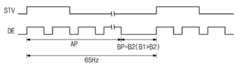
도 19를 참조하면, 제1 프레임(F1, 도 3에 도시됨)에서 현재 프레임의 영상 신호(RGBi)가 제2 영역(A2)에 표시될 영상이면, 테스트 영역 판별부(123)는 인에이블 신호(EN)를 활성 상태로 출력한다.Referring to FIG. 19, if the image signal RGBi of the current frame is an image to be displayed in the second area A2 in the first frame F1 (shown in FIG. 3 ), the test
제어 신호 발생부(124) 내 비교기(201, 도 18에 도시됨)는 인에이블 신호(EN)에 응답해서 현재 프레임의 영상 신호(RGBi)와 이전 프레임의 영상 신호(RGBi-1)를 제1 방향(D1)으로 쉬프트한 영상 신호를 비교한다. 만일, 현재 프레임의 영상 신호(RGBi)와 이전 프레임의 영상 신호(RGBi-1)를 제1 방향(D1)으로 쉬프트한 영상 신호가 일치하지 않으면, 비교기(201)는 하이 레벨의 주파수 변경 신호(VF)를 출력한다. 제어 신호 발생기(202)는 주파수 변경 신호(VF)가 하이 레벨인 동안 노말 주파수 레벨(예를 들면, 60Hz)의 수직 동기 시작 신호(STV)를 발생한다. 만일, 현재 프레임의 영상 신호(RGBi)와 이전 프레임의 영상 신호(RGBi-1)를 제1 방향(D1)으로 쉬프트한 영상 신호가 일치하면, 비교기(201)는 로우 레벨의 주파수 변경 신호(VF)를 출력한다. 제어 신호 발생기(202)는 주파수 변경 신호(VF)가 로우 레벨인 동안, 주파수가 변경 주파수 레벨(예를 들면, 65Hz) 및 노말 주파수 레벨(예를 들면, 60Hz)로 번갈아 변경되는 수직 동기 시작 신호(STV)를 발생한다. 변경 주파수 레벨은 휘도 차가 인지되지 않는 최적의 주파수 레벨로 설정되는 것이 바람직하며, 노말 주파수 레벨보다 높은 주파수 레벨 또는 낮은 주파수 레벨로 설정될 수 있다.The comparator 201 (shown in FIG. 18) in the
도 19에서는 이전 프레임의 영상 신호(RGBi-1)가 제1 영역(A1)에 표시된 신호이고, 현재 프레임의 영상 신호(RGBi)가 제2 영역(A2)에 표시될 신호인 것을 예시적으로 설명하였으나, 이전 프레임의 영상 신호(RGBi-1)가 제2 영역(A2)에 표시된 신호이고, 현재 프레임의 영상 신호(RGBi)가 제1 영역(A1)에 표시될 신호일 수 있다. 즉, 영상 신호(RGB)의 이동 방향이 제1 방향(D1) 뿐만 아니라 제1 방향(D1)과 일직선 상에서 역방향인 경우도 비교기(201)는 로우 레벨의 주파수 변경 신호(VF)를 출력한다. 또한 제1 영역(A1) 및 제2 영역(A2) 각각의 위치 및 크기는 영상의 특성을 고려하여 다양하게 변경 설정될 수 있다.FIG. 19 exemplarily illustrates that the image signal RGBi-1 of the previous frame is a signal displayed in the first area A1, and the image signal RGBi of the current frame is a signal to be displayed in the second area A2. However, the image signal RGBi-1 of the previous frame may be a signal displayed in the second area A2, and the image signal RGBi of the current frame may be a signal to be displayed in the first area A1. That is, when the moving direction of the image signal RGB is not only in the first direction D1 but also in the reverse direction in a straight line with the first direction D1, the
또한, 테스트 영역으로 사용되는 제1 영역(A1) 및 제2 영역(A2)의 크기는 표시 패널(110) 전체의 크기보다 작으므로 제어 신호 발생부(124)의 비교 연산에 사용되는 데이터 크기가 감소된다.Also, since the sizes of the first area A1 and the second area A2 used as the test area are smaller than the size of the
도 21 및 도 22은 도 18에 도시된 제어 신호 발생기에서 발생하는 수직 동기 시작 신호 및 출력 인에이블 신호의 타이밍도들이다.21 and 22 are timing diagrams of a vertical synchronization start signal and an output enable signal generated in the control signal generator shown in FIG. 18.
도 18 및 도 21을 참조하면, 제어 신호 발생기(202)는 주파수 변경 신호(VF)가 하이 레벨인 동안 제어 신호(CTRL)에 근거해서 노말 주파수 레벨(60Hz)의 수직 동기 시작 신호(STV)를 발생한다. 제어 신호 발생기(202)는 수직 동기 시작 신호(STV)에 동기해서 데이터 인에이블 신호(DE)를 발생한다.18 and 21, the
도 18 및 도 22를 참조하면, 제어 신호 발생기(202)는 주파수 변경 신호(VF)가 로우 레벨인 동안 제어 신호(CTRL)에 근거해서 주파수가 변경 주파수 레벨(65Hz) 및 노말 주파수 레벨(60Hz)로 번갈아 변경되는 수직 동기 시작 신호(STV)를 발생한다. 제어 신호 발생기(202)는 수직 동기 시작 신호(STV)에 동기해서 데이터 인에이블 신호(DE)를 발생한다.18 and 22, the
도 21 및 도 22의 비교에서 알 수 있는 바와 같이, 한 프레임 내에서 데이터 신호(DATA)가 표시 패널(110, 도 1에 도시됨)로 제공되는 액티브 구간(AP)은 수직 동기 시작 신호(STV)의 주파수와 무관에게 일정하다. 수직 동기 시작 신호(STV)의 주파수가 60Hz인 동안 한 프레임 내 블랭크 구간(BP=B1)은 수직 동기 시작 신호(STV)의 주파수가 65Hz인 동안 한 프레임 내 블랭크 구간(BP=B2)보다 길다(B1>B2). 즉, 수직 동기 시작 신호(STV)의 주파수가 높아짐에 따라서 블랭크 구간이 짧아진다. 이와 같이, 수직 동기 시작 신호(STV)의 주파수가 변경되더라도 한 프레임 내에서 데이터 신호(DATA)가 표시 패널(110, 도 1에 도시됨)로 제공되는 액티브 구간(AP)은 변경되지 않으므로 표시 영상의 품질은 저하되지 않으면서 킥백에 의한 휘도 차가 인지되는 것을 방지할 수 있다. As can be seen from the comparison of FIGS. 21 and 22, the active period AP in which the data signal DATA is provided to the display panel 110 (shown in FIG. 1) within one frame is the vertical synchronization start signal STV. ) Is constant regardless of the frequency. While the frequency of the vertical synchronization start signal (STV) is 60 Hz, the blank section (BP = B1) within one frame is longer than the blank section (BP = B2) in one frame while the frequency of the vertical synchronization start signal (STV) is 65 Hz ( B1>B2). That is, as the frequency of the vertical synchronization start signal STV increases, the blank section becomes shorter. In this way, even if the frequency of the vertical synchronization start signal STV is changed, the active period AP provided to the display panel 110 (shown in FIG. 1) of the data signal DATA within one frame is not changed. It is possible to prevent a difference in luminance due to kickback from being perceived without deteriorating the quality of.
즉, 수직 동기 시작 신호(STV)가 60Hz인 동안, 현재 프레임의 영상 신호(RGBi)가 이전 프레임의 영상 신호(RGBi-1)를 제1 방향(D1)으로 쉬프트한 영상 신호와 일치할 때 킥백에 의한 휘도 차가 인지되는 경우, 수직 동기 시작 신호(STV)의 주파수를 65Hz, 60Hz, 65Hz로 번갈아 변경하는 것에 의해서 사용자는 휘도 차를 인지하지 못한다.That is, while the vertical synchronization start signal (STV) is 60 Hz, the kickback is performed when the video signal RGBi of the current frame coincides with the video signal shifted from the previous frame RGBi-1 in the first direction D1. When the difference in luminance by is recognized, the user does not recognize the difference in luminance by alternately changing the frequency of the vertical synchronization start signal STV to 65Hz, 60Hz, and 65Hz.
마찬가지로, 수직 동기 시작 신호(STV)가 120Hz인 동안, 현재 프레임의 영상 신호(RGBi)가 이전 프레임의 영상 신호(RGBi-1)를 제1 방향(D1)으로 쉬프트한 영상 신호와 일치할 때 킥백에 의한 휘도 차가 인지되는 경우, 수직 동기 시작 신호(STV)의 주파수를 130Hz, 120Hz, 130Hz로 변경하는 것에 의해서 사용자는 휘도 차를 인지하지 못한다.Likewise, while the vertical synchronization start signal (STV) is 120Hz, kickback when the video signal (RGBi) of the current frame matches the video signal (RGBi-1) of the previous frame shifted in the first direction (D1). When the difference in luminance by is recognized, the user does not recognize the difference in luminance by changing the frequency of the vertical synchronization start signal STV to 130Hz, 120Hz, and 130Hz.
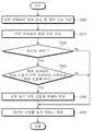
도 23은 본 발명의 실시예에 따른 표시 장치의 구동 방법을 보여주는 플로우차트이다. 설명의 편의를 위하여 도 16에 도시된 타이밍 컨트롤러를 참조하여 표시 장치의 구동 방법을 설명한다.23 is a flowchart illustrating a method of driving a display device according to an exemplary embodiment of the present invention. For convenience of explanation, a method of driving the display device will be described with reference to the timing controller illustrated in FIG. 16.
도 16 및 도 23을 참조하면, 타이밍 컨트롤러(120)는 현재 프레임의 영상 신호(RGBi)와 제어 신호(CTRL)를 수신한다(S300). 제어 신호 발생부(124)는 버퍼(122)로부터 이전 프레임의 영상 신호(RGBi-1)를 수신한다(S310).16 and 23, the
테스트 영역 판별부(123)는 제어 신호(CTRL)에 근거해서 현재 프레임의 영상 신호(RGBi)가 테스트 영역(A2, 도 19에 도시됨)에 표시될 영상 신호인 지를 판별한다(S320).The test
만일 현재 프레임의 영상 신호(RGBi)가 테스트 영역(A2)에 표시될 영상 신호이면, 제어 신호 발생부(124)는 현재 프레임의 영상 신호(RGBi)가 이전 프레임의 영상 신호(RGBi-1)를 제1 방향(D1)으로 소정 픽셀 쉬프트한 영상 신호와 일치하는 지의 여부를 판별한다(S330).If the image signal RGBi of the current frame is an image signal to be displayed in the test area A2, the
만일 현재 프레임의 영상 신호(RGBi)가 이전 프레임의 영상 신호(RGBi-1)를 제1 방향(D1)으로 소정 픽셀 쉬프트한 영상 신호와 일치하면, 제어 신호 발생부(124)는 수직 동기 시작 신호(STV)의 주파수를 변경한다(S340). 제어 신호 발생부(124)는 수직 동기 시작 신호(STV)에 동기해서 출력 인에이블 신호(DE)를 출력한다. 제어 신호 발생부(124)는 제어 신호(CTRL)에 근거해서 수평 동기 시작 신호(STH), 클럭 신호(HCLK) 및 라인 래치 신호(TP)를 데이터 드라이버(140, 도 1에 도시됨)로 제공하고, 수직 동기 시작 신호(STV) 및 출력 인에이블 신호(DE)를 게이트 드라이버(130)로 제공한다.If the image signal RGBi of the current frame coincides with the image signal obtained by shifting the image signal RGBi-1 of the previous frame by a predetermined pixel in the first direction D1, the
영상 처리부(121)는 영상 신호(RGB)에 대한 영상 처리를 수행한 데이터 신호(DATA)를 데이터 드라이버(140, 도 1에 도시됨)로 제공한다.The
도 2 및 도 8에 도시된 표시 패널(110)은 하나의 픽셀(PX)이 3개의 서브 픽셀들 즉, 레드 서브 픽셀, 그린 서브 픽셀 및 블루 서브 픽셀을 포함하는 것을 일 예로 도시하고 설명한다. 그러나, 표시 패널(110)은 하나의 픽셀(PX)이 6 개의 서브 픽셀들 즉, 레드 서브 픽셀 2개, 그린 서브 픽셀 2개 및 블루 서브 픽셀 2개를 포함하는 SPVA(Super Patterned Vertical Alignment) 모드로 구현될 수 있다.The
즉, 표시 패널이 어떠한 타입이더라도 반전 구동되는 표시 패널에서 영상이 매 프레임마다 소정 픽셀씩 이동함에 따라서 서브 픽셀들 간 휘도 차가 발생하는 표시 장치에 본 발명이 적용될 수 있다.That is, no matter what type of display panel, the present invention can be applied to a display device in which a luminance difference between sub-pixels occurs as an image moves by a predetermined pixel every frame in a display panel that is driven inversion.
예시적인 바람직한 실시예들을 이용하여 본 발명을 설명하였지만, 본 발명의 범위는 개시된 실시예들에 한정되지 않는다는 것이 잘 이해될 것이다. 오히려, 본 발명의 범위에는 다양한 변형 예들 및 그 유사한 구성들이 모두 포함될 수 있도록 하려는 것이다. 따라서, 청구범위는 그러한 변형 예들 및 그 유사한 구성들 모두를 포함하는 것으로 가능한 폭넓게 해석되어야 한다.While the present invention has been described using exemplary preferred embodiments, it will be understood that the scope of the invention is not limited to the disclosed embodiments. Rather, it is intended that various modifications and similar configurations may be included in the scope of the present invention. Accordingly, the claims are to be interpreted as broadly as possible as including all such variations and similar configurations.
100: 표시 장치110: 표시 패널
120: 타이밍 컨트롤러121: 영상 처리부
122; 버퍼123: 테스트 영역 판별부
124: 제어 신호 발생부130: 게이트 드라이버
140: 데이트 드라이버160: 킥백 검출기
170: 감마 전압 발생기201: 비교기
202: 제어 신호 발생기100: display device 110: display panel
120: timing controller 121: image processing unit
122; Buffer 123: test area determination unit
124: control signal generator 130: gate driver
140: date driver 160: kickback detector
170: gamma voltage generator 201: comparator
202: control signal generator
Claims (19)
Translated fromKorean상기 복수의 데이터 라인들을 구동하는 데이터 드라이버와;
수직 동기 시작 신호에 동기해서 상기 복수의 게이트 라인들을 구동하는 게이트 드라이버; 및
외부로부터 입력된 영상 신호 및 제어 신호에 응답해서 상기 데이터 드라이버 및 상기 게이트 드라이버를 제어하고, 상기 게이트 드라이버로 제공하기 위한 상기 수직 동기 시작 신호를 출력하는 타이밍 컨트롤러를 포함하되,
상기 타이밍 컨트롤러는 현재 프레임의 영상 신호가 이전 프레임의 영상 신호를 제1 방향으로 쉬프트한 영상 신호와 일치할 때 상기 수직 동기 시작 신호의 주파수를 변경 주파수 레벨 및 노말 주파수 레벨로 번갈아 변경하는 것을 특징으로 하는 표시 장치.A display panel including a plurality of data lines and a plurality of pixels respectively connected to the plurality of gate lines;
A data driver driving the plurality of data lines;
A gate driver driving the plurality of gate lines in synchronization with a vertical synchronization start signal; And
A timing controller that controls the data driver and the gate driver in response to an image signal and a control signal input from the outside, and outputs the vertical synchronization start signal to be provided to the gate driver,
The timing controller alternately changes the frequency of the vertical synchronization start signal to a change frequency level and a normal frequency level when the video signal of the current frame coincides with the video signal shifting the video signal of the previous frame in the first direction. Display device.
상기 타이밍 컨트롤러는,
상기 수직 동기 시작 신호에 동기해서 상기 게이트 드라이버로 제공하기 위한 데이터 인에이블 신호를 더 출력하되,
상기 데이터 인에이블 신호는 액티브 구간과 블랭크 구간을 포함하는 것을 특징으로 하는 표시 장치.The method of claim 1,
The timing controller,
In synchronization with the vertical synchronization start signal, a data enable signal to be provided to the gate driver is further output,
The display device according to claim 1, wherein the data enable signal includes an active period and a blank period.
상기 데이터 인에이블 신호의 상기 블랭크 구간은 상기 수직 동기 시작 신호의 주파수에 반비례하는 것을 특징으로 하는 표시 장치.The method of claim 2,
The display device, wherein the blank period of the data enable signal is in inverse proportion to the frequency of the vertical synchronization start signal.
상기 타이밍 컨트롤러는,
상기 데이터 인에이블 신호에 동기해서 상기 데이터 드라이버로 제공하기 위한 수평 동기 시작 신호를 더 출력하는 것을 특징으로 하는 표시 장치.The method of claim 2,
The timing controller,
And further outputting a horizontal synchronization start signal to be provided to the data driver in synchronization with the data enable signal.
상기 타이밍 컨트롤러는,
상기 현재 프레임의 영상 신호가 상기 이전 프레임의 영상 신호를 상기 제1 방향으로 H(H는 양의 정수) 픽셀만큼 쉬프트한 영상 신호와 일치할 때 상기 수직 동기 시작 신호의 주파수를 변경하는 것을 특징으로 하는 표시 장치.The method of claim 1,
The timing controller,
The frequency of the vertical synchronization start signal is changed when the video signal of the current frame coincides with the video signal shifted by H (H is a positive integer) pixels in the first direction of the video signal of the previous frame. Display device.
상기 타이밍 컨트롤러는,
노말 모드에서 상기 수직 동기 시작 신호의 주파수가 60Hz일 때 상기 현재 프레임의 영상 신호가 상기 이전 프레임의 영상 신호를 상기 제1 방향으로 1 픽셀만큼 쉬프트한 영상 신호와 일치할 때 상기 수직 동기 시작 신호의 주파수를 변경하는 것을 특징으로 하는 표시 장치.The method of claim 5,
The timing controller,
In the normal mode, when the frequency of the vertical synchronization start signal is 60 Hz, when the video signal of the current frame matches the video signal of the previous frame by one pixel in the first direction, the vertical synchronization start signal A display device, characterized in that the frequency is changed.
상기 타이밍 컨트롤러는,
노말 모드에서 상기 수직 동기 시작 신호의 주파수가 120Hz일 때 상기 현재 프레임의 영상 신호가 이전 프레임의 영상 신호를 상기 제1 방향으로 2 픽셀만큼 쉬프트한 영상 신호와 일치할 때 상기 수직 동기 시작 신호의 주파수를 변경하는 것을 특징으로 하는 표시 장치.The method of claim 5,
The timing controller,
In normal mode, when the frequency of the vertical synchronization start signal is 120 Hz, the frequency of the vertical synchronization start signal when the video signal of the current frame matches the video signal of the previous frame by 2 pixels shifted in the first direction. The display device, characterized in that to change.
상기 타이밍 컨트롤러는,
상기 영상 신호를 데이터 신호로 변환해서 상기 데이터 드라이버로 제공하는 영상 처리부와;
상기 영상 신호를 저장하고, 상기 이전 프레임의 영상 신호를 출력하는 버퍼와;
상기 제어 신호를 수신하고, 상기 영상 신호가 상기 표시 패널의 테스트 영역 내에 표시될 영상 신호인 지의 여부를 판별하고, 판별 결과에 대응하는 인에이블 신호를 출력하는 테스트 영역 판별부와;
상기 영상 신호를 상기 현재 프레임의 영상 신호로 수신하고, 상기 버퍼로부터의 상기 이전 프레임의 영상 신호를 수신하고, 상기 제어 신호 및 상기 인에이블 신호에 응답해서 상기 수직 동기 시작 신호를 출력하는 제어 신호 발생부를 포함하는 것을 특징으로 하는 표시 장치.The method of claim 1,
The timing controller,
An image processing unit converting the image signal into a data signal and providing it to the data driver;
A buffer storing the video signal and outputting the video signal of the previous frame;
A test area determining unit receiving the control signal, determining whether the image signal is an image signal to be displayed in a test area of the display panel, and outputting an enable signal corresponding to a result of the determination;
Generating a control signal for receiving the video signal as the video signal of the current frame, receiving the video signal of the previous frame from the buffer, and outputting the vertical synchronization start signal in response to the control signal and the enable signal A display device comprising a unit.
상기 제어 신호 발생부는,
상기 인에이블 신호가 활성 상태일 때 상기 현재 프레임의 영상 신호와 상기 이전 프레임의 영상 신호를 제1 방향으로 쉬프트한 영상 신호를 비교하고, 주파수 변경 신호를 출력하는 비교기; 및
상기 주파수 변경 신호 및 상기 제어 신호에 응답해서 상기 수직 동기 시작 신호를 출력하는 제어 신호 발생부를 포함하는 것을 특징으로 하는 표시 장치.The method of claim 8,
The control signal generator,
A comparator for comparing an image signal obtained by shifting the image signal of the current frame and the image signal of the previous frame in a first direction when the enable signal is active, and outputting a frequency change signal; And
And a control signal generator configured to output the vertical synchronization start signal in response to the frequency change signal and the control signal.
상기 제어 신호 발생부는,
상기 수직 동기 시작 신호에 동기해서 상기 게이트 드라이버로 제공하기 위한 데이터 인에이블 신호를 더 출력하되,
상기 데이터 인에이블 신호는 액티브 구간과 블랭크 구간을 포함하는 것을 특징으로 하는 표시 장치.The method of claim 9,
The control signal generator,
In synchronization with the vertical synchronization start signal, a data enable signal to be provided to the gate driver is further output,
The display device according to claim 1, wherein the data enable signal includes an active period and a blank period.
상기 데이터 인에이블 신호의 상기 블랭크 구간은 상기 수직 동기 시작 신호의 주파수에 반비례하는 것을 특징으로 하는 표시 장치.The method of claim 10,
The display device, wherein the blank period of the data enable signal is in inverse proportion to the frequency of the vertical synchronization start signal.
상기 제어 신호 발생부는,
상기 데이터 인에이블 신호에 동기해서 상기 데이터 드라이버로 제공하기 위한 수평 동기 시작 신호를 더 출력하는 것을 특징으로 하는 표시 장치.The method of claim 11,
The control signal generator,
And further outputting a horizontal synchronization start signal to be provided to the data driver in synchronization with the data enable signal.
상기 제어 신호 발생부는,
상기 현재 프레임의 영상 신호가 이전 프레임의 영상 신호를 상기 제1 방향으로 H(H는 양의 정수) 픽셀만큼 쉬프트한 영상 신호와 일치할 때 상기 수직 동기 시작 신호의 주파수를 변경하는 것을 특징으로 하는 표시 장치.The method of claim 10,
The control signal generator,
The frequency of the vertical synchronization start signal is changed when the video signal of the current frame coincides with the video signal shifted by H (H is a positive integer) pixels in the first direction of the video signal of the previous frame. Display device.
상기 제어 신호 발생부는,
노말 모드에서 상기 수직 동기 시작 신호의 주파수가 60Hz일 때 상기 현재 프레임의 영상 신호가 이전 프레임의 영상 신호를 상기 제1 방향으로 1 픽셀만큼 쉬프트한 영상 신호와 일치할 때 상기 수직 동기 시작 신호의 주파수를 변경하는 것을 특징으로 하는 표시 장치.The method of claim 10,
The control signal generator,
In normal mode, when the frequency of the vertical synchronization start signal is 60 Hz, the frequency of the vertical synchronization start signal when the video signal of the current frame matches the video signal of the previous frame by one pixel shifted in the first direction. The display device, characterized in that to change.
버퍼로부터 이전 프레임의 영상 신호를 수신하는 단계와;
수직 동기 시작 신호를 발생하는 단계와;
상기 현재 프레임의 영상 신호가 상기 이전 프레임의 영상 신호를 제1 방향으로 쉬프트한 영상 신호와 일치할 때 상기 수직 동기 시작 신호의 주파수를 변경 주파수 레벨 및 노말 주파수 레벨로 번갈아 변경하는 단계; 및
상기 수직 동기 시작 신호에 동기해서 상기 현재 프레임의 영상 신호 대응하는 데이터 신호를 표시 패널로 제공하는 단계를 포함하는 것을 특징으로 하는 표시 장치의 구동 방법.Receiving an image signal and a control signal of the current frame;
Receiving a video signal of a previous frame from a buffer;
Generating a vertical synchronization start signal;
Alternately changing the frequency of the vertical synchronization start signal to a change frequency level and a normal frequency level when the video signal of the current frame coincides with the video signal shifted in the first direction of the video signal of the previous frame; And
And providing a data signal corresponding to the video signal of the current frame to a display panel in synchronization with the vertical synchronization start signal.
상기 수직 동기 시작 신호에 동기해서 액티브 구간과 블랭크 구간을 포함하는 데이터 인에이블 신호를 발생하는 단계를 더 포함하는 것을 특징으로 하는 표시 장치의 구동 방법.The method of claim 15,
And generating a data enable signal including an active period and a blank period in synchronization with the vertical synchronization start signal.
상기 데이터 인에이블 신호의 상기 블랭크 구간은 상기 수직 동기 시작 신호의 주파수에 반비례하는 것을 특징으로 하는 표시 장치의 구동 방법.The method of claim 16,
And the blank period of the data enable signal is in inverse proportion to the frequency of the vertical synchronization start signal.
상기 주파수 변경 단계는,
상기 현재 프레임의 영상 신호가 상기 이전 프레임의 영상 신호를 상기 제1 방향으로 H(H는 양의 정수) 픽셀만큼 쉬프트한 영상 신호와 일치할 때 상기 수직 동기 시작 신호의 주파수를 변경하는 단계를 포함하는 것을 특징으로 하는 표시 장치의 구동 방법.The method of claim 15,
The frequency changing step,
Changing the frequency of the vertical synchronization start signal when the video signal of the current frame coincides with the video signal shifted by H (H is a positive integer) pixels in the first direction of the video signal of the previous frame A driving method of a display device, comprising: a.
상기 현재 프레임의 영상 신호가 테스트 영역에 표시될 영상 신호일 때 인에이블 신호를 활성화하는 단계를 더 포함하며,
상기 인에이블 신호가 활성 상태일 때 상기 주파수 변경 단계를 수행하는 것을 특징으로 하는 표시 장치의 구동 방법.
The method of claim 15,
The step of activating an enable signal when the video signal of the current frame is a video signal to be displayed in the test area,
And performing the frequency change step when the enable signal is active.
Priority Applications (2)
| Application Number | Priority Date | Filing Date | Title |
|---|---|---|---|
| KR1020140006822AKR102198250B1 (en) | 2014-01-20 | 2014-01-20 | Display apparatus and driving method thereof |
| US14/457,551US9646555B2 (en) | 2014-01-20 | 2014-08-12 | Display device in which frequency of vertical sync start signal is selectively changed and method of driving the same |
Applications Claiming Priority (1)
| Application Number | Priority Date | Filing Date | Title |
|---|---|---|---|
| KR1020140006822AKR102198250B1 (en) | 2014-01-20 | 2014-01-20 | Display apparatus and driving method thereof |
Publications (2)
| Publication Number | Publication Date |
|---|---|
| KR20150086772A KR20150086772A (en) | 2015-07-29 |
| KR102198250B1true KR102198250B1 (en) | 2021-01-05 |
Family
ID=53545313
Family Applications (1)
| Application Number | Title | Priority Date | Filing Date |
|---|---|---|---|
| KR1020140006822AExpired - Fee RelatedKR102198250B1 (en) | 2014-01-20 | 2014-01-20 | Display apparatus and driving method thereof |
Country Status (2)
| Country | Link |
|---|---|
| US (1) | US9646555B2 (en) |
| KR (1) | KR102198250B1 (en) |
Families Citing this family (6)
| Publication number | Priority date | Publication date | Assignee | Title |
|---|---|---|---|---|
| CN104808407B (en)* | 2015-05-07 | 2018-05-01 | 深圳市华星光电技术有限公司 | TFT array substrate |
| KR102554967B1 (en)* | 2016-10-31 | 2023-07-13 | 삼성디스플레이 주식회사 | Display device capable of changing frame rate and driving method thereof |
| KR102581307B1 (en)* | 2018-01-03 | 2023-09-22 | 삼성디스플레이 주식회사 | Display device and electronic device having the same |
| CN111312149B (en)* | 2020-03-10 | 2023-12-08 | Tcl华星光电技术有限公司 | Driving method and driving device |
| CN111477152B (en)* | 2020-05-06 | 2021-11-02 | Tcl华星光电技术有限公司 | Time sequence controller, time sequence control method and storage medium |
| KR20240108920A (en)* | 2023-01-02 | 2024-07-10 | 삼성디스플레이 주식회사 | Display device, display system, and method of driving the same |
Citations (1)
| Publication number | Priority date | Publication date | Assignee | Title |
|---|---|---|---|---|
| US20030142054A1 (en)* | 2002-01-31 | 2003-07-31 | Norio Tada | Flat-panel display device |
Family Cites Families (23)
| Publication number | Priority date | Publication date | Assignee | Title |
|---|---|---|---|---|
| JP3487259B2 (en) | 2000-05-22 | 2004-01-13 | 日本電気株式会社 | Video display device and display method thereof |
| JP2004163829A (en) | 2002-11-15 | 2004-06-10 | Sharp Corp | Liquid crystal display |
| KR101034943B1 (en) | 2003-12-10 | 2011-05-17 | 엘지디스플레이 주식회사 | LCD and its driving method |
| KR20060018393A (en) | 2004-08-24 | 2006-03-02 | 삼성전자주식회사 | Display device |
| KR100609056B1 (en) | 2004-12-01 | 2006-08-09 | 삼성전자주식회사 | Display device and control method |
| JP4687322B2 (en)* | 2005-08-12 | 2011-05-25 | カシオ計算機株式会社 | Imaging device |
| KR100804923B1 (en)* | 2005-08-12 | 2008-02-20 | 가시오게산키 가부시키가이샤 | Timing signal processing device and camera device for controlling driving of image pickup device |
| TWI275058B (en)* | 2005-11-10 | 2007-03-01 | Ind Tech Res Inst | Display apparatus with dynamic scanning backlight and control method and device thereof |
| KR101255701B1 (en)* | 2006-06-27 | 2013-04-17 | 엘지디스플레이 주식회사 | Appratus and method for driving LCD |
| TWI341504B (en) | 2006-11-10 | 2011-05-01 | Chimei Innolux Corp | Liquid crystal display device and method for driving the same |
| KR20080048655A (en)* | 2006-11-29 | 2008-06-03 | 엘지디스플레이 주식회사 | Driving apparatus and driving method of liquid crystal display |
| KR20080050032A (en)* | 2006-12-01 | 2008-06-05 | 삼성전자주식회사 | Display device and driving method |
| KR101276663B1 (en) | 2007-02-28 | 2013-06-19 | 엘지디스플레이 주식회사 | Driving circuit unit for LCD |
| KR101222987B1 (en) | 2007-05-11 | 2013-01-17 | 엘지디스플레이 주식회사 | Liquid Crystal Display and Driving Method thereof |
| KR20080110232A (en)* | 2007-06-15 | 2008-12-18 | 엘지디스플레이 주식회사 | LCD and its driving method |
| KR101329706B1 (en)* | 2007-10-10 | 2013-11-14 | 엘지디스플레이 주식회사 | liquid crystal display device and driving method of the same |
| KR101452972B1 (en)* | 2008-02-13 | 2014-10-22 | 삼성디스플레이 주식회사 | Timing controller, display appartus having the same and signal processing method of the same |
| JP4643727B2 (en)* | 2009-05-29 | 2011-03-02 | 株式会社東芝 | Image processing apparatus and image processing method |
| KR101598396B1 (en)* | 2009-11-27 | 2016-03-15 | 삼성디스플레이 주식회사 | Method for displaying stereo-scopic image and display apparatus for performing the same |
| JP5469552B2 (en) | 2010-07-08 | 2014-04-16 | シャープ株式会社 | Liquid crystal display |
| KR20120070921A (en) | 2010-12-22 | 2012-07-02 | 엘지디스플레이 주식회사 | Timing controller and organic light emitting diode display using the same |
| US9208736B2 (en) | 2011-11-28 | 2015-12-08 | Samsung Display Co., Ltd. | Display device and driving method thereof |
| KR101350737B1 (en)* | 2012-02-20 | 2014-01-14 | 엘지디스플레이 주식회사 | Timing controller and liquid crystal display device comprising the same |
- 2014
- 2014-01-20KRKR1020140006822Apatent/KR102198250B1/ennot_activeExpired - Fee Related
- 2014-08-12USUS14/457,551patent/US9646555B2/enactiveActive
Patent Citations (1)
| Publication number | Priority date | Publication date | Assignee | Title |
|---|---|---|---|---|
| US20030142054A1 (en)* | 2002-01-31 | 2003-07-31 | Norio Tada | Flat-panel display device |
Also Published As
| Publication number | Publication date |
|---|---|
| KR20150086772A (en) | 2015-07-29 |
| US9646555B2 (en) | 2017-05-09 |
| US20150206489A1 (en) | 2015-07-23 |
Similar Documents
| Publication | Publication Date | Title |
|---|---|---|
| US8970564B2 (en) | Apparatus and method for driving liquid crystal display | |
| US8384708B2 (en) | Apparatus and method for dividing liquid crystal display device | |
| KR101243811B1 (en) | A liquid crystal display device and a method for driving the same | |
| KR101563265B1 (en) | Display device and method for driving the same | |
| KR101399017B1 (en) | Display apparatus and method of driving the same | |
| US9978302B2 (en) | Liquid crystal display | |
| US20140320478A1 (en) | Display Device For Low Speed Drive And Method For Driving The Same | |
| KR102198250B1 (en) | Display apparatus and driving method thereof | |
| KR102099281B1 (en) | Liquid crystal display and method for driving the same | |
| KR102147055B1 (en) | Liquid display device and driving method for the same | |
| KR20080054658A (en) | Driving device of liquid crystal display and driving method thereof | |
| US10726767B2 (en) | Display apparatus and method of driving the same | |
| KR102338944B1 (en) | Liquid crystal display device and method for driving the same | |
| KR20150076442A (en) | Liquid crystal display | |
| JP4896961B2 (en) | Liquid crystal panel driving device, liquid crystal panel driving method, and liquid crystal display device | |
| US9064467B2 (en) | Liquid crystal display device and driving method thereof | |
| KR20130028596A (en) | Method of controling dot inversion for lcd device | |
| KR20040049558A (en) | Liquid crystal display and method of driving the same | |
| KR20080049464A (en) | LCD and its driving method | |
| KR101649233B1 (en) | Method for processing data of liquid crystal display using MEMC chip | |
| KR20100033893A (en) | Liquid crystal display device and driving method thereof | |
| KR20160094513A (en) | Display Panel for Display Device | |
| KR20070079103A (en) | LCD and its driving method | |
| KR20130018025A (en) | Signal processing unit and liquid crystal display device comprising the same | |
| KR20110071967A (en) | Driving device of liquid crystal display and driving method thereof |
Legal Events
| Date | Code | Title | Description |
|---|---|---|---|
| PA0109 | Patent application | St.27 status event code:A-0-1-A10-A12-nap-PA0109 | |
| R17-X000 | Change to representative recorded | St.27 status event code:A-3-3-R10-R17-oth-X000 | |
| PG1501 | Laying open of application | St.27 status event code:A-1-1-Q10-Q12-nap-PG1501 | |
| R18-X000 | Changes to party contact information recorded | St.27 status event code:A-3-3-R10-R18-oth-X000 | |
| A201 | Request for examination | ||
| PA0201 | Request for examination | St.27 status event code:A-1-2-D10-D11-exm-PA0201 | |
| R18-X000 | Changes to party contact information recorded | St.27 status event code:A-3-3-R10-R18-oth-X000 | |
| E902 | Notification of reason for refusal | ||
| PE0902 | Notice of grounds for rejection | St.27 status event code:A-1-2-D10-D21-exm-PE0902 | |
| P11-X000 | Amendment of application requested | St.27 status event code:A-2-2-P10-P11-nap-X000 | |
| P13-X000 | Application amended | St.27 status event code:A-2-2-P10-P13-nap-X000 | |
| E701 | Decision to grant or registration of patent right | ||
| PE0701 | Decision of registration | St.27 status event code:A-1-2-D10-D22-exm-PE0701 | |
| GRNT | Written decision to grant | ||
| PR0701 | Registration of establishment | St.27 status event code:A-2-4-F10-F11-exm-PR0701 | |
| PR1002 | Payment of registration fee | St.27 status event code:A-2-2-U10-U11-oth-PR1002 Fee payment year number:1 | |
| PG1601 | Publication of registration | St.27 status event code:A-4-4-Q10-Q13-nap-PG1601 | |
| PC1903 | Unpaid annual fee | St.27 status event code:A-4-4-U10-U13-oth-PC1903 Not in force date:20231229 Payment event data comment text:Termination Category : DEFAULT_OF_REGISTRATION_FEE | |
| PC1903 | Unpaid annual fee | St.27 status event code:N-4-6-H10-H13-oth-PC1903 Ip right cessation event data comment text:Termination Category : DEFAULT_OF_REGISTRATION_FEE Not in force date:20231229 |