KR102197826B1 - Display device - Google Patents
Display deviceDownload PDFInfo
- Publication number
- KR102197826B1 KR102197826B1KR1020140116991AKR20140116991AKR102197826B1KR 102197826 B1KR102197826 B1KR 102197826B1KR 1020140116991 AKR1020140116991 AKR 1020140116991AKR 20140116991 AKR20140116991 AKR 20140116991AKR 102197826 B1KR102197826 B1KR 102197826B1
- Authority
- KR
- South Korea
- Prior art keywords
- substrate
- polarizing plate
- sealing material
- protrusion
- light shielding
- Prior art date
- Legal status (The legal status is an assumption and is not a legal conclusion. Google has not performed a legal analysis and makes no representation as to the accuracy of the status listed.)
- Active
Links
Images


Classifications
- G—PHYSICS
- G02—OPTICS
- G02F—OPTICAL DEVICES OR ARRANGEMENTS FOR THE CONTROL OF LIGHT BY MODIFICATION OF THE OPTICAL PROPERTIES OF THE MEDIA OF THE ELEMENTS INVOLVED THEREIN; NON-LINEAR OPTICS; FREQUENCY-CHANGING OF LIGHT; OPTICAL LOGIC ELEMENTS; OPTICAL ANALOGUE/DIGITAL CONVERTERS
- G02F1/00—Devices or arrangements for the control of the intensity, colour, phase, polarisation or direction of light arriving from an independent light source, e.g. switching, gating or modulating; Non-linear optics
- G02F1/01—Devices or arrangements for the control of the intensity, colour, phase, polarisation or direction of light arriving from an independent light source, e.g. switching, gating or modulating; Non-linear optics for the control of the intensity, phase, polarisation or colour
- G02F1/13—Devices or arrangements for the control of the intensity, colour, phase, polarisation or direction of light arriving from an independent light source, e.g. switching, gating or modulating; Non-linear optics for the control of the intensity, phase, polarisation or colour based on liquid crystals, e.g. single liquid crystal display cells
- G02F1/133—Constructional arrangements; Operation of liquid crystal cells; Circuit arrangements
- G02F1/1333—Constructional arrangements; Manufacturing methods
- G02F1/1335—Structural association of cells with optical devices, e.g. polarisers or reflectors
- G02F1/133528—Polarisers
- G—PHYSICS
- G02—OPTICS
- G02F—OPTICAL DEVICES OR ARRANGEMENTS FOR THE CONTROL OF LIGHT BY MODIFICATION OF THE OPTICAL PROPERTIES OF THE MEDIA OF THE ELEMENTS INVOLVED THEREIN; NON-LINEAR OPTICS; FREQUENCY-CHANGING OF LIGHT; OPTICAL LOGIC ELEMENTS; OPTICAL ANALOGUE/DIGITAL CONVERTERS
- G02F1/00—Devices or arrangements for the control of the intensity, colour, phase, polarisation or direction of light arriving from an independent light source, e.g. switching, gating or modulating; Non-linear optics
- G02F1/01—Devices or arrangements for the control of the intensity, colour, phase, polarisation or direction of light arriving from an independent light source, e.g. switching, gating or modulating; Non-linear optics for the control of the intensity, phase, polarisation or colour
- G02F1/13—Devices or arrangements for the control of the intensity, colour, phase, polarisation or direction of light arriving from an independent light source, e.g. switching, gating or modulating; Non-linear optics for the control of the intensity, phase, polarisation or colour based on liquid crystals, e.g. single liquid crystal display cells
- G02F1/133—Constructional arrangements; Operation of liquid crystal cells; Circuit arrangements
- G02F1/1333—Constructional arrangements; Manufacturing methods
- G02F1/1339—Gaskets; Spacers; Sealing of cells
Landscapes
- Physics & Mathematics (AREA)
- Nonlinear Science (AREA)
- Mathematical Physics (AREA)
- Chemical & Material Sciences (AREA)
- Crystallography & Structural Chemistry (AREA)
- General Physics & Mathematics (AREA)
- Optics & Photonics (AREA)
- Liquid Crystal (AREA)
- Devices For Indicating Variable Information By Combining Individual Elements (AREA)
Abstract
Translated fromKoreanDescription
Translated fromKorean본 발명은 표시장치에 관한 것으로, 특히 표시패널의 측면에서 발생되는 빛샘 현상을 최소화할 수 있는 표시장치에 대한 것이다.The present invention relates to a display device, and more particularly, to a display device capable of minimizing a light leakage phenomenon occurring from a side of a display panel.
액정표시장치는 현재 가장 널리 사용되고 있는 평판 표시 장치 중 하나로서, 화소전극과 공통전극 등 전기장 생성 전극(field generating electrode)이 형성되어 있는 두 장의 기판과 그 사이에 들어 있는 액정층을 포함한다. 액정표시장치는 전기장 생성 전극에 전압을 인가하여 액정층의 액정 분자들을 재배열시켜 투과되는 빛의 양을 조절한다.A liquid crystal display is one of the most widely used flat panel displays, and includes two substrates on which field generating electrodes such as a pixel electrode and a common electrode are formed, and a liquid crystal layer interposed therebetween. In the liquid crystal display, a voltage is applied to an electric field generating electrode to rearrange liquid crystal molecules in a liquid crystal layer to control the amount of transmitted light.
일반적으로, 액정표시장치는 표시패널 및 이 표시패널로 광을 제공하는 백라이트 유닛을 포함한다.In general, a liquid crystal display device includes a display panel and a backlight unit providing light to the display panel.
표시패널은 액정층을 사이에 두고 합착된 상부 기판 및 하부 기판으로 구성된다.The display panel is composed of an upper substrate and a lower substrate bonded with a liquid crystal layer therebetween.
백라이트 유닛으로부터 표시패널로 광이 공급될 때 표시패널의 측면으로 빛이 새는 문제점이 있어 이 표시패널의 측면에 차광 시일재가 도포된다.When light is supplied from the backlight unit to the display panel, there is a problem in that light leaks to the side of the display panel, and a light shielding sealant is applied to the side of the display panel.
그러나, 종래의 차광 시일재는 그 두께가 균일하지 못하여 다음과 같은 문제점을 유발한다. 즉, 종래의 차광 시일재의 중심부의 두께는 두꺼운 반면, 이의 양 가장자리의 두께는 얇다. 이로 인해, 이의 양 가장자리에서 여전히 광이 투과되는 문제점이 있다.However, the conventional light-shielding sealing material is not uniform in thickness, causing the following problems. That is, the thickness of the center portion of the conventional light shielding sealing material is thick, while the thickness of both edges thereof is thin. For this reason, there is a problem in that light is still transmitted at both edges thereof.
본 발명은 상기와 같은 문제점을 해결하기 위하여 안출된 것으로, 표시패널의 측면으로부터 광이 새는 것을 최소화할 수 있는 표시장치를 제공하는데 그 목적이 있다.The present invention has been conceived to solve the above problems, and an object of the present invention is to provide a display device capable of minimizing light leakage from a side surface of a display panel.
상기와 같은 목적을 달성하기 위한 본 발명에 따른 표시장치는, 표시 영역과 비표시 영역을 갖는 제 1 기판; 제 1 기판과 대향하여 위치한 제 2 기판; 제 1 기판 및 제 2 기판의 적어도 하나의 측면 상에 위치한 차광 시일재; 및 제 1 기판 및 제 2 기판 중 적어도 하나의 면 상에 위치한 제 1 편광판을 포함하며; 제 1 편광판은 적어도 하나의 측면에서 연장된 가상의 연장면과 교차한다.In order to achieve the above object, a display device according to the present invention includes: a first substrate having a display area and a non-display area; A second substrate positioned opposite the first substrate; A light shielding material positioned on at least one side surface of the first substrate and the second substrate; And a first polarizing plate positioned on at least one of the first substrate and the second substrate; The first polarizing plate intersects a virtual extension surface extending from at least one side surface.
차광 시일재는 제 1 편광판의 측면 및 하면 중 적어도 하나와 접촉한다.The light shielding sealing material is in contact with at least one of a side surface and a lower surface of the first polarizing plate.
제 1 편광판의 단부와 측면 사이의 거리는 1um 내지 500um이다.The distance between the end and the side surface of the first polarizing plate is 1um to 500um.
제 1 기판 및 제 2 기판 중 다른 하나의 면 상에 위치한 제 2 편광판이 더 포함된다.A second polarizing plate positioned on the other surface of the first substrate and the second substrate is further included.
제 2 편광판은 적어도 하나의 측면에서 연장된 가상의 연장면과 교차한다.The second polarizing plate intersects a virtual extension surface extending from at least one side surface.
차광 시일재는 제 2 편광판의 측면 및 하면 중 적어도 하나와 접촉한다.The light shielding sealing material is in contact with at least one of a side surface and a lower surface of the second polarizing plate.
제 2 편광판의 단부와 측면 사이의 거리는 1um 내지 500um이다.The distance between the end and the side of the second polarizing plate is 1um to 500um.
제 1 편광판의 단부와 제 2 편광판의 단부가 동일 면상에 위치한다.The end of the first polarizing plate and the end of the second polarizing plate are positioned on the same plane.
본 발명에 따른 표시장치에 따르면 편광판이 기판보다 외곽으로 더 돌출되어 있다. 따라서, 차광 시일재가 도포될 때 이의 가장자리가 편광판의 돌출부 상에 올려질 수 있다. 이에 따라 차광 시일재의 가장자리에서의 빛샘 현상이 최소화 될 수 있다.According to the display device according to the present invention, the polarizing plate protrudes further outward than the substrate. Accordingly, when the light shielding sealing material is applied, its edge can be raised on the protrusion of the polarizing plate. Accordingly, light leakage at the edge of the light-shielding sealant can be minimized.
도 1은 본 발명의 한 실시예에 따른 표시장치를 나타낸 도면이다.
도 2는 도 1의 표시 영역에 위치한 화소들의 배열을 나타낸 도면이다.
도 3은 도 1의 I-I`의 선을 따라 자른 단면도이다.
도 4는 도 1의 I-I`의 선을 따라 자른 단면도에 대한 다른 실시예를 나타낸 도면이다.
도 5는 도 1의 I-I`의 선을 따라 자른 단면도에 대한 또 다른 실시예를 나타낸 도면이다.
도 6은 도 1의 II-II`의 선을 따라 자른 단면도이다.
도 7 내지 9는 돌출부의 길이와 양 기판의 측면들로부터의 광 투과율 간의 상관 관계를 설명하기 위한 도면이다.1 is a diagram illustrating a display device according to an exemplary embodiment of the present invention.
FIG. 2 is a diagram illustrating an arrangement of pixels located in the display area of FIG. 1.
3 is a cross-sectional view taken along line II′ of FIG. 1.
4 is a view showing another embodiment of a cross-sectional view taken along line II′ of FIG. 1.
5 is a view showing another embodiment of a cross-sectional view taken along line II′ of FIG. 1.
6 is a cross-sectional view taken along the line II-II′ of FIG. 1.
7 to 9 are diagrams for explaining the correlation between the length of the protrusion and the light transmittance from side surfaces of both substrates.
본 발명의 이점 및 특징, 그리고 그것들을 달성하는 방법은 첨부되는 도면과 함께 상세하게 후술되어 있는 실시예들을 참조하면 명확해질 것이다. 그러나 본 발명은 이하에서 개시되는 실시예들에 한정되는 것이 아니라 서로 다른 다양한 형태로 구현될 것이며, 단지 본 실시예들은 본 발명의 개시가 완전하도록 하며, 본 발명이 속하는 기술분야에서 통상의 지식을 가진 자에게 발명의 범주를 완전하게 알려주기 위해 제공되는 것이며, 본 발명은 청구항의 범주에 의해 정의될 뿐이다. 따라서, 몇몇 실시예에서, 잘 알려진 공정 단계들, 잘 알려진 소자 구조 및 잘 알려진 기술들은 본 발명이 모호하게 해석되는 것을 피하기 위하여 구체적으로 설명되지 않는다. 명세서 전체에 걸쳐 동일 참조 부호는 동일 구성 요소를 지칭한다.Advantages and features of the present invention, and a method of achieving them will become apparent with reference to the embodiments described below in detail together with the accompanying drawings. However, the present invention is not limited to the embodiments disclosed below, but will be implemented in various forms different from each other, and only these embodiments make the disclosure of the present invention complete, and common knowledge in the technical field to which the present invention pertains. It is provided to completely inform the scope of the invention to those who have it, and the invention is only defined by the scope of the claims. Accordingly, in some embodiments, well-known process steps, well-known device structures, and well-known techniques have not been described in detail in order to avoid obscuring interpretation of the present invention. The same reference numerals refer to the same components throughout the specification.
도면에서 여러 층 및 영역을 명확하게 표현하기 위하여 두께를 확대하여 나타내었다. 명세서 전체를 통하여 유사한 부분에 대해서는 동일한 도면 부호를 붙였다. 층, 막, 영역, 판 등의 부분이 다른 부분 "위에" 또는 “상에” 있다고 할 때, 이는 다른 부분 "바로 위에" 있는 경우뿐 아니라 그 중간에 또 다른 부분이 있는 경우도 포함한다. 반대로 어떤 부분이 다른 부분 "바로 위에" 있다고 할 때에는 중간에 다른 부분이 없는 것을 뜻한다. 또한, 층, 막, 영역, 판 등의 부분이 다른 부분 "아래에" 있다고 할 때, 이는 다른 부분 "바로 아래에" 있는 경우뿐 아니라 그 중간에 또 다른 부분이 있는 경우도 포함한다. 반대로 어떤 부분이 다른 부분 "바로 아래에" 있다고 할 때에는 중간에 다른 부분이 없는 것을 뜻한다.In the drawings, the thicknesses are enlarged to clearly express various layers and regions. The same reference numerals are assigned to similar parts throughout the specification. When a part of a layer, film, region, plate, etc. is said to be "above" or "on" another part, this includes not only "directly over" another part, but also a case where another part is in the middle. Conversely, when one part is "directly above" another part, it means that there is no other part in the middle. Further, when a part such as a layer, film, region, plate, etc. is said to be "under" another part, this includes not only the case where the other part is "directly below", but also the case where there is another part in the middle. Conversely, when one part is "right under" another part, it means that there is no other part in the middle.
공간적으로 상대적인 용어인 "아래(below)", "아래(beneath)", "하부(lower)", "위(above)", "상부(upper)" 등은 도면에 도시되어 있는 바와 같이 하나의 소자 또는 구성 요소들과 다른 소자 또는 구성 요소들과의 상관관계를 용이하게 기술하기 위해 사용될 수 있다. 공간적으로 상대적인 용어는 도면에 도시되어 있는 방향에 더하여 사용시 또는 동작시 소자의 서로 다른 방향을 포함하는 용어로 이해되어야 한다. 예를 들면, 도면에 도시되어 있는 소자를 뒤집을 경우, 다른 소자의 "아래(below)"또는 "아래(beneath)"로 기술된 소자는 다른 소자의 "위(above)"에 놓여질 수 있다. 따라서, 예시적인 용어인 "아래"는 아래와 위의 방향을 모두 포함할 수 있다. 소자는 다른 방향으로도 배향될 수 있고, 이에 따라 공간적으로 상대적인 용어들은 배향에 따라 해석될 수 있다.Spatially relative terms "below", "beneath", "lower", "above", "upper", etc., as shown in the figure It may be used to easily describe the correlation between the device or components and other devices or components. Spatially relative terms should be understood as terms including different directions of the device during use or operation in addition to the directions shown in the drawings. For example, if an element shown in the figure is turned over, an element described as “below” or “beneath” of another element may be placed “above” another element. Accordingly, the exemplary term “below” may include both directions below and above. The device may be oriented in other directions, and thus spatially relative terms may be interpreted according to the orientation.
본 명세서에서 어떤 부분이 다른 부분과 연결되어 있다고 할 때, 이는 직접적으로 연결되어있는 경우뿐 아니라, 그 중간에 다른 소자를 사이에 두고 전기적으로 연결되어 있는 경우도 포함한다. 또한, 어떤 부분이 어떤 구성 요소를 포함한다고 할 때, 이는 특별히 그에 반대되는 기재가 없는 한 다른 구성요소를 제외하는 것이 아니라 다른 구성요소를 더 포함할 수 있는 것을 의미한다.In this specification, when a part is said to be connected to another part, this includes not only the case of being directly connected but also the case of being electrically connected with another element interposed therebetween. In addition, when a part includes a certain component, it means that other components may be further included rather than excluding other components unless otherwise indicated.
본 명세서에서 제 1, 제 2, 제 3 등의 용어는 다양한 구성 요소들을 설명하는데 사용될 수 있지만, 이러한 구성 요소들은 상기 용어들에 의해 한정되는 것은 아니다. 상기 용어들은 하나의 구성 요소를 다른 구성 요소들로부터 구별하는 목적으로 사용된다. 예를 들어, 본 발명의 권리 범위로부터 벗어나지 않고, 제 1 구성 요소가 제 2 또는 제 3 구성 요소 등으로 명명될 수 있으며, 유사하게 제 2 또는 제 3 구성 요소도 교호적으로 명명될 수 있다.In the present specification, terms such as first, second, and third may be used to describe various elements, but these elements are not limited by the terms. The terms are used for the purpose of distinguishing one component from other components. For example, without departing from the scope of the present invention, a first component may be referred to as a second or third component, and similarly, a second or third component may be alternately named.
다른 정의가 없다면, 본 명세서에서 사용되는 모든 용어(기술 및 과학적 용어를 포함)는 본 발명이 속하는 기술분야에서 통상의 지식을 가진 자에게 공통적으로 이해될 수 있는 의미로 사용될 수 있을 것이다. 또 일반적으로 사용되는 사전에 정의되어 있는 용어들은 명백하게 특별히 정의되어 있지 않은 한 이상적으로 또는 과도하게 해석되지 않는다.
Unless otherwise defined, all terms (including technical and scientific terms) used in the present specification may be used as meanings that can be commonly understood by those of ordinary skill in the art to which the present invention belongs. In addition, terms defined in a commonly used dictionary are not interpreted ideally or excessively unless explicitly defined specifically.
이하, 도 1 내지 도 8을 참조하여, 본 발명의 일 실시예에 따른 백라이트 유닛에 대하여 상세히 설명한다. 한편, 이하의 설명에서 사용되는 구성요소 명칭은 명세서 작성의 용이함을 고려하여 선택된 것으로, 실제 제품의 명칭과는 상이할 수 있다.Hereinafter, a backlight unit according to an exemplary embodiment of the present invention will be described in detail with reference to FIGS. 1 to 8. Meanwhile, the component names used in the following description are selected in consideration of the ease of writing the specification, and may be different from the names of the actual products.
도 1은 본 발명의 한 실시예에 따른 표시장치를 나타낸 도면이고, 도 2는 도 1의 표시 영역에 위치한 화소들의 배열을 나타낸 도면이고, 그리고 도 3은 도 1의 I-I`의 선을 따라 자른 단면도이다.1 is a view showing a display device according to an exemplary embodiment of the present invention, FIG. 2 is a diagram showing an arrangement of pixels located in a display area of FIG. 1, and FIG. 3 is a diagram cut along line II′ of FIG. It is a cross-sectional view.
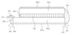
도 1 및 도 3에 도시된 바와 같이, 표시패널(DP)은 액정층(555)을 사이에 두고 서로 마주보는 하부 기판(361a)과 상부 기판(361b)을 포함한다.1 and 3, the display panel DP includes a
상부 기판(361a) 및 하부 기판(361b)은 각각 복수의 면들을 갖는다. 설명의 편의를 위해 이 복수의 면들은 다음과 같은 용어로 정의된다. 즉, 액정층(555)을 사이에 두고 마주보는 면들 각각은 해당 기판의 앞면으로 정의되고, 앞면을 기준으로 그 반대편에 위치한 면은 해당 기판의 뒷면으로 정의되고, 그리고 해당 기판에 포함된 앞면의 모서리들과 뒷면의 모서리들 사이에 위치한 면들은 측면들로 정의된다.Each of the
하부 기판(361a)은, 도 1에 도시된 바와 같이, 표시 영역(A1)과 비표시 영역(A2)으로 구분된다. 하부 기판(361a)의 앞면 중 표시 영역(A1)에 해당하는 부분 위에, 도 2에 도시된 바와 같이, 복수의 게이트 라인들(GL1 내지 GLi)과, 이 게이트 라인들(GL1 내지 GLi)과 교차되는 복수의 데이터 라인들(DL1 내지 DLj)과, 그리고 게이트 라인들(GL1 내지 GLi)과 데이터 라인들(GL1 내지 GLi)에 접속된 박막 트랜지스터(TFT)들이 배치된다.The
도 3에 도시된 바와 같이, 상부 기판(361b)은 하부 기판(361a) 위에 위치한다. 상부 기판(361b)은 적어도 하부 기판(361a)의 표시 영역(A1)의 전체면을 가릴 수 있을 정도의 크기를 갖는다. 3, the
도시되지 않았지만, 상부 기판의 앞면 위에 블랙 매트릭스, 복수의 컬러필터들 및 공통 전극이 위치한다. Although not shown, a black matrix, a plurality of color filters, and a common electrode are positioned on the front surface of the upper substrate.
블랙 매트릭스는, 상기 앞면 중 화소 영역들에 대응되는 부분들을 제외한 나머지 부분 위에 위치한다.The black matrix is positioned on the rest of the front surface except for portions corresponding to pixel areas.
컬러필터들은 화소 영역에 위치한다. 컬러필터들은 적색 컬러필터, 녹색 컬러필터 및 청색 컬러필터로 구분된다.The color filters are located in the pixel area. The color filters are divided into a red color filter, a green color filter, and a blue color filter.
상부 기판(361b)의 앞면 중 이의 가장자리를 따라 시일재(sealant)가 위치한다. 이 시일재에 의해 상부 기판(361b)과 하부 기판(361a)이 서로 접합됨과 아울러, 상부 기판과 하부 기판(361a) 사이의 공간을 밀봉한다.A sealant is positioned along the edge of the front surface of the
화소들(R, B, B)은 표시 영역(A1)에 행렬 형태로 배열된다. 화소들(R, G, B)은 적색 컬러필터에 대응하여 위치한 적색 화소(R)들, 녹색 컬러필터에 대응하여 위치한 녹색 화소(G) 및 청색 컬러필터에 대응하여 위치한 청색 화소(B)로 구분된다. 이때, 수평 방향으로 인접한 적색 화소(R), 녹색 화소(G) 및 청색 화소(B)는 하나의 단위 영상을 표시하기 위한 단위 화소가 될 수 있다.The pixels R, B, and B are arranged in a matrix form in the display area A1. The pixels R, G, and B include red pixels R located corresponding to the red color filter, green pixels G located corresponding to the green color filter, and blue pixels B located corresponding to the blue color filter. It is distinguished. In this case, the red pixels R, the green pixels G, and the blue pixels B adjacent in the horizontal direction may be unit pixels for displaying one unit image.
제 n 수평라인(n은 1 내지 i 중 어느 하나)을 따라 배열된 j개의 화소들(이하, 제 n 수평라인 화소들)은 제 1 내지 제 j 데이터 라인들(DL1 내지 DLj) 각각에 개별적으로 접속된다. 아울러, 이 제 n 수평라인 화소들은 제 n 게이트 라인에 공통으로 접속된다. 이에 따라, 제 n 수평라인 화소들은 제 n 게이트 신호를 공통으로 공급받는다. 즉, 동일 수평라인 상에 배열된 j개의 화소들은 모두 동일한 게이트 신호를 공급받지만, 서로 다른 수평라인 상에 위치한 화소들은 서로 다른 게이트 신호를 공급받는다. 예를 들어, 제 1 수평라인(HL1)에 위치한 적색 화소(R) 및 녹색 화소(G)는 모두 제 1 게이트 신호를 공급받는 반면, 제 2 수평라인(HL2)에 위치한 적색 화소(R) 및 녹색 화소(G)는 이들과는 다른 타이밍을 갖는 제 2 게이트 신호를 공급받는다.The j pixels (hereinafter, n-th horizontal line pixels) arranged along the n-th horizontal line (n is any one of 1 to i) are individually provided to each of the first to j-th data lines DL1 to DLj. Connected. In addition, the nth horizontal line pixels are commonly connected to the nth gate line. Accordingly, the n-th horizontal line pixels receive the n-th gate signal in common. That is, all j pixels arranged on the same horizontal line receive the same gate signal, but pixels located on different horizontal lines receive different gate signals. For example, the red pixel R and the green pixel G located on the first horizontal line HL1 both receive the first gate signal, while the red pixel R and the green pixel R located on the second horizontal line HL2 The green pixel G receives a second gate signal having a timing different from these.
각 화소는, 도 4에 도시된 바와 같이, 박막 트랜지스터(TFT), 액정용량 커패시터(CLC) 및 보조용량 커패시터(Cst)를 포함한다.Each pixel, as shown in FIG. 4, includes a thin film transistor TFT, a liquid crystal capacitor CLC , and an auxiliary capacitor Cst.
박막 트랜지스터(TFT)는 게이트 라인으로부터의 게이트 신호에 따라 턴-온된다. 턴-온된 박막 트랜지스터(TFT)는 데이터 라인으로부터 제공된 아날로그 영상 데이터 신호를 액정용량 커패시터(CLC) 및 보조용량 커패시터(Cst)로 공급한다.The thin film transistor TFT is turned on according to a gate signal from a gate line. The turned-on thin film transistor TFT supplies the analog image data signal provided from the data line to the liquid crystal capacitor CLC and the auxiliary capacitor Cst.
액정용량 커패시터(CLC)는 서로 대향하여 위치한 화소 전극과 공통 전극을 포함한다.The liquid crystal capacitor CLC includes a pixel electrode and a common electrode positioned opposite to each other.
보조용량 커패시터(Cst)는 서로 대향하여 위치한 화소 전극과 대향 전극을 포함한다. 여기서, 대향 전극은 전단 게이트 라인 또는 공통 전압을 전송하는 공통 라인이 될 수 있다.The storage capacitor capacitor Cst includes a pixel electrode and an opposite electrode positioned to face each other. Here, the opposite electrode may be a front gate line or a common line for transmitting a common voltage.
데이터 구동 집적회로(222)들은, 도 1에 도시된 바와 같이, 데이터 캐리어 테입(carrier tape; 211)들에 하나씩 실장(mount)된다.The data driving
데이터 캐리어 테입(211)은 필름(flim) 형태로 제조될 수 있다.The
데이터 구동 집적회로(222)가 실장된 캐리어 테입은 데이터 테입 캐리어 패키지(Tape Carrier Package)로도 불린다.The carrier tape on which the data driving
데이터 캐리어 테입(211)들은 인쇄회로기판(401)과 표시패널(DP)을 전기적으로 연결한다. 이를 위해, 예를 들어, 캐리어 테입들의 입력 단자들은 인쇄회로기판(401)에 형성된 신호배선패턴들(도시되지 않음)에 접속되고, 데이터 캐리어 테입(211)들의 출력 단자들은 표시패널(DP)의 비표시 영역(A2)에 형성된 데이터 패드부(도시되지 않음)에 접속된다.The
데이터 패드부는 데이터 링크 라인들을 통해 데이터 라인들(DL1 내지 DLj)에 연결된다.The data pad unit is connected to the data lines DL1 to DLj through data link lines.
입력 단자들이 위치한 데이터 캐리어 테입(211)의 일측과 인쇄회로기판(401)은 이방성 도전성 필름(Anisotropic conductive bonding Film)에 의해 접착될 수 있다. 또한, 출력 단자들이 위치한 데이터 캐리어 테입(211)의 타측과 표시패널(DP)은 이방성 도전성 필름에 의해 접착될 수 있다.One side of the
데이터 캐리어 테입(211)들은 구부러질 수 있는 연성 재질로 이루어질 수 있다. 예를 들어, 데이터 캐리어 테입(211)들은 열팽창 계수(CTE : coefficient of thermal expansion)나 내구성이 우수한 재질인 폴리이미드(polyimide)로 제조될 수 있다. 그 외에도, 아크릴(acrylic), 폴리에테르니트릴(polyether nitrile), 폴리에테르술폰(polyethersulfone), 폴리에틸렌 테레프탈레이트(polyethylene terephthalate), 폴리에틸렌 나프탈레이드(polyethylenenaphthalate) 등의 합성수지가 사용될 수도 있다.The
데이터 패드부는 비표시 영역(A2) 중 표시 영역(A1)의 상측 가장자리에 인접한 부분에 위치할 수 있다.The data pad part may be located in a portion of the non-display area A2 adjacent to the upper edge of the display area A1.
데이터 캐리어 테입(211)들의 출력 단자들은 비표시 영역(A2) 중 표시 영역(A1)의 상측 가장자리에 인접한 부분에 위치할 수 있다.Output terminals of the
신호배선패턴들 중 일부는 타이밍 컨트롤러로부터 제공된 디지털 영상 데이터 신호들 및 데이터 제어신호를 데이터 구동 집적회로(222)들로 전송한다. 이때, 데이터 구동 집적회로(222)는 데이터 캐리어 테입(211)에 형성된 입력배선패턴들(도시되지 않음)을 통해 디지털 영상 데이터 신호들 및 데이터 제어신호를 제공받는다. 그리고, 데이터 구동 집적회로(222)는 데이터 캐리어 테입(211)에 형성된 출력배선패턴들을 통해 아날로그 영상 데이터 신호들을 출력한다. 여기서, 각 입력배선패턴의 끝단이 전술된 입력 단자에 해당하며, 각 출력배선패턴의 끝단이 전술된 출력 단자에 해당된다.Some of the signal wiring patterns transmit digital image data signals and data control signals provided from the timing controller to the data driving
신호배선패턴들 중 다른 일부는, 어느 하나의 데이터 캐리어 테입(211)에 형성된 보조 배선패턴들(도시되지 않음) 및 하부 기판(361a)의 모서리에 형성된 제 1 보조 라인들(도시되지 않음)을 통해, 게이트 구동 집적회로(333)들로 게이트 제어신호를 전송한다. 보조 배선패턴들은 전체 데이터 캐리어 테입(211)들 중 최외각에 위치한 하나의 데이터 캐리어 테입(211)에 형성될 수 있다. 예를 들어, 도 1에 도시된 바와 같이, 가장 좌측에 위치한 하나의 데이터 캐리어 테입(601)에 보조 배선패턴들이 형성될 수 있다.Some of the signal wiring patterns include auxiliary wiring patterns (not shown) formed on any one
타이밍 컨트롤러 및 전원 공급부는 인쇄회로기판(402)에 위치할 수 있다.The timing controller and the power supply may be located on the printed circuit board 402.
게이트 구동 집적회로(333)들은, 도 1에 도시된 바와 같이, 게이트 캐리어 테입(gate carrier tape; 311)들에 하나씩 실장(mount)된다.The gate driving
게이트 캐리어 테입(311)은 필름 형태로 제조될 수 있다.The
게이트 구동 집적회로(333)가 실장된 게이트 캐리어 테입(311)은 게이트 테입 캐리어 패키지(Tape Carrier Package)로도 불린다.The
게이트 구동 집적회로(333)들은 게이트 제어신호에 따라 게이트 신호들을 발생시킨다. 게이트 구동 집적회로(333)들로부터 출력된 게이트 신호들은 게이트 라인들(GL1 내지 GLi)에 순차적으로 공급된다.The gate driving
게이트 캐리어 테입(311)들의 입력 단자들은 제 2 보조 라인들(도시되지 않음)에 연결된다. 제 2 보조 라인들은 하부 기판(361a)의 비표시 영역에 형성된다. 이때, 제 2 보조 라인들은 서로 인접한 게이트 캐리어 테입(311)들 사이에 위치한다.Input terminals of the
보조 배선패턴들 및 제 1 보조 라인들을 통해 타이밍 컨트롤러로부터 제공된 게이트 제어신호는, 제 2 보조 라인들을 통해 각 게이트 캐리어 테입(311)들로 공급된다. 게이트 구동 집적회로(333)는 게이트 캐리어 테입(311)에 형성된 입력 단자를 통해 위의 게이트 제어신호를 공급받는다.The gate control signal provided from the timing controller through the auxiliary wiring patterns and the first auxiliary lines is supplied to the respective
게이트 캐리어 테입(311)들의 출력 단자들은 표시패널(DP)의 비표시 영역(A2)에 형성된 게이트 패드부(도시되지 않음)에 접속된다.Output terminals of the
게이트 패드부는 게이트 링크 라인들을 통해 게이트 라인들(GL1 내지 GLi)에 연결된다.The gate pad portion is connected to the gate lines GL1 to GLi through gate link lines.
출력 단자들이 위치한 게이트 캐리어 테입(311)의 일측과 표시패널(DP)은 이방성 도전성 필름에 의해 접착될 수 있다.One side of the
게이트 캐리어 테입(311)들은 구부러질 수 있는 연성 재질로 이루어질 수 있다. 예를 들어, 게이트 캐리어 테입(311)들은 열팽창 계수(CTE: coefficient of thermal expansion)나 내구성이 우수한 재질인 폴리이미드(polyimide)로 제조될 수 있다. 그 외에도, 아크릴(acrylic), 폴리에테르니트릴(polyether nitrile), 폴리에테르술폰(polyethersulfone), 폴리에틸렌 테레프탈레이트(polyethylene terephthalate), 폴리에틸렌 나프탈레이드(polyethylenenaphthalate) 등의 합성수지가 사용될 수도 있다.The
게이트 패드부들은 비표시 영역(A2) 중 표시 영역(A1)의 좌측 가장자리에 인접한 부분에 위치할 수 있다.The gate pad portions may be located in a portion of the non-display area A2 adjacent to the left edge of the display area A1.
게이트 캐리어 테입(311)들의 타측 단자들은 비표시 영역(A2) 중 표시 영역(A1)의 좌측 가장자리에 인접한 부분에 위치할 수 있다.Other terminals of the
한편, 도 3에 도시된 바와 같이, 하부 기판(361a)의 뒷면 위에 하부 편광판(501a)이 위치하고, 상부 기판(361b)의 뒷면 위에 상부 편광판(501b)이 위치한다.Meanwhile, as shown in FIG. 3, a lower
상부 편광판(501b) 및 하부 편광판(501a)은 각각 복수의 면들을 갖는다. 설명의 편의를 위해 이 복수의 면들은 다음과 같은 용어로 정의된다. 즉, 액정층(555) 및 양 기판들을 사이에 두고 마주보는 면들 각각은 해당 편광판의 앞면으로 정의되고, 앞면을 기준으로 그 반대편에 위치한 면은 해당 편광판의 뒷면으로 정의되고, 그리고 해당 편광판에 포함된 앞면의 모서리들과 뒷면의 모서리들 사이에 위치한 면들은 측면들로 정의된다.Each of the upper
도 3에 따르면, 상부 편광판(501b)은 상부 기판(361b)보다 작은 면적을 갖는다.Referring to FIG. 3, the upper
도 3에 따르면, 하부 편광판(501a)의 일측(881)이, 하부 기판(361a)(또는 상부 기판(361b))의 측면에서 연장된 가상의 연장면(801)을 교차한다. 이에 따라, 하부 편광판(501a)의 일측(881)이 하부 기판(361a)의 뒷면과 접촉하지 않는다. 그리고, 이 하부 편광판(501a)의 일측(881)이 하부 기판(361a)의 측면보다 더 외곽으로 돌출된다. 이하, 설명의 편의상 이 하부 편광판(501a)의 일측(881)을 제 1 하부 돌출부(881)로 고쳐 부른다.Referring to FIG. 3, one
또한, 도 3에 따르면, 하부 편광판(501a)의 타측(882)이, 하부 기판(361a)의 측면에서 연장된 가상의 연장면(802)을 교차한다. 이에 따라, 하부 편광판(501a)의 타측(882)이 하부 기판(361a)의 뒷면과 접촉하지 않으며, 그리고 이 하부 편광판(501a)의 타측(882)이 하부 기판(361a)의 측면보다 더 외곽으로 돌출된다. 이하, 설명의 편의상 이 하부 편광판(501a)의 타측(882)을 제 2 하부 돌출부(882)로 고쳐 부른다.In addition, according to FIG. 3, the
하부 편광판(501a)은 하부 기판(361a)의 면적보다 클 수도 있고 작을 수도 있다. 물론, 하부 편광판(501a)의 면적과 하부 기판(361a)의 면적이 같을 수도 있다.The lower
차광 시일재(685)는 양 기판(361a, 361b)에 포함된 복수의 측면들 중 적어도 하나의 위에 위치한다. 예를 들어, 차광 시일재(685)는, 도 3에 도시된 바와 같이, 하부 기판(361a)의 제 1 측면(도 3의 우측에 위치한 측면) 위와, 하부 기판(361a)의 제 2 측면(도 3의 좌측에 위치한 측면) 위 및 상부 기판(361b)의 제 1 측면(도 3의 우측에 위치한 측면) 위에 도포된다.The
차광 시일재(685)를 도포하는 공정은, 상부 편광판(501b) 및 하부 편광판(501a)이 표시패널에 부착된 이후에 수행될 수 있다. 한편, 이는 하나의 예시일 뿐, 차광 시일재(685)를 도포하는 공정은 위와 같은 때가 아닌 다른 때에 수행될 수도 있다.The process of applying the light
차광 시일재(685)는 상부 기판(361b)의 모든 측면들과 하부 기판(361a)의 모든 측면들에 형성될 수 있다.The
하부 기판(361a)의 제 1 측면 및 상부 기판(361b)의 제 1 측면에 도포된 차광 시일재(685)의 일부는 제 1 하부 돌출부(881)의 앞면 및 측면 위에도 도포된다. 이때, 제 1 하부 돌출부(881)로 인해, 그 하부 기판(361a)의 제 1 측면 및 상부 기판(361b)의 제 1 측면에 도포된 차광 시일재(685)의 두께가 거의 균일해진다. 즉, 차광 시일재(685)의 중심부의 두께와 하측의 두께 간의 차이가 작아진다. 다시 말하여, 차광 시일재(685)의 하측 가장자리가 제 1 하부 돌출부(881)에 의해 들어 올려짐으로써 그 가장자리의 두께가 두꺼워질 수 있다. 따라서, 그 가장자리에서의 빛샘 현상이 최소화될 수 있다.A portion of the light
하부 기판(361a)의 제 2 측면에 도포된 차광 시일재(685)의 일부는 제 2 하부 돌출부(882)의 앞면 및 측면 위에도 도포된다. 이때, 제 2 하부 돌출부(882)로 인해, 그 하부 기판(361a)의 제 2 측면에 도포된 차광 시일재(685)의 두께가 거의 균일해진다. 즉, 차광 시일재(685)의 중심부의 두께와 하측의 두께 간의 차이가 작아진다. 다시 말하여, 차광 시일재(685)의 하측 가장자리가 제 2 하부 돌출부(882)에 의해 들어 올려짐으로써 그 가장자리의 두께가 두꺼워질 수 있다. 따라서, 그 가장자리에서의 빛샘 현상이 최소화될 수 있다.A part of the light
도 4는 도 1의 I-I`의 선을 따라 자른 단면도에 대한 다른 실시예를 나타낸 도면이다.FIG. 4 is a diagram illustrating another embodiment of a cross-sectional view taken along line I-I′ of FIG. 1.
도 4에 따르면, 상부 편광판(501b)의 일측(991)이, 상부 기판(361b)의 측면으에서 연장된 가상의 연장면(901)을 교차한다. 이에 따라, 상부 편광판(501b)의 일측(991)이 상부 기판(361b)의 뒷면과 접촉하지 않으며, 그리고 이 상부 편광판(501b)의 일측(991)이 하부 기판(361a)의 측면보다 더 외곽으로 돌출된다. 이하, 설명의 편의상 이 상부 편광판(501b)의 일측(991)을 제 1 상부 돌출부(991)로 고쳐 부른다.According to FIG. 4, one
상부 편광판(501b)은 상부 기판(361b)의 면적보다 클 수도 있고 작을 수도 있다. 물론, 상부 편광판(501b)의 면적과 상부 기판(361b)의 면적이 같을 수도 있다.The upper
도 4에 따르면, 하부 편광판(501a)은 전술된 제 2 하부 돌출부(882)를 포함한다.Referring to FIG. 4, the lower
하부 편광판(501a)은 하부 기판(361a)의 면적보다 클 수도 있고 작을 수도 있다. 물론, 하부 편광판(501a)의 면적과 하부 기판(361a)의 면적이 같을 수도 있다.The lower
차광 시일재(685)는 양 기판(361a, 361b)에 포함된 복수의 측면들 중 적어도 하나의 위에 위치한다. 예를 들어, 차광 시일재(685)는, 도 4에 도시된 바와 같이, 하부 기판(361a)의 제 1 측면(도 4의 우측에 위치한 측면) 위와, 하부 기판(361a)의 제 2 측면(도 4의 좌측에 위치한 측면) 위 및 상부 기판(361b)의 제 1 측면(도 4의 우측에 위치한 측면) 위에 도포된다.The
차광 시일재(685)를 도포하는 공정은, 예를 들어, 상부 편광판(501b) 및 하부 편광판(501a)이 표시패널에 부착된 이후에 수행될 수 있다 한편, 이는 하나의 예시일 뿐, 차광 시일재(685)를 도포하는 공정은 위와 같은 때가 아닌 다른 때에 수행될 수도 있다.The process of applying the light-shielding
차광 시일재(685)는 상부 기판(361b)의 모든 측면들과 하부 기판(361a)의 모든 측면들에 형성될 수 있다.The
하부 기판(361a)의 제 1 측면 및 상부 기판(361b)의 제 1 측면에 도포된 차광 시일재(685)의 일부는 제 1 상부 돌출부(991)의 앞면 및 측면 위에도 도포된다. 이때, 제 1 상부 돌출부(991)로 인해, 그 하부 기판(361a)의 제 1 측면 및 상부 기판(361b)의 제 1 측면에 도포된 차광 시일재(685)의 두께가 거의 균일해진다. 즉, 차광 시일재(685)의 중심부의 두께와 상측의 두께 간의 차이가 작아진다. 다시 말하여, 차광 시일재(685)의 상측 가장자리가 제 1 상부 돌출부(991)에 의해 들어 올려짐으로써 그 가장자리의 두께가 두꺼워질 수 있다. 따라서, 그 가장자리에서의 빛샘 현상이 최소화될 수 있다.A portion of the light
하부 기판(361a)의 제 2 측면에 도포된 차광 시일재(685)의 일부는 제 2 하부 돌출부(882)의 앞면 및 측면 위에도 도포된다. 이때, 제 2 하부 돌출부(882)로 인해, 그 하부 기판(361a)의 제 2 측면에 도포된 차광 시일재(685)의 두께가 거의 균일해진다. 즉, 차광 시일재(685)의 중심부의 두께와 하측의 두께 간의 차이가 작아진다. 다시 말하여, 차광 시일재(685)의 하측 가장자리가 제 2 하부 돌출부(882)에 의해 들어 올려짐으로써 그 가장자리의 두께가 두꺼워질 수 있다. 따라서, 그 가장자리에서의 빛샘 현상이 최소화될 수 있다.A part of the light
도 5는 도 1의 I-I`의 선을 따라 자른 단면도에 대한 또 다른 실시예를 나타낸 도면이다.FIG. 5 is a view showing another embodiment of a cross-sectional view taken along line II′ of FIG. 1.
도 5에 따르면, 상부 편광판(501b)은 전술된 제 1 상부 돌출부(991)를 포함하고, 그리고 하부 편광판(501a)은 제 1 하부 돌출부(881) 및 제 2 하부 돌출부(882)를 포함한다.Referring to FIG. 5, the upper
상부 편광판(501b)은 상부 기판(361b)의 면적보다 클 수도 있고 작을 수도 있다. 물론, 상부 편광판(501b)의 면적과 상부 기판(361b)의 면적이 같을 수도 있다.The upper
하부 편광판(501a)은 하부 기판(361a)의 면적보다 클 수도 있고 작을 수도 있다. 물론, 하부 편광판(501a)의 면적과 하부 기판(361a)의 면적이 같을 수도 있다.The lower
차광 시일재(685)는 양 기판(361a, 361b)에 포함된 복수의 측면들 중 적어도 하나의 위에 위치한다. 예를 들어, 도 5에 도시된 바와 같이, 하부 기판(361a)의 제 1 측면(도 5의 우측에 위치한 측면) 위와, 하부 기판(361a)의 제 2 측면(도 5의 좌측에 위치한 측면) 위 및 상부 기판(361b)의 제 1 측면(도 5의 우측에 위치한 측면) 위에 도포된다.The
차광 시일재(685)를 도포하는 공정은, 상부 편광판(501b) 및 하부 편광판(501a)이 표시패널에 부착된 이후에 수행될 수 있다. 한편, 이는 하나의 예시일 뿐, 차광 시일재(685)를 도포하는 공정은 위와 같은 때가 아닌 다른 때에 수행될 수도 있다.The process of applying the light
차광 시일재(685)는 상부 기판(361b)의 모든 측면들과 하부 기판(361a)의 모든 측면들에 형성될 수 있다.The
하부 기판(361a)의 제 1 측면 및 상부 기판(361b)의 제 1 측면에 도포된 차광 시일재(685)의 일부는 제 1 하부 돌출부(881) 및 제 1 상부 돌출부(991)의 앞면 및 측면 위에도 도포된다. 이때, 제 1 하부 돌출부(881) 및 제 1 상부 돌출부(991)로 인해, 그 하부 기판(361a)의 제 1 측면 및 상부 기판(361b)의 제 1 측면에 도포된 차광 시일재(685)의 두께가 거의 균일해진다. 즉, 차광 시일재(685)의 중심부의 두께, 상측의 두께 및 하측의 두께 간의 차이가 작아진다. 다시 말하여, 차광 시일재(685)의 하측 가장자리가 제 1 하부 돌출부(881)에 의해 들어 올려지고, 이의 상측 가장자리가 제 1 상부 돌출부(991)에 의해 들어올려짐으로써 양 가장자리의 두께가 두꺼워질 수 있다. 따라서, 양 가장자리에서의 빛샘 현상이 최소화될 수 있다.Part of the light
하부 기판(361a)의 제 2 측면에 도포된 차광 시일재(685)의 일부는 제 2 하부 돌출부(882)의 앞면 및 측면 위에도 도포된다. 이때, 제 2 하부 돌출부(882)로 인해, 그 하부 기판(361a)의 제 2 측면에 도포된 차광 시일재(685)의 두께가 거의 균일해진다. 즉, 차광 시일재(685)의 중심부의 두께와 하측의 두께 간의 차이가 작아진다. 다시 말하여, 차광 시일재(685)의 하측 가장자리가 제 2 하부 돌출부(882)에 의해 들어 올려짐으로써 그 가장자리의 두께가 두꺼워질 수 있다. 따라서, 그 가장자리에서의 빛샘 현상이 최소화될 수 있다.A part of the light
제 1 상부 돌출부(991)의 끝단과 제 1 하부 돌출부(881)의 끝단은 동일 면상에 위치할 수 있다.An end of the first
도 6은 도 1의 II-II`의 선을 따라 자른 단면도이다.6 is a cross-sectional view taken along the line II-II′ of FIG. 1.
하부 편광판(501a)의 일측(883)이, 하부 기판(361a)(또는 상부 기판(361b))의 측면에서 연장된 가상의 연장면(803)을 교차한다. 이에 따라, 하부 편광판(501a)의 일측(883)이 하부 기판(361a)의 뒷면과 접촉하지 않는다. 그리고, 이 하부 편광판(501a)의 일측(883)이 하부 기판(361a)의 측면보다 더 외곽으로 돌출된다. 이하, 설명의 편의상 이 하부 편광판(501a)의 일측(883)을 제 3 하부 돌출부(883)로 고쳐 부른다.One
또한, 도 6에 따르면, 하부 편광판(501a)의 타측(884)이, 하부 기판(361a)의 측면에서 연장된 가상의 연장면(804)을 교차한다. 이에 따라, 하부 편광판(501a)의 타측(884)이 하부 기판(361a)의 뒷면과 접촉하지 않으며, 그리고 이 하부 편광판(501a)의 타측(884)이 하부 기판(361a)의 측면보다 더 외곽으로 돌출된다. 이하, 설명의 편의상 이 하부 편광판(501a)의 타측(884)을 제 4 하부 돌출부(884)로 고쳐 부른다.Further, according to FIG. 6, the
하부 편광판(501a)은 하부 기판(361a)의 면적보다 클 수도 있고 작을 수도 있다. 물론, 하부 편광판(501a)의 면적과 하부 기판(361a)의 면적이 같을 수도 있다.The lower
또한, 도 6에 따르면, 상부 편광판(501b)의 일측(993)이, 상부 기판(361b)의 측면에서 연장된 가상의 연장면(903)을 교차한다. 이에 따라, 상부 편광판(501b)의 일측(993)이 상부 기판(361b)의 뒷면과 접촉하지 않으며, 그리고 이 상부 편광판(501b)의 일측(993)이 하부 기판(361a)의 측면보다 더 외곽으로 돌출된다. 이하, 설명의 편의상 이 상부 편광판(501b)의 일측(993)을 제 2 상부 돌출부(993)로 고쳐 부른다.Further, according to FIG. 6, one
하부 편광판(501a)은 하부 기판(361a)의 면적보다 클 수도 있고 작을 수도 있다. 물론, 하부 편광판(501a)의 면적과 하부 기판(361a)의 면적이 같을 수도 있다.The lower
차광 시일재(685)는 양 기판(361a, 361b)에 포함된 복수의 측면들 중 적어도 하나의 위에 위치한다. 예를 들어, 차광 시일재(685)는, 도 6에 도시된 바와 같이, 하부 기판(361a)의 제 3 측면(도 6의 우측에 위치한 측면) 위와, 하부 기판(361a)의 제 4 측면(도 6의 좌측에 위치한 측면) 위 및 상부 기판(361b)의 제 3 측면(도 6의 우측에 위치한 측면) 위에 도포된다.The
차광 시일재(685)를 도포하는 공정은, 상부 편광판(501b) 및 하부 편광판(501a)이 표시패널(DP)에 부착된 이후에 수행될 수 있다. 한편, 이는 하나의 예시일 뿐, 차광 시일재(685)를 도포하는 공정은 위와 같은 때가 아닌 다른 때에 수행될 수도 있다.The process of applying the light
차광 시일재(685)는 상부 기판(361b)의 모든 측면들과 하부 기판(361a)의 모든 측면들에 형성될 수 있다.The
하부 기판(361a)의 제 3 측면 및 상부 기판(361b)의 제 3 측면에 도포된 차광 시일재(685)의 일부는 제 3 하부 돌출부(883) 및 제 2 상부 돌출부(993)의 앞면 및 측면 위에도 도포된다. 이때, 제 3 하부 돌출부(883) 및 제 2 상부 돌출부(993)로 인해, 그 하부 기판(361a)의 제 3 측면 및 상부 기판(361b)의 제 3 측면에 도포된 차광 시일재(685)의 두께가 거의 균일해진다. 즉, 차광 시일재(685)의 중심부의 두께, 상측의 두께 및 하측의 두께 간의 차이가 작아진다. 다시 말하여, 차광 시일재(685)의 하측 가장자리가 제 3 하부 돌출부(883)에 의해 들어 올려지고, 이의 상측 가장자리가 제 2 상부 돌출부(993)에 의해 들어올려짐으로써 양 가장자리의 두께가 두꺼워질 수 있다. 따라서, 양 가장자리에서의 빛샘 현상이 최소화될 수 있다.Part of the light-shielding
하부 기판(361a)의 제 4 측면에 도포된 차광 시일재(685)의 일부는 제 4 하부 돌출부(884)의 앞면 및 측면 위에도 도포된다. 이때, 제 4 하부 돌출부(884)로 인해, 그 하부 기판(361a)의 제 4 측면에 도포된 차광 시일재(685)의 두께가 거의 균일해진다. 즉, 차광 시일재(685)의 중심부의 두께와 하측의 두께 간의 차이가 작아진다. 다시 말하여, 차광 시일재(685)의 하측 가장자리가 제 4 하부 돌출부(884)에 의해 들어 올려짐으로써 그 가장자리의 두께가 두꺼워질 수 있다. 따라서, 그 가장자리에서의 빛샘 현상이 최소화될 수 있다.A part of the light
제 2 상부 돌출부(993)의 끝단과 제 3 하부 돌출부(883)의 끝단은 동일 면상에 위치할 수 있다.An end of the second
한편, 도시되지 않았지만, II-II'의 선을 따라 자른 단면은, 전술된 도 3 및 도 4 중 어느 하나의 구조를 가질 수도 있다.Meanwhile, although not shown, the cross-section cut along the line II-II' may have any one of the above-described FIGS. 3 and 4.
제 1 하부 돌출부(881), 제 2 하부 돌출부(882), 제 1 상부 돌출부(991), 제 2 상부 돌출부(993), 제 3 하부 돌출부(883) 및 제 4 하부 돌출부(884)의 길이는 서로 같을 수도 있고, 다를 수도 있다.The lengths of the first
제 1 하부 돌출부(881), 제 2 하부 돌출부(882), 제 1 상부 돌출부(991), 제 2 상부 돌출부(993), 제 3 하부 돌출부(883) 및 제 4 하부 돌출부(884)는, 차광 시일재(685)의 광 차폐율에 따라, 각각 1um 내지 500um의 높이를 가질 수 있다. 차광 시일재(685)의 광 차폐율은 그 차광 시일재로 사용되는 재질에 따라 달라질 수 있다.The first
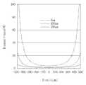
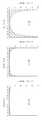
도 7 내지 9는 돌출부의 길이와 양 기판의 측면들로부터의 광 투과율 간의 상관관계를 설명하기 위한 도면이다. 도 9에서, 빗금친 영역은 광이 투과되는 영역, 즉 빛이 새는 영역을 나타낸 것이다.7 to 9 are diagrams for explaining a correlation between the length of the protrusion and the light transmittance from side surfaces of both substrates. In FIG. 9, the hatched area represents an area through which light is transmitted, that is, an area through which light leaks.
도 7에서 하부 기판(361a)과 상부 기판(361b) 사이에 위치한 구성요소들은 생략되었다.In FIG. 7, components located between the
도 7 내지 도 9에 도시된 바와 같이, 돌출부가 없는 종래의 경우, 측면의 중심부와 양 가장자리들 간의 광 투과율 차가 상당히 큼을 알 수 있다. 그러나, 돌출부의 길이가 100um 또는 200um 인 경우, 측면의 중심부와 양 가장자리들 간의 광 투과율 차가 상당히 작음을 알 수 있다.As shown in FIGS. 7 to 9, in the case of the conventional case without the protrusion, it can be seen that the difference in light transmittance between the center of the side and both edges is quite large. However, when the length of the protrusion is 100 μm or 200 μm, it can be seen that the difference in light transmittance between the center of the side and both edges is quite small.
게다가, 종래의 표시장치는, 도 7에 도시된 바와 같이, 약 20um 정도의 마진(margin) 영역을 반드시 필요로 한다. 이 마진 영역이 확보되어야만, 차광 시일재 도포 공정시 이 차광 시일재(685)가 기판의 뒷면으로 넘쳐 흐르는 것이 방지된다. 반면, 본 발명에 따른 표시장치는, 돌출부에 의해 차광 시일재(685)의 넘침이 방지될 수 있으므로, 종래와 같은 별도의 마진 영역을 필요로 하지 않는다.In addition, the conventional display device necessarily requires a margin area of about 20 μm, as shown in FIG. 7. Only when this margin area is secured, the light-shielding
이상에서 설명한 본 발명은 상술한 실시예 및 첨부된 도면에 한정되는 것이 아니고, 본 발명의 기술적 사상을 벗어나지 않는 범위 내에서 여러 가지 치환, 변형 및 변경이 가능하다는 것이 본 발명이 속하는 기술 분야에서 통상의 지식을 가진 자에게 있어 명백할 것이다.The present invention described above is not limited to the above-described embodiments and the accompanying drawings, and that various substitutions, modifications, and changes are possible within the scope of the technical spirit of the present invention. It will be obvious to those who have the knowledge of.
361a: 하부 기판361b: 상부 기판
501a: 하부 편광판501b: 상부 편광판
555: 액정층666: 시일재
801, 802, 901: 가상의 연장면881: 제 1 하부 돌출부
882: 제 2 하부 돌출부991: 제 1 상부 돌출부
311: 게이트 캐리어 테입333: 게이트 구동 집적회로
685: 차광 시일재361a:
501a: lower polarizing
555: liquid crystal layer 666: sealing material
801, 802, 901: virtual extension surface 881: first lower protrusion
882: second lower protrusion 991: first upper protrusion
311: gate carrier tape 333: gate driving integrated circuit
685: shading sealing material
Claims (8)
Translated fromKorean상기 제 1 기판과 대향하여 위치한 제 2 기판;
상기 제 1 기판 및 제 2 기판의 적어도 하나의 측면 상에 위치한 차광 시일재;
상기 제 1 기판 및 제 2 기판 중 어느 하나의 면상에 위치한 제 1 편광판; 및
상기 제 1 기판 및 제 2 기판 중 다른 하나의 면상에 위치한 제 2 편광판을 포함하며,
상기 제 1 편광판은 상기 적어도 하나의 측면에서 연장된 가상의 연장면과 교차하며,
상기 제 2 편광판은 상기 적어도 하나의 측면에서 연장된 가상의 연장면과 교차하는 표시장치.A first substrate having a display area and a non-display area;
A second substrate positioned opposite the first substrate;
A light blocking material positioned on at least one side surface of the first substrate and the second substrate;
A first polarizing plate positioned on one of the first and second substrates; And
And a second polarizing plate positioned on the other surface of the first substrate and the second substrate,
The first polarizing plate intersects a virtual extension surface extending from the at least one side surface,
The second polarizing plate crosses a virtual extension surface extending from the at least one side surface.
상기 차광 시일재는 상기 제 1 편광판의 측면 및 하면 중 적어도 하나와 접촉하는 표시장치.The method of claim 1,
The light blocking sealing material is in contact with at least one of a side surface and a lower surface of the first polarizing plate.
상기 제 1 편광판의 단부와 상기 측면 사이의 거리는 1um 내지 500um인 표시장치.The method of claim 1,
A display device in which a distance between an end portion of the first polarizing plate and the side surface is 1 um to 500 um.
상기 차광 시일재는 상기 제 2 편광판의 측면 및 하면 중 적어도 하나와 접촉하는 표시장치.The method of claim 1,
The light blocking sealing material is in contact with at least one of a side surface and a lower surface of the second polarizing plate.
상기 제 2 편광판의 단부와 상기 측면 사이의 거리는 1um 내지 500um인 표시장치.The method of claim 1,
A display device in which a distance between an end of the second polarizing plate and the side surface is 1 um to 500 um.
상기 제 1 편광판의 단부와 제 2 편광판의 단부가 동일 면상에 위치하는 표시장치.The method of claim 1,
A display device in which an end of the first polarizing plate and an end of the second polarizing plate are positioned on the same plane.
Priority Applications (2)
| Application Number | Priority Date | Filing Date | Title |
|---|---|---|---|
| KR1020140116991AKR102197826B1 (en) | 2014-09-03 | 2014-09-03 | Display device |
| US14/666,769US9880413B2 (en) | 2014-09-03 | 2015-03-24 | Display device |
Applications Claiming Priority (1)
| Application Number | Priority Date | Filing Date | Title |
|---|---|---|---|
| KR1020140116991AKR102197826B1 (en) | 2014-09-03 | 2014-09-03 | Display device |
Publications (2)
| Publication Number | Publication Date |
|---|---|
| KR20160028572A KR20160028572A (en) | 2016-03-14 |
| KR102197826B1true KR102197826B1 (en) | 2021-01-05 |
Family
ID=55402312
Family Applications (1)
| Application Number | Title | Priority Date | Filing Date |
|---|---|---|---|
| KR1020140116991AActiveKR102197826B1 (en) | 2014-09-03 | 2014-09-03 | Display device |
Country Status (2)
| Country | Link |
|---|---|
| US (1) | US9880413B2 (en) |
| KR (1) | KR102197826B1 (en) |
Families Citing this family (9)
| Publication number | Priority date | Publication date | Assignee | Title |
|---|---|---|---|---|
| KR20160056460A (en)* | 2014-11-11 | 2016-05-20 | 삼성디스플레이 주식회사 | Curved display device |
| CN204229083U (en)* | 2014-12-04 | 2015-03-25 | 京东方科技集团股份有限公司 | A kind of display panel and display device |
| KR102463913B1 (en)* | 2018-01-04 | 2022-11-07 | 삼성디스플레이 주식회사 | Display apparatus |
| CN108924300A (en)* | 2018-07-03 | 2018-11-30 | 京东方科技集团股份有限公司 | Backlight module and display device |
| CN109188785A (en)* | 2018-09-25 | 2019-01-11 | 南京中电熊猫平板显示科技有限公司 | A kind of liquid crystal module and its manufacturing method |
| CN110824750A (en)* | 2019-11-20 | 2020-02-21 | 京东方科技集团股份有限公司 | a display device |
| CN112859467A (en)* | 2020-07-08 | 2021-05-28 | 友达光电股份有限公司 | Display panel |
| CN113193136A (en)* | 2021-04-06 | 2021-07-30 | 深圳市华星光电半导体显示技术有限公司 | Display device and preparation method thereof |
| KR20240156512A (en)* | 2023-04-21 | 2024-10-30 | 동우 화인켐 주식회사 | Liquid crystal package and manufacturing method for the same, optical laminate including the same, and smart window including the same |
Family Cites Families (15)
| Publication number | Priority date | Publication date | Assignee | Title |
|---|---|---|---|---|
| US4695490A (en)* | 1985-10-15 | 1987-09-22 | Rca Corporation | Seal for liquid crystal display |
| JP3158667B2 (en)* | 1991-08-01 | 2001-04-23 | セイコーエプソン株式会社 | Method of manufacturing liquid crystal display element and method of reproducing liquid crystal display element |
| JP4649706B2 (en)* | 2000-06-08 | 2011-03-16 | ソニー株式会社 | Display device and portable terminal using the same |
| KR100487436B1 (en) | 2002-12-24 | 2005-05-03 | 엘지.필립스 엘시디 주식회사 | Touch Panel with Liquid Crystal Display Device |
| KR101174149B1 (en) | 2004-06-18 | 2012-08-14 | 엘지디스플레이 주식회사 | Module for liquid crystal display device and method of manufacturing thereof |
| EP1873577A1 (en)* | 2005-03-29 | 2008-01-02 | Mitsubishi Chemical Corporation | In-Cell TYPE POLARIZER COMPOSITION, In-Cell TYPE POLARIZER, In-Cell TYPE LAYERED LIGHT POLARIZER, AND LIQUID CRYSTAL ELEMENT USING THE SAME |
| KR20070017821A (en)* | 2005-08-08 | 2007-02-13 | 삼성전자주식회사 | LCD and its assembly method |
| JP5057321B2 (en)* | 2006-03-14 | 2012-10-24 | 株式会社ジャパンディスプレイウェスト | Manufacturing method of display device |
| GB2442056B (en)* | 2006-09-19 | 2011-04-27 | Smiths Group Plc | Displays |
| KR101108157B1 (en) | 2009-11-19 | 2012-01-31 | 삼성모바일디스플레이주식회사 | Organic light emitting display device |
| KR101436806B1 (en)* | 2012-03-08 | 2014-09-03 | 엘지디스플레이 주식회사 | Display apparatus and method for manufacturing the same |
| KR101347566B1 (en) | 2012-05-01 | 2014-01-06 | 엘지디스플레이 주식회사 | Display apparatus and method for manufacturing the same |
| KR20140005404A (en) | 2012-07-03 | 2014-01-15 | 인텔렉추얼디스커버리 주식회사 | Flexible display device |
| KR102076503B1 (en)* | 2013-01-24 | 2020-02-13 | 엘지디스플레이 주식회사 | Display panel and display device including the same |
| KR102120640B1 (en)* | 2013-11-06 | 2020-06-10 | 엘지디스플레이 주식회사 | Liquid Crystal Display Device and Method of manufacturing the same |
- 2014
- 2014-09-03KRKR1020140116991Apatent/KR102197826B1/enactiveActive
- 2015
- 2015-03-24USUS14/666,769patent/US9880413B2/ennot_activeExpired - Fee Related
Also Published As
| Publication number | Publication date |
|---|---|
| US9880413B2 (en) | 2018-01-30 |
| KR20160028572A (en) | 2016-03-14 |
| US20160062182A1 (en) | 2016-03-03 |
Similar Documents
| Publication | Publication Date | Title |
|---|---|---|
| KR102197826B1 (en) | Display device | |
| KR101307260B1 (en) | Line on glass type liquid crystal display device and method of fabricating the same | |
| KR102695728B1 (en) | Display device | |
| US8314899B2 (en) | Array substrate and display device | |
| CN111048569B (en) | Display panel and display device | |
| US8547505B2 (en) | Liquid crystal display | |
| US10001676B2 (en) | Display device | |
| CN106990590B (en) | Liquid crystal display device having a plurality of pixel electrodes | |
| TW201814464A (en) | Display device | |
| KR102178198B1 (en) | Liquid crystal display device | |
| US20160004110A1 (en) | Display panel and method of producing display panel | |
| JP2018124481A (en) | Display device | |
| US20110222015A1 (en) | Liquid crystal display | |
| US10816857B2 (en) | Display device | |
| US20190219862A1 (en) | Display device and manufacturing method thereof | |
| US20190025629A1 (en) | Display device and smart mobile device | |
| JP7166193B2 (en) | liquid crystal display | |
| US20120320301A1 (en) | Integrated circuit chip on film and liquid crystal display including the same | |
| US7619709B2 (en) | Liquid crystal display panel and fabricating method thereof | |
| US8773630B2 (en) | Display device | |
| KR101923479B1 (en) | Liquid Crystal Display Device | |
| JP2016139073A (en) | Liquid crystal display | |
| US11101297B2 (en) | Display device | |
| JP2019105665A (en) | Display device | |
| KR102150422B1 (en) | Liquid crystal display device |
Legal Events
| Date | Code | Title | Description |
|---|---|---|---|
| PA0109 | Patent application | Patent event code:PA01091R01D Comment text:Patent Application Patent event date:20140903 | |
| PG1501 | Laying open of application | ||
| A201 | Request for examination | ||
| PA0201 | Request for examination | Patent event code:PA02012R01D Patent event date:20190729 Comment text:Request for Examination of Application Patent event code:PA02011R01I Patent event date:20140903 Comment text:Patent Application | |
| E902 | Notification of reason for refusal | ||
| PE0902 | Notice of grounds for rejection | Comment text:Notification of reason for refusal Patent event date:20200512 Patent event code:PE09021S01D | |
| AMND | Amendment | ||
| E601 | Decision to refuse application | ||
| PE0601 | Decision on rejection of patent | Patent event date:20200909 Comment text:Decision to Refuse Application Patent event code:PE06012S01D Patent event date:20200512 Comment text:Notification of reason for refusal Patent event code:PE06011S01I | |
| X091 | Application refused [patent] | ||
| AMND | Amendment | ||
| PX0901 | Re-examination | Patent event code:PX09011S01I Patent event date:20200909 Comment text:Decision to Refuse Application Patent event code:PX09012R01I Patent event date:20200707 Comment text:Amendment to Specification, etc. | |
| PX0701 | Decision of registration after re-examination | Patent event date:20201014 Comment text:Decision to Grant Registration Patent event code:PX07013S01D Patent event date:20201012 Comment text:Amendment to Specification, etc. Patent event code:PX07012R01I Patent event date:20200909 Comment text:Decision to Refuse Application Patent event code:PX07011S01I Patent event date:20200707 Comment text:Amendment to Specification, etc. Patent event code:PX07012R01I | |
| X701 | Decision to grant (after re-examination) | ||
| GRNT | Written decision to grant | ||
| PR0701 | Registration of establishment | Comment text:Registration of Establishment Patent event date:20201228 Patent event code:PR07011E01D | |
| PR1002 | Payment of registration fee | Payment date:20201229 End annual number:3 Start annual number:1 | |
| PG1601 | Publication of registration | ||
| PR1001 | Payment of annual fee | Payment date:20241125 Start annual number:5 End annual number:5 |