KR102193700B1 - Display device using semiconductor light emitting device - Google Patents
Display device using semiconductor light emitting deviceDownload PDFInfo
- Publication number
- KR102193700B1 KR102193700B1KR1020180080713AKR20180080713AKR102193700B1KR 102193700 B1KR102193700 B1KR 102193700B1KR 1020180080713 AKR1020180080713 AKR 1020180080713AKR 20180080713 AKR20180080713 AKR 20180080713AKR 102193700 B1KR102193700 B1KR 102193700B1
- Authority
- KR
- South Korea
- Prior art keywords
- light emitting
- semiconductor light
- emitting device
- insulating layer
- electrode
- Prior art date
- Legal status (The legal status is an assumption and is not a legal conclusion. Google has not performed a legal analysis and makes no representation as to the accuracy of the status listed.)
- Active
Links
Images


Classifications
- H01L27/156—
- H—ELECTRICITY
- H10—SEMICONDUCTOR DEVICES; ELECTRIC SOLID-STATE DEVICES NOT OTHERWISE PROVIDED FOR
- H10H—INORGANIC LIGHT-EMITTING SEMICONDUCTOR DEVICES HAVING POTENTIAL BARRIERS
- H10H29/00—Integrated devices, or assemblies of multiple devices, comprising at least one light-emitting semiconductor element covered by group H10H20/00
- H10H29/10—Integrated devices comprising at least one light-emitting semiconductor component covered by group H10H20/00
- H10H29/14—Integrated devices comprising at least one light-emitting semiconductor component covered by group H10H20/00 comprising multiple light-emitting semiconductor components
- H10H29/142—Two-dimensional arrangements, e.g. asymmetric LED layout
- H—ELECTRICITY
- H01—ELECTRIC ELEMENTS
- H01L—SEMICONDUCTOR DEVICES NOT COVERED BY CLASS H10
- H01L25/00—Assemblies consisting of a plurality of semiconductor or other solid state devices
- H01L25/03—Assemblies consisting of a plurality of semiconductor or other solid state devices all the devices being of a type provided for in a single subclass of subclasses H10B, H10D, H10F, H10H, H10K or H10N, e.g. assemblies of rectifier diodes
- H01L25/04—Assemblies consisting of a plurality of semiconductor or other solid state devices all the devices being of a type provided for in a single subclass of subclasses H10B, H10D, H10F, H10H, H10K or H10N, e.g. assemblies of rectifier diodes the devices not having separate containers
- H01L25/075—Assemblies consisting of a plurality of semiconductor or other solid state devices all the devices being of a type provided for in a single subclass of subclasses H10B, H10D, H10F, H10H, H10K or H10N, e.g. assemblies of rectifier diodes the devices not having separate containers the devices being of a type provided for in group H10H20/00
- H01L25/0753—Assemblies consisting of a plurality of semiconductor or other solid state devices all the devices being of a type provided for in a single subclass of subclasses H10B, H10D, H10F, H10H, H10K or H10N, e.g. assemblies of rectifier diodes the devices not having separate containers the devices being of a type provided for in group H10H20/00 the devices being arranged next to each other
- H01L33/005—
- H01L33/22—
- H01L33/40—
- H—ELECTRICITY
- H10—SEMICONDUCTOR DEVICES; ELECTRIC SOLID-STATE DEVICES NOT OTHERWISE PROVIDED FOR
- H10H—INORGANIC LIGHT-EMITTING SEMICONDUCTOR DEVICES HAVING POTENTIAL BARRIERS
- H10H20/00—Individual inorganic light-emitting semiconductor devices having potential barriers, e.g. light-emitting diodes [LED]
- H10H20/01—Manufacture or treatment
- H—ELECTRICITY
- H10—SEMICONDUCTOR DEVICES; ELECTRIC SOLID-STATE DEVICES NOT OTHERWISE PROVIDED FOR
- H10H—INORGANIC LIGHT-EMITTING SEMICONDUCTOR DEVICES HAVING POTENTIAL BARRIERS
- H10H20/00—Individual inorganic light-emitting semiconductor devices having potential barriers, e.g. light-emitting diodes [LED]
- H10H20/80—Constructional details
- H10H20/81—Bodies
- H10H20/819—Bodies characterised by their shape, e.g. curved or truncated substrates
- H10H20/82—Roughened surfaces, e.g. at the interface between epitaxial layers
- H—ELECTRICITY
- H10—SEMICONDUCTOR DEVICES; ELECTRIC SOLID-STATE DEVICES NOT OTHERWISE PROVIDED FOR
- H10H—INORGANIC LIGHT-EMITTING SEMICONDUCTOR DEVICES HAVING POTENTIAL BARRIERS
- H10H20/00—Individual inorganic light-emitting semiconductor devices having potential barriers, e.g. light-emitting diodes [LED]
- H10H20/80—Constructional details
- H10H20/83—Electrodes
- H10H20/832—Electrodes characterised by their material
- H—ELECTRICITY
- H10—SEMICONDUCTOR DEVICES; ELECTRIC SOLID-STATE DEVICES NOT OTHERWISE PROVIDED FOR
- H10H—INORGANIC LIGHT-EMITTING SEMICONDUCTOR DEVICES HAVING POTENTIAL BARRIERS
- H10H20/00—Individual inorganic light-emitting semiconductor devices having potential barriers, e.g. light-emitting diodes [LED]
- H10H20/80—Constructional details
- H10H20/84—Coatings, e.g. passivation layers or antireflective coatings
- H—ELECTRICITY
- H10—SEMICONDUCTOR DEVICES; ELECTRIC SOLID-STATE DEVICES NOT OTHERWISE PROVIDED FOR
- H10H—INORGANIC LIGHT-EMITTING SEMICONDUCTOR DEVICES HAVING POTENTIAL BARRIERS
- H10H20/00—Individual inorganic light-emitting semiconductor devices having potential barriers, e.g. light-emitting diodes [LED]
- H10H20/80—Constructional details
- H10H20/85—Packages
- H10H20/857—Interconnections, e.g. lead-frames, bond wires or solder balls
- H—ELECTRICITY
- H10—SEMICONDUCTOR DEVICES; ELECTRIC SOLID-STATE DEVICES NOT OTHERWISE PROVIDED FOR
- H10H—INORGANIC LIGHT-EMITTING SEMICONDUCTOR DEVICES HAVING POTENTIAL BARRIERS
- H10H29/00—Integrated devices, or assemblies of multiple devices, comprising at least one light-emitting semiconductor element covered by group H10H20/00
- H10H29/20—Assemblies of multiple devices comprising at least one light-emitting semiconductor device covered by group H10H20/00
- H10H29/24—Assemblies of multiple devices comprising at least one light-emitting semiconductor device covered by group H10H20/00 comprising multiple light-emitting semiconductor devices
- H—ELECTRICITY
- H10—SEMICONDUCTOR DEVICES; ELECTRIC SOLID-STATE DEVICES NOT OTHERWISE PROVIDED FOR
- H10H—INORGANIC LIGHT-EMITTING SEMICONDUCTOR DEVICES HAVING POTENTIAL BARRIERS
- H10H29/00—Integrated devices, or assemblies of multiple devices, comprising at least one light-emitting semiconductor element covered by group H10H20/00
- H10H29/80—Constructional details
- H10H29/85—Packages
- H10H29/857—Interconnections
- H—ELECTRICITY
- H10—SEMICONDUCTOR DEVICES; ELECTRIC SOLID-STATE DEVICES NOT OTHERWISE PROVIDED FOR
- H10H—INORGANIC LIGHT-EMITTING SEMICONDUCTOR DEVICES HAVING POTENTIAL BARRIERS
- H10H20/00—Individual inorganic light-emitting semiconductor devices having potential barriers, e.g. light-emitting diodes [LED]
- H10H20/01—Manufacture or treatment
- H10H20/034—Manufacture or treatment of coatings
- H—ELECTRICITY
- H10—SEMICONDUCTOR DEVICES; ELECTRIC SOLID-STATE DEVICES NOT OTHERWISE PROVIDED FOR
- H10H—INORGANIC LIGHT-EMITTING SEMICONDUCTOR DEVICES HAVING POTENTIAL BARRIERS
- H10H20/00—Individual inorganic light-emitting semiconductor devices having potential barriers, e.g. light-emitting diodes [LED]
- H10H20/01—Manufacture or treatment
- H10H20/036—Manufacture or treatment of packages
- H10H20/0364—Manufacture or treatment of packages of interconnections
Landscapes
- Engineering & Computer Science (AREA)
- Power Engineering (AREA)
- Microelectronics & Electronic Packaging (AREA)
- Physics & Mathematics (AREA)
- Condensed Matter Physics & Semiconductors (AREA)
- General Physics & Mathematics (AREA)
- Computer Hardware Design (AREA)
- Devices For Indicating Variable Information By Combining Individual Elements (AREA)
- Led Device Packages (AREA)
- Electroluminescent Light Sources (AREA)
Abstract
Translated fromKorean
Description
Translated fromKorean본 발명은 디스플레이 장치 및 이의 제조방법에 관한 것으로 특히, 반도체 발광소자를 이용한 플렉서블 디스플레이에 장치에 관한 것이다.The present invention relates to a display device and a method of manufacturing the same, and more particularly, to a device for a flexible display using a semiconductor light emitting device.
최근에는 디스플레이 기술분야에서 박형, 플렉서블 등의 우수한 특성을 가지는 디스플레이 장치가 개발되고 있다. 이에 반해, 현재 상용화된 주요 디스플레이는 LCD(Liguid Crystal Display)와 AMOLED(Active Matrix Organic Light Emitting Diodes)로 대표되고 있다.In recent years, in the field of display technology, a display device having excellent characteristics such as thin and flexible has been developed. In contrast, major displays currently commercially available are represented by LCD (Liguid Crystal Display) and AMOLED (Active Matrix Organic Light Emitting Diodes).
그러나, LCD의 경우에 빠르지 않은 반응 시간과, 플렉서블의 구현이 어렵다는 문제점이 존재하고, AMOLED의 경우에 수명이 짧고, 양산 수율이 좋지 않다는 취약점이 존재한다.However, in the case of LCD, there is a problem that the reaction time is not fast and it is difficult to implement the flexible, and in the case of AMOLED, there is a vulnerability that the lifespan is short and the mass production yield is not good.
한편, 발광 다이오드(Light Emitting Diode: LED)는 전류를 빛으로 변환시키는 잘 알려진 반도체 발광소자로서, 1962년 GaAsP 화합물 반도체를 이용한 적색 LED가 상품화된 것을 시작으로 GaP:N 계열의 녹색 LED와 함께 정보 통신기기를 비롯한 전자장치의 표시 화상용 광원으로 이용되어 왔다. 따라서, 상기 반도체 발광소자를 이용하여 디스플레이를 구현하여, 상기의 문제점을 해결하는 방안이 제시될 수 있다.On the other hand, Light Emitting Diode (LED) is a well-known semiconductor light emitting device that converts current into light. Starting with the commercialization of red LED using GaAsP compound semiconductor in 1962, information along with GaP:N series green LED It has been used as a light source for display images in electronic devices including communication devices. Accordingly, a method of solving the above problem by implementing a display using the semiconductor light emitting device may be proposed.
상기에서 설명된 본 발명의 반도체 발광소자를 이용한 디스플레이 장치에는 성장기판에서 반도체 발광소자를 분리하기 위해서는 레이저 리프트 오프법(Laser Lift-off, LLO) 또는 화학적 리프트 오프법(Chemical Lift-off, CLO)을 이용하여 분리할 수 있다.In the display device using the semiconductor light emitting device of the present invention described above, in order to separate the semiconductor light emitting device from the growth substrate, a laser lift-off method (LLO) or a chemical lift-off method (CLO). Can be separated by using.
나아가, 성장기판에서 반도체 발광소자를 분리하고 기판 상에 반도체 발광소자를 조립하는 방법으로 스탬프(stamp) 방식, 정전 척(chunk) 방식이 수행될 수 있다. 정전 척을 이용하여 반도체 발광소자를 조립하는 경우에 정전 척에 한번에 장착될 수 있는 반도체 발광소자의 개수가 제한되며, 정전 척의 유지 보수 비용이 높다는 문제점이 있다.Further, as a method of separating the semiconductor light emitting device from the growth substrate and assembling the semiconductor light emitting device on the substrate, a stamp method or an electrostatic chuck method may be performed. When assembling a semiconductor light emitting device using an electrostatic chuck, there is a problem that the number of semiconductor light emitting devices that can be mounted on the electrostatic chuck is limited, and the maintenance cost of the electrostatic chuck is high.
한편, 스탬프 방식은 앵커구조를 형성한 성장기판에 기판을 스탬핑하여 반도체 발광소자를 조립하는 방식으로, 조립을 원하지 않는 반도체 발광소자가 기판상에 전사되는 과전사 불량이 발생할 수도 있다. 스탬프 방식에서 반도체 발광소자의 과전사를 방지하기 위하여 온도, 압력과 같은 공정 조건 조절할 수 있다. 하지만, 과전사를 방지하기 위해서 온도 및 압력을 낮추는 과정에서 미전사 문제가 발생하게 되어 공정성이 떨어지게 된다는 문제점이 있다.Meanwhile, the stamp method is a method of assembling a semiconductor light emitting device by stamping a substrate on a growth substrate having an anchor structure, and an overtransfer failure may occur in which semiconductor light emitting devices that do not want to be assembled are transferred onto the substrate. In the stamp method, process conditions such as temperature and pressure can be adjusted to prevent overtransfer of the semiconductor light emitting device. However, there is a problem in that a non-transfer problem occurs in the process of lowering the temperature and pressure in order to prevent over-transfer, resulting in poor fairness.
이와 같이, 반도체 발광소자를 이용한 디스플레이의 경우에 반도체 발광소자를 조립하는 과정에서 과전사 불량이 발생하여 이를 개선할 필요가 있다. 이에 본 발명에서 디스플레이 장치의 조립 과정에서 과전사 불량이 개선된 디스플레이 장치 구조에 대하여 제시한다.As described above, in the case of a display using a semiconductor light emitting device, an overtransfer defect occurs in the process of assembling the semiconductor light emitting device, and this needs to be improved. Accordingly, in the present invention, a structure of a display device in which an overtransfer defect is improved during the assembly process of the display device is presented.
본 발명의 일 목적은 성장기판에서 반도체 발광소자를 조립하는 과정에서 과전사 불량이 방지된 디스플레이 장치 및 그 제조방법을 제공하기 위한 것이다.An object of the present invention is to provide a display device and a method of manufacturing the same in which overtransfer defects are prevented in the process of assembling a semiconductor light emitting device in a growth substrate.
또한 본 발명의 다른 일 목적은 공정 속도를 향상시킬 수 있는 디스플레이 장치 및 그 제조방법을 제공하기 위한 것이다.In addition, another object of the present invention is to provide a display device and a method of manufacturing the same that can improve the process speed.
본 발명에 따른 디스플레이 장치는 기판상에 복수의 반도체 발광소자들을 구비하고, 상기 기판은, 베이스 기판; 상기 베이스 기판 상에 구비된 절연층; 및 상기 절연층보다 돌출되도록 형성되고 상기 반도체 발광소자가 조립되도록 형성되는 패드를 포함하고, 상기 절연층은 무기입자를 포함하고, 상기 무기입자의 적어도 일부는 상기 절연층의 표면으로 돌출되도록 형성되는 것을 특징으로 하는 것을 특징으로 한다.A display device according to the present invention includes a plurality of semiconductor light emitting devices on a substrate, the substrate comprising: a base substrate; An insulating layer provided on the base substrate; And a pad formed to protrude from the insulating layer and formed to assemble the semiconductor light emitting device, wherein the insulating layer includes inorganic particles, and at least a portion of the inorganic particles are formed to protrude to the surface of the insulating layer. It characterized in that it characterized in that.
실시예에 있어서, 상기 절연층은 실록산 수지, 에폭시 수지 및 아크릴계 수지 중 적어도 하나를 포함하는 것을 특징으로 한다.In an embodiment, the insulating layer is characterized in that it contains at least one of a siloxane resin, an epoxy resin, and an acrylic resin.
실시예에 있어서, 상기 무기입자는 SiOx, TiOx, AlOx 및 ZnOx 으로 이루어진 군으로부터 적어도 하나 이상 선택되는 것을 특징으로 한다.In an embodiment, the inorganic particles are characterized in that at least one selected from the group consisting of SiOx, TiOx, AlOx, and ZnOx.
실시예에 있어서, 상기 패드는 실록산 수지, 에폭시 수지 및 아크릴계 수지 중 적어도 하나를 포함하는 것을 특징으로 한다.In an embodiment, the pad is characterized in that it contains at least one of a siloxane resin, an epoxy resin, and an acrylic resin.
실시예에 있어서, 상기 베이스 기판 상에 배선이 형성되고, 상기 패드는 AuSn, InSn 및 In 으로 이루어진 군으로부터 선택되는 것을 특징으로 한다.In an embodiment, a wiring is formed on the base substrate, and the pad is selected from the group consisting of AuSn, InSn, and In.
실시예에 있어서, 상기 절연층은 상기 베이스 기판을 향하여 리세스된 홈을 구비하고, 상기 패는 상기 리세스된 홈에 배치되는 것을 특징으로 한다.In an embodiment, the insulating layer has a groove recessed toward the base substrate, and the paddle is disposed in the recessed groove.
또한, 본 발명에 따른 디스플레이 장치의 제조방법에 있어서, 베이스 기판 상에 무기입자를 포함하는 절연층을 형성하는 단계; 상기 절연층보다 돌출된 패드를 형성하는 단계; 상기 패드 상에 패드보호층을 형성하는 단계; 상기 절연층을 식각하여 상기 무기입자가 표면으로 돌출된 절연층을 형성하는 단계; 및 상기 패드보호층을 제거하고, 상기 패드 상에 반도체 발광소자를 조립하는 단계를 포함하는 것을 특징으로 한다.In addition, in the method of manufacturing a display device according to the present invention, the method comprising: forming an insulating layer including inorganic particles on a base substrate; Forming a pad protruding from the insulating layer; Forming a pad protection layer on the pad; Etching the insulating layer to form an insulating layer in which the inorganic particles protrude to a surface; And removing the pad protection layer and assembling a semiconductor light emitting device on the pad.
실시예에 있어서, 상기 절연층을 형성하는 단계에서 상기 절연층은 실록산 수지, 에폭시 수지 및 아크릴계 수지 중 적어도 하나를 포함하는 것을 특징으로 한다.In an embodiment, in the step of forming the insulating layer, the insulating layer is characterized in that it contains at least one of a siloxane resin, an epoxy resin, and an acrylic resin.
실시예에 있어서, 상기 절연층을 형성하는 단계에서 상기 무기입자는 SiOx, TiOx, AlOx 및 ZnOx 으로 이루어진 군으로부터 적어도 하나 이상 선택되는 것을 특징으로 한다.In an embodiment, in the step of forming the insulating layer, the inorganic particles are at least one selected from the group consisting of SiOx, TiOx, AlOx, and ZnOx.
실시예에 있어서, 상기 절연층을 형성하는 단계와 상기 패드를 형성하는 단계 사이에 상기 절연층의 적어도 일부를 제거하여 상기 베이스 기판을 향하여 리세스된 홈을 형성하는 단계를 더 포함하는 것을 특징으로 한다.In an embodiment, further comprising removing at least a portion of the insulating layer between forming the insulating layer and forming the pad to form a recessed groove toward the base substrate. do.
실시예에 있어서, 상기 리세스된 홈에 상기 패드를 형성하는 것을 특징으로 한다.In an embodiment, the pad is formed in the recessed groove.
본 발명에 따른 디스플레이 장치에서는, 베이스 기판 상에 무기입자를 포함하는 절연층 및 상기 절연층보다 돌출되도록 형성된 패드를 포함하고, 상기 패드에 반도체 발광소자를 배치하여 반도체 발광소자를 분리하여 반도체 발광소자의 조립과정에서 과전사 불량이 방지될 수 있다.In the display device according to the present invention, an insulating layer containing inorganic particles on a base substrate and a pad formed to protrude from the insulating layer are included, and a semiconductor light emitting device is disposed on the pad to separate the semiconductor light emitting device. During the assembly process of, overtransfer defects can be prevented.
또한, 절연층의 적어도 일부에는 상기 절연층 표면으로 무기입자가 돌출되어 반도체 발광소자의 조립과정에서 반도체 발광소자와 절연층 표면에 접촉되어도 전사가 방지되어 선택적 전사의 수율이 향상되어 공정 속도를 향상시킬 수 있는 디스플레이 장치가 제공될 수 있다.In addition, the inorganic particles protrude from the surface of the insulating layer on at least a part of the insulating layer to prevent transfer even if they come into contact with the surface of the semiconductor light emitting device and the insulating layer during the assembly process of the semiconductor light emitting device. A display device that can be used may be provided.
도 1은 본 발명의 반도체 발광소자를 이용한 디스플레이 장치의 실시예를 나타내는 개념도이다.
도 2는 도 1의 A부분의 부분 확대도이고, 도 3a 및 도 3b는 도 2의 라인 B-B 및 C-C를 따라 취한 단면도들이다.
도 4는 도 3의 플립 칩 타입 반도체 발광소자를 나타내는 개념도이다.
도 5a 내지 도 5c는 플립 칩 타입 반도체 발광소자와 관련하여 컬러를 구현하는 여러가지 형태를 나타내는 개념도들이다.
도 6은 본 발명의 반도체 발광소자를 이용한 디스플레이 장치의 제조방법을 나타낸 단면도들이다.
도 7은 발명의 반도체 발광소자를 이용한 디스플레이 장치의 다른 실시예를 나타내는 사시도이다.
도 8은 도 7의 라인 D-D를 따라 취한 단면도이다.
도 9는 도 8의 수직형 반도체 발광소자를 나타내는 개념도이다.
도 10은 새로운 구조의 디스플레이 장치의 본 발명의 다른 실시예를 설명하기 위한, 도 1의 A부분 확대도이다.
도 11은 본 발명의 디스플레이 장치의 절연층 및 패드를 포함하는 기판의 제조방법을 나타내는 개념도들이다.
도 12는 본 발명의 디스플레이 장치의 절연층 및 패드를 포함하는 또 다른 기판의 제조방법을 나타내는 개념도들이다.
도 13는 스탬프 방식을 통한 본 발명에 따른 디스플레이 장치의 제조방법을 나타내는 개념도들이다.
도 14는 도너기판을 통한 본 발명에 따른 디스플레이 장치의 제조방법을 나타내는 개념도들이다.
도 15는 새로운 구조의 디스플레이 장치가 적용된 본 발명의 또 다른 실시 예를 설명하기 위한, 도 1의 A부분 확대도이다.
도 16은 본 발명의 실시예와 비교예의 반도체 발광소자 과전사 테스트 시험의 결과를 이미지로 나타내었다.1 is a conceptual diagram showing an embodiment of a display device using a semiconductor light emitting device of the present invention.
2 is a partially enlarged view of portion A of FIG. 1, and FIGS. 3A and 3B are cross-sectional views taken along lines BB and CC of FIG. 2.
4 is a conceptual diagram illustrating the flip chip type semiconductor light emitting device of FIG. 3.
5A to 5C are conceptual diagrams illustrating various forms of implementing colors in relation to a flip chip type semiconductor light emitting device.
6 is a cross-sectional view showing a method of manufacturing a display device using the semiconductor light emitting device of the present invention.
7 is a perspective view showing another embodiment of a display device using the semiconductor light emitting device of the present invention.
8 is a cross-sectional view taken along the line DD of FIG. 7.
9 is a conceptual diagram illustrating the vertical semiconductor light emitting device of FIG. 8.
10 is an enlarged view of portion A of FIG. 1 for explaining another embodiment of the present invention of a display device having a new structure.
11 is a conceptual diagram illustrating a method of manufacturing a substrate including an insulating layer and a pad of a display device of the present invention.
12 is a conceptual diagram showing another method of manufacturing a substrate including an insulating layer and a pad of the display device of the present invention.
13 is a conceptual diagram illustrating a method of manufacturing a display device according to the present invention through a stamp method.
14 is a conceptual diagram illustrating a method of manufacturing a display device according to the present invention through a donor substrate.
FIG. 15 is an enlarged view of part A of FIG. 1 for explaining another embodiment of the present invention to which a display device having a new structure is applied.
16 shows the results of the semiconductor light emitting device overtransfer test test according to the embodiment of the present invention and the comparative example as images.
이하, 첨부된 도면을 참조하여 본 명세서에 개시된 실시 예를 상세히 설명하되, 도면 부호에 관계없이 동일하거나 유사한 구성요소는 동일한 참조 번호를 부여하고 이에 대한 중복되는 설명은 생략하기로 한다. 이하의 설명에서 사용되는 구성요소에 대한 접미사 "모듈" 및 "부"는 명세서 작성의 용이함만이 고려되어 부여되거나 혼용되는 것으로서, 그 자체로 서로 구별되는 의미 또는 역할을 갖는 것은 아니다. 또한, 본 명세서에 개시된 실시 예를 설명함에 있어서 관련된 공지 기술에 대한 구체적인 설명이 본 명세서에 개시된 실시 예의 요지를 흐릴 수 있다고 판단되는 경우 그 상세한 설명을 생략한다. 또한, 첨부된 도면은 본 명세서에 개시된 실시 예를 쉽게 이해할 수 있도록 하기 위한 것일 뿐, 첨부된 도면에 의해 본 명세서에 개시된 기술적 사상이 제한되는 것으로 해석되어서는 아니 됨을 유의해야 한다.Hereinafter, exemplary embodiments disclosed in the present specification will be described in detail with reference to the accompanying drawings, but identical or similar elements are denoted by the same reference numerals regardless of reference numerals, and redundant descriptions thereof will be omitted. The suffixes "module" and "unit" for components used in the following description are given or used interchangeably in consideration of only the ease of preparation of the specification, and do not have meanings or roles that are distinguished from each other by themselves. In addition, in describing the embodiments disclosed in the present specification, when it is determined that a detailed description of related known technologies may obscure the subject matter of the embodiments disclosed in the present specification, the detailed description thereof will be omitted. In addition, it should be noted that the accompanying drawings are for easy understanding of the embodiments disclosed in the present specification and should not be construed as limiting the technical idea disclosed in the present specification by the accompanying drawings.
또한, 층, 영역 또는 기판과 같은 요소가 다른 구성요소 "상(on)"에 존재하는 것으로 언급될 때, 이것은 직접적으로 다른 요소 상에 존재하거나 또는 그 사이에 중간 요소가 존재할 수도 있다는 것을 이해할 수 있을 것이다.Also, when an element such as a layer, region or substrate is referred to as being “on” another component, it will be understood that it may exist directly on the other element or there may be intermediate elements between them. There will be.
본 명세서에서 설명되는 디스플레이 장치에는 휴대폰, 스마트 폰(smart phone), 노트북 컴퓨터(laptop computer), 디지털방송용 단말기, PDA(personal digital assistants), PMP(portable multimedia player), 네비게이션, 슬레이트 피씨(Slate PC), Tablet PC, Ultra Book, 디지털 TV, 데스크탑 컴퓨터 등이 포함될 수 있다. 그러나, 본 명세서에 기재된 실시 예에 따른 구성은 추후 개발되는 새로운 제품형태이라도, 디스플레이가 가능한 장치에는 적용될 수도 있음을 본 기술분야의 당업자라면 쉽게 알 수 있을 것이다.Display devices described herein include a mobile phone, a smart phone, a laptop computer, a digital broadcasting terminal, a personal digital assistant (PDA), a portable multimedia player (PMP), a navigation system, and a Slate PC. , Tablet PC, Ultra Book, digital TV, desktop computer, etc. However, it will be readily apparent to those skilled in the art that the configuration according to the embodiment described in the present specification may be applied to a display capable device even in a new product type to be developed later.
도 1은 본 발명의 반도체 발광소자를 이용한 디스플레이 장치의 일 실시예를 나타내는 개념도이다.1 is a conceptual diagram showing an embodiment of a display device using a semiconductor light emitting device of the present invention.
도시에 의하면, 디스플레이 장치(100)의 제어부에서 처리되는 정보는 플렉서블 디스플레이(flexible display)를 이용하여 표시될 수 있다.As illustrated, information processed by the controller of the
플렉서블 디스플레이는 외력에 의하여 휘어질 수 있는, 구부러질 수 있는, 비틀어질 수 있는, 접힐 수 있는, 말려질 수 있는 디스플레이를 포함한다. 예를 들어, 플렉서블 디스플레이는 기존의 평판 디스플레이의 디스플레이 특성을 유지하면서, 종이와 같이 휘어지거나, 구부리거나, 접을 수 있거나 말 수 있는 얇고 유연한 기판 위에 제작되는 디스플레이가 될 수 있다.Flexible displays include displays that can be bent, bent, twistable, foldable, and rollable by external force. For example, the flexible display may be a display manufactured on a thin and flexible substrate that can be bent, bent, foldable or rolled like paper while maintaining the display characteristics of a conventional flat panel display.
상기 플렉서블 디스플레이가 휘어지지 않는 상태(예를 들어, 무한대의 곡률반경을 가지는 상태, 이하 제1상태라 한다)에서는 상기 플렉서블 디스플레이의 디스플레이 영역이 평면이 된다. 상기 제1상태에서 외력에 의하여 휘어진 상태(예를 들어, 유한의 곡률반경을 가지는 상태, 이하, 제2상태라 한다)에서는 상기 디스플레이 영역이 곡면이 될 수 있다. 도시와 같이, 상기 제2상태에서 표시되는 정보는 곡면상에 출력되는 시각 정보가 될 수 있다. 이러한 시각 정보는 매트릭스 형태로 배치되는 단위 화소(sub-pixel)의 발광이 독자적으로 제어됨에 의하여 구현된다. 상기 단위 화소는 하나의 색을 구현하기 위한 최소 단위를 의미한다.In a state in which the flexible display is not bent (for example, a state having an infinite radius of curvature, hereinafter referred to as a first state), the display area of the flexible display becomes a flat surface. In a state that is bent by an external force in the first state (for example, a state having a finite radius of curvature, hereinafter referred to as a second state), the display area may be a curved surface. As illustrated, the information displayed in the second state may be visual information output on a curved surface. This visual information is implemented by independently controlling light emission of sub-pixels arranged in a matrix form. The unit pixel means a minimum unit for implementing one color.
상기 플렉서블 디스플레이의 단위 화소는 반도체 발광소자에 의하여 구현될 수 있다. 본 발명에서는 전류를 빛으로 변환시키는 반도체 발광소자의 일 종류로서 발광 다이오드(Light Emitting Diode: LED)를 예시한다. 상기 발광 다이오드는 작은 크기로 형성되며, 이를 통하여 상기 제2상태에서도 단위 화소의 역할을 할 수 있게 된다.The unit pixel of the flexible display may be implemented by a semiconductor light emitting device. In the present invention, a light emitting diode (LED) is exemplified as a type of semiconductor light emitting device that converts current into light. The light emitting diode is formed in a small size, and through this, it can serve as a unit pixel even in the second state.
이하, 상기 발광 다이오드를 이용하여 구현된 플렉서블 디스플레이에 대하여 도면을 참조하여 보다 상세히 설명한다.Hereinafter, a flexible display implemented using the light emitting diode will be described in more detail with reference to the drawings.
도 2는 도 1의 A부분의 부분 확대도이고, 도 3a 및 도 3b는 도 2의 라인 B-B 및 C-C를 따라 취한 단면도들이며, 도 4는 도 3a의 플립 칩 타입 반도체 발광소자를 나타내는 개념도이고, 도 5a 내지 도 5c는 플립 칩 타입 반도체 발광소자와 관련하여 컬러를 구현하는 여러가지 형태를 나타내는 개념도들이다.FIG. 2 is a partially enlarged view of part A of FIG. 1, FIGS. 3A and 3B are cross-sectional views taken along lines BB and CC of FIG. 2, and FIG. 4 is a conceptual diagram illustrating the flip chip type semiconductor light emitting device of FIG. 3A, 5A to 5C are conceptual diagrams illustrating various forms of implementing colors in relation to a flip chip type semiconductor light emitting device.
도 2, 도 3a 및 도 3b의 도시에 의하면, 반도체 발광소자를 이용한 디스플레이 장치(100)로서 패시브 매트릭스(Passive Matrix, PM) 방식의 반도체 발광소자를 이용한 디스플레이 장치(100)를 예시한다. 다만, 이하 설명되는 예시는 액티브 매트릭스(Active Matrix, AM) 방식의 반도체 발광소자에도 적용 가능하다.2, 3A and 3B, a
상기 디스플레이 장치(100)는 기판(110), 제1전극(120), 전도성 접착층(130), 제2전극(140) 및 복수의 반도체 발광소자(150)를 포함한다.The
기판(110)은 플렉서블 기판일 수 있다. 예를 들어, 플렉서블(flexible) 디스플레이 장치를 구현하기 위하여 기판(110)은 유리나 폴리이미드(PI, Polyimide)를 포함할 수 있다. 이외에도 절연성이 있고, 유연성 있는 재질이면, 예를 들어 PEN(Polyethylene Naphthalate), PET(Polyethylene Terephthalate) 등 어느 것이라도 사용될 수 있다. 또한, 상기 기판(110)은 투명한 재질 또는 불투명한 재질 어느 것이나 될 수 있다.The
상기 기판(110)은 제1전극(120)이 배치되는 배선기판이 될 수 있으며, 따라서 상기 제1전극(120)은 기판(110) 상에 위치할 수 있다.The
도시에 의하면, 절연층(160)은 제1전극(120)이 위치한 기판(110) 상에 배치될 수 있으며, 상기 절연층(160)에는 보조전극(170)이 위치할 수 있다. 이 경우에, 상기 기판(110)에 절연층(160)이 적층된 상태가 하나의 배선기판이 될 수 있다. 보다 구체적으로, 절연층(160)은 폴리이미드(PI, Polyimide), PET, PEN 등과 같이 절연성이 있고, 유연성 있는 재질로, 상기 기판(110)과 일체로 이루어져 하나의 기판을 형성할 수 있다.As illustrated, the insulating
보조전극(170)은 제1전극(120)과 반도체 발광소자(150)를 전기적으로 연결하는 전극으로서, 절연층(160) 상에 위치하고, 제1전극(120)의 위치에 대응하여 배치된다. 예를 들어, 보조전극(170)은 닷(dot) 형태이며, 절연층(160)을 관통하는 전극홀(171)에 의하여 제1전극(120)과 전기적으로 연결될 수 있다. 상기 전극홀(171)은 비아 홀에 도전물질이 채워짐에 의하여 형성될 수 있다.The
본 도면들을 참조하면, 절연층(160)의 일면에는 전도성 접착층(130)이 형성되나, 본 발명은 반드시 이에 한정되는 것은 아니다. 예를 들어, 절연층(160)과 전도성 접착층(130)의 사이에 특정 기능을 수행하는 레이어가 형성되거나, 절연층(160)이 없이 전도성 접착층(130)이 기판(110)상에 배치되는 구조도 가능하다. 전도성 접착층(130)이 기판(110)상에 배치되는 구조에서는 전도성 접착층(130)이 절연층의 역할을 할 수 있다.Referring to the drawings, a conductive
상기 전도성 접착층(130)은 접착성과 전도성을 가지는 층이 될 수 있으며, 이를 위하여 상기 전도성 접착층(130)에서는 전도성을 가지는 물질과 접착성을 가지는 물질이 혼합될 수 있다. 또한 전도성 접착층(130)은 연성을 가지며, 이를 통하여 디스플레이 장치에서 플렉서블 기능을 가능하게 한다.The conductive
이러한 예로서, 전도성 접착층(130)은 이방성 전도성 필름(anistropy conductive film, ACF), 이방성 전도 페이스트(paste), 전도성 입자를 함유한 솔루션(solution) 등이 될 수 있다. 상기 전도성 접착층(130)은 두께를 관통하는 Z 방향으로는 전기적 상호 연결을 허용하나, 수평적인 X-Y 방향으로는 전기절연성을 가지는 레이어로서 구성될 수 있다. 따라서 상기 전도성 접착층(130)은 Z축 전도층으로 명명될 수 있다(다만, 이하 '전도성 접착층'이라 한다).As such an example, the conductive
상기 이방성 전도성 필름은 이방성 전도매질(anisotropic conductive medium)이 절연성 베이스부재에 혼합된 형태의 필름으로서, 열 및 압력이 가해지면 특정 부분만 이방성 전도매질에 의하여 전도성을 가지게 된다. 이하, 상기 이방성 전도성 필름에는 열 및 압력이 가해지는 것으로 설명하나, 상기 이방성 전도성 필름이 부분적으로 전도성을 가지기 위하여 다른 방법도 가능하다. 이러한 방법은, 예를 들어 상기 열 및 압력 중 어느 하나만이 가해지거나 UV 경화 등이 될 수 있다.The anisotropic conductive film is a film in which an anisotropic conductive medium is mixed with an insulating base member, and when heat and pressure are applied, only a specific portion becomes conductive by the anisotropic conductive medium. Hereinafter, it will be described that heat and pressure are applied to the anisotropic conductive film, but other methods are also possible in order for the anisotropic conductive film to partially have conductivity. This method may be, for example, only one of the above heat and pressure is applied or UV curing or the like.
또한, 상기 이방성 전도매질은 예를 들어, 도전볼이나 전도성 입자가 될 수 있다. 도시에 의하면, 본 예시에서 상기 이방성 전도성 필름은 도전볼이 절연성 베이스 부재에 혼합된 형태의 필름으로서, 열 및 압력이 가해지면 특정부분만 도전볼에 의하여 전도성을 가지게 된다. 이방성 전도성 필름은 전도성 물질의 코어가 폴리머 재질의 절연막에 의하여 피복된 복수의 입자가 함유된 상태가 될 수 있으며, 이 경우에 열 및 압력이 가해진 부분이 절연막이 파괴되면서 코어에 의하여 도전성을 가지게 된다. 이때, 코어의 형태는 변형되어 필름의 두께방향으로 서로 접촉하는 층을 이룰 수 있다. 보다 구체적인 예로서, 열 및 압력은 이방성 전도성 필름에 전체적으로 가해지며, 이방성 전도성 필름에 의하여 접착되는 상대물의 높이차에 의하여 Z축 방향의 전기적 연결이 부분적으로 형성된다.In addition, the anisotropic conductive medium may be, for example, conductive balls or conductive particles. As shown in the drawing, in this example, the anisotropic conductive film is a film in which conductive balls are mixed with an insulating base member, and when heat and pressure are applied, only a specific portion becomes conductive by the conductive balls. In the anisotropic conductive film, a core of a conductive material may contain a plurality of particles covered by an insulating film made of a polymer material, and in this case, a portion to which heat and pressure is applied is destroyed by the insulating film and becomes conductive by the core. . At this time, the shape of the core may be deformed to form a layer in contact with each other in the thickness direction of the film. As a more specific example, heat and pressure are applied to the anisotropic conductive film as a whole, and an electrical connection in the Z-axis direction is partially formed due to a height difference of a counterpart adhered by the anisotropic conductive film.
다른 예로서, 이방성 전도성 필름은 절연 코어에 전도성 물질이 피복된 복수의 입자가 함유된 상태가 될 수 있다. 이 경우에는 열 및 압력이 가해진 부분이 전도성 물질이 변형되어(눌러 붙어서) 필름의 두께방향으로 전도성을 가지게 된다. 또 다른 예로서, 전도성 물질이 Z축 방향으로 절연성 베이스 부재를 관통하여 필름의 두께방향으로 전도성을 가지는 형태도 가능하다. 이 경우에, 전도성 물질은 뽀족한 단부를 가질 수 있다.As another example, the anisotropic conductive film may contain a plurality of particles coated with a conductive material in an insulating core. In this case, the part to which heat and pressure are applied is deformed (pressed together) to have conductivity in the thickness direction of the film. As another example, a form in which the conductive material penetrates the insulating base member in the Z-axis direction and has conductivity in the thickness direction of the film is also possible. In this case, the conductive material may have a pointed end.
도시에 의하면, 상기 이방성 전도성 필름은 도전볼이 절연성 베이스 부재의 일면에 삽입된 형태로 구성되는 고정배열 이방성 전도성 필름(fixed array ACF)가 될 수 있다. 보다 구체적으로, 절연성 베이스부재는 접착성을 가지는 물질로 형성되며, 도전볼은 상기 절연성 베이스부재의 바닥부분에 집중적으로 배치되며, 상기 베이스부재에서 열 및 압력이 가해지면 상기 도전볼과 함께 변형됨에 따라 수직방향으로 전도성을 가지게 된다.As illustrated, the anisotropic conductive film may be a fixed array anisotropic conductive film (ACF) in which conductive balls are inserted into one surface of an insulating base member. More specifically, the insulating base member is formed of an adhesive material, and the conductive ball is intensively disposed on the bottom of the insulating base member, and when heat and pressure are applied from the base member, it is deformed together with the conductive ball. Accordingly, it has conductivity in the vertical direction.
다만, 본 발명은 반드시 이에 한정되는 것은 아니며, 상기 이방성 전도성 필름은 절연성 베이스부재에 도전볼이 랜덤하게 혼입된 형태나, 복수의 층으로 구성되며 어느 한 층에 도전볼이 배치되는 형태(double-ACF) 등이 모두 가능하다.However, the present invention is not necessarily limited thereto, and the anisotropic conductive film has a form in which conductive balls are randomly mixed in an insulating base member, or consists of a plurality of layers, and a form in which conductive balls are disposed in one layer (double- ACF) etc. are all possible.
이방성 전도 페이스트는 페이스트와 도전볼의 결합형태로서, 절연성 및 접착성의 베이스 물질에 도전볼이 혼합된 페이스트가 될 수 있다. 또한, 전도성 입자를 함유한 솔루션은 전도성 particle 혹은 nano 입자를 함유한 형태의 솔루션이 될 수 있다.The anisotropic conductive paste is a combination of a paste and a conductive ball, and may be a paste in which conductive balls are mixed with an insulating and adhesive base material. In addition, the solution containing conductive particles may be a solution containing conductive particles or nano particles.
다시 도면을 참조하면, 제2전극(140)은 보조전극(170)과 이격하여 절연층(160)에 위치한다. 즉, 상기 전도성 접착층(130)은 보조전극(170) 및 제2전극(140)이 위치하는 절연층(160) 상에 배치된다.Referring back to the drawings, the
절연층(160)에 보조전극(170)과 제2전극(140)이 위치된 상태에서 전도성 접착층(130)을 형성한 후에, 반도체 발광소자(150)를 열 및 압력을 가하여 플립 칩 형태로 접속시키면, 상기 반도체 발광소자(150)는 제1전극(120) 및 제2전극(140)과 전기적으로 연결된다.After forming the conductive
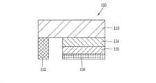
도 4를 참조하면, 상기 반도체 발광소자는 플립 칩 타입(flip chip type)의 발광소자가 될 수 있다.Referring to FIG. 4, the semiconductor light emitting device may be a flip chip type light emitting device.
예를 들어, 상기 반도체 발광소자는 p형 전극(156), p형 전극(156)이 형성되는 p형 반도체층(155), p형 반도체층(155) 상에 형성된 활성층(154), 활성층(154) 상에 형성된 n형 반도체층(153) 및 n형 반도체층(153) 상에서 p형 전극(156)과 수평방향으로 이격 배치되는 n형 전극(152)을 포함한다. 이 경우, p형 전극(156)은 보조전극(170)과 전도성 접착층(130)에 의하여 전기적으로 연결될 수 있고, n형 전극(152)은 제2전극(140)과 전기적으로 연결될 수 있다.For example, the semiconductor light emitting device includes a p-
다시 도 2, 도 3a 및 도 3b를 참조하면, 보조전극(170)은 일방향으로 길게 형성되어, 하나의 보조전극이 복수의 반도체 발광소자(150)에 전기적으로 연결될 수 있다. 예를 들어, 보조전극을 중심으로 좌우의 반도체 발광소자들의 p형 전극들이 하나의 보조전극에 전기적으로 연결될 수 있다.Referring back to FIGS. 2, 3A, and 3B, the
보다 구체적으로, 열 및 압력에 의하여 전도성 접착층(130)의 내부로 반도체 발광소자(150)가 압입되며, 이를 통하여 반도체 발광소자(150)의 p형 전극(156)과 보조전극(170) 사이의 부분과, 반도체 발광소자(150)의 n형 전극(152)과 제2전극(140) 사이의 부분에서만 전도성을 가지게 되고, 나머지 부분에서는 반도체 발광소자의 압입이 없어 전도성을 가지지 않게 된다. 이와 같이, 전도성 접착층(130)은 반도체 발광소자(150)와 보조전극(170) 사이 및 반도체 발광소자(150)와 제2전극(140) 사이를 상호 결합시켜줄 뿐만 아니라 전기적 연결까지 형성시킨다.More specifically, the semiconductor
또한, 복수의 반도체 발광소자(150)는 발광소자 어레이(array)를 구성하며, 발광소자 어레이에는 형광체층(180)이 형성된다.In addition, the plurality of semiconductor
발광소자 어레이는 자체 휘도값이 상이한 복수의 반도체 발광소자들을 포함할 수 있다. 각각의 반도체 발광소자(150)는 단위 화소를 구성하며, 제1전극(120)에 전기적으로 연결된다. 예를 들어, 제1전극(120)은 복수 개일 수 있고, 반도체 발광소자들은 예컨대 수 열로 배치되며, 각 열의 반도체 발광소자들은 상기 복수 개의 제1전극 중 어느 하나에 전기적으로 연결될 수 있다.The light emitting device array may include a plurality of semiconductor light emitting devices having different luminance values. Each semiconductor
또한, 반도체 발광소자들이 플립 칩 형태로 접속되므로, 투명 유전체 기판에 성장시킨 반도체 발광소자들을 이용할 수 있다. 또한, 상기 반도체 발광소자들은 예컨대 질화물 반도체 발광소자일 수 있다. 반도체 발광소자(150)는 휘도가 우수하므로, 작은 크기로도 개별 단위 픽셀을 구성할 수 있다.In addition, since the semiconductor light emitting devices are connected in a flip chip form, semiconductor light emitting devices grown on a transparent dielectric substrate can be used. In addition, the semiconductor light emitting devices may be, for example, nitride semiconductor light emitting devices. Since the semiconductor
도시에 의하면, 반도체 발광소자(150)의 사이에 격벽(190)이 형성될 수 있다. 이 경우, 격벽(190)은 개별 단위 화소를 서로 분리하는 역할을 할 수 있으며, 전도성 접착층(130)과 일체로 형성될 수 있다. 예를 들어, 이방성 전도성 필름에 반도체 발광소자(150)가 삽입됨에 의하여 이방성 전도성 필름의 베이스부재가 상기 격벽을 형성할 수 있다.As illustrated, a
또한, 상기 이방성 전도성 필름의 베이스부재가 블랙이면, 별도의 블랙 절연체가 없어도 상기 격벽(190)이 반사 특성을 가지는 동시에 대비비(contrast)가 증가될 수 있다.In addition, when the base member of the anisotropic conductive film is black, the
다른 예로서, 상기 격벽(190)으로 반사성 격벽이 별도로 구비될 수 있다. 이 경우에, 상기 격벽(190)은 디스플레이 장치의 목적에 따라 블랙(Black) 또는 화이트(White) 절연체를 포함할 수 있다. 화이트 절연체의 격벽을 이용할 경우 반사성을 높이는 효과가 있을 수 있고, 블랙 절연체의 격벽을 이용할 경우, 반사 특성을 가지는 동시에 대비비(contrast)를 증가시킬 수 있다.As another example, a reflective partition wall may be separately provided as the
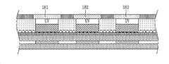
형광체층(180)은 반도체 발광소자(150)의 외면에 위치할 수 있다. 예를 들어, 반도체 발광소자(150)는 청색(B) 광을 발광하는 청색 반도체 발광소자이고, 형광체층(180)은 상기 청색(B) 광을 단위 화소의 색상으로 변환시키는 기능을 수행한다. 상기 형광체층(180)은 개별 화소를 구성하는 적색 형광체(181) 또는 녹색 형광체(182)가 될 수 있다.The
즉, 적색의 단위 화소를 이루는 위치에서, 청색 반도체 발광소자(151) 상에는 청색 광을 적색(R) 광으로 변환시킬 수 있는 적색 형광체(181)가 적층될 수 있고, 녹색의 단위 화소를 이루는 위치에서는, 청색 반도체 발광소자(151) 상에 청색 광을 녹색(G) 광으로 변환시킬 수 있는 녹색 형광체(182)가 적층될 수 있다. 또한, 청색의 단위 화소를 이루는 부분에는 청색 반도체 발광소자(151)만 단독으로 이용될 수 있다. 이 경우, 적색(R), 녹색(G) 및 청색(B)의 단위 화소들이 하나의 화소를 이룰 수 있다. 보다 구체적으로, 제1전극(120)의 각 라인을 따라 하나의 색상의 형광체가 적층될 수 있다. 따라서, 제1전극(120)에서 하나의 라인은 하나의 색상을 제어하는 전극이 될 수 있다. 즉, 제2전극(140)을 따라서, 적색(R), 녹색(G) 및 청색(B)이 차례로 배치될 수 있으며, 이를 통하여 단위 화소가 구현될 수 있다.That is, at a position forming a red unit pixel, a
다만, 본 발명은 반드시 이에 한정되는 것은 아니며, 형광체 대신에 반도체 발광소자(150)와 퀀텀닷(QD)이 조합되어 적색(R), 녹색(G) 및 청색(B)의 단위 화소들을 구현할 수 있다.However, the present invention is not necessarily limited thereto, and unit pixels of red (R), green (G) and blue (B) may be implemented by combining the semiconductor
또한, 대비비(contrast) 향상을 위하여 각각의 형광체층들의 사이에는 블랙 매트릭스(191)가 배치될 수 있다. 즉, 이러한 블랙 매트릭스(191)는 명암의 대조를 향상시킬 수 있다.In addition, a
다만, 본 발명은 반드시 이에 한정되는 것은 아니며, 청색, 적색, 녹색을 구현하기 위한 다른 구조가 적용될 수 있다.However, the present invention is not necessarily limited thereto, and other structures for implementing blue, red, and green colors may be applied.
도 5a를 참조하면, 각각의 반도체 발광소자(150)는 질화 갈륨(GaN)을 주로 하여, 인듐(In) 및/또는 알루미늄(Al)이 함께 첨가되어 청색을 비롯한 다양한 빛을 발광하는 고출력의 발광소자로 구현될 수 있다.Referring to FIG. 5A, each semiconductor
이 경우, 반도체 발광소자(150)는 각각 단위 화소(sub-pixel)를 이루기 위하여 적색, 녹색 및 청색 반도체 발광소자일 수 있다. 예컨대, 적색, 녹색 및 청색 반도체 발광소자(R, G, B)가 교대로 배치되고, 적색, 녹색 및 청색 반도체 발광소자에 의하여 적색(Red), 녹색(Green) 및 청색(Blue)의 단위 화소들이 하나의 화소(pixel)를 이루며, 이를 통하여 풀 칼라 디스플레이가 구현될 수 있다.In this case, the semiconductor
도 5b를 참조하면, 반도체 발광소자는 황색 형광체층이 개별 소자마다 구비된 백색 발광소자(W)를 구비할 수 있다. 이 경우에는, 단위 화소를 이루기 위하여, 백색 발광소자(W) 상에 적색 형광체층(181), 녹색 형광체층(182), 및 청색 형광체층(183)이 구비될 수 있다. 또한, 이러한 백색 발광소자(W) 상에 적색, 녹색, 및 청색이 반복되는 컬러 필터를 이용하여 단위 화소를 이룰 수 있다.Referring to FIG. 5B, the semiconductor light emitting device may include a white light emitting device W in which a yellow phosphor layer is provided for each individual device. In this case, a
도 5c를 참조하면, 자외선 발광소자(UV) 상에 적색 형광체층(181), 녹색 형광체층(182), 및 청색 형광체층(183)이 구비되는 구조도 가능하다. 이와 같이, 반도체 발광소자는 가시광선뿐만 아니라 자외선(UV)까지 전영역에 사용가능하며, 자외선(UV)이 상부 형광체의 여기원(excitation source)으로 사용가능한 반도체 발광소자의 형태로 확장될 수 있다.Referring to FIG. 5C, a structure in which a
본 예시를 다시 살펴보면, 반도체 발광소자(150)는 전도성 접착층(130) 상에 위치되어, 디스플레이 장치에서 단위 화소를 구성한다. 반도체 발광소자(150)는 휘도가 우수하므로, 작은 크기로도 개별 단위 화소를 구성할 수 있다. 이와 같은 개별 반도체 발광소자(150)의 크기는 한 변의 길이가 80㎛ 이하일 수 있고, 직사각형 또는 정사각형 소자일 수 있다. 직사각형인 경우에는 20X80㎛ 이하의 크기가 될 수 있다.Looking again at this example, the semiconductor
또한, 한 변의 길이가 10㎛인 정사각형의 반도체 발광소자(150)를 단위 화소로 이용하여도 디스플레이 장치를 이루기 위한 충분한 밝기가 나타난다. 따라서, 단위 화소의 크기가 한 변이 600㎛, 나머지 한변이 300㎛인 직사각형 화소인 경우를 예로 들면, 반도체 발광소자의 거리가 상대적으로 충분히 크게 된다. 따라서, 이러한 경우, HD화질을 가지는 플렉서블 디스플레이 장치를 구현할 수 있게 된다.In addition, even when a square semiconductor
상기에서 설명된 반도체 발광소자를 이용한 디스플레이 장치는 새로운 형태의 제조방법에 의하여 제조될 수 있다. 이하, 도 6을 참조하여 상기 제조방법에 대하여 설명한다.The display device using the semiconductor light emitting device described above can be manufactured by a new type of manufacturing method. Hereinafter, the manufacturing method will be described with reference to FIG. 6.
도 6은 본 발명의 반도체 발광소자를 이용한 디스플레이 장치의 제조방법을 나타낸 단면도들이다.6 is a cross-sectional view showing a method of manufacturing a display device using the semiconductor light emitting device of the present invention.
본 도면을 참조하면, 먼저, 보조전극(170) 및 제2전극(140)이 위치된 절연층(160) 상에 전도성 접착층(130)을 형성한다. 제1기판(110)에 절연층(160)이 적층되어 하나의 기판(또는 배선기판)을 형성하며, 상기 배선기판에는 제1전극(120), 보조전극(170) 및 제2전극(140)이 배치된다. 이 경우에, 제1전극(120)과 제2전극(140)은 상호 직교 방향으로 배치될 수 있다. 또한, 플렉서블(flexible) 디스플레이 장치를 구현하기 위하여 제1기판(110) 및 절연층(160)은 각각 유리 또는 폴리이미드(PI)를 포함할 수 있다.Referring to this drawing, first, a conductive
상기 전도성 접착층(130)은 예를 들어, 이방성 전도성 필름에 의하여 구현될 수 있으며, 이를 위하여 절연층(160)이 위치된 기판에 이방성 전도성 필름이 도포될 수 있다.The conductive
다음에, 보조전극(170) 및 제2전극(140)들의 위치에 대응하고, 개별 화소를 구성하는 복수의 반도체 발광소자(150)가 위치된 제2기판(112)을 상기 반도체 발광소자(150)가 보조전극(170) 및 제2전극(140)와 대향하도록 배치한다.Next, the
이 경우에, 제2기판(112)은 반도체 발광소자(150)를 성장시키는 성장 기판으로서, 사파이어(spire) 기판 또는 실리콘(silicon) 기판이 될 수 있다.In this case, the
상기 반도체 발광소자는 웨이퍼(wafer) 단위로 형성될 때, 디스플레이 장치를 이룰 수 있는 간격 및 크기를 가지도록 함으로써, 디스플레이 장치에 효과적으로 이용될 수 있다.When the semiconductor light emitting device is formed in units of a wafer, it can be effectively used in a display device by having a gap and a size capable of forming a display device.
그 다음에, 배선기판과 제2기판(112)을 열압착한다. 예를 들어, 배선기판과 제2기판(112)은 ACF press head 를 적용하여 열압착될 수 있다. 상기 열압착에 의하여 배선기판과 제2기판(112)은 본딩(bonding)된다. 열압착에 의하여 전도성을 갖는 이방성 전도성 필름의 특성에 의해 반도체 발광소자(150)와 보조전극(170) 및 제2전극(140)의 사이의 부분만 전도성을 가지게 되며, 이를 통하여 전극들과 반도체 발광소자(150)는 전기적으로 연결될 수 있다. 이 때에, 반도체 발광소자(150)가 상기 이방성 전도성 필름의 내부로 삽입되며, 이를 통하여 반도체 발광소자(150) 사이에 격벽이 형성될 수 있다.Then, the wiring board and the
그 다음에, 상기 제2기판(112)을 제거한다. 예를 들어, 제2기판(112)은 레이저 리프트 오프법(Laser Lift-off, LLO) 또는 화학적 리프트 오프법(Chemical Lift-off, CLO)을 이용하여 제거할 수 있다.Then, the
마지막으로, 상기 제2기판(112)을 제거하여 반도체 발광소자들(150)을 외부로 노출시킨다. 필요에 따라, 반도체 발광소자(150)가 결합된 배선기판 상을 실리콘 옥사이드(SiOx) 등을 코팅하여 투명 절연층(미도시)을 형성할 수 있다.Finally, the
또한, 상기 반도체 발광소자(150)의 일면에 형광체층을 형성하는 단계를 더 포함할 수 있다. 예를 들어, 반도체 발광소자(150)는 청색(B) 광을 발광하는 청색 반도체 발광소자이고, 이러한 청색(B) 광을 단위 화소의 색상으로 변환시키기 위한 적색 형광체 또는 녹색 형광체가 상기 청색 반도체 발광소자의 일면에 레이어를 형성할 수 있다.In addition, a step of forming a phosphor layer on one surface of the semiconductor
이상에서 설명된 반도체 발광소자를 이용한 디스플레이 장치의 제조방법이나 구조는 여러가지 형태로 변형될 수 있다. 그 예로서, 상기에서 설명된 디스플레이 장치에는 수직형 반도체 발광소자도 적용될 수 있다. 이하, 도 5 및 도 6을 참조하여 수직형 구조에 대하여 설명한다.The manufacturing method or structure of a display device using the semiconductor light emitting device described above may be modified in various forms. As an example, a vertical semiconductor light emitting device may also be applied to the display device described above. Hereinafter, a vertical structure will be described with reference to FIGS. 5 and 6.
또한, 이하 설명되는 변형예 또는 실시예에서는 앞선 예와 동일 또는 유사한 구성에 대해서는 동일, 유사한 참조번호가 부여되고, 그 설명은 처음 설명으로 갈음된다.In addition, in the modified examples or embodiments described below, the same or similar reference numerals are assigned to the same or similar configurations as the previous example, and the description is replaced with the first description.
도 7은 발명의 반도체 발광소자를 이용한 디스플레이 장치의 다른 일 실시예를 나타내는 사시도이고, 도 8은 도 7의 라인 D-D를 따라 취한 단면도이며, 도 9은 도 8의 수직형 반도체 발광소자를 나타내는 개념도이다.7 is a perspective view showing another embodiment of a display device using the semiconductor light emitting device of the present invention, FIG. 8 is a cross-sectional view taken along the line DD of FIG. 7, and FIG. 9 is a conceptual diagram showing the vertical semiconductor light emitting device of FIG. to be.
본 도면들을 참조하면, 디스플레이 장치는 패시브 매트릭스(Passive Matrix, PM) 방식의 수직형 반도체 발광소자를 이용한 디스플레이 장치가 될 수 있다.Referring to the drawings, the display device may be a display device using a passive matrix (PM) type vertical semiconductor light emitting device.
상기 디스플레이 장치는 기판(210), 제1전극(220), 전도성 접착층(230), 제2전극(240) 및 복수의 반도체 발광소자(250)를 포함한다.The display device includes a
기판(210)은 제1전극(220)이 배치되는 배선기판으로서, 플렉서블(flexible) 디스플레이 장치를 구현하기 위하여 폴리이미드(PI)를 포함할 수 있다. 이외에도 절연성이 있고, 유연성 있는 재질이면 어느 것이라도 사용 가능할 것이다.The
제1전극(220)은 기판(210) 상에 위치하며, 일 방향으로 긴 바(bar) 형태의 전극으로 형성될 수 있다. 상기 제1전극(220)은 데이터 전극의 역할을 하도록 이루어질 수 있다.The
전도성 접착층(230)은 제1전극(220)이 위치하는 기판(210)상에 형성된다. 플립 칩 타입(flip chip type)의 발광소자가 적용된 디스플레이 장치와 같이, 전도성 접착층(230)은 이방성 전도성 필름(anistropy conductive film, ACF), 이방성 전도 페이스트(paste), 전도성 입자를 함유한 솔루션(solution) 등이 될 수 있다. 다만, 본 실시예에서도 이방성 전도성 필름에 의하여 전도성 접착층(230)이 구현되는 경우를 예시한다.The conductive
기판(210) 상에 제1전극(220)이 위치하는 상태에서 이방성 전도성 필름을 위치시킨 후에, 반도체 발광소자(250)를 열 및 압력을 가하여 접속시키면, 상기 반도체 발광소자(250)가 제1전극(220)과 전기적으로 연결된다. 이 때, 상기 반도체 발광소자(250)는 제1전극(220) 상에 위치되도록 배치되는 것이 바람직하다.After placing the anisotropic conductive film on the
상기 전기적 연결은 전술한 바와 같이, 이방성 전도성 필름에서 열 및 압력이 가해지면 부분적으로 두께방향으로 전도성을 가지기 때문에 생성된다. 따라서, 이방성 전도성 필름에서는 두께방향으로 전도성을 가지는 부분(231)과 전도성을 가지지 않는 부분(232)으로 구획된다.As described above, the electrical connection is created because the anisotropic conductive film partially has conductivity in the thickness direction when heat and pressure are applied. Accordingly, the anisotropic conductive film is divided into a portion 231 having conductivity and a portion 232 having no conductivity in the thickness direction.
또한, 이방성 전도성 필름은 접착 성분을 함유하기 때문에, 전도성 접착층(230)은 반도체 발광소자(250)와 제1전극(220) 사이에서 전기적 연결뿐만 아니라 기계적 결합까지 구현한다.In addition, since the anisotropic conductive film contains an adhesive component, the conductive
이와 같이, 반도체 발광소자(250)는 전도성 접착층(230) 상에 위치되며, 이를 통하여 디스플레이 장치에서 개별 화소를 구성한다. 반도체 발광소자(250)는 휘도가 우수하므로, 작은 크기로도 개별 단위 픽셀을 구성할 수 있다. 이와 같은 개별 반도체 발광소자(250)의 크기는 한 변의 길이가 80㎛ 이하일 수 있고, 직사각형 또는 정사각형 소자일 수 있다. 직사각형인 경우에는 20X80㎛ 이하의 크기가 될 수 있다.In this way, the semiconductor
상기 반도체 발광소자(250)는 수직형 구조가 될 수 있다.The semiconductor
수직형 반도체 발광소자들의 사이에는, 제1전극(220)의 길이 방향과 교차하는 방향으로 배치되고, 수직형 반도체 발광소자(250)와 전기적으로 연결된 복수의 제2전극(240)이 위치한다.A plurality of
도 9를 참조하면, 이러한 수직형 반도체 발광소자는 p형 전극(256), p형 전극(256) 상에 형성된 p형 반도체층(255), p형 반도체층(255) 상에 형성된 활성층(254), 활성층(254)상에 형성된 n형 반도체층(253) 및 n형 반도체층(253) 상에 형성된 n형 전극(252)을 포함한다. 이 경우, 하부에 위치한 p형 전극(256)은 제1전극(220)과 전도성 접착층(230)에 의하여 전기적으로 연결될 수 있고, 상부에 위치한 n형 전극(252)은 후술하는 제2전극(240)과 전기적으로 연결될 수 있다. 이러한 수직형 반도체 발광소자(250)는 전극을 상/하로 배치할 수 있으므로, 칩 사이즈를 줄일 수 있다는 큰 강점을 가지고 있다.Referring to FIG. 9, such a vertical semiconductor light emitting device includes a p-
다시 도 8을 참조하면, 상기 반도체 발광소자(250)의 일면에는 형광체층(280)이 형성될 수 있다. 예를 들어, 반도체 발광소자(250)는 청색(B) 광을 발광하는 청색 반도체 발광소자(251)이고, 이러한 청색(B) 광을 단위 화소의 색상으로 변환시키기 위한 형광체층(280)이 구비될 수 있다. 이 경우에, 형광체층(280)은 개별 화소를 구성하는 적색 형광체(281) 및 녹색 형광체(282) 일 수 있다.Referring back to FIG. 8, a
즉, 적색의 단위 화소를 이루는 위치에서, 청색 반도체 발광소자(251) 상에는 청색 광을 적색(R) 광으로 변환시킬 수 있는 적색 형광체(281)가 적층될 수 있고, 녹색의 단위 화소를 이루는 위치에서는, 청색 반도체 발광소자(251) 상에 청색 광을 녹색(G) 광으로 변환시킬 수 있는 녹색 형광체(282)가 적층될 수 있다. 또한, 청색의 단위 화소를 이루는 부분에는 청색 반도체 발광소자(251)만 단독으로 이용될 수 있다. 이 경우, 적색(R), 녹색(G) 및 청색(B)의 단위 화소들이 하나의 화소를 이룰 수 있다.That is, at a position forming a red unit pixel, a
다만, 본 발명은 반드시 이에 한정되는 것은 아니며, 플립 칩 타입(flip chip type)의 발광소자가 적용된 디스플레이 장치에서 전술한 바와 같이, 청색, 적색, 녹색을 구현하기 위한 다른 구조가 적용될 수 있다.However, the present invention is not necessarily limited thereto, and other structures for implementing blue, red, and green colors may be applied as described above in a display device to which a flip chip type light emitting device is applied.
다시 본 실시예를 살펴보면, 제2전극(240)은 반도체 발광소자들(250) 사이에 위치하고, 반도체 발광소자들(250)과 전기적으로 연결된다. 예를 들어, 반도체 발광소자들(250)은 복수의 열로 배치되고, 제2전극(240)은 반도체 발광소자들(250)의 열들 사이에 위치할 수 있다.Referring back to this embodiment, the
개별 화소를 이루는 반도체 발광소자(250) 사이의 거리가 충분히 크기 때문에 제2전극(240)은 반도체 발광소자들(250) 사이에 위치될 수 있다.Since the distance between the semiconductor
제2전극(240)은 일 방향으로 긴 바(bar) 형태의 전극으로 형성될 수 있으며, 제1전극과 상호 수직한 방향으로 배치될 수 있다.The
또한, 제2전극(240)과 반도체 발광소자(250)는 제2전극(240)에서 돌출된 연결 전극에 의해 전기적으로 연결될 수 있다. 보다 구체적으로, 상기 연결 전극이 반도체 발광소자(250)의 n형 전극이 될 수 있다. 예를 들어, n형 전극은 오믹(ohmic) 접촉을 위한 오믹 전극으로 형성되며, 상기 제2전극은 인쇄 또는 증착에 의하여 오믹 전극의 적어도 일부를 덮게 된다. 이를 통하여 제2전극(240)과 반도체 발광소자(250)의 n형 전극이 전기적으로 연결될 수 있다.In addition, the
도시에 의하면, 상기 제2전극(240)은 전도성 접착층(230) 상에 위치될 수 있다. 경우에 따라, 반도체 발광소자(250)가 형성된 기판(210) 상에 실리콘 옥사이드(SiOx) 등을 포함하는 투명 절연층(미도시)이 형성될 수 있다. 투명 절연층이 형성된 후에 제2전극(240)을 위치시킬 경우, 상기 제2전극(240)은 투명 절연층 상에 위치하게 된다. 또한, 제2전극(240)은 전도성 접착층(230) 또는 투명 절연층에 이격되어 형성될 수도 있다.As illustrated, the
만약 반도체 발광소자(250) 상에 제2전극(240)을 위치시키기 위하여는 ITO(Indium Tin Oxide)와 같은 투명 전극을 사용한다면, ITO 물질은 n형 반도체층과는 접착성이 좋지 않은 문제가 있다. 따라서, 본 발명은 반도체 발광소자(250) 사이에 제2전극(240)을 위치시킴으로써, ITO와 같은 투명 전극을 사용하지 않아도 되는 이점이 있다. 따라서, 투명한 재료 선택에 구속되지 않고, n형 반도체층과 접착성이 좋은 전도성 물질을 수평 전극으로 사용하여 광추출 효율을 향상시킬 수 있다.If a transparent electrode such as ITO (Indium Tin Oxide) is used to place the
도시에 의하면, 반도체 발광소자(250) 사이에는 격벽(290)이 위치할 수 있다. 즉, 개별 화소를 이루는 반도체 발광소자(250)를 격리시키기 위하여 수직형 반도체 발광소자(250) 사이에는 격벽(290)이 배치될 수 있다. 이 경우, 격벽(290)은 개별 단위 화소를 서로 분리하는 역할을 할 수 있으며, 상기 전도성 접착층(230)과 일체로 형성될 수 있다. 예를 들어, 이방성 전도성 필름에 반도체 발광소자(250)가 삽입됨에 의하여 이방성 전도성 필름의 베이스부재가 상기 격벽을 형성할 수 있다.As illustrated, a
또한, 상기 이방성 전도성 필름의 베이스 부재가 블랙이면, 별도의 블랙 절연체가 없어도 상기 격벽(290)이 반사 특성을 가지는 동시에 대비비(contrast)가 증가될 수 있다.In addition, if the base member of the anisotropic conductive film is black, the
다른 예로서, 상기 격벽(190)으로서, 반사성 격벽이 별도로 구비될 수 있다. 격벽(290)은 디스플레이 장치의 목적에 따라 블랙(Black) 또는 화이트(White) 절연체를 포함할 수 있다.As another example, as the
만일 제2전극(240)이 반도체 발광소자(250) 사이의 전도성 접착층(230) 상에 바로 위치된 경우, 격벽(290)은 수직형 반도체 발광소자(250) 및 제2전극(240)의 사이사이에 위치될 수 있다. 따라서, 반도체 발광소자(250)를 이용하여 작은 크기로도 개별 단위 픽셀을 구성할 수 있고, 반도체 발광소자(250)의 거리가 상대적으로 충분히 크게 되어 제2전극(240)을 반도체 발광소자(250) 사이에 위치시킬 수 있고, HD 화질을 가지는 플렉서블 디스플레이 장치를 구현할 수 있는 효과가 있게 된다.If the
또한, 도시에 의하면, 대비비(contrast) 향상을 위하여 각각의 형광체 사이에는 블랙 매트릭스(291)가 배치될 수 있다. 즉, 이러한 블랙 매트릭스(291)는 명암의 대조를 향상시킬 수 있다.Further, according to the illustration, a
상기 설명과 같이, 반도체 발광소자(250)는 전도성 접착층(230) 상에 위치되며, 이를 통하여 디스플레이 장치에서 개별 화소를 구성한다. 반도체 발광소자(250)는 휘도가 우수하므로, 작은 크기로도 개별 단위 픽셀을 구성할 수 있다. 따라서, 반도체 발광소자에 의하여 적색(R), 녹색(G) 및 청색(B)의 단위 화소들이 하나의 화소를 이루는 풀 칼라 디스플레이가 구현될 수 있다.As described above, the semiconductor
상기에서 설명된 본 발명의 반도체 발광소자를 이용한 디스플레이 장치에는 성장기판에서 반도체 발광소자를 분리하기 위해서는 레이저 리프트 오프법(Laser Lift-off, LLO) 또는 화학적 리프트 오프법(Chemical Lift-off, CLO)을 이용하여 분리할 수 있다.In the display device using the semiconductor light emitting device of the present invention described above, in order to separate the semiconductor light emitting device from the growth substrate, a laser lift-off method (LLO) or a chemical lift-off method (CLO). Can be separated by using.
나아가, 성장기판에서 반도체 발광소자를 분리하고 기판 상에 반도체 발광소자를 조립하는 방법으로 스탬프(stamp) 방식, 정전 척(chunk) 방식이 수행될 수 있다. 하지만, 반도체 발광소자를 기판에 조립하는 과정에서 과전사 문제가 발생하게 되어 공정성이 떨어지게 된다는 문제점이 있다. 이에, 본 발명에 의한 디스플레이 장치는 성장기판에서 반도체 발광소자를 분리하여 기판에 조립할 때, 과전사를 방지하고, 공정 속도를 향상시킬 수 있다.Further, as a method of separating the semiconductor light emitting device from the growth substrate and assembling the semiconductor light emitting device on the substrate, a stamp method or an electrostatic chuck method may be performed. However, in the process of assembling the semiconductor light emitting device to the substrate, there is a problem in that an overtransfer problem occurs, resulting in poor fairness. Accordingly, when the semiconductor light emitting device is separated from the growth substrate and assembled to the substrate, the display device according to the present invention can prevent overtransfer and improve the process speed.
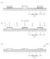
도 10은 새로운 구조의 디스플레이 장치의 본 발명의 다른 실시예를 설명하기 위한, 도 1의 A부분 확대도이다.FIG. 10 is an enlarged view of part A of FIG. 1 for explaining another embodiment of the present invention of a display device having a new structure.
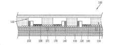
도 10을 참조하면, 디스플레이 장치(1000)는 기판(1001), 제1전극(1020), 절연부재(1030), 제2전극(1040) 및 복수의 반도체 발광소자(1050)를 포함한다. 또한, 디스플레이 장치(1000)는 반도체 발광소자(1050) 상에 배치되는 형광체를 배제하여 단색의 면광원으로 형성될 수 있다.Referring to FIG. 10, the
기판(1001)은 베이스 기판(1010), 절연층(1011) 및 패드(1012) 를 포함할 수 있다. 상세하게, 베이스 기판(1010)은 다양한 재질로 이루어질 수 있으며, 플렉서블(flexible)하거나 또는 인플렉서블(inflexible)하게 이루어질 수 있다. 베이스 기판(1010)이 플렉서블하게 이루어지는 경우, 베이스 기판(1010)은 유리나 폴리이미드(PI, Polyimide)를 포함할 수 있다. 이외에도 절연성이 있고, 유연성 있는 재질이면, 예를 들어 PEN(Polyethylene Naphthalate), PET(Polyethylene Terephthalate) 등 어느 것이라도 사용될 수 있다. 또한, 베이스 기판(1010)은 투명한 재질 또는 불투명한 재질 어느 것이나 될 수 있다. 나아가, 베이스 기판(1010)은 복수의 레이어로 이루어질 수 있다.The
일 실시예에서, 절연층(1011)은 베이스 기판(1010) 상에 배치될 수 있다. 상세하게, 절연층(1011)은 유기소재(1011a) 및 무기입자(1011b)를 포함할 수 있다. 유기소재(1011a)는 실록산 수지, 에폭시 수지 및 아크릴계 수지 중 적어도 하나를 포함할 수 있다.In one embodiment, the insulating
나아가, 무기입자(1011b)는 SiOx, TiOx, AlOx 및 ZnOx 으로 이루어진 군으로부터 적어도 하나 이상 선택될 수 있다. 특히, 무기입자(1011b)는 마이크로 사이즈의 입자로 형성될 수 있다. 또한, 무기입자(1011b)의 적어도 일부는 유기소재(1011a)의 표면으로 드러날 수 있다. 이에, 무기입자(1011b)는 절연층(1011)의 표면으로 돌출되도록 형성될 수 있다.Further, the
한편, 패드(1012)는 절연층(1011)보다 돌출되도록 형성될 수 있다. 또한, 패드(1012) 상에 반도체 발광소자(1050)가 조립될 수 있다. 패드(1012) 상에는 접착력을 가지는 층을 배치하여, 패드(1012) 일면에 반도체 발광소자(1050)를 고정시킬 수 있다. 또한, 패드(1012)는 접착력을 가져 추가로 배치되는 층 없이도 반도체 발광소자(1050)를 고정시킬 수도 있다.Meanwhile, the
도시와 같이 디스플레이 장치(1000)을 형성하는 반도체 발광소자(1050)가 플립 칩 타입의 반도체 발광소자일 경우에는 패드(1012)는 절연성을 가지는 실록산 수지, 에폭시 수지 및 아크릴계 수지 중 적어도 하나를 포함할 수 있다. 한편, 상기 디스플레이 장치를 형성하는 반도체 발광소자가 수직형 반도체 발광소자일 경우에는 패드는 도전성 소재로 형성되어 전극의 역할을 수행할 수도 있다. 이는 후술되는 도 15에서 상세하게 설명한다.As shown in the figure, when the semiconductor
다시 도면을 참조하면, 절연층(1011)과 패드(1012)는 서로 상이한 거칠기의 표면을 가질 수 있다. 일 실시예에서, 무기입자(1011b)의 적어도 일부가 돌출되도록 형성된 절연층(1011)의 표면의 거칠기가 패드(1012)의 표면보다 더 큰 거칠기를 가지도록 형성될 수 있다. 이에, 반도체 발광소자(1050)가 조립되는 과정에서 절연층(1011)과 패드(1012)의 표면에서 선택적으로 조립을 형성할 수 있다.Referring back to the drawings, the insulating
상세하게, 거칠기가 더 큰 절연층(1011)의 표면에서는 반도체 발광소자(1050)의 조립이 어려워진다. 따라서, 절연층(1011) 상에 반도체 발광소자(1050)가 과전사되는 문제점이 해결될 수 있다. 특히, 패드(1012)는 절연층(1011)보다 돌출되도록 형성되므로, 물리적인 접촉으로 반도체 발광소자(1050)가 접합할 때에도, 패드(1012)와 반도체 발광소자(1050)가 서로 접촉하더라도, 절연층(1011)과 반도체 발광소자(1050) 상에는 간극이 발생한다. 따라서, 절연층(1011)과 반도체 발광소자(1050)의 접합이 방지될 수 있으므로 절연층(1011) 상에 반도체 발광소자(1050)가 과전사되는 것을 방지할 수 있는 효과가 있다.In detail, it becomes difficult to assemble the semiconductor
한편, 기판(1001)은 절연층(1011)에 리세스된 홈을 구비하고 상기 패드가 리세스된 홈에 배치되는 형태도 가능하다. 이는 후술되는 도 12에서 상세하게 설명한다.Meanwhile, the
한편, 반도체 발광소자(1050)는 제1도전형 반도체층(1053), 활성층(1054) 및 제2도전형 반도체층(1055)을 포함할 수 있다. 또한, 반도체 발광소자(1050)는 제1도전형 반도체층(1053)의 일면상에 형성되는 제1도전형 전극(1052) 및 제2도전형 반도체층(1055)의 일면상에 형성되는 제2도전형 전극(1056)을 포함하도록 형성될 수 있다.Meanwhile, the semiconductor
보다 구체적으로, 제1도전형 반도체층(1053) 및 제1도전형 전극(1052)은 각각 p형 전극 및 p형 반도체층이 될 수 있으며, 제2도전형 반도체층(1055)은 각각 n형 전극 및 n형 반도체층이 될 수 있다. 다만, 본 발명은 반드시 이에 한정되는 것은 아니며, 제1도전형이 n형이 되고 제2도전형이 p형이 되는 예시도 가능하다.More specifically, the first conductive
일 실시예에서, 절연부재(1030) 반도체 발광소자(1050)를 감싸도록 형성될 수 있다. 일 실시예에서, 절연부재(1030)는 고분자 소재로 폴리디메틸실록산(Polydimethylsiloxane, PDMS) 또는 폴리메틸페닐실록산(polymethylphenylsiloxane, PMPS)을 포함할 수 있으며, 반도체 발광소자(1050)를 감싸며, 절연성을 가지는 다양한 소재를 포함할 수 있다.In one embodiment, the insulating
한편, 절연부재(1030) 상에는 제1전극(1020) 및 제2전극(1040)이 배치될 수 있다. 상세하게, 반도체 발광소자(1050)의 제1도전형 전극(1056) 및 제2도전형 전극(1052)은 각각 제1전극(1020) 및 제2전극(1040)에 대응되어 전기적으로 결합될 수 있다.Meanwhile, a
도 11은 본 발명의 디스플레이 장치(1000)의 절연층(1011) 및 패드(1012)를 포함하는 기판(1001)의 제조방법을 나타내는 개념도들이다.11 is a conceptual diagram illustrating a method of manufacturing a
도 11의 (a)를 참조하면, 베이스 기판(1010) 상에 유기소재(1011a) 및 무기입자(1011b)를 포함하는 절연층(1011')을 형성하고, 절연층(1011')에 돌출된 패드(1012)를 형성할 수 있다. 나아가, 패드(1012) 상에 패드보호층(1013')을 형성한다.Referring to FIG. 11A, an insulating layer 1011' including an
도 11의 (b)를 참조하면, 절연층(1011') 및 패드보호층(1013')의 표면을 식각하는 공정을 수행하고, 식각하는 공정은 바람직하게는 드라이에칭(dry etching)으로 수행될 수 있다. 이에, 절연층(1011')은 식각되며, 표면으로 무기입자(1011b)의 적어도 일부가 돌출되도록 형성되는 절연층(1011)이 형성된다.Referring to (b) of FIG. 11, a process of etching the surfaces of the insulating layer 1011' and the pad protection layer 1013' is performed, and the etching process is preferably performed by dry etching. I can. Accordingly, the insulating
도 11의 (c)를 참조하면, 식각이 수행된 패드보호층(1013)이 제거되어 기판(1001)이 형성될 수 있다.Referring to FIG. 11C, the
도 12는 본 발명의 디스플레이 장치(1000)의 절연층(1011) 및 패드(1012)를 포함하는 또 다른 기판(1001a)의 제조방법을 나타내는 개념도들이다. 이하 설명되는 기판(1001a)의 제조방법에서는 앞선 실시예와 동일 또는 유사한 구성에 대해서는 동일, 유사한 참조번호가 부여되고, 그 설명은 처음 설명으로 갈음된다.12 is a conceptual diagram showing a method of manufacturing another
도 12의 (a)를 참조하면, 베이스 기판(1010) 상에 유기소재(1011a) 및 무기입자(1011b)를 포함하는 절연층(1011')을 형성하고, 절연층(1011')의 적어도 일부를 제거하여 베이스 기판(1010)을 향하여 리세스된 홈을 형성할 수 있다. 이어서, 리세스된 홈에 패드(1012a)를 형성하되, 패드(1012a)는 절연층(1011')보다 돌출되도록 형성한다. 패드(1012a) 상에 패드보호층(1013')을 형성한다.Referring to FIG. 12A, an insulating layer 1011' including an
도 12의 (b)를 참조하면, 절연층(1011') 및 패드보호층(1013')의 표면을 식각하는 공정을 수행하고, 식각하는 공정은 바람직하게는 드라이에칭(dry etching)으로 수행될 수 있다. 이에, 절연층(1011')은 식각되며, 표면으로 무기입자(1011b)의 적어도 일부가 돌출되도록 형성되는 절연층(1011)이 형성된다.Referring to FIG. 12B, a process of etching the surfaces of the insulating layer 1011' and the pad protection layer 1013' is performed, and the etching process is preferably performed by dry etching. I can. Accordingly, the insulating
도 12의 (c)를 참조하면, 식각이 수행된 패드보호층(1013)이 제거되어 기판(1001a)이 형성될 수 있다.Referring to FIG. 12C, the
도 13는 스탬프 방식을 통한 본 발명에 따른 디스플레이 장치(1000)의 제조방법을 나타내는 개념도들이다.13 is a conceptual diagram illustrating a method of manufacturing the
도 13을 참조하면, 베이스 기판(1010), 절연층(1011) 및 패드(1012)를 포함하는 기판(1001)에 반도체 발광소자(1050')가 조립될 수 있다.Referring to FIG. 13, a semiconductor
도 13의 (a)를 참조하면, 반도체 발광소자(1050')는 성장기판(W) 상에 적층되고, 식각과 같은 공정을 통하여 형성될 수 있다. 나아가, 반도체 발광소자(1050')은 식각공정에 의하여 형성된 앵커구조(1060)를 포함할 수 있다.Referring to FIG. 13A, the semiconductor
반도체 발광소자(1050')는 베이스 기판(1010), 절연층(1011) 및 패드(1012)를 포함하는 기판에 스탬핑되어 앵커구조(1060)에서 분리되어 전사 또는 조립될 수 있다.The semiconductor
이때, 거칠기가 더 큰 절연층(1011)의 표면에서는 반도체 발광소자(1050')의 조립이 어려우므로 절연층(1011) 상에 반도체 발광소자(1050')가 과전사되는 문제점이 해결될 수 있다. 특히, 패드(1012)는 절연층(1011)보다 돌출되도록 형성되므로, 물리적인 접촉으로 반도체 발광소자(1050')가 접합할 때에도, 패드(1012)와 반도체 발광소자(1050')가 서로 접촉하더라도, 절연층(1011)과 반도체 발광소자(1050') 상에는 간극이 발생한다. 따라서, 절연층(1011)과 반도체 발광소자(1050')의 접촉이 방지될 수 있으므로 절연층(1011) 상에 반도체 발광소자(1050')가 과전사되는 것을 방지할 수 있다.At this time, since it is difficult to assemble the semiconductor
도 13의 (b)를 참조하면, 반도체 발광소자(1050')가 성장기반(W)으로부터 분리되고 패드(1012) 상에 조립된 다음 제1도전형 전극(1052) 및 제2도전형 전극(1056)을 형성하여, 제1도전형 전극(1052) 및 제2도전형 전극(1056)이 구비된 반도체 발광소자(1050)를 형성될 수 있다.13B, the semiconductor light emitting device 1050' is separated from the growth base W and assembled on the
도 13의 (c)를 참조하면, 반도체 발광소자(1050)를 감싸는 절연층(1030)을 형성하고 제1전극(1020) 및 제2전극(1040)을 형성하여 디스플레이 장치(1000)를 제조할 수 있다.Referring to FIG. 13C, an insulating
도 14는 도너기판(W')을 통한 본 발명에 따른 디스플레이 장치(1000)의 제조방법을 나타내는 개념도들이다.14 is a conceptual diagram illustrating a method of manufacturing a
도 14를 참조하면, 디스플레이 장치(1000)는 전술된 성장기판 상에서 제조된 반도체 발광소자(1050)를 도너기판(W')으로 전사한 후에 반도체 발광소자(1050)들 중 일부를 선택적으로 베이스 기판(1010), 절연층(1011) 및 패드(1012)를 포함하는 기판에 조립시켜 형성할 수 있다.Referring to FIG. 14, after transferring the semiconductor
도 14의 (a)를 참조하면, 도너기판(W')은 탄성을 가지는 외력에 의하여 변형될 수 있는 재질로 형성될 수 있다. 즉, 도너기판(W')이 상기 기판에 압력에 의하여 접촉하며 반도체 발광소자(1050)가 전사될 때, 정전기력, 반데르발스 힘(van der Waals force)에 의하여 과전사될 수 있다.Referring to FIG. 14A, the donor substrate W'may be formed of a material that can be deformed by an external force having elasticity. That is, when the donor substrate W'contacts the substrate by pressure and the semiconductor
하지만, 도 14의 (a)에서는 거칠기가 더 큰 절연층(1011)의 표면에서는 반도체 발광소자(1050)의 조립이 어려우므로 절연층(1011) 상에 반도체 발광소자(1050)가 과전사되는 문제점이 해결될 수 있다. 특히, 패드(1012)는 절연층(1011)보다 돌출되도록 형성되므로, 물리적인 접촉으로 반도체 발광소자(1050)가 접합할 때에도, 패드(1012)와 반도체 발광소자(10500)가 서로 접촉하더라도, 절연층(1011)과 반도체 발광소자(1050) 상에는 간극이 발생한다. 따라서, 절연층(1011)과 반도체 발광소자(1050)의 접촉이 방지될 수 있으므로 절연층(1011) 상에 반도체 발광소자(1050)가 과전사되는 것을 방지할 수 있다.However, in (a) of FIG. 14, it is difficult to assemble the semiconductor
한편, 반도체 발광소자(1050)이 분리되어 패드(1012)에 배치되는 공정은 전술된 것과 같이 도너기판(W')을 이용한 전사방법으로 수행될 수 있으며, 성장기판에서 반도체 발광소자가 바로 분리되는 레이저 리프트 오프법(Laser Lift-off, LLO) 또는 화학적 리프트 오프법(Chemical Lift-off, CLO)을 이용하여 전사될 수 있다.Meanwhile, the process in which the semiconductor
도 14의 (b)를 참조하면, 전술한 다양한 전사방법으로 패드(1012)에 배치된 반도체 발광소자(1050)를 형성될 수 있다.Referring to FIG. 14B, the semiconductor
도 14의 (c)를 참조하면, 반도체 발광소자(1050)를 감싸는 절연층(1030)을 형성하고 제1전극(1020) 및 제2전극(1040)을 형성하여 디스플레이 장치(1000)를 제조할 수 있다.Referring to FIG. 14C, an insulating
전술된 도 13 및 도 14에서 사용되는 기판은 도 12에서 설명된 상기 절연층에 리세스된 홈을 구비하고 상기 패드가 형성된 기판(1001a)가 사용될 수도 있다.The substrate used in FIGS. 13 and 14 described above may include a
도 15는 새로운 구조의 디스플레이 장치(2000)가 적용된 본 발명의 또 다른 실시 예를 설명하기 위한, 도 1의 A부분 확대도이다. 이하 설명되는 디스플레이 장치(2000)에서는 앞선 실시예와 동일 또는 유사한 구성에 대해서는 동일, 유사한 참조번호가 부여되고, 그 설명은 처음 설명으로 갈음된다.FIG. 15 is an enlarged view of portion A of FIG. 1 for explaining another embodiment of the present invention to which a new structure of the
도 15를 참조하면, 디스플레이 장치(2000)를 형성하는 반도체 발광소자는 수직형 반도체 발광소자(2050)으로 형성될 수 있다. 이에, 패드(2012)는 도전성 소재로 형성되어 전극의 역할을 수행할 수도 있다.Referring to FIG. 15, a semiconductor light emitting device forming the
또한, 디스플레이 장치(2000)는, 복수의 반도체 발광소자(2050)의 일면에 형성되는 형광체층(2080)을 더 구비할 수 있다. 예를 들어, 반도체 발광소자(2050)는 청색(B) 광을 발광하는 청색 반도체 발광소자이고, 형광체층(2080)은 상기 청색(B) 광을 단위 화소의 색상으로 변환시키는 기능을 수행한다. 형광체층(2080)은 개별 화소를 구성하는 적색 형광체(2081) 또는 녹색 형광체(2082)가 될 수 있다. 또한, 형광체층(2080)의 대비비(Contrast) 향상을 위하여 디스플레이 장치는 각각의 형광체들의 사이에 배치되는 블랙 매트릭스(2091)를 더 포함할 수 있다.In addition, the
일 실시예에서, 반도체 발광소자(2050)들의 제1도전형 전극(2056) 및 제2도전형 전극(2052)은 각각 제1전극(2020) 및 제2전극(2040)에 대응되어 전기적으로 결합될 수 있다.In one embodiment, the first
상세하게, 절연층(2011) 상에 배선(미도시)이 형성되어 반도체 발광소자(2050)들 간의 연결을 형성할 수 있다. 이에, 제2도전형 전극(2056)에 대응되는 패드(2012)는 AuSn, InSn 및 In 으로 이루어진 군으로부터 선택될 수 있다. 이에, 상기 배선과 반도체 발광소자(2050)의 전기적 연결이 형성될 수 있다. 나아가, 반도체 발광소자(2050)의 하부에 패드(2012)가 배치되므로 열 전도도가 우수한 AuSn, InSn 및 In 으로 이루어진 군으로부터 선택되어 형성된 패드(2012)는 디스플레이 장치(2000)의 방열성능을 향상시킬 수도 있다. AuSn, InSn 및 In 으로 이루어진 군으로부터 선택되어 형성된 패드(2012)는 공정에 따라서 스스로 접착력을 가질 수 있으므로 추가로 배치되는 층 없이도 반도체 발광소자(2050)를 패드(2012) 상에 고정시킬 수도 있다.In detail, a wiring (not shown) may be formed on the insulating
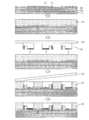
도 16은 본 발명의 실시예와 비교예의 반도체 발광소자 과전사 테스트 시험의 결과를 이미지로 나타내었다.16 shows the results of the semiconductor light-emitting device overtransfer test test of Examples and Comparative Examples of the present invention as images.
도 16의 (a)는 실시예의 반도체 발광소자 과전사 테스트 실험의 예이다. 도 16의 (a)에서는 패드를 형성하지 않았고, 베이스 기판에 무기입자의 일부가 돌출된 절연층을 형성하고, 반도체 발광소자를 전사시켜 과전사 여부를 실험하였다. 이에, 드라이에칭을 통한 상기 절연층 표면의 거칠기 증가로 이미지상 어둡게 나타났으나, 과전사 테스트 결과 상기 절연층 상에 과전사된 상기 반도체 발광소자는 나타나지 않았다.16A is an example of an overtransfer test experiment of the semiconductor light emitting device of the embodiment. In FIG. 16A, a pad was not formed, and an insulating layer in which some of the inorganic particles protruded was formed on the base substrate, and the semiconductor light emitting device was transferred to test whether overtransfer was performed. Accordingly, the image appeared dark due to an increase in the roughness of the surface of the insulating layer through dry etching, but the semiconductor light emitting device overtransferred onto the insulating layer was not found as a result of an overtransfer test.
한편, 도 16의 (b)는 비교예의 반도체 발광소자 과전사 테스트 실험의 예이다. 도 16의 (b)에서는 패드는 형성하지 않고, 베이스 기판에 무기입자를 포함하는 절연층을 형성하였으나, 드라이에칭은 수행하지 않았다. 실험 결과를 살펴보면, 상기 반도체 발광소자가 절연층 상에 과전사 된 것이 나타난 것을 알 수 있다.Meanwhile, FIG. 16B is an example of a semiconductor light emitting device overtransfer test experiment of a comparative example. In FIG. 16B, a pad was not formed and an insulating layer including inorganic particles was formed on the base substrate, but dry etching was not performed. Looking at the experimental results, it can be seen that the semiconductor light emitting device is overtransferred onto the insulating layer.
따라서, 본 발명의 기판이 적용된 실시예에서는 반도체 발광소자를 조립하는 과정에서 과전사 불량이 개선될 수 있다는 것을 알 수 있다.Accordingly, in the embodiment to which the substrate of the present invention is applied, it can be seen that the overtransfer defect can be improved in the process of assembling the semiconductor light emitting device.
이상에서 설명한 반도체 발광소자를 이용한 디스플레이 장치는 위에서 설명된 실시예들의 구성과 방법에 한정되는 것이 아니라, 상기 실시예들은 다양한 변형이 이루어질 수 있도록 각 실시예들의 전부 또는 일부가 선택적으로 조합되어 구성될 수도 있다.The display device using the semiconductor light emitting device described above is not limited to the configuration and method of the embodiments described above, but the embodiments are configured by selectively combining all or part of each embodiment so that various modifications can be made. May be.
Claims (11)
Translated fromKorean상기 기판은,
베이스 기판;
상기 베이스 기판 상에 구비된 절연층; 및
상기 절연층보다 돌출되도록 형성되고 상기 반도체 발광소자가 조립되도록 형성되는 패드를 포함하고,
상기 절연층은 무기입자를 포함하고, 상기 무기입자의 적어도 일부는 상기 절연층의 표면으로 돌출되도록 형성되며,
상기 패드는 실록산 수지, 에폭시 수지 및 아크릴계 수지 중 적어도 하나를 포함하며,
상기 패드에 조립되는 상기 반도체 발광소자는, 제1 도전형 전극, 상기 제1 도전형 전극이 형성되는 제1 도전형 반도체층, 상기 제1 도전형 반도체층 상에 형성된 활성층, 상기 활성층 상에 형성된 제2 도전형 반도체층 및 상기 제2 도전형 반도체층 상에서 상기 제1 도전형 전극과 수평 방향으로 이격 배치되는 제2 도전형 전극을 포함하는 것을 특징으로 하는, 디스플레이 장치.In a display device having a plurality of semiconductor light emitting elements on a substrate,
The substrate,
A base substrate;
An insulating layer provided on the base substrate; And
And a pad formed to protrude from the insulating layer and formed to assemble the semiconductor light emitting device,
The insulating layer includes inorganic particles, and at least a portion of the inorganic particles is formed to protrude to the surface of the insulating layer,
The pad includes at least one of a siloxane resin, an epoxy resin, and an acrylic resin,
The semiconductor light emitting device assembled on the pad includes a first conductivity type electrode, a first conductivity type semiconductor layer on which the first conductivity type electrode is formed, an active layer formed on the first conductivity type semiconductor layer, and the active layer. A display device comprising: a second conductivity type semiconductor layer and a second conductivity type electrode disposed horizontally apart from the first conductivity type electrode on the second conductivity type semiconductor layer.
상기 절연층은, 실록산 수지, 에폭시 수지 및 아크릴계 수지 중 적어도 하나를 포함하는 것을 특징으로 하는 디스플레이 장치.The method of claim 1,
The insulating layer, a display device comprising at least one of a siloxane resin, an epoxy resin, and an acrylic resin.
상기 무기입자는 SiOx, TiOx, AlOx 및 ZnOx 으로 이루어진 군으로부터 적어도 하나 이상 선택되는 것을 특징으로 하는 디스플레이 장치.The method of claim 1,
The inorganic particle is a display device, characterized in that at least one selected from the group consisting of SiOx, TiOx, AlOx, and ZnOx.
상기 절연층은 상기 베이스 기판을 향하여 리세스된 홈을 구비하고,
상기 패드는 상기 리세스된 홈에 배치되는 것을 특징으로 하는 디스플레이 장치.The method of claim 1,
The insulating layer has a groove recessed toward the base substrate,
The display device, wherein the pad is disposed in the recessed groove.
베이스 기판 상에 무기입자를 포함하는 절연층을 형성하는 단계;
상기 절연층보다 돌출된 패드를 형성하는 단계;
상기 패드 상에 패드보호층을 형성하는 단계;
상기 절연층을 식각하여 상기 무기입자가 표면으로 돌출된 절연층을 형성하는 단계; 및
상기 패드보호층을 제거하고, 상기 패드 상에 반도체 발광소자를 조립하는 단계를 포함하는 것을 특징으로 하는 디스플레이 장치의 제조방법.In the manufacturing method of the display device,
Forming an insulating layer including inorganic particles on the base substrate;
Forming a pad protruding from the insulating layer;
Forming a pad protection layer on the pad;
Etching the insulating layer to form an insulating layer in which the inorganic particles protrude to a surface; And
And removing the pad protection layer and assembling a semiconductor light emitting device on the pad.
상기 절연층을 형성하는 단계에서 상기 절연층은 실록산 수지, 에폭시 수지 및 아크릴계 수지 중 적어도 하나를 포함하는 것을 특징으로 하는 디스플레이 장치의 제조방법.The method of claim 7,
In the step of forming the insulating layer, the insulating layer comprises at least one of a siloxane resin, an epoxy resin, and an acrylic resin.
상기 절연층을 형성하는 단계에서 상기 무기입자는 SiOx, TiOx, AlOx 및 ZnOx 으로 이루어진 군으로부터 적어도 하나 이상 선택되는 것을 특징으로 하는 디스플레이 장치의 제조방법.The method of claim 7,
In the step of forming the insulating layer, the inorganic particles are at least one selected from the group consisting of SiOx, TiOx, AlOx, and ZnOx.
상기 절연층을 형성하는 단계와 상기 패드를 형성하는 단계 사이에 상기 절연층의 적어도 일부를 제거하여 상기 베이스 기판을 향하여 리세스된 홈을 형성하는 단계를 더 포함하는 것을 특징으로 하는 디스플레이 장치의 제조방법.The method of claim 7,
And forming a recessed groove toward the base substrate by removing at least a portion of the insulating layer between the step of forming the insulating layer and the step of forming the pad. Way.
상기 리세스된 홈에 상기 패드를 형성하는 것을 특징으로 하는 디스플레이 장치의 제조방법.The method of claim 10,
And forming the pad in the recessed groove.
Priority Applications (4)
| Application Number | Priority Date | Filing Date | Title |
|---|---|---|---|
| KR1020180080713AKR102193700B1 (en) | 2018-07-11 | 2018-07-11 | Display device using semiconductor light emitting device |
| PCT/KR2018/009957WO2020013379A1 (en) | 2018-07-11 | 2018-08-29 | Display device using semiconductor light-emitting elements |
| EP18926241.3AEP3823029B1 (en) | 2018-07-11 | 2018-08-29 | Display device using semiconductor light-emitting elements |
| US17/259,084US20210320146A1 (en) | 2018-07-11 | 2018-08-29 | Display device using semiconductor light-emitting elements |
Applications Claiming Priority (1)
| Application Number | Priority Date | Filing Date | Title |
|---|---|---|---|
| KR1020180080713AKR102193700B1 (en) | 2018-07-11 | 2018-07-11 | Display device using semiconductor light emitting device |
Publications (2)
| Publication Number | Publication Date |
|---|---|
| KR20200006843A KR20200006843A (en) | 2020-01-21 |
| KR102193700B1true KR102193700B1 (en) | 2020-12-21 |
Family
ID=69141777
Family Applications (1)
| Application Number | Title | Priority Date | Filing Date |
|---|---|---|---|
| KR1020180080713AActiveKR102193700B1 (en) | 2018-07-11 | 2018-07-11 | Display device using semiconductor light emitting device |
Country Status (4)
| Country | Link |
|---|---|
| US (1) | US20210320146A1 (en) |
| EP (1) | EP3823029B1 (en) |
| KR (1) | KR102193700B1 (en) |
| WO (1) | WO2020013379A1 (en) |
Cited By (1)
| Publication number | Priority date | Publication date | Assignee | Title |
|---|---|---|---|---|
| WO2024005341A1 (en)* | 2022-06-29 | 2024-01-04 | 삼성전자주식회사 | Connection structure between light emitting diode and substrate, and display module including same |
Families Citing this family (1)
| Publication number | Priority date | Publication date | Assignee | Title |
|---|---|---|---|---|
| CN112965305B (en)* | 2020-07-08 | 2023-11-17 | 友达光电股份有限公司 | display panel |
Citations (1)
| Publication number | Priority date | Publication date | Assignee | Title |
|---|---|---|---|---|
| JP2012227293A (en)* | 2011-04-18 | 2012-11-15 | Ibiden Co Ltd | Solder resist, solder resist raw material, led substrate, light-emitting module, apparatus with light-emitting module, manufacturing method for led substrate, manufacturing method for light-emitting module, and manufacturing method for apparatus with light-emitting module |
Family Cites Families (13)
| Publication number | Priority date | Publication date | Assignee | Title |
|---|---|---|---|---|
| JP4772395B2 (en)* | 2005-06-24 | 2011-09-14 | 三菱電機株式会社 | Electro-optic display device and manufacturing method thereof |
| US8110839B2 (en)* | 2009-07-13 | 2012-02-07 | Luxingtek, Ltd. | Lighting device, display, and method for manufacturing the same |
| WO2012105180A1 (en)* | 2011-01-31 | 2012-08-09 | シャープ株式会社 | Liquid crystal display panel, production method for same, and array substrate and production method for same |
| JP5456209B2 (en)* | 2011-08-01 | 2014-03-26 | 株式会社Steq | Semiconductor device and manufacturing method thereof |
| WO2014140796A1 (en)* | 2013-03-15 | 2014-09-18 | Cooledge Lighting, Inc. | Wafer-level flip chip device packages and related methods |
| US8987765B2 (en)* | 2013-06-17 | 2015-03-24 | LuxVue Technology Corporation | Reflective bank structure and method for integrating a light emitting device |
| JP6119490B2 (en)* | 2013-07-31 | 2017-04-26 | ソニー株式会社 | Light source device and display device |
| KR102385229B1 (en)* | 2014-10-13 | 2022-04-12 | 삼성디스플레이 주식회사 | Pad electrode structure, flat display apparatus comprising the pad electrode structure and the method of manufacturing the same |
| KR102446768B1 (en)* | 2015-12-14 | 2022-09-23 | 엘지전자 주식회사 | Display device using semiconductor light emitting device and manufacturing method thereof |
| JP6418200B2 (en)* | 2016-05-31 | 2018-11-07 | 日亜化学工業株式会社 | Light emitting device and manufacturing method thereof |
| KR20180033645A (en)* | 2016-09-26 | 2018-04-04 | 주성엔지니어링(주) | Thin film transistor substrate |
| KR101947643B1 (en)* | 2016-12-02 | 2019-02-13 | 엘지전자 주식회사 | Display device using semiconductor light emitting device |
| KR102551580B1 (en)* | 2016-12-30 | 2023-07-04 | 엘지디스플레이 주식회사 | Array substrate for display device and display device having the same |
- 2018
- 2018-07-11KRKR1020180080713Apatent/KR102193700B1/enactiveActive
- 2018-08-29USUS17/259,084patent/US20210320146A1/enactivePending
- 2018-08-29EPEP18926241.3Apatent/EP3823029B1/enactiveActive
- 2018-08-29WOPCT/KR2018/009957patent/WO2020013379A1/ennot_activeCeased
Patent Citations (1)
| Publication number | Priority date | Publication date | Assignee | Title |
|---|---|---|---|---|
| JP2012227293A (en)* | 2011-04-18 | 2012-11-15 | Ibiden Co Ltd | Solder resist, solder resist raw material, led substrate, light-emitting module, apparatus with light-emitting module, manufacturing method for led substrate, manufacturing method for light-emitting module, and manufacturing method for apparatus with light-emitting module |
Cited By (1)
| Publication number | Priority date | Publication date | Assignee | Title |
|---|---|---|---|---|
| WO2024005341A1 (en)* | 2022-06-29 | 2024-01-04 | 삼성전자주식회사 | Connection structure between light emitting diode and substrate, and display module including same |
Also Published As
| Publication number | Publication date |
|---|---|
| WO2020013379A1 (en) | 2020-01-16 |
| US20210320146A1 (en) | 2021-10-14 |
| EP3823029C0 (en) | 2023-06-28 |
| EP3823029A1 (en) | 2021-05-19 |
| EP3823029B1 (en) | 2023-06-28 |
| KR20200006843A (en) | 2020-01-21 |
| EP3823029A4 (en) | 2022-04-13 |
Similar Documents
| Publication | Publication Date | Title |
|---|---|---|
| CN105051804B (en) | Display device using semiconductor light emitting device | |
| KR102728384B1 (en) | Display device using micro-led and manufacturing method thereof | |
| KR101620469B1 (en) | Fabricating method of display apparatus using semiconductor light emitting device | |
| KR20190104277A (en) | Display device using micro led and manufacturing method thereof | |
| CN105830141A (en) | Display device using semiconductor light emitting device and manufacturing method thereof | |
| KR102227086B1 (en) | Display device using semiconductor light emitting device | |
| CN107210292B (en) | Display device using semiconductor light-emitting device and method of manufacturing the same | |
| KR20200002733A (en) | Display device using light emitting device and manufacturing method thereof | |
| CN106062858A (en) | Display device using semiconductor light emitting device | |
| KR102205693B1 (en) | Display device using semiconductor light emitting device | |
| KR102502970B1 (en) | Manufacturing method and display device of a display device using a semiconductor light emitting device | |
| KR102744633B1 (en) | Display device using micro led | |
| KR102357645B1 (en) | Display device using semiconductor light emitting device | |
| KR20200104876A (en) | Display device using semiconductor light emitting device | |
| KR102766068B1 (en) | Semiconductor light-emitting device and display device using semiconductor light-emitting device | |
| US12382761B2 (en) | Display device using a semiconductor light emitting device and manufacturing method thereof | |
| KR102803811B1 (en) | Display device using semiconductor light emitting device and method for manufacturing | |
| KR20160074336A (en) | Display device using semiconductor light emitting device | |
| KR102193700B1 (en) | Display device using semiconductor light emitting device | |
| US20230017298A1 (en) | Display apparatus using semiconductor light emitting device and method for manufacturing same | |
| KR20180135335A (en) | Display device using semiconductor light emitting device | |
| KR102456888B1 (en) | Display device using semiconductor light emitting device | |
| KR20200005096A (en) | Display device using semiconductor light emitting device and method for manufacturing | |
| KR102546499B1 (en) | Display device using semiconductor light emitting device | |
| US12284844B2 (en) | Display device using semiconductor light-emitting elements and method for manufacturing same |
Legal Events
| Date | Code | Title | Description |
|---|---|---|---|
| A201 | Request for examination | ||
| PA0109 | Patent application | Patent event code:PA01091R01D Comment text:Patent Application Patent event date:20180711 | |
| PA0201 | Request for examination | ||
| E902 | Notification of reason for refusal | ||
| PE0902 | Notice of grounds for rejection | Comment text:Notification of reason for refusal Patent event date:20190924 Patent event code:PE09021S01D | |
| PG1501 | Laying open of application | ||
| E90F | Notification of reason for final refusal | ||
| PE0902 | Notice of grounds for rejection | Comment text:Final Notice of Reason for Refusal Patent event date:20200304 Patent event code:PE09021S02D | |
| E701 | Decision to grant or registration of patent right | ||
| PE0701 | Decision of registration | Patent event code:PE07011S01D Comment text:Decision to Grant Registration Patent event date:20200925 | |
| GRNT | Written decision to grant | ||
| PR0701 | Registration of establishment | Comment text:Registration of Establishment Patent event date:20201215 Patent event code:PR07011E01D | |
| PR1002 | Payment of registration fee | Payment date:20201216 End annual number:3 Start annual number:1 | |
| PG1601 | Publication of registration | ||
| PR1001 | Payment of annual fee | Payment date:20231109 Start annual number:4 End annual number:4 |