KR102192393B1 - Led system for vehicle lighting having high efficiency and high reliability - Google Patents
Led system for vehicle lighting having high efficiency and high reliabilityDownload PDFInfo
- Publication number
- KR102192393B1 KR102192393B1KR1020190162392AKR20190162392AKR102192393B1KR 102192393 B1KR102192393 B1KR 102192393B1KR 1020190162392 AKR1020190162392 AKR 1020190162392AKR 20190162392 AKR20190162392 AKR 20190162392AKR 102192393 B1KR102192393 B1KR 102192393B1
- Authority
- KR
- South Korea
- Prior art keywords
- led chip
- led
- voltage
- fet
- driving circuit
- Prior art date
- Legal status (The legal status is an assumption and is not a legal conclusion. Google has not performed a legal analysis and makes no representation as to the accuracy of the status listed.)
- Active
Links
Images


Classifications
- H—ELECTRICITY
- H05—ELECTRIC TECHNIQUES NOT OTHERWISE PROVIDED FOR
- H05B—ELECTRIC HEATING; ELECTRIC LIGHT SOURCES NOT OTHERWISE PROVIDED FOR; CIRCUIT ARRANGEMENTS FOR ELECTRIC LIGHT SOURCES, IN GENERAL
- H05B33/00—Electroluminescent light sources
- H—ELECTRICITY
- H05—ELECTRIC TECHNIQUES NOT OTHERWISE PROVIDED FOR
- H05B—ELECTRIC HEATING; ELECTRIC LIGHT SOURCES NOT OTHERWISE PROVIDED FOR; CIRCUIT ARRANGEMENTS FOR ELECTRIC LIGHT SOURCES, IN GENERAL
- H05B45/00—Circuit arrangements for operating light-emitting diodes [LED]
- H05B45/30—Driver circuits
- H05B45/345—Current stabilisation; Maintaining constant current
- F—MECHANICAL ENGINEERING; LIGHTING; HEATING; WEAPONS; BLASTING
- F21—LIGHTING
- F21S—NON-PORTABLE LIGHTING DEVICES; SYSTEMS THEREOF; VEHICLE LIGHTING DEVICES SPECIALLY ADAPTED FOR VEHICLE EXTERIORS
- F21S41/00—Illuminating devices specially adapted for vehicle exteriors, e.g. headlamps
- F21S41/10—Illuminating devices specially adapted for vehicle exteriors, e.g. headlamps characterised by the light source
- F21S41/14—Illuminating devices specially adapted for vehicle exteriors, e.g. headlamps characterised by the light source characterised by the type of light source
- F21S41/141—Light emitting diodes [LED]
- H—ELECTRICITY
- H05—ELECTRIC TECHNIQUES NOT OTHERWISE PROVIDED FOR
- H05B—ELECTRIC HEATING; ELECTRIC LIGHT SOURCES NOT OTHERWISE PROVIDED FOR; CIRCUIT ARRANGEMENTS FOR ELECTRIC LIGHT SOURCES, IN GENERAL
- H05B45/00—Circuit arrangements for operating light-emitting diodes [LED]
- H05B45/10—Controlling the intensity of the light
- H05B45/18—Controlling the intensity of the light using temperature feedback
- H—ELECTRICITY
- H05—ELECTRIC TECHNIQUES NOT OTHERWISE PROVIDED FOR
- H05B—ELECTRIC HEATING; ELECTRIC LIGHT SOURCES NOT OTHERWISE PROVIDED FOR; CIRCUIT ARRANGEMENTS FOR ELECTRIC LIGHT SOURCES, IN GENERAL
- H05B45/00—Circuit arrangements for operating light-emitting diodes [LED]
- H05B45/30—Driver circuits
- H05B45/395—Linear regulators
- H05B45/397—Current mirror circuits
- H—ELECTRICITY
- H05—ELECTRIC TECHNIQUES NOT OTHERWISE PROVIDED FOR
- H05B—ELECTRIC HEATING; ELECTRIC LIGHT SOURCES NOT OTHERWISE PROVIDED FOR; CIRCUIT ARRANGEMENTS FOR ELECTRIC LIGHT SOURCES, IN GENERAL
- H05B45/00—Circuit arrangements for operating light-emitting diodes [LED]
- H05B45/40—Details of LED load circuits
- H—ELECTRICITY
- H05—ELECTRIC TECHNIQUES NOT OTHERWISE PROVIDED FOR
- H05B—ELECTRIC HEATING; ELECTRIC LIGHT SOURCES NOT OTHERWISE PROVIDED FOR; CIRCUIT ARRANGEMENTS FOR ELECTRIC LIGHT SOURCES, IN GENERAL
- H05B45/00—Circuit arrangements for operating light-emitting diodes [LED]
- H05B45/50—Circuit arrangements for operating light-emitting diodes [LED] responsive to malfunctions or undesirable behaviour of LEDs; responsive to LED life; Protective circuits
- H05B45/56—Circuit arrangements for operating light-emitting diodes [LED] responsive to malfunctions or undesirable behaviour of LEDs; responsive to LED life; Protective circuits involving measures to prevent abnormal temperature of the LEDs
- Y—GENERAL TAGGING OF NEW TECHNOLOGICAL DEVELOPMENTS; GENERAL TAGGING OF CROSS-SECTIONAL TECHNOLOGIES SPANNING OVER SEVERAL SECTIONS OF THE IPC; TECHNICAL SUBJECTS COVERED BY FORMER USPC CROSS-REFERENCE ART COLLECTIONS [XRACs] AND DIGESTS
- Y02—TECHNOLOGIES OR APPLICATIONS FOR MITIGATION OR ADAPTATION AGAINST CLIMATE CHANGE
- Y02B—CLIMATE CHANGE MITIGATION TECHNOLOGIES RELATED TO BUILDINGS, e.g. HOUSING, HOUSE APPLIANCES OR RELATED END-USER APPLICATIONS
- Y02B20/00—Energy efficient lighting technologies, e.g. halogen lamps or gas discharge lamps
- Y02B20/30—Semiconductor lamps, e.g. solid state lamps [SSL] light emitting diodes [LED] or organic LED [OLED]
Landscapes
- Engineering & Computer Science (AREA)
- Physics & Mathematics (AREA)
- Microelectronics & Electronic Packaging (AREA)
- Optics & Photonics (AREA)
- General Engineering & Computer Science (AREA)
- Circuit Arrangement For Electric Light Sources In General (AREA)
- Lighting Device Outwards From Vehicle And Optical Signal (AREA)
- Led Devices (AREA)
Abstract
Description
Translated fromKorean본 발명은 자동차용 조명과 같이 입력전압의 변동 범위가 넓은 상황에서도 높은 신뢰성 및 효율성을 가진 LED 시스템과 그 구동 방법에 관한 것이다.The present invention relates to an LED system having high reliability and efficiency and a driving method thereof even in a situation in which the fluctuation range of the input voltage is wide, such as for automobile lighting.
자동차용 조명의 기존 구동 방식은 크게 2가지 형태로 나눌 수 있다.Existing driving methods of automotive lighting can be largely divided into two types.
첫번째 방식은 FET, Diode 및 Inductor등을 사용하는 스위칭 구동 방식으로서, 스위칭 구동 방식은 고효율 및 고신뢰성(구동안정성, 회로 온도 등)의 구현이 가능하다. 하지만 스위칭 구동 방식은 EMI 문제가 있으며, 사용되는 필수 부품의 부피가 커서 회로의 총 사이즈가 커지고 비용이 높아지는 문제가 있어 일반적으로는 잘 사용되지 않는다.The first method is a switching driving method using FETs, diodes and inductors, and the switching driving method is capable of implementing high efficiency and high reliability (long-term stability, circuit temperature, etc.). However, the switching drive method has an EMI problem, and the total size of the circuit increases and the cost increases due to the large volume of essential components used, so it is not generally used.
두번째 방식은 Linear 구동 방식으로 불리우는 정전류 구동 방식으로서, FET, Diode 및 Inductor 등 스위칭 구동 방식에서 필요했던 큰 부피 및 고가의 부품을 사용하지 않음으로써 EMI 문제가 없으면서도 스위칭 구동 방식 보다 작은 사이즈의 구현이 가능한 장점이 있다. 하지만 Linear 방식의 경우 입력 전압의 영역에 따라 구동 안정성이 급격히 떨어지며, 온도에 따른 회로의 신뢰성이 낮은 단점이 있다.The second method is a constant current driving method called the linear driving method, and it does not use the large volume and expensive parts required in the switching driving method such as FET, diode and inductor, so it is possible to implement a smaller size than the switching driving method without EMI problem. There are possible advantages. However, in the case of the linear method, the driving stability rapidly decreases according to the range of the input voltage, and the reliability of the circuit according to the temperature is low.
Linear 구동 방식은 일반적인 자동차 조명의 구동 영역인 입력 전압(Vin) 7V ~ 24V의 영역에서 LED 수량에 따라 정전류 구동이 안 되는 영역이 발생한다. 예를 들면, 일반적인 3Vf LED 3EA를 사용한 시스템의 경우 보통 9V 이상에서 정전류 구동이 되기 때문에 7V ~ 9V 영역은 정상적인 정전류 구동이 되지 않는 문제점이 있다.In the linear driving method, in the area of input voltage (Vin) 7V ~ 24V, which is the driving area of general automobile lighting, there is an area where constant current cannot be driven depending on the number of LEDs. For example, in the case of a system using a general 3Vf LED 3EA, since a constant current is driven at 9V or higher, there is a problem that normal constant current driving is not performed in the 7V to 9V region.
그리고, 일반적인 3Vf LED 1EA/2EA 사용한 시스템은 저전압 영역인 7V ~ 9V에서는 정상적인 정전류 구동이 되지만 입력전압이 높은 조건, 예를 들면 20V 이상에서는 정전류 회로의 발열 문제가 생기고 그에 따른 신뢰성 문제가 발생한다.In addition, a system using a general 3Vf LED 1EA/2EA operates at a normal constant current in the low voltage range of 7V to 9V, but under a high input voltage condition, for example, 20V or higher, a heat generation problem of the constant current circuit occurs, resulting in a reliability problem.
전체 LED 시스템의 Power는 아래와 같이 표현할 수 있다.The power of the entire LED system can be expressed as follows.
P(total) = P(열분배저항) + P(total LED) + P(구동회로)P(total) = P(heat distribution resistance) + P(total LED) + P(drive circuit)
P(total LED)는 전체 LED에서 소모되는 전력이고, P(열분배저항)은 열분배 목적으로 구성되는 저항에서 소모되는 전력이며, P(구동회로)는 구동회로에서 소모되는 전력이다. 그런데, 종래 Linear 구동 방식의 LED 시스템에서는 입력전압이 높아질수록 구동회로에 걸리는 전력, 즉 P(구동회로) 값이 계속 상승하게 구성될 수 밖에 없다. 그러면, 종래 Linear 구동 방식의 LED 시스템에서는 발열 문제가 발생하여 신뢰성 문제가 발생하거나, 신뢰성 확보를 위해서 더 높은 power를 견딜수 있도록 구동회로의 size가 커져야 하는 문제점이 있다(일반적으로 구동회로는 IC를 사용하기 때문에 IC PKG size가 커진다).P (total LED) is the power consumed by the entire LED, P (heat distribution resistance) is the power consumed by the resistance configured for the purpose of heat distribution, and P (drive circuit) is the power consumed by the driving circuit. However, in the conventional linear driving type LED system, as the input voltage increases, the power applied to the driving circuit, that is, the P (drive circuit) value is inevitably configured to increase continuously. Then, in the conventional linear driving LED system, there is a problem that a heat problem occurs and a reliability problem occurs, or there is a problem that the size of the driving circuit must be increased to withstand higher power in order to secure reliability (in general, the driving circuit uses an IC. Because of this, the IC PKG size increases).
한편, 구동회로의 size(IC PKG size)를 줄이기 위해서 열분배 저항에 걸리는 Power를 높일 수 있지만 동일 LED 밝기를 나타내기 위해서는 LED 전류가 일정하기 때문에 열분배 저항에 걸리는 Power를 높일수록 열분배 저항에 걸리는 전압이 높아 지는 문제점이 있다. 이것은 일반적인 3Vf LED 1EA/2EA 사용한 LED 시스템을 사용하더라도 저전압 영역 7V ~ 9V 사이 혹은 9V 에서도 열분배저항의 전압 drop으로 정상 구동이 안될 수도 있다는 것을 의미한다.On the other hand, in order to reduce the size of the driving circuit (IC PKG size), the power applied to the heat distribution resistor can be increased, but to display the same LED brightness, the LED current is constant. There is a problem that the applied voltage increases. This means that even if an LED system using 1EA/2EA of a general 3Vf LED is used, normal driving may not be possible due to the voltage drop of the heat distribution resistor even in the low voltage range of 7V to 9V or even at 9V.
가정하여, 구동 회로가 LED PKG에 포함된 형태에서는, P(total LED)와 P(구동회로)가 하나의 LED PKG에서 소모되기 때문에 분리된 방식에 비해서 고전압 영역에서 더 높은 발열 문제가 발생하여 신뢰성 문제가 더욱 안 좋아진다. 따라서 LED 구동 회로가 LED PKG에 포함된 형태는 부품수가 줄고 전체 시스템의 size가 줄어 드는 장점이 있지만 높은 LED Power를 구현 할 수 없는 문제가 있다.Assuming that, in the form in which the driving circuit is included in the LED PKG, since P (total LED) and P (drive circuit) are consumed in one LED PKG, a higher heat generation problem occurs in the high voltage region than the separate method, and reliability The problem gets worse. Therefore, the LED driving circuit included in the LED PKG has the advantage of reducing the number of parts and reducing the size of the entire system, but there is a problem that high LED power cannot be implemented.
위와 같이 기존 정전류 구동 방식(Linear 구동 방식)은 스위칭 구동 방식보다 구현회로의 size가 작고 cost가 낮은 장점이 있지만 공통적으로 발열 문제가 발생하여 스위칭 방식보다는 작지만 정전류 구동회로의 size가 커져야 하는 문제점이 있다. 이로인해 정전류 구동 회로의 cost가 상승한다. 즉 IC의 PKG size가 켜저야 하며, 열분배 저항의 size 또한 커져야 한다.As shown above, the conventional constant current driving method (linear driving method) has the advantage of having a smaller size of the implementation circuit and lower cost than the switching driving method, but has a problem that the size of the constant current driving circuit must be increased although it is smaller than the switching method due to a common heat generation problem. . This increases the cost of the constant current driving circuit. That is, the size of the IC's PKG must be turned on, and the size of the heat distribution resistor must also be large.
또한 저전압 영역에서 정상 구동이 불가능한 문제점으로 인해 열분배저항 값을 높은 값으로 사용할 수 없는 한계가 있다.In addition, there is a limitation in that the heat distribution resistance value cannot be used as a high value due to the problem that it is impossible to operate normally in the low voltage region.
이상 종래 기술의 문제점 및 과제에 대하여 설명하였으나, 이러한 문제점 및 과제에 대한 인식은 본 발명의 기술 분야에서 통상의 지식을 가진 자에게 자명한 것은 아니다.Although the problems and problems of the prior art have been described above, recognition of these problems and problems is not obvious to those of ordinary skill in the art.
본 발명은 위에서 설명한 기존 Linear 구동 방식의 문제점을 해결하기 위한 것으로서, 본 발명의 목적은 입력전압의 변동 범위가 넓은 상황에서도 높은 신뢰성 및 효율성을 가진 차량 조명용 LED 시스템을 제공하기 위한 것이다.The present invention is to solve the problem of the conventional linear driving method described above, and an object of the present invention is to provide an LED system for vehicle lighting having high reliability and efficiency even in a situation where the fluctuation range of the input voltage is wide.
또한, 본 발명의 목적은 구동회로의 사이즈를 작게하여 비용을 낮추면서도 종래 방식의 가장 큰 문제점인 발열 문제를 해결하고 넓은 전압 범위에서 안정적 동작이 가능한 차량 조명용 LED 시스템을 제공하기 위한 것이다.In addition, an object of the present invention is to provide an LED system for vehicle lighting capable of stably operating in a wide voltage range while solving the heat generation problem, which is the biggest problem of the conventional method, while reducing the cost by reducing the size of the driving circuit.
본 발명의 일 양상에 따른 차량 조명용 LED 시스템은, 서로 직렬 연결된 제 1 LED 칩(11) 및 제 2 LED 칩(12)과, 상기 제 1 LED 칩(11) 및 제 2 LED 칩(12)의 구동을 제어하기 위한 구동회로(13);를 포함하여 구성되는 LED 패키지(10); 상기 LED 패키지(10)의 외부에서 상기 LED 패키지(10)의 단자를 통하여 상기 제 1 LED 칩(11) 및 제 2 LED 칩(12)과 연결되되, 주전류 채널이 직렬 연결되는 외부 트랜지스터(20);를 포함하여 구성되며, 상기 구동회로(13)는, 입력전압의 크기가 기준전압 보다 작을 때에는 제 1 정전류로 상기 제 1 LED 칩(11)만을 구동하며, 상기 입력전압의 크기가 상기 기준전압 보다 클 때에는 제 2 정전류로 상기 제 1 LED 칩(11) 및 상기 제 2 LED 칩(12)과 상기 외부 트랜지스터(20)를 구동하되, 상기 제 1 LED 칩(11)만이 구동될 때 상기 제 1 LED 칩(11)에서의 파워와, 상기 직렬연결된 제 1 LED 칩(11) 및 제 2 LED 칩(12)과 상기 외부 트랜지스터(20)의 모두가 구동될 때 상기 상기 제 1 LED 칩(11) 및 상기 제 2 LED 칩(12)에서의 파워가 동일하게 되도록 상기 제 1 정전류 및 상기 제 2 정전류를 제어하는 것을 특징으로 한다.The LED system for vehicle lighting according to an aspect of the present invention includes a
상기한 차량 조명용 LED 시스템에 있어서, 상기 외부 트랜지스터(20)의 주전류 채널과 직렬 연결되는 전류 센싱 저항(30);를 더 포함하며, 상기 구동회로는, 상기 LED 패키지(10)의 단자를 통하여 상기 전류 센싱 저항(30)에 걸리는 전압를 입력받으며, 상기 전류 센싱 저항(30)에 걸리는 전압과 상기 구동회로가 상기 제 2 정전류의 결정에 따라 설정되는 전압을 비교한 결과로써 상기 외부 트랜지스터(20)의 게이트를 제어할 수 있다.In the above-described LED system for vehicle lighting, a
상기한 차량 조명용 LED 시스템에 있어서, 상기 구동회로(13)는, 제 1 LED 칩(11) 및 제 2 LED 칩(12)가 연결된 노드에 드레인이 연결되고 접지에 소스가 연결되는 제 1 FET(132)를 더 포함하며, 상기 구동회로(13)는, 입력전압의 크기가 기준전압 보다 작을 때에는 상기 제 1 FET(132)를 통하여 상기 제 1 정전류가 흐르도록 상기 제 1 FET(132)의 게이트를 제어하며, 상기 입력전압의 크기가 상기 기준전압 보다 클 때에는 상기 제 1 FET(132)가 OFF 되도록 상기 제 1 FET(132)의 게이트를 제어할 수 있다.In the above-described LED system for vehicle lighting, the
상기한 차량 조명용 LED 시스템에 있어서, 상기 LED 패키지(10)의 외부에서 상기 LED 패키지(10)의 단자를 통하여 상기 구동회로(13)에 연결되며 상기 제 1 정전류를 세팅하는 전류 셋 저항(40);를 더 포함할 수 있다.In the above-described LED system for vehicle lighting, a
상기한 차량 조명용 LED 시스템에 있어서, 상기 전류 셋 저항(40)을 포함하여 상기 제 1 FET(132)의 게이트와 연결되는 전류 미러 회로(M)를 구성하며, 상기 전류 미러 회로(M)는, 상기 구동회로(13)의 제어부(131)에 의하여 제어 전압을 입력받고 상기 전류 셋 저항(40)에 흐르는 전류의 미러 전류가 상기 제 1 FET(132)를 통하여 흐르도록 상기 제 1 FET(132)의 게이트 전압을 제어할 수 있다.In the above-described LED system for vehicle lighting, including the
상기한 차량 조명용 LED 시스템에 있어서, 상기 LED 패키지(10)의 내부에 구성되며, 상기 LED 패키지(10)의 온도를 센싱하는 온도 센서(139);를 더 포함하며, 상기 구동회로(13)는, 상기 온도 센서(139)가 센싱한 온도값에 따라 상기 기준전압을 변동시키되, 온도값이 올라갈수록 상기 기준전압을 낮출 수 있다.In the above-described LED system for vehicle lighting, a
본 발명의 일 양상에 따른 차량 조명용 LED 시스템은, 서로 직렬 연결된 제 1 LED 칩(11) 및 제 2 LED 칩(12)과, 상기 제 1 LED 칩(11) 및 제 2 LED 칩(12)의 구동을 제어하기 위한 구동회로(13);를 포함하여 구성되는 LED 패키지(10); 상기 LED 패키지(10)의 외부에서 상기 LED 패키지(10)의 단자를 통하여 상기 제 1 LED 칩(11) 및 제 2 LED 칩(12)과 일단이 직렬 연결되는 열분배 저항(50);을 포함하여 구성되며, 상기 구동회로(13)는, 입력전압의 크기가 제 1 기준전압 보다 작을 때에는 상기 제 1 LED 칩(11)을 지나 접지로 가는 경로로 제 1 정전류가 흐르도록 구동하며, 상기 입력전압의 크기가 상기 제 1 기준전압 보다 크고 제 2 기준전압 보다 작을 때에는 상기 직렬 연결된 제 1 LED 칩(11) 및 제 2 LED 칩(12)를 지나 접지로 가는 경로로 상기 제 2 정전류가 흐르도록 구동하며, 상기 입력전압의 크기가 상기 제 2 기준전압 보다 클 때에는 상기 직렬 연결된 제 1 LED 칩(11) 및 제 2 LED 칩(12)와 상기 열분배 저항(50)을 통한 경로로 상기 제 2 정전류가 흐르도록 구동하는 것을 특징으로 한다.The LED system for vehicle lighting according to an aspect of the present invention includes a
상기한 차량 조명용 LED 시스템에 있어서, 상기 구동회로(13)는, 상기 제 1 LED 칩(11)만이 구동될 때 상기 제 1 LED 칩(11)의 파워와, 상기 직렬 연결된 제 1 LED 칩(11) 및 제 2 LED 칩(12)를 지나 접지로 가는 경로로 구동될 때 제 1 LED 칩(11) 및 제 2 LED 칩(12)의 파워와, 상기 직렬 연결된 제 1 LED 칩(11) 및 제 2 LED 칩(12)와 상기 열분배 저항(50)을 통한 경로로 구동될 때 제 1 LED 칩(11) 및 제 2 LED 칩(12)의 파워는 동일하게 되도록 제어할 수 있다.In the above-described LED system for vehicle lighting, the
상기한 차량 조명용 LED 시스템에 있어서, 상기 구동회로(13)는, 상기 제 1 LED 칩(11)과 상기 제 1 LED 칩(12)이 연결된 노드에 드레인이 연결되고 접지에 소스가 연결되는 제 1 FET(141); 상기 제 2 LED 칩(12)과 상기 열분배 저항(50)이 연결된 노드에 드레인이 연결되고 접지에 소스가 연결되는 제 2 FET(142); 상기 열분배 저항(50)의 타단이 드레인이 연결되고 접지에 소스가 연결되는 제 3 FET(143);를 더 포함하며, 상기 구동회로(13)는, 상기 입력전압의 크기가 상기 제 1 기준전압 보다 크고 상기 제 2 기준전압 보다 작을 때에는 상기 제 1 FET(141) 및 상기 제 3 FET(143)를 OFF 하도록 하고 상기 제 2 FET(142)을 통하여 상기 제 2 정전류가 흐르도록 제어하고, 상기 입력전압의 크기가 상기 제 2 기준전압 보다 클 때에는 상기 제 1 FET(141) 및 상기 제 2 FET(142)를 OFF 하도록 하고 상기 제 3 FET(143)을 통하여 상기 제 2 정전류가 흐르도록 제어할 수 있다.In the above-described LED system for vehicle lighting, the
상기한 차량 조명용 LED 시스템에 있어서, 상기 LED 패키지(10)의 외부에서 상기 LED 패키지(10)의 단자를 통하여 상기 구동회로(13)에 연결되며, 상기 구동회로(13)에 대하여 상기 제 1 정전류를 세팅하는 제 1 전류 셋 저항(41); 상기 LED 패키지(10)의 외부에서 상기 LED 패키지(10)의 단자를 통하여 상기 구동회로(13)에 연결되며, 상기 구동회로(13)에 대하여 상기 제 2 정전류를 세팅하는 제 2 전류 셋 저항(42);을 더 포함할 수 있다.In the above-described LED system for vehicle lighting, the first constant current is connected to the
상기한 차량 조명용 LED 시스템에 있어서, 상기 제 1 전류 셋 저항(40)을 포함하여 상기 제 1 FET(141)의 게이트와 연결되는 제 1 전류 미러 회로(M1)를 구성하며, 상기 제 1 전류 미러 회로(M1)는, 상기 구동회로(13)의 제어부(131)에 의하여 제 1 제어 전압을 입력받고 상기 제 1 전류 셋 저항(41)에 흐르는 전류의 미러 전류가 상기 제 1 FET(141)를 통하여 흐르도록 상기 제 1 FET(141)의 게이트 전압을 제어할 수 있다.In the above-described LED system for vehicle lighting, the first current mirror circuit (M1) including the first current set resistor (40) and connected to the gate of the first FET (141) is configured, and the first current mirror The circuit M1 receives a first control voltage by the
상기한 차량 조명용 LED 시스템에 있어서, 상기 LED 패키지(10)의 내부에 구성되며, 상기 LED 패키지(10)의 온도를 센싱하는 온도 센서(139);를 더 포함하며, 상기 구동회로(13)는, 상기 온도 센서(139)가 센싱한 온도값에 따라 상기 1 기준전압 및 상기 제 2 기준전압을 변동시키되, 온도값이 올라갈수록 상기 제 1 기준전압 및 상기 제 2 기준전압을 낮출 수 있다.In the above-described LED system for vehicle lighting, a
본 발명에 따른 차량 조명용 LED 시스템은 상기한 기존 구동 방식의 문제점을 해결하여, 입력전압의 변동 범위가 넓은 상황에서도 높은 신뢰성 및 효율성을 갖출수 있다.The LED system for vehicle lighting according to the present invention solves the problems of the conventional driving method described above, and can have high reliability and efficiency even in a situation where the fluctuation range of the input voltage is wide.
또한, 본 발명에 따른 차량 조명용 LED 시스템은 구동회로의 사이즈를 작게하여 비용을 낮추면서도 종래 방식의 가장 큰 문제점인 발열 문제를 해결하고 넓은 전압 범위에서 안정적 동작이 가능한 장점이 있다.In addition, the LED system for vehicle lighting according to the present invention has the advantage of reducing the size of the driving circuit and reducing the cost, while solving the heat generation problem, which is the biggest problem of the conventional method, and stably operating in a wide voltage range.
또한, 본 발명에 따른 차량 조명용 LED 시스템은 부품수와 회로 면적을 저감할 수 있으며, 전 입력전압 영역 및 시간 변화에 따라서도 전체 LED Power를 일정하게 유지하여, 하나의 LED PKG 내에서 전 입력전압 및 시간 변화에 따라서 동일 광량을 유지할 수 있는 장점이 있다.In addition, the LED system for vehicle lighting according to the present invention can reduce the number of parts and circuit area, and maintains the total LED power constant even according to changes in the entire input voltage area and time, so that the total input voltage within one LED PKG. And there is an advantage of maintaining the same amount of light according to the time change.
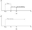
도 1은 본 발명의 제 1 실시예에 따른 차량 조명용 LED 시스템에 포함되는 LED 패키지로서, 도 1(a)는 LED 패키지의 외관이고 도 1(b)는 LED 패키지 내부의 주요 구성을 도시한 도면이다.
도 2는 본 발명의 제 1 실시예에 따른 차량 조명용 LED 시스템의 주요 구성을 도시한 기능블럭도이다.
도 3은 본 발명의 일 실시예에 적용될 수 있는 전류 미러 회로(M)의 예를 도시한 회로도이다.
도 4는 제 1 실시예를 변형한 변형예에 따른 차량 조명용 LED 시스템을 도시한 블럭도이다.
도 5는 본 발명의 일 실시예에 따른 차량 조명용 LED 시스템의 전기적 특성을 도시한 그래프로서, 도 5(a)는 입력전압에 따른 전류 특성을 도시한 것이고 도 5(b)는 입력전압에 따른 전력 특성을 도시한 것이다.
도 6은 본 발명의 제 2 실시예에 따른 차량 조명용 LED 시스템의 주요 구성을 도시한 도면이다.
도 7은 본 발명의 제 2 실시예에 따른 차량 조명용 LED 시스템의 전기적 특성을 도시한 그래프로서, 도 7(a)는 입력전압에 따른 전류 특성을 도시한 것이고 도 7(b)는 입력전압에 따른 전력 특성을 도시한 것이다.
도 8은 실제 자동차에서 사용 중인 기존 구동 방식과 본 발명의 일 실시예에 따른 방식을 비교 Test한 결과를 도시한 그래프이다.1 is an LED package included in an LED system for vehicle lighting according to a first embodiment of the present invention, and FIG. 1(a) is an exterior view of the LED package, and FIG. 1(b) is a view showing a main configuration inside the LED package. to be.
2 is a functional block diagram showing the main configuration of the LED system for vehicle lighting according to the first embodiment of the present invention.
3 is a circuit diagram showing an example of a current mirror circuit M applicable to an embodiment of the present invention.
4 is a block diagram showing a vehicle lighting LED system according to a modified example of the first embodiment.
Figure 5 is a graph showing the electrical characteristics of the LED system for vehicle lighting according to an embodiment of the present invention, Figure 5 (a) shows the current characteristics according to the input voltage, Figure 5 (b) is It shows the power characteristics.
6 is a view showing the main configuration of the LED system for vehicle lighting according to the second embodiment of the present invention.
7 is a graph showing the electrical characteristics of the LED system for vehicle lighting according to the second embodiment of the present invention. FIG. 7(a) shows the current characteristics according to the input voltage, and FIG. 7(b) is It shows the power characteristics according to.
8 is a graph showing a result of a comparison test between a conventional driving method used in an actual vehicle and a method according to an embodiment of the present invention.
첨부한 도면을 참고로 하여 본 발명의 실시예에 대하여 본 발명이 속하는 기술 분야에서 통상의 지식을 가진 자가 용이하게 실시할 수 있도록 상세히 설명한다. 그러나 본 발명은 여러 가지 상이한 형태로 구현될 수 있으며 여기에서 설명하는 실시예에 한정되지 않는다. 그리고 도면에서 본 발명을 명확하게 설명하기 위해서 설명과 관계없는 부분은 생략하였으며, 명세서 전체를 통하여 유사한 부분에 대해서는 유사한 명칭 및 도면 부호를 사용한다.Embodiments of the present invention will be described in detail with reference to the accompanying drawings so that those of ordinary skill in the art may easily implement the present invention. However, the present invention may be implemented in various different forms and is not limited to the embodiments described herein. In the drawings, parts irrelevant to the description are omitted in order to clearly describe the present invention, and similar names and reference numerals are used for similar parts throughout the specification.
도 1은 본 발명의 제 1 실시예에 따른 차량 조명용 LED 시스템에 포함되는 LED 패키지로서, 도 1(a)는 LED 패키지의 외관이고 도 1(b)는 LED 패키지 내부의 주요 구성을 도시한 도면이다.1 is an LED package included in an LED system for vehicle lighting according to a first embodiment of the present invention, and FIG. 1(a) is an exterior view of the LED package, and FIG. 1(b) is a view showing a main configuration inside the LED package. to be.
도 2는 본 발명의 제 1 실시예에 따른 차량 조명용 LED 시스템의 주요 구성을 도시한 기능블럭도이다.2 is a functional block diagram showing the main configuration of the LED system for vehicle lighting according to the first embodiment of the present invention.
본 발명의 제 1 실시예에 따른 차량 조명용 LED 시스템은 크게 LED 패키지(10), 외부 트랜지스터(20), 전류 센싱 저항(30) 및 전류 셋 저항(40)을 포함하여 구성된다. 그리고 LED 패키지(10)는 서로 직렬 연결된 제 1 LED 칩(11)(이하 'LED1'이라고도 한다) 및 제 2 LED 칩(12)(이하 'LED2'라고도 한다)과 구동회로(13)를 포함하여 구성되는 데, 본 발명의 실시예는 LED 칩과 구동회로가 단일의 패키지에 함께 구성되는 형태이다. 제 1 LED 칩(11)의 Anode는 LED 패키지의 Anode 단자를 통하여 입력전압(Vin)을 공급받으며, 제 1 LED 칩(11)의 Cathode는 제 2 LED 칩(12)의 Anode와 연결되고 제 2 LED 칩(12)의 Cathode는 LED 패키지의 Cathode 단자를 통하여 외부 트랜지스터(20)과 연결된다.The LED system for vehicle lighting according to the first embodiment of the present invention largely includes an
기본적인 시스템 형태는 최소한 LED chip 2EA와 고효율/고신뢰성을 위한 구동회로(13)가 포함되는 LED 패키지와, 종래 방식에서 열분배저항의 역할을 하는 외부 트랜지스터(20)를 포함한다.The basic system type includes an LED package including at least 2 LED chips and a driving
외부 트랜지스터(20)는 FET(Field Effect Transistor), 바이폴라 트랜지스터, IGBT(Insulated Gate Bipolar mode Bransistor) 등이 가능하며, 대표적으로는 FET가 선호된다. 외부 트랜지스터(20)는 LED 패키지(10)의 외부에서 LED 패키지(10)의 단자(Cathode)를 통하여 제 1 LED 칩(11) 및 제 2 LED 칩(12)과 연결된다. 외부 트랜지스터(20)는 일단이 제 2 LED 칩(12)의 Cathode와 연결되며 타단은 전류 센싱 저항(3)과 연결되어 외부 트랜지스터의 주된 전류 채널(이하 '주전류 채널'이라고도 하며, FET인 경우 드레인-소스 경로를 말한다)이 제 1 LED 칩(11) 및 제 2 LED 칩(12)과 직렬 연결되며, 게이트는 구동회로(13)에 연결되어 구동회로(13)의 제어신호를 수신한다.The
구동회로(13)는 제 1 LED 칩(11) 및 제 2 LED 칩(12)의 구동과 외부 트랜지스터(20)의 동작을 제어하기 위한 것으로서, 구동회로(13)는 직렬 연결된 제 1 LED 칩(11) 및 제 2 LED 칩(12) 중에서, 입력전압의 크기가 기준전압 보다 작을 때에는 제 1 정전류로 제 1 LED 칩(11)만을 구동하며, 입력전압의 크기가 기준전압 보다 클 때에는 제 2 정전류로 제 1 LED 칩(11) 및 제 2 LED 칩(12) 등을 구동한다. 구동회로(13)는 제 1 LED 칩(11)만이 구동될 때 제 1 LED 칩(11)에서의 파워와, 직렬연결된 제 1 LED 칩(11) 및 제 2 LED 칩(12) 등이 모두 구동될 때 제 1 LED 칩(11) 및 상기 제 2 LED 칩(12)에서의 파워가 동일하게 되도록 제 1 정전류 및 상기 제 2 정전류를 제어한다.The driving
고효율/고신뢰성을 위한 구동회로(13)의 역할은 LED chip 2EA의 구동 형태가 변화하더라도(예를 들어, LED1만 구동 혹은 LED1 + LED2 + FET 동시구동) LED 칩 전체의 Power를 일정하게 유지한다. 입력전압의 변화가 있더라고 LED 전체 Power가 동일하게 되도록 LED chip의 구동을 변화시키며, 높은 입력전압에서도 LED의 발열을 낮추기위해 종래 열분배저항의 역할을 하는 외부 트랜지스터(20)를 컨트롤한다. 추가적으로 Protection 기능 및 구동회로 온도감지를 통하여 LED1과 LED1+LED2+FET 구동을 변경하는 기능 또한 내장되어 있다.The role of the driving
전류 센싱 저항(30)은 일단이 외부 트랜지스터(20)의 주전류 채널과 직렬 연결되고 타단은 접지에 연결되어, LED1, LED2 및 외부 트랜지스터를 통한 경로의 전류를 센싱하기 위한 역할을 수행하는 데, 구체적으로 전류 센싱 저항에 흐르는 전류와 저항을 곱한 전압 신호를 LED 패키지의 단자(CS)를 통하여 구동회로(13)의 비교기(134)로 제공한다.The
전류 셋 저항(40)은 LED 패키지(10)의 외부에서 LED 패키지(10)의 단자(RS)를 통하여 구동회로(13)에 연결되는 데, 구동회로의 일부분과 함께 전류미러 회로(M)를 구성하며, 제 1 정전류를 세팅(설정)하는 데 사용된다.The
구동회로(13)는, 구동회로의 각 부분에 전원을 공급하는 전원 생성 회로(133); 제 1 LED 칩(11) 및 제 2 LED 칩(12)이 연결된 노드에 드레인이 연결되고 접지에 소스가 연결되는 제 1 FET(132); 전류 미러 회로(M)(구체적으로, 미러용 회로(136))에 대하여 제 1 제어 전압을 제공하는 제 1 기준값 생성회로(138); 비교기(134)에 대하여 제 2 제어 전압을 제공하는 제 2 기준값 생성회로(135); 제 2 기준값 생성 회로(135)로부터의 제 2 제어 전압과 전류 센싱 저항(30)으로부터의 전압을 비교한 결과를 출력하는 비교기(134); 프로텍션 상황시에는 외부 트랜지스터(20)를 OFF 시키는 전압을 외부 트랜지스터(20)의 게이트로 인가하고 평상시에는 비교기(134)의 출력에 따라 외부 트랜지스터(20)의 게이트 전압을 컨트롤하는 외부 트랜지스터 구동 게이트 드라이버(137); LED 패키지(10)의 온도를 센싱하는 온도 센서(139); 전류 셋 저항(40)을 더 이용하여 전류 미러 회로(M)을 구성하는 미러용 회로(136); 구동회로의 각 부분으로부터 전압이나 센싱신호를 입력받아 구동회로의 각 부분을 제어하는 제어부(131) 등을 포함하여 구성된다.The driving
제어부(131)는 입력전압(Vin), LED1의 전압(구체적으로 LED1의 Cathode 전압)(VLED1), LED2의 전압(구체적으로 LED2의 Cathode 전압)(VLED2) 및 외부 트랜지스터의 게이트 전압(VGATE)과 온도 센서의 센싱결과 신호 등을 입력받고 구동회로의 각 부분을 제어하는 데, 제 1 기준값 생성회로(138)에 대하여 설정될 제 1 비교전압의 정보를 제공하고 제 2 기준값 생성회로(135)에 대하여 설정될 제 2 비교전압의 정보를 제공하며, 외부 트랜지스터 구동 게이트 드라이버(137)에 대하여 프로텍션 상황에 대한 제어신호를 제공하며, 이들에 필요한 연산과 제어를 수행한다.The
구동회로(13)는 입력전압의 크기가 기준전압 보다 작을 때에는 제 1 FET(132)를 통하여 제 1 정전류가 흐르도록 제 1 FET(132)의 게이트를 제어하며, 제 2 LED 칩(12)와 외부 트랜지스터(20)를 통한 경로로는 전류가 흐르지 않도록 외부 트랜지스터(20)의 게이트를 제어한다. 또한, 구동회로(13)는 입력전압의 크기가 기준전압 보다 클 때에는 제 1 FET(132)가 OFF 되도록 제 1 FET(132)의 게이트를 제어하고 제 2 정전류가 제 1 LED 칩, 제 2 LED 칩 및 외부 트랜지스터를 통하여 흐르도록 외부 트랜지스터(20)의 게이트 전압을 컨트롤한다.The driving
구동회로(13)는 LED 패키지(10)의 단자(CS)를 통하여 전류 센싱 저항(30)에 걸리는 전압를 입력받으며, 전류 센싱 저항(30)에 걸리는 전압과 구동회로가 제 2 정전류의 결정에 따라 설정되는 전압을 비교한 결과로써 외부 트랜지스터(20)의 게이트를 제어함으로써 외부 트랜지스터를 통하여 제 2 정전류가 흐로도록 한다.The driving
낮은 입력 전압(예를 들면 기준전압 이하)에서는 LED 패키지의 RS 단자(pin)의 외부 저항(전류 셋 저항)을 통하여 LED1의 기본 정전류 설정 값을 설정하여 LED1을 정전류 구동을 한다. 입력전압이 높아져서 LED1과 LED2의 직렬 구동이 가능한 높은 전압 영역(기준전압 이상)이 되면, LED 패키지의 CS 단자(pin)의 외부 저항(전류 센싱 저항)을 통하여 LED1 + LED2 + 외부 트랜지스터를 정전류 구동하게 만든다.At low input voltage (eg, below the reference voltage), LED1 is driven at constant current by setting the basic constant current setting value of LED1 through an external resistance (current set resistance) of the RS terminal (pin) of the LED package. When the input voltage becomes high and becomes a high voltage area (above the reference voltage) in which LED1 and LED2 can be driven in series, LED1 + LED2 + external transistors are driven at constant current through the external resistance (current sensing resistance) of the CS terminal (pin) of the LED package. Make it.
이때 높은 전압 영역에서는 LED1 + LED2의 구동 Power 이외의 Power는 외부 트랜지스터에 인가되게 만들어 넓은 구동 범위와 발열 안정성을 확보 할 수 있다. 특히 외부 트랜지스터는 LED 패키지의 외부에 있으므로 외부 트랜지스터의 발열은 LED 패키지에 영향을 미치지 않는다. 이에 따라 LED 패키지의 내부에 구성되는 LED1, LED2 및 구동회로에 영향을 미치지 않아 LED 패키지(구동회로)의 동작 신뢰성을 확보하며, 높은 전압 영역에서 외부 트랜지스터로 하여금 큰 파워 소모를 담당하게 할 수 있으므로 LED 패키기의 구동회로가 큰 파워 소모를 분담하게 하는 것과 비교하여 LED 패키지를 보다 작게 구현할 수 있다. 그리고, 낮은 전압 영역에서는 외부 트랜지스터를 거치지 않는 경로(또한 LED2 도 거치지 않는 경로)로 구동 전류가 흐르게 하므로 종래에 비하여 보다 낮은 입력 전압(예를 들면 7V 보다 낮은 5V까지의 영역)에서도 구동이 가능하게 된다.At this time, in the high voltage region, power other than the driving power of LED1 + LED2 is applied to an external transistor, so that a wide driving range and heat generation stability can be secured. In particular, since the external transistor is outside the LED package, heat generated by the external transistor does not affect the LED package. Accordingly, the operation reliability of the LED package (driving circuit) is secured by not affecting the LED1, LED2 and the driving circuit configured inside the LED package, and the external transistor can be in charge of large power consumption in the high voltage region. Compared to that the driving circuit of the LED package shares large power consumption, the LED package can be implemented smaller. And, in the low voltage region, the driving current flows through a path that does not go through an external transistor (also a path that does not go through LED2), so it is possible to drive even in a lower input voltage (for example, a region of up to 5V lower than 7V) compared to the prior art. do.
전류 미러 회로(M)는 전류 셋 저항(40)과 미러용 회로(136)을 포함하여 제 1 FET(132)의 게이트와 연결되는 전류 미러 회로(M)를 구성한다. 전류 미러 회로(M)는 구동회로(13)의 제어부(131)에 의하여 제어 전압을 입력받되, 구체적으로 보면 제어부(131)는 제 1 기준값 생성회로(138)가 상기 제어 전압을 출력할 수 있도록 제어 전압 정보를 제 1 기준값 생성회로(138)에 대하여 제공할 수 있다. 그리고 전류 미러 회로(M)는 전류 셋 저항(40)에 흐르는 전류의 미러 전류가 제 1 FET(132)를 통하여 흐르도록 제 1 FET(132)의 게이트 전압을 제어한다.The current mirror circuit M comprises a
도 3은 본 발명의 일 실시예에 적용될 수 있는 전류 미러 회로(M)의 예를 도시한 회로도이다.3 is a circuit diagram showing an example of a current mirror circuit M applicable to an embodiment of the present invention.
도 3의 예에서 도시된 전류 미러 회로(M)는 공지된 기술이므로 구체적인 설명을 생략한다. 다만, 전류 미러 회로(M)에 입력되는 제어 전압(VREF)('제 1 제어 전압')과 전류 셋 저항(RS)의 값에 따라 전류 셋 저항(RS)에 흐르는 1차 전류가 결정되며, 1차 전류에 대하여 고정된 비율을 가진 2차 전류(IOUT)(상기한 '제 1 정전류'가 된다)가 제 1 FET(132)의 드레인-소스 경로로 흐르게 한다.Since the current mirror circuit M shown in the example of FIG. 3 is a known technique, a detailed description thereof will be omitted. However, the primary current flowing through the current set resistor RS is determined according to the value of the control voltage VREF ('first control voltage') and the current set resistance RS input to the current mirror circuit M. , A secondary current IOUT (which becomes the above-described'first constant current') having a fixed ratio with respect to the primary current flows through the drain-source path of the
한편, 입력 전압이 높은 전압 영역에 도달하면, 제어부의 제어(제어 정보)에 의해서 제 2 기준값 생성회로(135)는 제 2 제어 전압을 비교기(143)의 +입력으로 제공하며, 전류가 전류 센싱 저항(30)에 흐르면서 전류 센싱 저항(30)에 걸리는 전압은 비교기(134)의 -입력이 되며, 비교기(143)는 이들을 비교한 결과를 출력한다. 비교기(143)의 출력에 따라 외부 트랜지스터 구동 게이트 드라이버(137)는 외부 트랜지스터(20)의 게이트 전압을 올리거나 내리게 되며, 이에 따라 외부 트랜지스터(20)에 흐르는 전류를 증가시키거나 낮추는 동작을 하게 되며, 이러한 전류의 증감과 그에 따른 전류 센싱 저항에 걸리는 전압의 변동은 다시 비교기의 입력에 반영됨으로써 피드백 루프를 구성하게 된다. 이러한 피드백 작용에 따라 전류 센싱 저항에 걸리는 전압은 제 2 제어 전압으로 수렴하게 되며, 결국 전류 센싱 저항이 결정된 상태에서 제 2 구동 전류는 제 2 제어 전압에 의해 결정된다.On the other hand, when the input voltage reaches the high voltage region, the second reference
본 발명의 일 실시예에 따르면, 높은 전압 영역의 구동에서는 저항(즉, 전류 센싱 저항)을 통과하는 경로로 전류(제 2 정전류)가 흐르지만, 낮은 전압 영역의 구동에서는 저항(즉, 전류 셋 저항)을 통과하지 않는 경로로 전류(제 1 정전류)가 흐르도록 한다.According to an embodiment of the present invention, in driving in a high voltage region, a current (second constant current) flows through a path through a resistance (ie, a current sensing resistor), but in driving in a low voltage region, a resistance (ie, a current set) flows. A current (first constant current) flows through a path that does not pass through resistance).
높은 전압 영역의 구동에서는 전류 센싱 저항이 약간의 열분배 저항 역할과 전압 분배 효과를 가지도록 하는 반면, 낮은 전압 영역에서는 전류 경로에 저항을 없애서 보다 낮은 전압에서도 LED(LED1)의 구동이 가능하도록 하는 효과를 가진다.In the driving of the high voltage region, the current sensing resistor acts as a heat divider and has a voltage divider effect, whereas in the low voltage region, the LED (LED1) can be driven at a lower voltage by removing the resistance in the current path. Has an effect.
본 발명의 또다른 특징은 LED 패키지의 온도에 따라 기준전압을 가변하는 점이다. 구동회로(13)는 온도 센서(139)가 센싱한 온도값에 따라 기준전압을 변동시키되, 온도값이 올라갈수록 상기한 기준전압을 낮춘다. 본 발명에서는 입력 전압에 있어서 낮은 전압 영역과 높은 전압 영역을 가르는 기준 전압을 온도 센서의 입력을 이용하여 가변시키는 데, 예를 들어 보통의 온도 범위에서는 기준전압이 9V가 되도록 하지만, LED 패키지의 온도가 일정 온도이상으로 높아지면 기준전압을 8V로 낮추는 것과 같이 동작한다. 이에 따라 더 낮은 기준전압에서 LED1 + LED2 + 외부FET 구동이 시작되도록 한다.Another feature of the present invention is that the reference voltage is varied according to the temperature of the LED package. The driving
본 발명의 일 실시예에 따라 동일 전력이 되도록 제어 방법에서는 LED PKG 내 LED1/LED2의 전기적 특성에 맞게 각 제어전압이 고정값을 갖도록하고 RS/CS 저항을 설정하여 P1=P2가 동일하도록 할 수 있다. 다른 제어 방법에서는, 내부 구동회로에 의해 자동으로 P1=P2가 되도록 구현하는 방법으로서, 한쪽의 정전류가 결정되면 자동으로 다른 쪽의 정전류가 결정되도록 계산되며, 이때 센싱되는 전압들값들이 이용될 수 있다. 예를 들어 제 1 제어 전압은 제 2 제어 전압과 제어부로 입력되는 전압값들로부터 계산될 수 있다.In a control method to have the same power according to an embodiment of the present invention, each control voltage can have a fixed value according to the electrical characteristics of LED1/LED2 in the LED PKG and set the RS/CS resistance so that P1=P2 is the same. have. In another control method, P1 = P2 is automatically implemented by the internal driving circuit. When one constant current is determined, the other constant current is automatically determined, and the sensed voltage values can be used. have. For example, the first control voltage may be calculated from the second control voltage and voltage values input to the controller.
도 4는 제 1 실시예를 변형한 변형예에 따른 차량 조명용 LED 시스템을 도시한 블럭도이다.4 is a block diagram showing a vehicle lighting LED system according to a modified example of the first embodiment.
변형예에서는 전류 셋 저항이 없어지고 EN/PWM 기능이 추가된 형태로 구성된다. 낮은 입력 전압 영역에서 제 1 실시예는 LED 패키지의 RS 단자에 연결되는 외부 저항을 이용하여 LED1의 기본 정전류(제 1 정전류)를 설정하였으나, 변형예에서는 내부 퓨징을 통하여 설정하도록 변형되었다(미도시). 예를 들면, 복수의 저항을 직·병렬로 구성하거나 저항 네트워크를 구성한 다음 퓨징을 통하여 제 1 실시예에 개시된 전류 셋 저항의 역할을 하는 실효 저항을 설정한 후 이용하는 방식이다.In the modified example, the current set resistance is removed and the EN/PWM function is added. In the low input voltage region, the first embodiment sets the basic constant current (first constant current) of LED1 using an external resistor connected to the RS terminal of the LED package, but in the modified example, it has been modified to be set through internal fusing (not shown). ). For example, a plurality of resistors are configured in series or parallel, or a resistance network is formed, and then an effective resistance serving as a current set resistor disclosed in the first embodiment is set through fusing and then used.
한편, 변형예에서는 외부 EN/PWM신호 입력시 LED1 구동 혹은 LED1 + LED2 구동할때 On/Off 구동 및 PWM 구동을 하는 것이 제 1 실시예와 다르다. 이때도 전 입력 전압 영역에서 EN/PWM신호에 맞는 LED 전체 Power는 일정하며, 고효율 및 고신뢰성 구동을 하는 것은 동일하다.On the other hand, in the modified example, on/off driving and PWM driving when driving LED1 or LED1 + LED2 when external EN/PWM signals are input are different from the first embodiment. Even at this time, the total power of the LED that fits the EN/PWM signal in the entire input voltage range is constant, and the high-efficiency and high-reliability driving is the same.
도 5는 본 발명의 일 실시예에 따른 차량 조명용 LED 시스템의 전기적 특성을 도시한 그래프로서, 도 5(a)는 입력전압에 따른 전류 특성을 도시한 것이고 도 5(b)는 입력전압에 따른 전력 특성을 도시한 것이다.Figure 5 is a graph showing the electrical characteristics of the LED system for vehicle lighting according to an embodiment of the present invention, Figure 5 (a) shows the current characteristics according to the input voltage, Figure 5 (b) is It shows the power characteristics.
도 5 에 되시된 것과 같이 입력전압이 LED1 구동전압 영역(VLED1 ~ V1)에서는 LED1만 구동하게 만들고 더 높은 전압이 인가되어 LED2 까지 구동가능한 영역(V1 ~ )에서는 직렬의 LED1 및 LED2와 연결된 외부 트랜지스터에 의하여 정전류 구동을 한다. 이때 LED1 / LED2의 전압 감지 및 정전류 설정 값을 변경함으로써 입력전압이 가변되더라도, 도 5(b)에 도시된 바와 같이 LED 전체의 Power[P(LED Total Power)]는 일정하게 만들어 동일 광량을 유지한다.As shown in Fig. 5, the input voltage drives LED1 only in the LED1 driving voltage region (VLED1 ~ V1 ), and a higher voltage is applied to the driving range (V1 ~) to LED2 in series with LED1 and LED2. Constant current driving is performed by the connected external transistor. At this time, even if the input voltage is changed by detecting the voltage of LED1 / LED2 and changing the constant current setting value, the power [P(LED Total Power) ] of the entireLED is made constant as shown in Fig. 5(b) to maintain the same amount of light. do.
LED1만 구동이 되는 영역에서는 내부의 구동 회로를 통하는 경로로 흐르는 정전류(ILED1)에 의해서 LED 전체 Power를 일정하게 하고 그 이외의 높은 전압 영역, 즉 LED2 까지 구동가능한 영역에서는 외부 트랜지스터를 통하는 경로로 흐르는 정전류(ILED1+LED2+FET)에 의해서 LED 전체 Power를 일정하게 만들어서 고전압 입력 영역에서 구동회로의 발열 문제를 해결 할 수 있다.In the area where only LED1 is driven, the entire power of the LED is made constant by the constant current (ILED1 ) flowing through the path through the internal driving circuit, and in the other high voltage area, that is, the area capable of driving up to LED2, the path through an external transistor is used. By making the entire power of the LED constant by flowing constant current (ILED1+LED2+FET ), it is possible to solve the heat generation problem of the driving circuit in the high voltage input area.
외부 트랜지스터 구동을 통하여 종래 방식에 따른 열분배 저항의 문제점인 구동영역 제한을 해결 할 수 있다. 이에 따라 LED1+LED2의 구동 전압을 최대 효율이 가능한 LED Vf 값으로 설정할 수 있게 하며, 고효율 및 발열 문제를 해결한 고신뢰성 시스템 구현이 가능하게 된다.By driving the external transistor, it is possible to solve the limitation of the driving region, which is a problem of the heat distribution resistance according to the conventional method. Accordingly, it is possible to set the driving voltage of LED1+LED2 to the LED Vf value that can achieve maximum efficiency, and it is possible to implement a highly reliable system that solves the problem of high efficiency and heat generation.
도 6은 본 발명의 제 2 실시예에 따른 차량 조명용 LED 시스템의 주요 구성을 도시한 도면이다.6 is a view showing the main configuration of the LED system for vehicle lighting according to the second embodiment of the present invention.
이하에서는 제 1 실시예와 비교하여 서로 다른 점을 중심으로 설명하며 동일 또는 유사한 내용에 대해서는 생략될 수 있다.Hereinafter, the description will focus on different points compared to the first embodiment, and the same or similar contents may be omitted.
LED 시스템은 LED 패키지(10)와 그 외부에 구성되는 열분배 저항(50) 등을 포함하여 구성된다.The LED system includes an
LED 패키지(10)는 서로 직렬 연결된 제 1 LED 칩(11) 및 제 2 LED 칩(12)과, 제 1 LED 칩(11) 및 제 2 LED 칩(12)의 구동을 제어하기 위한 구동회로(13)를 포함하여 구성되며, 열분배 저항(50)은 LED 패키지(10)의 외부에서 LED 패키지(10)의 단자(Cathode)를 통하여 제 1 LED 칩(11) 및 제 2 LED 칩(12)과 일단이 직렬 연결되고 타단은 LED 패키지(10)의 단자(DR)에 연결된다. 즉, 열분배 전항의 양단은 LED 패키지에 모두 연결된다.The
구동회로(13)는, 입력전압의 크기가 제 1 기준전압 보다 작을 때(제 1 전압 범위)에는 제 1 LED 칩(11)과 제 1 FET(141)를 지나 접지로 가는 경로로 제 1 정전류가 흐르도록 구동하며, 입력전압의 크기가 제 1 기준전압 보다 크고 제 2 기준전압 보다 작을 때(제 2 전압 범위)에는 직렬 연결된 제 1 LED 칩(11) 및 제 2 LED 칩(12)과 제 2 FET(142)를 지나 접지로 가는 경로로 제 2 정전류가 흐르도록 구동하며, 입력전압의 크기가 제 2 기준전압 보다 클 때(제 3 전압 범위)에는 직렬 연결된 제 1 LED 칩(11) 및 제 2 LED 칩(12)와 열분배 저항(50)을 통하고 제 3 FET(143)를 지나는 경로로 동일한 제 2 정전류(제 2 전압 범위일 때의 전류와 동일함)가 흐르도록 구동한다.When the magnitude of the input voltage is smaller than the first reference voltage (the first voltage range), the driving
구동회로(13)는, 제 1 LED 칩(11)만이 구동될 때(입력전압이 제 1 전압 범위일때) 제 1 LED 칩(11)의 파워와, 직렬 연결된 제 1 LED 칩(11) 및 제 2 LED 칩(12)를 지나 접지로 가는 경로로 구동될 때(입력전압이 제 2 전압 범위일때) 제 1 LED 칩(11) 및 제 2 LED 칩(12)의 파워와, 직렬 연결된 제 1 LED 칩(11) 및 제 2 LED 칩(12)와 열분배 저항(50)을 통한 경로로 구동될 때(입력전압이 제 3 전압 범위일때) 제 1 LED 칩(11) 및 제 2 LED 칩(12)의 파워는 동일하게 되도록 제어한다.The driving
구동회로(13)는 제 1 FET(141), 제 2 FET(142) 및 제 3 FET(143)을 포함하며, 그리고 구동회로(13)는, 구동회로의 각 부분에 전원을 공급하는 전원 생성 회로(133)와, LED 패키지(10)의 온도를 센싱하는 온도 센서(139)와, 구동회로의 각 부분으로부터 전압이나 센싱신호를 입력받아 구동회로의 각 부분을 제어하는 제어부(131) 등을 포함하여 구성된다.The driving
제 1 FET(141)는 제 1 LED 칩(11)과 제 2 LED 칩(12)이 연결된 노드에 드레인이 연결되고 접지에 소스가 연결되고 제 1 전류 미러 회로(M1)에 의해 게이트 전압이 컨트롤된다. 제 2 FET(142)는 제 2 LED 칩(12)과 열분배 저항(50)이 연결된 노드에 드레인이 연결되고 접지에 소스가 연결되며 제 2 전류 미러 회로(M2)에 의해 게이트 전압이 컨트롤된다. 제 3 FET(143)는 열분배 저항(50)의 타단이 드레인에 연결되고 접지에 소스가 연결되며 제 2 전류 미러 회로(M2)에 의해 게이트 전압이 컨트롤된다.In the
구동회로(13)는, 입력전압의 크기가 제 1 기준전압 보다 작을 때(제 1 전압 범위)에는 제 2 FET(142) 및 제 3 FET(143)를 OFF 하도록 하고 제 1 FET(141)을 통하여 제 1 정전류가 흐르도록 제어하며, 입력전압의 크기가 제 1 기준전압 보다 크고 제 2 기준전압 보다 작을 때(제 2 전압 범위)에는 제 1 FET(141) 및 제 3 FET(143)를 OFF 하도록 하고 제 2 FET(142)를 통하여 제 2 정전류가 흐르도록 제어하고, 입력전압의 크기가 제 2 기준전압 보다 클 때(제 3 전압 범위)에는 제 1 FET(141) 및 제 2 FET(142)를 OFF 하도록 하고 제 3 FET(143)을 통하여 제 2 정전류가 흐르도록 제어한다.The driving
제 1 전류 셋 저항(41)은 LED 패키지(10)의 외부에서 LED 패키지(10)의 단자(RS1)를 통하여 구동회로(13)에 연결되며, 구동회로(13)에 대하여 제 1 정전류를 세팅한다. 제 2 전류 셋 저항(42)은 LED 패키지(10)의 외부에서 LED 패키지의 단자(RS2)를 통하여 구동회로(13)에 연결되며, 구동회로(13)에 대하여 제 2 정전류를 세팅한다.The first
제 1 전류 셋 저항(41)을 포함하여 제 1 FET(141)의 게이트와 연결되는 제 1 전류 미러 회로(M1)를 구성하는 데, 예를 들면 도 3에 도시된 전류 미러 회로(M)와 동일하게 구성된다. 제 1 전류 미러 회로(M1)는 구동회로(13)의 제어부(131)에 의하여 제 1 제어 전압을 입력받는 데, 예를 들면 제어부(131)는 제 1 제어 전압 정보를 제 1 기준값 생성회로(136)에 제공하며 제 1 기준값 생성회로(136)는 제 1 제어 전압을 출력한다. 그리고 제 1 미러 회로는 제 1 전류 셋 저항(41)에 흐르는 전류의 미러 전류가 제 1 FET(141)를 통하여 흐르도록 제 1 FET(141)의 게이트 전압(VC1)을 제어한다.A first current mirror circuit M1 including a first
제 2 전류 셋 저항(42)을 포함하여 제 2 FET(142)의 게이트 및 제 3 FET(143)의 게이트와 연결되는 제 2 전류 미러 회로(M2)를 구성한다. 제 2 전류 미러 회로(M2)는, 구동회로(13)의 제어부(131)에 의하여 제어 전압을 입력받는 데, 예를 들면 제어부(131)는 제 2 제어 전압 정보를 제 2 기준값 생성회로(144)에 제공하며 제 2 기준값 생성회로(144)는 제 2 제어 전압을 출력한다. 그리고 제 2 미러 회로는 제 2 전류 셋 저항(42)에 흐르는 전류의 미러 전류가 제 2 FET(142) 또는 제 3 FET(142)를 통하여 흐르도록 제 2 FET(142) 및 제 3 FET(143)의 게이트 전압을 각각 제어하되, 전압 범위에 따라 제 2 FET(142) 또는 제 3 FET(143)가 동작되도록 한다. 이러한 형태의 전류 미러 회로는 예를 들어 도 3에 도시된 전류 미러 회로에서 오른쪽 부분의 회로 또는 제 2 FET(142) 및 제 3 FET(143)의 게이트가 2개 병렬로 연결된 것일 수 있다. 한편, 제 2 FET(142) 또는 제 3 FET(143)를 선택적으로 동작시키기 위하여 두 병렬 접속 경로에 스위칭 트랜지스터를 구성하고 제어부의 제어에 따라 선택하도록 할 수 있다.A second current mirror circuit M2 connected to the gate of the
온도 센서(139)는 LED 패키지(10)의 내부에 구성되어 LED 패키지(10)의 온도를 센싱한다. 구동회로(13)는 온도 센서(139)가 센싱한 온도값에 따라 상기한 1 기준전압 및 제 2 기준전압을 변동시키되, 온도값이 올라갈수록 제 1 기준전압 및 제 2 기준전압을 낮춘다.The
열분배저항을 사용한 제 2 실시예에서 구동회로는 LED chip 2EA 구동의 형태가 변화하더라도(예를 들어, LED1만 구동, LED1+LED2 동시구동, LED1+LED2+열분배저항 동시구동), LED 전체의 Power를 일정하게 유지한다. 또한 입력전압의 변화에 따라 LED 전체 Power(동일 광량)가 동일하도록 LED chip의 구동을 변화시키며, 높은 입력 전압에서도 LED의 발열을 낮추기 위해 외부 열분배저항을 이용해 구동이 되도록 컨트롤 한다. 이에 따라 높은 입력전압에서 외부의 열분배 저항이 발열되므로 LED 패키지의 온도 상승이 저감된다.In the second embodiment using the heat distribution resistor, even if the driving type of the LED chip 2EA changes (e.g., LED1 only, LED1+LED2 simultaneous drive, LED1+LED2+heat distribution resistor simultaneous drive), the entire LED Keep the power constant. Also, according to the change of the input voltage, the driving of the LED chip is changed so that the total power (same amount of light) of the LED is the same, and the driving is controlled using an external heat distribution resistor to reduce the heat generation of the LED even at a high input voltage. Accordingly, since the external heat distribution resistor is heated at a high input voltage, the temperature rise of the LED package is reduced.
낮은 입력 전압 범위에서는 LED 패키지의 RS1 단자(pin)의 외부 저항을 통하여 LED1의 기본 정전류 설정 값을 설정하며 LED1을 정전류(제 1 정전류) 구동을 한다. 입력전압이 높아져서 LED1과 LED2의 직렬 구동이 가능한 전압 범위가 되면, LED 패키기의 RS2 단자(pin)의 외부 저항을 통하여 LED1 + LED2의 기본 정전류 설정 값을 설정하여 LED1 + LED2를 정전류(제 2 정전류)로 직렬 구동을 하게 만든다.In the low input voltage range, the basic constant current setting value of LED1 is set through the external resistance of the RS1 terminal (pin) of the LED package, and the LED1 is driven by a constant current (first constant current). When the input voltage becomes high and the voltage range in which LED1 and LED2 can be driven in series, the default constant current setting value of LED1 + LED2 is set through the external resistance of the RS2 terminal (pin) of the LED package, and LED1 + LED2 is converted to a constant current (the second Constant current) in series drive.
또한 LED 패키지에 높은 발열이 발생하는 보다 더 높은 전압이 인가되면 LED 패키지의 RS2 단자(pin)에 의한 정전류 설정 값(제 2 정전류)을 기준으로 열분배저항까지 포함된 회로, 즉 LED1 + LED2 + 열분배저항을 정전류로 직렬 구동 하게 만든다. 이에 따라 보다 높은 전압 영역에서는 LED1 + LED2의 구동 Power 이외에도 열분배저항의 Power도 소모되게 함으로써, 넓은 구동 범위와 발열 안정성을 확보 할 수 있다.In addition, when a higher voltage is applied to the LED package than generating high heat generation, a circuit that includes a heat distribution resistance based on the constant current setting value (second constant current) by the RS2 terminal (pin) of the LED package, that is, LED1 + LED2 + It makes the heat distribution resistor drive in series with a constant current. Accordingly, in a higher voltage region, power of a heat distribution resistor in addition to the driving power of LED1 + LED2 is consumed, thereby ensuring a wide driving range and heat generation stability.
도 7은 본 발명의 제 2 실시예에 따른 차량 조명용 LED 시스템의 전기적 특성을 도시한 그래프로서, 도 7(a)는 입력전압에 따른 전류 특성을 도시한 것이고 도 7(b)는 입력전압에 따른 전력 특성을 도시한 것이다.7 is a graph showing the electrical characteristics of the LED system for vehicle lighting according to the second embodiment of the present invention. FIG. 7(a) shows the current characteristics according to the input voltage, and FIG. 7(b) is It shows the power characteristics according to.
도 7과 같이 LED1 구동전압 영역에서는 LED1만 구동하게 만들고 더 높은 전압이 인가되어 LED1 + LED2가 구동가능한 영역에서는 LED1 + LED2를 직렬 연결하여 LED1 + LED2를 구동한다. 또한 LED 발열 문제가 발생할 더 높은 전압이 인가되면 외부 열분배저항과 함께 구동한다. 즉 LED1 + LED2 + 열분배저항을 정전류로 직렬 구동한다.As shown in FIG. 7, only LED1 is driven in the LED1 driving voltage area, and a higher voltage is applied to drive LED1 + LED2 by connecting LED1 + LED2 in series in the driving area where LED1 + LED2 can be driven. In addition, when a higher voltage to cause the LED heating problem is applied, it is driven together with an external heat distribution resistor. That is, it drives LED1 + LED2 + heat distribution resistor in series with a constant current.
제어부는 LED1/LED2/열분배저항의 전압 감지 및 정전류 설정 값을 변경함으로써 도 7과 같이 입력전압이 가변되어도 LED 전체 Power는 일정하게 만들어 동일 광량을 유지하는 것이 가장 큰 특징이다. 이때 입력 전압이 올라 갈수록 입력 Power는 올라간다.The most important feature is that the control unit detects the voltage of LED1/LED2/heat distribution resistor and changes the constant current setting value, so that even if the input voltage is varied as shown in FIG. 7, the entire power of the LED is made constant and the same amount of light is maintained. At this time, as the input voltage increases, the input power increases.
본 발명의 제 2 실시에에 따라 열분배저항을 사용한 저가 구동 방식의 시스템 형태는 LED 내부의 LED1만 구동할때나, LED1 + LED2, 혹은 LED1 + LED2 + 열분배저항이 구동되는 영역에서나, 모두 내부 회로를 통하여 LED 전체 Power를 일정하게 만든다. 특히 본 발명의 제 2 실시예에서는 LED1 혹은 LED1+LED2 형태 나아가 LED1 + LED2 + 열분배저항 형태로 선택적으로 구동이 가능함으로써, 낮은 입력 전압에서도 구동이 가능하고 LED1 + LED2 의 구동 전압을 최대 효율이 가능한 LED Vf 값으로 설정할 수 있다. 이를 통하여 종래 방식의 열분배저항의 문제 점인 구동영역 제한을 해결 할 수 있으며, 고효율 특성에 의하여 발열 문제를 해결한 고신뢰성 시스템 구현이 가능하다.According to the second embodiment of the present invention, the system type of the low-cost driving method using the heat distribution resistor is when driving only the LED1 inside the LED, LED1 + LED2, or LED1 + LED2 + the area where the heat distribution resistor is driven. Through the internal circuit, the entire power of the LED is made constant. In particular, in the second embodiment of the present invention, it is possible to drive selectively in the form of LED1 or LED1+LED2 and further in the form of LED1 + LED2 + heat distribution resistor, so that it is possible to drive even at a low input voltage, and the driving voltage of LED1 + LED2 is maximized. It can be set to any possible LED Vf value. Through this, it is possible to solve the limitation of the driving area, which is a problem of the heat distribution resistance of the conventional method, and it is possible to implement a high reliability system that solves the heat generation problem by high efficiency characteristics.
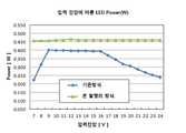
도 8은 실제 자동차에서 사용 중인 기존 구동 방식과 본 발명의 일 실시예에 따른 방식을 비교 Test한 결과를 도시한 그래프이다.8 is a graph showing a result of a comparison test between a conventional driving method used in an actual vehicle and a method according to an embodiment of the present invention.
기존 방식은 낮은 입력 전압(7V ~ 9V)에서 LED Total Power가 낮아 균일한 광량을 나타낼 수 없으며, 높은 입력전압(16V ~ 24V)에서는 시스템의 발열 문제로 LED Total Power를 낮추는 구동 방식을 채택하고 있다. 기존 방식에서는 낮은 입력 전압(7V ~ 9V)에서는 열분배 저항에 걸리는 전압에 의해서 LED에 균일한 광량을 낼수 있는 전압이 인가되지 못하며, 이로 인해 낮은 입력 전압(7V ~ 9V)에서 LED Total Power가 낮아 균일한 광량을 나타낼 수 없다.Existing methods have low LED total power at low input voltages (7V ~ 9V), so they cannot display a uniform amount of light, and at high input voltages (16V ~ 24V), they adopt a driving method that lowers the LED total power due to system heat generation. . In the conventional method, at a low input voltage (7V ~ 9V), the voltage that can emit a uniform amount of light cannot be applied to the LED due to the voltage applied to the heat distribution resistor, and as a result, the LED total power is low at a low input voltage (7V ~ 9V). It cannot show a uniform amount of light.
만약 열분배 저항에 걸리는 전압을 낮추면 아래와 같이 시스템에 걸리는 Power 공식에 의해 구동회로에 걸리는 Power가 높아져서 도 8에 도시된 것과 같이 예를 들면 16V 이상에서는 균일한 광량을 나타낼 수 없다.If the voltage applied to the heat distribution resistor is lowered, the power applied to the driving circuit increases according to the power formula applied to the system as shown below, and as shown in FIG. 8, for example, a uniform amount of light cannot be expressed above 16V.
P(total) = P(열분배저항) + P(total LED) + P(구동회로)P(total) = P(heat distribution resistance) + P(total LED) + P(drive circuit)
높은 입력 전압(16V ~ 24V)에서는 P(열분배저항)과 P(total LED) 값은 일정한 값을 나타내는 상수 값이므로, 전압이 높아질수록 구동회로에 걸리는 Power는 높아 진다. 이로 인해서 기존 구동 방식은 구현하고자 하는 최대의 LED Total power를 낮추던지, 아니면 고전압 영역에서 전압이 높아질수록 기존 구동 방식과 같이 LED Total Power를 낮추는 구동 방식을 채택하고 있다.At high input voltages (16V ~ 24V), the P (heat distribution resistance) and P (total LED) values are constant values representing constant values, so the higher the voltage, the higher the power applied to the driving circuit. For this reason, the existing driving method either lowers the maximum LED total power to be implemented, or adopts a driving method that lowers the LED total power like the existing driving method as the voltage increases in the high voltage region.
따라서 LED 구동과 시스템 발열 안정성 문제로 인하여 낮은 구동영역에서는 정전력 LED구동을 포기하던지 높은 입력전압 영역에서 정전력 LED구동을 포기해야 하는 문제점이 있는 것이다.Therefore, due to the LED driving and system heat stability problems, there is a problem in that constant power LED driving must be abandoned in a low driving region or constant power LED driving in a high input voltage region.
본 발명은 위에 상세하게 설명한 것과 같이 전영역의 전압에서 동일한 Total LED Power를 구현 할 수는 있는 방식이므로 도 8에 도시된 것과 같이 전 시간영역 및 전 입력전압 영역에서 동일한 Total LED Power를 구현한다.In the present invention, as described in detail above, since the same total LED power can be implemented in the entire voltage range, the same total LED power is implemented in the entire time domain and all input voltage areas as shown in FIG. 8.
또한, 본 발명은 높은 효율로 인하여 기존 구동방식의 LED Total Power보다 높은 LED Total Power를 구현 할 수 있음에도 더 작은 IC Package로 구현 할 수 있는 장점이 있다. 또한 핵심 구동 IC 및 주변 부품의 온도도 낮출 수 있어 시스템 신뢰성도 높이는 장점이 있다.In addition, the present invention has the advantage of being able to implement a smaller IC package even though it can implement a higher LED total power than the conventional driving method LED total power due to high efficiency. In addition, the temperature of the core driving IC and peripheral components can be reduced, thereby increasing system reliability.
상기한 본 발명의 설명에서, 제 1 LED 칩 및 제 2 LED 칩의 각각은 편의상 단일의 LED 소자로 도시되어 있으나, 복수의 LED 소자로써 제 1 LED 칩 및/또는 제 2 LED 칩을 구성할 수 있음은 당연하므로 본 발명은 이와 같이 복수의 LED 소자로써 LED 칩을 구성하는 형태를 포함한다. 또한, 상기한 본 발명의 설명에서는 LED 패키지가 2개의 LED 칩을 포함하여 구성되는 것으로 도시되어 있으나, 3개 이상의 LED 칩을 포함하여 구성될 수 있음도 당연하며 이러한 형태도 본 발명의 범주에 포함된다. 예를 들어, 3개의 LED 칩을 포함하는 경우에는 기준전압 및 입력 전압의 범위가 추가로 정의될 수 있다.In the above description of the present invention, each of the first LED chip and the second LED chip is illustrated as a single LED element for convenience, but the first LED chip and/or the second LED chip may be configured as a plurality of LED elements. It is natural that the present invention includes a form of configuring an LED chip with a plurality of LED devices as described above. In addition, in the above description of the present invention, it is shown that the LED package is configured to include two LED chips, but it is natural that it may be configured to include three or more LED chips, and this form is also included in the scope of the present invention. do. For example, in the case of including three LED chips, a range of a reference voltage and an input voltage may be additionally defined.
10 : LED 패키지11, 12 : LED 칩
13 : 구동 회로131 : 제어부
132, 141, 142, 143 : 내부 FET
134 : 비교기135 : 제 2 기준값 생성회로
136 : 미러용 회로137 : 외부 트랜지스터 구동 게이트 드라이버
138 : 제 1 기준값 생성회로20 : 외부 트랜지스터
30 : 전류 센싱 저항40, 41, 42 : 전류 셋 저항10:
13: drive circuit 131: control unit
132, 141, 142, 143: internal FET
134: comparator 135: second reference value generation circuit
136: mirror circuit 137: external transistor driving gate driver
138: first reference value generation circuit 20: external transistor
30: current sensing
Claims (12)
Translated fromKorean상기 LED 패키지(10)의 외부에서 상기 LED 패키지(10)의 단자를 통하여 상기 제 1 LED 칩(11) 및 상기 제 2 LED 칩(12)과 연결되되, 주전류 채널이 직렬 연결되는 외부 트랜지스터(20);를 포함하여 구성되며,
상기 구동회로(13)는,
입력전압의 크기가 기준전압 보다 작을 때에는 제 1 정전류로 상기 제 1 LED 칩(11) 및 상기 제 2 LED 칩(12) 중에서 상기 제 1 LED 칩(11)만을 구동하며, 상기 입력전압의 크기가 상기 기준전압 보다 클 때에는 제 2 정전류로 상기 제 1 LED 칩(11) 및 상기 제 2 LED 칩(12)과 상기 외부 트랜지스터(20)를 구동하되,
상기 제 1 LED 칩(11)만이 구동될 때 상기 제 1 LED 칩(11)에서의 파워와, 상기 직렬연결된 제 1 LED 칩(11) 및 제 2 LED 칩(12)과 상기 외부 트랜지스터(20)의 모두가 구동될 때 상기 상기 제 1 LED 칩(11) 및 상기 제 2 LED 칩(12)에서의 파워가 동일하게 되도록 상기 제 1 정전류 및 상기 제 2 정전류를 제어하며,
상기 제 2 정전류가 상기 제 1 LED 칩, 상기 제 2 LED 칩 및 상기 외부 트랜지스터를 통하여 흐르도록 상기 외부 트랜지스터(20)의 게이트 전압을 컨트롤하는,
것을 특징으로 하는 차량 조명용 LED 시스템.A first LED chip 11 and a second LED chip 12 connected in series with each other, and a driving circuit 13 for controlling driving of the first LED chip 11 and the second LED chip 12; LED package 10 configured to include;
An external transistor connected to the first LED chip 11 and the second LED chip 12 from the outside of the LED package 10 through a terminal of the LED package 10, the main current channel connected in series ( 20); comprises,
The driving circuit 13,
When the level of the input voltage is less than the reference voltage, only the first LED chip 11 of the first LED chip 11 and the second LED chip 12 is driven with a first constant current, and the level of the input voltage is When greater than the reference voltage, the first LED chip 11 and the second LED chip 12 and the external transistor 20 are driven with a second constant current,
When only the first LED chip 11 is driven, the power from the first LED chip 11, the series-connected first LED chip 11 and the second LED chip 12, and the external transistor 20 The first constant current and the second constant current are controlled so that the power in the first LED chip 11 and the second LED chip 12 is the same when all of them are driven,
Controlling the gate voltage of the external transistor 20 so that the second constant current flows through the first LED chip, the second LED chip, and the external transistor,
LED system for vehicle lighting, characterized in that.
상기 외부 트랜지스터(20)의 주전류 채널과 직렬 연결되는 전류 센싱 저항(30);를 더 포함하며,
상기 구동회로는,
상기 LED 패키지(10)의 단자를 통하여 상기 전류 센싱 저항(30)에 걸리는 전압를 입력받으며, 상기 전류 센싱 저항(30)에 걸리는 전압과 상기 구동회로가 상기 제 2 정전류의 결정에 따라 설정되는 전압을 비교한 결과로써 상기 외부 트랜지스터(20)의 게이트를 제어하는,
것을 특징으로 하는 차량 조명용 LED 시스템.The method according to claim 1,
A current sensing resistor 30 connected in series with the main current channel of the external transistor 20; further includes,
The driving circuit,
A voltage applied to the current sensing resistor 30 is input through a terminal of the LED package 10, and a voltage applied to the current sensing resistor 30 and a voltage set by the driving circuit according to the determination of the second constant current As a result of the comparison, controlling the gate of the external transistor 20,
LED system for vehicle lighting, characterized in that.
상기 구동회로(13)는, 제 1 LED 칩(11) 및 제 2 LED 칩(12)가 연결된 노드에 드레인이 연결되고 접지에 소스가 연결되는 제 1 FET(132)를 더 포함하며,
상기 구동회로(13)는,
입력전압의 크기가 기준전압 보다 작을 때에는 상기 제 1 FET(132)를 통하여 상기 제 1 정전류가 흐르도록 상기 제 1 FET(132)의 게이트를 제어하며,
상기 입력전압의 크기가 상기 기준전압 보다 클 때에는 상기 제 1 FET(132)가 OFF 되도록 상기 제 1 FET(132)의 게이트를 제어하는,
것을 특징으로 하는 차량 조명용 LED 시스템.The method according to claim 1,
The driving circuit 13 further includes a first FET 132 having a drain connected to a node to which the first LED chip 11 and the second LED chip 12 are connected and a source connected to the ground,
The driving circuit 13,
When the input voltage is less than the reference voltage, the gate of the first FET 132 is controlled so that the first constant current flows through the first FET 132,
When the level of the input voltage is greater than the reference voltage, controlling the gate of the first FET 132 to turn off the first FET 132,
LED system for vehicle lighting, characterized in that.
상기 LED 패키지(10)의 외부에서 상기 LED 패키지(10)의 단자를 통하여 상기 구동회로(13)에 연결되며 상기 제 1 정전류를 세팅하는 전류 셋 저항(40);를 더 포함하는,
것을 특징으로 하는 차량 조명용 LED 시스템.The method of claim 3,
A current set resistor 40 connected to the driving circuit 13 from the outside of the LED package 10 through a terminal of the LED package 10 and setting the first constant current; further comprising,
LED system for vehicle lighting, characterized in that.
상기 전류 셋 저항(40)을 포함하여 상기 제 1 FET(132)의 게이트와 연결되는 전류 미러 회로(M)를 구성하며,
상기 전류 미러 회로(M)는,
상기 구동회로(13)의 제어부(131)에 의하여 제어 전압을 입력받고 상기 전류 셋 저항(40)에 흐르는 전류의 미러 전류가 상기 제 1 FET(132)를 통하여 흐르도록 상기 제 1 FET(132)의 게이트 전압을 제어하는,
것을 특징으로 하는 차량 조명용 LED 시스템.The method of claim 4,
A current mirror circuit (M) connected to the gate of the first FET (132) including the current set resistor (40),
The current mirror circuit M,
The first FET 132 receives a control voltage by the controller 131 of the driving circuit 13 and the mirror current of the current flowing through the current set resistor 40 flows through the first FET 132. To control the gate voltage of,
LED system for vehicle lighting, characterized in that.
상기 LED 패키지(10)의 내부에 구성되며, 상기 LED 패키지(10)의 온도를 센싱하는 온도 센서(139);를 더 포함하며,
상기 구동회로(13)는,
상기 온도 센서(139)가 센싱한 온도값에 따라 상기 기준전압을 변동시키되, 온도값이 올라갈수록 상기 기준전압을 낮추는,
것을 특징으로 하는 차량 조명용 LED 시스템.The method according to claim 1,
A temperature sensor 139 configured inside the LED package 10 and sensing the temperature of the LED package 10; further includes,
The driving circuit 13,
The reference voltage is changed according to the temperature value sensed by the temperature sensor 139, but lowering the reference voltage as the temperature value increases,
LED system for vehicle lighting, characterized in that.
상기 LED 패키지(10)의 외부에서 상기 LED 패키지(10)의 단자를 통하여 상기 제 1 LED 칩(11) 및 제 2 LED 칩(12)과 일단이 직렬 연결되는 열분배 저항(50);을 포함하여 구성되며,
상기 구동회로(13)는,
입력전압의 크기가 제 1 기준전압 보다 작을 때에는 상기 제 1 LED 칩(11)을 지나 접지로 가는 경로로 제 1 정전류가 흐르도록 구동하며,
상기 입력전압의 크기가 상기 제 1 기준전압 보다 크고 제 2 기준전압 보다 작을 때에는 상기 직렬 연결된 제 1 LED 칩(11) 및 제 2 LED 칩(12)를 지나 접지로 가는 경로로 제 2 정전류가 흐르도록 구동하며,
상기 입력전압의 크기가 상기 제 2 기준전압 보다 클 때에는 상기 직렬 연결된 제 1 LED 칩(11) 및 제 2 LED 칩(12)와 상기 열분배 저항(50)을 통한 경로로 상기 제 2 정전류가 흐르도록 구동하는,
것을 특징으로 하는 차량 조명용 LED 시스템.A first LED chip 11 and a second LED chip 12 connected in series with each other, and a driving circuit 13 for controlling driving of the first LED chip 11 and the second LED chip 12; includes LED package 10 configured by;
A heat distribution resistor 50 having one end connected in series with the first LED chip 11 and the second LED chip 12 through a terminal of the LED package 10 from the outside of the LED package 10 Is composed of
The driving circuit 13,
When the magnitude of the input voltage is less than the first reference voltage, the first constant current is driven to flow through the first LED chip 11 to the ground,
When the magnitude of the input voltage is greater than the first reference voltage and less than the second reference voltage, a second constant current flows through the series-connected first LED chip 11 and the second LED chip 12 to the ground. And
When the magnitude of the input voltage is greater than the second reference voltage, the second constant current flows through a path through the series-connected first LED chip 11 and second LED chip 12 and the heat distribution resistor 50. To drive,
LED system for vehicle lighting, characterized in that.
상기 구동회로(13)는,
상기 제 1 LED 칩(11)만이 구동될 때 상기 제 1 LED 칩(11)의 파워와, 상기 직렬 연결된 제 1 LED 칩(11) 및 제 2 LED 칩(12)를 지나 접지로 가는 경로로 구동될 때 제 1 LED 칩(11) 및 제 2 LED 칩(12)의 파워와, 상기 직렬 연결된 제 1 LED 칩(11) 및 제 2 LED 칩(12)와 상기 열분배 저항(50)을 통한 경로로 구동될 때 제 1 LED 칩(11) 및 제 2 LED 칩(12)의 파워는 동일하게 되도록 제어하는,
것을 특징으로 하는 차량 조명용 LED 시스템.The method of claim 7,
The driving circuit 13,
When only the first LED chip 11 is driven, the power of the first LED chip 11 and the first LED chip 11 and the second LED chip 12 connected in series are driven through a path to ground. When the power of the first LED chip 11 and the second LED chip 12 and the path through the series-connected first LED chip 11 and the second LED chip 12 and the heat distribution resistor 50 The power of the first LED chip 11 and the second LED chip 12 is controlled to be the same when driven by,
LED system for vehicle lighting, characterized in that.
상기 구동회로(13)는,
상기 제 1 LED 칩(11)과 상기 제 1 LED 칩(12)이 연결된 노드에 드레인이 연결되고 접지에 소스가 연결되는 제 1 FET(141);
상기 제 2 LED 칩(12)과 상기 열분배 저항(50)이 연결된 노드에 드레인이 연결되고 접지에 소스가 연결되는 제 2 FET(142);
상기 열분배 저항(50)의 타단이 드레인이 연결되고 접지에 소스가 연결되는 제 3 FET(143);를 더 포함하며,
상기 구동회로(13)는,
상기 입력전압의 크기가 상기 제 1 기준전압 보다 크고 상기 제 2 기준전압 보다 작을 때에는 상기 제 1 FET(141) 및 상기 제 3 FET(143)를 OFF 하도록 하고 상기 제 2 FET(142)을 통하여 상기 제 2 정전류가 흐르도록 제어하고,
상기 입력전압의 크기가 상기 제 2 기준전압 보다 클 때에는 상기 제 1 FET(141) 및 상기 제 2 FET(142)를 OFF 하도록 하고 상기 제 3 FET(143)을 통하여 상기 제 2 정전류가 흐르도록 제어하는,
것을 특징으로 하는 차량 조명용 LED 시스템.The method of claim 8,
The driving circuit 13,
A first FET 141 having a drain connected to a node to which the first LED chip 11 and the first LED chip 12 are connected and a source connected to the ground;
A second FET 142 having a drain connected to a node connected to the second LED chip 12 and the heat distribution resistor 50 and a source connected to the ground;
A third FET 143 having a drain connected to the other end of the heat distribution resistor 50 and a source connected to the ground; further includes,
The driving circuit 13,
When the level of the input voltage is greater than the first reference voltage and less than the second reference voltage, the first FET 141 and the third FET 143 are turned off, and the second FET 142 Control the second constant current to flow,
When the level of the input voltage is greater than the second reference voltage, the first FET 141 and the second FET 142 are turned off, and the second constant current flows through the third FET 143. doing,
LED system for vehicle lighting, characterized in that.
상기 LED 패키지(10)의 외부에서 상기 LED 패키지(10)의 단자를 통하여 상기 구동회로(13)에 연결되며, 상기 구동회로(13)에 대하여 상기 제 1 정전류를 세팅하는 제 1 전류 셋 저항(41);
상기 LED 패키지(10)의 외부에서 상기 LED 패키지(10)의 단자를 통하여 상기 구동회로(13)에 연결되며, 상기 구동회로(13)에 대하여 상기 제 2 정전류를 세팅하는 제 2 전류 셋 저항(42);을 더 포함하는,
것을 특징으로 하는 차량 조명용 LED 시스템.The method of claim 9,
A first current set resistor connected to the driving circuit 13 from the outside of the LED package 10 through a terminal of the LED package 10 and setting the first constant current with respect to the driving circuit 13 ( 41);
A second current set resistor connected to the driving circuit 13 from the outside of the LED package 10 through a terminal of the LED package 10 and setting the second constant current with respect to the driving circuit 13 ( 42); further comprising,
LED system for vehicle lighting, characterized in that.
상기 제 1 전류 셋 저항(40)을 포함하여 상기 제 1 FET(141)의 게이트와 연결되는 제 1 전류 미러 회로(M1)를 구성하며,
상기 제 1 전류 미러 회로(M1)는,
상기 구동회로(13)의 제어부(131)에 의하여 제 1 제어 전압을 입력받고 상기 제 1 전류 셋 저항(41)에 흐르는 전류의 미러 전류가 상기 제 1 FET(141)를 통하여 흐르도록 상기 제 1 FET(141)의 게이트 전압을 제어하는,
것을 특징으로 하는 차량 조명용 LED 시스템.The method of claim 10,
A first current mirror circuit M1 connected to the gate of the first FET 141 including the first current set resistor 40 is formed,
The first current mirror circuit M1,
The first control voltage is input by the control unit 131 of the driving circuit 13 and the mirror current of the current flowing through the first current set resistor 41 flows through the first FET 141. To control the gate voltage of the FET 141,
LED system for vehicle lighting, characterized in that.
상기 LED 패키지(10)의 내부에 구성되며, 상기 LED 패키지(10)의 온도를 센싱하는 온도 센서(139);를 더 포함하며,
상기 구동회로(13)는,
상기 온도 센서(139)가 센싱한 온도값에 따라 상기 1 기준전압 및 상기 제 2 기준전압을 변동시키되, 온도값이 올라갈수록 상기 제 1 기준전압 및 상기 제 2 기준전압을 낮추는,
것을 특징으로 하는 차량 조명용 LED 시스템.
The method of claim 7,
A temperature sensor 139 configured inside the LED package 10 and sensing the temperature of the LED package 10; further includes,
The driving circuit 13,
The first reference voltage and the second reference voltage are varied according to the temperature value sensed by the temperature sensor 139, but lowering the first reference voltage and the second reference voltage as the temperature value increases,
LED system for vehicle lighting, characterized in that.
Priority Applications (6)
| Application Number | Priority Date | Filing Date | Title |
|---|---|---|---|
| KR1020190162392AKR102192393B1 (en) | 2019-12-09 | 2019-12-09 | Led system for vehicle lighting having high efficiency and high reliability |
| US17/429,142US11343891B2 (en) | 2019-12-09 | 2020-05-27 | LED system for vehicle lighting having high efficiency and high reliability |
| EP20899549.8AEP3917285A4 (en) | 2019-12-09 | 2020-05-27 | Led system for vehicle lighting having high efficiency and high reliability |
| CN202080012730.7ACN113412683B (en) | 2019-12-09 | 2020-05-27 | LED system for vehicle illumination with high efficiency and high reliability |
| PCT/KR2020/006811WO2021117990A1 (en) | 2019-12-09 | 2020-05-27 | Led system for vehicle lighting having high efficiency and high reliability |
| JP2021549190AJP7269360B2 (en) | 2019-12-09 | 2020-05-27 | LED system for vehicle lighting with high efficiency and high reliability |
Applications Claiming Priority (1)
| Application Number | Priority Date | Filing Date | Title |
|---|---|---|---|
| KR1020190162392AKR102192393B1 (en) | 2019-12-09 | 2019-12-09 | Led system for vehicle lighting having high efficiency and high reliability |
Publications (1)
| Publication Number | Publication Date |
|---|---|
| KR102192393B1true KR102192393B1 (en) | 2020-12-17 |
Family
ID=74089848
Family Applications (1)
| Application Number | Title | Priority Date | Filing Date |
|---|---|---|---|
| KR1020190162392AActiveKR102192393B1 (en) | 2019-12-09 | 2019-12-09 | Led system for vehicle lighting having high efficiency and high reliability |
Country Status (6)
| Country | Link |
|---|---|
| US (1) | US11343891B2 (en) |
| EP (1) | EP3917285A4 (en) |
| JP (1) | JP7269360B2 (en) |
| KR (1) | KR102192393B1 (en) |
| CN (1) | CN113412683B (en) |
| WO (1) | WO2021117990A1 (en) |
Families Citing this family (2)
| Publication number | Priority date | Publication date | Assignee | Title |
|---|---|---|---|---|
| CN109640451B (en)* | 2018-12-29 | 2024-03-29 | 广东晶科电子股份有限公司 | Automobile dynamic turn signal lamp circuit |
| CN115985236B (en)* | 2023-03-17 | 2023-06-16 | 成都利普芯微电子有限公司 | Driving chip, driving system and electronic equipment |
Citations (2)
| Publication number | Priority date | Publication date | Assignee | Title |
|---|---|---|---|---|
| JP2004039288A (en)* | 2002-06-28 | 2004-02-05 | Matsushita Electric Works Ltd | Lighting device |
| KR20150070792A (en)* | 2013-12-17 | 2015-06-25 | 삼성전기주식회사 | Light emitting diode driving apparatus and light emitting diode lighting apparatus |
Family Cites Families (29)
| Publication number | Priority date | Publication date | Assignee | Title |
|---|---|---|---|---|
| JP2004051014A (en)* | 2002-07-22 | 2004-02-19 | Toyoda Gosei Co Ltd | LED headlamp device for vehicles |
| US8188682B2 (en)* | 2006-07-07 | 2012-05-29 | Maxim Integrated Products, Inc. | High current fast rise and fall time LED driver |
| CN101617565B (en)* | 2006-11-10 | 2011-11-02 | 飞利浦固体状态照明技术公司 | Methods and apparatus for controlling series-connected leds |
| DE602007007804D1 (en)* | 2006-11-10 | 2010-08-26 | Philips Solid State Lighting | METHOD AND DEVICE FOR CONTROLLING REAR-OPERATED LED |
| US10938303B2 (en)* | 2007-08-10 | 2021-03-02 | Rohm Co., Ltd. | Driving device |
| WO2010013177A1 (en)* | 2008-07-29 | 2010-02-04 | Koninklijke Philips Electronics N.V. | Illumination device comprising multiple leds |
| JP5161040B2 (en)* | 2008-11-11 | 2013-03-13 | スタンレー電気株式会社 | Lighting control device for vehicle lamp |
| US8410717B2 (en)* | 2009-06-04 | 2013-04-02 | Point Somee Limited Liability Company | Apparatus, method and system for providing AC line power to lighting devices |
| JP2011134903A (en)* | 2009-12-24 | 2011-07-07 | Toyoda Gosei Co Ltd | Led package |
| EP2668828A4 (en)* | 2011-01-28 | 2016-09-28 | Seoul Semiconductor Co Ltd | Led driving circuit package |
| EP2737780A1 (en)* | 2011-07-28 | 2014-06-04 | Cree, Inc. | Solid state lighting apparatus and methods of forming |
| US9510413B2 (en)* | 2011-07-28 | 2016-11-29 | Cree, Inc. | Solid state lighting apparatus and methods of forming |
| KR101342057B1 (en) | 2012-03-15 | 2013-12-16 | 주식회사 에스엘 서봉 | Circuit for Protecting Light-Emitting Diode Driving Module for vehicle |
| CN103687150B (en)* | 2012-09-18 | 2016-02-10 | 上海占空比电子科技有限公司 | A kind of without overshoot LED linear constant-current drive circuit |
| US8970131B2 (en)* | 2013-02-15 | 2015-03-03 | Cree, Inc. | Solid state lighting apparatuses and related methods |
| US9131583B2 (en)* | 2013-03-01 | 2015-09-08 | Shenzhen China Star Optoelectronics Technology Co., Ltd. | LED backlight drive circuit |
| CN103582263B (en)* | 2013-11-14 | 2015-08-12 | 上海莱托思电子科技有限公司 | A kind of linear multi-channel LED constant-current drive circuit |
| US9210748B2 (en)* | 2013-11-20 | 2015-12-08 | Texas Instruments Incorporated | Systems and methods of driving multiple outputs |
| CN106332406B (en)* | 2015-07-10 | 2020-04-10 | 桂林电子科技大学 | LED drive circuit of multichannel independent control |
| KR101885559B1 (en) | 2016-03-28 | 2018-08-06 | 주식회사 에이디텍 | Led lighting apparatus |
| CN107529243B (en)* | 2016-06-22 | 2019-04-16 | 华润矽威科技(上海)有限公司 | Linear Constant-power LED drive circuit and method |
| CN107660013B (en)* | 2016-07-26 | 2024-04-05 | 上海莱托思电子科技有限公司 | A constant current driving chip and constant current driving method for LED ends |
| US10166912B2 (en)* | 2016-08-19 | 2019-01-01 | Sl Corporation | Automotive LED driving apparatus |
| US10051697B2 (en) | 2016-10-24 | 2018-08-14 | Myeong-Kook Gong | Free voltage LED driving device with high luminous uniformity ratio |
| KR101964681B1 (en) | 2016-10-24 | 2019-04-02 | 공명국 | A free voltage led driving device with high uniformity ratio between LEDs |
| CN106851906B (en)* | 2017-02-07 | 2019-06-11 | 贵州大学 | A piecewise linear constant current LED drive circuit |
| CN108024417B (en)* | 2017-12-22 | 2024-01-16 | 泉芯电子技术(深圳)有限公司 | High-voltage linear sectional type LED driving circuit |
| JP6884918B2 (en)* | 2018-02-23 | 2021-06-09 | 新電元工業株式会社 | Vehicle LED lighting control device and vehicle LED lighting control device control method |
| CN111902951B (en)* | 2018-03-28 | 2024-05-10 | 罗姆股份有限公司 | Light-emitting element driving device |
- 2019
- 2019-12-09KRKR1020190162392Apatent/KR102192393B1/enactiveActive
- 2020
- 2020-05-27EPEP20899549.8Apatent/EP3917285A4/enactivePending
- 2020-05-27USUS17/429,142patent/US11343891B2/enactiveActive
- 2020-05-27WOPCT/KR2020/006811patent/WO2021117990A1/ennot_activeCeased
- 2020-05-27JPJP2021549190Apatent/JP7269360B2/enactiveActive
- 2020-05-27CNCN202080012730.7Apatent/CN113412683B/enactiveActive
Patent Citations (2)
| Publication number | Priority date | Publication date | Assignee | Title |
|---|---|---|---|---|
| JP2004039288A (en)* | 2002-06-28 | 2004-02-05 | Matsushita Electric Works Ltd | Lighting device |
| KR20150070792A (en)* | 2013-12-17 | 2015-06-25 | 삼성전기주식회사 | Light emitting diode driving apparatus and light emitting diode lighting apparatus |
Also Published As
| Publication number | Publication date |
|---|---|
| JP2022521527A (en) | 2022-04-08 |
| US11343891B2 (en) | 2022-05-24 |
| CN113412683A (en) | 2021-09-17 |
| JP7269360B2 (en) | 2023-05-08 |
| CN113412683B (en) | 2024-04-09 |
| WO2021117990A1 (en) | 2021-06-17 |
| EP3917285A4 (en) | 2022-10-05 |
| US20220086983A1 (en) | 2022-03-17 |
| EP3917285A1 (en) | 2021-12-01 |
Similar Documents
| Publication | Publication Date | Title |
|---|---|---|
| US9144127B1 (en) | AC-powered LED light engines, integrated circuits and illuminating apparatuses having the same | |
| US8519642B2 (en) | LED light emitting device | |
| US8952620B2 (en) | Light emitting diode driver | |
| US8598796B2 (en) | Light emitting diode driver using turn-on voltage of light emitting diode | |
| US8319449B2 (en) | Controlled voltage source for LED drivers | |
| US8004204B2 (en) | Power circuit and illumination apparatus | |
| US20080122383A1 (en) | Led driver | |
| US10128740B1 (en) | Dynamic AC impedance stabilization in a flyback LED driver | |
| US8159140B2 (en) | Load driving apparatus | |
| US20150382420A1 (en) | Led drive circuit | |
| US20100148684A1 (en) | Supply device of circuit branches with led diodes | |
| US7898782B2 (en) | Inverter | |
| US8723444B2 (en) | Electrical load driving circuit | |
| JP2005536849A (en) | Closed loop current control circuit and method | |
| KR102192393B1 (en) | Led system for vehicle lighting having high efficiency and high reliability | |
| US11743990B2 (en) | Balance control for 2-channel CCT dimming | |
| US9992826B1 (en) | Dual mode constant current LED driver | |
| GB2517455A (en) | Light Apparatus | |
| KR20150001067A (en) | Driving circuit of a lighting device and method of driving the same | |
| JP6906390B2 (en) | Switching circuit | |
| US9627966B2 (en) | Power converter having an advanced control IC | |
| US11114939B2 (en) | Power supply system with current compensation | |
| JP4082547B2 (en) | Power supply control device for light emitting element | |
| KR102207626B1 (en) | Currrent compensation circuit and light apparatus comprising the same | |
| JP2020511089A (en) | Power switching device and method of operating the power switching device |
Legal Events
| Date | Code | Title | Description |
|---|---|---|---|
| PA0109 | Patent application | Patent event code:PA01091R01D Comment text:Patent Application Patent event date:20191209 | |
| PA0201 | Request for examination | ||
| PA0302 | Request for accelerated examination | Patent event date:20200608 Patent event code:PA03022R01D Comment text:Request for Accelerated Examination Patent event date:20191209 Patent event code:PA03021R01I Comment text:Patent Application | |
| PE0902 | Notice of grounds for rejection | Comment text:Notification of reason for refusal Patent event date:20200715 Patent event code:PE09021S01D | |
| E701 | Decision to grant or registration of patent right | ||
| PE0701 | Decision of registration | Patent event code:PE07011S01D Comment text:Decision to Grant Registration Patent event date:20201130 | |
| GRNT | Written decision to grant | ||
| PR0701 | Registration of establishment | Comment text:Registration of Establishment Patent event date:20201211 Patent event code:PR07011E01D | |
| PR1002 | Payment of registration fee | Payment date:20201211 End annual number:3 Start annual number:1 | |
| PG1601 | Publication of registration | ||
| PR1001 | Payment of annual fee | Payment date:20231127 Start annual number:4 End annual number:4 | |
| PR1001 | Payment of annual fee | Payment date:20241014 Start annual number:5 End annual number:5 |