KR102191909B1 - Anti-fuse and method for fabricating the same - Google Patents
Anti-fuse and method for fabricating the sameDownload PDFInfo
- Publication number
- KR102191909B1 KR102191909B1KR1020140017977AKR20140017977AKR102191909B1KR 102191909 B1KR102191909 B1KR 102191909B1KR 1020140017977 AKR1020140017977 AKR 1020140017977AKR 20140017977 AKR20140017977 AKR 20140017977AKR 102191909 B1KR102191909 B1KR 102191909B1
- Authority
- KR
- South Korea
- Prior art keywords
- gate
- program
- insulating layer
- semiconductor substrate
- depth
- Prior art date
- Legal status (The legal status is an assumption and is not a legal conclusion. Google has not performed a legal analysis and makes no representation as to the accuracy of the status listed.)
- Expired - Fee Related
Links
Images


Classifications
- H—ELECTRICITY
- H10—SEMICONDUCTOR DEVICES; ELECTRIC SOLID-STATE DEVICES NOT OTHERWISE PROVIDED FOR
- H10D—INORGANIC ELECTRIC SEMICONDUCTOR DEVICES
- H10D64/00—Electrodes of devices having potential barriers
- H10D64/20—Electrodes characterised by their shapes, relative sizes or dispositions
- H10D64/27—Electrodes not carrying the current to be rectified, amplified, oscillated or switched, e.g. gates
- H10D64/311—Gate electrodes for field-effect devices
- H10D64/411—Gate electrodes for field-effect devices for FETs
- H10D64/511—Gate electrodes for field-effect devices for FETs for IGFETs
- H10D64/512—Disposition of the gate electrodes, e.g. buried gates
- H10D64/513—Disposition of the gate electrodes, e.g. buried gates within recesses in the substrate, e.g. trench gates, groove gates or buried gates
- H—ELECTRICITY
- H01—ELECTRIC ELEMENTS
- H01L—SEMICONDUCTOR DEVICES NOT COVERED BY CLASS H10
- H01L23/00—Details of semiconductor or other solid state devices
- H01L23/52—Arrangements for conducting electric current within the device in operation from one component to another, i.e. interconnections, e.g. wires, lead frames
- H01L23/522—Arrangements for conducting electric current within the device in operation from one component to another, i.e. interconnections, e.g. wires, lead frames including external interconnections consisting of a multilayer structure of conductive and insulating layers inseparably formed on the semiconductor body
- H01L23/525—Arrangements for conducting electric current within the device in operation from one component to another, i.e. interconnections, e.g. wires, lead frames including external interconnections consisting of a multilayer structure of conductive and insulating layers inseparably formed on the semiconductor body with adaptable interconnections
- H01L23/5252—Arrangements for conducting electric current within the device in operation from one component to another, i.e. interconnections, e.g. wires, lead frames including external interconnections consisting of a multilayer structure of conductive and insulating layers inseparably formed on the semiconductor body with adaptable interconnections comprising anti-fuses, i.e. connections having their state changed from non-conductive to conductive
- H—ELECTRICITY
- H01—ELECTRIC ELEMENTS
- H01L—SEMICONDUCTOR DEVICES NOT COVERED BY CLASS H10
- H01L2924/00—Indexing scheme for arrangements or methods for connecting or disconnecting semiconductor or solid-state bodies as covered by H01L24/00
- H01L2924/0001—Technical content checked by a classifier
- H01L2924/0002—Not covered by any one of groups H01L24/00, H01L24/00 and H01L2224/00
Landscapes
- Physics & Mathematics (AREA)
- Condensed Matter Physics & Semiconductors (AREA)
- General Physics & Mathematics (AREA)
- Engineering & Computer Science (AREA)
- Computer Hardware Design (AREA)
- Microelectronics & Electronic Packaging (AREA)
- Power Engineering (AREA)
- Design And Manufacture Of Integrated Circuits (AREA)
- Non-Volatile Memory (AREA)
Abstract
Translated fromKoreanDescription
Translated fromKorean본 발명은 안티퓨즈 및 그 제조 방법에 관한 것으로서, 특히 안티퓨즈의 프로그램 게이트의 파열 특성 및 셀렉트 게이트의 신뢰성을 개선할 수 있는 기술에 관한 것이다.The present invention relates to an antifuse and a method of manufacturing the same, and more particularly, to a technique capable of improving the rupture characteristics of a program gate of the antifuse and the reliability of a select gate.
최근에 컴퓨터와 같은 정보 매체의 급속한 보급에 따라 반도체 장치도 비약적으로 발전하고 있다. 그 기능 면에 있어서 반도체 장치는 고속으로 동작하는 동시에 대용량의 저장 능력이 요구된다. 이에 따라 반도체 장치의 집적도, 신뢰도 및 응답 속도 등을 향상시키는 방향으로 제조 기술이 발전하고 있다. In recent years, with the rapid spread of information media such as computers, semiconductor devices are also rapidly developing. In terms of its function, semiconductor devices are required to operate at high speed and have a large storage capacity. Accordingly, manufacturing technologies are developing in the direction of improving the degree of integration, reliability, and response speed of semiconductor devices.
그러나, 반도체 장치의 제조 공정 시 불량이 발생할 수 있으며, 이러한 불량한 상태를 갖는 셀들을 조기에 발견하고 리페어(Repair) 공정을 통해 재생할 수 있다.However, defects may occur during the manufacturing process of a semiconductor device, and cells having such a poor state can be detected early and regenerated through a repair process.
리페어 공정을 위해 퓨즈가 필요하며, 특히 레이저로 컷팅되는 레이저 퓨즈에 비해 패키지 레벨에서의 리페어가 가능한 안티퓨즈가 더 많이 이용되고 있는 추세이다.A fuse is required for the repair process, and in particular, antifuse, which can be repaired at the package level, is more commonly used than laser fuse cut with a laser.
본 발명에서는 프로그램 게이트의 파열이 용이하고 셀렉트 게이트의 특성을 개선시킬 수 있는 안티퓨즈 및 그 제조 방법을 제공하고자 한다.An object of the present invention is to provide an antifuse and a method of manufacturing the same, which can easily rupture a program gate and improve characteristics of a select gate.
상기와 같은 목적을 달성하기 위한 본 발명에 따른 안티 퓨즈는, 주변회로영역의 반도체 기판 내에 매립되어 형성되는 제 1 게이트 구조물; 및 상기 제 1 게이트 구조물과 일정 간격 이격되어 상기 반도체 기판 내에 형성되는 제 2 게이트 구조물을 포함할 수 있다.An anti-fuse according to the present invention for achieving the above object includes: a first gate structure formed by being buried in a semiconductor substrate in a peripheral circuit region; And a second gate structure formed in the semiconductor substrate to be spaced apart from the first gate structure by a predetermined distance.
본 발명의 실시예에 따른 안티퓨즈는 주변회로영역의 반도체 기판 상에 형성되되, 상기 반도체 기판 내에 리세스 게이트를 포함하는 제 1 게이트 구조물; 및 상기 반도체 기판 내에 매립되어 형성되는 제 2 게이트 구조물을 포함한다.An anti-fuse according to an embodiment of the present invention is formed on a semiconductor substrate in a peripheral circuit region, the first gate structure including a recess gate in the semiconductor substrate; And a second gate structure formed by being buried in the semiconductor substrate.
본 발명에 따른 안티퓨즈 제조 방법은 주변회로영역의 반도체 기판 내에 매립된 제 1 게이트 구조물을 형성하는 단계; 및 상기 제 1 게이트 구조물과 일정 간격 이격되어 상기 반도체 기판 내에 매립된 제 2 게이트 구조물을 형성하는 단계를 포함한다.The method for manufacturing an anti-fuse according to the present invention includes forming a first gate structure buried in a semiconductor substrate in a peripheral circuit region; And forming a second gate structure buried in the semiconductor substrate by being spaced apart from the first gate structure by a predetermined distance.
첫째, 본 기술에 따른 안티퓨즈는 프로그램 게이트의 게이트 절연막은 얇게 형성하여 파열(rupture)이 용이하도록 하는 동시에 셀렉트 게이트의 게이트 절연막은 두껍게 형성함으로써 셀렉트 트랜지스터의 신뢰성을 향상시킬 수 있다.First, in the anti-fuse according to the present technology, the gate insulating layer of the program gate is formed thin to facilitate rupture, and the gate insulating layer of the select gate is formed thick, thereby improving the reliability of the select transistor.
둘째, 본 기술에 따른 안티퓨즈는 셀렉트 게이트의 채널길이는 증가시키고 프로그램 게이트의 채널길이는 감소시킴으로써 셀렉트 게이트의 특성을 개선하고 프로그램 파열 산포 특성을 개선할 수 있다.Second, the antifuse according to the present technology increases the channel length of the select gate and decreases the channel length of the program gate, thereby improving the characteristics of the select gate and improving the program burst distribution characteristics.
셋째, 본 기술에 따른 안티퓨즈는 셀렉트 게이트와 프로그램 게이트 간의 간격이 증가되어 파열 시 발생하는 전류의 영향을 덜 받을 수 있어 특성이 개선될 수 있다.Third, the antifuse according to the present technology may be less affected by a current generated during bursting due to an increase in the distance between the select gate and the program gate, thereby improving characteristics.
도 1은 본 발명의 실시예에 따른 안티 퓨즈의 단면도이다.
도 2는 본 발명의 실시예에 따른 안티 퓨즈의 동작을 설명하기 위한 도면이다.
도 3은 본 발명의 다른 실시예에 따른 안티 퓨즈의 단면도이다.
도 4는 본 발명의 다른 실시예에 따른 안티 퓨즈의 동작을 설명하기 위한 도면이다.
도 5a 내지 도 5f는 본 발명의 실시예에 따른 안티 퓨즈의 공정 단면도이다.
도 6a 내지 도 6f는 본 발명의 다른 실시예에 따른 안티 퓨즈의 공정 단면도이다.1 is a cross-sectional view of an anti-fuse according to an embodiment of the present invention.
2 is a diagram for describing an operation of an anti-fuse according to an embodiment of the present invention.
3 is a cross-sectional view of an anti-fuse according to another embodiment of the present invention.
4 is a diagram for describing an operation of an anti-fuse according to another embodiment of the present invention.
5A to 5F are cross-sectional views illustrating an anti-fuse according to an exemplary embodiment of the present invention.
6A to 6F are cross-sectional views illustrating an anti-fuse according to another embodiment of the present invention.
이하, 본 발명의 일부 실시예들을 예시적인 도면을 통해 상세하게 설명한다. 각 도면의 구성요소들에 참조부호를 부가함에 있어서, 동일한 구성요소들에 대해서는 비록 다른 도면상에 표시되더라도 가능한 한 동일한 부호를 가지도록 하고 있음에 유의해야 한다. 또한, 본 발명의 실시예를 설명함에 있어, 관련된 공지 구성 또는 기능에 대한 구체적인 설명이 본 발명의 실시예에 대한 이해를 방해한다고 판단되는 경우에는 그 상세한 설명은 생략한다.Hereinafter, some embodiments of the present invention will be described in detail through exemplary drawings. In adding reference numerals to elements of each drawing, it should be noted that the same elements are assigned the same numerals as possible even if they are indicated on different drawings. In addition, in describing an embodiment of the present invention, if it is determined that a detailed description of a related known configuration or function obstructs an understanding of the embodiment of the present invention, a detailed description thereof will be omitted.
안티퓨즈 어레이(antifuse array)는 프로그램 트랜지스터와 셀렉트 트렌지스터로 구성되며, 각 트랜지스터에 연결된 메탈콘택을 통해 전압이 인가된다.An antifuse array is composed of a program transistor and a select transistor, and a voltage is applied through a metal contact connected to each transistor.
프로그램 게이트에 연결된 메탈콘택을 통해 고전압이 인가되면 프로그램 트랜지스터의 게이트 절연막이 파열(rupture)되고 셀렉트 게이트에 연결된 메탈콘택을 통해 일정 전압이 인가되면 셀렉트 게이트 하부에 채널영역이 형성되어, 프로그램 게이트를 통해 흐르는 전압이 셀렉트 게이트 하부의 채널영역을 통해 인가되게 된다. 이를 위해, 프로그램 트랜지스터의 게이트 절연막은 파열(rupture)이 용이하도록 얇게 형성되어야 하고, 셀렉트 트랜지스터의 게이트 절연막은 신뢰성을 위해 미리 정한 두께 이상으로 형성되어야 한다. 또한, 프로그램 게이트의 파열 산포 특성을 개선하기 위해서 프로그램 게이트의 채널 길이는 감소되어야 하고 셀렉트 게이트의 특성을 개선하기 위해서는 셀렉트 게이트의 채널 길이가 증가되어야 한다.When a high voltage is applied through the metal contact connected to the program gate, the gate insulating film of the program transistor is ruptured, and when a certain voltage is applied through the metal contact connected to the select gate, a channel region is formed under the select gate. The flowing voltage is applied through the channel region under the select gate. To this end, the gate insulating layer of the program transistor must be formed thin to facilitate rupture, and the gate insulating layer of the select transistor must be formed to have a thickness greater than a predetermined thickness for reliability. In addition, the channel length of the program gate must be decreased in order to improve the burst distribution characteristic of the program gate, and the channel length of the select gate must be increased in order to improve the characteristics of the select gate.
이하, 도 1 내지 도 6f를 참조하여, 본 발명의 실시예를 구체적으로 설명하기로 한다.Hereinafter, an embodiment of the present invention will be described in detail with reference to FIGS. 1 to 6F.
도 1은 본 발명의 실시예에 따른 안티퓨즈의 단면도이다.1 is a cross-sectional view of an antifuse according to an embodiment of the present invention.
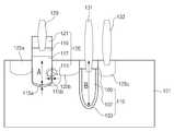
본 발명의 실시예에 따른 안티 퓨즈는 주변회로영역에 형성되며, 리세스 게이트 형태의 프로그램 게이트(120), 매립 게이트 형태의 셀렉트 게이트(110), 소스/드레인 영역(125a, 125b, 125c), 제 1 메탈콘택(129), 제 2 메탈콘택(131), 제 3 메탈콘택(133)을 포함한다.The anti-fuse according to the exemplary embodiment of the present invention is formed in the peripheral circuit region, and includes a
셀렉트 게이트(110)는 반도체 기판(101) 내에 형성된 트랜치 내에 순차적으로 적층된 게이트 절연막(103), 도전막(107), 하드마스크막(109)을 포함한다. 이때, 셀렉트 게이트(110)는 셀 영역(미도시)의 매립 게이트와 동시에 형성될 수 있으며 셀 영역(미도시)의 매립 게이트와 동일한 깊이(B) 및 크기를 갖도록 형성될 수 있고, 게이트 절연막(103)의 두께가 셀 영역(미도시)의 매립 게이트에 구비되는 게이트 절연막의 두께와 동일하게 형성될 수 있다.The
프로그램 게이트(120)는 순차적으로 적층된 게이트 절연막(115), 도전막(117), 도전막(119) 및 하드마스크막(121)을 포함한다. 이때, 게이트 절연막(115) 및 도전막(117)은 반도체 기판 내에 형성된 리세스 내에 구비되고, 도전막(119) 및 하드마스크막(121)은 도전막(117)의 상부에 형성되어 패터닝된다. 즉, 도전막(119) 및 하드마스크막(121)은 반도체 기판 상부에 형성된다. 또한, 프로그램 게이트(120)는 센스앰프 영역(미도시)의 리세스 게이트 형성 시 동시에 형성될 수 있으며, 반도체 기판(101) 내에 형성되는 리세스가 셀렉트 게이트(110)보다 얕은 깊이(A)로 형성되도록 한다. 이에, 프로그램 게이트(120)의 채널 길이가 짧아져 파열 산포 특성을 개선할 수 있다.The
또한, 프로그램 게이트(120)의 게이트 절연막(115)은 셀렉트 게이트(110)의 게이트 절연막(103)보다 얇은 두께로 형성하여 파열이 용이하도록 한다. 또한, 프로그램 게이트(120)의 게이트 절연막(115) 형성 시 리세스의 바닥면의 게이트 절연막(115a)은 두껍게 형성하고 리세스의 양측벽의 게이트 절연막(115b)은 얇게 형성함으로써 양측벽의 게이트 절연막(115b)이 파열되기 용이하도록 할 수 있다. 또한, 프로그램 게이트(120)의 트랜치의 하부가 각지도록 형성함으로써 트랜치 하부의 모서리지점의 게이트 절연막(115)의 파열이 용이하도록 할 수도 있다. 이때, 트랜치 하부가 각지도록 형성하는 것은 트랜치 하부 바닥면이 평평하게 형성되어 트랜치 하부 바닥면과 트랜치의 측벽이 만나는 지점(모서리)이 각지도록 형성되는 것을 의미한다.In addition, the
소스/드레인 영역(125a, 125b, 125c)은 프로그램 게이트(120)와 셀렉트 게이트(110)를 포함하는 구조물의 노출된 반도체 기판(101)에 이온을 주입하여 형성된 다. 이때, 반도체 기판(101)이 Pwell 인 경우 소스/드레인 영역(125a, 125b, 125c)에는 N+이온을 주입하여 형성할 수 있다.The source/
제 1 메탈콘택(129)은 프로그램 게이트(120)에 접속되고, 제 2 메탈콘택(131)은 셀렉트 게이트(110)에 접속되며, 제 3 메탈콘택(133)은 소스/드레인영역(125c)에 접속된다. 이에, 제 1 메탈콘택(129)에 고전압이 인가되고 제 2 메탈콘택(131)에 저전압이 인가되면 프로그램 게이트(120)가 파열되면서 흐르는 전류가 제 3 메탈콘택(133)을 통해 흐르게 된다.The
이와 같이, 본 발명의 실시예에 따른 안티퓨즈는 프로그램 게이트(120)를 리세스 게이트 구조로 형성하고 셀렉트 게이트(110)를 매립 게이트 구조로 형성한다. 또한, 프로그램 게이트(120)의 깊이(A)가 셀렉트 게이트(110)의 깊이(B) 보다 얕게 형성되도록 하여, 셀렉트 게이트(110)의 채널길이를 증가시켜 셀렉트 게이트(110)의 특성을 개선하는 동시에 프로그램 게이트(120)의 채널길이는 감소시켜 프로그램 게이트(120)의 파열 특성을 개선할 수 있다. 또한, 프로그램 게이트(120)를 리세스 게이트 구조로 형성하고 셀렉트 게이트(110)를 매립 게이트 구조로 형성함으로써 게이트 자체 폭이 좁아져 프로그램 게이트와 셀렉트 게이트 간의 간격이 넓어지게 되어 저항성이 커져서, 프로그램 게이트의 게이트 절연막 파열 시 급격하게 흐르는 전류에 의해 셀렉트 게이트가 영향을 덜 받을 수 있다.As described above, in the anti-fuse according to an embodiment of the present invention, the
도 2를 참조하여 프로그램 게이트(120) 파열 시의 안티퓨즈의 동작을 설명하면 아래와 같다.An operation of the antifuse when the
즉, 셀렉트 게이트(110)에 저전압이 인가되고 프로그램 게이트(120)에 고전압이 인가되면 게이트 절연막(115)이 파열되고, 화살표 방향과 같이 소스/드레인 영역(125b) 및 셀렉트 게이트(110) 하부를 통해 소스/드레인 영역(125c)까지 채널 영역이 형성되어 전류가 제 3 메탈콘택(133)을 통해 출력된다.That is, when a low voltage is applied to the
도 3은 본 발명의 다른 실시예에 따른 안티퓨즈의 단면도이다.3 is a cross-sectional view of an antifuse according to another embodiment of the present invention.
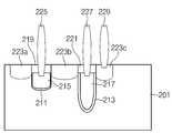
본 발명의 다른 실시예에 따른 안티 퓨즈는 매립 게이트 구조의 프로그램 게이트(210), 매립 게이트 구조의 셀렉트 게이트(220), 소스/드레인 영역(223a, 223b, 223c), 제 1 메탈콘택(225), 제 2 메탈콘택(227), 제 3 메탈콘택(229)을 포함한다.The anti-fuse according to another embodiment of the present invention includes a
프로그램 게이트(210)는 반도체 기판(201) 내에 형성된 트랜치 내에 적층되는 게이트 절연막(211), 도전막(215), 및 하드마스크막(219)을 포함한다. 이때, 게이트 절연막(211)과 도전막(215)은 트랜치의 측벽 하부에 형성되고 트랜치의 상부(upper portion) 전면에 하드마스크막(219)이 형성된다. 또한, 프로그램 게이트(210)의 게이트 절연막(211)은 셀렉트 게이트(220)의 게이트 절연막(213)보다 얇은 두께로 형성하여 파열이 용이하도록 한다. 또한, 프로그램 게이트(210)의 트랜치의 하부가 각지도록 형성함으로써 트랜치 하부의 모서리지점의 게이트 절연막(211)의 파열이 용이하도록 할 수 있다. 도 3에 도시되진 않았지만 프로그램 게이트(210)의 게이트 절연막(211) 형성 시 트랜치의 바닥면의 게이트 절연막(211)은 두껍게 형성하고 트랜치의 양측벽의 게이트 절연막(211)은 얇게 형성함으로써 양측벽의 게이트 절연막(211)이 파열되기 용이하도록 형성할 수도 있다.The
셀렉트 게이트(220)는 반도체 기판(201) 내에 형성된 트랜치 내에 적층되는 게이트 절연막(213), 도전막(217), 및 하드마스크막(221)을 포함한다. 이때, 셀렉트 게이트(220)는 셀 영역(미도시)의 매립 게이트와 동시에 형성될 수 있으며 셀 영역(미도시)의 매립 게이트와 동일한 깊이 및 크기를 갖도록 형성될 수 있다.The
이때, 프로그램 게이트(210)의 깊이(C)는 셀렉트 게이트(220)의 깊이(D)보다 얕은 깊이로 형성될 수 있고, 프로그램 게이트(210)의 채널 길이가 짧아져 파열 산포 특성을 개선할 수 있다. 또한, 셀렉트 게이트(220)는 깊이가 깊은 매립 게이트 구조로 형성함으로써 채널 길이가 증가되어 소자 신뢰도를 개선할 수 있다.At this time, the depth C of the
소스/드레인 영역(223a, 223b, 223c)은 프로그램 게이트(210)와 셀렉트 게이트(220)를 포함하는 구조물의 노출된 반도체 기판(201)에 이온을 주입하여 형성된 다. 이때, 반도체 기판(201)이 Pwell 인 경우 소스/드레인 영역(223a, 223b, 223c)에는 N+이온을 주입하여 형성할 수 있다.The source/
제 1 메탈콘택(225)은 프로그램 게이트(210)에 접속되고, 제 2 메탈콘택(227)은 셀렉트 게이트(220)에 접속되며, 제 3 메탈콘택(229)은 소스/드레인영역(125c)에 접속된다.The
이와 같이, 본 발명의 다른 실시예에 따른 안티퓨즈는 프로그램 게이트(210)를 매립 게이트 구조로 형성하고 셀렉트 게이트(220)도 매립 게이트 구조로 형성한다. 이에, 프로그램 게이트(210)와 셀렉트 게이트(220) 자체 폭을 좁게 형성함에 따라 프로그램 게이트(210)와 셀렉트 게이트(220) 사이의 간격이 커져서 파열 시 과도한 전류가 흐르게 될 때 프로그램 게이트(210)와 셀렉트 게이트(220)의 간격이 저항 역할을 하여 셀렉트 게이트(220)의 신뢰성을 개선할 수 있다. 또한, 프로그램 게이트(210)의 깊이(C)가 셀렉트 게이트(220)의 깊이(D) 보다 얕은 깊이를 갖도록 형성하여, 셀렉트 게이트(220)의 채널길이는 증가시켜 셀렉트 게이트(220)의 특성을 개선하는 동시에 프로그램 게이트(210)의 채널길이는 감소시켜 프로그램 게이트(210)의 파열 특성을 개선할 수 있다.As described above, in the anti-fuse according to another embodiment of the present invention, the
도 4를 참조하여, 프로그램 게이트(210) 파열 시의 안티퓨즈의 동작을 설명하면 아래와 같다. 즉, 셀렉트 게이트(220)에 저전압이 인가되고 프로그램 게이트(210)에 고전압이 인가되면 게이트 절연막(211)이 파열되고, 화살표 방향과 같이 소스/드레인 영역(223b), 셀렉트 게이트(220) 하부를 통해 소스/드레인 영역(223c)까지 채널 영역이 형성되어 전류가 제 3 메탈콘택(229)을 통해 출력된다.Referring to FIG. 4, the operation of the anti-fuse when the
이와 같이, 본 발명은 셀렉트 게이트와 프로그램 게이트를 플래너 게이트가 아닌 매립 게이트 구조로 형성함으로써, 게이트 자체 폭이 좁아져 게이트 간의 간격이 증가된다. 이에, 게이트 간의 간격이 저항 역할을 하여 프로그램 게이트의 파열 시 흐르는 과도한 전류가 셀렉트 게이트에 미치는 영향을 최소화할 수 있다.As described above, according to the present invention, since the select gate and the program gate are formed in a buried gate structure instead of a planar gate, the width of the gate itself is narrowed and the gap between the gates is increased. Accordingly, since the gap between the gates serves as a resistor, the influence of an excessive current flowing when the program gate is ruptured on the select gate can be minimized.
또한, 본 발명은 프로그램 게이트와 셀렉트 게이트의 게이트 절연막의 두께를 다르게 형성한다. 즉, 셀렉트 게이트의 게이트 절연막은 두껍게 형성하고 프로그램 게이트의 게이트 절연막은 얇게 형성함으로서 프로그램 게이트의 게이트 절연막의 파열이 용이하고 셀렉트 게이트의 게이트 절연막은 파열 시 흐르게 되는 급격한 전류의 영향을 덜 받게 된다.Further, according to the present invention, the thickness of the gate insulating film of the program gate and the select gate is formed differently. That is, since the gate insulating layer of the select gate is formed thick and the gate insulating layer of the program gate is formed thin, the gate insulating layer of the program gate is easily ruptured, and the gate insulating layer of the select gate is less affected by the rapid current flowing when the select gate is ruptured.
또한, 본 발명은 셀렉트 게이트와 프로그램 게이트의 깊이를 다르게 형성할 수 있다. 셀렉트 게이트의 깊이를 깊게 형성할수록 채널 길이가 길어져 셀렉트 게이트의 소자 특성을 향상시킬 수 있는 반면에, 프로그램 게이트는 채널 길이가 길어질 수록 파열 산포가 나빠지는 특성을 가지므로 프로그램 게이트의 깊이를 낮게 형성함으로써 프로그램 게이트의 채널 길이가 짧아져 파열 산포 특성을 개선할 수 있다.In addition, according to the present invention, the select gate and the program gate may have different depths. The deeper the depth of the select gate is, the longer the channel length, which improves the device characteristics of the select gate. On the other hand, the program gate has a property of worsening the rupture distribution as the channel length increases. Since the channel length of the program gate is shortened, the burst distribution characteristics can be improved.
이하, 도 5a 내지 도 5f를 참조하여, 본 발명의 실시예에 따른 안티 퓨즈의 제조 방법을 설명하기로 한다.Hereinafter, a method of manufacturing an anti-fuse according to an embodiment of the present invention will be described with reference to FIGS. 5A to 5F.
먼저, 도 5a에 도시된 바와 같이, 반도체 기판(101) 상에 매립 게이트 형성을 위한 마스크(105)를 형성하고, 마스크(105)에 의해 노출된 반도체 기판(101)을 식각하여 매립 게이트 형성을 위한 트랜치(102)를 형성한다.First, as shown in FIG. 5A, a
도 5b를 참조하면, 트랜치(102)를 포함하는 전체 구조물의 단차를 따라 게이트 절연막(103)을 증착한 후 평탄화 공정을 수행하여 게이트 절연막(103)이 트랜치(102) 내에만 남겨지도록 형성한다. 이때, 트랜치(102)는 셀렉트 게이트용으로서 게이트 절연막(103)을 셀 영역(미도시)의 매립 게이트 형성시의 게이트 절연막과 동일한 두께로 형성하는 것이 바람직하다.Referring to FIG. 5B, after depositing the
이어서, 트랜치(102) 내의 게이트 절연막(103) 상부에 도전물질을 매립한 후 에치백 공정을 수행하여 게이트 절연막(103) 및 도전막(107)의 일부를 제거하여 트랜치(102) 하부 측벽 및 바닥면에 게이트 절연막(103)과 도전막(107)을 형성한다.Subsequently, a conductive material is buried in the upper portion of the
이어서, 도전막(107)의 상부에 하드마스크 물질을 증착한 후 평탄화 공정을 수행하여 반도체 기판(101)의 상부의 하드마스크 물질을 제거하여 반도체 기판(101)의 상부면이 노출되도록 하고, 도전막(107) 상부에 하드마스크막(109)이 형성된다. 이에, 도전막(107) 및 하드마스크막(109)로 구성된 매립 게이트가 셀렉트 게이트(110)가 된다. 이때, 도전막(107)은 텅스텐(W), 티타늄(Ti), 티타늄 질화막(TiN)과 같은 금속이나 폴리실리콘(poly-silicon)을 포함할 수 있고, 하드마스크막(109)은 캡핑막(capping)으로서 질화막이나 산화막(Oxide)을 포함할 수 있고, 게이트 절연막(103)은 산화막(Oxide)으로 형성될 수 있다.Subsequently, after depositing a hard mask material on the top of the
또한, 매립 게이트 구조의 셀렉트 게이트(110)의 게이트 절연막(103)은 셀렉트 게이트의 특성을 위해 두꺼운 두께를 가지도록 하는 것이 바람직하다. 즉, 셀렉트 게이트(110)의 두께를 두껍게 형성함으로써 퓨즈 파열 시 흘러들어오는 전류의 영향을 덜 받을 수 있어 셀렉트 게이트(110)의 소자 특성이 개선될 수 있다. 또한, 셀렉트 게이트(110)를 매립 게이트 구조로 형성함으로써 셀렉트 게이트(110)의 채널길이가 플래너 게이트의 채널길이보다 길어져 셀렉트 게이트(110)의 특성을 개선시킬 수 있다.In addition, it is preferable that the
도 5c를 참조하면, 프로그램 게이트를 형성하기 위해, 셀렉트 게이트(110)를 포함하는 구조물 상부에 프로그램 게이트 형성을 위한 마스크(111)를 형성하고 셀렉트 게이트(110)와 이웃하는 위치의 노출된 반도체 기판(101)을 식각하여 리세스(113)를 형성한다. 이때, 리세스(113)의 깊이(A)는 도 5a에서의 셀렉트 게이트용 트랜치(102)의 깊이(B)보다 얕은 깊이를 가지도록 형성한다.Referring to FIG. 5C, in order to form a program gate, a
이어서 리세스(113)를 포함하는 전체 구조물의 단차를 따라 게이트 절연막(115)을 증착한 후 평탄화 공정을 수행하여 게이트 절연막(115)이 리세스(113) 내에만 남겨지도록 형성한다. 이때, 리세스(113)의 바닥면의 게이트 절연막(115a)은 두껍게 남겨지고 리세스(113)의 측벽의 게이트 절연막(115b)은 얇게 남겨져 측벽의 게이트 절연막(115b)의 파열이 더 용이하도록 하는 것이 바람직하다. 또한, 프로그램 게이트용 리세스(113)는 센스앰프영역(미도시)의 리세스 게이트 형성 시에 동시에 패터닝하여 형성할 수 있다.Subsequently, the
도 5d를 참조하면, 리세스(113)의 게이트 절연막(115)을 에치백하여 슬림화하고, 리세스(113) 측벽 상부의 게이트 절연막(115)의 일부를 제거하여 게이트 절연막(115)이 리세스(113)의 하부 측벽 및 바닥면에만 남도록 한다. 그 후, 리세스(113)를 포함하는 구조물 상부에 도전막(117, 119) 및 하드마스크막(121)을 순차적으로 적층한 후 패터닝하여 프로그램 게이트(120)를 형성한다. 이때, 도전막(117)은 리세스(113)를 매립하고 도전막(119) 및 하드마스크막(121)은 그 상부에 형성되어 반도체 기판(101) 상부에 형성된다.Referring to FIG. 5D, the
또한, 프로그램 게이트(120)의 게이트 절연막(115)은 셀렉트 게이트(110)의 게이트 절연막(103)에 비해 얇게 형성되도록 하여 파열이 용이하도록 하는 것이 바람직하다.In addition, it is preferable that the
도 5e를 참조하면, 노출된 반도체 기판(101)에 이온을 주입하여 소스/드레인 영역(125a, 125b, 125c)을 형성한다. 이때, 반도체 기판(101)이 P well인 경우 소스/드레인 영역(125a, 125b, 125c)에 N+ 이온을 주입하도록 한다.Referring to FIG. 5E, ions are implanted into the exposed
도 5f를 참조하면, 프로그램 게이트(120) 및 셀렉트 게이트(110) 상부에 제 1 메탈콘택(129), 제 2 메탈콘택(131)을 각각 형성하고 소스/드레인 영역(125c) 상부에 제 3 메탈콘택(133)이 각각 형성된다.Referring to FIG. 5F, a
이때, 제 1 메탈콘택(129), 제 2 메탈콘택(131), 제 3 메탈콘택(133)은 셀렉트 게이트(110)와 프로그램 게이트(120)를 포함하는 반도체 기판 전면에 층간절연막(미도시)을 증착한 후, 층간절연막(미도시)을 식각하여 콘택홀(미도시)을 형성하고 나서 콘택홀(미도시)에 도전물질을 증착함으로써 형성된다. At this time, the
여기서, 셀렉트 게이트(110)에 제 2 메탈콘택(131) 형성 시에는, 하드마스크막(109) 및 도전막(107)의 일부까지 식각하여 메탈콘택홀(미도시)을 형성하도록 함으로써, 제 2 메탈콘택(131)이 도전막(107)에 접속되도록 한다. 또한, 프로그램 게이트(120)에 제 1 메탈콘택(129)이 형성되는 경우 하드마스크막(121) 및 도전막(119)의 일부까지 식각하여 메탈콘택홀(미도시)을 형성하도록 함으로써, 제 1 메탈콘택(129)이 도전막(119)에 접속되도록 한다.Here, when the
이와 같이, 본 발명의 실시예는 프로그램 게이트(120)는 리세스 게이트 구조로 형성하고 셀렉트 게이트(110)는 매립 게이트 구조로 형성하여 게이트의 폭을 좁게 형성하여 게이트 간의 간격을 증가시킴으로써 프로그램 게이트(120)의 게이트 절연막 파열 시 흐르게 되는 과도한 전류의 영향을 셀렉트 게이트(110)가 덜 받을 수 있도록 하여 셀렉트 게이트(110)의 특성을 개선할 수 있다.As described above, according to the exemplary embodiment of the present invention, the
또한, 프로그램 트랜지스터의 게이트 절연막은 얇게 형성하여 파열이 용이하도록 하는 동시에 셀렉트 트랜지스터의 게이트 절연막은 두껍게 형성함으로써 셀렉트 트랜지스터의 신뢰성을 향상시킬 수 있다. 또한, 셀렉트 게이트(110)와 프로그램 게이트(120)의 깊이를 다르게 형성함으로써, 셀렉트 게이트(110)의 채널 길이는 증가시켜 셀렉트 게이트(110)의 소자 특성을 개선하고 프로그램 게이트(120)의 채널 길이는 감소시켜 프로그램 게이트의 파열 분포 특성을 개선할 수 있다.In addition, since the gate insulating film of the program transistor is formed thin to facilitate rupture, while the gate insulating film of the select transistor is formed thick, reliability of the select transistor can be improved. In addition, by forming different depths of the
이하, 도 6a 내지 도 6f를 참조하여, 본 발명의 다른 실시예에 따른 안티 퓨즈의 제조 방법을 설명하기로 한다.Hereinafter, a method of manufacturing an anti-fuse according to another embodiment of the present invention will be described with reference to FIGS. 6A to 6F.
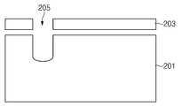
도 6a를 참조하면, 반도체 기판(201) 상부에 프로그램 게이트 형성을 위한 마스크(203)를 형성하고, 마스크(203)에 의해 노출된 반도체 기판을 식각하여 프로그램 게이트 형성을 위한 트랜치(205)를 형성한다. 이때, 트랜치(205)의 프로파일을 각지게 형성하여 모서리에 필드가 집중되어 게이트 절연막(미도시)이 잘 파열되도록 하는 것이 바람직하다.6A, a
도 6b를 참조하면, 반도체 기판(201) 상부에 셀렉트 게이트 형성을 위한 마스크(207)를 형성하고, 마스크(207)에 의해 노출된 반도체 기판을 식각하여 트랜치(209)를 형성한다. 또한, 셀렉트 게이트 형성을 위한 트랜치(207)는 셀영역(미도시)의 매립 게이트 형성 시 동시에 형성하는 것이 바람직하다. 도 6a 및 도 6b에서와 같이 프로그램 게이트용 트랜치(205)를 먼저 형성하고 셀렉트 게이트용 트랜치(207)를 형성하는 경우 에치백 후 클린 공정이 2번 적용되어 반도체 기판(101)의 표면 특성이 나빠져 프로그램 게이트의 게이트 절연막(미도시) 파열이 더 유리해질 수 있다.Referring to FIG. 6B, a
또한, 셀렉트 게이트 형성을 위한 트랜치(209)의 깊이(D)가 프로그램 게이트 형성을 위한 트랜치(205)의 깊이(C)보다 더 깊게 형성하는 것이 바람직하다. 즉, 셀렉트 게이트의 깊이를 깊게 형성함으로써 채널 길이를 증가시켜 셀렉트 게이트의 소자 특성을 개선하는 동시에 프로그램 게이트의 깊이를 낮게 형성함으로써 채널 길이를 감소시켜 프로그램 게이트의 파열 분포 특성을 개선할 수 있다.In addition, it is preferable that the depth (D) of the
도 6c를 참조하면, 트랜치(205, 207)을 포함하는 구조물 전면에 게이트 절연막을 증착한 후 평탄화 공정을 수행하여 게이트 절연막(211, 213)이 트랜치(205, 207)의 바닥면 및 양측벽에만 남도록 형성한다. 이때, 본 발명의 실시예와 같이 트랜치 바닥면의 게이트 절연막을 두껍게 형성하고 트랜치 측벽의 게이트 절연막을 얇게 형성하여 측벽의 게이트 절연막에 전자가 집중하여 파열이 용이하도록 형성할 수도 있다.Referring to FIG. 6C, after depositing a gate insulating film on the entire surface of the structure including the
도 6d를 참조하면, 트랜치(205, 207) 내 게이트 절연막(211, 213) 상부에 도전물질을 매립하여 도전막(215, 217)을 각각 형성하고 도전막(215, 217) 상부에 하드마스크막(219, 221)을 순차적으로 적층한다. 이에, 반도체 기판(201) 내에 깊이가 다른 프로그램 게이트(210)와 셀렉트 게이트(220)가 형성된다.Referring to FIG. 6D,
도 6e를 참조하면, 프로그램 게이트(210)와 셀렉트 게이트(220)를 포함하는 구조물에서 노출된 반도체 기판(201) 상에 이온을 주입하여 소스/드레인 영역(223a, 223b, 223c)을 형성한다. 이때, 반도체 기판(201)이 P well인 경우 소스/드레인 영역(223a, 223b, 223c)에 N+ 이온을 주입할 수 있다.Referring to FIG. 6E, source/
도 6f를 참조하면, 매립 게이트(210, 220) 상부에 제 1 메탈콘택(225), 제 2 메탈콘택(227)을 각각 형성하고 소스/드레인 영역(223c) 상부에 제 3 메탈콘택(229)이 각각 형성된다.6F, a
이때, 제 1 메탈콘택(225), 제 2 메탈콘택(227), 제 3 메탈콘택(229)은 매립 게이트(210, 220)를 포함하는 반도체 기판 전면에 층간절연막(미도시)을 증착한 후, 층간절연막(미도시)을 식각하여 콘택홀(미도시)을 형성하고나서 콘택홀(미도시)에 도전물질을 증착함으로써 형성된다. At this time, after depositing an interlayer insulating film (not shown) on the entire surface of the semiconductor substrate including the buried
여기서, 매립 게이트(210, 220)에 제 1 메탈콘택(225), 제 2 메탈콘택(227) 형성 시에는, 하드마스크막(219, 221) 및 도전막(215, 217)의 일부까지 식각하여 콘택홀(미도시)을 형성하도록 함으로써, 제 1 메탈콘택(225), 제 2 메탈콘택(227)이 도전막(215, 217)에 접속되도록 한다.Here, when forming the
이와 같이, 본 발명은 프로그램 게이트와 셀렉트 게이트를 구비하는 안티퓨즈에 관한 것으로서, 프로그램 게이트를 리세스 게이트 또는 매립 게이트 구조로 형성하고, 셀렉터 게이트를 매립 게이트 구조로 형성한다.As described above, the present invention relates to an antifuse having a program gate and a select gate, wherein the program gate is formed in a recess gate or a buried gate structure, and the selector gate is formed in a buried gate structure.
이에, 본 발명은 프로그램 게이트와 셀렉트 게이트 간의 간격이 증가하여 프로그램 게이트의 파열 시 프로그램 게이트에서 셀렉트 게이트로 흐르는 과도한 전류가 약해져 셀렉트 게이트의 신뢰성을 개선할 수 있다. 또한, 본 발명은 셀렉트 게이트의 깊이는 깊게 형성하고 프로그램 게이트의 깊이는 얕게 형성함으로써 셀렉트 게이트의 채널길이를 증가시켜 셀렉트 게이트의 특성을 개선하고 프로그램 게이트의 채널길이는 감소시켜 프로그램 게이트의 파열 산포 특성을 개선할 수 있다.Accordingly, according to the present invention, an excessive current flowing from the program gate to the select gate is weakened when the program gate is ruptured due to an increase in the distance between the program gate and the select gate, thereby improving reliability of the select gate. In addition, in the present invention, the depth of the select gate is formed to be deep and the depth of the program gate is formed to be shallow, so that the channel length of the select gate is increased to improve the characteristics of the select gate, and the channel length of the program gate is reduced to reduce the burst distribution characteristics of the program gate. Can be improved.
또한, 본 발명은 셀렉트 게이트의 게이트 절연막의 두께는 두껍게 형성하여 프로그램 게이트 파열 시 과도한 전류에 의한 영향을 최소화하고, 프로그램 게이트의 게이트 절연막의 두께를 얇게 형성함으로써, 프로그램 게이트의 파열을 용이하게 할 수 있다.In addition, the present invention minimizes the influence of excessive current when the program gate is ruptured by forming a thick gate insulating film of the select gate, and by forming a thin thickness of the gate insulating film of the program gate, it is possible to facilitate the rupture of the program gate. have.
또한, 프로그램 게이트 형성 시 리세스 또는 트랜치 하부의 모양을 각지게 형성하여 모서리 부분에서의 파열이 용이하게 할 수 있고, 리세스 또는 트랜치 바닥의 게이트 절연막은 두껍게 형성하고 리세스 또는 트랜치 측벽의 게이트 절연막은 얇게 형성하여 파열이 용이하도록 할 수 있다.In addition, when the program gate is formed, the shape of the bottom of the recess or trench can be formed to be angled to facilitate rupture at the edge. The gate insulating layer at the bottom of the recess or trench is formed thick, and the gate insulating layer on the sidewall of the recess or trench Can be formed to be thin to facilitate rupture.
이상의 설명은 본 발명의 기술 사상을 예시적으로 설명한 것에 불과한 것으로서, 본 발명이 속하는 기술 분야에서 통상의 지식을 가진 자라면 본 발명의 본질적인 특성에서 벗어나지 않는 범위에서 다양한 수정 및 변형이 가능할 것이다. 따라서, 본 발명에 개시된 실시예들은 본 발명의 기술 사상을 한정하기 위한 것이 아니라 설명하기 위한 것이고, 이러한 실시예에 의하여 본 발명의 기술 사상의 범위가 한정되는 것은 아니다. 본 발명의 보호 범위는 아래의 청구범위에 의하여 해석되어야 하며, 그와 동등한 범위 내에 있는 모든 기술 사상은 본 발명의 권리범위에 포함되는 것으로 해석되어야 할 것이다.The above description is merely illustrative of the technical idea of the present invention, and those of ordinary skill in the art to which the present invention pertains will be able to make various modifications and variations without departing from the essential characteristics of the present invention. Accordingly, the embodiments disclosed in the present invention are not intended to limit the technical idea of the present invention, but to explain the technical idea, and the scope of the technical idea of the present invention is not limited by these embodiments. The scope of protection of the present invention should be interpreted by the following claims, and all technical ideas within the scope equivalent thereto should be interpreted as being included in the scope of the present invention.
101, 201 : 반도체 기판
115, 103, 211, 213 : 게이트 절연막
117, 119, 107, 211, 217 : 도전막
121, 109, 221, 219: 하드마스크막
102, 113, 205, 207 : 트랜치
125a, 125b, 125c, 223a, 223b, 223c : 소스/드레인 영역
129, 131, 133, 225, 227, 229 : 메탈콘택101, 201: semiconductor substrate
115, 103, 211, 213: gate insulating film
117, 119, 107, 211, 217: conductive film
121, 109, 221, 219: hard mask film
102, 113, 205, 207: trench
125a, 125b, 125c, 223a, 223b, 223c: source/drain area
129, 131, 133, 225, 227, 229: Metal contact
Claims (20)
Translated fromKorean상기 프로그램 게이트와 일정 간격 이격되어 상기 반도체 기판 내에 제2 깊이로 형성되는 셀렉트 게이트를 포함하고,
상기 제1 깊이는 상기 제2 깊이보다 얕고,
상기 프로그램 게이트의 제1 채널 길이는 상기 셀렉트 게이트의 제2 채널 길이보다 짧은 안티퓨즈.A program gate formed by being buried to a first depth in a semiconductor substrate in the peripheral circuit region; and
And a select gate spaced apart from the program gate and formed to a second depth in the semiconductor substrate,
The first depth is shallower than the second depth,
An antifuse having a first channel length of the program gate shorter than a second channel length of the select gate.
상기 프로그램 게이트 및 상기 셀렉트 게이트에 각각 연결되도록 형성된 제 1 및 제 2 메탈콘택; 및
상기 프로그램 게이트에 연결된 드레인영역 또는 소스영역 상에 형성되는 제 3 메탈콘택
을 더 포함하는 안티퓨즈.The method according to claim 1,
First and second metal contacts formed to be connected to the program gate and the select gate, respectively; And
A third metal contact formed on a drain region or a source region connected to the program gate
Antifuse further comprising.
상기 프로그램 게이트는,
상기 반도체 기판 내에 형성된 트랜치 내에 형성된 제 1 게이트 절연막;
상기 제 1 게이트 절연막 상부의 트랜치 내부를 채우는 제1 도전막; 및
상기 제 1 도전막 상부에 형성되어 상기 트랜치를 매립하는 제 1 하드마스크막
을 포함하는 것을 특징으로 하는 안티퓨즈.The method according to claim 1,
The program gate,
A first gate insulating layer formed in a trench formed in the semiconductor substrate;
A first conductive layer filling the inside of the trench over the first gate insulating layer; And
A first hard mask layer formed on the first conductive layer to fill the trench
Anti-fuse comprising a.
상기 셀렉트 게이트는,
상기 반도체 기판 내에 형성된 트랜치 내에 형성된 제 2 게이트 절연막;
상기 제 2 게이트 절연막 상부의 트랜치 내부를 채우는 제 2 도전막; 및
상기 제 2 도전막 상부에 형성된 제 2 하드마스크막
을 포함하는 것을 특징으로 하는 안티퓨즈.The method of claim 5,
The select gate,
A second gate insulating layer formed in a trench formed in the semiconductor substrate;
A second conductive layer filling the inside of the trench over the second gate insulating layer; And
A second hard mask layer formed on the second conductive layer
Anti-fuse comprising a.
상기 제 1 게이트 절연막은 상기 제 2 게이트 절연막보다 얇은 두께를 가지는 것을 특징으로 하는 안티퓨즈.The method of claim 6,
The anti-fuse, wherein the first gate insulating layer has a thickness thinner than that of the second gate insulating layer.
상기 제 2 게이트 절연막은 반도체 소자의 셀 영역의 매립 게이트 하부에 형성되는 게이트 절연막의 두께와 동일한 것을 특징으로 하는 안티퓨즈.The method of claim 6,
Wherein the second gate insulating layer is the same as the thickness of the gate insulating layer formed under the buried gate of the cell region of the semiconductor device.
상기 제 1 게이트 절연막이 파열(rupture)되면 상기 제 2 게이트 절연막 하부를 통해 채널이 형성되는 것을 특징으로 하는 안티퓨즈.The method of claim 6,
When the first gate insulating layer is ruptured, a channel is formed under the second gate insulating layer.
상기 반도체 기판 내에 제2 깊이로 매립되어 형성되는 셀렉트 게이트를 포함하고,
상기 제1 깊이는 상기 제2 깊이보다 얕고,
상기 프로그램 게이트의 제1 채널 길이는 상기 셀렉트 게이트의 제2 채널 길이보다 짧은 안티퓨즈.A program gate formed on a semiconductor substrate in a peripheral circuit region to a first depth and including a recess gate in the semiconductor substrate; And
And a select gate formed by being buried to a second depth in the semiconductor substrate,
The first depth is shallower than the second depth,
An antifuse having a first channel length of the program gate shorter than a second channel length of the select gate.
상기 프로그램 게이트는,
상기 반도체 기판 내에 형성된 리세스 내에 형성된 제 1 게이트 절연막;
상기 제 1 게이트 절연막 상부의 리세스 내부를 모두 채우는 제 1 도전막;
상기 제 1 도전막 상부에 일정 패턴을 가지도록 형성한 제 2 도전막; 및
상기 제 2 도전막 상부에 형성된 제 2 하드마스크막
을 포함하는 안티퓨즈.The method of claim 10,
The program gate,
A first gate insulating film formed in a recess formed in the semiconductor substrate;
A first conductive layer filling all of the recesses on the first gate insulating layer;
A second conductive layer formed on the first conductive layer to have a predetermined pattern; And
A second hard mask layer formed on the second conductive layer
Antifuse containing.
상기 셀렉트 게이트는,
상기 반도체 기판 내에 형성된 트랜치 내에 형성된 제 2 게이트 절연막;
상기 제 2 게이트 절연막 상부의 트랜치 내부를 채우는 제2 도전막; 및
상기 도전막 상부에 형성되는 제 2 하드마스크막
을 포함하는 안티퓨즈.The method of claim 10,
The select gate,
A second gate insulating layer formed in a trench formed in the semiconductor substrate;
A second conductive layer filling the inside of the trench over the second gate insulating layer; And
A second hard mask layer formed on the conductive layer
Antifuse containing.
상기 프로그램 게이트와 일정 간격 이격되어 상기 반도체 기판 내에 제2 깊이로 매립된 셀렉트 게이트를 형성하는 단계를 포함하고,
상기 제1 깊이는 상기 제2 깊이보다 얕고,
상기 프로그램 게이트의 제1 채널 길이는 상기 셀렉트 게이트의 제2 채널 길이보다 짧은 것을 특징으로 하는 안티퓨즈 제조 방법.Forming a program gate buried to a first depth in a semiconductor substrate in a peripheral circuit region; And
And forming a select gate spaced apart from the program gate and buried to a second depth in the semiconductor substrate,
The first depth is shallower than the second depth,
The antifuse manufacturing method, wherein the first channel length of the program gate is shorter than the second channel length of the select gate.
상기 프로그램 게이트 및 상기 셀렉트 게이트 양측의 반도체 기판에 소스 또는 드레인 영역을 형성하는 단계;
상기 프로그램 게이트 및 상기 셀렉트 게이트 상부에 제 1 및 제 2 메탈콘택을 각각 형성하는 단계; 및
상기 소스 또는 드레인 영역 상에 제 3 메탈 콘택을 형성하는 단계
를 더 포함하는 안티퓨즈 제조 방법.The method of claim 15,
Forming a source or drain region in the semiconductor substrate on both sides of the program gate and the select gate;
Forming first and second metal contacts on the program gate and the select gate, respectively; And
Forming a third metal contact on the source or drain region
Antifuse manufacturing method further comprising a.
상기 프로그램 게이트를 형성하기 전에 상기 프로그램 게이트 하부에 제 1 게이트 절연막을 형성하고,
상기 셀렉트 게이트를 형성하기 전에 상기 셀렉트 게이트 하부에 제 2 게이트 절연막을 형성하되,
상기 제 1 게이트 절연막은 상기 제 2 게이트 절연막보다 얇은 두께를 가지도록 형성하는 것을 특징으로 하는 안티퓨즈 제조 방법.The method of claim 15,
Forming a first gate insulating layer under the program gate before forming the program gate,
Before forming the select gate, a second gate insulating layer is formed under the select gate,
The method of manufacturing an anti-fuse, wherein the first gate insulating layer is formed to have a thickness thinner than that of the second gate insulating layer.
상기 프로그램 게이트와 일정 간격 이격되어 상기 반도체 기판 내에 제2 깊이로 매립된 셀렉트 게이트를 형성하는 단계를 포함하고,
상기 제1 깊이는 상기 제2 깊이보다 얕고,
상기 프로그램 게이트의 제1 채널 길이는 상기 셀렉트 게이트의 제2 채널 길이보다 짧은 것을 특징으로 하는 안티퓨즈 제조 방법.Forming a program gate including a recess gate at a first depth on the semiconductor substrate in the peripheral circuit region; And
And forming a select gate spaced apart from the program gate and buried to a second depth in the semiconductor substrate,
The first depth is shallower than the second depth,
The antifuse manufacturing method, wherein the first channel length of the program gate is shorter than the second channel length of the select gate.
Priority Applications (2)
| Application Number | Priority Date | Filing Date | Title |
|---|---|---|---|
| KR1020140017977AKR102191909B1 (en) | 2014-02-17 | 2014-02-17 | Anti-fuse and method for fabricating the same |
| US14/280,320US9490333B2 (en) | 2014-02-17 | 2014-05-16 | Anti-fuse and method for forming the same |
Applications Claiming Priority (1)
| Application Number | Priority Date | Filing Date | Title |
|---|---|---|---|
| KR1020140017977AKR102191909B1 (en) | 2014-02-17 | 2014-02-17 | Anti-fuse and method for fabricating the same |
Publications (2)
| Publication Number | Publication Date |
|---|---|
| KR20150097846A KR20150097846A (en) | 2015-08-27 |
| KR102191909B1true KR102191909B1 (en) | 2020-12-18 |
Family
ID=53798849
Family Applications (1)
| Application Number | Title | Priority Date | Filing Date |
|---|---|---|---|
| KR1020140017977AExpired - Fee RelatedKR102191909B1 (en) | 2014-02-17 | 2014-02-17 | Anti-fuse and method for fabricating the same |
Country Status (2)
| Country | Link |
|---|---|
| US (1) | US9490333B2 (en) |
| KR (1) | KR102191909B1 (en) |
Families Citing this family (7)
| Publication number | Priority date | Publication date | Assignee | Title |
|---|---|---|---|---|
| US10109740B2 (en)* | 2016-07-18 | 2018-10-23 | International Business Machines Corporation | Programmable bulk FinFET antifuses |
| KR102684720B1 (en)* | 2016-12-09 | 2024-07-12 | 삼성전자주식회사 | Anti-fuse device and memory device comprising the anti-fuse |
| KR102568407B1 (en) | 2018-06-27 | 2023-08-21 | 엘지전자 주식회사 | Vacuum adiabatic body and refrigerator |
| CN113496987B (en)* | 2020-04-08 | 2024-03-29 | 长鑫存储技术有限公司 | Antifuse device and antifuse unit |
| TWI770804B (en)* | 2021-02-04 | 2022-07-11 | 華邦電子股份有限公司 | Memory device and method for manufacturing the same |
| CN115188765B (en)* | 2021-04-02 | 2024-06-25 | 长鑫存储技术有限公司 | Semiconductor structure, method for manufacturing semiconductor structure and programming method |
| KR20240000599A (en)* | 2021-09-17 | 2024-01-02 | 창신 메모리 테크놀로지즈 아이엔씨 | Antifuse array structure and memory |
Citations (1)
| Publication number | Priority date | Publication date | Assignee | Title |
|---|---|---|---|---|
| KR100609524B1 (en)* | 2005-03-23 | 2006-08-08 | 주식회사 하이닉스반도체 | Method of forming a semiconductor device |
Family Cites Families (8)
| Publication number | Priority date | Publication date | Assignee | Title |
|---|---|---|---|---|
| US7795094B2 (en) | 2004-09-02 | 2010-09-14 | Micron Technology, Inc. | Recessed gate dielectric antifuse |
| KR20060066195A (en)* | 2004-12-13 | 2006-06-16 | 삼성전자주식회사 | Anti-fuse device and its manufacturing method |
| KR100680958B1 (en)* | 2005-02-23 | 2007-02-09 | 주식회사 하이닉스반도체 | Manufacturing method of PMOS transistor |
| US8338887B2 (en)* | 2005-07-06 | 2012-12-25 | Infineon Technologies Ag | Buried gate transistor |
| KR100771539B1 (en)* | 2005-12-29 | 2007-10-31 | 주식회사 하이닉스반도체 | Semiconductor device having recess gate and manufacturing method thereof |
| US8049299B2 (en)* | 2009-02-25 | 2011-11-01 | Freescale Semiconductor, Inc. | Antifuses with curved breakdown regions |
| KR20120120668A (en)* | 2011-04-25 | 2012-11-02 | 에스케이하이닉스 주식회사 | Antifuse and method for fabricating the same |
| KR101950002B1 (en)* | 2012-07-30 | 2019-02-20 | 에스케이하이닉스 주식회사 | Semiconductor device and method for fabricating the same |
- 2014
- 2014-02-17KRKR1020140017977Apatent/KR102191909B1/ennot_activeExpired - Fee Related
- 2014-05-16USUS14/280,320patent/US9490333B2/enactiveActive
Patent Citations (1)
| Publication number | Priority date | Publication date | Assignee | Title |
|---|---|---|---|---|
| KR100609524B1 (en)* | 2005-03-23 | 2006-08-08 | 주식회사 하이닉스반도체 | Method of forming a semiconductor device |
Also Published As
| Publication number | Publication date |
|---|---|
| US20150236154A1 (en) | 2015-08-20 |
| US9490333B2 (en) | 2016-11-08 |
| KR20150097846A (en) | 2015-08-27 |
Similar Documents
| Publication | Publication Date | Title |
|---|---|---|
| KR102191909B1 (en) | Anti-fuse and method for fabricating the same | |
| KR101102766B1 (en) | Manufacturing Method of Semiconductor Device | |
| US9558990B2 (en) | Semiconductor device and method for forming the same | |
| US11800702B2 (en) | Method of forming a memory device | |
| JP2013149686A (en) | Semiconductor device | |
| KR20110086357A (en) | Semiconductor device and manufacturing method | |
| JP2007180481A (en) | Semiconductor device having vertical channel and method of manufacturing the same | |
| KR20140016068A (en) | Semiconductor device and method for fabricating the same | |
| KR20140010271A (en) | Semiconductor device and manufacturing method of the same | |
| KR102573736B1 (en) | Fuse Structure and Method of Manufacturing The Same | |
| US20150214234A1 (en) | Semiconductor device and method for fabricating the same | |
| KR20140030483A (en) | Nonvolatile memory device and method for fabricating the same | |
| JP2007134669A (en) | Flash memory device and manufacturing method thereof | |
| KR20120012222A (en) | Semiconductor device manufacturing method | |
| KR100827509B1 (en) | Method of forming a semiconductor device | |
| KR20120004802A (en) | Semiconductor device manufacturing method | |
| KR20180006740A (en) | Semiconductor device and manufacturing method of the same | |
| KR100905830B1 (en) | Semiconductor element and manufacturing method thereof | |
| KR100929643B1 (en) | Semiconductor element and manufacturing method thereof | |
| KR101161747B1 (en) | Method for fabricating semiconductor device | |
| KR20120038070A (en) | Semiconductor device and method for fabricating the same | |
| KR20090025808A (en) | Semiconductor device formation method | |
| CN104766863A (en) | Three-dimensional memory and its manufacturing method | |
| KR20120127018A (en) | Method for manufacturing buried bit line in semiconductor device | |
| KR20140090447A (en) | Method for manufacturing semiconductor device |
Legal Events
| Date | Code | Title | Description |
|---|---|---|---|
| PA0109 | Patent application | St.27 status event code:A-0-1-A10-A12-nap-PA0109 | |
| PN2301 | Change of applicant | St.27 status event code:A-3-3-R10-R13-asn-PN2301 St.27 status event code:A-3-3-R10-R11-asn-PN2301 | |
| PG1501 | Laying open of application | St.27 status event code:A-1-1-Q10-Q12-nap-PG1501 | |
| A201 | Request for examination | ||
| PA0201 | Request for examination | St.27 status event code:A-1-2-D10-D11-exm-PA0201 | |
| D13-X000 | Search requested | St.27 status event code:A-1-2-D10-D13-srh-X000 | |
| D14-X000 | Search report completed | St.27 status event code:A-1-2-D10-D14-srh-X000 | |
| E902 | Notification of reason for refusal | ||
| PE0902 | Notice of grounds for rejection | St.27 status event code:A-1-2-D10-D21-exm-PE0902 | |
| E13-X000 | Pre-grant limitation requested | St.27 status event code:A-2-3-E10-E13-lim-X000 | |
| P11-X000 | Amendment of application requested | St.27 status event code:A-2-2-P10-P11-nap-X000 | |
| P13-X000 | Application amended | St.27 status event code:A-2-2-P10-P13-nap-X000 | |
| E701 | Decision to grant or registration of patent right | ||
| PE0701 | Decision of registration | St.27 status event code:A-1-2-D10-D22-exm-PE0701 | |
| PR0701 | Registration of establishment | St.27 status event code:A-2-4-F10-F11-exm-PR0701 | |
| PR1002 | Payment of registration fee | St.27 status event code:A-2-2-U10-U11-oth-PR1002 Fee payment year number:1 | |
| PG1601 | Publication of registration | St.27 status event code:A-4-4-Q10-Q13-nap-PG1601 | |
| PC1903 | Unpaid annual fee | St.27 status event code:A-4-4-U10-U13-oth-PC1903 Not in force date:20231211 Payment event data comment text:Termination Category : DEFAULT_OF_REGISTRATION_FEE | |
| PC1903 | Unpaid annual fee | St.27 status event code:N-4-6-H10-H13-oth-PC1903 Ip right cessation event data comment text:Termination Category : DEFAULT_OF_REGISTRATION_FEE Not in force date:20231211 | |
| P22-X000 | Classification modified | St.27 status event code:A-4-4-P10-P22-nap-X000 |