KR102185787B1 - Display device - Google Patents
Display deviceDownload PDFInfo
- Publication number
- KR102185787B1 KR102185787B1KR1020130158201AKR20130158201AKR102185787B1KR 102185787 B1KR102185787 B1KR 102185787B1KR 1020130158201 AKR1020130158201 AKR 1020130158201AKR 20130158201 AKR20130158201 AKR 20130158201AKR 102185787 B1KR102185787 B1KR 102185787B1
- Authority
- KR
- South Korea
- Prior art keywords
- electrode
- voltage
- subpixel
- subregion
- sub
- Prior art date
- Legal status (The legal status is an assumption and is not a legal conclusion. Google has not performed a legal analysis and makes no representation as to the accuracy of the status listed.)
- Active
Links
Images


Classifications
- G—PHYSICS
- G02—OPTICS
- G02F—OPTICAL DEVICES OR ARRANGEMENTS FOR THE CONTROL OF LIGHT BY MODIFICATION OF THE OPTICAL PROPERTIES OF THE MEDIA OF THE ELEMENTS INVOLVED THEREIN; NON-LINEAR OPTICS; FREQUENCY-CHANGING OF LIGHT; OPTICAL LOGIC ELEMENTS; OPTICAL ANALOGUE/DIGITAL CONVERTERS
- G02F1/00—Devices or arrangements for the control of the intensity, colour, phase, polarisation or direction of light arriving from an independent light source, e.g. switching, gating or modulating; Non-linear optics
- G02F1/01—Devices or arrangements for the control of the intensity, colour, phase, polarisation or direction of light arriving from an independent light source, e.g. switching, gating or modulating; Non-linear optics for the control of the intensity, phase, polarisation or colour
- G02F1/13—Devices or arrangements for the control of the intensity, colour, phase, polarisation or direction of light arriving from an independent light source, e.g. switching, gating or modulating; Non-linear optics for the control of the intensity, phase, polarisation or colour based on liquid crystals, e.g. single liquid crystal display cells
- G02F1/133—Constructional arrangements; Operation of liquid crystal cells; Circuit arrangements
- G02F1/1333—Constructional arrangements; Manufacturing methods
- G02F1/1343—Electrodes
- G02F1/134309—Electrodes characterised by their geometrical arrangement
- G—PHYSICS
- G09—EDUCATION; CRYPTOGRAPHY; DISPLAY; ADVERTISING; SEALS
- G09F—DISPLAYING; ADVERTISING; SIGNS; LABELS OR NAME-PLATES; SEALS
- G09F9/00—Indicating arrangements for variable information in which the information is built-up on a support by selection or combination of individual elements
- G09F9/30—Indicating arrangements for variable information in which the information is built-up on a support by selection or combination of individual elements in which the desired character or characters are formed by combining individual elements
- G09F9/35—Indicating arrangements for variable information in which the information is built-up on a support by selection or combination of individual elements in which the desired character or characters are formed by combining individual elements being liquid crystals
- G—PHYSICS
- G02—OPTICS
- G02F—OPTICAL DEVICES OR ARRANGEMENTS FOR THE CONTROL OF LIGHT BY MODIFICATION OF THE OPTICAL PROPERTIES OF THE MEDIA OF THE ELEMENTS INVOLVED THEREIN; NON-LINEAR OPTICS; FREQUENCY-CHANGING OF LIGHT; OPTICAL LOGIC ELEMENTS; OPTICAL ANALOGUE/DIGITAL CONVERTERS
- G02F1/00—Devices or arrangements for the control of the intensity, colour, phase, polarisation or direction of light arriving from an independent light source, e.g. switching, gating or modulating; Non-linear optics
- G02F1/01—Devices or arrangements for the control of the intensity, colour, phase, polarisation or direction of light arriving from an independent light source, e.g. switching, gating or modulating; Non-linear optics for the control of the intensity, phase, polarisation or colour
- G02F1/13—Devices or arrangements for the control of the intensity, colour, phase, polarisation or direction of light arriving from an independent light source, e.g. switching, gating or modulating; Non-linear optics for the control of the intensity, phase, polarisation or colour based on liquid crystals, e.g. single liquid crystal display cells
- G02F1/133—Constructional arrangements; Operation of liquid crystal cells; Circuit arrangements
- G02F1/1333—Constructional arrangements; Manufacturing methods
- G02F1/133345—Insulating layers
- G—PHYSICS
- G09—EDUCATION; CRYPTOGRAPHY; DISPLAY; ADVERTISING; SEALS
- G09F—DISPLAYING; ADVERTISING; SIGNS; LABELS OR NAME-PLATES; SEALS
- G09F9/00—Indicating arrangements for variable information in which the information is built-up on a support by selection or combination of individual elements
- G09F9/30—Indicating arrangements for variable information in which the information is built-up on a support by selection or combination of individual elements in which the desired character or characters are formed by combining individual elements
- H—ELECTRICITY
- H10—SEMICONDUCTOR DEVICES; ELECTRIC SOLID-STATE DEVICES NOT OTHERWISE PROVIDED FOR
- H10D—INORGANIC ELECTRIC SEMICONDUCTOR DEVICES
- H10D86/00—Integrated devices formed in or on insulating or conducting substrates, e.g. formed in silicon-on-insulator [SOI] substrates or on stainless steel or glass substrates
- H10D86/40—Integrated devices formed in or on insulating or conducting substrates, e.g. formed in silicon-on-insulator [SOI] substrates or on stainless steel or glass substrates characterised by multiple TFTs
- H10D86/411—Integrated devices formed in or on insulating or conducting substrates, e.g. formed in silicon-on-insulator [SOI] substrates or on stainless steel or glass substrates characterised by multiple TFTs characterised by materials, geometry or structure of the substrates
- H—ELECTRICITY
- H10—SEMICONDUCTOR DEVICES; ELECTRIC SOLID-STATE DEVICES NOT OTHERWISE PROVIDED FOR
- H10D—INORGANIC ELECTRIC SEMICONDUCTOR DEVICES
- H10D86/00—Integrated devices formed in or on insulating or conducting substrates, e.g. formed in silicon-on-insulator [SOI] substrates or on stainless steel or glass substrates
- H10D86/40—Integrated devices formed in or on insulating or conducting substrates, e.g. formed in silicon-on-insulator [SOI] substrates or on stainless steel or glass substrates characterised by multiple TFTs
- H10D86/441—Interconnections, e.g. scanning lines
- H—ELECTRICITY
- H10—SEMICONDUCTOR DEVICES; ELECTRIC SOLID-STATE DEVICES NOT OTHERWISE PROVIDED FOR
- H10D—INORGANIC ELECTRIC SEMICONDUCTOR DEVICES
- H10D86/00—Integrated devices formed in or on insulating or conducting substrates, e.g. formed in silicon-on-insulator [SOI] substrates or on stainless steel or glass substrates
- H10D86/40—Integrated devices formed in or on insulating or conducting substrates, e.g. formed in silicon-on-insulator [SOI] substrates or on stainless steel or glass substrates characterised by multiple TFTs
- H10D86/60—Integrated devices formed in or on insulating or conducting substrates, e.g. formed in silicon-on-insulator [SOI] substrates or on stainless steel or glass substrates characterised by multiple TFTs wherein the TFTs are in active matrices
Landscapes
- Physics & Mathematics (AREA)
- Nonlinear Science (AREA)
- General Physics & Mathematics (AREA)
- Chemical & Material Sciences (AREA)
- Crystallography & Structural Chemistry (AREA)
- Mathematical Physics (AREA)
- Optics & Photonics (AREA)
- Geometry (AREA)
- Engineering & Computer Science (AREA)
- Theoretical Computer Science (AREA)
- Liquid Crystal (AREA)
Abstract
Translated fromKoreanDescription
Translated fromKorean본 발명은 표시 장치에 관한 것이다.The present invention relates to a display device.
액정 표시 장치는 현재 가장 널리 사용되고 있는 평판 표시 장치 중 하나로서, 화소 전극과 공통 전극 등 전기장 생성 전극이 형성되어 있는 두 장의 표시판과 그 사이에 들어 있는 액정층으로 이루어진다.A liquid crystal display is one of the most widely used flat panel displays, and includes two display panels on which electric field generating electrodes such as a pixel electrode and a common electrode are formed, and a liquid crystal layer interposed therebetween.
전기장 생성 전극에 전압을 인가하여 액정층에 전기장을 생성하고 이를 통하여 액정층의 액정 분자들의 배향을 결정하고 입사광의 편광을 제어함으로써 영상을 표시한다.An electric field is generated in the liquid crystal layer by applying a voltage to the electric field generating electrode, and the alignment of the liquid crystal molecules of the liquid crystal layer is determined through this and the polarization of incident light is controlled to display an image.
액정 표시 장치는 또한 각 화소 전극에 연결되어 있는 스위칭 소자 및 스위칭 소자를 제어하여 화소 전극에 전압을 인가하기 위한 게이트선과 데이터선 등 다수의 신호선을 포함한다.The liquid crystal display also includes a switching element connected to each pixel electrode and a plurality of signal lines such as a gate line and a data line for controlling the switching element to apply a voltage to the pixel electrode.
이러한 액정 표시 장치 중에서도, 전기장이 인가되지 않은 상태에서 액정 분자의 장축을 표시판에 대하여 수직을 이루도록 배열한 수직 배향 방식(vertically aligned mode)의 액정 표시 장치가 대비비가 크고 기준 시야각이 넓어서 각광받고 있다. 여기에서 기준 시야각이란 대비비가 1:10인 시야각 또는 계조간 휘도 반전 한계 각도를 의미한다.Among these liquid crystal displays, a vertically aligned mode liquid crystal display in which long axes of liquid crystal molecules are arranged to be perpendicular to a display panel in a state in which an electric field is not applied has a high contrast ratio and a wide reference viewing angle. Here, the reference viewing angle means a viewing angle having a contrast ratio of 1:10 or a limit angle of inversion of luminance between grayscales.
이러한 방식의 액정 표시 장치의 경우에는 측면 시인성을 정면 시인성에 가깝게 하기 위하여, 하나의 화소를 두 개의 부화소로 분할하고 두 부화소의 전압을 달리 인가함으로써 투과율을 다르게 하는 방법이 제시되었다.In the case of a liquid crystal display of this type, a method of dividing one pixel into two subpixels and applying different voltages to the two subpixels to change the transmittance has been proposed in order to make the side visibility close to the front visibility.
그러나, 이처럼 하나의 화소를 두 개의 부화소로 구분하고, 투과율을 다르게 하여 측면 시인성을 정면 시인성에 가깝게 하는 경우, 저계조 또는 고계조에서 휘도가 높아져서, 측면에서의 계조 표현이 어렵고, 이에 따라 화질이 저하되는 문제점이 발생하기도 한다.However, if one pixel is divided into two sub-pixels and the transmittance is different to bring the side visibility closer to the front visibility, the luminance increases in low or high gradations, making it difficult to express the gradation from the side. This deterioration problem sometimes occurs.
본 발명이 해결하고자 하는 과제는 측면 시인성을 정면 시인성에 가깝게 하면서도 저계조 영역에서 정확한 계조 표현이 가능한 표시 장치를 제공하는 것이다. 또한, 곡면형 표시 장치에서 표시판의 시프트로 인해 발생하는 텍스쳐를 방지하는 화소 구조를 제공하고자 한다.The problem to be solved by the present invention is to provide a display device capable of accurately expressing gradation in a low gradation area while making side visibility close to front visibility. In addition, an object of the present invention is to provide a pixel structure that prevents a texture generated by a shift of a display panel in a curved display device.
본 발명의 일 실시예에 따른 표시 장치는 제1 절연 기판, 상기 제1 절연 기판 위에 위치하는 절연막, 제1 전압이 인가되며 상기 절연막 아래에 위치하는 제1 부영역 전극과 상기 제1 전압이 인가되며 상기 절연막 위에 위치하는 제2 부영역 전극을 포함하는 제1 부화소 전극 및 상기 절연막 위에 위치하며 제2 전압이 인가되는 제2 부화소 전극을 포함하는 화소 전극, 상기 제1 절연 기판과 마주하는 제2 절연 기판, 및 상기 제2 절연 기판 위에 위치하며, 공통 전압이 인가되는 공통 전극을 포함하고, 상기 제1 영역은 상기 제2 부화소 전극의 일부와 중첩하고, 상기 제1 전압과 상기 공통 전압의 차이는 상기 제2 전압과 상기 공통 전압의 차이보다 크며, 상기 공통 전압과 상기 화소 전극 사이의 전압 차이에 따라 상기 제2 부영역 전극이 위치하는 제1 부분, 상기 제1 부영역 전극과 상기 제2 부화소 전극이 중첩하는 제2 부분, 상기 제2 부화소 전극에서 상기 제1 부영역 전극과 중첩하지 않는 제3 부분으로 구분되며, 상기 절연막 위에 위치하는 상기 제1 부화소 전극과 상기 제2 부화소 전극은 서로 다른 두 방향으로 연장된 복수의 미세 가지부를 포함한다.In the display device according to an embodiment of the present invention, a first insulating substrate, an insulating film positioned on the first insulating substrate, and a first voltage are applied, and a first subregion electrode positioned under the insulating film and the first voltage are applied. And a pixel electrode including a first subpixel electrode including a second subregion electrode disposed on the insulating layer and a second subpixel electrode disposed on the insulating layer and to which a second voltage is applied, and facing the first insulating substrate. A second insulating substrate and a common electrode disposed on the second insulating substrate and to which a common voltage is applied, and the first region overlaps a part of the second subpixel electrode, and the first voltage and the common electrode are A difference in voltage is greater than a difference between the second voltage and the common voltage, and according to a voltage difference between the common voltage and the pixel electrode, a first portion in which the second sub-region electrode is located, the first sub-region electrode, and The second subpixel electrode is divided into a second portion overlapping the second subpixel electrode, and a third portion of the second subpixel electrode that does not overlap the first subregion electrode, and the first subpixel electrode and the The second subpixel electrode includes a plurality of minute branches extending in two different directions.
상기 제1 부분, 상기 제2 부분 및 상기 제3 부분 순으로 상기 공통 전압과의 전압 차이가 감소할 수 있다.A voltage difference with the common voltage may decrease in the order of the first part, the second part, and the third part.
상기 제1 부화소 전극과 상기 제2 부화소 전극은 간극을 사이에 두고 이웃하는 상부 단위 전극 및 하부 단위 전극을 포함할 수 있다.The first subpixel electrode and the second subpixel electrode may include an upper unit electrode and a lower unit electrode adjacent to each other with a gap therebetween.
상기 제1 부영역 전극 및 상기 제2 부영역 전극은 접촉 구멍을 통해 전기적으로 연결될 수 있다.The first subregion electrode and the second subregion electrode may be electrically connected through a contact hole.
상기 제1 부영역 전극은 상기 제2 부화소 전극의 일부와 중첩하며, 중첩하는 부분에 대해 통판 형태일 수 있다.The first subregion electrode may overlap a part of the second subpixel electrode, and may have a plate shape for the overlapped part.
상기 표시 장치는 소정의 곡률 반경을 가지는 곡면형일 수 있다.The display device may have a curved shape having a predetermined radius of curvature.
상기 제2 부영역 전극 및 상기 제2 부화소 전극은 각각 가로 줄기부를 포함하며,상기 복수의 미세 가지부는 상기 가로 줄기부로부터 서로 다른 두 방향으로 기울어지게 연장될 수 있다.Each of the second subregion electrode and the second subpixel electrode may include a horizontal stem portion, and the plurality of minute branches may extend inclined in two different directions from the horizontal stem portion.
상기 제1 절연 기판, 상기 절연막 및 상기 화소 전극을 포함하는 하부 표시판, 상기 제2 절연 기판 및 상기 공통 전극을 포함하는 상부 표시판, 및 상기 하부 표시판 및 상기 상부 표시판 사이에 주입된 액정층을 더 포함하고, 상기 가로 줄기부의 일측에 위치하는 상기 액정층의 액정 분자는 제1 방향으로 배열되고, 상기 가로 줄기부의 다른 일측에 위치하는 상기 액정층의 액정 분자는 제2 방향으로 배열될 수 있다.Further comprising: a lower panel including the first insulating substrate, the insulating layer, and the pixel electrode, an upper panel including the second insulating substrate and the common electrode, and a liquid crystal layer injected between the lower panel and the upper panel In addition, liquid crystal molecules of the liquid crystal layer positioned on one side of the horizontal stem portion may be arranged in a first direction, and liquid crystal molecules of the liquid crystal layer positioned on the other side of the horizontal stem portion may be arranged in a second direction.
상기 가로 줄기부의 일측에 위치하는 상기 복수의 미세 가지부와 상기 가로 줄기부의 다른 일측에 위치하는 상기 복수의 미세 가지부는 실질적으로 연장되는 방향이 반대 방향일 수 있다.The plurality of fine branches positioned on one side of the horizontal stem portion and the plurality of minute branches positioned on the other side of the horizontal stem portion may be substantially extended in opposite directions.
상기 제2 부화소 전극의 가로 줄기부는 상기 제2 부영역 전극과 중첩하는 부분에 대해 제거될 수 있다.The horizontal stem of the second subpixel electrode may be removed for a portion overlapping the second subregion electrode.
상기 제2 부영역 전극과 상기 제2 부화소 전극은 평면상으로 사각형을 형성할 수 있다.The second subregion electrode and the second subpixel electrode may have a square shape in a plan view.
상기 제2 부영역 전극과 상기 제2 부화소 전극은 상기 가로 줄기부에 대해 상이한 기울기를 가지며 소정의 간격으로 이격된 경계를 가질 수 있다.The second subregion electrode and the second subpixel electrode may have different slopes with respect to the horizontal stem portion and may have boundaries spaced apart by a predetermined interval.
상기 제1 부영역 전극은 상기 경계의 평면 형상과 대응하는 통판 형태일 수 있다.The first subregion electrode may have a plate shape corresponding to a planar shape of the boundary.
상기 제1 부화소 전극 및 상기 제2 부화소 전극은 각각 상판 단위 전극과 하판 단위 전극을 연결하는 제1 연결부 및 제2 연결부를 포함할 수 있다.The first subpixel electrode and the second subpixel electrode may each include a first connection part and a second connection part for connecting an upper plate unit electrode and a lower plate unit electrode.
상기 제1 연결부는 상기 제1 부영역 전극 또는 상기 제2 부영역 전극 중 어느 하나와 동일한 층에 위치할 수 있다.The first connector may be located on the same layer as either the first subregion electrode or the second subregion electrode.
상기 제1 연결부는 상기 제1 부영역 전극과 동일한 층에 위치하며, 상기 가로 줄기부와 평행할 수 있다.The first connection part is located on the same layer as the first subregion electrode, and may be parallel to the horizontal stem part.
상기 제2 연결부는 상기 제2 부화소 영역의 상기 미세 가지부의 끝 부분에서 연장되어 상기 상부 단위 전극과 상기 하부 단위 전극을 연결할 수 있다.The second connection portion may extend from an end portion of the minute branch portion of the second subpixel region to connect the upper unit electrode and the lower unit electrode.
상기 제1 부화소 전극에 연결된 제1 박막 트랜지스터, 상기 제2 부화소 전극에 연결된 제2 박막 트랜지스터, 및 상기 제2 박막 트랜지스터와 연결된 분압 트랜지스터를 더 포함할 수 있다.A first thin film transistor connected to the first subpixel electrode, a second thin film transistor connected to the second subpixel electrode, and a voltage dividing transistor connected to the second thin film transistor may further be included.
이상과 같은 표시 장치에 의하면, 측면 시인성을 정면 시인성에 가깝게 하면서도 저계조 영역에서 정확한 계조 표현이 가능하고, 곡면형 표시 장치를 제공하는 경우, 표시판의 시프트에 의한 텍스쳐 발생을 감소시킬 수 있다.According to the display device as described above, it is possible to accurately express gradation in a low gradation area while making side visibility close to front visibility, and when a curved display device is provided, it is possible to reduce the occurrence of texture due to shift of the display panel.
도 1은 본 발명의 일 실시예에 따른 곡면형 표시 장치의 사시도이다.
도 2(a)는 본 발명의 일 실시예에 따른 한 화소의 평면도이고, 도 2(b)는 본 발명의 일 실시예에 따른 한 화소 영역에 대한 액정의 배열 방향이다.
도 3은 도 2의 III-III선에 따라 자른 단면도이다.
도 4는 도 2의 IV-IV선에 따라 자른 단면도이다.
도 5는 본 발명의 일 실시예에 따른 기본 화소의 평면도이다.
도 6은 본 발명의 일 실시예에 따른 제1 부화소 전극의 제1 부영역 전극에 대한 평면도이다.
도 7은 본 발명의 일 실시예에 따른 제1 부화소 전극의 제2 부영역 전극 및 제2 부화소 전극의 평면도이다.
도 8(a) 내지 도 8(b)는 곡면형 표시 장치를 제조함에 따른 패널의 시프트를 나타낸 것이다.
도 9는 본 발명의 다른 실시예에 따른 기본 화소의 평면도이다.
도 10은 본 발명의 다른 실시예에 따른 기본 화소의 평면도이다.
도 11(a) 내지 도 11(c)는 본 발명의 실시예에 따른 화소 영역의 이미지이다.
도 12는 본 발명의 일 실시예에 따른 투과율 및 시인성에 대한 그래프이다.
도 13은 본 발명의 실시예에서 계조에 대한 투과율을 나타내는 그래프이다.
도 14는 본 발명의 일 실시예에 따른 회로도이다.
도 15 내지 도 18은 본 발명의 다른 실시예에 따른 회로도이다.1 is a perspective view of a curved display device according to an exemplary embodiment of the present invention.
FIG. 2(a) is a plan view of one pixel according to an embodiment of the present invention, and FIG. 2(b) is an arrangement direction of liquid crystals in one pixel area according to an embodiment of the present invention.
3 is a cross-sectional view taken along line III-III of FIG. 2.
4 is a cross-sectional view taken along line IV-IV of FIG. 2.
5 is a plan view of a basic pixel according to an exemplary embodiment of the present invention.
6 is a plan view of a first subregion electrode of a first subpixel electrode according to an embodiment of the present invention.
7 is a plan view of a second subregion electrode and a second subpixel electrode of a first subpixel electrode according to an exemplary embodiment of the present invention.
8(a) to 8(b) illustrate panel shifts as a result of manufacturing a curved display device.
9 is a plan view of a basic pixel according to another exemplary embodiment of the present invention.
10 is a plan view of a basic pixel according to another exemplary embodiment of the present invention.
11A to 11C are images of a pixel area according to an exemplary embodiment of the present invention.
12 is a graph of transmittance and visibility according to an embodiment of the present invention.
13 is a graph showing transmittance to gray levels in an embodiment of the present invention.
14 is a circuit diagram according to an embodiment of the present invention.
15 to 18 are circuit diagrams according to another embodiment of the present invention.
첨부한 도면들을 참조하여 본 발명의 바람직한 실시예들을 상세히 설명하기로 한다. 그러나, 본 발명은 여기서 설명되는 실시예에 한정되지 않고 다른 형태로 구체화될 수도 있다. 오히려, 여기서 소개되는 실시예들은 개시된 내용이 철저하고 완전해질 수 있도록 그리고 당업자에게 본 발명의 사상이 충분히 전달될 수 있도록 하기 위해 제공되는 것이다.Hereinafter, exemplary embodiments of the present invention will be described in detail with reference to the accompanying drawings. However, the present invention is not limited to the embodiments described herein and may be embodied in other forms. Rather, the embodiments introduced herein are provided so that the disclosed content may be thorough and complete, and the spirit of the present invention may be sufficiently conveyed to those skilled in the art.
도면들에 있어서, 층 및 영역들의 두께는 명확성을 기하기 위하여 과장된 것이다. 또한, 층이 다른 층 또는 기판 "상"에 있다고 언급되는 경우에 그것은 다른 층 또는 기판 상에 직접 형성될 수 있거나 또는 그들 사이에 제3의 층이 개재될 수도 있다. 명세서 전체에 걸쳐서 동일한 참조번호로 표시된 부분들은 동일한 구성요소들을 의미한다.In the drawings, the thicknesses of layers and regions are exaggerated for clarity. Further, when a layer is referred to as being “on” another layer or substrate, it may be formed directly on the other layer or substrate, or a third layer may be interposed between them. Parts indicated by the same reference numerals throughout the specification refer to the same components.
그러면, 도 1 내지 도 4를 참조하여 본 발명의 일 실시예에 따른 표시 장치를 설명한다. 도 1은 본 발명의 일 실시예에 따른 곡면형 표시 장치의 사시도이고, 도 2는 본 발명의 일 실시예에 따른 한 화소의 평면도이고, 도 3은 도 2의 III-III선에 따라 자른 단면도이고, 도 4는 도 2의 IV-IV선에 따라 자른 단면도이다.Then, a display device according to an exemplary embodiment of the present invention will be described with reference to FIGS. 1 to 4. 1 is a perspective view of a curved display device according to an exemplary embodiment of the present invention, FIG. 2 is a plan view of a pixel according to an exemplary embodiment of the present invention, and FIG. 3 is a cross-sectional view taken along line III-III of FIG. And FIG. 4 is a cross-sectional view taken along line IV-IV of FIG. 2.
도 1을 참조하면, 본 발명의 일 실시예에 따른 표시 장치(10)는 곡면형 표시 장치이다. 표시 장치는 오목형 또는 볼록형으로 굴곡시켜 곡면형으로 형성할 수 있다. 본 명세서는 시청자 기준으로, 가로 길이보다 세로 길이가 짧고, 가로 방향으로 굴곡된 랜드스케이프(landscape) 타입을 도시하였으나, 이에 제한되지 않고 가로 길이보다 세로 길이가 길고, 세로 방향으로 굴곡된 포트레이트(portrait) 타입일 수 있으며, 이에 제한되지 않고 평평한 표시 장치일 수 있다.Referring to FIG. 1, a
본 실시예에 따른 표시 장치는 서로 마주하는 하부 표시판(100)과 상부 표시판(200), 그리고 이들 두 표시판(100, 200) 사이에 개재되어 있으며 액정 분자(31)를 포함하는 액정층(3)을 포함한다.The display device according to the present exemplary embodiment includes a
먼저 하부 표시판(100)에 대하여 설명한다.First, the
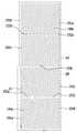
투명한 유리 또는 플라스틱 등으로 만들어진 제1 절연 기판(110) 위에 게이트선(121), 기준 전압선(131), 그리고 유지 전극(135)이 형성되어 있다. 게이트선(121)은 주로 가로 방향으로 뻗어 있으며 게이트 신호를 전달한다.A
게이트선(121)은 제1 게이트 전극(124a), 제2 게이트 전극(124b), 제3 게이트 전극(124c) 및 다른 층 또는 외부 구동 회로와의 접속을 위한 넓은 끝 부분(미도시)을 포함한다.The
기준 전압선(131)은 게이트선(121)과 평행하게 뻗을 수 있으며, 확장부(136)를 가지며, 확장부(136)는 뒤에서 설명하는 접촉 구멍(185c)을 통해 제3 드레인 전극(175c)과 연결되어 있다.The
기준 전압선(131)은 화소 영역을 둘러싸는 유지 전극(135)을 포함한다.The
게이트선(121), 기준 전압선(131), 그리고 유지 전극(135) 위에는 게이트 절연막(gate insulating layer)(140)이 형성되어 있다.A
게이트 절연막(140) 위에는 비정질 또는 결정질 규소 등으로 만들어질 수 있는 제1 반도체(154a), 제2 반도체(154b), 및 제3 반도체(154c)가 형성되어 있다.A
제1 반도체(154a), 제2 반도체(154b), 및 제3 반도체(154c) 위에는 복수의 저항성 접촉 부재(ohmic contact)(163a, 163b, 163c, 165a, 165b, 165b)가 형성되어 있다. 반도체(154a, 154b, 154c)가 산화물 반도체인 경우, 저항성 접촉 부재는 생략될 수 있다.A plurality of
저항성 접촉 부재(163a, 163b, 163c, 165a, 165b, 165b)와 게이트 절연막(140) 위에는 제1 소스 전극(173a) 및 제2 소스 전극(173b)을 포함하는 데이터선(171), 제1 드레인 전극(175a), 제2 드레인 전극(175b), 제3 소스 전극(173c) 및 제3 드레인 전극(175c)을 포함하는 데이터 도전체(171, 173a, 173b 173c, 175a, 175b, 175c)가 형성되어 있다.A
제2 드레인 전극(175b)은 제3 소스 전극(173c)과 연결되어 있고, 제3 드레인 전극(175c)은 기준 전압선(131)의 확장부(136)와 접촉 구멍(185c)를 통해 연결된다.The
제1 게이트 전극(124a), 제1 소스 전극(173a), 및 제1 드레인 전극(175a)은 제1 반도체(154a)와 함께 제1 박막 트랜지스터(Qa)를 형성하며, 박막 트랜지스터의 채널(channel)은 제1 소스 전극(173a)과 제1 드레인 전극(175a) 사이의 반도체 부분(154a)에 형성된다. 이와 유사하게, 제2 게이트 전극(124b), 제2 소스 전극(173b), 및 제2 드레인 전극(175b)은 제2 반도체(154b)와 함께 제2 박막 트랜지스터(Qb)를 형성하며, 박막 트랜지스터의 채널은 제2 소스 전극(173b)과 제2 드레인 전극(175b) 사이의 반도체 부분(154b)에 형성되고, 제3 게이트 전극(124c), 제3 소스 전극(173c), 및 제3 드레인 전극(175c)은 제3 반도체(154c)와 함께 제3 박막 트랜지스터, 즉 분압 트랜지스터(Qr)를 형성하며, 제3 박막 트랜지스터의 채널은 제3 소스 전극(173c)과 제3 드레인 전극(175c) 사이의 반도체 부분(154c)에 형성된다. 분압 스위칭 소자(Qr)는 게이트선(121)이 전달하는 게이트 신호에 따라 제어되며, 분압 스위칭 소자(Qr) 및 제2 스위칭 소자(Qb)가 턴온되면 데이터선(171)이 전달하는 데이터 전압이 제2 스위칭 소자(Qb) 및 분압 스위칭 소자(Qr)에 의해 분압되어 액정 축전기에 전달될 수 있다.The
데이터 도전체(171, 173a, 173b 173c, 175a, 175b, 175c) 및 노출된 반도체(154a, 154b, 154c) 부분 위에는 질화규소 또는 산화규소 따위의 무기 절연물로 만들어질 수 있는 제1 보호막(passivation layer)(180a)이 형성되어 있다.
제1 보호막(180a) 위에는 색필터(230)가 위치한다.A
색필터(230)가 위치하지 않는 영역 및 색필터(230)의 일부 위에는 차광 부재(light blocking member)(도시하지 않음)가 위치할 수 있다. 차광 부재는 블랙 매트릭스(black matrix)라고도 하며 빛샘을 막아준다.A light blocking member (not shown) may be positioned on a region where the
색필터(230) 위에는 덮개막(capping layer)(80)이 위치한다. 덮개막(80)은 색필터(230)가 들뜨는 것을 방지하고 색필터로부터 유입되는 용제(solvent)와 같은 유기물에 의한 액정층(3)의 오염을 억제하여 화면 구동 시 초래할 수 있는 잔상과 같은 불량을 방지한다.A
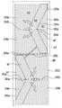
덮개막(80) 위에는 제1 부화소 전극(191a)의 제1 부영역 전극(a1)이 위치하고, 제1 부영역 전극(a1) 위에는 절연막(180b)이 위치한다.The first subregion electrode a1 of the
절연막(180b) 위에는 제1 부화소 전극(191a)의 제2 부영역 전극(a2) 및 제2 부화소 전극(191b)이 위치한다. 이때 제1 부화소 전극(191a)의 제1 부영역 전극(a1)과 제2 부영역 전극(a2)은 접촉 구멍(184a)을 통해 상호 연결될 수 있다.A second subregion electrode a2 and a
제1 부화소 전극(191a)의 제2 부영역 전극(a2)과 제2 부화소 전극(191b)은 제1 접촉 구멍(185a) 및 제2 접촉 구멍(185b)을 통해 각기 제1 드레인 전극(175a) 및 제2 드레인 전극(175b)으로부터 데이터 전압을 인가 받는다. 제1 부영역 전극(a1)과 제2 부영역 전극(a2)은 접촉 구멍(184a)을 통해 전기적으로 연결되어 있는바, 제1 부영역 전극(a1)은 제2 부영역 전극(a2)이 인가받은 데이터 전압(제1 전압)을 전달 받는다.The second sub-region electrode a2 and the second
보다 구체적으로, 본 실시예에 따른 표시 장치의 하나의 화소 영역은 제1 부화소 전극(191a), 제2 부화소 전극(191b) 및 공통 전극(270)을 포함하며, 이는 위치 상으로 구별되는 상부 단위 전극(UP)과 하부 단위 전극(DP)을 포함하며, 인가되는 전기장의 크기로 구별되는 제1 부분(R1), 제2 부분(R2) 및 제3 부분(R3)을 포함한다.More specifically, one pixel area of the display device according to the present exemplary embodiment includes a
상부 단위 전극(UP) 및 하부 단위 전극(DP)에 위치하는 제1 부화소 전극(191a)의 제1 부영역 전극(a1)은 제1 부화소 전극(191a)의 제2 부영역 전극(a2)과 상이한 층에 위치하며, 일례로써 절연막을 사이에 두고 상이한 층에 위치할 수 있다.The first subregion electrode a1 of the
제1 부영역 전극(a1)은 상부 단위 전극(UP) 및 하부 단위 전극(DP)에 위치하는 각각의 제1 부영역 전극(a1)을 연결하기 위한 제1 연결부(195a)를 더 포함할 수 있으며, 제1 연결부(195a)의 형상은 제한이 없다.The first subregion electrode a1 may further include a
제1 부영역 전극(a1)은 제1 박막 트랜지스터와 연결된 제2 부영역 전극(a2)과 전기적으로 연결되어 제1 전압을 인가받을 수 있다.The first subregion electrode a1 may be electrically connected to the second subregion electrode a2 connected to the first thin film transistor to receive a first voltage.
하나의 상부 또는 하부 단위 전극(UP, DP)에 위치하는 제2 부영역 전극(a2)은 대략적으로 하나의 밑변과 두 개의 빗변으로 이루어지는 삼각형일 수 있으며, 상기 하나의 밑변은 하나의 화소 영역의 테두리와 대응할 수 있다.The second subregion electrode a2 positioned on one upper or lower unit electrode UP and DP may be a triangle consisting of approximately one base and two hypotenuses, and the one base is a It can correspond to the border.
또한, 상부 단위 전극과 하부 단위 전극에 위치하는 제1 부화소 전극(191a)의 제2 부영역 전극(a2)은 상호 연결될 수 있으며, 일례로써 화소 영역의 테두리를 따라 연장된 제1 연결부(195a)를 통해 연결될 수 있다.In addition, the second subregion electrode a2 of the
제2 부영역 전극(a2)은 제1 박막 트랜지스터와 연결되어 제1 전압을 인가받을 수 있으며, 이는 고계조를 나타낸다.The second subregion electrode a2 is connected to the first thin film transistor to receive a first voltage, which indicates a high gradation.
제2 부화소 전극(191b)은 하나의 화소 영역 테두리와 평행하는 테두리를 포함하고, 제1 부화소 전극(191a)의 제2 부영역 전극(a2)이 포함하는 두 개의 빗변에 대해 대응하는 빗변을 포함할 수 있다. 따라서, 상부 단위 전극 또는 하부 단위 전극을 살펴보면, 제2 부화소 전극(191b)과 제1 부화소 전극(191a)의 제2 부영역 전극(a2)은 평면 상으로 상호 중첩되지 않으면서 가로 세로 길이가 유사한 사각형 형상을 나타낼 수 있다.The
또한, 상부 단위 전극(UP) 및 하부 단위 전극(DP)에 위치하는 제2 부화소 전극(191b)은 제2 연결부(195b)를 통해 전기적으로 연결될 수 있다. 일례로써 제2 연결부(195b)는 제2 부화소 영역(a2)의 제2 미세 가지부(194b)의 끝 부분에서 연장되어 상부 단위 전극(UP)과 하부 단위 전극(DP)을 연결할 수 있다.In addition, the
제2 부화소 전극(191b)은 분압 트랜지스터와 연결된 제2 박막 트랜지스터와 연결되어 제1 전압 보다 낮은 제2 전압을 인가받을 수 있다.The
이때, 제2 부영역 전극(a2)이 위치하는 영역을 제1 부분, 제1 부영역 전극(a1)과 제2 부화소 전극(191b)이 중첩하는 영역을 제2 부분, 제2 부화소 전극(191b)에서 제1 부영역 전극(a1)과 중첩하지 않는 영역을 제3 부분으로 정의한다.At this time, the region where the second subregion electrode a2 is located is a first part, the region where the first subregion electrode a1 and the
각각의 화소 전극에 인가되는 전압과 공통 전압의 차이에 따라 제1 부분(R1)에 위치하는 액정층에 가해지는 전기장의 세기가 가장 크고, 제3 부분(R3)에 위치하는 액정층에 가해지는 전기장의 세기가 가장 작다. 제2 부분(R2)에는 제1 부화소 전극(191a)의 제1 부영역 전극(a1)에 의한 전기장의 영향이 존재하기 때문에 제2 부분(R2)에 위치하는 액정층에 가해지는 전기장의 세기는 제1 부분(R1)에 위치하는 액정층에 가해지는 전기장의 세기보다는 작고, 제3 부분(R3)에 위치하는 액정층에 가해지는 전기장의 세기보다는 크게 된다.According to the difference between the voltage applied to each pixel electrode and the common voltage, the intensity of the electric field applied to the liquid crystal layer located in the first part R1 is the largest, and applied to the liquid crystal layer located in the third part R3. The intensity of the electric field is the smallest. The intensity of the electric field applied to the liquid crystal layer located in the second part R2 because the influence of the electric field by the first subregion electrode a1 of the
이처럼, 본 발명의 실시예에 따른 표시 장치는 하나의 화소 영역을 상대적으로 높은 제1 전압이 인가되는 제1 부화소 전극(191a)이 위치하는 제1 부분(R1), 제1 부화소 전극(191a)의 일부분과 상대적으로 낮은 제2 전압이 인가되는 제2 부화소 전극(191b)의 일부분이 절연막을 사이에 두고 중첩하는 제2 부분(R2), 그리고 상대적으로 낮은 제2 전압이 인가되는 제2 부화소 전극(191b)만이 위치하는 제3 부분(R3)으로 구분한다. 이에 대해서는 이하에서 도 5 내지 도 8을 참조하여 보다 상세하게 설명하기로 한다.As described above, in the display device according to the exemplary embodiment, the first portion R1 and the
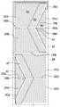
이제, 상부 표시판(200)에 대하여 설명한다.Now, the
투명한 유리 또는 플라스틱 등으로 만들어진 제2 절연 기판(210) 위에 차광 부재(220)와 공통 전극(270)이 형성되어 있다.A
그러나, 본 발명의 다른 일 실시예에 따른 액정 표시 장치의 경우, 차광 부재(220)는 하부 표시판(100) 위에 위치할 수 있고, 발명의 다른 일 실시예에 따른 액정 표시 장치의 경우, 색 필터는 상부 표시판(200)에 위치할 수도 있다.However, in the case of the liquid crystal display according to another embodiment of the present invention, the
표시판(100, 200)의 안쪽 면에는 배향막(alignment layer)(도시하지 않음)이 형성되어 있으며 이들은 수직 배향막일 수 있다.An alignment layer (not shown) is formed on the inner surfaces of the
두 표시판(100, 200)의 바깥쪽 면에는 편광자(polarizer)(도시하지 않음)가 구비되어 있는데, 두 편광자의 투과축은 직교하며 이중 한 투과축은 게이트선(121)에 대하여 나란한 것이 바람직하다. 그러나, 편광자는 두 표시판(100, 200) 중 어느 하나의 바깥쪽 면에만 배치될 수도 있다.A polarizer (not shown) is provided on the outer surfaces of the two
액정층(3)은 음의 유전율 이방성을 가지며, 액정층(3)의 액정 분자는 전기장이 없는 상태에서 그 장축이 두 표시판(100, 200)의 표면에 대하여 수직을 이루도록 배향되어 있다. 따라서 전기장이 없는 상태에서 입사광은 직교 편광자를 통과하지 못하고 차단된다.The
액정층(3)과 배향막 중 적어도 하나는 광 반응성 물질, 보다 구체적으로 반응성 메소겐(reactive mesogen)을 포함할 수 있다.At least one of the
그러면, 본 실시예에 따른 표시 장치, 일례로써 액정 표시 장치의 구동 방법에 대하여 간략하게 설명한다. 이는 도 13에서 도시하는 회로도를 참조할 수 있다.Then, a method of driving the display device according to the present embodiment, for example, a liquid crystal display device will be briefly described. This may refer to the circuit diagram shown in FIG. 13.
게이트선(121)에 게이트 온 신호가 인가되면, 제1 게이트 전극(124a), 제2 게이트 전극(124b), 그리고 제3 게이트 전극(124c)에 게이트 온 신호가 인가되어, 제1 스위칭 소자(Qa), 제2 스위칭 소자(Qb), 그리고 제3 스위칭 소자인 분압 트랜지스터(Qr)가 턴 온 된다. 이에 따라 데이터선(171)에 인가된 데이터 전압은 턴 온 된 제1 스위칭 소자(Qa) 및 제2 스위칭 소자(Qb)를 통해 각각 제1 부화소 전극(191a) 및 제2 부화소 전극(191b)에 인가된다. 이 때, 제1 부화소 전극(191a) 및 제2 부화소 전극(191b)에는 동일한 크기의 제1 전압이 인가된다. 하지만, 제2 부화소 전극(191b)에 인가된 전압은 제2 스위칭 소자(Qb)와 직렬 연결되어 있는 제3 스위칭 소자인 분압 트랜지스터(Qr)를 통해 분압되어 제2 전압이 된다. 따라서, 제2 부화소 전극(191b)에 인가되는 전압은 제1 부화소 전극(191a)에 인가되는 전압보다 더 작게 된다.When a gate-on signal is applied to the
다시, 도 2를 참고하면, 본 실시예에 따른 표시 장치의 하나의 화소 영역은 제1 부화소 전극(191a)의 제1 부영역 전극(a1)만이 위치하는 제1 부분(R1), 제1 부화소 전극(191a)의 제2 부영역 전극(a2)이 위치하며 제2 부화소 전극(191b)과 중첩하는 제2 부분(R2) 및 제2 부화소 전극(191b)의 일부분, 즉 제1 부화소 전극(191a)의 제2 부영역 전극(a2)과 중첩하지 않는 제2 부화소의 제3 부분(R3)으로 이루어진다.Again, referring to FIG. 2, one pixel area of the display device according to the present exemplary embodiment includes a first portion R1 and a first portion in which only the first sub-region electrode a1 of the
또한, 하나의 화소 영역은 하부 표시판(100)에 위치하는 상부 단위 전극(UP)과 하부 단위 전극(DP) 그리고 상부 표시판(200)에 위치하는 공통 전극(270)을 포함한다. 따라서, 각각의 상부 단위 전극과 하부 단위 전극은 각각 제1 부분(R1), 제2 부분(R2) 및 제3 부분(R3)을 포함할 수 있으며, 제1 부분(R1), 제2 부분(R2) 및 제3 부분(R3)은 각각의 상부 단위 전극 및 하부 단위 전극에서 두 개의 영역으로 구분될 수 있는바, 각 부분들은 하나의 화소 영역에서는 네 개의 영역으로 구분될 수 있다.In addition, one pixel area includes an upper unit electrode UP and a lower unit electrode DP disposed on the
또한, 도 2(a)를 살펴보면, 본 발명의 화소 영역에 대한 액정 분자의 배열을 알 수 있다. 구체적으로 한편, 상부 단위 전극에서 가로 줄기부(192a, 192b)를 기준으로 일측에 위치하는 제1 미세 가지부 및 제2 미세가지부(194a, 194b)는 제1 방향으로 기울어지게 연장된다. 이때 가로 줄기부의 일측에 위치하는 액정층의 액정 분자는 제1 방향을 따라 배열될 수 있다.Also, referring to FIG. 2(a), the arrangement of liquid crystal molecules in the pixel region of the present invention can be seen. Specifically, on the other hand, the first minute branch portions and the second
또한, 상부 단위 전극에서 가로 줄기부(192a, 192b)를 기준으로 타측에 위치하는 제1 미세 가지부 및 제2 미세 가지부(194a, 194b)는 제2 방향으로 기울어지게 연장된다. 이때 가로 줄기부의 타측에 위치하는 액정층의 액정 분자(31)는 제2 방향을 따라 배열될 수 있다.In addition, the first minute branch portions and the second
이와 마찬가지로, 하부 단위 전극에서 가로 줄기부(192a, 192b)를 기준으로 일측에 위치하는 제1 미세 가지부 및 제2 미세가지부는 제2 방향으로 기울어지게 연장된다. 이때 가로 줄기부의 일측에 위치하는 액정층(3)의 액정 분자는 제2 방향을 따라 배열될 수 있다.Likewise, the first minute branch portions and the second minute branch portions positioned at one side of the lower unit electrode with respect to the
또한, 하부 단위 전극에서 가로 줄기부(192a, 192b)를 기준으로 타측에 위치하는 제1 미세 가지부 및 제2 미세 가지부는 제1 방향으로 기울어지게 연장된다. 이때 가로 줄기부의 타측에 위치하는 액정층의 액정 분자는 제1 방향을 따라 배열될 수 있다.In addition, the first minute branch portions and the second minute branch portions positioned on the other side of the lower unit electrode with respect to the
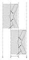
그러면 도 5 내지 도 8을 참조하여 본 발명의 일 실시예에 따른 기본 화소 전극의 형상을 구체적으로 살펴본다. 도 5는 본 발명의 일 실시예에 따른 기본 화소의 평면도이고, 도 6은 본 발명의 일 실시예에 따른 제1 부화소 전극(191a)의 제1 부영역 전극(a1)의 평면도이고, 도 7은 본 발명의 일 실시예에 따른 제1 부화소 전극(191a)의 제2 부영역 전극(a2) 및 제2 부화소 전극의 평면도이고, 도 8(a) 내지 도 8(b)는 곡면형 표시 장치를 제조함에 따른 패널의 시프트를 나타낸 것이다.Then, a shape of a basic pixel electrode according to an exemplary embodiment of the present invention will be described in detail with reference to FIGS. 5 to 8. 5 is a plan view of a basic pixel according to an embodiment of the present invention, and FIG. 6 is a plan view of a first subregion electrode a1 of the
도 5를 참고하면, 본 실시예에 따른 표시 장치의 하나의 화소 영역은 제1 부화소 전극(191a)과 제2 부화소 전극(191b)을 포함하며, 이는 위치 상으로 구별되는 상부 단위 전극(UP)과 하부 단위 전극(DP)을 포함하며, 인가되는 전기장의 크기로 구별되는 제1 부분(R1), 제2 부분(R2) 및 제3 부분(R3)으로 구분 가능하다.Referring to FIG. 5, one pixel area of the display device according to the present exemplary embodiment includes a
우선, 제1 부화소 전극(191a)과 제2 부화소 전극(191b)과 관련하여 위치 상으로 구분되는 상부 단위 전극(UP) 및 하부 단위 전극(DP)에 대해 도 5 내지 7을 참조하여 살펴본다. 하나의 상부 단위 전극(UP) 또는 하부 단위 전극(DP)은 제1 부화소 전극(191a)과 제2 부화소 전극(191b)을 포함하며, 하나의 상부 단위 전극(UP), 하부 단위 전극(DP) 및 공통 전극(270)이 하나의 화소 영역을 형성한다.First, the upper unit electrode UP and the lower unit electrode DP divided by position in relation to the
도 5를 참고하면, 상부 단위 전극(UP) 및 하부 단위 전극(DP)에 위치하는 제1 부화소 전극(191a)의 제1 부영역 전극(a1)은 제1 부화소 전극(191a)의 제2 부영역 전극(a2)과 상이한 층에 위치하며, 일례로써 절연막을 사이에 두고 상이한 층에 위치할 수 있다.Referring to FIG. 5, the first subregion electrode a1 of the
제1 부영역 전극(a1)은 제2 부영역 전극(a2)의 빗변과 평행한 빗변을 가지는 형상이며, 일례로써 도 4에 도시된 바와 같이 제2 부영역 전극(a2)과 제2 부화소 전극(191b) 사이 이격된 공간과 평면상으로 닮음이다. 다만, 제1 부영역 전극(a1)은 제2 부화소 전극(191b)과 중첩하기 위해 상기 이격된 공간 보다는 넓게 형성된다.The first subregion electrode a1 has a shape having a hypotenuse parallel to the hypotenuse of the second subregion electrode a2. As an example, as shown in FIG. 4, the second subregion electrode a2 and the second subpixel It is similar in plan view to the spaced apart between the
제1 부영역 전극(a1)은 접촉 구멍을 통해 제2 부영역 전극(a2)과 연결되며, 제2 부영역 전극(a2)에 인가되는 제1 데이터 전압을 전달받는다.The first subregion electrode a1 is connected to the second subregion electrode a2 through a contact hole, and receives a first data voltage applied to the second subregion electrode a2.
또한, 제1 부영역 전극(a1)은 상부 단위 전극 및 하부 단위 전극에 위치하는 각각의 제1 부영역 전극(a1)을 연결하기 위한 제1 연결부(195a)를 더 포함할 수 있으며, 제1 연결부(195a)의 형상은 제한이 없다.In addition, the first subregion electrode a1 may further include a
따라서, 상부 단위 전극과 하부 단위 전극은 각각 제1 부영역 전극(a1)을 포함하며, 상부 단위 전극과 하부 단위 전극에 위치하는 제1 부영역 전극(a1)은 대칭되는 위치에 배치되는 동일한 형상을 가질 수 있다.Accordingly, the upper unit electrode and the lower unit electrode each include a first subregion electrode a1, and the first subregion electrode a1 positioned at the upper unit electrode and the lower unit electrode has the same shape disposed at a symmetrical position. Can have
다음, 제1 부화소 전극의 제2 부영역 전극(a2)에 대해 살펴본다. 하나의 단위 전극(UP, DP)에 위치하는 제2 부영역 전극(a2)은 대략적으로 하나의 밑변과 두 개의 빗변으로 이루어지는 삼각형일 수 있으며, 상기 하나의 밑변은 하나의 화소 영역의 테두리와 대응할 수 있다.Next, the second subregion electrode a2 of the first subpixel electrode will be described. The second subregion electrode a2 positioned on one unit electrode UP and DP may be approximately a triangle consisting of one base and two hypotenuses, and the one base may correspond to an edge of one pixel area. I can.
상부 단위 전극(UP)에 위치하는 제1 부화소 전극(191a)의 제2 부영역 전극(a2)은 제2 부영역 전극(a2)의 중앙에 위치하는 제1 가로 줄기부(192a) 및 이로부터 연장되어 서로 다른 두 개의 방향으로 연장된 복수의 제1 미세 가지부(194a)를 포함한다. 이때 제1 가로 줄기부(192a)는 상기 하나의 밑변과 수직일 수 있다.The second subregion electrode a2 of the
하부 단위 전극(DP)에 위치하는 제2 부영역 전극(a2) 역시 동일하게 제1 가로 줄기부(192a) 및 제1 미세 가지부(194a)를 포함할 수 있으며, 하부 단위 전극과 상부 단위 전극의 전극 형상은 상호 대칭일 수 있다.The second subregion electrode a2 positioned on the lower unit electrode DP may also include a first
복수의 제1 미세 가지부(194a)는 가로 줄기부(192a)를 기준으로 약 40도 내지 약 50도 기울어질 수 있다. 복수의 제1 미세 가지부(194a)의 가장 자리에 의해 발생하는 프린지 필드에 의하여, 제1 부분(R1)에 위치하는 액정층(3)의 액정 분자(31)들은 서로 다른 두 개의 방향으로 눕게 된다. 보다 구체적으로, 액정 분자(31)들은 복수의 제1 미세 가지부(194a)가 연장된 길이 방향에 평행한 방향으로 기울어진다.The plurality of first
또한, 상부 단위 전극과 하부 단위 전극에 위치하는 제1 부화소 전극(191a)의 제2 부영역 전극(a2)은 상호 연결될 수 있으며, 일례로써 화소 영역의 테두리를 따라 연장된 제1 연결부(195a)를 통해 연결될 수 있다.In addition, the second subregion electrode a2 of the
상부 단위 전극과 하부 단위 전극에 위치하는 제1 부화소 전극(191a)의 제2 부영역 전극(a2)은 동일한 형상일 수 있으며, 동일한 위치에 위치하거나 도 4에 도시된 바와 같이 상호 대칭일 수 있다.The second subregion electrode a2 of the
다음, 제2 부화소 전극(191b)은 상부 단위 전극 및 하부 단위 전극 각각에 가로 줄기부(192b) 및 이로부터 서로 다른 두 방향으로 연장되는 제2 미세 가지부(194b)를 포함할 수 있다.Next, the
제2 부화소 전극(191b)은 하나의 화소 영역 테두리와 평행하는 테두리를 포함하고, 제1 부화소 전극(191a)의 제2 부영역 전극(a2)이 포함하는 두 개의 빗변에 대해 대응하는 빗변을 포함할 수 있다. 따라서, 상부 단위 전극 또는 하부 단위 전극을 살펴볼 때, 제2 부화소 전극(191b)과 제1 부화소 전극의 제2 부영역 전극(a2)은 평면 상으로 상호 중첩되지 않으면서 가로 세로 길이가 유사한 사각형 형상을 나타낼 수 있다. 이러한 상부 단위 전극 또는 하부 단위 전극을 세로 방향으로 합쳐놓은 경우, 세로 방향 길이가 가로 방향 길이보다 긴 하나의 화소 영역을 형성한다.The
복수의 제2 미세 가지부(194b)는 가로 줄기부(192b)를 기준으로 약 40도 내지 약 50도 기울어질 수 있다. 복수의 제2 미세 가지부(194b)의 가장 자리에 의해 발생하는 프린지 필드에 의하여, 제3 부분(R3)에 위치하는 액정층(3)의 액정 분자(31)들은 서로 다른 두 개의 방향으로 눕게 된다. 보다 구체적으로, 액정 분자(31)들은 복수의 제2 미세 가지부(194b)가 연장된 길이 방향에 평행한 방향으로 기울어진다.The plurality of second
또한, 제1 미세 가지부(194a) 및 제2 미세 가지부(194b)는 동일한 기울기를 가질 수 있다. 구체적으로 각각의 가로 줄기부에 대해 동일한 측면에 위치하는 제1 미세 가지부(194a) 및 제2 미세 가지부(194b)는 동일한 기울기를 가지면서 연장된다. 따라서, 상이한 전압이 인가되는 경우에도, 동일한 측면에 위치하는 액정 분자(31)들은 동일한 방향으로 배열될 수 있다.In addition, the
또한, 상부 단위 전극 및 하부 단위 전극에 위치하는 제2 부화소 전극(191b)은 제2 연결부(195b)를 통해 전기적으로 연결될 수 있다. 일례로써 제2 연결부(195b)는 상기 제2 부화소 영역의 제2 미세 가지부(194b)의 끝 부분에서 연장되어 상기 상부 단위 전극과 상기 하부 단위 전극을 연결할 수 있다.In addition, the
다음, 인가되는 전기장의 크기에 따라 구분되는 제1 부분(R1), 제2 부분(R2) 및 제3 부분(R3)에 대해 살펴본다.Next, the first portion R1, the second portion R2, and the third portion R3 divided according to the magnitude of the applied electric field will be described.
우선, 제1 부분(R1)은 하부 표시판에 위치하는 제1 부화소 전극(191a)의 제2 부영역 전극(a2)과 상부 표시판(200)에 위치하는 공통 전극(270)이 전기장을 생성한다. 이때 제2 부영역 전극(a2)에 인가되는 전압은 한 화소 영역에 인가되는 전압 중 가장 큰 값을 가지는바, 공통 전극(270)과 전기장의 세기가 센 영역을 형성한다.First, in the first portion R1, an electric field is generated by the second subregion electrode a2 of the
다음, 제2 부분(R2)은 제1 부화소 전극(191a)의 제1 부영역 전극(a1)과 제2 부화소 전극(191b)이 중첩되는 영역이다. 제1 부영역 전극(a1)과 상부 표시판의 공통 전극 사이에 형성되는 전기장과 함께, 제2 부화소 전극(191b)의 제2 미세 가지부와 공통 전극 사이에 형성되는 전기장에 의해 액정층(3)의 액정 분자(31)가 배열된다. 이때 제2 부분(R2)에는 제1 부화소 전극(191a)의 제1 부영역 전극(a1)에 의한 전기장의 영향 및 제2 부화소 전극(191b)에 의한 전기장의 영향이 공존하는바, 제2 부분(R2)에 위치하는 액정층에 가해지는 전기장의 세기는 제1 부분(R1)에위치하는 액정층에 가해지는 전기장의 세기보다는 작고, 제3 부분(R3)에 위치하는 액정층에 가해지는 전기장의 세기보다는 크게 된다.Next, the second portion R2 is a region where the first subregion electrode a1 and the
다시, 도 6을 참고하면, 제3 부분(R3)은 하부 표시판(100)의 제2 부화소 전극(191b)과 상부 표시판(200)의 공통 전극이 함께 전기장을 생성한다. 이때 제2 부화소 전극(191b)에 인가되는 전압은 제2 스위칭 소자를 통해 인가되는 제2 전압으로서, 분압 트랜지스터에 의해 제1 전압보다 낮은 전압이 인가된다. 따라서, 제2 부화소 전극(191b)과 공통 전극 사이에 형성되는 전기장은 제1 부화소 전극(191a)의 제2 부영역 전극(a2)과 공통 전극 사이에 형성되는 전기장보다 작다.Again, referring to FIG. 6, in the third portion R3, the
따라서, 제1 부분(R1)에 위치하는 액정층에 가해지는 전기장의 세기가 가장 크고, 제3 부분(R3)에 위치하는 액정층에 가해지는 전기장의 세기가 가장 작다. 제2 부분(R2)에는 제1 부화소 전극(191a)의 제1 부영역 전극(a1)에 의한 전기장의 영향이 존재하기 때문에 제2 부분(R2)에 위치하는 액정층에 가해지는 전기장의 세기는 제1 부분(R1)에 위치하는 액정층에 가해지는 전기장의 세기보다는 작고, 제3 부분(R3)에 위치하는 액정층에 가해지는 전기장의 세기보다는 크게 된다.Accordingly, the strength of the electric field applied to the liquid crystal layer positioned in the first portion R1 is the largest, and the strength of the electric field applied to the liquid crystal layer positioned in the third portion R3 is the lowest. The intensity of the electric field applied to the liquid crystal layer located in the second part R2 because the influence of the electric field by the first subregion electrode a1 of the
이처럼, 본 발명의 실시예에 따른 표시 장치는 하나의 화소 영역을 상대적으로 높은 제1 전압이 인가되는 제1 부화소 전극(191a)이 위치하는 제1 부분(R1), 제1 부화소 전극(191a)의 일부분과 상대적으로 낮은 제2 전압이 인가되는 제2 부화소 전극(191b)의 일부분이 절연막을 사이에 두고 중첩하는 제2 부분(R2), 그리고 상대적으로 낮은 제2 전압이 인가되는 제2 부화소 전극(191b)만이 위치하는 제3 부분(R3)으로 구분한다.As described above, in the display device according to the exemplary embodiment, the first portion R1 and the
따라서, 제1 부분(R1), 제2 부분(R2), 제3 부분(R3)에 대응하는 액정 분자들에 가해지는 전기장의 세기가 다르게 되어, 액정 분자들이 기울어지는 각도가 다르게 되고, 이에 따라 각 부분의 휘도가 달라진다. 이처럼, 하나의 화소 영역을 서로 다른 휘도를 가지는 3개의 부분으로 구분하게 되면, 계조에 따른 투과율의 변화를 완만하게 조절함으로써, 측면에서 저계조와 고계조에서도 계조 변화에 따라 투과율이 급격히 변화하는 것을 방지함으로써, 정측면 시인성을 정면 시인성에 가깝게 하면서도, 저계조와 고계조에서도 정확한 계조 표현이 가능하다.Accordingly, the strength of the electric field applied to the liquid crystal molecules corresponding to the first part R1, the second part R2, and the third part R3 is different, so that the angle at which the liquid crystal molecules are inclined is different. The luminance of each part is different. In this way, when one pixel area is divided into three parts having different luminance, the change in transmittance according to the gradation is gently adjusted, so that the transmittance changes rapidly according to the gradation change even in low and high gradations from the side. By preventing it, it is possible to accurately express gradations even in low and high gradations while bringing the front visibility closer to the front visibility.
한편, 상부 단위 전극에서 가로 줄기부(192a, 192b)를 기준으로 일측에 위치하는 제1 미세 가지부 및 제2 미세가지부(194a, 194b)는 제1 방향으로 기울어지게 연장된다. 이때 가로 줄기부의 일측에 위치하는 액정층의 액정 분자는 제1 방향을 따라 배열될 수 있다.Meanwhile, the first and
또한, 상부 단위 전극에서 가로 줄기부(192a, 192b)를 기준으로 타측에 위치하는 제1 미세 가지부 및 제2 미세 가지부(194a, 194b)는 제2 방향으로 기울어지게 연장된다. 이때 가로 줄기부의 타측에 위치하는 액정층의 액정 분자(31)는 제2 방향을 따라 배열될 수 있다.In addition, the first minute branch portions and the second
이와 마찬가지로, 하부 단위 전극에서 가로 줄기부(192a, 192b)를 기준으로 일측에 위치하는 제1 미세 가지부 및 제2 미세가지부는 제2 방향으로 기울어지게 연장된다. 이때 가로 줄기부의 일측에 위치하는 액정층(3)의 액정 분자는 제2 방향을 따라 배열될 수 있다.Likewise, the first minute branch portions and the second minute branch portions positioned at one side of the lower unit electrode with respect to the
또한, 하부 단위 전극에서 가로 줄기부(192a, 192b)를 기준으로 타측에 위치하는 제1 미세 가지부 및 제2 미세 가지부는 제1 방향으로 기울어지게 연장된다. 이때 가로 줄기부의 타측에 위치하는 액정층의 액정 분자는 제1 방향을 따라 배열될 수 있다.In addition, the first minute branch portions and the second minute branch portions positioned on the other side of the lower unit electrode with respect to the
도 8(a)을 참조하면, 곡면형 표시 장치를 제공함에 있어 표시판에 힘을 가하는 경우, 상부 표시판(200)과 하부 표시판(100)의 얼라인이 좌우로 어긋날 수 있다.Referring to FIG. 8A, when a force is applied to the display panel in providing the curved display device, the alignment of the
이때 본 발명의 일 실시예에 따르면, 가로 줄기부(192a, 192b)를 기준으로 일측에 위치하는 제1 미세 가지부 및 제2 미세 가지부는 동일한 방향으로 기울어지게 연장되어 이에 의한 액정 분자 역시 동일한 방향으로 배열된다.At this time, according to an embodiment of the present invention, the first and second minute branches positioned on one side of the
또한, 가로 줄기부(192a, 192b)를 기준으로 타측에 위치하는 제1 미세 가지부 및 제2 미세 가지부 역시 동일한 방향으로 기울어지게 연장되어 이에 의한 액정 분자(31)는 동일한 제2 방향으로 배열된다.In addition, the first minute branches and the second minute branches located on the other side with respect to the
따라서, 가로 줄기부(192a, 192b)를 기준으로 상하측에 위치하는 미세 가지부는 인가되는 전압에 관계없이 동일한 액정 분자 배열을 나타낸다. 도 8(b)에 도시된 바와 같이 상부 표시판(200) 또는 하부 표시판(100)이 좌우로 미스-얼라인 된 경우에도, 상하부 전극 사이에는 동일하게 배열된 액정 분자가 위치하는바, 텍스쳐의 발현을 감소시킬 수 있다.Accordingly, the minute branches positioned on the upper and lower sides of the
도 9 내지 도 10을 참조하여 본 발명의 다른 실시예에 따른 기본 화소 전극의 평면도를 살펴본다. 도 9는 본 발명의 다른 실시예에 따른 기본 화소의 평면도이고, 도 10은 본 발명의 다른 실시예에 따른 기본 화소의 평면도이다. 전술한 본 발명의 일 실시예와 동일 유사한 구성요소에 대한 설명은 생략한다.A plan view of a basic pixel electrode according to another exemplary embodiment of the present invention will be described with reference to FIGS. 9 to 10. 9 is a plan view of a basic pixel according to another exemplary embodiment of the present invention, and FIG. 10 is a plan view of a basic pixel according to another exemplary embodiment of the present invention. Description of the same and similar components as in the above-described embodiment of the present invention will be omitted.
도 9를 참조하면, 상부 단위 전극 및 하부 단위 전극에 위치하는 제1 부화소 전극(191a)의 제1 부영역 전극(a1)을 연결하는 제1 연결부(195a)는 화소 영역이 포함하는 가로 줄기부(192a, 192b)와 평행할 수 있다.Referring to FIG. 9, a
또한, 이와 더불어 제2 부화소 전극(191b)이 포함하는 제2 가로 줄기부(192b)의 일부 영역이 제거된다. 구체적으로, 제2 부화소 전극(191b)과 제1 부화소 전극(191a)의 제1 부영역 전극(a1)은 중첩하는데, 이때 제1 부영역 전극(a1)과 중첩하는 제2 가로 줄기부에 해당하는 영역이 제거된다.In addition, a partial region of the second
따라서, 제1 전압을 인가 받는 제1 부화소 전극(191a)의 제2 부영역 전극(a2)과, 제2 부영역 전극(a2)과 전기적으로 연결되어 있으며 제2 부화소 전극(191b)의 제2 가로 줄기부가 삭제되어 제2 부화소 전극(191b)과 중첩하지 않는 제1 부화소 전극(191a)의 제1 부영역 전극(a1)의 일부는 공통 전극(270)과 전기장을 생성하는 제1 부분(R1)을 이룬다.Therefore, the second sub-region electrode a2 of the
또한, 제1 부영역 전극(a1)과 중첩하지 않으면서 제2 전압을 인가받는 제2 부화소 전극(191b)의 일부는 상부 표시판에 위치하는 공통 전극(270)과 전기장을 생성하는 제3 부분(R3)을 이룬다.In addition, a part of the
마지막으로, 제1 부영역 전극(a1)과 중첩하는 복수의 제2 미세 가지부가 공통 전극(270)과 전기장을 생성하며, 이와 더불어 제1 부영역 전극(a1)은 공통 전극(270)과 전기장을 생성하며, 해당 영역은 제2 부분(R2)을 이룬다.Finally, a plurality of second minute branches overlapping the first subregion electrode a1 generate an electric field with the
이때 전기장의 세기는 전술한 바와 같이 제1 부분(R1), 제2 부분(R2), 제3 부분(R3) 순으로 작아진다.At this time, the strength of the electric field decreases in the order of the first portion R1, the second portion R2, and the third portion R3, as described above.
이와 같은 다른 실시예에 따르면, 본 발명의 일 실시예와 비교하여 제2 가로 줄기부가 제거된 영역 및 제2 연결부가 위치하는 영역에서의 텍스쳐 발현이 감소된다.According to such another embodiment, the expression of texture in the region where the second horizontal stem portion is removed and the region where the second connection portion is located is reduced compared to the exemplary embodiment of the present invention.
다음, 도 10을 참조하여 본 발명의 다른 실시예를 살펴본다. 도 10에 도시된 바와 같이 상부 단위 전극 및 하부 단위 전극에 위치하는 각각의 제1 부영역 전극(a1)을 연결하는 연결부가 없으며, 각각의 제1 부영역 전극(a1)은 제2 부영역 전극(a2)과 전기적으로 연결되는 접촉 구멍(184a)을 통해 전압을 인가 받는다.Next, another embodiment of the present invention will be described with reference to FIG. 10. As shown in FIG. 10, there is no connection part connecting each of the first subregion electrodes a1 positioned on the upper unit electrode and the lower unit electrode, and each first subregion electrode a1 is a second subregion electrode. A voltage is applied through the
또한, 도 9와 마찬가지로 제2 부화소 전극(191b)이 포함하는 제2 가로 줄기부의 일부 영역이 제거된다. 구체적으로, 제2 부화소 전극(191b)과 제1 부화소 전극(191a)의 제1 부영역 전극(a1)은 중첩하는데, 제1 부영역 전극(a1)과 중첩하는 제2 가로 줄기부에 해당하는 영역이 제거된다.Also, as in FIG. 9, a partial area of the second horizontal stem included in the
따라서, 제1 전압을 인가받는 제1 부화소 전극(191a)의 제2 부영역 전극(a2)과, 제2 부영역 전극(a2)과 전기적으로 연결되어 있으며 제2 부화소 전극(191b)의 제2 가로 줄기부가 삭제되어 제2 부화소 전극(191b)과 중첩하지 않는 제1 부화소 전극(191a)의 제1 부영역 전극(a1) 일부는 공통 전극(270)과 전기장을 생성하는 제1 부분(R1)을 이룬다.Therefore, the second sub-region electrode a2 of the
또한, 제1 부영역 전극(a1)과 중첩하지 않으면서 제2 전압을 인가받는 제2 부화소 전극(191b)의 일부는 상부 표시판에 위치하는 공통 전극(270)과 전기장을 생성하는 제3 부분(R3)을 이룬다.In addition, a part of the
마지막으로, 제1 부영역 전극(a1)과 중첩하는 복수의 제2 미세 가지부(194b)가 공통 전극(270)과 전기장을 생성하며, 이와 더불어 제1 부영역 전극(a1)은 공통 전극(270)과 전기장을 생성하고, 상기 영역은 제2 부분(R2)을 이룬다.Lastly, the plurality of second
전기장의 세기는 전술한 바와 같이 제1 부분(R1), 제2 부분(R2), 제3 부분(R3) 순으로 작아진다. 이와 같은 실시예에 따르면 제1 부영역 전극을 연결하는 제1 연결부에 의해 발생하는 텍스쳐의 발현을 감소시킬 수 있다.As described above, the strength of the electric field decreases in the order of the first portion R1, the second portion R2, and the third portion R3. According to such an embodiment, it is possible to reduce the expression of texture generated by the first connector connecting the first subregion electrode.
이하에서 도 11 내지 도 13을 참조하여 본 발명의 일 실시예에 따른 표시 장치에 대해 살펴본다. 도 11(a) 내지 도 11(c)는 본 발명의 실시예에 따른 화소 영역의 이미지이고, 도 12는 본 발명의 일 실시예에 따른 투과율 및 시인성에 대한 그래프이며, 도 13은 본 발명의 실시예에서 계조에 대한 투과율을 나타내는 그래프이다.Hereinafter, a display device according to an exemplary embodiment will be described with reference to FIGS. 11 to 13. 11(a) to 11(c) are images of a pixel area according to an embodiment of the present invention, FIG. 12 is a graph of transmittance and visibility according to an embodiment of the present invention, and FIG. 13 is This is a graph showing the transmittance with respect to gradations in Examples.
도 11(a)는 본 발명의 일 실시예에 따른 하나의 화소 영역에 대한 이미지이고, 도 11(b)는 도 9에 도시된 실시예에 따른 화소 영역에 대한 이미지고, 도 11(c)는 도 10에 도시된 실시예에 따른 화소 영역에 대한 이미지이다.FIG. 11(a) is an image of one pixel area according to an embodiment of the present invention, and FIG. 11(b) is an image of a pixel area according to the embodiment shown in FIG. 9, and FIG. 11(c) Is an image of a pixel area according to the exemplary embodiment illustrated in FIG. 10.
도 11(a)를 살펴보면, 상부 단위 전극과 하부 단위 전극 사이에 위치하는 제1 부영역 전극(a1)을 연결하는 제1 연결부에 의한 텍스쳐 및 제1 부영역 전극(a1)과 제2 부화소 전극(191b)의 가로 줄기부가 중첩하는 영영역에 발생하는 텍스쳐를 제외하고는 텍스쳐의 발생이 거의 없음을 알 수 있다.Referring to FIG. 11(a), the texture by the first connector connecting the first subregion electrode a1 positioned between the upper unit electrode and the lower unit electrode, and the first subregion electrode a1 and the second subpixel It can be seen that texture is hardly generated except for the texture generated in the zero region where the horizontal stem portion of the
도 11(b)를 살펴보면, 가로 줄기부와 평행하게 형성된 제1 연결부에 의해 텍스쳐가 일부 발현되었으나, 제1 부영역 전극(a1)과 중첩하는 제2 부화소 전극(191b)의 제2 가로 줄기부를 일부 제거함에 따라 해당 영역에 발생하는 텍스쳐를 제거함을 확인하였다.Referring to FIG. 11(b), the texture was partially expressed by the first connector formed parallel to the horizontal stem, but the second horizontal stem of the
또한, 도 11(c)를 살펴보면, 도 9에 대해 제1 연결부를 삭제한 실시예인바, 제1 연결부에 의해 발생하는 텍스쳐도 제거됨을 확인하였다.In addition, referring to FIG. 11(c), it was confirmed that the texture generated by the first connector was also removed since it was an embodiment in which the first connector was deleted from FIG. 9.
도 12를 참조하면, 제일 우측에 표시된 구조는 본 발명의 비교예로서 약 0.18의 측면 시인성 지표과 약 90%의 투과율을 나타낸다. 그러나 본 발명의 일 실시예에 대해 투과율과 측면 시인성을 살펴본 경과, 투과율은 전압비가 증가함에 따라 증가하는 경향을 보이고, 측면 시인성은 전압비가 감소함에 따라 향상되는 경향을 나타냈다. 투과율과 측면 시인성은 다소 트레이드-오프 특성을 나타내는바, 이를 적절히 선택한 본 발명의 일 실시예에 따른 표시 장치는 기존 비교예에 대해 거의 동일한 투과율 대비 상당히 개선된 측면 시인성을 나타냄을 확인하였다.Referring to FIG. 12, the structure shown on the right-most side is a comparative example of the present invention, indicating a side visibility index of about 0.18 and a transmittance of about 90%. However, after examining the transmittance and side visibility for an embodiment of the present invention, the transmittance tends to increase as the voltage ratio increases, and the side visibility tends to improve as the voltage ratio decreases. Transmittance and side visibility exhibit somewhat trade-off characteristics, and it was confirmed that the display device according to the exemplary embodiment of the present invention, which is appropriately selected, exhibits considerably improved side visibility compared to the conventional comparative example.
또한, 도 13에 도시된 바와 같이 이상적인 감마 곡선에 대해 본 발명의 일 실시예에 따른 표시 장치는 저계조에서는 다소 낮은 투과율을 나타냈으나, 고계조로 갈수록 비교예에 비해 높은 투과율을 나타냄을 확인할 수 있었다.In addition, as shown in FIG. 13, it was confirmed that the display device according to the exemplary embodiment of the present invention exhibited a slightly lower transmittance in low grayscales with respect to the ideal gamma curve, but the higher the transmittance compared to the comparative example as the grayscale became higher. Could
따라서, 본 발명의 일 실시예에 따른 표시 장치는 높은 투과율 대비 상당히 개선된 측면 시인성을 나타내며, 특히 곡면형 표시 장치를 제공함에 있어서 텍스쳐의 발현을 상당히 감소시킬 수 있다.Accordingly, the display device according to an exemplary embodiment of the present invention exhibits considerably improved side visibility compared to high transmittance, and particularly, when providing a curved display device, it is possible to significantly reduce the expression of texture.
이하에서는 도 14 내지 도 18을 참조하여 본 발명의 실시예에 따른 표시 장치의 회로도를 살펴본다.Hereinafter, a circuit diagram of a display device according to an exemplary embodiment will be described with reference to FIGS. 14 to 18.
우선 도 14에 도시한 화소(PX)의 동작에 대해 설명하면, 먼저 게이트선(121)에 게이트 온 전압(Von)이 인가되면 이에 연결된 제1 스위칭 소자(Qa), 제2 스위칭 소자(Qb), 그리고 제3 스위칭 소자(Qc)가 턴 온 된다. 이에 따라 데이터선(171)에 인가된 데이터 전압은 턴 온 된 제1 스위칭 소자(Qa) 및 제2 스위칭 소자(Qb)를 통해 각각 제1 액정 축전기(Clca) 및 제2 액정 축전기(Clcb)에 인가되어 제1 액정 축전기(Clca) 및 제2 액정 축전기(Clcb)는 데이터 전압 및 공통 전압(Vcom)의 차이만큼 충전된다. 이 때, 제1 액정 축전기(Clca) 및 제2 액정 축전기(Clcb)에는 제1 및 제2 스위칭 소자(Qa, Qb)를 통해 동일한 데이터 전압이 전달되나 제2 액정 축전기(Clcb)의 충전 전압은 제3 스위칭 소자(Qc)를 통해 분압이 된다. 따라서, 제2 액정 축전기(Clcb)의 충전 전압은 제1 액정 축전기(Clca)의 충전 전압보다 작아지므로 두 부화소(PXa, PXb)의 휘도가 달라질 수 있다. 따라서, 제1 액정 축전기(Clca)에 충전되는 전압과 제2 액정 축전기(Clcb)의 충전되는 전압을 적절히 조절하면 측면에서 바라보는 영상이 정면에서 바라보는 영상에 최대한 가깝게 되도록 할 수 있고, 이에 따라 측면 시인성을 개선할 수 있다.First, the operation of the pixel PX illustrated in FIG. 14 will be described. First, when a gate-on voltage Von is applied to the
그러나 본 발명이 실시예에 따른 액정 표시 장치의 화소(PX)의 구조는 도 14에 도시한 실시예에 한정되는 것은 아니고 다양할 수 있다.However, the structure of the pixel PX of the liquid crystal display according to the exemplary embodiment of the present invention is not limited to the exemplary embodiment illustrated in FIG. 14 and may be various.
이하에서는 도 15의 실시예를 살펴본다.Hereinafter, the embodiment of FIG. 15 will be described.
본 발명의 실시예에 의한 액정 표시 장치는 복수의 게이트선(GL)과 복수의 데이터선(DL), 복수의 유지 전극선(SL)을 포함하는 신호선과 이에 연결되어 있는 복수의 화소(PX)를 포함한다. 각 화소(PX)는 한 쌍의 제1 및 제2 부화소(PXa, PXb)를 포함하고, 제1 부화소(PXa)에는 제1 부화소 전극이 형성되고, 제2 부화소(PXb)에는 제2 부화소 전극이 형성된다.The liquid crystal display according to the exemplary embodiment of the present invention includes a signal line including a plurality of gate lines GL, a plurality of data lines DL, and a plurality of storage electrode lines SL, and a plurality of pixels PX connected thereto. Include. Each pixel PX includes a pair of first and second subpixels PXa and PXb, a first subpixel electrode is formed in the first subpixel PXa, and the second subpixel PXb is A second subpixel electrode is formed.
본 발명의 실시예에 의한 액정 표시 장치는 게이트선(GL) 및 데이터선(DL)에 연결되어 있는 스위칭 소자(Q), 스위칭 소자(Q)와 연결되어 제1 부화소(PXa)에 형성되는 제1 액정 축전기(Clca)와 제1 유지 축전기(Csta), 스위칭 소자(Q)와 연결되어 제2 부화소(PXb)에 형성되는 제2 액정 축전기(Clcb)와 제2 유지 축전기(Cstb), 및 스위칭 소자(Q) 및 제2 액정 축전기(Clcb) 사이에 형성되는 보조 축전기(Cas)를 더 포함한다.The liquid crystal display according to the exemplary embodiment of the present invention includes a switching element Q connected to the gate line GL and the data line DL, and formed in the first subpixel PXa by being connected to the switching element Q. A second liquid crystal capacitor Clcb and a second storage capacitor Cstb connected to the first liquid crystal capacitor Clca and the first storage capacitor Csta, and formed in the second subpixel PXb by being connected to the switching element Q, And an auxiliary capacitor Cas formed between the switching element Q and the second liquid crystal capacitor Clcb.
스위칭 소자(Q)는 하부 표시판(100)에 구비되어 있는 박막 트랜지스터 등의 삼단자 소자로서, 그 제어 단자는 게이트선(GL)과 연결되어 있고, 입력 단자는 데이터선(DL)과 연결되어 있으며, 출력 단자는 제1 액정 축전기(Clca), 제1 유지 축전기(Csta), 보조 축전기(Cas)와 연결되어 있다.The switching element Q is a three-terminal element such as a thin film transistor provided on the
보조 축전기(Cas)의 일측 단자는 스위칭 소자(Q)의 출력 단자에 연결되고, 타측 단자는 제2 액정 축전기(Clcb) 및 제2 유지 축전기(Cstb)에 연결된다.One terminal of the auxiliary capacitor Cas is connected to the output terminal of the switching element Q, and the other terminal is connected to the second liquid crystal capacitor Clcb and the second storage capacitor Cstb.
보조 축전기(Cas)에 의해 제2 액정 축전기(Clcb)의 충전 전압이 제1 액정 축전기(Clca)의 충전 전압보다 낮게 하여 액정 표시 장치의 측면 시인성을 향상시킬 수 있다.The charging voltage of the second liquid crystal capacitor Clcb is lower than the charging voltage of the first liquid crystal capacitor Clca by the auxiliary capacitor Cas, so that side visibility of the liquid crystal display may be improved.
이하에서는 도 16의 실시예를 살펴본다.Hereinafter, the embodiment of FIG. 16 will be described.
본 발명의 실시예에 의한 액정 표시 장치는 복수의 게이트선(GLn, GLn+1), 복수의 데이터선(DL), 복수의 유지 전극선(SL)을 포함하는 신호선과 이에 연결되어 있는 복수의 화소(PX)를 포함한다. 각 화소(PX)는 한 쌍의 제1 및 제2 부화소(PXa, PXb)를 포함하고, 제1 부화소(PXa)에는 제1 부화소 전극이 형성되고, 제2 부화소(PXb)에는 제2 부화소 전극이 형성된다.A liquid crystal display according to an exemplary embodiment of the present invention includes a signal line including a plurality of gate lines GLn and GLn+1, a plurality of data lines DL, and a plurality of storage electrode lines SL, and a plurality of pixels connected thereto. (PX) is included. Each pixel PX includes a pair of first and second subpixels PXa and PXb, a first subpixel electrode is formed in the first subpixel PXa, and the second subpixel PXb is A second subpixel electrode is formed.
본 발명의 실시예에 의한 액정 표시 장치는 게이트선(GLn) 및 데이터선(DL)에 연결되어 있는 제1 스위칭 소자(Qa)와 제2 스위칭 소자(Qb), 제1 스위칭 소자(Qa)와 연결되어 제1 부화소(PX)에 형성되는 제1 액정 축전기(Clca)와 제1 유지 축전기(Csta), 제2 스위칭 소자(Qb)와 연결되어 제2 부화소에 형성되는 제2 액정 축전기(Clcb)와 제2 유지 축전기(Cstb), 제2 스위칭 소자(Qb)와 연결되고 다음 단의 게이트선(GLn+1)에 의해 스위칭되는 제3 스위칭 소자(Qc), 및 제3 스위칭 소자(Qc)와 연결되어 있는 보조 축전기(Cas)를 더 포함한다.The liquid crystal display according to the exemplary embodiment of the present invention includes a first switching element Qa, a second switching element Qb, and a first switching element Qa connected to the gate line GLn and the data line DL. A first liquid crystal capacitor Clca connected to and formed in the first subpixel PX, a first storage capacitor Csta, and a second liquid crystal capacitor connected to the second switching element Qb and formed in the second subpixel ( Clcb), the second storage capacitor Cstb, the third switching element Qc connected to the second switching element Qb and switched by the gate
제1 스위칭 소자(Qa) 및 제2 스위칭 소자(Qb)는 하부 표시판(100)에 구비되어 있는 박막 트랜지스터 등의 삼단자 소자로서, 그 제어 단자는 게이트선(GLn)과 연결되어 있고, 입력 단자는 데이터선(DL)과 연결되어 있으며, 출력 단자는 각각 제1 액정 축전기(Clca) 및 제1 유지 축전기(Csta), 제2 액정 축전기(Clcb) 및 제2 유지 축전기(Cstb)와 각각 연결되어 있다.The first switching element Qa and the second switching element Qb are three-terminal elements such as a thin film transistor provided on the
제3 스위칭 소자(Qc) 역시 하부 표시판(100)에 구비되어 있는 박막 트랜지스터 등의 삼단자 소자로서, 제어 단자는 다음 단의 게이트선(GLn+1)과 연결되어 있고, 입력 단자는 제2 액정 축전기(Clcb)와 연결되어 있으며, 출력 단자는 보조 축전기(Cas)와 연결되어 있다.The third switching element Qc is also a three-terminal element such as a thin film transistor provided on the
보조 축전기(Cas)의 일측 단자는 제3 스위칭 소자(Qc)의 출력 단자에 연결되고, 타측 단자는 유지 전극선(SL) 에 연결된다.One terminal of the auxiliary capacitor Cas is connected to the output terminal of the third switching element Qc, and the other terminal is connected to the storage electrode line SL.
본 발명의 실시예에 의한 액정 표시 장치의 동작을 살펴보면, 게이트선(GLn)에 게이트 온 전압이 인가되면 이에 연결된 제1 스위칭 소자 및 제2 스위칭 소자(Qa, Qb)가 턴 온 되고, 데이터선(171)의 데이터 전압이 제1 및 제2 부화소 전극에 인가된다.Looking at the operation of the liquid crystal display according to the exemplary embodiment of the present invention, when a gate-on voltage is applied to the gate line GLn, the first and second switching elements Qa and Qb connected thereto are turned on, and the data line A data voltage of 171 is applied to the first and second subpixel electrodes.
이어, 게이트선(GLn)에 게이트 오프 전압이 인가되고, 다음 단의 게이트선(GLn+1)에 게이트 온 전압이 인가되면 제1 및 제2 스위칭 소자(Qa, Qb)는 턴 오프되고 제3 스위칭 소자(Qc)는 턴 온된다. 이에 따라 제2 스위칭 소자(Qb)의 출력 단자와 연결된 제2 부화소 전극의 전하가 보조 축전기(Cas)로 흘러 들어 제2 액정 축전기(Clcb)의 전압이 하강한다.Subsequently, when a gate-off voltage is applied to the gate line GLn and a gate-on voltage is applied to the next gate
이와 같이 제1 및 제2 액정 축전기(Clca, Clcb)의 충전 전압을 다르게 하여 액정 표시 장치의 측면 시인성을 향상시킬 수 있다.In this way, the side visibility of the liquid crystal display may be improved by varying the charging voltages of the first and second liquid crystal capacitors Clca and Clcb.
이하에서는 도 17의 실시예를 살펴본다.Hereinafter, an embodiment of FIG. 17 will be described.
본 발명의 실시예에 의한 액정 표시 장치는 복수의 게이트선(GL), 복수의 데이터선(DL1, DL2), 복수의 유지 전극선(SL)을 포함하는 신호선과 이에 연결되어 있는 복수의 화소(PX)를 포함한다. 각 화소(PX)는 한 쌍의 제1 및 제2 액정 축전기(Clca, Clab)와 제1 및 제2 유지 축전기(Csta, Cstb)를 포함한다.The liquid crystal display according to the exemplary embodiment of the present invention includes a signal line including a plurality of gate lines GL, a plurality of data lines DL1 and DL2, and a plurality of storage electrode lines SL, and a plurality of pixels PX connected thereto. ). Each pixel PX includes a pair of first and second liquid crystal capacitors Clca and Clab and first and second storage capacitors Csta and Cstb.
각 부화소는 하나의 액정 축전기와 유지 축전기를 포함하며, 추가적으로 하나의 박막 트랜지스터(Q)를 포함한다. 하나의 화소에 속하는 두 부화소의 박막 트랜지스터(Q)는 동일한 게이트선(GL)에 연결되어 있지만, 서로 다른 데이터선(DL1, DL2)에 연결되어 있다. 서로 다른 데이터선(DL1, DL2)은 서로 다른 레벨의 데이터 전압을 동시에 인가하여 두 부화소의 제1 및 제2 액정 축전기(Clca, Clcb)가 서로 다른 충전 전압을 가지도록 한다. 그 결과 액정 표시 장치의 측면 시인성을 향상시킬 수 있다.Each subpixel includes one liquid crystal capacitor and one storage capacitor, and additionally includes one thin film transistor Q. The thin film transistors Q of the two subpixels belonging to one pixel are connected to the same gate line GL, but are connected to different data lines DL1 and DL2. Different data lines DL1 and DL2 simultaneously apply data voltages of different levels so that the first and second liquid crystal capacitors Clca and Clcb of the two subpixels have different charging voltages. As a result, side visibility of the liquid crystal display can be improved.
이하에서는 도 18의 실시예를 살펴본다.Hereinafter, the embodiment of FIG. 18 will be described.
본 발명의 일 실시예에 따른 액정 표시 장치는 도 27에 도시된 바와 같이 게이트선(GL), 데이터선(DL), 제1 전원선(SL1), 제2 전원선(SL2), 게이트선(GL) 및 데이터선(DL)에 연결되는 제1 스위칭 소자(Qa), 제2 스위칭 소자(Qb)를 포함한다.In the liquid crystal display according to an exemplary embodiment of the present invention, as illustrated in FIG. 27, a gate line GL, a data line DL, a first power line SL1, a second power line SL2, and a gate line And a first switching element Qa and a second switching element Qb connected to the GL and the data line DL.
본 발명의 일 실시예에 따른 액정 표시 장치는 제1 스위칭 소자(Qa)에 연결되는 보조 승압 축전기(Csa) 및 제1 액정 축전기(Clca), 제2 스위칭 소자(Qb)에 연결되는 보조 감압 축전기(Csb) 및 제2 액정 축전기(Clcb)를 더 포함한다.A liquid crystal display according to an exemplary embodiment of the present invention includes an auxiliary step-up capacitor Csa connected to the first switching element Qa, a first liquid crystal capacitor Clca, and an auxiliary step-down capacitor connected to the second switching element Qb. (Csb) and a second liquid crystal capacitor Clcb.
제1 스위칭 소자(Qa) 및 제2 스위칭 소자(Qb)는 박막 트랜지스터 등의 삼단자 소자로 이루어진다. 제1 스위칭 소자(Qa) 및 제2 스위칭 소자(Qb)는 동일한 게이트선(GL) 및 동일한 데이터선(DL)에 연결되어 동일한 타이밍에 턴 온되어 동일한 데이터 신호를 출력한다.The first switching element Qa and the second switching element Qb are formed of a three-terminal element such as a thin film transistor. The first switching element Qa and the second switching element Qb are connected to the same gate line GL and the same data line DL, are turned on at the same timing, and output the same data signal.
제1 전원선(SL1) 및 제2 전원선(SL2)에는 일정한 주기를 가지고 스윙하는 형태의 전압이 인가된다. 제1 전원선(SL1)에는 일정 주기(예를 들면, 1H) 동안 제1 저전압이 인가되고, 그 다음 일정 주기 동안 제1 고전압이 인가된다. 제2 전원선(SL2)에는 일정 주기 동안 제2 고전압이 인가되고, 그 다음 일정 주기 동안 제2 저전압이 인가된다. 이때, 제1 주기와 제2 주기는 한 프레임 동안 복수 회 반복되어 제1 전원선(SL1)과 제2 전원선(SL2)에는 스윙하는 형태의 전압이 인가되는 것이다. 이때, 제1 저전압과 제2 저전압은 동일하고 제1 고전압과 제2 고전압도 동일할 수 있다.A voltage of a swing type is applied to the first power line SL1 and the second power line SL2 at a constant period. A first low voltage is applied to the first power line SL1 for a certain period (eg, 1H), and a first high voltage is applied for a next certain period. A second high voltage is applied to the second power line SL2 for a predetermined period, and a second low voltage is applied for a next predetermined period. At this time, the first cycle and the second cycle are repeated a plurality of times during one frame, so that a swinging voltage is applied to the first power line SL1 and the second power line SL2. In this case, the first low voltage and the second low voltage may be the same, and the first high voltage and the second high voltage may be the same.
보조 승압 축전기(Csa)는 제1 스위칭 소자(Qa) 및 제1 전원선(SL1)에 연결되고, 보조 감압 축전기(Csb)는 제2 스위칭 소자(Qb) 및 제2 전원선(SL2)에 연결된다.The auxiliary step-up capacitor Csa is connected to the first switching element Qa and the first power line SL1, and the auxiliary step-down capacitor Csb is connected to the second switching element Qb and the second power line SL2. do.
보조 승압 축전기(Csa)가 제1 스위칭 소자(Qa)와 연결된 부분의 단자(이하, '제1 단자'라 함)의 전압(Va)은 제1 전원선(SL1)에 제1 저전압이 인가되면 낮아지고, 제1 고전압이 인가되면 높아진다. 그 후 제1 전원선(SL1)의 전압이 스윙함에 따라서 제1 단자의 전압(Va)도 스윙하게 된다.When the voltage Va of the terminal (hereinafter, referred to as'first terminal') of the portion connected to the first switching element Qa of the auxiliary boost capacitor Csa is applied to the first power line SL1 It decreases, and increases when the first high voltage is applied. Thereafter, as the voltage of the first power line SL1 swings, the voltage Va of the first terminal also swings.
또한, 보조 감압 축전기(Csb)가 제1 스위칭 소자(Qb)와 연결된 부분의 단자(이하, '제2 단자'라 함)의 전압(Vb)은 제2 전원선(SL2)에 제2 고전압이 인가되면 높아지고, 제2 저전압이 인가되면 낮아진다. 그 후 제2 전원선(SL2)의 전압이 스윙함에 따라서 제2 단자의 전압(Vb)도 스윙하게 된다.In addition, the voltage Vb of the terminal (hereinafter referred to as the'second terminal') at the portion where the auxiliary step-down capacitor Csb is connected to the first switching element Qb is a second high voltage to the second power line SL2. When applied, it increases, and when the second low voltage is applied, it decreases. Thereafter, as the voltage of the second power line SL2 swings, the voltage Vb of the second terminal also swings.
이와 같이 두 부화소에 동일한 데이터 전압이 인가되더라도 제1 및 제2 전원선(SL1, SL2)에서 스윙하는 전압의 크기에 따라서 두 부화소의 화소 전극의 전압(Va, Vb)가 변화되므로 이를 통하여 두 부화소의 투과율을 다르게 하고 측면 시인성을 향상시킬 수 있다.In this way, even if the same data voltage is applied to the two subpixels, the voltages Va and Vb of the pixel electrodes of the two subpixels change according to the magnitude of the voltage swinging from the first and second power lines SL1 and SL2. The transmittance of the two subpixels can be different and the side visibility can be improved.
도 15 내지 도 18의 실시예에서는 기준 전압선이 사용되지 않지만, 데이터선에 평행한 어떠한 선을 사용하여 화소의 표시 영역의 중앙을 세로로 가로지르도록 형성하여 표시 품질을 향상시킨다.Although the reference voltage line is not used in the exemplary embodiments of FIGS. 15 to 18, a line parallel to the data line is used to vertically cross the center of the display area of the pixel to improve display quality.
이상에서 본 발명의 바람직한 실시예에 대하여 상세하게 설명하였지만 본 발명의 권리범위는 이에 한정되는 것은 아니고 다음의 청구범위에서 정의하고 있는 본 발명의 기본 개념을 이용한 당업자의 여러 변형 및 개량 형태 또한 본 발명의 권리범위에 속하는 것이다.Although the preferred embodiments of the present invention have been described in detail above, the scope of the present invention is not limited thereto, and various modifications and improvements by those skilled in the art using the basic concept of the present invention defined in the following claims are also present. It belongs to the scope of rights of
100, 200 : 표시판121 : 게이트선
124 : 게이트 전극 131 : 기준 전압선
140 : 게이트 절연막154 : 반도체
171 : 데이터선173 : 소스전극
175 : 드레인 전극180b : 절연막
184a, 185a, 185b : 접촉 구멍191 : 화소 전극
191a : 제1 부화소 전극191b : 제2 부화소 전극
192a, 192b : 가로 줄기부194a, 194b : 미세 가지부
195a, 195b : 연결부210 : 제2 절연 기판
220 : 차광 부재 230 : 색 필터100, 200: display panel 121: gate line
124: gate electrode 131: reference voltage line
140: gate insulating film 154: semiconductor
171: data line 173: source electrode
175:
184a, 185a, 185b: contact hole 191: pixel electrode
191a:
192a, 192b:
195a, 195b: connection part 210: second insulating substrate
220: light blocking member 230: color filter
Claims (18)
Translated fromKorean상기 제1 절연 기판 위에 위치하는 절연막,
제1 전압이 인가되며 상기 절연막 아래에 위치하는 제1 부영역 전극과 상기 제1 전압이 인가되며 상기 절연막 위에 위치하는 제2 부영역 전극을 포함하는 제1 부화소 전극 및 상기 절연막 위에 위치하며 제2 전압이 인가되는 제2 부화소 전극을 포함하는 화소 전극,
상기 제1 절연 기판과 마주하는 제2 절연 기판, 및
상기 제2 절연 기판 위에 위치하며, 공통 전압이 인가되는 공통 전극을 포함하고,
상기 제2 부영역 전극은 상기 제2 부화소 전극의 일부와 중첩하고, 상기 제1 전압과 상기 공통 전압의 차이는 상기 제2 전압과 상기 공통 전압의 차이보다 크며,
상기 공통 전압과 상기 제1 부화소 전극 및 상기 제2 부화소 전극에 인가되는 전압 차이에 따라 상기 제1 부영역 전극이 위치하는 제1 부분, 상기 제2 부영역 전극과 상기 제2 부화소 전극이 중첩하는 제2 부분, 상기 제2 부화소 전극에서 상기 제2 부영역 전극과 중첩하지 않는 제3 부분으로 구분되며,
상기 제1 부화소 전극과 상기 제2 부화소 전극은 서로 다른 두 방향으로 연장된 복수의 미세 가지부를 포함하는 표시 장치.A first insulating substrate,
An insulating film positioned on the first insulating substrate,
A first sub-pixel electrode including a first sub-region electrode to which a first voltage is applied and a first sub-region electrode positioned under the insulating film, and a second sub-region electrode to which the first voltage is applied and positioned on the insulating film, and a first sub-pixel electrode positioned on the insulating film, 2 A pixel electrode including a second subpixel electrode to which voltage is applied,
A second insulating substrate facing the first insulating substrate, and
And a common electrode positioned on the second insulating substrate and to which a common voltage is applied,
The second subregion electrode overlaps a part of the second subpixel electrode, and a difference between the first voltage and the common voltage is greater than a difference between the second voltage and the common voltage,
A first portion where the first subregion electrode is located, the second subregion electrode and the second subpixel electrode according to a difference between the common voltage and a voltage applied to the first subpixel electrode and the second subpixel electrode Is divided into a second portion that overlaps, and a third portion of the second subpixel electrode that does not overlap with the second subregion electrode,
The first subpixel electrode and the second subpixel electrode include a plurality of minute branches extending in two different directions.
상기 제1 부분, 상기 제2 부분 및 상기 제3 부분 순으로 상기 공통 전압과의 전압 차이가 감소하는 표시 장치.In claim 1,
A voltage difference between the common voltage and the common voltage decreases in the order of the first portion, the second portion, and the third portion.
상기 제1 부화소 전극과 상기 제2 부화소 전극은 간극을 사이에 두고 이웃하는 상부 단위 전극 및 하부 단위 전극을 각각 구성하는 표시 장치.In paragraph 2,
The first subpixel electrode and the second subpixel electrode constitute an upper unit electrode and a lower unit electrode adjacent to each other with a gap therebetween.
상기 제1 부영역 전극 및 상기 제2 부영역 전극은 접촉 구멍을 통해 전기적으로 연결되는 표시 장치.In paragraph 2,
The first subregion electrode and the second subregion electrode are electrically connected to each other through a contact hole.
상기 제2 부영역 전극은 상기 제2 부화소 전극의 일부와 중첩하며, 상기 제2 부영역 전극과 상기 제2 부화소 전극이 중첩하는 부분은 통판 형태인 표시 장치.In paragraph 2,
The second sub-region electrode overlaps a part of the second sub-pixel electrode, and a portion where the second sub-region electrode and the second sub-pixel electrode overlap is a plate type display device.
상기 표시 장치는 소정의 곡률 반경을 가지는 곡면형인 표시 장치.In claim 1,
The display device is a curved display device having a predetermined radius of curvature.
상기 제1 부화소 전극 및 상기 제2 부화소 전극은 각각 가로 줄기부를 포함하며,
상기 복수의 미세 가지부는 상기 가로 줄기부로부터 서로 다른 두 방향으로 기울어지게 연장되는 표시 장치.In paragraph 2,
Each of the first subpixel electrode and the second subpixel electrode includes a horizontal stem portion,
The plurality of minute branches extend inclined in two different directions from the horizontal stem.
상기 제1 절연 기판, 상기 절연막 및 상기 화소 전극을 포함하는 하부 표시판,
상기 제2 절연 기판 및 상기 공통 전극을 포함하는 상부 표시판, 및
상기 하부 표시판 및 상기 상부 표시판 사이에 주입된 액정층을 더 포함하고,
상기 가로 줄기부의 일측에 위치하는 상기 액정층의 액정 분자는 제1 방향으로 배열되고,
상기 가로 줄기부의 다른 일측에 위치하는 상기 액정층의 액정 분자는 제2 방향으로 배열되는 표시 장치.In clause 7,
A lower panel including the first insulating substrate, the insulating layer, and the pixel electrode,
An upper panel including the second insulating substrate and the common electrode, and
Further comprising a liquid crystal layer injected between the lower panel and the upper panel,
The liquid crystal molecules of the liquid crystal layer located on one side of the horizontal stem are arranged in a first direction,
Liquid crystal molecules of the liquid crystal layer positioned on the other side of the horizontal stem portion are arranged in a second direction.
상기 가로 줄기부의 일측에 위치하는 상기 복수의 미세 가지부와 상기 가로 줄기부의 다른 일측에 위치하는 상기 복수의 미세 가지부는 실질적으로 연장되는 방향이 반대 방향인 표시 장치.In clause 7,
A display device in which a direction in which the plurality of fine branches positioned at one side of the horizontal stem portion and the plurality of minute branches positioned at the other side of the horizontal stem portion extend substantially is opposite.
상기 제2 부화소 전극의 가로 줄기부는 상기 제1 부영역 전극과 중첩하는 부분에 대해 제거된 표시 장치.In claim 9,
The horizontal stem portion of the second subpixel electrode is removed from a portion overlapping the first subregion electrode.
상기 제2 부영역 전극과 상기 제2 부화소 전극은 평면상으로 사각형을 형성하는 표시 장치.In paragraph 2,
The second sub-region electrode and the second sub-pixel electrode have a quadrangular shape in a plan view.
상기 제2 부영역 전극과 상기 제2 부화소 전극은 상기 제2 부화소 전극의 가로 줄기부에 대해 상이한 기울기를 가지며 소정의 간격으로 이격된 경계를 가지는 표시 장치.In clause 11,
The second sub-region electrode and the second sub-pixel electrode have different inclinations with respect to the horizontal stem of the second sub-pixel electrode and have boundaries spaced apart from each other at predetermined intervals.
상기 제2 부영역 전극은 상기 경계의 평면 형상과 대응하는 통판 형태인 표시 장치.In claim 12,
The second subregion electrode has a plate shape corresponding to a planar shape of the boundary.
상기 상부 단위 전극의 상기 제1 부화소 전극과 상기 하부 단위 전극의 상기 제1 부화소 전극을 연결하는 제1 연결부, 및
상기 상부 단위 전극의 상기 제2 부화소 전극과 상기 하부 단위 전극의 상기 제2 부화소 전극을 연결하는 제2 연결부를 포함하는 표시 장치.In paragraph 3,
A first connection part connecting the first subpixel electrode of the upper unit electrode and the first subpixel electrode of the lower unit electrode, and
A display device comprising: a second connector connecting the second subpixel electrode of the upper unit electrode and the second subpixel electrode of the lower unit electrode.
상기 제1 연결부는 상기 제1 부영역 전극 또는 상기 제2 부영역 전극 중 어느 하나와 동일한 층에 위치하는 표시 장치.In clause 14,
The first connector is disposed on the same layer as either the first subregion electrode or the second subregion electrode.
상기 제1 연결부는 상기 제1 부영역 전극과 동일한 층에 위치하며, 상기 제1 부화소 전극의 가로 줄기부와 평행한 표시 장치.In paragraph 15,
The first connector is disposed on the same layer as the first sub-region electrode, and is parallel to a horizontal stem of the first sub-pixel electrode.
상기 제2 연결부는 상기 제2 부화소 전극의 상기 미세 가지부의 끝 부분에서 연장되어 상기 상부 단위 전극과 상기 하부 단위 전극을 연결하는 표시 장치.In clause 14,
The second connection portion extends from an end portion of the minute branch portion of the second subpixel electrode to connect the upper unit electrode and the lower unit electrode.
상기 제1 부화소 전극에 연결된 제1 박막 트랜지스터,
상기 제2 부화소 전극에 연결된 제2 박막 트랜지스터, 및
상기 제2 박막 트랜지스터와 연결된 분압 트랜지스터를 더 포함하는 표시 장치.In claim 1,
A first thin film transistor connected to the first subpixel electrode,
A second thin film transistor connected to the second subpixel electrode, and
A display device further comprising a voltage divider transistor connected to the second thin film transistor.
Priority Applications (2)
| Application Number | Priority Date | Filing Date | Title |
|---|---|---|---|
| KR1020130158201AKR102185787B1 (en) | 2013-12-18 | 2013-12-18 | Display device |
| US14/333,315US9448444B2 (en) | 2013-12-18 | 2014-07-16 | Display device |
Applications Claiming Priority (1)
| Application Number | Priority Date | Filing Date | Title |
|---|---|---|---|
| KR1020130158201AKR102185787B1 (en) | 2013-12-18 | 2013-12-18 | Display device |
Publications (2)
| Publication Number | Publication Date |
|---|---|
| KR20150071772A KR20150071772A (en) | 2015-06-29 |
| KR102185787B1true KR102185787B1 (en) | 2020-12-03 |
Family
ID=53368251
Family Applications (1)
| Application Number | Title | Priority Date | Filing Date |
|---|---|---|---|
| KR1020130158201AActiveKR102185787B1 (en) | 2013-12-18 | 2013-12-18 | Display device |
Country Status (2)
| Country | Link |
|---|---|
| US (1) | US9448444B2 (en) |
| KR (1) | KR102185787B1 (en) |
Families Citing this family (4)
| Publication number | Priority date | Publication date | Assignee | Title |
|---|---|---|---|---|
| KR20160085387A (en)* | 2015-01-07 | 2016-07-18 | 삼성디스플레이 주식회사 | Display device and driving method thereof |
| KR102438493B1 (en) | 2015-06-26 | 2022-08-31 | 삼성디스플레이 주식회사 | liquid crystal display |
| CN105093727B (en) | 2015-09-24 | 2018-11-06 | 京东方科技集团股份有限公司 | A kind of array substrate, curved face display panel, curved-surface display device |
| CN117157580A (en)* | 2022-03-30 | 2023-12-01 | 京东方科技集团股份有限公司 | Display substrate, display panel and display device |
Citations (6)
| Publication number | Priority date | Publication date | Assignee | Title |
|---|---|---|---|---|
| JP2001264809A (en) | 2000-03-17 | 2001-09-26 | Hitachi Ltd | Liquid crystal display |
| JP2002014374A (en) | 2000-04-28 | 2002-01-18 | Hitachi Ltd | Liquid crystal display |
| JP2006195255A (en) | 2005-01-14 | 2006-07-27 | Casio Comput Co Ltd | Display panel |
| JP2006338024A (en) | 2005-06-01 | 2006-12-14 | Samsung Electronics Co Ltd | Liquid crystal display |
| US20090322974A1 (en) | 2008-06-25 | 2009-12-31 | Samsung Electronics Co., Ltd. | Liquid crystal display and driving method thereof |
| US20130002625A1 (en) | 2011-06-29 | 2013-01-03 | Au Optronics Corporation | Pixel structure and method of driving the same |
Family Cites Families (11)
| Publication number | Priority date | Publication date | Assignee | Title |
|---|---|---|---|---|
| TW373114B (en) | 1996-08-05 | 1999-11-01 | Sharp Kk | Liquid crystal display device |
| TWI277042B (en) | 2003-10-28 | 2007-03-21 | Seiko Epson Corp | Electro-optical device, electronic equipment, and method of manufacturing electro-optical device |
| KR100659075B1 (en) | 2004-12-01 | 2006-12-19 | 삼성에스디아이 주식회사 | Curved plasma display panel, manufacturing method thereof and curved plasma display device having same |
| JP2006251161A (en) | 2005-03-09 | 2006-09-21 | Mitsubishi Electric Corp | Liquid crystal display |
| KR20060102220A (en) | 2005-03-23 | 2006-09-27 | 삼성전자주식회사 | Display |
| KR101197049B1 (en)* | 2005-06-27 | 2012-11-06 | 삼성디스플레이 주식회사 | Thin film transistor array panel and liquid crystal display including the panel |
| JP2007333818A (en) | 2006-06-12 | 2007-12-27 | Sharp Corp | Display panel |
| JP5322427B2 (en) | 2007-12-19 | 2013-10-23 | 三菱電機株式会社 | Liquid crystal display |
| BRPI0923628A2 (en) | 2008-12-26 | 2016-01-19 | Sharp Kk | Liquid crystal video device. |
| JP2013025015A (en) | 2011-07-20 | 2013-02-04 | Mitsubishi Electric Corp | Liquid crystal panel and method for manufacturing the same |
| KR101995919B1 (en)* | 2013-01-30 | 2019-07-04 | 삼성디스플레이 주식회사 | Liquid crystal desplay |
- 2013
- 2013-12-18KRKR1020130158201Apatent/KR102185787B1/enactiveActive
- 2014
- 2014-07-16USUS14/333,315patent/US9448444B2/enactiveActive
Patent Citations (6)
| Publication number | Priority date | Publication date | Assignee | Title |
|---|---|---|---|---|
| JP2001264809A (en) | 2000-03-17 | 2001-09-26 | Hitachi Ltd | Liquid crystal display |
| JP2002014374A (en) | 2000-04-28 | 2002-01-18 | Hitachi Ltd | Liquid crystal display |
| JP2006195255A (en) | 2005-01-14 | 2006-07-27 | Casio Comput Co Ltd | Display panel |
| JP2006338024A (en) | 2005-06-01 | 2006-12-14 | Samsung Electronics Co Ltd | Liquid crystal display |
| US20090322974A1 (en) | 2008-06-25 | 2009-12-31 | Samsung Electronics Co., Ltd. | Liquid crystal display and driving method thereof |
| US20130002625A1 (en) | 2011-06-29 | 2013-01-03 | Au Optronics Corporation | Pixel structure and method of driving the same |
Also Published As
| Publication number | Publication date |
|---|---|
| KR20150071772A (en) | 2015-06-29 |
| US9448444B2 (en) | 2016-09-20 |
| US20150168787A1 (en) | 2015-06-18 |
Similar Documents
| Publication | Publication Date | Title |
|---|---|---|
| US10520781B2 (en) | Liquid crystal display | |
| CN103226271B (en) | Liquid crystal display | |
| KR101820796B1 (en) | Liquid crystal display | |
| RU2510065C2 (en) | Liquid crystal display device | |
| KR101991371B1 (en) | Liquid crystal display | |
| KR102308188B1 (en) | Liquid crystal display device | |
| KR20130139548A (en) | Liquid crystal display | |
| KR20110061177A (en) | Liquid crystal display | |
| KR102164311B1 (en) | Liquid crystal display | |
| KR102185787B1 (en) | Display device | |
| US9720291B2 (en) | Liquid crystal display | |
| KR102269082B1 (en) | Display device | |
| CN105761686B (en) | Liquid crystal display and driving method thereof | |
| KR102296300B1 (en) | Liquid crystal display | |
| JP6433201B2 (en) | Liquid crystal display | |
| KR102141167B1 (en) | Liquid crystal display | |
| KR102149344B1 (en) | liquid crystal display | |
| KR102408920B1 (en) | Liquid crystal display | |
| CN105487304B (en) | Liquid crystal display device with a light guide plate | |
| US20160154280A1 (en) | Liquid crystal display | |
| KR102196451B1 (en) | Liquid crystal desplay | |
| KR102223000B1 (en) | Liquid crystal display | |
| KR102298366B1 (en) | Liquid crystal display device | |
| KR20160090947A (en) | Liquid crystal display |
Legal Events
| Date | Code | Title | Description |
|---|---|---|---|
| PA0109 | Patent application | Patent event code:PA01091R01D Comment text:Patent Application Patent event date:20131218 | |
| PG1501 | Laying open of application | ||
| A201 | Request for examination | ||
| PA0201 | Request for examination | Patent event code:PA02012R01D Patent event date:20181108 Comment text:Request for Examination of Application Patent event code:PA02011R01I Patent event date:20131218 Comment text:Patent Application | |
| E902 | Notification of reason for refusal | ||
| PE0902 | Notice of grounds for rejection | Comment text:Notification of reason for refusal Patent event date:20200311 Patent event code:PE09021S01D | |
| E701 | Decision to grant or registration of patent right | ||
| PE0701 | Decision of registration | Patent event code:PE07011S01D Comment text:Decision to Grant Registration Patent event date:20200921 | |
| GRNT | Written decision to grant | ||
| PR0701 | Registration of establishment | Comment text:Registration of Establishment Patent event date:20201126 Patent event code:PR07011E01D | |
| PR1002 | Payment of registration fee | Payment date:20201126 End annual number:3 Start annual number:1 | |
| PG1601 | Publication of registration | ||
| PR1001 | Payment of annual fee | Payment date:20231023 Start annual number:4 End annual number:4 | |
| PR1001 | Payment of annual fee | Payment date:20241022 Start annual number:5 End annual number:5 |