KR102177502B1 - Integrated silicone for protecting electronic devices, circuit module using the same, and the method thereof - Google Patents
Integrated silicone for protecting electronic devices, circuit module using the same, and the method thereofDownload PDFInfo
- Publication number
- KR102177502B1 KR102177502B1KR1020130141785AKR20130141785AKR102177502B1KR 102177502 B1KR102177502 B1KR 102177502B1KR 1020130141785 AKR1020130141785 AKR 1020130141785AKR 20130141785 AKR20130141785 AKR 20130141785AKR 102177502 B1KR102177502 B1KR 102177502B1
- Authority
- KR
- South Korea
- Prior art keywords
- electronic device
- circuit
- circuit module
- silicon
- integrated
- Prior art date
- Legal status (The legal status is an assumption and is not a legal conclusion. Google has not performed a legal analysis and makes no representation as to the accuracy of the status listed.)
- Active
Links
- 229920001296polysiloxanePolymers0.000titleclaimsabstractdescription51
- 238000000034methodMethods0.000titleclaimsdescription18
- 229910052710siliconInorganic materials0.000claimsabstractdescription53
- 239000010703siliconSubstances0.000claimsabstractdescription53
- 229910000679solderInorganic materials0.000claimsabstractdescription30
- 239000003999initiatorSubstances0.000claimsabstractdescription24
- 230000005611electricityEffects0.000claimsabstractdescription21
- 230000003068static effectEffects0.000claimsabstractdescription21
- 238000004519manufacturing processMethods0.000claimsabstractdescription19
- 229920005989resinPolymers0.000claimsabstractdescription19
- 239000011347resinSubstances0.000claimsabstractdescription19
- 238000000576coating methodMethods0.000claimsabstractdescription14
- 239000011248coating agentSubstances0.000claimsabstractdescription12
- 239000000178monomerSubstances0.000claimsabstractdescription4
- 239000000945fillerSubstances0.000claimsdescription18
- 239000011231conductive fillerSubstances0.000claimsdescription17
- 239000010410layerSubstances0.000claimsdescription15
- 239000003822epoxy resinSubstances0.000claimsdescription14
- 229920000647polyepoxidePolymers0.000claimsdescription14
- XOLBLPGZBRYERU-UHFFFAOYSA-Ntin dioxideChemical compoundO=[Sn]=OXOLBLPGZBRYERU-UHFFFAOYSA-N0.000claimsdescription12
- 239000004065semiconductorSubstances0.000claimsdescription11
- 239000011241protective layerSubstances0.000claimsdescription9
- 239000003990capacitorSubstances0.000claimsdescription7
- NIXOWILDQLNWCW-UHFFFAOYSA-MAcrylateChemical compound[O-]C(=O)C=CNIXOWILDQLNWCW-UHFFFAOYSA-M0.000claimsdescription6
- WNROFYMDJYEPJX-UHFFFAOYSA-Kaluminium hydroxideChemical compound[OH-].[OH-].[OH-].[Al+3]WNROFYMDJYEPJX-UHFFFAOYSA-K0.000claimsdescription6
- 239000000395magnesium oxideSubstances0.000claimsdescription6
- CPLXHLVBOLITMK-UHFFFAOYSA-Nmagnesium oxideInorganic materials[Mg]=OCPLXHLVBOLITMK-UHFFFAOYSA-N0.000claimsdescription6
- AXZKOIWUVFPNLO-UHFFFAOYSA-Nmagnesium;oxygen(2-)Chemical compound[O-2].[Mg+2]AXZKOIWUVFPNLO-UHFFFAOYSA-N0.000claimsdescription6
- TWNQGVIAIRXVLR-UHFFFAOYSA-Noxo(oxoalumanyloxy)alumaneChemical compoundO=[Al]O[Al]=OTWNQGVIAIRXVLR-UHFFFAOYSA-N0.000claimsdescription6
- 229920002818(Hydroxyethyl)methacrylatePolymers0.000claimsdescription3
- PIGFYZPCRLYGLF-UHFFFAOYSA-NAluminum nitrideChemical compound[Al]#NPIGFYZPCRLYGLF-UHFFFAOYSA-N0.000claimsdescription3
- PZNSFCLAULLKQX-UHFFFAOYSA-NBoron nitrideChemical compoundN#BPZNSFCLAULLKQX-UHFFFAOYSA-N0.000claimsdescription3
- WOBHKFSMXKNTIM-UHFFFAOYSA-NHydroxyethyl methacrylateChemical compoundCC(=C)C(=O)OCCOWOBHKFSMXKNTIM-UHFFFAOYSA-N0.000claimsdescription3
- 239000006087Silane Coupling AgentSubstances0.000claimsdescription3
- VYPSYNLAJGMNEJ-UHFFFAOYSA-NSilicium dioxideChemical compoundO=[Si]=OVYPSYNLAJGMNEJ-UHFFFAOYSA-N0.000claimsdescription3
- XLOMVQKBTHCTTD-UHFFFAOYSA-NZinc monoxideChemical compound[Zn]=OXLOMVQKBTHCTTD-UHFFFAOYSA-N0.000claimsdescription3
- 150000003926acrylamidesChemical class0.000claimsdescription3
- 229910021485fumed silicaInorganic materials0.000claimsdescription3
- 239000004814polyurethaneSubstances0.000claimsdescription3
- 229920002635polyurethanePolymers0.000claimsdescription3
- 230000001681protective effectEffects0.000claims1
- XUIMIQQOPSSXEZ-UHFFFAOYSA-NSiliconChemical compound[Si]XUIMIQQOPSSXEZ-UHFFFAOYSA-N0.000abstractdescription44
- 238000005476solderingMethods0.000abstractdescription3
- 238000001723curingMethods0.000description17
- 239000004447silicone coatingSubstances0.000description17
- 238000012360testing methodMethods0.000description10
- 238000004891communicationMethods0.000description8
- 238000001029thermal curingMethods0.000description8
- 239000000126substanceSubstances0.000description6
- 239000000463materialSubstances0.000description4
- 238000000016photochemical curingMethods0.000description4
- 238000010586diagramMethods0.000description3
- 239000000853adhesiveSubstances0.000description1
- 230000001070adhesive effectEffects0.000description1
- 230000005540biological transmissionEffects0.000description1
- 239000012267brineSubstances0.000description1
- 238000005516engineering processMethods0.000description1
- 239000006260foamSubstances0.000description1
- 238000012986modificationMethods0.000description1
- 230000004048modificationEffects0.000description1
- 230000000149penetrating effectEffects0.000description1
- 230000035515penetrationEffects0.000description1
- 230000008569processEffects0.000description1
- HPALAKNZSZLMCH-UHFFFAOYSA-Msodium;chloride;hydrateChemical compoundO.[Na+].[Cl-]HPALAKNZSZLMCH-UHFFFAOYSA-M0.000description1
- 238000004611spectroscopical analysisMethods0.000description1
- 238000012546transferMethods0.000description1
Images


Classifications
- C—CHEMISTRY; METALLURGY
- C08—ORGANIC MACROMOLECULAR COMPOUNDS; THEIR PREPARATION OR CHEMICAL WORKING-UP; COMPOSITIONS BASED THEREON
- C08L—COMPOSITIONS OF MACROMOLECULAR COMPOUNDS
- C08L83/00—Compositions of macromolecular compounds obtained by reactions forming in the main chain of the macromolecule a linkage containing silicon with or without sulfur, nitrogen, oxygen or carbon only; Compositions of derivatives of such polymers
- C—CHEMISTRY; METALLURGY
- C08—ORGANIC MACROMOLECULAR COMPOUNDS; THEIR PREPARATION OR CHEMICAL WORKING-UP; COMPOSITIONS BASED THEREON
- C08J—WORKING-UP; GENERAL PROCESSES OF COMPOUNDING; AFTER-TREATMENT NOT COVERED BY SUBCLASSES C08B, C08C, C08F, C08G or C08H
- C08J3/00—Processes of treating or compounding macromolecular substances
- C08J3/24—Crosslinking, e.g. vulcanising, of macromolecules
- C08J3/243—Two or more independent types of crosslinking for one or more polymers
- C—CHEMISTRY; METALLURGY
- C09—DYES; PAINTS; POLISHES; NATURAL RESINS; ADHESIVES; COMPOSITIONS NOT OTHERWISE PROVIDED FOR; APPLICATIONS OF MATERIALS NOT OTHERWISE PROVIDED FOR
- C09D—COATING COMPOSITIONS, e.g. PAINTS, VARNISHES OR LACQUERS; FILLING PASTES; CHEMICAL PAINT OR INK REMOVERS; INKS; CORRECTING FLUIDS; WOODSTAINS; PASTES OR SOLIDS FOR COLOURING OR PRINTING; USE OF MATERIALS THEREFOR
- C09D5/00—Coating compositions, e.g. paints, varnishes or lacquers, characterised by their physical nature or the effects produced; Filling pastes
- C—CHEMISTRY; METALLURGY
- C08—ORGANIC MACROMOLECULAR COMPOUNDS; THEIR PREPARATION OR CHEMICAL WORKING-UP; COMPOSITIONS BASED THEREON
- C08K—Use of inorganic or non-macromolecular organic substances as compounding ingredients
- C08K3/00—Use of inorganic substances as compounding ingredients
- C08K3/18—Oxygen-containing compounds, e.g. metal carbonyls
- C08K3/20—Oxides; Hydroxides
- C08K3/22—Oxides; Hydroxides of metals
- C—CHEMISTRY; METALLURGY
- C08—ORGANIC MACROMOLECULAR COMPOUNDS; THEIR PREPARATION OR CHEMICAL WORKING-UP; COMPOSITIONS BASED THEREON
- C08K—Use of inorganic or non-macromolecular organic substances as compounding ingredients
- C08K3/00—Use of inorganic substances as compounding ingredients
- C08K3/28—Nitrogen-containing compounds
- C—CHEMISTRY; METALLURGY
- C08—ORGANIC MACROMOLECULAR COMPOUNDS; THEIR PREPARATION OR CHEMICAL WORKING-UP; COMPOSITIONS BASED THEREON
- C08K—Use of inorganic or non-macromolecular organic substances as compounding ingredients
- C08K5/00—Use of organic ingredients
- C08K5/0008—Organic ingredients according to more than one of the "one dot" groups of C08K5/01 - C08K5/59
- C08K5/0025—Crosslinking or vulcanising agents; including accelerators
- C—CHEMISTRY; METALLURGY
- C08—ORGANIC MACROMOLECULAR COMPOUNDS; THEIR PREPARATION OR CHEMICAL WORKING-UP; COMPOSITIONS BASED THEREON
- C08L—COMPOSITIONS OF MACROMOLECULAR COMPOUNDS
- C08L33/00—Compositions of homopolymers or copolymers of compounds having one or more unsaturated aliphatic radicals, each having only one carbon-to-carbon double bond, and only one being terminated by only one carboxyl radical, or of salts, anhydrides, esters, amides, imides or nitriles thereof; Compositions of derivatives of such polymers
- C08L33/04—Homopolymers or copolymers of esters
- C—CHEMISTRY; METALLURGY
- C08—ORGANIC MACROMOLECULAR COMPOUNDS; THEIR PREPARATION OR CHEMICAL WORKING-UP; COMPOSITIONS BASED THEREON
- C08L—COMPOSITIONS OF MACROMOLECULAR COMPOUNDS
- C08L63/00—Compositions of epoxy resins; Compositions of derivatives of epoxy resins
- C—CHEMISTRY; METALLURGY
- C08—ORGANIC MACROMOLECULAR COMPOUNDS; THEIR PREPARATION OR CHEMICAL WORKING-UP; COMPOSITIONS BASED THEREON
- C08L—COMPOSITIONS OF MACROMOLECULAR COMPOUNDS
- C08L75/00—Compositions of polyureas or polyurethanes; Compositions of derivatives of such polymers
- C08L75/04—Polyurethanes
- C08L75/12—Polyurethanes from compounds containing nitrogen and active hydrogen, the nitrogen atom not being part of an isocyanate group
- C—CHEMISTRY; METALLURGY
- C08—ORGANIC MACROMOLECULAR COMPOUNDS; THEIR PREPARATION OR CHEMICAL WORKING-UP; COMPOSITIONS BASED THEREON
- C08L—COMPOSITIONS OF MACROMOLECULAR COMPOUNDS
- C08L83/00—Compositions of macromolecular compounds obtained by reactions forming in the main chain of the macromolecule a linkage containing silicon with or without sulfur, nitrogen, oxygen or carbon only; Compositions of derivatives of such polymers
- C08L83/04—Polysiloxanes
- H—ELECTRICITY
- H01—ELECTRIC ELEMENTS
- H01L—SEMICONDUCTOR DEVICES NOT COVERED BY CLASS H10
- H01L23/00—Details of semiconductor or other solid state devices
- H01L23/28—Encapsulations, e.g. encapsulating layers, coatings, e.g. for protection
- H01L23/29—Encapsulations, e.g. encapsulating layers, coatings, e.g. for protection characterised by the material, e.g. carbon
- H01L23/293—Organic, e.g. plastic
- H01L23/296—Organo-silicon compounds
- H—ELECTRICITY
- H05—ELECTRIC TECHNIQUES NOT OTHERWISE PROVIDED FOR
- H05K—PRINTED CIRCUITS; CASINGS OR CONSTRUCTIONAL DETAILS OF ELECTRIC APPARATUS; MANUFACTURE OF ASSEMBLAGES OF ELECTRICAL COMPONENTS
- H05K1/00—Printed circuits
- H05K1/02—Details
- H05K1/0213—Electrical arrangements not otherwise provided for
- H05K1/0254—High voltage adaptations; Electrical insulation details; Overvoltage or electrostatic discharge protection ; Arrangements for regulating voltages or for using plural voltages
- H05K1/0257—Overvoltage protection
- H05K1/0259—Electrostatic discharge [ESD] protection
- H—ELECTRICITY
- H05—ELECTRIC TECHNIQUES NOT OTHERWISE PROVIDED FOR
- H05K—PRINTED CIRCUITS; CASINGS OR CONSTRUCTIONAL DETAILS OF ELECTRIC APPARATUS; MANUFACTURE OF ASSEMBLAGES OF ELECTRICAL COMPONENTS
- H05K1/00—Printed circuits
- H05K1/18—Printed circuits structurally associated with non-printed electric components
- H—ELECTRICITY
- H05—ELECTRIC TECHNIQUES NOT OTHERWISE PROVIDED FOR
- H05K—PRINTED CIRCUITS; CASINGS OR CONSTRUCTIONAL DETAILS OF ELECTRIC APPARATUS; MANUFACTURE OF ASSEMBLAGES OF ELECTRICAL COMPONENTS
- H05K3/00—Apparatus or processes for manufacturing printed circuits
- H—ELECTRICITY
- H05—ELECTRIC TECHNIQUES NOT OTHERWISE PROVIDED FOR
- H05K—PRINTED CIRCUITS; CASINGS OR CONSTRUCTIONAL DETAILS OF ELECTRIC APPARATUS; MANUFACTURE OF ASSEMBLAGES OF ELECTRICAL COMPONENTS
- H05K3/00—Apparatus or processes for manufacturing printed circuits
- H05K3/0011—Working of insulating substrates or insulating layers
- H—ELECTRICITY
- H05—ELECTRIC TECHNIQUES NOT OTHERWISE PROVIDED FOR
- H05K—PRINTED CIRCUITS; CASINGS OR CONSTRUCTIONAL DETAILS OF ELECTRIC APPARATUS; MANUFACTURE OF ASSEMBLAGES OF ELECTRICAL COMPONENTS
- H05K3/00—Apparatus or processes for manufacturing printed circuits
- H05K3/22—Secondary treatment of printed circuits
- H05K3/28—Applying non-metallic protective coatings
- H05K3/284—Applying non-metallic protective coatings for encapsulating mounted components
- H—ELECTRICITY
- H05—ELECTRIC TECHNIQUES NOT OTHERWISE PROVIDED FOR
- H05K—PRINTED CIRCUITS; CASINGS OR CONSTRUCTIONAL DETAILS OF ELECTRIC APPARATUS; MANUFACTURE OF ASSEMBLAGES OF ELECTRICAL COMPONENTS
- H05K3/00—Apparatus or processes for manufacturing printed circuits
- H05K3/22—Secondary treatment of printed circuits
- H05K3/28—Applying non-metallic protective coatings
- H05K3/285—Permanent coating compositions
- C—CHEMISTRY; METALLURGY
- C08—ORGANIC MACROMOLECULAR COMPOUNDS; THEIR PREPARATION OR CHEMICAL WORKING-UP; COMPOSITIONS BASED THEREON
- C08K—Use of inorganic or non-macromolecular organic substances as compounding ingredients
- C08K3/00—Use of inorganic substances as compounding ingredients
- C08K3/18—Oxygen-containing compounds, e.g. metal carbonyls
- C08K3/20—Oxides; Hydroxides
- C08K3/22—Oxides; Hydroxides of metals
- C08K2003/2217—Oxides; Hydroxides of metals of magnesium
- C08K2003/222—Magnesia, i.e. magnesium oxide
- C—CHEMISTRY; METALLURGY
- C08—ORGANIC MACROMOLECULAR COMPOUNDS; THEIR PREPARATION OR CHEMICAL WORKING-UP; COMPOSITIONS BASED THEREON
- C08K—Use of inorganic or non-macromolecular organic substances as compounding ingredients
- C08K3/00—Use of inorganic substances as compounding ingredients
- C08K3/18—Oxygen-containing compounds, e.g. metal carbonyls
- C08K3/20—Oxides; Hydroxides
- C08K3/22—Oxides; Hydroxides of metals
- C08K2003/2227—Oxides; Hydroxides of metals of aluminium
- C—CHEMISTRY; METALLURGY
- C08—ORGANIC MACROMOLECULAR COMPOUNDS; THEIR PREPARATION OR CHEMICAL WORKING-UP; COMPOSITIONS BASED THEREON
- C08K—Use of inorganic or non-macromolecular organic substances as compounding ingredients
- C08K3/00—Use of inorganic substances as compounding ingredients
- C08K3/18—Oxygen-containing compounds, e.g. metal carbonyls
- C08K3/20—Oxides; Hydroxides
- C08K3/22—Oxides; Hydroxides of metals
- C08K2003/2231—Oxides; Hydroxides of metals of tin
- C—CHEMISTRY; METALLURGY
- C08—ORGANIC MACROMOLECULAR COMPOUNDS; THEIR PREPARATION OR CHEMICAL WORKING-UP; COMPOSITIONS BASED THEREON
- C08K—Use of inorganic or non-macromolecular organic substances as compounding ingredients
- C08K3/00—Use of inorganic substances as compounding ingredients
- C08K3/18—Oxygen-containing compounds, e.g. metal carbonyls
- C08K3/20—Oxides; Hydroxides
- C08K3/22—Oxides; Hydroxides of metals
- C08K2003/2296—Oxides; Hydroxides of metals of zinc
- C—CHEMISTRY; METALLURGY
- C08—ORGANIC MACROMOLECULAR COMPOUNDS; THEIR PREPARATION OR CHEMICAL WORKING-UP; COMPOSITIONS BASED THEREON
- C08K—Use of inorganic or non-macromolecular organic substances as compounding ingredients
- C08K3/00—Use of inorganic substances as compounding ingredients
- C08K3/28—Nitrogen-containing compounds
- C08K2003/282—Binary compounds of nitrogen with aluminium
- C—CHEMISTRY; METALLURGY
- C08—ORGANIC MACROMOLECULAR COMPOUNDS; THEIR PREPARATION OR CHEMICAL WORKING-UP; COMPOSITIONS BASED THEREON
- C08K—Use of inorganic or non-macromolecular organic substances as compounding ingredients
- C08K3/00—Use of inorganic substances as compounding ingredients
- C08K3/38—Boron-containing compounds
- C08K2003/382—Boron-containing compounds and nitrogen
- C08K2003/385—Binary compounds of nitrogen with boron
- H—ELECTRICITY
- H05—ELECTRIC TECHNIQUES NOT OTHERWISE PROVIDED FOR
- H05K—PRINTED CIRCUITS; CASINGS OR CONSTRUCTIONAL DETAILS OF ELECTRIC APPARATUS; MANUFACTURE OF ASSEMBLAGES OF ELECTRICAL COMPONENTS
- H05K2201/00—Indexing scheme relating to printed circuits covered by H05K1/00
- H05K2201/01—Dielectrics
- H05K2201/0137—Materials
- H05K2201/0162—Silicon containing polymer, e.g. silicone
- H—ELECTRICITY
- H05—ELECTRIC TECHNIQUES NOT OTHERWISE PROVIDED FOR
- H05K—PRINTED CIRCUITS; CASINGS OR CONSTRUCTIONAL DETAILS OF ELECTRIC APPARATUS; MANUFACTURE OF ASSEMBLAGES OF ELECTRICAL COMPONENTS
- H05K2201/00—Indexing scheme relating to printed circuits covered by H05K1/00
- H05K2201/09—Shape and layout
- H05K2201/09818—Shape or layout details not covered by a single group of H05K2201/09009 - H05K2201/09809
- H05K2201/09872—Insulating conformal coating
- H—ELECTRICITY
- H05—ELECTRIC TECHNIQUES NOT OTHERWISE PROVIDED FOR
- H05K—PRINTED CIRCUITS; CASINGS OR CONSTRUCTIONAL DETAILS OF ELECTRIC APPARATUS; MANUFACTURE OF ASSEMBLAGES OF ELECTRICAL COMPONENTS
- H05K2201/00—Indexing scheme relating to printed circuits covered by H05K1/00
- H05K2201/10—Details of components or other objects attached to or integrated in a printed circuit board
- H05K2201/10007—Types of components
- H05K2201/10015—Non-printed capacitor
- H—ELECTRICITY
- H05—ELECTRIC TECHNIQUES NOT OTHERWISE PROVIDED FOR
- H05K—PRINTED CIRCUITS; CASINGS OR CONSTRUCTIONAL DETAILS OF ELECTRIC APPARATUS; MANUFACTURE OF ASSEMBLAGES OF ELECTRICAL COMPONENTS
- H05K2201/00—Indexing scheme relating to printed circuits covered by H05K1/00
- H05K2201/10—Details of components or other objects attached to or integrated in a printed circuit board
- H05K2201/10007—Types of components
- H05K2201/10022—Non-printed resistor
- H—ELECTRICITY
- H05—ELECTRIC TECHNIQUES NOT OTHERWISE PROVIDED FOR
- H05K—PRINTED CIRCUITS; CASINGS OR CONSTRUCTIONAL DETAILS OF ELECTRIC APPARATUS; MANUFACTURE OF ASSEMBLAGES OF ELECTRICAL COMPONENTS
- H05K2201/00—Indexing scheme relating to printed circuits covered by H05K1/00
- H05K2201/10—Details of components or other objects attached to or integrated in a printed circuit board
- H05K2201/10007—Types of components
- H05K2201/10166—Transistor
- H—ELECTRICITY
- H05—ELECTRIC TECHNIQUES NOT OTHERWISE PROVIDED FOR
- H05K—PRINTED CIRCUITS; CASINGS OR CONSTRUCTIONAL DETAILS OF ELECTRIC APPARATUS; MANUFACTURE OF ASSEMBLAGES OF ELECTRICAL COMPONENTS
- H05K2201/00—Indexing scheme relating to printed circuits covered by H05K1/00
- H05K2201/10—Details of components or other objects attached to or integrated in a printed circuit board
- H05K2201/10007—Types of components
- H05K2201/10181—Fuse
Landscapes
- Chemical & Material Sciences (AREA)
- Engineering & Computer Science (AREA)
- Organic Chemistry (AREA)
- Microelectronics & Electronic Packaging (AREA)
- Health & Medical Sciences (AREA)
- Chemical Kinetics & Catalysis (AREA)
- Medicinal Chemistry (AREA)
- Polymers & Plastics (AREA)
- Manufacturing & Machinery (AREA)
- General Physics & Mathematics (AREA)
- Condensed Matter Physics & Semiconductors (AREA)
- Physics & Mathematics (AREA)
- Computer Hardware Design (AREA)
- Power Engineering (AREA)
- Life Sciences & Earth Sciences (AREA)
- Materials Engineering (AREA)
- Wood Science & Technology (AREA)
- Non-Metallic Protective Coatings For Printed Circuits (AREA)
- Structures Or Materials For Encapsulating Or Coating Semiconductor Devices Or Solid State Devices (AREA)
Abstract
Translated fromKoreanDescription
Translated fromKorean본 발명의 일 실시예는 전자 소자 보호용 통합 실리콘, 이를 이용한 회로 모듈 및 이의 제조 방법에 관한 것이다.An embodiment of the present invention relates to an integrated silicon for electronic device protection, a circuit module using the same, and a method of manufacturing the same.
실리콘(silicone)은 일반적 용도에서 특별한 용도에 이르기까지 거의 모든 산업 분야에서 사용되고 있다. 이러한 실리콘은 통상 내열성 및 내화학성이 우수하며, 또한 봉합(seal), 접착(adhere), 연결(connect), 소포(control foam) 등의 특징을 갖는다.Silicones are used in almost all industries, from general to special applications. These silicones are usually excellent in heat resistance and chemical resistance, and also have characteristics such as seal, adhesive, connect, and control foam.
일반적으로, 종래에는 회로 모듈 위에 실장된 다수의 전자 소자를 보호하기 위해, 서로 다른 종류의 실리콘이 서로 다른 공정에서 다수의 전자 소자 위에 코팅됨으로써, 코팅 시간이 오래 걸릴 뿐만 아니라, 회로 모듈이 각 공정으로 옮겨지기 위해 별도의 트레이 및 다수의 코팅 장비가 필요하다.In general, in order to protect a plurality of electronic devices mounted on a circuit module in the related art, different types of silicon are coated on a plurality of electronic devices in different processes, so that not only takes a long time to coat, but also the circuit module Separate trays and multiple coating equipment are required to transfer to.
본 발명의 일 실시예는 컨포멀 기능, 방습 기능, 방진 기능, 열전도 기능 및 정전기 보호 기능을 가질 뿐만 아니라 경화 시간이 60초 이내인 전자 소자 보호용 통합 실리콘, 이를 이용한 회로 모듈 및 이의 제조 방법을 제공한다.An embodiment of the present invention provides an integrated silicone for protecting electronic devices having a conformal function, a moisture-proof function, a dust-proof function, a heat conduction function and an electrostatic protection function, as well as a curing time of less than 60 seconds, a circuit module using the same, and a manufacturing method thereof. do.
본 발명의 일 실시예에 따른 전자 소자 보호용 통합 실리콘을 이용한 회로 모듈은 모노머 또는 올리고머를 포함하는 베이스 수지; 열 개시제; 및 광 개시제를 포함하는 전자 소자 보호용 통합 실리콘; 절연층 위에 다수의 회로패턴이 형성되고, 상기 회로패턴이 솔더 마스크 보호층으로 덮여 있는 인쇄회로기판; 및, 상기 회로패턴에 솔더에 의해 전기적으로 접속된 다수의 전자 소자를 포함하고, 상기 솔더 마스크 보호층을 통해 노출된 상기 회로패턴과, 상기 솔더와, 상기 전자 소자에 상기 전자 소자 보호용 통합 실리콘이 코팅되어 경화된 것일 수 있다.The circuit module using the integrated silicone for electronic device protection according to an embodiment of the present invention includes a base resin including a monomer or oligomer; Thermal initiator; And integrated silicon for electronic device protection including a photo initiator; A printed circuit board on which a plurality of circuit patterns are formed on an insulating layer, and the circuit patterns are covered with a solder mask protective layer; And a plurality of electronic devices electrically connected to the circuit pattern by solder, the circuit pattern exposed through the solder mask protection layer, the solder, and the integrated silicon for electronic device protection in the electronic device. It may be coated and cured.
상기 전자 소자 보호용 통합 실리콘은 정전기 보호용 필러를 더 포함할 수 있다.The integrated silicon for electronic device protection may further include a filler for static electricity protection.
상기 전자 소자 보호용 통합 실리콘은 열전도성 필러를 더 포함할 수 있다.The integrated silicon for electronic device protection may further include a thermally conductive filler.
상기 전자 소자 보호용 통합 실리콘 중 상기 베이스 수지는 63 내지 68wt%일 수 있다.Among the integrated silicon for electronic device protection, the base resin may be 63 to 68 wt%.
상기 베이스 수지는 폴리우레탄 아크릴레이트(Polyurethane acrylate), 이소보닐 아크릴레이트(Isobonyl Acrylate), 모디파이드 아크릴라미드(Modified Acrylamide) 및 히드록시 에틸 메타크릴레이트(Hydroxy Ethyl Methacrylate)로 이루어진 군으로부터 선택된 적어도 하나를 포함할 수 있다.The base resin is at least one selected from the group consisting of Polyurethane acrylate, Isobonyl Acrylate, Modified Acrylamide, and Hydroxy Ethyl Methacrylate It may include.
상기 열 개시제는 실란 커플링 에이전트(Silane Coupling Agent)를 포함할 수 있다.The thermal initiator may include a silane coupling agent.
상기 전자 소자 보호용 통합 실리콘 중 상기 열 개시제는 4.5 내지 5.0wt%일 수 있다.Among the integrated silicon for electronic device protection, the thermal initiator may be 4.5 to 5.0 wt%.
상기 전자 소자 보호용 통합 실리콘 중 상기 광 개시제는 9 내지 10wt%일 수 있다.Among the integrated silicon for electronic device protection, the photoinitiator may be 9 to 10 wt%.
상기 정전기 보호용 필러는 알루미늄 옥사이드(Al2O3), 알루미늄 히드록사이드(AlO), 틴디옥사이드(SnO2) 및 징크옥사이드(ZnO)로 이루어진 군으로부터 선택된 적어도 하나를 포함할 수 있다.The static electricity protection filler may include at least one selected from the group consisting of aluminum oxide (Al2O3), aluminum hydroxide (AlO), tin dioxide (SnO2), and zinc oxide (ZnO).
상기 열전도성 필러는 흄드 실리카(Fumed Silica), 마그네슘 옥사이드(MgO), 보론나이트라이드(BN) 및 알루미늄나이트라이드(AlN)로 이루어진 군으로부터 선택된 적어도 하나를 포함할 수 있다.The thermally conductive filler may include at least one selected from the group consisting of fumed silica, magnesium oxide (MgO), boron nitride (BN), and aluminum nitride (AlN).
상기 전자 소자 보호용 통합 실리콘은 정전기 보호용 필러 및 열전도성 필러를 더 포함하고, 상기 전자 소자 보호용 통합 실리콘중 상기 정전기 보호용 필러 및 열전도성 필러는 22 내지 23wt%일 수 있다.The integrated silicon for electronic device protection may further include a filler for static electricity protection and a thermal conductive filler, and the filler for static electricity protection and the thermal conductive filler among the integrated silicon for electronic device protection may be 22 to 23 wt%.
삭제delete
상기 회로패턴에 전기적으로 연결된 적어도 하나의 와이어를 더 포함하고, 상기 회로패턴과 상기 와이어의 연결 영역에 코팅된 고정용 에폭시 수지를 더 포함할 수 있다.At least one wire electrically connected to the circuit pattern may be further included, and a fixing epoxy resin coated on a connection region between the circuit pattern and the wire may be further included.
상기 와이어에 적어도 하나의 배터리 셀, 적어도 하나의 온도 센서, 또는 적어도 하나의 커넥터가 전기적으로 연결될 수 있다.At least one battery cell, at least one temperature sensor, or at least one connector may be electrically connected to the wire.
상기 전자 소자는 집적회로 반도체 패키지, 트랜지스터, 저항, 캐패시터, 양성온도소자 및 퓨즈로 이루어진 군으로부터 선택된 적어도 하나를 포함할 수 있다.The electronic device may include at least one selected from the group consisting of an integrated circuit semiconductor package, a transistor, a resistor, a capacitor, a positive temperature device, and a fuse.
본 발명의 일 실시예에 따른 전자 소자 보호용 통합 실리콘을 이용한 회로 모듈의 제조 방법은 절연층 위에 다수의 회로패턴이 형성되고, 상기 회로패턴이 솔더 마스크 보호층으로 덮여 있는 인쇄회로기판을 구비하고, 상기 회로패턴에 다수의 전자 소자를 솔더를 이용하여 전기적으로 연결하는 단계; 상기 솔더 마스크 보호층을 통해 노출된 상기 회로패턴, 상기 솔더 및 상기 전자 소자에 상기 통합 실리콘을 코팅하는 단계; 및 상기 통합 실리콘을 광 및 열을 이용해 경화하는 단계를 포함한다.A method of manufacturing a circuit module using integrated silicon for electronic device protection according to an embodiment of the present invention includes a printed circuit board in which a plurality of circuit patterns are formed on an insulating layer, and the circuit patterns are covered with a solder mask protective layer, Electrically connecting a plurality of electronic devices to the circuit pattern using solder; Coating the integrated silicon on the circuit pattern, the solder, and the electronic device exposed through the solder mask protective layer; And curing the integrated silicone using light and heat.
상기 광 및 열을 이용해 경화하는 단계는 상기 광의 파장이 300nm 내지 500nm로 제어되도록 하고, 상기 열에 의한 온도가 60℃ 내지 100℃로 제어되도록 할 수 있다.In the curing step using light and heat, the wavelength of the light may be controlled to 300 nm to 500 nm, and the temperature by the heat may be controlled to 60° C. to 100° C.
상기 광 및 열을 이용해 경화하는 단계는 10초 내지 60초 동안 수행될 수 있다.The step of curing using light and heat may be performed for 10 seconds to 60 seconds.
상기 전자 소자를 전기적으로 연결하는 단계에서 상기 전자 소자는 집적회로 반도체 패키지, 트랜지스터, 저항, 캐패시터, 양성온도소자 및 퓨즈로 이루어진 군으로부터 선택된 적어도 하나를 포함할 수 있다.In the step of electrically connecting the electronic device, the electronic device may include at least one selected from the group consisting of an integrated circuit semiconductor package, a transistor, a resistor, a capacitor, a positive temperature device, and a fuse.
상기 전자 소자를 전기적으로 연결하는 단계는 상기 회로패턴에 적어도 하나의 와이어를 연결하는 단계를 더 포함하고, 상기 광 및 열을 이용해 경화하는 단계 이전에 상기 회로패턴과 상기 와이어의 연결 영역에 고정용 에폭시 수지를 코팅하는 단계를 더 포함할 수 있다.The step of electrically connecting the electronic device further includes connecting at least one wire to the circuit pattern, and for fixing to the connection region between the circuit pattern and the wire before the step of curing using light and heat It may further include the step of coating the epoxy resin.
본 발명의 일 실시예는 컨포멀 기능, 방습 기능, 방진 기능, 열전도 기능 및 정전기 보호 기능을 가질 뿐만 아니라 경화 시간이 60초 이내인 전자 소자 보호용 통합 실리콘, 이를 이용한 회로 모듈 및 이의 제조 방법을 제공한다.An embodiment of the present invention provides an integrated silicone for protecting electronic devices having a conformal function, a moisture-proof function, a dust-proof function, a heat conduction function and an electrostatic protection function, as well as a curing time of less than 60 seconds, a circuit module using the same, and a manufacturing method thereof. do.
일반적으로, 전자 소자 보호용 실리콘은 각각 전자 소자를 외부의 물리적, 화학적 환경으로부터 보호하기 위한 컨포멀 코팅용 실리콘, 전자 소자로의 습기 침투 방지를 위한 방습용 실리콘, 전자 소자로 진동이 전달되지 않도록 하는 방진용 실리콘, 전자 소자에 열을 전달하거나 또는 전자 소자로부터 열을 방출하기 위한 열전도용 실리콘, 전자 소자를 정전기로부터 보호하기 위한 정전기 보호용 실리콘 등을 포함한다.In general, silicone for electronic device protection is a conformal coating silicone for protecting electronic devices from external physical and chemical environments, moisture-proof silicone for preventing moisture penetration into electronic devices, and vibration transmission to electronic devices. And anti-vibration silicon, silicon for heat conduction for transferring heat to or dissipating heat from electronic devices, and silicon for electrostatic protection for protecting electronic devices from static electricity.
따라서, 전자 소자를 보호하기 위해, 컨포멀 실리콘 코팅, 방습 실리콘 코팅, 방진 실리콘 코팅, 열전도 실리콘 코팅, 정전기 보호 실리콘 코팅이 순차적으로 진행되었다. 이때, 통상 컨포멀 실리콘, 방습 실리콘, 방진 실리콘, 열전도 실리콘, 정전기 보호 실리콘은 각각 대략 30분의 경화 시간을 가짐으로써, 종래에는 전체적으로 매우 긴 실리콘 경화 시간이 필요하였다.Therefore, in order to protect electronic devices, conformal silicone coating, moisture-proof silicone coating, dust-proof silicone coating, thermally conductive silicone coating, and electrostatic protection silicone coating were sequentially performed. At this time, since conformal silicone, moisture-proof silicone, dust-proof silicone, thermally conductive silicone, and electrostatic protection silicone each have a curing time of approximately 30 minutes, conventionally, a very long silicone curing time is required.
그러나, 본 발명에서는 베이스 수지, 열 개시제 및 광 개시제로 이루어지거나, 경우에 따라 정전기 보호용 필러 및/또는 열전도성 필러를 더 포함하는 통합 실리콘이 이용됨으로써, 한번의 통합 실리콘 코팅으로 인해 회로 모듈이 컨포멀 기능, 방습 기능, 방진 기능, 열전도 기능 및 정전기 보호 기능을 갖게 되고, 더욱이 경화 시간이 대략 60초(경우에 따라 15초) 이내가 됨으로써 제조 시간이 상당히 단축된다.However, in the present invention, an integrated silicone comprising a base resin, a thermal initiator and a photoinitiator, or further including a filler for static electricity protection and/or a thermally conductive filler is used in some cases, so that the circuit module is controlled by a single integrated silicone coating. It has a formal function, a moisture-proof function, a dust-proof function, a heat conduction function and an electrostatic protection function, and furthermore, the curing time is approximately 60 seconds (15 seconds in some cases) or less, thereby significantly reducing the manufacturing time.
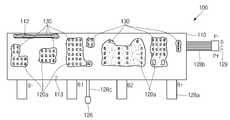
도 1a, 도 1b 및 도 1c는 본 발명의 일 실시예에 따른 전자 소자 보호용 통합 실리콘이 코팅되어 경화된 회로 모듈의 일례를 도시한 평면도, 저면도 및 부분 단면도이다.
도 2는 본 발명의 일 실시예에 따른 전자 소자 보호용 통합 실리콘이 코팅되어 경화된 회로 모듈이 배터리 셀에 전기적으로 연결된 상태를 도시한 회로도의 일례이다.
도 3은 본 발명의 일 실시예에 따른 전자 소자 보호용 통합 실리콘을 이용한 회로 모듈의 제조 방법을 도시한 순서도이다.
도 4는 본 발명의 일 실시예에 따른 전자 소자 보호용 통합 실리콘을 이용한 회로 모듈의 제조 방법을 도시한 개략도이다.1A, 1B, and 1C are plan, bottom, and partial cross-sectional views illustrating an example of a circuit module cured by coating an integrated silicone for electronic device protection according to an embodiment of the present invention.
2 is an example of a circuit diagram showing a state in which a circuit module cured by coating an integrated silicone for electronic device protection according to an embodiment of the present invention is electrically connected to a battery cell.
3 is a flowchart illustrating a method of manufacturing a circuit module using integrated silicon for electronic device protection according to an embodiment of the present invention.
4 is a schematic diagram showing a method of manufacturing a circuit module using integrated silicon for electronic device protection according to an embodiment of the present invention.
이하, 첨부된 도면을 참조하여 본 발명의 바람직한 실시예를 상세히 설명하기로 한다.Hereinafter, preferred embodiments of the present invention will be described in detail with reference to the accompanying drawings.
본 발명의 실시예들은 당해 기술 분야에서 통상의 지식을 가진 자에게 본 발명을 더욱 완전하게 설명하기 위하여 제공되는 것이며, 하기 실시예는 여러 가지 다른 형태로 변형될 수 있으며, 본 발명의 범위가 하기 실시예에 한정되는 것은 아니다. 오히려, 이들 실시예는 본 개시를 더욱 충실하고 완전하게 하고, 당업자에게 본 발명의 사상을 완전하게 전달하기 위하여 제공되는 것이다.The embodiments of the present invention are provided to more completely describe the present invention to those of ordinary skill in the art, and the following examples may be modified in various other forms, and the scope of the present invention is as follows. It is not limited to the examples. Rather, these embodiments are provided to make the present disclosure more faithful and complete, and to completely convey the spirit of the present invention to those skilled in the art.
또한, 이하의 도면에서 각 층의 두께나 크기는 설명의 편의 및 명확성을 위하여 과장된 것이며, 도면상에서 동일 부호는 동일한 요소를 지칭한다. 본 명세서에서 사용된 바와 같이, 용어 "및/또는"은 해당 열거된 항목 중 어느 하나 및 하나 이상의 모든 조합을 포함한다.In addition, in the following drawings, the thickness or size of each layer is exaggerated for convenience and clarity of description, and the same reference numerals refer to the same elements in the drawings. As used herein, the term "and/or" includes any and all combinations of one or more of the corresponding listed items.
본 명세서에서 사용된 용어는 특정 실시예를 설명하기 위하여 사용되며, 본 발명을 제한하기 위한 것이 아니다. 본 명세서에서 사용된 바와 같이, 단수 형태는 문맥상 다른 경우를 분명히 지적하는 것이 아니라면, 복수의 형태를 포함할 수 있다. 또한, 본 명세서에서 사용되는 경우 "포함한다(comprise)" 및/또는 "포함하는(comprising)"은 언급한 형상들, 숫자, 단계, 동작, 부재, 요소 및/또는 이들 그룹의 존재를 특정하는 것이며, 하나 이상의 다른 형상, 숫자, 동작, 부재, 요소 및 /또는 그룹들의 존재 또는 부가를 배제하는 것이 아니다.The terms used in this specification are used to describe specific embodiments, and are not intended to limit the present invention. As used herein, the singular form may include the plural form unless the context clearly indicates another case. Further, as used herein, "comprise" and/or "comprising" specifies the presence of the mentioned shapes, numbers, steps, actions, members, elements and/or groups thereof. And does not exclude the presence or addition of one or more other shapes, numbers, actions, members, elements, and/or groups.
본 명세서에서 제1, 제2 등의 용어가 다양한 부재, 부품, 영역, 층들 및/또는 부분들을 설명하기 위하여 사용되지만, 이들 부재, 부품, 영역, 층들 및/또는 부분들은 이들 용어에 의해 한정되어서는 안 됨은 자명하다. 이들 용어는 하나의 부재, 부품, 영역, 층 또는 부분을 다른 영역, 층 또는 부분과 구별하기 위하여만 사용된다. 따라서, 이하 상술할 제1부재, 부품, 영역, 층 또는 부분은 본 발명의 가르침으로부터 벗어나지 않고서도 제2부재, 부품, 영역, 층 또는 부분을 지칭할 수 있다.In this specification, terms such as first and second are used to describe various members, parts, regions, layers and/or parts, but these members, parts, regions, layers and/or parts are limited by these terms. It is self-evident. These terms are only used to distinguish one member, component, region, layer or portion from another region, layer or portion. Accordingly, the first member, part, region, layer or part to be described below may refer to the second member, part, region, layer or part without departing from the teachings of the present invention.
또한, 본 명세서에서 사용되는 전자 소자는 통상의 능동 소자, 수동 소자 뿐만 아니라, 회로 패턴, 납땜, 와이어 등을 포함할 수 있다. 더욱이, 본 명세서에서 사용되는 회로 모듈은 일반적으로 배터리 셀에 전기적으로 연결된 보호회로모듈을 포함하나, 이로 한정되지 않으며, 배터리 분야 외에 다른 분야의 회로 모듈일 수도 있다. 여기서, 배터리 셀에 보호회로모듈이 전기적으로 연결되면, 배터리 팩으로 지칭되기도 한다.
In addition, electronic devices used in the present specification may include conventional active devices and passive devices, as well as circuit patterns, soldering, and wires. Further, the circuit module used in the present specification generally includes a protection circuit module electrically connected to a battery cell, but is not limited thereto, and may be a circuit module in a field other than the battery field. Here, when the protection circuit module is electrically connected to the battery cell, it is also referred to as a battery pack.
우선, 본 발명에 따른 전자 소자 보호용 통합 실리콘은 베이스 수지, 열 개시제 및 광 개시제를 포함한다. 또한, 본 발명에 따른 통합 실리콘은 정전기 보호용 필러 및/또는 열전도성 필러를 더 포함할 수 있다.First, the integrated silicone for electronic device protection according to the present invention includes a base resin, a thermal initiator, and a photo initiator. In addition, the integrated silicone according to the present invention may further include a filler for static electricity protection and/or a thermally conductive filler.
베이스 수지는 모노머 및 올리고머로 이루어진 군으로부터 선택된 적어도 하나를 포함할 수 있다. 좀더 구체적으로, 베이스 수지는 폴리우레탄 아크릴레이트(Polyurethane acrylate), 이소보닐 아크릴레이트(Isobonyl Acrylate), 모디파이드 아크릴라미드(Modified Acrylamide), 히드록시 에틸 메타크릴레이트(Hydroxy Ethyl Methacrylate) 및 그 등가물로 이루어진 군으로부터 선택된 적어도 하나를 포함한다. 그러나, 본 발명에서 베이스 수지의 재질이 한정되지 않는다. 이러한 베이스 수지는 기본적으로 컨포멀 기능, 방습 기능 및 방진 기능을 갖는다.The base resin may include at least one selected from the group consisting of monomers and oligomers. More specifically, the base resin is polyurethane acrylate, isobonyl acrylate, modified acrylamide, hydroxy ethyl methacrylate and equivalents thereof. It includes at least one selected from the group consisting of. However, the material of the base resin is not limited in the present invention. This base resin basically has a conformal function, a moisture-proof function, and a dust-proof function.
또한, 베이스 수지는, 통합 실리콘을 100wt%로 가정할 경우, 63 내지 68wt%일 수 있다. 베이스 수지가 63wt%보다 작을 경우 통합 실리콘의 점도가 상대적으로 커서 통합 실리콘의 도포가 잘되지 않을 수 있고, 베이스 수지가 68wt%보다 클 경우 통합 실리콘의 점도가 상대적으로 작아서 원하지 않는 영역까지 통합 실리콘이 흘러갈 수 있다. 즉, 베이스 수지가 63 내지 68wt% 이외의 범위를 가질 경우, 통합 실리콘의 작업성이 저하된다.In addition, the base resin may be 63 to 68 wt%, assuming that the integrated silicone is 100 wt%. If the base resin is less than 63wt%, the viscosity of the integrated silicone may be relatively large, so that the application of the integrated silicone may not be good, and if the base resin is larger than 68wt%, the viscosity of the integrated silicone is relatively small, so that the integrated silicone can reach unwanted areas. It can flow. That is, when the base resin has a range other than 63 to 68 wt%, the workability of the integrated silicone is deteriorated.
열 개시제는 실란 커플링 에이전트(Silane Coupling Agent) 및 그 등가물로 이루어진 군으로부터 선택된 적어도 하나를 포함할 수 있다. 그러나, 본 발명에서 열 개시제의 재질이 한정되지 않는다.The thermal initiator may include at least one selected from the group consisting of a silane coupling agent and an equivalent thereof. However, the material of the thermal initiator is not limited in the present invention.
열 개시제는, 통합 실리콘을 100wt%로 가정할 경우, 4.5 내지 5.0wt%일 수 있다. 열 개시제가 4.5wt%보다 작을 경우 통합 실리콘의 열 경화시간이 상대적으로 오래 걸리고, 열 개시제가 5.0wt%보다 클 경우 통합 실리콘의 열 경화 시간 대비 열 개시제가 불필요하게 많아진다.The thermal initiator may be 4.5 to 5.0 wt%, assuming 100 wt% of the integrated silicone. When the thermal initiator is less than 4.5 wt%, the thermal curing time of the integrated silicone takes a relatively long time, and when the thermal initiator is greater than 5.0 wt%, the thermal initiator unnecessarily increases compared to the thermal curing time of the integrated silicone.
광 개시제는, 통합 실리콘을 100wt%로 가정할 경우, 9 내지 10wt%일 수 있다. 광 개시제가 9wt%보다 작을 경우 통합 실리콘의 광 경화시간이 상대적으로 오래 걸리고, 광 개시제가 10wt%보다 클 경우 통합 실리콘의 광 경화 시간 대비 광 개시제가 불필요하게 많아진다.The photoinitiator may be 9 to 10 wt%, assuming that the integrated silicon is 100 wt%. When the photo initiator is less than 9 wt%, the photo-curing time of the integrated silicone takes a relatively long time, and when the photo initiator is larger than 10 wt%, the photo-initiator is unnecessarily increased compared to the photo-curing time of the integrated silicone.
정전기 보호용 필러는 알루미늄 옥사이드(Al2O3), 알루미늄 히드록사이드(AlO), 틴디옥사이드(SnO2), 징크옥사이드(ZnO) 및 그 등가물로 이루어진 군으로부터 선택된 적어도 하나를 포함할 수 있다. 그러나, 본 발명에서 정전기 보호용 필러의 재질이 한정되지 않는다. 경우에 따라 하기할 열전도성 필러 역시 정전기 보호 역할을 할 수도 있다.The static electricity protection filler may include at least one selected from the group consisting of aluminum oxide (Al2O3), aluminum hydroxide (AlO), tin dioxide (SnO2), zinc oxide (ZnO), and equivalents thereof. However, in the present invention, the material of the filler for protecting static electricity is not limited. In some cases, a thermally conductive filler to be described below may also serve as static electricity protection.
더불어, 열전도성 필러는 흄드 실리카(Fumed Silica), 마그네슘 옥사이드(MgO), 보론나이트라이드(BN), 알루미늄나이트라이드(AlN) 및 그 등가물로 이루어진 군으로부터 선택된 적어도 하나를 포함할 수 있다. 그러나, 본 발명에서 열전도성 필러의 재질이 한정되지 않는다. 경우에 따라 상술한 정전기 보호용 필러 역시 열전도 역할을 할 수 있다.In addition, the thermally conductive filler may include at least one selected from the group consisting of fumed silica, magnesium oxide (MgO), boron nitride (BN), aluminum nitride (AlN), and equivalents thereof. However, in the present invention, the material of the thermally conductive filler is not limited. In some cases, the aforementioned filler for protecting static electricity may also serve as a heat conduction.
한편, 정전기 보호용 필러 및 열전도성 필러는, 통합 실리콘을 100wt%로 가정할 경우, 22 내지 23wt%일 수 있다. 정전기 보호용 필러 및 열전도성 필러는 22wt%보다 작을 경우 통합 실리콘의 통합 실리콘의 점도가 상대적으로 작아서 원하지 않는 영역까지 통합 실리콘이 흘러갈 수 있고, 정전기 보호용 필러 및 열전도성 필러가 23wt%보다 클 경우 통합 실리콘의 점도가 상대적으로 커서 통합 실리콘의 도포가 잘되지 않을 수 있다. 즉, 정전기 보호용 필러 및 열전도성 필러가 22 내지 23wt% 이외의 범위를 가질 경우, 통합 실리콘의 작업성이 저하된다.On the other hand, the static electricity protection filler and the thermally conductive filler may be 22 to 23 wt%, assuming that the integrated silicon is 100 wt%. Electrostatic protection filler and thermally conductive filler are integrated in the integrated silicone when less than 22wt% The viscosity of the integrated silicone is relatively small, so the integrated silicone can flow to unwanted areas, and integrated when the electrostatic protection filler and thermally conductive filler are greater than 23wt% The viscosity of the silicone is relatively large, so the application of the integrated silicone may not be good. That is, when the static electricity protection filler and the thermally conductive filler have a range other than 22 to 23 wt%, the workability of the integrated silicone is deteriorated.
도 1a, 도 1b 및 도 1c를 참조하면, 본 발명의 일 실시예에 따른 전자 소자 보호용 통합 실리콘(130)이 코팅되어 경화된 회로 모듈(100)의 일례가 평면도, 저면도 및 부분 단면도로서 도시되어 있다.1A, 1B, and 1C, an example of a
도 1a 내지 도 1c에 도시된 바와 같이, 본 발명의 일 실시예에 따른 회로 모듈(100)은 인쇄회로기판(110), 다수의 전자 소자(120) 및 코팅되어 경화된 통합 실리콘(130)을 포함한다.1A to 1C, the
인쇄회로기판(110)은 절연층(111)을 중심으로 표면에 다수의 회로패턴(112)이 형성되어 있으며, 회로패턴(112)의 대부분은 솔더 마스크와 같은 보호층(113)으로 덮여 있다. 이러한 인쇄회로기판(110)은 경성 회로기판, 연성 회로기판 및 그 등가물 중 어느 하나를 포함한다.A plurality of
다수의 전자 소자(120)는 인쇄회로기판(110)에 구비된 회로패턴(112)에 솔더(120a)를 통하여 전기적으로 접속된다. 예를 들어, 전자 소자(120)는 집적회로 반도체 패키지(121), 트랜지스터(122a,122b), 저항(123), 커패시터(124), 양성온도소자(125), 온도 센서(126) 또는/및 퓨즈(127) 등을 포함한다. 여기서, 집적회로 반도체 패키지(121)는 마이크로 프로세서 유닛일 수 있으며, 트랜지스터(122a,122b)는 충전 제어 스위치 및 방전 제어 스위치일 수 있다.The plurality of
또한, 적어도 하나의 와이어(128a,128b,128c)가 인쇄회로기판(110)에 구비된 회로패턴(112)에 솔더(120a)를 통하여 전기적으로 접속될 수 있다. 일례로 와이어(128a)는 회로 모듈(100)과 배터리 셀(210)을 전기적으로 연결하는 리드 플레이트를 포함할 수 있다. 또한, 와이어(128b)는 배터리 팩(200)과 외부 셋트를 전기적으로 연결하는 커넥터(129)에 연결될 수 있다. 더불어, 와이어(128c)는 배터리 셀(210)의 온도 센싱을 위해 온도 센서(126)에 연결될 수 있다.In addition, at least one
여기서, 이러한 회로모듈(100)은 본 발명의 이해를 위한 일례일 뿐이며, 도면에 도시된 회로모듈(100)로 본 발명이 한정되는 것은 아니다.Here, the
한편, 통합 실리콘(130)은 회로패턴(112), 솔더(120a) 및 전자 소자(120) 중 적어도 하나에 코팅되어 경화된다. 즉, 통합 실리콘(130)은 컨포멀, 방습, 방진, 열전도 및 정전기 방지 기능을 갖는다. 다르게 설명하면, 통합 실리콘(130)은 외부의 물리적, 화학적 환경으로부터 회로패턴(112), 솔더(120a) 또는/및 전자 소자(120) 등을 보호한다.Meanwhile, the
좀더 구체적으로, 통합 실리콘(130)은 전자 소자(120)로 수분이 침투하는 현상을 방지한다. 또한, 통합 실리콘(130)은 전자 소자(120)로 진동이 전달되는 현상을 방지한다. 또한, 통합 실리콘(130)은 전자 소자(120)(예를 들면, 집적회로 반도체 패키지(121), 트랜지스터(122a,122b))에서 발생하는 열이 외부로 신속히 방출되도록 한다. 또한, 통합 실리콘(130)은 배터리 셀(210) 또는 그 주변 온도가 전자 소자(120)(예를 들면, 양성온도소자(125))로 신속히 전달되도록 한다. 더욱이, 통합 실리콘(130)은 예를 들면 회로패턴(112), 솔더(120a) 및 전자 소자(120)로 정전기가 유입되지 않도록 한다. 또한, 이러한 통합 실리콘(130)은 내부의 필러 등의 영향으로 백색일 수 있다. 그러나, 이러한 색상으로 본 발명의 통합 실리콘(130)이 한정되지 않는다. 물론, 이러한 통합 실리콘(130)은 상술한 베이스 수지, 열 개시제, 광 개시제, 정전기 보호용 필러 및/또는 열전도성 필러를 포함한다.More specifically, the
더불어, 회로패턴(112)과 와이어(128a,128b,128c)의 연결 영역(예를 들면, 솔더(120a))에 고정용 에폭시 수지(140)가 더 코팅될 수 있다. 여기서, 고정용 에폭시 수지(140)는 내부 상태의 관찰이 가능하도록 투명할 수 있다. 그러나, 이러한 색상으로 본 발명의 통합 실리콘(130)이 한정되지 않는다. 이러한 고정용 에폭시 수지(140)는 강력한 접착력, 우수한 작업성 및 속경화 특징을 갖는 통상의 전자 부품 고정용 에폭시 수지일 수 있다.In addition, the fixing epoxy resin 140 may be further coated on the connection region (eg,
도 2를 참조하면, 본 발명의 일 실시예에 따른 전자 소자 보호용 통합 실리콘(130)이 코팅되어 경화된 회로 모듈(100)이 배터리 셀(210)에 전기적으로 연결된 상태의 회로도가 도시되어 있다.Referring to FIG. 2, a circuit diagram of a
상술한 바와 같이 배터리 팩(200)은 적어도 하나의 배터리 셀(210)과, 배터리 셀(210)의 과충전이나 과방전을 방지하도록 하는 보호회로모듈을 포함한다. 여기서, 보호회로모듈이 상술한 회로 모듈(100)일 수 있다.As described above, the
도 2에 도시된 바와 같이, 회로 모듈(100)은 배터리 셀(210)에 와이어(128a)(또는 리드 플레이트나 연성회로기판도 가능함)를 통해 전기적으로 연결될 수 있다. 또한, 회로 모듈(100)은 커넥터(129)에 와이어(128b)를 통해 전기적으로 연결되며, 이러한 커넥터(129)는 외부 셋트 또는 충전기에 연결될 수 있다. 물론, 커넥터(129)는 와이어없이 인쇄회로기판(110)에 직접 실장될 수도 있다. 더불어, 회로 모듈(100)은 집적회로 반도체 패키지(121), 트랜지스터(122a,122b), 전류 센서(저항(123)), 양성온도소자(125), 온도 센서(126) 및 퓨즈(127) 등을 포함한다. 이러한 회로는 본 발명의 이해를 위한 일례일 뿐이며, 본 발명이 도 2에 도시된 회로로 한정되는 것은 아니다.As shown in FIG. 2, the
한편, 배터리 셀(210)은 통상의 각형 배터리, 원통형 배터리 또는 파우치형 배터리일 수 있으며, 본 발명에서 배터리의 종류가 한정되는 것은 아니다.Meanwhile, the
도 3 및 도 4를 참조하면, 본 발명의 일 실시예에 따른 전자 소자 보호용 통합 실리콘(130)을 이용한 회로 모듈(100)의 제조 방법이 도시되어 있다. 여기서, 도 1a 내지 도 1c를 함께 참조한다.3 and 4, a method of manufacturing the
본 발명에 따른 회로 모듈(100)의 제조 방법은 인쇄회로기판 구비 단계(S1), 통합 실리콘 코팅 단계(S2), 그리고 광 및 열 경화 단계(S4)를 포함한다. 또한, 본 발명은 와이어 고정용 에폭시 수지 코팅 단계(S3)를 포함할 수 있다.The manufacturing method of the
인쇄회로기판 구비 단계(S1)에서는, 절연층(111) 위에 다수의 회로패턴(112)이 형성된 인쇄회로기판(110)이 구비되고, 회로패턴(112)에 다수의 전자 소자(120)가 솔더(120a)에 의해 전기적으로 연결된다. 여기서, 전자 소자(120)는 집적회로 반도체 패키지(121), 트랜지스터(122a,122b), 저항(123), 커패시터(124), 양성온도소자(125), 온도 센서(126), 퓨즈(127) 등일 수 있다. 또한, 이때 각종 와이어(128a,128b,128c)가 인쇄회로기판(110)에 솔더(120a)에 의해 전기적으로 접속될 수 있다.In the step of providing a printed circuit board (S1), a printed
통합 실리콘 코팅 단계(S2)에서는, 회로패턴(112), 솔더(120a) 및/또는 전자 소자(120)에 통합 실리콘(130)이 코팅된다. 여기서, 통합 실리콘(130)은 상술한 바와 같이 컨포멀 기능, 방습 기능, 방진 기능, 열전도 기능 및 정전기 보호 기능을 갖는다. 따라서, 종래의 컨포멀 실리콘 코팅, 방습 실리콘 코팅, 방진 실리콘 코팅, 열전도성 실리콘 코팅 및 정전기 보호 실리콘 코팅과 같은 다수의 단계로 이루어진 코팅 공정이 본 발명에서 1단계 코팅 공정으로 완료된다.In the integrated silicon coating step S2, the
더불어, 회로패턴(112)과 와이어(128a,128b,128c)의 연결 영역에도 고정용 에폭시 수지(140)가 더 코팅될 수 있다.(단계 S3) 여기서, 고정용 에폭시 수지(140)는 통상의 자외선 경화 수지일 수 있다.In addition, the fixing epoxy resin 140 may be further coated on the connection area between the
광 및 열 경화 단계(S4)에서는, 통합 실리콘(130)이 광(예를 들면, 자외선) 및 열에 의해 경화된다. 물론, 고정용 에폭시 수지(140)도 광 경화된다.In the light and thermal curing step S4, the
이때, 광의 파장은 대략 300nm 내지 500nm로 제어되고, 열에 의한 온도는 대략 60℃ 내지 100℃로 제어되며, 또한, 광 및 열을 이용한 경화 단계는 대략 10초 내지 60초 동안 수행될 수 있다. 광의 파장이 300nm보다 작거나 500nm보다 클 경우 광 경화가 이루어지지 않는다. 또한, 온도가 60℃보다 작을 경우 열 경화가 이루어지지 않고, 또한 온도가 100℃보다 클 경우 전자 소자가 파손될 수 있다. 더불어, 경화 시간이 10초보다 작을 경우 광 경화 또는/및 열 경화가 제대로 이루어지지 않고, 시간이 60초보다 클 경우 불필요하게 경화 시간이 길어진다.At this time, the wavelength of light is controlled to be about 300 nm to 500 nm, the temperature by heat is controlled to about 60 to 100°C, and the curing step using light and heat may be performed for about 10 to 60 seconds. If the wavelength of light is less than 300nm or greater than 500nm, photocuring is not performed. In addition, when the temperature is less than 60°C, thermal curing is not performed, and when the temperature is greater than 100°C, the electronic device may be damaged. In addition, when the curing time is less than 10 seconds, photocuring or/and thermal curing is not properly performed, and when the time is greater than 60 seconds, the curing time is unnecessarily lengthened.
한편, 통합 실리콘(130)의 광 경화 시 그림자 영역에서 미경화 현상이 발생할 수 있으나, 상술한 바와 같이 광원(351)으로부터 발생하는 열에 의해 통합 실리콘(130)이 열 경화됨으로써, 통합 실리콘(130)의 전체적인 경화 시간이 짧고 경화 성능이 우수하다.On the other hand, when the
여기서, 모든 단계는 컨베이어 벨트(310) 위에서 수행될 수 있으며, 컨베이어 벨트(310)는 롤러(320)에 결합되어 일측 방향으로 회전한다. 더불어, 컨베이어 벨트(310) 위에 전자 소자(120)의 고정 및 솔더링 툴(330)이 위치되고, 또한 통합 실리콘(130)의 도포를 위한 실린더(340)가 위치된다. 더불어, 컨베이어 벨트(310) 위에 광 및 열 경화를 위해 광원(351) 및 배기팬(352)을 갖는 챔버(350)가 위치된다.Here, all steps may be performed on the
또한, 광 및 열 경화가 수행되는 챔버(350)의 내부 온도는 배기팬(352)에 의해 제어될 수 있다. 즉, 기본적으로 광원(351)에 의해 주변 온도가 100℃보다 높게 상승할 수 있으나, 배기팬(352)의 제어에 의해 챔버(350)의 내부 온도가 60℃ 내지 100℃로 제어될 수 있다.In addition, the internal temperature of the
아래의 표 1은 고온 다습(High temperature and high humidity) 테스트 조건을 도시한 것이며, 이러한 고온 다습 테스트 조건하에서 본 발명이 적용된 회로 모듈의 전자 소자(즉, 집적회로 반도체 패키지, 회로 패턴, 솔더 등등)는 습기에 의해 부식되지 않음을 확인하였다.Table 1 below shows the high temperature and high humidity test conditions, and the electronic devices of the circuit module to which the present invention is applied (i.e., integrated circuit semiconductor package, circuit pattern, solder, etc.) under such high temperature and high humidity test conditions It was confirmed that it was not corroded by moisture.
아래의 표 2는 정전기 테스트 조건을 도시한 것이며, 이러한 정전기 테스트 조건하에서 본 발명이 적용된 회로 모듈은 전기적으로 손상되지 않았다. 여기서, 종래 기술은 회로 모듈에 컨포멀 실리콘 코팅, 방습 실리콘 코팅, 방진 실리콘 코팅, 열전도 실리콘 코팅 및 정전기 보호 실리콘 코팅이 각각 이루어진 회로 모듈을 의미한다. 더불어, "접촉"은 전자 소자에 접촉된 상태로 정전기가 인가됨을 의미하고, "공기"는 전자 소자로부터 이격된 상태로 정전기가 인가됨을 의미한다.Table 2 below shows electrostatic test conditions, and under these electrostatic test conditions, the circuit module to which the present invention is applied was not electrically damaged. Here, the prior art refers to a circuit module in which a conformal silicone coating, a moisture-proof silicone coating, a dust-proof silicone coating, a thermally conductive silicone coating, and an electrostatic protection silicone coating are respectively formed on the circuit module. In addition, "contact" means that static electricity is applied while being in contact with the electronic device, and "air" means that static electricity is applied while being separated from the electronic device.
기술Conventional
Technology
발명example
invent
아래 표 3은 본 발명이 적용된 회로 모듈 즉, 통합 실리콘에서 유해 물질의 검출 여부를 도시한 것이며, 표 3에 도시된 바와 같이 본 발명에 따른 통합 실리콘에서 유해 물질은 검출되지 않았다. 여기서, 유해 물질의 검출을 위해 XRF(X-Ray Flourescence Spectrometry)가 이용되었다.Table 3 below shows whether or not harmful substances are detected in the circuit module to which the present invention is applied, that is, integrated silicon, and as shown in Table 3, no harmful substances were detected in the integrated silicon according to the present invention. Here, XRF (X-Ray Flourescence Spectrometry) was used to detect harmful substances.
아래의 표 4는 본 발명이 적용된 회로 모듈 중에서 와이어의 인장 강도 테스트 결과를 도시한 것이다. 통상 와이어 1개당 1kgf 이상의 인장 강도를 가지면 정상으로 본다.Table 4 below shows the results of a tensile strength test of a wire in a circuit module to which the present invention is applied. Normally, a tensile strength of 1kgf or more per wire is considered normal.
아래의 표 5는 본 발명에 따른 회로 모듈이 장착된 배터리 팩을 고온 다습(50℃, 85%RH, 48hrs) 환경에 적용하기 이전 및 이후의 전기적 기능을 테스트한 결과를 도시한 것이다. 일례로, 배터리 팩의 OCV, IR, 충전/방전, 통신, 외관 및 누전 상황은 고온 다습 환경에 적용하기 이전 및 이후에 있어 모두 정상으로 판정되었다. 여기서, OCV(open circuit voltage)는 배터리 셀로부터 외부로 전류가 흐르지 않는 상태에서의 배터리 셀 전압을 의미하고, IR은 배터리 셀의 내부 저항을 의미하며, 이러한 OCV/IR은 배터리 팩의 양/불 판정을 하는 주요 기준이다.Table 5 below shows the results of testing the electrical function before and after applying the battery pack equipped with the circuit module according to the present invention to a high temperature and high humidity (50°C, 85%RH, 48hrs) environment. For example, OCV, IR, charge/discharge, communication, appearance, and leakage conditions of the battery pack were all determined to be normal before and after application to a high temperature and high humidity environment. Here, OCV (open circuit voltage) refers to the battery cell voltage in a state in which no current flows from the battery cell to the outside, IR refers to the internal resistance of the battery cell, and OCV/IR refers to the positive/negative battery pack It is the main criterion for judging.
방전charge
Discharge
방전charge
Discharge
아래의 표 6은 본 발명에 따른 회로 모듈이 장착된 배터리 팩을 정전기 환경(접촉 -8kV, 공기 -15kV)에 적용하기 이전 및 이후의 전기적 기능을 테스트한 결과이다. 일례로, 배터리 팩의 OCV, IR, 충전/방전, 통신, 외관 및 누전 상황은 정전기 환경에 적용하기 이전 및 이후에 있어 모두 정상으로 판정되었다.Table 6 below is a result of testing the electrical function before and after applying the battery pack equipped with the circuit module according to the present invention to an electrostatic environment (contact -8kV, air -15kV). For example, OCV, IR, charge/discharge, communication, appearance, and leakage conditions of the battery pack were all determined to be normal before and after application to an electrostatic environment.
Short circuit
방전charge
Discharge
방전charge
Discharge
방전charge
Discharge
이와 같이 하여, 본 발명의 일 실시예는 컨포멀 기능, 방습 기능, 방진 기능, 열전도 기능 및 정전기 보호 기능을 가질 뿐만 아니라 경화 시간이 60초 이내인 전자 소자 보호용 통합 실리콘, 이를 이용한 회로 모듈 및 이의 제조 방법을 제공한다.In this way, an embodiment of the present invention has a conformal function, a moisture-proof function, a dust-proof function, a heat conduction function and an electrostatic protection function, as well as an integrated silicone for protecting electronic devices having a curing time of less than 60 seconds, a circuit module using the same, and a circuit module thereof. Provides a manufacturing method.
더불어, 본 발명의 일 실시예에 따른 회로 모듈을 갖는 배터리 팩은 고온 다습 환경/정전기 환경 하에서도 정상적인 OCV, IR, 충전/방전, 통신, 외관을 가지며, 또한 누전이 발생하지 않는다.In addition, the battery pack having a circuit module according to an embodiment of the present invention has a normal OCV, IR, charge/discharge, communication, and appearance even under a high-temperature and high-humidity environment/electrostatic environment, and does not generate a short circuit.
따라서, 본 발명의 일 실시예에 따른 통합 실리콘은 회로 모듈(보호회로모듈) 및 이를 갖는 배터리 팩의 제조 시간을 극적으로 감소시키면서도, 고온 다습 환경/정전기 환경 하에서도 정상적인 전기적 성능을 보증하도록 한다.
Accordingly, the integrated silicon according to an embodiment of the present invention dramatically reduces the manufacturing time of a circuit module (protection circuit module) and a battery pack having the same, while ensuring normal electrical performance even in a high temperature and high humidity environment/electrostatic environment.
이상에서 설명한 것은 본 발명에 따른 전자 소자 보호용 통합 실리콘, 이를 이용한 회로 모듈 및 이의 제조 방법를 실시하기 위한 하나의 실시예에 불과한 것으로서, 본 발명은 상기한 실시예에 한정되지 않고, 이하의 특허청구범위에서 청구하는 바와 같이 본 발명의 요지를 벗어남이 없이 당해 발명이 속하는 분야에서 통상의 지식을 가진 자라면 누구든지 다양한 변경 실시가 가능한 범위까지 본 발명의 기술적 정신이 있다고 할 것이다.What has been described above is only one embodiment for implementing the integrated silicon for electronic device protection according to the present invention, a circuit module using the same, and a method for manufacturing the same, and the present invention is not limited to the above-described embodiment, and the following claims As claimed in the foregoing, any person of ordinary skill in the field to which the present invention pertains without departing from the gist of the present invention will have the technical spirit of the present invention to the extent that various modifications can be implemented.
100; 회로 모듈110; 인쇄회로기판
111; 절연층112; 회로패턴
113; 보호층120; 전자 소자
120a; 솔더121; 집적회로 반도체 패키지
122a, 122b; 트랜지스터123; 저항
124; 커패시터125; 양성온도소자
126; 온도 센서127; 퓨즈
128a, 128b, 128b; 와이어129; 커넥터
130; 통합 실리콘140; 고정용 에폭시 수지
200; 배터리 팩210; 배터리 셀100;
111; Insulating
113;
120a;
122a, 122b;
124;
126;
128a, 128b, 128b;
130; Integrated silicone 140; Epoxy resin for fixing
200;
Claims (20)
Translated fromKorean절연층 위에 다수의 회로패턴이 형성되고, 상기 회로패턴이 솔더 마스크 보호층으로 덮여 있는 인쇄회로기판; 및,
상기 회로패턴에 솔더에 의해 전기적으로 접속된 다수의 전자 소자를 포함하고,
상기 솔더 마스크 보호층을 통해 노출된 상기 회로패턴과, 상기 솔더와, 상기 전자 소자에 상기 전자 소자 보호용 실리콘이 코팅되어 경화되고,
상기 전자 소자 보호용 실리콘은 정전기 보호용 필러 및 열전도성 필러를 더 포함하고, 상기 전자 소자 보호용 실리콘 중 상기 정전기 보호용 필러 및 열전도성 필러는 22 내지 23wt%인, 회로 모듈.Silicon for electronic device protection;
A printed circuit board on which a plurality of circuit patterns are formed on an insulating layer, and the circuit patterns are covered with a solder mask protective layer; And,
Including a plurality of electronic elements electrically connected to the circuit pattern by solder,
The circuit pattern exposed through the solder mask protective layer, the solder, and the electronic device are coated with and cured with the electronic device protective silicon,
The electronic device protection silicon further includes a static electricity protection filler and a thermal conductive filler, and the static electricity protection filler and the thermal conductive filler among the electronic device protection silicon are 22 to 23 wt%.
상기 전자 소자 보호용 실리콘은 모노머 또는 올리고머를 포함하는 베이스 수지; 열 개시제; 및 광 개시제를 포함하는, 회로 모듈.The method of claim 1,
The silicone for protecting electronic devices is a base resin containing a monomer or oligomer; Thermal initiator; And a photoinitiator.
상기 전자 소자 보호용 실리콘 중 상기 베이스 수지는 63 내지 68wt%인, 회로 모듈.The method of claim 2,
In the electronic device protection silicon, the base resin is 63 to 68wt%, a circuit module.
상기 베이스 수지는 폴리우레탄 아크릴레이트(Polyurethane acrylate), 이소보닐 아크릴레이트(Isobonyl Acrylate), 모디파이드 아크릴라미드(Modified Acrylamide) 및 히드록시 에틸 메타크릴레이트(Hydroxy Ethyl Methacrylate)로 이루어진 군으로부터 선택된 적어도 하나를 포함하는, 회로 모듈.The method of claim 2,
The base resin is at least one selected from the group consisting of Polyurethane acrylate, Isobonyl Acrylate, Modified Acrylamide, and Hydroxy Ethyl Methacrylate Containing, a circuit module.
상기 열 개시제는 실란 커플링 에이전트(Silane Coupling Agent)를 포함하는, 회로 모듈.The method of claim 2,
The circuit module, wherein the thermal initiator comprises a Silane Coupling Agent.
상기 전자 소자 보호용 실리콘 중 상기 열 개시제는 4.5 내지 5.0wt%인, 회로 모듈.The method of claim 2,
The thermal initiator of the silicon for electronic device protection is 4.5 to 5.0wt%, the circuit module.
상기 전자 소자 보호용 실리콘 중 상기 광 개시제는 9 내지 10wt%인, 회로 모듈.The method of claim 2,
In the electronic device protection silicon, the photo initiator is 9 to 10 wt%, a circuit module.
상기 정전기 보호용 필러는 알루미늄 옥사이드(Al2O3), 알루미늄 히드록사이드(AlO), 틴디옥사이드(SnO2) 및 징크옥사이드(ZnO)로 이루어진 군으로부터 선택된 적어도 하나를 포함하는, 회로 모듈.The method of claim 1,
The static electricity protection filler comprises at least one selected from the group consisting of aluminum oxide (Al2O3), aluminum hydroxide (AlO), tin dioxide (SnO2), and zinc oxide (ZnO).
상기 열전도성 필러는 흄드 실리카(Fumed Silica), 마그네슘 옥사이드(MgO), 보론나이트라이드(BN) 및 알루미늄나이트라이드(AlN)로 이루어진 군으로부터 선택된 적어도 하나를 포함하는, 회로 모듈.The method of claim 1,
The thermally conductive filler comprises at least one selected from the group consisting of fumed silica, magnesium oxide (MgO), boron nitride (BN), and aluminum nitride (AlN).
상기 회로패턴에 전기적으로 연결된 적어도 하나의 와이어를 더 포함하고,
상기 회로패턴과 상기 와이어의 연결 영역에 코팅된 고정용 에폭시 수지를 더 포함하는, 회로 모듈.The method of claim 1,
Further comprising at least one wire electrically connected to the circuit pattern,
The circuit module further comprising a fixing epoxy resin coated on the connection region between the circuit pattern and the wire.
상기 와이어에 적어도 하나의 배터리 셀, 적어도 하나의 온도 센서, 또는 적어도 하나의 커넥터가 전기적으로 연결되는, 회로 모듈.The method of claim 13,
At least one battery cell, at least one temperature sensor, or at least one connector is electrically connected to the wire.
상기 전자 소자는 집적회로 반도체 패키지, 트랜지스터, 저항, 캐패시터, 양성온도소자 및 퓨즈로 이루어진 군으로부터 선택된 적어도 하나를 포함하는, 회로 모듈.The method of claim 1,
The electronic device includes at least one selected from the group consisting of an integrated circuit semiconductor package, a transistor, a resistor, a capacitor, a positive temperature device, and a fuse.
상기 솔더 마스크 보호층을 통해 노출된 상기 회로패턴, 상기 솔더 및 상기 전자 소자에 제1항에 기재된 실리콘을 코팅하는 단계; 및
상기 실리콘을 광 및 열을 이용해 경화하는 단계를 포함하는, 회로 모듈의 제조 방법.Providing a printed circuit board in which a plurality of circuit patterns are formed on an insulating layer, the circuit pattern is covered with a solder mask protective layer, and electrically connecting a plurality of electronic devices to the circuit pattern using solder;
Coating the silicon of claim 1 on the circuit pattern, the solder, and the electronic device exposed through the solder mask protective layer; And
A method of manufacturing a circuit module comprising curing the silicon using light and heat.
상기 광 및 열을 이용해 경화하는 단계는 상기 광의 파장이 300nm 내지 500nm로 제어되도록 하고, 상기 열에 의한 온도가 60℃ 내지 100℃로 제어되도록 하는, 회로 모듈의 제조 방법.The method of claim 16,
The step of curing using light and heat is such that the wavelength of the light is controlled to 300 nm to 500 nm, and the temperature by the heat is controlled to 60 to 100° C., a method of manufacturing a circuit module.
상기 광 및 열을 이용해 경화하는 단계는 10초 내지 60초 동안 수행되는, 회로 모듈의 제조 방법.The method of claim 16,
The step of curing using light and heat is performed for 10 seconds to 60 seconds, a method of manufacturing a circuit module.
상기 전자 소자를 전기적으로 연결하는 단계에서 상기 전자 소자는 집적회로 반도체 패키지, 트랜지스터, 저항, 캐패시터, 양성온도소자 및 퓨즈로 이루어진 군으로부터 선택된 적어도 하나를 포함하는, 회로 모듈의 제조 방법.The method of claim 16,
In the step of electrically connecting the electronic device, the electronic device includes at least one selected from the group consisting of an integrated circuit semiconductor package, a transistor, a resistor, a capacitor, a positive temperature device, and a fuse.
상기 전자 소자를 전기적으로 연결하는 단계는 상기 회로패턴에 적어도 하나의 와이어를 연결하는 단계를 더 포함하고,
상기 광 및 열을 이용해 경화하는 단계 이전에 상기 회로패턴과 상기 와이어의 연결 영역에 고정용 에폭시 수지를 코팅하는 단계를 더 포함하는, 회로 모듈의 제조 방법.The method of claim 16,
Electrically connecting the electronic device further includes connecting at least one wire to the circuit pattern,
The method of manufacturing a circuit module further comprising coating a fixing epoxy resin on a connection region between the circuit pattern and the wire before the curing using light and heat.
Priority Applications (6)
| Application Number | Priority Date | Filing Date | Title |
|---|---|---|---|
| KR1020130141785AKR102177502B1 (en) | 2013-11-20 | 2013-11-20 | Integrated silicone for protecting electronic devices, circuit module using the same, and the method thereof |
| US14/537,250US9834686B2 (en) | 2013-11-20 | 2014-11-10 | Integrated silicone for protecting electronic devices, circuit module using the same and manufacturing method of circuit module |
| PL14193750.8TPL2876138T3 (en) | 2013-11-20 | 2014-11-18 | Silicone material for protecting electronic devices, circuit module using the same and manufacturing method of circuit module |
| EP14193750.8AEP2876138B1 (en) | 2013-11-20 | 2014-11-18 | Silicone material for protecting electronic devices, circuit module using the same and manufacturing method of circuit module |
| HUE14193750AHUE065989T2 (en) | 2013-11-20 | 2014-11-18 | Silicone material for protecting electronic devices, circuit module using the same and manufacturing method of circuit module |
| JP2014234898AJP6504649B2 (en) | 2013-11-20 | 2014-11-19 | Silicon-containing composition for protecting electronic device, circuit module using the same, and method for producing the same |
Applications Claiming Priority (1)
| Application Number | Priority Date | Filing Date | Title |
|---|---|---|---|
| KR1020130141785AKR102177502B1 (en) | 2013-11-20 | 2013-11-20 | Integrated silicone for protecting electronic devices, circuit module using the same, and the method thereof |
Publications (2)
| Publication Number | Publication Date |
|---|---|
| KR20150057886A KR20150057886A (en) | 2015-05-28 |
| KR102177502B1true KR102177502B1 (en) | 2020-11-11 |
Family
ID=51904792
Family Applications (1)
| Application Number | Title | Priority Date | Filing Date |
|---|---|---|---|
| KR1020130141785AActiveKR102177502B1 (en) | 2013-11-20 | 2013-11-20 | Integrated silicone for protecting electronic devices, circuit module using the same, and the method thereof |
Country Status (6)
| Country | Link |
|---|---|
| US (1) | US9834686B2 (en) |
| EP (1) | EP2876138B1 (en) |
| JP (1) | JP6504649B2 (en) |
| KR (1) | KR102177502B1 (en) |
| HU (1) | HUE065989T2 (en) |
| PL (1) | PL2876138T3 (en) |
Families Citing this family (8)
| Publication number | Priority date | Publication date | Assignee | Title |
|---|---|---|---|---|
| WO2018111306A1 (en)* | 2016-12-16 | 2018-06-21 | Syed Taymur Ahmad | Process for protecting an electronic device by selective deposition of polymer coatings |
| KR102033001B1 (en)* | 2017-02-28 | 2019-10-16 | 주식회사 유라코퍼레이션 | Frame assembly, method of manufacturing frame assembly, and method of manufacturing battery module |
| JP6383885B2 (en)* | 2017-01-27 | 2018-08-29 | モメンティブ・パフォーマンス・マテリアルズ・ジャパン合同会社 | Thermally conductive polyorganosiloxane composition |
| KR102186090B1 (en)* | 2017-06-15 | 2020-12-03 | 주식회사 엘지화학 | Apparatus and method for partially molding of printed circuit board, and printed circuit board produced therefrom |
| KR102217451B1 (en)* | 2017-08-29 | 2021-02-22 | 주식회사 엘지화학 | Rechargeable battery and the manufacturing method, and press block for rechargeable battery |
| CN111816570A (en)* | 2019-07-05 | 2020-10-23 | 北京荷清柔创科技有限公司 | Flexible electronic device and preparation method and preparation device thereof |
| US11570903B2 (en)* | 2019-10-16 | 2023-01-31 | Advanced Micro Devices, Inc. | Process for conformal coating of multi-row surface-mount components in a lidless BGA package and product made thereby |
| US12226628B2 (en)* | 2020-12-16 | 2025-02-18 | Oscor Inc. | Method to manufacture cuff leads |
Citations (1)
| Publication number | Priority date | Publication date | Assignee | Title |
|---|---|---|---|---|
| WO2010143379A1 (en)* | 2009-06-08 | 2010-12-16 | パナソニック株式会社 | Method of producing electronic component mounting structure, and electronic component mounting structure |
Family Cites Families (19)
| Publication number | Priority date | Publication date | Assignee | Title |
|---|---|---|---|---|
| JPS63230705A (en)* | 1987-03-19 | 1988-09-27 | Toyobo Co Ltd | Ultraviolet-curable resin composition |
| US5557142A (en)* | 1991-02-04 | 1996-09-17 | Motorola, Inc. | Shielded semiconductor device package |
| US6099783A (en)* | 1995-06-06 | 2000-08-08 | Board Of Trustees Operating Michigan State University | Photopolymerizable compositions for encapsulating microelectronic devices |
| CN1433443B (en)* | 1999-12-07 | 2010-05-12 | 威廉马歇莱思大学 | Oriented Nanofibers Embedded in a Polymer Matrix |
| JP4180844B2 (en) | 2002-06-06 | 2008-11-12 | 昭和電工株式会社 | Curable flame retardant composition, cured product thereof and production method thereof |
| JP2004022524A (en) | 2002-06-20 | 2004-01-22 | Sanyo Gs Soft Energy Co Ltd | Battery and battery pack |
| JP2004247159A (en) | 2003-02-13 | 2004-09-02 | Sanyo Gs Soft Energy Co Ltd | Battery pack and its manufacturing method |
| JP3879682B2 (en)* | 2003-03-10 | 2007-02-14 | 株式会社デンソー | Circuit board manufacturing method |
| JP2004289070A (en)* | 2003-03-25 | 2004-10-14 | Seiko Epson Corp | Wiring board and method of manufacturing the same, semiconductor device, electronic device, and electronic equipment |
| US7342311B2 (en)* | 2004-09-13 | 2008-03-11 | Lawrence Livermore National Security, Llc | Electronic unit integrated into a flexible polymer body |
| KR100539473B1 (en) | 2005-11-24 | 2005-12-28 | 주식회사 파워로직스 | Inner pack battery and method of manufacturing the same |
| EP1999529B1 (en)* | 2006-03-28 | 2014-07-16 | Parker-Hannifin Corporation | Dispensable cured resin |
| JP2009102574A (en)* | 2007-10-25 | 2009-05-14 | Sekisui Chem Co Ltd | Curable composition for optical semiconductor element |
| US20100003431A1 (en)* | 2008-07-02 | 2010-01-07 | John Raybuck | Composite materials |
| JP5219872B2 (en)* | 2009-02-10 | 2013-06-26 | 旭化成ケミカルズ株式会社 | Modified resin composition, cured product thereof, sealing material containing them, and method for producing modified resin composition |
| KR101183184B1 (en)* | 2010-10-19 | 2012-09-14 | 엘지이노텍 주식회사 | Chip On Flim Package and Fabricating Method of the same |
| KR101296082B1 (en) | 2010-11-17 | 2013-08-19 | 요코하마 고무 가부시키가이샤 | Silicone resin composition; and usage method for silicone resin-containing structure using same, optical semiconductor element sealed body using same, and said silicone resin composition using same |
| JP2012111850A (en)* | 2010-11-25 | 2012-06-14 | Yokohama Rubber Co Ltd:The | Silicone resin composition, and structure containing silicone resin obtained using the same and sealed optical semiconductor element |
| KR20120057467A (en)* | 2010-11-26 | 2012-06-05 | 삼성전자주식회사 | Photosensitive-Polyimide Having Silicon Modified Group, Adhesive Composition and Semiconductor Package Containing the Same |
- 2013
- 2013-11-20KRKR1020130141785Apatent/KR102177502B1/enactiveActive
- 2014
- 2014-11-10USUS14/537,250patent/US9834686B2/enactiveActive
- 2014-11-18EPEP14193750.8Apatent/EP2876138B1/enactiveActive
- 2014-11-18HUHUE14193750Apatent/HUE065989T2/enunknown
- 2014-11-18PLPL14193750.8Tpatent/PL2876138T3/enunknown
- 2014-11-19JPJP2014234898Apatent/JP6504649B2/enactiveActive
Patent Citations (1)
| Publication number | Priority date | Publication date | Assignee | Title |
|---|---|---|---|---|
| WO2010143379A1 (en)* | 2009-06-08 | 2010-12-16 | パナソニック株式会社 | Method of producing electronic component mounting structure, and electronic component mounting structure |
Also Published As
| Publication number | Publication date |
|---|---|
| EP2876138B1 (en) | 2024-01-10 |
| US9834686B2 (en) | 2017-12-05 |
| EP2876138A1 (en) | 2015-05-27 |
| JP6504649B2 (en) | 2019-04-24 |
| KR20150057886A (en) | 2015-05-28 |
| PL2876138T3 (en) | 2024-04-22 |
| HUE065989T2 (en) | 2024-07-28 |
| JP2015103808A (en) | 2015-06-04 |
| US20150138740A1 (en) | 2015-05-21 |
Similar Documents
| Publication | Publication Date | Title |
|---|---|---|
| KR102177502B1 (en) | Integrated silicone for protecting electronic devices, circuit module using the same, and the method thereof | |
| US9450428B2 (en) | Package module of battery protection circuit | |
| US6981319B2 (en) | Method of manufacturing devices to protect election components | |
| US9831054B2 (en) | Insulated thermal cut-off device | |
| WO2019013508A1 (en) | BATTERY MODULE HOUSING AND BATTERY MODULE COMPRISING SAME | |
| KR102193857B1 (en) | Optical film, method of manufacturing optical film and method of manufacturing organic light emitting electronic device | |
| WO2014098414A1 (en) | Battery protection module package | |
| JP2014080489A (en) | Thermosetting adhesive sheet for coating electronic component and method for manufacturing electronic component using the same | |
| KR20200030520A (en) | Interdigitated 2-d positive temperature coefficient device | |
| KR20150029903A (en) | High Impedance Encapsulant And Organic Light Emitting Diode Device And Method Manufacturing The Same | |
| KR20190045084A (en) | Optical film, method of manufacturing optical film and method of manufacturing organic light emitting electronic device | |
| KR19980041849A (en) | A lead frame having an electrostatic discharge protection function, a method of manufacturing the same, a packaged semiconductor device, a method of forming an electrostatic discharge protection device, and a method of attaching the electrostatic discharge protection device to a plurality of leads in the lead frame | |
| WO2013108947A1 (en) | Circuit protection element of ceramic radiant heat structure and manufacturing method thereof | |
| KR20080018583A (en) | Electrostatic Charge Prevention Camera Module | |
| US20200321327A1 (en) | Transient Voltage Suppression Device with Thermal Cutoff | |
| KR20060037840A (en) | Protective circuit board of battery pack | |
| KR101794941B1 (en) | A PCM Employed with Heat dissipation Tape | |
| EP3725139B1 (en) | Device component exposure protection | |
| US20230309237A1 (en) | Packaging structure, lens module, and electronic device | |
| US11942294B2 (en) | High-safety lamp tube and method for increasing protection range of thermal fuse | |
| WO2017196038A2 (en) | Battery protection circuit device | |
| KR20220091288A (en) | Battery management system and battery pack comprising the same | |
| TWI649910B (en) | Embedded protection circuit module and manufacturing method thereof | |
| CN117995825B (en) | MOS tube packaging structure for strong electrostatic working condition | |
| CN110136903A (en) | A patch type communication line protector and its manufacturing method |
Legal Events
| Date | Code | Title | Description |
|---|---|---|---|
| PA0109 | Patent application | Patent event code:PA01091R01D Comment text:Patent Application Patent event date:20131120 | |
| PG1501 | Laying open of application | ||
| A201 | Request for examination | ||
| PA0201 | Request for examination | Patent event code:PA02012R01D Patent event date:20180918 Comment text:Request for Examination of Application Patent event code:PA02011R01I Patent event date:20131120 Comment text:Patent Application | |
| E902 | Notification of reason for refusal | ||
| PE0902 | Notice of grounds for rejection | Comment text:Notification of reason for refusal Patent event date:20191119 Patent event code:PE09021S01D | |
| E90F | Notification of reason for final refusal | ||
| PE0902 | Notice of grounds for rejection | Comment text:Final Notice of Reason for Refusal Patent event date:20200525 Patent event code:PE09021S02D | |
| E701 | Decision to grant or registration of patent right | ||
| PE0701 | Decision of registration | Patent event code:PE07011S01D Comment text:Decision to Grant Registration Patent event date:20201014 | |
| GRNT | Written decision to grant | ||
| PR0701 | Registration of establishment | Comment text:Registration of Establishment Patent event date:20201105 Patent event code:PR07011E01D | |
| PR1002 | Payment of registration fee | Payment date:20201106 End annual number:3 Start annual number:1 | |
| PG1601 | Publication of registration | ||
| PR1001 | Payment of annual fee | Payment date:20231102 Start annual number:4 End annual number:4 | |
| PR1001 | Payment of annual fee | Payment date:20241028 Start annual number:5 End annual number:5 |