KR102173071B1 - Semiconductor device - Google Patents
Semiconductor deviceDownload PDFInfo
- Publication number
- KR102173071B1 KR102173071B1KR1020190135282AKR20190135282AKR102173071B1KR 102173071 B1KR102173071 B1KR 102173071B1KR 1020190135282 AKR1020190135282 AKR 1020190135282AKR 20190135282 AKR20190135282 AKR 20190135282AKR 102173071 B1KR102173071 B1KR 102173071B1
- Authority
- KR
- South Korea
- Prior art keywords
- film
- insulating film
- conductive film
- semiconductor
- opening
- Prior art date
- Legal status (The legal status is an assumption and is not a legal conclusion. Google has not performed a legal analysis and makes no representation as to the accuracy of the status listed.)
- Active
Links
Images


Classifications
- H—ELECTRICITY
- H10—SEMICONDUCTOR DEVICES; ELECTRIC SOLID-STATE DEVICES NOT OTHERWISE PROVIDED FOR
- H10D—INORGANIC ELECTRIC SEMICONDUCTOR DEVICES
- H10D86/00—Integrated devices formed in or on insulating or conducting substrates, e.g. formed in silicon-on-insulator [SOI] substrates or on stainless steel or glass substrates
- H10D86/40—Integrated devices formed in or on insulating or conducting substrates, e.g. formed in silicon-on-insulator [SOI] substrates or on stainless steel or glass substrates characterised by multiple TFTs
- H10D86/60—Integrated devices formed in or on insulating or conducting substrates, e.g. formed in silicon-on-insulator [SOI] substrates or on stainless steel or glass substrates characterised by multiple TFTs wherein the TFTs are in active matrices
- H—ELECTRICITY
- H01—ELECTRIC ELEMENTS
- H01L—SEMICONDUCTOR DEVICES NOT COVERED BY CLASS H10
- H01L21/00—Processes or apparatus adapted for the manufacture or treatment of semiconductor or solid state devices or of parts thereof
- H01L21/02—Manufacture or treatment of semiconductor devices or of parts thereof
- H01L21/027—Making masks on semiconductor bodies for further photolithographic processing not provided for in group H01L21/18 or H01L21/34
- H01L21/0271—Making masks on semiconductor bodies for further photolithographic processing not provided for in group H01L21/18 or H01L21/34 comprising organic layers
- H01L21/0273—Making masks on semiconductor bodies for further photolithographic processing not provided for in group H01L21/18 or H01L21/34 comprising organic layers characterised by the treatment of photoresist layers
- H01L21/0274—Photolithographic processes
- H—ELECTRICITY
- H10—SEMICONDUCTOR DEVICES; ELECTRIC SOLID-STATE DEVICES NOT OTHERWISE PROVIDED FOR
- H10D—INORGANIC ELECTRIC SEMICONDUCTOR DEVICES
- H10D86/00—Integrated devices formed in or on insulating or conducting substrates, e.g. formed in silicon-on-insulator [SOI] substrates or on stainless steel or glass substrates
- H10D86/01—Manufacture or treatment
- H10D86/021—Manufacture or treatment of multiple TFTs
- H10D86/0231—Manufacture or treatment of multiple TFTs using masks, e.g. half-tone masks
- H—ELECTRICITY
- H01—ELECTRIC ELEMENTS
- H01L—SEMICONDUCTOR DEVICES NOT COVERED BY CLASS H10
- H01L21/00—Processes or apparatus adapted for the manufacture or treatment of semiconductor or solid state devices or of parts thereof
- H01L21/02—Manufacture or treatment of semiconductor devices or of parts thereof
- H01L21/04—Manufacture or treatment of semiconductor devices or of parts thereof the devices having potential barriers, e.g. a PN junction, depletion layer or carrier concentration layer
- H01L21/18—Manufacture or treatment of semiconductor devices or of parts thereof the devices having potential barriers, e.g. a PN junction, depletion layer or carrier concentration layer the devices having semiconductor bodies comprising elements of Group IV of the Periodic Table or AIIIBV compounds with or without impurities, e.g. doping materials
- H01L21/28—Manufacture of electrodes on semiconductor bodies using processes or apparatus not provided for in groups H01L21/20 - H01L21/268
- H01L21/28008—Making conductor-insulator-semiconductor electrodes
- H01L29/7869—
- H—ELECTRICITY
- H10—SEMICONDUCTOR DEVICES; ELECTRIC SOLID-STATE DEVICES NOT OTHERWISE PROVIDED FOR
- H10D—INORGANIC ELECTRIC SEMICONDUCTOR DEVICES
- H10D30/00—Field-effect transistors [FET]
- H10D30/60—Insulated-gate field-effect transistors [IGFET]
- H10D30/67—Thin-film transistors [TFT]
- H10D30/674—Thin-film transistors [TFT] characterised by the active materials
- H10D30/6755—Oxide semiconductors, e.g. zinc oxide, copper aluminium oxide or cadmium stannate
- H—ELECTRICITY
- H10—SEMICONDUCTOR DEVICES; ELECTRIC SOLID-STATE DEVICES NOT OTHERWISE PROVIDED FOR
- H10D—INORGANIC ELECTRIC SEMICONDUCTOR DEVICES
- H10D86/00—Integrated devices formed in or on insulating or conducting substrates, e.g. formed in silicon-on-insulator [SOI] substrates or on stainless steel or glass substrates
- H10D86/40—Integrated devices formed in or on insulating or conducting substrates, e.g. formed in silicon-on-insulator [SOI] substrates or on stainless steel or glass substrates characterised by multiple TFTs
- H10D86/421—Integrated devices formed in or on insulating or conducting substrates, e.g. formed in silicon-on-insulator [SOI] substrates or on stainless steel or glass substrates characterised by multiple TFTs having a particular composition, shape or crystalline structure of the active layer
- H10D86/423—Integrated devices formed in or on insulating or conducting substrates, e.g. formed in silicon-on-insulator [SOI] substrates or on stainless steel or glass substrates characterised by multiple TFTs having a particular composition, shape or crystalline structure of the active layer comprising semiconductor materials not belonging to the Group IV, e.g. InGaZnO
- H—ELECTRICITY
- H10—SEMICONDUCTOR DEVICES; ELECTRIC SOLID-STATE DEVICES NOT OTHERWISE PROVIDED FOR
- H10D—INORGANIC ELECTRIC SEMICONDUCTOR DEVICES
- H10D86/00—Integrated devices formed in or on insulating or conducting substrates, e.g. formed in silicon-on-insulator [SOI] substrates or on stainless steel or glass substrates
- H10D86/40—Integrated devices formed in or on insulating or conducting substrates, e.g. formed in silicon-on-insulator [SOI] substrates or on stainless steel or glass substrates characterised by multiple TFTs
- H10D86/441—Interconnections, e.g. scanning lines
- H—ELECTRICITY
- H10—SEMICONDUCTOR DEVICES; ELECTRIC SOLID-STATE DEVICES NOT OTHERWISE PROVIDED FOR
- H10D—INORGANIC ELECTRIC SEMICONDUCTOR DEVICES
- H10D86/00—Integrated devices formed in or on insulating or conducting substrates, e.g. formed in silicon-on-insulator [SOI] substrates or on stainless steel or glass substrates
- H10D86/40—Integrated devices formed in or on insulating or conducting substrates, e.g. formed in silicon-on-insulator [SOI] substrates or on stainless steel or glass substrates characterised by multiple TFTs
- H10D86/451—Integrated devices formed in or on insulating or conducting substrates, e.g. formed in silicon-on-insulator [SOI] substrates or on stainless steel or glass substrates characterised by multiple TFTs characterised by the compositions or shapes of the interlayer dielectrics
- H—ELECTRICITY
- H10—SEMICONDUCTOR DEVICES; ELECTRIC SOLID-STATE DEVICES NOT OTHERWISE PROVIDED FOR
- H10D—INORGANIC ELECTRIC SEMICONDUCTOR DEVICES
- H10D99/00—Subject matter not provided for in other groups of this subclass
- G—PHYSICS
- G02—OPTICS
- G02F—OPTICAL DEVICES OR ARRANGEMENTS FOR THE CONTROL OF LIGHT BY MODIFICATION OF THE OPTICAL PROPERTIES OF THE MEDIA OF THE ELEMENTS INVOLVED THEREIN; NON-LINEAR OPTICS; FREQUENCY-CHANGING OF LIGHT; OPTICAL LOGIC ELEMENTS; OPTICAL ANALOGUE/DIGITAL CONVERTERS
- G02F1/00—Devices or arrangements for the control of the intensity, colour, phase, polarisation or direction of light arriving from an independent light source, e.g. switching, gating or modulating; Non-linear optics
- G02F1/01—Devices or arrangements for the control of the intensity, colour, phase, polarisation or direction of light arriving from an independent light source, e.g. switching, gating or modulating; Non-linear optics for the control of the intensity, phase, polarisation or colour
- G02F1/13—Devices or arrangements for the control of the intensity, colour, phase, polarisation or direction of light arriving from an independent light source, e.g. switching, gating or modulating; Non-linear optics for the control of the intensity, phase, polarisation or colour based on liquid crystals, e.g. single liquid crystal display cells
- G02F1/133—Constructional arrangements; Operation of liquid crystal cells; Circuit arrangements
- G02F1/136—Liquid crystal cells structurally associated with a semi-conducting layer or substrate, e.g. cells forming part of an integrated circuit
- G02F1/1362—Active matrix addressed cells
- G02F1/136231—Active matrix addressed cells for reducing the number of lithographic steps
- G02F1/136236—Active matrix addressed cells for reducing the number of lithographic steps using a grey or half tone lithographic process
- G—PHYSICS
- G02—OPTICS
- G02F—OPTICAL DEVICES OR ARRANGEMENTS FOR THE CONTROL OF LIGHT BY MODIFICATION OF THE OPTICAL PROPERTIES OF THE MEDIA OF THE ELEMENTS INVOLVED THEREIN; NON-LINEAR OPTICS; FREQUENCY-CHANGING OF LIGHT; OPTICAL LOGIC ELEMENTS; OPTICAL ANALOGUE/DIGITAL CONVERTERS
- G02F1/00—Devices or arrangements for the control of the intensity, colour, phase, polarisation or direction of light arriving from an independent light source, e.g. switching, gating or modulating; Non-linear optics
- G02F1/01—Devices or arrangements for the control of the intensity, colour, phase, polarisation or direction of light arriving from an independent light source, e.g. switching, gating or modulating; Non-linear optics for the control of the intensity, phase, polarisation or colour
- G02F1/13—Devices or arrangements for the control of the intensity, colour, phase, polarisation or direction of light arriving from an independent light source, e.g. switching, gating or modulating; Non-linear optics for the control of the intensity, phase, polarisation or colour based on liquid crystals, e.g. single liquid crystal display cells
- G02F1/133—Constructional arrangements; Operation of liquid crystal cells; Circuit arrangements
- G02F1/136—Liquid crystal cells structurally associated with a semi-conducting layer or substrate, e.g. cells forming part of an integrated circuit
- G02F1/1362—Active matrix addressed cells
- G02F1/1368—Active matrix addressed cells in which the switching element is a three-electrode device
- H—ELECTRICITY
- H10—SEMICONDUCTOR DEVICES; ELECTRIC SOLID-STATE DEVICES NOT OTHERWISE PROVIDED FOR
- H10K—ORGANIC ELECTRIC SOLID-STATE DEVICES
- H10K59/00—Integrated devices, or assemblies of multiple devices, comprising at least one organic light-emitting element covered by group H10K50/00
- H10K59/10—OLED displays
- H10K59/12—Active-matrix OLED [AMOLED] displays
- H10K59/1201—Manufacture or treatment
- H—ELECTRICITY
- H10—SEMICONDUCTOR DEVICES; ELECTRIC SOLID-STATE DEVICES NOT OTHERWISE PROVIDED FOR
- H10K—ORGANIC ELECTRIC SOLID-STATE DEVICES
- H10K59/00—Integrated devices, or assemblies of multiple devices, comprising at least one organic light-emitting element covered by group H10K50/00
- H10K59/10—OLED displays
- H10K59/12—Active-matrix OLED [AMOLED] displays
- H10K59/121—Active-matrix OLED [AMOLED] displays characterised by the geometry or disposition of pixel elements
- H10K59/1213—Active-matrix OLED [AMOLED] displays characterised by the geometry or disposition of pixel elements the pixel elements being TFTs
Landscapes
- Engineering & Computer Science (AREA)
- Microelectronics & Electronic Packaging (AREA)
- Physics & Mathematics (AREA)
- Manufacturing & Machinery (AREA)
- General Physics & Mathematics (AREA)
- Computer Hardware Design (AREA)
- Condensed Matter Physics & Semiconductors (AREA)
- Power Engineering (AREA)
- Geometry (AREA)
- Thin Film Transistor (AREA)
- Liquid Crystal (AREA)
- Devices For Indicating Variable Information By Combining Individual Elements (AREA)
- Internal Circuitry In Semiconductor Integrated Circuit Devices (AREA)
- Electroluminescent Light Sources (AREA)
- Electrodes Of Semiconductors (AREA)
Abstract
Translated fromKoreanDescription
Translated fromKorean본 발명은 반도체 장치 및 반도체 장치의 제조 방법에 관한 것이다.The present invention relates to a semiconductor device and a method of manufacturing the semiconductor device.
근년에 들어, 유리 기판 등 절연성 표면을 갖는 기판 위에 형성된, 두께 수nm∼수백nm 정도의 반도체 박막으로 구성되는 트랜지스터가 주목을 받고 있다. 트랜지스터는, IC(Integrated Circuit) 및 전기 광학 장치를 비롯한 전자 디바이스에 널리 응용되고 있다. 또한, 트랜지스터는 액정 표시 장치 및 유기 EL(Electroluminescence) 소자를 사용한 발광 장치로 대표되는 액티브 매트릭스형의 표시 장치 및 발광 장치의 스위칭 소자로서도 사용된다.In recent years, a transistor formed on a substrate having an insulating surface such as a glass substrate and formed of a semiconductor thin film having a thickness of about several to several hundred nm has attracted attention. Transistors are widely applied to electronic devices including ICs (Integrated Circuits) and electro-optical devices. Further, the transistor is also used as a switching element of an active matrix type display device and a light emitting device typified by a liquid crystal display device and a light emitting device using an organic EL (electroluminescence) element.
상술한 바와 같은 액티브 매트릭스형의 표시 장치 및 발광 장치의 용도는 확대되고 있으며 화면 크기의 대면적화, 고정세(高精細)화, 및 고개구율화에 대한 요구가 높아지고 있다. 또한, 이들 장치에는 높은 신뢰성이 요구되고 있으며, 그 생산 방법에는 높은 생산성 및 생산 비용의 삭감이 요구되고 있다.The use of the active matrix type display device and the light emitting device as described above is expanding, and there is a growing demand for a large screen size, high definition, and high aperture ratio. In addition, high reliability is required for these devices, and high productivity and reduction in production costs are required for the production method.
액티브 매트릭스형의 표시 장치 및 발광 장치에 사용되는 트랜지스터의 제작에 있어서, 포토리소그래피 공정 수의 삭감은, 비용 삭감을 위하여 중요한 일이다. 예를 들어, 제 8 세대용의 포토마스크는 1장당 수천만엔, 제 10 세대용의 포토마스크 및 제 11 세대용의 포토마스크에 있어서는 1장당 수억엔이다. 또한, 제작 공정에 있어서 포토리소그래피 공정 수가 1회 증가되는 것만으로, 관련된 공정을 포함한 공정 수가 대폭적으로 증가된다. 따라서, 포토리소그래피 공정 수를 삭감하기 위하여, 기술 개발이 많이 행해지고 있다.In manufacturing a transistor used in an active matrix display device and a light emitting device, reduction in the number of photolithography steps is an important task for cost reduction. For example, a photomask for the 8th generation is tens of millions of yen per sheet, and a photomask for the 10th generation and a photomask for the 11th generation is hundreds of millions of yen per sheet. In addition, just by increasing the number of photolithography processes once in the manufacturing process, the number of processes including related processes is greatly increased. Therefore, in order to reduce the number of photolithography steps, many technology developments have been made.
트랜지스터의 제작 공정에 있어서의 포토리소그래피 공정 수를 삭감하기 위한 대표적인 수단으로서, 다계조 마스크(하프톤 포토마스크 또는 그레이톤 포토마스크라고도 불림)를 사용한 기술이 널리 알려져 있다. 다계조 마스크를 사용하여 제작 공정 수를 삭감한 예로서는, 특허문헌 1∼특허문헌 3을 들 수 있다.As a typical means for reducing the number of photolithography steps in a transistor manufacturing process, a technique using a multi-gradation mask (also called a halftone photomask or a gray tone photomask) is widely known. As an example in which the number of manufacturing steps was reduced by using a multi-gradation mask, Patent Documents 1 to 3 are mentioned.
본 발명의 일 형태는 반도체 장치의 제조 공정에 사용하는 마스크 수를 삭감하는 것을 목적 중 하나로 한다. 또한, 포토리소그래피 공정 수를 삭감하는 것을 목적 중 하나로 한다. 또한, 반도체 장치의 제조 시간을 단축하는 것을 목적 중 하나로 한다. 또한, 반도체 장치의 제조 비용을 삭감하는 것을 목적 중 하나로 한다.One aspect of the present invention is one of the objectives of reducing the number of masks used in the manufacturing process of a semiconductor device. In addition, one of the objectives is to reduce the number of photolithography steps. In addition, one of the objectives is to shorten the manufacturing time of the semiconductor device. In addition, one of the objectives is to reduce the manufacturing cost of a semiconductor device.
본 발명의 일 형태는, 기판 위에 제 1 도전막을 형성하고, 제 1 도전막 위에 제 1 절연막을 형성하고, 제 1 절연막 위에 반도체막을 형성하고, 반도체막의 적어도 일부를 에칭하여 채널 영역을 포함한 반도체막을 형성하고, 채널 영역을 포함한 반도체막 위에 제 2 절연막을 형성하고, 제 2 절연막 위에 마스크를 형성하고, 제 2 절연막 중 채널 영역을 포함한 반도체막과 중첩되며 마스크와 중첩되지 않는 제 1 부분을 제거함과 동시에, 제 1 절연막 및 제 2 절연막 중 마스크 및 채널 영역을 포함한 반도체막과 중첩되지 않는 제 2 부분을 제거하는 제 1 공정을 수행하고, 제 1 공정 후에 마스크를 제거하고 제 2 절연막의 적어도 일부 위에, 채널 영역을 포함한 반도체막에 전기적으로 접속되는 제 2 도전막을 형성하는 것을 포함하는 것을 특징으로 하는 반도체 장치의 제조 방법이다.In one aspect of the present invention, a semiconductor film including a channel region is formed by forming a first conductive film on a substrate, forming a first insulating film on the first conductive film, forming a semiconductor film on the first insulating film, and etching at least a portion of the semiconductor film. And forming a second insulating film on the semiconductor film including the channel region, forming a mask on the second insulating film, and removing a first portion of the second insulating film that overlaps the semiconductor film including the channel region and does not overlap with the mask. At the same time, a first process of removing a second portion of the first insulation layer and the second insulation layer that does not overlap with the semiconductor layer including the mask and the channel region is performed, and after the first process, the mask is removed and at least a portion of the second insulation layer is And forming a second conductive film electrically connected to the semiconductor film including the channel region.
또한, 상기에서는 제 1 공정 후, 마스크를 제거하기 전에 마스크를 후퇴시킴으로써 제 2 절연막의 일부를 노출시켜서 제 2 절연막의 일부를 제거하는 것이 바람직하다.Further, in the above, it is preferable to remove a part of the second insulating film by exposing a part of the second insulating film by retreating the mask after the first step and before removing the mask.
또한, 본 발명의 다른 일 형태는, 기판 위에 제 1 도전막을 형성하고, 제 1 도전막 위에 제 1 절연막을 형성하고, 제 1 절연막 위에 반도체막을 형성하고, 반도체막의 적어도 일부를 에칭하여 채널 영역을 포함한 반도체막을 형성하고, 채널 영역을 포함한 반도체막 위에 제 2 절연막을 형성하고, 제 2 절연막 위에 제 1 영역과 제 1 영역의 두께보다 얇은 두께를 갖는 제 2 영역을 갖는 마스크를 형성하고, 제 1 절연막 및 제 2 절연막 중 마스크와 중첩되지 않는 부분을 제거하는 제 1 공정을 수행하고, 제 1 공정 후에 마스크를 후퇴시켜서 제 2 영역의 마스크를 제거하는 제 2 공정을 수행하고, 제 2 공정 후에 제 2 절연막 중 제 2 영역과 중첩되는 부분을 제거하는 제 3 공정을 수행하고, 제 3 공정 후에 마스크를 제거하고 제 2 절연막의 적어도 일부 위에, 채널 영역을 포함한 반도체막에 전기적으로 접속되는 제 2 도전막을 형성하는 것을 포함하는 것을 특징으로 하는 반도체 장치의 제조 방법이다.In another aspect of the present invention, a first conductive film is formed on a substrate, a first insulating film is formed on the first conductive film, a semiconductor film is formed on the first insulating film, and at least part of the semiconductor film is etched to form a channel region. Forming a semiconductor film including the channel region, forming a second insulating film on the semiconductor film including the channel region, forming a mask having a second region having a thickness thinner than the thickness of the first region and the first region on the second insulating film, and forming a first A first process of removing a portion of the insulating layer and the second insulating layer that does not overlap with the mask is performed, a second process of removing the mask of the second area by retreating the mask after the first process is performed, and a second process is performed after the second process. 2 Perform a third process of removing a portion of the insulating film that overlaps the second region, and after the third process, the mask is removed, and a second conductivity electrically connected to the semiconductor film including the channel region on at least a portion of the second insulating film. It is a method of manufacturing a semiconductor device, comprising forming a film.
또한, 본 발명의 다른 일 형태는, 기판 위에 제 1 도전막을 형성하고, 제 1 도전막 위에 제 1 절연막을 형성하고, 제 1 절연막 위에 반도체막을 형성하고, 반도체막 위에 제 1 영역과 제 1 영역의 두께보다 얇은 두께를 갖는 제 2 영역을 갖는 마스크를 형성하고, 제 1 절연막 및 반도체막 중 마스크와 중첩되지 않는 부분을 제거하여 제 1 절연막에 개구를 형성하는 제 1 공정을 수행하고, 제 1 공정 후에 마스크를 후퇴시켜서 제 2 영역의 마스크를 제거하는 제 2 공정을 수행하고, 제 2 공정 후에 반도체막 중 제 2 영역과 중첩되는 부분을 제거하여 채널 영역을 포함한 반도체막을 형성하는 제 3 공정을 수행하고, 제 3 공정 후에 마스크를 제거하고 채널 영역을 포함한 반도체막 위에 제 2 절연막을 형성하고, 제 2 절연막의 적어도 개구와 중첩되는 부분을 제거하고, 제 2 절연막 중 적어도 일부 위에 채널 영역을 포함한 반도체막에 전기적으로 접속되는 제 2 도전막을 형성하는 것을 포함하는 것을 특징으로 하는 반도체 장치의 제조 방법이다.In another aspect of the present invention, a first conductive film is formed on a substrate, a first insulating film is formed on the first conductive film, a semiconductor film is formed on the first insulating film, and a first region and a first region are formed on the semiconductor film. A first process of forming an opening in the first insulating layer by forming a mask having a second region having a thickness thinner than that of the first insulating layer and the semiconductor layer that does not overlap with the mask is performed, and the first After the process, a second process of removing the mask of the second region by retracting the mask is performed, and after the second process, a third process of forming a semiconductor film including a channel region by removing a portion of the semiconductor film overlapping the second region is performed. And, after the third process, the mask is removed, a second insulating film is formed on the semiconductor film including the channel region, a portion overlapping at least the opening of the second insulating film is removed, and a channel region is included on at least a part of the second insulating film. It is a method of manufacturing a semiconductor device, comprising forming a second conductive film electrically connected to the semiconductor film.
또한, 본 발명의 다른 일 형태는, 기판 위에 제 1 전극을 형성하고, 제 1 전극 위에 제 1 절연막을 형성하고, 제 1 절연막 위에 제 2 절연막을 형성하고, 제 2 절연막 위에 제 1 도전막을 형성하고, 제 1 도전막 위에 제 1 영역과 제 1 영역의 두께보다 얇은 두께를 갖는 제 2 영역을 갖는 마스크를 형성하고, 제 1 절연막, 제 2 절연막, 및 제 1 도전막 중 마스크와 중첩되지 않는 부분을 제거하는 제 1 공정을 수행하고, 제 1 공정 후에 마스크를 후퇴시켜서 제 2 영역의 마스크를 제거하는 제 2 공정을 수행하고, 제 2 공정 후에 제 1 도전막 중 제 2 영역과 중첩되는 부분을 제거하는 제 3 공정을 수행하고, 제 3 공정 후에 마스크를 제거하고 제 2 절연막의 적어도 일부 위에 제 3 절연막을 형성하고, 제 3 절연막의 적어도 일부 위에 제 1 전극에 전기적으로 접속되는 제 2 도전막을 형성하는 것을 포함하는 것을 특징으로 하는 반도체 장치의 제조 방법이다.In addition, in another aspect of the present invention, a first electrode is formed on a substrate, a first insulating film is formed on the first electrode, a second insulating film is formed on the first insulating film, and a first conductive film is formed on the second insulating film. And a mask having a second region having a thickness smaller than that of the first region and the first region is formed on the first conductive film, and does not overlap the mask among the first insulating film, the second insulating film, and the first conductive film. Perform a first process of removing a portion, perform a second process of removing the mask of the second region by retreating the mask after the first process, and after the second process, a portion overlapping with the second region of the first conductive film Performing a third process of removing, removing the mask after the third process, forming a third insulating film over at least a part of the second insulating film, and forming a third insulating film over at least a part of the third insulating film, and a second conductive electrically connected to the first electrode It is a method of manufacturing a semiconductor device, comprising forming a film.
또한, 상기에 있어서, 제 1 전극을 형성하기 전에 기판 위에 반도체막을 형성하는 공정을 수행하고, 반도체막 위에 제 4 절연막을 형성하는 공정을 수행하고, 제 4 절연막에 제 1 개구를 형성하는 공정을 수행하는 것을 더 포함하여도 좋다. 또한, 상기에서, 제 1 전극은 제 4 절연막에 형성된 제 1 개구를 통하여 상기 반도체막에 전기적으로 접속되어도 좋다. 또한, 상기에서 반도체막은 산화물 반도체를 가져도 좋다. 또한, 제 1 개구는 테이퍼 형상을 가져도 좋다. 또한, 상기에서 제 1 공정으로 제 2 절연막에 형성된 개구는 테이퍼 형상을 가져도 좋다. 또한, 제 1 공정으로 제 1 절연막에 형성된 개구는 테이퍼 형상을 가져도 좋다. 또한, 상기에서 제 3 절연막은 측면에 테이퍼 형상을 가져도 좋다.In addition, in the above, the process of forming a semiconductor film on the substrate before forming the first electrode, performing the process of forming a fourth insulating film on the semiconductor film, and forming a first opening in the fourth insulating film are performed. You may also include more to do. Further, in the above, the first electrode may be electrically connected to the semiconductor film through a first opening formed in the fourth insulating film. Further, in the above, the semiconductor film may have an oxide semiconductor. Further, the first opening may have a tapered shape. Further, in the above, the opening formed in the second insulating film in the first step may have a tapered shape. Further, the opening formed in the first insulating film by the first step may have a tapered shape. Further, in the above, the third insulating film may have a tapered shape on the side surface.
또한, 본 발명의 다른 일 형태는 기판 위에 제 1 전극을 형성하고, 제 1 전극 위에 제 1 절연막을 형성하고, 제 1 절연막 위에 제 2 절연막을 형성하고, 제 2 절연막 위에 제 1 도전막을 형성하고, 제 1 도전막 위에 제 1 영역과 제 1 영역의 두께보다 얇은 두께를 갖는 제 2 영역을 갖는 마스크를 형성하고, 제 1 절연막, 제 2 절연막, 및 제 1 도전막 중 마스크와 중첩되지 않는 부분을 제거하는 제 1 공정을 수행하고, 제 1 공정 후에 마스크를 후퇴시켜서 제 2 영역의 마스크를 제거하는 제 2 공정을 수행하고, 제 2 공정 후에 제 1 도전막 중 제 2 영역과 중첩되는 부분을 제거하는 제 3 공정을 수행하고, 제 3 공정 후에 마스크를 제거하고, 제 2 절연막의 상면의 적어도 일부 위와, 제 1 공정으로 제 2 절연막에 형성된 개구에서의 제 2 절연막의 측면의 적어도 일부 위에 제 3 절연막을 형성하고, 제 3 절연막의 적어도 일부 위에 제 1 전극에 전기적으로 접속되는 제 2 도전막을 형성하는 것을 포함하는 것을 특징으로 하는 반도체 장치의 제조 방법이다.In addition, in another aspect of the present invention, a first electrode is formed on a substrate, a first insulating film is formed on the first electrode, a second insulating film is formed on the first insulating film, and a first conductive film is formed on the second insulating film. , A mask having a second region having a thickness smaller than that of the first region and the first region is formed on the first conductive film, and a portion of the first insulating film, the second insulating film, and the first conductive film not overlapping with the mask After performing the first process of removing the first process, performing a second process of removing the mask of the second area by retreating the mask after the first process, and after the second process, a portion of the first conductive layer overlapping with the second area is removed After performing the third step of removing, the mask is removed after the third step, and the second insulating film is formed on at least a part of the upper surface of the second insulating film and on at least a part of the side surface of the second insulating film in the opening formed in the second insulating film by the first step. 3. A method for manufacturing a semiconductor device, comprising forming an insulating film and forming a second conductive film electrically connected to the first electrode on at least a portion of the third insulating film.
또한, 본 발명의 다른 일 형태는 기판 위에 제 1 전극을 형성하고, 제 1 전극 위에 제 1 절연막을 형성하고, 제 1 절연막 위에 제 2 절연막을 형성하고, 제 2 절연막 위에 제 1 도전막을 형성하고, 제 1 도전막 위에 제 1 영역과 제 1 영역의 두께보다 얇은 두께를 갖는 제 2 영역을 갖는 마스크를 형성하고, 제 1 절연막, 제 2 절연막, 및 제 1 도전막 중 마스크와 중첩되지 않는 부분을 제거하는 제 1 공정을 수행하고, 제 1 공정 후에 마스크를 후퇴시켜서 제 2 영역의 마스크를 제거하는 제 2 공정을 수행하고, 제 2 공정 후에 제 1 도전막 중 제 2 영역과 중첩되는 부분을 제거하는 제 3 공정을 수행하고, 제 3 공정 후에 마스크를 제거하고, 제 2 절연막의 상면의 적어도 일부 위와, 제 1 공정으로 제 2 절연막에 형성된 개구에서의 제 2 절연막의 측면의 위와, 제 1 전극의 적어도 일부 위에 제 3 절연막을 형성하고, 제 3 절연막의 적어도 일부 위에 제 1 전극에 전기적으로 접속되는 제 2 도전막을 형성하는 것을 포함하는 것을 특징으로 하는 반도체 장치의 제조 방법이다.In addition, in another aspect of the present invention, a first electrode is formed on a substrate, a first insulating film is formed on the first electrode, a second insulating film is formed on the first insulating film, and a first conductive film is formed on the second insulating film. , A mask having a second region having a thickness smaller than that of the first region and the first region is formed on the first conductive film, and a portion of the first insulating film, the second insulating film, and the first conductive film not overlapping with the mask After performing the first process of removing the first process, performing a second process of removing the mask of the second area by retreating the mask after the first process, and after the second process, a portion of the first conductive layer overlapping with the second area is removed Perform a third step of removing, remove the mask after the third step, and above at least a part of the upper surface of the second insulating film, on the side surface of the second insulating film in the opening formed in the second insulating film by the first step, and the first A method for manufacturing a semiconductor device, comprising forming a third insulating film over at least a part of the electrode, and forming a second conductive film electrically connected to the first electrode over at least a part of the third insulating film.
본 발명의 일 형태에 의하여, 반도체 장치의 제조 공정에 사용하는 마스크 수를 삭감할 수 있다. 또한, 포토리소그래피 공정 수를 삭감할 수 있다. 또한, 반도체 장치의 제조 시간을 단축할 수 있다. 또한, 반도체 장치의 제조 비용을 삭감할 수 있다.According to one embodiment of the present invention, the number of masks used in the manufacturing process of a semiconductor device can be reduced. In addition, the number of photolithography steps can be reduced. In addition, it is possible to shorten the manufacturing time of the semiconductor device. Further, it is possible to reduce the manufacturing cost of the semiconductor device.
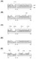
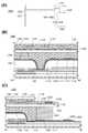
도 1은 반도체 장치를 설명한 상면도.
도 2는 본 발명의 일 형태인 반도체 장치의 제조 방법을 설명한 단면도.
도 3은 본 발명의 일 형태인 반도체 장치의 제조 방법을 설명한 단면도.
도 4는 본 발명의 일 형태인 반도체 장치의 제조 방법을 설명한 단면도.
도 5는 본 발명의 일 형태인 반도체 장치의 제조 방법을 설명한 단면도.
도 6은 본 발명의 일 형태인 반도체 장치의 제조 방법을 설명한 단면도.
도 7은 본 발명의 일 형태인 반도체 장치의 제조 방법을 설명한 단면도.
도 8은 본 발명의 일 형태인 반도체 장치의 제조 방법을 설명한 단면도.
도 9는 본 발명의 일 형태인 반도체 장치의 제조 방법을 설명한 단면도.
도 10은 본 발명의 일 형태인 반도체 장치의 제조 방법을 설명한 단면도.
도 11은 본 발명의 일 형태인 반도체 장치의 제조 방법을 설명한 단면도.
도 12는 본 발명의 일 형태인 반도체 장치의 제조 방법을 설명한 단면도.
도 13은 액정 표시 장치를 설명한 도면.
도 14는 전자 기기를 설명한 도면.
도 15는 본 발명의 일 형태인 반도체 장치의 제조 방법을 설명한 단면도.1 is a top view illustrating a semiconductor device.
2 is a cross-sectional view illustrating a method of manufacturing a semiconductor device according to an embodiment of the present invention.
3 is a cross-sectional view illustrating a method of manufacturing a semiconductor device according to an embodiment of the present invention.
4 is a cross-sectional view illustrating a method of manufacturing a semiconductor device according to an embodiment of the present invention.
5 is a cross-sectional view illustrating a method of manufacturing a semiconductor device according to an embodiment of the present invention.
6 is a cross-sectional view illustrating a method of manufacturing a semiconductor device according to an embodiment of the present invention.
7 is a cross-sectional view illustrating a method of manufacturing a semiconductor device according to an embodiment of the present invention.
8 is a cross-sectional view illustrating a method of manufacturing a semiconductor device according to an embodiment of the present invention.
9 is a cross-sectional view illustrating a method of manufacturing a semiconductor device according to an embodiment of the present invention.
10 is a cross-sectional view illustrating a method of manufacturing a semiconductor device according to an embodiment of the present invention.
11 is a cross-sectional view illustrating a method of manufacturing a semiconductor device according to an embodiment of the present invention.
12 is a cross-sectional view illustrating a method of manufacturing a semiconductor device according to an embodiment of the present invention.
13 is a diagram illustrating a liquid crystal display device.
14 is a diagram illustrating an electronic device.
15 is a cross-sectional view illustrating a method of manufacturing a semiconductor device according to an embodiment of the present invention.
이하에서는, 본 발명의 실시형태에 대하여 도면을 사용하여 자세히 설명한다. 다만, 본 발명은 이하의 설명에 한정되지 않고, 그 형태 및 자세한 사항을 다양하게 변경할 수 있다는 것은 당업자라면 용이하게 이해된다. 또한, 본 발명은 이하에 기재된 실시형태의 내용에 한정되어 해석되는 것이 아니다. 또한, 도면을 사용하여 발명의 구성을 설명함에 있어서, 같은 것을 가리키는 부호는 다른 도면간에서도 공통적으로 사용한다. 또한, 같은 것을 가리킬 때 해치 패턴을 같게 하고 특별히 부호를 붙이지 않은 경우가 있다.Hereinafter, embodiments of the present invention will be described in detail with reference to the drawings. However, it is easily understood by those skilled in the art that the present invention is not limited to the following description, and that the form and details can be variously changed. In addition, this invention is limited to the content of the embodiment described below and is not interpreted. In addition, in describing the configuration of the invention using the drawings, reference numerals indicating the same are used in common among different drawings. In addition, when referring to the same thing, the hatch pattern is made the same and there are cases where no special symbol is attached.
또한, 본 명세서 등에서 제 1 또는 제 2 등으로 부여되는 서수사는 편의상 사용하는 것으로, 공정 순서 또는 적층 순서를 나타내는 것은 아니다. 따라서, 예를 들어 '제 1'을 '제 2' 또는 '제 3' 등으로 적절히 바꿔서 설명할 수 있다. 또한, 본 명세서 등에 기재되어 있는 서수사와, 본 발명의 일 형태를 특정하기 위하여 사용되는 서수사는 일치하지 않은 경우가 있다.In addition, ordinal numbers given as first or second in this specification and the like are used for convenience and do not indicate a process order or a stacking order. Therefore, for example,'first' can be appropriately replaced with'second' or'third', and the like. In addition, the ordinal numbers described in this specification and the like may not coincide with the ordinal numbers used to specify one embodiment of the present invention.
또한, 본 명세서 등에서 "위"라는 용어는 구성 요소의 위치 관계를 "바로 위"에 있는 것으로 한정하는 것은 아니다. 예를 들어, "절연층 위의 게이트 전극"의 표현은, 절연층과 게이트 전극 사이에 다른 구성 요소를 포함하는 것을 제외하지 않는다. "아래"에 대해서도 마찬가지이다. 또한, 평면적으로 보아, 중첩이 없는 경우(중첩되지 않는 경우라고 불러도 좋음)도 제외하지 않는다.In addition, in this specification and the like, the term "above" does not limit the positional relationship of the constituent elements to be "right above". For example, the expression "gate electrode over an insulating layer" does not exclude the inclusion of other components between the insulating layer and the gate electrode. The same is true for "below". In addition, in a plan view, the case where there is no overlap (it may be called a case where it is not overlapped) is also not excluded.
또한, 본 명세서 등에서, "전극" 및 "배선"과 같은 용어는 이들 구성 요소의 기능들을 제한하지는 않는다. 예를 들어, "전극"은 "배선"의 일부로서 사용되는 경우가 있고, 그 반대도 마찬가지이다. "전극" 및 "배선"과 같은 용어는 복수의 "전극"이나 "배선"이 일체가 되어 형성되어 있는 경우 등도 포함한다.Further, in this specification and the like, terms such as "electrode" and "wiring" do not limit the functions of these components. For example, "electrode" is sometimes used as part of "wiring" and vice versa. Terms such as "electrode" and "wiring" also include a case in which a plurality of "electrodes" or "wiring" are formed integrally.
또한, "소스"나 "드레인"의 기능은 다른 극성의 트랜지스터를 채용하는 경우나, 회로 동작에 있어서 전류의 방향이 변화되는 경우 등에는 교체될 수 있다. 따라서, 본 명세서에서, "소스"나 "드레인"이란 용어는 교체하여 사용할 수 있는 것으로 한다.In addition, the functions of "source" and "drain" can be replaced when transistors of different polarities are employed, when the direction of current is changed in circuit operation. Accordingly, in the present specification, the terms "source" and "drain" can be used interchangeably.
또한, "전기적으로 접속"이라는 표현에는 "어떠한 전기적 작용을 갖는 것"을 통하여 접속되어 있는 경우가 포함된다. 여기서, "어떠한 전기적 작용을 갖는 것"은 접속 대상간에서 전기 신호의 주고 받음을 가능하게 하는 것이면 특별한 제한을 받지 않는다. 예를 들어, "어떠한 전기적 작용을 갖는 것"에는, 전극이나 배선 등이 포함된다.In addition, the expression "electrically connected" includes the case of being connected through "having some electrical action". Here, "having any electrical action" is not subject to any particular limitation as long as it enables the exchange of electrical signals between the objects to be connected. For example, "having some electrical action" includes electrodes, wiring, and the like.
또한, "반도체"라고 표기하였을 때에도, 예를 들어 도전성이 충분히 낮은 경우에는 "절연체"로서의 특성을 갖는 경우가 있다. 또한, "반도체"와 "절연체"는 그 경계가 애매하며 엄밀하게 구별할 수 없는 경우가 있다. 따라서, 본 명세서에 기재된 "반도체"는 "절연체"로 바꿔 말할 수 있는 경우가 있다. 마찬가지로, 본 명세서에 기재된 "절연체"는 "반도체"로 바꿔 말할 수 있는 경우가 있다.In addition, even when expressed as "semiconductor", for example, when the conductivity is sufficiently low, it may have properties as "insulator". In addition, the boundary between "semiconductor" and "insulator" is ambiguous and may not be strictly distinguished. Therefore, the "semiconductor" described in the present specification may be referred to as "insulator" in some cases. Likewise, the "insulator" described in the present specification may be referred to as "semiconductor" in some cases.
또한, "반도체"라고 표기하였을 때에도 예를 들어 도전성이 충분히 높은 경우에는 "도전체"로서의 특성을 갖는 경우가 있다. 또한, "반도체"와 "도전체"는 경계가 애매하며 엄밀하게 구별할 수 없는 경우가 있다. 따라서, 본 명세서에 기재된 "반도체"는 "도전체"로 바꿔 말할 수 있는 경우가 있다. 마찬가지로, 본 명세서에 기재된 "도전체"는 "반도체"로 바꿔 말할 수 있는 경우가 있다.In addition, even when expressed as "semiconductor", for example, when the conductivity is sufficiently high, it may have properties as "conductor". In addition, there are cases where the boundary between “semiconductor” and “conductor” is ambiguous and cannot be strictly distinguished. Therefore, the "semiconductor" described in the present specification may be sometimes referred to as "conductor". Similarly, the "conductor" described in the present specification may be sometimes referred to as "semiconductor".
또한, 본 명세서 등에서 "평행"이란, 2개의 직선이 -10° 이상 10° 이하의 각도로 배치되는 상태를 말한다. 따라서, -5° 이상 5° 이하의 경우도 그 범주에 포함된다. 또한, "수직"이란, 2개의 직선이 80° 이상 100° 이하의 각도로 배치된 상태를 말한다. 따라서, 85° 이상 95° 이하의 경우도 그 범주에 포함된다.In addition, in this specification and the like, "parallel" refers to a state in which two straight lines are arranged at an angle of -10° or more and 10° or less. Therefore, cases of -5° or more and 5° or less are included in the category. In addition, "vertical" means a state in which two straight lines are arranged at an angle of 80° or more and 100° or less. Therefore, cases of 85° or more and 95° or less are also included in the category.
또한, 본 명세서 등에 있어서, 삼방정 또는 능면체정은 육방정계에 포함된다.In addition, in this specification and the like, a trigonal crystal or rhombohedral crystal is included in a hexagonal system.
(실시형태 1)(Embodiment 1)
본 발명의 일 형태인 반도체 장치의 제조 방법에 대하여 도 1∼도 10을 사용하여 설명한다. 도 1은 반도체 장치의 상면도이고, 도 1의 (A)에는 액정 표시 장치의 화소 영역으로서 기능할 수 있는 부분, 도 1의 (B) 및 (C)에는 액정 표시 장치의 드라이버 등이 제공된 주변부로서 기능할 수 있는 부분을 도시하였다. 도면의 간략화를 위하여 구성 요소의 일부를 발췌하여 도시하였으며, 예를 들어 후술하는 절연막(104), 절연막(108) 등은 도시하지 않았다. 도 1의 (A) 중 일점 쇄선 X1-X2부분의 단면 구조를 도 2∼도 10의 단면 X1-X2에 도시하였다. 단면 X1-X2는 트랜지스터가 형성되는 영역의 일부의 단면 구조이다. 도 1의 (B) 중 일점 쇄선 Y1-Y2부분의 단면 구조를 도 2∼도 10의 단면 Y1-Y2에 도시하였다. 단면 Y1-Y2는 반도체막 아래에 제공된 도전막과 반도체막 위에 제공된 도전막이 전기적으로 접속되는 영역의 일부의 단면 구조이다.A method of manufacturing a semiconductor device according to an embodiment of the present invention will be described with reference to FIGS. 1 to 10. Fig. 1 is a top view of a semiconductor device, Fig. 1(A) shows a part that can function as a pixel area of a liquid crystal display, and Figs. 1(B) and (C) show a peripheral part provided with a driver, etc. of the liquid crystal display. A part that can function as is shown. In order to simplify the drawing, some of the constituent elements are extracted and illustrated, and for example, the insulating
≪제조 방법 1≫≪Manufacturing method 1≫
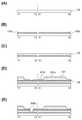
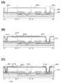
우선, 도 2 및 도 3을 사용하여 도 3의 (D)에 도시된 트랜지스터(150) 및 접속부(160)를 형성하는 방법을 설명한다.First, a method of forming the
<기판><Substrate>
우선, 기판(100)을 준비한다(도 2의 (A) 참조). 기판(100)의 재질 등에 큰 제한은 없지만, 적어도 나중의 가열 처리에 견딜 수 있을 정도로 내열성을 갖는 재료를 사용한다. 예를 들어, 유리 기판, 세라믹 기판, 석영 기판, 사파이어 기판, YSZ(이트리아 안정화 지르코니아) 기판 등을 기판(100)으로서 사용하여도 좋다. 또한, 실리콘이나 탄소화 실리콘 등으로 이루어진 단결정 반도체 기판이나 다결정 반도체 기판, 실리콘 게르마늄 등으로 이루어진 화합물 반도체 기판, SOI 기판 등을 적용할 수도 있다.First, a
또한, 반도체 기판이나 SOI 기판 위에 반도체 소자가 제공된 것을 기판(100)으로서 사용하여도 좋다. 이 경우, 기판(100) 위에, 층간 절연층을 개재(介在)하여 트랜지스터(150)를 형성한다. 이 때, 트랜지스터(150)의 도전막(102b), 도전막(114b), 및 도전막(114c) 중 적어도 하나가, 층간 절연층에 매립된 접속 전극에 의하여 상기 반도체 소자와 전기적으로 접속되는 구성으로 하면 좋다. 반도체 소자 위에 층간 절연층을 개재하여 트랜지스터(150)를 제공함으로써 트랜지스터(150)의 부가로 인한 면적 증가를 억제할 수 있다.Further, a semiconductor substrate or an SOI substrate provided with a semiconductor element may be used as the
또한, 기판(100)으로서 플라스틱 등의 가요성 기판을 사용하고 이 가요성 기판 위에 트랜지스터(150)를 직접 형성하여도 좋다. 또는, 기판(100)과 트랜지스터(150) 사이에 박리층을 제공하여도 좋다. 박리층은, 그 위에 트랜지스터의 일부 또는 전부를 형성하고 나서 기판(100)으로부터 분리하여 다른 기판에 전재(轉載)하기 위하여 사용할 수 있다. 이 결과, 트랜지스터(150)는 내열성이 낮은 기판이나 가요성 기판에도 전재할 수 있다.Further, a flexible substrate such as plastic may be used as the
<도전막 형성><Formation of conductive film>
다음에, 기판(100) 위에 스퍼터링법, CVD법, 증착법 등으로 도전막을 형성하고, 상기 도전막 위에 포토리소그래피 공정으로 레지스트 마스크를 형성한다. 그 다음에, 상기 레지스트 마스크를 사용하여 도전막의 일부를 에칭하여 도전막(102a) 및 도전막(102b)을 형성한다(도 3의 (B) 참조). 도전막(102b)은 트랜지스터(150)에서 게이트 전극으로서 기능할 수 있다.Next, a conductive film is formed on the
도전막(102a) 및 도전막(102b)은 알루미늄, 크로뮴, 구리, 탄탈럼, 티타늄, 몰리브덴, 텅스텐 중에서 선택된 금속 또는 상술한 금속을 성분으로 하는 합금, 또는 상술한 금속을 조합한 합금 등을 사용하여 형성할 수 있다. 또한, 망가니즈, 지르코늄 중 어느 하나 또는 복수 중에서 선택된 금속을 사용하여도 좋다.The
또한, 도전막(102a) 및 도전막(102b)은 단층 구조라도 좋고, 2층 이상의 적층 구조라도 좋다. 예를 들어, 알루미늄막의 위 또는 아래에 텅스텐, 티타늄, 몰리브덴 중에서 선택된 금속, 또는 상술한 금속을 성분으로 하는 합금 등의, 배리어막으로서 기능하는 막을 적층하는 2층 구조로 하여도 좋다. 또한, 알루미늄막의 상하에 상술한 배리어막으로서 기능하는 막을 적층하는 3층 구조로 하여도 좋다. 이와 마찬가지로, 구리막의 위 또는 아래에 상술한 배리어막으로서 기능하는 막을 적층하는 2층 구조로 하여도 좋다. 또한, 구리막의 상하에 상술한 배리어막으로서 기능하는 막을 적층하는 3층 구조로 하여도 좋다.Further, the
알루미늄막 및 구리막은 저항이 낮으므로, 도전막(102a) 및 도전막(102b)에 사용함으로써 반도체 장치의 소비 전력을 삭감할 수 있다. 또한, 텅스텐막, 티타늄막, 몰리브덴막 등 배리어막으로서 기능하는 막을 알루미늄막 또는 구리막 등과 접촉하여 적층시킴으로써 알루미늄이나 구리의 확산을 억제하여 반도체 장치의 신뢰성을 향상시킬 수 있다.Since the aluminum film and the copper film have low resistance, power consumption of the semiconductor device can be reduced by using it for the
또한, 도전막(102b)과 후술하는 절연막(104) 사이에 In-Ga-Zn계 산화질화물 반도체막, In-Sn계 산화질화물 반도체막, In-Ga계 산화질화물 반도체막, In-Zn계 산화질화물 반도체막, Sn계 산화질화물 반도체막, In계 산화질화물 반도체막, 금속 질화막(InN, ZnN 등) 등을 제공하여도 좋다. 이들 막은 5eV 이상, 바람직하게는 5.5eV 이상의 일함수를 가지며, 이것은 산화물 반도체의 전자 친화력보다 큰 값이므로, 후술하는 반도체막에 산화물 반도체를 사용하는 경우 트랜지스터의 문턱 전압을 플러스로 시프트할 수 있으며 소위 노멀리 오프 특성의 스위칭 소자를 실현할 수 있다. 예를 들어, In-Ga-Zn계 산화질화물 반도체막을 사용하는 경우, 적어도 반도체막(106b)보다 높은 질소 농도, 구체적으로는 질소 농도가 7atom% 이상의 In-Ga-Zn계 산화질화물 반도체막을 사용한다.In addition, an In-Ga-Zn-based oxynitride semiconductor film, an In-Sn-based oxynitride semiconductor film, an In-Ga-based oxynitride semiconductor film, and In-Zn-based oxidation between the
<절연막 형성><Insulation film formation>
다음에, 기판(100), 도전막(102a) 및 도전막(102b) 위에 절연막(104)을 형성한다(도 2의 (C) 참조). 절연막(104)은 트랜지스터(150)에서 게이트 절연막으로서 기능할 수 있다.Next, an insulating
절연막(104)은 예를 들어, 산화 실리콘, 산화질화 실리콘, 질화산화 실리콘, 질화 실리콘, 산화 알루미늄, 산화 하프늄, 산화 갈륨 또는 Ga-Zn계 금속 산화물 등을 사용하면 좋고, 적층 또는 단층으로 제공한다.The insulating
또한, 절연막(104)으로서, 하프늄 실리케이트(HfSiOx), 질소가 첨가된 하프늄 실리케이트(HfSixOyNz), 질소가 첨가된 하프늄 알루미네이트(HfAlxOyNz), 산화 하프늄, 산화 이트륨 등의 high-k 재료를 사용함으로써 트랜지스터의 게이트 누설을 저감시킬 수 있다.In addition, as the insulating
절연막(104)은 스퍼터링법, CVD법, 증착법 등으로 형성한다.The insulating
절연막(104)으로서 질화 실리콘막을 형성하는 경우, 2단계의 형성 방법을 이용하는 것이 바람직하다. 우선, 실레인, 질소, 및 암모니아의 혼합 가스를 원료 가스로서 사용한 플라즈마 CVD법에 의하여, 결함이 적은 제 1 질화 실리콘막을 형성한다. 다음에, 원료 가스를, 실레인 및 질소의 혼합 가스로 스위칭하여, 수소 농도가 낮고, 또한 수소를 블로킹하는 것이 가능한 제 2 질화 실리콘막을 형성한다. 이러한 형성 방법에 의하여, 절연막(104)으로서, 결함이 적고, 또한 수소 블로킹성을 갖는 질화 실리콘막을 형성할 수 있다.When forming the silicon nitride film as the insulating
또한, 절연막(104)으로서 산화 갈륨막을 형성하는 경우, MOCVD(Metal Organic Chemical Vapor Deposition)법을 이용하여 형성할 수 있다.Further, when a gallium oxide film is formed as the insulating
<반도체막 형성><Semiconductor film formation>
다음에 스퍼터링법, CVD법, 증착법 등으로 절연막(104) 위에 반도체막을 형성하고, 상기 반도체막 위에 포토리소그래피 공정으로 레지스트 마스크를 형성한다. 그 다음에, 상기 레지스트 마스크를 사용하여 반도체막의 적어도 일부를 에칭하여 반도체막(106a) 및 반도체막(106b)을 형성한다(도 2의 (D) 참조). 반도체막(106b)은 트랜지스터(150)의 채널 영역을 포함한다.Next, a semiconductor film is formed on the insulating
반도체막(106a) 및 반도체막(106b)에는 다양한 반도체 재료를 사용할 수 있다. 구체적으로는, 비정질 실리콘, 미결정 실리콘, 다결정 실리콘, 단결정 실리콘 등을 사용할 수 있고, 이들의 막을 단층 또는 적층으로 제공할 수 있다. 또한, 이들 반도체막의 일부 또는 이들 반도체막을 적층한 경우에는 적어도 하나의 층에, 도전형을 부여하는 불순물을 첨가하여도 좋다.Various semiconductor materials can be used for the
또한, 상기 반도체 재료 외에 산화물 반도체를 사용할 수 있다. 산화물 반도체를 사용한 트랜지스터에는, 오프 전류가 매우 낮은 특성을 갖는 것이 있다. 상기 트랜지스터를 사용하면 액정 표시 장치에서의 각 화소의 용량 소자에 입력된 신호의 유지 능력이 높게 되어, 예를 들어 정지 화상 표시 등에서 프레임 주파수를 작게 할 수 있다. 프레임 주파수를 작게 함으로써 표시 장치의 소비 전력을 저감시킬 수 있다.In addition, oxide semiconductors may be used in addition to the above semiconductor materials. Some transistors using oxide semiconductors have very low off-current characteristics. When the transistor is used, the ability to hold a signal input to the capacitive element of each pixel in the liquid crystal display device is increased, and the frame frequency can be reduced in, for example, still image display. By reducing the frame frequency, power consumption of the display device can be reduced.
이하에서, 반도체막(106a) 및 반도체막(106b)에 적용할 수 있는 산화물 반도체에 대하여 설명한다.Hereinafter, an oxide semiconductor applicable to the
산화물 반도체는 예를 들어 인듐을 포함한다. 인듐을 포함한 산화물 반도체는 캐리어 이동도(전자 이동도)가 높게 된다. 또한, 산화물 반도체는 원소 M을 포함하면 바람직하다. 원소 M으로서는, 예를 들어 알루미늄, 갈륨, 이트륨, 또는 주석 등이 있다. 원소 M은, 예를 들어 산소와의 결합 에너지가 높은 원소이다. 원소 M은 예를 들어 산화물 반도체의 에너지 갭을 크게 하는 기능을 갖는 원소이다. 또한, 산화물 반도체는 아연을 포함하면 바람직하다. 산화물 반도체가 아연을 포함하면, 결정질의 산화물 반도체가 되기 쉽다. 또한, 산화물 반도체의 가전자대 상단의 에너지(Ev)는 예를 들어 아연의 원자수 비율에 의하여 제어할 수 있는 경우가 있다.Oxide semiconductors include, for example, indium. An oxide semiconductor containing indium has a high carrier mobility (electron mobility). In addition, it is preferable that the oxide semiconductor contains the element M. Examples of the element M include aluminum, gallium, yttrium, or tin. The element M is, for example, an element having high binding energy with oxygen. Element M is an element having a function of increasing the energy gap of an oxide semiconductor, for example. In addition, it is preferable that the oxide semiconductor contains zinc. When the oxide semiconductor contains zinc, it tends to become a crystalline oxide semiconductor. In addition, the energy (Ev) of the upper valence band of the oxide semiconductor can be controlled by, for example, the ratio of the number of zinc atoms in some cases.
다만, 산화물 반도체는 인듐을 포함하지 않아도 좋다. 산화물 반도체는 예를 들어 Zn-Sn 산화물, Ga-Sn 산화물이라도 좋다.However, the oxide semiconductor may not contain indium. The oxide semiconductor may be, for example, a Zn-Sn oxide or a Ga-Sn oxide.
또한, 산화물 반도체를, In 및 M의 합을 100atomic%로 하였을 때, In 및 M의 원자수 비율이 In 50atomic% 미만, M 50atomic% 이상, 또는 In 25atomic% 미만, M 75atomic% 이상인 In-M-Zn산화물로 하여도 좋다. 또한, 산화물 반도체를, In 및 M의 합을 100atomic%로 하였을 때, In 및 M의 원자수 비율이 In 25atomic% 이상, M 75atomic% 미만, 또는 In 34atomic% 이상, M 66atomic% 미만인 In-M-Zn산화물로 하여도 좋다.In addition, in the oxide semiconductor, when the sum of In and M is 100 atomic%, the atomic ratio of In and M is less than In 50 atomic%, M 50 atomic% or more, or In 25 atomic% or less, M 75 atomic% or more. Zn oxide may be used. In addition, in the oxide semiconductor, when the sum of In and M is 100 atomic%, the atomic ratio of In and M is In 25 atomic% or more, M 75 atomic% or more, In 34 atomic% or more, M In-M- Zn oxide may be used.
또한, 산화물 반도체는 에너지 갭이 크다. 산화물 반도체의 에너지 갭은 2.7eV 이상 4.9eV 이하, 바람직하게는 3eV 이상 4.7eV 이하, 더 바람직하게는 3.2eV 이상 4.4eV 이하로 한다.In addition, the oxide semiconductor has a large energy gap. The energy gap of the oxide semiconductor is set to be 2.7 eV or more and 4.9 eV or less, preferably 3 eV or more and 4.7 eV or less, and more preferably 3.2 eV or more and 4.4 eV or less.
트랜지스터의 전기 특성을 안정화시키기 위해서는, 산화물 반도체 내의 불순물 농도를 저감시켜 고순도 진성화하는 것이 유효하다. 또한, 산화물 반도체에서 주성분 이외(1atomic% 미만)의 경(輕)원소, 반금속 원소, 금속 원소 등은 불순물이다. 예를 들어, 수소, 리튬, 탄소, 질소, 불소, 나트륨, 실리콘, 염소, 칼륨, 칼슘, 티타늄, 철, 니켈, 구리, 게르마늄, 스트론튬, 지르코늄, 및 하프늄은 산화물 반도체 내에서 불순물이 되는 경우가 있다. 따라서, 산화물 반도체에 근접하는 막 내의 불순물 농도도 저감시키는 것이 바람직하다.In order to stabilize the electrical characteristics of the transistor, it is effective to reduce the concentration of impurities in the oxide semiconductor to achieve high purity. In addition, in the oxide semiconductor, light elements, semimetal elements, metal elements, etc. other than the main component (less than 1 atomic%) are impurities. For example, hydrogen, lithium, carbon, nitrogen, fluorine, sodium, silicon, chlorine, potassium, calcium, titanium, iron, nickel, copper, germanium, strontium, zirconium, and hafnium are sometimes impurities in oxide semiconductors. have. Therefore, it is desirable to also reduce the impurity concentration in the film adjacent to the oxide semiconductor.
예를 들어, 산화물 반도체층 내에 실리콘이 포함되면 불순물 준위를 형성하는 경우가 있다. 또한, 산화물 반도체의 표면에 실리콘이 있으면 불순물 준위를 형성하는 경우가 있다. 그러므로, 산화물 반도체의 내부, 표면의 실리콘 농도는 이차 이온 질량 분석법(SIMS: Secondary Ion Mass Spectrometry)에서, 1×10¹⁹atoms/cm3 미만, 바람직하게는 5×10¹⁸atoms/cm3 미만, 더 바람직하게는 2×10¹⁸atoms/cm3 미만으로 한다.For example, if silicon is included in the oxide semiconductor layer, an impurity level may be formed. Further, if silicon is present on the surface of the oxide semiconductor, impurity levels may be formed. Therefore, the silicon concentration on the inside and the surface of the oxide semiconductor is less than 1×10¹⁹ atoms/cm3 , preferably less than 5×10¹⁸ atoms/cm3 , and more in a secondary ion mass spectrometry (SIMS) method. It is preferably less than 2×10¹⁸ atoms/cm3 .
또한, 산화물 반도체 내에서 수소는 불순물 준위를 형성하고 캐리어 밀도를 증대시키는 경우가 있다. 그러므로, SIMS에 의한 산화물 반도체의 수소 농도는, 2×10²⁰atoms/cm3 이하, 바람직하게는 5×10¹⁹atoms/cm3 이하, 더 바람직하게는 1×10¹⁹atoms/cm3 이하, 더욱 바람직하게는 5×10¹⁸atoms/cm3 이하로 한다. 또한, 산화물 반도체 내에서 질소는 불순물 준위를 형성하고 캐리어 밀도를 증대시키는 경우가 있다. 그러므로, SIMS에 의한 산화물 반도체 내의 질소 농도는, 5×10¹⁹atoms/cm3 미만, 바람직하게는 5×10¹⁸atoms/cm3 이하, 더 바람직하게는 1×10¹⁸atoms/cm3 이하, 더욱 바람직하게는 5×10¹⁷atoms/cm3 이하로 한다.In addition, in the oxide semiconductor, hydrogen may form an impurity level and increase the carrier density. Therefore, the hydrogen concentration of the oxide semiconductor by SIMS is 2×10²⁰ atoms/cm3 or less, preferably 5×10¹⁹ atoms/cm3 or less, more preferably 1×10¹⁹ atoms/cm3 or less, furthermore Preferably it is 5×10¹⁸ atoms/cm3 or less. In addition, in the oxide semiconductor, nitrogen sometimes forms an impurity level and increases the carrier density. Therefore, the nitrogen concentration in the oxide semiconductor by SIMS is less than 5×10¹⁹ atoms/cm3 , preferably 5×10¹⁸ atoms/cm3 or less, more preferably 1×10¹⁸ atoms/cm3 or less, and further Preferably it is 5×10¹⁷ atoms/cm3 or less.
산화물 반도체막은 비단결정 산화물 반도체막과 단결정 산화물 반도체막으로 대별된다. 비단결정 산화물 반도체막이란, CAAC-OS(C-Axis Aligned Crystalline Oxide Semiconductor)막, 다결정 산화물 반도체막, 미결정 산화물 반도체막, 비정질 산화물 반도체막 등을 가리킨다.The oxide semiconductor film is roughly classified into a non-single crystal oxide semiconductor film and a single crystal oxide semiconductor film. The non-single crystal oxide semiconductor film refers to a CAAC-OS (C-Axis Aligned Crystalline Oxide Semiconductor) film, a polycrystalline oxide semiconductor film, a microcrystalline oxide semiconductor film, an amorphous oxide semiconductor film, and the like.
산화물 반도체막은, 예를 들어 CAAC-OS막을 가져도 좋다. 우선, CAAC-OS막에 대하여 설명한다.The oxide semiconductor film may have a CAAC-OS film, for example. First, the CAAC-OS film will be described.
CAAC-OS막은 복수의 결정부를 갖는 산화물 반도체막의 하나이며, 결정부의 대부분은 한 변이 100nm 미만인 입방체 내에 들어가는 사이즈이다. 따라서, CAAC-OS막에 포함되는 결정부는 한 변이 10nm 미만, 5nm 미만, 또는 3nm 미만인 입방체 내에 들어가는 사이즈인 경우도 포함된다.The CAAC-OS film is one of oxide semiconductor films having a plurality of crystal portions, and most of the crystal portions are sized to fit in a cube whose one side is less than 100 nm. Accordingly, the case where the crystal part included in the CAAC-OS film has a size that fits in a cube whose one side is less than 10 nm, less than 5 nm, or less than 3 nm is also included.
CAAC-OS막을 투과형 전자 현미경(TEM: Transmission Electron Microscope)에 의하여 관찰하면, 결정부와 결정부의 명확한 경계, 즉 결정 입계(그레인 바운더리라고도 함)는 확인되지 않는다. 따라서, CAAC-OS막은 결정 입계에 기인하는 전자 이동도의 저하가 일어나기 어렵다고 할 수 있다.When the CAAC-OS film is observed with a Transmission Electron Microscope (TEM), a clear boundary between the crystal part and the crystal part, that is, the grain boundary (also referred to as grain boundary) is not confirmed. Therefore, it can be said that the CAAC-OS film is unlikely to cause a decrease in electron mobility due to grain boundaries.
CAAC-OS막을 시료면에 대략 평행한 방향으로부터 TEM에 의하여 관찰(단면 TEM 관찰)하면, 결정부에서 금속 원자가 층상으로 배열되어 있는 것을 확인할 수 있다. 금속 원자의 각 층은 CAAC-OS막을 형성하는 면(피형성면이라고도 함) 또는 상면의 요철을 반영한 형상이며, CAAC-OS막의 피형성면 또는 상면과 평행하게 배열된다.When the CAAC-OS film is observed by TEM from a direction substantially parallel to the sample surface (cross-sectional TEM observation), it can be confirmed that metal atoms are arranged in a layered form in the crystal part. Each layer of metal atoms has a shape reflecting the unevenness of the CAAC-OS film forming surface (also referred to as the formation surface) or the upper surface, and is arranged parallel to the formation surface or the upper surface of the CAAC-OS film.
한편, CAAC-OS막을 시료면에 대략 수직인 방향으로부터 TEM에 의하여 관찰(평면 TEM 관찰)하면, 결정부에서 금속 원자가 삼각형 또는 육각형으로 배열되어 있는 것을 확인할 수 있다. 그러나, 상이한 결정부들간에서 금속 원자의 배열에는 규칙성이 보이지 않는다.On the other hand, when the CAAC-OS film is observed by TEM from a direction substantially perpendicular to the sample plane (planar TEM observation), it can be confirmed that metal atoms are arranged in a triangular or hexagonal shape in the crystal part. However, there is no regularity in the arrangement of metal atoms between different crystal parts.
단면 TEM 관찰 및 평면 TEM 관찰로부터, CAAC-OS막의 결정부는 배향성을 갖는 것을 알 수 있다.From cross-sectional TEM observation and planar TEM observation, it can be seen that the crystal portion of the CAAC-OS film has orientation.
CAAC-OS막에 대하여 X선 회절(XRD: X-Ray Diffraction) 장치를 사용하여 구조 해석을 수행하면, 예를 들어 InGaZnO4의 결정을 갖는 CAAC-OS막의 out-of-plane법에 의한 해석에서는, 회절각(2θ)이 31° 근방일 때 피크가 나타나는 경우가 있다. 이 피크는, InGaZnO4의 결정의 (009)면에 귀속되기 때문에, CAAC-OS막의 결정이 c축 배향성을 갖고, c축이 피형성면 또는 상면에 대략 수직인 방향으로 배향하는 것을 확인할 수 있다.When structural analysis is performed using an X-ray diffraction (XRD) device for the CAAC-OS film, for example, in the out-of-plane analysis of the CAAC-OS film having InGaZnO4 crystals, , When the diffraction angle (2θ) is around 31°, a peak may appear. Since this peak is attributed to the (009) plane of the InGaZnO4 crystal, it can be confirmed that the crystal of the CAAC-OS film has c-axis orientation, and the c-axis is oriented in a direction substantially perpendicular to the surface to be formed or the top surface. .
한편, c축에 대략 수직인 방향으로부터 X선을 입사시키는 in-plane법에 의한 CAAC-OS막의 해석에서는, 2θ가 56° 근방일 때 피크가 나타나는 경우가 있다. 이 피크는 InGaZnO4의 결정의 (110)면에 귀속된다. InGaZnO4의 단결정 산화물 반도체막의 경우에는, 2θ를 56° 근방에 고정하고, 시료면의 법선 벡터를 축(φ축)으로 하여 시료를 회전시키면서 분석(φ 스캔)을 수행하면, (110)면과 등가인 결정면에 귀속되는 6개의 피크가 관찰된다. 한편, CAAC-OS막의 경우에는, 2θ를 56° 근방에 고정하고 φ 스캔을 수행하여도 명료한 피크가 나타나지 않는다.On the other hand, in analysis of the CAAC-OS film by the in-plane method in which X-rays are incident from a direction substantially perpendicular to the c-axis, a peak may appear when 2θ is around 56°. This peak is attributed to the (110) plane of the InGaZnO4 crystal. In the case of a single crystal oxide semiconductor film of InGaZnO4 , if 2θ is fixed around 56° and the sample is rotated with the normal vector of the sample surface as the axis (φ axis), the analysis (φ scan) is performed. Six peaks attributed to the equivalent crystal plane are observed. On the other hand, in the case of the CAAC-OS film, even if 2θ is fixed around 56° and a φ scan is performed, a clear peak does not appear.
상술한 것으로부터, CAAC-OS막에 있어서, 상이한 결정부들간에서는 a축 및 b축의 배향이 불규칙하지만, c축 배향성을 가지며 c축이 피형성면 또는 상면의 법선 벡터에 평행한 방향으로 배향하는 것을 알 수 있다. 따라서, 상술한 단면 TEM 관찰로 확인된 층상으로 배열된 금속 원자의 각층은, 결정의 a-b면에 평행한 면이다.From the above, in the CAAC-OS film, the orientation of the a-axis and the b-axis is irregular between different crystal parts, but has c-axis orientation and the c-axis is oriented in a direction parallel to the normal vector of the surface to be formed or the top surface. Can be seen. Therefore, each layer of metal atoms arranged in a layered form confirmed by the cross-sectional TEM observation described above is a plane parallel to the a-b plane of the crystal.
또한, 결정부는 CAAC-OS막을 형성하였을 때 또는 가열 처리 등의 결정화 처리를 수행하였을 때에 형성된다. 상술한 바와 같이, 결정의 c축은 CAAC-OS막의 피형성면 또는 상면의 법선 벡터에 평행한 방향으로 배향한다. 따라서, 예를 들어 CAAC-OS막의 형상을 에칭 등에 의하여 변화시킨 경우, 결정의 c축이 CAAC-OS막의 피형성면 또는 상면의 법선 벡터에 평행하게 배향하지 않을 수도 있다.Further, the crystal portion is formed when the CAAC-OS film is formed or when crystallization treatment such as heat treatment is performed. As described above, the c-axis of the crystal is oriented in a direction parallel to the normal vector of the surface to be formed or the top surface of the CAAC-OS film. Therefore, for example, when the shape of the CAAC-OS film is changed by etching or the like, the c-axis of the crystal may not be oriented parallel to the normal vector of the formation surface or the upper surface of the CAAC-OS film.
또한, CAAC-OS막 내의 결정화도가 균일하지 않아도 좋다. 예를 들어, CAAC-OS막의 결정부가 CAAC-OS막의 상면 근방으로부터의 결정 성장에 의하여 형성되는 경우에는, 상면 근방의 영역은 피형성면 근방의 영역보다 결정화도가 높게 되는 경우가 있다. 또한, CAAC-OS막에 불순물을 첨가하는 경우에는, 불순물이 첨가된 영역의 결정화도가 변화되어, 부분적으로 결정화도가 상이한 영역이 형성될 수도 있다.Further, the crystallinity in the CAAC-OS film may not be uniform. For example, when the crystal part of the CAAC-OS film is formed by crystal growth from the vicinity of the upper surface of the CAAC-OS film, the crystallinity of the region near the upper surface may be higher than that of the region near the surface to be formed. Further, when an impurity is added to the CAAC-OS film, the crystallinity of the region to which the impurity is added is changed, so that a region having a partially different crystallinity may be formed.
또한, InGaZnO4의 결정을 갖는 CAAC-OS막의 out-of-plane법에 의한 해석에서는, 2θ가 31° 근방일 때의 피크에 더하여, 2θ가 36° 근방일 때의 피크도 나타나는 경우가 있다. 2θ가 36° 근방일 때의 피크는 CAAC-OS막 내의 일부에, c축 배향성을 갖지 않는 결정이 포함되는 것을 가리킨다. CAAC-OS막은 2θ가 31° 근방일 때 피크가 나타나고, 2θ가 36° 근방일 때 피크가 나타나지 않는 것이 바람직하다.In addition, in the analysis by the out-of-plane method of the CAAC-OS film having InGaZnO4 crystals, in addition to the peak when 2θ is around 31°, a peak when 2θ is around 36° may also appear. The peak when 2θ is around 36° indicates that a crystal having no c-axis alignment is contained in a part of the CAAC-OS film. In the CAAC-OS film, it is preferable that a peak appears when 2θ is around 31° and no peak appears when 2θ is around 36°.
CAAC-OS막은 불순물 농도가 낮은 산화물 반도체막이다. 불순물은 수소, 탄소, 실리콘, 전이 금속 원소 등 산화물 반도체막의 주성분 이외의 원소이다. 특히 산화물 반도체막을 구성하는 금속 원소보다 산소와의 결합력이 강한 실리콘 등의 원소는, 산화물 반도체막에서 산소를 빼앗음으로써 산화물 반도체막의 원자 배열을 흐트러지게 하고 결정성을 저하시키는 요인이 된다. 또한 철이나 니켈 등의 중금속, 아르곤, 이산화탄소 등은 원자 반경(또는 분자 반경)이 크기 때문에 산화물 반도체막 내부에 포함되면 산화물 반도체막의 원자 배열을 흐트러지게 하고 결정성을 저하시키는 요인이 된다. 또한, 산화물 반도체막에 포함되는 불순물은 캐리어 트랩이나 캐리어 발생원이 되는 경우가 있다.The CAAC-OS film is an oxide semiconductor film having a low impurity concentration. Impurities are elements other than the main components of the oxide semiconductor film, such as hydrogen, carbon, silicon, and transition metal elements. In particular, an element such as silicon, which has a stronger binding force with oxygen than a metal element constituting the oxide semiconductor film, deprives oxygen from the oxide semiconductor film, thereby disrupting the atomic arrangement of the oxide semiconductor film and deteriorating crystallinity. In addition, heavy metals such as iron and nickel, argon, carbon dioxide, and the like have a large atomic radius (or molecular radius), and thus, when included in the oxide semiconductor film, the atomic arrangement of the oxide semiconductor film is disturbed and crystallinity is deteriorated. In addition, impurities contained in the oxide semiconductor film may become carrier traps or carrier generation sources.
또한 CAAC-OS막은 결함 준위 밀도가 낮은 산화물 반도체막이다. 예를 들어 산화물 반도체막 내의 산소 결손은 캐리어 트랩이 되거나 또는 수소를 포획함으로써 캐리어 발생원이 되는 경우가 있다.Further, the CAAC-OS film is an oxide semiconductor film having a low density of defect states. For example, oxygen vacancies in the oxide semiconductor film may become carrier traps or become carrier generation sources by trapping hydrogen.
불순물 농도가 낮으며 결함 준위 밀도가 낮은(산소 결손이 적은) 것을 고순도 진성 또는 실질적으로 고순도 진성이라고 부른다. 고순도 진성 또는 실질적으로 고순도 진성인 산화물 반도체막은 캐리어 발생원이 적어 캐리어 밀도가 낮게 된다. 따라서, 상기 산화물 반도체막을 사용한 트랜지스터는 문턱 전압이 마이너스가 되는 전기 특성(노멀리 온이라고도 함)을 갖게 되는 경우가 적다. 또한, 고순도 진성 또는 실질적으로 고순도 진성인 산화물 반도체막은 캐리어 트랩이 적다. 따라서, 상기 산화물 반도체막을 사용한 트랜지스터는 전기 특성의 변동이 작고 신뢰성이 높은 트랜지스터가 된다. 또한, 산화물 반도체막의 캐리어 트랩에 포획된 전하는 방출될 때까지 걸리는 시간이 길어 마치 고정 전하처럼 행동하는 경우가 있다. 그러므로 불순물 농도가 높으며 결함 준위 밀도가 높은 산화물 반도체막을 사용한 트랜지스터는 전기 특성이 불안정하게 되는 경우가 있다.A low impurity concentration and a low density of defect states (less oxygen defects) are called high-purity intrinsic or substantially high-purity intrinsic. The high-purity intrinsic or substantially high-purity intrinsic oxide semiconductor film has few carrier generation sources, resulting in a low carrier density. Accordingly, the transistor using the oxide semiconductor film is less likely to have an electrical characteristic (also referred to as normally on) in which the threshold voltage is negative. In addition, the high-purity intrinsic or substantially high-purity intrinsic oxide semiconductor film has few carrier traps. Accordingly, a transistor using the oxide semiconductor film has a small variation in electrical characteristics and a high reliability transistor. In addition, the charge trapped in the carrier trap of the oxide semiconductor film takes a long time to be discharged, so it may act like a fixed charge. Therefore, a transistor using an oxide semiconductor film having a high impurity concentration and a high density of defect states may have unstable electrical characteristics.
또한, CAAC-OS막을 사용한 트랜지스터는 가시광이나 자외광의 조사에 기인한 전기 특성의 변동이 작다.In addition, a transistor using a CAAC-OS film exhibits little variation in electrical characteristics due to irradiation of visible light or ultraviolet light.
다음에, 미결정 산화물 반도체막에 대하여 설명한다.Next, the microcrystalline oxide semiconductor film will be described.
미결정 산화물 반도체막은 TEM에 의한 관찰상에서는 결정부를 명확히 확인할 수 없는 경우가 있다. 미결정 산화물 반도체막에 포함되는 결정부는 1nm 이상 100nm 이하, 또는 1nm 이상 10nm 이하의 크기인 경우가 많다. 특히, 1nm 이상 10nm 이하, 또는 1nm 이상 3nm 이하의 미결정인 나노 결정(nc: nanocrystal)을 갖는 산화물 반도체막을 nc-OS(nanocrystalline Oxide Semiconductor)막이라고 부른다. 또한, nc-OS막은 예를 들어 TEM에 의한 관찰상에서는 결정 입계를 명확히 확인할 수 없는 경우가 있다.The microcrystalline oxide semiconductor film may not be able to clearly confirm the crystal part on the observation by TEM. The crystal portion included in the microcrystalline oxide semiconductor film is often 1 nm or more and 100 nm or less, or 1 nm or more and 10 nm or less. In particular, an oxide semiconductor film having a microcrystalline nanocrystal (nc: nanocrystal) of 1 nm or more and 10 nm or less, or 1 nm or more and 3 nm or less is referred to as a nanocrystalline oxide semiconductor (nc-OS) film. In addition, in the nc-OS film, for example, crystal grain boundaries may not be clearly confirmed on an observation by TEM in some cases.
nc-OS막은 미소한 영역(예를 들어 1nm 이상 10nm 이하의 영역, 특히 1nm 이상 3nm 이하의 영역)에서 원자 배열에 주기성을 갖는다. 또한, nc-OS막은 상이한 결정부들간에서 결정 방위에 규칙성이 보이지 않는다. 그러므로, 막 전체에서 배향성을 찾을 수 없다. 따라서, nc-OS막은 분석 방법에 따라서는 비정질 산화물 반도체막과 구별할 수 없는 경우가 있다. 예를 들어 nc-OS막에 대하여 결정부보다 직경이 큰 X선을 사용하는 XRD 장치를 사용하여 구조 해석을 수행하면, out-of-plane법에 의한 해석에서는 결정면을 나타내는 피크가 검출되지 않는다. 또한, nc-OS막에 대하여 결정부보다 직경이 큰(예를 들어 50nm 이상) 전자선을 사용하는 전자선 회절(제한 시야 전자선 회절이라고도 함)을 수행하면 할로 패턴(halo pattern)과 같은 회절 패턴이 관측된다. 한편, nc-OS막에 대하여, 결정부의 크기와 가깝거나 결정부보다 작은 직경(예를 들어 1nm 이상 30nm 이하)의 전자선을 사용하는 전자선 회절(나노 빔 전자선 회절이라고도 함)을 수행하면, 스폿이 관측된다. 또한, nc-OS막에 대하여 나노 빔 전자선 회절을 수행하면, 휘도가 높은 원형(링(ring)형)의 영역이 관측되는 경우가 있다. 또한, nc-OS막에 대하여 나노 빔 전자 회절을 수행한 경우, 링형 영역 내에 복수의 스폿이 관측될 수 있다.The nc-OS film has periodicity in atomic arrangement in a small region (eg, 1 nm or more and 10 nm or less, particularly 1 nm or more and 3 nm or less). In addition, the nc-OS film does not show regularity in the crystal orientation between different crystal portions. Therefore, orientation cannot be found throughout the film. Therefore, the nc-OS film may not be distinguishable from the amorphous oxide semiconductor film depending on the analysis method. For example, when structural analysis is performed using an XRD apparatus using an X-ray having a diameter larger than that of the crystal part for the nc-OS film, the peak indicating the crystal plane is not detected in the analysis by the out-of-plane method. In addition, when electron diffraction (also referred to as limited-field electron diffraction) using an electron beam having a diameter larger than the crystal part (for example, 50 nm or more) is performed on the nc-OS film, a diffraction pattern such as a halo pattern is observed. do. On the other hand, when electron beam diffraction (also referred to as nano-beam electron diffraction) using an electron beam having a diameter close to or smaller than the crystal portion (for example, 1 nm or more and 30 nm or less) is performed on the nc-OS film, the spot Is observed. In addition, when nano-beam electron diffraction is performed on the nc-OS film, a circular (ring-shaped) region with high luminance may be observed. In addition, when nano-beam electron diffraction is performed on the nc-OS film, a plurality of spots may be observed in the ring-shaped region.
nc-OS막은 비정질 산화물 반도체막보다 규칙성이 높은 산화물 반도체막이다. 따라서, nc-OS막은 비정질 산화물 반도체막보다 결함 준위 밀도가 낮다. 다만, nc-OS막에서는 상이한 결정부들간에서 결정 방위에 규칙성이 보이지 않는다. 따라서, nc-OS막은 CAAC-OS막보다 결함 준위 밀도가 높다.The nc-OS film is an oxide semiconductor film having higher regularity than an amorphous oxide semiconductor film. Therefore, the nc-OS film has a lower density of defect states than the amorphous oxide semiconductor film. However, in the nc-OS film, there is no regularity in the crystal orientation between different crystal parts. Therefore, the nc-OS film has a higher density of defect states than the CAAC-OS film.
또한, 산화물 반도체막은 예를 들어 비정질 산화물 반도체막, 미결정 산화물 반도체막, CAAC-OS막 중 2종류 이상을 갖는 적층막이라도 좋다.Further, the oxide semiconductor film may be a laminated film having two or more of an amorphous oxide semiconductor film, a microcrystalline oxide semiconductor film, and a CAAC-OS film, for example.
예를 들어, 산화물 반도체층(S1)과 산화물 반도체층(S2)은, 이 순서대로 형성된 다층막이라도 좋다.For example, the oxide semiconductor layer S1 and the oxide semiconductor layer S2 may be multilayered films formed in this order.
이 경우, 예를 들어 산화물 반도체층(S2)의 전도대 하단의 에너지(Ec)를 산화물 반도체층(S1)보다 높은 것으로 한다. 구체적으로는 산화물 반도체층(S2)으로서는, 전자 친화력이 산화물 반도체층(S1)보다 0.07eV 이상 1.3eV 이하, 바람직하게는 0.1eV 이상 0.7eV 이하, 더 바람직하게는 0.15eV 이상 0.4eV 이하 작은 산화물 반도체를 사용한다. 또한, 전자 친화력은 진공 준위와 전도대 하단의 에너지 차이이다.In this case, for example, the energy Ec at the lower end of the conduction band of the oxide semiconductor layer S2 is assumed to be higher than that of the oxide semiconductor layer S1. Specifically, as the oxide semiconductor layer S2, an oxide having an electron affinity of 0.07 eV or more and 1.3 eV or less, preferably 0.1 eV or more and 0.7 eV or less, more preferably 0.15 eV or more and 0.4 eV or less than the oxide semiconductor layer S1. Use a semiconductor. In addition, electron affinity is the difference between the energy of the vacuum level and the conduction band.
또는, 예를 들어 산화물 반도체층(S2)의 에너지 갭을 산화물 반도체층(S1)보다 큰 것으로 한다. 또한, 에너지 갭은, 예를 들어 광학적 기법으로 도출할 수 있다. 구체적으로 산화물 반도체층(S2)으로서는, 에너지 갭이 산화물 반도체층(S1)보다 0.1eV 이상 1.2eV 이하, 바람직하게는 0.2eV 이상 0.8eV 이하 큰 산화물 반도체를 사용한다.Alternatively, for example, the energy gap of the oxide semiconductor layer S2 is set to be larger than that of the oxide semiconductor layer S1. In addition, the energy gap can be derived by optical techniques, for example. Specifically, as the oxide semiconductor layer S2, an oxide semiconductor having an energy gap of 0.1 eV or more and 1.2 eV or less, and preferably 0.2 eV or more and 0.8 eV or less than that of the oxide semiconductor layer S1 is used.
또는, 산화물 반도체는 예를 들어 산화물 반도체층(S1)과, 산화물 반도체층(S2)과, 산화물 반도체층(S3)이 이 순서대로 형성된 다층막이라도 좋다.Alternatively, the oxide semiconductor may be a multilayer film in which the oxide semiconductor layer S1, the oxide semiconductor layer S2, and the oxide semiconductor layer S3 are formed in this order, for example.
또는, 예를 들어 산화물 반도체층(S2)의 전도대 하단의 에너지(Ec)를 산화물 반도체층(S1) 및 산화물 반도체층(S3)보다 낮은 것으로 한다. 구체적으로는 산화물 반도체층(S2)으로서, 전자 친화력이 산화물 반도체층(S1) 및 산화물 반도체층(S3)보다 0.07eV 이상 1.3eV 이하, 바람직하게는 0.1eV 이상 0.7eV 이하, 더 바람직하게는 0.15eV 이상 0.4eV 이하 큰 산화물 반도체를 사용한다.Alternatively, for example, the energy Ec at the lower end of the conduction band of the oxide semiconductor layer S2 is set to be lower than that of the oxide semiconductor layer S1 and the oxide semiconductor layer S3. Specifically, as the oxide semiconductor layer S2, the electron affinity is 0.07 eV or more and 1.3 eV or less, preferably 0.1 eV or more and 0.7 eV or less, more preferably 0.15 than the oxide semiconductor layer S1 and the oxide semiconductor layer S3. Use a large oxide semiconductor of eV or more and 0.4 eV or less.
또는, 예를 들어 산화물 반도체층(S2)의 에너지 갭을 산화물 반도체층(S1) 및 산화물 반도체층(S3)보다 작은 것으로 한다. 구체적으로는, 산화물 반도체층(S2)으로서는, 에너지 갭이 산화물 반도체층(S1) 및 산화물 반도체층(S3)보다 0.1eV 이상 1.2eV 이하, 바람직하게는 0.2eV 이상 0.8eV 이하 작은 산화물 반도체를 사용한다.Alternatively, for example, the energy gap of the oxide semiconductor layer S2 is set to be smaller than that of the oxide semiconductor layer S1 and the oxide semiconductor layer S3. Specifically, as the oxide semiconductor layer S2, an oxide semiconductor having an energy gap of 0.1 eV or more and 1.2 eV or less, preferably 0.2 eV or more and 0.8 eV or less than the oxide semiconductor layer S1 and the oxide semiconductor layer S3 is used. do.
또는, 예를 들어 트랜지스터의 온 전류를 높이기 위해서는, 산화물 반도체층(S3)의 두께가 작을수록 바람직하다. 예를 들어, 산화물 반도체층(S3)은 10nm 미만, 바람직하게는 5nm 이하, 더 바람직하게는 3nm 이하로 한다. 한편, 산화물 반도체층(S3)은 전류 밀도가 높은 산화물 반도체층(S2)으로 절연막(104)을 구성하는 원소(실리콘 등)가 들어가지 않도록 블로킹하는 기능도 갖는다. 그러므로 산화물 반도체층(S3)은 어느 정도 두께를 갖는 것이 바람직하다. 예를 들어, 산화물 반도체층(S3)의 두께는 0.3nm 이상, 바람직하게는 1nm 이상, 더 바람직하게는 2nm 이상으로 한다.Alternatively, for example, in order to increase the on-state current of the transistor, the smaller the thickness of the oxide semiconductor layer S3 is, the more preferable. For example, the oxide semiconductor layer (S3) is less than 10 nm, preferably 5 nm or less, and more preferably 3 nm or less. On the other hand, the oxide semiconductor layer S3 also has a function of blocking the elements (such as silicon) constituting the insulating
또한, 산화물 반도체층(S1)의 두께는 산화물 반도체층(S2)의 두께보다 두껍고, 산화물 반도체층(S2)의 두께는 산화물 반도체층(S3)의 두께보다 두껍게 제공하는 것이 바람직하다. 구체적으로는 산화물 반도체층(S1)의 두께는 20nm 이상, 바람직하게는 30nm 이상, 더 바람직하게는 40nm 이상, 더욱 바람직하게는 60nm 이상으로 한다. 산화물 반도체층(S1)의 두께를 20nm 이상, 바람직하게는 30nm 이상, 더 바람직하게는 40nm 이상, 더욱 바람직하게는 60nm 이상으로 함으로써 절연막과 산화물 반도체층(S1)의 계면으로부터 전류 밀도가 높은 산화물 반도체층(S2)까지 20nm 이상, 바람직하게는 30nm 이상, 더 바람직하게는 40nm 이상, 더욱 바람직하게는 60nm 이상의 사이를 둘 수 있다. 다만, 반도체 장치의 생산성이 저하되는 경우가 있으므로, 산화물 반도체층(S1)의 두께는 200nm 이하, 바람직하게는 120nm 이하, 더 바람직하게는 80nm 이하로 한다. 또한, 산화물 반도체층(S2)의 두께는 3nm 이상 100nm 이하, 바람직하게는 3nm 이상 80nm 이하, 더 바람직하게는 3nm 이상 50nm 이하로 한다.In addition, it is preferable that the thickness of the oxide semiconductor layer S1 is thicker than that of the oxide semiconductor layer S2, and the thickness of the oxide semiconductor layer S2 is thicker than the thickness of the oxide semiconductor layer S3. Specifically, the thickness of the oxide semiconductor layer S1 is 20 nm or more, preferably 30 nm or more, more preferably 40 nm or more, and still more preferably 60 nm or more. An oxide semiconductor having a high current density from the interface between the insulating film and the oxide semiconductor layer S1 by setting the thickness of the oxide semiconductor layer S1 to 20 nm or more, preferably 30 nm or more, more preferably 40 nm or more, and even more preferably 60 nm or more. Up to the layer (S2) 20 nm or more, preferably 30 nm or more, more preferably 40 nm or more, and even more preferably 60 nm or more may be provided. However, since the productivity of the semiconductor device may decrease, the thickness of the oxide semiconductor layer S1 is 200 nm or less, preferably 120 nm or less, and more preferably 80 nm or less. Further, the thickness of the oxide semiconductor layer S2 is 3 nm or more and 100 nm or less, preferably 3 nm or more and 80 nm or less, and more preferably 3 nm or more and 50 nm or less.
다음에, 산화물 반도체막의 형성 방법에 대하여 설명한다. 산화물 반도체막은, 스퍼터링법, CVD법, MBE법, ALD법 또는 PLD법을 이용하여 형성하면 좋다.Next, a method of forming an oxide semiconductor film will be described. The oxide semiconductor film may be formed by a sputtering method, a CVD method, an MBE method, an ALD method, or a PLD method.
반도체막(106)이 되는 산화물 반도체막으로서 In-M-Zn산화물을 스퍼터링법으로 성막하는 경우, 타깃의 원자수 비율은 In:M:Zn=3:1:1, 3:1:2, 3:1:4, 1:1:0.5, 1:1:1, 1:1:2, 1:3:1, 1:3:2, 1:3:4, 1:3:6, 1:6:2, 1:6:4, 1:6:6, 1:6:8, 1:6:10, 1:9:2, 1:9:4, 1:9:6, 1:9:8, 1:9:10 등으로 하면 좋다. 원소 M은 예를 들어, 알루미늄, 갈륨, 이트륨, 또는 주석 등이다.In the case of forming an In-M-Zn oxide as an oxide semiconductor film to be the
산화물 반도체막을 스퍼터링법으로 성막하는 경우, 산소를 포함한 분위기에서 성막한다. 예를 들어, 분위기 전체에 차지하는 산소 비율을 10volume% 이상, 바람직하게는 20volume% 이상, 더 바람직하게는 50volume% 이상, 더욱 바람직하게는 80volume% 이상으로 한다. 분위기 전체에 차지하는 산소 비율을 100volume%로 하는 것이 특히 바람직하다. 분위기 전체에 차지하는 산소 비율을 100volume%로 하면 반도체막(106)이 되는 산화물 반도체막에 포함되는 희가스 등의 불순물 농도를 저감시킬 수 있다.When the oxide semiconductor film is formed by sputtering, it is formed in an atmosphere containing oxygen. For example, the oxygen ratio occupied in the entire atmosphere is set to be 10 volume% or more, preferably 20 volume% or more, more preferably 50 volume% or more, even more preferably 80 volume% or more. It is particularly preferable to make the oxygen ratio occupied in the entire atmosphere to be 100 volume%. When the oxygen ratio occupied in the entire atmosphere is 100 volume%, the concentration of impurities such as rare gas contained in the oxide semiconductor film used as the
반도체막(106)이 되는 산화물 반도체막을 스퍼터링법으로 성막하는 경우, 타깃의 원자수 비율과는 차이가 있는 원자수 비율을 갖는 막이 형성될 수 있다. 예를 들어, 산소를 포함한 분위기에서 성막하면, 아연은 타깃의 원자수 비율보다 막의 원자수 비율이 작게 되기 쉬운 경우가 있다. 구체적으로는 타깃에 포함되는 아연의 원자수 비율의 40atomic% 이상 90atomic% 이하 정도가 되는 경우가 있다. 또한, 인듐은 예를 들어 산소를 포함한 분위기에서 성막하면 타깃의 원자수 비율보다 막의 원자수 비율이 작게 되기 쉬운 경우가 있다.When the oxide semiconductor film to be the
반도체막(106)이 되는 산화물 반도체막을 형성한 후에 제 1 가열 처리를 수행하는 것이 바람직하다. 제 1 가열 처리는 70℃ 이상 450℃ 이하, 바람직하게는 100℃ 이상 300℃ 이하, 더 바람직하게는 150℃ 이상 250℃ 이하로 수행하면 좋다. 제 1 가열 처리는 불활성 가스 분위기, 또는 산화성 가스를 10ppm 이상, 1volume% 이상, 또는 10volume% 이상 포함한 분위기에서 수행한다. 제 1 가열 처리는 감압 상태에서 수행하여도 좋다. 또는, 제 1 가열 처리는, 불활성 가스 분위기에서 가열 처리를 수행한 후에, 이탈된 산소를 보충하기 위하여 산화성 가스를 0.001volume% 이상, 1% 이상, 또는 10% 이상 포함한 분위기에서 수행하여도 좋다. 제 1 가열 처리를 수행함으로써, 반도체막(106)이 되는 산화물 반도체막으로부터 수소나 물 등의 불순물을 제거할 수 있다. 또한, 제 1 가열 처리를 수행함으로써 반도체막(106)이 되는 산화물 반도체막을 고순도 진성화시킬 수 있다.It is preferable to perform the first heat treatment after forming the oxide semiconductor film to be the
<절연막 형성><Insulation film formation>
다음에, 절연막(104), 반도체막(106a) 및 반도체막(106b) 위에 절연막(108)을 형성한다(도 2의 (E) 참조). 절연막(108)은 트랜지스터(150)에서 반도체막(106b)의 채널 영역을 보호하는 막으로서 기능한다.Next, an insulating
절연막(108)은 절연막(104)과 같은 재료, 구성, 및 방법으로 형성할 수 있다.The insulating
또한, 절연막(104)을 각각 상이한 재료로 이루어진 막의 적층으로 하여 제공하는 경우 절연막(104)의 위층과 절연막(108)에 같은 재료를 적용할 수 있다. 절연막(104)의 위층과 절연막(108)에 같은 재료를 사용하는 경우, 나중의 공정에서 절연막(104) 및 절연막(108)을 에칭할 때 절연막(104)의 위층과 절연막(108)을 동시에 에칭할 수 있다. 이 후에, 잔존한 절연막(104)의 하층을 에칭한다. 이로써, 절연막(104)의 위층 및 절연막(108)의 테이퍼각과, 절연막(104)의 하층의 테이퍼각이 다른 개구부를 형성할 수 있다. 테이퍼각이 다른 개구부로 함으로써, 상기 개구부에 형성하는 도전막의 단절이 억제되다.In addition, in the case of providing the insulating
<마스크 형성과 절연막의 에칭><Mask formation and insulating film etching>
다음에, 포토리소그래피 공정으로 절연막(108) 위에 레지스트 마스크(110)를 형성한다(도 3의 (A) 참조).Next, a resist
다음에, 절연막(104) 및 절연막(108) 중 레지스트 마스크(110)와 중첩되지 않는 부분을 에칭하여 제거함으로써 개구(111a), 개구(111b), 개구(111c), 개구(111d)를 형성한다(도 3의 (B) 참조).Next, the portions of the insulating
도 3의 (B)에 도시된 바와 같이, 개구(111a), 개구(111c), 개구(111d)는 절연막(108) 중 반도체막(106a) 또는 반도체막(106b)과 중첩되며 레지스트 마스크(110)와 중첩되지 않는 부분을 제거함으로써 형성된다.As shown in FIG. 3B, the
또한, 개구(111b)는 절연막(104) 및 절연막(108) 중 도전막(102a)과 중첩되며 반도체막(106a), 반도체막(106b), 및 레지스트 마스크(110)와 중첩되지 않는 부분을 제거함으로써 형성된다.In addition, the
다음에 레지스트 마스크(110)를 제거한다(도 3의 (C) 참조).Next, the resist
<도전막 형성><Formation of conductive film>
다음에, 절연막(108), 반도체막(106a), 반도체막(106b) 및 도전막(102a)의 위에 도전막을 형성하고, 이 도전막 위에 포토리소그래피 공정으로 레지스트 마스크를 형성한다. 다음에, 상기 레지스트 마스크를 사용하여 도전막의 일부를 에칭하여 도전막(114a), 도전막(114b), 및 도전막(114c)을 형성한다(도 3의 (D) 참조).Next, a conductive film is formed on the insulating
도전막(114a)은 도전막(102a) 및 반도체막(106a)과 전기적으로 접속된다. 또한, 도전막(114b) 및 도전막(114c)은 반도체막(106b)과 전기적으로 접속된다.The
도전막(114a)은 도전막(102a)과 반도체막(106a)을 전기적으로 접속시키는 배선으로서 기능할 수 있다. 도전막(114b)은 트랜지스터(150)에서 소스 전극으로서 기능할 수 있다. 도전막(114c)은 트랜지스터(150)에서 드레인 전극으로서 기능할 수 있다.The
도전막(114a), 도전막(114b), 도전막(114c)은 도전막(102a) 및 도전막(102b)과 같은 재료, 구성, 및 방법으로 형성할 수 있다.The
상술한 공정을 거쳐 트랜지스터(150) 및 접속부(160)를 형성할 수 있다.The
상술한 바와 같이 제조 방법 1로는, 절연막(108) 중 반도체막과 중첩되는 부분에 개구를 형성함과 동시에 반도체막과 중첩되지 않는 부분에서는 절연막(108)뿐만 아니라 절연막(104)에도 개구를 형성한다. 이와 같은 공정으로 함으로써 절연막(108)과 절연막(104)의 개구를 따로따로 형성하는 경우에 비하여, 마스크 및 포토리소그래피 공정 수를 삭감할 수 있다. 그러므로, 반도체 장치의 제조 시간을 단축하고 제조 비용을 억제할 수 있다.As described above, in the manufacturing method 1, an opening is formed in a portion of the insulating
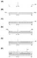
≪제조 방법 2≫
다음에, 도 4 및 도 5를 사용하여 도 5의 (E)에 도시된 트랜지스터(150) 및 접속부(160)를 형성하는 방법을 설명한다.Next, a method of forming the
도 4의 (A)∼(E)에 도시된 기판(100), 도전막(102a) 및 도전막(102b), 절연막(104), 반도체막(106a) 및 반도체막(106b), 및 절연막(108)에 대해서는 제조 방법 1과 같은 재료, 구성, 및 방법으로 형성할 수 있다.The
<마스크 형성과 절연막의 에칭><Mask formation and insulating film etching>
절연막(108) 위에 포토리소그래피 공정으로 레지스트 마스크(210)를 형성한다(도 4의 (F) 참조). 도 4의 (F)에 도시된 바와 같이, 레지스트 마스크(210)의 두께는 영역에 따라 달라지고, 영역(210a)과, 영역(210a)의 두께보다 얇은 두께를 갖는 영역(210b)을 갖는다. 영역(210b)은 반도체막(106a) 및 반도체막(106b)과 중첩되는 부분을 갖는다.A resist
레지스트 마스크(210)는 다계조 마스크(하프톤 포토마스크 또는 그레이톤 포토마스크)를 사용한 포토리소그래피 공정으로 형성한다.The resist
다음에, 절연막(104) 및 절연막(108) 중 도전막(102a)과 중첩되며 레지스트 마스크(210)와 중첩되지 않는 부분을 에칭하여 제거함으로써 개구(111b)를 형성한다(도 5의 (A) 참조).Next, a portion of the insulating
다음에, 레지스트 마스크(210)에 대하여 애싱을 수행한다. 이로써, 레지스트 마스크(210)의 면적(3차원적으로 보면 체적)이 축소되어 두께가 얇아진다. 그러므로 두께가 얇은 영역(210b)의 레지스트 마스크(210)가 제거되어 레지스트 마스크(212)가 형성된다(도 5의 (B) 참조). 즉, 레지스트 마스크(210)를 후퇴시킴으로써 영역(210b)의 레지스트 마스크(210)를 제거하여 레지스트 마스크(212)를 형성한다.Next, ashing is performed on the resist
애싱은, 예를 들어 산소 플라즈마에 의한 애싱을 수행할 수 있다.As for ashing, ashing with oxygen plasma can be performed, for example.
다음에, 절연막(108) 중 레지스트 마스크(212)와 중첩되지 않는 부분을 에칭하여 제거함으로써 개구(211a), 개구(211b), 개구(211c), 개구(211d)를 형성한다(도 5의 (C) 참조).Next, portions of the insulating
도 5의 (C)에 도시된 바와 같이, 개구(211a), 개구(211c), 개구(211d)는 절연막(108) 중 반도체막(106a) 또는 반도체막(106b)과 중첩되며 레지스트 마스크(212)와 중첩되지 않는 부분을 제거함으로써 형성된다.As shown in FIG. 5C, the
또한, 개구(211b)는 절연막(108) 중 반도체막(106a), 반도체막(106b), 및 레지스트 마스크(212)와 중첩되지 않는 부분이 제거됨으로써 형성된다. 도 5의 (C)에 도시된 바와 같이, 개구(211b)는 개구(111b)의 주위의 절연막(108)이 제거되어 개구가 넓게 되어 형성된다. 이로써, 나중의 공정으로 개구(211b) 내 및 위에 형성하는 도전막의 단절이 억제된다.In addition, the
다음에, 레지스트 마스크(212)를 제거한다(도 5의 (D) 참조).Next, the resist
<도전막 형성><Formation of conductive film>
다음에, 절연막(108), 반도체막(106a), 반도체막(106b), 및 도전막(102a)의 위에 도전막을 형성하고, 이 도전막 위에 포토리소그래피 공정으로 레지스트 마스크를 형성한다. 다음에, 이 레지스트 마스크를 사용하여 도전막의 일부를 에칭하여 도전막(114a), 도전막(114b), 도전막(114c)을 형성한다(도 5의 (E) 참조).Next, a conductive film is formed on the insulating
도전막(114a), 도전막(114b), 도전막(114c)은 제조 방법 1과 같은 재료, 구성, 및 방법으로 형성할 수 있다.The
상술한 공정을 거쳐 트랜지스터(150) 및 접속부(160)를 형성할 수 있다.The
상술한 바와 같이 제조 방법 2에서는 다계조 마스크를 사용함으로써 개구(211a), 개구(211b), 개구(211c), 개구(211d)를 하나의 마스크로 형성할 수 있다. 또한, 개구(211b)에서는, 절연막(104)의 개구보다 절연막(108)의 개구가 넓게 되도록 형성될 수 있어, 도전막(114a)의 단절을 억제할 수 있다.As described above, in
이러한 공정으로 함으로써 마스크 및 포토리소그래피 공정 수를 삭감할 수 있다. 그러므로, 반도체 장치의 제조 시간을 단축하고 제조 비용을 억제할 수 있다. 또한, 반도체 장치의 수율 및 신뢰성을 향상시킬 수 있다.By setting it as such a process, the number of mask and photolithography processes can be reduced. Therefore, it is possible to shorten the manufacturing time of the semiconductor device and suppress the manufacturing cost. Further, it is possible to improve the yield and reliability of the semiconductor device.
≪제조 방법 3≫
다음에, 도 6 및 도 7을 사용하여 도 7의 (E)에 도시된 트랜지스터(150) 및 접속부(160)를 형성하는 방법을 설명한다.Next, a method of forming the
도 6의 (A)∼(C)에 도시된 기판(100), 도전막(102a) 및 도전막(102b), 및 절연막(104)에 대해서는 제조 방법 1과 같은 재료, 구성, 및 방법으로 형성할 수 있다.The
<반도체막 형성><Semiconductor film formation>
절연막(104) 위에 반도체막(106)을 형성한다. 반도체막(106)에 대해서는 제조 방법 1과 같은 재료, 구성, 및 방법으로 형성할 수 있다.A
<마스크 형성과 절연막 및 반도체막의 에칭><Mask formation and etching of insulating and semiconductor films>
다음에, 반도체막(106) 위에 포토리소그래피 공정으로 레지스트 마스크(307)를 형성한다(도 6의 (D) 참조). 도 6의 (D)에 도시된 바와 같이, 레지스트 마스크(307)의 두께는 영역에 따라 달라지고, 영역(307a)과, 영역(307a)의 두께보다 얇은 두께를 갖는 영역(307b)을 갖는다. 영역(307b)은 반도체막(106)과 중첩되는 부분을 갖는다.Next, a resist
레지스트 마스크(307)는 다계조 마스크(하프톤 포토마스크 또는 그레이톤 포토마스크)를 사용한 포토리소그래피 공정으로 형성한다.The resist
다음에, 절연막(104) 및 반도체막(106) 중 도전막(102a)과 중첩되며 레지스트 마스크(307)와 중첩되지 않는 부분을 에칭하여 제거함으로써 개구(308b)를 형성한다(도 6의 (E) 참조).Next, an
다음에, 레지스트 마스크(307)에 대하여 애싱을 수행한다. 이로써, 레지스트 마스크(307)의 면적(3차원적으로 보면 체적)이 축소되어 두께가 얇아진다. 그러므로 두께가 얇은 영역(307b)의 레지스트 마스크(307)가 제거되어 레지스트 마스크(309)가 형성된다(도 7의 (A) 참조). 즉, 레지스트 마스크(307)를 후퇴시킴으로써 영역(307b)의 레지스트 마스크(307)를 제거하여 레지스트 마스크(309)를 형성한다.Next, ashing is performed on the resist
애싱은, 예를 들어 산소 플라즈마에 의한 애싱을 수행할 수 있다.As for ashing, ashing with oxygen plasma can be performed, for example.
다음에, 반도체막(106) 중 레지스트 마스크(309)와 중첩되지 않는 부분을 에칭하여 제거함으로써 반도체막(106a) 및 반도체막(106b)을 형성한다(도 7의 (B) 참조). 반도체막(106b)은 트랜지스터(150)에서의 채널 영역을 포함하는 반도체막으로서 기능할 수 있다.Next, the
다음에 레지스트 마스크(309)를 제거한다(도 7의 (C) 참조).Next, the resist
<절연막 형성><Insulation film formation>
다음에, 절연막(104), 반도체막(106a), 및 반도체막(106b) 위에 절연막을 형성하고, 이 절연막 위에 포토리소그래피 공정으로 레지스트 마스크를 형성한다. 그 다음에 이 레지스트 마스크를 사용하여 절연막의 일부를 에칭하여 개구(311a), 개구(311b), 개구(311c), 개구(311d)를 갖는 절연막(108)을 형성한다(도 7의 (D) 참조).Next, an insulating film is formed over the insulating
도 7의 (D)에 도시된 바와 같이, 개구(311a), 개구(311c), 개구(311d)는 반도체막(106a) 또는 반도체막(106b)과 중첩되는 부분에 형성된다.As shown in Fig. 7D, the
또한, 개구(311b)는 반도체막(106a) 및 반도체막(106b)과 중첩되지 않는 부분이 제거됨으로써 형성된다. 또한, 도 7의 (D)에 도시된 바와 같이, 개구(311b)는 개구(308b)와 중첩되는 부분에 형성된다. 또한, 개구(311b)에서는 절연막(104)의 개구보다 절연막(108)의 개구가 넓게 되도록 형성될 수 있다. 이로써, 나중의 공정으로 개구(311b) 내 및 위에 형성하는 도전막의 단절이 억제된다.Further, the
절연막(108)은 트랜지스터(150)에서 반도체막(106b)의 채널 영역을 보호하는 막으로서 기능하고, 제조 방법 1과 같은 재료, 구성, 및 방법으로 형성할 수 있다.The insulating
<도전막 형성><Formation of conductive film>
다음에, 절연막(108), 반도체막(106a), 반도체막(106b), 및 도전막(102a) 위에 도전막을 형성하고, 이 도전막 위에 포토리소그래피 공정으로 레지스트 마스크를 형성한다. 다음에, 이 레지스트 마스크를 사용하여 도전막의 일부를 에칭하여 도전막(114a), 도전막(114b), 도전막(114c)을 형성한다(도 7의 (E) 참조).Next, a conductive film is formed over the insulating
도전막(114a), 도전막(114b), 도전막(114c)은 제조 방법 1과 같은 재료, 구성, 및 방법으로 형성할 수 있다.The
상술한 공정을 거쳐 트랜지스터(150) 및 접속부(160)를 형성할 수 있다.The
상술한 바와 같이 제조 방법 3에서는 하프톤 포토마스크를 사용함으로써 절연막(104)의 개구와 반도체막(106a) 및 반도체막(106b)을 하나의 마스크로 형성할 수 있다. 또한, 개구(311b)에서는, 절연막(104)의 개구보다 절연막(108)의 개구가 넓게 되도록 형성될 수 있어, 도전막(114a)의 단절을 억제할 수 있다.As described above, in
이러한 공정으로 함으로써 마스크 및 포토리소그래피 공정 수를 삭감할 수 있다. 그러므로, 반도체 장치의 제조 시간을 단축하고 제조 비용을 억제할 수 있다. 또한, 반도체 장치의 수율 및 신뢰성을 향상시킬 수 있다.By setting it as such a process, the number of mask and photolithography processes can be reduced. Therefore, it is possible to shorten the manufacturing time of the semiconductor device and suppress the manufacturing cost. Further, it is possible to improve the yield and reliability of the semiconductor device.
<개구의 베리에이션><Variation of openings>
또한, 레지스트 마스크(307)의 형상을 변경함으로써, 도 7의 (E)에 도시된 접속부(160)와 다른 형상을 가진 도 8의 (D)에 도시된 접속부(160)를 형성할 수 있다.In addition, by changing the shape of the resist
우선, 레지스트 마스크(307)를 도 8의 (A)에 도시된 바와 같은 형상(예를 들어 도 6의 (E)에 도시된 것보다 넓은 개구를 갖는 형상)으로 하여 개구(308b)를 형성한다(도 8의 (A) 참조).First, the resist
그 다음에, 도 7의 (A)∼(C)와 같은 공정으로 반도체막(106a) 및 반도체막(106b)을 형성한다(도 8의 (B) 참조).Then, the
다음에, 절연막(104), 반도체막(106a) 및 반도체막(106b) 위에 절연막을 형성하고, 이 절연막 위에 포토리소그래피 공정으로 레지스트 마스크를 형성한다. 다음에, 이 레지스트 마스크를 사용하여 절연막의 일부를 에칭하여 개구(311a), 개구(312b), 개구(311c), 개구(311d)를 갖는 절연막(108)을 형성한다. 이 때, 절연막(108)에서의 개구(312b)가 절연막(104)에서의 개구(308b)보다 작게 되도록 형성한다.Next, an insulating film is formed over the insulating
상술한 공정을 거쳐 도 8의 (D)에 도시된 접속부(160)를 형성할 수 있다.The
이러한 공정으로 하여도 절연막(104)의 개구와 반도체막(106a) 및 반도체막(106b)을 하나의 마스크로 형성하고, 또한 도전막(114a)의 단절을 억제할 수 있다. 그러므로, 마스크 및 포토리소그래피 공정 수를 삭감하고 반도체 장치의 제조 시간을 단축하며, 제조 비용을 억제할 수 있다. 또한, 반도체 장치의 수율 및 신뢰성을 향상시킬 수 있다.Even with such a process, the opening of the insulating
≪제조 방법 4≫≪Production method 4≫
다음에, 도 9 및 도 10을 사용하여 도 10의 (E)에 도시된 트랜지스터(150) 및 접속부(160)를 형성하는 방법을 설명한다.Next, a method of forming the
도 9의 (A)∼(F) 및 도 10의 (A)에 도시된 기판(100), 도전막(102a) 및 도전막(102b), 절연막(104), 반도체막(106a) 및 반도체막(106b), 절연막(108), 개구(111a), 개구(111b), 개구(111c), 및 개구(111d)에 대해서는 제조 방법 1과 같은 재료, 구성, 및 방법으로 형성할 수 있다.The
<마스크의 애싱><Ashing of the mask>
도 10의 (A)에 도시된 바와 같이 레지스트 마스크(110)를 사용하여 개구(111a), 개구(111b), 개구(111c), 및 개구(111d)를 형성한 후에 레지스트 마스크(110)에 대하여 애싱을 수행한다. 애싱은, 예를 들어 산소 플라즈마에 의한 애싱을 수행할 수 있다.10A, after forming the
이로써, 레지스트 마스크(110)의 면적(3차원적으로 보면 체적)이 축소되어 두께가 얇아져서 레지스트 마스크(412)가 형성된다(도 10의 (B) 참조). 이로써, 절연막(108)의 일부에 레지스트 마스크(412)와 중첩되지 않는 부분이 생긴다. 즉, 레지스트 마스크(110)를 후퇴시킴으로써 절연막(108)의 일부가 노출된다.As a result, the area (volume in three dimensions) of the resist
다음에, 절연막(108) 중 레지스트 마스크(412)와 중첩되지 않는 부분을 에칭하여 제거함으로써 개구(411a), 개구(411b), 개구(411c), 및 개구(411d)를 형성한다(도 10의 (C) 참조).Next, the portions of the insulating
도 10의 (C)에 도시된 바와 같이, 개구(411a), 개구(411c), 및 개구(411d)는 반도체막(106a) 또는 반도체막(106b)과 중첩되는 부분에 형성된다.As shown in Fig. 10C, the
또한, 개구(411b)는 도전막(102a)과 중첩되며 반도체막(106a) 및 반도체막(106b)과 중첩되지 않는 부분이 제거됨으로써 형성된다. 또한, 도 10의 (C)에 도시된 바와 같이, 개구(411b)는 개구(111b)의 주위의 절연막(108)이 제거되어 개구가 넓게 되어 형성된다. 이로써, 나중의 공정으로 개구(411b) 내 및 위에 형성하는 도전막의 단절을 억제할 수 있다.Further, the
또한, 레지스트 마스크(110)를 애싱함으로써 레지스트 마스크(412)가 형성되므로, 레지스트 마스크(110)와 레지스트 마스크(412)의 크기의 차이들, 즉, 레지스트 마스크(412)로 덮이지 않는 절연막(108)의 폭들은, 실질적으로 균일하게 된다.In addition, since the resist
그러므로, 개구(411b)에서 절연막(104)과 절연막(108)이 형성하는 단차의 폭, 즉, 도 10의 (C)에 도시된 L은 개구(411b)의 주위에 있어서 실질적으로 균일하게 된다.Therefore, the width of the step formed by the insulating
다음에 레지스트 마스크(412)를 제거한다(도 10의 (D) 참조).Next, the resist
<도전막 형성><Formation of conductive film>
다음에, 절연막(108), 반도체막(106a), 반도체막(106b), 및 도전막(102a) 위에 도전막을 형성하고, 이 도전막 위에 포토리소그래피 공정으로 레지스트 마스크를 형성한다. 다음에, 이 레지스트 마스크를 사용하여 도전막의 일부를 에칭하여 도전막(114a), 도전막(114b), 도전막(114c)을 형성한다(도 10의 (E) 참조).Next, a conductive film is formed over the insulating
도전막(114a), 도전막(114b), 도전막(114c)은 제조 방법 1과 같은 재료, 구성, 및 방법으로 형성할 수 있다.The
상술한 공정을 거쳐 트랜지스터(150) 및 접속부(160)를 형성할 수 있다.The
상술한 바와 같이 제조 방법 4로는, 절연막(108) 중 반도체막과 중첩되는 부분에 개구를 형성함과 동시에 반도체막과 중첩되지 않는 부분에서는 절연막(108)뿐만 아니라 절연막(104)에도 개구를 형성한다. 이와 같은 공정으로 함으로써 절연막(108)과 절연막(104)의 개구를 따로따로 형성하는 경우에 비하여, 마스크 및 포토리소그래피 공정 수를 삭감할 수 있다. 또한, 레지스트 마스크(110)를 애싱함으로써 개구(411b)에서 절연막(104)의 개구보다 절연막(108)의 개구가 넓게 되도록 할 수 있고, 도전막(114a)의 단절을 억제할 수 있다.As described above, in the manufacturing method 4, an opening is formed in a portion of the insulating
이러한 공정으로 함으로써 마스크 및 포토리소그래피 공정 수를 삭감할 수 있다. 그러므로, 반도체 장치의 제조 시간을 단축하고 제조 비용을 억제할 수 있다. 또한, 반도체 장치의 수율 및 신뢰성을 향상시킬 수 있다.By setting it as such a process, the number of mask and photolithography processes can be reduced. Therefore, it is possible to shorten the manufacturing time of the semiconductor device and suppress the manufacturing cost. Further, it is possible to improve the yield and reliability of the semiconductor device.
(실시형태 2)(Embodiment 2)
본 발명의 일 형태인 반도체 장치의 제조 방법에 대하여 도 1, 도 11, 및 도 12를 사용하여 설명한다. 도 1은 상술한 바와 같이 반도체 장치의 상면도이다. 도 1의 (A) 중 일점 쇄선 X1-X2부분의 단면 구조를 도 11 및 도 12의 단면 X1-X2에서 도시하였다. 단면 X1-X2는 트랜지스터와, 트랜지스터 위에 제공된 도전막이 전기적으로 접속되는 영역의 일부의 단면 구조이다. 도 1의 (B) 중 일점 쇄선 Y1-Y2부분의 단면 구조를 도 11 및 도 12의 단면 Y1-Y2에서 도시하였다. 단면 Y1-Y2는 반도체막 아래에 제공된 도전막과 반도체막 위에 제공된 도전막이 전기적으로 접속되는 영역의 일부의 단면 구조이다. 도 1의 (C) 중 일점 쇄선 Z1-Z2부분의 단면 구조를 도 11 및 도 12의 단면 Z1-Z2에서 도시하였다. 단면 Z1-Z2는 트랜지스터의 소스 전극 및 드레인 전극으로서 기능할 수 있는 도전막과 동시에 형성된 도전막과, 트랜지스터 위에 형성된 2개의 도전막이 전기적으로 접속된 영역의 일부의 단면 구조이다.A method of manufacturing a semiconductor device according to an embodiment of the present invention will be described with reference to FIGS. 1, 11 and 12. 1 is a top view of a semiconductor device as described above. A cross-sectional structure of a portion of the dashed-dotted line X1-X2 in FIG. 1A is shown in cross-sections X1-X2 of FIGS. 11 and 12. Cross-sections X1-X2 are cross-sectional structures of a portion of a region to which the transistor and the conductive film provided on the transistor are electrically connected. The cross-sectional structure of a portion of the dashed-dotted line Y1-Y2 in FIG. 1B is shown in cross-sections Y1-Y2 in FIGS. 11 and 12. Cross-sections Y1-Y2 are cross-sectional structures of a portion of a region in which the conductive film provided under the semiconductor film and the conductive film provided over the semiconductor film are electrically connected. The cross-sectional structure of portions Z1-Z2 of the dashed-dotted line in FIG. 1C is shown in cross-sections Z1-Z2 of FIGS. 11 and 12. Cross-sections Z1-Z2 are cross-sectional structures of a part of a region in which a conductive film formed simultaneously with a conductive film that can function as a source electrode and a drain electrode of a transistor, and two conductive films formed on the transistor are electrically connected.
본 실시형태에서 제시하는 반도체 장치의 제조 방법은 트랜지스터 위에 복수의 도전막을 형성하는 경우에 적용할 수 있다. 예를 들어, 동일 기판 위에 공통 전극과 화소 전극을 형성하는 IPS(In Plane Switching)(또는 FFS(Fringe Field Switching)) 모드의 액정 표시 장치 등에 적합하다.The method of manufacturing a semiconductor device presented in the present embodiment can be applied when forming a plurality of conductive films on a transistor. For example, it is suitable for a liquid crystal display device of an IPS (In Plane Switching) (or FFS (Fringe Field Switching)) mode in which a common electrode and a pixel electrode are formed on the same substrate.
≪제조 방법 5≫≪Production method 5≫
도 11 및 도 12를 사용하여 도 12의 (E)에 도시된 접속부(550) 및 접속부(560)를 형성하는 방법을 설명한다.A method of forming the
<하부 구성><Substructure>
우선, 도전막이 제공된 기판을 준비한다. 상기 기판은 실시형태 1에서 제시한 트랜지스터(150) 및 접속부(160)가 형성된 기판이라도 좋고 다른 방법 및 구성으로 도전막이 형성된 기판이라도 좋다. 예를 들어 실시형태 1에서 제시한 보텀 게이트 구조의 트랜지스터(150)에 한정되지 않으며 톱 게이트 구조의 트랜지스터가 형성된 기판을 사용하여도 좋다.First, a substrate provided with a conductive film is prepared. The substrate may be a substrate on which the
본 실시형태에서는 실시형태 1에서 제시한 제조 방법 2와 마찬가지로, 단면 X1-X2에 트랜지스터(150), 단면 Y1-Y2에 접속부(160)가 형성되고, 또한 제조 방법 2와 같은 공정을 거쳐 단면 Z1-Z2에 절연막(104), 절연막(108) 및 도전막(114d)이 형성된 기판을 준비한다(도 11의 (A) 참조). 도전막(114d)은 도전막(114a), 도전막(114b), 도전막(114c)과 같은 재료, 구성, 및 방법으로 형성할 수 있다. 상기 기판의 도전막(114a) 및 도전막(114d) 위에는, 이하에서 제시하는 공정을 거쳐 접속부(550) 및 접속부(560)를 형성한다.In this embodiment, in the same manner as in the
<절연막 형성><Insulation film formation>
도전막(114a), 도전막(114b), 도전막(114c), 및 도전막(114d) 위에 절연막(500)을 형성한다(도 11의 (B) 참조). 절연막(500)은 실시형태 1에서 제시한 절연막(104)과 같은 재료, 구성, 및 방법으로 형성할 수 있다.An insulating
<절연막 형성><Insulation film formation>
다음에 절연막(500) 위에 절연막(502)을 형성한다(도 11의 (C) 참조). 절연막(502)은 반도체 장치에서의 평탄화막으로서 기능할 수 있다.Next, an insulating
절연막(502)으로서는 예를 들어 아크릴, 아크릴아마이드, 에스테르, 기타 공지의 재료가 사용될 수 있고, 적층 또는 단층으로 제공된다.As the insulating
<도전막 형성><Formation of conductive film>
다음에, 절연막(502) 위에 도전막(504)을 형성한다(도 11의 (D) 참조). 도전막(504)으로서는 투광성을 갖는 재료를 사용하는 것이 바람직하다.Next, a
도전막(504)에는, 산화 텅스텐을 포함한 인듐 산화물, 산화 텅스텐을 포함한 인듐 아연 산화물, 산화 티타늄을 포함한 인듐 산화물, 산화 티타늄을 포함한 인듐 주석 산화물, 인듐 주석 산화물(이하, ITO라고 나타냄), 인듐 아연 산화물, 산화 실리콘을 첨가한 인듐 주석 산화물 등의 투광성을 갖는 도전성 재료를 사용할 수 있다.The
또한, 도전막(504)은, 도전성 고분자(도전성 폴리머라고도 함)를 포함한 도전성 조성물을 사용하여 형성할 수 있다. 도전성 조성물을 사용하여 형성한 투광성 도전막의 시트 저항은 10000Ω/□ 이하, 파장이 550nm인 경우의 투광률은 70% 이상인 것이 바람직하다. 또한, 도전성 조성물에 포함되는 도전성 고분자의 저항률이 0.1O·cm 이하인 것이 바람직하다.Further, the
도전성 고분자로서, 소위 π-전자 공액계 도전성 고분자를 사용할 수 있다. 예를 들어, 폴리아닐린 또는 그 유도체, 폴리피롤 또는 그 유도체, 폴리티오펜 또는 그 유도체, 아닐린, 피롤, 및 티오펜의 2개 이상으로 이루어진 공중합체 또는 그 유도체 등을 들 수 있다.As the conductive polymer, a so-called π-electron conjugated conductive polymer can be used. For example, polyaniline or a derivative thereof, polypyrrole or a derivative thereof, polythiophene or a derivative thereof, a copolymer composed of two or more of aniline, pyrrole, and thiophene, or a derivative thereof, may be mentioned.
도전막(504)은, 상술한 재료를 적층 또는 단층으로 하여 제공할 수 있다.The
<마스크 형성과 도전막 및 절연막의 에칭><Mask formation and etching of conductive and insulating films>
다음에, 도전막(504) 위에 포토리소그래피 공정으로 레지스트 마스크(506)를 형성한다(도 11의 (E) 참조). 도 11의 (E)에 도시된 바와 같이, 레지스트 마스크(506)의 두께는 영역에 따라 달라지고, 영역(506a)과, 영역(506a)의 두께보다 얇은 두께를 갖는 영역(506b)을 갖는다. 영역(506b)은 도전막(504)과 중첩되는 부분을 갖는다.Next, a resist
레지스트 마스크(506)는 다계조 마스크(하프톤 포토마스크 또는 그레이톤 포토마스크)를 사용한 포토리소그래피 공정으로 형성한다.The resist
다음에, 절연막(500), 절연막(502), 및 도전막(504) 중 레지스트 마스크(506)와 중첩되지 않는 부분을 에칭하여 제거함으로써 개구(507a) 및 개구(507c)를 형성한다(도 12의 (A) 참조).Next, the portions of the insulating
다음에, 레지스트 마스크(506)에 대하여 애싱을 수행한다. 이로써, 레지스트 마스크(506)의 면적(3차원적으로 보면 체적)이 축소되어 두께가 얇아진다. 그러므로 두께가 얇은 영역(506b)의 레지스트 마스크(506)가 제거되어 레지스트 마스크(508)가 형성된다(도 12의 (B) 참조). 즉, 레지스트 마스크(506)를 후퇴시킴으로써 영역(506b)의 레지스트 마스크(506)를 제거하여 레지스트 마스크(508)를 형성한다.Next, ashing is performed on the resist
애싱은, 예를 들어 산소 플라즈마에 의한 애싱을 수행할 수 있다.As for ashing, ashing with oxygen plasma can be performed, for example.
다음에, 도전막(504) 중 레지스트 마스크(508)와 중첩되지 않는 부분을 에칭하여 제거하고, 이 후에 레지스트 마스크(508)를 제거하여 도전막(504a)을 형성한다(도 12의 (C) 참조). 도전막(504a)은 액정 표시 장치에서의 공통 전극으로서 기능할 수 있다.Next, a portion of the
<절연막 형성><Insulation film formation>
다음에, 도전막(504a), 절연막(502), 절연막(500), 도전막(114d), 및 도전막(114c) 위에 절연막을 형성하고, 이 절연막 위에 포토리소그래피 공정으로 레지스트 마스크를 형성한다. 그 다음에 이 레지스트 마스크를 사용하여 절연막의 일부를 에칭하여 절연막(510)을 형성한다(도 12의 (D) 참조). 도 12의 (D)에 도시된 바와 같이 절연막(510)에서는 개구(507a)와 중첩되는 부분에 개구(511a)가 형성되고, 도전막(504a)과 중첩되는 부분에 개구(511b)가 형성된다. 또한, 개구(507c)와 중첩되는 부분에 개구(511c)가 형성된다.Next, an insulating film is formed over the
절연막(510)은 실시형태 1에서 제시한 절연막(104)과 같은 재료, 구성, 및 방법으로 형성할 수 있다.The insulating
<도전막 형성><Formation of conductive film>
다음에, 절연막(510), 도전막(504a), 절연막(502), 절연막(500), 도전막(114d), 및 도전막(114c) 위에 도전막을 형성하고, 이 도전막 위에 포토리소그래피 공정으로 레지스트 마스크를 형성한다. 그 다음에 이 레지스트 마스크를 사용하여 도전막의 일부를 에칭하여 도전막(512a) 및 도전막(512b)을 형성한다(도 12의 (E) 참조).Next, a conductive film is formed on the insulating
도전막(512a)은 도전막(114d) 및 도전막(504a)과 전기적으로 접속된다. 또한, 도전막(512b)은 도전막(114c)과 전기적으로 접속된다. 도전막(512b)은 액정 표시 장치에서의 화소 전극으로서 기능할 수 있다. 또한, 도시하지 않았지만 도전막(504a)과 도전막(512b)이 중첩된 부분은 용량 소자로서 기능할 수 있다. 다만, 이에 한정되지 않으며 용량 소자는 도전막(504a)과 도전막(512b)이 중첩된 부분 외에서 형성되어도 좋다. 예를 들어 도전막(504a)과 따로 형성한 도전막이 중첩된 부분이 용량 소자로서 기능하여도 좋다.The
도전막(512a) 및 도전막(512b)은 도전막(504a)과 같은 재료, 구성, 및 방법으로 형성할 수 있다.The
상술한 공정을 거쳐 접속부(550) 및 접속부(560)를 형성할 수 있다.The
상술한 바와 같이 제조 방법 5에서는 하프톤 포토마스크를 사용함으로써 개구(507a) 및 개구(507c)와, 도전막(504a)을 하나의 마스크로 형성할 수 있다.As described above, in Manufacturing Method 5, by using a halftone photomask, the
이러한 공정으로 함으로써 마스크 및 포토리소그래피 공정 수를 삭감할 수 있다. 그러므로, 반도체 장치의 제조 시간을 단축하고 제조 비용을 억제할 수 있다.By setting it as such a process, the number of mask and photolithography processes can be reduced. Therefore, it is possible to shorten the manufacturing time of the semiconductor device and suppress the manufacturing cost.
(실시형태 3)(Embodiment 3)
실시형태 2에서 설명한 본 발명의 일 형태인 반도체 장치의 제조 방법의 다른 형태에 대하여 도 1 및 도 15를 사용하여 설명한다. 도 1은 상술한 바와 같이 반도체 장치의 상면도이다. 도 1의 (A) 중 일점 쇄선 X1-X2부분의 단면 구조를 도 15의 단면 X1-X2에서 도시하였다. 단면 X1-X2는 트랜지스터와, 트랜지스터 위에 제공된 도전막이 전기적으로 접속되는 영역의 일부의 단면 구조이다. 도 1의 (B) 중 일점 쇄선 Y1-Y2부분의 단면 구조를 도 15의 단면 Y1-Y2에서 도시하였다. 단면 Y1-Y2는 반도체막 아래에 제공된 도전막과 반도체막 위에 제공된 도전막이 전기적으로 접속되는 영역의 일부의 단면 구조이다. 도 1의 (C) 중 일점 쇄선 Z1-Z2부분의 단면 구조를 도 15의 단면 Z1-Z2에서 도시하였다. 단면 Z1-Z2는 트랜지스터의 소스 전극 및 드레인 전극으로서 기능할 수 있는 도전막과 동시에 형성된 도전막과, 트랜지스터 위에 형성된 2개의 도전막이 전기적으로 접속된 영역의 일부의 단면 구조이다.Another form of a method for manufacturing a semiconductor device according to an embodiment of the present invention described in
본 실시형태에서 제시하는 반도체 장치의 제조 방법은 트랜지스터 위에 복수의 도전막을 형성하는 경우에 적용할 수 있다. 예를 들어, 동일 기판 위에 공통 전극과 화소 전극을 형성하는 IPS(In Plane Switching)(또는 FFS(Fringe Field Switching)) 모드의 액정 표시 장치 등에 적합하다.The method of manufacturing a semiconductor device presented in the present embodiment can be applied when forming a plurality of conductive films on a transistor. For example, it is suitable for a liquid crystal display device of an IPS (In Plane Switching) (or FFS (Fringe Field Switching)) mode in which a common electrode and a pixel electrode are formed on the same substrate.
≪제조 방법 6≫≪Manufacturing method 6≫
도 15를 사용하여 도 15의 (C)에 도시된 접속부(650) 및 접속부(660)를 형성하는 방법을 설명한다. 본 실시형태에서 제시하는 본 발명의 일 형태인 반도체 장치의 제조 방법은 도전막(504a)을 형성할 때까지의 공정은 실시형태 2에서 제시한 제조 방법 5와 마찬가지이므로, 상기 기재를 참조하기 바란다. 도 15의 (A)는 도전막(504a)까지를 형성한 상태의 단면 구조이다. 도전막(504a), 개구(507a), 및 개구(507c)는 하나의 다계조 마스크(하프톤 포토마스크 또는 그레이톤 포토마스크)를 사용하여 형성되어 있으므로, 마스크 및 포토리소그래피 공정 수를 삭감할 수 있다. 그러므로, 반도체 장치의 제조 시간을 단축하고 제조 비용을 억제할 수 있다.A method of forming the
<절연막 형성><Insulation film formation>
다음에, 도전막(504a), 절연막(502), 절연막(500), 도전막(114d), 및 도전막(114c) 위에 절연막을 형성하고 이 절연막 위에 포토리소그래피 공정으로 레지스트 마스크를 형성한다. 다음에, 상기 레지스트 마스크를 사용하여 절연막의 일부를 에칭하여 절연막(610)을 형성한다(도 15의 (B) 참조). 도 15의 (B)에 도시된 바와 같이 절연막(610)에서는 개구(507a)의 내부에 개구(611a)가 형성되어 있고, 도전막(504a)과 중첩되는 부분에 개구(511b)가 형성된다. 또한, 개구(507c)의 내부에 개구(611c)가 형성되어 있다.Next, an insulating film is formed over the
실시형태 2에서 제시한 제조 방법 5와 달리, 절연막(610)이 개구(507a) 및 개구(507c)의 내부에도 형성되어 있다. 그러므로, 개구(507a) 및 개구(507c)에 있어서의 절연막(502)의 측면은 절연막(610)으로 덮인다. 이와 같은 구조로 함으로써 절연막(502) 내부의 불순물이나, 개구(507a) 및 개구(507c)에서의 절연막(502)의 측면에 상술한 다계조 마스크의 애싱 공정 등으로 부착된 불순물 등이 절연막(502) 외부의 방향으로 확산되는 것을 억제할 수 있다. 예를 들어, 후술하는 실시형태 4에서 제시하는 액정 표시 장치에서 상기 불순물이 액정에 혼입되면 액정의 열화가 일어난다. 절연막(502)이 상기 불순물의 확산을 억제할 수 있으므로 액정 표시 장치의 열화를 억제할 수 있다.Unlike the manufacturing method 5 suggested in
<도전막 형성><Formation of conductive film>
다음에, 절연막(610), 도전막(504a), 절연막(502), 절연막(500), 도전막(114d), 및 도전막(114c) 위에 도전막을 형성하고 이 도전막 위에 포토리소그래피 공정으로 레지스트 마스크를 형성한다. 다음에, 레지스트 마스크를 사용하여 도전막의 일부를 에칭함으로써 도전막(612a) 및 도전막(612b)을 형성한다(도 15의 (C) 참조).Next, a conductive film is formed on the insulating film 610, the
도전막(612a)은 도전막(114d) 및 도전막(504a)과 전기적으로 접속된다. 또한, 도전막(612b)은 도전막(114c)과 전기적으로 접속된다. 도전막(612b)은 액정 표시 장치에서의 화소 전극으로서 기능할 수 있다. 또한, 도시하지 않았지만 도전막(504a)과 도전막(612b)이 서로 중첩된 부분은 용량 소자로서 기능할 수 있다. 다만, 이에 한정되지 않으며 용량 소자는 도전막(504a)과 도전막(612b)이 중첩된 부분 이외에서 형성되어도 좋다. 예를 들어 도전막(504a)과 따로 형성한 도전막이 중첩된 부분이 용량 소자로서 기능하여도 좋다.The
도전막(612a) 및 도전막(612b)은 도전막(504a)과 같은 재료, 구성, 및 방법으로 형성할 수 있다.The
상술한 공정을 거쳐 접속부(650) 및 접속부(660)를 형성할 수 있다.The
또한, 도 15에 도시된 단면도를 보면 알 수 있듯이, 접속부(650) 및 접속부(660)에서 절연막(500), 절연막(502), 및 절연막(610)은 측면에 테이퍼 형상을 가져도 좋다. 절연막(500), 절연막(502), 및 절연막(610)은 측면이 테이퍼 형상을 갖는 경우, 접속부(650) 및 접속부(660)에서 도전막(612a) 및 도전막(612b)도 테이퍼 형상을 가지게 된다. 접속부(650) 및 접속부(660)에서 절연막(500), 절연막(502), 및 절연막(610)의 측면이 수직 형상인 경우, 도전막(612a) 및 도전막(612b)이 충분히 형성되지 않아 단절이 발생될 우려가 있다. 한편, 절연막(500), 절연막(502), 및 절연막(610)의 측면이 테이퍼 형상을 가지면 도전막(612a) 및 도전막(612b)의 단절을 방지할 수 있으며 반도체 장치의 신뢰성을 향상시킬 수 있다.Further, as can be seen from the cross-sectional view of FIG. 15, the insulating
이런 제조 방법 6으로는 하프톤 포토마스크를 사용함으로써 개구(507a) 및 개구(507c)와, 도전막(504a)을 하나의 마스크로 형성할 수 있다. 또한 절연막(502)의 측면으로부터 불순물이 확산되는 것을 억제할 수 있다.In the manufacturing method 6, by using a halftone photomask, the
상술한 공정으로 함으로써 마스크 및 포토리소그래피 공정 수를 삭감할 수 있다. 그러므로, 반도체 장치의 제조 시간을 단축하고 제조 비용을 억제할 수 있다. 또한, 신뢰성을 저하시키지 않고 반도체 장치를 이용할 수 있다.By setting it as the above-described process, the number of mask and photolithography processes can be reduced. Therefore, it is possible to shorten the manufacturing time of the semiconductor device and suppress the manufacturing cost. Further, a semiconductor device can be used without deteriorating the reliability.
(실시형태 4)(Embodiment 4)
본 실시형태에서는 실시형태 1∼실시형태 3에서 제시한 반도체 장치의 제조 방법을 적용할 수 있는, 표시 장치를 비롯한 반도체 장치에 대하여 설명한다.In this embodiment, a semiconductor device including a display device to which the method for manufacturing a semiconductor device described in Embodiments 1 to 3 can be applied will be described.
실시형태 1에서 제시한 제조 방법은 액티브 매트릭스형 액정 표시 장치의 스위칭 소자의 제조 방법으로서 적합하게 이용할 수 있고, TN(Twisted Nematic) 모드, VA(Vertical Alignment) 모드, IPS 모드 등 각 모드의 액정 표시 장치에 적용할 수 있다.The manufacturing method suggested in Embodiment 1 can be suitably used as a method of manufacturing a switching element of an active matrix liquid crystal display device, and liquid crystal displays in each mode such as TN (Twisted Nematic) mode, VA (Vertical Alignment) mode, IPS mode, etc. Applicable to the device.
또한, 실시형태 1에서 제시한 제조 방법은, 액티브 매트릭스형 유기 EL 소자를 사용한 발광 장치의 스위칭 소자의 제조 방법으로서도 적합하게 이용할 수 있다.In addition, the manufacturing method suggested in Embodiment 1 can be suitably used also as a manufacturing method of a switching element of a light emitting device using an active matrix type organic EL element.
또한, 실시형태 2 및 실시형태 3에서 제시한 제조 방법은 특히 IPS 모드의 액정 표시 장치의 스위칭 소자의 제조 방법으로서 적합하게 이용할 수 있고, 이 경우 화소 전극을 슬릿 형상으로 형성한다. 또한, 실시형태 2 및 실시형태 3에서 제시한 화소 전극 및 공통 전극의 적층 순서를 바꿔 공통 전극을 슬릿 형상으로 형성하여도 좋다.In addition, the manufacturing method suggested in
또한, 실시형태 1∼실시형태 3에서 제시한 제조 방법은 표시 장치 및 발광 장치에 한정되지 않고, 기억 장치, 연산 장치, CPU, 마이크로 컴퓨터 등의 반도체 장치의 제조 방법으로서도 적용할 수 있다.In addition, the manufacturing method suggested in Embodiments 1 to 3 is not limited to a display device and a light-emitting device, and can also be applied as a method for manufacturing semiconductor devices such as memory devices, computing devices, CPUs, and microcomputers.
이하에서는, 반도체 장치의 예로서, 실시형태 1에서 제시한 반도체 장치를 적용한 IPS(FFS) 모드의 액정 표시 장치(1000)에 대하여 도 13을 사용하여 설명한다.Hereinafter, as an example of a semiconductor device, a liquid
도 13의 (A)는 액정 표시 장치(1000)의 상면도이다. 도 13의 (A) 중 파선 M1-M2부분의 단면 구조를 도 13의 (B)의 단면 M1-M2에서 도시하였다. 단면 M1-M2는 실시형태 1에서 제시한 트랜지스터(150)가 형성된 영역을 포함한 단면 구조이고, 액정 표시 장치의 화소 영역으로서 기능할 수 있는 부분이다. 도 13의 (A) 중 파선 N1-N2부분의 단면 구조를 도 13의 (C)의 단면 N1-N2에서 도시하였다. 단면 N1-N2는 액정 표시 장치의 드라이버 등이 제공된 주변부 및 접속부로서 기능할 수 있는 부분이다.13A is a top view of the liquid
도 13의 (A)에 도시된 바와 같이 액정 표시 장치(1000)는 기판(1111) 및 기판(1121) 사이에 화소부(1201), 드라이버(1200) 및 드라이버(1202)를 갖는다.13A, the
또한, 도 13의 (B) 및 (C)에 도시된 바와 같이, 액정 표시 장치(1000)는 기판(1111) 위에 트랜지스터(150)를 갖는다. 또한, 액정 표시 장치(1000)는 편광판(1161), 액정층(1115), 기판(1121), 터치 패널부(1100), 접착층(1163), 편광판(1162), 및 기판(1131) 등을 갖는다. 터치 패널부(1100)는 전극(1122), 전극(1123) 등을 갖는다. 또한, 액정층의 위 및 하방에 배향막(1155) 및 배향막(1156)이 제공되고 액정층의 셀 갭을 유지하기 위하여 스페이서(1165)가 제공된다. 또한, 트랜지스터(150)와 중첩되지 않는 부분에 컬러 필터(1114)가 제공되고, 컬러 필터(1114)와 중첩되어 도전막(1113) 및 도전막(1235)이 제공된다.In addition, as shown in FIGS. 13B and 13C, the
단자부에서, 기판(1121)과 기판(1111)은 실링 부재(1421)로 접착된다. 또한, 도전막(1431) 및 도전막(1432)을 통하여 전극(1122)과 FPC(1433)는 전기적으로 접속된다. 또한, 도전막(1423)을 통하여 도전막(1422)과 FPC(1424)는 전기적으로 접속된다.In the terminal portion, the
또한, 도 13에서는 평탄화막으로서 기능할 수 있는 절연막(502)을 갖는 구조를 도시하였으나, 본 발명의 일 형태는 이에 한정되지 않고 절연막(502)을 제공하지 않는 구조의 표시 장치로 하여도 좋다.In addition, although FIG. 13 shows a structure having an insulating
(실시형태 5)(Embodiment 5)
본 실시형태에서는 본 발명의 일 형태를 적용한 액정 표시 장치를 사용한 전자 기기의 일례에 대하여 도 14를 사용하여 설명한다.In this embodiment, an example of an electronic device using a liquid crystal display device to which one embodiment of the present invention is applied will be described with reference to FIG. 14.
본 실시형태의 전자 기기는 표시부에 본 발명의 일 형태인 액정 표시 장치를 구비한다.The electronic device of this embodiment is provided with a liquid crystal display device which is one embodiment of this invention in a display part.
액정 표시 장치가 적용된 전자 기기로서 예를 들어, 텔레비전 장치(텔레비전, 또는 텔레비전 수신기라고도 함), 컴퓨터용 등의 모니터, 디지털 카메라, 디지털 비디오 카메라, 디지털 포토 프레임, 휴대 전화기(휴대 전화, 휴대 전화 장치라고도 함), 휴대형 게임기, 휴대 정보 단말, 음향 재생 장치, 파친코기 등의 대형 게임기 등을 들 수 있다. 도 14에서는 이들 전자 기기의 구체예를 도시하였다.As an electronic device to which a liquid crystal display is applied, for example, a television device (also referred to as a television or television receiver), a monitor for a computer, a digital camera, a digital video camera, a digital photo frame, a mobile phone (a mobile phone, a mobile phone device) Also referred to as), portable game machines, portable information terminals, sound reproduction devices, and large game machines such as pachinkogi. 14 shows specific examples of these electronic devices.
도 14의 (A)는 텔레비전 장치의 일례이다. 텔레비전 장치(7100)는 하우징(7101)에 표시부(7102)가 제공되어 있다. 표시부(7102)에서는 영상을 표시할 수 있다. 본 발명의 일 형태를 적용한 액정 표시 장치는 표시부(7102)에 사용할 수 있다. 또한, 여기서는 스탠드(7103)에 의하여 하우징(7101)을 지탱한 구성을 도시하였다.14A is an example of a television device. The
텔레비전 장치(7100)의 조작은, 하우징(7101)이 구비하는 조작 스위치나, 별체의 리모트 컨트롤러(7111)에 의하여 수행할 수 있다. 리모트 컨트롤러(7111)가 구비하는 조작 키를 사용하여 채널이나 음량을 조작할 수 있고, 표시부(7102)에 표시되는 영상을 조작할 수 있다. 또한, 리모트 컨트롤러(7111)에는, 이 리모트 컨트롤러(7111)로부터 출력되는 정보를 표시하는 표시부를 제공하는 구성으로 하여도 좋다.The
또한, 텔레비전 장치(7100)는, 수신기나 모뎀 등을 구비한 구성으로 한다. 수신기에 의하여 일반적인 텔레비전 방송을 수신할 수 있고, 또한 모뎀을 통하여 유선 또는 무선에 의하여 통신 네트워크에 접속됨으로써 일 방향(송신자로부터 수신자) 또는 쌍방향(송신자와 수신자간, 또는 수신자간끼리 등)의 정보 통신을 수행할 수도 있다.In addition, the
도 14의 (B)는 컴퓨터의 일례이다. 컴퓨터(7200)는 본체(7201), 하우징(7202), 표시부(7203), 키보드(7204), 외부 접속 포트(7205), 포인팅 디바이스(7206) 등을 포함한다. 또한, 컴퓨터는 본 발명의 일 형태인 액정 표시 장치를 그 표시부(7203)에 사용하여 제작된다.14B is an example of a computer. The
도 14의 (C)는 휴대형 게임기의 일례이다. 휴대형 게임기(7300)는 2개의 하우징(하우징(7301a)과 하우징(7301b))으로 구성되어 있고, 2개의 하우징은 연결부(7302)에 의하여 개폐 가능하게 연결되어 있다. 하우징(7301a)에는 표시부(7303a)가 제공되고, 하우징(7301b)에는 표시부(7303b)가 제공된다. 또한, 도 14의 (C)에 도시된 휴대형 게임기는, 스피커부(7304), 기록 매체 삽입부(7305), 조작 키(7306), 접속 단자(7307), 센서(7308)(힘, 변위, 위치, 속도, 가속도, 각속도, 회전수, 거리, 빛, 액, 자기, 온도, 화학 물질, 음성, 시간, 경도, 전기장, 전류, 전압, 전력, 방사선, 유량, 습도, 경사(傾斜)도, 진동, 냄새 또는 적외선을 측정하는 기능을 포함하는 것), LED 램프, 마이크로폰 등을 구비한다. 휴대형 게임기의 구성이 상술한 것에 한정되지 아니함은 물론이고, 적어도 표시부(7303a) 및 표시부(7303b)의 양쪽 모두 또는 한쪽에 본 발명의 일 형태인 액정 표시 장치를 사용하면 좋고, 기타 부속 설비가 적절히 제공된 구성으로 할 수 있다. 도 14의 (C)에 도시된 휴대형 게임기는 기록 매체에 기록되어 있는 프로그램 또는 데이터를 판독하여 표시부에 표시시키는 기능이나, 다른 휴대형 게임기와 무선 통신을 수행하여 정보를 공유하는 기능을 갖는다. 또한, 도 14의 (C)에 도시된 휴대형 게임기는 상기 기능에 한정되지 않으며 다양한 기능을 가질 수 있다.14C is an example of a portable game machine. The
도 14의 (D)는 휴대 전화기의 일례이다. 휴대 전화기(7400)는, 하우징(7401)에 제공된 표시부(7402) 이외에, 조작 버튼(7403), 외부 접속 포트(7404), 스피커(7405), 마이크(7406) 등을 구비한다. 또한, 휴대 전화기(7400)는 본 발명의 일 형태인 액정 표시 장치를 표시부(7402)에 사용함으로써 제작된다.14D is an example of a mobile phone. In addition to the
도 14의 (D)에 도시된 휴대 전화기(7400)는 표시부(7402)를 손가락 등으로 터치함으로써 정보를 입력할 수 있다. 또한, 전화를 걸거나, 또는 메일을 작성하는 등의 조작은, 표시부(7402)를 손가락 등으로 터치함으로써 수행할 수 있다.The
표시부(7402)의 화면은 주로 3가지 모드가 있다. 제 1 모드는 화상의 표시를 주로 하는 표시 모드이며, 제 2 모드는 문자 등의 정보의 입력을 주로 하는 입력 모드이다. 제 3 모드는 표시 모드와 입력 모드의 2개의 모드가 혼합된 표시+입력 모드이다.The screen of the
예를 들어, 전화를 걸거나, 또는 메일을 작성하는 경우에는, 표시부(7402)를 문자의 입력을 주로 하는 문자 입력 모드로 하고, 화면에 표시시킨 문자의 입력 조작을 수행하면 좋다.For example, in the case of making a phone call or creating an e-mail, the
또한, 휴대 전화기(7400) 내부에 자이로 센서, 가속도 센서 등 기울기를 검출하는 센서를 갖는 검출 장치를 제공함으로써, 휴대 전화기(7400)의 방향(세로인지 가로인지)을 판단하여 표시부(7402)의 화면 표시를 자동적으로 스위칭하도록 할 수 있다.In addition, by providing a detection device having a sensor that detects inclination, such as a gyro sensor and an acceleration sensor, inside the
또한, 화면 모드의 스위칭은, 표시부(7402)를 터치하는 것, 또는 하우징(7401)의 조작 버튼(7403)의 조작에 의하여 행해진다. 또한, 표시부(7402)에 표시되는 화상의 종류에 따라 스위칭하도록 할 수도 있다. 예를 들어, 표시부에 표시시키는 화상 신호가 동영상의 데이터라면 표시 모드, 텍스트 데이터라면 입력 모드로 스위칭한다.In addition, switching of the screen mode is performed by touching the
또한, 입력 모드에 있어서, 표시부(7402)의 광 센서에서 검출되는 신호를 검지하면서 표시부(7402)의 터치 조작에 의한 입력이 일정 기간 없는 경우에는, 화면의 모드를 입력 모드로부터 표시 모드로 스위칭하도록 제어하여도 좋다.In addition, in the input mode, when there is no input by a touch operation of the
표시부(7402)는, 이미지 센서로서 기능할 수도 있다. 예를 들어, 표시부(7402)를 손바닥이나 손가락으로 터치하여 장문(掌紋), 지문 등을 촬상(撮像)함으로써 본인 인증을 수행할 수 있다. 또한, 근적외광을 사출하는 백 라이트 또는 근적외광을 사출하는 센싱용 광원을 표시부에 사용하면, 손가락 정맥, 손바닥 정맥 등을 촬상할 수도 있다.The
도 14의 (E)는 반으로 접을 수 있는 태블릿형 단말(열린 상태)의 일례이다. 태블릿형 단말(7500)은 하우징(7501a), 하우징(7501b), 표시부(7502a), 표시부(7502b)를 갖는다. 하우징(7501a) 및 하우징(7501b)은 축부(7503)에 의하여 접속되어 있고, 상기 축부(7503)를 축으로 하여 개폐 동작을 수행할 수 있다. 또한, 하우징(7501a)은 전원(7504), 조작 키(7505), 스피커(7506) 등을 구비한다. 또한, 태블릿형 단말(7500)은 본 발명의 일 형태인 표시 장치를 표시부(7502a)와 표시부(7502b)의 양쪽 모두 또는 한쪽에 사용하여 제작된다.14E is an example of a tablet-type terminal (open state) that can be folded in half. The
표시부(7502a)나 표시부(7502b)는 적어도 일부를 터치 패널의 영역으로 할 수 있으며, 표시된 조작 키를 터치함으로써 데이터를 입력할 수 있다. 예를 들어, 표시부(7502a)의 전체 면에 키보드 버튼을 표시시켜서 터치 패널로 하고, 표시부(7502b)를 표시 화면으로서 사용할 수 있다.At least a portion of the
본 실시형태는 다른 실시형태와 적절히 조합할 수 있다.This embodiment can be appropriately combined with other embodiments.
100: 기판
102a: 도전막
102b: 도전막
104: 절연막
106: 반도체막
106a: 반도체막
106b: 반도체막
108: 절연막
110: 레지스트 마스크
111a: 개구
111b: 개구
111c: 개구
111d: 개구
114a: 도전막
114b: 도전막
114c: 도전막
114d: 도전막
150: 트랜지스터
160: 접속부
210: 레지스트 마스크
210a: 영역
210b: 영역
211a: 개구
211b: 개구
211c: 개구
211d: 개구
212: 레지스트 마스크
307: 레지스트 마스크
307a: 영역
307b: 영역
308b: 개구
309: 레지스트 마스크
311a: 개구
311b: 개구
311c: 개구
311d: 개구
312b: 개구
411a: 개구
411b: 개구
411c: 개구
411d: 개구
412: 레지스트 마스크
500: 절연막
502: 절연막
504: 도전막
504a: 도전막
506: 레지스트 마스크
506a: 영역
506b: 영역
507a: 개구
507c: 개구
508: 레지스트 마스크
510: 절연막
511a: 개구
511b: 개구
511c: 개구
512a: 도전막
512b: 도전막
550: 접속부
560: 접속부
610: 절연막
612a: 도전막
612b: 도전막
650: 접속부
660: 접속부
1000: 액정 표시 장치
1100: 터치 패널부
1111: 기판
1113: 도전막
1114: 컬러 필터
1115: 액정층
1121: 기판
1122: 전극
1123: 전극
1131: 기판
1155: 배향막
1156: 배향막
1161: 편광판
1162: 편광판
1163: 접착층
1165: 스페이서
1200: 드라이버
1201: 화소부
1202: 드라이버
1235: 도전막
1421: 실링 부재
1422: 도전막
1423: 도전막
1424: FPC
1431: 도전막
1432: 도전막
1433: FPC
7100: 텔레비전 장치
7101: 하우징
7102: 표시부
7103: 스탠드
7111: 리모트 컨트롤러
7200: 컴퓨터
7201: 본체
7202: 하우징
7203: 표시부
7204: 키보드
7205: 외부 접속 포트
7206: 포인팅 디바이스
7300: 휴대형 게임기
7301a: 하우징
7301b: 하우징
7302: 연결부
7303a: 표시부
7303b: 표시부
7304: 스피커부
7305: 기록 매체 삽입부
7306: 조작 키
7307: 접속 단자
7308: 센서
7400: 휴대 전화기
7401: 하우징
7402: 표시부
7403: 조작 버튼
7404: 외부 접속 포트
7405: 스피커
7406: 마이크
7500: 태블릿형 단말
7501a: 하우징
7501b: 하우징
7502a: 표시부
7502b: 표시부
7503: 축부
7504: 전원
7505: 조작 키
7506: 스피커100: substrate
102a: conductive film
102b: conductive film
104: insulating film
106: semiconductor film
106a: semiconductor film
106b: semiconductor film
108: insulating film
110: resist mask
111a: opening
111b: opening
111c: opening
111d: opening
114a: conductive film
114b: conductive film
114c: conductive film
114d: conductive film
150: transistor
160: connection
210: resist mask
210a: area
210b: area
211a: opening
211b: opening
211c: opening
211d: opening
212: resist mask
307: resist mask
307a: area
307b: area
308b: opening
309: resist mask
311a: opening
311b: opening
311c: opening
311d: aperture
312b: opening
411a: opening
411b: opening
411c: opening
411d: opening
412: resist mask
500: insulating film
502: insulating film
504: conductive film
504a: conductive film
506: resist mask
506a: area
506b: area
507a: opening
507c: opening
508: resist mask
510: insulating film
511a: opening
511b: opening
511c: opening
512a: conductive film
512b: conductive film
550: connection
560: connection
610: insulating film
612a: conductive film
612b: conductive film
650: connection
660: connection
1000: liquid crystal display
1100: touch panel unit
1111: substrate
1113: conductive film
1114: color filter
1115: liquid crystal layer
1121: substrate
1122: electrode
1123: electrode
1131: substrate
1155: alignment layer
1156: alignment layer
1161: polarizer
1162: polarizer
1163: adhesive layer
1165: spacer
1200: driver
1201: pixel portion
1202: driver
1235: conductive film
1421: sealing member
1422: conductive film
1423: conductive film
1424: FPC
1431: conductive film
1432: conductive film
1433: FPC
7100: television device
7101: housing
7102: display
7103: stand
7111: remote controller
7200: computer
7201: main body
7202: housing
7203: display
7204: keyboard
7205: external connection port
7206: pointing device
7300: portable game console
7301a: housing
7301b: housing
7302: connection
7303a: display
7303b: display
7304: speaker unit
7305: recording medium insertion unit
7306: operation keys
7307: connection terminal
7308: sensor
7400: mobile phone
7401: housing
7402: display
7403: control button
7404: external connection port
7405: speaker
7406: microphone
7500: tablet terminal
7501a: housing
7501b: housing
7502a: display
7502b: display
7503: shaft
7504: power
7505: operation keys
7506: speaker
Claims (4)
Translated fromKorean동일면 상에 형성된 제 1 도전막 및 제 2 도전막;
상기 제 1 도전막의 상면 및 측면에 접하고, 또한 상기 제 2 도전막의 상면 및 측면에 접하는 제 1 절연막;
상기 제 1 절연막의 상면에 접하고, 또한 In, Ga, 및 Zn을 갖는 제 1 산화물 반도체막;
상기 제 1 절연막의 상면에 접하고, 또한 In, Ga, 및 Zn을 갖는 제 2 산화물 반도체막;
상기 제 1 산화물 반도체막의 상면 및 측면에 접하고, 또한 상기 제 2 산화물 반도체막의 상면 및 측면에 접하는 제 2 절연막; 및
상기 제 2 절연막의 상면에 접하는 제 3 도전막 및 제 4 도전막을 갖고,
상기 제 3 도전막이 상기 제 2 절연막, 상기 제 1 산화물 반도체막 및 상기 제 1 절연막을 개재하여 상기 제 1 도전막과 중첩되는 제 1 적층 영역; 및
상기 제 3 도전막이 상기 제 2 절연막 및 상기 제 1 절연막을 개재하여 상기 제 1 도전막과 중첩되고, 또한 상기 제 1 산화물 반도체막과 중첩되지 않는 제 2 적층 영역을 갖고,
상기 제 1 적층 영역에 있어서, 상기 제 2 절연막은 상기 제 3 도전막이 상기 제 1 산화물 반도체막의 상면과 접하기 위한 제 1 개구를 갖고,
상기 제 2 적층 영역에 있어서, 상기 제 1 절연막 및 상기 제 2 절연막은 상기 제 3 도전막이 상기 제 1 도전막의 상면과 접하기 위한 제 2 개구를 갖고,
상기 제 2 산화물 반도체막은 상기 제 1 절연막을 개재하여 상기 제 2 도전막과 중첩되고,
상기 제 2 절연막은 상기 제 4 도전막이 상기 제 2 산화물 반도체막의 상면과 접하기 위한 제 3 개구를 갖는, 반도체 장치.
As a semiconductor device,
A first conductive film and a second conductive film formed on the same surface;
A first insulating layer in contact with an upper surface and a side surface of the first conductive layer and in contact with an upper surface and a side surface of the second conductive layer;
A first oxide semiconductor film in contact with an upper surface of the first insulating film and further comprising In, Ga, and Zn;
A second oxide semiconductor film in contact with the upper surface of the first insulating film and further having In, Ga, and Zn;
A second insulating film in contact with an upper surface and a side surface of the first oxide semiconductor film, and in contact with an upper surface and a side surface of the second oxide semiconductor film; And
Having a third conductive film and a fourth conductive film in contact with the upper surface of the second insulating film,
A first stacked region in which the third conductive layer overlaps the first conductive layer through the second insulating layer, the first oxide semiconductor layer, and the first insulating layer; And
The third conductive film has a second stacked region overlapping the first conductive film through the second insulating film and the first insulating film, and not overlapping with the first oxide semiconductor film,
In the first stacked region, the second insulating film has a first opening through which the third conductive film contacts an upper surface of the first oxide semiconductor film,
In the second stacked region, the first insulating film and the second insulating film have a second opening through which the third conductive film contacts an upper surface of the first conductive film,
The second oxide semiconductor film overlaps the second conductive film through the first insulating film,
The second insulating film has a third opening through which the fourth conductive film contacts an upper surface of the second oxide semiconductor film.
상기 제 1 절연막과 상기 제 2 절연막은 동일 재료를 갖는, 반도체 장치.
The method of claim 2,
The semiconductor device, wherein the first insulating film and the second insulating film are made of the same material.
상기 제 2 개구의 상면은 상기 제 2 개구의 바닥면보다 넓은, 반도체 장치.The method of claim 2,
The semiconductor device, wherein a top surface of the second opening is wider than a bottom surface of the second opening.
Applications Claiming Priority (2)
| Application Number | Priority Date | Filing Date | Title |
|---|---|---|---|
| JP2013078908 | 2013-04-04 | ||
| JPJP-P-2013-078908 | 2013-04-04 |
Related Parent Applications (1)
| Application Number | Title | Priority Date | Filing Date |
|---|---|---|---|
| KR1020140032342ADivisionKR102241241B1 (en) | 2013-04-04 | 2014-03-19 | Method for manufacturing semiconductor device |
Publications (2)
| Publication Number | Publication Date |
|---|---|
| KR20190124689A KR20190124689A (en) | 2019-11-05 |
| KR102173071B1true KR102173071B1 (en) | 2020-11-02 |
Family
ID=51654733
Family Applications (6)
| Application Number | Title | Priority Date | Filing Date |
|---|---|---|---|
| KR1020140032342AExpired - Fee RelatedKR102241241B1 (en) | 2013-04-04 | 2014-03-19 | Method for manufacturing semiconductor device |
| KR1020190135282AActiveKR102173071B1 (en) | 2013-04-04 | 2019-10-29 | Semiconductor device |
| KR1020210046611AActiveKR102392189B1 (en) | 2013-04-04 | 2021-04-09 | Method for manufacturing semiconductor device |
| KR1020220051073AActiveKR102502556B1 (en) | 2013-04-04 | 2022-04-25 | Method for manufacturing semiconductor device |
| KR1020230021314AActiveKR102612521B1 (en) | 2013-04-04 | 2023-02-17 | Method for manufacturing semiconductor device |
| KR1020230175681AActiveKR102721679B1 (en) | 2013-04-04 | 2023-12-06 | Method for manufacturing semiconductor device |
Family Applications Before (1)
| Application Number | Title | Priority Date | Filing Date |
|---|---|---|---|
| KR1020140032342AExpired - Fee RelatedKR102241241B1 (en) | 2013-04-04 | 2014-03-19 | Method for manufacturing semiconductor device |
Family Applications After (4)
| Application Number | Title | Priority Date | Filing Date |
|---|---|---|---|
| KR1020210046611AActiveKR102392189B1 (en) | 2013-04-04 | 2021-04-09 | Method for manufacturing semiconductor device |
| KR1020220051073AActiveKR102502556B1 (en) | 2013-04-04 | 2022-04-25 | Method for manufacturing semiconductor device |
| KR1020230021314AActiveKR102612521B1 (en) | 2013-04-04 | 2023-02-17 | Method for manufacturing semiconductor device |
| KR1020230175681AActiveKR102721679B1 (en) | 2013-04-04 | 2023-12-06 | Method for manufacturing semiconductor device |
Country Status (3)
| Country | Link |
|---|---|
| US (8) | US9570310B2 (en) |
| JP (10) | JP6300589B2 (en) |
| KR (6) | KR102241241B1 (en) |
Families Citing this family (75)
| Publication number | Priority date | Publication date | Assignee | Title |
|---|---|---|---|---|
| JP6300589B2 (en) | 2013-04-04 | 2018-03-28 | 株式会社半導体エネルギー研究所 | Method for manufacturing semiconductor device |
| JP6464368B2 (en)* | 2014-11-28 | 2019-02-06 | 株式会社Joled | Thin film transistor substrate |
| CN104576657B (en)* | 2014-12-23 | 2019-02-01 | 天马微电子股份有限公司 | A kind of array substrate and its manufacturing method |
| KR102231044B1 (en)* | 2014-12-29 | 2021-03-23 | 엘지디스플레이 주식회사 | Contact sutructure for display device and method for fabricating the same |
| CN104538357B (en)* | 2015-01-13 | 2018-05-01 | 合肥京东方光电科技有限公司 | Make the method and array base palte of array base palte |
| KR102653836B1 (en)* | 2015-03-03 | 2024-04-03 | 가부시키가이샤 한도오따이 에네루기 켄큐쇼 | Semiconductor device, method for manufacturing the same, or display device including the same |
| TW202316486A (en) | 2015-03-30 | 2023-04-16 | 日商半導體能源研究所股份有限公司 | Method for manufacturing semiconductor device |
| US9965247B2 (en) | 2016-02-22 | 2018-05-08 | Sonos, Inc. | Voice controlled media playback system based on user profile |
| US9947316B2 (en) | 2016-02-22 | 2018-04-17 | Sonos, Inc. | Voice control of a media playback system |
| US9811314B2 (en) | 2016-02-22 | 2017-11-07 | Sonos, Inc. | Metadata exchange involving a networked playback system and a networked microphone system |
| US9826306B2 (en) | 2016-02-22 | 2017-11-21 | Sonos, Inc. | Default playback device designation |
| US10095470B2 (en) | 2016-02-22 | 2018-10-09 | Sonos, Inc. | Audio response playback |
| US10142754B2 (en)* | 2016-02-22 | 2018-11-27 | Sonos, Inc. | Sensor on moving component of transducer |
| US10264030B2 (en) | 2016-02-22 | 2019-04-16 | Sonos, Inc. | Networked microphone device control |
| US9978390B2 (en) | 2016-06-09 | 2018-05-22 | Sonos, Inc. | Dynamic player selection for audio signal processing |
| US10152969B2 (en) | 2016-07-15 | 2018-12-11 | Sonos, Inc. | Voice detection by multiple devices |
| US10134399B2 (en) | 2016-07-15 | 2018-11-20 | Sonos, Inc. | Contextualization of voice inputs |
| US20190006398A1 (en)* | 2016-07-25 | 2019-01-03 | Shenzhen Royole Technologies Co., Ltd. | Method for manufacturing array substrate |
| US10115400B2 (en) | 2016-08-05 | 2018-10-30 | Sonos, Inc. | Multiple voice services |
| US9942678B1 (en) | 2016-09-27 | 2018-04-10 | Sonos, Inc. | Audio playback settings for voice interaction |
| US9743204B1 (en) | 2016-09-30 | 2017-08-22 | Sonos, Inc. | Multi-orientation playback device microphones |
| US10181323B2 (en) | 2016-10-19 | 2019-01-15 | Sonos, Inc. | Arbitration-based voice recognition |
| US11183181B2 (en) | 2017-03-27 | 2021-11-23 | Sonos, Inc. | Systems and methods of multiple voice services |
| US10475449B2 (en) | 2017-08-07 | 2019-11-12 | Sonos, Inc. | Wake-word detection suppression |
| US10048930B1 (en) | 2017-09-08 | 2018-08-14 | Sonos, Inc. | Dynamic computation of system response volume |
| US10446165B2 (en) | 2017-09-27 | 2019-10-15 | Sonos, Inc. | Robust short-time fourier transform acoustic echo cancellation during audio playback |
| US10482868B2 (en) | 2017-09-28 | 2019-11-19 | Sonos, Inc. | Multi-channel acoustic echo cancellation |
| US10051366B1 (en) | 2017-09-28 | 2018-08-14 | Sonos, Inc. | Three-dimensional beam forming with a microphone array |
| US10621981B2 (en) | 2017-09-28 | 2020-04-14 | Sonos, Inc. | Tone interference cancellation |
| US10466962B2 (en) | 2017-09-29 | 2019-11-05 | Sonos, Inc. | Media playback system with voice assistance |
| US10880650B2 (en) | 2017-12-10 | 2020-12-29 | Sonos, Inc. | Network microphone devices with automatic do not disturb actuation capabilities |
| US10818290B2 (en) | 2017-12-11 | 2020-10-27 | Sonos, Inc. | Home graph |
| US11343614B2 (en) | 2018-01-31 | 2022-05-24 | Sonos, Inc. | Device designation of playback and network microphone device arrangements |
| US11175880B2 (en) | 2018-05-10 | 2021-11-16 | Sonos, Inc. | Systems and methods for voice-assisted media content selection |
| US10847178B2 (en) | 2018-05-18 | 2020-11-24 | Sonos, Inc. | Linear filtering for noise-suppressed speech detection |
| US10959029B2 (en) | 2018-05-25 | 2021-03-23 | Sonos, Inc. | Determining and adapting to changes in microphone performance of playback devices |
| US10681460B2 (en) | 2018-06-28 | 2020-06-09 | Sonos, Inc. | Systems and methods for associating playback devices with voice assistant services |
| US11076035B2 (en) | 2018-08-28 | 2021-07-27 | Sonos, Inc. | Do not disturb feature for audio notifications |
| US10461710B1 (en) | 2018-08-28 | 2019-10-29 | Sonos, Inc. | Media playback system with maximum volume setting |
| US10878811B2 (en) | 2018-09-14 | 2020-12-29 | Sonos, Inc. | Networked devices, systems, and methods for intelligently deactivating wake-word engines |
| US10587430B1 (en) | 2018-09-14 | 2020-03-10 | Sonos, Inc. | Networked devices, systems, and methods for associating playback devices based on sound codes |
| US11024331B2 (en) | 2018-09-21 | 2021-06-01 | Sonos, Inc. | Voice detection optimization using sound metadata |
| US10811015B2 (en) | 2018-09-25 | 2020-10-20 | Sonos, Inc. | Voice detection optimization based on selected voice assistant service |
| US11100923B2 (en) | 2018-09-28 | 2021-08-24 | Sonos, Inc. | Systems and methods for selective wake word detection using neural network models |
| US10692518B2 (en) | 2018-09-29 | 2020-06-23 | Sonos, Inc. | Linear filtering for noise-suppressed speech detection via multiple network microphone devices |
| US11899519B2 (en) | 2018-10-23 | 2024-02-13 | Sonos, Inc. | Multiple stage network microphone device with reduced power consumption and processing load |
| EP3654249A1 (en) | 2018-11-15 | 2020-05-20 | Snips | Dilated convolutions and gating for efficient keyword spotting |
| US11183183B2 (en) | 2018-12-07 | 2021-11-23 | Sonos, Inc. | Systems and methods of operating media playback systems having multiple voice assistant services |
| US11132989B2 (en) | 2018-12-13 | 2021-09-28 | Sonos, Inc. | Networked microphone devices, systems, and methods of localized arbitration |
| US10602268B1 (en) | 2018-12-20 | 2020-03-24 | Sonos, Inc. | Optimization of network microphone devices using noise classification |
| US11315556B2 (en) | 2019-02-08 | 2022-04-26 | Sonos, Inc. | Devices, systems, and methods for distributed voice processing by transmitting sound data associated with a wake word to an appropriate device for identification |
| US10867604B2 (en) | 2019-02-08 | 2020-12-15 | Sonos, Inc. | Devices, systems, and methods for distributed voice processing |
| US11120794B2 (en) | 2019-05-03 | 2021-09-14 | Sonos, Inc. | Voice assistant persistence across multiple network microphone devices |
| US11200894B2 (en) | 2019-06-12 | 2021-12-14 | Sonos, Inc. | Network microphone device with command keyword eventing |
| US11361756B2 (en) | 2019-06-12 | 2022-06-14 | Sonos, Inc. | Conditional wake word eventing based on environment |
| US10586540B1 (en) | 2019-06-12 | 2020-03-10 | Sonos, Inc. | Network microphone device with command keyword conditioning |
| US10871943B1 (en) | 2019-07-31 | 2020-12-22 | Sonos, Inc. | Noise classification for event detection |
| US11138975B2 (en) | 2019-07-31 | 2021-10-05 | Sonos, Inc. | Locally distributed keyword detection |
| US11138969B2 (en) | 2019-07-31 | 2021-10-05 | Sonos, Inc. | Locally distributed keyword detection |
| US11189286B2 (en) | 2019-10-22 | 2021-11-30 | Sonos, Inc. | VAS toggle based on device orientation |
| US11200900B2 (en) | 2019-12-20 | 2021-12-14 | Sonos, Inc. | Offline voice control |
| US11562740B2 (en) | 2020-01-07 | 2023-01-24 | Sonos, Inc. | Voice verification for media playback |
| US11556307B2 (en) | 2020-01-31 | 2023-01-17 | Sonos, Inc. | Local voice data processing |
| US11308958B2 (en) | 2020-02-07 | 2022-04-19 | Sonos, Inc. | Localized wakeword verification |
| CN111090190B (en)* | 2020-03-22 | 2020-06-23 | 深圳市华星光电半导体显示技术有限公司 | A mask, a display panel and an electronic device |
| US11308962B2 (en) | 2020-05-20 | 2022-04-19 | Sonos, Inc. | Input detection windowing |
| US11727919B2 (en) | 2020-05-20 | 2023-08-15 | Sonos, Inc. | Memory allocation for keyword spotting engines |
| US11482224B2 (en) | 2020-05-20 | 2022-10-25 | Sonos, Inc. | Command keywords with input detection windowing |
| US12387716B2 (en) | 2020-06-08 | 2025-08-12 | Sonos, Inc. | Wakewordless voice quickstarts |
| US11698771B2 (en) | 2020-08-25 | 2023-07-11 | Sonos, Inc. | Vocal guidance engines for playback devices |
| US12283269B2 (en) | 2020-10-16 | 2025-04-22 | Sonos, Inc. | Intent inference in audiovisual communication sessions |
| US11984123B2 (en) | 2020-11-12 | 2024-05-14 | Sonos, Inc. | Network device interaction by range |
| US11551700B2 (en) | 2021-01-25 | 2023-01-10 | Sonos, Inc. | Systems and methods for power-efficient keyword detection |
| EP4409933A1 (en) | 2021-09-30 | 2024-08-07 | Sonos, Inc. | Enabling and disabling microphones and voice assistants |
| US12327549B2 (en) | 2022-02-09 | 2025-06-10 | Sonos, Inc. | Gatekeeping for voice intent processing |
Citations (3)
| Publication number | Priority date | Publication date | Assignee | Title |
|---|---|---|---|---|
| JP2011009724A (en) | 2009-05-29 | 2011-01-13 | Semiconductor Energy Lab Co Ltd | Semiconductor device and method of manufacturing the same |
| WO2011077607A1 (en) | 2009-12-21 | 2011-06-30 | シャープ株式会社 | Active matrix substrate, display panel provided with same, and method for manufacturing active matrix substrate |
| US20120298984A1 (en)* | 2011-05-26 | 2012-11-29 | Samsung Mobile Display Co., Ltd | Back panel for flat panel display apparatus, flat panel display apparatus comprising the same, and method of manufacturing the back panel |
Family Cites Families (169)
| Publication number | Priority date | Publication date | Assignee | Title |
|---|---|---|---|---|
| JPS60198861A (en) | 1984-03-23 | 1985-10-08 | Fujitsu Ltd | Thin film transistor |
| JPH0244256B2 (en) | 1987-01-28 | 1990-10-03 | Kagaku Gijutsucho Mukizaishitsu Kenkyushocho | INGAZN2O5DESHIMESARERUROTSUHOSHOKEINOSOJOKOZOOJUSURUKAGOBUTSUOYOBISONOSEIZOHO |
| JPH0244258B2 (en) | 1987-02-24 | 1990-10-03 | Kagaku Gijutsucho Mukizaishitsu Kenkyushocho | INGAZN3O6DESHIMESARERUROTSUHOSHOKEINOSOJOKOZOOJUSURUKAGOBUTSUOYOBISONOSEIZOHO |
| JPH0244260B2 (en) | 1987-02-24 | 1990-10-03 | Kagaku Gijutsucho Mukizaishitsu Kenkyushocho | INGAZN5O8DESHIMESARERUROTSUHOSHOKEINOSOJOKOZOOJUSURUKAGOBUTSUOYOBISONOSEIZOHO |
| JPS63210023A (en) | 1987-02-24 | 1988-08-31 | Natl Inst For Res In Inorg Mater | Compound having a hexagonal layered structure represented by InGaZn↓4O↓7 and its manufacturing method |
| JPH0244262B2 (en) | 1987-02-27 | 1990-10-03 | Kagaku Gijutsucho Mukizaishitsu Kenkyushocho | INGAZN6O9DESHIMESARERUROTSUHOSHOKEINOSOJOKOZOOJUSURUKAGOBUTSUOYOBISONOSEIZOHO |
| JPH0244263B2 (en) | 1987-04-22 | 1990-10-03 | Kagaku Gijutsucho Mukizaishitsu Kenkyushocho | INGAZN7O10DESHIMESARERUROTSUHOSHOKEINOSOJOKOZOOJUSURUKAGOBUTSUOYOBISONOSEIZOHO |
| JPH05251705A (en) | 1992-03-04 | 1993-09-28 | Fuji Xerox Co Ltd | Thin-film transistor |
| US5682211A (en) | 1994-04-28 | 1997-10-28 | Xerox Corporation | Integrated dark matrix for an active matrix liquid crystal display with pixel electrodes overlapping gate data lines |
| JPH0843860A (en) | 1994-04-28 | 1996-02-16 | Xerox Corp | Electrically isolated pixel elements in low voltage driven active matrix liquid crystal displays |
| US5621556A (en) | 1994-04-28 | 1997-04-15 | Xerox Corporation | Method of manufacturing active matrix LCD using five masks |
| JP3260975B2 (en)* | 1994-06-02 | 2002-02-25 | 株式会社半導体エネルギー研究所 | Method for manufacturing semiconductor device |
| JP3479375B2 (en) | 1995-03-27 | 2003-12-15 | 科学技術振興事業団 | Metal oxide semiconductor device in which a pn junction is formed with a thin film transistor made of a metal oxide semiconductor such as cuprous oxide, and methods for manufacturing the same |
| KR100394896B1 (en) | 1995-08-03 | 2003-11-28 | 코닌클리케 필립스 일렉트로닉스 엔.브이. | A semiconductor device including a transparent switching element |
| JP3625598B2 (en) | 1995-12-30 | 2005-03-02 | 三星電子株式会社 | Manufacturing method of liquid crystal display device |
| JPH11242241A (en)* | 1997-05-26 | 1999-09-07 | Mitsubishi Electric Corp | Liquid crystal display device, method of manufacturing the same, TFT array substrate used in liquid crystal display device, and method of manufacturing the same |
| KR100289510B1 (en) | 1997-05-26 | 2001-05-02 | 다니구찌 이찌로오, 기타오카 다카시 | TFT array board and liquid crystal display device using it |
| JP4170454B2 (en) | 1998-07-24 | 2008-10-22 | Hoya株式会社 | Article having transparent conductive oxide thin film and method for producing the same |
| JP2000150861A (en) | 1998-11-16 | 2000-05-30 | Tdk Corp | Oxide thin film |
| JP3276930B2 (en) | 1998-11-17 | 2002-04-22 | 科学技術振興事業団 | Transistor and semiconductor device |
| TW460731B (en) | 1999-09-03 | 2001-10-21 | Ind Tech Res Inst | Electrode structure and production method of wide viewing angle LCD |
| JP4089858B2 (en) | 2000-09-01 | 2008-05-28 | 国立大学法人東北大学 | Semiconductor device |
| KR20020038482A (en) | 2000-11-15 | 2002-05-23 | 모리시타 요이찌 | Thin film transistor array, method for producing the same, and display panel using the same |
| JP3997731B2 (en) | 2001-03-19 | 2007-10-24 | 富士ゼロックス株式会社 | Method for forming a crystalline semiconductor thin film on a substrate |
| JP2002289859A (en) | 2001-03-23 | 2002-10-04 | Minolta Co Ltd | Thin film transistor |
| TW490858B (en) | 2001-04-26 | 2002-06-11 | Samsung Electronics Co Ltd | Polycrystalline thin film transistor for liquid crystal device(LCD) and method of manufacturing the same |
| JP3925839B2 (en) | 2001-09-10 | 2007-06-06 | シャープ株式会社 | Semiconductor memory device and test method thereof |
| JP4090716B2 (en) | 2001-09-10 | 2008-05-28 | 雅司 川崎 | Thin film transistor and matrix display device |
| JP4164562B2 (en) | 2002-09-11 | 2008-10-15 | 独立行政法人科学技術振興機構 | Transparent thin film field effect transistor using homologous thin film as active layer |
| WO2003040441A1 (en) | 2001-11-05 | 2003-05-15 | Japan Science And Technology Agency | Natural superlattice homologous single crystal thin film, method for preparation thereof, and device using said single crystal thin film |
| JP4083486B2 (en) | 2002-02-21 | 2008-04-30 | 独立行政法人科学技術振興機構 | Method for producing LnCuO (S, Se, Te) single crystal thin film |
| CN1445821A (en) | 2002-03-15 | 2003-10-01 | 三洋电机株式会社 | Forming method of ZnO film and ZnO semiconductor layer, semiconductor element and manufacturing method thereof |
| US7208760B2 (en) | 2002-03-20 | 2007-04-24 | Koninklijke Philips Electronics N.V. | Active matrix electroluminescent display devices, and their manufacture |
| AU2003253712A1 (en) | 2002-03-20 | 2003-09-29 | Koninklijke Philips Electronics N.V. | Active matrix electroluminescent display devices, and their manufacture |
| GB0216053D0 (en)* | 2002-03-20 | 2002-08-21 | Koninkl Philips Electronics Nv | Active matrix electroluminescent display devices and their manufacture |
| US7358529B2 (en) | 2002-03-20 | 2008-04-15 | Koninklijke Philips Electronics N.V. | Active matrix display devices, and their manufacture |
| CN1643693A (en) | 2002-03-20 | 2005-07-20 | 皇家飞利浦电子股份有限公司 | Active matrix electroluminescent display devices, and their manufacture |
| JP3933591B2 (en) | 2002-03-26 | 2007-06-20 | 淳二 城戸 | Organic electroluminescent device |
| US7339187B2 (en) | 2002-05-21 | 2008-03-04 | State Of Oregon Acting By And Through The Oregon State Board Of Higher Education On Behalf Of Oregon State University | Transistor structures |
| JP2004022625A (en) | 2002-06-13 | 2004-01-22 | Murata Mfg Co Ltd | Semiconductor device and method of manufacturing the semiconductor device |
| US7105868B2 (en) | 2002-06-24 | 2006-09-12 | Cermet, Inc. | High-electron mobility transistor with zinc oxide |
| US7067843B2 (en) | 2002-10-11 | 2006-06-27 | E. I. Du Pont De Nemours And Company | Transparent oxide semiconductor thin film transistors |
| JP2004151546A (en)* | 2002-10-31 | 2004-05-27 | Sharp Corp | Active matrix substrate and display device |
| JP4166105B2 (en) | 2003-03-06 | 2008-10-15 | シャープ株式会社 | Semiconductor device and manufacturing method thereof |
| JP2004273732A (en) | 2003-03-07 | 2004-09-30 | Sharp Corp | Active matrix substrate and manufacturing method thereof |
| JP2005011920A (en) | 2003-06-18 | 2005-01-13 | Hitachi Displays Ltd | Display device and manufacturing method thereof |
| JP4108633B2 (en) | 2003-06-20 | 2008-06-25 | シャープ株式会社 | THIN FILM TRANSISTOR, MANUFACTURING METHOD THEREOF, AND ELECTRONIC DEVICE |
| US7262463B2 (en) | 2003-07-25 | 2007-08-28 | Hewlett-Packard Development Company, L.P. | Transistor including a deposited channel region having a doped portion |
| KR101031674B1 (en)* | 2003-12-29 | 2011-04-29 | 엘지디스플레이 주식회사 | Manufacturing method of liquid crystal display device and diffraction mask used therein |
| US7297977B2 (en) | 2004-03-12 | 2007-11-20 | Hewlett-Packard Development Company, L.P. | Semiconductor device |
| CN1998087B (en) | 2004-03-12 | 2014-12-31 | 独立行政法人科学技术振兴机构 | Amorphous oxide and thin film transistor |
| US7282782B2 (en) | 2004-03-12 | 2007-10-16 | Hewlett-Packard Development Company, L.P. | Combined binary oxide semiconductor device |
| US7145174B2 (en) | 2004-03-12 | 2006-12-05 | Hewlett-Packard Development Company, Lp. | Semiconductor device |
| US7211825B2 (en) | 2004-06-14 | 2007-05-01 | Yi-Chi Shih | Indium oxide-based thin film transistors and circuits |
| JP2006100760A (en) | 2004-09-02 | 2006-04-13 | Casio Comput Co Ltd | Thin film transistor and manufacturing method thereof |
| US7285501B2 (en) | 2004-09-17 | 2007-10-23 | Hewlett-Packard Development Company, L.P. | Method of forming a solution processed device |
| US7298084B2 (en) | 2004-11-02 | 2007-11-20 | 3M Innovative Properties Company | Methods and displays utilizing integrated zinc oxide row and column drivers in conjunction with organic light emitting diodes |
| AU2005302964B2 (en) | 2004-11-10 | 2010-11-04 | Canon Kabushiki Kaisha | Field effect transistor employing an amorphous oxide |
| US7791072B2 (en) | 2004-11-10 | 2010-09-07 | Canon Kabushiki Kaisha | Display |
| US7829444B2 (en) | 2004-11-10 | 2010-11-09 | Canon Kabushiki Kaisha | Field effect transistor manufacturing method |
| US7863611B2 (en) | 2004-11-10 | 2011-01-04 | Canon Kabushiki Kaisha | Integrated circuits utilizing amorphous oxides |
| EP2453481B1 (en) | 2004-11-10 | 2017-01-11 | Canon Kabushiki Kaisha | Field effect transistor with amorphous oxide |
| KR100953596B1 (en) | 2004-11-10 | 2010-04-21 | 캐논 가부시끼가이샤 | Light emitting device |
| US7453065B2 (en) | 2004-11-10 | 2008-11-18 | Canon Kabushiki Kaisha | Sensor and image pickup device |
| US7579224B2 (en) | 2005-01-21 | 2009-08-25 | Semiconductor Energy Laboratory Co., Ltd. | Method for manufacturing a thin film semiconductor device |
| TWI505473B (en) | 2005-01-28 | 2015-10-21 | Semiconductor Energy Lab | Semiconductor device, electronic device, and method of manufacturing semiconductor device |
| TWI445178B (en) | 2005-01-28 | 2014-07-11 | Semiconductor Energy Lab | Semiconductor device, electronic device, and method of manufacturing semiconductor device |
| US7858451B2 (en) | 2005-02-03 | 2010-12-28 | Semiconductor Energy Laboratory Co., Ltd. | Electronic device, semiconductor device and manufacturing method thereof |
| US7948171B2 (en) | 2005-02-18 | 2011-05-24 | Semiconductor Energy Laboratory Co., Ltd. | Light emitting device |
| US20060197092A1 (en) | 2005-03-03 | 2006-09-07 | Randy Hoffman | System and method for forming conductive material on a substrate |
| US8681077B2 (en) | 2005-03-18 | 2014-03-25 | Semiconductor Energy Laboratory Co., Ltd. | Semiconductor device, and display device, driving method and electronic apparatus thereof |
| US7544967B2 (en) | 2005-03-28 | 2009-06-09 | Massachusetts Institute Of Technology | Low voltage flexible organic/transparent transistor for selective gas sensing, photodetecting and CMOS device applications |
| US7645478B2 (en) | 2005-03-31 | 2010-01-12 | 3M Innovative Properties Company | Methods of making displays |
| US8300031B2 (en) | 2005-04-20 | 2012-10-30 | Semiconductor Energy Laboratory Co., Ltd. | Semiconductor device comprising transistor having gate and drain connected through a current-voltage conversion element |
| JP2006344849A (en) | 2005-06-10 | 2006-12-21 | Casio Comput Co Ltd | Thin film transistor |
| US7691666B2 (en) | 2005-06-16 | 2010-04-06 | Eastman Kodak Company | Methods of making thin film transistors comprising zinc-oxide-based semiconductor materials and transistors made thereby |
| US7402506B2 (en) | 2005-06-16 | 2008-07-22 | Eastman Kodak Company | Methods of making thin film transistors comprising zinc-oxide-based semiconductor materials and transistors made thereby |
| US7507618B2 (en) | 2005-06-27 | 2009-03-24 | 3M Innovative Properties Company | Method for making electronic devices using metal oxide nanoparticles |
| KR100711890B1 (en) | 2005-07-28 | 2007-04-25 | 삼성에스디아이 주식회사 | OLED display and manufacturing method thereof |
| JP2007059128A (en) | 2005-08-23 | 2007-03-08 | Canon Inc | Organic EL display device and manufacturing method thereof |
| JP5116225B2 (en) | 2005-09-06 | 2013-01-09 | キヤノン株式会社 | Manufacturing method of oxide semiconductor device |
| JP4850457B2 (en) | 2005-09-06 | 2012-01-11 | キヤノン株式会社 | Thin film transistor and thin film diode |
| JP2007073705A (en) | 2005-09-06 | 2007-03-22 | Canon Inc | Oxide semiconductor channel thin film transistor and method for manufacturing the same |
| JP4280736B2 (en) | 2005-09-06 | 2009-06-17 | キヤノン株式会社 | Semiconductor element |
| EP1770788A3 (en) | 2005-09-29 | 2011-09-21 | Semiconductor Energy Laboratory Co., Ltd. | Semiconductor device having oxide semiconductor layer and manufacturing method thereof |
| JP5037808B2 (en) | 2005-10-20 | 2012-10-03 | キヤノン株式会社 | Field effect transistor using amorphous oxide, and display device using the transistor |
| CN101577231B (en) | 2005-11-15 | 2013-01-02 | 株式会社半导体能源研究所 | Semiconductor device and method of manufacturing the same |
| US7821613B2 (en)* | 2005-12-28 | 2010-10-26 | Semiconductor Energy Laboratory Co., Ltd. | Display device and manufacturing method thereof |
| TWI292281B (en) | 2005-12-29 | 2008-01-01 | Ind Tech Res Inst | Pixel structure of active organic light emitting diode and method of fabricating the same |
| US7487465B2 (en) | 2006-01-06 | 2009-02-03 | International Business Machines Corporation | Application clippings |
| US7867636B2 (en) | 2006-01-11 | 2011-01-11 | Murata Manufacturing Co., Ltd. | Transparent conductive film and method for manufacturing the same |
| JP2007188936A (en)* | 2006-01-11 | 2007-07-26 | Epson Imaging Devices Corp | Display device |
| JP4977478B2 (en) | 2006-01-21 | 2012-07-18 | 三星電子株式会社 | ZnO film and method of manufacturing TFT using the same |
| US7576394B2 (en) | 2006-02-02 | 2009-08-18 | Kochi Industrial Promotion Center | Thin film transistor including low resistance conductive thin films and manufacturing method thereof |
| US7977169B2 (en) | 2006-02-15 | 2011-07-12 | Kochi Industrial Promotion Center | Semiconductor device including active layer made of zinc oxide with controlled orientations and manufacturing method thereof |
| KR20070101595A (en) | 2006-04-11 | 2007-10-17 | 삼성전자주식회사 | ZnO TFT |
| US7952099B2 (en) | 2006-04-21 | 2011-05-31 | Beijing Boe Optoelectronics Technology Co., Ltd. | Thin film transistor liquid crystal display array substrate |
| KR101261608B1 (en) | 2006-04-26 | 2013-05-06 | 삼성디스플레이 주식회사 | Thin film transistor array panel and method for manufacturing the same |
| US20070252928A1 (en) | 2006-04-28 | 2007-11-01 | Toppan Printing Co., Ltd. | Structure, transmission type liquid crystal display, reflection type display and manufacturing method thereof |
| JP5028033B2 (en) | 2006-06-13 | 2012-09-19 | キヤノン株式会社 | Oxide semiconductor film dry etching method |
| KR101255616B1 (en) | 2006-07-28 | 2013-04-16 | 삼성디스플레이 주식회사 | Multi-tone optical mask, method of manufacturing the same and method of manufacturing thin film transistor substrate using the same |
| JP4999400B2 (en) | 2006-08-09 | 2012-08-15 | キヤノン株式会社 | Oxide semiconductor film dry etching method |
| JP4609797B2 (en) | 2006-08-09 | 2011-01-12 | Nec液晶テクノロジー株式会社 | Thin film device and manufacturing method thereof |
| JP4332545B2 (en) | 2006-09-15 | 2009-09-16 | キヤノン株式会社 | Field effect transistor and manufacturing method thereof |
| JP4274219B2 (en) | 2006-09-27 | 2009-06-03 | セイコーエプソン株式会社 | Electronic devices, organic electroluminescence devices, organic thin film semiconductor devices |
| JP5164357B2 (en) | 2006-09-27 | 2013-03-21 | キヤノン株式会社 | Semiconductor device and manufacturing method of semiconductor device |
| US7622371B2 (en) | 2006-10-10 | 2009-11-24 | Hewlett-Packard Development Company, L.P. | Fused nanocrystal thin film semiconductor and method |
| JP2008129314A (en) | 2006-11-21 | 2008-06-05 | Hitachi Displays Ltd | Image display device and manufacturing method thereof |
| US7772021B2 (en) | 2006-11-29 | 2010-08-10 | Samsung Electronics Co., Ltd. | Flat panel displays comprising a thin-film transistor having a semiconductive oxide in its channel and methods of fabricating the same for use in flat panel displays |
| JP2008140684A (en) | 2006-12-04 | 2008-06-19 | Toppan Printing Co Ltd | Color EL display and manufacturing method thereof |
| KR20080060087A (en)* | 2006-12-26 | 2008-07-01 | 삼성전자주식회사 | Display device and manufacturing method |
| KR101303578B1 (en) | 2007-01-05 | 2013-09-09 | 삼성전자주식회사 | Etching method of thin film |
| US8207063B2 (en) | 2007-01-26 | 2012-06-26 | Eastman Kodak Company | Process for atomic layer deposition |
| KR100851215B1 (en) | 2007-03-14 | 2008-08-07 | 삼성에스디아이 주식회사 | Thin film transistor and organic light emitting display device using same |
| US7795613B2 (en) | 2007-04-17 | 2010-09-14 | Toppan Printing Co., Ltd. | Structure with transistor |
| KR101325053B1 (en) | 2007-04-18 | 2013-11-05 | 삼성디스플레이 주식회사 | Thin film transistor substrate and manufacturing method thereof |
| KR20080094300A (en) | 2007-04-19 | 2008-10-23 | 삼성전자주식회사 | Thin film transistors and methods of manufacturing the same and flat panel displays comprising thin film transistors |
| KR101334181B1 (en) | 2007-04-20 | 2013-11-28 | 삼성전자주식회사 | Thin Film Transistor having selectively crystallized channel layer and method of manufacturing the same |
| CN101663762B (en) | 2007-04-25 | 2011-09-21 | 佳能株式会社 | Oxynitride semiconductor |
| KR101345376B1 (en) | 2007-05-29 | 2013-12-24 | 삼성전자주식회사 | Fabrication method of ZnO family Thin film transistor |
| US7824939B2 (en) | 2007-10-23 | 2010-11-02 | Semiconductor Energy Laboratory Co., Ltd. | Method for manufacturing display device comprising separated and electrically connected source wiring layers |
| JP5377940B2 (en) | 2007-12-03 | 2013-12-25 | 株式会社半導体エネルギー研究所 | Semiconductor device |
| US8202365B2 (en) | 2007-12-17 | 2012-06-19 | Fujifilm Corporation | Process for producing oriented inorganic crystalline film, and semiconductor device using the oriented inorganic crystalline film |
| EP2073255B1 (en)* | 2007-12-21 | 2016-08-10 | Semiconductor Energy Laboratory Co., Ltd. | Diode and display device comprising the diode |
| JP5616038B2 (en) | 2008-07-31 | 2014-10-29 | 株式会社半導体エネルギー研究所 | Method for manufacturing semiconductor device |
| JP5627071B2 (en)* | 2008-09-01 | 2014-11-19 | 株式会社半導体エネルギー研究所 | Method for manufacturing semiconductor device |
| JP4623179B2 (en) | 2008-09-18 | 2011-02-02 | ソニー株式会社 | Thin film transistor and manufacturing method thereof |
| JP5525224B2 (en) | 2008-09-30 | 2014-06-18 | 株式会社半導体エネルギー研究所 | Display device |
| KR101652693B1 (en) | 2008-10-03 | 2016-09-01 | 가부시키가이샤 한도오따이 에네루기 켄큐쇼 | Display device |
| JP5451280B2 (en) | 2008-10-09 | 2014-03-26 | キヤノン株式会社 | Wurtzite crystal growth substrate, manufacturing method thereof, and semiconductor device |
| JP2010097077A (en) | 2008-10-17 | 2010-04-30 | Hitachi Displays Ltd | Display device and manufacturing method thereof |
| KR101914404B1 (en) | 2008-11-21 | 2018-11-01 | 가부시키가이샤 한도오따이 에네루기 켄큐쇼 | Semiconductor device |
| JP5384088B2 (en) | 2008-11-28 | 2014-01-08 | 株式会社ジャパンディスプレイ | Display device |
| JP5491833B2 (en)* | 2008-12-05 | 2014-05-14 | 株式会社半導体エネルギー研究所 | Semiconductor device |
| JP5590868B2 (en)* | 2008-12-11 | 2014-09-17 | 株式会社半導体エネルギー研究所 | Semiconductor device |
| KR101569766B1 (en) | 2009-01-29 | 2015-11-17 | 삼성디스플레이 주식회사 | Thin film transistor array panel and method for manufacturing the same |
| US8927981B2 (en)* | 2009-03-30 | 2015-01-06 | Semiconductor Energy Laboratory Co., Ltd. | Semiconductor device and method for manufacturing the same |
| JP2010263182A (en) | 2009-04-10 | 2010-11-18 | Toppan Printing Co Ltd | Thin film transistor and image display device |
| KR101050461B1 (en)* | 2009-04-23 | 2011-07-19 | 삼성모바일디스플레이주식회사 | Organic light emitting display device and manufacturing method of organic light emitting display device |
| JP5313028B2 (en)* | 2009-04-23 | 2013-10-09 | 株式会社ジャパンディスプレイ | Image display device and manufacturing method thereof |
| JP2010272691A (en)* | 2009-05-21 | 2010-12-02 | Sharp Corp | Thin film transistor substrate manufacturing method, thin film transistor substrate, and display device |
| TWI386745B (en) | 2009-06-17 | 2013-02-21 | Au Optronics Corp | Thin film transistor array substrate and manufacturing method thereof |
| US8344378B2 (en)* | 2009-06-26 | 2013-01-01 | Semiconductor Energy Laboratory Co., Ltd. | Thin film transistor and method for manufacturing the same |
| KR101904811B1 (en) | 2009-07-24 | 2018-10-05 | 가부시키가이샤 한도오따이 에네루기 켄큐쇼 | Semiconductor device |
| JP5304517B2 (en)* | 2009-07-28 | 2013-10-02 | セイコーエプソン株式会社 | Fluid ejecting apparatus and fluid ejecting method |
| KR102097932B1 (en) | 2009-07-31 | 2020-04-06 | 가부시키가이샤 한도오따이 에네루기 켄큐쇼 | Semiconductor device and manufacturing method thereof |
| KR101746198B1 (en) | 2009-09-04 | 2017-06-12 | 가부시키가이샤 한도오따이 에네루기 켄큐쇼 | Display device and electronic device |
| KR20120068772A (en) | 2009-09-16 | 2012-06-27 | 가부시키가이샤 한도오따이 에네루기 켄큐쇼 | Light-emitting device and manufacturing method thereof |
| CN102598278B (en)* | 2009-10-09 | 2015-04-08 | 株式会社半导体能源研究所 | Semiconductor device |
| JP5280988B2 (en) | 2009-11-09 | 2013-09-04 | 株式会社ジャパンディスプレイ | Manufacturing method of liquid crystal display device |
| WO2011065059A1 (en)* | 2009-11-27 | 2011-06-03 | シャープ株式会社 | Thin film transistor and manufacturing method for same, semiconductor device and manufacturing method for same, and display device |
| CN102652330B (en)* | 2009-12-09 | 2014-09-17 | 夏普株式会社 | Semiconductor device and method for producing same |
| WO2011074506A1 (en) | 2009-12-18 | 2011-06-23 | Semiconductor Energy Laboratory Co., Ltd. | Semiconductor device and method for manufacturing the same |
| CN102903758B (en) | 2009-12-28 | 2015-06-03 | 株式会社半导体能源研究所 | Semiconductor device |
| EP2521180A4 (en) | 2009-12-29 | 2014-06-25 | Sharp Kk | ACTIVE MATRIX SUBSTRATE AND METHOD FOR MANUFACTURING THE SAME |
| JP2011221097A (en) | 2010-04-05 | 2011-11-04 | Seiko Epson Corp | Substrate for electrophoretic display device, electrophoretic display device and electronic apparatus |
| CN102870220B (en) | 2010-04-30 | 2014-05-07 | 夏普株式会社 | Circuit board and display device |
| JP2012078545A (en) | 2010-10-01 | 2012-04-19 | Fuji Xerox Co Ltd | Image forming device and program |
| US8461630B2 (en) | 2010-12-01 | 2013-06-11 | Semiconductor Energy Laboratory Co., Ltd. | Semiconductor device and manufacturing method thereof |
| CN103270601B (en) | 2010-12-20 | 2016-02-24 | 夏普株式会社 | Semiconductor device and display unit |
| TWI544525B (en) | 2011-01-21 | 2016-08-01 | 半導體能源研究所股份有限公司 | Semiconductor device and method of manufacturing same |
| JP2011118422A (en)* | 2011-03-01 | 2011-06-16 | Nec Lcd Technologies Ltd | Liquid crystal display device, thin film transistor array substrate for liquid crystal display device, and method for manufacturing the substrate |
| KR101781532B1 (en) | 2011-03-14 | 2017-10-24 | 삼성디스플레이 주식회사 | An organic light emitting display device and the manufacturing method thereof |
| KR20120129593A (en) | 2011-05-20 | 2012-11-28 | 삼성디스플레이 주식회사 | An organic luminescence emitting display and the manufacturing method thereof |
| JP6033071B2 (en) | 2011-12-23 | 2016-11-30 | 株式会社半導体エネルギー研究所 | Semiconductor device |
| US8801948B2 (en) | 2012-07-02 | 2014-08-12 | Apple Inc. | TFT mask reduction |
| CN103022080B (en)* | 2012-12-12 | 2015-09-16 | 京东方科技集团股份有限公司 | Array base palte and preparation method thereof, organic LED display device |
| JP6300589B2 (en)* | 2013-04-04 | 2018-03-28 | 株式会社半導体エネルギー研究所 | Method for manufacturing semiconductor device |
| JP2023068981A (en)* | 2021-11-04 | 2023-05-18 | 富士フイルム株式会社 | Information processing device, information processing method, and information processing program |
- 2014
- 2014-03-18JPJP2014054599Apatent/JP6300589B2/ennot_activeExpired - Fee Related
- 2014-03-19USUS14/219,752patent/US9570310B2/enactiveActive
- 2014-03-19KRKR1020140032342Apatent/KR102241241B1/ennot_activeExpired - Fee Related
- 2017
- 2017-01-17USUS15/407,287patent/US10128282B2/enactiveActive
- 2018
- 2018-02-27JPJP2018032936Apatent/JP6821617B2/enactiveActive
- 2018-08-10JPJP2018150989Apatent/JP6446591B1/enactiveActive
- 2018-10-11USUS16/157,158patent/US10403655B2/enactiveActive
- 2019
- 2019-05-22JPJP2019095684Apatent/JP6821741B2/enactiveActive
- 2019-07-17JPJP2019131552Apatent/JP2019204960A/ennot_activeWithdrawn
- 2019-07-17JPJP2019131555Apatent/JP2019204961A/ennot_activeWithdrawn
- 2019-08-09USUS16/537,091patent/US10573673B2/enactiveActive
- 2019-10-29KRKR1020190135282Apatent/KR102173071B1/enactiveActive
- 2020
- 2020-02-05USUS16/782,455patent/US10991731B2/enactiveActive
- 2020-05-25JPJP2020090427Apatent/JP6936897B2/enactiveActive
- 2021
- 2021-04-09KRKR1020210046611Apatent/KR102392189B1/enactiveActive
- 2021-04-14USUS17/230,631patent/US11495626B2/enactiveActive
- 2021-08-27JPJP2021138539Apatent/JP2021192443A/ennot_activeWithdrawn
- 2022
- 2022-04-25KRKR1020220051073Apatent/KR102502556B1/enactiveActive
- 2022-10-28USUS17/976,450patent/US12051703B2/enactiveActive
- 2023
- 2023-02-17KRKR1020230021314Apatent/KR102612521B1/enactiveActive
- 2023-04-20JPJP2023068981Apatent/JP7509949B2/enactiveActive
- 2023-12-06KRKR1020230175681Apatent/KR102721679B1/enactiveActive
- 2024
- 2024-06-20JPJP2024099806Apatent/JP7737510B2/enactiveActive
- 2024-06-27USUS18/756,094patent/US20240347553A1/enactivePending
Patent Citations (3)
| Publication number | Priority date | Publication date | Assignee | Title |
|---|---|---|---|---|
| JP2011009724A (en) | 2009-05-29 | 2011-01-13 | Semiconductor Energy Lab Co Ltd | Semiconductor device and method of manufacturing the same |
| WO2011077607A1 (en) | 2009-12-21 | 2011-06-30 | シャープ株式会社 | Active matrix substrate, display panel provided with same, and method for manufacturing active matrix substrate |
| US20120298984A1 (en)* | 2011-05-26 | 2012-11-29 | Samsung Mobile Display Co., Ltd | Back panel for flat panel display apparatus, flat panel display apparatus comprising the same, and method of manufacturing the back panel |
Also Published As
Similar Documents
| Publication | Publication Date | Title |
|---|---|---|
| KR102173071B1 (en) | Semiconductor device | |
| JP7370444B2 (en) | display device | |
| KR102868066B1 (en) | Method for manufacturing semiconductor device |
Legal Events
| Date | Code | Title | Description |
|---|---|---|---|
| A107 | Divisional application of patent | ||
| A201 | Request for examination | ||
| PA0107 | Divisional application | St.27 status event code:A-0-1-A10-A18-div-PA0107 St.27 status event code:A-0-1-A10-A16-div-PA0107 | |
| PA0201 | Request for examination | St.27 status event code:A-1-2-D10-D11-exm-PA0201 | |
| PG1501 | Laying open of application | St.27 status event code:A-1-1-Q10-Q12-nap-PG1501 | |
| A302 | Request for accelerated examination | ||
| P11-X000 | Amendment of application requested | St.27 status event code:A-2-2-P10-P11-nap-X000 | |
| P13-X000 | Application amended | St.27 status event code:A-2-2-P10-P13-nap-X000 | |
| PA0302 | Request for accelerated examination | St.27 status event code:A-1-2-D10-D17-exm-PA0302 St.27 status event code:A-1-2-D10-D16-exm-PA0302 | |
| E902 | Notification of reason for refusal | ||
| PE0902 | Notice of grounds for rejection | St.27 status event code:A-1-2-D10-D21-exm-PE0902 | |
| R17-X000 | Change to representative recorded | St.27 status event code:A-3-3-R10-R17-oth-X000 | |
| E13-X000 | Pre-grant limitation requested | St.27 status event code:A-2-3-E10-E13-lim-X000 | |
| P11-X000 | Amendment of application requested | St.27 status event code:A-2-2-P10-P11-nap-X000 | |
| P13-X000 | Application amended | St.27 status event code:A-2-2-P10-P13-nap-X000 | |
| E701 | Decision to grant or registration of patent right | ||
| PE0701 | Decision of registration | St.27 status event code:A-1-2-D10-D22-exm-PE0701 | |
| GRNT | Written decision to grant | ||
| PR0701 | Registration of establishment | St.27 status event code:A-2-4-F10-F11-exm-PR0701 | |
| PR1002 | Payment of registration fee | St.27 status event code:A-2-2-U10-U11-oth-PR1002 Fee payment year number:1 | |
| PG1601 | Publication of registration | St.27 status event code:A-4-4-Q10-Q13-nap-PG1601 | |
| PR1001 | Payment of annual fee | St.27 status event code:A-4-4-U10-U11-oth-PR1001 Fee payment year number:4 | |
| PR1001 | Payment of annual fee | St.27 status event code:A-4-4-U10-U11-oth-PR1001 Fee payment year number:5 | |
| P22-X000 | Classification modified | St.27 status event code:A-4-4-P10-P22-nap-X000 | |
| PR1001 | Payment of annual fee | St.27 status event code:A-4-4-U10-U11-oth-PR1001 Fee payment year number:6 |